US20050280161A1 - Unmolded package for a semiconductor device - Google Patents
Unmolded package for a semiconductor deviceDownload PDFInfo
- Publication number
- US20050280161A1 US20050280161A1US11/202,510US20251005AUS2005280161A1US 20050280161 A1US20050280161 A1US 20050280161A1US 20251005 AUS20251005 AUS 20251005AUS 2005280161 A1US2005280161 A1US 2005280161A1
- Authority
- US
- United States
- Prior art keywords
- substrate
- die
- semiconductor device
- semiconductor die
- circuit board
- Prior art date
- Legal status (The legal status is an assumption and is not a legal conclusion. Google has not performed a legal analysis and makes no representation as to the accuracy of the status listed.)
- Granted
Links
Images


Classifications
- H—ELECTRICITY
- H01—ELECTRIC ELEMENTS
- H01L—SEMICONDUCTOR DEVICES NOT COVERED BY CLASS H10
- H01L23/00—Details of semiconductor or other solid state devices
- H01L23/12—Mountings, e.g. non-detachable insulating substrates
- H01L23/14—Mountings, e.g. non-detachable insulating substrates characterised by the material or its electrical properties
- H01L23/145—Organic substrates, e.g. plastic
- H—ELECTRICITY
- H01—ELECTRIC ELEMENTS
- H01L—SEMICONDUCTOR DEVICES NOT COVERED BY CLASS H10
- H01L23/00—Details of semiconductor or other solid state devices
- H01L23/34—Arrangements for cooling, heating, ventilating or temperature compensation ; Temperature sensing arrangements
- H01L23/36—Selection of materials, or shaping, to facilitate cooling or heating, e.g. heatsinks
- H01L23/373—Cooling facilitated by selection of materials for the device or materials for thermal expansion adaptation, e.g. carbon
- H01L23/3735—Laminates or multilayers, e.g. direct bond copper ceramic substrates
- H—ELECTRICITY
- H01—ELECTRIC ELEMENTS
- H01L—SEMICONDUCTOR DEVICES NOT COVERED BY CLASS H10
- H01L23/00—Details of semiconductor or other solid state devices
- H01L23/48—Arrangements for conducting electric current to or from the solid state body in operation, e.g. leads, terminal arrangements ; Selection of materials therefor
- H01L23/488—Arrangements for conducting electric current to or from the solid state body in operation, e.g. leads, terminal arrangements ; Selection of materials therefor consisting of soldered or bonded constructions
- H01L23/498—Leads, i.e. metallisations or lead-frames on insulating substrates, e.g. chip carriers
- H01L23/49811—Additional leads joined to the metallisation on the insulating substrate, e.g. pins, bumps, wires, flat leads
- H01L23/49816—Spherical bumps on the substrate for external connection, e.g. ball grid arrays [BGA]
- H—ELECTRICITY
- H01—ELECTRIC ELEMENTS
- H01L—SEMICONDUCTOR DEVICES NOT COVERED BY CLASS H10
- H01L23/00—Details of semiconductor or other solid state devices
- H01L23/52—Arrangements for conducting electric current within the device in operation from one component to another, i.e. interconnections, e.g. wires, lead frames
- H01L23/538—Arrangements for conducting electric current within the device in operation from one component to another, i.e. interconnections, e.g. wires, lead frames the interconnection structure between a plurality of semiconductor chips being formed on, or in, insulating substrates
- H01L23/5383—Multilayer substrates
- H—ELECTRICITY
- H01—ELECTRIC ELEMENTS
- H01L—SEMICONDUCTOR DEVICES NOT COVERED BY CLASS H10
- H01L25/00—Assemblies consisting of a plurality of semiconductor or other solid state devices
- H01L25/03—Assemblies consisting of a plurality of semiconductor or other solid state devices all the devices being of a type provided for in a single subclass of subclasses H10B, H10D, H10F, H10H, H10K or H10N, e.g. assemblies of rectifier diodes
- H01L25/04—Assemblies consisting of a plurality of semiconductor or other solid state devices all the devices being of a type provided for in a single subclass of subclasses H10B, H10D, H10F, H10H, H10K or H10N, e.g. assemblies of rectifier diodes the devices not having separate containers
- H01L25/07—Assemblies consisting of a plurality of semiconductor or other solid state devices all the devices being of a type provided for in a single subclass of subclasses H10B, H10D, H10F, H10H, H10K or H10N, e.g. assemblies of rectifier diodes the devices not having separate containers the devices being of a type provided for in group subclass H10D
- H01L25/074—Stacked arrangements of non-apertured devices
- H—ELECTRICITY
- H01—ELECTRIC ELEMENTS
- H01L—SEMICONDUCTOR DEVICES NOT COVERED BY CLASS H10
- H01L2224/00—Indexing scheme for arrangements for connecting or disconnecting semiconductor or solid-state bodies and methods related thereto as covered by H01L24/00
- H01L2224/01—Means for bonding being attached to, or being formed on, the surface to be connected, e.g. chip-to-package, die-attach, "first-level" interconnects; Manufacturing methods related thereto
- H01L2224/10—Bump connectors; Manufacturing methods related thereto
- H01L2224/15—Structure, shape, material or disposition of the bump connectors after the connecting process
- H01L2224/16—Structure, shape, material or disposition of the bump connectors after the connecting process of an individual bump connector
- H01L2224/161—Disposition
- H01L2224/16151—Disposition the bump connector connecting between a semiconductor or solid-state body and an item not being a semiconductor or solid-state body, e.g. chip-to-substrate, chip-to-passive
- H01L2224/16221—Disposition the bump connector connecting between a semiconductor or solid-state body and an item not being a semiconductor or solid-state body, e.g. chip-to-substrate, chip-to-passive the body and the item being stacked
- H01L2224/16225—Disposition the bump connector connecting between a semiconductor or solid-state body and an item not being a semiconductor or solid-state body, e.g. chip-to-substrate, chip-to-passive the body and the item being stacked the item being non-metallic, e.g. insulating substrate with or without metallisation
- H01L2224/16227—Disposition the bump connector connecting between a semiconductor or solid-state body and an item not being a semiconductor or solid-state body, e.g. chip-to-substrate, chip-to-passive the body and the item being stacked the item being non-metallic, e.g. insulating substrate with or without metallisation the bump connector connecting to a bond pad of the item
- H—ELECTRICITY
- H01—ELECTRIC ELEMENTS
- H01L—SEMICONDUCTOR DEVICES NOT COVERED BY CLASS H10
- H01L2224/00—Indexing scheme for arrangements for connecting or disconnecting semiconductor or solid-state bodies and methods related thereto as covered by H01L24/00
- H01L2224/01—Means for bonding being attached to, or being formed on, the surface to be connected, e.g. chip-to-package, die-attach, "first-level" interconnects; Manufacturing methods related thereto
- H01L2224/42—Wire connectors; Manufacturing methods related thereto
- H01L2224/44—Structure, shape, material or disposition of the wire connectors prior to the connecting process
- H01L2224/45—Structure, shape, material or disposition of the wire connectors prior to the connecting process of an individual wire connector
- H01L2224/45001—Core members of the connector
- H01L2224/45099—Material
- H01L2224/451—Material with a principal constituent of the material being a metal or a metalloid, e.g. boron (B), silicon (Si), germanium (Ge), arsenic (As), antimony (Sb), tellurium (Te) and polonium (Po), and alloys thereof
- H01L2224/45138—Material with a principal constituent of the material being a metal or a metalloid, e.g. boron (B), silicon (Si), germanium (Ge), arsenic (As), antimony (Sb), tellurium (Te) and polonium (Po), and alloys thereof the principal constituent melting at a temperature of greater than or equal to 950°C and less than 1550°C
- H01L2224/45147—Copper (Cu) as principal constituent
- H—ELECTRICITY
- H01—ELECTRIC ELEMENTS
- H01L—SEMICONDUCTOR DEVICES NOT COVERED BY CLASS H10
- H01L2224/00—Indexing scheme for arrangements for connecting or disconnecting semiconductor or solid-state bodies and methods related thereto as covered by H01L24/00
- H01L2224/01—Means for bonding being attached to, or being formed on, the surface to be connected, e.g. chip-to-package, die-attach, "first-level" interconnects; Manufacturing methods related thereto
- H01L2224/42—Wire connectors; Manufacturing methods related thereto
- H01L2224/47—Structure, shape, material or disposition of the wire connectors after the connecting process
- H01L2224/48—Structure, shape, material or disposition of the wire connectors after the connecting process of an individual wire connector
- H01L2224/481—Disposition
- H01L2224/48151—Connecting between a semiconductor or solid-state body and an item not being a semiconductor or solid-state body, e.g. chip-to-substrate, chip-to-passive
- H01L2224/48221—Connecting between a semiconductor or solid-state body and an item not being a semiconductor or solid-state body, e.g. chip-to-substrate, chip-to-passive the body and the item being stacked
- H01L2224/48225—Connecting between a semiconductor or solid-state body and an item not being a semiconductor or solid-state body, e.g. chip-to-substrate, chip-to-passive the body and the item being stacked the item being non-metallic, e.g. insulating substrate with or without metallisation
- H01L2224/48227—Connecting between a semiconductor or solid-state body and an item not being a semiconductor or solid-state body, e.g. chip-to-substrate, chip-to-passive the body and the item being stacked the item being non-metallic, e.g. insulating substrate with or without metallisation connecting the wire to a bond pad of the item
- H—ELECTRICITY
- H01—ELECTRIC ELEMENTS
- H01L—SEMICONDUCTOR DEVICES NOT COVERED BY CLASS H10
- H01L24/00—Arrangements for connecting or disconnecting semiconductor or solid-state bodies; Methods or apparatus related thereto
- H01L24/01—Means for bonding being attached to, or being formed on, the surface to be connected, e.g. chip-to-package, die-attach, "first-level" interconnects; Manufacturing methods related thereto
- H01L24/42—Wire connectors; Manufacturing methods related thereto
- H01L24/44—Structure, shape, material or disposition of the wire connectors prior to the connecting process
- H01L24/45—Structure, shape, material or disposition of the wire connectors prior to the connecting process of an individual wire connector
- H—ELECTRICITY
- H01—ELECTRIC ELEMENTS
- H01L—SEMICONDUCTOR DEVICES NOT COVERED BY CLASS H10
- H01L24/00—Arrangements for connecting or disconnecting semiconductor or solid-state bodies; Methods or apparatus related thereto
- H01L24/01—Means for bonding being attached to, or being formed on, the surface to be connected, e.g. chip-to-package, die-attach, "first-level" interconnects; Manufacturing methods related thereto
- H01L24/42—Wire connectors; Manufacturing methods related thereto
- H01L24/47—Structure, shape, material or disposition of the wire connectors after the connecting process
- H01L24/48—Structure, shape, material or disposition of the wire connectors after the connecting process of an individual wire connector
- H—ELECTRICITY
- H01—ELECTRIC ELEMENTS
- H01L—SEMICONDUCTOR DEVICES NOT COVERED BY CLASS H10
- H01L2924/00—Indexing scheme for arrangements or methods for connecting or disconnecting semiconductor or solid-state bodies as covered by H01L24/00
- H01L2924/10—Details of semiconductor or other solid state devices to be connected
- H01L2924/11—Device type
- H01L2924/13—Discrete devices, e.g. 3 terminal devices
- H01L2924/1304—Transistor
- H01L2924/1306—Field-effect transistor [FET]
- H01L2924/13091—Metal-Oxide-Semiconductor Field-Effect Transistor [MOSFET]
- H—ELECTRICITY
- H01—ELECTRIC ELEMENTS
- H01L—SEMICONDUCTOR DEVICES NOT COVERED BY CLASS H10
- H01L2924/00—Indexing scheme for arrangements or methods for connecting or disconnecting semiconductor or solid-state bodies as covered by H01L24/00
- H01L2924/15—Details of package parts other than the semiconductor or other solid state devices to be connected
- H01L2924/151—Die mounting substrate
- H01L2924/153—Connection portion
- H01L2924/1531—Connection portion the connection portion being formed only on the surface of the substrate opposite to the die mounting surface
- H01L2924/15311—Connection portion the connection portion being formed only on the surface of the substrate opposite to the die mounting surface being a ball array, e.g. BGA
- H—ELECTRICITY
- H01—ELECTRIC ELEMENTS
- H01L—SEMICONDUCTOR DEVICES NOT COVERED BY CLASS H10
- H01L2924/00—Indexing scheme for arrangements or methods for connecting or disconnecting semiconductor or solid-state bodies as covered by H01L24/00
- H01L2924/15—Details of package parts other than the semiconductor or other solid state devices to be connected
- H01L2924/151—Die mounting substrate
- H01L2924/153—Connection portion
- H01L2924/1532—Connection portion the connection portion being formed on the die mounting surface of the substrate
- H01L2924/15321—Connection portion the connection portion being formed on the die mounting surface of the substrate being a ball array, e.g. BGA
- H—ELECTRICITY
- H01—ELECTRIC ELEMENTS
- H01L—SEMICONDUCTOR DEVICES NOT COVERED BY CLASS H10
- H01L2924/00—Indexing scheme for arrangements or methods for connecting or disconnecting semiconductor or solid-state bodies as covered by H01L24/00
- H01L2924/15—Details of package parts other than the semiconductor or other solid state devices to be connected
- H01L2924/181—Encapsulation
- H—ELECTRICITY
- H05—ELECTRIC TECHNIQUES NOT OTHERWISE PROVIDED FOR
- H05K—PRINTED CIRCUITS; CASINGS OR CONSTRUCTIONAL DETAILS OF ELECTRIC APPARATUS; MANUFACTURE OF ASSEMBLAGES OF ELECTRICAL COMPONENTS
- H05K3/00—Apparatus or processes for manufacturing printed circuits
- H05K3/30—Assembling printed circuits with electric components, e.g. with resistor
- H05K3/32—Assembling printed circuits with electric components, e.g. with resistor electrically connecting electric components or wires to printed circuits
- H05K3/34—Assembling printed circuits with electric components, e.g. with resistor electrically connecting electric components or wires to printed circuits by soldering
- H05K3/341—Surface mounted components
- H05K3/3431—Leadless components
- H05K3/3436—Leadless components having an array of bottom contacts, e.g. pad grid array or ball grid array components
Definitions
- the present inventionrelates to a package for a semiconductor device, and more particularly, to a package for a semiconductor device that does not require a molded body.
- MOSFET devicesgenerally desire very low package resistance (RDSon) with good thermal performance. It is also generally desirable to have simple, quick and efficient methods of packaging semiconductor devices. Thus, numerous packaging concepts and methods have been developed in the prior art.
- BGAball grid array
- PCBprinted circuit board
- FLMPFlip Chip in Leaded Molded Package
- FLMPFlip Chip in Leaded Molded Package
- the present inventionprovides a semiconductor device that includes a substrate and a die coupled to the substrate. Multiple solder balls are also coupled to the substrate adjacent to the die. The solder balls are substantially coplanar with a surface of the die when the semiconductor device is coupled to a printed circuit board. Thus, when the semiconductor device is coupled to a PCB, the surface of the die not coupled to the substrate serves as a direct drain connection while the substrate and solder balls serve as the source and gate connections in the instance when the semiconductor device is a MOSFET device.
- the substrateincludes a base layer, a metal layer and an insulating layer between the base layer and the metal layer.
- the base layercomprises a metallized pattern and the metal layer comprises another metallized pattern or serves as a heat spreader.
- the substrateis a metallized ceramic.
- the substratecomprises two layers of metallized ceramic which can facilitate attachment of two dies (silicon) on opposite faces.
- the present inventionalso provides a method of packaging a semiconductor device that includes providing a substrate and a die.
- the solderor any suitable electrically conductive interconnect in the case of MOSFET devices, is placed on at least one of the substrate and the die and the die is flipped onto the substrate.
- the solder ballsare then placed on the substrate adjacent to the die.
- FIG. 1is a plan view a semiconductor device in accordance with the present invention.
- FIG. 2is a side sectional view of the semiconductor device illustrated in FIG. 1 as seen along the line A-A;
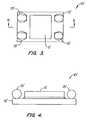
- FIG. 3is a plan view of another semiconductor device in accordance with the present invention.
- FIG. 4is a side sectional view of the semiconductor device illustrated FIG. 3 as seen along the line B-B;
- FIG. 5is a side sectional view of an alternative embodiment in accordance with the present invention.
- FIG. 1illustrates a MOSFET semiconductor device 10 that includes a die 11 , a substrate 12 and solder balls 13 .
- the substrateincludes a gate region 14 .
- the substratepreferably comprises a base layer 20 and a top, metal layer 21 .
- the base layer and the top metal layerare separated by an insulting layer 22 , preferably an insulating epoxy that joins the two layers.
- the base materialpreferably comprises a metallized pattern while the top metal layer preferably comprises another metallized pattern.
- the metal layermay also serve as a heat spreader.
- the dieis preferably coupled to the substrate with high temperature solder paste, but may also be coupled with any other suitable conductive interconnect known in the art.
- the solder ballsare placed adjacent the die on opposite sides of the die, with at least one solder ball being placed on the gate region of the substrate.
- the semiconductor deviceis placed on a printed circuit board and the surface of the die is coupled directly to the PCB with solder paste or suitable electrically conductive interconnect, and thus serves as the drain connection.
- the surface of the die coupled to the substratecomprises the gate region and the source region of the die.
- the solder ball in the gate region of the substrateserves to couple the gate region of the die to the PCB while the remaining solder balls couple the source region of the die through the substrate to the PCB. Accordingly, the gate region of the substrate is electrically isolated from the remaining portion of the substrate.
- a method of making or packaging such a semiconductor deviceincludes placing the solder paste on one of the substrate or the die and flip chip attaching the die to the substrate. Solder balls are then placed on the substrate adjacent the die. Preferably, this combination is then tested. The semiconductor device is then trimmed and the semiconductor device is retested.
- solder ballsare placed at a height such that when the semiconductor device is coupled to a PCB, the solder balls are substantially coplanar with the drain surface of the die, thus allowing the semiconductor device to be flush on the PCB.
- solder ballsare not placed on the semiconductor device, but rather are placed on the PCB and the semiconductor device is then coupled thereto.
- the substratecomprises a metallized ceramic.
- materials for the substrateinclude insulated metal substrate.
- the exposed surface of the dieserves as the drain connection to the PCB while the solder balls serve as the gate and source connections to the PCB.
- the device illustrated in FIGS. 3 and 4is manufactured in a manner similar to that described above with reference to the semiconductor device illustrated in FIGS. 1 and 2 .
- the present inventionprovides a semiconductor device that provides improved heat dissipation of the device since the die backside is soldered directly to the PCB and the source and gate of the MOSFET are soldered to a substrate, preferably via high temperature solder paste.
- the dieneed not be a bumped die but rather, needs a solderable top metal surface such as, for example, an electroless Nickel (or electrolytic Nickel) with a gold outer layer.
- the assembly processis simplified considerably since it does not involve form factor dedicated operations like wire bond, mold, deflash, trim and form, and plating. Also, the footprint is now changeable for the semiconductor arrangement since the solder balls are moveable during the design process.
- the present inventionalso allows for easily combining two or more dies 11 a, b in a high density packaging scheme (one or more die on each side of the substrate 12 ).
- a high density packaging schemeone or more die on each side of the substrate 12 .
- the substratecomprises two layers of metallized ceramic that are separated with an insulation layer or are otherwise electrically isolated.
- the placement of the solder ballsdetermines each die's source and gate connections. If it is desired to connect die 11 b 's drain to the PCB, known techniques such as wire bonding may be used.
Landscapes
- Engineering & Computer Science (AREA)
- Microelectronics & Electronic Packaging (AREA)
- Power Engineering (AREA)
- Physics & Mathematics (AREA)
- Condensed Matter Physics & Semiconductors (AREA)
- General Physics & Mathematics (AREA)
- Computer Hardware Design (AREA)
- Chemical & Material Sciences (AREA)
- Ceramic Engineering (AREA)
- Materials Engineering (AREA)
- Wire Bonding (AREA)
- Cooling Or The Like Of Semiconductors Or Solid State Devices (AREA)
Abstract
Description
- 1. Field of the Invention
- The present invention relates to a package for a semiconductor device, and more particularly, to a package for a semiconductor device that does not require a molded body.
- 2. Description of the Prior Art
- Semiconductor devices, especially MOSFET devices, generally desire very low package resistance (RDSon) with good thermal performance. It is also generally desirable to have simple, quick and efficient methods of packaging semiconductor devices. Thus, numerous packaging concepts and methods have been developed in the prior art.
- An example of one such packaging concept involves a ball grid array (BGA). Such a concept involves an array of source, gate and drain solder balls that are connected directly to the printed circuit board (PCB). This requires a bumped die and a leadframe is used to facilitate the drain contact. Another packaging concept is commonly referred to as Flip Chip in Leaded Molded Package (FLMP), which comprises a molded leaded surface mount package where a bumped die is connected to gate and source terminals of the frame. The drain, which is the back side of the die, is exposed from the mold compound or body and is connected to the PCB via solder reflow during a standard board mounting process. Other packaging concepts use copper straps and/or wire bond technology.
- These prior art concepts involve various components and may result in complicated manufacturing (packaging) processes.
- The present invention provides a semiconductor device that includes a substrate and a die coupled to the substrate. Multiple solder balls are also coupled to the substrate adjacent to the die. The solder balls are substantially coplanar with a surface of the die when the semiconductor device is coupled to a printed circuit board. Thus, when the semiconductor device is coupled to a PCB, the surface of the die not coupled to the substrate serves as a direct drain connection while the substrate and solder balls serve as the source and gate connections in the instance when the semiconductor device is a MOSFET device.
- In accordance with one aspect of the present invention, the substrate includes a base layer, a metal layer and an insulating layer between the base layer and the metal layer.
- In accordance with another aspect of the present invention, the base layer comprises a metallized pattern and the metal layer comprises another metallized pattern or serves as a heat spreader.
- In accordance with a further aspect of the present invention, the substrate is a metallized ceramic.
- In accordance with yet another aspect of the present invention, the substrate comprises two layers of metallized ceramic which can facilitate attachment of two dies (silicon) on opposite faces.
- The present invention also provides a method of packaging a semiconductor device that includes providing a substrate and a die. The solder, or any suitable electrically conductive interconnect in the case of MOSFET devices, is placed on at least one of the substrate and the die and the die is flipped onto the substrate. The solder balls are then placed on the substrate adjacent to the die.
- Other features and advantages of the present will be understood and upon reading and understanding the detailed description of the preferred exemplary embodiments found hereinbelow, in conjunction with reference to the drawings, in which like numerals represent like elements.
FIG. 1 is a plan view a semiconductor device in accordance with the present invention;FIG. 2 is a side sectional view of the semiconductor device illustrated inFIG. 1 as seen along the line A-A;FIG. 3 is a plan view of another semiconductor device in accordance with the present invention;FIG. 4 is a side sectional view of the semiconductor device illustratedFIG. 3 as seen along the line B-B; andFIG. 5 is a side sectional view of an alternative embodiment in accordance with the present invention.FIG. 1 illustrates aMOSFET semiconductor device 10 that includes a die11, asubstrate 12 andsolder balls 13. The substrate includes agate region 14.- As can be seen in
FIG. 2 , the substrate preferably comprises abase layer 20 and a top,metal layer 21. The base layer and the top metal layer are separated by aninsulting layer 22, preferably an insulating epoxy that joins the two layers. The base material preferably comprises a metallized pattern while the top metal layer preferably comprises another metallized pattern. The metal layer may also serve as a heat spreader. - The die is preferably coupled to the substrate with high temperature solder paste, but may also be coupled with any other suitable conductive interconnect known in the art. The solder balls are placed adjacent the die on opposite sides of the die, with at least one solder ball being placed on the gate region of the substrate.
- Thus, in use, the semiconductor device is placed on a printed circuit board and the surface of the die is coupled directly to the PCB with solder paste or suitable electrically conductive interconnect, and thus serves as the drain connection. The surface of the die coupled to the substrate comprises the gate region and the source region of the die. Thus, the solder ball in the gate region of the substrate serves to couple the gate region of the die to the PCB while the remaining solder balls couple the source region of the die through the substrate to the PCB. Accordingly, the gate region of the substrate is electrically isolated from the remaining portion of the substrate.
- A method of making or packaging such a semiconductor device includes placing the solder paste on one of the substrate or the die and flip chip attaching the die to the substrate. Solder balls are then placed on the substrate adjacent the die. Preferably, this combination is then tested. The semiconductor device is then trimmed and the semiconductor device is retested.
- The solder balls are placed at a height such that when the semiconductor device is coupled to a PCB, the solder balls are substantially coplanar with the drain surface of the die, thus allowing the semiconductor device to be flush on the PCB.
- In an alternative embodiment, the solder balls are not placed on the semiconductor device, but rather are placed on the PCB and the semiconductor device is then coupled thereto.
- With reference to
FIG. 3 , an alternative embodiment of the semiconductor device in accordance with the present invention is illustrated. In this embodiment, the substrate comprises a metallized ceramic. Examples of materials for the substrate include insulated metal substrate. - In such an embodiment, the exposed surface of the die serves as the drain connection to the PCB while the solder balls serve as the gate and source connections to the PCB.
- The device illustrated in
FIGS. 3 and 4 is manufactured in a manner similar to that described above with reference to the semiconductor device illustrated inFIGS. 1 and 2 . - Thus, the present invention provides a semiconductor device that provides improved heat dissipation of the device since the die backside is soldered directly to the PCB and the source and gate of the MOSFET are soldered to a substrate, preferably via high temperature solder paste. Thus, the die need not be a bumped die but rather, needs a solderable top metal surface such as, for example, an electroless Nickel (or electrolytic Nickel) with a gold outer layer. Furthermore, the assembly process is simplified considerably since it does not involve form factor dedicated operations like wire bond, mold, deflash, trim and form, and plating. Also, the footprint is now changeable for the semiconductor arrangement since the solder balls are moveable during the design process.
- As can be seen in
FIG. 5 , the present invention also allows for easily combining two or more dies11a, bin a high density packaging scheme (one or more die on each side of the substrate12). In doing so, an easy method of high density integration can be achieved without the use of conventional methods of surface mount package manufacture and that is form factor independent of steps such as mold, deflash, trim and form tooling. The substrate comprises two layers of metallized ceramic that are separated with an insulation layer or are otherwise electrically isolated. Thus, the placement of the solder balls determines each die's source and gate connections. If it is desired to connect die11b's drain to the PCB, known techniques such as wire bonding may be used. - Although the invention has been described with reference to specific exemplary embodiments, it will be appreciated that is intended to cover all modifications and equivalents within the scope of the appended claims.
Claims (16)
Priority Applications (1)
| Application Number | Priority Date | Filing Date | Title |
|---|---|---|---|
| US11/202,510US7393718B2 (en) | 2001-02-01 | 2005-08-11 | Unmolded package for a semiconductor device |
Applications Claiming Priority (4)
| Application Number | Priority Date | Filing Date | Title |
|---|---|---|---|
| US09/776,341US6469384B2 (en) | 2001-02-01 | 2001-02-01 | Unmolded package for a semiconductor device |
| US10/235,249US6740541B2 (en) | 2001-02-01 | 2002-09-04 | Unmolded package for a semiconductor device |
| US10/754,095US6953998B2 (en) | 2001-02-01 | 2003-12-29 | Unmolded package for a semiconductor device |
| US11/202,510US7393718B2 (en) | 2001-02-01 | 2005-08-11 | Unmolded package for a semiconductor device |
Related Parent Applications (1)
| Application Number | Title | Priority Date | Filing Date |
|---|---|---|---|
| US10/754,095ContinuationUS6953998B2 (en) | 2001-02-01 | 2003-12-29 | Unmolded package for a semiconductor device |
Publications (2)
| Publication Number | Publication Date |
|---|---|
| US20050280161A1true US20050280161A1 (en) | 2005-12-22 |
| US7393718B2 US7393718B2 (en) | 2008-07-01 |
Family
ID=25107113
Family Applications (4)
| Application Number | Title | Priority Date | Filing Date |
|---|---|---|---|
| US09/776,341Expired - Fee RelatedUS6469384B2 (en) | 2001-02-01 | 2001-02-01 | Unmolded package for a semiconductor device |
| US10/235,249Expired - LifetimeUS6740541B2 (en) | 2001-01-30 | 2002-09-04 | Unmolded package for a semiconductor device |
| US10/754,095Expired - LifetimeUS6953998B2 (en) | 2001-02-01 | 2003-12-29 | Unmolded package for a semiconductor device |
| US11/202,510Expired - Fee RelatedUS7393718B2 (en) | 2001-02-01 | 2005-08-11 | Unmolded package for a semiconductor device |
Family Applications Before (3)
| Application Number | Title | Priority Date | Filing Date |
|---|---|---|---|
| US09/776,341Expired - Fee RelatedUS6469384B2 (en) | 2001-02-01 | 2001-02-01 | Unmolded package for a semiconductor device |
| US10/235,249Expired - LifetimeUS6740541B2 (en) | 2001-01-30 | 2002-09-04 | Unmolded package for a semiconductor device |
| US10/754,095Expired - LifetimeUS6953998B2 (en) | 2001-02-01 | 2003-12-29 | Unmolded package for a semiconductor device |
Country Status (6)
| Country | Link |
|---|---|
| US (4) | US6469384B2 (en) |
| JP (2) | JP4729244B2 (en) |
| CN (2) | CN100576483C (en) |
| DE (1) | DE10295972B4 (en) |
| TW (1) | TW535243B (en) |
| WO (1) | WO2002061832A1 (en) |
Families Citing this family (84)
| Publication number | Priority date | Publication date | Assignee | Title |
|---|---|---|---|---|
| US6720642B1 (en)* | 1999-12-16 | 2004-04-13 | Fairchild Semiconductor Corporation | Flip chip in leaded molded package and method of manufacture thereof |
| US6989588B2 (en)* | 2000-04-13 | 2006-01-24 | Fairchild Semiconductor Corporation | Semiconductor device including molded wireless exposed drain packaging |
| US6870254B1 (en) | 2000-04-13 | 2005-03-22 | Fairchild Semiconductor Corporation | Flip clip attach and copper clip attach on MOSFET device |
| US6661082B1 (en)* | 2000-07-19 | 2003-12-09 | Fairchild Semiconductor Corporation | Flip chip substrate design |
| US6798044B2 (en)* | 2000-12-04 | 2004-09-28 | Fairchild Semiconductor Corporation | Flip chip in leaded molded package with two dies |
| US6753605B2 (en)* | 2000-12-04 | 2004-06-22 | Fairchild Semiconductor Corporation | Passivation scheme for bumped wafers |
| US6469384B2 (en)* | 2001-02-01 | 2002-10-22 | Fairchild Semiconductor Corporation | Unmolded package for a semiconductor device |
| US6891256B2 (en)* | 2001-10-22 | 2005-05-10 | Fairchild Semiconductor Corporation | Thin, thermally enhanced flip chip in a leaded molded package |
| AU2003218085A1 (en) | 2002-03-12 | 2003-09-29 | Fairchild Semiconductor Corporation | Wafer-level coated copper stud bumps |
| TWI287282B (en)* | 2002-03-14 | 2007-09-21 | Fairchild Kr Semiconductor Ltd | Semiconductor package having oxidation-free copper wire |
| US7122884B2 (en)* | 2002-04-16 | 2006-10-17 | Fairchild Semiconductor Corporation | Robust leaded molded packages and methods for forming the same |
| US6836023B2 (en)* | 2002-04-17 | 2004-12-28 | Fairchild Semiconductor Corporation | Structure of integrated trace of chip package |
| TW560023B (en)* | 2002-06-20 | 2003-11-01 | Advanced Semiconductor Eng | Semiconductor device and method for manufacturing a semiconductor package |
| US7061077B2 (en) | 2002-08-30 | 2006-06-13 | Fairchild Semiconductor Corporation | Substrate based unmolded package including lead frame structure and semiconductor die |
| US6777800B2 (en) | 2002-09-30 | 2004-08-17 | Fairchild Semiconductor Corporation | Semiconductor die package including drain clip |
| US6806580B2 (en)* | 2002-12-26 | 2004-10-19 | Fairchild Semiconductor Corporation | Multichip module including substrate with an array of interconnect structures |
| US7217594B2 (en)* | 2003-02-11 | 2007-05-15 | Fairchild Semiconductor Corporation | Alternative flip chip in leaded molded package design and method for manufacture |
| US7271497B2 (en)* | 2003-03-10 | 2007-09-18 | Fairchild Semiconductor Corporation | Dual metal stud bumping for flip chip applications |
| US6873043B2 (en)* | 2003-03-10 | 2005-03-29 | Delphi Technologies, Inc. | Electronic assembly having electrically-isolated heat-conductive structure |
| US6867481B2 (en)* | 2003-04-11 | 2005-03-15 | Fairchild Semiconductor Corporation | Lead frame structure with aperture or groove for flip chip in a leaded molded package |
| US7154186B2 (en)* | 2004-03-18 | 2006-12-26 | Fairchild Semiconductor Corporation | Multi-flip chip on lead frame on over molded IC package and method of assembly |
| US7196313B2 (en)* | 2004-04-02 | 2007-03-27 | Fairchild Semiconductor Corporation | Surface mount multi-channel optocoupler |
| US7501702B2 (en)* | 2004-06-24 | 2009-03-10 | Fairchild Semiconductor Corporation | Integrated transistor module and method of fabricating same |
| US7256479B2 (en)* | 2005-01-13 | 2007-08-14 | Fairchild Semiconductor Corporation | Method to manufacture a universal footprint for a package with exposed chip |
| WO2007005263A2 (en)* | 2005-06-30 | 2007-01-11 | Fairchild Semiconductor Corporation | Semiconductor die package and method for making the same |
| US7504733B2 (en) | 2005-08-17 | 2009-03-17 | Ciclon Semiconductor Device Corp. | Semiconductor die package |
| US7560808B2 (en)* | 2005-10-19 | 2009-07-14 | Texas Instruments Incorporated | Chip scale power LDMOS device |
| US7285849B2 (en)* | 2005-11-18 | 2007-10-23 | Fairchild Semiconductor Corporation | Semiconductor die package using leadframe and clip and method of manufacturing |
| US8018056B2 (en) | 2005-12-21 | 2011-09-13 | International Rectifier Corporation | Package for high power density devices |
| US20090057852A1 (en)* | 2007-08-27 | 2009-03-05 | Madrid Ruben P | Thermally enhanced thin semiconductor package |
| US7371616B2 (en)* | 2006-01-05 | 2008-05-13 | Fairchild Semiconductor Corporation | Clipless and wireless semiconductor die package and method for making the same |
| US7345499B2 (en)* | 2006-01-13 | 2008-03-18 | Dell Products L.P. | Method of Kelvin current sense in a semiconductor package |
| US20070164428A1 (en)* | 2006-01-18 | 2007-07-19 | Alan Elbanhawy | High power module with open frame package |
| US7868432B2 (en)* | 2006-02-13 | 2011-01-11 | Fairchild Semiconductor Corporation | Multi-chip module for battery power control |
| US7446375B2 (en)* | 2006-03-14 | 2008-11-04 | Ciclon Semiconductor Device Corp. | Quasi-vertical LDMOS device having closed cell layout |
| US7768075B2 (en)* | 2006-04-06 | 2010-08-03 | Fairchild Semiconductor Corporation | Semiconductor die packages using thin dies and metal substrates |
| US7618896B2 (en) | 2006-04-24 | 2009-11-17 | Fairchild Semiconductor Corporation | Semiconductor die package including multiple dies and a common node structure |
| US7656024B2 (en) | 2006-06-30 | 2010-02-02 | Fairchild Semiconductor Corporation | Chip module for complete power train |
| US20080036078A1 (en)* | 2006-08-14 | 2008-02-14 | Ciclon Semiconductor Device Corp. | Wirebond-less semiconductor package |
| US7564124B2 (en)* | 2006-08-29 | 2009-07-21 | Fairchild Semiconductor Corporation | Semiconductor die package including stacked dice and heat sink structures |
| US7768105B2 (en) | 2007-01-24 | 2010-08-03 | Fairchild Semiconductor Corporation | Pre-molded clip structure |
| US8106501B2 (en)* | 2008-12-12 | 2012-01-31 | Fairchild Semiconductor Corporation | Semiconductor die package including low stress configuration |
| US7821116B2 (en)* | 2007-02-05 | 2010-10-26 | Fairchild Semiconductor Corporation | Semiconductor die package including leadframe with die attach pad with folded edge |
| KR101391925B1 (en)* | 2007-02-28 | 2014-05-07 | 페어차일드코리아반도체 주식회사 | Semiconductor package and semiconductor package mold for fabricating the same |
| KR101489325B1 (en) | 2007-03-12 | 2015-02-06 | 페어차일드코리아반도체 주식회사 | Flip-chip type stacked power module and method of manufacturing the power module |
| US7659531B2 (en)* | 2007-04-13 | 2010-02-09 | Fairchild Semiconductor Corporation | Optical coupler package |
| US7683463B2 (en)* | 2007-04-19 | 2010-03-23 | Fairchild Semiconductor Corporation | Etched leadframe structure including recesses |
| US7902657B2 (en)* | 2007-08-28 | 2011-03-08 | Fairchild Semiconductor Corporation | Self locking and aligning clip structure for semiconductor die package |
| US7737548B2 (en) | 2007-08-29 | 2010-06-15 | Fairchild Semiconductor Corporation | Semiconductor die package including heat sinks |
| US20090057855A1 (en)* | 2007-08-30 | 2009-03-05 | Maria Clemens Quinones | Semiconductor die package including stand off structures |
| US20090140266A1 (en)* | 2007-11-30 | 2009-06-04 | Yong Liu | Package including oriented devices |
| US7589338B2 (en)* | 2007-11-30 | 2009-09-15 | Fairchild Semiconductor Corporation | Semiconductor die packages suitable for optoelectronic applications having clip attach structures for angled mounting of dice |
| KR20090062612A (en)* | 2007-12-13 | 2009-06-17 | 페어차일드코리아반도체 주식회사 | Multi-chip package |
| US7781872B2 (en)* | 2007-12-19 | 2010-08-24 | Fairchild Semiconductor Corporation | Package with multiple dies |
| US8426960B2 (en)* | 2007-12-21 | 2013-04-23 | Alpha & Omega Semiconductor, Inc. | Wafer level chip scale packaging |
| US8106406B2 (en)* | 2008-01-09 | 2012-01-31 | Fairchild Semiconductor Corporation | Die package including substrate with molded device |
| US7791084B2 (en) | 2008-01-09 | 2010-09-07 | Fairchild Semiconductor Corporation | Package with overlapping devices |
| US7626249B2 (en)* | 2008-01-10 | 2009-12-01 | Fairchild Semiconductor Corporation | Flex clip connector for semiconductor device |
| US7955893B2 (en)* | 2008-01-31 | 2011-06-07 | Alpha & Omega Semiconductor, Ltd | Wafer level chip scale package and process of manufacture |
| US20090194857A1 (en)* | 2008-02-01 | 2009-08-06 | Yong Liu | Thin Compact Semiconductor Die Packages Suitable for Smart-Power Modules, Methods of Making the Same, and Systems Using the Same |
| US20090194856A1 (en)* | 2008-02-06 | 2009-08-06 | Gomez Jocel P | Molded package assembly |
| KR101524545B1 (en)* | 2008-02-28 | 2015-06-01 | 페어차일드코리아반도체 주식회사 | Power device package and the method of fabricating the same |
| US7768108B2 (en) | 2008-03-12 | 2010-08-03 | Fairchild Semiconductor Corporation | Semiconductor die package including embedded flip chip |
| US8018054B2 (en)* | 2008-03-12 | 2011-09-13 | Fairchild Semiconductor Corporation | Semiconductor die package including multiple semiconductor dice |
| KR101519062B1 (en)* | 2008-03-31 | 2015-05-11 | 페어차일드코리아반도체 주식회사 | Semiconductor Device Package |
| US20090256245A1 (en)* | 2008-04-14 | 2009-10-15 | Yong Liu | Stacked Micro-Module Packages, Systems Using the Same, and Methods of Making the Same |
| US20090278241A1 (en)* | 2008-05-08 | 2009-11-12 | Yong Liu | Semiconductor die package including die stacked on premolded substrate including die |
| US20090315163A1 (en)* | 2008-06-20 | 2009-12-24 | Terry Johnson | Semiconductor Die Packages with Stacked Flexible Modules Having Passive Components, Systems Using the Same, and Methods of Making the Same |
| US7745244B2 (en) | 2008-06-23 | 2010-06-29 | Fairchild Semiconductor Corporation | Pin substrate and package |
| US8373257B2 (en)* | 2008-09-25 | 2013-02-12 | Alpha & Omega Semiconductor Incorporated | Top exposed clip with window array |
| US8193618B2 (en) | 2008-12-12 | 2012-06-05 | Fairchild Semiconductor Corporation | Semiconductor die package with clip interconnection |
| US7851856B2 (en)* | 2008-12-29 | 2010-12-14 | Alpha & Omega Semiconductor, Ltd | True CSP power MOSFET based on bottom-source LDMOS |
| US8049312B2 (en)* | 2009-01-12 | 2011-11-01 | Texas Instruments Incorporated | Semiconductor device package and method of assembly thereof |
| US7973393B2 (en) | 2009-02-04 | 2011-07-05 | Fairchild Semiconductor Corporation | Stacked micro optocouplers and methods of making the same |
| US8222718B2 (en)* | 2009-02-05 | 2012-07-17 | Fairchild Semiconductor Corporation | Semiconductor die package and method for making the same |
| US20100289129A1 (en)* | 2009-05-14 | 2010-11-18 | Satya Chinnusamy | Copper plate bonding for high performance semiconductor packaging |
| US8222078B2 (en)* | 2009-07-22 | 2012-07-17 | Alpha And Omega Semiconductor Incorporated | Chip scale surface mounted semiconductor device package and process of manufacture |
| US8362606B2 (en) | 2010-07-29 | 2013-01-29 | Alpha & Omega Semiconductor, Inc. | Wafer level chip scale package |
| US8421204B2 (en) | 2011-05-18 | 2013-04-16 | Fairchild Semiconductor Corporation | Embedded semiconductor power modules and packages |
| US8803297B2 (en)* | 2012-08-10 | 2014-08-12 | Infineon Technologies Ag | Semiconductor device including a stress relief layer and method of manufacturing |
| DE102014204722A1 (en)* | 2014-03-14 | 2015-09-17 | Robert Bosch Gmbh | Electronic module and method and apparatus for manufacturing an electronic module |
| CN105118817B (en)* | 2015-09-10 | 2017-09-19 | 江阴长电先进封装有限公司 | A kind of encapsulating structure and its method for packing of inexpensive silicon substrate module |
| US11862983B1 (en) | 2019-03-28 | 2024-01-02 | Roger W. Graham | Earth energy systems and devices |
| US11393743B2 (en) | 2019-12-18 | 2022-07-19 | Infineon Technologies Ag | Semiconductor assembly with conductive frame for I/O standoff and thermal dissipation |
Citations (26)
| Publication number | Priority date | Publication date | Assignee | Title |
|---|---|---|---|---|
| US4517051A (en)* | 1982-12-27 | 1985-05-14 | Ibm Corporation | Multi-layer flexible film module |
| US5159535A (en)* | 1987-03-11 | 1992-10-27 | International Business Machines Corporation | Method and apparatus for mounting a flexible film semiconductor chip carrier on a circuitized substrate |
| US5616958A (en)* | 1995-01-25 | 1997-04-01 | International Business Machines Corporation | Electronic package |
| US5637916A (en)* | 1996-02-02 | 1997-06-10 | National Semiconductor Corporation | Carrier based IC packaging arrangement |
| US5777386A (en)* | 1995-08-23 | 1998-07-07 | Shinko Electric Industries Co., Ltd. | Semiconductor device and mount structure thereof |
| US5789809A (en)* | 1995-08-22 | 1998-08-04 | National Semiconductor Corporation | Thermally enhanced micro-ball grid array package |
| US6023094A (en)* | 1998-01-14 | 2000-02-08 | National Semiconductor Corporation | Semiconductor wafer having a bottom surface protective coating |
| US6084308A (en)* | 1998-06-30 | 2000-07-04 | National Semiconductor Corporation | Chip-on-chip integrated circuit package and method for making the same |
| US6133634A (en)* | 1998-08-05 | 2000-10-17 | Fairchild Semiconductor Corporation | High performance flip chip package |
| US6137164A (en)* | 1998-03-16 | 2000-10-24 | Texas Instruments Incorporated | Thin stacked integrated circuit device |
| US6168973B1 (en)* | 1998-08-28 | 2001-01-02 | Medtronic, Inc. | Semiconductor stacked device for implantable medical apparatus and method for making same |
| US6225699B1 (en)* | 1998-06-26 | 2001-05-01 | International Business Machines Corporation | Chip-on-chip interconnections of varied characteristics |
| US6255143B1 (en)* | 1999-08-04 | 2001-07-03 | St. Assembly Test Services Pte Ltd. | Flip chip thermally enhanced ball grid array |
| US20020066959A1 (en)* | 2000-12-04 | 2002-06-06 | Rajeev Joshi | Passivation scheme for bumped wafers |
| US20020066950A1 (en)* | 2000-12-04 | 2002-06-06 | Fairchild Semiconductor Corporation | Flip chip in leaded molded package with two dies |
| US20020100962A1 (en)* | 2001-02-01 | 2002-08-01 | Rajeev Joshi | Unmolded package for a semiconductor device |
| US6462421B1 (en)* | 2000-04-10 | 2002-10-08 | Advanced Semicondcutor Engineering, Inc. | Multichip module |
| US20020192935A1 (en)* | 2001-06-15 | 2002-12-19 | Rajeev Joshi | Semiconductor die including conductive columns |
| US20030042403A1 (en)* | 2001-08-31 | 2003-03-06 | Fairchild Semiconductor Corporation | Surface mountable optocoupler package |
| US20030075786A1 (en)* | 2001-10-22 | 2003-04-24 | Fairchild Semiconductor Corporation | Thin, thermally enhanced flip chip in a leaded molded package |
| US6566749B1 (en)* | 2002-01-15 | 2003-05-20 | Fairchild Semiconductor Corporation | Semiconductor die package with improved thermal and electrical performance |
| US20030173684A1 (en)* | 2002-03-12 | 2003-09-18 | Rajeev Joshi | Wafer-level coated copper stud bumps |
| US20030197278A1 (en)* | 2002-04-17 | 2003-10-23 | Rajeev Joshi | Structure of integrated trace of chip package |
| US6661082B1 (en)* | 2000-07-19 | 2003-12-09 | Fairchild Semiconductor Corporation | Flip chip substrate design |
| US20040041242A1 (en)* | 2002-08-30 | 2004-03-04 | Fairchild Semiconductor Corporation | Substrate based unmolded package including lead frame structure and semiconductor die |
| US20040056364A1 (en)* | 1999-12-16 | 2004-03-25 | Fairchild Semiconductor Corporation | Flip chip in leaded molded package and method of manufacture thereof |
Family Cites Families (16)
| Publication number | Priority date | Publication date | Assignee | Title |
|---|---|---|---|---|
| JPS5974653A (en)* | 1982-10-22 | 1984-04-27 | Hitachi Ltd | Semiconductor device |
| JPS63104435A (en) | 1986-10-22 | 1988-05-09 | Hitachi Ltd | Semiconductor device |
| US5477082A (en)* | 1994-01-11 | 1995-12-19 | Exponential Technology, Inc. | Bi-planar multi-chip module |
| JP3348562B2 (en) | 1995-04-05 | 2002-11-20 | ソニー株式会社 | Semiconductor package mounting structure |
| JPH10284544A (en)* | 1997-04-10 | 1998-10-23 | Hitachi Ltd | Semiconductor device and manufacturing method thereof |
| US6049624A (en)* | 1998-02-20 | 2000-04-11 | Micron Technology, Inc. | Non-lot based method for assembling integrated circuit devices |
| JPH11238828A (en) | 1998-02-20 | 1999-08-31 | Toshiba Corp | Semiconductor device of BGA type package, method of manufacturing the same, and mounting device |
| EP0966038A3 (en)* | 1998-06-15 | 2001-02-28 | Ford Motor Company | Bonding of semiconductor power devices |
| US6226699B1 (en)* | 1998-06-25 | 2001-05-01 | Compaq Computer Corporation | Method and apparatus for clock selection and switching |
| JP2000077563A (en) | 1998-08-31 | 2000-03-14 | Sharp Corp | Semiconductor device and method of manufacturing the same |
| JP2000077591A (en)* | 1998-09-02 | 2000-03-14 | Sanken Electric Co Ltd | Semiconductor device and assembling method thereof |
| JP2000114413A (en)* | 1998-09-29 | 2000-04-21 | Sony Corp | Semiconductor device, its manufacture, and method for mounting parts |
| DK1156814T3 (en)* | 1999-03-03 | 2004-01-12 | Eurovita As | Pharmaceuticals, supplements and cosmetic preparations comprising a fatty acid and ginger |
| US6724083B2 (en)* | 2001-07-16 | 2004-04-20 | Ars Electronics Co., Ltd. | Method of producing semiconductor packages by cutting via holes into half when separating substrate |
| US6458695B1 (en)* | 2001-10-18 | 2002-10-01 | Chartered Semiconductor Manufacturing Ltd. | Methods to form dual metal gates by incorporating metals and their conductive oxides |
| US6620635B2 (en)* | 2002-02-20 | 2003-09-16 | International Business Machines Corporation | Damascene resistor and method for measuring the width of same |
- 2001
- 2001-02-01USUS09/776,341patent/US6469384B2/ennot_activeExpired - Fee Related
- 2002
- 2002-01-17JPJP2002561280Apatent/JP4729244B2/ennot_activeExpired - Fee Related
- 2002-01-17CNCN200710162352Apatent/CN100576483C/ennot_activeExpired - Fee Related
- 2002-01-17WOPCT/US2002/001686patent/WO2002061832A1/enactiveApplication Filing
- 2002-01-17DEDE10295972Tpatent/DE10295972B4/ennot_activeExpired - Fee Related
- 2002-01-17CNCNB028044363Apatent/CN100352047C/ennot_activeExpired - Fee Related
- 2002-01-25TWTW91101244Apatent/TW535243B/ennot_activeIP Right Cessation
- 2002-09-04USUS10/235,249patent/US6740541B2/ennot_activeExpired - Lifetime
- 2003
- 2003-12-29USUS10/754,095patent/US6953998B2/ennot_activeExpired - Lifetime
- 2005
- 2005-08-11USUS11/202,510patent/US7393718B2/ennot_activeExpired - Fee Related
- 2009
- 2009-02-18JPJP2009035263Apatent/JP2009124176A/enactivePending
Patent Citations (39)
| Publication number | Priority date | Publication date | Assignee | Title |
|---|---|---|---|---|
| US4517051A (en)* | 1982-12-27 | 1985-05-14 | Ibm Corporation | Multi-layer flexible film module |
| US5159535A (en)* | 1987-03-11 | 1992-10-27 | International Business Machines Corporation | Method and apparatus for mounting a flexible film semiconductor chip carrier on a circuitized substrate |
| US5616958A (en)* | 1995-01-25 | 1997-04-01 | International Business Machines Corporation | Electronic package |
| US5789809A (en)* | 1995-08-22 | 1998-08-04 | National Semiconductor Corporation | Thermally enhanced micro-ball grid array package |
| US5777386A (en)* | 1995-08-23 | 1998-07-07 | Shinko Electric Industries Co., Ltd. | Semiconductor device and mount structure thereof |
| US5637916A (en)* | 1996-02-02 | 1997-06-10 | National Semiconductor Corporation | Carrier based IC packaging arrangement |
| US5765280A (en)* | 1996-02-02 | 1998-06-16 | National Semiconductor Corporation | Method for making a carrier based IC packaging arrangement |
| US6175162B1 (en)* | 1998-01-14 | 2001-01-16 | National Semiconductor Corporation | Semiconductor wafer having a bottom surface protective coating |
| US6023094A (en)* | 1998-01-14 | 2000-02-08 | National Semiconductor Corporation | Semiconductor wafer having a bottom surface protective coating |
| US6137164A (en)* | 1998-03-16 | 2000-10-24 | Texas Instruments Incorporated | Thin stacked integrated circuit device |
| US6225699B1 (en)* | 1998-06-26 | 2001-05-01 | International Business Machines Corporation | Chip-on-chip interconnections of varied characteristics |
| US6084308A (en)* | 1998-06-30 | 2000-07-04 | National Semiconductor Corporation | Chip-on-chip integrated circuit package and method for making the same |
| US6133634A (en)* | 1998-08-05 | 2000-10-17 | Fairchild Semiconductor Corporation | High performance flip chip package |
| US6489678B1 (en)* | 1998-08-05 | 2002-12-03 | Fairchild Semiconductor Corporation | High performance multi-chip flip chip package |
| US6294403B1 (en)* | 1998-08-05 | 2001-09-25 | Rajeev Joshi | High performance flip chip package |
| US20030122247A1 (en)* | 1998-08-05 | 2003-07-03 | Fairchild Semiconductor Corporation | High performance multi-chip flip chip package |
| US6627991B1 (en)* | 1998-08-05 | 2003-09-30 | Fairchild Semiconductor Corporation | High performance multi-chip flip package |
| US20030107126A1 (en)* | 1998-08-05 | 2003-06-12 | Fairchild Semiconductor Corporation | High performance multi-chip flip chip package |
| US6696321B2 (en)* | 1998-08-05 | 2004-02-24 | Fairchild Semiconductor, Corporation | High performance multi-chip flip chip package |
| US6168973B1 (en)* | 1998-08-28 | 2001-01-02 | Medtronic, Inc. | Semiconductor stacked device for implantable medical apparatus and method for making same |
| US6255143B1 (en)* | 1999-08-04 | 2001-07-03 | St. Assembly Test Services Pte Ltd. | Flip chip thermally enhanced ball grid array |
| US6479903B2 (en)* | 1999-08-04 | 2002-11-12 | St Assembly Test Services Ltd. | Flip chip thermally enhanced ball grid array |
| US20040056364A1 (en)* | 1999-12-16 | 2004-03-25 | Fairchild Semiconductor Corporation | Flip chip in leaded molded package and method of manufacture thereof |
| US6462421B1 (en)* | 2000-04-10 | 2002-10-08 | Advanced Semicondcutor Engineering, Inc. | Multichip module |
| US6661082B1 (en)* | 2000-07-19 | 2003-12-09 | Fairchild Semiconductor Corporation | Flip chip substrate design |
| US20020066950A1 (en)* | 2000-12-04 | 2002-06-06 | Fairchild Semiconductor Corporation | Flip chip in leaded molded package with two dies |
| US20020066959A1 (en)* | 2000-12-04 | 2002-06-06 | Rajeev Joshi | Passivation scheme for bumped wafers |
| US20020100962A1 (en)* | 2001-02-01 | 2002-08-01 | Rajeev Joshi | Unmolded package for a semiconductor device |
| US20030011005A1 (en)* | 2001-02-01 | 2003-01-16 | Fairchild Semiconductor Corporation | Unmolded package for a semiconductor device |
| US6469384B2 (en)* | 2001-02-01 | 2002-10-22 | Fairchild Semiconductor Corporation | Unmolded package for a semiconductor device |
| US6683375B2 (en)* | 2001-06-15 | 2004-01-27 | Fairchild Semiconductor Corporation | Semiconductor die including conductive columns |
| US20020192935A1 (en)* | 2001-06-15 | 2002-12-19 | Rajeev Joshi | Semiconductor die including conductive columns |
| US20030042403A1 (en)* | 2001-08-31 | 2003-03-06 | Fairchild Semiconductor Corporation | Surface mountable optocoupler package |
| US6633030B2 (en)* | 2001-08-31 | 2003-10-14 | Fiarchild Semiconductor | Surface mountable optocoupler package |
| US20030075786A1 (en)* | 2001-10-22 | 2003-04-24 | Fairchild Semiconductor Corporation | Thin, thermally enhanced flip chip in a leaded molded package |
| US6566749B1 (en)* | 2002-01-15 | 2003-05-20 | Fairchild Semiconductor Corporation | Semiconductor die package with improved thermal and electrical performance |
| US20030173684A1 (en)* | 2002-03-12 | 2003-09-18 | Rajeev Joshi | Wafer-level coated copper stud bumps |
| US20030197278A1 (en)* | 2002-04-17 | 2003-10-23 | Rajeev Joshi | Structure of integrated trace of chip package |
| US20040041242A1 (en)* | 2002-08-30 | 2004-03-04 | Fairchild Semiconductor Corporation | Substrate based unmolded package including lead frame structure and semiconductor die |
Also Published As
| Publication number | Publication date |
|---|---|
| CN101154607A (en) | 2008-04-02 |
| TW535243B (en) | 2003-06-01 |
| CN100352047C (en) | 2007-11-28 |
| WO2002061832A1 (en) | 2002-08-08 |
| US7393718B2 (en) | 2008-07-01 |
| US20020100962A1 (en) | 2002-08-01 |
| JP2004521493A (en) | 2004-07-15 |
| US20040164386A1 (en) | 2004-08-26 |
| US20030011005A1 (en) | 2003-01-16 |
| US6953998B2 (en) | 2005-10-11 |
| DE10295972T5 (en) | 2004-04-15 |
| CN1489788A (en) | 2004-04-14 |
| JP2009124176A (en) | 2009-06-04 |
| JP4729244B2 (en) | 2011-07-20 |
| US6469384B2 (en) | 2002-10-22 |
| DE10295972B4 (en) | 2013-05-16 |
| CN100576483C (en) | 2009-12-30 |
| US6740541B2 (en) | 2004-05-25 |
Similar Documents
| Publication | Publication Date | Title |
|---|---|---|
| US7393718B2 (en) | Unmolded package for a semiconductor device | |
| TWI281238B (en) | Thermal enhanced package for block mold assembly | |
| US8513059B2 (en) | Pre-molded clip structure | |
| CN101213663B (en) | Semiconductor die package and manufacturing method thereof | |
| US6566164B1 (en) | Exposed copper strap in a semiconductor package | |
| US7618896B2 (en) | Semiconductor die package including multiple dies and a common node structure | |
| US6191487B1 (en) | Semiconductor and flip chip packages and method having a back-side connection | |
| US7821124B2 (en) | Thin, thermally enhanced flip chip in a leaded molded package | |
| US5583377A (en) | Pad array semiconductor device having a heat sink with die receiving cavity | |
| US6856007B2 (en) | High-frequency chip packages | |
| US20040157372A1 (en) | Alternative flip chip in leaded molded package design and method for manufacture | |
| US6731000B1 (en) | Folded-flex bondwire-less multichip power package | |
| US20100193922A1 (en) | Semiconductor chip package | |
| JP2009302564A (en) | Ic chip package with directly connected leads | |
| US12300583B2 (en) | Concealed gate terminal semiconductor packages and related methods | |
| US20150243641A1 (en) | Integrated circuit package | |
| US7808088B2 (en) | Semiconductor device with improved high current performance | |
| TWI283048B (en) | New package system for discrete devices | |
| JP2810130B2 (en) | Semiconductor package | |
| KR200179419Y1 (en) | Semiconductor package |
Legal Events
| Date | Code | Title | Description |
|---|---|---|---|
| STCF | Information on status: patent grant | Free format text:PATENTED CASE | |
| FPAY | Fee payment | Year of fee payment:4 | |
| FPAY | Fee payment | Year of fee payment:8 | |
| SULP | Surcharge for late payment | Year of fee payment:7 | |
| AS | Assignment | Owner name:DEUTSCHE BANK AG NEW YORK BRANCH, AS COLLATERAL AGENT, NEW YORK Free format text:PATENT SECURITY AGREEMENT;ASSIGNOR:FAIRCHILD SEMICONDUCTOR CORPORATION;REEL/FRAME:040075/0644 Effective date:20160916 Owner name:DEUTSCHE BANK AG NEW YORK BRANCH, AS COLLATERAL AG Free format text:PATENT SECURITY AGREEMENT;ASSIGNOR:FAIRCHILD SEMICONDUCTOR CORPORATION;REEL/FRAME:040075/0644 Effective date:20160916 | |
| FEPP | Fee payment procedure | Free format text:MAINTENANCE FEE REMINDER MAILED (ORIGINAL EVENT CODE: REM.); ENTITY STATUS OF PATENT OWNER: LARGE ENTITY | |
| LAPS | Lapse for failure to pay maintenance fees | Free format text:PATENT EXPIRED FOR FAILURE TO PAY MAINTENANCE FEES (ORIGINAL EVENT CODE: EXP.); ENTITY STATUS OF PATENT OWNER: LARGE ENTITY | |
| STCH | Information on status: patent discontinuation | Free format text:PATENT EXPIRED DUE TO NONPAYMENT OF MAINTENANCE FEES UNDER 37 CFR 1.362 | |
| FP | Lapsed due to failure to pay maintenance fee | Effective date:20200701 | |
| AS | Assignment | Owner name:SEMICONDUCTOR COMPONENTS INDUSTRIES, LLC, ARIZONA Free format text:ASSIGNMENT OF ASSIGNORS INTEREST;ASSIGNOR:FAIRCHILD SEMICONDUCTOR CORPORATION;REEL/FRAME:057694/0374 Effective date:20210722 | |
| AS | Assignment | Owner name:FAIRCHILD SEMICONDUCTOR CORPORATION, ARIZONA Free format text:RELEASE BY SECURED PARTY;ASSIGNOR:DEUTSCHE BANK AG NEW YORK BRANCH;REEL/FRAME:057969/0206 Effective date:20211027 | |
| AS | Assignment | Owner name:DEUTSCHE BANK AG NEW YORK BRANCH, AS COLLATERAL AGENT, NEW YORK Free format text:SECURITY INTEREST;ASSIGNOR:SEMICONDUCTOR COMPONENTS INDUSTRIES, LLC;REEL/FRAME:058871/0799 Effective date:20211028 | |
| AS | Assignment | Owner name:FAIRCHILD SEMICONDUCTOR CORPORATION, ARIZONA Free format text:RELEASE OF SECURITY INTEREST IN PATENTS RECORDED AT REEL 040075, FRAME 0644;ASSIGNOR:DEUTSCHE BANK AG NEW YORK BRANCH, AS COLLATERAL AGENT;REEL/FRAME:064070/0536 Effective date:20230622 Owner name:SEMICONDUCTOR COMPONENTS INDUSTRIES, LLC, ARIZONA Free format text:RELEASE OF SECURITY INTEREST IN PATENTS RECORDED AT REEL 040075, FRAME 0644;ASSIGNOR:DEUTSCHE BANK AG NEW YORK BRANCH, AS COLLATERAL AGENT;REEL/FRAME:064070/0536 Effective date:20230622 | |
| AS | Assignment | Owner name:FAIRCHILD SEMICONDUCTOR CORPORATION, ARIZONA Free format text:RELEASE OF SECURITY INTEREST IN PATENTS RECORDED AT REEL 058871, FRAME 0799;ASSIGNOR:DEUTSCHE BANK AG NEW YORK BRANCH, AS COLLATERAL AGENT;REEL/FRAME:065653/0001 Effective date:20230622 Owner name:SEMICONDUCTOR COMPONENTS INDUSTRIES, LLC, ARIZONA Free format text:RELEASE OF SECURITY INTEREST IN PATENTS RECORDED AT REEL 058871, FRAME 0799;ASSIGNOR:DEUTSCHE BANK AG NEW YORK BRANCH, AS COLLATERAL AGENT;REEL/FRAME:065653/0001 Effective date:20230622 |