US20050280135A1 - Stacking system and method - Google Patents
Stacking system and methodDownload PDFInfo
- Publication number
- US20050280135A1 US20050280135A1US11/197,267US19726705AUS2005280135A1US 20050280135 A1US20050280135 A1US 20050280135A1US 19726705 AUS19726705 AUS 19726705AUS 2005280135 A1US2005280135 A1US 2005280135A1
- Authority
- US
- United States
- Prior art keywords
- flex
- contacts
- csp
- module
- csps
- Prior art date
- Legal status (The legal status is an assumption and is not a legal conclusion. Google has not performed a legal analysis and makes no representation as to the accuracy of the status listed.)
- Granted
Links
Images


Classifications
- H—ELECTRICITY
- H01—ELECTRIC ELEMENTS
- H01L—SEMICONDUCTOR DEVICES NOT COVERED BY CLASS H10
- H01L23/00—Details of semiconductor or other solid state devices
- H01L23/28—Encapsulations, e.g. encapsulating layers, coatings, e.g. for protection
- H01L23/31—Encapsulations, e.g. encapsulating layers, coatings, e.g. for protection characterised by the arrangement or shape
- H01L23/3107—Encapsulations, e.g. encapsulating layers, coatings, e.g. for protection characterised by the arrangement or shape the device being completely enclosed
- H01L23/3114—Encapsulations, e.g. encapsulating layers, coatings, e.g. for protection characterised by the arrangement or shape the device being completely enclosed the device being a chip scale package, e.g. CSP
- H—ELECTRICITY
- H01—ELECTRIC ELEMENTS
- H01L—SEMICONDUCTOR DEVICES NOT COVERED BY CLASS H10
- H01L23/00—Details of semiconductor or other solid state devices
- H01L23/48—Arrangements for conducting electric current to or from the solid state body in operation, e.g. leads, terminal arrangements ; Selection of materials therefor
- H01L23/488—Arrangements for conducting electric current to or from the solid state body in operation, e.g. leads, terminal arrangements ; Selection of materials therefor consisting of soldered or bonded constructions
- H01L23/498—Leads, i.e. metallisations or lead-frames on insulating substrates, e.g. chip carriers
- H01L23/49811—Additional leads joined to the metallisation on the insulating substrate, e.g. pins, bumps, wires, flat leads
- H01L23/49816—Spherical bumps on the substrate for external connection, e.g. ball grid arrays [BGA]
- H—ELECTRICITY
- H01—ELECTRIC ELEMENTS
- H01L—SEMICONDUCTOR DEVICES NOT COVERED BY CLASS H10
- H01L23/00—Details of semiconductor or other solid state devices
- H01L23/48—Arrangements for conducting electric current to or from the solid state body in operation, e.g. leads, terminal arrangements ; Selection of materials therefor
- H01L23/488—Arrangements for conducting electric current to or from the solid state body in operation, e.g. leads, terminal arrangements ; Selection of materials therefor consisting of soldered or bonded constructions
- H01L23/498—Leads, i.e. metallisations or lead-frames on insulating substrates, e.g. chip carriers
- H01L23/49827—Via connections through the substrates, e.g. pins going through the substrate, coaxial cables
- H—ELECTRICITY
- H01—ELECTRIC ELEMENTS
- H01L—SEMICONDUCTOR DEVICES NOT COVERED BY CLASS H10
- H01L23/00—Details of semiconductor or other solid state devices
- H01L23/48—Arrangements for conducting electric current to or from the solid state body in operation, e.g. leads, terminal arrangements ; Selection of materials therefor
- H01L23/488—Arrangements for conducting electric current to or from the solid state body in operation, e.g. leads, terminal arrangements ; Selection of materials therefor consisting of soldered or bonded constructions
- H01L23/498—Leads, i.e. metallisations or lead-frames on insulating substrates, e.g. chip carriers
- H01L23/49838—Geometry or layout
- H—ELECTRICITY
- H01—ELECTRIC ELEMENTS
- H01L—SEMICONDUCTOR DEVICES NOT COVERED BY CLASS H10
- H01L23/00—Details of semiconductor or other solid state devices
- H01L23/48—Arrangements for conducting electric current to or from the solid state body in operation, e.g. leads, terminal arrangements ; Selection of materials therefor
- H01L23/488—Arrangements for conducting electric current to or from the solid state body in operation, e.g. leads, terminal arrangements ; Selection of materials therefor consisting of soldered or bonded constructions
- H01L23/498—Leads, i.e. metallisations or lead-frames on insulating substrates, e.g. chip carriers
- H01L23/4985—Flexible insulating substrates
- H—ELECTRICITY
- H01—ELECTRIC ELEMENTS
- H01L—SEMICONDUCTOR DEVICES NOT COVERED BY CLASS H10
- H01L23/00—Details of semiconductor or other solid state devices
- H01L23/48—Arrangements for conducting electric current to or from the solid state body in operation, e.g. leads, terminal arrangements ; Selection of materials therefor
- H01L23/50—Arrangements for conducting electric current to or from the solid state body in operation, e.g. leads, terminal arrangements ; Selection of materials therefor for integrated circuit devices, e.g. power bus, number of leads
- H—ELECTRICITY
- H01—ELECTRIC ELEMENTS
- H01L—SEMICONDUCTOR DEVICES NOT COVERED BY CLASS H10
- H01L23/00—Details of semiconductor or other solid state devices
- H01L23/52—Arrangements for conducting electric current within the device in operation from one component to another, i.e. interconnections, e.g. wires, lead frames
- H01L23/538—Arrangements for conducting electric current within the device in operation from one component to another, i.e. interconnections, e.g. wires, lead frames the interconnection structure between a plurality of semiconductor chips being formed on, or in, insulating substrates
- H01L23/5387—Flexible insulating substrates
- H—ELECTRICITY
- H01—ELECTRIC ELEMENTS
- H01L—SEMICONDUCTOR DEVICES NOT COVERED BY CLASS H10
- H01L25/00—Assemblies consisting of a plurality of semiconductor or other solid state devices
- H01L25/03—Assemblies consisting of a plurality of semiconductor or other solid state devices all the devices being of a type provided for in a single subclass of subclasses H10B, H10D, H10F, H10H, H10K or H10N, e.g. assemblies of rectifier diodes
- H01L25/04—Assemblies consisting of a plurality of semiconductor or other solid state devices all the devices being of a type provided for in a single subclass of subclasses H10B, H10D, H10F, H10H, H10K or H10N, e.g. assemblies of rectifier diodes the devices not having separate containers
- H01L25/065—Assemblies consisting of a plurality of semiconductor or other solid state devices all the devices being of a type provided for in a single subclass of subclasses H10B, H10D, H10F, H10H, H10K or H10N, e.g. assemblies of rectifier diodes the devices not having separate containers the devices being of a type provided for in group H10D89/00
- H01L25/0657—Stacked arrangements of devices
- H—ELECTRICITY
- H01—ELECTRIC ELEMENTS
- H01L—SEMICONDUCTOR DEVICES NOT COVERED BY CLASS H10
- H01L25/00—Assemblies consisting of a plurality of semiconductor or other solid state devices
- H01L25/03—Assemblies consisting of a plurality of semiconductor or other solid state devices all the devices being of a type provided for in a single subclass of subclasses H10B, H10D, H10F, H10H, H10K or H10N, e.g. assemblies of rectifier diodes
- H01L25/10—Assemblies consisting of a plurality of semiconductor or other solid state devices all the devices being of a type provided for in a single subclass of subclasses H10B, H10D, H10F, H10H, H10K or H10N, e.g. assemblies of rectifier diodes the devices having separate containers
- H01L25/105—Assemblies consisting of a plurality of semiconductor or other solid state devices all the devices being of a type provided for in a single subclass of subclasses H10B, H10D, H10F, H10H, H10K or H10N, e.g. assemblies of rectifier diodes the devices having separate containers the devices being integrated devices of class H10
- H—ELECTRICITY
- H05—ELECTRIC TECHNIQUES NOT OTHERWISE PROVIDED FOR
- H05K—PRINTED CIRCUITS; CASINGS OR CONSTRUCTIONAL DETAILS OF ELECTRIC APPARATUS; MANUFACTURE OF ASSEMBLAGES OF ELECTRICAL COMPONENTS
- H05K1/00—Printed circuits
- H05K1/02—Details
- H05K1/14—Structural association of two or more printed circuits
- H05K1/141—One or more single auxiliary printed circuits mounted on a main printed circuit, e.g. modules, adapters
- H—ELECTRICITY
- H05—ELECTRIC TECHNIQUES NOT OTHERWISE PROVIDED FOR
- H05K—PRINTED CIRCUITS; CASINGS OR CONSTRUCTIONAL DETAILS OF ELECTRIC APPARATUS; MANUFACTURE OF ASSEMBLAGES OF ELECTRICAL COMPONENTS
- H05K1/00—Printed circuits
- H05K1/02—Details
- H05K1/14—Structural association of two or more printed circuits
- H05K1/147—Structural association of two or more printed circuits at least one of the printed circuits being bent or folded, e.g. by using a flexible printed circuit
- H—ELECTRICITY
- H01—ELECTRIC ELEMENTS
- H01L—SEMICONDUCTOR DEVICES NOT COVERED BY CLASS H10
- H01L2224/00—Indexing scheme for arrangements for connecting or disconnecting semiconductor or solid-state bodies and methods related thereto as covered by H01L24/00
- H01L2224/01—Means for bonding being attached to, or being formed on, the surface to be connected, e.g. chip-to-package, die-attach, "first-level" interconnects; Manufacturing methods related thereto
- H01L2224/10—Bump connectors; Manufacturing methods related thereto
- H01L2224/15—Structure, shape, material or disposition of the bump connectors after the connecting process
- H01L2224/16—Structure, shape, material or disposition of the bump connectors after the connecting process of an individual bump connector
- H01L2224/161—Disposition
- H01L2224/16151—Disposition the bump connector connecting between a semiconductor or solid-state body and an item not being a semiconductor or solid-state body, e.g. chip-to-substrate, chip-to-passive
- H01L2224/16221—Disposition the bump connector connecting between a semiconductor or solid-state body and an item not being a semiconductor or solid-state body, e.g. chip-to-substrate, chip-to-passive the body and the item being stacked
- H01L2224/16225—Disposition the bump connector connecting between a semiconductor or solid-state body and an item not being a semiconductor or solid-state body, e.g. chip-to-substrate, chip-to-passive the body and the item being stacked the item being non-metallic, e.g. insulating substrate with or without metallisation
- H01L2224/16237—Disposition the bump connector connecting between a semiconductor or solid-state body and an item not being a semiconductor or solid-state body, e.g. chip-to-substrate, chip-to-passive the body and the item being stacked the item being non-metallic, e.g. insulating substrate with or without metallisation the bump connector connecting to a bonding area disposed in a recess of the surface of the item
- H—ELECTRICITY
- H01—ELECTRIC ELEMENTS
- H01L—SEMICONDUCTOR DEVICES NOT COVERED BY CLASS H10
- H01L2224/00—Indexing scheme for arrangements for connecting or disconnecting semiconductor or solid-state bodies and methods related thereto as covered by H01L24/00
- H01L2224/73—Means for bonding being of different types provided for in two or more of groups H01L2224/10, H01L2224/18, H01L2224/26, H01L2224/34, H01L2224/42, H01L2224/50, H01L2224/63, H01L2224/71
- H01L2224/732—Location after the connecting process
- H01L2224/73251—Location after the connecting process on different surfaces
- H01L2224/73253—Bump and layer connectors
- H—ELECTRICITY
- H01—ELECTRIC ELEMENTS
- H01L—SEMICONDUCTOR DEVICES NOT COVERED BY CLASS H10
- H01L2225/00—Details relating to assemblies covered by the group H01L25/00 but not provided for in its subgroups
- H01L2225/03—All the devices being of a type provided for in the same main group of the same subclass of class H10, e.g. assemblies of rectifier diodes
- H01L2225/04—All the devices being of a type provided for in the same main group of the same subclass of class H10, e.g. assemblies of rectifier diodes the devices not having separate containers
- H01L2225/065—All the devices being of a type provided for in the same main group of the same subclass of class H10
- H01L2225/06503—Stacked arrangements of devices
- H01L2225/06517—Bump or bump-like direct electrical connections from device to substrate
- H—ELECTRICITY
- H01—ELECTRIC ELEMENTS
- H01L—SEMICONDUCTOR DEVICES NOT COVERED BY CLASS H10
- H01L2225/00—Details relating to assemblies covered by the group H01L25/00 but not provided for in its subgroups
- H01L2225/03—All the devices being of a type provided for in the same main group of the same subclass of class H10, e.g. assemblies of rectifier diodes
- H01L2225/04—All the devices being of a type provided for in the same main group of the same subclass of class H10, e.g. assemblies of rectifier diodes the devices not having separate containers
- H01L2225/065—All the devices being of a type provided for in the same main group of the same subclass of class H10
- H01L2225/06503—Stacked arrangements of devices
- H01L2225/06541—Conductive via connections through the device, e.g. vertical interconnects, through silicon via [TSV]
- H—ELECTRICITY
- H01—ELECTRIC ELEMENTS
- H01L—SEMICONDUCTOR DEVICES NOT COVERED BY CLASS H10
- H01L2225/00—Details relating to assemblies covered by the group H01L25/00 but not provided for in its subgroups
- H01L2225/03—All the devices being of a type provided for in the same main group of the same subclass of class H10, e.g. assemblies of rectifier diodes
- H01L2225/04—All the devices being of a type provided for in the same main group of the same subclass of class H10, e.g. assemblies of rectifier diodes the devices not having separate containers
- H01L2225/065—All the devices being of a type provided for in the same main group of the same subclass of class H10
- H01L2225/06503—Stacked arrangements of devices
- H01L2225/06579—TAB carriers; beam leads
- H—ELECTRICITY
- H01—ELECTRIC ELEMENTS
- H01L—SEMICONDUCTOR DEVICES NOT COVERED BY CLASS H10
- H01L2225/00—Details relating to assemblies covered by the group H01L25/00 but not provided for in its subgroups
- H01L2225/03—All the devices being of a type provided for in the same main group of the same subclass of class H10, e.g. assemblies of rectifier diodes
- H01L2225/04—All the devices being of a type provided for in the same main group of the same subclass of class H10, e.g. assemblies of rectifier diodes the devices not having separate containers
- H01L2225/065—All the devices being of a type provided for in the same main group of the same subclass of class H10
- H01L2225/06503—Stacked arrangements of devices
- H01L2225/06582—Housing for the assembly, e.g. chip scale package [CSP]
- H01L2225/06586—Housing with external bump or bump-like connectors
- H—ELECTRICITY
- H01—ELECTRIC ELEMENTS
- H01L—SEMICONDUCTOR DEVICES NOT COVERED BY CLASS H10
- H01L2225/00—Details relating to assemblies covered by the group H01L25/00 but not provided for in its subgroups
- H01L2225/03—All the devices being of a type provided for in the same main group of the same subclass of class H10, e.g. assemblies of rectifier diodes
- H01L2225/10—All the devices being of a type provided for in the same main group of the same subclass of class H10, e.g. assemblies of rectifier diodes the devices having separate containers
- H01L2225/1005—All the devices being of a type provided for in the same main group of the same subclass of class H10, e.g. assemblies of rectifier diodes the devices having separate containers the devices being integrated devices of class H10
- H01L2225/1011—All the devices being of a type provided for in the same main group of the same subclass of class H10, e.g. assemblies of rectifier diodes the devices having separate containers the devices being integrated devices of class H10 the containers being in a stacked arrangement
- H01L2225/1047—Details of electrical connections between containers
- H01L2225/107—Indirect electrical connections, e.g. via an interposer, a flexible substrate, using TAB
- H—ELECTRICITY
- H01—ELECTRIC ELEMENTS
- H01L—SEMICONDUCTOR DEVICES NOT COVERED BY CLASS H10
- H01L2924/00—Indexing scheme for arrangements or methods for connecting or disconnecting semiconductor or solid-state bodies as covered by H01L24/00
- H01L2924/0001—Technical content checked by a classifier
- H01L2924/00014—Technical content checked by a classifier the subject-matter covered by the group, the symbol of which is combined with the symbol of this group, being disclosed without further technical details
- H—ELECTRICITY
- H01—ELECTRIC ELEMENTS
- H01L—SEMICONDUCTOR DEVICES NOT COVERED BY CLASS H10
- H01L2924/00—Indexing scheme for arrangements or methods for connecting or disconnecting semiconductor or solid-state bodies as covered by H01L24/00
- H01L2924/01—Chemical elements
- H01L2924/01055—Cesium [Cs]
- H—ELECTRICITY
- H01—ELECTRIC ELEMENTS
- H01L—SEMICONDUCTOR DEVICES NOT COVERED BY CLASS H10
- H01L2924/00—Indexing scheme for arrangements or methods for connecting or disconnecting semiconductor or solid-state bodies as covered by H01L24/00
- H01L2924/15—Details of package parts other than the semiconductor or other solid state devices to be connected
- H01L2924/151—Die mounting substrate
- H01L2924/1517—Multilayer substrate
- H01L2924/15172—Fan-out arrangement of the internal vias
- H01L2924/15173—Fan-out arrangement of the internal vias in a single layer of the multilayer substrate
- H—ELECTRICITY
- H01—ELECTRIC ELEMENTS
- H01L—SEMICONDUCTOR DEVICES NOT COVERED BY CLASS H10
- H01L2924/00—Indexing scheme for arrangements or methods for connecting or disconnecting semiconductor or solid-state bodies as covered by H01L24/00
- H01L2924/15—Details of package parts other than the semiconductor or other solid state devices to be connected
- H01L2924/151—Die mounting substrate
- H01L2924/153—Connection portion
- H01L2924/1531—Connection portion the connection portion being formed only on the surface of the substrate opposite to the die mounting surface
- H01L2924/15311—Connection portion the connection portion being formed only on the surface of the substrate opposite to the die mounting surface being a ball array, e.g. BGA
- H—ELECTRICITY
- H01—ELECTRIC ELEMENTS
- H01L—SEMICONDUCTOR DEVICES NOT COVERED BY CLASS H10
- H01L2924/00—Indexing scheme for arrangements or methods for connecting or disconnecting semiconductor or solid-state bodies as covered by H01L24/00
- H01L2924/19—Details of hybrid assemblies other than the semiconductor or other solid state devices to be connected
- H01L2924/1901—Structure
- H01L2924/1904—Component type
- H01L2924/19041—Component type being a capacitor
- H—ELECTRICITY
- H01—ELECTRIC ELEMENTS
- H01L—SEMICONDUCTOR DEVICES NOT COVERED BY CLASS H10
- H01L2924/00—Indexing scheme for arrangements or methods for connecting or disconnecting semiconductor or solid-state bodies as covered by H01L24/00
- H01L2924/30—Technical effects
- H01L2924/301—Electrical effects
- H01L2924/3011—Impedance
- H—ELECTRICITY
- H05—ELECTRIC TECHNIQUES NOT OTHERWISE PROVIDED FOR
- H05K—PRINTED CIRCUITS; CASINGS OR CONSTRUCTIONAL DETAILS OF ELECTRIC APPARATUS; MANUFACTURE OF ASSEMBLAGES OF ELECTRICAL COMPONENTS
- H05K1/00—Printed circuits
- H05K1/18—Printed circuits structurally associated with non-printed electric components
- H05K1/189—Printed circuits structurally associated with non-printed electric components characterised by the use of a flexible or folded printed circuit
- H—ELECTRICITY
- H05—ELECTRIC TECHNIQUES NOT OTHERWISE PROVIDED FOR
- H05K—PRINTED CIRCUITS; CASINGS OR CONSTRUCTIONAL DETAILS OF ELECTRIC APPARATUS; MANUFACTURE OF ASSEMBLAGES OF ELECTRICAL COMPONENTS
- H05K2201/00—Indexing scheme relating to printed circuits covered by H05K1/00
- H05K2201/05—Flexible printed circuits [FPCs]
- H05K2201/056—Folded around rigid support or component
- H—ELECTRICITY
- H05—ELECTRIC TECHNIQUES NOT OTHERWISE PROVIDED FOR
- H05K—PRINTED CIRCUITS; CASINGS OR CONSTRUCTIONAL DETAILS OF ELECTRIC APPARATUS; MANUFACTURE OF ASSEMBLAGES OF ELECTRICAL COMPONENTS
- H05K2201/00—Indexing scheme relating to printed circuits covered by H05K1/00
- H05K2201/10—Details of components or other objects attached to or integrated in a printed circuit board
- H05K2201/10613—Details of electrical connections of non-printed components, e.g. special leads
- H05K2201/10621—Components characterised by their electrical contacts
- H05K2201/10689—Leaded Integrated Circuit [IC] package, e.g. dual-in-line [DIL]
- H—ELECTRICITY
- H05—ELECTRIC TECHNIQUES NOT OTHERWISE PROVIDED FOR
- H05K—PRINTED CIRCUITS; CASINGS OR CONSTRUCTIONAL DETAILS OF ELECTRIC APPARATUS; MANUFACTURE OF ASSEMBLAGES OF ELECTRICAL COMPONENTS
- H05K2201/00—Indexing scheme relating to printed circuits covered by H05K1/00
- H05K2201/10—Details of components or other objects attached to or integrated in a printed circuit board
- H05K2201/10613—Details of electrical connections of non-printed components, e.g. special leads
- H05K2201/10621—Components characterised by their electrical contacts
- H05K2201/10734—Ball grid array [BGA]; Bump grid array
- H—ELECTRICITY
- H05—ELECTRIC TECHNIQUES NOT OTHERWISE PROVIDED FOR
- H05K—PRINTED CIRCUITS; CASINGS OR CONSTRUCTIONAL DETAILS OF ELECTRIC APPARATUS; MANUFACTURE OF ASSEMBLAGES OF ELECTRICAL COMPONENTS
- H05K3/00—Apparatus or processes for manufacturing printed circuits
- H05K3/36—Assembling printed circuits with other printed circuits
- H05K3/361—Assembling flexible printed circuits with other printed circuits
- H05K3/363—Assembling flexible printed circuits with other printed circuits by soldering
Definitions
- the present inventionrelates to aggregating integrated circuits and, in particular, to stacking integrated circuits in chip-scale packages.
- a variety of techniquesare used to stack packaged integrated circuits. Some methods require special packages, while other techniques stack conventional packages. In some stacks, the leads of the packaged integrated circuits are used to create a stack, while in other systems, added structures such as rails provide all or part of the interconnection between packages. In still other techniques, flexible conductors with certain characteristics are used to selectively interconnect packaged integrated circuits.
- the predominant package configuration employed during the past decadehas encapsulated an integrated circuit (IC) in a plastic surround typically having a rectangular configuration.
- ICintegrated circuit
- the enveloped integrated circuitis connected to the application environment through leads emergent from the edge periphery of the plastic encapsulation.
- Such “leaded packages”have been the constituent elements most commonly employed by techniques for stacking packaged integrated circuits.
- Leaded packagesplay an important role in electronics, but efforts to miniaturize electronic components and assemblies have driven development of technologies that preserve circuit board surface area. Because leaded packages have leads emergent from peripheral sides of the package, leaded packages occupy more than a minimal amount of circuit board surface area. Consequently, alternatives to leaded packages have recently gained market share.
- CSPchip scale packaging
- CSPCSP leads or contacts do not typically extend beyond the outline perimeter of the package.
- the absence of “leads” on package sidesrenders most stacking techniques devised for leaded packages inapplicable for CSP stacking.
- CSPhas enabled reductions in size and weight parameters for many applications.
- micro ball grid array ( ⁇ BGA) for flash and SRAM and wirebond on tape or rigid laminate CSPs for SRAM or EEPROMhave been employed in a variety of applications.
- CSPis a broad category including a variety of packages from near chip scale to die-sized packages such as the die sized ball grid array (DSBGA) recently described in proposed JEDEC standard 95-1 for DSBGA.
- DSBGAdie sized ball grid array
- the assignee of the present inventionhas developed previous systems for aggregating ⁇ BGA packages in space saving topologies.
- the assignee of the present inventionhas systems for stacking BGA packages on a DIMM in a RAMBUS environment.
- Thermal performanceis a characteristic of importance in CSP stacks. To increase dissipation of heat generated by constituent CSPs, the thermal gradient between the lower CSP and upper CSP in a CSP stack or module should be minimized. Prior art solutions to CSP stacking do not, however, address thermal gradient minimization in disclosed constructions.
- the present inventionstacks chip scale-packaged integrated circuits (CSPs) into modules that conserve PWB or other board surface area.
- CSPschip scale-packaged integrated circuits
- two CSPsare stacked, with one CSP disposed above the other.
- the two CSPsare connected with flex circuitry.
- a form standardis disposed between the flex circuitry and a CSP in the stack.
- the form standardcan take many configurations and may be used where flex circuits are used to connect CSPs to one another in stacked modules having two or more constituent ICs. For example, in stacked modules that include four CSPs, three form standards are employed in preferred embodiments, although fewer may be used.
- the form standardprovides a physical form that allows many of the varying package sizes found in the broad family of CSP packages to be used to advantage while employing a standard connective flex circuitry design.
- the form standardwill be devised of heat transference (thermally conductive) material.
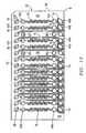
- FIG. 1is an elevation view of module 10 devised in accordance with a preferred embodiment of the present invention.
- FIG. 2is an elevation view of module 10 devised in accordance with a preferred embodiment of the present invention.
- FIG. 3depicts, in enlarged view, the area marked “A” in FIG. 2 .
- FIG. 4is an enlarged detail of an exemplar connection in a preferred embodiment of the present invention.
- FIG. 5is an enlarged depiction of an exemplar area around a lower flex contact in a preferred embodiment of the present invention.
- FIG. 6depicts a first outer surface layer of a flex circuit employed in a preferred embodiment of the present invention.
- FIG. 7depicts a first outer surface layer of a flex circuit employed in a preferred embodiment of the present invention.
- FIG. 8depicts a first conductive layer of a flex circuit employed in a preferred embodiment of the present invention.
- FIG. 9illustrates a first conductive layer of a flex circuit employed in a preferred embodiment of the present invention.
- FIG. 10depicts an intermediate layer of a flex circuit employed in a preferred embodiment of the present invention.
- FIG. 11depicts an intermediate layer of a right side flex circuit employed in a preferred embodiment of the present invention.
- FIG. 12depicts a second conductive layer of a flex circuit of a preferred embodiment of the present invention.
- FIG. 13depicts a second conductive layer of a flex circuit of a preferred embodiment of the present invention.
- FIG. 14depicts a second outer layer of a flex circuit employed in a preferred embodiment of the present invention.
- FIG. 15reflects a second outer layer of a flex circuit employed in a preferred embodiment of the present invention.
- FIG. 16depicts an alternative preferred embodiment of the present invention.
- FIG. 17illustrates a JEDEC pinout for DDR-II FBGA packages.
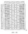
- FIG. 18illustrates the pinout of a module 10 in an alternative preferred embodiment of the invention.
- FIG. 19illustrates the pinout of a module 10 in an alternative embodiment of the invention.
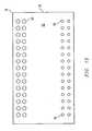
- FIG. 20depicts the pinout of an exemplar CSP employed in a preferred embodiment of the invention.
- FIG. 21depicts a second conductive layer of a flex circuit employed in an alternative preferred embodiment of the present invention.
- FIG. 22depicts a second conductive layer of a flex circuit employed in an alternative preferred embodiment of the present invention.
- FIG. 23depicts a module devised in accordance with a preferred embodiment of the present invention.
- FIG. 24is an enlarged depiction of a portion of the embodiment depicted in FIG. 23 .
- FIG. 25depicts a portion of a module devised in accordance with an alternative embodiment of the present invention.
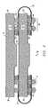
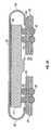
- FIG. 1is an elevation view of module 10 devised in accordance with a preferred embodiment of the present invention.
- Module 10is comprised of upper CSP 12 and lower CSP 14 .
- Each of CSPs 12 and 14have an upper surface 16 and a lower surface 18 and opposite lateral sides 20 and 22 .
- CSPschip scale packaged integrated circuits
- FIGS. 1 and 2are depicted with CSPs of a particular profile known to those in the art, but it should be understood that the figures are exemplary only.
- CSPssuch as, for example, ball-grid-array (“BGA”), micro-ball-grid array (“ ⁇ BGA”), and fine-pitch ball grid array (“FBGA”) packages have an array of connective contacts embodied, for example, as leads, bumps, solder balls, or balls that extend from lower surface 18 of a plastic casing in any of several patterns and pitches. An external portion of the connective contacts is often finished with a ball of solder. Shown in FIG. 1 are CSP contacts 24 along lower surfaces 18 of CSPs 12 and 14 . CSP contacts 24 provide connection to the integrated circuit within the respective packages. Collectively, CSP contacts 24 comprise CSP array 26 shown as to lower CSP 14 in the depicted particular package configuration as CSP arrays 26 , and 262 which collectively comprise CSP array 26 .
- BGAball-grid-array
- ⁇ BGAmicro-ball-grid array
- FBGAfine-pitch ball grid array
- flex circuits(“flex”, “flex circuits” or “flexible circuit structures”) 30 and 32 are shown partially wrapped about lower CSP 14 with flex 30 partially wrapped over lateral side 20 of lower CSP 14 and flex 32 partially wrapped about lateral side 22 of lower CSP 14 .
- Lateral sides 20 and 22may be in the character of sides or may, if the CSP is especially thin, be in the character of an edge. Any flexible or conformable substrate with a multiple internal layer connectivity capability may be used as a flex circuit in the invention.
- the entire flex circuitmay be flexible or, as those of skill in the art will recognize, a PCB structure made flexible in certain areas to allow conformability around lower CSP 14 and rigid in other areas for planarity along CSP surfaces may be employed as an alternative flex circuit in the present invention.
- structures known as rigid-flexmay be employed.
- Portions of flex circuits 30 and 32are fixed to upper surface 16 of lower CSP 14 by adhesive 34 which is shown as a tape adhesive, but may be a liquid adhesive or may be placed in discrete locations across the package.
- adhesive 34is thermally conductive. Adhesives that include a flux are used to advantage in assembly of module 10 .
- Layer 34may also be a thermally conductive medium to encourage heat flow between the CSPs of module 10 .
- Flex circuits 30 and 32are multi-layer flexible circuit structures that have at least two conductive layers.
- the conductive layersare metal such as alloy 110 .
- the use of plural conductive layersprovides advantages as will be seen and the creation of a distributed capacitance across module 10 intended to reduce noise or bounce effects that can, particularly at higher frequencies, degrade signal integrity, as those of skill in the art will recognize.
- Module 10 of FIG. 1has module contacts 36 collectively identified as module array 38 .
- FIG. 2shows a module 10 devised in accordance with a preferred embodiment of the invention.
- FIG. 2illustrates use of a conformal media 40 provided in a preferred embodiment to assist in creating conformality of structural areas of module 10 .
- Planarity of the moduleis improved by conformal media 40 .
- conformal media 40is thermally conductive.
- thermal spreaders or a thermal mediummay be placed as shown by reference 41 .
- Identified in FIG. 2are upper flex contacts 42 and lower flex contacts 44 that are at one of the conductive layers of flex circuits 30 and 32 .
- Upper flex contacts 42 and lower flex contacts 44are conductive material and, preferably, are solid metal.
- Lower flex contacts 44are collectively lower flex contact array 46 .
- Upper flex contacts 42are collectively upper flex contact array 48 . Only some of upper flex contacts 42 and lower flex contacts 44 are identified in FIG. 2 to preserve clarity of the view. It should be understood that each of flex circuits 30 and 32 have both upper flex contacts 42 and lower flex contacts 44 . Lower flex contacts 44 are employed with lower CSP 14 and upper flex contacts 42 are employed with upper CSP 12 .
- FIG. 2has an area marked “A” that is subsequently shown in enlarged depiction in FIG. 3 .
- FIG. 3depicts in enlarged view, the area marked “A” in FIG. 2 .
- FIG. 3illustrates the connection between example CSP contact 24 and module contact 36 through lower flex contact 44 to illustrate the solid metal path from lower CSP 14 to module contact 36 and, therefore, to an application PWB to which module is connectable. As those of skill in the art will understand, heat transference from module 10 is thereby encouraged.
- CSP contact 24 and module contact 36together offset module 10 from an application platform such as a PWB.
- the combined heights of CSP contact 24 and module contact 36provide a moment arm longer than the height of a single CSP contact 24 alone. This provides a longer moment arm through which temperature-gradient-over-time stresses (such as typified by temp cycle), can be distributed.
- Flex 30is shown in FIG. 3 to be comprised of multiple layers. Flex 30 has a first outer surface 50 and a second outer surface 52 . Flex circuit 30 has at least two conductive layers interior to first and second outer surfaces 50 and 52 . There may be more than two conductive layers in flex 30 and flex 32 . In the depicted preferred embodiment, first conductive layer 54 and second conductive layer 58 are interior to first and second outer surfaces 50 and 52 . Intermediate layer 56 lies between first conductive layer 54 and second conductive layer 58 . There may be more than one intermediate layer, but one intermediate layer of polyimide is preferred.
- lower flex contact 44is preferably comprised from metal at the level of second conductive layer 58 interior to second outer surface 52 .
- Lower flex contact 44is solid metal in a preferred embodiment and is comprised of metal alloy such as alloy 110 . This results in a solid metal pathway from lower CSP 14 to an application board thereby providing a significant thermal pathway for dissipation of heat generated in module 10 .
- FIG. 4is an enlarged detail of an exemplar connection between example CSP contact 24 and example module contact 36 through lower flex contact 44 to illustrate the solid metal path from lower CSP 14 to module contact 36 and, therefore, to an application PWB to which module 10 is connectable.
- lower flex contact 44is at second conductive layer 58 that is interior to first and second outer surface layers 50 and 52 respectively, of flex circuit 30 .
- FIG. 5is an enlarged depiction of an exemplar area around a lower flex contact 44 in a preferred embodiment.
- Windows 60 and 62are opened in first and second outer surface layers 50 and 52 respectively, to provide access to particular lower flex contacts 44 residing at the level of second conductive layer 58 in the flex.
- the upper flex contacts 42are contacted by CSP contacts 24 of upper CSP 12 .
- Lower flex contacts 44 and upper flex contacts 42are particular areas of conductive material (preferably metal such as alloy 110 ) at the level of second conductive layer 58 in the flex.
- Upper flex contacts 42 and lower flex contacts 44are demarked in second conductive layer 58 and, as will be shown in subsequent Figs., may be connected to or isolated from the conductive plane of second conductive layer 58 .
- Demarking a lower flex contact 44 from second conductive layer 58is represented in FIG. 5 by demarcation gap 63 shown at second conductive layer 58 .
- demarcation gapsdo not extend completely around the flex contact as shown, for example, by lower flex contacts 44 C in later FIG. 12 .
- CSP contacts 24 of lower CSP 14pass through a window 60 opened through first outer surface layer 50 , first conductive layer 54 , and intermediate layer 56 , to contact an appropriate lower flex contact 44 .
- Window 62is opened through second outer surface layer 52 through which module contacts 36 pass to contact the appropriate lower flex contact 44 .
- Respective ones of CSP contacts 24 of upper CSP 12 and lower CSP 14are connected at the second conductive layer 58 level in flex circuits 30 and 32 to interconnect appropriate signal and voltage contacts of the two CSPs.
- Respective CSP contacts 24 of upper CSP 12 and lower CSP 14 that convey ground (VSS) signalsare connected at the first conductive layer 54 level in flex circuits 30 and 32 by vias that pass through intermediate layer 56 to connect the levels as will subsequently be described in further detail.
- CSPs 12 and 14are connected. Consequently, when flex circuits 30 and 32 are in place about lower CSP 14 , respective CSP contacts 24 of each of upper and lower CSPs 12 and 14 are in contact with upper and lower flex contacts 42 and 44 , respectively. Selected ones of upper flex contacts 42 and lower flex contacts 44 are connected. Consequently, by being in contact with lower flex contacts 44 , module contacts 36 are in contact with both upper and lower CSPs 12 and 14 .
- module contacts 36pass through windows 62 opened in second outer layer 52 to contact lower CSP contacts 44 .
- module 10will exhibit a module contact array 38 that has a greater number of contacts than do the constituent CSPs of module 10 .
- some of module contacts 36may contact lower flex contacts 44 that do not contact one of the CSP contacts 24 of lower CSP 14 but are connected to CSP contacts 24 of upper CSP 12 . This allows module 10 to express a wider datapath than that expressed by the constituent CSPs 12 or 14 .
- a module contact 36may also be in contact with a lower flex contact 44 to provide a location through which different levels of CSPs in the module may be enabled when no unused CSP contacts are available or convenient for that purpose.
- first conductive layer 54is employed as a ground plane, while second conductive layer 58 provides the functions of being a signal conduction layer and a voltage conduction layer.
- first and second conductive layersmay be reversed with attendant changes in windowing and use of commensurate interconnections.
- first and second conductive layers 54 and 58there is at least one intermediate layer 56 that, in a preferred embodiment, is a polyimide. Placement of such an intermediate layer between ground-conductive first conductive layer 54 and signal/voltage conductive second conductive layer 58 provides, in the combination, a distributed capacitance that assists in mitigation of ground bounce phenomena to improve high frequency performance of module 10 .
- FIG. 6depicts first outer surface layer 50 of flex 30 (i.e., left side of FIG. 1 ). The view is from above the flex looking down into flex 30 from the perspective of first conductive layer 54 . Throughout the Figs., the location reference “B” is to orient views of layers of flex 30 to those of flex 32 as well as across layers. Windows 60 are opened through first outer surface layer 50 , first conductive layer 54 , and intermediate layer 56 . CSP contacts 24 of lower CSP 14 pass through windows 60 of first outer surface layer 50 , first conductive layer 54 , and intermediate layer 56 to reach the level of second conductive layer 58 of flex 30 .
- selected CSP contacts 24 of lower CSP 14make contact with selected lower flex contacts 44 .
- Lower flex contacts 44provide several types of connection in a preferred embodiment as will be explained with reference to later FIG. 12 .
- a portion of flex 30will be wrapped about lateral side 20 of lower CSP 14 to place edge 62 above upper surface 16 of lower CSP 14 .
- FIG. 7depicts first outer surface layer 50 of flex 32 (i.e., right side of FIG. 1 ).
- the viewis from above the flex looking down into flex 32 from the perspective of first conductive layer 54 .
- the location reference “B”relatively orients the views of FIGS. 6 and 7 .
- the views of FIGS. 6 and 7may be understood together with the reference marks “B” of each view being placed nearer each other than to any other corner of the other view of the pair of views of the same layer.
- windows 60are opened through first outer surface layer 50 , first conductive layer 54 and intermediate layer 56 .
- CSP contacts 24 of lower CSP 14pass through windows 60 of first outer surface layer 50 , first conductive layer 54 , and intermediate layer 56 to reach the level of second conductive layer 58 of flex 30 .
- selected CSP contacts 24 of lower CSP 14make contact with lower flex contacts 44 .
- Lower flex contacts 44provide several types of connection in a preferred embodiment as will be explained with reference to later FIG. 12 .
- FIG. 8depicts first conductive layer 54 of flex 30 .
- Windows 60continue the opened orifice in flex 30 through which CSP contacts 24 of lower CSP 14 pass to reach second conductive layer 58 and, therefore, selected lower flex contacts 44 at the level of second conductive layer 58 .
- first conductive layer 54becomes, on the part of flex 30 disposed above upper surface 16 of lower CSP 14 , the lower-most conductive layer of flex 30 from the perspective of upper CSP 12 .
- those CSP contacts 24 of upper CSP 12 that provide ground (VSS) connectionsare connected to the first conductive layer 54 .
- First conductive layer 54lies beneath, however, second conductive layer 58 in that part of flex 30 that is wrapped above lower CSP 14 . Consequently, some means must be provided for connection of the upper flex contact 42 to which ground-conveying CSP contacts 24 of upper CSP 12 are connected and first conductive layer 54 .
- those upper flex contacts 42 that are in contact with ground-conveying CSP contacts 24 of upper CSP 12have vias that route through intermediate layer 56 to reach first conductive layer 54 .
- the sites where those vias meet first conductive layer 54are identified in FIG. 8 as vias 66 .
- These viasmay be “on-pad” or coincident with the flex contact 42 to which they are connected.
- vias 66 in FIG. 8are one via.
- vias in the figuresare shown larger in diameter than in manufactured embodiments.
- connection between conductive layers provided by viasmay be provided any of several well-known techniques such as plated holes or solid lines or wires and need not literally be vias.
- Off-pad vias 74are disposed on first conductive layer 54 at locations near, but not coincident with selected ones of windows 60 . Unlike vias 66 that connect selected ones of upper flex contacts 42 to first conductive layer 54 , off-pad vias 74 connect selected ones of lower flex contacts 44 to first conductive layer 54 . In the vicinity of upper flex contacts 42 , second conductive layer 58 is between the CSP connected to module 10 by the upper flex contacts 42 (i.e., upper CSP 12 ) and first conductive layer 54 .
- first conductive layer 54is between the CSP connected to module 10 by the lower flex contacts 44 (i.e., lower CSP 14 ) and second conductive layer 58 . Consequently, vias between ground-conveying lower flex contacts 44 and first conductive layer 54 are offset from the selected lower flex contacts 44 by off-pad vias 74 shown in offset locations.
- FIG. 9illustrates first conductive layer 54 of flex 32 .
- the location reference marks “B”are employed to relatively orient FIGS. 8 and 9 .
- Windows 60 , vias 66 and off-pad vias 74are identified in FIG. 9 .
- Enable via 70is connected off-pad to a selected lower flex contact 44 that corresponds, in this preferred embodiment, to an unused CSP contact 24 of lower CSP 14 (i.e., a N/C).
- a module contact 36 at that siteconveys an enable signal (C/S) for upper CSP 12 through the selected lower flex contact 44 (which is at the level of second conductive layer 58 ) to off-pad enable via 70 that conveys the enable signal to first conductive layer 54 and thereby to enable trace 72 .
- Enable trace 72further conveys the enable signal to enable via 68 which extends through intermediate layer 56 to selected upper flex contact 42 at the level of second conductive layer 58 where contact is made with the C/S pin of upper CSP 12 .
- upper and lower CSPs 12 and 14may be independently enabled.
- FIG. 10depicts intermediate layer 56 of flex 30 .
- Windows 60are shown opened in intermediate surface 56 .
- CSP contacts 24 of lower CSP 14pass through windows 60 in intermediate layer 58 to reach lower flex contacts 44 at the level of second conductive layer 58 .
- windows 60narrow in diameter from their manifestation in first outer layer 50 .
- Vias 66 , off-pad vias 74 , and enable vias 68 and 70pass through intermediate layer 56 connecting selected conductive areas at the level of first and second conductive layers 54 and 58 , respectively.
- FIG. 11depicts intermediate layer 56 of flex 32 showing windows 60 , vias 66 , off-pad vias 74 , and enable vias 68 and 70 passing through intermediate layer 56 .
- FIG. 12depicts second conductive layer 58 of flex 30 of a preferred embodiment of the present invention. Depicted are various types of upper flex contacts 42 , various types of lower flex contacts 44 , signal traces 76 , and VDD plane 78 as well as previously described vias 66 and off-pad vias 74 . Throughout FIGS. 12 and 13 , only exemplars of particular features are identified to preserve clarity of the view. Flex contacts 44 A are connected to corresponding selected upper flex contacts 42 A with signal traces 76 . To enhance the clarity of the view, only exemplar individual flex contacts 44 A and 42 A are literally identified in FIG. 12 .
- signal traces 76exhibit path routes determined to provide substantially equal signal lengths between corresponding flex contacts 42 A and 44 A. As shown, traces 76 are separated from the larger surface area of second conductive layer 58 that is identified as VDD plane 78 . VDD plane 78 may be in one or more delineated sections but, preferably is one section. Lower flex contacts 44 C provide connection to VDD plane 78 . In a preferred embodiment, upper flex contacts 42 C and lower flex contacts 44 C connect upper CSP 12 and lower CSP 14 , respectively, to VDD plane 78 . Lower flex contacts 44 that are connected to first conductive layer 54 by off-pad vias 74 are identified as lower flex contacts 44 B. To enhance the clarity of the view, only exemplar individual lower flex contacts 44 B are literally identified in FIG. 12 . Upper flex contacts 42 that are connected to first conductive layer 54 by vias 66 are identified as upper flex contacts 42 B.
- FIG. 13depicts second conductive layer 58 of right side flex 32 of a preferred embodiment of the present invention. Depicted are various types of upper flex contacts 42 , various types of lower flex contacts 44 , signal traces 76 , and VDD plane 78 as well as previously described vias 66 , off-pad vias 74 , and enable vias 70 and 68 .
- FIG. 13illustrates upper flex contacts 42 A connected by traces 76 to lower flex contacts 44 A.
- VDD plane 78provides a voltage plane at the level of second conductive layer 58 .
- Lower flex contacts 44 C and upper flex contacts 42 Cconnect lower CSP 14 and upper CSP 12 , respectively, to VDD plane 78 .
- Lower flex contact 44 Dis shown with enable via 70 described earlier.
- Corresponding upper flex contact 42 Dis connected to lower flex contact 44 D through enable vias 70 and 68 that are connected to each other through earlier described enable trace 72 at the first conductive layer 54 level of flex 32 .
- FIG. 14depicts second outer layer 52 of flex 30 .
- Windows 62are identified. Those of skill will recognize that module contacts 36 pass through windows 62 to contact appropriate lower flex contacts 44 .
- flex 30is partially wrapped about lateral side 20 of lower CSP 14 , a portion of second outer layer 52 becomes the upper-most layer of flex 30 from the perspective of upper CSP 12 .
- CSP contacts 24 of upper CSP 12pass through windows 64 to reach second conductive layer 58 and make contact with appropriate ones of upper flex contacts 42 located at that level.
- FIG. 15reflects second outer layer 52 of flex 32 and exhibits windows 64 and 62 .
- Module contacts 36pass through windows 62 to contact appropriate lower flex contacts 44 .
- CSP contacts 24 of upper CSP 12pass through windows 64 to reach second conductive layer 58 and make contact with appropriate ones of upper flex contacts 42 located at that level.
- FIG. 16depicts an alternative preferred embodiment of the present invention showing module 10 .
- module contacts 36 Esupply a part of the datapath of module 10 and may provide a facility for differential enablement of the constituent CSPs.
- a module contact 36 E not employed in wide datapath provisionmay provide a contact point to supply an enable signal to differentially enable upper CSP 12 or lower CSP 14 .
- a wide datapath module 10the data paths of the constituent upper CSP 12 and lower CSP 14 are combined to provide a module 10 that expresses a module datapath that is twice the width of the datapaths of the constituent CSPs in a two-high module 10 .
- the preferred method of combinationis concatenation, but other combinations may be employed to combine the datapaths of CSPs 12 and 14 on the array of module contacts 36 and 36 E.
- FIGS. 17, 18 , and 19are provided to illustrate using added module contacts 36 E in alternative embodiments of the present invention to provide wider datapaths for module 10 than are present in constituent CSPs 12 and 14 .
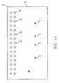
- FIG. 17illustrates a JEDEC pinout for DDR-II FBGA packages.
- FIG. 18illustrates the pinout provided by module contacts 36 and 36 E of a module 10 expressing an 8-bit wide datapath.
- Module 10is devised in accordance with the present invention and is, in the exemplar embodiment, comprised of an upper CSP 12 and lower CSP 14 that are DDR-II-compliant in timing, but each of which are only 4 bits wide in datapath. As will be recognized, the module 10 mapped in FIG.
- FIG. 18expresses an 8-bit wide datapath.
- FIG. 18depicts DQ pins differentiated in source between upper CSP 12 (“top”) and lower CSP 14 (“bot”) to aggregate to 8-bits.
- FIG. 19illustrates the pinout provided by module contacts 36 and 36 E of module 10 expressing a 16-bit wide datapath.
- Module 10is devised in accordance with the present invention and is, in this exemplar embodiment, comprised of an upper CSP 12 and lower CSP 14 that are DDR-II-compliant in timing, but each of which are only 8-bits wide in datapath.
- the wide datapath embodimentmay be employed with any of a variety of CSPs available in the field and such CSPs need not be DDR compliant.
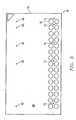
- FIG. 20illustrates a typical pinout of a memory circuit provided as a CSP and useable in the present invention. Individual array positions are identified by the JEDEC convention of numbered columns and alphabetic rows. The central area (e.g., A 3 -A 6 ; B 3 -B 6 ; etc.) is unpopulated. CSP contacts 24 are present at the locations that are identified by alpha-numeric identifiers such as, for example, A 3 , shown as an example CSP contact 24 .
- FIG. 21depicts second metal layer 58 of flex 30 in an alternative embodiment of the invention in which module 10 expresses a datapath wider than that expressed by either of the the constituent CSPs 12 and 14 .
- Lower flex contacts 44 Eare not contacted by CSP contacts 24 of lower CSP 14 , but are contacted by module contacts 36 E to provide, with selected module contacts 36 , a datapath for module 10 that is 2n-bits in width where the datapaths of CSPs 12 and 14 have a width of n-bits.
- lower flex contacts 44 Eare connected to upper flex contacts 42 E.
- windows 62pass through second outer layer 52 .
- module contacts 36 and 36 Epass through windows 62 in second outer layer 52 of flex circuit 30 , to contact appropriate lower flex contacts 44 .
- FIG. 22illustrates second metal layer 58 of flex 32 in an alternative embodiment of the invention in which module 10 expresses a datapath wider than that expressed by either of the the constituent CSPs 12 and 14 .
- Lower flex contacts 44 Eare not contacted by CSP contacts 24 of lower CSP 14 , but are contacted by module contacts 36 E to provide, with selected module contacts 36 , a datapath for module 10 that is 2n-bits in width where the datapaths of CSPs 12 and 14 have a width of n-bits.
- lower flex contacts 44 Eare connected to upper flex contacts 42 E.
- windows 62pass through second outer layer 52 .
- module contacts 36pass through windows 62 in second outer layer 52 of flex circuit 32 , to contact appropriate lower flex contacts 44 .
- module contacts 36 Econtact flex contacts 44 E and 44 EE.
- lower flex contacts 44 Eare, in the depicted embodiment, eight (8) in number and that there is another lower flex contacts identified by reference 44 EE shown on FIG. 21 .
- Lower flex contact 44 EEis contacted by one of the module contacts 36 E to provide differential enablement between upper and lower CSPs.
- lower flex contacts 44 Eare connected to corresponding upper flex contacts 42 E.
- CSP contacts 24 of upper CSP 12 that convey dataare in contact with upper flex contacts 42 E.
- module 10expresses a 16-bit datapath and CSP 12 and CSP 14 each express an 8-bit datapath.
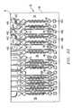
- FIG. 23shows a two-high module 10 devised in accordance with a preferred embodiment of the invention.
- FIG. 23has an area marked “A” that is subsequently shown in enlarged depiction in FIG. 24 .
- a form standard 35is shown disposed adjacent to upper surface 16 of CSP 14 .
- a form standard 35may be fixed to upper surface 16 of one or more of the CSPs in a module 10 with an adhesive 34 which preferably is thermally conductive.
- Form standard 35may also, in alternative embodiments, merely lay on upper surface 16 or be separated from upper surface 16 by an air gap or medium such as a thermal slug or non-thermal layer.
- Form standard 35is, in a preferred embodiment, devised from thermally conductive material such as, for example, copper to create, as shown in the depicted preferred embodiment of FIG. 23 , a mandrel that mitigates thermal accumulation while providing a standard sized form about which flex circuitry is disposed.
- Form standard 35may take other shapes and forms such as for example, an angular “cap” that rests upon the respective CSP body. It also need not be thermally enhancing although such attributes are preferable.
- the form standard 35allows the invention to be employed with CSPs of varying sizes, while articulating a single set of connective structures useable with the varying sizes of CSPs.
- a single set of connective structuressuch as flex circuits 30 and 32 (or a single flexible circuit in the mode where a single flex is used in place of the flex circuit pair 30 and 32 ) may be devised and used with the form standard 35 method and/or systems disclosed herein to create stacked modules with CSPs having different sized packages.
- Thiswill allow the same flexible circuitry set design to be employed to create iterations of a stacked module 10 from constituent CSPs having a first arbitrary dimension X across attribute Y (where Y may be, for example, package width), as well as modules 10 from constituent CSPs having a second arbitrary dimension X prime across that same attribute Y.
- CSPs of different sizesmay be stacked into modules 10 with the same set of connective structures (i.e. flex circuitry).
- portions of flex circuits 30 and 32are fixed to form standard 35 by adhesive 34 which is preferably a tape adhesive, but may be a liquid adhesive or may be placed in discrete locations across the package.
- adhesive 34is thermally conductive.
- flex circuits 30 and 32are multi-layer flexible circuit structures that have at least two conductive layers examples of which have been described earlier herein. Other embodiments may, however, employ flex circuitry, either as one circuit or two flex circuits to connect a pair of CSPs, that have only a single conductive layer.
- the conductive layersare metal such as alloy 110 .
- the use of plural conductive layersprovides advantages and the creation of a distributed capacitance across module 10 intended to reduce noise or bounce effects that can, particularly at higher frequencies, degrade signal integrity, as those of skill in the art will recognize.
- Module 10 of FIG. 23has plural module contacts 36 collectively identified as module array 38 . Appropriate fills such as those indicated earlier in FIG. 2 by conformal media reference 40 can provide added structural stability and coplanarity where desired.
- FIG. 23depicts in enlarged view, the area marked “A” in FIG. 23 .
- FIG. 24illustrates in a preferred embodiment, one arrangement of a form standard 35 and its relation to flex circuitry 30 in a two-high module 10 .
- the internal layer constructions of an exemplar flex circuitryhave been shown in earlier Figs.
- adhesive 34 between flex circuit 30 and form standard 34are also shown.
- adhesive 34is not required, but is preferred, and the site of its application may be determined as being best in the area between CSPs with a smaller amount near the terminal point of form standard 35 as shown in FIG. 24 .
- FIG. 24is an application of adhesive 34 between form standard 35 and CSP 14 .
- FIG. 25depicts an exemplar embodiment detail that illustrates use of flexible circuitry that employs a single conductive layer 64 .
- flex circuits 30 and 32extend further than shown and have portions which are, in the construction of module 10 brought about the curvature areas 66 of form standard 35 that mark the lateral extent of this example of a preferred form standard and are then disposed above the body of CSP 14 or the respective CSP of the module and therefore, the form standard.
- first and second outer layers 50 and 52 and intermediate layer 56are shown in this single conductive layer flex embodiment of module 10 .
- FIG. 25depicts an exemplar embodiment detail that illustrates use of flexible circuitry that employs a single conductive layer 64 .
- Form standard 35is shown attached to the body 27 of first level CSP 14 through an adhesive. In some embodiments, it may also be positioned to directly contact body 27 of the respective CSP. Form standard 35 may take many different configurations to allow a connective flex circuitry to be prepared exhibiting a single set of dimensions which may, when used in conjunction with form standard 35 , be employed to create stacked modules 10 from CSPs of a variety of different dimensions. In a preferred embodiment, form standard 35 will present a lateral extent broader than the upper major surface of the CSP over which it is disposed. Thus, the CSPs from one manufacturer may be aggregated into a stacked module 10 with the same flex circuitry used to aggregate CSPs from another manufacturer into a different stacked module 10 despite the CSPs from the two different manufacturers having different dimensions.
- heat transferencecan be improved with use of a form standard 35 comprised of heat transference material such as a metal, for example, or preferably, copper or a copper compound or alloy to provide a significant sink for thermal energy.
- a form standard 35comprised of heat transference material such as a metal, for example, or preferably, copper or a copper compound or alloy to provide a significant sink for thermal energy.
- thermal enhancement of module 10particularly presents opportunities for improvement of thermal performance where larger numbers of CSPs are aggregated in a single stacked module 10 .
Landscapes
- Engineering & Computer Science (AREA)
- Microelectronics & Electronic Packaging (AREA)
- Power Engineering (AREA)
- Physics & Mathematics (AREA)
- Condensed Matter Physics & Semiconductors (AREA)
- General Physics & Mathematics (AREA)
- Computer Hardware Design (AREA)
- Geometry (AREA)
- Semiconductor Memories (AREA)
- Design And Manufacture Of Integrated Circuits (AREA)
- Structure Of Printed Boards (AREA)
Abstract
Description
- This application is a continuation-in-part of U.S. patent application Ser. No. 10/400,309, filed Mar. 27, 2003, pending, which is a continuation of U.S. application Ser. No. 10/005,581, filed Oct. 26, 2001, now U.S. Pat. No. 6,576,992.
- This application is a continuation of U.S. patent application Ser. No. 10/814,530, filed Mar. 31, 2004, which is a continuation of U.S. patent application Ser. No. 10/453,398, filed Jun. 3, 2003, pending, which is a continuation-in-part of U.S. patent application Ser. No. 10/005,581, filed Oct. 26, 2001, now U.S. Pat. No. 6,576,992.
- The present invention relates to aggregating integrated circuits and, in particular, to stacking integrated circuits in chip-scale packages.
- A variety of techniques are used to stack packaged integrated circuits. Some methods require special packages, while other techniques stack conventional packages. In some stacks, the leads of the packaged integrated circuits are used to create a stack, while in other systems, added structures such as rails provide all or part of the interconnection between packages. In still other techniques, flexible conductors with certain characteristics are used to selectively interconnect packaged integrated circuits.
- The predominant package configuration employed during the past decade has encapsulated an integrated circuit (IC) in a plastic surround typically having a rectangular configuration. The enveloped integrated circuit is connected to the application environment through leads emergent from the edge periphery of the plastic encapsulation. Such “leaded packages” have been the constituent elements most commonly employed by techniques for stacking packaged integrated circuits.
- Leaded packages play an important role in electronics, but efforts to miniaturize electronic components and assemblies have driven development of technologies that preserve circuit board surface area. Because leaded packages have leads emergent from peripheral sides of the package, leaded packages occupy more than a minimal amount of circuit board surface area. Consequently, alternatives to leaded packages have recently gained market share.
- One family of alternative packages is identified generally by the term “chip scale packaging” or CSP. CSP refers generally to packages that provide connection to an integrated circuit through a set of contacts (often embodied as “bumps” or “balls”) arrayed across a major surface of the package. Instead of leads emergent from a peripheral side of the package, contacts are placed on a major surface and typically emerge from the planar bottom surface of the package.
- The goal of CSP is to occupy as little area as possible and, preferably, approximately the area of the encapsulated IC. Therefore, CSP leads or contacts do not typically extend beyond the outline perimeter of the package. The absence of “leads” on package sides renders most stacking techniques devised for leaded packages inapplicable for CSP stacking.
- CSP has enabled reductions in size and weight parameters for many applications. For example, micro ball grid array (μBGA) for flash and SRAM and wirebond on tape or rigid laminate CSPs for SRAM or EEPROM have been employed in a variety of applications. CSP is a broad category including a variety of packages from near chip scale to die-sized packages such as the die sized ball grid array (DSBGA) recently described in proposed JEDEC standard 95-1 for DSBGA.
- There are several known techniques for stacking packages articulated in chip scale technology. The assignee of the present invention has developed previous systems for aggregating μBGA packages in space saving topologies. The assignee of the present invention has systems for stacking BGA packages on a DIMM in a RAMBUS environment.
- In U.S. Pat. No. 6,205,654 B1 owned by the assignee of the present invention, a system for stacking ball grid array packages that employs lead carriers to extend connectable points out from the packages is described. Other known techniques add structures to a stack of BGA-packaged ICs. Still others aggregate CSPs on a DIMM with angular placement of the packages. Such techniques provide alternatives, but require topologies of added cost and complexity.
- The previous known methods for stacking CSPs apparently have various deficiencies including complex structural arrangements and thermal or high frequency performance issues.
- Thermal performance is a characteristic of importance in CSP stacks. To increase dissipation of heat generated by constituent CSPs, the thermal gradient between the lower CSP and upper CSP in a CSP stack or module should be minimized. Prior art solutions to CSP stacking do not, however, address thermal gradient minimization in disclosed constructions.
- What is needed, therefore, is a technique and system for stacking integrated circuits packaged in chip scale technology packaging that provides a thermally efficient, reliable structure that performs well at higher frequencies but does not add excessive height to the stack yet allows production at reasonable cost with readily understood and managed materials and methods.
- The present invention stacks chip scale-packaged integrated circuits (CSPs) into modules that conserve PWB or other board surface area. In a two-high CSP stack or module devised in accordance with a preferred embodiment of the present invention, two CSPs are stacked, with one CSP disposed above the other. The two CSPs are connected with flex circuitry. A form standard is disposed between the flex circuitry and a CSP in the stack. The form standard can take many configurations and may be used where flex circuits are used to connect CSPs to one another in stacked modules having two or more constituent ICs. For example, in stacked modules that include four CSPs, three form standards are employed in preferred embodiments, although fewer may be used. The form standard provides a physical form that allows many of the varying package sizes found in the broad family of CSP packages to be used to advantage while employing a standard connective flex circuitry design. In a preferred embodiment, the form standard will be devised of heat transference (thermally conductive) material.
FIG. 1 is an elevation view ofmodule 10 devised in accordance with a preferred embodiment of the present invention.FIG. 2 is an elevation view ofmodule 10 devised in accordance with a preferred embodiment of the present invention.FIG. 3 depicts, in enlarged view, the area marked “A” inFIG. 2 .FIG. 4 is an enlarged detail of an exemplar connection in a preferred embodiment of the present invention.FIG. 5 is an enlarged depiction of an exemplar area around a lower flex contact in a preferred embodiment of the present invention.FIG. 6 depicts a first outer surface layer of a flex circuit employed in a preferred embodiment of the present invention.FIG. 7 depicts a first outer surface layer of a flex circuit employed in a preferred embodiment of the present invention.FIG. 8 depicts a first conductive layer of a flex circuit employed in a preferred embodiment of the present invention.FIG. 9 illustrates a first conductive layer of a flex circuit employed in a preferred embodiment of the present invention.FIG. 10 depicts an intermediate layer of a flex circuit employed in a preferred embodiment of the present invention.FIG. 11 depicts an intermediate layer of a right side flex circuit employed in a preferred embodiment of the present invention.FIG. 12 depicts a second conductive layer of a flex circuit of a preferred embodiment of the present invention.FIG. 13 depicts a second conductive layer of a flex circuit of a preferred embodiment of the present invention.FIG. 14 depicts a second outer layer of a flex circuit employed in a preferred embodiment of the present invention.FIG. 15 reflects a second outer layer of a flex circuit employed in a preferred embodiment of the present invention.FIG. 16 depicts an alternative preferred embodiment of the present invention.FIG. 17 illustrates a JEDEC pinout for DDR-II FBGA packages.FIG. 18 illustrates the pinout of amodule 10 in an alternative preferred embodiment of the invention.FIG. 19 illustrates the pinout of amodule 10 in an alternative embodiment of the invention.FIG. 20 depicts the pinout of an exemplar CSP employed in a preferred embodiment of the invention.FIG. 21 depicts a second conductive layer of a flex circuit employed in an alternative preferred embodiment of the present invention.FIG. 22 depicts a second conductive layer of a flex circuit employed in an alternative preferred embodiment of the present invention.FIG. 23 depicts a module devised in accordance with a preferred embodiment of the present invention.FIG. 24 is an enlarged depiction of a portion of the embodiment depicted inFIG. 23 .FIG. 25 depicts a portion of a module devised in accordance with an alternative embodiment of the present invention.FIG. 1 is an elevation view ofmodule 10 devised in accordance with a preferred embodiment of the present invention.Module 10 is comprised ofupper CSP 12 andlower CSP 14. Each ofCSPs upper surface 16 and alower surface 18 and oppositelateral sides - The invention is used with CSP packages of a variety of types and configurations such as, for example, those that are die-sized, as well those that are near chip-scale as well as the variety of ball grid array packages known in the art. Collectively, these will be known herein as chip scale packaged integrated circuits (CSPs) and preferred embodiments will be described in terms of CSPs, but the particular configurations used in the explanatory figures are not, however, to be construed as limiting. For example, the elevation views of
FIGS. 1 and 2 are depicted with CSPs of a particular profile known to those in the art, but it should be understood that the figures are exemplary only. Later figures show embodiments of the invention that employ CSPs of other configurations as an example of one other of the many alternative CSP configurations with which the invention may be employed. The invention may be employed to advantage in the wide range of CSP configurations available in the art where an array of connective elements is emergent from at least one major surface. The invention is advantageously employed with CSPs that contain memory circuits but may be employed to advantage with logic and computing circuits where added capacity without commensurate PWB or other board surface area consumption is desired. - Typical CSPs, such as, for example, ball-grid-array (“BGA”), micro-ball-grid array (“μBGA”), and fine-pitch ball grid array (“FBGA”) packages have an array of connective contacts embodied, for example, as leads, bumps, solder balls, or balls that extend from
lower surface 18 of a plastic casing in any of several patterns and pitches. An external portion of the connective contacts is often finished with a ball of solder. Shown inFIG. 1 areCSP contacts 24 alonglower surfaces 18 ofCSPs CSP contacts 24 provide connection to the integrated circuit within the respective packages. Collectively,CSP contacts 24 compriseCSP array 26 shown as to lowerCSP 14 in the depicted particular package configuration asCSP arrays 26, and262 which collectively compriseCSP array 26. - In
FIG. 1 , flex circuits (“flex”, “flex circuits” or “flexible circuit structures”)30 and32 are shown partially wrapped aboutlower CSP 14 withflex 30 partially wrapped overlateral side 20 oflower CSP 14 and flex32 partially wrapped aboutlateral side 22 oflower CSP 14.Lateral sides lower CSP 14 and rigid in other areas for planarity along CSP surfaces may be employed as an alternative flex circuit in the present invention. For example, structures known as rigid-flex may be employed. - Portions of
flex circuits upper surface 16 oflower CSP 14 by adhesive34 which is shown as a tape adhesive, but may be a liquid adhesive or may be placed in discrete locations across the package. Preferably, adhesive34 is thermally conductive. Adhesives that include a flux are used to advantage in assembly ofmodule 10.Layer 34 may also be a thermally conductive medium to encourage heat flow between the CSPs ofmodule 10. Flex circuits module 10 intended to reduce noise or bounce effects that can, particularly at higher frequencies, degrade signal integrity, as those of skill in the art will recognize.Module 10 ofFIG. 1 hasmodule contacts 36 collectively identified asmodule array 38.FIG. 2 shows amodule 10 devised in accordance with a preferred embodiment of the invention.FIG. 2 illustrates use of aconformal media 40 provided in a preferred embodiment to assist in creating conformality of structural areas ofmodule 10. Planarity of the module is improved byconformal media 40. Preferably,conformal media 40 is thermally conductive. In alternative embodiments, thermal spreaders or a thermal medium may be placed as shown by reference41. Identified inFIG. 2 areupper flex contacts 42 andlower flex contacts 44 that are at one of the conductive layers offlex circuits Upper flex contacts 42 andlower flex contacts 44 are conductive material and, preferably, are solid metal.Lower flex contacts 44 are collectively lowerflex contact array 46.Upper flex contacts 42 are collectively upperflex contact array 48. Only some ofupper flex contacts 42 andlower flex contacts 44 are identified inFIG. 2 to preserve clarity of the view. It should be understood that each offlex circuits upper flex contacts 42 andlower flex contacts 44.Lower flex contacts 44 are employed withlower CSP 14 andupper flex contacts 42 are employed withupper CSP 12.FIG. 2 has an area marked “A” that is subsequently shown in enlarged depiction inFIG. 3 .FIG. 3 depicts in enlarged view, the area marked “A” inFIG. 2 .FIG. 3 illustrates the connection betweenexample CSP contact 24 andmodule contact 36 throughlower flex contact 44 to illustrate the solid metal path fromlower CSP 14 tomodule contact 36 and, therefore, to an application PWB to which module is connectable. As those of skill in the art will understand, heat transference frommodule 10 is thereby encouraged.- With continuing reference to
FIG. 3 ,CSP contact 24 andmodule contact 36 together offsetmodule 10 from an application platform such as a PWB. The combined heights ofCSP contact 24 andmodule contact 36 provide a moment arm longer than the height of asingle CSP contact 24 alone. This provides a longer moment arm through which temperature-gradient-over-time stresses (such as typified by temp cycle), can be distributed. Flex 30 is shown inFIG. 3 to be comprised of multiple layers.Flex 30 has a firstouter surface 50 and a secondouter surface 52.Flex circuit 30 has at least two conductive layers interior to first and secondouter surfaces flex 30 andflex 32. In the depicted preferred embodiment, firstconductive layer 54 and secondconductive layer 58 are interior to first and secondouter surfaces Intermediate layer 56 lies between firstconductive layer 54 and secondconductive layer 58. There may be more than one intermediate layer, but one intermediate layer of polyimide is preferred.- As depicted in
FIG. 3 and seen in more detail in later figures,lower flex contact 44 is preferably comprised from metal at the level of secondconductive layer 58 interior to secondouter surface 52.Lower flex contact 44 is solid metal in a preferred embodiment and is comprised of metal alloy such as alloy110. This results in a solid metal pathway fromlower CSP 14 to an application board thereby providing a significant thermal pathway for dissipation of heat generated inmodule 10. FIG. 4 is an enlarged detail of an exemplar connection betweenexample CSP contact 24 andexample module contact 36 throughlower flex contact 44 to illustrate the solid metal path fromlower CSP 14 tomodule contact 36 and, therefore, to an application PWB to whichmodule 10 is connectable. As shown inFIG. 4 ,lower flex contact 44 is at secondconductive layer 58 that is interior to first and second outer surface layers50 and52 respectively, offlex circuit 30.FIG. 5 is an enlarged depiction of an exemplar area around alower flex contact 44 in a preferred embodiment.Windows lower flex contacts 44 residing at the level of secondconductive layer 58 in the flex. Theupper flex contacts 42 are contacted byCSP contacts 24 ofupper CSP 12.Lower flex contacts 44 andupper flex contacts 42 are particular areas of conductive material (preferably metal such as alloy110) at the level of secondconductive layer 58 in the flex.Upper flex contacts 42 andlower flex contacts 44 are demarked in secondconductive layer 58 and, as will be shown in subsequent Figs., may be connected to or isolated from the conductive plane of secondconductive layer 58. Demarking alower flex contact 44 from secondconductive layer 58 is represented inFIG. 5 bydemarcation gap 63 shown at secondconductive layer 58. Where an upper orlower flex contact conductive layer 58, demarcation gaps do not extend completely around the flex contact as shown, for example, bylower flex contacts 44C in laterFIG. 12 .CSP contacts 24 oflower CSP 14 pass through awindow 60 opened through firstouter surface layer 50, firstconductive layer 54, andintermediate layer 56, to contact an appropriatelower flex contact 44.Window 62 is opened through secondouter surface layer 52 through whichmodule contacts 36 pass to contact the appropriatelower flex contact 44.- Respective ones of
CSP contacts 24 ofupper CSP 12 andlower CSP 14 are connected at the secondconductive layer 58 level inflex circuits Respective CSP contacts 24 ofupper CSP 12 andlower CSP 14 that convey ground (VSS) signals are connected at the firstconductive layer 54 level inflex circuits intermediate layer 56 to connect the levels as will subsequently be described in further detail. Thereby,CSPs flex circuits lower CSP 14,respective CSP contacts 24 of each of upper andlower CSPs lower flex contacts upper flex contacts 42 andlower flex contacts 44 are connected. Consequently, by being in contact withlower flex contacts 44,module contacts 36 are in contact with both upper andlower CSPs - In a preferred embodiment,
module contacts 36 pass throughwindows 62 opened in secondouter layer 52 to contactlower CSP contacts 44. In some embodiments, as will be later shown,module 10 will exhibit amodule contact array 38 that has a greater number of contacts than do the constituent CSPs ofmodule 10. In such embodiments, some ofmodule contacts 36 may contactlower flex contacts 44 that do not contact one of theCSP contacts 24 oflower CSP 14 but are connected toCSP contacts 24 ofupper CSP 12. This allowsmodule 10 to express a wider datapath than that expressed by theconstituent CSPs module contact 36 may also be in contact with alower flex contact 44 to provide a location through which different levels of CSPs in the module may be enabled when no unused CSP contacts are available or convenient for that purpose. - In a preferred embodiment, first
conductive layer 54 is employed as a ground plane, while secondconductive layer 58 provides the functions of being a signal conduction layer and a voltage conduction layer. Those of skill will note that roles of the first and second conductive layers may be reversed with attendant changes in windowing and use of commensurate interconnections. - As those of skill will recognize, interconnection of respective
voltage CSP contacts 24 of upper andlower CSPs module 10. Such flattening of the thermal gradient curve acrossmodule 10 is further encouraged by connection of commonground CSP contacts 24 of upper andlower CSPs conductive layer 54. Those of skill will notice that between first and secondconductive layers intermediate layer 56 that, in a preferred embodiment, is a polyimide. Placement of such an intermediate layer between ground-conductive firstconductive layer 54 and signal/voltage conductive secondconductive layer 58 provides, in the combination, a distributed capacitance that assists in mitigation of ground bounce phenomena to improve high frequency performance ofmodule 10. - In a preferred embodiment,
FIG. 6 depicts firstouter surface layer 50 of flex30 (i.e., left side ofFIG. 1 ). The view is from above the flex looking down intoflex 30 from the perspective of firstconductive layer 54. Throughout the Figs., the location reference “B” is to orient views of layers offlex 30 to those offlex 32 as well as across layers.Windows 60 are opened through firstouter surface layer 50, firstconductive layer 54, andintermediate layer 56.CSP contacts 24 oflower CSP 14 pass throughwindows 60 of firstouter surface layer 50, firstconductive layer 54, andintermediate layer 56 to reach the level of secondconductive layer 58 offlex 30. At secondconductive layer 58, selectedCSP contacts 24 oflower CSP 14 make contact with selectedlower flex contacts 44.Lower flex contacts 44 provide several types of connection in a preferred embodiment as will be explained with reference to laterFIG. 12 . Whenmodule 10 is assembled, a portion offlex 30 will be wrapped aboutlateral side 20 oflower CSP 14 to placeedge 62 aboveupper surface 16 oflower CSP 14. - In a preferred embodiment,
FIG. 7 depicts firstouter surface layer 50 of flex32 (i.e., right side ofFIG. 1 ). The view is from above the flex looking down intoflex 32 from the perspective of firstconductive layer 54. The location reference “B” relatively orients the views ofFIGS. 6 and 7 . The views ofFIGS. 6 and 7 may be understood together with the reference marks “B” of each view being placed nearer each other than to any other corner of the other view of the pair of views of the same layer. As shown inFIG. 7 ,windows 60 are opened through firstouter surface layer 50, firstconductive layer 54 andintermediate layer 56.CSP contacts 24 oflower CSP 14 pass throughwindows 60 of firstouter surface layer 50, firstconductive layer 54, andintermediate layer 56 to reach the level of secondconductive layer 58 offlex 30. At secondconductive layer 58, selectedCSP contacts 24 oflower CSP 14 make contact withlower flex contacts 44.Lower flex contacts 44 provide several types of connection in a preferred embodiment as will be explained with reference to laterFIG. 12 . Whenmodule 10 is assembled, a portion offlex 32 will be wrapped aboutlateral side 22 oflower CSP 14 to placeedge 64 aboveupper surface 16 oflower CSP 14. FIG. 8 depicts firstconductive layer 54 offlex 30.Windows 60 continue the opened orifice inflex 30 through whichCSP contacts 24 oflower CSP 14 pass to reach secondconductive layer 58 and, therefore, selectedlower flex contacts 44 at the level of secondconductive layer 58.- Those of skill will recognize that as
flex 30 is partially wrapped aboutlateral side 20 oflower CSP 14, firstconductive layer 54 becomes, on the part offlex 30 disposed aboveupper surface 16 oflower CSP 14, the lower-most conductive layer offlex 30 from the perspective ofupper CSP 12. In the depicted embodiment, thoseCSP contacts 24 ofupper CSP 12 that provide ground (VSS) connections are connected to the firstconductive layer 54. Firstconductive layer 54 lies beneath, however, secondconductive layer 58 in that part offlex 30 that is wrapped abovelower CSP 14. Consequently, some means must be provided for connection of theupper flex contact 42 to which ground-conveyingCSP contacts 24 ofupper CSP 12 are connected and firstconductive layer 54. Consequently, in the depicted preferred embodiment, thoseupper flex contacts 42 that are in contact with ground-conveyingCSP contacts 24 ofupper CSP 12 have vias that route throughintermediate layer 56 to reach firstconductive layer 54. The sites where those vias meet firstconductive layer 54 are identified inFIG. 8 asvias 66. These vias may be “on-pad” or coincident with theflex contact 42 to which they are connected. Those of skill will note a match between the vias66 identified inFIG. 8 and vias66 identified in the later view of secondconductive layer 58 of the depicted preferred embodiment. In a preferred embodiment, vias66 in coincident locations from Fig. to Fig. are one via. For clarity of the view, depicted vias in the figures are shown larger in diameter than in manufactured embodiments. As those of skill will recognize, the connection between conductive layers provided by vias (on or off pad) may be provided any of several well-known techniques such as plated holes or solid lines or wires and need not literally be vias. - Also shown in
FIG. 8 are off-pad vias 74. Off-pad vias 74 are disposed on firstconductive layer 54 at locations near, but not coincident with selected ones ofwindows 60. Unlikevias 66 that connect selected ones ofupper flex contacts 42 to firstconductive layer 54, off-pad vias 74 connect selected ones oflower flex contacts 44 to firstconductive layer 54. In the vicinity ofupper flex contacts 42, secondconductive layer 58 is between the CSP connected tomodule 10 by the upper flex contacts42 (i.e., upper CSP12) and firstconductive layer 54. Consequently, vias between ground-conveyingupper flex contacts 42 and firstconductive layer 54 may be directly attached to the selectedupper flex contacts 42 through which ground signals are conveyed. In contrast, in the vicinity oflower flex contacts 44, firstconductive layer 54 is between the CSP connected tomodule 10 by the lower flex contacts44 (i.e., lower CSP14) and secondconductive layer 58. Consequently, vias between ground-conveyinglower flex contacts 44 and firstconductive layer 54 are offset from the selectedlower flex contacts 44 by off-pad vias 74 shown in offset locations. FIG. 9 illustrates firstconductive layer 54 offlex 32. The location reference marks “B” are employed to relatively orientFIGS. 8 and 9 .Windows 60, vias66 and off-pad vias 74 are identified inFIG. 9 . Also shown inFIG. 9 , are enablevias trace 72. Enable via70 is connected off-pad to a selectedlower flex contact 44 that corresponds, in this preferred embodiment, to anunused CSP contact 24 of lower CSP14 (i.e., a N/C). Amodule contact 36 at that site conveys an enable signal (C/S) forupper CSP 12 through the selected lower flex contact44 (which is at the level of second conductive layer58) to off-pad enable via70 that conveys the enable signal to firstconductive layer 54 and thereby to enabletrace 72. Enabletrace 72 further conveys the enable signal to enable via68 which extends throughintermediate layer 56 to selectedupper flex contact 42 at the level of secondconductive layer 58 where contact is made with the C/S pin ofupper CSP 12. Thus, upper andlower CSPs FIG. 10 depictsintermediate layer 56 offlex 30.Windows 60 are shown opened inintermediate surface 56.CSP contacts 24 oflower CSP 14 pass throughwindows 60 inintermediate layer 58 to reachlower flex contacts 44 at the level of secondconductive layer 58. Those of skill will notice that, in the depicted preferred embodiment,windows 60 narrow in diameter from their manifestation in firstouter layer 50.Vias 66, off-pad vias 74, and enablevias intermediate layer 56 connecting selected conductive areas at the level of first and secondconductive layers FIG. 11 depictsintermediate layer 56 offlex 32 showingwindows 60, vias66, off-pad vias 74, and enablevias intermediate layer 56.FIG. 12 depicts secondconductive layer 58 offlex 30 of a preferred embodiment of the present invention. Depicted are various types ofupper flex contacts 42, various types oflower flex contacts 44, signal traces76, andVDD plane 78 as well as previously describedvias 66 and off-pad vias 74. ThroughoutFIGS. 12 and 13 , only exemplars of particular features are identified to preserve clarity of the view.Flex contacts 44A are connected to corresponding selectedupper flex contacts 42A with signal traces76. To enhance the clarity of the view, only exemplarindividual flex contacts FIG. 12 . As shown, in this preferred embodiment, signal traces76 exhibit path routes determined to provide substantially equal signal lengths betweencorresponding flex contacts conductive layer 58 that is identified asVDD plane 78.VDD plane 78 may be in one or more delineated sections but, preferably is one section.Lower flex contacts 44C provide connection toVDD plane 78. In a preferred embodiment,upper flex contacts 42C andlower flex contacts 44C connectupper CSP 12 andlower CSP 14, respectively, toVDD plane 78.Lower flex contacts 44 that are connected to firstconductive layer 54 by off-pad vias 74 are identified aslower flex contacts 44B. To enhance the clarity of the view, only exemplar individuallower flex contacts 44B are literally identified inFIG. 12 .Upper flex contacts 42 that are connected to firstconductive layer 54 byvias 66 are identified asupper flex contacts 42B.FIG. 13 depicts secondconductive layer 58 ofright side flex 32 of a preferred embodiment of the present invention. Depicted are various types ofupper flex contacts 42, various types oflower flex contacts 44, signal traces76, andVDD plane 78 as well as previously describedvias 66, off-pad vias 74, and enablevias FIG. 13 illustratesupper flex contacts 42A connected bytraces 76 tolower flex contacts 44A.VDD plane 78 provides a voltage plane at the level of secondconductive layer 58.Lower flex contacts 44C andupper flex contacts 42C connectlower CSP 14 andupper CSP 12, respectively, toVDD plane 78.Lower flex contact 44D is shown with enable via70 described earlier. Correspondingupper flex contact 42D is connected tolower flex contact 44D through enablevias trace 72 at the firstconductive layer 54 level offlex 32.FIG. 14 depicts secondouter layer 52 offlex 30.Windows 62 are identified. Those of skill will recognize thatmodule contacts 36 pass throughwindows 62 to contact appropriatelower flex contacts 44. Whenflex 30 is partially wrapped aboutlateral side 20 oflower CSP 14, a portion of secondouter layer 52 becomes the upper-most layer offlex 30 from the perspective ofupper CSP 12.CSP contacts 24 ofupper CSP 12 pass throughwindows 64 to reach secondconductive layer 58 and make contact with appropriate ones ofupper flex contacts 42 located at that level.FIG. 15 reflects secondouter layer 52 offlex 32 andexhibits windows Module contacts 36 pass throughwindows 62 to contact appropriatelower flex contacts 44.CSP contacts 24 ofupper CSP 12 pass throughwindows 64 to reach secondconductive layer 58 and make contact with appropriate ones ofupper flex contacts 42 located at that level.FIG. 16 depicts an alternative preferred embodiment of the presentinvention showing module 10. Those of skill will recognize that the embodiment depicted inFIG. 16 differs from that inFIG. 2 by the presence ofmodule contacts 36E.Module contacts 36E supply a part of the datapath ofmodule 10 and may provide a facility for differential enablement of the constituent CSPs. Amodule contact 36E not employed in wide datapath provision may provide a contact point to supply an enable signal to differentially enableupper CSP 12 orlower CSP 14.- In a
wide datapath module 10, the data paths of the constituentupper CSP 12 andlower CSP 14 are combined to provide amodule 10 that expresses a module datapath that is twice the width of the datapaths of the constituent CSPs in a two-high module 10. The preferred method of combination is concatenation, but other combinations may be employed to combine the datapaths ofCSPs module contacts - As an example,
FIGS. 17, 18 , and19 are provided to illustrate using addedmodule contacts 36E in alternative embodiments of the present invention to provide wider datapaths formodule 10 than are present inconstituent CSPs FIG. 17 illustrates a JEDEC pinout for DDR-II FBGA packages.FIG. 18 illustrates the pinout provided bymodule contacts module 10 expressing an 8-bit wide datapath.Module 10 is devised in accordance with the present invention and is, in the exemplar embodiment, comprised of anupper CSP 12 andlower CSP 14 that are DDR-II-compliant in timing, but each of which are only 4 bits wide in datapath. As will be recognized, themodule 10 mapped inFIG. 18 expresses an 8-bit wide datapath. For example,FIG. 18 depicts DQ pins differentiated in source between upper CSP12 (“top”) and lower CSP14 (“bot”) to aggregate to 8-bits.FIG. 19 illustrates the pinout provided bymodule contacts module 10 expressing a 16-bit wide datapath.Module 10 is devised in accordance with the present invention and is, in this exemplar embodiment, comprised of anupper CSP 12 andlower CSP 14 that are DDR-II-compliant in timing, but each of which are only 8-bits wide in datapath. Those of skill in the art will recognize that the wide datapath embodiment may be employed with any of a variety of CSPs available in the field and such CSPs need not be DDR compliant. FIG. 20 illustrates a typical pinout of a memory circuit provided as a CSP and useable in the present invention. Individual array positions are identified by the JEDEC convention of numbered columns and alphabetic rows. The central area (e.g., A3-A6; B3-B6; etc.) is unpopulated.CSP contacts 24 are present at the locations that are identified by alpha-numeric identifiers such as, for example, A3, shown as anexample CSP contact 24.FIG. 21 depictssecond metal layer 58 offlex 30 in an alternative embodiment of the invention in whichmodule 10 expresses a datapath wider than that expressed by either of the theconstituent CSPs Lower flex contacts 44E are not contacted byCSP contacts 24 oflower CSP 14, but are contacted bymodule contacts 36E to provide, with selectedmodule contacts 36, a datapath formodule 10 that is 2n-bits in width where the datapaths ofCSPs FIG. 21 ,lower flex contacts 44E are connected toupper flex contacts 42E. As shown in earlierFIG. 14 ,windows 62 pass through secondouter layer 52. In the alternative preferred embodiment for which secondconductive layer 58 is shown inFIG. 21 ,module contacts windows 62 in secondouter layer 52 offlex circuit 30, to contact appropriatelower flex contacts 44.FIG. 22 illustratessecond metal layer 58 offlex 32 in an alternative embodiment of the invention in whichmodule 10 expresses a datapath wider than that expressed by either of the theconstituent CSPs Lower flex contacts 44E are not contacted byCSP contacts 24 oflower CSP 14, but are contacted bymodule contacts 36E to provide, with selectedmodule contacts 36, a datapath formodule 10 that is 2n-bits in width where the datapaths ofCSPs FIG. 22 ,lower flex contacts 44E are connected toupper flex contacts 42E. As shown in earlierFIG. 14 ,windows 62 pass through secondouter layer 52. In the alternative preferred embodiment for which secondconductive layer 58 is shown inFIG. 22 ,module contacts 36 pass throughwindows 62 in secondouter layer 52 offlex circuit 32, to contact appropriatelower flex contacts 44.- In particular, in the embodiment depicted in
FIGS. 21 and 22 ,module contacts 36Econtact flex contacts 44E and44EE. Those of skill will recognize thatlower flex contacts 44E are, in the depicted embodiment, eight (8) in number and that there is another lower flex contacts identified by reference44EE shown onFIG. 21 . Lower flex contact44EE is contacted by one of themodule contacts 36E to provide differential enablement between upper and lower CSPs. Those of skill will recognize thatlower flex contacts 44E are connected to correspondingupper flex contacts 42E.CSP contacts 24 ofupper CSP 12 that convey data are in contact withupper flex contacts 42E. Consequently, the datapaths of bothupper CSP 12 andlower CSP 14 are combined to provide a wide datapath onmodule 10. With the depicted connections ofFIGS. 21 and 22 ,lower flex contacts 44E offlex circuits module contacts 36E, the datapath ofupper CSP 12, while otherlower flex contacts 44 convey the datapath oflower CSP 14 tomodule contacts 36 to providemodule 10 with a module datapath that is the combination of the datapath ofupper CSP 12 andlower CSP 14. In the depicted particular embodiment ofFIGS. 21 and 22 ,module 10 expresses a 16-bit datapath andCSP 12 andCSP 14 each express an 8-bit datapath. FIG. 23 shows a two-high module 10 devised in accordance with a preferred embodiment of the invention.FIG. 23 has an area marked “A” that is subsequently shown in enlarged depiction inFIG. 24 . With reference toFIG. 23 , aform standard 35 is shown disposed adjacent toupper surface 16 ofCSP 14. Aform standard 35 may be fixed toupper surface 16 of one or more of the CSPs in amodule 10 with an adhesive34 which preferably is thermally conductive. Form standard35 may also, in alternative embodiments, merely lay onupper surface 16 or be separated fromupper surface 16 by an air gap or medium such as a thermal slug or non-thermal layer.- Form standard35 is, in a preferred embodiment, devised from thermally conductive material such as, for example, copper to create, as shown in the depicted preferred embodiment of
FIG. 23 , a mandrel that mitigates thermal accumulation while providing a standard sized form about which flex circuitry is disposed. Form standard35 may take other shapes and forms such as for example, an angular “cap” that rests upon the respective CSP body. It also need not be thermally enhancing although such attributes are preferable. Theform standard 35 allows the invention to be employed with CSPs of varying sizes, while articulating a single set of connective structures useable with the varying sizes of CSPs. Thus, a single set of connective structures such asflex circuits 30 and32 (or a single flexible circuit in the mode where a single flex is used in place of theflex circuit pair 30 and32) may be devised and used with the form standard35 method and/or systems disclosed herein to create stacked modules with CSPs having different sized packages. This will allow the same flexible circuitry set design to be employed to create iterations of a stackedmodule 10 from constituent CSPs having a first arbitrary dimension X across attribute Y (where Y may be, for example, package width), as well asmodules 10 from constituent CSPs having a second arbitrary dimension X prime across that same attribute Y. Thus, CSPs of different sizes may be stacked intomodules 10 with the same set of connective structures (i.e. flex circuitry). - Preferably, portions of
flex circuits - In a preferred embodiment,
flex circuits - Preferably, the conductive layers are metal such as alloy110. The use of plural conductive layers provides advantages and the creation of a distributed capacitance across
module 10 intended to reduce noise or bounce effects that can, particularly at higher frequencies, degrade signal integrity, as those of skill in the art will recognize.Module 10 ofFIG. 23 hasplural module contacts 36 collectively identified asmodule array 38. Appropriate fills such as those indicated earlier inFIG. 2 byconformal media reference 40 can provide added structural stability and coplanarity where desired. FIG. 23 depicts in enlarged view, the area marked “A” inFIG. 23 .FIG. 24 illustrates in a preferred embodiment, one arrangement of aform standard 35 and its relation to flexcircuitry 30 in a two-high module 10. The internal layer constructions of an exemplar flex circuitry have been shown in earlier Figs. Also shown is adhesive34 betweenflex circuit 30 and form standard34. Those of skill will note that adhesive34 is not required, but is preferred, and the site of its application may be determined as being best in the area between CSPs with a smaller amount near the terminal point of form standard35 as shown inFIG. 24 . Also shown inFIG. 24 is an application of adhesive34 between form standard35 andCSP 14.FIG. 25 depicts an exemplar embodiment detail that illustrates use of flexible circuitry that employs a singleconductive layer 64. It should be understood with reference toFIG. 25 thatflex circuits module 10 brought about thecurvature areas 66 of form standard35 that mark the lateral extent of this example of a preferred form standard and are then disposed above the body ofCSP 14 or the respective CSP of the module and therefore, the form standard. In this single conductive layer flex embodiment ofmodule 10, there are shown first and secondouter layers intermediate layer 56. Also shown inFIG. 25 are a set of single layerlower flex contacts 68 demarked at the level ofconductive layer 64.- Form standard35 is shown attached to the
body 27 offirst level CSP 14 through an adhesive. In some embodiments, it may also be positioned to directly contactbody 27 of the respective CSP. Form standard35 may take many different configurations to allow a connective flex circuitry to be prepared exhibiting a single set of dimensions which may, when used in conjunction with form standard35, be employed to createstacked modules 10 from CSPs of a variety of different dimensions. In a preferred embodiment, form standard35 will present a lateral extent broader than the upper major surface of the CSP over which it is disposed. Thus, the CSPs from one manufacturer may be aggregated into astacked module 10 with the same flex circuitry used to aggregate CSPs from another manufacturer into a differentstacked module 10 despite the CSPs from the two different manufacturers having different dimensions. - Further, heat transference can be improved with use of a form standard35 comprised of heat transference material such as a metal, for example, or preferably, copper or a copper compound or alloy to provide a significant sink for thermal energy. Such thermal enhancement of
module 10 particularly presents opportunities for improvement of thermal performance where larger numbers of CSPs are aggregated in a single stackedmodule 10. - Although the present invention has been described in detail, it will be apparent to those skilled in the art that the invention may be embodied in a variety of specific forms and that various changes, substitutions and alterations can be made without departing from the spirit and scope of the invention. The described embodiments are only illustrative and not restrictive and the scope of the invention is, therefore, indicated by the following claims.
Claims (41)
Priority Applications (1)
| Application Number | Priority Date | Filing Date | Title |
|---|---|---|---|
| US11/197,267US7495334B2 (en) | 2001-10-26 | 2005-08-04 | Stacking system and method |
Applications Claiming Priority (5)
| Application Number | Priority Date | Filing Date | Title |
|---|---|---|---|
| US10/005,581US6576992B1 (en) | 2001-10-26 | 2001-10-26 | Chip scale stacking system and method |
| US10/400,309US20030137048A1 (en) | 2001-10-26 | 2003-03-27 | Stacking system and method |
| US10/453,398US6914324B2 (en) | 2001-10-26 | 2003-06-03 | Memory expansion and chip scale stacking system and method |
| US10/814,530US20040178496A1 (en) | 2001-10-26 | 2004-03-31 | Memory expansion and chip scale stacking system and method |
| US11/197,267US7495334B2 (en) | 2001-10-26 | 2005-08-04 | Stacking system and method |
Related Parent Applications (2)
| Application Number | Title | Priority Date | Filing Date |
|---|---|---|---|
| US10/400,309Continuation-In-PartUS20030137048A1 (en) | 2001-10-26 | 2003-03-27 | Stacking system and method |
| US10/814,530ContinuationUS20040178496A1 (en) | 2001-10-26 | 2004-03-31 | Memory expansion and chip scale stacking system and method |
Related Child Applications (1)
| Application Number | Title | Priority Date | Filing Date |
|---|---|---|---|
| US10/453,398Continuation-In-PartUS6914324B2 (en) | 2001-10-26 | 2003-06-03 | Memory expansion and chip scale stacking system and method |
Publications (2)
| Publication Number | Publication Date |
|---|---|
| US20050280135A1true US20050280135A1 (en) | 2005-12-22 |
| US7495334B2 US7495334B2 (en) | 2009-02-24 |
Family
ID=33489536
Family Applications (6)
| Application Number | Title | Priority Date | Filing Date |
|---|---|---|---|
| US10/453,398Expired - LifetimeUS6914324B2 (en) | 2001-10-26 | 2003-06-03 | Memory expansion and chip scale stacking system and method |
| US10/814,530AbandonedUS20040178496A1 (en) | 2001-10-26 | 2004-03-31 | Memory expansion and chip scale stacking system and method |
| US10/709,732Expired - LifetimeUS6955945B2 (en) | 2001-10-26 | 2004-05-25 | Memory expansion and chip scale stacking system and method |
| US10/963,867Expired - Fee RelatedUS7256484B2 (en) | 2001-10-26 | 2004-10-12 | Memory expansion and chip scale stacking system and method |
| US10/978,149AbandonedUS20050067683A1 (en) | 2001-10-26 | 2004-10-29 | Memory expansion and chip scale stacking system and method |
| US11/197,267Expired - LifetimeUS7495334B2 (en) | 2001-10-26 | 2005-08-04 | Stacking system and method |
Family Applications Before (5)
| Application Number | Title | Priority Date | Filing Date |
|---|---|---|---|
| US10/453,398Expired - LifetimeUS6914324B2 (en) | 2001-10-26 | 2003-06-03 | Memory expansion and chip scale stacking system and method |
| US10/814,530AbandonedUS20040178496A1 (en) | 2001-10-26 | 2004-03-31 | Memory expansion and chip scale stacking system and method |
| US10/709,732Expired - LifetimeUS6955945B2 (en) | 2001-10-26 | 2004-05-25 | Memory expansion and chip scale stacking system and method |
| US10/963,867Expired - Fee RelatedUS7256484B2 (en) | 2001-10-26 | 2004-10-12 | Memory expansion and chip scale stacking system and method |
| US10/978,149AbandonedUS20050067683A1 (en) | 2001-10-26 | 2004-10-29 | Memory expansion and chip scale stacking system and method |
Country Status (3)
| Country | Link |
|---|---|
| US (6) | US6914324B2 (en) |
| AU (1) | AU2003304192A1 (en) |
| WO (1) | WO2004109802A1 (en) |
Cited By (4)
| Publication number | Priority date | Publication date | Assignee | Title |
|---|---|---|---|---|
| US20050116330A1 (en)* | 2003-11-11 | 2005-06-02 | Rina Murayama | Semiconductor module and method for mounting the same |
| US20080048309A1 (en)* | 2006-08-28 | 2008-02-28 | Corisis David J | Metal core foldover package structures, systems including same and methods of fabrication |
| US7888185B2 (en) | 2006-08-17 | 2011-02-15 | Micron Technology, Inc. | Semiconductor device assemblies and systems including at least one conductive pathway extending around a side of at least one semiconductor device |
| US20220077014A1 (en)* | 2019-07-09 | 2022-03-10 | Texas Instruments Incorporated | Packaged device with die wrapped by a substrate |
Families Citing this family (121)
| Publication number | Priority date | Publication date | Assignee | Title |
|---|---|---|---|---|
| US5484959A (en)* | 1992-12-11 | 1996-01-16 | Staktek Corporation | High density lead-on-package fabrication method and apparatus |
| US6551857B2 (en)* | 1997-04-04 | 2003-04-22 | Elm Technology Corporation | Three dimensional structure integrated circuits |
| US5915167A (en)* | 1997-04-04 | 1999-06-22 | Elm Technology Corporation | Three dimensional structure memory |
| US6323060B1 (en) | 1999-05-05 | 2001-11-27 | Dense-Pac Microsystems, Inc. | Stackable flex circuit IC package and method of making same |
| US6262895B1 (en) | 2000-01-13 | 2001-07-17 | John A. Forthun | Stackable chip package with flex carrier |
| KR100964482B1 (en)* | 2001-02-28 | 2010-06-21 | 데이톤 시스템즈 그룹 인코포레이티드 | Method and apparatus for forming the container end |
| US7053478B2 (en) | 2001-10-26 | 2006-05-30 | Staktek Group L.P. | Pitch change and chip scale stacking system |
| US6956284B2 (en) | 2001-10-26 | 2005-10-18 | Staktek Group L.P. | Integrated circuit stacking system and method |
| US7371609B2 (en) | 2001-10-26 | 2008-05-13 | Staktek Group L.P. | Stacked module systems and methods |
| US20060255446A1 (en) | 2001-10-26 | 2006-11-16 | Staktek Group, L.P. | Stacked modules and method |
| US7485951B2 (en)* | 2001-10-26 | 2009-02-03 | Entorian Technologies, Lp | Modularized die stacking system and method |
| US6576992B1 (en)* | 2001-10-26 | 2003-06-10 | Staktek Group L.P. | Chip scale stacking system and method |
| US7202555B2 (en) | 2001-10-26 | 2007-04-10 | Staktek Group L.P. | Pitch change and chip scale stacking system and method |
| US6914324B2 (en) | 2001-10-26 | 2005-07-05 | Staktek Group L.P. | Memory expansion and chip scale stacking system and method |
| US7656678B2 (en) | 2001-10-26 | 2010-02-02 | Entorian Technologies, Lp | Stacked module systems |
| US7026708B2 (en)* | 2001-10-26 | 2006-04-11 | Staktek Group L.P. | Low profile chip scale stacking system and method |
| US20030234443A1 (en) | 2001-10-26 | 2003-12-25 | Staktek Group, L.P. | Low profile stacking system and method |
| US20050056921A1 (en)* | 2003-09-15 | 2005-03-17 | Staktek Group L.P. | Stacked module systems and methods |
| US6940729B2 (en) | 2001-10-26 | 2005-09-06 | Staktek Group L.P. | Integrated circuit stacking system and method |
| US20040195666A1 (en)* | 2001-10-26 | 2004-10-07 | Julian Partridge | Stacked module systems and methods |
| US20050009234A1 (en)* | 2001-10-26 | 2005-01-13 | Staktek Group, L.P. | Stacked module systems and methods for CSP packages |
| US7310458B2 (en) | 2001-10-26 | 2007-12-18 | Staktek Group L.P. | Stacked module systems and methods |
| US7081373B2 (en) | 2001-12-14 | 2006-07-25 | Staktek Group, L.P. | CSP chip stack with flex circuit |
| US6639309B2 (en) | 2002-03-28 | 2003-10-28 | Sandisk Corporation | Memory package with a controller on one side of a printed circuit board and memory on another side of the circuit board |
| US20050021470A1 (en)* | 2002-06-25 | 2005-01-27 | Bose Corporation | Intelligent music track selection |
| US8111132B2 (en)* | 2004-01-06 | 2012-02-07 | Bose Corporation | Remote controlling |
| US20030236582A1 (en)* | 2002-06-25 | 2003-12-25 | Lee Zamir | Selection of items based on user reactions |
| AU2003255254A1 (en)* | 2002-08-08 | 2004-02-25 | Glenn J. Leedy | Vertical system integration |
| US20040245615A1 (en)* | 2003-06-03 | 2004-12-09 | Staktek Group, L.P. | Point to point memory expansion system and method |
| US7612443B1 (en) | 2003-09-04 | 2009-11-03 | University Of Notre Dame Du Lac | Inter-chip communication |
| US7542304B2 (en) | 2003-09-15 | 2009-06-02 | Entorian Technologies, Lp | Memory expansion and integrated circuit stacking system and method |
| US20050150813A1 (en)* | 2003-10-29 | 2005-07-14 | Tessera, Inc. | Foldover packages and manufacturing and test methods therefor |
| US8250295B2 (en)* | 2004-01-05 | 2012-08-21 | Smart Modular Technologies, Inc. | Multi-rank memory module that emulates a memory module having a different number of ranks |
| US7111080B2 (en)* | 2004-03-01 | 2006-09-19 | Cisco Technology, Inc. | Distributing an electronic signal in a stackable device |
| US7532537B2 (en)* | 2004-03-05 | 2009-05-12 | Netlist, Inc. | Memory module with a circuit providing load isolation and memory domain translation |
| US7289386B2 (en)* | 2004-03-05 | 2007-10-30 | Netlist, Inc. | Memory module decoder |
| US7916574B1 (en) | 2004-03-05 | 2011-03-29 | Netlist, Inc. | Circuit providing load isolation and memory domain translation for memory module |
| EP1774625B1 (en)* | 2004-07-13 | 2014-06-25 | Panduit Corporation | Communications connector with flexible printed circuit board |
| CN100587951C (en)* | 2004-07-19 | 2010-02-03 | Nxp股份有限公司 | Electronic equipment including integrated circuits and capacitive components |
| US20060033187A1 (en)* | 2004-08-12 | 2006-02-16 | Staktek Group, L.P. | Rugged CSP module system and method |
| US7602618B2 (en)* | 2004-08-25 | 2009-10-13 | Micron Technology, Inc. | Methods and apparatuses for transferring heat from stacked microfeature devices |
| US20060043558A1 (en)* | 2004-09-01 | 2006-03-02 | Staktek Group L.P. | Stacked integrated circuit cascade signaling system and method |
| US20060261449A1 (en)* | 2005-05-18 | 2006-11-23 | Staktek Group L.P. | Memory module system and method |
| US7324352B2 (en) | 2004-09-03 | 2008-01-29 | Staktek Group L.P. | High capacity thin module system and method |
| US7606049B2 (en) | 2004-09-03 | 2009-10-20 | Entorian Technologies, Lp | Module thermal management system and method |
| US7760513B2 (en) | 2004-09-03 | 2010-07-20 | Entorian Technologies Lp | Modified core for circuit module system and method |
| US7446410B2 (en) | 2004-09-03 | 2008-11-04 | Entorian Technologies, Lp | Circuit module with thermal casing systems |
| US20060053345A1 (en)* | 2004-09-03 | 2006-03-09 | Staktek Group L.P. | Thin module system and method |
| US7443023B2 (en) | 2004-09-03 | 2008-10-28 | Entorian Technologies, Lp | High capacity thin module system |
| US7579687B2 (en) | 2004-09-03 | 2009-08-25 | Entorian Technologies, Lp | Circuit module turbulence enhancement systems and methods |
| US7542297B2 (en) | 2004-09-03 | 2009-06-02 | Entorian Technologies, Lp | Optimized mounting area circuit module system and method |
| US7522421B2 (en) | 2004-09-03 | 2009-04-21 | Entorian Technologies, Lp | Split core circuit module |
| US7511968B2 (en) | 2004-09-03 | 2009-03-31 | Entorian Technologies, Lp | Buffered thin module system and method |
| US7289327B2 (en) | 2006-02-27 | 2007-10-30 | Stakick Group L.P. | Active cooling methods and apparatus for modules |
| US7606050B2 (en) | 2004-09-03 | 2009-10-20 | Entorian Technologies, Lp | Compact module system and method |
| US20060050492A1 (en) | 2004-09-03 | 2006-03-09 | Staktek Group, L.P. | Thin module system and method |
| US7616452B2 (en) | 2004-09-03 | 2009-11-10 | Entorian Technologies, Lp | Flex circuit constructions for high capacity circuit module systems and methods |
| US20060049513A1 (en)* | 2004-09-03 | 2006-03-09 | Staktek Group L.P. | Thin module system and method with thermal management |
| US7606040B2 (en) | 2004-09-03 | 2009-10-20 | Entorian Technologies, Lp | Memory module system and method |
| US7468893B2 (en) | 2004-09-03 | 2008-12-23 | Entorian Technologies, Lp | Thin module system and method |
| US7423885B2 (en) | 2004-09-03 | 2008-09-09 | Entorian Technologies, Lp | Die module system |
| US20060055024A1 (en)* | 2004-09-14 | 2006-03-16 | Staktek Group, L.P. | Adapted leaded integrated circuit module |
| US20060072297A1 (en)* | 2004-10-01 | 2006-04-06 | Staktek Group L.P. | Circuit Module Access System and Method |
| US20060118936A1 (en)* | 2004-12-03 | 2006-06-08 | Staktek Group L.P. | Circuit module component mounting system and method |
| US7172454B2 (en)* | 2004-12-30 | 2007-02-06 | Nokia Corporation | Electronic component assembly |
| US7249955B2 (en)* | 2004-12-30 | 2007-07-31 | Intel Corporation | Connection of package, board, and flex cable |
| US7309914B2 (en) | 2005-01-20 | 2007-12-18 | Staktek Group L.P. | Inverted CSP stacking system and method |
| US20060175693A1 (en)* | 2005-02-04 | 2006-08-10 | Staktek Group, L.P. | Systems, methods, and apparatus for generating ball-out matrix configuration output for a flex circuit |
| US20080203552A1 (en)* | 2005-02-15 | 2008-08-28 | Unisemicon Co., Ltd. | Stacked Package and Method of Fabricating the Same |
| US20060244114A1 (en)* | 2005-04-28 | 2006-11-02 | Staktek Group L.P. | Systems, methods, and apparatus for connecting a set of contacts on an integrated circuit to a flex circuit via a contact beam |
| US20060250780A1 (en)* | 2005-05-06 | 2006-11-09 | Staktek Group L.P. | System component interposer |
| US20060255459A1 (en)* | 2005-05-11 | 2006-11-16 | Simon Muff | Stacked semiconductor memory device |
| US7033861B1 (en) | 2005-05-18 | 2006-04-25 | Staktek Group L.P. | Stacked module systems and method |
| US20060277355A1 (en)* | 2005-06-01 | 2006-12-07 | Mark Ellsberry | Capacity-expanding memory device |
| US8397013B1 (en) | 2006-10-05 | 2013-03-12 | Google Inc. | Hybrid memory module |
| US8244971B2 (en) | 2006-07-31 | 2012-08-14 | Google Inc. | Memory circuit system and method |
| US9171585B2 (en) | 2005-06-24 | 2015-10-27 | Google Inc. | Configurable memory circuit system and method |
| US20080082763A1 (en) | 2006-10-02 | 2008-04-03 | Metaram, Inc. | Apparatus and method for power management of memory circuits by a system or component thereof |
| US8089795B2 (en) | 2006-02-09 | 2012-01-03 | Google Inc. | Memory module with memory stack and interface with enhanced capabilities |
| US8130560B1 (en) | 2006-11-13 | 2012-03-06 | Google Inc. | Multi-rank partial width memory modules |
| US8359187B2 (en)* | 2005-06-24 | 2013-01-22 | Google Inc. | Simulating a different number of memory circuit devices |
| US8335894B1 (en) | 2008-07-25 | 2012-12-18 | Google Inc. | Configurable memory system with interface circuit |
| US7609567B2 (en)* | 2005-06-24 | 2009-10-27 | Metaram, Inc. | System and method for simulating an aspect of a memory circuit |
| US9507739B2 (en) | 2005-06-24 | 2016-11-29 | Google Inc. | Configurable memory circuit system and method |
| US10013371B2 (en) | 2005-06-24 | 2018-07-03 | Google Llc | Configurable memory circuit system and method |
| WO2007028109A2 (en) | 2005-09-02 | 2007-03-08 | Metaram, Inc. | Methods and apparatus of stacking drams |
| US7492325B1 (en) | 2005-10-03 | 2009-02-17 | Ball Aerospace & Technologies Corp. | Modular electronic architecture |
| US7576995B2 (en) | 2005-11-04 | 2009-08-18 | Entorian Technologies, Lp | Flex circuit apparatus and method for adding capacitance while conserving circuit board surface area |
| JP4799157B2 (en) | 2005-12-06 | 2011-10-26 | エルピーダメモリ株式会社 | Multilayer semiconductor device |
| US7508069B2 (en) | 2006-01-11 | 2009-03-24 | Entorian Technologies, Lp | Managed memory component |
| US7608920B2 (en) | 2006-01-11 | 2009-10-27 | Entorian Technologies, Lp | Memory card and method for devising |
| US7304382B2 (en) | 2006-01-11 | 2007-12-04 | Staktek Group L.P. | Managed memory component |
| US7605454B2 (en) | 2006-01-11 | 2009-10-20 | Entorian Technologies, Lp | Memory card and method for devising |
| US7508058B2 (en) | 2006-01-11 | 2009-03-24 | Entorian Technologies, Lp | Stacked integrated circuit module |
| US7511969B2 (en) | 2006-02-02 | 2009-03-31 | Entorian Technologies, Lp | Composite core circuit module system and method |
| EP2696290B1 (en)* | 2006-02-09 | 2015-12-23 | Google, Inc. | Memory circuit system and method |
| US7265719B1 (en) | 2006-05-11 | 2007-09-04 | Ball Aerospace & Technologies Corp. | Packaging technique for antenna systems |
| TWI378747B (en)* | 2006-08-18 | 2012-12-01 | Ind Tech Res Inst | Flexible electronic assembly |
| US20110090413A1 (en)* | 2006-08-18 | 2011-04-21 | Industrial Technology Research Institute | 3-dimensional image display |
| US7468553B2 (en) | 2006-10-20 | 2008-12-23 | Entorian Technologies, Lp | Stackable micropackages and stacked modules |
| US7417310B2 (en) | 2006-11-02 | 2008-08-26 | Entorian Technologies, Lp | Circuit module having force resistant construction |
| US7629538B2 (en)* | 2006-11-10 | 2009-12-08 | The Boeing Company | Stripline flex circuit |
| US7344410B1 (en) | 2006-12-19 | 2008-03-18 | International Business Machines Corporation | Blade server expansion |
| KR100829614B1 (en)* | 2006-12-29 | 2008-05-14 | 삼성전자주식회사 | Semiconductor stack package and manufacturing method thereof |
| US20080235440A1 (en)* | 2007-03-22 | 2008-09-25 | Le Trung V | Memory device |
| US20090013260A1 (en)* | 2007-07-06 | 2009-01-08 | Martin Keith D | Intelligent music track selection in a networked environment |
| JP4588060B2 (en)* | 2007-09-19 | 2010-11-24 | スパンション エルエルシー | Semiconductor device and manufacturing method thereof |
| US8001434B1 (en) | 2008-04-14 | 2011-08-16 | Netlist, Inc. | Memory board with self-testing capability |
| US8516185B2 (en) | 2009-07-16 | 2013-08-20 | Netlist, Inc. | System and method utilizing distributed byte-wise buffers on a memory module |
| US8417870B2 (en)* | 2009-07-16 | 2013-04-09 | Netlist, Inc. | System and method of increasing addressable memory space on a memory board |
| DE202010017690U1 (en) | 2009-06-09 | 2012-05-29 | Google, Inc. | Programming dimming terminating resistor values |
| US9128632B2 (en) | 2009-07-16 | 2015-09-08 | Netlist, Inc. | Memory module with distributed data buffers and method of operation |
| US8688887B2 (en)* | 2009-12-22 | 2014-04-01 | International Business Machines Corporation | Computer peripheral expansion apparatus |
| EP2587471B1 (en)* | 2010-06-22 | 2018-01-10 | Panasonic Intellectual Property Management Co., Ltd. | Display device |
| KR101796116B1 (en) | 2010-10-20 | 2017-11-10 | 삼성전자 주식회사 | Semiconductor device, memory module and memory system having the same and operating method thereof |
| CN102157401B (en)* | 2011-01-30 | 2013-05-15 | 南通富士通微电子股份有限公司 | High-density SIP (system in package) method of chip |
| WO2012100720A1 (en) | 2011-01-30 | 2012-08-02 | 南通富士通微电子股份有限公司 | Packaging method |
| US20140094070A1 (en)* | 2012-03-23 | 2014-04-03 | Winchester Electronics Corporation | Electrical socket assembly and method of manufacturing same |
| US9620473B1 (en) | 2013-01-18 | 2017-04-11 | University Of Notre Dame Du Lac | Quilt packaging system with interdigitated interconnecting nodules for inter-chip alignment |
| KR102026751B1 (en)* | 2013-05-28 | 2019-09-30 | 타츠타 전선 주식회사 | Shape-retaining film, and shape-retaining-type flexible circuit board provided with same shape-retaining film |
| WO2017100114A1 (en) | 2015-12-08 | 2017-06-15 | Panduit Corp. | Rj45 shuttered jacks and related communication systems |
Citations (97)
| Publication number | Priority date | Publication date | Assignee | Title |
|---|---|---|---|---|
| US3436604A (en)* | 1966-04-25 | 1969-04-01 | Texas Instruments Inc | Complex integrated circuit array and method for fabricating same |
| US3654394A (en)* | 1969-07-08 | 1972-04-04 | Gordon Eng Co | Field effect transistor switch, particularly for multiplexing |
| US3806767A (en)* | 1973-03-15 | 1974-04-23 | Tek Wave Inc | Interboard connector |
| US4079511A (en)* | 1976-07-30 | 1978-03-21 | Amp Incorporated | Method for packaging hermetically sealed integrated circuit chips on lead frames |
| US4381421A (en)* | 1980-07-01 | 1983-04-26 | Tektronix, Inc. | Electromagnetic shield for electronic equipment |
| US4437235A (en)* | 1980-12-29 | 1984-03-20 | Honeywell Information Systems Inc. | Integrated circuit package |
| US4513368A (en)* | 1981-05-22 | 1985-04-23 | Data General Corporation | Digital data processing system having object-based logical memory addressing and self-structuring modular memory |
| US4587596A (en)* | 1984-04-09 | 1986-05-06 | Amp Incorporated | High density mother/daughter circuit board connector |
| US4645944A (en)* | 1983-09-05 | 1987-02-24 | Matsushita Electric Industrial Co., Ltd. | MOS register for selecting among various data inputs |
| US4722691A (en)* | 1986-02-03 | 1988-02-02 | General Motors Corporation | Header assembly for a printed circuit board |
| US4733461A (en)* | 1984-12-28 | 1988-03-29 | Micro Co., Ltd. | Method of stacking printed circuit boards |
| US4821007A (en)* | 1987-02-06 | 1989-04-11 | Tektronix, Inc. | Strip line circuit component and method of manufacture |
| US4823234A (en)* | 1985-08-16 | 1989-04-18 | Dai-Ichi Seiko Co., Ltd. | Semiconductor device and its manufacture |
| US4833568A (en)* | 1988-01-29 | 1989-05-23 | Berhold G Mark | Three-dimensional circuit component assembly and method corresponding thereto |
| US4891789A (en)* | 1988-03-03 | 1990-01-02 | Bull Hn Information Systems, Inc. | Surface mounted multilayer memory printed circuit board |
| US4903169A (en)* | 1986-04-03 | 1990-02-20 | Matsushita Electric Industrial Co., Ltd. | Shielded high frequency apparatus having partitioned shield case, and method of manufacture thereof |
| US4911643A (en)* | 1988-10-11 | 1990-03-27 | Beta Phase, Inc. | High density and high signal integrity connector |
| US4983533A (en)* | 1987-10-28 | 1991-01-08 | Irvine Sensors Corporation | High-density electronic modules - process and product |
| US4985703A (en)* | 1988-02-03 | 1991-01-15 | Nec Corporation | Analog multiplexer |
| US5012323A (en)* | 1989-11-20 | 1991-04-30 | Micron Technology, Inc. | Double-die semiconductor package having a back-bonded die and a face-bonded die interconnected on a single leadframe |
| US5081067A (en)* | 1989-02-10 | 1992-01-14 | Fujitsu Limited | Ceramic package type semiconductor device and method of assembling the same |
| US5099393A (en)* | 1991-03-25 | 1992-03-24 | International Business Machines Corporation | Electronic package for high density applications |
| US5104820A (en)* | 1989-07-07 | 1992-04-14 | Irvine Sensors Corporation | Method of fabricating electronic circuitry unit containing stacked IC layers having lead rerouting |
| US5198965A (en)* | 1991-12-18 | 1993-03-30 | International Business Machines Corporation | Free form packaging of specific functions within a computer system |
| US5289346A (en)* | 1991-02-26 | 1994-02-22 | Microelectronics And Computer Technology Corporation | Peripheral to area adapter with protective bumper for an integrated circuit chip |
| US5384690A (en)* | 1993-07-27 | 1995-01-24 | International Business Machines Corporation | Flex laminate package for a parallel processor |
| US5386341A (en)* | 1993-11-01 | 1995-01-31 | Motorola, Inc. | Flexible substrate folded in a U-shape with a rigidizer plate located in the notch of the U-shape |
| US5394303A (en)* | 1992-09-11 | 1995-02-28 | Kabushiki Kaisha Toshiba | Semiconductor device |
| US5396573A (en)* | 1993-08-03 | 1995-03-07 | International Business Machines Corporation | Pluggable connectors for connecting large numbers of electrical and/or optical cables to a module through a seal |
| US5502333A (en)* | 1994-03-30 | 1996-03-26 | International Business Machines Corporation | Semiconductor stack structures and fabrication/sparing methods utilizing programmable spare circuit |
| US5509198A (en)* | 1992-02-24 | 1996-04-23 | Nsk Ltd. | Preloading method for preload-adjustable rolling bearing and manufacture of the same |
| US5610833A (en)* | 1992-06-02 | 1997-03-11 | Hewlett-Packard Company | Computer-aided design methods and apparatus for multilevel interconnect technologies |
| US5717556A (en)* | 1995-04-26 | 1998-02-10 | Nec Corporation | Printed-wiring board having plural parallel-connected interconnections |
| US5729894A (en)* | 1992-07-21 | 1998-03-24 | Lsi Logic Corporation | Method of assembling ball bump grid array semiconductor packages |
| US5744827A (en)* | 1995-11-28 | 1998-04-28 | Samsung Electronics Co., Ltd. | Three dimensional stack package device having exposed coupling lead portions and vertical interconnection elements |
| US5895970A (en)* | 1997-05-02 | 1999-04-20 | Nec Corporation | Semiconductor package having semiconductor element, mounting structure of semiconductor package mounted on circuit board, and method of assembling semiconductor package |
| US5895969A (en)* | 1992-05-25 | 1999-04-20 | Hitachi, Ltd. And Hitachi Vlsi Engineering Corp. | Thin type semiconductor device, module structure using the device and method of mounting the device on board |
| US6013948A (en)* | 1995-11-27 | 2000-01-11 | Micron Technology, Inc. | Stackable chip scale semiconductor package with mating contacts on opposed surfaces |
| US6014316A (en)* | 1997-06-13 | 2000-01-11 | Irvine Sensors Corporation | IC stack utilizing BGA contacts |
| US6028365A (en)* | 1998-03-30 | 2000-02-22 | Micron Technology, Inc. | Integrated circuit package and method of fabrication |
| US6028352A (en)* | 1997-06-13 | 2000-02-22 | Irvine Sensors Corporation | IC stack utilizing secondary leadframes |
| US6172874B1 (en)* | 1998-04-06 | 2001-01-09 | Silicon Graphics, Inc. | System for stacking of integrated circuit packages |
| US6178093B1 (en)* | 1996-06-28 | 2001-01-23 | International Business Machines Corporation | Information handling system with circuit assembly having holes filled with filler material |
| US6186106B1 (en)* | 1997-12-29 | 2001-02-13 | Visteon Global Technologies, Inc. | Apparatus for routing electrical signals in an engine |
| US6187652B1 (en)* | 1998-09-14 | 2001-02-13 | Fujitsu Limited | Method of fabrication of multiple-layer high density substrate |
| US6208521B1 (en)* | 1997-05-19 | 2001-03-27 | Nitto Denko Corporation | Film carrier and laminate type mounting structure using same |
| US6206654B1 (en)* | 1999-04-15 | 2001-03-27 | Dlm Plastics Corporation | Air mattress inflation apparatus |
| US6218731B1 (en)* | 1999-05-21 | 2001-04-17 | Siliconware Precision Industries Co., Ltd. | Tiny ball grid array package |
| US20020006032A1 (en)* | 2000-05-23 | 2002-01-17 | Chris Karabatsos | Low-profile registered DIMM |
| US6351029B1 (en)* | 1999-05-05 | 2002-02-26 | Harlan R. Isaak | Stackable flex circuit chip package and method of making same |
| US20020030995A1 (en)* | 2000-08-07 | 2002-03-14 | Masao Shoji | Headlight |
| US6360935B1 (en)* | 1999-01-26 | 2002-03-26 | Board Of Regents Of The University Of Texas System | Apparatus and method for assessing solderability |
| US6368896B2 (en)* | 1997-10-31 | 2002-04-09 | Micron Technology, Inc. | Method of wafer level chip scale packaging |
| US20020044423A1 (en)* | 1999-05-14 | 2002-04-18 | Primavera Anthony A. | Method and apparatus for mounting and packaging electronic components |
| US6376769B1 (en)* | 1999-05-18 | 2002-04-23 | Amerasia International Technology, Inc. | High-density electronic package, and method for making same |
| US20020048849A1 (en)* | 1999-05-05 | 2002-04-25 | Isaak Harlan R. | Stackable flex circuit IC package and method of making same |
| US6504104B2 (en)* | 1997-12-10 | 2003-01-07 | Siemens Aktiengesellschaft | Flexible wiring for the transformation of a substrate with edge contacts into a ball grid array |
| US6509639B1 (en)* | 2001-07-27 | 2003-01-21 | Charles W. C. Lin | Three-dimensional stacked semiconductor package |
| US20030016710A1 (en)* | 2001-07-19 | 2003-01-23 | Satoshi Komoto | Semiconductor laser device including light receiving element for receiving monitoring laser beam |
| US6522018B1 (en)* | 2000-05-16 | 2003-02-18 | Micron Technology, Inc. | Ball grid array chip packages having improved testing and stacking characteristics |
| US6528870B2 (en)* | 2000-01-28 | 2003-03-04 | Kabushiki Kaisha Toshiba | Semiconductor device having a plurality of stacked wiring boards |
| US20030045025A1 (en)* | 2000-01-26 | 2003-03-06 | Coyle Anthony L. | Method of fabricating a molded package for micromechanical devices |
| US6532162B2 (en)* | 2001-05-26 | 2003-03-11 | Intel Corporation | Reference plane of integrated circuit packages |
| US20030049886A1 (en)* | 2001-09-07 | 2003-03-13 | Salmon Peter C. | Electronic system modules and method of fabrication |
| US6538895B2 (en)* | 1999-07-15 | 2003-03-25 | Infineon Technologies Ag | TSOP memory chip housing configuration |
| US6549413B2 (en)* | 2001-02-27 | 2003-04-15 | Chippac, Inc. | Tape ball grid array semiconductor package structure and assembly process |
| US6552910B1 (en)* | 2000-06-28 | 2003-04-22 | Micron Technology, Inc. | Stacked-die assemblies with a plurality of microelectronic devices and methods of manufacture |
| US20040000708A1 (en)* | 2001-10-26 | 2004-01-01 | Staktek Group, L.P. | Memory expansion and chip scale stacking system and method |
| US6673651B2 (en)* | 1999-07-01 | 2004-01-06 | Oki Electric Industry Co., Ltd. | Method of manufacturing semiconductor device including semiconductor elements mounted on base plate |
| US20040004281A1 (en)* | 2002-07-03 | 2004-01-08 | Jin-Chuan Bai | Semiconductor package with heat sink |
| US6677670B2 (en)* | 2000-04-25 | 2004-01-13 | Seiko Epson Corporation | Semiconductor device |
| US6683377B1 (en)* | 2000-05-30 | 2004-01-27 | Amkor Technology, Inc. | Multi-stacked memory package |
| US20040021211A1 (en)* | 2002-08-05 | 2004-02-05 | Tessera, Inc. | Microelectronic adaptors, assemblies and methods |
| US6689634B1 (en)* | 1999-09-22 | 2004-02-10 | Texas Instruments Incorporated | Modeling technique for selectively depopulating electrical contacts from a foot print of a grid array (BGA or LGA) package to increase device reliability |
| US6690684B1 (en)* | 1998-10-01 | 2004-02-10 | Canon Kabushiki Kaisha | Optical element and optical apparatus provided with the same |
| US20040031972A1 (en)* | 2001-10-09 | 2004-02-19 | Tessera, Inc. | Stacked packages |
| US6699730B2 (en)* | 1996-12-13 | 2004-03-02 | Tessers, Inc. | Stacked microelectronic assembly and method therefor |
| US20040045159A1 (en)* | 1996-12-13 | 2004-03-11 | Tessera, Inc. | Electrical connection with inwardly deformable contacts |
| US6707684B1 (en)* | 2001-04-02 | 2004-03-16 | Advanced Micro Devices, Inc. | Method and apparatus for direct connection between two integrated circuits via a connector |
| US6707148B1 (en)* | 2002-05-21 | 2004-03-16 | National Semiconductor Corporation | Bumped integrated circuits for optical applications |
| US6709893B2 (en)* | 1998-05-11 | 2004-03-23 | Micron Technology, Inc. | Interconnections for a semiconductor device and method for forming same |
| US20040065963A1 (en)* | 2002-09-17 | 2004-04-08 | Chippac, Inc. | Semiconductor multi-package module having wire bond interconnect between stacked packages and having electrical shield |
| US6724894B1 (en)* | 1999-11-05 | 2004-04-20 | Pitney Bowes Inc. | Cryptographic device having reduced vulnerability to side-channel attack and method of operating same |
| US20040075991A1 (en)* | 1999-08-11 | 2004-04-22 | Tessera. Inc. | Vapor phase connection techniques |
| US6841855B2 (en)* | 2003-04-28 | 2005-01-11 | Intel Corporation | Electronic package having a flexible substrate with ends connected to one another |
| US20050018495A1 (en)* | 2004-01-29 | 2005-01-27 | Netlist, Inc. | Arrangement of integrated circuits in a memory module |
| US6849949B1 (en)* | 1999-09-27 | 2005-02-01 | Samsung Electronics Co., Ltd. | Thin stacked package |
| US20050036440A1 (en)* | 2001-12-03 | 2005-02-17 | Ronald Joseph Antonius Van Den Oetelaar | Optical storage system optical storage medium and use of such a medium |
| US20050040508A1 (en)* | 2003-08-22 | 2005-02-24 | Jong-Joo Lee | Area array type package stack and manufacturing method thereof |
| US20050042500A1 (en)* | 2003-08-18 | 2005-02-24 | Mathias Mark F. | Diffusion media for use in a PEM fuel cell |
| US6867496B1 (en)* | 1999-10-01 | 2005-03-15 | Seiko Epson Corporation | Interconnect substrate, semiconductor device, methods of fabricating, inspecting, and mounting the semiconductor device, circuit board, and electronic instrument |
| US6869825B2 (en)* | 2002-12-31 | 2005-03-22 | Intel Corporation | Folded BGA package design with shortened communication paths and more electrical routing flexibility |
| US6876074B2 (en)* | 2001-10-10 | 2005-04-05 | Samsung Electronics Co., Ltd. | Stack package using flexible double wiring substrate |
| US6879047B1 (en)* | 2003-02-19 | 2005-04-12 | Amkor Technology, Inc. | Stacking structure for semiconductor devices using a folded over flexible substrate and method therefor |
| US6884653B2 (en)* | 2001-03-21 | 2005-04-26 | Micron Technology, Inc. | Folded interposer |
| US6998704B2 (en)* | 2002-08-30 | 2006-02-14 | Nec Corporation | Semiconductor device and method for manufacturing the same, circuit board, electronic apparatus, and semiconductor device manufacturing apparatus |
| US7023701B2 (en)* | 2003-05-05 | 2006-04-04 | Infineon Technologies, Ag | Device for cooling memory modules |
Family Cites Families (280)
| Publication number | Priority date | Publication date | Assignee | Title |
|---|---|---|---|---|
| US3411122A (en) | 1966-01-13 | 1968-11-12 | Ibm | Electrical resistance element and method of fabricating |
| US3772776A (en) | 1969-12-03 | 1973-11-20 | Thomas & Betts Corp | Method of interconnecting memory plane boards |
| US3727064A (en) | 1971-03-17 | 1973-04-10 | Monsanto Co | Opto-isolator devices and method for the fabrication thereof |
| US3746934A (en) | 1971-05-06 | 1973-07-17 | Siemens Ag | Stack arrangement of semiconductor chips |
| US3766439A (en) | 1972-01-12 | 1973-10-16 | Gen Electric | Electronic module using flexible printed circuit board with heat sink means |
| US3765439A (en) | 1972-03-16 | 1973-10-16 | Jolger Machine Co | Self cleaning sealed concrete pump valve |
| CH591418A5 (en) | 1973-02-20 | 1977-09-15 | Sandoz Ag | |
| US3983547A (en)* | 1974-06-27 | 1976-09-28 | International Business Machines - Ibm | Three-dimensional bubble device |
| US4103318A (en) | 1977-05-06 | 1978-07-25 | Ford Motor Company | Electronic multichip module |
| SU834957A1 (en) | 1979-03-12 | 1981-05-30 | Предприятие П/Я А-7438 | Device for feeding printed circuit boards |
| US4288841A (en) | 1979-09-20 | 1981-09-08 | Bell Telephone Laboratories, Incorporated | Double cavity semiconductor chip carrier |
| JPS5731166A (en) | 1980-07-31 | 1982-02-19 | Fujitsu Ltd | Semiconductor device |
| US4398235A (en) | 1980-09-11 | 1983-08-09 | General Motors Corporation | Vertical integrated circuit package integration |
| JPS57181146A (en)* | 1981-04-30 | 1982-11-08 | Hitachi Ltd | Resin-sealed semiconductor device |
| US4406508A (en) | 1981-07-02 | 1983-09-27 | Thomas & Betts Corporation | Dual-in-line package assembly |
| US4420794A (en) | 1981-09-10 | 1983-12-13 | Research, Incorporated | Integrated circuit switch |
| JPS5896756A (en) | 1981-12-04 | 1983-06-08 | Toshiba Corp | multi-chip package |
| JPS58112348A (en) | 1981-12-25 | 1983-07-04 | Fujitsu Ltd | semiconductor equipment |
| US4712129A (en) | 1983-12-12 | 1987-12-08 | Texas Instruments Incorporated | Integrated circuit device with textured bar cover |
| KR890004820B1 (en) | 1984-03-28 | 1989-11-27 | 인터내셔널 비지네스 머신즈 코포레이션 | Memory module and board with double storage density and method of forming the same |
| JPS60254762A (en) | 1984-05-31 | 1985-12-16 | Fujitsu Ltd | Semiconductor device package |
| JPS61184539A (en) | 1985-02-12 | 1986-08-18 | Fuji Photo Film Co Ltd | Image formation having heating step |
| US4696525A (en) | 1985-12-13 | 1987-09-29 | Amp Incorporated | Socket for stacking integrated circuit packages |
| JPS62230027A (en) | 1986-03-31 | 1987-10-08 | Matsushita Electric Ind Co Ltd | Manufacture of semiconductor device |
| US4763188A (en) | 1986-08-08 | 1988-08-09 | Thomas Johnson | Packaging system for multiple semiconductor devices |
| JPS63153849A (en) | 1986-12-17 | 1988-06-27 | Nec Corp | Semiconductor device |
| US4839717A (en)* | 1986-12-19 | 1989-06-13 | Fairchild Semiconductor Corporation | Ceramic package for high frequency semiconductor devices |
| US5159535A (en) | 1987-03-11 | 1992-10-27 | International Business Machines Corporation | Method and apparatus for mounting a flexible film semiconductor chip carrier on a circuitized substrate |
| US4862249A (en) | 1987-04-17 | 1989-08-29 | Xoc Devices, Inc. | Packaging system for stacking integrated circuits |
| IT1214254B (en) | 1987-09-23 | 1990-01-10 | Sgs Microelettonica S P A | SEMICONDUCTOR DEVICE IN PLASTIC OR CERAMIC CONTAINER WITH "CHIPS" FIXED ON BOTH SIDES OF THE CENTRAL ISLAND OF THE "FRAME". |
| US5016138A (en) | 1987-10-27 | 1991-05-14 | Woodman John K | Three dimensional integrated circuit package |
| US5198888A (en) | 1987-12-28 | 1993-03-30 | Hitachi, Ltd. | Semiconductor stacked device |
| US5138434A (en)* | 1991-01-22 | 1992-08-11 | Micron Technology, Inc. | Packaging for semiconductor logic devices |
| US4956694A (en) | 1988-11-04 | 1990-09-11 | Dense-Pac Microsystems, Inc. | Integrated circuit chip stacking |
| WO1990006609A1 (en)* | 1988-11-16 | 1990-06-14 | Motorola, Inc. | Flexible substrate electronic assembly |
| DE69006609T2 (en)* | 1989-03-15 | 1994-06-30 | Ngk Insulators Ltd | Ceramic lid for closing a semiconductor element and method for closing a semiconductor element in a ceramic package. |
| JP2647194B2 (en) | 1989-04-17 | 1997-08-27 | 住友電気工業株式会社 | Semiconductor package sealing method |
| US4953060A (en) | 1989-05-05 | 1990-08-28 | Ncr Corporation | Stackable integrated circuit chip package with improved heat removal |
| US5057903A (en) | 1989-07-17 | 1991-10-15 | Microelectronics And Computer Technology Corporation | Thermal heat sink encapsulated integrated circuit |
| US5200362A (en) | 1989-09-06 | 1993-04-06 | Motorola, Inc. | Method of attaching conductive traces to an encapsulated semiconductor die using a removable transfer film |
| US5068708A (en) | 1989-10-02 | 1991-11-26 | Advanced Micro Devices, Inc. | Ground plane for plastic encapsulated integrated circuit die packages |
| US4967950A (en) | 1989-10-31 | 1990-11-06 | International Business Machines Corporation | Soldering method |
| US5229641A (en) | 1989-11-25 | 1993-07-20 | Hitachi Maxell, Ltd. | Semiconductor card and manufacturing method therefor |
| US5041902A (en)* | 1989-12-14 | 1991-08-20 | Motorola, Inc. | Molded electronic package with compression structures |
| JPH03227541A (en) | 1990-02-01 | 1991-10-08 | Hitachi Ltd | Semiconductor device |
| US5083697A (en)* | 1990-02-14 | 1992-01-28 | Difrancesco Louis | Particle-enhanced joining of metal surfaces |
| US5041015A (en) | 1990-03-30 | 1991-08-20 | Cal Flex, Inc. | Electrical jumper assembly |
| US5345205A (en) | 1990-04-05 | 1994-09-06 | General Electric Company | Compact high density interconnected microwave system |
| US5261068A (en) | 1990-05-25 | 1993-11-09 | Dell Usa L.P. | Dual path memory retrieval system for an interleaved dynamic RAM memory unit |
| US5050039A (en) | 1990-06-26 | 1991-09-17 | Digital Equipment Corporation | Multiple circuit chip mounting and cooling arrangement |
| US5446620A (en) | 1990-08-01 | 1995-08-29 | Staktek Corporation | Ultra high density integrated circuit packages |
| US5475920A (en) | 1990-08-01 | 1995-12-19 | Burns; Carmen D. | Method of assembling ultra high density integrated circuit packages |
| EP0509065A1 (en) | 1990-08-01 | 1992-10-21 | Staktek Corporation | Ultra high density integrated circuit packages, method and apparatus |
| US5377077A (en) | 1990-08-01 | 1994-12-27 | Staktek Corporation | Ultra high density integrated circuit packages method and apparatus |
| US5499160A (en) | 1990-08-01 | 1996-03-12 | Staktek Corporation | High density integrated circuit module with snap-on rail assemblies |
| US5148265A (en) | 1990-09-24 | 1992-09-15 | Ist Associates, Inc. | Semiconductor chip assemblies with fan-in leads |
| US5852326A (en) | 1990-09-24 | 1998-12-22 | Tessera, Inc. | Face-up semiconductor chip assembly |
| JP3242101B2 (en) | 1990-10-05 | 2001-12-25 | 三菱電機株式会社 | Semiconductor integrated circuit |
| JPH04162556A (en) | 1990-10-25 | 1992-06-08 | Mitsubishi Electric Corp | Lead frame and its manufacturing method |
| US5117282A (en) | 1990-10-29 | 1992-05-26 | Harris Corporation | Stacked configuration for integrated circuit devices |
| JPH04209562A (en) | 1990-12-06 | 1992-07-30 | Fujitsu Ltd | Module structure of semiconductor package |
| JPH04284661A (en) | 1991-03-13 | 1992-10-09 | Toshiba Corp | Semiconductor device |
| US5219794A (en)* | 1991-03-14 | 1993-06-15 | Hitachi, Ltd. | Semiconductor integrated circuit device and method of fabricating same |
| US5289062A (en) | 1991-03-18 | 1994-02-22 | Quality Semiconductor, Inc. | Fast transmission gate switch |
| US5158912A (en) | 1991-04-09 | 1992-10-27 | Digital Equipment Corporation | Integral heatsink semiconductor package |
| US5138430A (en) | 1991-06-06 | 1992-08-11 | International Business Machines Corporation | High performance versatile thermally enhanced IC chip mounting |
| JPH0513666A (en) | 1991-06-29 | 1993-01-22 | Sony Corp | Complex semiconductor device |
| US5214307A (en)* | 1991-07-08 | 1993-05-25 | Micron Technology, Inc. | Lead frame for semiconductor devices having improved adhesive bond line control |
| US5311401A (en) | 1991-07-09 | 1994-05-10 | Hughes Aircraft Company | Stacked chip assembly and manufacturing method therefor |
| JP3014176B2 (en) | 1991-07-10 | 2000-02-28 | 新光電気工業株式会社 | Lead frame and semiconductor device |
| US5252857A (en) | 1991-08-05 | 1993-10-12 | International Business Machines Corporation | Stacked DCA memory chips |
| US5448450A (en) | 1991-08-15 | 1995-09-05 | Staktek Corporation | Lead-on-chip integrated circuit apparatus |
| JP2967621B2 (en)* | 1991-08-27 | 1999-10-25 | 日本電気株式会社 | Method of manufacturing package for semiconductor device |
| US5168926A (en) | 1991-09-25 | 1992-12-08 | Intel Corporation | Heat sink design integrating interface material |
| IT1252136B (en)* | 1991-11-29 | 1995-06-05 | St Microelectronics Srl | SEMICONDUCTOR DEVICE STRUCTURE WITH METALLIC DISSIPATOR AND PLASTIC BODY, WITH MEANS FOR AN ELECTRICAL CONNECTION TO THE HIGH RELIABILITY DISSIPATOR |
| US5281852A (en) | 1991-12-10 | 1994-01-25 | Normington Peter J C | Semiconductor device including stacked die |
| US5397916A (en)* | 1991-12-10 | 1995-03-14 | Normington; Peter J. C. | Semiconductor device including stacked die |
| US5919231A (en) | 1992-01-10 | 1999-07-06 | Hansa Medical Products, Inc. | Delivery system for voice prosthesis |
| US5241454A (en) | 1992-01-22 | 1993-08-31 | International Business Machines Corporation | Mutlilayered flexible circuit package |
| US5262927A (en) | 1992-02-07 | 1993-11-16 | Lsi Logic Corporation | Partially-molded, PCB chip carrier package |
| US5224023A (en) | 1992-02-10 | 1993-06-29 | Smith Gary W | Foldable electronic assembly module |
| US5243133A (en) | 1992-02-18 | 1993-09-07 | International Business Machines, Inc. | Ceramic chip carrier with lead frame or edge clip |
| US5222014A (en) | 1992-03-02 | 1993-06-22 | Motorola, Inc. | Three-dimensional multi-chip pad array carrier |
| US5229916A (en)* | 1992-03-04 | 1993-07-20 | International Business Machines Corporation | Chip edge interconnect overlay element |
| US5259770A (en) | 1992-03-19 | 1993-11-09 | Amp Incorporated | Impedance controlled elastomeric connector |
| US5438224A (en)* | 1992-04-23 | 1995-08-01 | Motorola, Inc. | Integrated circuit package having a face-to-face IC chip arrangement |
| US5361228A (en)* | 1992-04-30 | 1994-11-01 | Fuji Photo Film Co., Ltd. | IC memory card system having a common data and address bus |
| US5247423A (en) | 1992-05-26 | 1993-09-21 | Motorola, Inc. | Stacking three dimensional leadless multi-chip module and method for making the same |
| US5343366A (en) | 1992-06-24 | 1994-08-30 | International Business Machines Corporation | Packages for stacked integrated circuit chip cubes |
| US5702985A (en) | 1992-06-26 | 1997-12-30 | Staktek Corporation | Hermetically sealed ceramic integrated circuit heat dissipating package fabrication method |
| US5804870A (en)* | 1992-06-26 | 1998-09-08 | Staktek Corporation | Hermetically sealed integrated circuit lead-on package configuration |
| US5854534A (en) | 1992-08-05 | 1998-12-29 | Fujitsu Limited | Controlled impedence interposer substrate |
| US5432630A (en) | 1992-09-11 | 1995-07-11 | Motorola, Inc. | Optical bus with optical transceiver modules and method of manufacture |
| US5731633A (en)* | 1992-09-16 | 1998-03-24 | Gary W. Hamilton | Thin multichip module |
| US5402006A (en) | 1992-11-10 | 1995-03-28 | Texas Instruments Incorporated | Semiconductor device with enhanced adhesion between heat spreader and leads and plastic mold compound |
| US5313097A (en) | 1992-11-16 | 1994-05-17 | International Business Machines, Corp. | High density memory module |
| US5375041A (en) | 1992-12-02 | 1994-12-20 | Intel Corporation | Ra-tab array bump tab tape based I.C. package |
| US5347428A (en) | 1992-12-03 | 1994-09-13 | Irvine Sensors Corporation | Module comprising IC memory stack dedicated to and structurally combined with an IC microprocessor chip |
| US6205654B1 (en) | 1992-12-11 | 2001-03-27 | Staktek Group L.P. | Method of manufacturing a surface mount package |
| US5484959A (en) | 1992-12-11 | 1996-01-16 | Staktek Corporation | High density lead-on-package fabrication method and apparatus |
| US5541812A (en) | 1995-05-22 | 1996-07-30 | Burns; Carmen D. | Bus communication system for stacked high density integrated circuit packages having an intermediate lead frame |
| US5801437A (en) | 1993-03-29 | 1998-09-01 | Staktek Corporation | Three-dimensional warp-resistant integrated circuit module method and apparatus |
| US5455740A (en) | 1994-03-07 | 1995-10-03 | Staktek Corporation | Bus communication system for stacked high density integrated circuit packages |
| US5644161A (en) | 1993-03-29 | 1997-07-01 | Staktek Corporation | Ultra-high density warp-resistant memory module |
| US5428190A (en) | 1993-07-02 | 1995-06-27 | Sheldahl, Inc. | Rigid-flex board with anisotropic interconnect and method of manufacture |
| US5337388A (en) | 1993-08-03 | 1994-08-09 | International Business Machines Corporation | Matrix of pluggable connectors for connecting large numbers of clustered electrical and/or opticcal cables to a module |
| US5523619A (en) | 1993-11-03 | 1996-06-04 | International Business Machines Corporation | High density memory structure |
| KR970000214B1 (en)* | 1993-11-18 | 1997-01-06 | 삼성전자 주식회사 | Semiconductor device and method of producing the same |
| US5499656A (en)* | 1993-12-23 | 1996-03-19 | Hughes Aircraft Company | Integrated storage and transfer system and method for spacecraft propulsion systems |
| US5477082A (en) | 1994-01-11 | 1995-12-19 | Exponential Technology, Inc. | Bi-planar multi-chip module |
| JPH088389A (en) | 1994-04-20 | 1996-01-12 | Fujitsu Ltd | Semiconductor device and semiconductor device unit |
| JPH07312469A (en) | 1994-05-16 | 1995-11-28 | Nippon Mektron Ltd | Structure of bent part of multilayer flexible circuit board |
| US5448511A (en) | 1994-06-01 | 1995-09-05 | Storage Technology Corporation | Memory stack with an integrated interconnect and mounting structure |
| US5509197A (en) | 1994-06-10 | 1996-04-23 | Xetel Corporation | Method of making substrate edge connector |
| US5644839A (en) | 1994-06-10 | 1997-07-08 | Xetel Corporation | Surface mountable substrate edge terminal |
| US5523695A (en)* | 1994-08-26 | 1996-06-04 | Vlsi Technology, Inc. | Universal test socket for exposing the active surface of an integrated circuit in a die-down package |
| KR970005644B1 (en)* | 1994-09-03 | 1997-04-18 | 삼성전자 주식회사 | Multi-block erase and verify device and method of non-volatile semiconductor memory device |
| JP2570628B2 (en) | 1994-09-21 | 1997-01-08 | 日本電気株式会社 | Semiconductor package and manufacturing method thereof |
| KR0147259B1 (en) | 1994-10-27 | 1998-08-01 | 김광호 | Stack type semiconductor package and method for manufacturing the same |
| US5588205A (en) | 1995-01-24 | 1996-12-31 | Staktek Corporation | Method of manufacturing a high density integrated circuit module having complex electrical interconnect rails |
| US5592364A (en) | 1995-01-24 | 1997-01-07 | Staktek Corporation | High density integrated circuit module with complex electrical interconnect rails |
| US5514907A (en) | 1995-03-21 | 1996-05-07 | Simple Technology Incorporated | Apparatus for stacking semiconductor chips |
| US5612570A (en) | 1995-04-13 | 1997-03-18 | Dense-Pac Microsystems, Inc. | Chip stack and method of making same |
| DE19516272A1 (en)* | 1995-05-08 | 1996-11-14 | Hermann Leguin | Primary element scanner for determining deflection of scanning pin or similar |
| US5657537A (en)* | 1995-05-30 | 1997-08-19 | General Electric Company | Method for fabricating a stack of two dimensional circuit modules |
| US6025642A (en) | 1995-08-17 | 2000-02-15 | Staktek Corporation | Ultra high density integrated circuit packages |
| US5922061A (en)* | 1995-10-20 | 1999-07-13 | Iq Systems | Methods and apparatus for implementing high speed data communications |
| US6002167A (en) | 1995-09-22 | 1999-12-14 | Hitachi Cable, Ltd. | Semiconductor device having lead on chip structure |
| SG45122A1 (en)* | 1995-10-28 | 1998-01-16 | Inst Of Microelectronics | Low cost and highly reliable chip-sized package |
| JPH09139559A (en)* | 1995-11-13 | 1997-05-27 | Minolta Co Ltd | Connection structure of circuit board |
| US5719440A (en) | 1995-12-19 | 1998-02-17 | Micron Technology, Inc. | Flip chip adaptor package for bare die |
| US5646446A (en)* | 1995-12-22 | 1997-07-08 | Fairchild Space And Defense Corporation | Three-dimensional flexible assembly of integrated circuits |
| JPH09260568A (en) | 1996-03-27 | 1997-10-03 | Mitsubishi Electric Corp | Semiconductor device and manufacturing method thereof |
| US5789815A (en)* | 1996-04-23 | 1998-08-04 | Motorola, Inc. | Three dimensional semiconductor package having flexible appendages |
| JP2810647B2 (en) | 1996-04-30 | 1998-10-15 | 山一電機株式会社 | IC package |
| AU5866596A (en) | 1996-05-20 | 1997-12-09 | Morris Anschel | High-density, integrated circuit chip package |
| US5778522A (en) | 1996-05-20 | 1998-07-14 | Staktek Corporation | Method of manufacturing a high density integrated circuit module with complex electrical interconnect rails having electrical interconnect strain relief |
| DE19626126C2 (en) | 1996-06-28 | 1998-04-16 | Fraunhofer Ges Forschung | Method for forming a spatial chip arrangement and spatial chip arrangement |
| US5729896A (en)* | 1996-10-31 | 1998-03-24 | International Business Machines Corporation | Method for attaching a flip chip on flexible circuit carrier using chip with metallic cap on solder |
| US6336262B1 (en)* | 1996-10-31 | 2002-01-08 | International Business Machines Corporation | Process of forming a capacitor with multi-level interconnection technology |
| JP3695893B2 (en)* | 1996-12-03 | 2005-09-14 | 沖電気工業株式会社 | Semiconductor device, manufacturing method and mounting method thereof |
| US7149095B2 (en) | 1996-12-13 | 2006-12-12 | Tessera, Inc. | Stacked microelectronic assemblies |
| US6121676A (en) | 1996-12-13 | 2000-09-19 | Tessera, Inc. | Stacked microelectronic assembly and method therefor |
| JP3455040B2 (en)* | 1996-12-16 | 2003-10-06 | 株式会社日立製作所 | Source clock synchronous memory system and memory unit |
| US5959839A (en) | 1997-01-02 | 1999-09-28 | At&T Corp | Apparatus for heat removal using a flexible backplane |
| US5933712A (en) | 1997-03-19 | 1999-08-03 | The Regents Of The University Of California | Attachment method for stacked integrated circuit (IC) chips |
| US6084778A (en) | 1997-04-29 | 2000-07-04 | Texas Instruments Incorporated | Three dimensional assembly using flexible wiring board |
| US6114763A (en) | 1997-05-30 | 2000-09-05 | Tessera, Inc. | Semiconductor package with translator for connection to an external substrate |
| US5917709A (en)* | 1997-06-16 | 1999-06-29 | Eastman Kodak Company | Multiple circuit board assembly having an interconnect mechanism that includes a flex connector |
| US5986209A (en) | 1997-07-09 | 1999-11-16 | Micron Technology, Inc. | Package stack via bottom leaded plastic (BLP) packaging |
| US6002589A (en) | 1997-07-21 | 1999-12-14 | Rambus Inc. | Integrated circuit package for coupling to a printed circuit board |
| US6234820B1 (en)* | 1997-07-21 | 2001-05-22 | Rambus Inc. | Method and apparatus for joining printed circuit boards |
| JPH1197619A (en)* | 1997-07-25 | 1999-04-09 | Oki Electric Ind Co Ltd | Semiconductor device, manufacture thereof and mounting thereof |
| JP3294785B2 (en) | 1997-09-01 | 2002-06-24 | シャープ株式会社 | Heat dissipation structure of circuit element |
| US6040624A (en)* | 1997-10-02 | 2000-03-21 | Motorola, Inc. | Semiconductor device package and method |
| US6313402B1 (en) | 1997-10-29 | 2001-11-06 | Packard Hughes Interconnect Company | Stress relief bend useful in an integrated circuit redistribution patch |
| US5869353A (en) | 1997-11-17 | 1999-02-09 | Dense-Pac Microsystems, Inc. | Modular panel stacking process |
| US5899705A (en)* | 1997-11-20 | 1999-05-04 | Akram; Salman | Stacked leads-over chip multi-chip module |
| US5949657A (en) | 1997-12-01 | 1999-09-07 | Karabatsos; Chris | Bottom or top jumpered foldable electronic assembly |
| US6266252B1 (en) | 1997-12-01 | 2001-07-24 | Chris Karabatsos | Apparatus and method for terminating a computer memory bus |
| US5953215A (en) | 1997-12-01 | 1999-09-14 | Karabatsos; Chris | Apparatus and method for improving computer memory speed and capacity |
| US5963427A (en) | 1997-12-11 | 1999-10-05 | Sun Microsystems, Inc. | Multi-chip module with flexible circuit board |
| DE19758197C2 (en) | 1997-12-30 | 2002-11-07 | Infineon Technologies Ag | Stack arrangement for two semiconductor memory chips and printed circuit board, which is equipped with a plurality of such stack arrangements |
| JP3097644B2 (en) | 1998-01-06 | 2000-10-10 | 日本電気株式会社 | Semiconductor device connection structure and connection method |
| US5926369A (en) | 1998-01-22 | 1999-07-20 | International Business Machines Corporation | Vertically integrated multi-chip circuit package with heat-sink support |
| US6233650B1 (en) | 1998-04-01 | 2001-05-15 | Intel Corporation | Using FET switches for large memory arrays |
| JP3055619B2 (en) | 1998-04-30 | 2000-06-26 | 日本電気株式会社 | Semiconductor device and manufacturing method thereof |
| US6226862B1 (en) | 1998-04-30 | 2001-05-08 | Sheldahl, Inc. | Method for manufacturing printed circuit board assembly |
| US6072233A (en) | 1998-05-04 | 2000-06-06 | Micron Technology, Inc. | Stackable ball grid array package |
| KR100285664B1 (en) | 1998-05-15 | 2001-06-01 | 박종섭 | Stack Package and Manufacturing Method |
| US6329705B1 (en) | 1998-05-20 | 2001-12-11 | Micron Technology, Inc. | Leadframes including offsets extending from a major plane thereof, packaged semiconductor devices including same, and method of designing and fabricating such leadframes |
| US6300679B1 (en)* | 1998-06-01 | 2001-10-09 | Semiconductor Components Industries, Llc | Flexible substrate for packaging a semiconductor component |
| US6300687B1 (en)* | 1998-06-26 | 2001-10-09 | International Business Machines Corporation | Micro-flex technology in semiconductor packages |
| US6272741B1 (en) | 1998-07-24 | 2001-08-14 | Autosplice, Inc. | Hybrid solder ball and pin grid array circuit board interconnect system and method |
| JP3842444B2 (en) | 1998-07-24 | 2006-11-08 | 富士通株式会社 | Manufacturing method of semiconductor device |
| DE19833713C1 (en) | 1998-07-27 | 2000-05-04 | Siemens Ag | Laminate or stacked package arrangement based on at least two integrated circuits |
| US6057903A (en)* | 1998-08-18 | 2000-05-02 | International Business Machines Corporation | Liquid crystal display device employing a guard plane between a layer for measuring touch position and common electrode layer |
| JP2000068444A (en)* | 1998-08-26 | 2000-03-03 | Mitsubishi Electric Corp | Semiconductor device |
| JP2000088921A (en) | 1998-09-08 | 2000-03-31 | Sony Corp | Semiconductor device |
| WO2000014802A1 (en) | 1998-09-09 | 2000-03-16 | Seiko Epson Corporation | Semiconductor device, method of manufacture thereof, circuit board, and electronic device |
| US6239485B1 (en)* | 1998-11-13 | 2001-05-29 | Fujitsu Limited | Reduced cross-talk noise high density signal interposer with power and ground wrap |
| US6410827B1 (en)* | 1998-12-02 | 2002-06-25 | E. I. Du Pont De Nemours And Company | Geranylgernayl pyrophosphate synthases |
| US6310392B1 (en) | 1998-12-28 | 2001-10-30 | Staktek Group, L.P. | Stacked micro ball grid array packages |
| GB9900396D0 (en) | 1999-01-08 | 1999-02-24 | Danionics As | Arrangements of electrochemical cells |
| US6965166B2 (en) | 1999-02-24 | 2005-11-15 | Rohm Co., Ltd. | Semiconductor device of chip-on-chip structure |
| US6130477A (en) | 1999-03-17 | 2000-10-10 | Chen; Tsung-Chieh | Thin enhanced TAB BGA package having improved heat dissipation |
| US6313998B1 (en) | 1999-04-02 | 2001-11-06 | Legacy Electronics, Inc. | Circuit board assembly having a three dimensional array of integrated circuit packages |
| US6222737B1 (en) | 1999-04-23 | 2001-04-24 | Dense-Pac Microsystems, Inc. | Universal package and method of forming the same |
| JP3602000B2 (en) | 1999-04-26 | 2004-12-15 | 沖電気工業株式会社 | Semiconductor device and semiconductor module |
| US6262660B1 (en)* | 1999-04-30 | 2001-07-17 | Erica Marmon Segale | Child proximity transmitter |
| US6401811B1 (en)* | 1999-04-30 | 2002-06-11 | Davis-Lynch, Inc. | Tool tie-down |
| US6446158B1 (en) | 1999-05-17 | 2002-09-03 | Chris Karabatsos | Memory system using FET switches to select memory banks |
| DE19923523B4 (en) | 1999-05-21 | 2004-09-30 | Infineon Technologies Ag | Semiconductor module with semiconductor chips arranged one above the other and connected to one another |
| JP2001053243A (en)* | 1999-08-06 | 2001-02-23 | Hitachi Ltd | Semiconductor storage device and memory module |
| US6670700B1 (en) | 1999-08-19 | 2003-12-30 | Seiko Epson Corporation | Interconnect substrate and semiconductor device electronic instrument |
| US6111761A (en) | 1999-08-23 | 2000-08-29 | Motorola, Inc. | Electronic assembly |
| US6303981B1 (en) | 1999-09-01 | 2001-10-16 | Micron Technology, Inc. | Semiconductor package having stacked dice and leadframes and method of fabrication |
| JP2001077294A (en) | 1999-09-02 | 2001-03-23 | Nec Corp | Semiconductor device |
| JP2001085592A (en) | 1999-09-17 | 2001-03-30 | Seiko Epson Corp | Semiconductor device and its manufacturing method, circuit board, and electronic equipment |
| US6285560B1 (en) | 1999-09-20 | 2001-09-04 | Texas Instruments Incorporated | Method for increasing device reliability by selectively depopulating solder balls from a foot print of a ball grid array (BGA) package, and device so modified |
| US6572387B2 (en) | 1999-09-24 | 2003-06-03 | Staktek Group, L.P. | Flexible circuit connector for stacked chip module |
| JP3633559B2 (en) | 1999-10-01 | 2005-03-30 | セイコーエプソン株式会社 | Semiconductor device and manufacturing method thereof, circuit board, and electronic apparatus |
| US6441476B1 (en) | 2000-10-18 | 2002-08-27 | Seiko Epson Corporation | Flexible tape carrier with external terminals formed on interposers |
| DE19954888C2 (en) | 1999-11-15 | 2002-01-10 | Infineon Technologies Ag | Packaging for a semiconductor chip |
| JP2001177051A (en) | 1999-12-20 | 2001-06-29 | Toshiba Corp | Semiconductor device and system device |
| TW434664B (en) | 1999-12-29 | 2001-05-16 | Advanced Semiconductor Eng | Lead-bond type chip package and method for making the same |
| US6262895B1 (en) | 2000-01-13 | 2001-07-17 | John A. Forthun | Stackable chip package with flex carrier |
| JP2001203319A (en) | 2000-01-18 | 2001-07-27 | Sony Corp | Laminated semiconductor device |
| JP2001217388A (en)* | 2000-02-01 | 2001-08-10 | Sony Corp | Electronic device and method for manufacturing the same |
| US6444921B1 (en) | 2000-02-03 | 2002-09-03 | Fujitsu Limited | Reduced stress and zero stress interposers for integrated-circuit chips, multichip substrates, and the like |
| US6487078B2 (en) | 2000-03-13 | 2002-11-26 | Legacy Electronics, Inc. | Electronic module having a three dimensional array of carrier-mounted integrated circuit packages |
| US6437990B1 (en) | 2000-03-20 | 2002-08-20 | Agere Systems Guardian Corp. | Multi-chip ball grid array IC packages |
| US6320137B1 (en) | 2000-04-11 | 2001-11-20 | 3M Innovative Properties Company | Flexible circuit with coverplate layer and overlapping protective layer |
| US6449159B1 (en) | 2000-05-03 | 2002-09-10 | Rambus Inc. | Semiconductor module with imbedded heat spreader |
| US6833984B1 (en) | 2000-05-03 | 2004-12-21 | Rambus, Inc. | Semiconductor module with serial bus connection to multiple dies |
| US6624507B1 (en) | 2000-05-09 | 2003-09-23 | National Semiconductor Corporation | Miniature semiconductor package for opto-electronic devices |
| JP2001332683A (en) | 2000-05-19 | 2001-11-30 | Nec Corp | Laminated semiconductor device and manufacturing method thereof |
| US6778404B1 (en) | 2000-06-02 | 2004-08-17 | Micron Technology Inc | Stackable ball grid array |
| US6236565B1 (en) | 2000-06-15 | 2001-05-22 | Mark G. Gordon | Chip stack with active cooling system |
| US6660561B2 (en) | 2000-06-15 | 2003-12-09 | Dpac Technologies Corp. | Method of assembling a stackable integrated circuit chip |
| US6560117B2 (en) | 2000-06-28 | 2003-05-06 | Micron Technology, Inc. | Packaged microelectronic die assemblies and methods of manufacture |
| US7104804B2 (en) | 2000-07-03 | 2006-09-12 | Advanced Interconnect Solutions | Method and apparatus for memory module circuit interconnection |
| JP4397109B2 (en)* | 2000-08-14 | 2010-01-13 | 富士通株式会社 | Information processing apparatus and crossbar board unit / back panel assembly manufacturing method |
| US6462423B1 (en) | 2000-08-31 | 2002-10-08 | Micron Technology, Inc. | Flip-chip with matched lines and ground plane |
| US6717241B1 (en) | 2000-08-31 | 2004-04-06 | Micron Technology, Inc. | Magnetic shielding for integrated circuits |
| US6608763B1 (en) | 2000-09-15 | 2003-08-19 | Staktek Group L.P. | Stacking system and method |
| KR100340285B1 (en)* | 2000-10-24 | 2002-06-15 | 윤종용 | Memory module having series-connected printed circuit boards |
| KR100402391B1 (en) | 2000-10-26 | 2003-10-22 | 삼성전자주식회사 | Memory card system |
| US6392162B1 (en) | 2000-11-10 | 2002-05-21 | Chris Karabatsos | Double-sided flexible jumper assembly and method of manufacture |
| KR100400765B1 (en)* | 2000-11-13 | 2003-10-08 | 엘지.필립스 엘시디 주식회사 | Method for forming thin-film and liquid crystal display device fabricated by the same method |
| US6414384B1 (en) | 2000-12-22 | 2002-07-02 | Silicon Precision Industries Co., Ltd. | Package structure stacking chips on front surface and back surface of substrate |
| EP1306900A3 (en) | 2000-12-28 | 2005-07-06 | Texas Instruments Incorporated | Chip-scale packages stacked on folded interconnector for vertical assembly on substrates |
| KR100355032B1 (en)* | 2001-01-08 | 2002-10-05 | 삼성전자 주식회사 | High density package memory device, memory module using this device, and control method of this module |
| US6737891B2 (en) | 2001-02-01 | 2004-05-18 | Chris Karabatsos | Tri-directional, high-speed bus switch |
| US6410857B1 (en)* | 2001-03-01 | 2002-06-25 | Lockheed Martin Corporation | Signal cross-over interconnect for a double-sided circuit card assembly |
| US20020126951A1 (en) | 2001-03-12 | 2002-09-12 | Sutherland Robert A. | Optical converter flex assemblies |
| US6910268B2 (en) | 2001-03-27 | 2005-06-28 | Formfactor, Inc. | Method for fabricating an IC interconnect system including an in-street integrated circuit wafer via |
| US6462408B1 (en) | 2001-03-27 | 2002-10-08 | Staktek Group, L.P. | Contact member stacking system and method |
| SG108245A1 (en) | 2001-03-30 | 2005-01-28 | Micron Technology Inc | Ball grid array interposer, packages and methods |
| US6588095B2 (en)* | 2001-04-27 | 2003-07-08 | Hewlett-Packard Development Company, Lp. | Method of processing a device by electrophoresis coating |
| US7115986B2 (en) | 2001-05-02 | 2006-10-03 | Micron Technology, Inc. | Flexible ball grid array chip scale packages |
| KR100415279B1 (en)* | 2001-06-26 | 2004-01-16 | 삼성전자주식회사 | Chip stack package and manufacturing method thereof |
| US6627984B2 (en)* | 2001-07-24 | 2003-09-30 | Dense-Pac Microsystems, Inc. | Chip stack with differing chip package types |
| US7605479B2 (en)* | 2001-08-22 | 2009-10-20 | Tessera, Inc. | Stacked chip assembly with encapsulant layer |
| KR100429878B1 (en)* | 2001-09-10 | 2004-05-03 | 삼성전자주식회사 | Memory module and printed circuit board for the same |
| JP2003086760A (en) | 2001-09-12 | 2003-03-20 | Hitachi Ltd | Semiconductor device and method of manufacturing the same |
| JP3892259B2 (en) | 2001-09-14 | 2007-03-14 | カシオ計算機株式会社 | Manufacturing method of semiconductor device |
| WO2003032370A2 (en)* | 2001-10-09 | 2003-04-17 | Tessera, Inc. | Stacked packages |
| US6620651B2 (en) | 2001-10-23 | 2003-09-16 | National Starch And Chemical Investment Holding Corporation | Adhesive wafers for die attach application |
| US6576992B1 (en)* | 2001-10-26 | 2003-06-10 | Staktek Group L.P. | Chip scale stacking system and method |
| US6940729B2 (en)* | 2001-10-26 | 2005-09-06 | Staktek Group L.P. | Integrated circuit stacking system and method |
| US6657134B2 (en) | 2001-11-30 | 2003-12-02 | Honeywell International Inc. | Stacked ball grid array |
| US7081373B2 (en) | 2001-12-14 | 2006-07-25 | Staktek Group, L.P. | CSP chip stack with flex circuit |
| US20030113998A1 (en) | 2001-12-17 | 2003-06-19 | Ross Andrew C. | Flex tab for use in stacking packaged integrated circuit chips |
| US6891276B1 (en) | 2002-01-09 | 2005-05-10 | Bridge Semiconductor Corporation | Semiconductor package device |
| US6762769B2 (en) | 2002-01-23 | 2004-07-13 | Microsoft Corporation | System and method for real-time texture synthesis using patch-based sampling |
| SG121707A1 (en) | 2002-03-04 | 2006-05-26 | Micron Technology Inc | Method and apparatus for flip-chip packaging providing testing capability |
| US6590282B1 (en) | 2002-04-12 | 2003-07-08 | Industrial Technology Research Institute | Stacked semiconductor package formed on a substrate and method for fabrication |
| JP2003037246A (en) | 2002-05-29 | 2003-02-07 | Hitachi Ltd | Electronic components and electronic component modules |
| JP2003347503A (en) | 2002-05-30 | 2003-12-05 | Hitachi Ltd | Semiconductor device and method of manufacturing the same, and semiconductor mounting structure |
| US6873039B2 (en) | 2002-06-27 | 2005-03-29 | Tessera, Inc. | Methods of making microelectronic packages including electrically and/or thermally conductive element |
| US6600222B1 (en) | 2002-07-17 | 2003-07-29 | Intel Corporation | Stacked microelectronic packages |
| WO2004017399A1 (en)* | 2002-08-16 | 2004-02-26 | Tessera, Inc. | Microelectronic packages with self-aligning features |
| US7246431B2 (en)* | 2002-09-06 | 2007-07-24 | Tessera, Inc. | Methods of making microelectronic packages including folded substrates |
| US6821029B1 (en) | 2002-09-10 | 2004-11-23 | Xilinx, Inc. | High speed serial I/O technology using an optical link |
| US7071547B2 (en)* | 2002-09-11 | 2006-07-04 | Tessera, Inc. | Assemblies having stacked semiconductor chips and methods of making same |
| US6737742B2 (en) | 2002-09-11 | 2004-05-18 | International Business Machines Corporation | Stacked package for integrated circuits |
| KR100616435B1 (en) | 2002-11-28 | 2006-08-29 | 삼성전자주식회사 | Semiconductor Package and Laminated Package |
| TWI236077B (en) | 2002-12-31 | 2005-07-11 | Unisemicon Co Ltd | Stack package and fabricating method thereof |
| US6762495B1 (en) | 2003-01-30 | 2004-07-13 | Qualcomm Incorporated | Area array package with non-electrically connected solder balls |
| US20040217471A1 (en) | 2003-02-27 | 2004-11-04 | Tessera, Inc. | Component and assemblies with ends offset downwardly |
| US20040245617A1 (en) | 2003-05-06 | 2004-12-09 | Tessera, Inc. | Dense multichip module |
| JP3836811B2 (en) | 2003-05-12 | 2006-10-25 | 沖電気工業株式会社 | Semiconductor module |
| JP3893363B2 (en) | 2003-05-12 | 2007-03-14 | 沖電気工業株式会社 | Semiconductor module |
| JP3859618B2 (en) | 2003-05-12 | 2006-12-20 | 沖電気工業株式会社 | Semiconductor device |
| US6940158B2 (en) | 2003-05-30 | 2005-09-06 | Tessera, Inc. | Assemblies having stacked semiconductor chips and methods of making same |
| US7269481B2 (en) | 2003-06-25 | 2007-09-11 | Intel Corporation | Method and apparatus for memory bandwidth thermal budgetting |
| US7078793B2 (en) | 2003-08-29 | 2006-07-18 | Infineon Technologies Ag | Semiconductor memory module |
| KR100535181B1 (en) | 2003-11-18 | 2005-12-09 | 삼성전자주식회사 | Semiconductor chip package having decoupling capacitor and manufacturing method thereof |
| KR100575590B1 (en)* | 2003-12-17 | 2006-05-03 | 삼성전자주식회사 | Heat-Resistant Stacking Packages and Modules with They |
- 2003
- 2003-06-03USUS10/453,398patent/US6914324B2/ennot_activeExpired - Lifetime
- 2003-09-15WOPCT/US2003/029000patent/WO2004109802A1/enactiveApplication Filing
- 2003-09-15AUAU2003304192Apatent/AU2003304192A1/ennot_activeAbandoned
- 2004
- 2004-03-31USUS10/814,530patent/US20040178496A1/ennot_activeAbandoned
- 2004-05-25USUS10/709,732patent/US6955945B2/ennot_activeExpired - Lifetime
- 2004-10-12USUS10/963,867patent/US7256484B2/ennot_activeExpired - Fee Related
- 2004-10-29USUS10/978,149patent/US20050067683A1/ennot_activeAbandoned
- 2005
- 2005-08-04USUS11/197,267patent/US7495334B2/ennot_activeExpired - Lifetime
Patent Citations (99)
| Publication number | Priority date | Publication date | Assignee | Title |
|---|---|---|---|---|
| US3436604A (en)* | 1966-04-25 | 1969-04-01 | Texas Instruments Inc | Complex integrated circuit array and method for fabricating same |
| US3654394A (en)* | 1969-07-08 | 1972-04-04 | Gordon Eng Co | Field effect transistor switch, particularly for multiplexing |
| US3806767A (en)* | 1973-03-15 | 1974-04-23 | Tek Wave Inc | Interboard connector |
| US4079511A (en)* | 1976-07-30 | 1978-03-21 | Amp Incorporated | Method for packaging hermetically sealed integrated circuit chips on lead frames |
| US4381421A (en)* | 1980-07-01 | 1983-04-26 | Tektronix, Inc. | Electromagnetic shield for electronic equipment |
| US4437235A (en)* | 1980-12-29 | 1984-03-20 | Honeywell Information Systems Inc. | Integrated circuit package |
| US4513368A (en)* | 1981-05-22 | 1985-04-23 | Data General Corporation | Digital data processing system having object-based logical memory addressing and self-structuring modular memory |
| US4645944A (en)* | 1983-09-05 | 1987-02-24 | Matsushita Electric Industrial Co., Ltd. | MOS register for selecting among various data inputs |
| US4587596A (en)* | 1984-04-09 | 1986-05-06 | Amp Incorporated | High density mother/daughter circuit board connector |
| US4733461A (en)* | 1984-12-28 | 1988-03-29 | Micro Co., Ltd. | Method of stacking printed circuit boards |
| US4823234A (en)* | 1985-08-16 | 1989-04-18 | Dai-Ichi Seiko Co., Ltd. | Semiconductor device and its manufacture |
| US4722691A (en)* | 1986-02-03 | 1988-02-02 | General Motors Corporation | Header assembly for a printed circuit board |
| US4903169A (en)* | 1986-04-03 | 1990-02-20 | Matsushita Electric Industrial Co., Ltd. | Shielded high frequency apparatus having partitioned shield case, and method of manufacture thereof |
| US4821007A (en)* | 1987-02-06 | 1989-04-11 | Tektronix, Inc. | Strip line circuit component and method of manufacture |
| US4983533A (en)* | 1987-10-28 | 1991-01-08 | Irvine Sensors Corporation | High-density electronic modules - process and product |
| US4833568A (en)* | 1988-01-29 | 1989-05-23 | Berhold G Mark | Three-dimensional circuit component assembly and method corresponding thereto |
| US4985703A (en)* | 1988-02-03 | 1991-01-15 | Nec Corporation | Analog multiplexer |
| US4891789A (en)* | 1988-03-03 | 1990-01-02 | Bull Hn Information Systems, Inc. | Surface mounted multilayer memory printed circuit board |
| US4911643A (en)* | 1988-10-11 | 1990-03-27 | Beta Phase, Inc. | High density and high signal integrity connector |
| US5081067A (en)* | 1989-02-10 | 1992-01-14 | Fujitsu Limited | Ceramic package type semiconductor device and method of assembling the same |
| US5104820A (en)* | 1989-07-07 | 1992-04-14 | Irvine Sensors Corporation | Method of fabricating electronic circuitry unit containing stacked IC layers having lead rerouting |
| US5012323A (en)* | 1989-11-20 | 1991-04-30 | Micron Technology, Inc. | Double-die semiconductor package having a back-bonded die and a face-bonded die interconnected on a single leadframe |
| US5289346A (en)* | 1991-02-26 | 1994-02-22 | Microelectronics And Computer Technology Corporation | Peripheral to area adapter with protective bumper for an integrated circuit chip |
| US5099393A (en)* | 1991-03-25 | 1992-03-24 | International Business Machines Corporation | Electronic package for high density applications |
| US5198965A (en)* | 1991-12-18 | 1993-03-30 | International Business Machines Corporation | Free form packaging of specific functions within a computer system |
| US5509198A (en)* | 1992-02-24 | 1996-04-23 | Nsk Ltd. | Preloading method for preload-adjustable rolling bearing and manufacture of the same |
| US5895969A (en)* | 1992-05-25 | 1999-04-20 | Hitachi, Ltd. And Hitachi Vlsi Engineering Corp. | Thin type semiconductor device, module structure using the device and method of mounting the device on board |
| US5610833A (en)* | 1992-06-02 | 1997-03-11 | Hewlett-Packard Company | Computer-aided design methods and apparatus for multilevel interconnect technologies |
| US5729894A (en)* | 1992-07-21 | 1998-03-24 | Lsi Logic Corporation | Method of assembling ball bump grid array semiconductor packages |
| US5394303A (en)* | 1992-09-11 | 1995-02-28 | Kabushiki Kaisha Toshiba | Semiconductor device |
| US5384690A (en)* | 1993-07-27 | 1995-01-24 | International Business Machines Corporation | Flex laminate package for a parallel processor |
| US5620782A (en)* | 1993-07-27 | 1997-04-15 | International Business Machines Corporation | Method of fabricating a flex laminate package |
| US5396573A (en)* | 1993-08-03 | 1995-03-07 | International Business Machines Corporation | Pluggable connectors for connecting large numbers of electrical and/or optical cables to a module through a seal |
| US5386341A (en)* | 1993-11-01 | 1995-01-31 | Motorola, Inc. | Flexible substrate folded in a U-shape with a rigidizer plate located in the notch of the U-shape |
| US5502333A (en)* | 1994-03-30 | 1996-03-26 | International Business Machines Corporation | Semiconductor stack structures and fabrication/sparing methods utilizing programmable spare circuit |
| US5717556A (en)* | 1995-04-26 | 1998-02-10 | Nec Corporation | Printed-wiring board having plural parallel-connected interconnections |
| US6013948A (en)* | 1995-11-27 | 2000-01-11 | Micron Technology, Inc. | Stackable chip scale semiconductor package with mating contacts on opposed surfaces |
| US5744827A (en)* | 1995-11-28 | 1998-04-28 | Samsung Electronics Co., Ltd. | Three dimensional stack package device having exposed coupling lead portions and vertical interconnection elements |
| US6178093B1 (en)* | 1996-06-28 | 2001-01-23 | International Business Machines Corporation | Information handling system with circuit assembly having holes filled with filler material |
| US6699730B2 (en)* | 1996-12-13 | 2004-03-02 | Tessers, Inc. | Stacked microelectronic assembly and method therefor |
| US20040045159A1 (en)* | 1996-12-13 | 2004-03-11 | Tessera, Inc. | Electrical connection with inwardly deformable contacts |
| US5895970A (en)* | 1997-05-02 | 1999-04-20 | Nec Corporation | Semiconductor package having semiconductor element, mounting structure of semiconductor package mounted on circuit board, and method of assembling semiconductor package |
| US6208521B1 (en)* | 1997-05-19 | 2001-03-27 | Nitto Denko Corporation | Film carrier and laminate type mounting structure using same |
| US6028352A (en)* | 1997-06-13 | 2000-02-22 | Irvine Sensors Corporation | IC stack utilizing secondary leadframes |
| US6014316A (en)* | 1997-06-13 | 2000-01-11 | Irvine Sensors Corporation | IC stack utilizing BGA contacts |
| US6368896B2 (en)* | 1997-10-31 | 2002-04-09 | Micron Technology, Inc. | Method of wafer level chip scale packaging |
| US6504104B2 (en)* | 1997-12-10 | 2003-01-07 | Siemens Aktiengesellschaft | Flexible wiring for the transformation of a substrate with edge contacts into a ball grid array |
| US6186106B1 (en)* | 1997-12-29 | 2001-02-13 | Visteon Global Technologies, Inc. | Apparatus for routing electrical signals in an engine |
| US6028365A (en)* | 1998-03-30 | 2000-02-22 | Micron Technology, Inc. | Integrated circuit package and method of fabrication |
| US6172874B1 (en)* | 1998-04-06 | 2001-01-09 | Silicon Graphics, Inc. | System for stacking of integrated circuit packages |
| US6709893B2 (en)* | 1998-05-11 | 2004-03-23 | Micron Technology, Inc. | Interconnections for a semiconductor device and method for forming same |
| US6187652B1 (en)* | 1998-09-14 | 2001-02-13 | Fujitsu Limited | Method of fabrication of multiple-layer high density substrate |
| US6690684B1 (en)* | 1998-10-01 | 2004-02-10 | Canon Kabushiki Kaisha | Optical element and optical apparatus provided with the same |
| US6360935B1 (en)* | 1999-01-26 | 2002-03-26 | Board Of Regents Of The University Of Texas System | Apparatus and method for assessing solderability |
| US6206654B1 (en)* | 1999-04-15 | 2001-03-27 | Dlm Plastics Corporation | Air mattress inflation apparatus |
| US6351029B1 (en)* | 1999-05-05 | 2002-02-26 | Harlan R. Isaak | Stackable flex circuit chip package and method of making same |
| US20020048849A1 (en)* | 1999-05-05 | 2002-04-25 | Isaak Harlan R. | Stackable flex circuit IC package and method of making same |
| US6514793B2 (en)* | 1999-05-05 | 2003-02-04 | Dpac Technologies Corp. | Stackable flex circuit IC package and method of making same |
| US20020044423A1 (en)* | 1999-05-14 | 2002-04-18 | Primavera Anthony A. | Method and apparatus for mounting and packaging electronic components |
| US6376769B1 (en)* | 1999-05-18 | 2002-04-23 | Amerasia International Technology, Inc. | High-density electronic package, and method for making same |
| US6218731B1 (en)* | 1999-05-21 | 2001-04-17 | Siliconware Precision Industries Co., Ltd. | Tiny ball grid array package |
| US6673651B2 (en)* | 1999-07-01 | 2004-01-06 | Oki Electric Industry Co., Ltd. | Method of manufacturing semiconductor device including semiconductor elements mounted on base plate |
| US6538895B2 (en)* | 1999-07-15 | 2003-03-25 | Infineon Technologies Ag | TSOP memory chip housing configuration |
| US20040075991A1 (en)* | 1999-08-11 | 2004-04-22 | Tessera. Inc. | Vapor phase connection techniques |
| US6689634B1 (en)* | 1999-09-22 | 2004-02-10 | Texas Instruments Incorporated | Modeling technique for selectively depopulating electrical contacts from a foot print of a grid array (BGA or LGA) package to increase device reliability |
| US6849949B1 (en)* | 1999-09-27 | 2005-02-01 | Samsung Electronics Co., Ltd. | Thin stacked package |
| US6867496B1 (en)* | 1999-10-01 | 2005-03-15 | Seiko Epson Corporation | Interconnect substrate, semiconductor device, methods of fabricating, inspecting, and mounting the semiconductor device, circuit board, and electronic instrument |
| US6724894B1 (en)* | 1999-11-05 | 2004-04-20 | Pitney Bowes Inc. | Cryptographic device having reduced vulnerability to side-channel attack and method of operating same |
| US20030045025A1 (en)* | 2000-01-26 | 2003-03-06 | Coyle Anthony L. | Method of fabricating a molded package for micromechanical devices |
| US6528870B2 (en)* | 2000-01-28 | 2003-03-04 | Kabushiki Kaisha Toshiba | Semiconductor device having a plurality of stacked wiring boards |
| US6677670B2 (en)* | 2000-04-25 | 2004-01-13 | Seiko Epson Corporation | Semiconductor device |
| US6522018B1 (en)* | 2000-05-16 | 2003-02-18 | Micron Technology, Inc. | Ball grid array chip packages having improved testing and stacking characteristics |
| US20020006032A1 (en)* | 2000-05-23 | 2002-01-17 | Chris Karabatsos | Low-profile registered DIMM |
| US6683377B1 (en)* | 2000-05-30 | 2004-01-27 | Amkor Technology, Inc. | Multi-stacked memory package |
| US6552910B1 (en)* | 2000-06-28 | 2003-04-22 | Micron Technology, Inc. | Stacked-die assemblies with a plurality of microelectronic devices and methods of manufacture |
| US20020030995A1 (en)* | 2000-08-07 | 2002-03-14 | Masao Shoji | Headlight |
| US6549413B2 (en)* | 2001-02-27 | 2003-04-15 | Chippac, Inc. | Tape ball grid array semiconductor package structure and assembly process |
| US6884653B2 (en)* | 2001-03-21 | 2005-04-26 | Micron Technology, Inc. | Folded interposer |
| US6707684B1 (en)* | 2001-04-02 | 2004-03-16 | Advanced Micro Devices, Inc. | Method and apparatus for direct connection between two integrated circuits via a connector |
| US6532162B2 (en)* | 2001-05-26 | 2003-03-11 | Intel Corporation | Reference plane of integrated circuit packages |
| US20030016710A1 (en)* | 2001-07-19 | 2003-01-23 | Satoshi Komoto | Semiconductor laser device including light receiving element for receiving monitoring laser beam |
| US6509639B1 (en)* | 2001-07-27 | 2003-01-21 | Charles W. C. Lin | Three-dimensional stacked semiconductor package |
| US20030049886A1 (en)* | 2001-09-07 | 2003-03-13 | Salmon Peter C. | Electronic system modules and method of fabrication |
| US20040031972A1 (en)* | 2001-10-09 | 2004-02-19 | Tessera, Inc. | Stacked packages |
| US6876074B2 (en)* | 2001-10-10 | 2005-04-05 | Samsung Electronics Co., Ltd. | Stack package using flexible double wiring substrate |
| US20040000708A1 (en)* | 2001-10-26 | 2004-01-01 | Staktek Group, L.P. | Memory expansion and chip scale stacking system and method |
| US20050036440A1 (en)* | 2001-12-03 | 2005-02-17 | Ronald Joseph Antonius Van Den Oetelaar | Optical storage system optical storage medium and use of such a medium |
| US6707148B1 (en)* | 2002-05-21 | 2004-03-16 | National Semiconductor Corporation | Bumped integrated circuits for optical applications |
| US20040004281A1 (en)* | 2002-07-03 | 2004-01-08 | Jin-Chuan Bai | Semiconductor package with heat sink |
| US20040021211A1 (en)* | 2002-08-05 | 2004-02-05 | Tessera, Inc. | Microelectronic adaptors, assemblies and methods |
| US6998704B2 (en)* | 2002-08-30 | 2006-02-14 | Nec Corporation | Semiconductor device and method for manufacturing the same, circuit board, electronic apparatus, and semiconductor device manufacturing apparatus |
| US20040065963A1 (en)* | 2002-09-17 | 2004-04-08 | Chippac, Inc. | Semiconductor multi-package module having wire bond interconnect between stacked packages and having electrical shield |
| US6869825B2 (en)* | 2002-12-31 | 2005-03-22 | Intel Corporation | Folded BGA package design with shortened communication paths and more electrical routing flexibility |
| US6879047B1 (en)* | 2003-02-19 | 2005-04-12 | Amkor Technology, Inc. | Stacking structure for semiconductor devices using a folded over flexible substrate and method therefor |
| US6841855B2 (en)* | 2003-04-28 | 2005-01-11 | Intel Corporation | Electronic package having a flexible substrate with ends connected to one another |
| US7023701B2 (en)* | 2003-05-05 | 2006-04-04 | Infineon Technologies, Ag | Device for cooling memory modules |
| US20050042500A1 (en)* | 2003-08-18 | 2005-02-24 | Mathias Mark F. | Diffusion media for use in a PEM fuel cell |
| US20050040508A1 (en)* | 2003-08-22 | 2005-02-24 | Jong-Joo Lee | Area array type package stack and manufacturing method thereof |
| US20050018495A1 (en)* | 2004-01-29 | 2005-01-27 | Netlist, Inc. | Arrangement of integrated circuits in a memory module |
Cited By (11)
| Publication number | Priority date | Publication date | Assignee | Title |
|---|---|---|---|---|
| US20050116330A1 (en)* | 2003-11-11 | 2005-06-02 | Rina Murayama | Semiconductor module and method for mounting the same |
| US7122886B2 (en)* | 2003-11-11 | 2006-10-17 | Sharp Kabushiki Kaisha | Semiconductor module and method for mounting the same |
| US7888185B2 (en) | 2006-08-17 | 2011-02-15 | Micron Technology, Inc. | Semiconductor device assemblies and systems including at least one conductive pathway extending around a side of at least one semiconductor device |
| US20080048309A1 (en)* | 2006-08-28 | 2008-02-28 | Corisis David J | Metal core foldover package structures, systems including same and methods of fabrication |
| US7425758B2 (en) | 2006-08-28 | 2008-09-16 | Micron Technology, Inc. | Metal core foldover package structures |
| US20080299709A1 (en)* | 2006-08-28 | 2008-12-04 | Micron Technology, Inc. | Metal core foldover package structures |
| US20080316728A1 (en)* | 2006-08-28 | 2008-12-25 | Micron Technology, Inc. | Metal core foldover package structures |
| US7915077B2 (en) | 2006-08-28 | 2011-03-29 | Micron Technology, Inc. | Methods of making metal core foldover package structures |
| US8115112B2 (en) | 2006-08-28 | 2012-02-14 | Micron Technology, Inc. | Interposer substrates and semiconductor device assemblies and electronic systems including such interposer substrates |
| US20220077014A1 (en)* | 2019-07-09 | 2022-03-10 | Texas Instruments Incorporated | Packaged device with die wrapped by a substrate |
| US11887906B2 (en)* | 2019-07-09 | 2024-01-30 | Texas Instruments Incorporated | Packaged device with die wrapped by a substrate |
Also Published As
| Publication number | Publication date |
|---|---|
| AU2003304192A1 (en) | 2005-01-04 |
| US7495334B2 (en) | 2009-02-24 |
| US20050062144A1 (en) | 2005-03-24 |
| US6955945B2 (en) | 2005-10-18 |
| US20040178496A1 (en) | 2004-09-16 |
| US7256484B2 (en) | 2007-08-14 |
| US6914324B2 (en) | 2005-07-05 |
| WO2004109802A1 (en) | 2004-12-16 |
| US20050067683A1 (en) | 2005-03-31 |
| US20040197956A1 (en) | 2004-10-07 |
| US20040000708A1 (en) | 2004-01-01 |
Similar Documents
| Publication | Publication Date | Title |
|---|---|---|
| US7495334B2 (en) | Stacking system and method | |
| US6576992B1 (en) | Chip scale stacking system and method | |
| US6956284B2 (en) | Integrated circuit stacking system and method | |
| US7335975B2 (en) | Integrated circuit stacking system and method | |
| US7053478B2 (en) | Pitch change and chip scale stacking system | |
| US7719098B2 (en) | Stacked modules and method | |
| US20080067662A1 (en) | Modularized Die Stacking System and Method | |
| US7542304B2 (en) | Memory expansion and integrated circuit stacking system and method | |
| US7202555B2 (en) | Pitch change and chip scale stacking system and method |
Legal Events
| Date | Code | Title | Description |
|---|---|---|---|
| FEPP | Fee payment procedure | Free format text:PAYOR NUMBER ASSIGNED (ORIGINAL EVENT CODE: ASPN); ENTITY STATUS OF PATENT OWNER: LARGE ENTITY | |
| STCF | Information on status: patent grant | Free format text:PATENTED CASE | |
| CC | Certificate of correction | ||
| AS | Assignment | Owner name:ENTORIAN TECHNOLOGIES L.P., TEXAS Free format text:CHANGE OF NAME;ASSIGNOR:STAKTEK GROUP, L.P.;REEL/FRAME:023848/0062 Effective date:20080229 | |
| AS | Assignment | Owner name:STAKTEK GROUP L.P., TEXAS Free format text:ASSIGNMENT OF ASSIGNORS INTEREST;ASSIGNORS:RAPPORT, RUSSELL;CADY, JAMES W.;WILDER, JAMES;AND OTHERS;REEL/FRAME:023870/0374 Effective date:20030626 Owner name:STAKTEK GROUP L.P., TEXAS Free format text:ASSIGNMENT OF ASSIGNORS INTEREST;ASSIGNORS:CADY, JAMES W.;WILDER, JAMES;ROPER, DAVID L.;AND OTHERS;REEL/FRAME:023870/0381;SIGNING DATES FROM 20011025 TO 20011026 Owner name:STAKTEK GROUP L.P.,TEXAS Free format text:ASSIGNMENT OF ASSIGNORS INTEREST;ASSIGNORS:RAPPORT, RUSSELL;CADY, JAMES W.;WILDER, JAMES;AND OTHERS;REEL/FRAME:023870/0374 Effective date:20030626 Owner name:STAKTEK GROUP L.P.,TEXAS Free format text:ASSIGNMENT OF ASSIGNORS INTEREST;ASSIGNORS:CADY, JAMES W.;WILDER, JAMES;ROPER, DAVID L.;AND OTHERS;SIGNING DATES FROM 20011025 TO 20011026;REEL/FRAME:023870/0381 | |
| FPAY | Fee payment | Year of fee payment:4 | |
| AS | Assignment | Owner name:ENTORIAN GP LLC, TEXAS Free format text:MERGER;ASSIGNOR:ENTORIAN TECHNOLOGIES L.P.;REEL/FRAME:029195/0048 Effective date:20100714 Owner name:ENTORIAN TECHNOLOGIES INC., TEXAS Free format text:MERGER;ASSIGNOR:ENTORIAN GP LLC;REEL/FRAME:029195/0114 Effective date:20100714 | |
| FEPP | Fee payment procedure | Free format text:PAYOR NUMBER ASSIGNED (ORIGINAL EVENT CODE: ASPN); ENTITY STATUS OF PATENT OWNER: LARGE ENTITY Free format text:PAYER NUMBER DE-ASSIGNED (ORIGINAL EVENT CODE: RMPN); ENTITY STATUS OF PATENT OWNER: LARGE ENTITY | |
| AS | Assignment | Owner name:OVID DATA CO. LLC, DELAWARE Free format text:ASSIGNMENT OF ASSIGNORS INTEREST;ASSIGNOR:ENTORIAN TECHNOLOGIES INC.;REEL/FRAME:029389/0672 Effective date:20121031 | |
| AS | Assignment | Owner name:TAMIRAS PER PTE. LTD., LLC, DELAWARE Free format text:MERGER;ASSIGNOR:OVID DATA CO. LLC;REEL/FRAME:037373/0481 Effective date:20150903 | |
| FPAY | Fee payment | Year of fee payment:8 | |
| MAFP | Maintenance fee payment | Free format text:PAYMENT OF MAINTENANCE FEE, 12TH YEAR, LARGE ENTITY (ORIGINAL EVENT CODE: M1553); ENTITY STATUS OF PATENT OWNER: LARGE ENTITY Year of fee payment:12 |