US20050280127A1 - Apparatus and method for thermal and electromagnetic interference (EMI) shielding enhancement in die-up array packages - Google Patents
Apparatus and method for thermal and electromagnetic interference (EMI) shielding enhancement in die-up array packagesDownload PDFInfo
- Publication number
- US20050280127A1 US20050280127A1US10/870,927US87092704AUS2005280127A1US 20050280127 A1US20050280127 A1US 20050280127A1US 87092704 AUS87092704 AUS 87092704AUS 2005280127 A1US2005280127 A1US 2005280127A1
- Authority
- US
- United States
- Prior art keywords
- stiffener
- package
- die
- substrate
- opening
- Prior art date
- Legal status (The legal status is an assumption and is not a legal conclusion. Google has not performed a legal analysis and makes no representation as to the accuracy of the status listed.)
- Granted
Links
- 238000000034methodMethods0.000titleclaimsabstractdescription50
- 239000003351stiffenerSubstances0.000claimsabstractdescription228
- 239000000758substrateSubstances0.000claimsabstractdescription104
- 239000000463materialSubstances0.000claimsdescription58
- 230000008878couplingEffects0.000claimsdescription33
- 238000010168coupling processMethods0.000claimsdescription33
- 238000005859coupling reactionMethods0.000claimsdescription33
- 229910000679solderInorganic materials0.000claimsdescription17
- 230000002093peripheral effectEffects0.000claimsdescription15
- 239000000853adhesiveSubstances0.000claimsdescription11
- 230000001070adhesive effectEffects0.000claimsdescription11
- 238000007373indentationMethods0.000claimsdescription5
- 238000000059patterningMethods0.000claims4
- 238000000151depositionMethods0.000claims2
- 230000002708enhancing effectEffects0.000abstractdescription3
- 150000001875compoundsChemical class0.000description44
- 229910052751metalInorganic materials0.000description16
- 239000002184metalSubstances0.000description16
- 238000005538encapsulationMethods0.000description15
- 230000008569processEffects0.000description14
- 238000003892spreadingMethods0.000description14
- 230000007480spreadingEffects0.000description14
- 238000010137moulding (plastic)Methods0.000description12
- 229910045601alloyInorganic materials0.000description11
- 239000000956alloySubstances0.000description11
- 239000004593EpoxySubstances0.000description9
- 239000011347resinSubstances0.000description8
- 229920005989resinPolymers0.000description8
- RYGMFSIKBFXOCR-UHFFFAOYSA-NCopperChemical compound[Cu]RYGMFSIKBFXOCR-UHFFFAOYSA-N0.000description7
- 239000004020conductorSubstances0.000description7
- 229910052802copperInorganic materials0.000description7
- 239000010949copperSubstances0.000description7
- XEEYBQQBJWHFJM-UHFFFAOYSA-NIronChemical compound[Fe]XEEYBQQBJWHFJM-UHFFFAOYSA-N0.000description6
- BQCADISMDOOEFD-UHFFFAOYSA-NSilverChemical compound[Ag]BQCADISMDOOEFD-UHFFFAOYSA-N0.000description6
- 229910052782aluminiumInorganic materials0.000description6
- XAGFODPZIPBFFR-UHFFFAOYSA-NaluminiumChemical compound[Al]XAGFODPZIPBFFR-UHFFFAOYSA-N0.000description6
- 238000002347injectionMethods0.000description6
- 239000007924injectionSubstances0.000description6
- 229910052709silverInorganic materials0.000description6
- 239000004332silverSubstances0.000description6
- 239000000919ceramicSubstances0.000description5
- 230000007613environmental effectEffects0.000description5
- 150000002739metalsChemical class0.000description5
- PXHVJJICTQNCMI-UHFFFAOYSA-NNickelChemical compound[Ni]PXHVJJICTQNCMI-UHFFFAOYSA-N0.000description4
- -1etc.)Substances0.000description4
- 238000000465mouldingMethods0.000description4
- 239000004065semiconductorSubstances0.000description4
- 239000004642PolyimideSubstances0.000description3
- 150000001879copperChemical class0.000description3
- 239000003302ferromagnetic materialSubstances0.000description3
- 238000001746injection mouldingMethods0.000description3
- 229910052742ironInorganic materials0.000description3
- 239000004033plasticSubstances0.000description3
- 229920003023plasticPolymers0.000description3
- 229920001721polyimidePolymers0.000description3
- KSAVQLQVUXSOCR-UHFFFAOYSA-Msodium lauroyl sarcosinateChemical compound[Na+].CCCCCCCCCCCC(=O)N(C)CC([O-])=OKSAVQLQVUXSOCR-UHFFFAOYSA-M0.000description3
- 239000003518causticsSubstances0.000description2
- 231100001010corrosiveToxicity0.000description2
- 239000003989dielectric materialSubstances0.000description2
- PCHJSUWPFVWCPO-UHFFFAOYSA-NgoldChemical compound[Au]PCHJSUWPFVWCPO-UHFFFAOYSA-N0.000description2
- 229910052737goldInorganic materials0.000description2
- 239000010931goldSubstances0.000description2
- 230000017525heat dissipationEffects0.000description2
- 238000004519manufacturing processMethods0.000description2
- 229910052759nickelInorganic materials0.000description2
- 239000000126substanceSubstances0.000description2
- 239000004809TeflonSubstances0.000description1
- 229920006362Teflon®Polymers0.000description1
- 238000005336crackingMethods0.000description1
- 230000007812deficiencyEffects0.000description1
- 230000032798delaminationEffects0.000description1
- 239000011521glassSubstances0.000description1
- 238000003475laminationMethods0.000description1
- LQBJWKCYZGMFEV-UHFFFAOYSA-Nlead tinChemical compound[Sn].[Pb]LQBJWKCYZGMFEV-UHFFFAOYSA-N0.000description1
- 230000007246mechanismEffects0.000description1
- 230000003647oxidationEffects0.000description1
- 238000007254oxidation reactionMethods0.000description1
- 238000012536packaging technologyMethods0.000description1
- 239000002245particleSubstances0.000description1
- 238000007747platingMethods0.000description1
- 238000012797qualificationMethods0.000description1
- 230000005855radiationEffects0.000description1
- 238000007650screen-printingMethods0.000description1
- 230000035939shockEffects0.000description1
- 238000005476solderingMethods0.000description1
- 229910021654trace metalInorganic materials0.000description1
Images


Classifications
- H—ELECTRICITY
- H01—ELECTRIC ELEMENTS
- H01L—SEMICONDUCTOR DEVICES NOT COVERED BY CLASS H10
- H01L23/00—Details of semiconductor or other solid state devices
- H01L23/16—Fillings or auxiliary members in containers or encapsulations, e.g. centering rings
- H01L23/18—Fillings characterised by the material, its physical or chemical properties, or its arrangement within the complete device
- H01L23/24—Fillings characterised by the material, its physical or chemical properties, or its arrangement within the complete device solid or gel at the normal operating temperature of the device
- H—ELECTRICITY
- H01—ELECTRIC ELEMENTS
- H01L—SEMICONDUCTOR DEVICES NOT COVERED BY CLASS H10
- H01L23/00—Details of semiconductor or other solid state devices
- H01L23/28—Encapsulations, e.g. encapsulating layers, coatings, e.g. for protection
- H01L23/31—Encapsulations, e.g. encapsulating layers, coatings, e.g. for protection characterised by the arrangement or shape
- H01L23/3107—Encapsulations, e.g. encapsulating layers, coatings, e.g. for protection characterised by the arrangement or shape the device being completely enclosed
- H01L23/3121—Encapsulations, e.g. encapsulating layers, coatings, e.g. for protection characterised by the arrangement or shape the device being completely enclosed a substrate forming part of the encapsulation
- H01L23/3128—Encapsulations, e.g. encapsulating layers, coatings, e.g. for protection characterised by the arrangement or shape the device being completely enclosed a substrate forming part of the encapsulation the substrate having spherical bumps for external connection
- H—ELECTRICITY
- H01—ELECTRIC ELEMENTS
- H01L—SEMICONDUCTOR DEVICES NOT COVERED BY CLASS H10
- H01L23/00—Details of semiconductor or other solid state devices
- H01L23/34—Arrangements for cooling, heating, ventilating or temperature compensation ; Temperature sensing arrangements
- H01L23/36—Selection of materials, or shaping, to facilitate cooling or heating, e.g. heatsinks
- H01L23/367—Cooling facilitated by shape of device
- H01L23/3677—Wire-like or pin-like cooling fins or heat sinks
- H—ELECTRICITY
- H01—ELECTRIC ELEMENTS
- H01L—SEMICONDUCTOR DEVICES NOT COVERED BY CLASS H10
- H01L23/00—Details of semiconductor or other solid state devices
- H01L23/34—Arrangements for cooling, heating, ventilating or temperature compensation ; Temperature sensing arrangements
- H01L23/42—Fillings or auxiliary members in containers or encapsulations selected or arranged to facilitate heating or cooling
- H01L23/433—Auxiliary members in containers characterised by their shape, e.g. pistons
- H01L23/4334—Auxiliary members in encapsulations
- H—ELECTRICITY
- H01—ELECTRIC ELEMENTS
- H01L—SEMICONDUCTOR DEVICES NOT COVERED BY CLASS H10
- H01L23/00—Details of semiconductor or other solid state devices
- H01L23/48—Arrangements for conducting electric current to or from the solid state body in operation, e.g. leads, terminal arrangements ; Selection of materials therefor
- H01L23/488—Arrangements for conducting electric current to or from the solid state body in operation, e.g. leads, terminal arrangements ; Selection of materials therefor consisting of soldered or bonded constructions
- H01L23/498—Leads, i.e. metallisations or lead-frames on insulating substrates, e.g. chip carriers
- H01L23/49811—Additional leads joined to the metallisation on the insulating substrate, e.g. pins, bumps, wires, flat leads
- H01L23/49816—Spherical bumps on the substrate for external connection, e.g. ball grid arrays [BGA]
- H—ELECTRICITY
- H01—ELECTRIC ELEMENTS
- H01L—SEMICONDUCTOR DEVICES NOT COVERED BY CLASS H10
- H01L23/00—Details of semiconductor or other solid state devices
- H01L23/552—Protection against radiation, e.g. light or electromagnetic waves
- H—ELECTRICITY
- H01—ELECTRIC ELEMENTS
- H01L—SEMICONDUCTOR DEVICES NOT COVERED BY CLASS H10
- H01L24/00—Arrangements for connecting or disconnecting semiconductor or solid-state bodies; Methods or apparatus related thereto
- H01L24/01—Means for bonding being attached to, or being formed on, the surface to be connected, e.g. chip-to-package, die-attach, "first-level" interconnects; Manufacturing methods related thereto
- H01L24/42—Wire connectors; Manufacturing methods related thereto
- H01L24/47—Structure, shape, material or disposition of the wire connectors after the connecting process
- H01L24/49—Structure, shape, material or disposition of the wire connectors after the connecting process of a plurality of wire connectors
- H—ELECTRICITY
- H01—ELECTRIC ELEMENTS
- H01L—SEMICONDUCTOR DEVICES NOT COVERED BY CLASS H10
- H01L2224/00—Indexing scheme for arrangements for connecting or disconnecting semiconductor or solid-state bodies and methods related thereto as covered by H01L24/00
- H01L2224/01—Means for bonding being attached to, or being formed on, the surface to be connected, e.g. chip-to-package, die-attach, "first-level" interconnects; Manufacturing methods related thereto
- H01L2224/26—Layer connectors, e.g. plate connectors, solder or adhesive layers; Manufacturing methods related thereto
- H01L2224/31—Structure, shape, material or disposition of the layer connectors after the connecting process
- H01L2224/32—Structure, shape, material or disposition of the layer connectors after the connecting process of an individual layer connector
- H01L2224/321—Disposition
- H01L2224/32151—Disposition the layer connector connecting between a semiconductor or solid-state body and an item not being a semiconductor or solid-state body, e.g. chip-to-substrate, chip-to-passive
- H01L2224/32153—Disposition the layer connector connecting between a semiconductor or solid-state body and an item not being a semiconductor or solid-state body, e.g. chip-to-substrate, chip-to-passive the body and the item being arranged next to each other, e.g. on a common substrate
- H01L2224/32175—Disposition the layer connector connecting between a semiconductor or solid-state body and an item not being a semiconductor or solid-state body, e.g. chip-to-substrate, chip-to-passive the body and the item being arranged next to each other, e.g. on a common substrate the item being metallic
- H01L2224/32188—Disposition the layer connector connecting between a semiconductor or solid-state body and an item not being a semiconductor or solid-state body, e.g. chip-to-substrate, chip-to-passive the body and the item being arranged next to each other, e.g. on a common substrate the item being metallic the layer connector connecting to a bonding area protruding from the surface of the item
- H—ELECTRICITY
- H01—ELECTRIC ELEMENTS
- H01L—SEMICONDUCTOR DEVICES NOT COVERED BY CLASS H10
- H01L2224/00—Indexing scheme for arrangements for connecting or disconnecting semiconductor or solid-state bodies and methods related thereto as covered by H01L24/00
- H01L2224/01—Means for bonding being attached to, or being formed on, the surface to be connected, e.g. chip-to-package, die-attach, "first-level" interconnects; Manufacturing methods related thereto
- H01L2224/26—Layer connectors, e.g. plate connectors, solder or adhesive layers; Manufacturing methods related thereto
- H01L2224/31—Structure, shape, material or disposition of the layer connectors after the connecting process
- H01L2224/32—Structure, shape, material or disposition of the layer connectors after the connecting process of an individual layer connector
- H01L2224/321—Disposition
- H01L2224/32151—Disposition the layer connector connecting between a semiconductor or solid-state body and an item not being a semiconductor or solid-state body, e.g. chip-to-substrate, chip-to-passive
- H01L2224/32221—Disposition the layer connector connecting between a semiconductor or solid-state body and an item not being a semiconductor or solid-state body, e.g. chip-to-substrate, chip-to-passive the body and the item being stacked
- H01L2224/32225—Disposition the layer connector connecting between a semiconductor or solid-state body and an item not being a semiconductor or solid-state body, e.g. chip-to-substrate, chip-to-passive the body and the item being stacked the item being non-metallic, e.g. insulating substrate with or without metallisation
- H—ELECTRICITY
- H01—ELECTRIC ELEMENTS
- H01L—SEMICONDUCTOR DEVICES NOT COVERED BY CLASS H10
- H01L2224/00—Indexing scheme for arrangements for connecting or disconnecting semiconductor or solid-state bodies and methods related thereto as covered by H01L24/00
- H01L2224/01—Means for bonding being attached to, or being formed on, the surface to be connected, e.g. chip-to-package, die-attach, "first-level" interconnects; Manufacturing methods related thereto
- H01L2224/42—Wire connectors; Manufacturing methods related thereto
- H01L2224/47—Structure, shape, material or disposition of the wire connectors after the connecting process
- H01L2224/48—Structure, shape, material or disposition of the wire connectors after the connecting process of an individual wire connector
- H01L2224/4805—Shape
- H01L2224/4809—Loop shape
- H01L2224/48091—Arched
- H—ELECTRICITY
- H01—ELECTRIC ELEMENTS
- H01L—SEMICONDUCTOR DEVICES NOT COVERED BY CLASS H10
- H01L2224/00—Indexing scheme for arrangements for connecting or disconnecting semiconductor or solid-state bodies and methods related thereto as covered by H01L24/00
- H01L2224/01—Means for bonding being attached to, or being formed on, the surface to be connected, e.g. chip-to-package, die-attach, "first-level" interconnects; Manufacturing methods related thereto
- H01L2224/42—Wire connectors; Manufacturing methods related thereto
- H01L2224/47—Structure, shape, material or disposition of the wire connectors after the connecting process
- H01L2224/48—Structure, shape, material or disposition of the wire connectors after the connecting process of an individual wire connector
- H01L2224/481—Disposition
- H01L2224/48151—Connecting between a semiconductor or solid-state body and an item not being a semiconductor or solid-state body, e.g. chip-to-substrate, chip-to-passive
- H01L2224/48221—Connecting between a semiconductor or solid-state body and an item not being a semiconductor or solid-state body, e.g. chip-to-substrate, chip-to-passive the body and the item being stacked
- H01L2224/48225—Connecting between a semiconductor or solid-state body and an item not being a semiconductor or solid-state body, e.g. chip-to-substrate, chip-to-passive the body and the item being stacked the item being non-metallic, e.g. insulating substrate with or without metallisation
- H01L2224/48227—Connecting between a semiconductor or solid-state body and an item not being a semiconductor or solid-state body, e.g. chip-to-substrate, chip-to-passive the body and the item being stacked the item being non-metallic, e.g. insulating substrate with or without metallisation connecting the wire to a bond pad of the item
- H01L2224/48228—Connecting between a semiconductor or solid-state body and an item not being a semiconductor or solid-state body, e.g. chip-to-substrate, chip-to-passive the body and the item being stacked the item being non-metallic, e.g. insulating substrate with or without metallisation connecting the wire to a bond pad of the item the bond pad being disposed in a recess of the surface of the item
- H—ELECTRICITY
- H01—ELECTRIC ELEMENTS
- H01L—SEMICONDUCTOR DEVICES NOT COVERED BY CLASS H10
- H01L2224/00—Indexing scheme for arrangements for connecting or disconnecting semiconductor or solid-state bodies and methods related thereto as covered by H01L24/00
- H01L2224/01—Means for bonding being attached to, or being formed on, the surface to be connected, e.g. chip-to-package, die-attach, "first-level" interconnects; Manufacturing methods related thereto
- H01L2224/42—Wire connectors; Manufacturing methods related thereto
- H01L2224/47—Structure, shape, material or disposition of the wire connectors after the connecting process
- H01L2224/48—Structure, shape, material or disposition of the wire connectors after the connecting process of an individual wire connector
- H01L2224/481—Disposition
- H01L2224/48151—Connecting between a semiconductor or solid-state body and an item not being a semiconductor or solid-state body, e.g. chip-to-substrate, chip-to-passive
- H01L2224/48221—Connecting between a semiconductor or solid-state body and an item not being a semiconductor or solid-state body, e.g. chip-to-substrate, chip-to-passive the body and the item being stacked
- H01L2224/48225—Connecting between a semiconductor or solid-state body and an item not being a semiconductor or solid-state body, e.g. chip-to-substrate, chip-to-passive the body and the item being stacked the item being non-metallic, e.g. insulating substrate with or without metallisation
- H01L2224/48237—Connecting between a semiconductor or solid-state body and an item not being a semiconductor or solid-state body, e.g. chip-to-substrate, chip-to-passive the body and the item being stacked the item being non-metallic, e.g. insulating substrate with or without metallisation connecting the wire to a die pad of the item
- H—ELECTRICITY
- H01—ELECTRIC ELEMENTS
- H01L—SEMICONDUCTOR DEVICES NOT COVERED BY CLASS H10
- H01L2224/00—Indexing scheme for arrangements for connecting or disconnecting semiconductor or solid-state bodies and methods related thereto as covered by H01L24/00
- H01L2224/01—Means for bonding being attached to, or being formed on, the surface to be connected, e.g. chip-to-package, die-attach, "first-level" interconnects; Manufacturing methods related thereto
- H01L2224/42—Wire connectors; Manufacturing methods related thereto
- H01L2224/47—Structure, shape, material or disposition of the wire connectors after the connecting process
- H01L2224/48—Structure, shape, material or disposition of the wire connectors after the connecting process of an individual wire connector
- H01L2224/484—Connecting portions
- H01L2224/48463—Connecting portions the connecting portion on the bonding area of the semiconductor or solid-state body being a ball bond
- H01L2224/48465—Connecting portions the connecting portion on the bonding area of the semiconductor or solid-state body being a ball bond the other connecting portion not on the bonding area being a wedge bond, i.e. ball-to-wedge, regular stitch
- H—ELECTRICITY
- H01—ELECTRIC ELEMENTS
- H01L—SEMICONDUCTOR DEVICES NOT COVERED BY CLASS H10
- H01L2224/00—Indexing scheme for arrangements for connecting or disconnecting semiconductor or solid-state bodies and methods related thereto as covered by H01L24/00
- H01L2224/01—Means for bonding being attached to, or being formed on, the surface to be connected, e.g. chip-to-package, die-attach, "first-level" interconnects; Manufacturing methods related thereto
- H01L2224/42—Wire connectors; Manufacturing methods related thereto
- H01L2224/47—Structure, shape, material or disposition of the wire connectors after the connecting process
- H01L2224/49—Structure, shape, material or disposition of the wire connectors after the connecting process of a plurality of wire connectors
- H01L2224/491—Disposition
- H01L2224/49105—Connecting at different heights
- H01L2224/49109—Connecting at different heights outside the semiconductor or solid-state body
- H—ELECTRICITY
- H01—ELECTRIC ELEMENTS
- H01L—SEMICONDUCTOR DEVICES NOT COVERED BY CLASS H10
- H01L2224/00—Indexing scheme for arrangements for connecting or disconnecting semiconductor or solid-state bodies and methods related thereto as covered by H01L24/00
- H01L2224/01—Means for bonding being attached to, or being formed on, the surface to be connected, e.g. chip-to-package, die-attach, "first-level" interconnects; Manufacturing methods related thereto
- H01L2224/42—Wire connectors; Manufacturing methods related thereto
- H01L2224/47—Structure, shape, material or disposition of the wire connectors after the connecting process
- H01L2224/49—Structure, shape, material or disposition of the wire connectors after the connecting process of a plurality of wire connectors
- H01L2224/491—Disposition
- H01L2224/4911—Disposition the connectors being bonded to at least one common bonding area, e.g. daisy chain
- H—ELECTRICITY
- H01—ELECTRIC ELEMENTS
- H01L—SEMICONDUCTOR DEVICES NOT COVERED BY CLASS H10
- H01L2224/00—Indexing scheme for arrangements for connecting or disconnecting semiconductor or solid-state bodies and methods related thereto as covered by H01L24/00
- H01L2224/73—Means for bonding being of different types provided for in two or more of groups H01L2224/10, H01L2224/18, H01L2224/26, H01L2224/34, H01L2224/42, H01L2224/50, H01L2224/63, H01L2224/71
- H01L2224/732—Location after the connecting process
- H01L2224/73251—Location after the connecting process on different surfaces
- H01L2224/73265—Layer and wire connectors
- H—ELECTRICITY
- H01—ELECTRIC ELEMENTS
- H01L—SEMICONDUCTOR DEVICES NOT COVERED BY CLASS H10
- H01L24/00—Arrangements for connecting or disconnecting semiconductor or solid-state bodies; Methods or apparatus related thereto
- H01L24/01—Means for bonding being attached to, or being formed on, the surface to be connected, e.g. chip-to-package, die-attach, "first-level" interconnects; Manufacturing methods related thereto
- H01L24/42—Wire connectors; Manufacturing methods related thereto
- H01L24/47—Structure, shape, material or disposition of the wire connectors after the connecting process
- H01L24/48—Structure, shape, material or disposition of the wire connectors after the connecting process of an individual wire connector
- H—ELECTRICITY
- H01—ELECTRIC ELEMENTS
- H01L—SEMICONDUCTOR DEVICES NOT COVERED BY CLASS H10
- H01L24/00—Arrangements for connecting or disconnecting semiconductor or solid-state bodies; Methods or apparatus related thereto
- H01L24/73—Means for bonding being of different types provided for in two or more of groups H01L24/10, H01L24/18, H01L24/26, H01L24/34, H01L24/42, H01L24/50, H01L24/63, H01L24/71
- H—ELECTRICITY
- H01—ELECTRIC ELEMENTS
- H01L—SEMICONDUCTOR DEVICES NOT COVERED BY CLASS H10
- H01L2924/00—Indexing scheme for arrangements or methods for connecting or disconnecting semiconductor or solid-state bodies as covered by H01L24/00
- H01L2924/0001—Technical content checked by a classifier
- H01L2924/00014—Technical content checked by a classifier the subject-matter covered by the group, the symbol of which is combined with the symbol of this group, being disclosed without further technical details
- H—ELECTRICITY
- H01—ELECTRIC ELEMENTS
- H01L—SEMICONDUCTOR DEVICES NOT COVERED BY CLASS H10
- H01L2924/00—Indexing scheme for arrangements or methods for connecting or disconnecting semiconductor or solid-state bodies as covered by H01L24/00
- H01L2924/01—Chemical elements
- H01L2924/01006—Carbon [C]
- H—ELECTRICITY
- H01—ELECTRIC ELEMENTS
- H01L—SEMICONDUCTOR DEVICES NOT COVERED BY CLASS H10
- H01L2924/00—Indexing scheme for arrangements or methods for connecting or disconnecting semiconductor or solid-state bodies as covered by H01L24/00
- H01L2924/01—Chemical elements
- H01L2924/01013—Aluminum [Al]
- H—ELECTRICITY
- H01—ELECTRIC ELEMENTS
- H01L—SEMICONDUCTOR DEVICES NOT COVERED BY CLASS H10
- H01L2924/00—Indexing scheme for arrangements or methods for connecting or disconnecting semiconductor or solid-state bodies as covered by H01L24/00
- H01L2924/01—Chemical elements
- H01L2924/01028—Nickel [Ni]
- H—ELECTRICITY
- H01—ELECTRIC ELEMENTS
- H01L—SEMICONDUCTOR DEVICES NOT COVERED BY CLASS H10
- H01L2924/00—Indexing scheme for arrangements or methods for connecting or disconnecting semiconductor or solid-state bodies as covered by H01L24/00
- H01L2924/01—Chemical elements
- H01L2924/01029—Copper [Cu]
- H—ELECTRICITY
- H01—ELECTRIC ELEMENTS
- H01L—SEMICONDUCTOR DEVICES NOT COVERED BY CLASS H10
- H01L2924/00—Indexing scheme for arrangements or methods for connecting or disconnecting semiconductor or solid-state bodies as covered by H01L24/00
- H01L2924/01—Chemical elements
- H01L2924/01033—Arsenic [As]
- H—ELECTRICITY
- H01—ELECTRIC ELEMENTS
- H01L—SEMICONDUCTOR DEVICES NOT COVERED BY CLASS H10
- H01L2924/00—Indexing scheme for arrangements or methods for connecting or disconnecting semiconductor or solid-state bodies as covered by H01L24/00
- H01L2924/01—Chemical elements
- H01L2924/01047—Silver [Ag]
- H—ELECTRICITY
- H01—ELECTRIC ELEMENTS
- H01L—SEMICONDUCTOR DEVICES NOT COVERED BY CLASS H10
- H01L2924/00—Indexing scheme for arrangements or methods for connecting or disconnecting semiconductor or solid-state bodies as covered by H01L24/00
- H01L2924/01—Chemical elements
- H01L2924/0105—Tin [Sn]
- H—ELECTRICITY
- H01—ELECTRIC ELEMENTS
- H01L—SEMICONDUCTOR DEVICES NOT COVERED BY CLASS H10
- H01L2924/00—Indexing scheme for arrangements or methods for connecting or disconnecting semiconductor or solid-state bodies as covered by H01L24/00
- H01L2924/01—Chemical elements
- H01L2924/01074—Tungsten [W]
- H—ELECTRICITY
- H01—ELECTRIC ELEMENTS
- H01L—SEMICONDUCTOR DEVICES NOT COVERED BY CLASS H10
- H01L2924/00—Indexing scheme for arrangements or methods for connecting or disconnecting semiconductor or solid-state bodies as covered by H01L24/00
- H01L2924/01—Chemical elements
- H01L2924/01078—Platinum [Pt]
- H—ELECTRICITY
- H01—ELECTRIC ELEMENTS
- H01L—SEMICONDUCTOR DEVICES NOT COVERED BY CLASS H10
- H01L2924/00—Indexing scheme for arrangements or methods for connecting or disconnecting semiconductor or solid-state bodies as covered by H01L24/00
- H01L2924/01—Chemical elements
- H01L2924/01079—Gold [Au]
- H—ELECTRICITY
- H01—ELECTRIC ELEMENTS
- H01L—SEMICONDUCTOR DEVICES NOT COVERED BY CLASS H10
- H01L2924/00—Indexing scheme for arrangements or methods for connecting or disconnecting semiconductor or solid-state bodies as covered by H01L24/00
- H01L2924/01—Chemical elements
- H01L2924/01082—Lead [Pb]
- H—ELECTRICITY
- H01—ELECTRIC ELEMENTS
- H01L—SEMICONDUCTOR DEVICES NOT COVERED BY CLASS H10
- H01L2924/00—Indexing scheme for arrangements or methods for connecting or disconnecting semiconductor or solid-state bodies as covered by H01L24/00
- H01L2924/013—Alloys
- H01L2924/014—Solder alloys
- H—ELECTRICITY
- H01—ELECTRIC ELEMENTS
- H01L—SEMICONDUCTOR DEVICES NOT COVERED BY CLASS H10
- H01L2924/00—Indexing scheme for arrangements or methods for connecting or disconnecting semiconductor or solid-state bodies as covered by H01L24/00
- H01L2924/095—Indexing scheme for arrangements or methods for connecting or disconnecting semiconductor or solid-state bodies as covered by H01L24/00 with a principal constituent of the material being a combination of two or more materials provided in the groups H01L2924/013 - H01L2924/0715
- H01L2924/097—Glass-ceramics, e.g. devitrified glass
- H01L2924/09701—Low temperature co-fired ceramic [LTCC]
- H—ELECTRICITY
- H01—ELECTRIC ELEMENTS
- H01L—SEMICONDUCTOR DEVICES NOT COVERED BY CLASS H10
- H01L2924/00—Indexing scheme for arrangements or methods for connecting or disconnecting semiconductor or solid-state bodies as covered by H01L24/00
- H01L2924/10—Details of semiconductor or other solid state devices to be connected
- H01L2924/11—Device type
- H01L2924/14—Integrated circuits
- H—ELECTRICITY
- H01—ELECTRIC ELEMENTS
- H01L—SEMICONDUCTOR DEVICES NOT COVERED BY CLASS H10
- H01L2924/00—Indexing scheme for arrangements or methods for connecting or disconnecting semiconductor or solid-state bodies as covered by H01L24/00
- H01L2924/15—Details of package parts other than the semiconductor or other solid state devices to be connected
- H01L2924/151—Die mounting substrate
- H01L2924/1517—Multilayer substrate
- H01L2924/15172—Fan-out arrangement of the internal vias
- H01L2924/15174—Fan-out arrangement of the internal vias in different layers of the multilayer substrate
- H—ELECTRICITY
- H01—ELECTRIC ELEMENTS
- H01L—SEMICONDUCTOR DEVICES NOT COVERED BY CLASS H10
- H01L2924/00—Indexing scheme for arrangements or methods for connecting or disconnecting semiconductor or solid-state bodies as covered by H01L24/00
- H01L2924/15—Details of package parts other than the semiconductor or other solid state devices to be connected
- H01L2924/151—Die mounting substrate
- H01L2924/153—Connection portion
- H01L2924/1531—Connection portion the connection portion being formed only on the surface of the substrate opposite to the die mounting surface
- H01L2924/15311—Connection portion the connection portion being formed only on the surface of the substrate opposite to the die mounting surface being a ball array, e.g. BGA
- H—ELECTRICITY
- H01—ELECTRIC ELEMENTS
- H01L—SEMICONDUCTOR DEVICES NOT COVERED BY CLASS H10
- H01L2924/00—Indexing scheme for arrangements or methods for connecting or disconnecting semiconductor or solid-state bodies as covered by H01L24/00
- H01L2924/15—Details of package parts other than the semiconductor or other solid state devices to be connected
- H01L2924/161—Cap
- H01L2924/1615—Shape
- H01L2924/16151—Cap comprising an aperture, e.g. for pressure control, encapsulation
- H—ELECTRICITY
- H01—ELECTRIC ELEMENTS
- H01L—SEMICONDUCTOR DEVICES NOT COVERED BY CLASS H10
- H01L2924/00—Indexing scheme for arrangements or methods for connecting or disconnecting semiconductor or solid-state bodies as covered by H01L24/00
- H01L2924/15—Details of package parts other than the semiconductor or other solid state devices to be connected
- H01L2924/161—Cap
- H01L2924/1615—Shape
- H01L2924/16152—Cap comprising a cavity for hosting the device, e.g. U-shaped cap
- H—ELECTRICITY
- H01—ELECTRIC ELEMENTS
- H01L—SEMICONDUCTOR DEVICES NOT COVERED BY CLASS H10
- H01L2924/00—Indexing scheme for arrangements or methods for connecting or disconnecting semiconductor or solid-state bodies as covered by H01L24/00
- H01L2924/15—Details of package parts other than the semiconductor or other solid state devices to be connected
- H01L2924/161—Cap
- H01L2924/163—Connection portion, e.g. seal
- H01L2924/16315—Shape
- H—ELECTRICITY
- H01—ELECTRIC ELEMENTS
- H01L—SEMICONDUCTOR DEVICES NOT COVERED BY CLASS H10
- H01L2924/00—Indexing scheme for arrangements or methods for connecting or disconnecting semiconductor or solid-state bodies as covered by H01L24/00
- H01L2924/15—Details of package parts other than the semiconductor or other solid state devices to be connected
- H01L2924/181—Encapsulation
- H—ELECTRICITY
- H01—ELECTRIC ELEMENTS
- H01L—SEMICONDUCTOR DEVICES NOT COVERED BY CLASS H10
- H01L2924/00—Indexing scheme for arrangements or methods for connecting or disconnecting semiconductor or solid-state bodies as covered by H01L24/00
- H01L2924/19—Details of hybrid assemblies other than the semiconductor or other solid state devices to be connected
- H01L2924/191—Disposition
- H01L2924/19101—Disposition of discrete passive components
- H01L2924/19107—Disposition of discrete passive components off-chip wires
- H—ELECTRICITY
- H01—ELECTRIC ELEMENTS
- H01L—SEMICONDUCTOR DEVICES NOT COVERED BY CLASS H10
- H01L2924/00—Indexing scheme for arrangements or methods for connecting or disconnecting semiconductor or solid-state bodies as covered by H01L24/00
- H01L2924/30—Technical effects
- H01L2924/301—Electrical effects
- H01L2924/3011—Impedance
- H—ELECTRICITY
- H01—ELECTRIC ELEMENTS
- H01L—SEMICONDUCTOR DEVICES NOT COVERED BY CLASS H10
- H01L2924/00—Indexing scheme for arrangements or methods for connecting or disconnecting semiconductor or solid-state bodies as covered by H01L24/00
- H01L2924/30—Technical effects
- H01L2924/301—Electrical effects
- H01L2924/3025—Electromagnetic shielding
Definitions
- the inventionrelates generally to the field of integrated circuit (IC) device packaging technology and, more particularly to thermal enhancement and electromagnetic interference (EMI) shielding in IC device packages.
- ICintegrated circuit
- EMIelectromagnetic interference
- IC semiconductor diesare typically mounted in or on a package that is attached to a printed circuit board (PCB).
- Example IC device packagesinclude ball grid array (BGA), pin grid array (PGA), and land grid array (LGA) packages.
- BGAball grid array
- PGApin grid array
- LGAland grid array
- a conventional BGA packagehas an array of solder balls located on a bottom external surface of a package substrate. The solder balls are reflowed to attach the package to the PCB.
- the IC dieis typically mounted to a top surface of the package substrate. Wire bonds typically couple signals of the IC die to the substrate.
- the substratehas internal routing that electrically couples the signals of the IC die to the solder balls on the bottom substrate surface.
- a molding compoundencapsulates the IC die, wire bonds, and the entire or partial top surface of the substrate to provide environmental protection.
- die-up and die-down BGA package configurationsexist.
- the IC dieIn die-up BGA packages, the IC die is mounted on the top surface of the substrate, so that the active surface of the IC die is directed away from the PCB.
- die-down BGA packagesthe IC die is mounted on the bottom surface of the substrate, so that the active surface of the IC die is directed towards the PCB.
- Resin substrates and plastic molding compoundshave low thermal conductivity values (e.g., about 0.19-0.3 W/m.° C. for typical resin substrates, and about 0.2-0.9 W/m.° C. for typical molding compounds).
- thermal conductivity valuese.g., about 0.19-0.3 W/m.° C. for typical resin substrates, and about 0.2-0.9 W/m.° C. for typical molding compounds.
- a die-up array IC device packagethat provides enhanced ability to dissipate heat generated by the IC die, and shields EMI emanating from the IC die, as well as EMI radiating toward the IC die from outside the package.
- the present inventionis directed to an apparatus and method for enhancing thermal performance and electromagnetic interference (EMI) shielding in die-up array integrated circuit (IC) device packages.
- EMIelectromagnetic interference
- a die-up array IC device packageincludes a stiffener having opposing first and second surfaces, and an IC die mounted to the first surface of the stiffener.
- the packagefurther includes a cap body having opposing first and second surfaces. A first portion of the second surface has a cavity formed therein, and a planar second portion of the second surface is coupled to the first surface of the stiffener.
- the packagefurther includes a substrate having a first surface coupled to the second surface of the stiffener. A plurality of contact pads on the first surface are electrically connected through the substrate to an array of electrically conductive terminals on a second surface of the substrate.
- the stiffener and the cap bodyform an enclosure that substantially encloses the IC die. The die enclosure spreads heat from the IC die during operation of the IC die. Additionally or alternatively, the die enclosure shields EMI emanating from the IC die, as well as EMI radiating toward the IC die from outside the package.
- the cap bodyfurther includes a rim extending around a bottom periphery of the cap body. Additionally or alternatively, the cavity formed in the first portion of the second surface of the cap body has a substantially rectangular cross-section.
- the packagein another embodiment, includes a frame body and a planar lid body.
- the frame bodyhas opposing first and second surfaces and a central opening that is open at the first and second surfaces.
- the second surface of the frame bodyis coupled to the first surface of the stiffener.
- the IC dieis mounted to the first surface of the stiffener through the central opening through the frame body.
- a second surface of the planar lid bodyis coupled to the first surface of the frame body, overlapping the central opening through the frame body.
- the stiffener, the frame body, and the planar lid bodyform the die enclosure.
- the packagefurther includes at least one electrically conductive plated area patterned on the first surface of the stiffener in areas in contact with the cap body.
- the packagefurther includes at least one tab member protruding from the surface of the rim and at least one receptacle formed in the first surface of the stiffener corresponding to the at least one tab member.
- the packagefurther includes at least one wire bond that couples at least one bond pad on the IC die to the first surface of the stiffener to couple the die enclosure to an electrical potential.
- the packagefurther includes an encapsulating material. In another embodiment, the package further includes an encapsulating material and at least one mold gate opening or at least one pressure release opening through the cap body.
- the packagefurther includes a heat slug coupled to the second surface of the stiffener through an opening through the substrate. Additionally or alternatively, the package further includes a heat sink coupled to the first surface of the cap body.
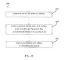
- a method of assembling a die-up array IC device packageincludes mounting an IC die to a first surface of a stiffener. The method further includes coupling a cap body to the first surface of the stiffener to form a die enclosure that substantially encloses the IC die.
- the cap bodyincludes a lid body and a frame body.
- the step of coupling the cap body to the first surface of the stiffenerincludes coupling a second surface of the frame body to the stiffener, and coupling a second surface of the lid body to a first surface of the frame body.
- the methodfurther includes encapsulating the IC die with an encapsulating material. In another embodiment, the method further includes encapsulating the IC die with an encapsulating material and forming at least one mold gate opening or at least one pressure release opening through the cap body.
- the methodfurther includes forming a central opening through the substrate, and coupling a heat slug to the second surface of the stiffener through the central opening through the substrate. Additionally or alternatively, the method further includes coupling a heat sink to the first surface of the cap body.
- FIG. 1illustrates a cross-sectional view of a conventional ball grid array (BGA) package.
- BGAball grid array
- FIGS. 2 and 3illustrate cross-sectional views of conventional BGA packages with drop-in heat spreaders.
- FIGS. 4 and 5illustrate cross-sectional views of conventional BGA packages with enhanced thermal properties.
- FIG. 6Aillustrates a cross-sectional view of a die-up BGA package, in accordance with an embodiment of the present invention, having a cap structure integrated with a stiffener.
- FIG. 6Billustrates the cap structure of FIG. 6A , in accordance with an embodiment of the present invention.
- FIGS. 7A and 7Billustrate top views of one-piece stiffener configurations having plated areas, in accordance with embodiments of the present invention.
- FIG. 7Cillustrates a top view of a two-piece stiffener configuration having a plated area, in accordance with an embodiment of the present invention.
- FIGS. 8A and 8Billustrate a cross-sectional view and bottom view, respectively, of a cap structure with protruding tab members, in accordance with an embodiment of the present invention.
- FIGS. 9A-9Cillustrate top views of a stiffener with receptacles formed in a surface, in accordance with embodiments of the present invention.
- FIG. 10illustrates a cross-sectional view of a BGA package, in accordance with an embodiment of the present invention, with a cap structure having tab members coupled with corresponding receptacles in a stiffener.
- FIG. 11illustrates a cross-sectional view of a BGA package, in accordance with an embodiment of the present invention, with mold gate openings through a cap structure, which has a surface not covered by an encapsulating material.
- FIG. 12illustrates a cross-sectional view of a BGA package, in accordance with an embodiment of the present invention, with mold gate openings through a cap structure, which is covered by an encapsulating material.
- FIG. 13illustrates a bottom view of a cap structure, in accordance with an embodiment of the present invention, with mold gate openings through a surface.
- FIG. 14illustrates a cross-sectional view of a BGA package, in accordance with an embodiment of the present invention, with an encapsulating material covering a stiffener, which has a peripheral dimension that exceeds a peripheral dimension of a cap structure.
- FIG. 15illustrates a cross-sectional view of a BGA package, in accordance with an embodiment of the present invention, with a die that is encapsulated by mold injection encapsulation.
- FIG. 16illustrates a cross-sectional view of a BGA package, in accordance with an embodiment of the present invention, with a die that is encapsulated by dam-and-fill encapsulation.
- FIG. 17illustrates a cross-sectional view of a BGA package, in accordance with an embodiment of the present invention, having a die encapsulated by mold injection encapsulation and a pressure release opening through a cap structure.
- FIG. 18illustrates a cross-sectional view of a BGA package, in accordance with an embodiment of the present invention, having a die encapsulated by dam-and-fill encapsulation and a pressure release opening through a cap structure.
- FIG. 19illustrates a cross-sectional view of a BGA package, in accordance with an embodiment of the present invention, having a cap structure with a pressure release opening.
- FIGS. 20-24illustrate cross-sectional views of BGA packages, in accordance with embodiments of the present invention, configured with enhanced thermal properties.
- FIG. 25Aillustrates a cross-sectional view of a BGA package, in accordance with an embodiment of the present invention, having a can structure integrated with a stiffener.
- FIG. 25Billustrates the can structure of FIG. 25A , in accordance with an embodiment of the present invention.
- FIG. 26illustrates a cross-sectional view of a BGA package, in accordance with an embodiment of the present invention, having ring and lid structures integrated with a stiffener.
- FIG. 27illustrates a perspective view of a ring structure with a groove formed in a surface, in accordance with an embodiment of the present invention.
- FIGS. 28-29illustrate cross-sectional views of BGA packages, in accordance with embodiments of the present invention, having lid structures recess-mounted on ring structures.
- FIGS. 30-33show flowcharts providing example steps for assembling a die-up array integrated circuit (IC) device package with enhanced thermal and electromagnetic interference (EMI) shielding properties, according to embodiments of the present invention.
- ICintegrated circuit
- EMIelectromagnetic interference
- a die-up array IC device packageincludes a plurality of electrically conductive terminals (e.g., solder balls, pins, pads, etc.) arranged in an array (e.g., columns and rows) on a bottom surface of a substrate. Signals from an IC die mounted on a top surface of the substrate are routed through the substrate to the electrically conductive terminals.
- the electrically conductive terminalsare configured to be attached to a printed circuit board (PCB).
- PCBprinted circuit board
- Examples of die-up array packagesinclude BGA (e.g., pad array carrier, pad array package, land grid array, pad grid array package), pin grid array, etc.
- a die-up array-type IC device packageincludes an IC die mounted to a first surface of a stiffener, and a package substrate coupled to a second surface of the stiffener.
- the packagefurther includes a cap structure that has a cavity formed therein. The cap structure is coupled to the first surface of the stiffener so that the stiffener and the cap structure form an enclosure, which substantially encloses the IC die.
- the die enclosureforms a thermally conductive path from the IC die to the outer surfaces of the package for enhanced heat spreading. Additionally, or in alternative embodiments, the die enclosure shields EMI emanating from the IC die, as well as EMI radiating toward the IC die from outside the package. Furthermore, in embodiments, the die enclosure can be coupled to a voltage to form an electrical potential plane (e.g., a voltage plane or a ground plane) surrounding the IC die for enhanced EMI shielding. The die enclosure also enhances rigidity and improves planarity of the printed circuit substrate, and protects the IC die from the environment (e.g., chemical corrosives, moisture, heat, vibration, and mechanical impact, etc.). Optional lock-in mechanisms on the cap structure and the stiffener (referred to herein as “protruding tabs” and “receptacles,” respectively) can further enhance the thermal, electrical, and mechanical integrity of the die enclosure.
- an electrical potential planee.g., a voltage plane or a ground plane
- the die enclosure
- the cap structurecan have various configurations. For example, described herein are a one-piece cap structure with a trapezoidal cavity and a rim, and a one-piece cap structure with a rectangular cavity and no rim (referred to herein as a “can” structure). Also described herein is a multiple-piece cap structure that has a frame-shaped portion, which is coupled to the stiffener, and a planar portion, which is coupled to the frame-shaped portion (the frame-shaped and planar portions are referred to herein as “ring” and “lid” structures, respectively). The invention is not, however, limited to these example cap structure configurations.
- cap structurecan also be referred to as “heat spreader” or a “drop-in heat spreader,” when used for thermal spreading.
- the stiffenercan be patterned in different forms (e.g., openings, cutouts, steps, etc.) or shapes (e.g., square, rectangular, circular, spoke-like, cutouts or notches and steps on one or more edges, etc.) to facilitate wire bond interconnects and to enhance package performance.
- the stiffenercan also be finished using a variety of processes, materials, and methodologies at various surfaces, spots, and locations. Openings can be formed through the stiffener to facilitate electrical interconnects between the IC die and the substrate, and the stiffener and the substrate.
- Example materials for the cap structure and the stiffenerinclude copper, aluminum, aluminum based alloys, copper based alloys, ferromagnetic materials, laminated copper/iron, other metal and combinations of metals/alloys, other thermally and electrically conductive materials (e.g., ceramics, metallized plastics, etc.), and materials described elsewhere herein.
- Conventional types of substratee.g., organic, tape, and ceramic, etc.
- advanced types of substratee.g., high density substrate, build-up substrate, Teflon substrate, etc.
- Single routing layer substrates, as well as multiple routing layer substratescan also be used.
- FIG. 1illustrates a cross-sectional view of a conventional BGA package 100 with an IC semiconductor die 115 mounted on a printed circuit substrate 110 , and a plastic molding compound 105 that encapsulates IC die 115 .
- Heat generated by IC die 115can be trapped within BGA package 100 because materials for plastic molding compound 105 and dielectric materials, such as resin epoxy or polyimide tape, for substrate 110 have low thermal conductivity.
- BGA package 100does not provide EMI shielding because materials for plastic molding compound 105 and dielectric materials, such as resin epoxy or polyimide tape, for substrate 110 are transparent to EMI.
- FIG. 2illustrates a cross-sectional view of a conventional BGA package 200 with an IC semiconductor die 215 mounted on a printed circuit substrate 210 and encapsulated by a mold compound 205 .
- BGA package 200includes a drop-in heat spreader 220 to promote dissipation of heat within plastic molding compound 205 .
- direct contact between IC die 215 and heat spreader 220is not permitted in package 200 . This is required to avoid shorting heat spreader 220 with the active surface of IC die 215 and wire bond interconnections 225 .
- heat generated by IC die 215must pass through plastic molding compound 205 in order to reach heat spreader 220 , and can therefore remain trapped within BGA package 200 .
- drop-in heat spreader 220only provides limited EMI shielding, if any.
- EMI generated outside BGA package 200can penetrate printed circuit substrate 210 and interfere with the operation of IC die 215 .
- EMI generated by IC die 215can escape through trace metal openings or gaps in printed circuit substrate 210 to outside BGA package 200 .
- FIG. 3illustrates a cross-sectional view of a conventional BGA package 300 , similar to BGA package 200 , but with a differently configured heat spreader 320 .
- BGA package 300suffers from the same thermal and electromagnetic shielding deficiencies as BGA package 200 .
- a plastic molding compound 305 and a printed circuit substrate 310trap heat generated by an IC die 315 within BGA package 300 , and EMI generated inside and outside of BGA package 300 can penetrate printed circuit substrate 310 .
- FIGS. 4 and 5illustrate cross-sectional views of further conventional BGA packages.
- FIG. 4illustrates a BGA package 400 with a metal stiffener 420 that has a larger surface area than an IC die 415 to promote heat dissipation into surrounding materials.
- Metal stiffener 420is attached to an organic substrate 410 , such as a polyimide tape or resin epoxy substrate.
- FIG. 5illustrates a cross-sectional view of a BGA package 500 , which provides a thermal and electrical connection between an IC die 515 and a printed circuit board (PCB) (not shown) through a metal heat slug 525 .
- PCBprinted circuit board
- FIG. 5illustrates a cross-sectional view of a BGA package 500 , which provides a thermal and electrical connection between an IC die 515 and a printed circuit board (PCB) (not shown) through a metal heat slug 525 .
- PCBprinted circuit board
- Metal stiffeners 420 and 520 of BGA packages 400 and 500shield EMI radiating toward IC dies 415 and 515 from the area underneath the IC dies.
- BGA packages 400 and 500do not shield EMI radiating towards IC dies 415 and 515 from the area above the active surface of the IC dies.
- BGA packages 400 and 500also do not prevent EMI emanating from IC dies 415 and 515 from escaping the package through the area above the active surface of the IC dies.
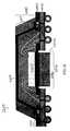
- FIG. 6Aillustrates a cross-sectional view of a die-up BGA package 600 , in accordance with an embodiment of the present invention.
- BGA package 600provides for enhanced heat spreading and EMI shielding.
- BGA package 600includes a printed circuit substrate 610 , a stiffener 620 , and a cap body 625 .
- An IC die 615is mounted to a center region of a first surface 621 of stiffener 620 with a die attach material 624 , such as an epoxy or solder.
- Cap body 625is coupled to first surface 621 of stiffener 620 , forming a die enclosure 680 that substantially surrounds IC die 615 .
- a second surface 622 of stiffener 620is attached to a first surface 611 of substrate 610 .
- a plurality of solder balls 613is coupled to a second surface 612 of substrate 610 . Solder balls 613 are reflowed to attach package 600 to a PCB
- BGA package 600further includes openings 635 , wire bonds 640 , 650 , and 655 , and mold compound 605 .
- Openings 635 formed in stiffener 620facilitate interconnection of one or more wire bonds 640 between corresponding pads 645 on IC die 615 and substrate 610 .
- Pads 645can be any type of signal pads of IC die 615 , including I/O pads, voltage pads, ground pads, etc.
- Openings 635also facilitate interconnection of one or more wire bonds 655 between stiffener 620 and substrate 610 (e.g., traces, contacts, ground rings, ground planes, voltage planes, etc. of substrate 610 ).
- One or more wire bonds 650couple corresponding pads 646 on IC die 615 to stiffener 620 .
- Pads 646can be any type of signal pads of IC die 615 , such as I/O pads, voltage pads, ground pads, etc.
- a mold compound 605encapsulates IC die 615 and wire bonds 640 , 650 , and 655 .
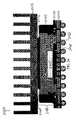
- FIG. 6Billustrates a cross-sectional view of cap body 625 , shown in FIG. 6A , in accordance with an embodiment of the present invention.
- cap body 625has a planar top portion 660 , planar sidewall portions 685 , and a rim 665 extending around a bottom periphery of cap body 625 .
- Sidewall portions 685couple top portion 660 to rim 665 , and are angled outward from top portion 660 .
- top portion 660 and sidewall surfaces 685are shown as planar but can also be non-planar (e.g., curved, or other shapes).
- Cap body 625further has a first surface 690 and a second surface 691 .
- a portion of first surface 690is exposed through mold compound 605 , as shown in FIG. 6A .
- Second surface 691has cavity 630 formed therein. Cavity 630 is shown in FIG. 6B as having a trapezoidal shaped cross-section, but can have other shapes, including rectangular, etc.
- Second surface 691 of cap body 625(at rim 665 ) is coupled to stiffener 620 , as shown in FIG. 6A .
- Example materials for substrate 610include organic (e.g., BT, FR4, etc.), ceramic, glass, tape, and other materials.
- Substrate 610can have one or more electrical routing layers, which are constructed through lamination, build-up, or other processes.
- Example materials for stiffener 620 and cap body 625include copper, aluminum, aluminum based alloys, copper based alloys, ferromagnetic materials, laminated copper/iron, other metals and combinations of metals/alloys, other thermally and electrically conductive materials (e.g., ceramics, metallized plastics, etc.), and other materials described elsewhere herein.
- Stiffener 620 and cap body 625can be made of the same material or different materials.
- Stiffener 620can have any thickness, depending on the particular application. For example, in embodiments, stiffener 620 can have a thickness anywhere in the range of 0.01 mm to 10 mm.
- stiffener 620can have a thickness in the range of about 0.1 mm to about 0.5 mm. In another example embodiment, stiffener 620 can have a thickness of about 1.17 mm.
- cap body 625can have any thickness, depending on the particular application. For example, in embodiments, cap body 625 can have a thickness anywhere in the range of 0.01 mm to 10 mm. In an example embodiment, cap body can have a thickness in the range of about 0.1 mm to about 1.0 mm.
- surfaces of stiffener 620can be finished or un-finished.
- surfaces of stiffener 620can be finished using processes such as micro-etch or oxidation to promote adhesion with mold compound 605 .
- first surface 621 of stiffener 620can be patterned (e.g. spot, strip, bar, ring, other shapes) with one or more electrically conductive plated areas (e.g., silver, solder, nickel, gold, metal combinations/alloys, etc.) for enhanced coupling of wire bonds 650 to first surface 621 .
- Stiffener 620can also be patterned in various forms to improve package mechanical, thermal, and electrical performances and package reliability. (See, e.g. U.S. patent application Ser. No.
- die enclosure 680When stiffener 620 and cap body 625 are coupled together, as shown in FIG. 6A , die enclosure 680 is formed. Die enclosure 680 shields EMI emanating from IC die 615 , as well as EMI radiating toward IC die 615 from outside package 600 . In order to provide enhanced EMI protection, die enclosure 680 can be coupled to a ground potential (e.g., to create a Faraday cage), or to other electrical potentials (i.e., to create a voltage plane). When stiffener 620 is coupled with ground pads 646 (or bond pads of other electrical potentials) on IC die 615 , die enclosure 680 operates as a ground potential (or other electrical potential) plane for IC die 615 . Furthermore, this ground potential plane can be externally accessed at first surface 690 of top portion 660 of cap body 625 , if desired.
- a ground potentiale.g., to create a Faraday cage
- other electrical potentialsi.e., to create a voltage plane
- electrically conductive adhesivessuch as epoxy filled with silver particles or flakes, can be used to couple cap body 625 to stiffener 620 .
- Soldering materialssuch as tin-lead or silver, can also be used to couple cap body 625 to stiffener 620 through processes such as solder plating and reflow or screen printing of paste and reflow.
- thermally conductive adhesivescan be used to enhance thermal contact between cap body 625 and stiffener 620 .
- FIGS. 7A-7Cshow example configurations for stiffener 620 , according to embodiments of the present invention.
- Thermally and/or electrically conductive materialse.g., silver, solder, nickel, gold, metal combinations/alloys, etc.
- FIG. 7Aillustrates a top view of a one-piece stiffener 702 with a plurality of wire bond openings 705 and a plated ring-shaped area 710 .
- wire bond openings 705can be trapezoidal shaped, although openings 705 can have other shapes, including rectangular, oval, etc.
- Ring area 710is plated with an electrically conductive material to enhance electrical contact with cap body 625 .
- FIG. 7Billustrates a top view of a one-piece stiffener 704 with a trapezoidal wire bond opening 705 , multiple cutouts 725 , and plated areas 730 , 735 , and 740 .
- Cutouts 725are recessed edge portions of stiffener 620 . Cutouts 725 can be used to allow wire bond connections between an IC die and a package substrate in the areas of cutouts 725 .
- Areas 730 , 735 , and 740are plated with an electrically conductive material. Area 730 has an elongated strip shape, area 735 is circular, and area 740 is rectangular. Note that plated areas can have alternative shapes and/or sizes. Areas 730 , 735 , and 740 can be used to enhance electrical contact with cap body 625 .
- FIG. 7Cillustrates a top view of a two-piece stiffener 706 , with a first stiffener portion 765 separated by a channel 755 from a second stiffener portion 760 .
- Two-piece stiffener 706 of FIG. 7Cincludes wire bond openings 750 , 751 , and 752 , through first stiffener portion 765 .
- a plated U-shaped area 770is patterned on first stiffener portion 765 .
- wire bond openings 750 , 751 , and 752can be rectangular shaped, although, openings 750 , 751 , and 752 can have other shapes (e.g., trapezoidal, etc.).
- U-shaped area 770is plated with an electrically conductive material to enhance electrical contact with cap body 625 .
- second stiffener portion 760is electrically isolated from first stiffener portion 765 by channel 755 .
- second stiffener portion 760is also electrically isolated from cap body 625 (when attached to stiffener 620 ) because cap body 625 is not electrically coupled to second stiffener portion 760 .
- a non-electrically conductive adhesivemay couple second stiffener portion 760 and cap body 625 .
- second stiffener portion 760can be coupled to a different potential from first stiffener portion 765 , if desired.
- the inventionis not, however, limited to the example stiffener configurations shown in FIGS. 7A-7C .
- the inventioncan be implemented with other stiffener configurations having differently shaped wire bond openings/cutouts (e.g., circular openings, rectangular cutouts, etc.), differently shaped electrically conductive plated areas (e.g., circular ring-shaped area, or other shapes), and different quantities of wire bond openings/cutouts and electrically conductive plated areas.
- FIGS. 8A and 8Billustrate an example configuration of a cap body 805 , in accordance with an embodiment of the present invention. Cap body 805 is configured to enhance structural interlocking with a stiffener.
- FIG. 8Aillustrates a cross-sectional view of cap body 805 having a rim 810 .
- FIG. 8Billustrates a bottom view of cap body 805 .
- the bottom surface of rim 810is patterned with one or more protruding tab members (e.g., through stamping or other metal forming process).
- protruding tab memberse.g., through stamping or other metal forming process.
- FIGS. 8A and 8Bare frustum-shaped tab 815 , conical-shaped tabs 820 , conical-shaped tab 825 , and oblong-shaped tab 830 .
- the inventionis not, however, limited to the example tab quantities, shapes, and sizes shown in FIGS. 8A and 8B .
- a cap bodycan have more or fewer numbers of tabs patterned on the bottom surface, the tabs can have the same shape or different shapes (e.g., conical, frustum, oblong, or other shapes), and the tabs can have the same size or different sizes (e.g., diameter, height, depth, etc.).
- shape or different shapese.g., conical, frustum, oblong, or other shapes
- the tabscan have the same size or different sizes (e.g., diameter, height, depth, etc.).
- a cap body(such as cap body 625 or 805 ) can have various shapes.
- cap body 805can be round.
- a cap bodycan have other shapes, including rectangular (e.g., square), elliptical, oval, or any other shape.
- FIGS. 9A-9Cshow example stiffener configurations, according to embodiments of the present invention.
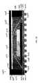
- FIG. 9Aillustrates a top view of a stiffener 950 with a plurality of wire bond openings 912 and a plurality of receptacles 902 , 904 , 906 , 908 , and 910 formed in the top surface.
- Receptacles 902 and 904are circular-shaped indentations, and indentation 902 has a larger diameter than indentation 904 .
- Receptacle 906is a circular-shaped opening
- receptacle 908is a rectangular-shaped opening.
- Receptacle 910is a rectangular-shaped edge (e.g., corner) cutout.
- Receptacles 902 , 904 , 906 , 908 , and 910are configured to be coupled with corresponding tabs patterned on the bottom surface of a cap body to strengthen structural coupling of the cap body to the stiffener.
- receptacles 902may have conical cross-sections, etc.
- FIG. 9Billustrates a top view of a stiffener 960 with a wire bond opening 928 , a plurality of wire bond cutouts 930 , and receptacles 920 , 922 , 924 , and 926 formed in the top surface.
- Receptacles 920are circular-shaped openings
- receptacle 922is a circular-shaped opening with a larger diameter than receptacles 920
- receptacle 924is a rectangular-shaped opening.
- Receptacle 926is a rectangular-shaped edge (e.g., corner) cutout.
- Receptacles 920 , 922 , 924 , and 926are configured to be coupled with corresponding tabs patterned on the bottom surface of a cap body to strengthen structural coupling of the cap body to the stiffener.
- FIG. 9Cillustrates a top view of a stiffener 970 with a plurality of wire bond cutouts 938 , and receptacles 930 , 932 , 934 , and 936 formed in the top surface.
- Receptacles 930are circular-shaped openings
- receptacle 932is a circular-shaped opening with a larger diameter than receptacles 930
- receptacle 934is a rectangular-shaped opening.
- Receptacle 936is a rectangular-shaped edge (e.g., corner) cutout.
- Receptacles 930 , 932 , 934 , and 936are configured to be coupled with corresponding tabs patterned on the bottom surface of a cap body to strengthen structural coupling of the cap body to the stiffener.
- the receptacle configurations shown in the example stiffeners of FIGS. 9A-9Cfacilitate structural coupling of a cap body to the stiffener in a particular orientation.
- the inventionis not, however, limited to the example receptacle quantities, locations, types, shapes, and sizes shown in FIGS. 9A-9C .
- a stiffenercan have more or fewer numbers of receptacles formed in the top surface, and in the same or in different locations than the example configurations shown in FIGS. 9A-9C .
- the receptaclescan be of the same type or of different types (e.g., opening, indentation, cutout, etc.), can have the same shape or different shapes (e.g., circular, rectangular, or other shapes), and can have the same size or different sizes (e.g., diameter, width, depth, etc.).
- opening, indentation, cutout, etc.can have the same shape or different shapes (e.g., circular, rectangular, or other shapes), and can have the same size or different sizes (e.g., diameter, width, depth, etc.).
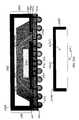
- FIG. 10illustrates a cross-sectional view of a BGA package 1000 , in accordance with an example embodiment of the present invention.
- FIG. 10shows receptacles 1070 , 1074 , and 1078 formed in a stiffener 1020 .
- Receptacles 1070 , 1074 , and 1078are configured to be coupled with corresponding tabs 1072 , 1076 , and 1080 , respectively, patterned on a rim 1065 of a cap body 1025 . This coupling helps to ensure tight lock-in of cap body 1025 with stiffener 1020 .
- electrically and/or thermally conductive adhesivescan be deposited at receptacles 1070 , 1074 , and 1078 prior to attaching cap body 1025 to stiffener 1020 .
- electrically and/or thermally conductive adhesivese.g., silver filled epoxy
- Integrating an encapsulating material, such as glob top or plastic molding compound, with the die enclosurecan enhance the structural rigidity of the BGA package and enhance the planarity of the package substrate.
- the combination of the encapsulating material and the die enclosurecan reduce IC die cracking, delamination and substrate warpage. Integrating the encapsulating material with the die enclosure also enhances environmental protection. For example, they can provide protection against mechanical stress, impact, vibration, chemical corrosives, moistures, heat exposure, radiation, etc.
- attaching the IC die directly to the die enclosureadds mass to the die support and helps reduce microphonics caused by shock or vibrations
- IC die encapsulation processescan be used to integrate the encapsulating material with the die enclosure.
- encapsulation techniquessuch as dam-and-fill (glob top), injection molding, strip or panel over-molding, saw-singulation, and any other IC die encapsulation processes can be used.
- Typical encapsulating materialssuch as plastic molding compound, have low thermal conductivity (e.g., about 0.2 to 0.9 W/mK) and therefore create a bottleneck for heat spreading in conventional die-up array packages.
- the die enclosureeliminates this bottleneck because it provides a thermally conductive path from the bottom surface of the IC die to the outer surfaces of the package.
- Example materials for die enclosuresinclude copper, aluminum, aluminum based alloys, copper based alloys, ferromagnetic materials, laminated copper/iron, other metals and combinations of metals/alloys, other thermally and electrically conductive materials (e.g., ceramics, metallized plastics, etc.), and other materials described elsewhere herein.
- materials for the die enclosurehave high thermal conductivity (e.g., approximately 390 W/mK for copper) and therefore promote heat spreading.
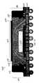
- FIG. 11illustrates a cross-sectional view of a BGA package 1100 , in accordance with an embodiment of the present invention.
- Package 1100includes a cap structure having one or more mold gate openings and a surface that is exposed through an encapsulating material.
- cap body 625has two mold gate openings 1105 through slanted sidewall portions 685 .
- Mold gate openings 1105enable mold compound 605 to flow or be injected into cavity 630 .
- First surface 690 of top portion 660 of cap body 625is exposed through mold compound 605 (e.g., not covered).
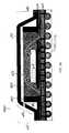
- FIG. 12illustrates a cross-sectional view of a BGA package 1200 , in accordance with an embodiment of the present invention.
- Package 1200has a cap structure with one or more mold gate openings.
- cap body 625has two mold gate openings 1205 through slanted sidewall portions 685 .
- Mold gate openings 1205enable mold compound 605 to flow or be injected into cavity 630 .
- first surface 690 of cap body 625is entirely covered by mold compound 605 .
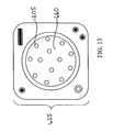
- FIG. 13illustrates a bottom view of cap body 625 , in accordance with an embodiment of the present invention.
- cap body 625has a plurality of circular mold gate openings 1305 through top portion 660 .
- mold gate openings 1305enable flow of mold compound 605 into the area of cavity 630 , above the active surface of IC die 615 , without requiring higher pressure because they are located above the active surface of IC die 615 .
- a diameter of mold gate openingsshould be selected to limit passage of EMI; however, the smaller the diameter, the higher the pressure required for injection molding.
- Mold gate opening diametercan be, for example, in the range of about 0.5 mm to about 3 mm (e.g., a diameter of about 1.5 mm can shield EMI having highest harmonic frequencies of up to 10 GHz), and can also be outside of this range depending on the particular application.
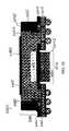
- FIG. 14illustrates a cross-sectional view of a BGA package 1400 , in accordance with an embodiment of the present invention.
- mold compound 605covers stiffener 620
- a peripheral dimension 1405 of stiffener 620exceeds a peripheral dimension 1410 of cap body 625 .
- Peripheral dimension 1405 of stiffener 620can exceed (as shown in FIG. 14 ), be equal to (as shown in FIGS. 17 and 18 , described below), or be less than (not shown) peripheral dimension 1410 of cap body 625 .
- FIG. 15illustrates a cross-sectional view of a BGA package 1500 , in accordance with an embodiment of the present invention.
- cap body 625is attached to stiffener 620 before encapsulating IC die 615 .
- Mold gate openings 1505 through sidewall portions 685 of cap body 625facilitate injection of mold compound 605 into cavity 630 .
- FIG. 16illustrates a cross-sectional view of a BGA package 1600 , in accordance with an embodiment of the present invention.
- a dam 1610is applied to stiffener 620 and/or rim 665 around the periphery of cap body 625 .
- Mold compound 605is deposited bewteen dam 1610 and cap body 625 , and flows into cavity 630 through mold gate openings 1605 .
- first surface 690 of top portion 660 of cap body 625is exposed through mold compound 605 (e.g., not covered).
- FIG. 17illustrates a cross-sectional view of a BGA package 1700 , in accordance with an embodiment of the present invention.
- cap body 625is attached to stiffener 620 after encapsulating IC die 615 (such as by a mold injection encapsulation process).
- an air gap 1720exists between cap body 625 and mold compound 605 in cavity 630 .
- Pressure within cavity 630 due to air gap 1720can build up at elevated temperatures during assembly, qualification, and testing of BGA package 1700 .
- a pressure release opening 1715 through sidewall portion 685 of cap body 625allows gas, which is released from the materials within cavity 630 , to escape from air gap 1720 and balance cavity pressure with the ambient pressure.
- FIG. 18illustrates a cross-sectional view of a BGA package 1800 , in accordance with an embodiment of the present invention.
- mold compound 605is deposited within a dam 1810 , around IC die 615 , using a dam-and-fill encapsulation process.
- cap body 625is attached to stiffener 620 .
- an air gap 1820exists between cap body 625 and mold compound 605 in cavity 630 .
- a pressure release opening 1815 through sidewall portion 685 of cap body 625allows gas, which is released from the materials within cavity 630 , to escape from air gap 1820 and balance cavity pressure with the ambient pressure.
- FIG. 19illustrates a cross-sectional view of a BGA package 1900 , in accordance with an embodiment of the present invention.
- a pressure release opening 1915is formed through top portion 660 of cap body 625 .
- a diameter of pressure release opening 1915is selected to limit passage of EMI.
- the diameter of pressure release opening 1915can be, for example, in the range of about 0.2 mm to about 2 mm (e.g., a diameter of about 0.5 mm can shield EMI having highest harmonic frequencies of up to 30 GHz), and can also be outside of this range, depending on the particular application.
- the diameterneed not meet mold gate opening diameter requirements, described above, because cap structure 625 is attached to stiffener 620 after encapsulation. Therefore, mold compound 605 need not flow through pressure release opening 1915 into cavity 630 .
- FIGS. 20-24illustrate cross-sectional views of BGA packages, in accordance with embodiments of the present invention, with additional thermal enhancements. These additional thermal enhancements can also be incorporated into the BGA packages described elsewhere herein, including those shown in FIGS. 12 , 17 - 19 , 25 , 26 , 28 and 29 .
- FIG. 20illustrates a cross-sectional view of a BGA package 2000 , in accordance with an embodiment of the present invention.
- BGA package 2000includes and IC die 2015 , a package substrate 2010 , a stiffener 2020 , a cap body 2025 , and a thermal/electrical connector 2040 .
- IC die 2015is mounted to a central area of top surface 2001 of stiffener 2020 .
- a second surface 2002 of stiffener 2020is attached to substrate 2010 .
- Substrate 2010has a central opening 2070 that exposes a central area 2006 of second surface 2002 of stiffener 2020 .
- Cap body 2025is attached to top surface 2001 of stiffener 2020 , forming a die enclosure 2080 .
- Thermal/electrical connector 2040(also referred to herein as a “heat slug”) is attached to central area 2006 of second surface 2002 of stiffener 2020 through opening 2070 in substrate 2010 .
- Thermal/electrical connector 2040is configured to be soldered to a PCB during surface mount.
- BGA package 2000provides enhanced heat spreading because thermal/electrical connector 2040 reduces the thermal resistance between IC die 2015 and the PCB.
- connector 2040can be attached to a ground or other potential of the PCB.
- BGA package 2000also provides enhanced EMI shielding because thermal/electrical connector 2040 reduces the ground (or other voltage) connection impedance of die enclosure 2080 to the PCB.
- BGA package 2000is encapsulated by dam-and-fill encapsulation. After cap body 2025 is attached to stiffener 2020 , a dam 2045 is applied around the periphery of cap body 2025 , partially covering stiffener 2020 . A mold compound 2005 is subsequently applied, filling the area between dam 2045 and cap body 2025 . Mold compound 2005 flows into a cavity 2030 through one or more mold gate openings 2050 in sidewall portions 2085 of cap body 2025 .
- FIG. 21illustrates a cross-sectional view of a BGA package 2100 , in accordance with an embodiment of the present invention.
- BGA package 2100is similar to BGA package 2000 , shown in FIG. 20 , except that the edges of stiffener 2020 are not flush with the edges of substrate 2010 . Instead, the edges of stiffener 2020 are flush with those of cap body 2025 .
- FIG. 22illustrates a cross-sectional view of a BGA package 2200 , in accordance with an embodiment of the present invention.
- BGA package 2200is similar to BGA package 2000 , shown in FIG. 20 , except that BGA package 2200 is encapsulated by a mold injection process.
- mold compound 2005does not extend to the edges of stiffener 2020 , leaving areas 2201 of stiffener 2020 exposed through, or not covered by mold compound 2005 .
- FIG. 23illustrates a cross-sectional view of a BGA package 2300 , in accordance with an embodiment of the present invention.
- BGA package 2300is similar to BGA package 2200 , shown in FIG. 22 , except that mold compound 2005 extends to the edges of stiffener 2020 .
- BGA package 2300can be encapsulated over the entire substrate strip or panel and separated by a saw singulation process.
- FIG. 24illustrates a cross-sectional view of a BGA package 2400 , in accordance with an embodiment of the present invention.
- BGA package 2400is similar to BGA package 1600 , shown in FIG. 16 , except that an external heat sink 2475 is attached to top portion 2460 of cap body 2425 with a thermally and/or electrically conductive interface or adhesive material 2470 .
- Cap body 2425 and a stiffener 2420form a die enclosure 2480 .
- External heat sink 2475enhances heat spreading; however, it can operate as an antenna that undesirably radiates EMI.
- a heat sink ground jumper wirecan be used to ground the external heat sink to a PCB.
- a ground jumper wireis not required, however, if the external heat sink is attached to a grounded die enclosure.
- a heat sink ground jumper wireis not required for BGA package 2400 because external heat sink 2475 is attached to die enclosure 2480 , which is coupled to a ground potential through ground wires bonds 2430 and/or 2435 .
- a cap structure in a die-up array-type IC device packagecan have various configurations.
- Another example configurationis a one-piece cap structure having no rim, which is referred to herein as a “can” structure.
- An example of a can structureis described as follows with respect to FIG. 25 .
- FIG. 25Aillustrates a cross-sectional view of a BGA package 2500 , in accordance with an embodiment of the present invention.
- BGA package 2500includes an IC die 2515 , a printed circuit substrate 2510 , a stiffener 2520 , and a can body 2525 .
- IC die 2515is mounted to a center region of a first surface 2521 of stiffener 2520 with a die attach material 2524 , such as epoxy or solder.
- Can body 2525 and stiffener 2520form a die enclosure 2580 that substantially surrounds IC die 2515 .
- a second surface 2522 of stiffener 2520is attached to a first surface 2511 of a package substrate 2510 .
- a plurality of solder balls 2513is coupled to a second surface 2512 of substrate 2510 . Solder balls 2513 are reflowed to attach package 2500 to a PCB.
- BGA package 2500further includes openings 2535 , wire bonds 2540 and 2550 , and a mold compound 2505 .
- Openings 2535 formed in stiffener 2520facilitate interconnection of one or more wire bonds 2540 between corresponding bond pads 2545 and substrate 2510 .
- Pads 2545can be any type of signal pads of IC die 2515 , such as I/O pads, voltage pads, ground pads, etc.
- One or more wire bonds 2550couple ground pads 2546 to stiffener 2520 .
- Pads 2546can be any type of signals pads of IC die 2515 , such as I/O pads, voltage pads, etc.
- Mold compound 2505encapsulates IC die 2515 and wire bonds 2540 and 2550 .
- FIG. 25Billustrates a cross-sectional view of can body 2525 , shown in FIG. 25A .
- a can body 2525has a horizontal planar top portion 2560 and sidewall portions 2585 that form a ninety degree angle to top portion 2560 .
- Can body 2525further has a first surface 2590 and a second surface 2591 .
- Second surface 2591has a cavity 2530 with a rectangular cross-section formed therein. Second surface 2591 is coupled to a first surface 2521 of stiffener 2520 .
- Die enclosure 2580provides enhanced heat spreading and EMI shielding, while also providing enhanced structural integrity and environmental protection for package 2500 .
- BGA package 2500is similar to BGA package 600 , described above. Accordingly, features of BGA package 600 described above are generally similar to the corresponding features of BGA package 2500 (e.g., example materials for the can structure, stiffener, substrate, encapsulating material, etc.; use of electrically conductive plated areas to enhance electrical coupling of the can structure to the stiffener; use of interlocking tabs and receptacles to enhance structural coupling of the can structure to the stiffener; use of a thermal/electrical connector and/or an external heart sink to enhance heat spreading; etc.).
- these featuresare not necessarily described in detail here for reasons of brevity.
- a cap structureis a two-piece cap structure.
- a two-piece cap structuremay have a frame-shaped bottom portion, which is coupled to a stiffener, and a planar top portion, which is coupled to the frame-shaped portion.
- the frame-shaped bottom and planar top portionsare referred to herein as “ring” and “lid” structures, respectively, and are described as follows with respect to FIGS. 26-29 .
- FIG. 26illustrates a cross-sectional view of a BGA package 2600 , in accordance with an embodiment of the present invention.
- BGA package 2600includes an IC die 2615 , a printed circuit substrate 2610 , a stiffener 2620 , a ring structure 2625 , and a lid structure 2626 .
- ring structure 2625is a frame-shaped structure having a central opening.
- Lid structure 2626is planar and has first and second surfaces 2661 and 2662 , respectively.
- a peripheral portion of second surface 2662 of lid structure 2626is coupled to a first surface 2624 of ring structure 2625 .
- ring structure 2625 and lid structure 2626form a cavity 2630 .
- Cavity 2630has a rectangular cross-section.
- a second surface 2623 of ring structure 2625is attached to a first surface 2621 of stiffener 2620 .
- IC die 2615is mounted to a center region of first surface 2621 of stiffener 2620 with a die attach material 2675 , such as epoxy or solder.
- a die attach material 2675such as epoxy or solder.
- Lid structure 2626 , ring structure 2625 , and stiffener 2620form a die enclosure 2680 that substantially surrounds IC die 2615 .
- a second surface 2622 of stiffener 2620is attached to a first surface 2611 of package substrate 2610 .
- a plurality of solder balls 2613is coupled to a second surface 2612 of substrate 2610 . Solder balls 2613 are reflowed to attach package 2600 to a PCB.
- BGA package 2600further includes openings 2635 , wire bonds 2640 and 2650 , and mold compound 2605 . Openings 2635 formed in stiffener 2620 facilitate interconnection of one or more wire bonds 2640 between corresponding bond pads 2645 and substrate 2610 . One or more wire bonds 2650 couple ground pads 2646 to stiffener 2620 . Pads 2645 and 2646 can be any type of signal pads of IC die 2615 , such as I/O pads, voltage pads, ground pads, etc. Mold compound 2605 encapsulates IC die 2615 and wire bonds 2640 and 2650 . Dam-and-fill encapsulation, or any other encapsulation techniques, can be used to encapsulate IC die 2615 before attaching lid 2626 .
- Mold compound 2605can be filled to just below first surface 2624 of ring structure 2625 so that a gap 2670 is formed between second surface 2662 of lid structure 2626 and mold compound 2605 .
- die enclosure 2680can be completely filled with mold compound 2605 , so that no gap remains.
- BGA package 2600further includes a pressure release opening 2665 that extends through a sidewall portion of ring structure 2625 .
- FIG. 27illustrates a perspective view of ring structure 2625 , which has a groove 2710 formed on first surface 2624 .
- groove 2710forms pressure release opening 2665 .
- Gaswhich can be released from materials within cavity 2630 , can escape through pressure release opening 2665 and balance the cavity pressure with the ambient pressure.
- ring structure 2625can have a pressure release opening formed through an edge portion (not shown).
- FIG. 28illustrates a cross-sectional view of a BGA package 2800 , in accordance with an embodiment of the present invention, with ring and lid structures integrated with a stiffener.
- BGA package 2800is similar to BGA package 2600 , shown in FIG. 26 , except that a peripheral dimension 2801 of lid structure 2626 is within a peripheral dimension 2802 of ring structure 2625 .
- lid structure 2626can be “recess-mounted” to ring structure 2625 , as shown in FIG. 28 .
- lid structure 2626resides in a recessed inner edge 2804 located around the top surface of ring structure 2625 .
- first surface 2661 of lid structure 2626can be substantially planar with first surface 2624 of ring structure 2625 . Recess-mounting lid structure 2626 on ring structure 2625 , as shown in FIG. 28 , may enhance structural interlocking of lid structure 2626 and ring structure 2625 .
- FIG. 29illustrates a cross-sectional view of a BGA package 2900 , in accordance with an embodiment of the present invention, with ring and lid structures integrated with a stiffener.
- BGA package 2900is similar to BGA package 2800 , shown in FIG. 28 , except when lid structure 2626 is recess-mounted on ring structure 2625 , first surface 2661 of lid structure 2626 protrudes above first surface 2624 of ring structure 2625 .
- a recessed inner edge 2902 around the top of ring structure 2625has a depth that is less than a thickness of lid structure 2626 .
- Recess-mounting lid structure 2626 on ring structure 2625may enhance structural interlocking of lid structure 2626 and ring structure 2625 .
- Die enclosure 2680shown in FIGS. 26, 28 , and 29 , provides enhanced heat spreading and EMI shielding, while also providing enhanced structural integrity and environmental protection for packages 2600 , 2800 , and 2900 , respectively.
- BGA packages 2600 , 2800 , and 2900are similar to BGA package 600 , described above.
- features of BGA package 600 described aboveare generally similar to the corresponding features of BGA packages 2600 , 2800 , and 2900 (e.g., example materials for ring and lid structures, stiffener, substrate, encapsulating material, etc.; use of electrically conductive plated areas to enhance electrical coupling of the ring structure to the stiffener; use of interlocking tabs and receptacles to enhance structural coupling of the ring structure to the stiffener; use of a thermal/electrical connector and/or an external heart sink to enhance heat spreading; etc.).
- these featuresare not necessarily described in detail here for reasons of brevity.
- FIG. 30shows a flowchart 3000 providing steps for assembling a die-up array IC device package with enhanced thermal and/or EMI shielding properties according to one or more embodiments of the present invention.
- FIGS. 31-33provide additional optional steps, according to further embodiments of the present invention. The steps of FIGS. 30-33 do not necessarily have to occur in the order shown, as will be apparent to persons skilled in the relevant art(s) based on the teachings herein. Other operational and structural embodiments will be apparent to persons skilled in the relevant art(s) based on the following discussion. These steps are described in detail below.
- Flowchart 3000is shown in FIG. 30 , and begins with step 3005 .
- an IC dieis mounted to a first surface of a stiffener.
- the IC dieis IC die 615 and the stiffener is stiffener 620 , as shown in FIG. 6A , or any one of the stiffeners shown in FIGS. 7A-7C , 9 A- 9 C, 10 - 12 , 14 - 26 , 28 , and 29 .
- a cap bodyis coupled to the first surface of the stiffener.
- the first surface of the stiffener and a cavity in a second surface of the cap bodyform an enclosure that substantially encloses the IC die.
- the cap bodyis cap body 625
- the stiffeneris stiffener 620
- the cavityis cavity 630
- the IC dieis IC die 615
- the die enclosureis die enclosure 680 , as shown in FIG. 6A , or any one of the corresponding elements shown in FIGS. 6 B, 7 A-C, 8 A and 8 B, 9 A- 9 C, 10 - 26 , 28 , and 29 .
- a second surface of the stiffeneris coupled to a first surface of a substrate.
- the stiffeneris stiffener 620 and the substrate is substrate 610 , shown in FIG. 6A , or any of the substrates shown in FIGS. 10-12 , 14 - 26 , 28 , and 29 .
- step 3010 of flowchart 3000includes the additional steps shown in FIG. 31 .
- a second surface of a frame bodyis coupled to the first surface of the stiffener.
- the frame bodyis ring structure 2625
- the stiffeneris stiffener 2610 , as shown in FIG. 26 , or any of the ring structures shown in FIGS. 27-29 .
- a second surface of a lid bodyis coupled to a first surface of the frame body.
- the stiffener, the frame body, and the lid bodyform an enclosure that substantially encloses the IC die.
- the lid bodyis lid structure 2626
- the frame bodyis ring structure 2625
- the stiffeneris stiffener 2620
- the die enclosureis die enclosure 2680
- the IC dieis IC die 2615 , as shown in FIG. 26 , or any of the corresponding elements shown in FIGS. 28 and 29 .
- flowchart 3000includes one or more of the additional steps shown in FIG. 32 .
- steps 3205 , 3210 , and 3215can be performed.
- step 3205at least one mold gate opening is formed through a portion of the cap body.
- the cap bodyis cap body 625
- the at least one mold gate openingis mold gate opening 1105 , as shown in FIG. 11 , or any of the mold gate openings shown in FIGS. 12, 13 , 15 , 16 , 20 , 21 , and 24 .
- step 3210at least one pressure release opening is formed through a portion of the cap body.
- the cap bodyis cap body 625
- the at least one pressure release openingis pressure release opening 1715 , as shown in FIG. 17 , or any of the pressure release openings shown in FIGS. 18 and 19 .
- the IC dieis encapsulated with an encapsulating material.
- the IC dieis IC die 615
- the encapsulating materialis mold compound 605 , as shown in FIG. 6A , or any one of the corresponding elements shown in FIGS. 10-12 , 14 - 26 , 28 , and 29 .
- conventional IC die encapsulation processescan be used, such as dam-and-fill (glob top), injection molding, strip or panel over-molding, saw-singulation, and any other IC die encapsulation processes.
- flowchart 3000includes one or more of the additional steps pertaining to thermal enhancement shown in FIG. 33 .
- steps 3305 and 3310need not be performed in conjunction with step 3315
- step 3315need not be performed in conjunction with steps 3305 and 3310 .
- a central openingis formed through the substrate.
- the substrateis substrate 2010
- the central openingis opening 2070 , as shown in FIG. 20 , or any of the corresponding elements shown in FIGS. 21-23 .
- a heat slug(also referred to herein as a “thermal/electrical connector”) is coupled to a portion of the second surface of the stiffener that is exposed through the central opening through the substrate.
- the heat slugis thermal/electrical connector 2040
- the stiffeneris stiffener 2020
- the exposed second surface of the stiffeneris exposed central area 2006
- the substrateis substrate 2010
- the central opening through the substrateis opening 2070 , as shown in FIG. 20 , or any of the corresponding elements shown in FIGS. 21-23 .
- an external heat sinkis coupled to a portion of the cap body.
- the external heat sinkis external heat sink 2475
- the cap bodyis cap body 2425
- the portion of the cap body to which the external heat sink is attachedis top portion 2460 , as shown in FIG. 24 .
Landscapes
- Engineering & Computer Science (AREA)
- Microelectronics & Electronic Packaging (AREA)
- Power Engineering (AREA)
- Computer Hardware Design (AREA)
- Physics & Mathematics (AREA)
- General Physics & Mathematics (AREA)
- Condensed Matter Physics & Semiconductors (AREA)
- Chemical & Material Sciences (AREA)
- Health & Medical Sciences (AREA)
- Electromagnetism (AREA)
- Toxicology (AREA)
- Materials Engineering (AREA)
- Dispersion Chemistry (AREA)
- Cooling Or The Like Of Semiconductors Or Solid State Devices (AREA)
Abstract
Description
- The following patent application of common assignee is related to the present application, and is herein incorporated by reference in its entirety: “Ball Grid Array Package Enhanced With A Thermal And Electrical Connector,” U.S. patent application Ser. No. 10/284,312, filed Oct. 31, 2002.
- The following application of common assignee is related to the present application, has the same filing date as the present application, and is herein incorporated by reference in its entirety: “Multipiece Apparatus For Thermal And Electromagnetic Interference (EMI) Shielding Enhancement In Die-Up Array Packages And Method Of Making The Same,” Atty. Dkt. No. 1875.5480001, Ser. No. ______.
- 1. Field of the Invention
- The invention relates generally to the field of integrated circuit (IC) device packaging technology and, more particularly to thermal enhancement and electromagnetic interference (EMI) shielding in IC device packages.
- 2. Background Art
- IC semiconductor dies are typically mounted in or on a package that is attached to a printed circuit board (PCB). Example IC device packages include ball grid array (BGA), pin grid array (PGA), and land grid array (LGA) packages. A conventional BGA package has an array of solder balls located on a bottom external surface of a package substrate. The solder balls are reflowed to attach the package to the PCB. The IC die is typically mounted to a top surface of the package substrate. Wire bonds typically couple signals of the IC die to the substrate. The substrate has internal routing that electrically couples the signals of the IC die to the solder balls on the bottom substrate surface. A molding compound encapsulates the IC die, wire bonds, and the entire or partial top surface of the substrate to provide environmental protection.
- Die-up and die-down BGA package configurations exist. In die-up BGA packages, the IC die is mounted on the top surface of the substrate, so that the active surface of the IC die is directed away from the PCB. In die-down BGA packages, the IC die is mounted on the bottom surface of the substrate, so that the active surface of the IC die is directed towards the PCB.
- Problems with conventional BGA packages include poor thermal performance and inadequate EMI protection. Resin substrates and plastic molding compounds have low thermal conductivity values (e.g., about 0.19-0.3 W/m.° C. for typical resin substrates, and about 0.2-0.9 W/m.° C. for typical molding compounds). When materials with poor thermal conductivity surround the IC die, heat generated by the IC die is trapped within the BGA package. Also, resin substrates and plastic molding compounds are transparent to EMI. Consequently, EMI generated by the IC die can pass through the resin substrate and plastic molding compound and interfere with electronic components outside of the package. Likewise, EMI generated by electronic components outside of the package can pass through the resin substrate and plastic molding compound and interfere with the IC die.
- Therefore, what is needed is a die-up array IC device package that provides enhanced ability to dissipate heat generated by the IC die, and shields EMI emanating from the IC die, as well as EMI radiating toward the IC die from outside the package.
- The present invention is directed to an apparatus and method for enhancing thermal performance and electromagnetic interference (EMI) shielding in die-up array integrated circuit (IC) device packages.
- In an embodiment of the present invention, a die-up array IC device package includes a stiffener having opposing first and second surfaces, and an IC die mounted to the first surface of the stiffener. The package further includes a cap body having opposing first and second surfaces. A first portion of the second surface has a cavity formed therein, and a planar second portion of the second surface is coupled to the first surface of the stiffener. The package further includes a substrate having a first surface coupled to the second surface of the stiffener. A plurality of contact pads on the first surface are electrically connected through the substrate to an array of electrically conductive terminals on a second surface of the substrate. The stiffener and the cap body form an enclosure that substantially encloses the IC die. The die enclosure spreads heat from the IC die during operation of the IC die. Additionally or alternatively, the die enclosure shields EMI emanating from the IC die, as well as EMI radiating toward the IC die from outside the package.
- In another embodiment, the cap body further includes a rim extending around a bottom periphery of the cap body. Additionally or alternatively, the cavity formed in the first portion of the second surface of the cap body has a substantially rectangular cross-section.
- In another embodiment, the package includes a frame body and a planar lid body. The frame body has opposing first and second surfaces and a central opening that is open at the first and second surfaces. The second surface of the frame body is coupled to the first surface of the stiffener. The IC die is mounted to the first surface of the stiffener through the central opening through the frame body. A second surface of the planar lid body is coupled to the first surface of the frame body, overlapping the central opening through the frame body. In this embodiment, the stiffener, the frame body, and the planar lid body form the die enclosure.
- In another embodiment, the package further includes at least one electrically conductive plated area patterned on the first surface of the stiffener in areas in contact with the cap body.
- In another embodiment, the package further includes at least one tab member protruding from the surface of the rim and at least one receptacle formed in the first surface of the stiffener corresponding to the at least one tab member.
- In another embodiment, the package further includes at least one wire bond that couples at least one bond pad on the IC die to the first surface of the stiffener to couple the die enclosure to an electrical potential.
- In another embodiment, the package further includes an encapsulating material. In another embodiment, the package further includes an encapsulating material and at least one mold gate opening or at least one pressure release opening through the cap body.
- In another embodiment, the package further includes a heat slug coupled to the second surface of the stiffener through an opening through the substrate. Additionally or alternatively, the package further includes a heat sink coupled to the first surface of the cap body.
- In an embodiment of the present invention, a method of assembling a die-up array IC device package includes mounting an IC die to a first surface of a stiffener. The method further includes coupling a cap body to the first surface of the stiffener to form a die enclosure that substantially encloses the IC die.
- In another embodiment, the cap body includes a lid body and a frame body. Thus, the step of coupling the cap body to the first surface of the stiffener includes coupling a second surface of the frame body to the stiffener, and coupling a second surface of the lid body to a first surface of the frame body.
- In another embodiment, the method further includes encapsulating the IC die with an encapsulating material. In another embodiment, the method further includes encapsulating the IC die with an encapsulating material and forming at least one mold gate opening or at least one pressure release opening through the cap body.
- In another embodiment, the method further includes forming a central opening through the substrate, and coupling a heat slug to the second surface of the stiffener through the central opening through the substrate. Additionally or alternatively, the method further includes coupling a heat sink to the first surface of the cap body.
- Further embodiments, features, and advantages of the present invention, as well as the structure and operation of the various embodiments of the present invention, are described in detail below with reference to the accompanying drawings.
- The accompanying drawings, which are incorporated herein and form a part of the specification, illustrate the present invention and, together with the description, further serve to explain the principles of the invention and to enable a person skilled in the pertinent art to make and use the invention. The drawing in which an element first appears is typically indicated by the leftmost digit(s) in the corresponding reference number.
FIG. 1 illustrates a cross-sectional view of a conventional ball grid array (BGA) package.FIGS. 2 and 3 illustrate cross-sectional views of conventional BGA packages with drop-in heat spreaders.FIGS. 4 and 5 illustrate cross-sectional views of conventional BGA packages with enhanced thermal properties.FIG. 6A illustrates a cross-sectional view of a die-up BGA package, in accordance with an embodiment of the present invention, having a cap structure integrated with a stiffener.FIG. 6B illustrates the cap structure ofFIG. 6A , in accordance with an embodiment of the present invention.FIGS. 7A and 7B illustrate top views of one-piece stiffener configurations having plated areas, in accordance with embodiments of the present invention.FIG. 7C illustrates a top view of a two-piece stiffener configuration having a plated area, in accordance with an embodiment of the present invention.FIGS. 8A and 8B illustrate a cross-sectional view and bottom view, respectively, of a cap structure with protruding tab members, in accordance with an embodiment of the present invention.FIGS. 9A-9C illustrate top views of a stiffener with receptacles formed in a surface, in accordance with embodiments of the present invention.FIG. 10 illustrates a cross-sectional view of a BGA package, in accordance with an embodiment of the present invention, with a cap structure having tab members coupled with corresponding receptacles in a stiffener.FIG. 11 illustrates a cross-sectional view of a BGA package, in accordance with an embodiment of the present invention, with mold gate openings through a cap structure, which has a surface not covered by an encapsulating material.FIG. 12 illustrates a cross-sectional view of a BGA package, in accordance with an embodiment of the present invention, with mold gate openings through a cap structure, which is covered by an encapsulating material.FIG. 13 illustrates a bottom view of a cap structure, in accordance with an embodiment of the present invention, with mold gate openings through a surface.FIG. 14 illustrates a cross-sectional view of a BGA package, in accordance with an embodiment of the present invention, with an encapsulating material covering a stiffener, which has a peripheral dimension that exceeds a peripheral dimension of a cap structure.FIG. 15 illustrates a cross-sectional view of a BGA package, in accordance with an embodiment of the present invention, with a die that is encapsulated by mold injection encapsulation.FIG. 16 illustrates a cross-sectional view of a BGA package, in accordance with an embodiment of the present invention, with a die that is encapsulated by dam-and-fill encapsulation.FIG. 17 illustrates a cross-sectional view of a BGA package, in accordance with an embodiment of the present invention, having a die encapsulated by mold injection encapsulation and a pressure release opening through a cap structure.FIG. 18 illustrates a cross-sectional view of a BGA package, in accordance with an embodiment of the present invention, having a die encapsulated by dam-and-fill encapsulation and a pressure release opening through a cap structure.FIG. 19 illustrates a cross-sectional view of a BGA package, in accordance with an embodiment of the present invention, having a cap structure with a pressure release opening.FIGS. 20-24 illustrate cross-sectional views of BGA packages, in accordance with embodiments of the present invention, configured with enhanced thermal properties.FIG. 25A illustrates a cross-sectional view of a BGA package, in accordance with an embodiment of the present invention, having a can structure integrated with a stiffener.FIG. 25B illustrates the can structure ofFIG. 25A , in accordance with an embodiment of the present invention.FIG. 26 illustrates a cross-sectional view of a BGA package, in accordance with an embodiment of the present invention, having ring and lid structures integrated with a stiffener.FIG. 27 illustrates a perspective view of a ring structure with a groove formed in a surface, in accordance with an embodiment of the present invention.FIGS. 28-29 illustrate cross-sectional views of BGA packages, in accordance with embodiments of the present invention, having lid structures recess-mounted on ring structures.FIGS. 30-33 show flowcharts providing example steps for assembling a die-up array integrated circuit (IC) device package with enhanced thermal and electromagnetic interference (EMI) shielding properties, according to embodiments of the present invention.- Overview
- The present invention is directed to an apparatus and method for enhancing thermal performance and electromagnetic interference (EMI) shielding in die-up array integrated circuit (IC) device packages. A die-up array IC device package includes a plurality of electrically conductive terminals (e.g., solder balls, pins, pads, etc.) arranged in an array (e.g., columns and rows) on a bottom surface of a substrate. Signals from an IC die mounted on a top surface of the substrate are routed through the substrate to the electrically conductive terminals. The electrically conductive terminals are configured to be attached to a printed circuit board (PCB). Examples of die-up array packages include BGA (e.g., pad array carrier, pad array package, land grid array, pad grid array package), pin grid array, etc.
- In embodiments of the present invention, a die-up array-type IC device package includes an IC die mounted to a first surface of a stiffener, and a package substrate coupled to a second surface of the stiffener. The package further includes a cap structure that has a cavity formed therein. The cap structure is coupled to the first surface of the stiffener so that the stiffener and the cap structure form an enclosure, which substantially encloses the IC die.
- In embodiments, the die enclosure forms a thermally conductive path from the IC die to the outer surfaces of the package for enhanced heat spreading. Additionally, or in alternative embodiments, the die enclosure shields EMI emanating from the IC die, as well as EMI radiating toward the IC die from outside the package. Furthermore, in embodiments, the die enclosure can be coupled to a voltage to form an electrical potential plane (e.g., a voltage plane or a ground plane) surrounding the IC die for enhanced EMI shielding. The die enclosure also enhances rigidity and improves planarity of the printed circuit substrate, and protects the IC die from the environment (e.g., chemical corrosives, moisture, heat, vibration, and mechanical impact, etc.). Optional lock-in mechanisms on the cap structure and the stiffener (referred to herein as “protruding tabs” and “receptacles,” respectively) can further enhance the thermal, electrical, and mechanical integrity of the die enclosure.
- The cap structure can have various configurations. For example, described herein are a one-piece cap structure with a trapezoidal cavity and a rim, and a one-piece cap structure with a rectangular cavity and no rim (referred to herein as a “can” structure). Also described herein is a multiple-piece cap structure that has a frame-shaped portion, which is coupled to the stiffener, and a planar portion, which is coupled to the frame-shaped portion (the frame-shaped and planar portions are referred to herein as “ring” and “lid” structures, respectively). The invention is not, however, limited to these example cap structure configurations. Based on the description herein, persons skilled in the relevant art(s) will understand that these features can be combined in any manner, and that the invention can be implemented with other cap structure configurations (e.g., one-piece with a trapezoidal cavity and no rim, one-piece with a rectangular cavity and a rim, etc.). The cap structure can also be referred to as “heat spreader” or a “drop-in heat spreader,” when used for thermal spreading.
- The stiffener can be patterned in different forms (e.g., openings, cutouts, steps, etc.) or shapes (e.g., square, rectangular, circular, spoke-like, cutouts or notches and steps on one or more edges, etc.) to facilitate wire bond interconnects and to enhance package performance. The stiffener can also be finished using a variety of processes, materials, and methodologies at various surfaces, spots, and locations. Openings can be formed through the stiffener to facilitate electrical interconnects between the IC die and the substrate, and the stiffener and the substrate.
- Example materials for the cap structure and the stiffener include copper, aluminum, aluminum based alloys, copper based alloys, ferromagnetic materials, laminated copper/iron, other metal and combinations of metals/alloys, other thermally and electrically conductive materials (e.g., ceramics, metallized plastics, etc.), and materials described elsewhere herein. Conventional types of substrate (e.g., organic, tape, and ceramic, etc.), as well as advanced types of substrate (e.g., high density substrate, build-up substrate, Teflon substrate, etc.) can be used. Single routing layer substrates, as well as multiple routing layer substrates can also be used.
- In the detailed description that follows, example embodiments of the present invention are presented in detail. While specific features, configurations, and devices are discussed in detail, this description is provided for illustrative purposes, and persons skilled in the art will recognize from the teachings herein additional configurations and devices are within the scope and spirit of the invention.
- Conventional BGA Packages
FIG. 1 illustrates a cross-sectional view of a conventional BGA package100 with an IC semiconductor die115 mounted on a printedcircuit substrate 110, and aplastic molding compound 105 that encapsulates IC die115. Heat generated by IC die115 can be trapped within BGA package100 because materials forplastic molding compound 105 and dielectric materials, such as resin epoxy or polyimide tape, forsubstrate 110 have low thermal conductivity. Additionally, BGA package100 does not provide EMI shielding because materials forplastic molding compound 105 and dielectric materials, such as resin epoxy or polyimide tape, forsubstrate 110 are transparent to EMI.FIG. 2 illustrates a cross-sectional view of a conventional BGA package200 with an IC semiconductor die215 mounted on a printedcircuit substrate 210 and encapsulated by amold compound 205. (See, e.g., U.S. Pat. No. 5,977,626, “Thermally and Electrically Enhanced PBGA Package,” to Wang et al.). BGA package200 includes a drop-inheat spreader 220 to promote dissipation of heat withinplastic molding compound 205. However, direct contact between IC die215 andheat spreader 220 is not permitted in package200. This is required to avoid shortingheat spreader 220 with the active surface of IC die215 andwire bond interconnections 225. Accordingly, heat generated by IC die215 must pass throughplastic molding compound 205 in order to reachheat spreader 220, and can therefore remain trapped within BGA package200. Furthermore, drop-inheat spreader 220 only provides limited EMI shielding, if any. For example, EMI generated outside BGA package200 can penetrate printedcircuit substrate 210 and interfere with the operation of IC die215. Also, EMI generated by IC die215 can escape through trace metal openings or gaps in printedcircuit substrate 210 to outside BGA package200.FIG. 3 illustrates a cross-sectional view of aconventional BGA package 300, similar to BGA package200, but with a differently configuredheat spreader 320. (See, e.g. U.S. Pat. No. 6,552,428 “Semiconductor Package Having An Exposed Heat Spreader” to Huang et al.).BGA package 300 suffers from the same thermal and electromagnetic shielding deficiencies as BGA package200. Aplastic molding compound 305 and a printedcircuit substrate 310 trap heat generated by anIC die 315 withinBGA package 300, and EMI generated inside and outside ofBGA package 300 can penetrate printedcircuit substrate 310.FIGS. 4 and 5 illustrate cross-sectional views of further conventional BGA packages. For example,FIG. 4 illustrates a BGA package400 with ametal stiffener 420 that has a larger surface area than an IC die415 to promote heat dissipation into surrounding materials. (“Ball Grid Array Package Enhanced With A Thermal And Electrical Connector,” U.S. patent application Ser. No. 10/284,312, filed Oct. 31, 2002).Metal stiffener 420 is attached to anorganic substrate 410, such as a polyimide tape or resin epoxy substrate.FIG. 5 illustrates a cross-sectional view of aBGA package 500, which provides a thermal and electrical connection between anIC die 515 and a printed circuit board (PCB) (not shown) through ametal heat slug 525. (See, e.g. U.S. patent application Ser. No. 10/284,312 “Ball Grid Array Package Enhanced With A Thermal And Electrical Connector” to Zhao et al., which is herein incorporated by reference). IC die515 is directly attached to a top surface of ametal stiffener 520.Metal heat slug 525 is attached to a bottom surface ofmetal stiffener 520 and has a surface that is configured to be mounted to the PCB.BGA package 500 promotes heat dissipation from IC die515 to the PCB, on whichBGA package 500 is mounted.Metal stiffeners BGA packages 400 and500, respectively, shield EMI radiating toward IC dies415 and515 from the area underneath the IC dies. However, BGA packages400 and500 do not shield EMI radiating towards IC dies415 and515 from the area above the active surface of the IC dies. BGA packages400 and500 also do not prevent EMI emanating from IC dies415 and515 from escaping the package through the area above the active surface of the IC dies.- Cap Structure for Heat Spreading and EMI Shielding
FIG. 6A illustrates a cross-sectional view of a die-upBGA package 600, in accordance with an embodiment of the present invention.BGA package 600 provides for enhanced heat spreading and EMI shielding.BGA package 600 includes a printedcircuit substrate 610, astiffener 620, and acap body 625. An IC die615 is mounted to a center region of afirst surface 621 ofstiffener 620 with a die attachmaterial 624, such as an epoxy or solder.Cap body 625 is coupled tofirst surface 621 ofstiffener 620, forming adie enclosure 680 that substantially surrounds IC die615. Asecond surface 622 ofstiffener 620 is attached to afirst surface 611 ofsubstrate 610. A plurality ofsolder balls 613 is coupled to asecond surface 612 ofsubstrate 610.Solder balls 613 are reflowed to attachpackage 600 to a PCBBGA package 600 further includesopenings 635,wire bonds mold compound 605.Openings 635 formed instiffener 620 facilitate interconnection of one ormore wire bonds 640 betweencorresponding pads 645 on IC die615 andsubstrate 610.Pads 645 can be any type of signal pads of IC die615, including I/O pads, voltage pads, ground pads, etc.Openings 635 also facilitate interconnection of one ormore wire bonds 655 betweenstiffener 620 and substrate610 (e.g., traces, contacts, ground rings, ground planes, voltage planes, etc. of substrate610). One ormore wire bonds 650couple corresponding pads 646 on IC die615 tostiffener 620.Pads 646 can be any type of signal pads of IC die615, such as I/O pads, voltage pads, ground pads, etc. Amold compound 605 encapsulates IC die615 andwire bonds FIG. 6B illustrates a cross-sectional view ofcap body 625, shown inFIG. 6A , in accordance with an embodiment of the present invention. In this embodiment,cap body 625 has a planartop portion 660,planar sidewall portions 685, and arim 665 extending around a bottom periphery ofcap body 625.Sidewall portions 685 coupletop portion 660 torim 665, and are angled outward fromtop portion 660. InFIG. 6B ,top portion 660 andsidewall surfaces 685 are shown as planar but can also be non-planar (e.g., curved, or other shapes).Cap body 625 further has afirst surface 690 and asecond surface 691. A portion offirst surface 690 is exposed throughmold compound 605, as shown inFIG. 6A .Second surface 691 hascavity 630 formed therein.Cavity 630 is shown inFIG. 6B as having a trapezoidal shaped cross-section, but can have other shapes, including rectangular, etc.Second surface 691 of cap body625 (at rim665) is coupled tostiffener 620, as shown inFIG. 6A .- Example materials for
substrate 610 include organic (e.g., BT, FR4, etc.), ceramic, glass, tape, and other materials.Substrate 610 can have one or more electrical routing layers, which are constructed through lamination, build-up, or other processes. - Example materials for
stiffener 620 andcap body 625 include copper, aluminum, aluminum based alloys, copper based alloys, ferromagnetic materials, laminated copper/iron, other metals and combinations of metals/alloys, other thermally and electrically conductive materials (e.g., ceramics, metallized plastics, etc.), and other materials described elsewhere herein.Stiffener 620 andcap body 625 can be made of the same material or different materials.Stiffener 620 can have any thickness, depending on the particular application. For example, in embodiments,stiffener 620 can have a thickness anywhere in the range of 0.01 mm to 10 mm. In an example embodiment,stiffener 620 can have a thickness in the range of about 0.1 mm to about 0.5 mm. In another example embodiment,stiffener 620 can have a thickness of about 1.17 mm. Similarly,cap body 625 can have any thickness, depending on the particular application. For example, in embodiments,cap body 625 can have a thickness anywhere in the range of 0.01 mm to 10 mm. In an example embodiment, cap body can have a thickness in the range of about 0.1 mm to about 1.0 mm. - In embodiments, surfaces of
stiffener 620 can be finished or un-finished. For instance, surfaces ofstiffener 620 can be finished using processes such as micro-etch or oxidation to promote adhesion withmold compound 605. For example,first surface 621 ofstiffener 620 can be patterned (e.g. spot, strip, bar, ring, other shapes) with one or more electrically conductive plated areas (e.g., silver, solder, nickel, gold, metal combinations/alloys, etc.) for enhanced coupling ofwire bonds 650 tofirst surface 621.Stiffener 620 can also be patterned in various forms to improve package mechanical, thermal, and electrical performances and package reliability. (See, e.g. U.S. patent application Ser. No. 10/284,312 “Ball Grid Array Package Enhanced With A Thermal And Electrical Connector” to Zhao et al., which is herein incorporated by reference). For example, notches/cutouts and steps (not shown) can be patterned on the edges ofstiffener 620 to reduce a length ofwire bond 640 between IC die615 andsubstrate 610, improvesubstrate 610 routability, and improve manufacturing processes. Electrical Coupling of the Cap Structure to the Stiffener - When
stiffener 620 andcap body 625 are coupled together, as shown inFIG. 6A , dieenclosure 680 is formed. Dieenclosure 680 shields EMI emanating from IC die615, as well as EMI radiating toward IC die615 fromoutside package 600. In order to provide enhanced EMI protection, dieenclosure 680 can be coupled to a ground potential (e.g., to create a Faraday cage), or to other electrical potentials (i.e., to create a voltage plane). Whenstiffener 620 is coupled with ground pads646 (or bond pads of other electrical potentials) on IC die615, dieenclosure 680 operates as a ground potential (or other electrical potential) plane for IC die615. Furthermore, this ground potential plane can be externally accessed atfirst surface 690 oftop portion 660 ofcap body 625, if desired. - To enhance electrical contact (i.e., reduce the electrical resistance) between
stiffener 620 andcap body 625, electrically conductive adhesives, such as epoxy filled with silver particles or flakes, can be used to couplecap body 625 tostiffener 620. Soldering materials, such as tin-lead or silver, can also be used to couplecap body 625 to stiffener620 through processes such as solder plating and reflow or screen printing of paste and reflow. Additionally or alternatively, thermally conductive adhesives (including electrically and thermally conductive adhesives) can be used to enhance thermal contact betweencap body 625 andstiffener 620. FIGS. 7A-7C show example configurations forstiffener 620, according to embodiments of the present invention. Thermally and/or electrically conductive materials (e.g., silver, solder, nickel, gold, metal combinations/alloys, etc.) can be selectively plated or screen-printed onfirst surface 621 ofstiffener 620 to enhance electrical contact withcap body 625. For example,FIG. 7A illustrates a top view of a one-piece stiffener 702 with a plurality ofwire bond openings 705 and a plated ring-shapedarea 710. As shown inFIG. 7A ,wire bond openings 705 can be trapezoidal shaped, althoughopenings 705 can have other shapes, including rectangular, oval, etc.Ring area 710 is plated with an electrically conductive material to enhance electrical contact withcap body 625.FIG. 7B illustrates a top view of a one-piece stiffener 704 with a trapezoidalwire bond opening 705,multiple cutouts 725, and platedareas Cutouts 725 are recessed edge portions ofstiffener 620.Cutouts 725 can be used to allow wire bond connections between an IC die and a package substrate in the areas ofcutouts 725.Areas Area 730 has an elongated strip shape,area 735 is circular, andarea 740 is rectangular. Note that plated areas can have alternative shapes and/or sizes.Areas cap body 625.FIG. 7C illustrates a top view of a two-piece stiffener 706, with afirst stiffener portion 765 separated by achannel 755 from asecond stiffener portion 760. Two-piece stiffener 706 ofFIG. 7C includeswire bond openings first stiffener portion 765. A platedU-shaped area 770 is patterned onfirst stiffener portion 765. As shown inFIG. 7C ,wire bond openings openings U-shaped area 770 is plated with an electrically conductive material to enhance electrical contact withcap body 625.- In
FIG. 7C ,second stiffener portion 760 is electrically isolated fromfirst stiffener portion 765 bychannel 755. In an embodiment,second stiffener portion 760 is also electrically isolated from cap body625 (when attached to stiffener620) becausecap body 625 is not electrically coupled tosecond stiffener portion 760. For example, a non-electrically conductive adhesive may couplesecond stiffener portion 760 andcap body 625. Thus,second stiffener portion 760 can be coupled to a different potential fromfirst stiffener portion 765, if desired. - The invention is not, however, limited to the example stiffener configurations shown in
FIGS. 7A-7C . Based on the teachings herein, one skilled in the relevant art(s) will understand that the invention can be implemented with other stiffener configurations having differently shaped wire bond openings/cutouts (e.g., circular openings, rectangular cutouts, etc.), differently shaped electrically conductive plated areas (e.g., circular ring-shaped area, or other shapes), and different quantities of wire bond openings/cutouts and electrically conductive plated areas. - Structural Coupling of the Cap Structure to the Stiffener
- When
stiffener 620 andcap body 625 are coupled together, as shown inFIG. 6A , dieenclosure 680 is formed, which provides enhanced structural integrity and environmental protection.FIGS. 8A and 8B illustrate an example configuration of acap body 805, in accordance with an embodiment of the present invention.Cap body 805 is configured to enhance structural interlocking with a stiffener. FIG. 8A illustrates a cross-sectional view ofcap body 805 having arim 810.FIG. 8B illustrates a bottom view ofcap body 805. The bottom surface ofrim 810 is patterned with one or more protruding tab members (e.g., through stamping or other metal forming process). For example, shown inFIGS. 8A and 8B are frustum-shapedtab 815, conical-shapedtabs 820, conical-shapedtab 825, and oblong-shapedtab 830. The invention is not, however, limited to the example tab quantities, shapes, and sizes shown inFIGS. 8A and 8B . For example, a cap body can have more or fewer numbers of tabs patterned on the bottom surface, the tabs can have the same shape or different shapes (e.g., conical, frustum, oblong, or other shapes), and the tabs can have the same size or different sizes (e.g., diameter, height, depth, etc.).- Note that a cap body (such as
cap body 625 or805) can have various shapes. For example, as shown inFIG. 8B ,cap body 805 can be round. Alternatively, a cap body can have other shapes, including rectangular (e.g., square), elliptical, oval, or any other shape. FIGS. 9A-9C show example stiffener configurations, according to embodiments of the present invention.FIG. 9A illustrates a top view of astiffener 950 with a plurality ofwire bond openings 912 and a plurality ofreceptacles Receptacles 902 and904 are circular-shaped indentations, andindentation 902 has a larger diameter than indentation904.Receptacle 906 is a circular-shaped opening, andreceptacle 908 is a rectangular-shaped opening. Receptacle910 is a rectangular-shaped edge (e.g., corner) cutout.Receptacles receptacles 902 may have conical cross-sections, etc.FIG. 9B illustrates a top view of astiffener 960 with a wire bond opening928, a plurality ofwire bond cutouts 930, andreceptacles Receptacles 920 are circular-shaped openings, receptacle922 is a circular-shaped opening with a larger diameter thanreceptacles 920, andreceptacle 924 is a rectangular-shaped opening.Receptacle 926 is a rectangular-shaped edge (e.g., corner) cutout.Receptacles FIG. 9C illustrates a top view of astiffener 970 with a plurality ofwire bond cutouts 938, andreceptacles Receptacles 930 are circular-shaped openings,receptacle 932 is a circular-shaped opening with a larger diameter thanreceptacles 930, andreceptacle 934 is a rectangular-shaped opening.Receptacle 936 is a rectangular-shaped edge (e.g., corner) cutout.Receptacles - The receptacle configurations shown in the example stiffeners of
FIGS. 9A-9C facilitate structural coupling of a cap body to the stiffener in a particular orientation. The invention is not, however, limited to the example receptacle quantities, locations, types, shapes, and sizes shown inFIGS. 9A-9C . For example, a stiffener can have more or fewer numbers of receptacles formed in the top surface, and in the same or in different locations than the example configurations shown inFIGS. 9A-9C . Also, the receptacles can be of the same type or of different types (e.g., opening, indentation, cutout, etc.), can have the same shape or different shapes (e.g., circular, rectangular, or other shapes), and can have the same size or different sizes (e.g., diameter, width, depth, etc.). FIG. 10 illustrates a cross-sectional view of a BGA package1000, in accordance with an example embodiment of the present invention.FIG. 10 shows receptacles Receptacles tabs rim 1065 of acap body 1025. This coupling helps to ensure tight lock-in ofcap body 1025 with stiffener1020. To further enhance coupling, electrically and/or thermally conductive adhesives (e.g., silver filled epoxy) can be deposited atreceptacles cap body 1025 to stiffener1020. Additionally or alternatively, electrically and/or thermally conductive adhesives (e.g., silver filled epoxy) can be deposited at other areas on stiffener1020 in contact withrim 1065.- Integrating a Encapsulating Material with the Die Enclosure
- Integrating an encapsulating material, such as glob top or plastic molding compound, with the die enclosure, can enhance the structural rigidity of the BGA package and enhance the planarity of the package substrate. For example, the combination of the encapsulating material and the die enclosure can reduce IC die cracking, delamination and substrate warpage. Integrating the encapsulating material with the die enclosure also enhances environmental protection. For example, they can provide protection against mechanical stress, impact, vibration, chemical corrosives, moistures, heat exposure, radiation, etc. Additionally, attaching the IC die directly to the die enclosure adds mass to the die support and helps reduce microphonics caused by shock or vibrations
- Conventional IC die encapsulation processes can be used to integrate the encapsulating material with the die enclosure. For example, encapsulation techniques such as dam-and-fill (glob top), injection molding, strip or panel over-molding, saw-singulation, and any other IC die encapsulation processes can be used. Typical encapsulating materials, such as plastic molding compound, have low thermal conductivity (e.g., about 0.2 to 0.9 W/mK) and therefore create a bottleneck for heat spreading in conventional die-up array packages. In embodiments of the present invention, the die enclosure eliminates this bottleneck because it provides a thermally conductive path from the bottom surface of the IC die to the outer surfaces of the package. Example materials for die enclosures include copper, aluminum, aluminum based alloys, copper based alloys, ferromagnetic materials, laminated copper/iron, other metals and combinations of metals/alloys, other thermally and electrically conductive materials (e.g., ceramics, metallized plastics, etc.), and other materials described elsewhere herein. In embodiments, materials for the die enclosure have high thermal conductivity (e.g., approximately 390 W/mK for copper) and therefore promote heat spreading.
- For example,
FIG. 11 illustrates a cross-sectional view of aBGA package 1100, in accordance with an embodiment of the present invention.Package 1100 includes a cap structure having one or more mold gate openings and a surface that is exposed through an encapsulating material. InFIG. 11 ,cap body 625 has twomold gate openings 1105 through slantedsidewall portions 685.Mold gate openings 1105 enablemold compound 605 to flow or be injected intocavity 630.First surface 690 oftop portion 660 ofcap body 625 is exposed through mold compound605 (e.g., not covered). FIG. 12 illustrates a cross-sectional view of a BGA package1200, in accordance with an embodiment of the present invention. Package1200 has a cap structure with one or more mold gate openings. InFIG. 12 ,cap body 625 has twomold gate openings 1205 through slantedsidewall portions 685.Mold gate openings 1205 enablemold compound 605 to flow or be injected intocavity 630. Furthermore, as opposed to the configuration shown inFIG. 11 ,first surface 690 ofcap body 625 is entirely covered bymold compound 605.FIG. 13 illustrates a bottom view ofcap body 625, in accordance with an embodiment of the present invention. InFIG. 13 ,cap body 625 has a plurality of circularmold gate openings 1305 throughtop portion 660. Referring toFIGS. 11 and 12 , as the diameter ofcavity 630 increases, higher pressure is required to facilitate flow or injection ofmold compound 605 throughmold gate openings cavity 630, above the active surface of IC die615. Advantageously,mold gate openings 1305, enable flow ofmold compound 605 into the area ofcavity 630, above the active surface of IC die615, without requiring higher pressure because they are located above the active surface of IC die615. Note that in embodiments, a diameter of mold gate openings should be selected to limit passage of EMI; however, the smaller the diameter, the higher the pressure required for injection molding. Mold gate opening diameter can be, for example, in the range of about 0.5 mm to about 3 mm (e.g., a diameter of about 1.5 mm can shield EMI having highest harmonic frequencies of up to 10 GHz), and can also be outside of this range depending on the particular application.FIG. 14 illustrates a cross-sectional view of aBGA package 1400, in accordance with an embodiment of the present invention. InFIG. 14 ,mold compound 605 coversstiffener 620, and aperipheral dimension 1405 ofstiffener 620 exceeds aperipheral dimension 1410 ofcap body 625.Peripheral dimension 1405 ofstiffener 620 can exceed (as shown inFIG. 14 ), be equal to (as shown inFIGS. 17 and 18 , described below), or be less than (not shown)peripheral dimension 1410 ofcap body 625.FIG. 15 illustrates a cross-sectional view of aBGA package 1500, in accordance with an embodiment of the present invention. InFIG. 15 ,cap body 625 is attached to stiffener620 before encapsulating IC die615.Mold gate openings 1505 throughsidewall portions 685 ofcap body 625 facilitate injection ofmold compound 605 intocavity 630.FIG. 16 illustrates a cross-sectional view of aBGA package 1600, in accordance with an embodiment of the present invention. InFIG. 16 , after attachingcap body 625 tostiffener 620, adam 1610 is applied tostiffener 620 and/orrim 665 around the periphery ofcap body 625.Mold compound 605 is depositedbewteen dam 1610 andcap body 625, and flows intocavity 630 throughmold gate openings 1605. In the example ofFIG. 16 ,first surface 690 oftop portion 660 ofcap body 625 is exposed through mold compound605 (e.g., not covered).FIG. 17 illustrates a cross-sectional view of aBGA package 1700, in accordance with an embodiment of the present invention. InFIG. 17 ,cap body 625 is attached to stiffener620 after encapsulating IC die615 (such as by a mold injection encapsulation process). Thus, anair gap 1720 exists betweencap body 625 andmold compound 605 incavity 630. Pressure withincavity 630 due toair gap 1720 can build up at elevated temperatures during assembly, qualification, and testing ofBGA package 1700. Apressure release opening 1715 throughsidewall portion 685 ofcap body 625 allows gas, which is released from the materials withincavity 630, to escape fromair gap 1720 and balance cavity pressure with the ambient pressure.FIG. 18 illustrates a cross-sectional view of aBGA package 1800, in accordance with an embodiment of the present invention. InFIG. 18 ,mold compound 605 is deposited within adam 1810, around IC die615, using a dam-and-fill encapsulation process. Subsequently,cap body 625 is attached tostiffener 620. Thus, anair gap 1820 exists betweencap body 625 andmold compound 605 incavity 630. Apressure release opening 1815 throughsidewall portion 685 ofcap body 625 allows gas, which is released from the materials withincavity 630, to escape fromair gap 1820 and balance cavity pressure with the ambient pressure.FIG. 19 illustrates a cross-sectional view of aBGA package 1900, in accordance with an embodiment of the present invention. InFIG. 19 , apressure release opening 1915 is formed throughtop portion 660 ofcap body 625. In embodiments, a diameter ofpressure release opening 1915 is selected to limit passage of EMI. The diameter ofpressure release opening 1915 can be, for example, in the range of about 0.2 mm to about 2 mm (e.g., a diameter of about 0.5 mm can shield EMI having highest harmonic frequencies of up to 30 GHz), and can also be outside of this range, depending on the particular application. The diameter need not meet mold gate opening diameter requirements, described above, becausecap structure 625 is attached to stiffener620 after encapsulation. Therefore,mold compound 605 need not flow throughpressure release opening 1915 intocavity 630.- Additional Die-Up Array Packages Incorporating the Cap Structure
FIGS. 20-24 illustrate cross-sectional views of BGA packages, in accordance with embodiments of the present invention, with additional thermal enhancements. These additional thermal enhancements can also be incorporated into the BGA packages described elsewhere herein, including those shown in FIGS.12,17-19,25,26,28 and29.FIG. 20 illustrates a cross-sectional view of a BGA package2000, in accordance with an embodiment of the present invention. (See, e.g. U.S. patent application Ser. No. 10/284,312 “Ball Grid Array Package Enhanced With A Thermal And Electrical Connector” to Zhao et al., which is herein incorporated by reference). BGA package2000 includes and IC die2015, apackage substrate 2010, astiffener 2020, acap body 2025, and a thermal/electrical connector 2040. IC die2015 is mounted to a central area oftop surface 2001 ofstiffener 2020. Asecond surface 2002 ofstiffener 2020 is attached tosubstrate 2010.Substrate 2010 has acentral opening 2070 that exposes acentral area 2006 ofsecond surface 2002 ofstiffener 2020.Cap body 2025 is attached totop surface 2001 ofstiffener 2020, forming adie enclosure 2080.- Thermal/electrical connector2040 (also referred to herein as a “heat slug”) is attached to
central area 2006 ofsecond surface 2002 ofstiffener 2020 throughopening 2070 insubstrate 2010. Thermal/electrical connector 2040 is configured to be soldered to a PCB during surface mount. BGA package2000 provides enhanced heat spreading because thermal/electrical connector 2040 reduces the thermal resistance between IC die2015 and the PCB. In an embodiment,connector 2040 can be attached to a ground or other potential of the PCB. In such an embodiment, BGA package2000 also provides enhanced EMI shielding because thermal/electrical connector 2040 reduces the ground (or other voltage) connection impedance ofdie enclosure 2080 to the PCB. - BGA package2000 is encapsulated by dam-and-fill encapsulation. After
cap body 2025 is attached tostiffener 2020, adam 2045 is applied around the periphery ofcap body 2025, partially covering stiffener2020. Amold compound 2005 is subsequently applied, filling the area betweendam 2045 andcap body 2025.Mold compound 2005 flows into acavity 2030 through one or moremold gate openings 2050 insidewall portions 2085 ofcap body 2025. FIG. 21 illustrates a cross-sectional view of aBGA package 2100, in accordance with an embodiment of the present invention.BGA package 2100 is similar to BGA package2000, shown inFIG. 20 , except that the edges ofstiffener 2020 are not flush with the edges ofsubstrate 2010. Instead, the edges ofstiffener 2020 are flush with those ofcap body 2025.FIG. 22 illustrates a cross-sectional view of aBGA package 2200, in accordance with an embodiment of the present invention.BGA package 2200 is similar to BGA package2000, shown inFIG. 20 , except thatBGA package 2200 is encapsulated by a mold injection process. InBGA package 2200,mold compound 2005 does not extend to the edges ofstiffener 2020, leavingareas 2201 ofstiffener 2020 exposed through, or not covered bymold compound 2005.FIG. 23 illustrates a cross-sectional view of aBGA package 2300, in accordance with an embodiment of the present invention.BGA package 2300 is similar toBGA package 2200, shown inFIG. 22 , except thatmold compound 2005 extends to the edges ofstiffener 2020. For example, in this embodiment,BGA package 2300 can be encapsulated over the entire substrate strip or panel and separated by a saw singulation process.FIG. 24 illustrates a cross-sectional view of aBGA package 2400, in accordance with an embodiment of the present invention.BGA package 2400 is similar toBGA package 1600, shown inFIG. 16 , except that anexternal heat sink 2475 is attached totop portion 2460 ofcap body 2425 with a thermally and/or electrically conductive interface oradhesive material 2470.Cap body 2425 and astiffener 2420 form adie enclosure 2480. Note that for illustrative purposes, a particular type of heat sink is shown inFIG. 24 . However, any type of heat sink may be attached totop portion 2460.External heat sink 2475 enhances heat spreading; however, it can operate as an antenna that undesirably radiates EMI. To reduce EMI, a heat sink ground jumper wire can be used to ground the external heat sink to a PCB. A ground jumper wire is not required, however, if the external heat sink is attached to a grounded die enclosure. For example, in an embodiment, a heat sink ground jumper wire is not required forBGA package 2400 becauseexternal heat sink 2475 is attached to dieenclosure 2480, which is coupled to a ground potential throughground wires bonds 2430 and/or2435.- Can Structure for Heat Spreading and EMI Shielding
- As described above, a cap structure in a die-up array-type IC device package can have various configurations. Another example configuration is a one-piece cap structure having no rim, which is referred to herein as a “can” structure. An example of a can structure is described as follows with respect to
FIG. 25 . FIG. 25A illustrates a cross-sectional view of aBGA package 2500, in accordance with an embodiment of the present invention.BGA package 2500 includes anIC die 2515, a printedcircuit substrate 2510, astiffener 2520, and acan body 2525. IC die2515 is mounted to a center region of a first surface2521 ofstiffener 2520 with a die attachmaterial 2524, such as epoxy or solder. Canbody 2525 andstiffener 2520 form adie enclosure 2580 that substantially surrounds IC die2515. Asecond surface 2522 ofstiffener 2520 is attached to afirst surface 2511 of apackage substrate 2510. A plurality ofsolder balls 2513 is coupled to asecond surface 2512 ofsubstrate 2510.Solder balls 2513 are reflowed to attachpackage 2500 to a PCB.BGA package 2500 further includesopenings 2535,wire bonds 2540 and2550, and amold compound 2505.Openings 2535 formed instiffener 2520 facilitate interconnection of one ormore wire bonds 2540 between corresponding bond pads2545 andsubstrate 2510. Pads2545 can be any type of signal pads of IC die2515, such as I/O pads, voltage pads, ground pads, etc. One or more wire bonds2550 couple ground pads2546 tostiffener 2520. Pads2546 can be any type of signals pads of IC die2515, such as I/O pads, voltage pads, etc.Mold compound 2505 encapsulatesIC die 2515 andwire bonds 2540 and2550.FIG. 25B illustrates a cross-sectional view ofcan body 2525, shown inFIG. 25A . In this embodiment, acan body 2525 has a horizontal planartop portion 2560 andsidewall portions 2585 that form a ninety degree angle totop portion 2560. Canbody 2525 further has afirst surface 2590 and asecond surface 2591.Second surface 2591 has acavity 2530 with a rectangular cross-section formed therein.Second surface 2591 is coupled to a first surface2521 ofstiffener 2520.- Die
enclosure 2580 provides enhanced heat spreading and EMI shielding, while also providing enhanced structural integrity and environmental protection forpackage 2500.BGA package 2500 is similar toBGA package 600, described above. Accordingly, features ofBGA package 600 described above are generally similar to the corresponding features of BGA package2500 (e.g., example materials for the can structure, stiffener, substrate, encapsulating material, etc.; use of electrically conductive plated areas to enhance electrical coupling of the can structure to the stiffener; use of interlocking tabs and receptacles to enhance structural coupling of the can structure to the stiffener; use of a thermal/electrical connector and/or an external heart sink to enhance heat spreading; etc.). Thus, these features are not necessarily described in detail here for reasons of brevity. - Ring and Lid Structures for Heat Spreading and EMI Shielding
- Another example configuration for a cap structure is a two-piece cap structure. For example, in an embodiment, a two-piece cap structure may have a frame-shaped bottom portion, which is coupled to a stiffener, and a planar top portion, which is coupled to the frame-shaped portion. The frame-shaped bottom and planar top portions are referred to herein as “ring” and “lid” structures, respectively, and are described as follows with respect to
FIGS. 26-29 . FIG. 26 illustrates a cross-sectional view of aBGA package 2600, in accordance with an embodiment of the present invention.BGA package 2600 includes anIC die 2615, a printedcircuit substrate 2610, astiffener 2620, aring structure 2625, and alid structure 2626. In this embodiment,ring structure 2625 is a frame-shaped structure having a central opening.Lid structure 2626 is planar and has first andsecond surfaces second surface 2662 oflid structure 2626 is coupled to afirst surface 2624 ofring structure 2625. Together,ring structure 2625 andlid structure 2626 form acavity 2630.Cavity 2630 has a rectangular cross-section. Asecond surface 2623 ofring structure 2625 is attached to afirst surface 2621 ofstiffener 2620.- IC die2615 is mounted to a center region of
first surface 2621 ofstiffener 2620 with a die attach material2675, such as epoxy or solder.Lid structure 2626,ring structure 2625, andstiffener 2620 form adie enclosure 2680 that substantially surrounds IC die2615. Asecond surface 2622 ofstiffener 2620 is attached to afirst surface 2611 ofpackage substrate 2610. A plurality ofsolder balls 2613 is coupled to asecond surface 2612 ofsubstrate 2610.Solder balls 2613 are reflowed to attachpackage 2600 to a PCB. BGA package 2600 further includesopenings 2635,wire bonds mold compound 2605.Openings 2635 formed instiffener 2620 facilitate interconnection of one ormore wire bonds 2640 betweencorresponding bond pads 2645 andsubstrate 2610. One ormore wire bonds 2650 couple groundpads 2646 tostiffener 2620.Pads Mold compound 2605 encapsulatesIC die 2615 andwire bonds lid 2626. Becausering 2625 acts as a dam thatconfines mold compound 2605 withincavity 2630, a dam is not required for a dam-and-fill process.Mold compound 2605 can be filled to just belowfirst surface 2624 ofring structure 2625 so that agap 2670 is formed betweensecond surface 2662 oflid structure 2626 andmold compound 2605. Alternatively, dieenclosure 2680 can be completely filled withmold compound 2605, so that no gap remains.- In an embodiment,
BGA package 2600 further includes apressure release opening 2665 that extends through a sidewall portion ofring structure 2625.FIG. 27 illustrates a perspective view ofring structure 2625, which has agroove 2710 formed onfirst surface 2624. When thesecond surface 2662 oflid structure 2626 is coupled tofirst surface 2624 ofring structure 2625,groove 2710 formspressure release opening 2665. Gas, which can be released from materials withincavity 2630, can escape throughpressure release opening 2665 and balance the cavity pressure with the ambient pressure. Alternatively,ring structure 2625 can have a pressure release opening formed through an edge portion (not shown). FIG. 28 illustrates a cross-sectional view of aBGA package 2800, in accordance with an embodiment of the present invention, with ring and lid structures integrated with a stiffener.BGA package 2800 is similar toBGA package 2600, shown inFIG. 26 , except that aperipheral dimension 2801 oflid structure 2626 is within aperipheral dimension 2802 ofring structure 2625. Thus,lid structure 2626 can be “recess-mounted” toring structure 2625, as shown inFIG. 28 . As shown inFIG. 28 ,lid structure 2626 resides in a recessedinner edge 2804 located around the top surface ofring structure 2625. Whenlid structure 2626 is recess-mounted onring structure 2625,first surface 2661 oflid structure 2626 can be substantially planar withfirst surface 2624 ofring structure 2625. Recess-mountinglid structure 2626 onring structure 2625, as shown inFIG. 28 , may enhance structural interlocking oflid structure 2626 andring structure 2625.- Similarly,
FIG. 29 illustrates a cross-sectional view of a BGA package2900, in accordance with an embodiment of the present invention, with ring and lid structures integrated with a stiffener. BGA package2900 is similar toBGA package 2800, shown inFIG. 28 , except whenlid structure 2626 is recess-mounted onring structure 2625,first surface 2661 oflid structure 2626 protrudes abovefirst surface 2624 ofring structure 2625. Thus, in the embodiment ofFIG. 29 , a recessedinner edge 2902 around the top ofring structure 2625 has a depth that is less than a thickness oflid structure 2626. Recess-mountinglid structure 2626 onring structure 2625, as shown inFIG. 29 , may enhance structural interlocking oflid structure 2626 andring structure 2625. - Die
enclosure 2680, shown inFIGS. 26, 28 , and29, provides enhanced heat spreading and EMI shielding, while also providing enhanced structural integrity and environmental protection forpackages BGA packages BGA package 600, described above. Accordingly, features ofBGA package 600 described above are generally similar to the corresponding features ofBGA packages - Method of Assembling a Die-Up Array IC Device Package
FIG. 30 shows aflowchart 3000 providing steps for assembling a die-up array IC device package with enhanced thermal and/or EMI shielding properties according to one or more embodiments of the present invention.FIGS. 31-33 provide additional optional steps, according to further embodiments of the present invention. The steps ofFIGS. 30-33 do not necessarily have to occur in the order shown, as will be apparent to persons skilled in the relevant art(s) based on the teachings herein. Other operational and structural embodiments will be apparent to persons skilled in the relevant art(s) based on the following discussion. These steps are described in detail below.Flowchart 3000 is shown inFIG. 30 , and begins withstep 3005. Instep 3005, an IC die is mounted to a first surface of a stiffener. For example, the IC die is IC die615 and the stiffener isstiffener 620, as shown inFIG. 6A , or any one of the stiffeners shown inFIGS. 7A-7C ,9A-9C,10-12,14-26,28, and29.- In
step 3010, a cap body is coupled to the first surface of the stiffener. The first surface of the stiffener and a cavity in a second surface of the cap body form an enclosure that substantially encloses the IC die. For example, the cap body iscap body 625, the stiffener isstiffener 620, the cavity iscavity 630, the IC die isIC die 615, and the die enclosure isdie enclosure 680, as shown inFIG. 6A , or any one of the corresponding elements shown in FIGS.6B,7A-C,8A and8B,9A-9C,10-26,28, and29. - In step3015, a second surface of the stiffener is coupled to a first surface of a substrate. For example, the stiffener is stiffener620 and the substrate is
substrate 610, shown inFIG. 6A , or any of the substrates shown inFIGS. 10-12 ,14-26,28, and29. - In another embodiment,
step 3010 offlowchart 3000 includes the additional steps shown inFIG. 31 . Instep 3105, a second surface of a frame body is coupled to the first surface of the stiffener. For example, the frame body isring structure 2625, and the stiffener is stiffener2610, as shown inFIG. 26 , or any of the ring structures shown inFIGS. 27-29 . - In
step 3110, a second surface of a lid body is coupled to a first surface of the frame body. The stiffener, the frame body, and the lid body form an enclosure that substantially encloses the IC die. For example, the lid body islid structure 2626, the frame body isring structure 2625, the stiffener is stiffener2620, the die enclosure is dieenclosure 2680, and the IC die isIC die 2615, as shown inFIG. 26 , or any of the corresponding elements shown inFIGS. 28 and 29 . - In another embodiment,
flowchart 3000 includes one or more of the additional steps shown inFIG. 32 . Note that any one or any combination ofsteps FIG. 32 , can be performed. Instep 3205, at least one mold gate opening is formed through a portion of the cap body. For example, the cap body iscap body 625, and the at least one mold gate opening ismold gate opening 1105, as shown inFIG. 11 , or any of the mold gate openings shown inFIGS. 12, 13 ,15,16,20,21, and24. - In
step 3210, at least one pressure release opening is formed through a portion of the cap body. For example, the cap body iscap body 625, and the at least one pressure release opening ispressure release opening 1715, as shown inFIG. 17 , or any of the pressure release openings shown inFIGS. 18 and 19 . - In
step 3215, the IC die is encapsulated with an encapsulating material. For example, the IC die isIC die 615, and the encapsulating material ismold compound 605, as shown inFIG. 6A , or any one of the corresponding elements shown inFIGS. 10-12 ,14-26,28, and29. Instep 3215, conventional IC die encapsulation processes can be used, such as dam-and-fill (glob top), injection molding, strip or panel over-molding, saw-singulation, and any other IC die encapsulation processes. - In another embodiment,
flowchart 3000 includes one or more of the additional steps pertaining to thermal enhancement shown inFIG. 33 . Note that steps3305 and3310 need not be performed in conjunction withstep 3315, and thatstep 3315 need not be performed in conjunction withsteps step 3305, a central opening is formed through the substrate. For example, the substrate issubstrate 2010, and the central opening is opening2070, as shown inFIG. 20 , or any of the corresponding elements shown inFIGS. 21-23 . - In
step 3310, a heat slug (also referred to herein as a “thermal/electrical connector”) is coupled to a portion of the second surface of the stiffener that is exposed through the central opening through the substrate. For example, the heat slug is thermal/electrical connector 2040, the stiffener is stiffener2020, the exposed second surface of the stiffener is exposedcentral area 2006, the substrate issubstrate 2010, and the central opening through the substrate is opening2070, as shown inFIG. 20 , or any of the corresponding elements shown inFIGS. 21-23 . - In
step 3315, an external heat sink is coupled to a portion of the cap body. For example, the external heat sink isexternal heat sink 2475, the cap body iscap body 2425, and the portion of the cap body to which the external heat sink is attached istop portion 2460, as shown inFIG. 24 . - While various embodiments of the present invention have been described above, it should be understood that they have been presented by way of example only, and not limitation. It will be apparent to persons skilled in the relevant art that various changes in form and detail can be made therein without departing from the spirit and scope of the invention. Thus, the breadth and scope of the present invention should not be limited by any of the above-described exemplary embodiments, but should be defined only in accordance with the following claims and their equivalents.
Claims (58)
Priority Applications (1)
| Application Number | Priority Date | Filing Date | Title |
|---|---|---|---|
| US10/870,927US7432586B2 (en) | 2004-06-21 | 2004-06-21 | Apparatus and method for thermal and electromagnetic interference (EMI) shielding enhancement in die-up array packages |
Applications Claiming Priority (1)
| Application Number | Priority Date | Filing Date | Title |
|---|---|---|---|
| US10/870,927US7432586B2 (en) | 2004-06-21 | 2004-06-21 | Apparatus and method for thermal and electromagnetic interference (EMI) shielding enhancement in die-up array packages |
Publications (2)
| Publication Number | Publication Date |
|---|---|
| US20050280127A1true US20050280127A1 (en) | 2005-12-22 |
| US7432586B2 US7432586B2 (en) | 2008-10-07 |
Family
ID=35479783
Family Applications (1)
| Application Number | Title | Priority Date | Filing Date |
|---|---|---|---|
| US10/870,927Expired - LifetimeUS7432586B2 (en) | 2004-06-21 | 2004-06-21 | Apparatus and method for thermal and electromagnetic interference (EMI) shielding enhancement in die-up array packages |
Country Status (1)
| Country | Link |
|---|---|
| US (1) | US7432586B2 (en) |
Cited By (31)
| Publication number | Priority date | Publication date | Assignee | Title |
|---|---|---|---|---|
| US20070007644A1 (en)* | 2000-12-22 | 2007-01-11 | Broadcom Corporation | Ball grid array package enhanced with a thermal and electrical connector |
| US7259457B2 (en) | 2001-05-07 | 2007-08-21 | Broadcom Corporation | Die-up ball grid array package including a substrate capable of mounting an integrated circuit die and method for making the same |
| US20070200210A1 (en)* | 2006-02-28 | 2007-08-30 | Broadcom Corporation | Methods and apparatus for improved thermal performance and electromagnetic interference (EMI) shielding in integrated circuit (IC) packages |
| US20070267740A1 (en)* | 2006-05-16 | 2007-11-22 | Broadcom Corporation | Method and apparatus for cooling semiconductor device hot blocks and large scale integrated circuit (IC) using integrated interposer for IC packages |
| US20070278632A1 (en)* | 2006-06-01 | 2007-12-06 | Broadcom Corporation | Leadframe IC packages having top and bottom integrated heat spreaders |
| US20070290322A1 (en)* | 2006-06-20 | 2007-12-20 | Broadcom Corporation | Thermal improvement for hotspots on dies in integrated circuit packages |
| US20080006934A1 (en)* | 2004-11-03 | 2008-01-10 | Broadcom Corporation | Flip Chip Package Including a Non-Planar Heat Spreader and Method of Making the Same |
| US20080096312A1 (en)* | 2006-10-20 | 2008-04-24 | Broadcom Corporation | Low profile ball grid array (BGA) package with exposed die and method of making same |
| US20080122080A1 (en)* | 2006-11-03 | 2008-05-29 | Fang Lu | Semiconductor die with reduced bump-to-pad ratio |
| US20080303124A1 (en)* | 2007-06-08 | 2008-12-11 | Broadcom Corporation | Lead frame-BGA package with enhanced thermal performance and I/O counts |
| US7482686B2 (en) | 2004-06-21 | 2009-01-27 | Braodcom Corporation | Multipiece apparatus for thermal and electromagnetic interference (EMI) shielding enhancement in die-up array packages and method of making the same |
| US20090057888A1 (en)* | 2007-08-30 | 2009-03-05 | Nvidia Corporation | IC Package Having IC-to-PCB Interconnects on the Top and Bottom of the Package Substrate |
| US20090152688A1 (en)* | 2007-12-13 | 2009-06-18 | Byung Tai Do | Integrated circuit package system for shielding electromagnetic interference |
| US7550845B2 (en) | 2002-02-01 | 2009-06-23 | Broadcom Corporation | Ball grid array package with separated stiffener layer |
| US7579217B2 (en) | 2000-12-22 | 2009-08-25 | Broadcom Corporation | Methods of making a die-up ball grid array package with printed circuit board attachable heat spreader |
| US7582951B2 (en) | 2005-10-20 | 2009-09-01 | Broadcom Corporation | Methods and apparatus for improved thermal performance and electromagnetic interference (EMI) shielding in leadframe integrated circuit (IC) packages |
| US7714453B2 (en) | 2006-05-12 | 2010-05-11 | Broadcom Corporation | Interconnect structure and formation for package stacking of molded plastic area array package |
| US8183680B2 (en) | 2006-05-16 | 2012-05-22 | Broadcom Corporation | No-lead IC packages having integrated heat spreader for electromagnetic interference (EMI) shielding and thermal enhancement |
| US8183687B2 (en) | 2007-02-16 | 2012-05-22 | Broadcom Corporation | Interposer for die stacking in semiconductor packages and the method of making the same |
| US20120139097A1 (en)* | 2010-12-02 | 2012-06-07 | Jeonggi Jin | Semiconductor package and method of manufacturing the same |
| US8581381B2 (en) | 2006-06-20 | 2013-11-12 | Broadcom Corporation | Integrated circuit (IC) package stacking and IC packages formed by same |
| US20150035131A1 (en)* | 2013-08-05 | 2015-02-05 | Media Tek Singapore Pte. Ltd. | Chip package |
| US9466545B1 (en)* | 2007-02-21 | 2016-10-11 | Amkor Technology, Inc. | Semiconductor package in package |
| US9837288B2 (en) | 2015-06-02 | 2017-12-05 | Infineon Technologies Austria Ag | Semiconductor power package and method of manufacturing the same |
| US9887144B2 (en)* | 2011-09-08 | 2018-02-06 | Taiwan Semiconductor Manufacturing Company, Ltd. | Ring structure for chip packaging |
| WO2018111455A1 (en)* | 2016-12-12 | 2018-06-21 | Intel Corporation | Integrated circuit package including floating package stiffener |
| US20190027443A1 (en)* | 2017-07-21 | 2019-01-24 | Octavo Systems Llc | Emi shield for molded packages |
| US20200196433A1 (en)* | 2018-12-13 | 2020-06-18 | Stmicroelectronics (Grenoble 2) Sas | Method for mounting component |
| CN112701211A (en)* | 2020-12-29 | 2021-04-23 | 上海烨映微电子科技股份有限公司 | Infrared thermopile packaging structure and method |
| US11145563B2 (en)* | 2018-06-29 | 2021-10-12 | Infineon Technologies Ag | Semiconductor devices having cutouts in an encapsulation material and associated production methods |
| US20220208657A1 (en)* | 2018-11-28 | 2022-06-30 | Texas Instruments Incorporated | Semiconductor package with top circuit and an ic with a gap over the ic |
Families Citing this family (33)
| Publication number | Priority date | Publication date | Assignee | Title |
|---|---|---|---|---|
| US7786591B2 (en) | 2004-09-29 | 2010-08-31 | Broadcom Corporation | Die down ball grid array package |
| JP4492432B2 (en)* | 2005-05-13 | 2010-06-30 | 株式会社デンソー | Manufacturing method of physical quantity sensor device |
| US7566591B2 (en)* | 2005-08-22 | 2009-07-28 | Broadcom Corporation | Method and system for secure heat sink attachment on semiconductor devices with macroscopic uneven surface features |
| TWI303870B (en)* | 2005-12-30 | 2008-12-01 | Advanced Semiconductor Eng | Structure and mtehod for packaging a chip |
| US7741158B2 (en)* | 2006-06-08 | 2010-06-22 | Unisem (Mauritius) Holdings Limited | Method of making thermally enhanced substrate-base package |
| US8937372B2 (en)* | 2007-03-21 | 2015-01-20 | Stats Chippac Ltd. | Integrated circuit package system with molded strip protrusion |
| US10266392B2 (en) | 2007-06-07 | 2019-04-23 | E-Pack, Inc. | Environment-resistant module, micropackage and methods of manufacturing same |
| US8049326B2 (en) | 2007-06-07 | 2011-11-01 | The Regents Of The University Of Michigan | Environment-resistant module, micropackage and methods of manufacturing same |
| US8138024B2 (en)* | 2008-02-26 | 2012-03-20 | Stats Chippac Ltd. | Package system for shielding semiconductor dies from electromagnetic interference |
| US7968981B2 (en) | 2008-04-11 | 2011-06-28 | Stats Chippac Ltd. | Inline integrated circuit system |
| TWI393239B (en)* | 2009-10-16 | 2013-04-11 | Advanced Semiconductor Eng | Package having an inner shield and method for making the same |
| US20110215450A1 (en)* | 2010-03-05 | 2011-09-08 | Chi Heejo | Integrated circuit packaging system with encapsulation and method of manufacture thereof |
| US8569869B2 (en)* | 2010-03-23 | 2013-10-29 | Stats Chippac Ltd. | Integrated circuit packaging system with encapsulation and method of manufacture thereof |
| JP5633210B2 (en)* | 2010-06-28 | 2014-12-03 | 富士通セミコンダクター株式会社 | Semiconductor device |
| US8537553B2 (en)* | 2011-02-14 | 2013-09-17 | Futurewei Technologies, Inc. | Devices having anisotropic conductivity heatsinks, and methods of making thereof |
| US9064781B2 (en) | 2011-03-03 | 2015-06-23 | Broadcom Corporation | Package 3D interconnection and method of making same |
| US8508045B2 (en) | 2011-03-03 | 2013-08-13 | Broadcom Corporation | Package 3D interconnection and method of making same |
| US8492888B2 (en) | 2011-09-02 | 2013-07-23 | Stats Chippac Ltd. | Integrated circuit packaging system with stiffener and method of manufacture thereof |
| US8718550B2 (en) | 2011-09-28 | 2014-05-06 | Broadcom Corporation | Interposer package structure for wireless communication element, thermal enhancement, and EMI shielding |
| US8872312B2 (en)* | 2011-09-30 | 2014-10-28 | Taiwan Semiconductor Manufacturing Company, Ltd. | EMI package and method for making same |
| ITVI20130077A1 (en) | 2013-03-20 | 2014-09-21 | St Microelectronics Srl | A GRAPHENE-BASED FILLER MATERIAL WITH A HIGH THERMAL CONDUCTIVITY FOR THE CONNECTION OF CHIPS IN MICRO-STRUCTURE DEVICES |
| US9450547B2 (en) | 2013-12-12 | 2016-09-20 | Freescale Semiconductor, Inc. | Semiconductor package having an isolation wall to reduce electromagnetic coupling |
| US9673164B2 (en)* | 2014-04-25 | 2017-06-06 | Nxp Usa, Inc. | Semiconductor package and system with an isolation structure to reduce electromagnetic coupling |
| US9986646B2 (en) | 2014-11-21 | 2018-05-29 | Nxp Usa, Inc. | Packaged electronic devices with top terminations, and methods of manufacture thereof |
| US10410948B2 (en) | 2015-01-30 | 2019-09-10 | Netgear, Inc. | Integrated heat sink and electromagnetic interference (EMI) shield assembly |
| US9896330B2 (en) | 2016-01-13 | 2018-02-20 | Texas Instruments Incorporated | Structure and method for packaging stress-sensitive micro-electro-mechanical system stacked onto electronic circuit chip |
| US9868632B2 (en) | 2016-03-24 | 2018-01-16 | Infineon Technologies Ag | Molded cavity package with embedded conductive layer and enhanced sealing |
| IT201700000485A1 (en)* | 2017-01-03 | 2018-07-03 | St Microelectronics Srl | CORRESPONDING EQUIPMENT, SEMICONDUCTOR AND EQUIPMENT |
| US10861741B2 (en)* | 2017-11-27 | 2020-12-08 | Texas Instruments Incorporated | Electronic package for integrated circuits and related methods |
| US11538767B2 (en) | 2017-12-29 | 2022-12-27 | Texas Instruments Incorporated | Integrated circuit package with partitioning based on environmental sensitivity |
| US10440813B1 (en) | 2018-06-28 | 2019-10-08 | Nxp Usa, Inc. | Microelectronic modules including thermal extension levels and methods for the fabrication thereof |
| US11315883B2 (en) | 2019-11-12 | 2022-04-26 | Advanced Micro Devices, Inc. | Integrated circuit product customizations for identification code visibility |
| TWI774008B (en)* | 2020-06-19 | 2022-08-11 | 啟碁科技股份有限公司 | Package structure and manufacturing method thereof |
Citations (38)
| Publication number | Priority date | Publication date | Assignee | Title |
|---|---|---|---|---|
| US5153379A (en)* | 1990-10-09 | 1992-10-06 | Motorola, Inc. | Shielded low-profile electronic component assembly |
| US5668406A (en)* | 1994-05-31 | 1997-09-16 | Nec Corporation | Semiconductor device having shielding structure made of electrically conductive paste |
| US5732465A (en)* | 1994-07-15 | 1998-03-31 | Shinko Electric Industries Co., Ltd. | Method of manufacturing one side resin sealing type semiconductor devices |
| US5744863A (en)* | 1994-07-11 | 1998-04-28 | International Business Machines Corporation | Chip carrier modules with heat sinks attached by flexible-epoxy |
| US5976912A (en)* | 1994-03-18 | 1999-11-02 | Hitachi Chemical Company, Ltd. | Fabrication process of semiconductor package and semiconductor package |
| US6040984A (en)* | 1996-02-27 | 2000-03-21 | Fuji Machinery Mfg. & Electronics Co., Ltd. | Printed circuit board with opposed bonding shelves for semiconductor chip wire bonding at different levels |
| US6064111A (en)* | 1996-07-31 | 2000-05-16 | Hitachi Company, Ltd. | Substrate for holding a chip of semi-conductor package, semi-conductor package, and fabrication process of semi-conductor package |
| US6092281A (en)* | 1998-08-28 | 2000-07-25 | Amkor Technology, Inc. | Electromagnetic interference shield driver and method |
| US6229702B1 (en)* | 1999-06-02 | 2001-05-08 | Advanced Semiconductor Engineering, Inc. | Ball grid array semiconductor package having improved heat dissipation efficiency, overall electrical performance and enhanced bonding capability |
| US20010040279A1 (en)* | 1999-08-30 | 2001-11-15 | Mess Leonard E. | Apparatus and methods of packaging and testing die |
| US6365980B1 (en)* | 1999-02-26 | 2002-04-02 | Texas Instruments Incorporated | Thermally enhanced semiconductor ball grid array device and method of fabrication |
| US20020079572A1 (en)* | 2000-12-22 | 2002-06-27 | Khan Reza-Ur Rahman | Enhanced die-up ball grid array and method for making the same |
| US6432742B1 (en)* | 2000-08-17 | 2002-08-13 | St Assembly Test Services Pte Ltd. | Methods of forming drop-in heat spreader plastic ball grid array (PBGA) packages |
| US6583516B2 (en)* | 1998-03-23 | 2003-06-24 | Seiko Epson Corporation | Semiconductor device and method of manufacturing the same, circuit board, and electronic instrument |
| US6602732B2 (en)* | 2000-01-14 | 2003-08-05 | Computech International Ventures Limited | Method for mounting a semiconductor chip on a substrate and semiconductor device adapted for mounting on a substrate |
| US6614660B1 (en)* | 2002-04-30 | 2003-09-02 | Ultratera Corporation | Thermally enhanced IC chip package |
| US6657870B1 (en)* | 2001-10-01 | 2003-12-02 | Lsi Logic Corporation | Die power distribution system |
| US6724080B1 (en)* | 2002-12-20 | 2004-04-20 | Altera Corporation | Heat sink with elevated heat spreader lid |
| US6724071B2 (en)* | 1993-09-03 | 2004-04-20 | Asat, Limited | Molded plastic package with heat sink and enhanced electrical performance |
| US6737750B1 (en)* | 2001-12-07 | 2004-05-18 | Amkor Technology, Inc. | Structures for improving heat dissipation in stacked semiconductor packages |
| US6775140B2 (en)* | 2002-10-21 | 2004-08-10 | St Assembly Test Services Ltd. | Heat spreaders, heat spreader packages, and fabrication methods for use with flip chip semiconductor devices |
| US6825108B2 (en)* | 2002-02-01 | 2004-11-30 | Broadcom Corporation | Ball grid array package fabrication with IC die support structures |
| US6838761B2 (en)* | 2002-09-17 | 2005-01-04 | Chippac, Inc. | Semiconductor multi-package module having wire bond interconnect between stacked packages and having electrical shield |
| US6861750B2 (en)* | 2002-02-01 | 2005-03-01 | Broadcom Corporation | Ball grid array package with multiple interposers |
| US6876553B2 (en)* | 2002-03-21 | 2005-04-05 | Broadcom Corporation | Enhanced die-up ball grid array package with two substrates |
| US6906414B2 (en)* | 2000-12-22 | 2005-06-14 | Broadcom Corporation | Ball grid array package with patterned stiffener layer |
| US20050280139A1 (en)* | 2004-06-21 | 2005-12-22 | Broadcom Corporation | Multipiece apparatus for thermal and electromagnetic interference (EMI) shielding enhancement in die-up array packages and method of making the same |
| US7008737B2 (en)* | 2002-05-14 | 2006-03-07 | Sandia National Laboratories | Gray scale x-ray mask |
| US7015072B2 (en)* | 2001-07-11 | 2006-03-21 | Asat Limited | Method of manufacturing an enhanced thermal dissipation integrated circuit package |
| US20060065972A1 (en)* | 2004-09-29 | 2006-03-30 | Broadcom Corporation | Die down ball grid array packages and method for making same |
| US7026711B2 (en)* | 2003-12-16 | 2006-04-11 | Taiwan Semiconductor Manufacturing Company, Ltd. | Thermal dispensing enhancement for high performance flip chip BGA (HPFCBGA) |
| US7057277B2 (en)* | 2003-04-22 | 2006-06-06 | Industrial Technology Research Institute | Chip package structure |
| US7061102B2 (en)* | 2001-06-11 | 2006-06-13 | Xilinx, Inc. | High performance flipchip package that incorporates heat removal with minimal thermal mismatch |
| US7148084B2 (en)* | 1994-04-01 | 2006-12-12 | Maxwell Technologies, Inc. | Radiation shielding of integrated circuits and multi-chip modules in ceramic and metal packages |
| US7161239B2 (en)* | 2000-12-22 | 2007-01-09 | Broadcom Corporation | Ball grid array package enhanced with a thermal and electrical connector |
| US7196415B2 (en)* | 2002-03-22 | 2007-03-27 | Broadcom Corporation | Low voltage drop and high thermal performance ball grid array package |
| US7198987B1 (en)* | 2004-03-04 | 2007-04-03 | Skyworks Solutions, Inc. | Overmolded semiconductor package with an integrated EMI and RFI shield |
| US7245500B2 (en)* | 2002-02-01 | 2007-07-17 | Broadcom Corporation | Ball grid array package with stepped stiffener layer |
Family Cites Families (139)
| Publication number | Priority date | Publication date | Assignee | Title |
|---|---|---|---|---|
| US3790866A (en) | 1973-05-14 | 1974-02-05 | Gen Motors Corp | Semiconductor device enclosure and method of making same |
| US4611238A (en) | 1982-05-05 | 1986-09-09 | Burroughs Corporation | Integrated circuit package incorporating low-stress omnidirectional heat sink |
| JPS6149446A (en) | 1984-08-17 | 1986-03-11 | Matsushita Electronics Corp | Resin seal type semiconductor device |
| US5045921A (en) | 1989-12-26 | 1991-09-03 | Motorola, Inc. | Pad array carrier IC device using flexible tape |
| US5065281A (en) | 1990-02-12 | 1991-11-12 | Rogers Corporation | Molded integrated circuit package incorporating heat sink |
| US5173766A (en) | 1990-06-25 | 1992-12-22 | Lsi Logic Corporation | Semiconductor device package and method of making such a package |
| EP0504411B1 (en) | 1990-09-19 | 1998-06-17 | Fujitsu Limited | Semiconductor device having many lead pins |
| US5216278A (en) | 1990-12-04 | 1993-06-01 | Motorola, Inc. | Semiconductor device having a pad array carrier package |
| US5208504A (en) | 1990-12-28 | 1993-05-04 | Raytheon Company | Saw device and method of manufacture |
| JPH04322452A (en) | 1991-04-23 | 1992-11-12 | Mitsubishi Electric Corp | Semiconductor device housing container of semiconductor element manufacture of semicondcutor device |
| US5801432A (en) | 1992-06-04 | 1998-09-01 | Lsi Logic Corporation | Electronic system using multi-layer tab tape semiconductor device having distinct signal, power and ground planes |
| JP3322429B2 (en) | 1992-06-04 | 2002-09-09 | 新光電気工業株式会社 | Semiconductor device |
| US5583377A (en) | 1992-07-15 | 1996-12-10 | Motorola, Inc. | Pad array semiconductor device having a heat sink with die receiving cavity |
| US5285352A (en) | 1992-07-15 | 1994-02-08 | Motorola, Inc. | Pad array semiconductor device with thermal conductor and process for making the same |
| US5438216A (en) | 1992-08-31 | 1995-08-01 | Motorola, Inc. | Light erasable multichip module |
| US5386344A (en) | 1993-01-26 | 1995-01-31 | International Business Machines Corporation | Flex circuit card elastomeric cable connector assembly |
| US5291062A (en) | 1993-03-01 | 1994-03-01 | Motorola, Inc. | Area array semiconductor device having a lid with functional contacts |
| US5340771A (en) | 1993-03-18 | 1994-08-23 | Lsi Logic Corporation | Techniques for providing high I/O count connections to semiconductor dies |
| US5294826A (en) | 1993-04-16 | 1994-03-15 | Northern Telecom Limited | Integrated circuit package and assembly thereof for thermal and EMI management |
| US5397917A (en) | 1993-04-26 | 1995-03-14 | Motorola, Inc. | Semiconductor package capable of spreading heat |
| US5394009A (en) | 1993-07-30 | 1995-02-28 | Sun Microsystems, Inc. | Tab semiconductor package with cushioned land grid array outer lead bumps |
| US5650662A (en) | 1993-08-17 | 1997-07-22 | Edwards; Steven F. | Direct bonded heat spreader |
| US5397921A (en) | 1993-09-03 | 1995-03-14 | Advanced Semiconductor Assembly Technology | Tab grid array |
| US5490324A (en) | 1993-09-15 | 1996-02-13 | Lsi Logic Corporation | Method of making integrated circuit package having multiple bonding tiers |
| US5772451A (en) | 1993-11-16 | 1998-06-30 | Form Factor, Inc. | Sockets for electronic components and methods of connecting to electronic components |
| US5366589A (en) | 1993-11-16 | 1994-11-22 | Motorola, Inc. | Bonding pad with circular exposed area and method thereof |
| US5642261A (en) | 1993-12-20 | 1997-06-24 | Sgs-Thomson Microelectronics, Inc. | Ball-grid-array integrated circuit package with solder-connected thermal conductor |
| KR970005712B1 (en) | 1994-01-11 | 1997-04-19 | 삼성전자 주식회사 | High heat sink package |
| US5578869A (en) | 1994-03-29 | 1996-11-26 | Olin Corporation | Components for housing an integrated circuit device |
| JP3617072B2 (en) | 1994-04-05 | 2005-02-02 | 凸版印刷株式会社 | Chip carrier |
| US6347037B2 (en) | 1994-04-28 | 2002-02-12 | Fujitsu Limited | Semiconductor device and method of forming the same |
| DE69527473T2 (en) | 1994-05-09 | 2003-03-20 | Nec Corp., Tokio/Tokyo | Semiconductor arrangement consisting of a semiconductor chip, which is connected by means of contact bumps on the printed circuit board, and assembly method |
| US5583378A (en) | 1994-05-16 | 1996-12-10 | Amkor Electronics, Inc. | Ball grid array integrated circuit package with thermal conductor |
| US5717252A (en) | 1994-07-25 | 1998-02-10 | Mitsui High-Tec, Inc. | Solder-ball connected semiconductor device with a recessed chip mounting area |
| JPH0846085A (en) | 1994-08-02 | 1996-02-16 | Fujitsu Ltd | Semiconductor device and manufacturing method thereof |
| US5648679A (en) | 1994-09-16 | 1997-07-15 | National Semiconductor Corporation | Tape ball lead integrated circuit package |
| US5541450A (en) | 1994-11-02 | 1996-07-30 | Motorola, Inc. | Low-profile ball-grid array semiconductor package |
| US5798909A (en) | 1995-02-15 | 1998-08-25 | International Business Machines Corporation | Single-tiered organic chip carriers for wire bond-type chips |
| US5572405A (en) | 1995-06-07 | 1996-11-05 | International Business Machines Corporation (Ibm) | Thermally enhanced ball grid array package |
| US5844168A (en) | 1995-08-01 | 1998-12-01 | Minnesota Mining And Manufacturing Company | Multi-layer interconnect sutructure for ball grid arrays |
| US5650659A (en) | 1995-08-04 | 1997-07-22 | National Semiconductor Corporation | Semiconductor component package assembly including an integral RF/EMI shield |
| US5691567A (en) | 1995-09-19 | 1997-11-25 | National Semiconductor Corporation | Structure for attaching a lead frame to a heat spreader/heat slug structure |
| US5843808A (en) | 1996-01-11 | 1998-12-01 | Asat, Limited | Structure and method for automated assembly of a tab grid array package |
| US5796170A (en) | 1996-02-15 | 1998-08-18 | Northern Telecom Limited | Ball grid array (BGA) integrated circuit packages |
| KR100192760B1 (en) | 1996-02-29 | 1999-06-15 | 황인길 | Method for manufacturing a BAG semiconductor package using a metal carrier frame and the semiconductor package |
| MY123146A (en) | 1996-03-28 | 2006-05-31 | Intel Corp | Perimeter matrix ball grid array circuit package with a populated center |
| US5986340A (en) | 1996-05-02 | 1999-11-16 | National Semiconductor Corporation | Ball grid array package with enhanced thermal and electrical characteristics and electronic device incorporating same |
| US5907903A (en) | 1996-05-24 | 1999-06-01 | International Business Machines Corporation | Multi-layer-multi-chip pyramid and circuit board structure and method of forming same |
| JP2755252B2 (en) | 1996-05-30 | 1998-05-20 | 日本電気株式会社 | Semiconductor device package and semiconductor device |
| US5726079A (en) | 1996-06-19 | 1998-03-10 | International Business Machines Corporation | Thermally enhanced flip chip package and method of forming |
| US5805430A (en) | 1996-07-22 | 1998-09-08 | International Business Machines Corporation | Zero force heat sink |
| JPH1050877A (en) | 1996-07-30 | 1998-02-20 | Toshiba Corp | Semiconductor package |
| US6011694A (en) | 1996-08-01 | 2000-01-04 | Fuji Machinery Mfg. & Electronics Co., Ltd. | Ball grid array semiconductor package with solder ball openings in an insulative base |
| JP2828053B2 (en) | 1996-08-15 | 1998-11-25 | 日本電気株式会社 | Semiconductor device |
| RU2148873C1 (en) | 1996-09-26 | 2000-05-10 | Самсунг Электроникс Ко., Лтд. | Microwave hybrid integrated circuit |
| US5856911A (en) | 1996-11-12 | 1999-01-05 | National Semiconductor Corporation | Attachment assembly for integrated circuits |
| US5866949A (en) | 1996-12-02 | 1999-02-02 | Minnesota Mining And Manufacturing Company | Chip scale ball grid array for integrated circuit packaging |
| KR100236016B1 (en) | 1996-12-16 | 1999-12-15 | 구자홍 | Stacked type semiconductor package and assembly method thereof |
| US5736785A (en) | 1996-12-20 | 1998-04-07 | Industrial Technology Research Institute | Semiconductor package for improving the capability of spreading heat |
| JP3032964B2 (en) | 1996-12-30 | 2000-04-17 | アナムインダストリアル株式会社 | Ball grid array semiconductor package and manufacturing method |
| JPH10247702A (en) | 1997-03-05 | 1998-09-14 | Sumitomo Kinzoku Electro Device:Kk | Ball grid array package and printed board |
| JPH10247703A (en) | 1997-03-05 | 1998-09-14 | Sumitomo Kinzoku Electro Device:Kk | Ball grid array package and printed board |
| US5986885A (en) | 1997-04-08 | 1999-11-16 | Integrated Device Technology, Inc. | Semiconductor package with internal heatsink and assembly method |
| US6084777A (en) | 1997-04-23 | 2000-07-04 | Texas Instruments Incorporated | Ball grid array package |
| US6617193B1 (en) | 1997-04-30 | 2003-09-09 | Hitachi Chemical Company, Ltd. | Semiconductor device, semiconductor device substrate, and methods of fabricating the same |
| US6011304A (en) | 1997-05-05 | 2000-01-04 | Lsi Logic Corporation | Stiffener ring attachment with holes and removable snap-in heat sink or heat spreader/lid |
| US6020637A (en) | 1997-05-07 | 2000-02-01 | Signetics Kp Co., Ltd. | Ball grid array semiconductor package |
| US6160705A (en) | 1997-05-09 | 2000-12-12 | Texas Instruments Incorporated | Ball grid array package and method using enhanced power and ground distribution circuitry |
| US5907189A (en) | 1997-05-29 | 1999-05-25 | Lsi Logic Corporation | Conformal diamond coating for thermal improvement of electronic packages |
| US5889321A (en) | 1997-06-17 | 1999-03-30 | International Business Machines Corporation | Stiffeners with improved adhesion to flexible substrates |
| JPH1117064A (en) | 1997-06-24 | 1999-01-22 | Toshiba Corp | Semiconductor package |
| US5895967A (en) | 1997-07-07 | 1999-04-20 | Texas Instruments Incorporated | Ball grid array package having a deformable metal layer and method |
| JPH1131751A (en) | 1997-07-10 | 1999-02-02 | Sony Corp | Hollow package and manufacturing method thereof |
| US5972734A (en) | 1997-09-17 | 1999-10-26 | Lsi Logic Corporation | Interposer for ball grid array (BGA) package |
| US5835355A (en) | 1997-09-22 | 1998-11-10 | Lsi Logic Corporation | Tape ball grid array package with perforated metal stiffener |
| US6166434A (en) | 1997-09-23 | 2000-12-26 | Lsi Logic Corporation | Die clip assembly for semiconductor package |
| JP3460533B2 (en) | 1997-09-26 | 2003-10-27 | 日立電線株式会社 | BGA type semiconductor device |
| US5949137A (en) | 1997-09-26 | 1999-09-07 | Lsi Logic Corporation | Stiffener ring and heat spreader for use with flip chip packaging assemblies |
| US5901041A (en) | 1997-12-02 | 1999-05-04 | Northern Telecom Limited | Flexible integrated circuit package |
| JP3087709B2 (en) | 1997-12-08 | 2000-09-11 | 日本電気株式会社 | Semiconductor device and manufacturing method thereof |
| US6114761A (en) | 1998-01-20 | 2000-09-05 | Lsi Logic Corporation | Thermally-enhanced flip chip IC package with extruded heatspreader |
| US6034427A (en) | 1998-01-28 | 2000-03-07 | Prolinx Labs Corporation | Ball grid array structure and method for packaging an integrated circuit chip |
| US6552264B2 (en) | 1998-03-11 | 2003-04-22 | International Business Machines Corporation | High performance chip packaging and method |
| US5889324A (en) | 1998-03-30 | 1999-03-30 | Nec Corporation | Package for a semiconductor device |
| TW430959B (en) | 1998-04-22 | 2001-04-21 | World Wiser Electronics Inc | Thermal enhanced structure of printed circuit board |
| US6140707A (en) | 1998-05-07 | 2000-10-31 | 3M Innovative Properties Co. | Laminated integrated circuit package |
| US5903052A (en) | 1998-05-12 | 1999-05-11 | Industrial Technology Research Institute | Structure for semiconductor package for improving the efficiency of spreading heat |
| US6002169A (en) | 1998-06-15 | 1999-12-14 | Lsi Logic Corporation | Thermally enhanced tape ball grid array package |
| US6060777A (en) | 1998-07-21 | 2000-05-09 | Intel Corporation | Underside heat slug for ball grid array packages |
| US5977626A (en) | 1998-08-12 | 1999-11-02 | Industrial Technology Research Institute | Thermally and electrically enhanced PBGA package |
| US6117797A (en) | 1998-09-03 | 2000-09-12 | Micron Technology, Inc. | Attachment method for heat sinks and devices involving removal of misplaced encapsulant |
| US6084297A (en) | 1998-09-03 | 2000-07-04 | Micron Technology, Inc. | Cavity ball grid array apparatus |
| US6077724A (en) | 1998-09-05 | 2000-06-20 | First International Computer Inc. | Multi-chips semiconductor package and fabrication method |
| TW383908U (en) | 1998-09-22 | 2000-03-01 | Caesar Technology Inc | Structure used for increasing heat-dissipation of micro-electronic apparatus |
| TW418511B (en) | 1998-10-12 | 2001-01-11 | Siliconware Precision Industries Co Ltd | Packaged device of exposed heat sink |
| JP2002527909A (en) | 1998-10-14 | 2002-08-27 | ミネソタ マイニング アンド マニュファクチャリング カンパニー | Tape ball grid array with interconnected ground planes |
| JP2000133672A (en) | 1998-10-28 | 2000-05-12 | Seiko Epson Corp | Semiconductor device and its manufacturing method, circuit board, and electronic equipment |
| JP2000138262A (en) | 1998-10-31 | 2000-05-16 | Anam Semiconductor Inc | Chip-scale semiconductor package and method of manufacturing the same |
| US6313521B1 (en) | 1998-11-04 | 2001-11-06 | Nec Corporation | Semiconductor device and method of manufacturing the same |
| JP2000150730A (en) | 1998-11-17 | 2000-05-30 | Fujitsu Ltd | Semiconductor device and manufacturing method thereof |
| US5999415A (en) | 1998-11-18 | 1999-12-07 | Vlsi Technology, Inc. | BGA package using PCB and tape in a die-down configuration |
| US6069407A (en) | 1998-11-18 | 2000-05-30 | Vlsi Technology, Inc. | BGA package using PCB and tape in a die-up configuration |
| US5982621A (en) | 1998-11-23 | 1999-11-09 | Caesar Technology Inc. | Electronic device cooling arrangement |
| US6057601A (en) | 1998-11-27 | 2000-05-02 | Express Packaging Systems, Inc. | Heat spreader with a placement recess and bottom saw-teeth for connection to ground planes on a thin two-sided single-core BGA substrate |
| US6162659A (en) | 1999-03-05 | 2000-12-19 | International Business Machines Corporation | Method for manufacturing a package structure having a heat spreader for integrated circuit chips |
| JP2000286294A (en) | 1999-03-30 | 2000-10-13 | Hitachi Ltd | Semiconductor device and manufacturing method thereof |
| US6133064A (en) | 1999-05-27 | 2000-10-17 | Lsi Logic Corporation | Flip chip ball grid array package with laminated substrate |
| US6242279B1 (en) | 1999-06-14 | 2001-06-05 | Thin Film Module, Inc. | High density wire bond BGA |
| TW417219B (en) | 1999-07-22 | 2001-01-01 | Siliconware Precision Industries Co Ltd | Ball grid array package having leads |
| US6122171A (en) | 1999-07-30 | 2000-09-19 | Micron Technology, Inc. | Heat sink chip package and method of making |
| SG87046A1 (en) | 1999-08-17 | 2002-03-19 | Micron Technology Inc | Multi-chip module with stacked dice |
| JP3589109B2 (en) | 1999-08-27 | 2004-11-17 | 日立電線株式会社 | TAB tape and BGA package with stiffener |
| US6184580B1 (en) | 1999-09-10 | 2001-02-06 | Siliconware Precision Industries Co., Ltd. | Ball grid array package with conductive leads |
| US6380623B1 (en) | 1999-10-15 | 2002-04-30 | Hughes Electronics Corporation | Microcircuit assembly having dual-path grounding and negative self-bias |
| US6362525B1 (en) | 1999-11-09 | 2002-03-26 | Cypress Semiconductor Corp. | Circuit structure including a passive element formed within a grid array substrate and method for making the same |
| US6163458A (en) | 1999-12-03 | 2000-12-19 | Caesar Technology, Inc. | Heat spreader for ball grid array package |
| DE29922576U1 (en) | 1999-12-22 | 2000-03-16 | Orient Semiconductor Electronics Ltd., Kaohsiung | Heat sink of a plastic ball grid matrix on an IC chip surface |
| TW452956B (en) | 2000-01-04 | 2001-09-01 | Siliconware Precision Industries Co Ltd | Heat dissipation structure of BGA semiconductor package |
| US6559525B2 (en) | 2000-01-13 | 2003-05-06 | Siliconware Precision Industries Co., Ltd. | Semiconductor package having heat sink at the outer surface |
| US6246111B1 (en) | 2000-01-25 | 2001-06-12 | Siliconware Precision Industries Co., Ltd. | Universal lead frame type of quad flat non-lead package of semiconductor |
| US6541832B2 (en) | 2000-01-31 | 2003-04-01 | Texas Instruments Incorporated | Plastic package for micromechanical devices |
| TW462121B (en) | 2000-09-19 | 2001-11-01 | Siliconware Precision Industries Co Ltd | Heat sink type ball grid array package |
| US6278613B1 (en) | 2000-09-27 | 2001-08-21 | St Assembly Test Services Pte Ltd | Copper pads for heat spreader attach |
| TW457663B (en) | 2000-11-08 | 2001-10-01 | Advanced Semiconductor Eng | Substrate structure of heat spreader and its package |
| AU2002217987A1 (en) | 2000-12-01 | 2002-06-11 | Broadcom Corporation | Thermally and electrically enhanced ball grid array packaging |
| US6664617B2 (en) | 2000-12-19 | 2003-12-16 | Convergence Technologies, Ltd. | Semiconductor package |
| US7132744B2 (en) | 2000-12-22 | 2006-11-07 | Broadcom Corporation | Enhanced die-up ball grid array packages and method for making the same |
| TW473962B (en) | 2001-01-20 | 2002-01-21 | Siliconware Precision Industries Co Ltd | Cavity down ball grid array package and its manufacturing process |
| US20020096767A1 (en) | 2001-01-25 | 2002-07-25 | Cote Kevin J. | Cavity down ball grid array package with EMI shielding and reduced thermal resistance |
| US6853070B2 (en) | 2001-02-15 | 2005-02-08 | Broadcom Corporation | Die-down ball grid array package with die-attached heat spreader and method for making the same |
| US6528869B1 (en) | 2001-04-06 | 2003-03-04 | Amkor Technology, Inc. | Semiconductor package with molded substrate and recessed input/output terminals |
| US7259448B2 (en) | 2001-05-07 | 2007-08-21 | Broadcom Corporation | Die-up ball grid array package with a heat spreader and method for making the same |
| US6537848B2 (en) | 2001-05-30 | 2003-03-25 | St. Assembly Test Services Ltd. | Super thin/super thermal ball grid array package |
| US6472741B1 (en) | 2001-07-14 | 2002-10-29 | Siliconware Precision Industries Co., Ltd. | Thermally-enhanced stacked-die ball grid array semiconductor package and method of fabricating the same |
| US6528892B2 (en) | 2001-06-05 | 2003-03-04 | International Business Machines Corporation | Land grid array stiffener use with flexible chip carriers |
| US6879039B2 (en) | 2001-12-18 | 2005-04-12 | Broadcom Corporation | Ball grid array package substrates and method of making the same |
| US7156161B2 (en) | 2002-01-24 | 2007-01-02 | The United States Of America As Represented By The Secretary Of The Navy | Lightweight thermal heat transfer apparatus |
| US6552430B1 (en) | 2002-01-30 | 2003-04-22 | Texas Instruments Incorporated | Ball grid array substrate with improved traces formed from copper based metal |
| US7550845B2 (en) | 2002-02-01 | 2009-06-23 | Broadcom Corporation | Ball grid array package with separated stiffener layer |
- 2004
- 2004-06-21USUS10/870,927patent/US7432586B2/ennot_activeExpired - Lifetime
Patent Citations (42)
| Publication number | Priority date | Publication date | Assignee | Title |
|---|---|---|---|---|
| US5153379A (en)* | 1990-10-09 | 1992-10-06 | Motorola, Inc. | Shielded low-profile electronic component assembly |
| US6724071B2 (en)* | 1993-09-03 | 2004-04-20 | Asat, Limited | Molded plastic package with heat sink and enhanced electrical performance |
| US5976912A (en)* | 1994-03-18 | 1999-11-02 | Hitachi Chemical Company, Ltd. | Fabrication process of semiconductor package and semiconductor package |
| US7148084B2 (en)* | 1994-04-01 | 2006-12-12 | Maxwell Technologies, Inc. | Radiation shielding of integrated circuits and multi-chip modules in ceramic and metal packages |
| US5668406A (en)* | 1994-05-31 | 1997-09-16 | Nec Corporation | Semiconductor device having shielding structure made of electrically conductive paste |
| US5744863A (en)* | 1994-07-11 | 1998-04-28 | International Business Machines Corporation | Chip carrier modules with heat sinks attached by flexible-epoxy |
| US5732465A (en)* | 1994-07-15 | 1998-03-31 | Shinko Electric Industries Co., Ltd. | Method of manufacturing one side resin sealing type semiconductor devices |
| US6040984A (en)* | 1996-02-27 | 2000-03-21 | Fuji Machinery Mfg. & Electronics Co., Ltd. | Printed circuit board with opposed bonding shelves for semiconductor chip wire bonding at different levels |
| US6064111A (en)* | 1996-07-31 | 2000-05-16 | Hitachi Company, Ltd. | Substrate for holding a chip of semi-conductor package, semi-conductor package, and fabrication process of semi-conductor package |
| US6583516B2 (en)* | 1998-03-23 | 2003-06-24 | Seiko Epson Corporation | Semiconductor device and method of manufacturing the same, circuit board, and electronic instrument |
| US6092281A (en)* | 1998-08-28 | 2000-07-25 | Amkor Technology, Inc. | Electromagnetic interference shield driver and method |
| US6365980B1 (en)* | 1999-02-26 | 2002-04-02 | Texas Instruments Incorporated | Thermally enhanced semiconductor ball grid array device and method of fabrication |
| US6229702B1 (en)* | 1999-06-02 | 2001-05-08 | Advanced Semiconductor Engineering, Inc. | Ball grid array semiconductor package having improved heat dissipation efficiency, overall electrical performance and enhanced bonding capability |
| US20010040279A1 (en)* | 1999-08-30 | 2001-11-15 | Mess Leonard E. | Apparatus and methods of packaging and testing die |
| US6602732B2 (en)* | 2000-01-14 | 2003-08-05 | Computech International Ventures Limited | Method for mounting a semiconductor chip on a substrate and semiconductor device adapted for mounting on a substrate |
| US6432742B1 (en)* | 2000-08-17 | 2002-08-13 | St Assembly Test Services Pte Ltd. | Methods of forming drop-in heat spreader plastic ball grid array (PBGA) packages |
| US7102225B2 (en)* | 2000-12-22 | 2006-09-05 | Broadcom Corporation | Die-up ball grid array package with printed circuit board attachable heat spreader |
| US20020079572A1 (en)* | 2000-12-22 | 2002-06-27 | Khan Reza-Ur Rahman | Enhanced die-up ball grid array and method for making the same |
| US7038312B2 (en)* | 2000-12-22 | 2006-05-02 | Broadcom Corporation | Die-up ball grid array package with attached stiffener ring |
| US6906414B2 (en)* | 2000-12-22 | 2005-06-14 | Broadcom Corporation | Ball grid array package with patterned stiffener layer |
| US7161239B2 (en)* | 2000-12-22 | 2007-01-09 | Broadcom Corporation | Ball grid array package enhanced with a thermal and electrical connector |
| US6989593B2 (en)* | 2000-12-22 | 2006-01-24 | Broadcom Corporation | Die-up ball grid array package with patterned stiffener opening |
| US7227256B2 (en)* | 2000-12-22 | 2007-06-05 | Broadcom Corporation | Die-up ball grid array package with printed circuit board attachable heat spreader |
| US7061102B2 (en)* | 2001-06-11 | 2006-06-13 | Xilinx, Inc. | High performance flipchip package that incorporates heat removal with minimal thermal mismatch |
| US7015072B2 (en)* | 2001-07-11 | 2006-03-21 | Asat Limited | Method of manufacturing an enhanced thermal dissipation integrated circuit package |
| US6657870B1 (en)* | 2001-10-01 | 2003-12-02 | Lsi Logic Corporation | Die power distribution system |
| US6737750B1 (en)* | 2001-12-07 | 2004-05-18 | Amkor Technology, Inc. | Structures for improving heat dissipation in stacked semiconductor packages |
| US6861750B2 (en)* | 2002-02-01 | 2005-03-01 | Broadcom Corporation | Ball grid array package with multiple interposers |
| US6825108B2 (en)* | 2002-02-01 | 2004-11-30 | Broadcom Corporation | Ball grid array package fabrication with IC die support structures |
| US7245500B2 (en)* | 2002-02-01 | 2007-07-17 | Broadcom Corporation | Ball grid array package with stepped stiffener layer |
| US6876553B2 (en)* | 2002-03-21 | 2005-04-05 | Broadcom Corporation | Enhanced die-up ball grid array package with two substrates |
| US7196415B2 (en)* | 2002-03-22 | 2007-03-27 | Broadcom Corporation | Low voltage drop and high thermal performance ball grid array package |
| US6614660B1 (en)* | 2002-04-30 | 2003-09-02 | Ultratera Corporation | Thermally enhanced IC chip package |
| US7008737B2 (en)* | 2002-05-14 | 2006-03-07 | Sandia National Laboratories | Gray scale x-ray mask |
| US6838761B2 (en)* | 2002-09-17 | 2005-01-04 | Chippac, Inc. | Semiconductor multi-package module having wire bond interconnect between stacked packages and having electrical shield |
| US6775140B2 (en)* | 2002-10-21 | 2004-08-10 | St Assembly Test Services Ltd. | Heat spreaders, heat spreader packages, and fabrication methods for use with flip chip semiconductor devices |
| US6724080B1 (en)* | 2002-12-20 | 2004-04-20 | Altera Corporation | Heat sink with elevated heat spreader lid |
| US7057277B2 (en)* | 2003-04-22 | 2006-06-06 | Industrial Technology Research Institute | Chip package structure |
| US7026711B2 (en)* | 2003-12-16 | 2006-04-11 | Taiwan Semiconductor Manufacturing Company, Ltd. | Thermal dispensing enhancement for high performance flip chip BGA (HPFCBGA) |
| US7198987B1 (en)* | 2004-03-04 | 2007-04-03 | Skyworks Solutions, Inc. | Overmolded semiconductor package with an integrated EMI and RFI shield |
| US20050280139A1 (en)* | 2004-06-21 | 2005-12-22 | Broadcom Corporation | Multipiece apparatus for thermal and electromagnetic interference (EMI) shielding enhancement in die-up array packages and method of making the same |
| US20060065972A1 (en)* | 2004-09-29 | 2006-03-30 | Broadcom Corporation | Die down ball grid array packages and method for making same |
Cited By (52)
| Publication number | Priority date | Publication date | Assignee | Title |
|---|---|---|---|---|
| US7462933B2 (en) | 2000-12-22 | 2008-12-09 | Broadcom Corporation | Ball grid array package enhanced with a thermal and electrical connector |
| US7893546B2 (en) | 2000-12-22 | 2011-02-22 | Broadcom Corporation | Ball grid array package enhanced with a thermal and electrical connector |
| US7579217B2 (en) | 2000-12-22 | 2009-08-25 | Broadcom Corporation | Methods of making a die-up ball grid array package with printed circuit board attachable heat spreader |
| US20070007644A1 (en)* | 2000-12-22 | 2007-01-11 | Broadcom Corporation | Ball grid array package enhanced with a thermal and electrical connector |
| US8310067B2 (en) | 2000-12-22 | 2012-11-13 | Broadcom Corporation | Ball grid array package enhanced with a thermal and electrical connector |
| US7259457B2 (en) | 2001-05-07 | 2007-08-21 | Broadcom Corporation | Die-up ball grid array package including a substrate capable of mounting an integrated circuit die and method for making the same |
| US7550845B2 (en) | 2002-02-01 | 2009-06-23 | Broadcom Corporation | Ball grid array package with separated stiffener layer |
| US7482686B2 (en) | 2004-06-21 | 2009-01-27 | Braodcom Corporation | Multipiece apparatus for thermal and electromagnetic interference (EMI) shielding enhancement in die-up array packages and method of making the same |
| US20080006934A1 (en)* | 2004-11-03 | 2008-01-10 | Broadcom Corporation | Flip Chip Package Including a Non-Planar Heat Spreader and Method of Making the Same |
| US7719110B2 (en) | 2004-11-03 | 2010-05-18 | Broadcom Corporation | Flip chip package including a non-planar heat spreader and method of making the same |
| US7582951B2 (en) | 2005-10-20 | 2009-09-01 | Broadcom Corporation | Methods and apparatus for improved thermal performance and electromagnetic interference (EMI) shielding in leadframe integrated circuit (IC) packages |
| US20070200210A1 (en)* | 2006-02-28 | 2007-08-30 | Broadcom Corporation | Methods and apparatus for improved thermal performance and electromagnetic interference (EMI) shielding in integrated circuit (IC) packages |
| US7714453B2 (en) | 2006-05-12 | 2010-05-11 | Broadcom Corporation | Interconnect structure and formation for package stacking of molded plastic area array package |
| US9299634B2 (en) | 2006-05-16 | 2016-03-29 | Broadcom Corporation | Method and apparatus for cooling semiconductor device hot blocks and large scale integrated circuit (IC) using integrated interposer for IC packages |
| US8183680B2 (en) | 2006-05-16 | 2012-05-22 | Broadcom Corporation | No-lead IC packages having integrated heat spreader for electromagnetic interference (EMI) shielding and thermal enhancement |
| US20070267740A1 (en)* | 2006-05-16 | 2007-11-22 | Broadcom Corporation | Method and apparatus for cooling semiconductor device hot blocks and large scale integrated circuit (IC) using integrated interposer for IC packages |
| EP1863086A3 (en)* | 2006-06-01 | 2008-09-17 | Broadcom Corporation | Leadframe IC packages having top and bottom integrated heat spreaders |
| US7808087B2 (en)* | 2006-06-01 | 2010-10-05 | Broadcom Corporation | Leadframe IC packages having top and bottom integrated heat spreaders |
| US20070278632A1 (en)* | 2006-06-01 | 2007-12-06 | Broadcom Corporation | Leadframe IC packages having top and bottom integrated heat spreaders |
| US20070290322A1 (en)* | 2006-06-20 | 2007-12-20 | Broadcom Corporation | Thermal improvement for hotspots on dies in integrated circuit packages |
| US9013035B2 (en) | 2006-06-20 | 2015-04-21 | Broadcom Corporation | Thermal improvement for hotspots on dies in integrated circuit packages |
| US8581381B2 (en) | 2006-06-20 | 2013-11-12 | Broadcom Corporation | Integrated circuit (IC) package stacking and IC packages formed by same |
| US20080096312A1 (en)* | 2006-10-20 | 2008-04-24 | Broadcom Corporation | Low profile ball grid array (BGA) package with exposed die and method of making same |
| US8169067B2 (en) | 2006-10-20 | 2012-05-01 | Broadcom Corporation | Low profile ball grid array (BGA) package with exposed die and method of making same |
| US7663235B2 (en)* | 2006-11-03 | 2010-02-16 | Broadcom Corporation | Semiconductor die with reduced bump-to-pad ratio |
| US20080122080A1 (en)* | 2006-11-03 | 2008-05-29 | Fang Lu | Semiconductor die with reduced bump-to-pad ratio |
| US8183687B2 (en) | 2007-02-16 | 2012-05-22 | Broadcom Corporation | Interposer for die stacking in semiconductor packages and the method of making the same |
| US9768124B2 (en) | 2007-02-21 | 2017-09-19 | Amkor Technology, Inc. | Semiconductor package in package |
| US9466545B1 (en)* | 2007-02-21 | 2016-10-11 | Amkor Technology, Inc. | Semiconductor package in package |
| US7872335B2 (en) | 2007-06-08 | 2011-01-18 | Broadcom Corporation | Lead frame-BGA package with enhanced thermal performance and I/O counts |
| US20080303124A1 (en)* | 2007-06-08 | 2008-12-11 | Broadcom Corporation | Lead frame-BGA package with enhanced thermal performance and I/O counts |
| US20090057888A1 (en)* | 2007-08-30 | 2009-03-05 | Nvidia Corporation | IC Package Having IC-to-PCB Interconnects on the Top and Bottom of the Package Substrate |
| US7772696B2 (en)* | 2007-08-30 | 2010-08-10 | Nvidia Corporation | IC package having IC-to-PCB interconnects on the top and bottom of the package substrate |
| US8178956B2 (en)* | 2007-12-13 | 2012-05-15 | Stats Chippac Ltd. | Integrated circuit package system for shielding electromagnetic interference |
| US20090152688A1 (en)* | 2007-12-13 | 2009-06-18 | Byung Tai Do | Integrated circuit package system for shielding electromagnetic interference |
| US20120139097A1 (en)* | 2010-12-02 | 2012-06-07 | Jeonggi Jin | Semiconductor package and method of manufacturing the same |
| US9887144B2 (en)* | 2011-09-08 | 2018-02-06 | Taiwan Semiconductor Manufacturing Company, Ltd. | Ring structure for chip packaging |
| US9607951B2 (en)* | 2013-08-05 | 2017-03-28 | Mediatek Singapore Pte. Ltd. | Chip package |
| US20150035131A1 (en)* | 2013-08-05 | 2015-02-05 | Media Tek Singapore Pte. Ltd. | Chip package |
| US10256119B2 (en) | 2015-06-02 | 2019-04-09 | Infineon Technologies Austria Ag | Method of manufacturing a semiconductor power package |
| US9837288B2 (en) | 2015-06-02 | 2017-12-05 | Infineon Technologies Austria Ag | Semiconductor power package and method of manufacturing the same |
| US10734250B2 (en) | 2015-06-02 | 2020-08-04 | Infineon Technologies Austria Ag | Method of manufacturing a package having a power semiconductor chip |
| WO2018111455A1 (en)* | 2016-12-12 | 2018-06-21 | Intel Corporation | Integrated circuit package including floating package stiffener |
| US20190027443A1 (en)* | 2017-07-21 | 2019-01-24 | Octavo Systems Llc | Emi shield for molded packages |
| US10714430B2 (en)* | 2017-07-21 | 2020-07-14 | Octavo Systems Llc | EMI shield for molded packages |
| US11302648B2 (en)* | 2017-07-21 | 2022-04-12 | Octavo Systems Llc | EMI shield for molded packages |
| US11145563B2 (en)* | 2018-06-29 | 2021-10-12 | Infineon Technologies Ag | Semiconductor devices having cutouts in an encapsulation material and associated production methods |
| US20220208657A1 (en)* | 2018-11-28 | 2022-06-30 | Texas Instruments Incorporated | Semiconductor package with top circuit and an ic with a gap over the ic |
| US11837529B2 (en)* | 2018-11-28 | 2023-12-05 | Texas Instruments Incorporated | Semiconductor package with top circuit and an IC with a gap over the IC |
| US12237247B2 (en) | 2018-11-28 | 2025-02-25 | Texas Instruments Incorporated | Semiconductor package with top circuit and an IC with a gap over the IC |
| US20200196433A1 (en)* | 2018-12-13 | 2020-06-18 | Stmicroelectronics (Grenoble 2) Sas | Method for mounting component |
| CN112701211A (en)* | 2020-12-29 | 2021-04-23 | 上海烨映微电子科技股份有限公司 | Infrared thermopile packaging structure and method |
Also Published As
| Publication number | Publication date |
|---|---|
| US7432586B2 (en) | 2008-10-07 |
Similar Documents
| Publication | Publication Date | Title |
|---|---|---|
| US7432586B2 (en) | Apparatus and method for thermal and electromagnetic interference (EMI) shielding enhancement in die-up array packages | |
| US7482686B2 (en) | Multipiece apparatus for thermal and electromagnetic interference (EMI) shielding enhancement in die-up array packages and method of making the same | |
| US8183680B2 (en) | No-lead IC packages having integrated heat spreader for electromagnetic interference (EMI) shielding and thermal enhancement | |
| KR100931900B1 (en) | Leadframe IC package with integrated heat spreaders at the top and bottom | |
| US7781266B2 (en) | Methods and apparatus for improved thermal performance and electromagnetic interference (EMI) shielding in leadframe integrated circuit (IC) packages | |
| US7132744B2 (en) | Enhanced die-up ball grid array packages and method for making the same | |
| US7161239B2 (en) | Ball grid array package enhanced with a thermal and electrical connector | |
| US20070200210A1 (en) | Methods and apparatus for improved thermal performance and electromagnetic interference (EMI) shielding in integrated circuit (IC) packages | |
| US7202559B2 (en) | Method of assembling a ball grid array package with patterned stiffener layer | |
| EP1374305B1 (en) | Enhanced die-down ball grid array and method for making the same | |
| US6861750B2 (en) | Ball grid array package with multiple interposers | |
| EP1256980B1 (en) | Ball grid array package with a heat spreader and method for making the same | |
| US8241966B2 (en) | Methods of making an electronic component package and semiconductor chip packages | |
| EP1643551A2 (en) | Die down ball grid array packages and method for making same | |
| US20070273023A1 (en) | Integrated circuit package having exposed thermally conducting body | |
| US20020096767A1 (en) | Cavity down ball grid array package with EMI shielding and reduced thermal resistance | |
| HK1115228B (en) | Leadframe ic packages having top and bottom integrated heat spreaders |
Legal Events
| Date | Code | Title | Description |
|---|---|---|---|
| AS | Assignment | Owner name:BROADCOM CORPORATION, CALIFORNIA Free format text:ASSIGNMENT OF ASSIGNORS INTEREST;ASSIGNORS:ZHAO, SAM Z.;KHAN, REZA-UR R.;REEL/FRAME:015511/0310 Effective date:20040604 | |
| STCF | Information on status: patent grant | Free format text:PATENTED CASE | |
| FPAY | Fee payment | Year of fee payment:4 | |
| AS | Assignment | Owner name:BANK OF AMERICA, N.A., AS COLLATERAL AGENT, NORTH CAROLINA Free format text:PATENT SECURITY AGREEMENT;ASSIGNOR:BROADCOM CORPORATION;REEL/FRAME:037806/0001 Effective date:20160201 Owner name:BANK OF AMERICA, N.A., AS COLLATERAL AGENT, NORTH Free format text:PATENT SECURITY AGREEMENT;ASSIGNOR:BROADCOM CORPORATION;REEL/FRAME:037806/0001 Effective date:20160201 | |
| FPAY | Fee payment | Year of fee payment:8 | |
| AS | Assignment | Owner name:AVAGO TECHNOLOGIES GENERAL IP (SINGAPORE) PTE. LTD., SINGAPORE Free format text:ASSIGNMENT OF ASSIGNORS INTEREST;ASSIGNOR:BROADCOM CORPORATION;REEL/FRAME:041706/0001 Effective date:20170120 Owner name:AVAGO TECHNOLOGIES GENERAL IP (SINGAPORE) PTE. LTD Free format text:ASSIGNMENT OF ASSIGNORS INTEREST;ASSIGNOR:BROADCOM CORPORATION;REEL/FRAME:041706/0001 Effective date:20170120 | |
| AS | Assignment | Owner name:BROADCOM CORPORATION, CALIFORNIA Free format text:TERMINATION AND RELEASE OF SECURITY INTEREST IN PATENTS;ASSIGNOR:BANK OF AMERICA, N.A., AS COLLATERAL AGENT;REEL/FRAME:041712/0001 Effective date:20170119 | |
| AS | Assignment | Owner name:AVAGO TECHNOLOGIES INTERNATIONAL SALES PTE. LIMITE Free format text:MERGER;ASSIGNOR:AVAGO TECHNOLOGIES GENERAL IP (SINGAPORE) PTE. LTD.;REEL/FRAME:047195/0658 Effective date:20180509 | |
| AS | Assignment | Owner name:AVAGO TECHNOLOGIES INTERNATIONAL SALES PTE. LIMITE Free format text:CORRECTIVE ASSIGNMENT TO CORRECT THE EFFECTIVE DATE OF MERGER PREVIOUSLY RECORDED ON REEL 047195 FRAME 0658. ASSIGNOR(S) HEREBY CONFIRMS THE THE EFFECTIVE DATE IS 09/05/2018;ASSIGNOR:AVAGO TECHNOLOGIES GENERAL IP (SINGAPORE) PTE. LTD.;REEL/FRAME:047357/0302 Effective date:20180905 | |
| AS | Assignment | Owner name:AVAGO TECHNOLOGIES INTERNATIONAL SALES PTE. LIMITE Free format text:CORRECTIVE ASSIGNMENT TO CORRECT THE ERROR IN RECORDING THE MERGER PREVIOUSLY RECORDED AT REEL: 047357 FRAME: 0302. ASSIGNOR(S) HEREBY CONFIRMS THE ASSIGNMENT;ASSIGNOR:AVAGO TECHNOLOGIES GENERAL IP (SINGAPORE) PTE. LTD.;REEL/FRAME:048674/0834 Effective date:20180905 | |
| MAFP | Maintenance fee payment | Free format text:PAYMENT OF MAINTENANCE FEE, 12TH YEAR, LARGE ENTITY (ORIGINAL EVENT CODE: M1553); ENTITY STATUS OF PATENT OWNER: LARGE ENTITY Year of fee payment:12 |