US20050280089A1 - NROM flash memory devices on ultrathin silicon - Google Patents
NROM flash memory devices on ultrathin siliconDownload PDFInfo
- Publication number
- US20050280089A1 US20050280089A1US11/211,208US21120805AUS2005280089A1US 20050280089 A1US20050280089 A1US 20050280089A1US 21120805 AUS21120805 AUS 21120805AUS 2005280089 A1US2005280089 A1US 2005280089A1
- Authority
- US
- United States
- Prior art keywords
- source
- substrate
- drain region
- oxide layer
- oxide
- Prior art date
- Legal status (The legal status is an assumption and is not a legal conclusion. Google has not performed a legal analysis and makes no representation as to the accuracy of the status listed.)
- Granted
Links
Images


Classifications
- H—ELECTRICITY
- H01—ELECTRIC ELEMENTS
- H01L—SEMICONDUCTOR DEVICES NOT COVERED BY CLASS H10
- H01L21/00—Processes or apparatus adapted for the manufacture or treatment of semiconductor or solid state devices or of parts thereof
- H01L21/02—Manufacture or treatment of semiconductor devices or of parts thereof
- H01L21/04—Manufacture or treatment of semiconductor devices or of parts thereof the devices having potential barriers, e.g. a PN junction, depletion layer or carrier concentration layer
- H01L21/18—Manufacture or treatment of semiconductor devices or of parts thereof the devices having potential barriers, e.g. a PN junction, depletion layer or carrier concentration layer the devices having semiconductor bodies comprising elements of Group IV of the Periodic Table or AIIIBV compounds with or without impurities, e.g. doping materials
- H01L21/28—Manufacture of electrodes on semiconductor bodies using processes or apparatus not provided for in groups H01L21/20 - H01L21/268
- H01L21/28008—Making conductor-insulator-semiconductor electrodes
- H01L21/28017—Making conductor-insulator-semiconductor electrodes the insulator being formed after the semiconductor body, the semiconductor being silicon
- H01L21/28158—Making the insulator
- H01L21/28167—Making the insulator on single crystalline silicon, e.g. using a liquid, i.e. chemical oxidation
- H01L21/28211—Making the insulator on single crystalline silicon, e.g. using a liquid, i.e. chemical oxidation in a gaseous ambient using an oxygen or a water vapour, e.g. RTO, possibly through a layer
- H—ELECTRICITY
- H10—SEMICONDUCTOR DEVICES; ELECTRIC SOLID-STATE DEVICES NOT OTHERWISE PROVIDED FOR
- H10B—ELECTRONIC MEMORY DEVICES
- H10B43/00—EEPROM devices comprising charge-trapping gate insulators
- H10B43/30—EEPROM devices comprising charge-trapping gate insulators characterised by the memory core region
- H—ELECTRICITY
- H01—ELECTRIC ELEMENTS
- H01L—SEMICONDUCTOR DEVICES NOT COVERED BY CLASS H10
- H01L21/00—Processes or apparatus adapted for the manufacture or treatment of semiconductor or solid state devices or of parts thereof
- H01L21/70—Manufacture or treatment of devices consisting of a plurality of solid state components formed in or on a common substrate or of parts thereof; Manufacture of integrated circuit devices or of parts thereof
- H01L21/71—Manufacture of specific parts of devices defined in group H01L21/70
- H01L21/768—Applying interconnections to be used for carrying current between separate components within a device comprising conductors and dielectrics
- H01L21/76838—Applying interconnections to be used for carrying current between separate components within a device comprising conductors and dielectrics characterised by the formation and the after-treatment of the conductors
- H—ELECTRICITY
- H10—SEMICONDUCTOR DEVICES; ELECTRIC SOLID-STATE DEVICES NOT OTHERWISE PROVIDED FOR
- H10B—ELECTRONIC MEMORY DEVICES
- H10B69/00—Erasable-and-programmable ROM [EPROM] devices not provided for in groups H10B41/00 - H10B63/00, e.g. ultraviolet erasable-and-programmable ROM [UVEPROM] devices
- H—ELECTRICITY
- H10—SEMICONDUCTOR DEVICES; ELECTRIC SOLID-STATE DEVICES NOT OTHERWISE PROVIDED FOR
- H10D—INORGANIC ELECTRIC SEMICONDUCTOR DEVICES
- H10D1/00—Resistors, capacitors or inductors
- H10D1/60—Capacitors
- H10D1/68—Capacitors having no potential barriers
- H—ELECTRICITY
- H10—SEMICONDUCTOR DEVICES; ELECTRIC SOLID-STATE DEVICES NOT OTHERWISE PROVIDED FOR
- H10D—INORGANIC ELECTRIC SEMICONDUCTOR DEVICES
- H10D30/00—Field-effect transistors [FET]
- H10D30/01—Manufacture or treatment
- H10D30/021—Manufacture or treatment of FETs having insulated gates [IGFET]
- H10D30/0413—Manufacture or treatment of FETs having insulated gates [IGFET] of FETs having charge-trapping gate insulators, e.g. MNOS transistors
- H—ELECTRICITY
- H10—SEMICONDUCTOR DEVICES; ELECTRIC SOLID-STATE DEVICES NOT OTHERWISE PROVIDED FOR
- H10D—INORGANIC ELECTRIC SEMICONDUCTOR DEVICES
- H10D30/00—Field-effect transistors [FET]
- H10D30/60—Insulated-gate field-effect transistors [IGFET]
- H10D30/69—IGFETs having charge trapping gate insulators, e.g. MNOS transistors
- H10D30/691—IGFETs having charge trapping gate insulators, e.g. MNOS transistors having more than two programming levels
- H—ELECTRICITY
- H10—SEMICONDUCTOR DEVICES; ELECTRIC SOLID-STATE DEVICES NOT OTHERWISE PROVIDED FOR
- H10D—INORGANIC ELECTRIC SEMICONDUCTOR DEVICES
- H10D30/00—Field-effect transistors [FET]
- H10D30/60—Insulated-gate field-effect transistors [IGFET]
- H10D30/69—IGFETs having charge trapping gate insulators, e.g. MNOS transistors
- H10D30/693—Vertical IGFETs having charge trapping gate insulators
- H—ELECTRICITY
- H10—SEMICONDUCTOR DEVICES; ELECTRIC SOLID-STATE DEVICES NOT OTHERWISE PROVIDED FOR
- H10D—INORGANIC ELECTRIC SEMICONDUCTOR DEVICES
- H10D30/00—Field-effect transistors [FET]
- H10D30/60—Insulated-gate field-effect transistors [IGFET]
- H10D30/69—IGFETs having charge trapping gate insulators, e.g. MNOS transistors
- H10D30/694—IGFETs having charge trapping gate insulators, e.g. MNOS transistors characterised by the shapes, relative sizes or dispositions of the gate electrodes
- H—ELECTRICITY
- H10—SEMICONDUCTOR DEVICES; ELECTRIC SOLID-STATE DEVICES NOT OTHERWISE PROVIDED FOR
- H10D—INORGANIC ELECTRIC SEMICONDUCTOR DEVICES
- H10D64/00—Electrodes of devices having potential barriers
- H10D64/60—Electrodes characterised by their materials
- H10D64/66—Electrodes having a conductor capacitively coupled to a semiconductor by an insulator, e.g. MIS electrodes
- H10D64/68—Electrodes having a conductor capacitively coupled to a semiconductor by an insulator, e.g. MIS electrodes characterised by the insulator, e.g. by the gate insulator
- H10D64/681—Electrodes having a conductor capacitively coupled to a semiconductor by an insulator, e.g. MIS electrodes characterised by the insulator, e.g. by the gate insulator having a compositional variation, e.g. multilayered
- H10D64/685—Electrodes having a conductor capacitively coupled to a semiconductor by an insulator, e.g. MIS electrodes characterised by the insulator, e.g. by the gate insulator having a compositional variation, e.g. multilayered being perpendicular to the channel plane
- H—ELECTRICITY
- H10—SEMICONDUCTOR DEVICES; ELECTRIC SOLID-STATE DEVICES NOT OTHERWISE PROVIDED FOR
- H10D—INORGANIC ELECTRIC SEMICONDUCTOR DEVICES
- H10D64/00—Electrodes of devices having potential barriers
- H10D64/60—Electrodes characterised by their materials
- H10D64/66—Electrodes having a conductor capacitively coupled to a semiconductor by an insulator, e.g. MIS electrodes
- H10D64/68—Electrodes having a conductor capacitively coupled to a semiconductor by an insulator, e.g. MIS electrodes characterised by the insulator, e.g. by the gate insulator
- H10D64/691—Electrodes having a conductor capacitively coupled to a semiconductor by an insulator, e.g. MIS electrodes characterised by the insulator, e.g. by the gate insulator comprising metallic compounds, e.g. metal oxides or metal silicates
- H—ELECTRICITY
- H10—SEMICONDUCTOR DEVICES; ELECTRIC SOLID-STATE DEVICES NOT OTHERWISE PROVIDED FOR
- H10D—INORGANIC ELECTRIC SEMICONDUCTOR DEVICES
- H10D64/00—Electrodes of devices having potential barriers
- H10D64/60—Electrodes characterised by their materials
- H10D64/66—Electrodes having a conductor capacitively coupled to a semiconductor by an insulator, e.g. MIS electrodes
- H10D64/68—Electrodes having a conductor capacitively coupled to a semiconductor by an insulator, e.g. MIS electrodes characterised by the insulator, e.g. by the gate insulator
- H10D64/693—Electrodes having a conductor capacitively coupled to a semiconductor by an insulator, e.g. MIS electrodes characterised by the insulator, e.g. by the gate insulator the insulator comprising nitrogen, e.g. nitrides, oxynitrides or nitrogen-doped materials
- H—ELECTRICITY
- H10—SEMICONDUCTOR DEVICES; ELECTRIC SOLID-STATE DEVICES NOT OTHERWISE PROVIDED FOR
- H10D—INORGANIC ELECTRIC SEMICONDUCTOR DEVICES
- H10D86/00—Integrated devices formed in or on insulating or conducting substrates, e.g. formed in silicon-on-insulator [SOI] substrates or on stainless steel or glass substrates
- H10D86/01—Manufacture or treatment
- H—ELECTRICITY
- H10—SEMICONDUCTOR DEVICES; ELECTRIC SOLID-STATE DEVICES NOT OTHERWISE PROVIDED FOR
- H10D—INORGANIC ELECTRIC SEMICONDUCTOR DEVICES
- H10D30/00—Field-effect transistors [FET]
- H10D30/60—Insulated-gate field-effect transistors [IGFET]
- H10D30/67—Thin-film transistors [TFT]
- H10D30/6728—Vertical TFTs
Definitions
- the present inventionrelates generally to memory devices and in particular the present invention relates to nitride read only memory flash memory devices.
- SOIsilicon-on-insulator
- CMOScomplementary metal-oxide-semiconductor
- FIG. 1illustrates a typical prior art SOI semiconductor.
- the transistoris formed in the silicon layer 101 that is over the insulator 102 .
- the insulatoris formed on top of the substrate 103 .
- the drain/source regions 105 and 106are formed within the silicon layer 101 .
- the gate 107is formed above the partially depleted channel 109 .
- a floating body 110is within the depleted region 112 and results from the partial depletion.
- the silicon film used for SOI transistorsmust be perfect crystalline silicon.
- the insulator layeris not crystalline. It is very difficult to make perfect crystalline silicon-on-oxide or silicon with other insulators since the insulator layer's crystalline properties are so different from the pure silicon. If perfect crystalline silicon is not obtained, defects will find their way onto the SOI film. This degrades the transistor performance.
- floating body effects in partially depleted CMOS devices using SOI technologyare undesirable in many logic and memory applications.
- the floating bodiescause threshold voltages and switching speeds to be variable and complex functions of the switching history of a particular logic gate.
- the floating bodiesIn dynamic logic and DRAM memories, the floating bodies cause excess charge leakage and short retention times that can cause data loss.
- the floating bodiescause reduced erase fields and slower erase times.
- the present inventionencompasses an NROM transistor having an ultra-thin silicon-on-insulator substrate.
- the siliconhas two doped source/drain regions separated by a normally fully depleted body region.
- the doped regionsare a different conductivity than the substrate.
- An oxide layeris formed above each of the source/drain regions.
- a gate insulatoris formed over the body region and oxide layer. The gate insulator is capable of storing a plurality of charges.
- a control gateis formed on the gate insulator.
- FIG. 1shows a cross-sectional view of a typical prior art SOI semiconductor.
- FIG. 2shows a cross-sectional view of one embodiment for a planar NOR NROM cell using ultra-thin SOI.
- FIG. 3shows a cross-sectional view of one embodiment of two vertical NOR NROM cells of the present invention using ultra-thin SOI.
- FIG. 4shows a cross-sectional view of another embodiment of two vertical NOR NROM cells of the present invention using ultra-thin SOI.
- FIG. 5shows an electrical equivalent circuit of a NOR NROM flash memory array of the present invention.
- FIG. 6shows a cross-sectional view of yet another alternate embodiment of a vertical NOR NROM memory array of the present invention using ultra-thin SOI.
- FIG. 7shows an electrical equivalent circuit of a NOR NROM flash memory array of the present invention in accordance with the embodiment of FIG. 6 .
- FIG. 8shows a cross-sectional view of one embodiment of a planar NAND NROM cell of the present invention using ultra-thin SOI.
- FIG. 9shows a cross-sectional view of one embodiment of two vertical NAND NROM cells of the present invention using ultra-thin SOI.
- FIG. 10shows an electrical equivalent circuit of a NAND NROM flash memory array of the present invention in accordance with the embodiment of FIG. 9 .
- FIG. 11shows a block diagram of one embodiment of an electronic system of the present invention.
- FIG. 2illustrates a cross-sectional view of one embodiment of a planar NROM cell using ultra-thin silicon-on-insulator (SOI) technology.
- the NROM flash memory cell of FIG. 2is a NOR array cell with virtual ground bit lines.
- the NROM flash memory cellis comprised of the silicon layer 201 on the insulator 202 .
- the silicon 201 in an ultra-thin SOI cellis less than 100 nm (1000 ⁇ ).
- This layer 201is comprised of two source/drain areas 220 and 221 that act as bit lines 220 and 221 . In one embodiment, these areas 220 and 221 are n-type material. Alternate embodiments use p-type material if the substrate is an n-type material.
- the body region 200 between the bit lines 220 and 221is normally fully depleted in ultra-thin SOI.
- the body region 200is comprised of ionized acceptor impurities 203 and ionized donor impurities 205 .
- Two oxide areas 210 and 211are deposited on the silicon 201 .
- a gate insulator 207in one embodiment, is a composite structure of oxide-nitride-oxide (ONO) formed between the control gate 230 and the silicon layer 201 .
- the control gate 230in one embodiment, is a polysilicon material and extends in the ‘x’ direction in the NOR flash cell embodiment.
- the nitride layer 225has two charge storage areas 231 and 232 .
- Alternate embodiments of the present inventionuse other gate insulators besides the ONO composite structure shown. These structures may include oxide-nitride-aluminum oxide composite layers, oxide- aluminum oxide-oxide composite layers, oxide, silicon oxycarbide-oxide composite layers as well as other composite layers.
- the gate insulatormay include thicker than normal silicon oxides formed by wet oxidation and not annealed, silicon rich oxides with inclusions of nanoparticles of silicon, silicon oxynitride layer that are not composite layers, silicon rich aluminum oxide insulators that are not composite layers, silicon oxycarbide insulators that are not composite layers, silicon oxide insulators with inclusions of nanoparticles of silicon carbide, in addition to other non-stoichiometric single layers of gate insulators of two or more commonly used insulator materials such as Si, N, Al, Ti, Ta, Hf, Zr, and La.
- FIG. 3illustrates a cross-sectional view of one embodiment of two vertical NOR NROM cells 350 and 351 of the present invention using ultra-thin SOI.
- the vertical embodimentprovides for higher density memory arrays.
- the cells 350 and 351 of FIG. 3each have source/drain areas 330 and 331 that operate as bit lines and are comprised of n+ doped silicon. Alternate embodiments use p-type material if the substrate is comprised of n-type material. Additional source/drain areas 320 and 321 for each transistor are formed at the top of a vertical oxide pillar 310 .
- the left transistor 350uses source/drain areas 320 and 331 while the right transistor uses source/drain areas 321 and 330 .
- the upper source/drain areas 320 and 321are separated by a grain boundary but are electrically coupled.
- the vertical oxide pillar 310is an insulator between the two transistors 350 and 351 .
- Ultra-thin silicon 300 and 301are used to provide crystalline layers of ultra-thin silicon 300 and 301 along the sidewalls of the vertical oxide pillar 310 . These layers are the ultra-thin silicon (i.e., ⁇ 100 nm) body regions 300 and 301 and are normally fully depleted. The direction of thickness of the silicon body region 300 and 301 is illustrated in each region.
- the left ultra-thin silicon body regionis part of the left transistor 350 while the right body region 300 is part of the right transistor 351 .
- the gate insulator layer 307in one embodiment, is a composite ONO structure. Alternate embodiments of this layer 307 are disclosed above.
- the control gate 330is formed above this insulator layer 307 and is common to both transistors 350 and 351 such that it acts as a word line in a memory array. In one embodiment, the control gate 330 is a polysilicon material.
- FIG. 4illustrates a cross-sectional view of another embodiment of two vertical NOR NROM cells of the present invention using ultra-thin SOI.
- This embodimenthas an architecture that is substantially similar to the embodiment of FIG. 3 in that the ultra-thin silicon body regions 400 and 401 are formed by epitaxial regrowth along the sidewalls of the oxide pillar 410 .
- the top source/drain areas 420 and 421are formed at the top of the oxide pillar 410 and the common poly control gate 405 is formed over the gate insulator 420 coupling both transistors 450 and 451 by a word line.
- the bottom oxide layer 402 and 404 of the gate insulator 420is thicker in the trench than in the previous embodiment. Additionally, the two source/drain areas of FIG. 3 are replaced by a single n+ source/drain region 430 that is isolated between the portions of the thicker oxide layer.
- FIG. 5illustrates an electrical equivalent circuit of a NOR NROM flash memory array of the present invention. This circuit can represent the planar embodiments of the present invention as well as the vertical embodiment of FIG. 3 .
- the control gate 501crosses all of the devices 510 - 512 in the array.
- the n+ source/drain regions 503 and 504are used as virtual ground data or bit lines.
- the bit lines of the arrayare coupled to a sense amplifier in order to read data from the cells 510 - 512 .
- the control gate 501is the word line used to select the cells 510 - 512 .
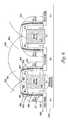
- FIG. 6illustrates a cross-sectional view of yet another alternate embodiment of a vertical NOR NROM memory array of the present invention using ultra-thin SOI.
- This figureillustrates four vertical transistors 650 - 653 .
- the transistors formed around the first oxide pillar 632are described.
- the remaining transistorsare substantially identical in structure and operation.
- the two ultra-thin silicon body regions 608 and 609are formed by epitaxial regrowth along the sidewalls of the oxide pillar 632 .
- the gate insulator layers 601 and 602are formed alongside of the silicon body regions 608 and 609 .
- the n+ polysilicon gate structures 630 and 631 for each transistor 650 and 651are then formed on the insulator layers 601 and 602 .
- the nitride layers 603 and 604provide two charge storage areas 610 and 611 for each transistor 650 - 653 .
- the lower oxide layer 605has a thicker composition than the rest of the gate insulator layer.
- the above cells 650 - 653are formed on a lower n+ region 620 on the substrate that acts as a common source/drain area, depending on the direction that each transistor is biased.
- the upper n+ regions 660 and 661are the second common source/drain area for each transistor 650 and 651 .
- the upper n+ region 660 and 661 of each transistoris coupled to other transistors in the array by a bonding wire 640 or other conductive device.
- FIG. 7illustrates an electrical equivalent circuit of a NOR NROM flash memory array of the present invention in accordance with the embodiment of FIG. 6 .
- This figureillustrates the respective cells 650 - 653 as described in FIG. 6 above.
- the control gates 701 - 704are coupled to other cells in the array and act as word lines. Two of these control gates 701 - 704 are illustrated in FIG. 6 as 630 and 631 .
- the top common source/drain areas 660 and 661are shown as virtual ground or data bit line 709 while the common source/drain area 620 is shown as virtual ground or data bit line 708 .
- FIG. 8illustrates a cross-sectional view of one embodiment of a planar NAND NROM cell of the present invention using ultra-thin SOI.
- This embodimentis comprised of the two source/drain regions 803 and 804 with the fully depleted body region 801 in the ultra-thin SOI.
- the two oxide regions 807 and 808are formed above the n+ areas and the gate insulator 805 is formed over this architecture.
- the gate insulator 805is a composite ONO layer but can be any other type of material including those described above.
- the control gate 806is formed above the gate insulator 805 .
- the gate 806extends in the ‘z’ direction instead of the ‘x’ direction as in the NOR embodiment.
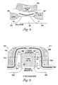
- FIG. 9illustrates a cross-sectional view of one embodiment of two vertical NAND NROM cells 910 and 911 of the present invention using ultra-thin SOI.
- Each transistor 910 and 911is comprised of a source/drain region 905 and 906 formed in a p-type substrate material.
- Second source/drain regions 920 and 921are formed on top of the oxide pillar 930 and separated by the grain boundary while still electrically coupled.
- the source/drain regions 905 , 906 , 920 , and 921function as electrical connections down the row.
- Epitaxial regrowthis used to grow ultra-thin silicon body regions 901 and 902 on the sidewalls of the oxide pillar 930 . As in previous embodiments, these regions 901 and 902 are each less than 100 nm thick.
- the gate insulator 950is formed on top of the transistors 910 and 911 .
- the gate insulator 950is an ONO composite layer. Alternate embodiments for the composition of this layer have been illustrated previously.
- Control gates 907 and 908 for each transistor 910 and 911 respectivelyare formed from a polysilicon material on each side of the gate insulator 950 .
- the control gates 907 and 908are coupled to other transistors to act as word lines.
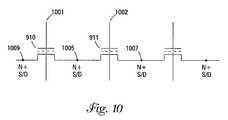
- FIG. 10illustrates an electrical equivalent circuit of a NAND NROM flash memory array of the present invention in accordance with the embodiment of FIG. 9 .
- the two transistors 910 and 911 of FIG. 9are shown.
- the n+ source/drain connection 1005 of FIG. 10corresponds to the two source/drain regions 920 and 921 of FIG. 9 .
- the word lines 1001 and 1002 of FIG. 10correspond to the control gate 907 and 908 respectively of FIG. 9 .
- the source/drain regions 905 and 906 formed in the substrate of FIG. 9correspond to the source/drain connections 1009 and 1007 of FIG. 10 .
- FIG. 11illustrates a functional block diagram of a memory device 1100 that can incorporate the ultra-thin SOI flash memory cells of the present invention.
- the memory device 1100is coupled to a processor 1110 .
- the processor 1110may be a microprocessor or some other type of controlling circuitry.
- the memory device 1100 and the processor 1110form part of an electronic system 1120 .
- the memory device 1100has been simplified to focus on features of the memory that are helpful in understanding the present invention.
- the memory deviceincludes an array of flash memory cells 1130 .
- the memory cellsare NROM flash memory cells and the memory array 1130 is arranged in banks of rows and columns.
- the control gates of each row of memory cellsis coupled with a wordline while the drain and source connections of the memory cells are coupled to bitlines.
- bitlinesAs is well known in the art, the connection of the cells to the bitlines depends on whether the array is a NAND architecture or a NOR architecture.
- An address buffer circuit 1140is provided to latch address signals provided on address input connections A 0 -Ax 1142 . Address signals are received and decoded by a row decoder 1144 and a column decoder 1146 to access the memory array 1130 . It will be appreciated by those skilled in the art, with the benefit of the present description, that the number of address input connections depends on the density and architecture of the memory array 1130 . That is, the number of addresses increases with both increased memory cell counts and increased bank and block counts.
- the memory device 1100reads data in the memory array 1130 by sensing voltage or current changes in the memory array columns using sense/buffer circuitry 1150 .
- the sense/buffer circuitryin one embodiment, is coupled to read and latch a row of data from the memory array 1130 .
- Data input and output buffer circuitry 1160is included for bi-directional data communication over a plurality of data connections 1162 with the controller 1110 ).
- Write circuitry 1155is provided to write data to the memory array.
- Control circuitry 1170decodes signals provided on control connections 1172 from the processor 1110 . These signals are used to control the operations on the memory array 1130 , including data read, data write, and erase operations.
- the control circuitry 1170may be a state machine, a sequencer, or some other type of controller.
- the memory device 1100 of FIG. 11may be an embedded device with a CMOS processor.
- the flash memory device illustrated in FIG. 11has been simplified to facilitate a basic understanding of the features of the memory. A more detailed understanding of internal circuitry and functions of flash memories are known to those skilled in the art.
- the NROM flash memory cells of the present inventionutilize ultra-thin SOI to provide a fully depleted body region. This eliminates the undesirable floating body effects experienced by partially depleted CMOS devices.
Landscapes
- Engineering & Computer Science (AREA)
- Computer Hardware Design (AREA)
- Power Engineering (AREA)
- Microelectronics & Electronic Packaging (AREA)
- Physics & Mathematics (AREA)
- Manufacturing & Machinery (AREA)
- Condensed Matter Physics & Semiconductors (AREA)
- General Physics & Mathematics (AREA)
- Chemical Kinetics & Catalysis (AREA)
- Chemical & Material Sciences (AREA)
- General Chemical & Material Sciences (AREA)
- Crystallography & Structural Chemistry (AREA)
- Non-Volatile Memory (AREA)
- Semiconductor Memories (AREA)
- Thin Film Transistor (AREA)
Abstract
Description
- This Application is a Continuation of U.S. application Ser. No. 10/714,753, titled “NROM FLASH MEMORY DEVICES ON ULTRATHIN SILICON,” filed Nov. 17, 2003, (pending) which is commonly assigned and incorporated herein by reference.
- The present invention relates generally to memory devices and in particular the present invention relates to nitride read only memory flash memory devices.
- The increased speed and capability of computers and other electronic devices requires better performance from the integrated circuits that make up a device. One way to make the integrated circuits faster is to reduce the size of the transistors that make up the device. However, as transistors are made smaller and faster, delays through the connections between the transistors becomes greater in relation to the speed of the transistor.
- An alternative technique to speed up integrated circuits is to use alternative semiconductors. For example, silicon-on-insulator (SOI) technology provides a 25-35% performance increase over equivalent CMOS technologies. SOI refers to placing a thin layer of silicon on top of an insulator such as silicon oxide or glass. The transistors would then be built on this thin layer of SOI. The SOI layer reduces the capacitance of the transistors so that they operate faster.
FIG. 1 illustrates a typical prior art SOI semiconductor. The transistor is formed in thesilicon layer 101 that is over theinsulator 102. The insulator is formed on top of thesubstrate 103. Within thesilicon layer 101, the drain/source regions gate 107 is formed above the partiallydepleted channel 109. Afloating body 110 is within thedepleted region 112 and results from the partial depletion.- SOI technology, however, imposes significant technical challenges. The silicon film used for SOI transistors must be perfect crystalline silicon. The insulator layer, however, is not crystalline. It is very difficult to make perfect crystalline silicon-on-oxide or silicon with other insulators since the insulator layer's crystalline properties are so different from the pure silicon. If perfect crystalline silicon is not obtained, defects will find their way onto the SOI film. This degrades the transistor performance.
- Additionally, floating body effects in partially depleted CMOS devices using SOI technology are undesirable in many logic and memory applications. The floating bodies cause threshold voltages and switching speeds to be variable and complex functions of the switching history of a particular logic gate. In dynamic logic and DRAM memories, the floating bodies cause excess charge leakage and short retention times that can cause data loss. In conventional flash memories and NROM devices, the floating bodies cause reduced erase fields and slower erase times.
- For the reasons stated above, and for other reasons stated below which will become apparent to those skilled in the art upon reading and understanding the present specification, there is a need in the art for a way to eliminate floating body effects in CMOS devices incorporating SOI technology.
- The above-mentioned problems with eliminating floating body effects and other problems are addressed by the present invention and will be understood by reading and studying the following specification.
- The present invention encompasses an NROM transistor having an ultra-thin silicon-on-insulator substrate. The silicon has two doped source/drain regions separated by a normally fully depleted body region. The doped regions are a different conductivity than the substrate.
- An oxide layer is formed above each of the source/drain regions. A gate insulator is formed over the body region and oxide layer. The gate insulator is capable of storing a plurality of charges. A control gate is formed on the gate insulator.
- Further embodiments of the invention include methods and apparatus of varying scope.
FIG. 1 shows a cross-sectional view of a typical prior art SOI semiconductor.FIG. 2 shows a cross-sectional view of one embodiment for a planar NOR NROM cell using ultra-thin SOI.FIG. 3 shows a cross-sectional view of one embodiment of two vertical NOR NROM cells of the present invention using ultra-thin SOI.FIG. 4 shows a cross-sectional view of another embodiment of two vertical NOR NROM cells of the present invention using ultra-thin SOI.FIG. 5 shows an electrical equivalent circuit of a NOR NROM flash memory array of the present invention.FIG. 6 shows a cross-sectional view of yet another alternate embodiment of a vertical NOR NROM memory array of the present invention using ultra-thin SOI.FIG. 7 shows an electrical equivalent circuit of a NOR NROM flash memory array of the present invention in accordance with the embodiment ofFIG. 6 .FIG. 8 shows a cross-sectional view of one embodiment of a planar NAND NROM cell of the present invention using ultra-thin SOI.FIG. 9 shows a cross-sectional view of one embodiment of two vertical NAND NROM cells of the present invention using ultra-thin SOI.FIG. 10 shows an electrical equivalent circuit of a NAND NROM flash memory array of the present invention in accordance with the embodiment ofFIG. 9 .FIG. 11 shows a block diagram of one embodiment of an electronic system of the present invention.- In the following detailed description of the invention, reference is made to the accompanying drawings that form a part hereof and in which is shown, by way of illustration, specific embodiments in which the invention may be practiced. In the drawings, like numerals describe substantially similar components throughout the several views. These embodiments are described in sufficient detail to enable those skilled in the art to practice the invention. Other embodiments may be utilized and structural, logical, and electrical changes may be made without departing from the scope of the present invention. The following detailed description is, therefore, not to be taken in a limiting sense, and the scope of the present invention is defined only by the appended claims and equivalents thereof.
FIG. 2 illustrates a cross-sectional view of one embodiment of a planar NROM cell using ultra-thin silicon-on-insulator (SOI) technology. The NROM flash memory cell ofFIG. 2 is a NOR array cell with virtual ground bit lines.- The NROM flash memory cell is comprised of the
silicon layer 201 on theinsulator 202. Thesilicon 201 in an ultra-thin SOI cell is less than 100 nm (1000 Å). Thislayer 201 is comprised of two source/drain areas bit lines areas - The
body region 200 between thebit lines body region 200 is comprised of ionizedacceptor impurities 203 and ionizeddonor impurities 205. Twooxide areas silicon 201. - A
gate insulator 207, in one embodiment, is a composite structure of oxide-nitride-oxide (ONO) formed between thecontrol gate 230 and thesilicon layer 201. Thecontrol gate 230, in one embodiment, is a polysilicon material and extends in the ‘x’ direction in the NOR flash cell embodiment. Thenitride layer 225 has twocharge storage areas - Alternate embodiments of the present invention use other gate insulators besides the ONO composite structure shown. These structures may include oxide-nitride-aluminum oxide composite layers, oxide- aluminum oxide-oxide composite layers, oxide, silicon oxycarbide-oxide composite layers as well as other composite layers.
- In still other alternate embodiments, the gate insulator may include thicker than normal silicon oxides formed by wet oxidation and not annealed, silicon rich oxides with inclusions of nanoparticles of silicon, silicon oxynitride layer that are not composite layers, silicon rich aluminum oxide insulators that are not composite layers, silicon oxycarbide insulators that are not composite layers, silicon oxide insulators with inclusions of nanoparticles of silicon carbide, in addition to other non-stoichiometric single layers of gate insulators of two or more commonly used insulator materials such as Si, N, Al, Ti, Ta, Hf, Zr, and La.
FIG. 3 illustrates a cross-sectional view of one embodiment of two vertical NORNROM cells - The
cells FIG. 3 each have source/drain areas drain areas vertical oxide pillar 310. Theleft transistor 350 uses source/drain areas drain areas drain areas vertical oxide pillar 310 is an insulator between the twotransistors - Vertical epitaxial regrowth of amorphous layers is used to provide crystalline layers of
ultra-thin silicon vertical oxide pillar 310. These layers are the ultra-thin silicon (i.e., <100 nm)body regions silicon body region left transistor 350 while theright body region 300 is part of theright transistor 351. - The
gate insulator layer 307, in one embodiment, is a composite ONO structure. Alternate embodiments of thislayer 307 are disclosed above. Thecontrol gate 330 is formed above thisinsulator layer 307 and is common to bothtransistors control gate 330 is a polysilicon material. FIG. 4 illustrates a cross-sectional view of another embodiment of two vertical NOR NROM cells of the present invention using ultra-thin SOI. This embodiment has an architecture that is substantially similar to the embodiment ofFIG. 3 in that the ultra-thinsilicon body regions oxide pillar 410. The top source/drain areas oxide pillar 410 and the commonpoly control gate 405 is formed over thegate insulator 420 coupling bothtransistors - However, in the embodiment of
FIG. 4 , thebottom oxide layer gate insulator 420 is thicker in the trench than in the previous embodiment. Additionally, the two source/drain areas ofFIG. 3 are replaced by a single n+ source/drain region 430 that is isolated between the portions of the thicker oxide layer. FIG. 5 illustrates an electrical equivalent circuit of a NOR NROM flash memory array of the present invention. This circuit can represent the planar embodiments of the present invention as well as the vertical embodiment ofFIG. 3 .- The
control gate 501 crosses all of the devices510-512 in the array. The n+ source/drain regions control gate 501 is the word line used to select the cells510-512. FIG. 6 illustrates a cross-sectional view of yet another alternate embodiment of a vertical NOR NROM memory array of the present invention using ultra-thin SOI. This figure illustrates four vertical transistors650-653. For purposes of clarity, only the transistors formed around thefirst oxide pillar 632 are described. The remaining transistors are substantially identical in structure and operation.- As in previous embodiments, the two ultra-thin
silicon body regions oxide pillar 632. The gate insulator layers601 and602 are formed alongside of thesilicon body regions polysilicon gate structures transistor - The nitride layers603 and604 provide two
charge storage areas lower oxide layer 605 has a thicker composition than the rest of the gate insulator layer. The above cells650-653 are formed on alower n+ region 620 on the substrate that acts as a common source/drain area, depending on the direction that each transistor is biased. - The
upper n+ regions transistor upper n+ region bonding wire 640 or other conductive device. FIG. 7 illustrates an electrical equivalent circuit of a NOR NROM flash memory array of the present invention in accordance with the embodiment ofFIG. 6 . This figure illustrates the respective cells650-653 as described inFIG. 6 above.- The control gates701-704 are coupled to other cells in the array and act as word lines. Two of these control gates701-704 are illustrated in
FIG. 6 as630 and631. The top common source/drain areas data bit line 709 while the common source/drain area 620 is shown as virtual ground ordata bit line 708. FIG. 8 illustrates a cross-sectional view of one embodiment of a planar NAND NROM cell of the present invention using ultra-thin SOI. This embodiment is comprised of the two source/drain regions 803 and804 with the fully depletedbody region 801 in the ultra-thin SOI. The twooxide regions gate insulator 805 is formed over this architecture. In one embodiment, thegate insulator 805 is a composite ONO layer but can be any other type of material including those described above.- The
control gate 806 is formed above thegate insulator 805. In the NAND embodiment, thegate 806 extends in the ‘z’ direction instead of the ‘x’ direction as in the NOR embodiment. FIG. 9 illustrates a cross-sectional view of one embodiment of two verticalNAND NROM cells transistor drain region drain regions oxide pillar 930 and separated by the grain boundary while still electrically coupled. The source/drain regions - Epitaxial regrowth is used to grow ultra-thin
silicon body regions oxide pillar 930. As in previous embodiments, theseregions - The
gate insulator 950 is formed on top of thetransistors gate insulator 950 is an ONO composite layer. Alternate embodiments for the composition of this layer have been illustrated previously. Control gates transistor gate insulator 950. Thecontrol gates FIG. 10 illustrates an electrical equivalent circuit of a NAND NROM flash memory array of the present invention in accordance with the embodiment ofFIG. 9 . The twotransistors FIG. 9 are shown.- The n+ source/
drain connection 1005 ofFIG. 10 corresponds to the two source/drain regions FIG. 9 . The word lines1001 and1002 ofFIG. 10 correspond to thecontrol gate FIG. 9 . The source/drain regions FIG. 9 correspond to the source/drain connections FIG. 10 . - The above embodiments are illustrated as n-channel type transistors. However, one of ordinary skill in the art will understand that the conductivity types can be reversed by altering the doping types such that the present invention is equally applicable to include structures NROM structures having ultra-thin silicon, p-channel type transistors.
- The masking and etching steps used to form the ultra-thin silicon NROM flash memory cells of the present invention are not discussed in detail. The various steps required to form the above-described architectures are well known by those skilled in the art.
FIG. 11 illustrates a functional block diagram of amemory device 1100 that can incorporate the ultra-thin SOI flash memory cells of the present invention. Thememory device 1100 is coupled to aprocessor 1110. Theprocessor 1110 may be a microprocessor or some other type of controlling circuitry. Thememory device 1100 and theprocessor 1110 form part of anelectronic system 1120. Thememory device 1100 has been simplified to focus on features of the memory that are helpful in understanding the present invention.- The memory device includes an array of
flash memory cells 1130. In one embodiment, the memory cells are NROM flash memory cells and thememory array 1130 is arranged in banks of rows and columns. The control gates of each row of memory cells is coupled with a wordline while the drain and source connections of the memory cells are coupled to bitlines. As is well known in the art, the connection of the cells to the bitlines depends on whether the array is a NAND architecture or a NOR architecture. - An
address buffer circuit 1140 is provided to latch address signals provided on address input connections A0-Ax 1142. Address signals are received and decoded by arow decoder 1144 and acolumn decoder 1146 to access thememory array 1130. It will be appreciated by those skilled in the art, with the benefit of the present description, that the number of address input connections depends on the density and architecture of thememory array 1130. That is, the number of addresses increases with both increased memory cell counts and increased bank and block counts. - The
memory device 1100 reads data in thememory array 1130 by sensing voltage or current changes in the memory array columns using sense/buffer circuitry 1150. The sense/buffer circuitry, in one embodiment, is coupled to read and latch a row of data from thememory array 1130. Data input andoutput buffer circuitry 1160 is included for bi-directional data communication over a plurality ofdata connections 1162 with the controller1110).Write circuitry 1155 is provided to write data to the memory array. Control circuitry 1170 decodes signals provided oncontrol connections 1172 from theprocessor 1110. These signals are used to control the operations on thememory array 1130, including data read, data write, and erase operations. Thecontrol circuitry 1170 may be a state machine, a sequencer, or some other type of controller.- Since the NROM memory cells of the present invention use a CMOS compatible process, the
memory device 1100 ofFIG. 11 may be an embedded device with a CMOS processor. - The flash memory device illustrated in
FIG. 11 has been simplified to facilitate a basic understanding of the features of the memory. A more detailed understanding of internal circuitry and functions of flash memories are known to those skilled in the art. - In summary, the NROM flash memory cells of the present invention utilize ultra-thin SOI to provide a fully depleted body region. This eliminates the undesirable floating body effects experienced by partially depleted CMOS devices.
- Although specific embodiments have been illustrated and described herein, it will be appreciated by those of ordinary skill in the art that any arrangement that is calculated to achieve the same purpose may be substituted for the specific embodiments shown. Many adaptations of the invention will be apparent to those of ordinary skill in the art. Accordingly, this application is intended to cover any adaptations or variations of the invention. It is manifestly intended that this invention be limited only by the following claims and equivalents thereof.
Claims (20)
Priority Applications (1)
| Application Number | Priority Date | Filing Date | Title |
|---|---|---|---|
| US11/211,208US7244987B2 (en) | 2003-11-17 | 2005-08-25 | NROM flash memory devices on ultrathin silicon |
Applications Claiming Priority (2)
| Application Number | Priority Date | Filing Date | Title |
|---|---|---|---|
| US10/714,753US7202523B2 (en) | 2003-11-17 | 2003-11-17 | NROM flash memory devices on ultrathin silicon |
| US11/211,208US7244987B2 (en) | 2003-11-17 | 2005-08-25 | NROM flash memory devices on ultrathin silicon |
Related Parent Applications (1)
| Application Number | Title | Priority Date | Filing Date |
|---|---|---|---|
| US10/714,753DivisionUS7202523B2 (en) | 2003-11-17 | 2003-11-17 | NROM flash memory devices on ultrathin silicon |
Publications (2)
| Publication Number | Publication Date |
|---|---|
| US20050280089A1true US20050280089A1 (en) | 2005-12-22 |
| US7244987B2 US7244987B2 (en) | 2007-07-17 |
Family
ID=34574051
Family Applications (9)
| Application Number | Title | Priority Date | Filing Date |
|---|---|---|---|
| US10/714,753Expired - LifetimeUS7202523B2 (en) | 2003-11-17 | 2003-11-17 | NROM flash memory devices on ultrathin silicon |
| US11/211,207Expired - LifetimeUS7276413B2 (en) | 2003-11-17 | 2005-08-25 | NROM flash memory devices on ultrathin silicon |
| US11/211,208Expired - LifetimeUS7244987B2 (en) | 2003-11-17 | 2005-08-25 | NROM flash memory devices on ultrathin silicon |
| US11/211,201Expired - LifetimeUS7276762B2 (en) | 2003-11-17 | 2005-08-25 | NROM flash memory devices on ultrathin silicon |
| US11/693,150Expired - LifetimeUS7358562B2 (en) | 2003-11-17 | 2007-03-29 | NROM flash memory devices on ultrathin silicon |
| US11/693,105Expired - LifetimeUS7378316B2 (en) | 2003-11-17 | 2007-03-29 | Method for fabricating semiconductor vertical NROM memory cells |
| US12/114,897Expired - LifetimeUS7768058B2 (en) | 2003-11-17 | 2008-05-05 | NROM flash memory devices on ultrathin silicon |
| US12/829,702Expired - LifetimeUS7915669B2 (en) | 2003-11-17 | 2010-07-02 | NROM flash memory devices on ultrathin silicon |
| US13/051,050Expired - Fee RelatedUS8183625B2 (en) | 2003-11-17 | 2011-03-18 | NROM flash memory devices on ultrathin silicon |
Family Applications Before (2)
| Application Number | Title | Priority Date | Filing Date |
|---|---|---|---|
| US10/714,753Expired - LifetimeUS7202523B2 (en) | 2003-11-17 | 2003-11-17 | NROM flash memory devices on ultrathin silicon |
| US11/211,207Expired - LifetimeUS7276413B2 (en) | 2003-11-17 | 2005-08-25 | NROM flash memory devices on ultrathin silicon |
Family Applications After (6)
| Application Number | Title | Priority Date | Filing Date |
|---|---|---|---|
| US11/211,201Expired - LifetimeUS7276762B2 (en) | 2003-11-17 | 2005-08-25 | NROM flash memory devices on ultrathin silicon |
| US11/693,150Expired - LifetimeUS7358562B2 (en) | 2003-11-17 | 2007-03-29 | NROM flash memory devices on ultrathin silicon |
| US11/693,105Expired - LifetimeUS7378316B2 (en) | 2003-11-17 | 2007-03-29 | Method for fabricating semiconductor vertical NROM memory cells |
| US12/114,897Expired - LifetimeUS7768058B2 (en) | 2003-11-17 | 2008-05-05 | NROM flash memory devices on ultrathin silicon |
| US12/829,702Expired - LifetimeUS7915669B2 (en) | 2003-11-17 | 2010-07-02 | NROM flash memory devices on ultrathin silicon |
| US13/051,050Expired - Fee RelatedUS8183625B2 (en) | 2003-11-17 | 2011-03-18 | NROM flash memory devices on ultrathin silicon |
Country Status (7)
| Country | Link |
|---|---|
| US (9) | US7202523B2 (en) |
| EP (1) | EP1692728B1 (en) |
| JP (1) | JP2007534161A (en) |
| KR (2) | KR100813374B1 (en) |
| CN (1) | CN1883054A (en) |
| SG (1) | SG141431A1 (en) |
| WO (1) | WO2005050740A2 (en) |
Cited By (20)
| Publication number | Priority date | Publication date | Assignee | Title |
|---|---|---|---|---|
| US20070020840A1 (en)* | 2005-07-25 | 2007-01-25 | Freescale Semiconductor, Inc. | Programmable structure including nanocrystal storage elements in a trench |
| US20070018232A1 (en)* | 2005-07-25 | 2007-01-25 | Freescale Semiconductor, Inc. | Nonvolatile storage array with continuous control gate employing hot carrier injection programming |
| US20070020831A1 (en)* | 2005-07-25 | 2007-01-25 | Freescale Semiconductor, Inc. | Method of fabricating a nonvolatile storage array with continuous control gate employing hot carrier injection programming |
| US20070018234A1 (en)* | 2005-07-25 | 2007-01-25 | Freescale Semiconductor, Inc. | Electronic device including gate lines, bit lines, or a combination thereof |
| US20070018222A1 (en)* | 2005-07-25 | 2007-01-25 | Freescale Semiconductor, Inc. | Electronic device including discontinuous storage elements |
| US20070018229A1 (en)* | 2005-07-25 | 2007-01-25 | Freescale Semiconductor, Inc. | Electronic device including discontinuous storage elements and a process for forming the same |
| US20070020851A1 (en)* | 2005-07-25 | 2007-01-25 | Freescale Semiconductor, Inc. | Hot carrier injection programmable structure including discontinuous storage elements and spacer control gates in a trench and a method of using the same |
| US20070020845A1 (en)* | 2005-07-25 | 2007-01-25 | Freescale Semiconductor, Inc. | Method of fabricating programmable structure including discontinuous storage elements and spacer control gates in a trench |
| US20070020856A1 (en)* | 2005-07-25 | 2007-01-25 | Freescale Semiconductor, Inc. | Process for forming an electronic device including discontinuous storage elements |
| US20070018207A1 (en)* | 2005-07-25 | 2007-01-25 | Freescale Semiconductor, Inc. | Split gate storage device including a horizontal first gate and a vertical second gate in a trench |
| US20070020820A1 (en)* | 2005-07-25 | 2007-01-25 | Freescale Semiconductor, Inc. | Process for forming an electronic device including discontinuous storage elements |
| US20070019472A1 (en)* | 2005-07-25 | 2007-01-25 | Freescale Semiconductor, Inc. | Electronic device including a memory array and conductive lines |
| US20070020857A1 (en)* | 2005-07-25 | 2007-01-25 | Freescale Semiconductor, Inc. | Process for forming an electronic device including discontinuous storage elements |
| US20070018240A1 (en)* | 2005-07-25 | 2007-01-25 | Freescale Semiconductor, Inc. | Electronic device including discontinuous storage elements |
| US20070018221A1 (en)* | 2005-07-25 | 2007-01-25 | Freescale Semiconductor, Inc. | Programmable structure including discontinuous storage elements and spacer control gates in a trench |
| US20070018216A1 (en)* | 2005-07-25 | 2007-01-25 | Freescale Semiconductor, Inc. | Electronic device including discontinuous storage elements |
| US20080173923A1 (en)* | 2007-01-24 | 2008-07-24 | Freescale Semiconductor, Inc. | Electronic device including trenches and discontinuous storage elements and processes of forming and using the same |
| US20080173922A1 (en)* | 2007-01-24 | 2008-07-24 | Freescale Semiconductor, Inc. | Electronic device including fins and discontinuous storage elements and processes of forming and using the same |
| US20080173921A1 (en)* | 2007-01-24 | 2008-07-24 | Freescale Semiconductor, Inc. | Electronic device including trenches and discontinuous storage elements and processes of forming and using the same |
| US20080199996A1 (en)* | 2007-02-19 | 2008-08-21 | Ramachandran Muralidhar | Method for forming a split gate memory device |
Families Citing this family (31)
| Publication number | Priority date | Publication date | Assignee | Title |
|---|---|---|---|---|
| US7202523B2 (en)* | 2003-11-17 | 2007-04-10 | Micron Technology, Inc. | NROM flash memory devices on ultrathin silicon |
| US7183166B2 (en)* | 2003-11-25 | 2007-02-27 | Macronix International Co., Ltd. | Method for forming oxide on ONO structure |
| US20050156228A1 (en)* | 2004-01-16 | 2005-07-21 | Jeng Erik S. | Manufacture method and structure of a nonvolatile memory |
| KR100564628B1 (en)* | 2004-06-16 | 2006-03-28 | 삼성전자주식회사 | Split gate type flash memory device and manufacturing method thereof |
| US7138681B2 (en)* | 2004-07-27 | 2006-11-21 | Micron Technology, Inc. | High density stepped, non-planar nitride read only memory |
| US7518179B2 (en) | 2004-10-08 | 2009-04-14 | Freescale Semiconductor, Inc. | Virtual ground memory array and method therefor |
| KR100630746B1 (en)* | 2005-05-06 | 2006-10-02 | 삼성전자주식회사 | Multi-bit and multi-level nonvolatile memory device and its operation and manufacturing method |
| US7439576B2 (en)* | 2005-08-29 | 2008-10-21 | Micron Technology, Inc. | Ultra-thin body vertical tunneling transistor |
| US7446372B2 (en)* | 2005-09-01 | 2008-11-04 | Micron Technology, Inc. | DRAM tunneling access transistor |
| KR100685121B1 (en)* | 2005-10-14 | 2007-02-22 | 동부일렉트로닉스 주식회사 | Nonvolatile Memory Device and Manufacturing Method Thereof |
| US20070246765A1 (en)* | 2006-03-30 | 2007-10-25 | Lars Bach | Semiconductor memory device and method for production |
| US7592224B2 (en) | 2006-03-30 | 2009-09-22 | Freescale Semiconductor, Inc | Method of fabricating a storage device including decontinuous storage elements within and between trenches |
| JP5248819B2 (en)* | 2006-08-07 | 2013-07-31 | 三星電子株式会社 | Transistor and manufacturing method thereof |
| JP2008053270A (en)* | 2006-08-22 | 2008-03-06 | Nec Electronics Corp | Semiconductor memory device and manufacturing method thereof |
| US7880232B2 (en)* | 2006-11-01 | 2011-02-01 | Micron Technology, Inc. | Processes and apparatus having a semiconductor fin |
| JP2008166442A (en)* | 2006-12-27 | 2008-07-17 | Spansion Llc | Semiconductor device and manufacturing method thereof |
| US7790560B2 (en)* | 2007-03-12 | 2010-09-07 | Board Of Regents Of The Nevada System Of Higher Education | Construction of flash memory chips and circuits from ordered nanoparticles |
| US8686487B2 (en) | 2007-06-14 | 2014-04-01 | Micron Technology, Inc. | Semiconductor devices and electronic systems comprising floating gate transistors |
| US7737488B2 (en)* | 2007-08-09 | 2010-06-15 | Macronix International Co., Ltd. | Blocking dielectric engineered charge trapping memory cell with high speed erase |
| US8320191B2 (en) | 2007-08-30 | 2012-11-27 | Infineon Technologies Ag | Memory cell arrangement, method for controlling a memory cell, memory array and electronic device |
| US8409952B2 (en)* | 2008-04-14 | 2013-04-02 | Spansion Llc | Method of forming an electronic device including forming a charge storage element in a trench of a workpiece |
| US8551858B2 (en)* | 2010-02-03 | 2013-10-08 | Spansion Llc | Self-aligned SI rich nitride charge trap layer isolation for charge trap flash memory |
| US8207032B2 (en) | 2010-08-31 | 2012-06-26 | Micron Technology, Inc. | Methods of forming pluralities of vertical transistors, and methods of forming memory arrays |
| CN102769016B (en)* | 2012-08-14 | 2015-01-14 | 北京大学 | Anti-radiation complementary metal oxide semiconductor (CMOS) device and preparation method thereof |
| KR102050561B1 (en)* | 2012-12-18 | 2020-01-09 | 삼성디스플레이 주식회사 | Vertical thin film transistor and fabrivating method thereof |
| US9093530B2 (en) | 2012-12-28 | 2015-07-28 | Taiwan Semiconductor Manufacturing Company, Ltd. | Fin structure of FinFET |
| US9082735B1 (en)* | 2014-08-14 | 2015-07-14 | Srikanth Sundararajan | 3-D silicon on glass based organic light emitting diode display |
| JP6100854B2 (en)* | 2014-11-19 | 2017-03-22 | 株式会社日立国際電気 | Semiconductor device manufacturing method, substrate processing apparatus, gas supply system, and program |
| US9385240B1 (en)* | 2015-03-03 | 2016-07-05 | Macronix International Co., Ltd. | Memory device and method for fabricating the same |
| US20170345834A1 (en)* | 2016-05-25 | 2017-11-30 | Globalfoundries Inc. | Soi memory device |
| US10199464B2 (en) | 2017-02-21 | 2019-02-05 | International Business Machines Corporation | Techniques for VFET top source/drain epitaxy |
Citations (91)
| Publication number | Priority date | Publication date | Assignee | Title |
|---|---|---|---|---|
| US4184207A (en)* | 1978-01-27 | 1980-01-15 | Texas Instruments Incorporated | High density floating gate electrically programmable ROM |
| US4420504A (en)* | 1980-12-22 | 1983-12-13 | Raytheon Company | Programmable read only memory |
| US4755864A (en)* | 1984-12-25 | 1988-07-05 | Kabushiki Kaisha Toshiba | Semiconductor read only memory device with selectively present mask layer |
| US4881114A (en)* | 1986-05-16 | 1989-11-14 | Actel Corporation | Selectively formable vertical diode circuit element |
| US5241496A (en)* | 1991-08-19 | 1993-08-31 | Micron Technology, Inc. | Array of read-only memory cells, eacch of which has a one-time, voltage-programmable antifuse element constructed within a trench shared by a pair of cells |
| US5330930A (en)* | 1992-12-31 | 1994-07-19 | Chartered Semiconductor Manufacturing Pte Ltd. | Formation of vertical polysilicon resistor having a nitride sidewall for small static RAM cell |
| US5378647A (en)* | 1993-10-25 | 1995-01-03 | United Microelectronics Corporation | Method of making a bottom gate mask ROM device |
| US5379253A (en)* | 1992-06-01 | 1995-01-03 | National Semiconductor Corporation | High density EEPROM cell array with novel programming scheme and method of manufacture |
| US5397725A (en)* | 1993-10-28 | 1995-03-14 | National Semiconductor Corporation | Method of controlling oxide thinning in an EPROM or flash memory array |
| US5467305A (en)* | 1992-03-12 | 1995-11-14 | International Business Machines Corporation | Three-dimensional direct-write EEPROM arrays and fabrication methods |
| US5576236A (en)* | 1995-06-28 | 1996-11-19 | United Microelectronics Corporation | Process for coding and code marking read-only memory |
| US5768192A (en)* | 1996-07-23 | 1998-06-16 | Saifun Semiconductors, Ltd. | Non-volatile semiconductor memory cell utilizing asymmetrical charge trapping |
| US5792697A (en)* | 1997-01-07 | 1998-08-11 | United Microelectronics Corporation | Method for fabricating a multi-stage ROM |
| US5858841A (en)* | 1997-01-20 | 1999-01-12 | United Microelectronics Corporation | ROM device having memory units arranged in three dimensions, and a method of making the same |
| US5911106A (en)* | 1996-08-29 | 1999-06-08 | Nec Corporation | Semiconductor memory device and fabrication thereof |
| US5946558A (en)* | 1997-02-05 | 1999-08-31 | United Microelectronics Corp. | Method of making ROM components |
| US5966603A (en)* | 1997-06-11 | 1999-10-12 | Saifun Semiconductors Ltd. | NROM fabrication method with a periphery portion |
| US5973358A (en)* | 1997-07-01 | 1999-10-26 | Citizen Watch Co., Ltd. | SOI device having a channel with variable thickness |
| US5994745A (en)* | 1994-04-08 | 1999-11-30 | United Microelectronics Corp. | ROM device having shaped gate electrodes and corresponding code implants |
| US6011725A (en)* | 1997-08-01 | 2000-01-04 | Saifun Semiconductors, Ltd. | Two bit non-volatile electrically erasable and programmable semiconductor memory cell utilizing asymmetrical charge trapping |
| US6028342A (en)* | 1996-11-22 | 2000-02-22 | United Microelectronics Corp. | ROM diode and a method of making the same |
| US6030871A (en)* | 1998-05-05 | 2000-02-29 | Saifun Semiconductors Ltd. | Process for producing two bit ROM cell utilizing angled implant |
| US6044022A (en)* | 1999-02-26 | 2000-03-28 | Tower Semiconductor Ltd. | Programmable configuration for EEPROMS including 2-bit non-volatile memory cell arrays |
| US6081456A (en)* | 1999-02-04 | 2000-06-27 | Tower Semiconductor Ltd. | Bit line control circuit for a memory array using 2-bit non-volatile memory cells |
| US6108240A (en)* | 1999-02-04 | 2000-08-22 | Tower Semiconductor Ltd. | Implementation of EEPROM using intermediate gate voltage to avoid disturb conditions |
| US6134156A (en)* | 1999-02-04 | 2000-10-17 | Saifun Semiconductors Ltd. | Method for initiating a retrieval procedure in virtual ground arrays |
| US6133102A (en)* | 1998-06-19 | 2000-10-17 | Wu; Shye-Lin | Method of fabricating double poly-gate high density multi-state flat mask ROM cells |
| US6147904A (en)* | 1999-02-04 | 2000-11-14 | Tower Semiconductor Ltd. | Redundancy method and structure for 2-bit non-volatile memory cells |
| US6157570A (en)* | 1999-02-04 | 2000-12-05 | Tower Semiconductor Ltd. | Program/erase endurance of EEPROM memory cells |
| US6172396B1 (en)* | 1998-02-03 | 2001-01-09 | Worldwide Semiconductor Manufacturing Corp. | ROM structure and method of manufacture |
| US6174758B1 (en)* | 1999-03-03 | 2001-01-16 | Tower Semiconductor Ltd. | Semiconductor chip having fieldless array with salicide gates and methods for making same |
| US6175523B1 (en)* | 1999-10-25 | 2001-01-16 | Advanced Micro Devices, Inc | Precharging mechanism and method for NAND-based flash memory devices |
| US6181597B1 (en)* | 1999-02-04 | 2001-01-30 | Tower Semiconductor Ltd. | EEPROM array using 2-bit non-volatile memory cells with serial read operations |
| US6184089B1 (en)* | 1999-01-27 | 2001-02-06 | United Microelectronics Corp. | Method of fabricating one-time programmable read only memory |
| US6201737B1 (en)* | 2000-01-28 | 2001-03-13 | Advanced Micro Devices, Inc. | Apparatus and method to characterize the threshold distribution in an NROM virtual ground array |
| US6204529B1 (en)* | 1999-08-27 | 2001-03-20 | Hsing Lan Lung | 8 bit per cell non-volatile semiconductor memory structure utilizing trench technology and dielectric floating gate |
| US6208557B1 (en)* | 1999-05-21 | 2001-03-27 | National Semiconductor Corporation | EPROM and flash memory cells with source-side injection and a gate dielectric that traps hot electrons during programming |
| US6207504B1 (en)* | 1998-07-29 | 2001-03-27 | United Semiconductor Corp. | Method of fabricating flash erasable programmable read only memory |
| US6215702B1 (en)* | 2000-02-16 | 2001-04-10 | Advanced Micro Devices, Inc. | Method of maintaining constant erasing speeds for non-volatile memory cells |
| US6218695B1 (en)* | 1999-06-28 | 2001-04-17 | Tower Semiconductor Ltd. | Area efficient column select circuitry for 2-bit non-volatile memory cells |
| US6222768B1 (en)* | 2000-01-28 | 2001-04-24 | Advanced Micro Devices, Inc. | Auto adjusting window placement scheme for an NROM virtual ground array |
| US20010001075A1 (en)* | 1997-03-25 | 2001-05-10 | Vantis Corporation | Process for fabricating semiconductor memory device with high data retention including silicon nitride etch stop layer formed at high temperature with low hydrogen ion concentration |
| US6240020B1 (en)* | 1999-10-25 | 2001-05-29 | Advanced Micro Devices | Method of bitline shielding in conjunction with a precharging scheme for nand-based flash memory devices |
| US6243300B1 (en)* | 2000-02-16 | 2001-06-05 | Advanced Micro Devices, Inc. | Substrate hole injection for neutralizing spillover charge generated during programming of a non-volatile memory cell |
| US20010004332A1 (en)* | 1998-05-20 | 2001-06-21 | Saifun Semiconductors Ltd. | NROM cell with improved programming, erasing and cycling |
| US6251731B1 (en)* | 1998-08-10 | 2001-06-26 | Acer Semiconductor Manufacturing, Inc. | Method for fabricating high-density and high-speed nand-type mask roms |
| US6256231B1 (en)* | 1999-02-04 | 2001-07-03 | Tower Semiconductor Ltd. | EEPROM array using 2-bit non-volatile memory cells and method of implementing same |
| US6255166B1 (en)* | 1999-08-05 | 2001-07-03 | Aalo Lsi Design & Device Technology, Inc. | Nonvolatile memory cell, method of programming the same and nonvolatile memory array |
| US6266281B1 (en)* | 2000-02-16 | 2001-07-24 | Advanced Micro Devices, Inc. | Method of erasing non-volatile memory cells |
| US6269023B1 (en)* | 2000-05-19 | 2001-07-31 | Advanced Micro Devices, Inc. | Method of programming a non-volatile memory cell using a current limiter |
| US6272043B1 (en)* | 2000-01-28 | 2001-08-07 | Advanced Micro Devices, Inc. | Apparatus and method of direct current sensing from source side in a virtual ground array |
| US6275414B1 (en)* | 2000-05-16 | 2001-08-14 | Advanced Micro Devices, Inc. | Uniform bitline strapping of a non-volatile memory cell |
| US6282118B1 (en)* | 2000-10-06 | 2001-08-28 | Macronix International Co. Ltd. | Nonvolatile semiconductor memory device |
| US6291854B1 (en)* | 1999-12-30 | 2001-09-18 | United Microelectronics Corp. | Electrically erasable and programmable read only memory device and manufacturing therefor |
| US6297096B1 (en)* | 1997-06-11 | 2001-10-02 | Saifun Semiconductors Ltd. | NROM fabrication method |
| US6303436B1 (en)* | 1999-09-21 | 2001-10-16 | Mosel Vitelic, Inc. | Method for fabricating a type of trench mask ROM cell |
| US6327174B1 (en)* | 2000-02-14 | 2001-12-04 | United Microelectronics Corp. | Method of manufacturing mask read-only memory cell |
| US6348711B1 (en)* | 1998-05-20 | 2002-02-19 | Saifun Semiconductors Ltd. | NROM cell with self-aligned programming and erasure areas |
| US20020043682A1 (en)* | 1997-08-29 | 2002-04-18 | Semiconductor Energy Laboratory Co., Ltd. | Non-volatile memory and semiconductor device |
| US6417053B1 (en)* | 2001-11-20 | 2002-07-09 | Macronix International Co., Ltd. | Fabrication method for a silicon nitride read-only memory |
| US6421275B1 (en)* | 2002-01-22 | 2002-07-16 | Macronix International Co. Ltd. | Method for adjusting a reference current of a flash nitride read only memory (NROM) and device thereof |
| US6429063B1 (en)* | 1999-10-26 | 2002-08-06 | Saifun Semiconductors Ltd. | NROM cell with generally decoupled primary and secondary injection |
| US6432778B1 (en)* | 2001-08-07 | 2002-08-13 | Macronix International Co. Ltd. | Method of forming a system on chip (SOC) with nitride read only memory (NROM) |
| US20020142569A1 (en)* | 2001-03-29 | 2002-10-03 | Chang Kent Kuohua | Method for fabricating a nitride read-only -memory (nrom) |
| US20020146885A1 (en)* | 2001-04-04 | 2002-10-10 | Chia-Hsing Chen | Method of fabricating a nitride read only memory cell |
| US20020151138A1 (en)* | 2001-04-13 | 2002-10-17 | Chien-Hung Liu | Method for fabricating an NROM |
| US6469342B1 (en)* | 2001-10-29 | 2002-10-22 | Macronix International Co., Ltd. | Silicon nitride read only memory that prevents antenna effect |
| US6468864B1 (en)* | 2001-06-21 | 2002-10-22 | Macronix International Co., Ltd. | Method of fabricating silicon nitride read only memory |
| US20020168875A1 (en)* | 2001-05-10 | 2002-11-14 | Chang Kent Kuohua | Method for fabricating an ONO layer of an NROM |
| US6486028B1 (en)* | 2001-11-20 | 2002-11-26 | Macronix International Co., Ltd. | Method of fabricating a nitride read-only-memory cell vertical structure |
| US6487050B1 (en)* | 1999-02-22 | 2002-11-26 | Seagate Technology Llc | Disc drive with wear-resistant ramp coating of carbon nitride or metal nitride |
| US20020177275A1 (en)* | 2001-05-28 | 2002-11-28 | Chien-Hung Liu | Fabrication method for a silicon nitride read-only memory |
| US20020182829A1 (en)* | 2001-05-31 | 2002-12-05 | Chia-Hsing Chen | Method for forming nitride read only memory with indium pocket region |
| US6496034B2 (en)* | 2001-02-09 | 2002-12-17 | Micron Technology, Inc. | Programmable logic arrays with ultra thin body transistors |
| US6514831B1 (en)* | 2001-11-14 | 2003-02-04 | Macronix International Co., Ltd. | Nitride read only memory cell |
| US20030040152A1 (en)* | 2001-08-22 | 2003-02-27 | Chen-Chin Liu | Method of fabricating a NROM cell to prevent charging |
| US6531887B2 (en)* | 2001-06-01 | 2003-03-11 | Macronix International Co., Ltd. | One cell programmable switch using non-volatile cell |
| US6545309B1 (en)* | 2002-03-11 | 2003-04-08 | Macronix International Co., Ltd. | Nitride read-only memory with protective diode and operating method thereof |
| US20030067807A1 (en)* | 2001-09-28 | 2003-04-10 | Hung-Sui Lin | Erasing method for p-channel NROM |
| US6552287B2 (en)* | 1999-10-08 | 2003-04-22 | Itt Manufacturing Enterprises, Inc. | Electrical switch with snap action dome shaped tripper |
| US6552387B1 (en)* | 1997-07-30 | 2003-04-22 | Saifun Semiconductors Ltd. | Non-volatile electrically erasable and programmable semiconductor memory cell utilizing asymmetrical charge trapping |
| US6559013B1 (en)* | 2002-06-20 | 2003-05-06 | Macronix International Co., Ltd. | Method for fabricating mask ROM device |
| US6576511B2 (en)* | 2001-05-02 | 2003-06-10 | Macronix International Co., Ltd. | Method for forming nitride read only memory |
| US6580135B2 (en)* | 2001-06-18 | 2003-06-17 | Macronix International Co., Ltd. | Silicon nitride read only memory structure and method of programming and erasure |
| US6580630B1 (en)* | 2002-04-02 | 2003-06-17 | Macronix International Co., Ltd. | Initialization method of P-type silicon nitride read only memory |
| US20030117861A1 (en)* | 2001-12-20 | 2003-06-26 | Eduardo Maayan | NROM NOR array |
| US6602805B2 (en)* | 2000-12-14 | 2003-08-05 | Macronix International Co., Ltd. | Method for forming gate dielectric layer in NROM |
| US6607957B1 (en)* | 2002-07-31 | 2003-08-19 | Macronix International Co., Ltd. | Method for fabricating nitride read only memory |
| US6610586B1 (en)* | 2002-09-04 | 2003-08-26 | Macronix International Co., Ltd. | Method for fabricating nitride read-only memory |
| US6617207B1 (en)* | 1999-09-17 | 2003-09-09 | Tokyo Electron Limited | Method and system for forming a stacked gate insulating film |
| US20030183873A1 (en)* | 1998-11-04 | 2003-10-02 | Ichiro Fujiwara | Nonvolatile semiconductor memory device and process of production and write method thereof |
Family Cites Families (55)
| Publication number | Priority date | Publication date | Assignee | Title |
|---|---|---|---|---|
| US4513494A (en) | 1983-07-19 | 1985-04-30 | American Microsystems, Incorporated | Late mask process for programming read only memories |
| FR2640428B1 (en)* | 1988-12-09 | 1992-10-30 | Thomson Csf | METHOD OF HARDENING WITH RESPECT TO IONIZING RADIATION OF ACTIVE ELECTRONIC COMPONENTS, AND HARDENED COMPONENTS OF LARGE DIMENSIONS |
| JP2509706B2 (en) | 1989-08-18 | 1996-06-26 | 株式会社東芝 | Mask ROM manufacturing method |
| US5547236A (en)* | 1995-02-23 | 1996-08-20 | Gregory; John E. | Removable door lock |
| JP3524213B2 (en)* | 1995-06-07 | 2004-05-10 | 株式会社ルネサステクノロジ | Semiconductor memory device and method of manufacturing the same |
| US5811852A (en)* | 1996-01-17 | 1998-09-22 | Advanced Materials Engineering Research, Inc. | Memory cell structure fabricated with improved fabrication process by forming dielectric layer directly on an insulated surface of a substrate |
| US5994765A (en)* | 1996-07-01 | 1999-11-30 | Sun Microsystems, Inc. | Clock distribution network with efficient shielding |
| US6281695B1 (en)* | 1996-12-17 | 2001-08-28 | Robbie M. K. Chung | Integrated circuit package pin indicator |
| US5990509A (en)* | 1997-01-22 | 1999-11-23 | International Business Machines Corporation | 2F-square memory cell for gigabit memory applications |
| US6034389A (en)* | 1997-01-22 | 2000-03-07 | International Business Machines Corporation | Self-aligned diffused source vertical transistors with deep trench capacitors in a 4F-square memory cell array |
| WO1998047044A1 (en)* | 1997-04-11 | 1998-10-22 | Hitachi, Ltd. | Liquid crystal display device |
| US6124729A (en)* | 1998-02-27 | 2000-09-26 | Micron Technology, Inc. | Field programmable logic arrays with vertical transistors |
| US5991225A (en)* | 1998-02-27 | 1999-11-23 | Micron Technology, Inc. | Programmable memory address decode array with vertical transistors |
| US6180461B1 (en)* | 1998-08-03 | 2001-01-30 | Halo Lsi Design & Device Technology, Inc. | Double sidewall short channel split gate flash memory |
| US6468684B1 (en)* | 1999-01-22 | 2002-10-22 | California Institute Of Technology | Proton conducting membrane using a solid acid |
| US6941644B2 (en)* | 1999-09-27 | 2005-09-13 | Reliance Electric Technologies, Llc | Method for winding segments of a segmented wound member of an electromechanical device |
| JP4923318B2 (en)* | 1999-12-17 | 2012-04-25 | ソニー株式会社 | Nonvolatile semiconductor memory device and operation method thereof |
| JP3578688B2 (en)* | 1999-12-24 | 2004-10-20 | Necエレクトロニクス株式会社 | Manufacturing method of nonvolatile memory |
| JP2001326289A (en)* | 2000-03-08 | 2001-11-22 | Semiconductor Energy Lab Co Ltd | Nonvolatile memory and semiconductor device |
| US6273043B1 (en)* | 2000-03-16 | 2001-08-14 | Raymond A. Barton | Mounting plate and rocker arm assembly |
| KR100821456B1 (en)* | 2000-08-14 | 2008-04-11 | 샌디스크 쓰리디 엘엘씨 | Dense array and charge storage device and manufacturing method thereof |
| JP4151229B2 (en)* | 2000-10-26 | 2008-09-17 | ソニー株式会社 | Nonvolatile semiconductor memory device and manufacturing method thereof |
| JP3984020B2 (en)* | 2000-10-30 | 2007-09-26 | 株式会社東芝 | Nonvolatile semiconductor memory device |
| US6664143B2 (en)* | 2000-11-22 | 2003-12-16 | North Carolina State University | Methods of fabricating vertical field effect transistors by conformal channel layer deposition on sidewalls |
| US6424001B1 (en)* | 2001-02-09 | 2002-07-23 | Micron Technology, Inc. | Flash memory with ultra thin vertical body transistors |
| US6566682B2 (en)* | 2001-02-09 | 2003-05-20 | Micron Technology, Inc. | Programmable memory address and decode circuits with ultra thin vertical body transistors |
| EP1263051A1 (en) | 2001-05-30 | 2002-12-04 | Infineon Technologies AG | Bitline contacts in a memory cell array |
| DE10138585A1 (en)* | 2001-08-06 | 2003-03-06 | Infineon Technologies Ag | memory cell |
| US6617204B2 (en) | 2001-08-13 | 2003-09-09 | Macronix International Co., Ltd. | Method of forming the protective film to prevent nitride read only memory cell charging |
| JP4198903B2 (en)* | 2001-08-31 | 2008-12-17 | 株式会社東芝 | Semiconductor memory device |
| US6903977B2 (en)* | 2001-09-25 | 2005-06-07 | Sony Corporation | Nonvolatile semiconductor memory device and method of producing the same |
| JP2003142610A (en)* | 2001-11-07 | 2003-05-16 | Sony Corp | Nonvolatile semiconductor memory device and method for injecting charge thereof |
| JP2003218242A (en)* | 2002-01-24 | 2003-07-31 | Hitachi Ltd | Nonvolatile semiconductor memory device and method of manufacturing the same |
| US6657252B2 (en)* | 2002-03-19 | 2003-12-02 | International Business Machines Corporation | FinFET CMOS with NVRAM capability |
| US6498377B1 (en) | 2002-03-21 | 2002-12-24 | Macronix International, Co., Ltd. | SONOS component having high dielectric property |
| JP4472934B2 (en)* | 2002-03-27 | 2010-06-02 | イノテック株式会社 | Semiconductor device and semiconductor memory |
| JP3983105B2 (en)* | 2002-05-29 | 2007-09-26 | Necエレクトロニクス株式会社 | Method for manufacturing nonvolatile semiconductor memory device |
| US7847344B2 (en)* | 2002-07-08 | 2010-12-07 | Micron Technology, Inc. | Memory utilizing oxide-nitride nanolaminates |
| US20040157466A1 (en)* | 2003-02-12 | 2004-08-12 | Songlin Xu | Methods of forming polymer films and of using such polymer films to form structures on substrates |
| JP2004356207A (en)* | 2003-05-27 | 2004-12-16 | Fujio Masuoka | Semiconductor storage device and method of manufacturing the same |
| JP3947135B2 (en)* | 2003-05-30 | 2007-07-18 | 株式会社東芝 | Nonvolatile semiconductor memory device |
| US6977412B2 (en)* | 2003-09-05 | 2005-12-20 | Micron Technology, Inc. | Trench corner effect bidirectional flash memory cell |
| US6830963B1 (en)* | 2003-10-09 | 2004-12-14 | Micron Technology, Inc. | Fully depleted silicon-on-insulator CMOS logic |
| US7184315B2 (en)* | 2003-11-04 | 2007-02-27 | Micron Technology, Inc. | NROM flash memory with self-aligned structural charge separation |
| US7202523B2 (en)* | 2003-11-17 | 2007-04-10 | Micron Technology, Inc. | NROM flash memory devices on ultrathin silicon |
| US7138681B2 (en)* | 2004-07-27 | 2006-11-21 | Micron Technology, Inc. | High density stepped, non-planar nitride read only memory |
| US7388251B2 (en)* | 2004-08-11 | 2008-06-17 | Micron Technology, Inc. | Non-planar flash memory array with shielded floating gates on silicon mesas |
| US7312495B2 (en)* | 2005-04-07 | 2007-12-25 | Spansion Llc | Split gate multi-bit memory cell |
| US20060273370A1 (en)* | 2005-06-07 | 2006-12-07 | Micron Technology, Inc. | NROM flash memory with vertical transistors and surrounding gates |
| US20070034922A1 (en)* | 2005-08-11 | 2007-02-15 | Micron Technology, Inc. | Integrated surround gate multifunctional memory device |
| US8734583B2 (en)* | 2006-04-04 | 2014-05-27 | Micron Technology, Inc. | Grown nanofin transistors |
| KR100764745B1 (en)* | 2006-08-31 | 2007-10-08 | 삼성전자주식회사 | Semiconductor device having semi-cylindrical active region and manufacturing method thereof |
| US7851848B2 (en)* | 2006-11-01 | 2010-12-14 | Macronix International Co., Ltd. | Cylindrical channel charge trapping devices with effectively high coupling ratios |
| JP2009088134A (en)* | 2007-09-28 | 2009-04-23 | Elpida Memory Inc | Semiconductor device, semiconductor device manufacturing method, and data processing system |
| KR100945511B1 (en)* | 2008-04-10 | 2010-03-09 | 주식회사 하이닉스반도체 | Semiconductor device and manufacturing method thereof |
- 2003
- 2003-11-17USUS10/714,753patent/US7202523B2/ennot_activeExpired - Lifetime
- 2004
- 2004-11-16CNCNA2004800338366Apatent/CN1883054A/enactivePending
- 2004-11-16JPJP2006541306Apatent/JP2007534161A/enactivePending
- 2004-11-16EPEP04811109.0Apatent/EP1692728B1/ennot_activeExpired - Lifetime
- 2004-11-16SGSG200801927-5Apatent/SG141431A1/enunknown
- 2004-11-16KRKR1020077017396Apatent/KR100813374B1/ennot_activeExpired - Lifetime
- 2004-11-16WOPCT/US2004/038261patent/WO2005050740A2/enactiveApplication Filing
- 2004-11-16KRKR1020067009516Apatent/KR100813373B1/ennot_activeExpired - Lifetime
- 2005
- 2005-08-25USUS11/211,207patent/US7276413B2/ennot_activeExpired - Lifetime
- 2005-08-25USUS11/211,208patent/US7244987B2/ennot_activeExpired - Lifetime
- 2005-08-25USUS11/211,201patent/US7276762B2/ennot_activeExpired - Lifetime
- 2007
- 2007-03-29USUS11/693,150patent/US7358562B2/ennot_activeExpired - Lifetime
- 2007-03-29USUS11/693,105patent/US7378316B2/ennot_activeExpired - Lifetime
- 2008
- 2008-05-05USUS12/114,897patent/US7768058B2/ennot_activeExpired - Lifetime
- 2010
- 2010-07-02USUS12/829,702patent/US7915669B2/ennot_activeExpired - Lifetime
- 2011
- 2011-03-18USUS13/051,050patent/US8183625B2/ennot_activeExpired - Fee Related
Patent Citations (99)
| Publication number | Priority date | Publication date | Assignee | Title |
|---|---|---|---|---|
| US4184207A (en)* | 1978-01-27 | 1980-01-15 | Texas Instruments Incorporated | High density floating gate electrically programmable ROM |
| US4420504A (en)* | 1980-12-22 | 1983-12-13 | Raytheon Company | Programmable read only memory |
| US4755864A (en)* | 1984-12-25 | 1988-07-05 | Kabushiki Kaisha Toshiba | Semiconductor read only memory device with selectively present mask layer |
| US4881114A (en)* | 1986-05-16 | 1989-11-14 | Actel Corporation | Selectively formable vertical diode circuit element |
| US5241496A (en)* | 1991-08-19 | 1993-08-31 | Micron Technology, Inc. | Array of read-only memory cells, eacch of which has a one-time, voltage-programmable antifuse element constructed within a trench shared by a pair of cells |
| US5467305A (en)* | 1992-03-12 | 1995-11-14 | International Business Machines Corporation | Three-dimensional direct-write EEPROM arrays and fabrication methods |
| US5379253A (en)* | 1992-06-01 | 1995-01-03 | National Semiconductor Corporation | High density EEPROM cell array with novel programming scheme and method of manufacture |
| US5330930A (en)* | 1992-12-31 | 1994-07-19 | Chartered Semiconductor Manufacturing Pte Ltd. | Formation of vertical polysilicon resistor having a nitride sidewall for small static RAM cell |
| US5378647A (en)* | 1993-10-25 | 1995-01-03 | United Microelectronics Corporation | Method of making a bottom gate mask ROM device |
| US5397725A (en)* | 1993-10-28 | 1995-03-14 | National Semiconductor Corporation | Method of controlling oxide thinning in an EPROM or flash memory array |
| US5994745A (en)* | 1994-04-08 | 1999-11-30 | United Microelectronics Corp. | ROM device having shaped gate electrodes and corresponding code implants |
| US5576236A (en)* | 1995-06-28 | 1996-11-19 | United Microelectronics Corporation | Process for coding and code marking read-only memory |
| US5768192A (en)* | 1996-07-23 | 1998-06-16 | Saifun Semiconductors, Ltd. | Non-volatile semiconductor memory cell utilizing asymmetrical charge trapping |
| US20010011755A1 (en)* | 1996-08-29 | 2001-08-09 | Kazuhiro Tasaka | Semiconductor memory device and fabrication thereof |
| US5911106A (en)* | 1996-08-29 | 1999-06-08 | Nec Corporation | Semiconductor memory device and fabrication thereof |
| US6028342A (en)* | 1996-11-22 | 2000-02-22 | United Microelectronics Corp. | ROM diode and a method of making the same |
| US5792697A (en)* | 1997-01-07 | 1998-08-11 | United Microelectronics Corporation | Method for fabricating a multi-stage ROM |
| US5858841A (en)* | 1997-01-20 | 1999-01-12 | United Microelectronics Corporation | ROM device having memory units arranged in three dimensions, and a method of making the same |
| US5946558A (en)* | 1997-02-05 | 1999-08-31 | United Microelectronics Corp. | Method of making ROM components |
| US20010001075A1 (en)* | 1997-03-25 | 2001-05-10 | Vantis Corporation | Process for fabricating semiconductor memory device with high data retention including silicon nitride etch stop layer formed at high temperature with low hydrogen ion concentration |
| US5966603A (en)* | 1997-06-11 | 1999-10-12 | Saifun Semiconductors Ltd. | NROM fabrication method with a periphery portion |
| US6297096B1 (en)* | 1997-06-11 | 2001-10-02 | Saifun Semiconductors Ltd. | NROM fabrication method |
| US5973358A (en)* | 1997-07-01 | 1999-10-26 | Citizen Watch Co., Ltd. | SOI device having a channel with variable thickness |
| US6552387B1 (en)* | 1997-07-30 | 2003-04-22 | Saifun Semiconductors Ltd. | Non-volatile electrically erasable and programmable semiconductor memory cell utilizing asymmetrical charge trapping |
| US6011725A (en)* | 1997-08-01 | 2000-01-04 | Saifun Semiconductors, Ltd. | Two bit non-volatile electrically erasable and programmable semiconductor memory cell utilizing asymmetrical charge trapping |
| US20020043682A1 (en)* | 1997-08-29 | 2002-04-18 | Semiconductor Energy Laboratory Co., Ltd. | Non-volatile memory and semiconductor device |
| US6172396B1 (en)* | 1998-02-03 | 2001-01-09 | Worldwide Semiconductor Manufacturing Corp. | ROM structure and method of manufacture |
| US6030871A (en)* | 1998-05-05 | 2000-02-29 | Saifun Semiconductors Ltd. | Process for producing two bit ROM cell utilizing angled implant |
| US6201282B1 (en)* | 1998-05-05 | 2001-03-13 | Saifun Semiconductors Ltd. | Two bit ROM cell and process for producing same |
| US6348711B1 (en)* | 1998-05-20 | 2002-02-19 | Saifun Semiconductors Ltd. | NROM cell with self-aligned programming and erasure areas |
| US20010004332A1 (en)* | 1998-05-20 | 2001-06-21 | Saifun Semiconductors Ltd. | NROM cell with improved programming, erasing and cycling |
| US6477084B2 (en)* | 1998-05-20 | 2002-11-05 | Saifun Semiconductors Ltd. | NROM cell with improved programming, erasing and cycling |
| US6133102A (en)* | 1998-06-19 | 2000-10-17 | Wu; Shye-Lin | Method of fabricating double poly-gate high density multi-state flat mask ROM cells |
| US6207504B1 (en)* | 1998-07-29 | 2001-03-27 | United Semiconductor Corp. | Method of fabricating flash erasable programmable read only memory |
| US6251731B1 (en)* | 1998-08-10 | 2001-06-26 | Acer Semiconductor Manufacturing, Inc. | Method for fabricating high-density and high-speed nand-type mask roms |
| US20030183873A1 (en)* | 1998-11-04 | 2003-10-02 | Ichiro Fujiwara | Nonvolatile semiconductor memory device and process of production and write method thereof |
| US6184089B1 (en)* | 1999-01-27 | 2001-02-06 | United Microelectronics Corp. | Method of fabricating one-time programmable read only memory |
| US6108240A (en)* | 1999-02-04 | 2000-08-22 | Tower Semiconductor Ltd. | Implementation of EEPROM using intermediate gate voltage to avoid disturb conditions |
| US6181597B1 (en)* | 1999-02-04 | 2001-01-30 | Tower Semiconductor Ltd. | EEPROM array using 2-bit non-volatile memory cells with serial read operations |
| US6157570A (en)* | 1999-02-04 | 2000-12-05 | Tower Semiconductor Ltd. | Program/erase endurance of EEPROM memory cells |
| US6147904A (en)* | 1999-02-04 | 2000-11-14 | Tower Semiconductor Ltd. | Redundancy method and structure for 2-bit non-volatile memory cells |
| US6134156A (en)* | 1999-02-04 | 2000-10-17 | Saifun Semiconductors Ltd. | Method for initiating a retrieval procedure in virtual ground arrays |
| US6081456A (en)* | 1999-02-04 | 2000-06-27 | Tower Semiconductor Ltd. | Bit line control circuit for a memory array using 2-bit non-volatile memory cells |
| US6256231B1 (en)* | 1999-02-04 | 2001-07-03 | Tower Semiconductor Ltd. | EEPROM array using 2-bit non-volatile memory cells and method of implementing same |
| US6487050B1 (en)* | 1999-02-22 | 2002-11-26 | Seagate Technology Llc | Disc drive with wear-resistant ramp coating of carbon nitride or metal nitride |
| US6044022A (en)* | 1999-02-26 | 2000-03-28 | Tower Semiconductor Ltd. | Programmable configuration for EEPROMS including 2-bit non-volatile memory cell arrays |
| US6174758B1 (en)* | 1999-03-03 | 2001-01-16 | Tower Semiconductor Ltd. | Semiconductor chip having fieldless array with salicide gates and methods for making same |
| US6208557B1 (en)* | 1999-05-21 | 2001-03-27 | National Semiconductor Corporation | EPROM and flash memory cells with source-side injection and a gate dielectric that traps hot electrons during programming |
| US6218695B1 (en)* | 1999-06-28 | 2001-04-17 | Tower Semiconductor Ltd. | Area efficient column select circuitry for 2-bit non-volatile memory cells |
| US6255166B1 (en)* | 1999-08-05 | 2001-07-03 | Aalo Lsi Design & Device Technology, Inc. | Nonvolatile memory cell, method of programming the same and nonvolatile memory array |
| US6204529B1 (en)* | 1999-08-27 | 2001-03-20 | Hsing Lan Lung | 8 bit per cell non-volatile semiconductor memory structure utilizing trench technology and dielectric floating gate |
| US6617207B1 (en)* | 1999-09-17 | 2003-09-09 | Tokyo Electron Limited | Method and system for forming a stacked gate insulating film |
| US6303436B1 (en)* | 1999-09-21 | 2001-10-16 | Mosel Vitelic, Inc. | Method for fabricating a type of trench mask ROM cell |
| US6552287B2 (en)* | 1999-10-08 | 2003-04-22 | Itt Manufacturing Enterprises, Inc. | Electrical switch with snap action dome shaped tripper |
| US6240020B1 (en)* | 1999-10-25 | 2001-05-29 | Advanced Micro Devices | Method of bitline shielding in conjunction with a precharging scheme for nand-based flash memory devices |
| US6175523B1 (en)* | 1999-10-25 | 2001-01-16 | Advanced Micro Devices, Inc | Precharging mechanism and method for NAND-based flash memory devices |
| US6429063B1 (en)* | 1999-10-26 | 2002-08-06 | Saifun Semiconductors Ltd. | NROM cell with generally decoupled primary and secondary injection |
| US6291854B1 (en)* | 1999-12-30 | 2001-09-18 | United Microelectronics Corp. | Electrically erasable and programmable read only memory device and manufacturing therefor |
| US6222768B1 (en)* | 2000-01-28 | 2001-04-24 | Advanced Micro Devices, Inc. | Auto adjusting window placement scheme for an NROM virtual ground array |
| US6201737B1 (en)* | 2000-01-28 | 2001-03-13 | Advanced Micro Devices, Inc. | Apparatus and method to characterize the threshold distribution in an NROM virtual ground array |
| US6272043B1 (en)* | 2000-01-28 | 2001-08-07 | Advanced Micro Devices, Inc. | Apparatus and method of direct current sensing from source side in a virtual ground array |
| US6392930B2 (en)* | 2000-02-14 | 2002-05-21 | United Microelectronics Corp. | Method of manufacturing mask read-only memory cell |
| US6327174B1 (en)* | 2000-02-14 | 2001-12-04 | United Microelectronics Corp. | Method of manufacturing mask read-only memory cell |
| US6243300B1 (en)* | 2000-02-16 | 2001-06-05 | Advanced Micro Devices, Inc. | Substrate hole injection for neutralizing spillover charge generated during programming of a non-volatile memory cell |
| US6215702B1 (en)* | 2000-02-16 | 2001-04-10 | Advanced Micro Devices, Inc. | Method of maintaining constant erasing speeds for non-volatile memory cells |
| US6266281B1 (en)* | 2000-02-16 | 2001-07-24 | Advanced Micro Devices, Inc. | Method of erasing non-volatile memory cells |
| US6275414B1 (en)* | 2000-05-16 | 2001-08-14 | Advanced Micro Devices, Inc. | Uniform bitline strapping of a non-volatile memory cell |
| US6269023B1 (en)* | 2000-05-19 | 2001-07-31 | Advanced Micro Devices, Inc. | Method of programming a non-volatile memory cell using a current limiter |
| US6282118B1 (en)* | 2000-10-06 | 2001-08-28 | Macronix International Co. Ltd. | Nonvolatile semiconductor memory device |
| US6602805B2 (en)* | 2000-12-14 | 2003-08-05 | Macronix International Co., Ltd. | Method for forming gate dielectric layer in NROM |
| US6496034B2 (en)* | 2001-02-09 | 2002-12-17 | Micron Technology, Inc. | Programmable logic arrays with ultra thin body transistors |
| US6461949B1 (en)* | 2001-03-29 | 2002-10-08 | Macronix International Co. Ltd. | Method for fabricating a nitride read-only-memory (NROM) |
| US20020142569A1 (en)* | 2001-03-29 | 2002-10-03 | Chang Kent Kuohua | Method for fabricating a nitride read-only -memory (nrom) |
| US20020146885A1 (en)* | 2001-04-04 | 2002-10-10 | Chia-Hsing Chen | Method of fabricating a nitride read only memory cell |
| US20020151138A1 (en)* | 2001-04-13 | 2002-10-17 | Chien-Hung Liu | Method for fabricating an NROM |
| US6576511B2 (en)* | 2001-05-02 | 2003-06-10 | Macronix International Co., Ltd. | Method for forming nitride read only memory |
| US20020168875A1 (en)* | 2001-05-10 | 2002-11-14 | Chang Kent Kuohua | Method for fabricating an ONO layer of an NROM |
| US6548425B2 (en)* | 2001-05-10 | 2003-04-15 | Macronix International Co. Ltd. | Method for fabricating an ONO layer of an NROM |
| US20020177275A1 (en)* | 2001-05-28 | 2002-11-28 | Chien-Hung Liu | Fabrication method for a silicon nitride read-only memory |
| US6613632B2 (en)* | 2001-05-28 | 2003-09-02 | Macronix International Co., Ltd. | Fabrication method for a silicon nitride read-only memory |
| US20020182829A1 (en)* | 2001-05-31 | 2002-12-05 | Chia-Hsing Chen | Method for forming nitride read only memory with indium pocket region |
| US6531887B2 (en)* | 2001-06-01 | 2003-03-11 | Macronix International Co., Ltd. | One cell programmable switch using non-volatile cell |
| US20030057997A1 (en)* | 2001-06-01 | 2003-03-27 | Macronix International Co., Ltd. | One cell programmable switch using non-volatile cell |
| US6580135B2 (en)* | 2001-06-18 | 2003-06-17 | Macronix International Co., Ltd. | Silicon nitride read only memory structure and method of programming and erasure |
| US6468864B1 (en)* | 2001-06-21 | 2002-10-22 | Macronix International Co., Ltd. | Method of fabricating silicon nitride read only memory |
| US6432778B1 (en)* | 2001-08-07 | 2002-08-13 | Macronix International Co. Ltd. | Method of forming a system on chip (SOC) with nitride read only memory (NROM) |
| US20030040152A1 (en)* | 2001-08-22 | 2003-02-27 | Chen-Chin Liu | Method of fabricating a NROM cell to prevent charging |
| US20030067807A1 (en)* | 2001-09-28 | 2003-04-10 | Hung-Sui Lin | Erasing method for p-channel NROM |
| US6469342B1 (en)* | 2001-10-29 | 2002-10-22 | Macronix International Co., Ltd. | Silicon nitride read only memory that prevents antenna effect |
| US6514831B1 (en)* | 2001-11-14 | 2003-02-04 | Macronix International Co., Ltd. | Nitride read only memory cell |
| US6417053B1 (en)* | 2001-11-20 | 2002-07-09 | Macronix International Co., Ltd. | Fabrication method for a silicon nitride read-only memory |
| US6486028B1 (en)* | 2001-11-20 | 2002-11-26 | Macronix International Co., Ltd. | Method of fabricating a nitride read-only-memory cell vertical structure |
| US20030117861A1 (en)* | 2001-12-20 | 2003-06-26 | Eduardo Maayan | NROM NOR array |
| US6421275B1 (en)* | 2002-01-22 | 2002-07-16 | Macronix International Co. Ltd. | Method for adjusting a reference current of a flash nitride read only memory (NROM) and device thereof |
| US6545309B1 (en)* | 2002-03-11 | 2003-04-08 | Macronix International Co., Ltd. | Nitride read-only memory with protective diode and operating method thereof |
| US6580630B1 (en)* | 2002-04-02 | 2003-06-17 | Macronix International Co., Ltd. | Initialization method of P-type silicon nitride read only memory |
| US6559013B1 (en)* | 2002-06-20 | 2003-05-06 | Macronix International Co., Ltd. | Method for fabricating mask ROM device |
| US6607957B1 (en)* | 2002-07-31 | 2003-08-19 | Macronix International Co., Ltd. | Method for fabricating nitride read only memory |
| US6610586B1 (en)* | 2002-09-04 | 2003-08-26 | Macronix International Co., Ltd. | Method for fabricating nitride read-only memory |
Cited By (39)
| Publication number | Priority date | Publication date | Assignee | Title |
|---|---|---|---|---|
| US7211858B2 (en) | 2005-07-25 | 2007-05-01 | Freescale Semiconductor, Inc. | Split gate storage device including a horizontal first gate and a vertical second gate in a trench |
| US7205608B2 (en) | 2005-07-25 | 2007-04-17 | Freescale Semiconductor, Inc. | Electronic device including discontinuous storage elements |
| US20070020831A1 (en)* | 2005-07-25 | 2007-01-25 | Freescale Semiconductor, Inc. | Method of fabricating a nonvolatile storage array with continuous control gate employing hot carrier injection programming |
| US20070018234A1 (en)* | 2005-07-25 | 2007-01-25 | Freescale Semiconductor, Inc. | Electronic device including gate lines, bit lines, or a combination thereof |
| US20070018222A1 (en)* | 2005-07-25 | 2007-01-25 | Freescale Semiconductor, Inc. | Electronic device including discontinuous storage elements |
| US20070018229A1 (en)* | 2005-07-25 | 2007-01-25 | Freescale Semiconductor, Inc. | Electronic device including discontinuous storage elements and a process for forming the same |
| US20070020851A1 (en)* | 2005-07-25 | 2007-01-25 | Freescale Semiconductor, Inc. | Hot carrier injection programmable structure including discontinuous storage elements and spacer control gates in a trench and a method of using the same |
| US20070020845A1 (en)* | 2005-07-25 | 2007-01-25 | Freescale Semiconductor, Inc. | Method of fabricating programmable structure including discontinuous storage elements and spacer control gates in a trench |
| US20070020856A1 (en)* | 2005-07-25 | 2007-01-25 | Freescale Semiconductor, Inc. | Process for forming an electronic device including discontinuous storage elements |
| US20070018207A1 (en)* | 2005-07-25 | 2007-01-25 | Freescale Semiconductor, Inc. | Split gate storage device including a horizontal first gate and a vertical second gate in a trench |
| US20070020820A1 (en)* | 2005-07-25 | 2007-01-25 | Freescale Semiconductor, Inc. | Process for forming an electronic device including discontinuous storage elements |
| US20070019472A1 (en)* | 2005-07-25 | 2007-01-25 | Freescale Semiconductor, Inc. | Electronic device including a memory array and conductive lines |
| US20070020857A1 (en)* | 2005-07-25 | 2007-01-25 | Freescale Semiconductor, Inc. | Process for forming an electronic device including discontinuous storage elements |
| US20070018240A1 (en)* | 2005-07-25 | 2007-01-25 | Freescale Semiconductor, Inc. | Electronic device including discontinuous storage elements |
| US20070018221A1 (en)* | 2005-07-25 | 2007-01-25 | Freescale Semiconductor, Inc. | Programmable structure including discontinuous storage elements and spacer control gates in a trench |
| US20070018216A1 (en)* | 2005-07-25 | 2007-01-25 | Freescale Semiconductor, Inc. | Electronic device including discontinuous storage elements |
| US7226840B2 (en) | 2005-07-25 | 2007-06-05 | Freescale Semiconductor, Inc. | Process for forming an electronic device including discontinuous storage elements |
| US7211487B2 (en) | 2005-07-25 | 2007-05-01 | Freescale Semiconductor, Inc. | Process for forming an electronic device including discontinuous storage elements |
| US20070018232A1 (en)* | 2005-07-25 | 2007-01-25 | Freescale Semiconductor, Inc. | Nonvolatile storage array with continuous control gate employing hot carrier injection programming |
| US20070020840A1 (en)* | 2005-07-25 | 2007-01-25 | Freescale Semiconductor, Inc. | Programmable structure including nanocrystal storage elements in a trench |
| US7285819B2 (en) | 2005-07-25 | 2007-10-23 | Freescale Semiconductor, Inc. | Nonvolatile storage array with continuous control gate employing hot carrier injection programming |
| US7256454B2 (en) | 2005-07-25 | 2007-08-14 | Freescale Semiconductor, Inc | Electronic device including discontinuous storage elements and a process for forming the same |
| US7262997B2 (en) | 2005-07-25 | 2007-08-28 | Freescale Semiconductor, Inc. | Process for operating an electronic device including a memory array and conductive lines |
| US7250340B2 (en) | 2005-07-25 | 2007-07-31 | Freescale Semiconductor, Inc. | Method of fabricating programmable structure including discontinuous storage elements and spacer control gates in a trench |
| US7314798B2 (en)* | 2005-07-25 | 2008-01-01 | Freescale Semiconductor, Inc. | Method of fabricating a nonvolatile storage array with continuous control gate employing hot carrier injection programming |
| US7394686B2 (en) | 2005-07-25 | 2008-07-01 | Freescale Semiconductor, Inc. | Programmable structure including discontinuous storage elements and spacer control gates in a trench |
| US7642594B2 (en) | 2005-07-25 | 2010-01-05 | Freescale Semiconductor, Inc | Electronic device including gate lines, bit lines, or a combination thereof |
| US7619275B2 (en) | 2005-07-25 | 2009-11-17 | Freescale Semiconductor, Inc. | Process for forming an electronic device including discontinuous storage elements |
| US7619270B2 (en) | 2005-07-25 | 2009-11-17 | Freescale Semiconductor, Inc. | Electronic device including discontinuous storage elements |
| US7582929B2 (en) | 2005-07-25 | 2009-09-01 | Freescale Semiconductor, Inc | Electronic device including discontinuous storage elements |
| US7459744B2 (en) | 2005-07-25 | 2008-12-02 | Freescale Semiconductor, Inc. | Hot carrier injection programmable structure including discontinuous storage elements and spacer control gates in a trench and a method of using the same |
| US7572699B2 (en) | 2007-01-24 | 2009-08-11 | Freescale Semiconductor, Inc | Process of forming an electronic device including fins and discontinuous storage elements |
| US20080173921A1 (en)* | 2007-01-24 | 2008-07-24 | Freescale Semiconductor, Inc. | Electronic device including trenches and discontinuous storage elements and processes of forming and using the same |
| US20080173922A1 (en)* | 2007-01-24 | 2008-07-24 | Freescale Semiconductor, Inc. | Electronic device including fins and discontinuous storage elements and processes of forming and using the same |
| US20080173923A1 (en)* | 2007-01-24 | 2008-07-24 | Freescale Semiconductor, Inc. | Electronic device including trenches and discontinuous storage elements and processes of forming and using the same |
| US7651916B2 (en) | 2007-01-24 | 2010-01-26 | Freescale Semiconductor, Inc | Electronic device including trenches and discontinuous storage elements and processes of forming and using the same |
| US7838922B2 (en) | 2007-01-24 | 2010-11-23 | Freescale Semiconductor, Inc. | Electronic device including trenches and discontinuous storage elements |
| US7416945B1 (en) | 2007-02-19 | 2008-08-26 | Freescale Semiconductor, Inc. | Method for forming a split gate memory device |
| US20080199996A1 (en)* | 2007-02-19 | 2008-08-21 | Ramachandran Muralidhar | Method for forming a split gate memory device |
Also Published As
| Publication number | Publication date |
|---|---|
| EP1692728A2 (en) | 2006-08-23 |
| US20050280094A1 (en) | 2005-12-22 |
| US20070170496A1 (en) | 2007-07-26 |
| SG141431A1 (en) | 2008-04-28 |
| US7244987B2 (en) | 2007-07-17 |
| CN1883054A (en) | 2006-12-20 |
| US7358562B2 (en) | 2008-04-15 |
| US7202523B2 (en) | 2007-04-10 |
| US7915669B2 (en) | 2011-03-29 |
| US8183625B2 (en) | 2012-05-22 |
| KR100813373B1 (en) | 2008-03-12 |
| US20100270610A1 (en) | 2010-10-28 |
| US7276413B2 (en) | 2007-10-02 |
| KR20070087228A (en) | 2007-08-27 |
| JP2007534161A (en) | 2007-11-22 |
| US20110163321A1 (en) | 2011-07-07 |
| US7378316B2 (en) | 2008-05-27 |
| US20070166927A1 (en) | 2007-07-19 |
| WO2005050740A3 (en) | 2005-10-06 |
| US7768058B2 (en) | 2010-08-03 |
| US20050106811A1 (en) | 2005-05-19 |
| US7276762B2 (en) | 2007-10-02 |
| WO2005050740A2 (en) | 2005-06-02 |
| KR100813374B1 (en) | 2008-03-12 |
| US20080203467A1 (en) | 2008-08-28 |
| EP1692728B1 (en) | 2015-11-04 |
| US20050282334A1 (en) | 2005-12-22 |
| KR20060090265A (en) | 2006-08-10 |
Similar Documents
| Publication | Publication Date | Title |
|---|---|---|
| US7244987B2 (en) | NROM flash memory devices on ultrathin silicon | |
| US8174081B2 (en) | Fully depleted silicon-on-insulator CMOS logic | |
| US7411823B2 (en) | In-service reconfigurable DRAM and flash memory device | |
| US7671407B2 (en) | Embedded trap direct tunnel non-volatile memory | |
| US20060214220A1 (en) | Ballistic direct injection NROM cell on strained silicon structures | |
| US20070034922A1 (en) | Integrated surround gate multifunctional memory device | |
| US20070045706A1 (en) | Combined volatile and non-volatile memory device with graded composition insulator stack |
Legal Events
| Date | Code | Title | Description |
|---|---|---|---|
| FEPP | Fee payment procedure | Free format text:PAYOR NUMBER ASSIGNED (ORIGINAL EVENT CODE: ASPN); ENTITY STATUS OF PATENT OWNER: LARGE ENTITY | |
| STCF | Information on status: patent grant | Free format text:PATENTED CASE | |
| FPAY | Fee payment | Year of fee payment:4 | |
| FPAY | Fee payment | Year of fee payment:8 | |
| AS | Assignment | Owner name:U.S. BANK NATIONAL ASSOCIATION, AS COLLATERAL AGENT, CALIFORNIA Free format text:SECURITY INTEREST;ASSIGNOR:MICRON TECHNOLOGY, INC.;REEL/FRAME:038669/0001 Effective date:20160426 Owner name:U.S. BANK NATIONAL ASSOCIATION, AS COLLATERAL AGEN Free format text:SECURITY INTEREST;ASSIGNOR:MICRON TECHNOLOGY, INC.;REEL/FRAME:038669/0001 Effective date:20160426 | |
| AS | Assignment | Owner name:MORGAN STANLEY SENIOR FUNDING, INC., AS COLLATERAL AGENT, MARYLAND Free format text:PATENT SECURITY AGREEMENT;ASSIGNOR:MICRON TECHNOLOGY, INC.;REEL/FRAME:038954/0001 Effective date:20160426 Owner name:MORGAN STANLEY SENIOR FUNDING, INC., AS COLLATERAL Free format text:PATENT SECURITY AGREEMENT;ASSIGNOR:MICRON TECHNOLOGY, INC.;REEL/FRAME:038954/0001 Effective date:20160426 | |
| AS | Assignment | Owner name:U.S. BANK NATIONAL ASSOCIATION, AS COLLATERAL AGENT, CALIFORNIA Free format text:CORRECTIVE ASSIGNMENT TO CORRECT THE REPLACE ERRONEOUSLY FILED PATENT #7358718 WITH THE CORRECT PATENT #7358178 PREVIOUSLY RECORDED ON REEL 038669 FRAME 0001. ASSIGNOR(S) HEREBY CONFIRMS THE SECURITY INTEREST;ASSIGNOR:MICRON TECHNOLOGY, INC.;REEL/FRAME:043079/0001 Effective date:20160426 Owner name:U.S. BANK NATIONAL ASSOCIATION, AS COLLATERAL AGEN Free format text:CORRECTIVE ASSIGNMENT TO CORRECT THE REPLACE ERRONEOUSLY FILED PATENT #7358718 WITH THE CORRECT PATENT #7358178 PREVIOUSLY RECORDED ON REEL 038669 FRAME 0001. ASSIGNOR(S) HEREBY CONFIRMS THE SECURITY INTEREST;ASSIGNOR:MICRON TECHNOLOGY, INC.;REEL/FRAME:043079/0001 Effective date:20160426 | |
| AS | Assignment | Owner name:JPMORGAN CHASE BANK, N.A., AS COLLATERAL AGENT, ILLINOIS Free format text:SECURITY INTEREST;ASSIGNORS:MICRON TECHNOLOGY, INC.;MICRON SEMICONDUCTOR PRODUCTS, INC.;REEL/FRAME:047540/0001 Effective date:20180703 Owner name:JPMORGAN CHASE BANK, N.A., AS COLLATERAL AGENT, IL Free format text:SECURITY INTEREST;ASSIGNORS:MICRON TECHNOLOGY, INC.;MICRON SEMICONDUCTOR PRODUCTS, INC.;REEL/FRAME:047540/0001 Effective date:20180703 | |
| AS | Assignment | Owner name:MICRON TECHNOLOGY, INC., IDAHO Free format text:RELEASE BY SECURED PARTY;ASSIGNOR:U.S. BANK NATIONAL ASSOCIATION, AS COLLATERAL AGENT;REEL/FRAME:047243/0001 Effective date:20180629 | |
| MAFP | Maintenance fee payment | Free format text:PAYMENT OF MAINTENANCE FEE, 12TH YEAR, LARGE ENTITY (ORIGINAL EVENT CODE: M1553); ENTITY STATUS OF PATENT OWNER: LARGE ENTITY Year of fee payment:12 | |
| AS | Assignment | Owner name:VALEO SISTEMAS DE SEGURIDAD Y DE CIERRE, S.A., SPA Free format text:MERGER;ASSIGNOR:VALEO SISTEMAS DE SEGURIDAD, S.A.;REEL/FRAME:048938/0880 Effective date:20190409 | |
| AS | Assignment | Owner name:VALEO CLIMATIZACION, S.A., SPAIN Free format text:MERGER;ASSIGNOR:VALEO SISTEMAS DE SEGURIDAD Y DE CIERRE, S.A.;REEL/FRAME:048972/0016 Effective date:20190409 | |
| AS | Assignment | Owner name:ACCESS MECHANISM SPAIN S.L.U., SPAIN Free format text:ASSIGNMENT OF ASSIGNORS INTEREST;ASSIGNOR:VALEO CLIMATIZACION, S.A.;REEL/FRAME:049097/0464 Effective date:20141212 | |
| AS | Assignment | Owner name:U-SHIN SPAIN, SL, SPAIN Free format text:CHANGE OF NAME;ASSIGNOR:ACCESS MECHANISM SPAIN S.L.U.;REEL/FRAME:049157/0995 Effective date:20130524 | |
| AS | Assignment | Owner name:MICRON TECHNOLOGY, INC., IDAHO Free format text:RELEASE BY SECURED PARTY;ASSIGNOR:MORGAN STANLEY SENIOR FUNDING, INC., AS COLLATERAL AGENT;REEL/FRAME:050937/0001 Effective date:20190731 | |
| AS | Assignment | Owner name:MICRON SEMICONDUCTOR PRODUCTS, INC., IDAHO Free format text:RELEASE BY SECURED PARTY;ASSIGNOR:JPMORGAN CHASE BANK, N.A., AS COLLATERAL AGENT;REEL/FRAME:051028/0001 Effective date:20190731 Owner name:MICRON TECHNOLOGY, INC., IDAHO Free format text:RELEASE BY SECURED PARTY;ASSIGNOR:JPMORGAN CHASE BANK, N.A., AS COLLATERAL AGENT;REEL/FRAME:051028/0001 Effective date:20190731 |