US20050280051A1 - Isolation structures for imposing stress patterns - Google Patents
Isolation structures for imposing stress patternsDownload PDFInfo
- Publication number
- US20050280051A1 US20050280051A1US11/200,958US20095805AUS2005280051A1US 20050280051 A1US20050280051 A1US 20050280051A1US 20095805 AUS20095805 AUS 20095805AUS 2005280051 A1US2005280051 A1US 2005280051A1
- Authority
- US
- United States
- Prior art keywords
- devices
- stress
- isolation
- pfet
- substrate
- Prior art date
- Legal status (The legal status is an assumption and is not a legal conclusion. Google has not performed a legal analysis and makes no representation as to the accuracy of the status listed.)
- Abandoned
Links
Images


Classifications
- H—ELECTRICITY
- H10—SEMICONDUCTOR DEVICES; ELECTRIC SOLID-STATE DEVICES NOT OTHERWISE PROVIDED FOR
- H10D—INORGANIC ELECTRIC SEMICONDUCTOR DEVICES
- H10D30/00—Field-effect transistors [FET]
- H10D30/60—Insulated-gate field-effect transistors [IGFET]
- H10D30/791—Arrangements for exerting mechanical stress on the crystal lattice of the channel regions
- H10D30/795—Arrangements for exerting mechanical stress on the crystal lattice of the channel regions being in lateral device isolation regions, e.g. STI
- H—ELECTRICITY
- H01—ELECTRIC ELEMENTS
- H01L—SEMICONDUCTOR DEVICES NOT COVERED BY CLASS H10
- H01L21/00—Processes or apparatus adapted for the manufacture or treatment of semiconductor or solid state devices or of parts thereof
- H01L21/70—Manufacture or treatment of devices consisting of a plurality of solid state components formed in or on a common substrate or of parts thereof; Manufacture of integrated circuit devices or of parts thereof
- H01L21/71—Manufacture of specific parts of devices defined in group H01L21/70
- H01L21/76—Making of isolation regions between components
- H01L21/762—Dielectric regions, e.g. EPIC dielectric isolation, LOCOS; Trench refilling techniques, SOI technology, use of channel stoppers
- H01L21/76224—Dielectric regions, e.g. EPIC dielectric isolation, LOCOS; Trench refilling techniques, SOI technology, use of channel stoppers using trench refilling with dielectric materials
- H01L21/76232—Dielectric regions, e.g. EPIC dielectric isolation, LOCOS; Trench refilling techniques, SOI technology, use of channel stoppers using trench refilling with dielectric materials of trenches having a shape other than rectangular or V-shape, e.g. rounded corners, oblique or rounded trench walls
- H—ELECTRICITY
- H10—SEMICONDUCTOR DEVICES; ELECTRIC SOLID-STATE DEVICES NOT OTHERWISE PROVIDED FOR
- H10D—INORGANIC ELECTRIC SEMICONDUCTOR DEVICES
- H10D84/00—Integrated devices formed in or on semiconductor substrates that comprise only semiconducting layers, e.g. on Si wafers or on GaAs-on-Si wafers
- H10D84/01—Manufacture or treatment
- H10D84/0123—Integrating together multiple components covered by H10D12/00 or H10D30/00, e.g. integrating multiple IGBTs
- H10D84/0126—Integrating together multiple components covered by H10D12/00 or H10D30/00, e.g. integrating multiple IGBTs the components including insulated gates, e.g. IGFETs
- H10D84/0165—Integrating together multiple components covered by H10D12/00 or H10D30/00, e.g. integrating multiple IGBTs the components including insulated gates, e.g. IGFETs the components including complementary IGFETs, e.g. CMOS devices
- H10D84/0167—Manufacturing their channels
- H—ELECTRICITY
- H10—SEMICONDUCTOR DEVICES; ELECTRIC SOLID-STATE DEVICES NOT OTHERWISE PROVIDED FOR
- H10D—INORGANIC ELECTRIC SEMICONDUCTOR DEVICES
- H10D84/00—Integrated devices formed in or on semiconductor substrates that comprise only semiconducting layers, e.g. on Si wafers or on GaAs-on-Si wafers
- H10D84/01—Manufacture or treatment
- H10D84/0123—Integrating together multiple components covered by H10D12/00 or H10D30/00, e.g. integrating multiple IGBTs
- H10D84/0126—Integrating together multiple components covered by H10D12/00 or H10D30/00, e.g. integrating multiple IGBTs the components including insulated gates, e.g. IGFETs
- H10D84/0165—Integrating together multiple components covered by H10D12/00 or H10D30/00, e.g. integrating multiple IGBTs the components including insulated gates, e.g. IGFETs the components including complementary IGFETs, e.g. CMOS devices
- H10D84/0188—Manufacturing their isolation regions
- H—ELECTRICITY
- H10—SEMICONDUCTOR DEVICES; ELECTRIC SOLID-STATE DEVICES NOT OTHERWISE PROVIDED FOR
- H10D—INORGANIC ELECTRIC SEMICONDUCTOR DEVICES
- H10D84/00—Integrated devices formed in or on semiconductor substrates that comprise only semiconducting layers, e.g. on Si wafers or on GaAs-on-Si wafers
- H10D84/01—Manufacture or treatment
- H10D84/02—Manufacture or treatment characterised by using material-based technologies
- H10D84/03—Manufacture or treatment characterised by using material-based technologies using Group IV technology, e.g. silicon technology or silicon-carbide [SiC] technology
- H10D84/038—Manufacture or treatment characterised by using material-based technologies using Group IV technology, e.g. silicon technology or silicon-carbide [SiC] technology using silicon technology, e.g. SiGe
- H—ELECTRICITY
- H10—SEMICONDUCTOR DEVICES; ELECTRIC SOLID-STATE DEVICES NOT OTHERWISE PROVIDED FOR
- H10D—INORGANIC ELECTRIC SEMICONDUCTOR DEVICES
- H10D30/00—Field-effect transistors [FET]
- H10D30/60—Insulated-gate field-effect transistors [IGFET]
- H10D30/62—Fin field-effect transistors [FinFET]
Definitions
- This inventionpertains to inventive methods of manufacturing a semiconductor device for improving device performance, and to the resulting unique high-performance device structure.
- this inventionhas improved charge mobility in FET devices by structurally imposing tensile and compression forces in a device substrate during device fabrication.
- SOIsilicon-on-insulator
- This inventioncomprises a trench isolation structure for an NFET device and for a PFET device.
- An isolation region for the NFET devicecontains therein a first isolation material which applies a first type of mechanical stress on the NFET device in a longitudinal direction and in a transverse direction.
- a first isolation region for the PFET deviceapplies mechanical stress on the PFET device in the transverse direction.
- a second isolation region for the PFET deviceapplies another type of mechanical stress on the PFET device in the longitudinal direction.
- the isolation regionsmay comprise similar or different isolation materials depending upon which type of mechanical stress is desired. Typically, the mechanical stresses are either tensile or compressive.
- this inventioncomprises a method for making NFET and PFET devices.
- This aspectincorporates the formation of isolation regions at the sides and at the ends of the NFET device.
- Another isolation regionis formed at the sides of the PFET device.
- Another (third) trench isolation regionis formed at the ends of the PFET device. Isolation materials in these isolation regions are selected to apply a first type of mechanical stress on the NFET device both in a longitudinal direction and in a transverse direction, and on the PFET device in the transverse direction.
- Isolation material in the third trench isolation regioncan be selected to apply a compressive type of mechanical stress in the longitudinal direction of the PFET.
- the isolation materials selectedmay be the same or different for each device depending on whether oxidation is used to induce stress components.
- the present inventioncomprises source and drain regions formed in a substrate.
- the substratehaving a channel region between each of the source and drain regions.
- a gate region adjacent the channel regioncontrols conduction through the channel region.
- Stress inducing isolation material adjacent selected sides of the source and drain regionsimparts stress, i.e. tension or compression, beyond the source and drain regions of the substrate at least into the channel region.
- FIG. 1illustrates desired stress states that improve performance of PFETs and NFETs, wherein the outward arrows from the device active area illustrate tension, and inward arrows toward the device area illustrate compression, and W and L illustrate width and length of the active area of the device, respectively.
- FIG. 2illustrates cross section views of the devices of FIG. 1 along length and width planes.
- FIGS. 3-5illustrate process steps for fabricating stressed NFET and PFET structures.
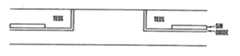
- FIG. 6illustrates a structural top view of the devices of FIG. 1 showing the source, drain, and gate regions of PFET and NFET devices having TEOS and HDP isolation regions in place.
- FIGS. 7-9illustrate cross section views of a PFET structure that is fabricated using a second manufacturing method.
- the present inventioninvolves filling isolation regions, preferably shallow trench isolation (“STI”) with different intrinsically stress inducing materials to impart selected longitudinal and transverse stress components upon active device regions formed in a substrate.
- STIshallow trench isolation
- a stress inducing material that is intrinsically tensilecauses a tensile state of stress in the substrate and an intrinsically compressive material causes compression in the substrate.
- deposited filmsthat impose different intrinsic stresses.
- TEOSTETRAETHYLORTHOSILICATE
- HDPHigh density Plasma oxide
- the key hereis to integrate two different intrinsically stress inducing structures adjacent the NFET and PFET structures or, individually, one or two stress inducing structures adjacent one of these devices.
- the process steps for integrating TEOS, which has tensile intrinsic stress, and HDP, which has compressive intrinsic stress,are shown and described below in FIGS. 3-7 and the accompanying specification.
- the present inventive methodalso includes a novel STI process flow that results in a SiN (silicon nitride) liner for both transverse and longitudinal components for NFETs but only in a transverse component for PFETs.
- This processincorporates TEOS for the STI fill because TEOS is permeable to O 2 and the SiN liner prevents oxidation from occurring at the Si/TEOS boundary. Therefore, only the longitudinal component of the PFET will be oxidized, which causes the Si/TEOS boundary to expand.
- the amount and time of oxidationcan be used to controllably increase the compressive stress for the PFET in the longitudinal direction.
- TEOSis intrinsically a tensile film and a SiN liner is used for both transverse and longitudinal components of the NFET and the transverse component of the PFET, there will be a tensile stress exerted by the TEOS STI in these directions.
- Standard STI processestypically utilize a single type of oxide film (a nitride liner is optional) for isolation together with an isolation fill material.
- a nitride lineris optional
- different types of oxide filmare selectively placed in substrate regions surrounding FET devices. By controlling the fabrication process conditions, the type of stress imparted to adjacent FET devices can also be controlled.
- NFET and PFET devicesrequire different stress vectors, or patterns, to enhance charge mobility.
- the isolation materialcan be fined tuned to produce a desired stress pattern in the device. Some materials are amenable to further fine tuning via process controls, such as RF power, for example.
- TEOSis harder to fine tune via process controls because it's a loosely structured material, but it tends to shrink when densified (annealed), thereby imparting one type of intrinsic stress—tensile.
- HDPis somewhat more controllable than TEOS, it also does not require densification (heat treatment) and typically provides intrinsic compressive stress.
- FIG. 1illustrates a preferred embodiment of the present invention.
- the outwardly directed arrows, shown extending from the NFET,illustrate a tensile stress that is induced in the transverse and longitudinal directions of the device.
- TEOScan be utilized in the present inventive method to impose these stresses in an NFET.
- TEOSis also applied, abutting or adjacent to, the transverse sides of the PFET to produce transverse tensile vectors in the PFET.
- HDPis formed adjacent the longitudinal sides of the PFET to produce longitudinal compression vectors in the PFET.
- the end structurecomprises an NFET with SiN liner on both longitudinal and transverse components, a PFET with SiN liner on transverse component, and oxidized Si with no SiN liner on the longitudinal component.
- FIG. 6The location of the HDP and the TEOS stress inducing regions, in relation to the device regions, is also shown in FIG. 6 .
- the NFETis surrounded by TEOS to produce tensile stresses in the NFET transversely and longitudinally.
- the PFET of FIG. 6illustrates TEOS fabricated on transverse sides of the PFET, to produce transverse tensile vectors, and HDP fabricated on longitudinal sides of the PFET to produce longitudinal compression vectors in the PFET. This structure results in enhanced performance for both the NFET and PFET simultaneously.
- FIG. 2illustrates the compression/tension vectors described above in cross-section views.
- the cross-section viewsillustrate the FET gates fabricated on the device substrate above the device channel regions.
- both transverse and longitudinal tensile stress in the channel substrateis shown by the outwardly pointing arrows indicating the direction of stress.
- tensile stressis indicated in the transverse direction while compressive stress (inwardly pointing arrows) is indicated in the longitudinal direction.
- the NFET and PFETcan be used together simultaneously, for example, in a ring oscillator.
- the ring oscillatorperforms ideally when beneficial aspects of the present invention in both devices are balanced, i.e. charge mobility is equivalently enhanced.
- Another structural use for the present inventionincludes formation of the silicon source and drain regions in “island” configurations, wherein a substrate device area is surrounded by dielectric STI material, or in SOI (silicon-on-insulator) devices.
- TEOS depositioninvolves a CVD (chemical vapor deposition) process.
- HDP plasma depositionis a directional process wherein the material is accelerated by an electric field because, in the plasma, HDP is composed of charged particles.
- HDPhas an intrinsic (as deposited) compressive stress and densifies as part of its deposition process.
- TEOSrequires a densification anneal after its deposition, but is intrinsically tensile.
- the substrate stressescan be imparted because of shrinking/expansion of a stress inducing material or they can be imposed intrinsically when the stress inducing material is being grown adjacent to the substrate.
- HDPhas a built-in intrinsic stress which is imparted to the substrate upon deposition (while the HDP is grown). Contraction occurs during heat treatment (densification) for TEOS.
- the underlying elemental mechanisms which induce stressesare not part of the present invention. Therefore, further theoretical details of those mechanisms will not be further addressed.
- isolation materialsselected and formed in substrate regions surrounding FET devices for isolation, are novel.
- a maskis used to open regions in the substrate.
- a unique integration schemeis used to deposit TEOS and HDP in selected portions of the wafer.
- the HDP regionsare inlaid into a TEOS background.
- the tensile components and the compressive componentsare decoupled.
- the tensile componentis established first, by varying the densification process of the TEOS. Temperature and time can vary the stress built into the TEOS, which control the amount of shrinkage (800-1050 C., 1 to 30 minutes, varying inversely). These variables determine how much the TEOS shrinks to some degree (densification). The TEOS molecules become more closely packed in densification and thereby cause tension in the adjacent Si island.
- the compression in the HDP SiO 2is controlled mostly by the deposition conditions. Tuning of the compressive stress is achieved by control of RF the power. Increased power leads to more compression in the film. Pressure and Flow can also be used to modulate the compression in the HDP SiO 2 film.
- FIG. 3illustrates formation of a silicon “island” surrounded by TEOS.
- the raised silicon areais the same for both PFETs and NFETs in both the lengthwise and widthwise cross sections.
- This raised silicon areais achieved by well known processes, which includes forming a pad layer (thin thermally oxidized pad), then depositing a SiN layer, then a mask is used to pattern openings in the SiN layer, then etching SiN, SiO 2 and finally silicon.
- a thermal oxidationwhich provides a thin oxide layer on the exposed silicon, followed by a thin conformal nitride layer deposition to protect the silicon from oxidation during TEOS anneals (densification) and other anneals during processing.
- Blanket TEOS deposition followed by chemical-mechanical planarization (“CMP”) down to the nitride liner surfaceresults in the cross-section shown in FIG. 3 .
- FIG. 4illustrates the next steps of the process which provide the HDP in selected locations for the PFET in order to impart the desired longitudinal compressive stress.
- the NFETsare covered by the resist layer in the longitudinal and transverse aspects while the PFETs are covered only in the transverse direction, leaving the PFET TEOS uncovered in the longitudinal direction.
- This exposed TEOSis removed by an etch step (upper right of FIG. 4 ).
- the resist layeris then etched from the substrate surface, followed by HDP deposition and a final CMP step over the entire surface to achieve the structure shown in cross-section in FIG. 5 , and shown in top view in FIG. 6 .
- Conventional gate formation and processing stepsfollow in the normal course.
- a second method for fabricating the structure of FIG. 1 and FIG. 2proceeds as follows, and is shown in FIGS. 7-9 . Following the same steps as in the previous process to achieve the structure shown in FIG. 3 only without the TEOS fill and CMP, another mask is then defined only for the longitudinal components of the PFET where we want to remove the nitride liner, similar to that shown in the upper right portion of FIG. 4 .
- nitride linersurrounding the silicon island (it is removed from the PFET regions where compressive stress is desired). This allows oxygen to reach the silicon sidewalls during subsequent oxidation steps, and so in this aspect the nitride liner layer acts as an oxidation blocking layer. The nitride liner would block the oxidation, and thus the compression, because it is an excellent oxygen diffusion barrier. In areas where the SiN liner is removed, a portion of the Si on the sidewall of the Si island may be oxidized, thereby causing a controlled amount of compression in the direction longitudinal to current flow for the PFET.
- the oxidationcauses a compressive stress to be generated due to volume expansion on the sidewall of the Si island.
- the oxygenwill diffuse through the TEOS oxidizing the silicon sidewall, growing a wedge of oxide and will push against the TEOS, causing the desired compression.
- a silicon trench etch with corresponding hard maskingproduces the result as shown in FIG. 1 , wherein the SiN layer is removed from the silicon island sidewalls.
- an oxide lineris grown on the exposed silicon and TEOS is deposited, followed by a CMP step down to the SiN pad, followed by a SiN pad etch, and a SiO 2 pad etch—the pad etches remove SiN and oxide from the top of the silicon island—resulting in the structure shown in FIG. 8 .
- an oxidation stepoxidizes a portion of the silicon island as shown in FIG. 9 .
- the oxidation stepis performed prior to pad nitride and oxide removal.
- Rim et. al.apply biaxial tension in strained silicon using a SiGe relaxed sub-layer.
- One of the major mechanisms by which the misfit dislocations are formedis from threading dislocations. Unfortunately, the threading dislocations can cause significant reliability, yield, and major leakage issues and are difficult to remove in practice.
- the present solutionshows how to apply the correct states of stress through modifying the STI process to benefit both the NFET and PFET simultaneously. It also differs substantially from both of these other approaches since the tension and compression are done through the STI structure and process whereas prior art listed above shows the stress is imposed through strained Si in one case and from intrinsic stress in a layer that comes well after the device build (and not adjacent the device as we do) in another.
- the advantages of the method of the preferred embodiment of this inventioninclude: device performance improvements for NFETs, PFETs, and for both NFETs and PFETs simultaneously by inducing in-plane stress patterns; a process readily integratible into present manufacturing processes for bulk silicon, silicon-on-insulator (“SOI”), and strained silicon structures; and improved devices be integrated into present processes cheaply for significant device performance improvements by adding a single mask step.
- SOIsilicon-on-insulator
- nitride filmscan be readily modulated to have very high intrinsic stress.
- the PECVD nitride etch stop film stresscould be modulated (by changing the deposition conditions such as SiH4/N 2 /He flow rates, pressure, HF power, and electrode gap) between ⁇ 1.4 GPa and +0.3 GPa.
- the deposition conditionssuch as SiH4/N 2 /He flow rates, pressure, HF power, and electrode gap
- Intrinsic stressis not the only way to add stress into this structural system.
- the magnitude of tensile stressis determined by the coefficients of thermal expansion. In the NFET tension in both dimensions (biaxial) is good, while for the PFET we would like to use this material property difference that causes tension only in the transverse direction, while still using a highly compressive intrinsic material in the longitudinal direction.
- Nonconventional devicescan also be fabricated using the present invention, such as pillar FETs and fin FETS.
- a pillar FETthe body of the device is a cylindrical shape formed in a substrate with source/drain diffusions formed at the top and bottom of the cylinder.
- the gate regiontypically is adjacent to, or surrounds, the middle portion of the cylinder.
- a fin FETcomprises a thin, elongated, raised substrate region with source and drain diffusions at the ends of the raised region.
- the gateis typically adjacent three sides of the raised region, the two vertical sides and the top surface of the raised region, between the source/drain diffusions.
- the general conceptis to inlay isolation to produce a stress pattern at least in the channel region of the devices or at least in the source/drain diffusion regions.
Landscapes
- Engineering & Computer Science (AREA)
- Physics & Mathematics (AREA)
- Condensed Matter Physics & Semiconductors (AREA)
- General Physics & Mathematics (AREA)
- Manufacturing & Machinery (AREA)
- Computer Hardware Design (AREA)
- Microelectronics & Electronic Packaging (AREA)
- Power Engineering (AREA)
- Metal-Oxide And Bipolar Metal-Oxide Semiconductor Integrated Circuits (AREA)
- Element Separation (AREA)
- Insulated Gate Type Field-Effect Transistor (AREA)
Abstract
Description
- U.S. patent application Ser. No. 10/______, entitled “Stress Inducing Spacers” filed concurrently herewith is assigned to the same assignee hereof and contains subject matter related, in certain respect, to the subject matter of the present application. The above-identified patent application is incorporated herein by reference.
- 1. Technical Field of the Invention
- This invention pertains to inventive methods of manufacturing a semiconductor device for improving device performance, and to the resulting unique high-performance device structure. In particular, this invention has improved charge mobility in FET devices by structurally imposing tensile and compression forces in a device substrate during device fabrication.
- Within the field of semiconductor device design, it is known that mechanical stresses within the device substrate can modulate device performance. Individual stress tensor components affect device behavior of PFETs and NFETs differently. Previous improvements that utilized stress enhancements tended to focus on one or the other type of device outside of a practical performance environment, such as in an IC chip. In order to maximize the performance of both PFETs and NFETs within IC chips, the stress components need to be engineered and applied differently, yet simultaneously. In the present invention we show fabrication methods and resulting structures that have imposed the appropriate stress fields needed to improve the performance of a single device and of at least two devices simultaneously in a common substrate.
- 2. Description of the Prior Art
- Hamada et al, IEEE Transactions on Electron Devices, Vol. 38 No. 4,A New Aspect of Mechanical Stress Effects in Scaled MOS Devices(April 1991) show data correlating weight induced (bending a sample silicon chip) longitudinal and transverse tensile and compressive stress with Transconductance deviation. Within the PFET device a longitudinally applied uniaxial compressive stress had an effect reversed from the effect induced on an NFET. This data can be interpreted such that if you apply an in-plane biaxial tensile stress, the NFET device performance will improve about two-fold as compared to that of a uniaxial tensile situation, while the PFET experiences no change because the longitudinal and transverse tensile stress effects cancel each other out.
- In the Symposium on VLSI Technology Digest of Technical Papers (2001), Rim et. al. shows that, using strained Si which has in-plane biaxial tensile stress, improvements occurred for an NFET with a 70% increase in electron mobility. Prior known solutions and methods using mechanical stress for device performance enhancement could not improve both NFETs and PFETs simultaneously. Moreover, prior solutions do not address the feasibility of any kind of device structures or methods of fabricating them.
- In this invention we show methods and structures by which we have applied in-plane biaxial (two-dimensional) tensile stress for the NFET while at the same time applying in-plane compressive longitudinal stress and a tensile transverse stress on the PFET device. The structures and methods of making each device individually is also unique. The primary advantage of these methods and structures is that they have provided two-fold device performance improvement relative to merely uniaxial stresses. Another advantage is the method for fabricating NFETs and PFETs simultaneously on a common substrate, wherein each device is designed to enhance performance using stress inducing isolation material. A secondary advantage is the structure and method of building an individual device with enhanced performance provided via stress inducing trench isolation structures.
- It is an object of the present invention to provide device performance improvements for NFETs, PFETs, and for both NFETs and PFETs simultaneously. It is another object of the present invention to be readily integratible into present manufacturing processes cheaply for significant device performance improvements by adding a single mask step. It is another object of the present invention to be manufacturable in bulk silicon, silicon-on-insulator (“SOI”), and strained silicon structures.
- This invention comprises a trench isolation structure for an NFET device and for a PFET device. An isolation region for the NFET device contains therein a first isolation material which applies a first type of mechanical stress on the NFET device in a longitudinal direction and in a transverse direction. A first isolation region for the PFET device applies mechanical stress on the PFET device in the transverse direction. A second isolation region for the PFET device applies another type of mechanical stress on the PFET device in the longitudinal direction. The isolation regions may comprise similar or different isolation materials depending upon which type of mechanical stress is desired. Typically, the mechanical stresses are either tensile or compressive.
- In another aspect, this invention comprises a method for making NFET and PFET devices. This aspect incorporates the formation of isolation regions at the sides and at the ends of the NFET device. Another isolation region is formed at the sides of the PFET device. Another (third) trench isolation region is formed at the ends of the PFET device. Isolation materials in these isolation regions are selected to apply a first type of mechanical stress on the NFET device both in a longitudinal direction and in a transverse direction, and on the PFET device in the transverse direction. Isolation material in the third trench isolation region can be selected to apply a compressive type of mechanical stress in the longitudinal direction of the PFET. In another method of inducing stress vectors, it is useful to oxidize, in order to expand, at least a portion of the isolation material in the third trench isolation region to apply the compressive mechanical stress on the PFET device in the longitudinal direction. Thus, the isolation materials selected may be the same or different for each device depending on whether oxidation is used to induce stress components.
- In another aspect, the present invention comprises source and drain regions formed in a substrate. The substrate having a channel region between each of the source and drain regions. A gate region adjacent the channel region controls conduction through the channel region. Stress inducing isolation material adjacent selected sides of the source and drain regions imparts stress, i.e. tension or compression, beyond the source and drain regions of the substrate at least into the channel region.
- Other features and advantages of this invention will become apparent from the following detailed description of the presently preferred embodiment of the invention, taken in conjunction with the accompanying drawings.
FIG. 1 illustrates desired stress states that improve performance of PFETs and NFETs, wherein the outward arrows from the device active area illustrate tension, and inward arrows toward the device area illustrate compression, and W and L illustrate width and length of the active area of the device, respectively.FIG. 2 illustrates cross section views of the devices ofFIG. 1 along length and width planes.FIGS. 3-5 illustrate process steps for fabricating stressed NFET and PFET structures.FIG. 6 illustrates a structural top view of the devices ofFIG. 1 showing the source, drain, and gate regions of PFET and NFET devices having TEOS and HDP isolation regions in place.FIGS. 7-9 illustrate cross section views of a PFET structure that is fabricated using a second manufacturing method.- The present invention involves filling isolation regions, preferably shallow trench isolation (“STI”) with different intrinsically stress inducing materials to impart selected longitudinal and transverse stress components upon active device regions formed in a substrate. For example, using a stress inducing material that is intrinsically tensile causes a tensile state of stress in the substrate and an intrinsically compressive material causes compression in the substrate. In order to impart these different stresses in devices, we use deposited films that impose different intrinsic stresses. For example, TEOS (TETRAETHYLORTHOSILICATE) is known to be tensile because it undergoes densification under anneal and so it shrinks, thereby imposing upon an adjacent substrate a tensile stress. HDP (High density Plasma) oxide is known to be intrinsically compressive. The key here is to integrate two different intrinsically stress inducing structures adjacent the NFET and PFET structures or, individually, one or two stress inducing structures adjacent one of these devices. The process steps for integrating TEOS, which has tensile intrinsic stress, and HDP, which has compressive intrinsic stress, are shown and described below in
FIGS. 3-7 and the accompanying specification. - The present inventive method also includes a novel STI process flow that results in a SiN (silicon nitride) liner for both transverse and longitudinal components for NFETs but only in a transverse component for PFETs. This process incorporates TEOS for the STI fill because TEOS is permeable to O2and the SiN liner prevents oxidation from occurring at the Si/TEOS boundary. Therefore, only the longitudinal component of the PFET will be oxidized, which causes the Si/TEOS boundary to expand. The amount and time of oxidation can be used to controllably increase the compressive stress for the PFET in the longitudinal direction. Also, since TEOS is intrinsically a tensile film and a SiN liner is used for both transverse and longitudinal components of the NFET and the transverse component of the PFET, there will be a tensile stress exerted by the TEOS STI in these directions.
- Standard STI processes typically utilize a single type of oxide film (a nitride liner is optional) for isolation together with an isolation fill material. In the present invention, different types of oxide film are selectively placed in substrate regions surrounding FET devices. By controlling the fabrication process conditions, the type of stress imparted to adjacent FET devices can also be controlled.
- NFET and PFET devices require different stress vectors, or patterns, to enhance charge mobility. The isolation material can be fined tuned to produce a desired stress pattern in the device. Some materials are amenable to further fine tuning via process controls, such as RF power, for example. TEOS is harder to fine tune via process controls because it's a loosely structured material, but it tends to shrink when densified (annealed), thereby imparting one type of intrinsic stress—tensile. HDP is somewhat more controllable than TEOS, it also does not require densification (heat treatment) and typically provides intrinsic compressive stress.
FIG. 1 illustrates a preferred embodiment of the present invention. The outwardly directed arrows, shown extending from the NFET, illustrate a tensile stress that is induced in the transverse and longitudinal directions of the device. As will be further described, TEOS can be utilized in the present inventive method to impose these stresses in an NFET. TEOS is also applied, abutting or adjacent to, the transverse sides of the PFET to produce transverse tensile vectors in the PFET. HDP is formed adjacent the longitudinal sides of the PFET to produce longitudinal compression vectors in the PFET.- In another embodiment, the end structure comprises an NFET with SiN liner on both longitudinal and transverse components, a PFET with SiN liner on transverse component, and oxidized Si with no SiN liner on the longitudinal component. Several process flows are possible to arrive at the final structure.
- The location of the HDP and the TEOS stress inducing regions, in relation to the device regions, is also shown in
FIG. 6 . InFIG. 6 , the NFET is surrounded by TEOS to produce tensile stresses in the NFET transversely and longitudinally. The PFET ofFIG. 6 illustrates TEOS fabricated on transverse sides of the PFET, to produce transverse tensile vectors, and HDP fabricated on longitudinal sides of the PFET to produce longitudinal compression vectors in the PFET. This structure results in enhanced performance for both the NFET and PFET simultaneously. FIG. 2 illustrates the compression/tension vectors described above in cross-section views. The cross-section views illustrate the FET gates fabricated on the device substrate above the device channel regions. In the NFET, both transverse and longitudinal tensile stress in the channel substrate is shown by the outwardly pointing arrows indicating the direction of stress. In the PFET, tensile stress is indicated in the transverse direction while compressive stress (inwardly pointing arrows) is indicated in the longitudinal direction. Taken together, the preceding figures clearly illustrate the tensile and compressive forces in the FET devices in all three dimensions.- In the simultaneous PFET/NFET embodiment of the present invention, the NFET and PFET can be used together simultaneously, for example, in a ring oscillator. The ring oscillator performs ideally when beneficial aspects of the present invention in both devices are balanced, i.e. charge mobility is equivalently enhanced. Another structural use for the present invention includes formation of the silicon source and drain regions in “island” configurations, wherein a substrate device area is surrounded by dielectric STI material, or in SOI (silicon-on-insulator) devices.
- The two preferred trench isolation materials, HDP and TEOS, differ in several aspects. The deposition processes of TEOS and HDP are different: TEOS deposition involves a CVD (chemical vapor deposition) process. HDP plasma deposition is a directional process wherein the material is accelerated by an electric field because, in the plasma, HDP is composed of charged particles. HDP has an intrinsic (as deposited) compressive stress and densifies as part of its deposition process. TEOS requires a densification anneal after its deposition, but is intrinsically tensile.
- The substrate stresses can be imparted because of shrinking/expansion of a stress inducing material or they can be imposed intrinsically when the stress inducing material is being grown adjacent to the substrate. HDP has a built-in intrinsic stress which is imparted to the substrate upon deposition (while the HDP is grown). Contraction occurs during heat treatment (densification) for TEOS. The underlying elemental mechanisms which induce stresses are not part of the present invention. Therefore, further theoretical details of those mechanisms will not be further addressed.
- The structure and choice of isolation materials, selected and formed in substrate regions surrounding FET devices for isolation, are novel. Generally speaking, a mask is used to open regions in the substrate. Next, a unique integration scheme is used to deposit TEOS and HDP in selected portions of the wafer. In one of several embodiments, the HDP regions are inlaid into a TEOS background.
- The tensile components and the compressive components are decoupled. The tensile component is established first, by varying the densification process of the TEOS. Temperature and time can vary the stress built into the TEOS, which control the amount of shrinkage (800-1050 C., 1 to 30 minutes, varying inversely). These variables determine how much the TEOS shrinks to some degree (densification). The TEOS molecules become more closely packed in densification and thereby cause tension in the adjacent Si island. The compression in the HDP SiO2, is controlled mostly by the deposition conditions. Tuning of the compressive stress is achieved by control of RF the power. Increased power leads to more compression in the film. Pressure and Flow can also be used to modulate the compression in the HDP SiO2film.
- The process for fabricating NFETs and PFETs with different stresses in the channel region, on a common substrate is illustrated in
FIGS. 3-5 and is described as follows.FIG. 3 illustrates formation of a silicon “island” surrounded by TEOS. The raised silicon area is the same for both PFETs and NFETs in both the lengthwise and widthwise cross sections. This raised silicon area is achieved by well known processes, which includes forming a pad layer (thin thermally oxidized pad), then depositing a SiN layer, then a mask is used to pattern openings in the SiN layer, then etching SiN, SiO2and finally silicon. After the mask is removed, a thermal oxidation, which provides a thin oxide layer on the exposed silicon, followed by a thin conformal nitride layer deposition to protect the silicon from oxidation during TEOS anneals (densification) and other anneals during processing. Blanket TEOS deposition followed by chemical-mechanical planarization (“CMP”) down to the nitride liner surface results in the cross-section shown inFIG. 3 . - Up to this point, the present inventive process follows conventional process steps.
FIG. 4 illustrates the next steps of the process which provide the HDP in selected locations for the PFET in order to impart the desired longitudinal compressive stress. Using standard masking techniques, the NFETs are covered by the resist layer in the longitudinal and transverse aspects while the PFETs are covered only in the transverse direction, leaving the PFET TEOS uncovered in the longitudinal direction. This exposed TEOS is removed by an etch step (upper right ofFIG. 4 ). This is the single masking step added by the present invention over conventional processes. The resist layer is then etched from the substrate surface, followed by HDP deposition and a final CMP step over the entire surface to achieve the structure shown in cross-section inFIG. 5 , and shown in top view inFIG. 6 . Conventional gate formation and processing steps follow in the normal course. - A second method for fabricating the structure of
FIG. 1 andFIG. 2 proceeds as follows, and is shown inFIGS. 7-9 . Following the same steps as in the previous process to achieve the structure shown inFIG. 3 only without the TEOS fill and CMP, another mask is then defined only for the longitudinal components of the PFET where we want to remove the nitride liner, similar to that shown in the upper right portion ofFIG. 4 . - Because we want to induce longitudinal compressive stress in the PFET, we remove the nitride liner surrounding the silicon island (it is removed from the PFET regions where compressive stress is desired). This allows oxygen to reach the silicon sidewalls during subsequent oxidation steps, and so in this aspect the nitride liner layer acts as an oxidation blocking layer. The nitride liner would block the oxidation, and thus the compression, because it is an excellent oxygen diffusion barrier. In areas where the SiN liner is removed, a portion of the Si on the sidewall of the Si island may be oxidized, thereby causing a controlled amount of compression in the direction longitudinal to current flow for the PFET. Good control in the oxide sidewall growth may be achieved using this method, because you can dial in the amount of compression achieved because of the amount of oxide grown, instead of relying on the HDP deposition conditions. The oxidation causes a compressive stress to be generated due to volume expansion on the sidewall of the Si island. The oxygen will diffuse through the TEOS oxidizing the silicon sidewall, growing a wedge of oxide and will push against the TEOS, causing the desired compression.
- At this point, a silicon trench etch with corresponding hard masking produces the result as shown in
FIG. 1 , wherein the SiN layer is removed from the silicon island sidewalls. Next, an oxide liner is grown on the exposed silicon and TEOS is deposited, followed by a CMP step down to the SiN pad, followed by a SiN pad etch, and a SiO2pad etch—the pad etches remove SiN and oxide from the top of the silicon island—resulting in the structure shown inFIG. 8 . Then, an oxidation step oxidizes a portion of the silicon island as shown inFIG. 9 . In an alternate approach, the oxidation step is performed prior to pad nitride and oxide removal. It is known that when Si is transformed into SiO2, a volume expansion of approximately 2.27:1 occurs. The oxidized material narrows with depth because as the oxygen diffuses downward, the concentration drops off due to oxygen consumption during the oxidation step. Thus, the oxygen concentration is higher at the top and it grows slightly thicker in the near surface region forming a wedge shape. The longer the oxidation, the wider the wedge. The idea is that the volume is expanded and compressive force pushes on the silicon inwardly. Conventional gate formation and processing follows and is not described further. It is to be noted that the device regions and isolation regions in these figures are not drawn to scale in any dimension. - The benefit of using this scheme for achieving tension in the NFET and transverse component for PFET and compressive stress in the longitudinal component for the PFET is that the oxidation time and temperature can be used to tune the stress for the longitudinal component for the PFET.
- In the prior art, Rim et. al. apply biaxial tension in strained silicon using a SiGe relaxed sub-layer. The problems there are many. While the NFET shows what may be considered significant improvement, they could not simultaneously improve both devices. Also, since the requirement is a relaxed SiGe layer, misfit dislocations are needed at the SiGe/Si interface. One of the major mechanisms by which the misfit dislocations are formed is from threading dislocations. Unfortunately, the threading dislocations can cause significant reliability, yield, and major leakage issues and are difficult to remove in practice.
- Mechanical Stress Effect of Etch-Stop Nitride and its Impact on Deep Submicron Transistor Design,Ito et al (IEDM, 2000) impose stress using an etch-stop nitride superlayer that is deposited after the device is completely constructed. Again, here the films have a built-in intrinsic biaxial stress. They found that when the film is in compression NFET performance is degraded, while the PFET is enhanced. Also, they did not improve the performance of both the PFET and NFET simultaneously. Also, since the film is well above the device the stress translated down into the silicon will be somewhat lessened, particularly when compared to something that is directly adjacent the device.
- The present solution shows how to apply the correct states of stress through modifying the STI process to benefit both the NFET and PFET simultaneously. It also differs substantially from both of these other approaches since the tension and compression are done through the STI structure and process whereas prior art listed above shows the stress is imposed through strained Si in one case and from intrinsic stress in a layer that comes well after the device build (and not adjacent the device as we do) in another.
- The advantages of the method of the preferred embodiment of this invention include: device performance improvements for NFETs, PFETs, and for both NFETs and PFETs simultaneously by inducing in-plane stress patterns; a process readily integratible into present manufacturing processes for bulk silicon, silicon-on-insulator (“SOI”), and strained silicon structures; and improved devices be integrated into present processes cheaply for significant device performance improvements by adding a single mask step.
- It will be appreciated that, although specific embodiments of the invention have been described herein for purposes of illustration, various modifications may be made without departing from the spirit and scope of the invention. In particular, other isolation materials can be used, such as ceramics and silicon carbide, which can also impart intrinsic stresses. The general view of stresses in silicon is that it's disadvantageous. Stresses lead to ruptures or dislocations in the lattice structure, which lead to junction leakage, etc. In the present invention, we're intentionally building in a stress pattern.
- As another example, nitride films can be readily modulated to have very high intrinsic stress. For example, as shown in Ito et al (IEDM, 2000) the PECVD nitride etch stop film stress could be modulated (by changing the deposition conditions such as SiH4/N2/He flow rates, pressure, HF power, and electrode gap) between −1.4 GPa and +0.3 GPa. Of course, since nitride films have a higher dielectric constant, they will need deeper STI with perhaps larger isolation distances between devices. Hu (JAP, 1991) provides a partial listing of intrinsic stresses in some films. One could use a combination of highly intrinsic stressed films as part of the STI. This adds complexity, but allows for perhaps better tailoring of the stress.
- Intrinsic stress is not the only way to add stress into this structural system. By choosing the correct materials with the appropriate thermal expansion coefficient mismatch, we can modulate the tensile stress. Since cool down is when the stress is imposed (operating conditions are between 25 C. and 85 C.), the net thermal mismatch stress will always be tensile. The magnitude of tensile stress is determined by the coefficients of thermal expansion. In the NFET tension in both dimensions (biaxial) is good, while for the PFET we would like to use this material property difference that causes tension only in the transverse direction, while still using a highly compressive intrinsic material in the longitudinal direction.
- Nonconventional devices can also be fabricated using the present invention, such as pillar FETs and fin FETS. In a pillar FET, the body of the device is a cylindrical shape formed in a substrate with source/drain diffusions formed at the top and bottom of the cylinder. The gate region typically is adjacent to, or surrounds, the middle portion of the cylinder. A fin FET comprises a thin, elongated, raised substrate region with source and drain diffusions at the ends of the raised region. The gate is typically adjacent three sides of the raised region, the two vertical sides and the top surface of the raised region, between the source/drain diffusions. The general concept is to inlay isolation to produce a stress pattern at least in the channel region of the devices or at least in the source/drain diffusion regions. The appended claims are intended not to exclude various device geometries such as pillar FETs and fin FETs. Providing a uniform background of TEOS fill, then selectively opening regions for HDP deposition is a process that can accommodate device geometries other than those specifically illustrated in the present specification as preferred, currently known embodiments.
- Accordingly, the scope of protection of this invention is limited only by the following claims and their equivalents.
Claims (9)
1-8. (canceled)
9. A method for making devices in a substrate, the devices each having sides extending in a longitudinal direction and ends extending in a transverse direction, the method comprising:
forming a first isolation region at the sides and at the ends of a first one of the devices;
providing a first isolation material in the first isolation region to apply a first type of mechanical stress on the first one of the devices in the transverse direction; and
oxidizing at least a portion of the first isolation material at the ends of the first one of the devices to cause the first isolation material to apply a second type of mechanical stress on the first one of the devices in the longitudinal direction.
10. The method ofclaim 9 , further comprising:
forming a second isolation region at the sides and at the ends of a second one of the devices; and
providing the first isolation material in the second isolation region to apply the first type of mechanical stress on the second one of the devices in the longitudinal direction and also in the transverse direction.
11. The method ofclaim 10 , wherein the step of forming a first isolation region comprises:
depositing an oxidation blocking layer over the first and second ones of the devices; and
removing the oxidation blocking layer only from over the ends of the first one of the devices.
12. The method ofclaim 10 , wherein the step of oxidizing at least a portion of the first isolation material comprises:
simultaneously oxidizing at least a portion of the ends of the first one of the devices.
13. The method ofclaim 10 , wherein the first one of the devices is a PFET and the second one of the devices is an NFET.
14. An isolation structure for devices formed in a substrate, the devices each having sides extending in a longitudinal direction and ends extending in a transverse direction, the structure comprising:
a first isolation region adjacent at least one side and at least one end of a first one of the devices, the first isolation region having therein a first isolation material, the first isolation material adjacent said at least one side of the first one of the devices for applying a first type of mechanical stress on the first one of the devices in the transverse direction; and
an oxidized portion of the first isolation material adjacent said at least one end of the first one of the devices for applying a second type of mechanical stress on the first one of the devices in the longitudinal direction.
15. The isolation structure ofclaim 14 , further comprising:
a second isolation region for a second one of the devices, the second isolation region having therein the first isolation material which applies the first type of mechanical stress on the second one of the devices in the longitudinal direction and also in the transverse direction.
16. The isolation structure ofclaim 15 , wherein the first one of the devices is a PFET and the second one of the devices is an NFET.
Priority Applications (1)
| Application Number | Priority Date | Filing Date | Title |
|---|---|---|---|
| US11/200,958US20050280051A1 (en) | 2002-12-12 | 2005-08-10 | Isolation structures for imposing stress patterns |
Applications Claiming Priority (2)
| Application Number | Priority Date | Filing Date | Title |
|---|---|---|---|
| US10/318,600US6974981B2 (en) | 2002-12-12 | 2002-12-12 | Isolation structures for imposing stress patterns |
| US11/200,958US20050280051A1 (en) | 2002-12-12 | 2005-08-10 | Isolation structures for imposing stress patterns |
Related Parent Applications (1)
| Application Number | Title | Priority Date | Filing Date |
|---|---|---|---|
| US10/318,600DivisionUS6974981B2 (en) | 2002-12-12 | 2002-12-12 | Isolation structures for imposing stress patterns |
Publications (1)
| Publication Number | Publication Date |
|---|---|
| US20050280051A1true US20050280051A1 (en) | 2005-12-22 |
Family
ID=32506402
Family Applications (2)
| Application Number | Title | Priority Date | Filing Date |
|---|---|---|---|
| US10/318,600Expired - LifetimeUS6974981B2 (en) | 2002-12-12 | 2002-12-12 | Isolation structures for imposing stress patterns |
| US11/200,958AbandonedUS20050280051A1 (en) | 2002-12-12 | 2005-08-10 | Isolation structures for imposing stress patterns |
Family Applications Before (1)
| Application Number | Title | Priority Date | Filing Date |
|---|---|---|---|
| US10/318,600Expired - LifetimeUS6974981B2 (en) | 2002-12-12 | 2002-12-12 | Isolation structures for imposing stress patterns |
Country Status (3)
| Country | Link |
|---|---|
| US (2) | US6974981B2 (en) |
| CN (1) | CN1270370C (en) |
| TW (1) | TWI230433B (en) |
Cited By (50)
| Publication number | Priority date | Publication date | Assignee | Title |
|---|---|---|---|---|
| US20050054145A1 (en)* | 2003-09-09 | 2005-03-10 | International Business Machines Corporation | Method for reduced n+ diffusion in strained si on sige substrate |
| US20050082634A1 (en)* | 2003-10-16 | 2005-04-21 | International Business Machines Corporation | High performance strained cmos devices |
| US20050158955A1 (en)* | 2004-01-16 | 2005-07-21 | International Business Machines Corporation | Method and apparatus to increase strain effect in a transistor channel |
| US20060163608A1 (en)* | 2004-01-16 | 2006-07-27 | International Business Machines Corporation | Protecting silicon germanium sidewall with silicon for strained silicon silicon mosfets |
| US20060220142A1 (en)* | 2005-03-31 | 2006-10-05 | Fujitsu Limited | Semiconductor device and manufacturing method thereof |
| US20060228867A1 (en)* | 2005-04-12 | 2006-10-12 | Taxas Instruments Incorporated | Isolation region formation that controllably induces stress in active regions |
| US7122849B2 (en) | 2003-11-14 | 2006-10-17 | International Business Machines Corporation | Stressed semiconductor device structures having granular semiconductor material |
| US7129126B2 (en) | 2003-11-05 | 2006-10-31 | International Business Machines Corporation | Method and structure for forming strained Si for CMOS devices |
| US7144767B2 (en) | 2003-09-23 | 2006-12-05 | International Business Machines Corporation | NFETs using gate induced stress modulation |
| US7198995B2 (en) | 2003-12-12 | 2007-04-03 | International Business Machines Corporation | Strained finFETs and method of manufacture |
| US7205206B2 (en) | 2004-03-03 | 2007-04-17 | International Business Machines Corporation | Method of fabricating mobility enhanced CMOS devices |
| US7223994B2 (en) | 2004-06-03 | 2007-05-29 | International Business Machines Corporation | Strained Si on multiple materials for bulk or SOI substrates |
| US7247534B2 (en) | 2003-11-19 | 2007-07-24 | International Business Machines Corporation | Silicon device on Si:C-OI and SGOI and method of manufacture |
| US7247912B2 (en) | 2004-01-05 | 2007-07-24 | International Business Machines Corporation | Structures and methods for making strained MOSFETs |
| US7256081B2 (en) | 2005-02-01 | 2007-08-14 | International Business Machines Corporation | Structure and method to induce strain in a semiconductor device channel with stressed film under the gate |
| US7285826B2 (en) | 2003-11-06 | 2007-10-23 | International Business Machines Corporation | High mobility CMOS circuits |
| US7288443B2 (en) | 2004-06-29 | 2007-10-30 | International Business Machines Corporation | Structures and methods for manufacturing p-type MOSFET with graded embedded silicon-germanium source-drain and/or extension |
| US7303949B2 (en) | 2003-10-20 | 2007-12-04 | International Business Machines Corporation | High performance stress-enhanced MOSFETs using Si:C and SiGe epitaxial source/drain and method of manufacture |
| US7314802B2 (en) | 2005-02-15 | 2008-01-01 | International Business Machines Corporation | Structure and method for manufacturing strained FINFET |
| US7314789B2 (en) | 2004-12-15 | 2008-01-01 | International Business Machines Corporation | Structure and method to generate local mechanical gate stress for MOSFET channel mobility modification |
| US7381609B2 (en) | 2004-01-16 | 2008-06-03 | International Business Machines Corporation | Method and structure for controlling stress in a transistor channel |
| US7384829B2 (en) | 2004-07-23 | 2008-06-10 | International Business Machines Corporation | Patterned strained semiconductor substrate and device |
| US20080171426A1 (en)* | 2007-01-12 | 2008-07-17 | International Business Machines Corporation | Uniaxial strain relaxation of biaxial-strained thin films using ion implantation |
| US7462522B2 (en) | 2006-08-30 | 2008-12-09 | International Business Machines Corporation | Method and structure for improving device performance variation in dual stress liner technology |
| US7468538B2 (en) | 2003-11-13 | 2008-12-23 | International Business Machines Corporation | Strained silicon on a SiGe on SOI substrate |
| US20090032840A1 (en)* | 2007-07-31 | 2009-02-05 | International Business Machines Corporation | Semiconductor device and method of manufacture |
| US7491623B2 (en) | 2006-08-30 | 2009-02-17 | International Business Machines Corporation | Method of making a semiconductor structure |
| US7495291B2 (en) | 2003-10-20 | 2009-02-24 | International Business Machines Corporation | Strained dislocation-free channels for CMOS and method of manufacture |
| US7521307B2 (en) | 2006-04-28 | 2009-04-21 | International Business Machines Corporation | CMOS structures and methods using self-aligned dual stressed layers |
| US20090127626A1 (en)* | 2007-11-15 | 2009-05-21 | International Business Machines Corporation | Stress-generating shallow trench isolation structure having dual composition |
| US7545004B2 (en) | 2005-04-12 | 2009-06-09 | International Business Machines Corporation | Method and structure for forming strained devices |
| US7608489B2 (en) | 2006-04-28 | 2009-10-27 | International Business Machines Corporation | High performance stress-enhance MOSFET and method of manufacture |
| US7615418B2 (en) | 2006-04-28 | 2009-11-10 | International Business Machines Corporation | High performance stress-enhance MOSFET and method of manufacture |
| US20090311855A1 (en)* | 2007-10-19 | 2009-12-17 | Bruff Richard A | Method of fabricating a gate structure |
| US7691698B2 (en) | 2006-02-21 | 2010-04-06 | International Business Machines Corporation | Pseudomorphic Si/SiGe/Si body device with embedded SiGe source/drain |
| US7745277B2 (en) | 2003-09-12 | 2010-06-29 | International Business Machines Corporation | MOSFET performance improvement using deformation in SOI structure |
| US7790540B2 (en) | 2006-08-25 | 2010-09-07 | International Business Machines Corporation | Structure and method to use low k stress liner to reduce parasitic capacitance |
| US7935993B2 (en) | 2006-01-10 | 2011-05-03 | International Business Machines Corporation | Semiconductor device structure having enhanced performance FET device |
| US7960801B2 (en) | 2005-11-03 | 2011-06-14 | International Business Machines Corporation | Gate electrode stress control for finFET performance enhancement description |
| US7964865B2 (en) | 2003-09-23 | 2011-06-21 | International Business Machines Corporation | Strained silicon on relaxed sige film with uniform misfit dislocation density |
| US20110198696A1 (en)* | 2010-02-18 | 2011-08-18 | Globalfoundries Inc. | Finned semiconductor device with oxygen diffusion barrier regions, and related fabrication methods |
| US8058157B2 (en) | 2005-11-30 | 2011-11-15 | International Business Machines Corporation | FinFET structure with multiply stressed gate electrode |
| US8115254B2 (en) | 2007-09-25 | 2012-02-14 | International Business Machines Corporation | Semiconductor-on-insulator structures including a trench containing an insulator stressor plug and method of fabricating same |
| US20120168881A1 (en)* | 2010-12-29 | 2012-07-05 | Haizhou Yin | Semiconductor device and method for manufacturing the same |
| US8598006B2 (en) | 2010-03-16 | 2013-12-03 | International Business Machines Corporation | Strain preserving ion implantation methods |
| US8846488B2 (en) | 2011-10-14 | 2014-09-30 | Institute of Microelectronics, Chinese Academy of Sciences | Semiconductor device and method for manufacturing the same |
| US8853746B2 (en) | 2006-06-29 | 2014-10-07 | International Business Machines Corporation | CMOS devices with stressed channel regions, and methods for fabricating the same |
| US20140346607A1 (en)* | 2013-05-23 | 2014-11-27 | Taiwan Semiconductor Manufacturing Company, Ltd. | Tuning Tensile Strain on FinFET |
| US9472621B1 (en)* | 2015-06-29 | 2016-10-18 | International Business Machines Corporation | CMOS structures with selective tensile strained NFET fins and relaxed PFET fins |
| US20170207320A1 (en)* | 2016-01-19 | 2017-07-20 | Commissariat A L'energie Atomique Et Aux Energies Alternatives | Consumption of the channel of a transistor by sacrificial oxidation |
Families Citing this family (52)
| Publication number | Priority date | Publication date | Assignee | Title |
|---|---|---|---|---|
| US6995053B2 (en)* | 2004-04-23 | 2006-02-07 | Sharp Laboratories Of America, Inc. | Vertical thin film transistor |
| US6924543B2 (en)* | 2003-06-16 | 2005-08-02 | Intel Corporation | Method for making a semiconductor device having increased carrier mobility |
| US8008724B2 (en)* | 2003-10-30 | 2011-08-30 | International Business Machines Corporation | Structure and method to enhance both nFET and pFET performance using different kinds of stressed layers |
| TWI463526B (en)* | 2004-06-24 | 2014-12-01 | Ibm | Method for improving stress-induced CMOS components and components prepared by the method |
| JP4994581B2 (en)* | 2004-06-29 | 2012-08-08 | 富士通セミコンダクター株式会社 | Semiconductor device |
| US8669145B2 (en) | 2004-06-30 | 2014-03-11 | International Business Machines Corporation | Method and structure for strained FinFET devices |
| KR100541656B1 (en)* | 2004-08-03 | 2006-01-11 | 삼성전자주식회사 | Cmos device with improved performance and fabrication method thereof |
| US7268399B2 (en)* | 2004-08-31 | 2007-09-11 | Texas Instruments Incorporated | Enhanced PMOS via transverse stress |
| US7078722B2 (en)* | 2004-09-20 | 2006-07-18 | International Business Machines Corporation | NFET and PFET devices and methods of fabricating same |
| US7348635B2 (en)* | 2004-12-10 | 2008-03-25 | International Business Machines Corporation | Device having enhanced stress state and related methods |
| US7274084B2 (en)* | 2005-01-12 | 2007-09-25 | International Business Machines Corporation | Enhanced PFET using shear stress |
| US7358551B2 (en)* | 2005-07-21 | 2008-04-15 | International Business Machines Corporation | Structure and method for improved stress and yield in pFETs with embedded SiGe source/drain regions |
| TW200713455A (en)* | 2005-09-20 | 2007-04-01 | Applied Materials Inc | Method to form a device on a SOI substrate |
| US7221024B1 (en)* | 2005-10-27 | 2007-05-22 | International Business Machines Corporation | Transistor having dielectric stressor elements for applying in-plane shear stress |
| US7759739B2 (en)* | 2005-10-27 | 2010-07-20 | International Business Machines Corporation | Transistor with dielectric stressor elements |
| US7785950B2 (en)* | 2005-11-10 | 2010-08-31 | International Business Machines Corporation | Dual stress memory technique method and related structure |
| US7348638B2 (en)* | 2005-11-14 | 2008-03-25 | International Business Machines Corporation | Rotational shear stress for charge carrier mobility modification |
| US7476938B2 (en)* | 2005-11-21 | 2009-01-13 | International Business Machines Corporation | Transistor having dielectric stressor elements at different depths from a semiconductor surface for applying shear stress |
| US7659581B2 (en)* | 2005-11-30 | 2010-02-09 | International Business Machines Corporation | Transistor with dielectric stressor element fully underlying the active semiconductor region |
| US7678662B2 (en)* | 2005-12-13 | 2010-03-16 | Applied Materials, Inc. | Memory cell having stressed layers |
| US20070158743A1 (en)* | 2006-01-11 | 2007-07-12 | International Business Machines Corporation | Thin silicon single diffusion field effect transistor for enhanced drive performance with stress film liners |
| CN101009327B (en)* | 2006-01-23 | 2010-05-12 | 旺宏电子股份有限公司 | Semiconductor device and method for manufacturing the same |
| US7544584B2 (en) | 2006-02-16 | 2009-06-09 | Micron Technology, Inc. | Localized compressive strained semiconductor |
| US7462916B2 (en)* | 2006-07-19 | 2008-12-09 | International Business Machines Corporation | Semiconductor devices having torsional stresses |
| US7485544B2 (en)* | 2006-08-02 | 2009-02-03 | Micron Technology, Inc. | Strained semiconductor, devices and systems and methods of formation |
| US7968960B2 (en) | 2006-08-18 | 2011-06-28 | Micron Technology, Inc. | Methods of forming strained semiconductor channels |
| DE102006046377A1 (en)* | 2006-09-29 | 2008-04-03 | Advanced Micro Devices, Inc., Sunnyvale | Semiconductor device e.g. integrated circuit, has active semiconductor regions with peripheries formed by isolation trenches with dielectric filling materials, respectively, where filling materials are comprised of silicon nitride |
| WO2008042144A2 (en)* | 2006-09-29 | 2008-04-10 | Advanced Micro Devices, Inc. | A semiconductor device comprising isolation trenches inducing different types of strain |
| US20080142897A1 (en)* | 2006-12-19 | 2008-06-19 | Chartered Semiconductor Manufacturing Ltd. | Integrated circuit system having strained transistor |
| US7521763B2 (en)* | 2007-01-03 | 2009-04-21 | International Business Machines Corporation | Dual stress STI |
| US20080173950A1 (en)* | 2007-01-18 | 2008-07-24 | International Business Machines Corporation | Structure and Method of Fabricating Electrical Structure Having Improved Charge Mobility |
| US7935588B2 (en)* | 2007-03-06 | 2011-05-03 | International Business Machines Corporation | Enhanced transistor performance by non-conformal stressed layers |
| US7678665B2 (en)* | 2007-03-07 | 2010-03-16 | Freescale Semiconductor, Inc. | Deep STI trench and SOI undercut enabling STI oxide stressor |
| JP2008262954A (en)* | 2007-04-10 | 2008-10-30 | Toshiba Corp | Semiconductor device |
| US8236638B2 (en) | 2007-04-18 | 2012-08-07 | Freescale Semiconductor, Inc. | Shallow trench isolation for SOI structures combining sidewall spacer and bottom liner |
| US7547641B2 (en)* | 2007-06-05 | 2009-06-16 | International Business Machines Corporation | Super hybrid SOI CMOS devices |
| US8877576B2 (en)* | 2007-08-23 | 2014-11-04 | Infineon Technologies Ag | Integrated circuit including a first channel and a second channel |
| CN101419942B (en)* | 2007-10-24 | 2010-05-19 | 中芯国际集成电路制造(上海)有限公司 | Groove isolation construction manufacturing method capable of enhancing performance of semiconductor device |
| US9368410B2 (en)* | 2008-02-19 | 2016-06-14 | Globalfoundries Inc. | Semiconductor devices having tensile and/or compressive stress and methods of manufacturing |
| US20100019322A1 (en)* | 2008-07-23 | 2010-01-28 | International Business Machines Corporation | Semiconductor device and method of manufacturing |
| US20100096695A1 (en)* | 2008-10-16 | 2010-04-22 | Chartered Semiconductor Manufacturing, Ltd. | High stress film |
| JP2010123633A (en)* | 2008-11-17 | 2010-06-03 | Toshiba Corp | Semiconductor device |
| CN102569086B (en)* | 2010-12-29 | 2014-10-29 | 中国科学院微电子研究所 | Semiconductor device and method of forming the same |
| US8448124B2 (en) | 2011-09-20 | 2013-05-21 | International Business Machines Corporation | Post timing layout modification for performance |
| CN103367227B (en)* | 2012-03-29 | 2015-09-23 | 中国科学院微电子研究所 | Semiconductor device manufacturing method |
| US8673723B1 (en) | 2013-02-07 | 2014-03-18 | Globalfoundries Inc. | Methods of forming isolation regions for FinFET semiconductor devices |
| US10387778B2 (en) | 2015-09-29 | 2019-08-20 | International Business Machines Corporation | Scalable architecture for implementing maximization algorithms with resistive devices |
| US10325006B2 (en) | 2015-09-29 | 2019-06-18 | International Business Machines Corporation | Scalable architecture for analog matrix operations with resistive devices |
| US9755073B1 (en) | 2016-05-11 | 2017-09-05 | International Business Machines Corporation | Fabrication of vertical field effect transistor structure with strained channels |
| US10068807B2 (en) | 2017-01-16 | 2018-09-04 | International Business Machines Corporation | Uniform shallow trench isolation |
| US10600695B2 (en)* | 2018-05-22 | 2020-03-24 | International Business Machines Corporation | Channel strain formation in vertical transport FETS with dummy stressor materials |
| JP7042726B2 (en)* | 2018-10-04 | 2022-03-28 | ルネサスエレクトロニクス株式会社 | Manufacturing method of semiconductor device |
Citations (6)
| Publication number | Priority date | Publication date | Assignee | Title |
|---|---|---|---|---|
| US6057581A (en)* | 1997-08-21 | 2000-05-02 | Micron Technology, Inc. | Self-aligned contacts |
| US6074903A (en)* | 1998-06-16 | 2000-06-13 | Siemens Aktiengesellschaft | Method for forming electrical isolation for semiconductor devices |
| US6075262A (en)* | 1995-09-21 | 2000-06-13 | Fujitsu Limited | Semiconductor device having T-shaped gate electrode |
| US6114741A (en)* | 1996-12-13 | 2000-09-05 | Texas Instruments Incorporated | Trench isolation of a CMOS structure |
| US6258695B1 (en)* | 1999-02-04 | 2001-07-10 | International Business Machines Corporation | Dislocation suppression by carbon incorporation |
| US6461936B1 (en)* | 2002-01-04 | 2002-10-08 | Infineon Technologies Ag | Double pullback method of filling an isolation trench |
Family Cites Families (1)
| Publication number | Priority date | Publication date | Assignee | Title |
|---|---|---|---|---|
| US6593617B1 (en)* | 1998-02-19 | 2003-07-15 | International Business Machines Corporation | Field effect transistors with vertical gate side walls and method for making such transistors |
- 2002
- 2002-12-12USUS10/318,600patent/US6974981B2/ennot_activeExpired - Lifetime
- 2003
- 2003-10-28TWTW092129908Apatent/TWI230433B/ennot_activeIP Right Cessation
- 2003-12-11CNCNB2003101213331Apatent/CN1270370C/ennot_activeExpired - Fee Related
- 2005
- 2005-08-10USUS11/200,958patent/US20050280051A1/ennot_activeAbandoned
Patent Citations (6)
| Publication number | Priority date | Publication date | Assignee | Title |
|---|---|---|---|---|
| US6075262A (en)* | 1995-09-21 | 2000-06-13 | Fujitsu Limited | Semiconductor device having T-shaped gate electrode |
| US6114741A (en)* | 1996-12-13 | 2000-09-05 | Texas Instruments Incorporated | Trench isolation of a CMOS structure |
| US6057581A (en)* | 1997-08-21 | 2000-05-02 | Micron Technology, Inc. | Self-aligned contacts |
| US6074903A (en)* | 1998-06-16 | 2000-06-13 | Siemens Aktiengesellschaft | Method for forming electrical isolation for semiconductor devices |
| US6258695B1 (en)* | 1999-02-04 | 2001-07-10 | International Business Machines Corporation | Dislocation suppression by carbon incorporation |
| US6461936B1 (en)* | 2002-01-04 | 2002-10-08 | Infineon Technologies Ag | Double pullback method of filling an isolation trench |
Cited By (107)
| Publication number | Priority date | Publication date | Assignee | Title |
|---|---|---|---|---|
| US7297601B2 (en) | 2003-09-09 | 2007-11-20 | International Business Machines Corporation | Method for reduced N+ diffusion in strained Si on SiGe substrate |
| US20060073649A1 (en)* | 2003-09-09 | 2006-04-06 | International Business Machines Corporation | Method for reduced N+ diffusion in strained Si on SiGe substrate |
| US7345329B2 (en) | 2003-09-09 | 2008-03-18 | International Business Machines Corporation | Method for reduced N+ diffusion in strained Si on SiGe substrate |
| US7410846B2 (en) | 2003-09-09 | 2008-08-12 | International Business Machines Corporation | Method for reduced N+ diffusion in strained Si on SiGe substrate |
| US20050054145A1 (en)* | 2003-09-09 | 2005-03-10 | International Business Machines Corporation | Method for reduced n+ diffusion in strained si on sige substrate |
| US7745277B2 (en) | 2003-09-12 | 2010-06-29 | International Business Machines Corporation | MOSFET performance improvement using deformation in SOI structure |
| US7964865B2 (en) | 2003-09-23 | 2011-06-21 | International Business Machines Corporation | Strained silicon on relaxed sige film with uniform misfit dislocation density |
| US7144767B2 (en) | 2003-09-23 | 2006-12-05 | International Business Machines Corporation | NFETs using gate induced stress modulation |
| US20050082634A1 (en)* | 2003-10-16 | 2005-04-21 | International Business Machines Corporation | High performance strained cmos devices |
| US20050148146A1 (en)* | 2003-10-16 | 2005-07-07 | Doris Bruce D. | High performance strained CMOS devices |
| US7847358B2 (en) | 2003-10-16 | 2010-12-07 | International Business Machines Corporation | High performance strained CMOS devices |
| US7205207B2 (en) | 2003-10-16 | 2007-04-17 | International Business Machines Corporation | High performance strained CMOS devices |
| US9023698B2 (en) | 2003-10-20 | 2015-05-05 | Samsung Electronics Co., Ltd. | High performance stress-enhanced MOSFETs using Si:C and SiGe epitaxial source/drain and method of manufacture |
| US8168489B2 (en) | 2003-10-20 | 2012-05-01 | International Business Machines Corporation | High performance stress-enhanced MOSFETS using Si:C and SiGe epitaxial source/drain and method of manufacture |
| US8901566B2 (en) | 2003-10-20 | 2014-12-02 | International Business Machines Corporation | High performance stress-enhanced MOSFETs using Si:C and SiGe epitaxial source/drain and method of manufacture |
| US7303949B2 (en) | 2003-10-20 | 2007-12-04 | International Business Machines Corporation | High performance stress-enhanced MOSFETs using Si:C and SiGe epitaxial source/drain and method of manufacture |
| US9401424B2 (en) | 2003-10-20 | 2016-07-26 | Samsung Electronics Co., Ltd. | High performance stress-enhanced MOSFETs using Si:C and SiGe epitaxial source/drain and method of manufacture |
| US7495291B2 (en) | 2003-10-20 | 2009-02-24 | International Business Machines Corporation | Strained dislocation-free channels for CMOS and method of manufacture |
| US7129126B2 (en) | 2003-11-05 | 2006-10-31 | International Business Machines Corporation | Method and structure for forming strained Si for CMOS devices |
| US7928443B2 (en) | 2003-11-05 | 2011-04-19 | International Business Machines Corporation | Method and structure for forming strained SI for CMOS devices |
| US7429752B2 (en) | 2003-11-05 | 2008-09-30 | International Business Machines Corporation | Method and structure for forming strained SI for CMOS devices |
| US7700951B2 (en) | 2003-11-05 | 2010-04-20 | International Business Machines Corporation | Method and structure for forming strained Si for CMOS devices |
| US7550338B2 (en) | 2003-11-05 | 2009-06-23 | International Business Machines Corporation | Method and structure for forming strained SI for CMOS devices |
| US8013392B2 (en) | 2003-11-06 | 2011-09-06 | International Business Machines Corporation | High mobility CMOS circuits |
| US7285826B2 (en) | 2003-11-06 | 2007-10-23 | International Business Machines Corporation | High mobility CMOS circuits |
| US7468538B2 (en) | 2003-11-13 | 2008-12-23 | International Business Machines Corporation | Strained silicon on a SiGe on SOI substrate |
| US7122849B2 (en) | 2003-11-14 | 2006-10-17 | International Business Machines Corporation | Stressed semiconductor device structures having granular semiconductor material |
| US7488658B2 (en) | 2003-11-14 | 2009-02-10 | International Business Machines Corporation | Stressed semiconductor device structures having granular semiconductor material |
| US8633071B2 (en) | 2003-11-19 | 2014-01-21 | International Business Machines Corporation | Silicon device on Si: C-oi and Sgoi and method of manufacture |
| US8232153B2 (en) | 2003-11-19 | 2012-07-31 | International Business Machines Corporation | Silicon device on Si:C-OI and SGOI and method of manufacture |
| US7247534B2 (en) | 2003-11-19 | 2007-07-24 | International Business Machines Corporation | Silicon device on Si:C-OI and SGOI and method of manufacture |
| US9040373B2 (en) | 2003-11-19 | 2015-05-26 | International Business Machines Corporation | Silicon device on SI:C-OI and SGOI and method of manufacture |
| US8119472B2 (en) | 2003-11-19 | 2012-02-21 | International Business Machines Corporation | Silicon device on Si:C SOI and SiGe and method of manufacture |
| US7198995B2 (en) | 2003-12-12 | 2007-04-03 | International Business Machines Corporation | Strained finFETs and method of manufacture |
| US7247912B2 (en) | 2004-01-05 | 2007-07-24 | International Business Machines Corporation | Structures and methods for making strained MOSFETs |
| US7749842B2 (en) | 2004-01-05 | 2010-07-06 | International Business Machines Corporation | Structures and methods for making strained MOSFETs |
| US20080217696A1 (en)* | 2004-01-16 | 2008-09-11 | International Business Machines Corporation | Method and structure for controlling stress in a transistor channel |
| US7202132B2 (en) | 2004-01-16 | 2007-04-10 | International Business Machines Corporation | Protecting silicon germanium sidewall with silicon for strained silicon/silicon germanium MOSFETs |
| US7462915B2 (en) | 2004-01-16 | 2008-12-09 | International Business Machines Corporation | Method and apparatus for increase strain effect in a transistor channel |
| US7790558B2 (en) | 2004-01-16 | 2010-09-07 | International Business Machines Corporation | Method and apparatus for increase strain effect in a transistor channel |
| US7118999B2 (en) | 2004-01-16 | 2006-10-10 | International Business Machines Corporation | Method and apparatus to increase strain effect in a transistor channel |
| US7498602B2 (en) | 2004-01-16 | 2009-03-03 | International Business Machines Corporation | Protecting silicon germanium sidewall with silicon for strained silicon/silicon mosfets |
| US9006836B2 (en) | 2004-01-16 | 2015-04-14 | International Business Machines Corporation | Method and structure for controlling stress in a transistor channel |
| US7381609B2 (en) | 2004-01-16 | 2008-06-03 | International Business Machines Corporation | Method and structure for controlling stress in a transistor channel |
| US20050158955A1 (en)* | 2004-01-16 | 2005-07-21 | International Business Machines Corporation | Method and apparatus to increase strain effect in a transistor channel |
| US20060163608A1 (en)* | 2004-01-16 | 2006-07-27 | International Business Machines Corporation | Protecting silicon germanium sidewall with silicon for strained silicon silicon mosfets |
| US7569848B2 (en) | 2004-03-03 | 2009-08-04 | International Business Machines Corporation | Mobility enhanced CMOS devices |
| US7205206B2 (en) | 2004-03-03 | 2007-04-17 | International Business Machines Corporation | Method of fabricating mobility enhanced CMOS devices |
| US7560328B2 (en) | 2004-06-03 | 2009-07-14 | International Business Machines Corporation | Strained Si on multiple materials for bulk or SOI substrates |
| US7223994B2 (en) | 2004-06-03 | 2007-05-29 | International Business Machines Corporation | Strained Si on multiple materials for bulk or SOI substrates |
| US7288443B2 (en) | 2004-06-29 | 2007-10-30 | International Business Machines Corporation | Structures and methods for manufacturing p-type MOSFET with graded embedded silicon-germanium source-drain and/or extension |
| US7682859B2 (en) | 2004-07-23 | 2010-03-23 | International Business Machines Corporation | Patterned strained semiconductor substrate and device |
| US9053970B2 (en) | 2004-07-23 | 2015-06-09 | International Business Machines Corporation | Patterned strained semiconductor substrate and device |
| US7384829B2 (en) | 2004-07-23 | 2008-06-10 | International Business Machines Corporation | Patterned strained semiconductor substrate and device |
| US9515140B2 (en) | 2004-07-23 | 2016-12-06 | Globalfoundries Inc. | Patterned strained semiconductor substrate and device |
| US7314789B2 (en) | 2004-12-15 | 2008-01-01 | International Business Machines Corporation | Structure and method to generate local mechanical gate stress for MOSFET channel mobility modification |
| US7256081B2 (en) | 2005-02-01 | 2007-08-14 | International Business Machines Corporation | Structure and method to induce strain in a semiconductor device channel with stressed film under the gate |
| US7314802B2 (en) | 2005-02-15 | 2008-01-01 | International Business Machines Corporation | Structure and method for manufacturing strained FINFET |
| US8232180B2 (en) | 2005-03-31 | 2012-07-31 | Fujitsu Semiconductor Limited | Manufacturing method of semiconductor device comprising active region divided by STI element isolation structure |
| US20110027965A1 (en)* | 2005-03-31 | 2011-02-03 | Fujitsu Semiconductor Limited | Semiconductor device and manufacturing method thereof |
| US7821077B2 (en) | 2005-03-31 | 2010-10-26 | Fujitsu Semiconductor Limited | Semiconductor device |
| US20060220142A1 (en)* | 2005-03-31 | 2006-10-05 | Fujitsu Limited | Semiconductor device and manufacturing method thereof |
| US7545004B2 (en) | 2005-04-12 | 2009-06-09 | International Business Machines Corporation | Method and structure for forming strained devices |
| US20060228867A1 (en)* | 2005-04-12 | 2006-10-12 | Taxas Instruments Incorporated | Isolation region formation that controllably induces stress in active regions |
| US7960801B2 (en) | 2005-11-03 | 2011-06-14 | International Business Machines Corporation | Gate electrode stress control for finFET performance enhancement description |
| US8058157B2 (en) | 2005-11-30 | 2011-11-15 | International Business Machines Corporation | FinFET structure with multiply stressed gate electrode |
| US7935993B2 (en) | 2006-01-10 | 2011-05-03 | International Business Machines Corporation | Semiconductor device structure having enhanced performance FET device |
| US7691698B2 (en) | 2006-02-21 | 2010-04-06 | International Business Machines Corporation | Pseudomorphic Si/SiGe/Si body device with embedded SiGe source/drain |
| US8168971B2 (en) | 2006-02-21 | 2012-05-01 | International Business Machines Corporation | Pseudomorphic Si/SiGe/Si body device with embedded SiGe source/drain |
| US7615418B2 (en) | 2006-04-28 | 2009-11-10 | International Business Machines Corporation | High performance stress-enhance MOSFET and method of manufacture |
| US7608489B2 (en) | 2006-04-28 | 2009-10-27 | International Business Machines Corporation | High performance stress-enhance MOSFET and method of manufacture |
| US7791144B2 (en) | 2006-04-28 | 2010-09-07 | International Business Machines Corporation | High performance stress-enhance MOSFET and method of manufacture |
| US8901662B2 (en) | 2006-04-28 | 2014-12-02 | International Business Machines Corporation | CMOS structures and methods for improving yield |
| US9318344B2 (en) | 2006-04-28 | 2016-04-19 | International Business Machines Corporation | CMOS structures and methods for improving yield |
| US7521307B2 (en) | 2006-04-28 | 2009-04-21 | International Business Machines Corporation | CMOS structures and methods using self-aligned dual stressed layers |
| US8853746B2 (en) | 2006-06-29 | 2014-10-07 | International Business Machines Corporation | CMOS devices with stressed channel regions, and methods for fabricating the same |
| US7790540B2 (en) | 2006-08-25 | 2010-09-07 | International Business Machines Corporation | Structure and method to use low k stress liner to reduce parasitic capacitance |
| US7462522B2 (en) | 2006-08-30 | 2008-12-09 | International Business Machines Corporation | Method and structure for improving device performance variation in dual stress liner technology |
| US7491623B2 (en) | 2006-08-30 | 2009-02-17 | International Business Machines Corporation | Method of making a semiconductor structure |
| US8754446B2 (en) | 2006-08-30 | 2014-06-17 | International Business Machines Corporation | Semiconductor structure having undercut-gate-oxide gate stack enclosed by protective barrier material |
| US7843024B2 (en) | 2006-08-30 | 2010-11-30 | International Business Machines Corporation | Method and structure for improving device performance variation in dual stress liner technology |
| US7494886B2 (en) | 2007-01-12 | 2009-02-24 | International Business Machines Corporation | Uniaxial strain relaxation of biaxial-strained thin films using ion implantation |
| US20080171426A1 (en)* | 2007-01-12 | 2008-07-17 | International Business Machines Corporation | Uniaxial strain relaxation of biaxial-strained thin films using ion implantation |
| US20090032840A1 (en)* | 2007-07-31 | 2009-02-05 | International Business Machines Corporation | Semiconductor device and method of manufacture |
| US7615435B2 (en) | 2007-07-31 | 2009-11-10 | International Business Machines Corporation | Semiconductor device and method of manufacture |
| US8115254B2 (en) | 2007-09-25 | 2012-02-14 | International Business Machines Corporation | Semiconductor-on-insulator structures including a trench containing an insulator stressor plug and method of fabricating same |
| US9305999B2 (en) | 2007-09-25 | 2016-04-05 | Globalfoundries Inc. | Stress-generating structure for semiconductor-on-insulator devices |
| US8629501B2 (en) | 2007-09-25 | 2014-01-14 | International Business Machines Corporation | Stress-generating structure for semiconductor-on-insulator devices |
| US20090311855A1 (en)* | 2007-10-19 | 2009-12-17 | Bruff Richard A | Method of fabricating a gate structure |
| US8728905B2 (en) | 2007-11-15 | 2014-05-20 | International Business Machines Corporation | Stress-generating shallow trench isolation structure having dual composition |
| US8492846B2 (en) | 2007-11-15 | 2013-07-23 | International Business Machines Corporation | Stress-generating shallow trench isolation structure having dual composition |
| US9013001B2 (en) | 2007-11-15 | 2015-04-21 | International Business Machines Corporation | Stress-generating shallow trench isolation structure having dual composition |
| US20090127626A1 (en)* | 2007-11-15 | 2009-05-21 | International Business Machines Corporation | Stress-generating shallow trench isolation structure having dual composition |
| US8354719B2 (en)* | 2010-02-18 | 2013-01-15 | GlobalFoundries, Inc. | Finned semiconductor device with oxygen diffusion barrier regions, and related fabrication methods |
| US20110198696A1 (en)* | 2010-02-18 | 2011-08-18 | Globalfoundries Inc. | Finned semiconductor device with oxygen diffusion barrier regions, and related fabrication methods |
| US8598006B2 (en) | 2010-03-16 | 2013-12-03 | International Business Machines Corporation | Strain preserving ion implantation methods |
| US8772127B2 (en)* | 2010-12-29 | 2014-07-08 | Institute of Microelectronics, Chinese Academy of Sciences | Semiconductor device and method for manufacturing the same |
| US20120168881A1 (en)* | 2010-12-29 | 2012-07-05 | Haizhou Yin | Semiconductor device and method for manufacturing the same |
| US8846488B2 (en) | 2011-10-14 | 2014-09-30 | Institute of Microelectronics, Chinese Academy of Sciences | Semiconductor device and method for manufacturing the same |
| US9153668B2 (en)* | 2013-05-23 | 2015-10-06 | Taiwan Semiconductor Manufacturing Company, Ltd. | Tuning tensile strain on FinFET |
| US20140346607A1 (en)* | 2013-05-23 | 2014-11-27 | Taiwan Semiconductor Manufacturing Company, Ltd. | Tuning Tensile Strain on FinFET |
| US9627385B2 (en) | 2013-05-23 | 2017-04-18 | Taiwan Semiconductor Manufacturing Company, Ltd. | Tuning tensile strain on FinFET |
| US10453842B2 (en) | 2013-05-23 | 2019-10-22 | Taiwan Semiconductor Manufacturing Company | Tuning tensile strain on FinFET |
| US11075201B2 (en) | 2013-05-23 | 2021-07-27 | Taiwan Semiconductor Manufacturing Company, Ltd. | Tuning tensile strain on FinFET |
| US9472621B1 (en)* | 2015-06-29 | 2016-10-18 | International Business Machines Corporation | CMOS structures with selective tensile strained NFET fins and relaxed PFET fins |
| US20170207320A1 (en)* | 2016-01-19 | 2017-07-20 | Commissariat A L'energie Atomique Et Aux Energies Alternatives | Consumption of the channel of a transistor by sacrificial oxidation |
| US10056470B2 (en)* | 2016-01-19 | 2018-08-21 | Commissariat A L'energie Atomique Et Aux Energies Alternatives | Consumption of the channel of a transistor by sacrificial oxidation |
Also Published As
| Publication number | Publication date |
|---|---|
| US6974981B2 (en) | 2005-12-13 |
| US20040113174A1 (en) | 2004-06-17 |
| CN1270370C (en) | 2006-08-16 |
| TW200415746A (en) | 2004-08-16 |
| CN1507032A (en) | 2004-06-23 |
| TWI230433B (en) | 2005-04-01 |
Similar Documents
| Publication | Publication Date | Title |
|---|---|---|
| US6974981B2 (en) | Isolation structures for imposing stress patterns | |
| US7374987B2 (en) | Stress inducing spacers | |
| US6828211B2 (en) | Shallow trench filled with two or more dielectrics for isolation and coupling or for stress control | |
| US10714616B2 (en) | FINFET having a gate structure in a trench feature in a bent fin | |
| CN100461430C (en) | Semiconductor structures and methods of forming them | |
| US6939814B2 (en) | Increasing carrier mobility in NFET and PFET transistors on a common wafer | |
| US8497168B2 (en) | Structure and method to enhance both NFET and PFET performance using different kinds of stressed layers | |
| US7791144B2 (en) | High performance stress-enhance MOSFET and method of manufacture | |
| US7052964B2 (en) | Strained channel transistor and methods of manufacture | |
| US7101742B2 (en) | Strained channel complementary field-effect transistors and methods of manufacture | |
| US8461653B2 (en) | Semiconductor devices including fin shaped semiconductor regions and stress inducing layers | |
| US20070257249A1 (en) | Silicon/silcion germaninum/silicon body device with embedded carbon dopant | |
| US20070023795A1 (en) | Semiconductor device and method of fabricating the same | |
| CN1981374B (en) | Method of forming a substrate having crystalline semiconductor regions with different characteristics | |
| US6949443B2 (en) | High performance semiconductor devices fabricated with strain-induced processes and methods for making same | |
| US20070184597A1 (en) | Stress liner for integrated circuits |
Legal Events
| Date | Code | Title | Description |
|---|---|---|---|
| STCB | Information on status: application discontinuation | Free format text:ABANDONED -- FAILURE TO RESPOND TO AN OFFICE ACTION | |
| AS | Assignment | Owner name:GLOBALFOUNDRIES U.S. 2 LLC, NEW YORK Free format text:ASSIGNMENT OF ASSIGNORS INTEREST;ASSIGNOR:INTERNATIONAL BUSINESS MACHINES CORPORATION;REEL/FRAME:036550/0001 Effective date:20150629 | |
| AS | Assignment | Owner name:GLOBALFOUNDRIES INC., CAYMAN ISLANDS Free format text:ASSIGNMENT OF ASSIGNORS INTEREST;ASSIGNORS:GLOBALFOUNDRIES U.S. 2 LLC;GLOBALFOUNDRIES U.S. INC.;REEL/FRAME:036779/0001 Effective date:20150910 |