US20050277240A1 - Logic components from organic field effect transistors - Google Patents
Logic components from organic field effect transistorsDownload PDFInfo
- Publication number
- US20050277240A1 US20050277240A1US10/508,640US50864005AUS2005277240A1US 20050277240 A1US20050277240 A1US 20050277240A1US 50864005 AUS50864005 AUS 50864005AUS 2005277240 A1US2005277240 A1US 2005277240A1
- Authority
- US
- United States
- Prior art keywords
- ofet
- ofets
- logic gate
- semi
- gate
- Prior art date
- Legal status (The legal status is an assumption and is not a legal conclusion. Google has not performed a legal analysis and makes no representation as to the accuracy of the status listed.)
- Granted
Links
- 230000005669field effectEffects0.000titleclaimsabstractdescription8
- 239000004065semiconductorSubstances0.000claimsdescription6
- 230000000694effectsEffects0.000abstractdescription6
- 238000005516engineering processMethods0.000abstractdescription6
- 238000010586diagramMethods0.000description5
- OAKJQQAXSVQMHS-UHFFFAOYSA-NHydrazineChemical compoundNNOAKJQQAXSVQMHS-UHFFFAOYSA-N0.000description4
- 238000004519manufacturing processMethods0.000description2
- 230000003647oxidationEffects0.000description2
- 238000007254oxidation reactionMethods0.000description2
- XUIMIQQOPSSXEZ-UHFFFAOYSA-NSiliconChemical compound[Si]XUIMIQQOPSSXEZ-UHFFFAOYSA-N0.000description1
- 239000011248coating agentSubstances0.000description1
- 238000000576coating methodMethods0.000description1
- 238000010924continuous productionMethods0.000description1
- 238000007639printingMethods0.000description1
- 230000000630rising effectEffects0.000description1
- 229910052710siliconInorganic materials0.000description1
- 239000010703siliconSubstances0.000description1
- 239000007921spraySubstances0.000description1
- 238000010345tape castingMethods0.000description1
Images


Classifications
- H—ELECTRICITY
- H10—SEMICONDUCTOR DEVICES; ELECTRIC SOLID-STATE DEVICES NOT OTHERWISE PROVIDED FOR
- H10K—ORGANIC ELECTRIC SOLID-STATE DEVICES
- H10K19/00—Integrated devices, or assemblies of multiple devices, comprising at least one organic element specially adapted for rectifying, amplifying, oscillating or switching, covered by group H10K10/00
- H10K19/10—Integrated devices, or assemblies of multiple devices, comprising at least one organic element specially adapted for rectifying, amplifying, oscillating or switching, covered by group H10K10/00 comprising field-effect transistors
- H—ELECTRICITY
- H10—SEMICONDUCTOR DEVICES; ELECTRIC SOLID-STATE DEVICES NOT OTHERWISE PROVIDED FOR
- H10K—ORGANIC ELECTRIC SOLID-STATE DEVICES
- H10K10/00—Organic devices specially adapted for rectifying, amplifying, oscillating or switching; Organic capacitors or resistors having potential barriers
- H10K10/40—Organic transistors
- H10K10/46—Field-effect transistors, e.g. organic thin-film transistors [OTFT]
- H10K10/462—Insulated gate field-effect transistors [IGFETs]
Definitions
- the inventionrelates to logic components comprising organic field effect transistors, the switching speed of which is increased by replacing the resistors.
- Logical gatessuch as NAND, NOR, or inverters are the elementary components of an integrated digital electronic circuit.
- the switching speed of the integrated circuitdepends on the speed of the logical gates and not on the speed of the individual transistors.
- these gatesare made using both n-type and p-type transistors and are thus very quick-acting. In the case of organic circuits this cannot be achieved because there are no adequately stable n-type semiconductors. This means that organic circuits have to include a conventional resistor instead of the n-type transistor.
- a disadvantage of these logical gates made up of organic field effect transistorsis that either they switch slowly (when the switching current, ie the integrals below the current voltage characteristic, differ considerably) or they cannot be switched off (when the voltage level difference in the current-voltage diagram is too small.
- the present inventionrelates to a logical gate comprising at least one first and one second organic field effect transistor (OFET), in which the first OFET is a p-type OFET and the second OFET can serve in the logical gate as a resistor.
- OFETorganic field effect transistor
- the first OFEThas an extremely thin semi-conducting layer or a negative threshold voltage.
- the logical gatecomprises first and second OFETs each having an extremely thin semi-conducting layer or a negative threshold voltage.
- the second OFET without gate potential in the logical gatehas OFF currents that are only approximately one order of magnitude lower than the ON currents so that the second OFET can be switched off by applying a positive gate potential.
- the logical gatecomprises at least four OFETs (cf FIG. 6 ).
- the logical gate 2has data lines (input and output), which have different potentials.
- an “OFET that can serve in the gate as a resistor”is meant in this case either an OFET which has an extremely thin organic semi-conducting layer (ca from 5 to 30 nm) or an OFET in which the conductivity of the organic semi-conducting layer is reduced by special treatment (for example hydrazine treatment and/or special oxidation) such that the OFF currents are lower than the ON currents by only approximately one order of magnitude.
- the “OFF current”is the current which flows when there is no potential between the gate electrode and the source electrode and the “ON current” (for p-type OFETs) is the current which flows when there is a negative potential difference between the gate electrode and the source electrode.
- a “classical resistor”we mean here a component having a linear current-voltage curve.
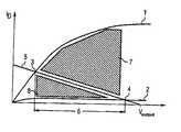
- FIG. 1depicts a current-voltage diagram showing the ON curve 1 and the OFF curve 2 . These characteristic curves correspond to the switched-on and the switched-off states respectively.
- the points of intersection 3 and 4 of the curves with the resistance curve 5correspond to the switching points of the inverter.
- the output voltage swing 6 of the inverteris very large, which means that the inverter can be readily switched on and off.
- the switching currents 7 and 8are different (the shaded areas below the curves correspond to the switching current). This means that the inverter can be quickly switched to “high” but only slowly to “low”.
- FIG. 2again shows the prior art, the second case thereof, in which although the switching currents 9 and 10 are of an equal order of magnitude the voltage level difference 11 is too small. As a result, the corresponding inverter cannot be fully switched off.
- FIG. 3finally shows a current-voltage curve of a logical gate of the invention.
- the current voltage diagram of a logical gate such as is shown in FIG. 3comprises at least one OFET with an extremely thin semi-conducting layer as substitute for a classical resistor.
- OFETs having extremely thin semi-conducting layers of from 5 to 30 nm, preferably from 7 to 25 nm, and more preferably from 10 to 20 nmhave a specific output characteristic field as shown diagrammatically in FIG. 3 .
- the voltage level difference 12is large enough to make it possible to completely switch off the inverter and the switching currents 13 and 14 are identical in size so that the inverter can switch quickly.
- Another advantageis the value of the switching current, which is very high on this type of transistor. Due to the thin semi-conducting layers, the transistors pass from the rising edge 15 very steeply into the saturation region 16 . This behavior of the output characteristic makes it possible to construct logical circuits in conventional p-type MOS technology which show large charging voltages. As a result, the switching speed of the components is high.
- the purpose of the inventionis to utilize this effect for the production of fast logical gates. These gates are fast and can at the same time be easily switch off, despite the use of conventional p-type MOS technology.
- the replacement of the classical resistorcan alternatively be accomplished by special treatment of the semi-conducting layer of an OFET and the use of a special circuit layout for the logic devices.
- Typical OFETshave very low OFF currents when operated without gate potential.
- the basic element of these logic devicesis the connection of at least two OFETs in series of which the flow channels are of different dimensions such that without a gate potential the flow channel of one of the OFETs is distinctly more conductive than that of the other OFET. As a result, the supply voltage applied to the two flow channels only drops in the case of the less conductive flow channel.
- Switchingtakes place by the application of a negative gate potential to the OFET having the less conductive flow channel and the simultaneous application of a positive gate potential to the OFET having the more conductive flow channel.
- FIG. 5shows the current voltage diagram of such a logical gate. Due to the special circuit layout or the special circuit layout in conjunction with a treatment of the semi-conducting layer, both characteristic curves are subjected to a shift, which results in a high voltage level difference and at the same time a high switching current.
- An invertercomprises two of these basic elements, ie it has at least four transistors. The switching operation of the inverter is achieved by switching on two of the transistors and at the same time switching off the other two.
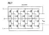
- FIG. 6shows the circuit of an inverter and FIG. 7 the circuit of a ring oscillator.
- two pairs of transistorsare required, since a positive voltage is required to switch off one transistor and at the same time a negative voltage to switch on the other.
- two of the aforementioned basic elementsare interconnected such that one will provide a positive voltage at its output and the other a negative voltage.
- An inverter based on this novel circuit technologythus has two inputs and two outputs, the potential at the outputs of each will be zero (0 V) or a positive or negative voltage (+/ ⁇ V).
- FIG. 6shows the inverter embodiment, in which the circuitry is an important factor.
- the supply voltageis available at point 1 , which in this case is +/ ⁇ V.
- Point 4is the ground connection.
- the points denoted by 3symbolize the inputs and those denoted by 2 symbolize the outputs of the inverter.
- Logical “low”is achieved when no potential is available at the outputs 2 .
- Logical “high”means that +/ ⁇ V are available at the output 2 of the inverter. That is to say, the data line comprises two lines, on which different potentials are available.
- C-type MOSsuse an input which is split, but the potential is the same after splitting.
- a conventional c-type MOS inverterfor example, consists of two transistors.
- transistor 1When there is OV at the input, transistor 1 is conductive and the other, 2 , is non-conductive (the supply voltage thus drops at 2 ).
- the supply voltageWhen there is a negative potential, 1 will be non-conductive and 2 will be conductive (the supply voltage is thus available at 1 )
- FIG. 7shows a ring oscillator.
- an uneven number of invertersare interconnected by connecting the output of one to the input of the next inverter.
- the last inverteris then connected in like fashion to the first inverter so as to form a ring.
- the purpose of a ring oscillatoris to allow the signal to pass continuously through the ring by constant switching of the succeeding inverter.
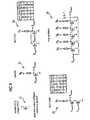
- FIG. 4shows some embodiments of the logic components comprising OFETs having ex-tremely thin semi-conducting layers:
- Inverter 22Inverter 22 , NOT-OR 23 , NOT-AND 24 , ring oscillator 25 .
- the graphical symbol 21symbolizes a p-type OFET.
- An inverter 22can be a transistor connected to a resistor.
- a signal (“high” or “low”) applied to the inputis reversed (inverted) and then made available at the output (as “low” or “high”).
- a NOT-ANDcan be realized in analogous manner by connecting the transistors in series.
- Another embodimentis a logical gate, eg, a flip-flop, which could be formed from these OFETs.
- the logical gatesare produced by (spray) coating, knife coating, printing or some other manufacturing process, which may be carried out as a continuous process.
- the inventionmakes it possible, for the first time, to produce, despite conventional p-type MOS technology, fast logical gates built up of organic field effect transistors. This is primarily due to the early saturation effect of OFETs having very thin semi-conducting layers, and, furthermore, to the use of OFETs having specific properties as the organic logic components and to a novel layout of the circuit containing these logic components.
Landscapes
- Logic Circuits (AREA)
- Metal-Oxide And Bipolar Metal-Oxide Semiconductor Integrated Circuits (AREA)
Abstract
Description
- The invention relates to logic components comprising organic field effect transistors, the switching speed of which is increased by replacing the resistors.
- Logical gates such as NAND, NOR, or inverters are the elementary components of an integrated digital electronic circuit. The switching speed of the integrated circuit depends on the speed of the logical gates and not on the speed of the individual transistors. In conventional silicon semiconductor technology these gates are made using both n-type and p-type transistors and are thus very quick-acting. In the case of organic circuits this cannot be achieved because there are no adequately stable n-type semiconductors. This means that organic circuits have to include a conventional resistor instead of the n-type transistor.
- A disadvantage of these logical gates made up of organic field effect transistors is that either they switch slowly (when the switching current, ie the integrals below the current voltage characteristic, differ considerably) or they cannot be switched off (when the voltage level difference in the current-voltage diagram is too small.
- It is thus an object of the present invention to provide a logical gate made up of organic field effect transistors, in which the missing “classical” n-type transistors are replaced by components other than classical resistors.
- The present invention relates to a logical gate comprising at least one first and one second organic field effect transistor (OFET), in which the first OFET is a p-type OFET and the second OFET can serve in the logical gate as a resistor.
- According to one embodiment, the first OFET has an extremely thin semi-conducting layer or a negative threshold voltage.
- According to another embodiment the logical gate comprises first and second OFETs each having an extremely thin semi-conducting layer or a negative threshold voltage.
- According to a further embodiment, the second OFET without gate potential in the logical gate has OFF currents that are only approximately one order of magnitude lower than the ON currents so that the second OFET can be switched off by applying a positive gate potential.
- According to one embodiment, the logical gate comprises at least four OFETs (cf
FIG. 6 ). - According to another embodiment, the
logical gate 2 has data lines (input and output), which have different potentials. By an “OFET that can serve in the gate as a resistor” is meant in this case either an OFET which has an extremely thin organic semi-conducting layer (ca from 5 to 30 nm) or an OFET in which the conductivity of the organic semi-conducting layer is reduced by special treatment (for example hydrazine treatment and/or special oxidation) such that the OFF currents are lower than the ON currents by only approximately one order of magnitude. - The “OFF current” is the current which flows when there is no potential between the gate electrode and the source electrode and the “ON current” (for p-type OFETs) is the current which flows when there is a negative potential difference between the gate electrode and the source electrode.
- By a “classical resistor” we mean here a component having a linear current-voltage curve.
- The invention is explained in greater detail below with reference to the drawings.
- When a classical resistor is used (cf
FIGS. 1 and 2 , prior art) the logical gates switch either too slowly (FIG. 1 ) or cannot be switched off(FIG. 2 ). FIG. 1 depicts a current-voltage diagram showing theON curve 1 and theOFF curve 2. These characteristic curves correspond to the switched-on and the switched-off states respectively. The points ofintersection resistance curve 5 correspond to the switching points of the inverter. Theoutput voltage swing 6 of the inverter is very large, which means that the inverter can be readily switched on and off. However, theswitching currents 7 and8 are different (the shaded areas below the curves correspond to the switching current). This means that the inverter can be quickly switched to “high” but only slowly to “low”.FIG. 2 again shows the prior art, the second case thereof, in which although theswitching currents 9 and10 are of an equal order of magnitude thevoltage level difference 11 is too small. As a result, the corresponding inverter cannot be fully switched off.FIG. 3 finally shows a current-voltage curve of a logical gate of the invention.- The current voltage diagram of a logical gate such as is shown in
FIG. 3 comprises at least one OFET with an extremely thin semi-conducting layer as substitute for a classical resistor. - Due to an observed but not fully explained effect (very early saturation by reason of a very thin semiconductor layer or a negative threshold voltage), OFETs having extremely thin semi-conducting layers of from 5 to 30 nm, preferably from 7 to 25 nm, and more preferably from 10 to 20 nm have a specific output characteristic field as shown diagrammatically in
FIG. 3 . - The
voltage level difference 12 is large enough to make it possible to completely switch off the inverter and theswitching currents edge 15 very steeply into thesaturation region 16. This behavior of the output characteristic makes it possible to construct logical circuits in conventional p-type MOS technology which show large charging voltages. As a result, the switching speed of the components is high. The purpose of the invention is to utilize this effect for the production of fast logical gates. These gates are fast and can at the same time be easily switch off, despite the use of conventional p-type MOS technology. - The replacement of the classical resistor can alternatively be accomplished by special treatment of the semi-conducting layer of an OFET and the use of a special circuit layout for the logic devices.
- Typical OFETs have very low OFF currents when operated without gate potential.
- Special treatment of the organic semi-conductor can cause the OFF currents to be only approximately one order of magnitude lower than the ON currents (for example by hydrazine treatment or by special oxidation). These particular OFETs can then still be switched off by the application of a positive gate potential. This provides an OFET that can be switched on by a negative gate potential and switched off by a positive gate potential (like an n-type transistor). This effect is utilized by the invention (in addition to the aforementioned effect arising from extremely thin semi-conducting layers), in order to produce fast logic devices. The basic element of these logic devices is the connection of at least two OFETs in series of which the flow channels are of different dimensions such that without a gate potential the flow channel of one of the OFETs is distinctly more conductive than that of the other OFET. As a result, the supply voltage applied to the two flow channels only drops in the case of the less conductive flow channel.
- Switching takes place by the application of a negative gate potential to the OFET having the less conductive flow channel and the simultaneous application of a positive gate potential to the OFET having the more conductive flow channel.
FIG. 5 shows the current voltage diagram of such a logical gate. Due to the special circuit layout or the special circuit layout in conjunction with a treatment of the semi-conducting layer, both characteristic curves are subjected to a shift, which results in a high voltage level difference and at the same time a high switching current. An inverter comprises two of these basic elements, ie it has at least four transistors. The switching operation of the inverter is achieved by switching on two of the transistors and at the same time switching off the other two.- The invention is explained below with reference to a number of embodiments:
- First of all we will deal with two embodiments relating to the current voltage diagram shown in
FIG. 5 : FIG. 6 shows the circuit of an inverter andFIG. 7 the circuit of a ring oscillator. In order to obtain logically functional components, two pairs of transistors are required, since a positive voltage is required to switch off one transistor and at the same time a negative voltage to switch on the other. In order to obtain these different voltages, two of the aforementioned basic elements are interconnected such that one will provide a positive voltage at its output and the other a negative voltage. An inverter based on this novel circuit technology thus has two inputs and two outputs, the potential at the outputs of each will be zero (0 V) or a positive or negative voltage (+/−V).FIG. 6 shows the inverter embodiment, in which the circuitry is an important factor. The supply voltage is available atpoint 1, which in this case is +/−V. Point 4 is the ground connection. The points denoted by 3 symbolize the inputs and those denoted by 2 symbolize the outputs of the inverter. Logical “low” is achieved when no potential is available at theoutputs 2. Logical “high” means that +/−V are available at theoutput 2 of the inverter. That is to say, the data line comprises two lines, on which different potentials are available.- C-type MOSs use an input which is split, but the potential is the same after splitting.
- Unlike the aforementioned inverter, which has at least four OFETs, a conventional c-type MOS inverter, for example, consists of two transistors. When there is OV at the input,
transistor 1 is conductive and the other,2, is non-conductive (the supply voltage thus drops at2). When there is a negative potential,1 will be non-conductive and2 will be conductive (the supply voltage is thus available at1) FIG. 7 shows a ring oscillator. For this circuit an uneven number of inverters are interconnected by connecting the output of one to the input of the next inverter. The last inverter is then connected in like fashion to the first inverter so as to form a ring. The purpose of a ring oscillator is to allow the signal to pass continuously through the ring by constant switching of the succeeding inverter.FIG. 4 shows some embodiments of the logic components comprising OFETs having ex-tremely thin semi-conducting layers:Inverter 22, NOT-OR23, NOT-AND24,ring oscillator 25. Thegraphical symbol 21 symbolizes a p-type OFET.- An
inverter 22 can be a transistor connected to a resistor. A signal (“high” or “low”) applied to the input is reversed (inverted) and then made available at the output (as “low” or “high”). In order to obtain a logical NOT-OR, two transistors can be connected in parallel. The states are passed on to the output by the application of an input voltage according to the table “low ”=“0 “; “high ”=“1 ”). A NOT-AND can be realized in analogous manner by connecting the transistors in series. - Another embodiment (not shown) is a logical gate, eg, a flip-flop, which could be formed from these OFETs.
- Advantageously, the logical gates are produced by (spray) coating, knife coating, printing or some other manufacturing process, which may be carried out as a continuous process.
- The invention makes it possible, for the first time, to produce, despite conventional p-type MOS technology, fast logical gates built up of organic field effect transistors. This is primarily due to the early saturation effect of OFETs having very thin semi-conducting layers, and, furthermore, to the use of OFETs having specific properties as the organic logic components and to a novel layout of the circuit containing these logic components.
Claims (11)
Applications Claiming Priority (4)
| Application Number | Priority Date | Filing Date | Title |
|---|---|---|---|
| DE10212640ADE10212640B4 (en) | 2002-03-21 | 2002-03-21 | Logical components made of organic field effect transistors |
| DE10212640.2 | 2002-03-21 | ||
| DE10212640 | 2002-03-21 | ||
| PCT/DE2003/000843WO2003081671A2 (en) | 2002-03-21 | 2003-03-14 | Logic components from organic field effect transistors |
Publications (2)
| Publication Number | Publication Date |
|---|---|
| US20050277240A1true US20050277240A1 (en) | 2005-12-15 |
| US7223995B2 US7223995B2 (en) | 2007-05-29 |
Family
ID=28050743
Family Applications (1)
| Application Number | Title | Priority Date | Filing Date |
|---|---|---|---|
| US10/508,640Expired - Fee RelatedUS7223995B2 (en) | 2002-03-21 | 2003-03-14 | Logic components comprising organic field effect transistors |
Country Status (6)
| Country | Link |
|---|---|
| US (1) | US7223995B2 (en) |
| EP (1) | EP1502301A2 (en) |
| JP (1) | JP4171703B2 (en) |
| CN (1) | CN100361389C (en) |
| DE (1) | DE10212640B4 (en) |
| WO (1) | WO2003081671A2 (en) |
Cited By (2)
| Publication number | Priority date | Publication date | Assignee | Title |
|---|---|---|---|---|
| US20030183817A1 (en)* | 2000-09-01 | 2003-10-02 | Adolf Bernds | Organic field effect transistor, method for structuring an ofet and integrated circuit |
| US20070290759A1 (en)* | 2006-05-30 | 2007-12-20 | Stmicroelectronics S.R.L. | Analog transconductance amplifier |
Families Citing this family (26)
| Publication number | Priority date | Publication date | Assignee | Title |
|---|---|---|---|---|
| DE10061299A1 (en) | 2000-12-08 | 2002-06-27 | Siemens Ag | Device for determining and / or forwarding at least one environmental influence, production method and use thereof |
| DE10061297C2 (en) | 2000-12-08 | 2003-05-28 | Siemens Ag | Procedure for structuring an OFET |
| DE10105914C1 (en) | 2001-02-09 | 2002-10-10 | Siemens Ag | Organic field effect transistor with photo-structured gate dielectric and a method for its production |
| DE10151036A1 (en) | 2001-10-16 | 2003-05-08 | Siemens Ag | Isolator for an organic electronic component |
| DE10151440C1 (en) | 2001-10-18 | 2003-02-06 | Siemens Ag | Organic electronic component for implementing an encapsulated partially organic electronic component has components like a flexible foil as an antenna, a diode or capacitor and an organic transistor. |
| DE10160732A1 (en) | 2001-12-11 | 2003-06-26 | Siemens Ag | OFET used e.g. in RFID tag, comprises an intermediate layer on an active semiconductor layer |
| DE10212640B4 (en) | 2002-03-21 | 2004-02-05 | Siemens Ag | Logical components made of organic field effect transistors |
| DE10253154A1 (en) | 2002-11-14 | 2004-05-27 | Siemens Ag | Biosensor, used to identify analyte in liquid sample, has test field with detector, where detector registers field changes as electrical signals for evaluation |
| EP1563553B1 (en) | 2002-11-19 | 2007-02-14 | PolyIC GmbH & Co. KG | Organic electronic circuitcomprising a structured, semi-conductive functional layer and a method for producing said component |
| DE10302149A1 (en) | 2003-01-21 | 2005-08-25 | Siemens Ag | Use of conductive carbon black / graphite blends for the production of low-cost electronics |
| DE10330064B3 (en)* | 2003-07-03 | 2004-12-09 | Siemens Ag | Organic logic gate has load field effect transistor with potential-free gate electrode in series with switching field effect transistor |
| DE10339036A1 (en) | 2003-08-25 | 2005-03-31 | Siemens Ag | Organic electronic component with high-resolution structuring and manufacturing method |
| DE10340644B4 (en) | 2003-09-03 | 2010-10-07 | Polyic Gmbh & Co. Kg | Mechanical controls for organic polymer electronics |
| US20050156656A1 (en)* | 2004-01-15 | 2005-07-21 | Rotzoll Robert R. | Non-quasistatic rectifier circuit |
| DE102004059467A1 (en)* | 2004-12-10 | 2006-07-20 | Polyic Gmbh & Co. Kg | Gate made of organic field effect transistors |
| DE102005009819A1 (en)* | 2005-03-01 | 2006-09-07 | Polyic Gmbh & Co. Kg | electronics assembly |
| DE102005009820A1 (en)* | 2005-03-01 | 2006-09-07 | Polyic Gmbh & Co. Kg | Electronic assembly with organic logic switching elements |
| DE102005017655B4 (en) | 2005-04-15 | 2008-12-11 | Polyic Gmbh & Co. Kg | Multilayer composite body with electronic function |
| DE102005031448A1 (en) | 2005-07-04 | 2007-01-11 | Polyic Gmbh & Co. Kg | Activatable optical layer |
| DE102005035590A1 (en)* | 2005-07-29 | 2007-02-01 | Polyic Gmbh & Co. Kg | Electronic component has flexible substrate and stack of layers including function layer on substratesurface |
| DE102005035589A1 (en) | 2005-07-29 | 2007-02-01 | Polyic Gmbh & Co. Kg | Manufacturing electronic component on surface of substrate where component has two overlapping function layers |
| DE102005042166A1 (en)* | 2005-09-06 | 2007-03-15 | Polyic Gmbh & Co.Kg | Organic device and such a comprehensive electrical circuit |
| DE102005044306A1 (en)* | 2005-09-16 | 2007-03-22 | Polyic Gmbh & Co. Kg | Electronic circuit and method for producing such |
| US20090004368A1 (en)* | 2007-06-29 | 2009-01-01 | Weyerhaeuser Co. | Systems and methods for curing a deposited layer on a substrate |
| DE102007059231A1 (en)* | 2007-12-07 | 2009-06-10 | Polyic Gmbh & Co. Kg | Electronic assembly with organic switching elements |
| US8463116B2 (en)* | 2008-07-01 | 2013-06-11 | Tap Development Limited Liability Company | Systems for curing deposited material using feedback control |
Citations (90)
| Publication number | Priority date | Publication date | Assignee | Title |
|---|---|---|---|---|
| US18911A (en)* | 1857-12-22 | Glass knob for doors | ||
| US3512052A (en)* | 1968-01-11 | 1970-05-12 | Gen Motors Corp | Metal-insulator-semiconductor voltage variable capacitor with controlled resistivity dielectric |
| US3769096A (en)* | 1971-03-12 | 1973-10-30 | Bell Telephone Labor Inc | Pyroelectric devices |
| US3955098A (en)* | 1973-10-12 | 1976-05-04 | Hitachi, Ltd. | Switching circuit having floating gate mis load transistors |
| US4302648A (en)* | 1978-01-26 | 1981-11-24 | Shin-Etsu Polymer Co., Ltd. | Key-board switch unit |
| US4340657A (en)* | 1980-02-19 | 1982-07-20 | Polychrome Corporation | Novel radiation-sensitive articles |
| US4442019A (en)* | 1978-05-26 | 1984-04-10 | Marks Alvin M | Electroordered dipole suspension |
| US4865197A (en)* | 1988-03-04 | 1989-09-12 | Unisys Corporation | Electronic component transportation container |
| US4926052A (en)* | 1986-03-03 | 1990-05-15 | Kabushiki Kaisha Toshiba | Radiation detecting device |
| US4937119A (en)* | 1988-12-15 | 1990-06-26 | Hoechst Celanese Corp. | Textured organic optical data storage media and methods of preparation |
| US5173835A (en)* | 1991-10-15 | 1992-12-22 | Motorola, Inc. | Voltage variable capacitor |
| US5206525A (en)* | 1989-12-27 | 1993-04-27 | Nippon Petrochemicals Co., Ltd. | Electric element capable of controlling the electric conductivity of π-conjugated macromolecular materials |
| US5259926A (en)* | 1991-09-24 | 1993-11-09 | Hitachi, Ltd. | Method of manufacturing a thin-film pattern on a substrate |
| US5321240A (en)* | 1992-01-30 | 1994-06-14 | Mitsubishi Denki Kabushiki Kaisha | Non-contact IC card |
| US5347144A (en)* | 1990-07-04 | 1994-09-13 | Centre National De La Recherche Scientifique (Cnrs) | Thin-layer field-effect transistors with MIS structure whose insulator and semiconductor are made of organic materials |
| US5364735A (en)* | 1988-07-01 | 1994-11-15 | Sony Corporation | Multiple layer optical record medium with protective layers and method for producing same |
| US5395504A (en)* | 1993-02-04 | 1995-03-07 | Asulab S.A. | Electrochemical measuring system with multizone sensors |
| US5480839A (en)* | 1993-01-15 | 1996-01-02 | Kabushiki Kaisha Toshiba | Semiconductor device manufacturing method |
| US5486851A (en)* | 1991-10-30 | 1996-01-23 | Fraunhofer-Gesellschaft Zur Forderung Der Angewandten Forschung E.V. | Illumination device using a pulsed laser source a Schlieren optical system and a matrix addressable surface light modulator for producing images with undifracted light |
| US5502396A (en)* | 1993-09-21 | 1996-03-26 | Asulab S.A. | Measuring device with connection for a removable sensor |
| US5546889A (en)* | 1993-10-06 | 1996-08-20 | Matsushita Electric Industrial Co., Ltd. | Method of manufacturing organic oriented film and method of manufacturing electronic device |
| US5569879A (en)* | 1991-02-19 | 1996-10-29 | Gemplus Card International | Integrated circuit micromodule obtained by the continuous assembly of patterned strips |
| US5574291A (en)* | 1994-12-09 | 1996-11-12 | Lucent Technologies Inc. | Article comprising a thin film transistor with low conductivity organic layer |
| US5578513A (en)* | 1993-09-17 | 1996-11-26 | Mitsubishi Denki Kabushiki Kaisha | Method of making a semiconductor device having a gate all around type of thin film transistor |
| US5580794A (en)* | 1993-08-24 | 1996-12-03 | Metrika Laboratories, Inc. | Disposable electronic assay device |
| US5625199A (en)* | 1996-01-16 | 1997-04-29 | Lucent Technologies Inc. | Article comprising complementary circuit with inorganic n-channel and organic p-channel thin film transistors |
| US5629530A (en)* | 1994-05-16 | 1997-05-13 | U.S. Phillips Corporation | Semiconductor device having an organic semiconductor material |
| US5630986A (en)* | 1995-01-13 | 1997-05-20 | Bayer Corporation | Dispensing instrument for fluid monitoring sensors |
| US5652645A (en)* | 1995-07-24 | 1997-07-29 | Anvik Corporation | High-throughput, high-resolution, projection patterning system for large, flexible, roll-fed, electronic-module substrates |
| US5691089A (en)* | 1993-03-25 | 1997-11-25 | Texas Instruments Incorporated | Integrated circuits formed in radiation sensitive material and method of forming same |
| US5705826A (en)* | 1994-06-28 | 1998-01-06 | Hitachi, Ltd. | Field-effect transistor having a semiconductor layer made of an organic compound |
| US5729428A (en)* | 1995-04-25 | 1998-03-17 | Nec Corporation | Solid electrolytic capacitor with conductive polymer as solid electrolyte and method for fabricating the same |
| US5869972A (en)* | 1996-02-26 | 1999-02-09 | Birch; Brian Jeffrey | Testing device using a thermochromic display and method of using same |
| US5883397A (en)* | 1993-07-01 | 1999-03-16 | Mitsubishi Denki Kabushiki Kaisha | Plastic functional element |
| US5892244A (en)* | 1989-01-10 | 1999-04-06 | Mitsubishi Denki Kabushiki Kaisha | Field effect transistor including πconjugate polymer and liquid crystal display including the field effect transistor |
| US5946551A (en)* | 1997-03-25 | 1999-08-31 | Dimitrakopoulos; Christos Dimitrios | Fabrication of thin film effect transistor comprising an organic semiconductor and chemical solution deposited metal oxide gate dielectric |
| US5970318A (en)* | 1997-05-15 | 1999-10-19 | Electronics And Telecommunications Research Institute | Fabrication method of an organic electroluminescent devices |
| US5967048A (en)* | 1998-06-12 | 1999-10-19 | Howard A. Fromson | Method and apparatus for the multiple imaging of a continuous web |
| US5973598A (en)* | 1997-09-11 | 1999-10-26 | Precision Dynamics Corporation | Radio frequency identification tag on flexible substrate |
| US5997817A (en)* | 1997-12-05 | 1999-12-07 | Roche Diagnostics Corporation | Electrochemical biosensor test strip |
| US5998805A (en)* | 1997-12-11 | 1999-12-07 | Motorola, Inc. | Active matrix OED array with improved OED cathode |
| US6036919A (en)* | 1996-07-23 | 2000-03-14 | Roche Diagnostic Gmbh | Diagnostic test carrier with multilayer field |
| US6045977A (en)* | 1998-02-19 | 2000-04-04 | Lucent Technologies Inc. | Process for patterning conductive polyaniline films |
| US6072716A (en)* | 1999-04-14 | 2000-06-06 | Massachusetts Institute Of Technology | Memory structures and methods of making same |
| US6083104A (en)* | 1998-01-16 | 2000-07-04 | Silverlit Toys (U.S.A.), Inc. | Programmable toy with an independent game cartridge |
| US6087196A (en)* | 1998-01-30 | 2000-07-11 | The Trustees Of Princeton University | Fabrication of organic semiconductor devices using ink jet printing |
| US6133835A (en)* | 1997-12-05 | 2000-10-17 | U.S. Philips Corporation | Identification transponder |
| US6150668A (en)* | 1998-05-29 | 2000-11-21 | Lucent Technologies Inc. | Thin-film transistor monolithically integrated with an organic light-emitting diode |
| US6197663B1 (en)* | 1999-12-07 | 2001-03-06 | Lucent Technologies Inc. | Process for fabricating integrated circuit devices having thin film transistors |
| US6207472B1 (en)* | 1999-03-09 | 2001-03-27 | International Business Machines Corporation | Low temperature thin film transistor fabrication |
| US6215130B1 (en)* | 1998-08-20 | 2001-04-10 | Lucent Technologies Inc. | Thin film transistors |
| US6221553B1 (en)* | 1999-01-15 | 2001-04-24 | 3M Innovative Properties Company | Thermal transfer element for forming multilayer devices |
| US6251513B1 (en)* | 1997-11-08 | 2001-06-26 | Littlefuse, Inc. | Polymer composites for overvoltage protection |
| US6284562B1 (en)* | 1999-11-17 | 2001-09-04 | Agere Systems Guardian Corp. | Thin film transistors |
| US6300141B1 (en)* | 1999-03-02 | 2001-10-09 | Helix Biopharma Corporation | Card-based biosensor device |
| US6321571B1 (en)* | 1998-12-21 | 2001-11-27 | Corning Incorporated | Method of making glass structures for flat panel displays |
| US6322736B1 (en)* | 1998-03-27 | 2001-11-27 | Agere Systems Inc. | Method for fabricating molded microstructures on substrates |
| US6329226B1 (en)* | 2000-06-01 | 2001-12-11 | Agere Systems Guardian Corp. | Method for fabricating a thin-film transistor |
| US6330464B1 (en)* | 1998-08-26 | 2001-12-11 | Sensors For Medicine & Science | Optical-based sensing devices |
| US6335539B1 (en)* | 1999-11-05 | 2002-01-01 | International Business Machines Corporation | Method for improving performance of organic semiconductors in bottom electrode structure |
| US6340822B1 (en)* | 1999-10-05 | 2002-01-22 | Agere Systems Guardian Corp. | Article comprising vertically nano-interconnected circuit devices and method for making the same |
| US6344662B1 (en)* | 1997-03-25 | 2002-02-05 | International Business Machines Corporation | Thin-film field-effect transistor with organic-inorganic hybrid semiconductor requiring low operating voltages |
| US20020022284A1 (en)* | 1991-02-27 | 2002-02-21 | Alan J. Heeger | Visible light emitting diodes fabricated from soluble semiconducting polymers |
| US20020025391A1 (en)* | 1989-05-26 | 2002-02-28 | Marie Angelopoulos | Patterns of electrically conducting polymers and their application as electrodes or electrical contacts |
| US6362509B1 (en)* | 1999-10-11 | 2002-03-26 | U.S. Philips Electronics | Field effect transistor with organic semiconductor layer |
| US6384804B1 (en)* | 1998-11-25 | 2002-05-07 | Lucent Techonologies Inc. | Display comprising organic smart pixels |
| US20020053320A1 (en)* | 1998-12-15 | 2002-05-09 | Gregg M. Duthaler | Method for printing of transistor arrays on plastic substrates |
| US20020056839A1 (en)* | 2000-11-11 | 2002-05-16 | Pt Plus Co. Ltd. | Method of crystallizing a silicon thin film and semiconductor device fabricated thereby |
| US20020068392A1 (en)* | 2000-12-01 | 2002-06-06 | Pt Plus Co. Ltd. | Method for fabricating thin film transistor including crystalline silicon active layer |
| US6403396B1 (en)* | 1998-01-28 | 2002-06-11 | Thin Film Electronics Asa | Method for generation of electrically conducting or semiconducting structures in three dimensions and methods for erasure of the same structures |
| US6429450B1 (en)* | 1997-08-22 | 2002-08-06 | Koninklijke Philips Electronics N.V. | Method of manufacturing a field-effect transistor substantially consisting of organic materials |
| US20020130042A1 (en)* | 2000-03-02 | 2002-09-19 | Moerman Piet H.C. | Combined lancet and electrochemical analyte-testing apparatus |
| US20020170897A1 (en)* | 2001-05-21 | 2002-11-21 | Hall Frank L. | Methods for preparing ball grid array substrates via use of a laser |
| US6498114B1 (en)* | 1999-04-09 | 2002-12-24 | E Ink Corporation | Method for forming a patterned semiconductor film |
| US20020195644A1 (en)* | 2001-06-08 | 2002-12-26 | Ananth Dodabalapur | Organic polarizable gate transistor apparatus and method |
| US6517955B1 (en)* | 1999-02-22 | 2003-02-11 | Nippon Steel Corporation | High strength galvanized steel plate excellent in adhesion of plated metal and formability in press working and high strength alloy galvanized steel plate and method for production thereof |
| US20030059987A1 (en)* | 1999-12-21 | 2003-03-27 | Plastic Logic Limited | Inkjet-fabricated integrated circuits |
| US6555840B1 (en)* | 1999-02-16 | 2003-04-29 | Sharp Kabushiki Kaisha | Charge-transport structures |
| US20030112576A1 (en)* | 2001-09-28 | 2003-06-19 | Brewer Peter D. | Process for producing high performance interconnects |
| US6593690B1 (en)* | 1999-09-03 | 2003-07-15 | 3M Innovative Properties Company | Large area organic electronic devices having conducting polymer buffer layers and methods of making same |
| US6603139B1 (en)* | 1998-04-16 | 2003-08-05 | Cambridge Display Technology Limited | Polymer devices |
| US6621098B1 (en)* | 1999-11-29 | 2003-09-16 | The Penn State Research Foundation | Thin-film transistor and methods of manufacturing and incorporating a semiconducting organic material |
| US20040002176A1 (en)* | 2002-06-28 | 2004-01-01 | Xerox Corporation | Organic ferroelectric memory cells |
| US20040013982A1 (en)* | 1999-09-14 | 2004-01-22 | Massachusetts Institute Of Technology | Fabrication of finely featured devices by liquid embossing |
| US20040026689A1 (en)* | 2000-08-18 | 2004-02-12 | Adolf Bernds | Encapsulated organic-electronic component, method for producing the same and use thereof |
| US20040084670A1 (en)* | 2002-11-04 | 2004-05-06 | Tripsas Nicholas H. | Stacked organic memory devices and methods of operating and fabricating |
| US20040211329A1 (en)* | 2001-09-18 | 2004-10-28 | Katsuyuki Funahata | Pattern forming method and pattern forming device |
| US6852583B2 (en)* | 2000-07-07 | 2005-02-08 | Siemens Aktiengesellschaft | Method for the production and configuration of organic field-effect transistors (OFET) |
| US6854139B2 (en)* | 2002-07-26 | 2005-02-15 | Sheila Lamy | Bed covering fastening system |
| US6903958B2 (en)* | 2000-09-13 | 2005-06-07 | Siemens Aktiengesellschaft | Method of writing to an organic memory |
Family Cites Families (108)
| Publication number | Priority date | Publication date | Assignee | Title |
|---|---|---|---|---|
| GB723598A (en) | 1951-09-07 | 1955-02-09 | Philips Nv | Improvements in or relating to methods of producing electrically conductive mouldings from plastics |
| JPS5638918Y2 (en) | 1977-10-25 | 1981-09-10 | ||
| JPS5641938U (en) | 1979-09-10 | 1981-04-17 | ||
| CA1169639A (en) | 1981-06-16 | 1984-06-26 | Tomasz S. Hope | Laying of optical waveguides onto a support filament |
| JPS5846719U (en) | 1981-09-25 | 1983-03-29 | 本州ダンボ−ル工業株式会社 | tray |
| DE3321071A1 (en) | 1983-06-10 | 1984-12-13 | Basf Ag | PRESSURE SWITCH |
| DE3338597A1 (en) | 1983-10-24 | 1985-05-02 | GAO Gesellschaft für Automation und Organisation mbH, 8000 München | DATA CARRIER WITH INTEGRATED CIRCUIT AND METHOD FOR PRODUCING THE SAME |
| JPS60117769A (en) | 1983-11-30 | 1985-06-25 | Fujitsu Ltd | semiconductor memory device |
| JPS61167854U (en) | 1985-04-10 | 1986-10-17 | ||
| DE3751376T2 (en) | 1986-10-13 | 1995-11-16 | Canon Kk | Circuit element. |
| JP2728412B2 (en) | 1987-12-25 | 1998-03-18 | 株式会社日立製作所 | Semiconductor device |
| DE68912426T2 (en) | 1988-06-21 | 1994-05-11 | Gec Avery Ltd | Manufacture of portable electronic cards. |
| EP0418504B1 (en) | 1989-07-25 | 1995-04-05 | Matsushita Electric Industrial Co., Ltd. | Organic semiconductor memory device having a MISFET structure and its control method |
| FI91573C (en) | 1990-01-04 | 1994-07-11 | Neste Oy | Ways of producing electronic and electro-optical components and circuits |
| US5376561A (en) | 1990-12-31 | 1994-12-27 | Kopin Corporation | High density electronic circuit modules |
| EP0501456A3 (en) | 1991-02-26 | 1992-09-09 | Sony Corporation | Video game computer provided with an optical disc drive |
| JP3522771B2 (en)* | 1991-03-22 | 2004-04-26 | 三菱電機株式会社 | Inverter |
| US5332315A (en) | 1991-04-27 | 1994-07-26 | Gec Avery Limited | Apparatus and sensor unit for monitoring changes in a physical quantity with time |
| JP2714278B2 (en) | 1991-08-20 | 1998-02-16 | 三井化学株式会社 | Filter and its manufacturing device |
| JP3150750B2 (en) | 1992-03-13 | 2001-03-26 | 日本写真印刷株式会社 | Organic rectifier |
| JPH05347422A (en) | 1992-06-16 | 1993-12-27 | Fujitsu Ltd | Bistable diode |
| JP2685652B2 (en) | 1992-09-25 | 1997-12-03 | 日本碍子株式会社 | Solid insulator and method for manufacturing the same |
| DE4243832A1 (en) | 1992-12-23 | 1994-06-30 | Daimler Benz Ag | Push button arrangement |
| WO1994017556A1 (en) | 1993-01-26 | 1994-08-04 | Fci-Fiberchem, Inc. | Optical sensor with electroluminescent light source and polymer light detector |
| IL111151A (en) | 1994-10-03 | 1998-09-24 | News Datacom Ltd | Secure access systems |
| DE69506215T2 (en) | 1994-05-18 | 1999-06-10 | Koninklijke Philips Electronics N.V., Eindhoven | METHOD FOR PRODUCING A THIN LAYER FROM CONJUGED, SUBSTITUTED OR NON-SUBSTITUTED POLY (P-PHENYLENE VINYLENE) BY GAS PHASE DEPOSITION, AND PRODUCTION METHOD OF AN ELECTROLUMINESCENTING DEVICE |
| US5684884A (en) | 1994-05-31 | 1997-11-04 | Hitachi Metals, Ltd. | Piezoelectric loudspeaker and a method for manufacturing the same |
| WO1996002924A1 (en) | 1994-07-14 | 1996-02-01 | Surgx Corporation | Single and multi-layer variable voltage protection devices and methods of making same |
| US5707745A (en) | 1994-12-13 | 1998-01-13 | The Trustees Of Princeton University | Multicolor organic light emitting devices |
| JPH08197788A (en) | 1995-01-27 | 1996-08-06 | Hitachi Koki Co Ltd | Image data read circuit of printer controller |
| JPH0983040A (en) | 1995-09-12 | 1997-03-28 | Sharp Corp | Thin film transistor and manufacturing method thereof |
| GB9519698D0 (en) | 1995-09-27 | 1995-11-29 | Rivaz Antony C De | Educational toys and games |
| WO1997018944A1 (en) | 1995-11-22 | 1997-05-29 | The Government Of The United States Of America, Represented By The Secretary Of The Navy | Patterned conducting polymer surfaces and process for preparing the same and devices containing the same |
| US6326640B1 (en) | 1996-01-29 | 2001-12-04 | Motorola, Inc. | Organic thin film transistor with enhanced carrier mobility |
| JPH09320760A (en) | 1996-05-24 | 1997-12-12 | Matsushita Electric Ind Co Ltd | Patterning method for organic thin film electroluminescent device |
| JPH1026934A (en) | 1996-07-12 | 1998-01-27 | Toshiba Chem Corp | Electronic tag and its manufacturing method |
| DE19644254A1 (en) | 1996-10-24 | 1998-05-07 | Steag Micro Tech Gmbh | Device for treating substrates |
| US6181287B1 (en) | 1997-03-10 | 2001-01-30 | Precision Dynamics Corporation | Reactively coupled elements in circuits on flexible substrates |
| GB9715907D0 (en) | 1997-07-29 | 1997-10-01 | Cambridge Consultants | Electroluminescent device production process |
| WO1999010929A2 (en)* | 1997-08-22 | 1999-03-04 | Koninklijke Philips Electronics N.V. | A method of providing a vertical interconnect between thin film microelectronic devices |
| EP1029369A4 (en) | 1997-10-17 | 2002-04-03 | Univ California | INK-JET PRINTING METHOD FOR THE PRODUCTION OF ORGANIC SEMICONDUCTOR ARRANGEMENTS |
| JPH11142810A (en) | 1997-11-12 | 1999-05-28 | Nintendo Co Ltd | Portable information processor |
| NO306529B1 (en) | 1998-01-16 | 1999-11-15 | Opticom As | Transistor |
| DE19816860A1 (en) | 1998-03-06 | 1999-11-18 | Deutsche Telekom Ag | Chip card, especially credit card |
| US6518949B2 (en) | 1998-04-10 | 2003-02-11 | E Ink Corporation | Electronic displays using organic-based field effect transistors |
| GB9808806D0 (en) | 1998-04-24 | 1998-06-24 | Cambridge Display Tech Ltd | Selective deposition of polymer films |
| KR100282393B1 (en) | 1998-06-17 | 2001-02-15 | 구자홍 | method for fabricating Organic Electroluminescent display Device |
| JP3597468B2 (en) | 1998-06-19 | 2004-12-08 | シン フイルム エレクトロニクス エイエスエイ | Integrated inorganic / organic complementary type thin film transistor circuit and method of manufacturing the same |
| DE19836174C2 (en) | 1998-08-10 | 2000-10-12 | Illig Maschinenbau Adolf | Heater for heating thermoplastic sheets and method for adjusting the temperature of this heater |
| JP4493741B2 (en) | 1998-09-04 | 2010-06-30 | 株式会社半導体エネルギー研究所 | Method for manufacturing semiconductor device |
| GB9825992D0 (en) | 1998-11-28 | 1999-01-20 | Moorlodge Biotech Ventures Lim | Electrochemical sensor |
| US6180956B1 (en) | 1999-03-03 | 2001-01-30 | International Business Machine Corp. | Thin film transistors with organic-inorganic hybrid materials as semiconducting channels |
| JP4486261B2 (en) | 1999-03-29 | 2010-06-23 | セイコーエプソン株式会社 | Composition, method for producing film, functional element and method for producing the same |
| FR2793089B3 (en) | 1999-04-28 | 2001-06-08 | Rene Liger | TRANSPONDER WITH INTEGRATED ANTENNA |
| DE19919448A1 (en) | 1999-04-29 | 2000-11-02 | Miele & Cie | Cooling device and method for indicating germs |
| DE19921024C2 (en) | 1999-05-06 | 2001-03-08 | Wolfgang Eichelmann | Video game system |
| US6383664B2 (en) | 1999-05-11 | 2002-05-07 | The Dow Chemical Company | Electroluminescent or photocell device having protective packaging |
| EP1052594A1 (en) | 1999-05-14 | 2000-11-15 | Sokymat S.A. | Transponder and molding die, and their method of manufacture |
| WO2000079617A1 (en) | 1999-06-21 | 2000-12-28 | Cambridge University Technical Services Limited | Aligned polymers for an organic tft |
| TW556357B (en) | 1999-06-28 | 2003-10-01 | Semiconductor Energy Lab | Method of manufacturing an electro-optical device |
| IL147119A0 (en) | 1999-07-01 | 2002-08-14 | Univ | High density non-volatile memory device |
| JP2001085272A (en) | 1999-07-14 | 2001-03-30 | Matsushita Electric Ind Co Ltd | Variable capacitor |
| DE19933757A1 (en) | 1999-07-19 | 2001-01-25 | Giesecke & Devrient Gmbh | Manufacturing chip card with integral battery involves applying first conducting track structure, electrolyte and second conducting track structure to form opposite polarity electrodes |
| CN1375112A (en) | 1999-07-20 | 2002-10-16 | 叶伟伦 | Carrier tray for integrated circuits such as microprocessors |
| AU6358000A (en) | 1999-07-21 | 2001-02-13 | E-Ink Corporation | Reactive formation of dielectric layers and protection of organic layers in organic semiconductor device |
| DE19935527A1 (en) | 1999-07-28 | 2001-02-08 | Giesecke & Devrient Gmbh | Active film for chip cards with display |
| DE19937262A1 (en) | 1999-08-06 | 2001-03-01 | Siemens Ag | Arrangement with transistor function |
| EP1129484A1 (en) | 1999-08-24 | 2001-09-05 | Koninklijke Philips Electronics N.V. | Display device |
| WO2001017041A1 (en) | 1999-08-31 | 2001-03-08 | E Ink Corporation | Method for forming a patterned semiconductor film |
| AU7091400A (en) | 1999-08-31 | 2001-03-26 | E-Ink Corporation | Transistor for an electronically driven display |
| US6888096B1 (en) | 1999-09-28 | 2005-05-03 | Sumitomo Heavy Industries, Ltd. | Laser drilling method and laser drilling device |
| EP1103916A1 (en) | 1999-11-24 | 2001-05-30 | Infineon Technologies AG | IC-card |
| US6136702A (en) | 1999-11-29 | 2000-10-24 | Lucent Technologies Inc. | Thin film transistors |
| CN100379048C (en) | 1999-12-21 | 2008-04-02 | 造型逻辑有限公司 | form interconnection |
| CN1245769C (en) | 1999-12-21 | 2006-03-15 | 造型逻辑有限公司 | Solution processing |
| DE10012204A1 (en) | 2000-03-13 | 2001-09-20 | Siemens Ag | Electronic postage stamp for identifying postal articles |
| EP1134694A1 (en) | 2000-03-16 | 2001-09-19 | Infineon Technologies AG | Document with integrated electronic circuit |
| WO2001073109A2 (en) | 2000-03-28 | 2001-10-04 | Diabetes Diagnostics, Inc. | Continuous process for manufacture of disposable electro-chemical sensor |
| US6867539B1 (en) | 2000-07-12 | 2005-03-15 | 3M Innovative Properties Company | Encapsulated organic electronic devices and method for making same |
| DE10120687A1 (en) | 2001-04-27 | 2002-10-31 | Siemens Ag | Encapsulated organic-electronic circuit has electronic components especially made of organic material and arranged between at least two layers forming barrier |
| JP2002068324A (en) | 2000-08-30 | 2002-03-08 | Nippon Sanso Corp | Insulated container |
| DE10043204A1 (en) | 2000-09-01 | 2002-04-04 | Siemens Ag | Organic field-effect transistor, method for structuring an OFET and integrated circuit |
| DE10047171A1 (en) | 2000-09-22 | 2002-04-18 | Siemens Ag | Electrode and/or conductor track used for components of OFETs and OLEDs is produced by treating an organic functional polymer with a chemical compound |
| GB0024294D0 (en) | 2000-10-04 | 2000-11-15 | Univ Cambridge Tech | Solid state embossing of polymer devices |
| DE10058559A1 (en) | 2000-11-24 | 2002-05-29 | Interactiva Biotechnologie Gmb | System for distribution of refrigerated goods has communication network connecting supplier to local storage areas and hence to customers |
| NO20005980L (en) | 2000-11-27 | 2002-05-28 | Thin Film Electronics Ab | Ferroelectric memory circuit and method of its manufacture |
| DE10061297C2 (en) | 2000-12-08 | 2003-05-28 | Siemens Ag | Procedure for structuring an OFET |
| DE10105914C1 (en) | 2001-02-09 | 2002-10-10 | Siemens Ag | Organic field effect transistor with photo-structured gate dielectric and a method for its production |
| US6767807B2 (en) | 2001-03-02 | 2004-07-27 | Fuji Photo Film Co., Ltd. | Method for producing organic thin film device and transfer material used therein |
| SE520339C2 (en) | 2001-03-07 | 2003-06-24 | Acreo Ab | Electrochemical transistor device and its manufacturing method |
| US6642069B2 (en) | 2001-03-07 | 2003-11-04 | Acreo Ab | Electrochemical pixel device |
| EP2295399A3 (en) | 2001-03-26 | 2018-04-04 | Nisshinbo Industries, Inc. | Liquid electrolytes for electrical storage devices |
| DE10117663B4 (en) | 2001-04-09 | 2004-09-02 | Samsung SDI Co., Ltd., Suwon | Process for the production of matrix arrangements based on various types of organic conductive materials |
| WO2002091495A2 (en) | 2001-05-07 | 2002-11-14 | Coatue Corporation | Molecular memory device |
| EP1393389B1 (en) | 2001-05-23 | 2018-12-05 | Flexenable Limited | Laser patterning of devices |
| DE10126859A1 (en) | 2001-06-01 | 2002-12-12 | Siemens Ag | Production of conducting structures used in organic FETs, illuminated diodes, organic diodes and integrated circuits comprises directly or indirectly forming conducting pathways |
| DE10126860C2 (en) | 2001-06-01 | 2003-05-28 | Siemens Ag | Organic field effect transistor, process for its manufacture and use for the construction of integrated circuits |
| JP2003098221A (en) | 2001-09-25 | 2003-04-03 | Mitsubishi Electric Corp | Semiconductor device, semiconductor device test method, and semiconductor device test apparatus |
| DE10156470B4 (en) | 2001-11-16 | 2006-06-08 | Infineon Technologies Ag | RF ID tag with a semiconductor device having organic semiconductor based transistors and non-volatile read / write memory cells |
| JP2003234473A (en) | 2002-02-06 | 2003-08-22 | Canon Inc | Manufacturing method of organic semiconductor element |
| FI20020296A7 (en) | 2002-02-14 | 2003-08-15 | Rafsec Oy | Smart sticker |
| DE10212640B4 (en) | 2002-03-21 | 2004-02-05 | Siemens Ag | Logical components made of organic field effect transistors |
| DE10219905B4 (en) | 2002-05-03 | 2011-06-22 | OSRAM Opto Semiconductors GmbH, 93055 | Optoelectronic component with organic functional layers and two carriers and method for producing such an optoelectronic component |
| EP1362682A1 (en) | 2002-05-13 | 2003-11-19 | ZBD Displays Ltd, | Method and apparatus for liquid crystal alignment |
| ES2439446T3 (en) | 2002-10-02 | 2014-01-23 | Leonhard Kurz Stiftung & Co. Kg | Sheet with organic semiconductors |
| JP2006505927A (en) | 2002-11-05 | 2006-02-16 | ポリアイシー ゲーエムベーハー ウント コー、 カーゲー | Organic electronic element having high resolution structure and method of manufacturing the same |
| EP1563553B1 (en) | 2002-11-19 | 2007-02-14 | PolyIC GmbH & Co. KG | Organic electronic circuitcomprising a structured, semi-conductive functional layer and a method for producing said component |
| GB0306098D0 (en) | 2003-03-18 | 2003-04-23 | Platform Diagnostics Group Ltd | Sample testing device |
- 2002
- 2002-03-21DEDE10212640Apatent/DE10212640B4/ennot_activeExpired - Fee Related
- 2003
- 2003-03-14USUS10/508,640patent/US7223995B2/ennot_activeExpired - Fee Related
- 2003-03-14CNCNB03810086XApatent/CN100361389C/ennot_activeExpired - Fee Related
- 2003-03-14WOPCT/DE2003/000843patent/WO2003081671A2/enactiveApplication Filing
- 2003-03-14EPEP03720186Apatent/EP1502301A2/ennot_activeWithdrawn
- 2003-03-14JPJP2003579280Apatent/JP4171703B2/ennot_activeExpired - Fee Related
Patent Citations (91)
| Publication number | Priority date | Publication date | Assignee | Title |
|---|---|---|---|---|
| US18911A (en)* | 1857-12-22 | Glass knob for doors | ||
| US3512052A (en)* | 1968-01-11 | 1970-05-12 | Gen Motors Corp | Metal-insulator-semiconductor voltage variable capacitor with controlled resistivity dielectric |
| US3769096A (en)* | 1971-03-12 | 1973-10-30 | Bell Telephone Labor Inc | Pyroelectric devices |
| US3955098A (en)* | 1973-10-12 | 1976-05-04 | Hitachi, Ltd. | Switching circuit having floating gate mis load transistors |
| US4302648A (en)* | 1978-01-26 | 1981-11-24 | Shin-Etsu Polymer Co., Ltd. | Key-board switch unit |
| US4442019A (en)* | 1978-05-26 | 1984-04-10 | Marks Alvin M | Electroordered dipole suspension |
| US4340657A (en)* | 1980-02-19 | 1982-07-20 | Polychrome Corporation | Novel radiation-sensitive articles |
| US4926052A (en)* | 1986-03-03 | 1990-05-15 | Kabushiki Kaisha Toshiba | Radiation detecting device |
| US4865197A (en)* | 1988-03-04 | 1989-09-12 | Unisys Corporation | Electronic component transportation container |
| US5364735A (en)* | 1988-07-01 | 1994-11-15 | Sony Corporation | Multiple layer optical record medium with protective layers and method for producing same |
| US4937119A (en)* | 1988-12-15 | 1990-06-26 | Hoechst Celanese Corp. | Textured organic optical data storage media and methods of preparation |
| US5892244A (en)* | 1989-01-10 | 1999-04-06 | Mitsubishi Denki Kabushiki Kaisha | Field effect transistor including πconjugate polymer and liquid crystal display including the field effect transistor |
| US6060338A (en)* | 1989-01-10 | 2000-05-09 | Mitsubishi Denki Kabushiki Kaisha | Method of making a field effect transistor |
| US20020025391A1 (en)* | 1989-05-26 | 2002-02-28 | Marie Angelopoulos | Patterns of electrically conducting polymers and their application as electrodes or electrical contacts |
| US5206525A (en)* | 1989-12-27 | 1993-04-27 | Nippon Petrochemicals Co., Ltd. | Electric element capable of controlling the electric conductivity of π-conjugated macromolecular materials |
| US5347144A (en)* | 1990-07-04 | 1994-09-13 | Centre National De La Recherche Scientifique (Cnrs) | Thin-layer field-effect transistors with MIS structure whose insulator and semiconductor are made of organic materials |
| US5569879A (en)* | 1991-02-19 | 1996-10-29 | Gemplus Card International | Integrated circuit micromodule obtained by the continuous assembly of patterned strips |
| US20020022284A1 (en)* | 1991-02-27 | 2002-02-21 | Alan J. Heeger | Visible light emitting diodes fabricated from soluble semiconducting polymers |
| US5259926A (en)* | 1991-09-24 | 1993-11-09 | Hitachi, Ltd. | Method of manufacturing a thin-film pattern on a substrate |
| US5173835A (en)* | 1991-10-15 | 1992-12-22 | Motorola, Inc. | Voltage variable capacitor |
| US5486851A (en)* | 1991-10-30 | 1996-01-23 | Fraunhofer-Gesellschaft Zur Forderung Der Angewandten Forschung E.V. | Illumination device using a pulsed laser source a Schlieren optical system and a matrix addressable surface light modulator for producing images with undifracted light |
| US5321240A (en)* | 1992-01-30 | 1994-06-14 | Mitsubishi Denki Kabushiki Kaisha | Non-contact IC card |
| US5480839A (en)* | 1993-01-15 | 1996-01-02 | Kabushiki Kaisha Toshiba | Semiconductor device manufacturing method |
| US5395504A (en)* | 1993-02-04 | 1995-03-07 | Asulab S.A. | Electrochemical measuring system with multizone sensors |
| US5691089A (en)* | 1993-03-25 | 1997-11-25 | Texas Instruments Incorporated | Integrated circuits formed in radiation sensitive material and method of forming same |
| US5883397A (en)* | 1993-07-01 | 1999-03-16 | Mitsubishi Denki Kabushiki Kaisha | Plastic functional element |
| US5580794A (en)* | 1993-08-24 | 1996-12-03 | Metrika Laboratories, Inc. | Disposable electronic assay device |
| US5578513A (en)* | 1993-09-17 | 1996-11-26 | Mitsubishi Denki Kabushiki Kaisha | Method of making a semiconductor device having a gate all around type of thin film transistor |
| US5502396A (en)* | 1993-09-21 | 1996-03-26 | Asulab S.A. | Measuring device with connection for a removable sensor |
| US5546889A (en)* | 1993-10-06 | 1996-08-20 | Matsushita Electric Industrial Co., Ltd. | Method of manufacturing organic oriented film and method of manufacturing electronic device |
| US5629530A (en)* | 1994-05-16 | 1997-05-13 | U.S. Phillips Corporation | Semiconductor device having an organic semiconductor material |
| US5705826A (en)* | 1994-06-28 | 1998-01-06 | Hitachi, Ltd. | Field-effect transistor having a semiconductor layer made of an organic compound |
| US5574291A (en)* | 1994-12-09 | 1996-11-12 | Lucent Technologies Inc. | Article comprising a thin film transistor with low conductivity organic layer |
| US5630986A (en)* | 1995-01-13 | 1997-05-20 | Bayer Corporation | Dispensing instrument for fluid monitoring sensors |
| US5729428A (en)* | 1995-04-25 | 1998-03-17 | Nec Corporation | Solid electrolytic capacitor with conductive polymer as solid electrolyte and method for fabricating the same |
| US5652645A (en)* | 1995-07-24 | 1997-07-29 | Anvik Corporation | High-throughput, high-resolution, projection patterning system for large, flexible, roll-fed, electronic-module substrates |
| US5625199A (en)* | 1996-01-16 | 1997-04-29 | Lucent Technologies Inc. | Article comprising complementary circuit with inorganic n-channel and organic p-channel thin film transistors |
| US5869972A (en)* | 1996-02-26 | 1999-02-09 | Birch; Brian Jeffrey | Testing device using a thermochromic display and method of using same |
| US6036919A (en)* | 1996-07-23 | 2000-03-14 | Roche Diagnostic Gmbh | Diagnostic test carrier with multilayer field |
| US5946551A (en)* | 1997-03-25 | 1999-08-31 | Dimitrakopoulos; Christos Dimitrios | Fabrication of thin film effect transistor comprising an organic semiconductor and chemical solution deposited metal oxide gate dielectric |
| US6344662B1 (en)* | 1997-03-25 | 2002-02-05 | International Business Machines Corporation | Thin-film field-effect transistor with organic-inorganic hybrid semiconductor requiring low operating voltages |
| US5970318A (en)* | 1997-05-15 | 1999-10-19 | Electronics And Telecommunications Research Institute | Fabrication method of an organic electroluminescent devices |
| US6429450B1 (en)* | 1997-08-22 | 2002-08-06 | Koninklijke Philips Electronics N.V. | Method of manufacturing a field-effect transistor substantially consisting of organic materials |
| US5973598A (en)* | 1997-09-11 | 1999-10-26 | Precision Dynamics Corporation | Radio frequency identification tag on flexible substrate |
| US6251513B1 (en)* | 1997-11-08 | 2001-06-26 | Littlefuse, Inc. | Polymer composites for overvoltage protection |
| US5997817A (en)* | 1997-12-05 | 1999-12-07 | Roche Diagnostics Corporation | Electrochemical biosensor test strip |
| US6133835A (en)* | 1997-12-05 | 2000-10-17 | U.S. Philips Corporation | Identification transponder |
| US5998805A (en)* | 1997-12-11 | 1999-12-07 | Motorola, Inc. | Active matrix OED array with improved OED cathode |
| US6083104A (en)* | 1998-01-16 | 2000-07-04 | Silverlit Toys (U.S.A.), Inc. | Programmable toy with an independent game cartridge |
| US6403396B1 (en)* | 1998-01-28 | 2002-06-11 | Thin Film Electronics Asa | Method for generation of electrically conducting or semiconducting structures in three dimensions and methods for erasure of the same structures |
| US6087196A (en)* | 1998-01-30 | 2000-07-11 | The Trustees Of Princeton University | Fabrication of organic semiconductor devices using ink jet printing |
| US6045977A (en)* | 1998-02-19 | 2000-04-04 | Lucent Technologies Inc. | Process for patterning conductive polyaniline films |
| US6322736B1 (en)* | 1998-03-27 | 2001-11-27 | Agere Systems Inc. | Method for fabricating molded microstructures on substrates |
| US6603139B1 (en)* | 1998-04-16 | 2003-08-05 | Cambridge Display Technology Limited | Polymer devices |
| US6150668A (en)* | 1998-05-29 | 2000-11-21 | Lucent Technologies Inc. | Thin-film transistor monolithically integrated with an organic light-emitting diode |
| US5967048A (en)* | 1998-06-12 | 1999-10-19 | Howard A. Fromson | Method and apparatus for the multiple imaging of a continuous web |
| US6215130B1 (en)* | 1998-08-20 | 2001-04-10 | Lucent Technologies Inc. | Thin film transistors |
| US6330464B1 (en)* | 1998-08-26 | 2001-12-11 | Sensors For Medicine & Science | Optical-based sensing devices |
| US6384804B1 (en)* | 1998-11-25 | 2002-05-07 | Lucent Techonologies Inc. | Display comprising organic smart pixels |
| US20020053320A1 (en)* | 1998-12-15 | 2002-05-09 | Gregg M. Duthaler | Method for printing of transistor arrays on plastic substrates |
| US6321571B1 (en)* | 1998-12-21 | 2001-11-27 | Corning Incorporated | Method of making glass structures for flat panel displays |
| US6221553B1 (en)* | 1999-01-15 | 2001-04-24 | 3M Innovative Properties Company | Thermal transfer element for forming multilayer devices |
| US6555840B1 (en)* | 1999-02-16 | 2003-04-29 | Sharp Kabushiki Kaisha | Charge-transport structures |
| US6517955B1 (en)* | 1999-02-22 | 2003-02-11 | Nippon Steel Corporation | High strength galvanized steel plate excellent in adhesion of plated metal and formability in press working and high strength alloy galvanized steel plate and method for production thereof |
| US6300141B1 (en)* | 1999-03-02 | 2001-10-09 | Helix Biopharma Corporation | Card-based biosensor device |
| US6207472B1 (en)* | 1999-03-09 | 2001-03-27 | International Business Machines Corporation | Low temperature thin film transistor fabrication |
| US6498114B1 (en)* | 1999-04-09 | 2002-12-24 | E Ink Corporation | Method for forming a patterned semiconductor film |
| US6072716A (en)* | 1999-04-14 | 2000-06-06 | Massachusetts Institute Of Technology | Memory structures and methods of making same |
| US6593690B1 (en)* | 1999-09-03 | 2003-07-15 | 3M Innovative Properties Company | Large area organic electronic devices having conducting polymer buffer layers and methods of making same |
| US20040013982A1 (en)* | 1999-09-14 | 2004-01-22 | Massachusetts Institute Of Technology | Fabrication of finely featured devices by liquid embossing |
| US6340822B1 (en)* | 1999-10-05 | 2002-01-22 | Agere Systems Guardian Corp. | Article comprising vertically nano-interconnected circuit devices and method for making the same |
| US6362509B1 (en)* | 1999-10-11 | 2002-03-26 | U.S. Philips Electronics | Field effect transistor with organic semiconductor layer |
| US6335539B1 (en)* | 1999-11-05 | 2002-01-01 | International Business Machines Corporation | Method for improving performance of organic semiconductors in bottom electrode structure |
| US6284562B1 (en)* | 1999-11-17 | 2001-09-04 | Agere Systems Guardian Corp. | Thin film transistors |
| US6621098B1 (en)* | 1999-11-29 | 2003-09-16 | The Penn State Research Foundation | Thin-film transistor and methods of manufacturing and incorporating a semiconducting organic material |
| US6197663B1 (en)* | 1999-12-07 | 2001-03-06 | Lucent Technologies Inc. | Process for fabricating integrated circuit devices having thin film transistors |
| US20030059987A1 (en)* | 1999-12-21 | 2003-03-27 | Plastic Logic Limited | Inkjet-fabricated integrated circuits |
| US20020130042A1 (en)* | 2000-03-02 | 2002-09-19 | Moerman Piet H.C. | Combined lancet and electrochemical analyte-testing apparatus |
| US6329226B1 (en)* | 2000-06-01 | 2001-12-11 | Agere Systems Guardian Corp. | Method for fabricating a thin-film transistor |
| US6852583B2 (en)* | 2000-07-07 | 2005-02-08 | Siemens Aktiengesellschaft | Method for the production and configuration of organic field-effect transistors (OFET) |
| US20040026689A1 (en)* | 2000-08-18 | 2004-02-12 | Adolf Bernds | Encapsulated organic-electronic component, method for producing the same and use thereof |
| US6903958B2 (en)* | 2000-09-13 | 2005-06-07 | Siemens Aktiengesellschaft | Method of writing to an organic memory |
| US20020056839A1 (en)* | 2000-11-11 | 2002-05-16 | Pt Plus Co. Ltd. | Method of crystallizing a silicon thin film and semiconductor device fabricated thereby |
| US20020068392A1 (en)* | 2000-12-01 | 2002-06-06 | Pt Plus Co. Ltd. | Method for fabricating thin film transistor including crystalline silicon active layer |
| US20020170897A1 (en)* | 2001-05-21 | 2002-11-21 | Hall Frank L. | Methods for preparing ball grid array substrates via use of a laser |
| US20020195644A1 (en)* | 2001-06-08 | 2002-12-26 | Ananth Dodabalapur | Organic polarizable gate transistor apparatus and method |
| US20040211329A1 (en)* | 2001-09-18 | 2004-10-28 | Katsuyuki Funahata | Pattern forming method and pattern forming device |
| US20030112576A1 (en)* | 2001-09-28 | 2003-06-19 | Brewer Peter D. | Process for producing high performance interconnects |
| US20040002176A1 (en)* | 2002-06-28 | 2004-01-01 | Xerox Corporation | Organic ferroelectric memory cells |
| US6854139B2 (en)* | 2002-07-26 | 2005-02-15 | Sheila Lamy | Bed covering fastening system |
| US20040084670A1 (en)* | 2002-11-04 | 2004-05-06 | Tripsas Nicholas H. | Stacked organic memory devices and methods of operating and fabricating |
Cited By (3)
| Publication number | Priority date | Publication date | Assignee | Title |
|---|---|---|---|---|
| US20030183817A1 (en)* | 2000-09-01 | 2003-10-02 | Adolf Bernds | Organic field effect transistor, method for structuring an ofet and integrated circuit |
| US20070290759A1 (en)* | 2006-05-30 | 2007-12-20 | Stmicroelectronics S.R.L. | Analog transconductance amplifier |
| US7528654B2 (en) | 2006-05-30 | 2009-05-05 | Stmicroelectronics, S.R.L. | Analog transconductance amplifier |
Also Published As
| Publication number | Publication date |
|---|---|
| DE10212640B4 (en) | 2004-02-05 |
| US7223995B2 (en) | 2007-05-29 |
| CN1695303A (en) | 2005-11-09 |
| EP1502301A2 (en) | 2005-02-02 |
| WO2003081671A2 (en) | 2003-10-02 |
| JP2005521313A (en) | 2005-07-14 |
| JP4171703B2 (en) | 2008-10-29 |
| WO2003081671A3 (en) | 2004-11-25 |
| CN100361389C (en) | 2008-01-09 |
| DE10212640A1 (en) | 2003-10-23 |
Similar Documents
| Publication | Publication Date | Title |
|---|---|---|
| US7223995B2 (en) | Logic components comprising organic field effect transistors | |
| EP0739097B1 (en) | MOSFET circuit and CMOS logic circuit using the same | |
| Gao et al. | Programmable CMOS/memristor threshold logic | |
| Raiteri et al. | Positive-feedback level shifter logic for large-area electronics | |
| US4701642A (en) | BICMOS binary logic circuits | |
| US4091293A (en) | Majority decision logic circuit | |
| JP3463269B2 (en) | MOSFET circuit | |
| US11923846B2 (en) | Ternary logic circuit | |
| JPH02243019A (en) | Logical gate circuit device | |
| CN101242174B (en) | Semiconductor switch | |
| KR102297385B1 (en) | Negative transconductance device, negative resistance device using the transconductance device and multi-valued logic device using the negative transconductance device | |
| JP2544808B2 (en) | Differential amplifier circuit | |
| US5689197A (en) | BIMOS-type current switch apparatus | |
| Mohan et al. | Experimental body-input three-stage DC offset calibration scheme for memristive crossbar | |
| US20080237584A1 (en) | Organic Component and Electric Circuit Comprising Said Component | |
| Ovy et al. | Compact Multiplexer Design with Multi-threshold Ferroelectric FETs | |
| JPH02182029A (en) | semiconductor equipment | |
| US10002964B2 (en) | System and method for threshold logic with electrostatically formed nanowire transistors | |
| KR20230115095A (en) | one-bit full adder | |
| JPH07109859B2 (en) | MOS type semiconductor integrated circuit device | |
| JPH07131329A (en) | Output buffer | |
| JPS6156648B2 (en) | ||
| JP2621643B2 (en) | Semiconductor integrated circuit | |
| Gan et al. | OR and NOR logic circuit design using negative differential resistance device fabricated by CMOS process | |
| JPH02226760A (en) | Semiconductor logic circuit |
Legal Events
| Date | Code | Title | Description |
|---|---|---|---|
| AS | Assignment | Owner name:POLYC GMBH & CO. KG, GERMANY Free format text:ASSIGNMENT OF ASSIGNORS INTEREST;ASSIGNORS:FIX, WALTER;ULLMANN, ANDREAS;FICKER, JURGEN;REEL/FRAME:015414/0298 Effective date:20041026 | |
| AS | Assignment | Owner name:POLYIC GMBH & CO. KG, GERMANY Free format text:CORRECTIVE ASSIGNMENT TO CORRECT THE COVER SHEET ON WHICH NAME OF ASSIGNEE WAS INCORRECTLY SPELLED "POLYC GMBH & CO. KG" PREVIOUSLY RECORDED ON REEL 015414 FRAME 0298;ASSIGNORS:FIX, WALTER;ULLMANN, ANDREAS;FICKER, JURGEN;REEL/FRAME:016799/0390;SIGNING DATES FROM 20041026 TO 20041102 | |
| FEPP | Fee payment procedure | Free format text:PAYOR NUMBER ASSIGNED (ORIGINAL EVENT CODE: ASPN); ENTITY STATUS OF PATENT OWNER: LARGE ENTITY | |
| FPAY | Fee payment | Year of fee payment:4 | |
| REMI | Maintenance fee reminder mailed | ||
| LAPS | Lapse for failure to pay maintenance fees | ||
| STCH | Information on status: patent discontinuation | Free format text:PATENT EXPIRED DUE TO NONPAYMENT OF MAINTENANCE FEES UNDER 37 CFR 1.362 | |
| FP | Lapsed due to failure to pay maintenance fee | Effective date:20150529 |