US20050275311A1 - Compliant device for nano-scale manufacturing - Google Patents
Compliant device for nano-scale manufacturingDownload PDFInfo
- Publication number
- US20050275311A1 US20050275311A1US10/858,179US85817904AUS2005275311A1US 20050275311 A1US20050275311 A1US 20050275311A1US 85817904 AUS85817904 AUS 85817904AUS 2005275311 A1US2005275311 A1US 2005275311A1
- Authority
- US
- United States
- Prior art keywords
- flexure
- floating body
- support body
- recited
- coupled
- Prior art date
- Legal status (The legal status is an assumption and is not a legal conclusion. Google has not performed a legal analysis and makes no representation as to the accuracy of the status listed.)
- Abandoned
Links
Images


Classifications
- B—PERFORMING OPERATIONS; TRANSPORTING
- B29—WORKING OF PLASTICS; WORKING OF SUBSTANCES IN A PLASTIC STATE IN GENERAL
- B29C—SHAPING OR JOINING OF PLASTICS; SHAPING OF MATERIAL IN A PLASTIC STATE, NOT OTHERWISE PROVIDED FOR; AFTER-TREATMENT OF THE SHAPED PRODUCTS, e.g. REPAIRING
- B29C59/00—Surface shaping of articles, e.g. embossing; Apparatus therefor
- B29C59/02—Surface shaping of articles, e.g. embossing; Apparatus therefor by mechanical means, e.g. pressing
- G—PHYSICS
- G03—PHOTOGRAPHY; CINEMATOGRAPHY; ANALOGOUS TECHNIQUES USING WAVES OTHER THAN OPTICAL WAVES; ELECTROGRAPHY; HOLOGRAPHY
- G03F—PHOTOMECHANICAL PRODUCTION OF TEXTURED OR PATTERNED SURFACES, e.g. FOR PRINTING, FOR PROCESSING OF SEMICONDUCTOR DEVICES; MATERIALS THEREFOR; ORIGINALS THEREFOR; APPARATUS SPECIALLY ADAPTED THEREFOR
- G03F7/00—Photomechanical, e.g. photolithographic, production of textured or patterned surfaces, e.g. printing surfaces; Materials therefor, e.g. comprising photoresists; Apparatus specially adapted therefor
- G03F7/0002—Lithographic processes using patterning methods other than those involving the exposure to radiation, e.g. by stamping
- B—PERFORMING OPERATIONS; TRANSPORTING
- B29—WORKING OF PLASTICS; WORKING OF SUBSTANCES IN A PLASTIC STATE IN GENERAL
- B29C—SHAPING OR JOINING OF PLASTICS; SHAPING OF MATERIAL IN A PLASTIC STATE, NOT OTHERWISE PROVIDED FOR; AFTER-TREATMENT OF THE SHAPED PRODUCTS, e.g. REPAIRING
- B29C43/00—Compression moulding, i.e. applying external pressure to flow the moulding material; Apparatus therefor
- B29C43/02—Compression moulding, i.e. applying external pressure to flow the moulding material; Apparatus therefor of articles of definite length, i.e. discrete articles
- B29C43/021—Compression moulding, i.e. applying external pressure to flow the moulding material; Apparatus therefor of articles of definite length, i.e. discrete articles characterised by the shape of the surface
- B—PERFORMING OPERATIONS; TRANSPORTING
- B82—NANOTECHNOLOGY
- B82Y—SPECIFIC USES OR APPLICATIONS OF NANOSTRUCTURES; MEASUREMENT OR ANALYSIS OF NANOSTRUCTURES; MANUFACTURE OR TREATMENT OF NANOSTRUCTURES
- B82Y10/00—Nanotechnology for information processing, storage or transmission, e.g. quantum computing or single electron logic
- B—PERFORMING OPERATIONS; TRANSPORTING
- B82—NANOTECHNOLOGY
- B82Y—SPECIFIC USES OR APPLICATIONS OF NANOSTRUCTURES; MEASUREMENT OR ANALYSIS OF NANOSTRUCTURES; MANUFACTURE OR TREATMENT OF NANOSTRUCTURES
- B82Y40/00—Manufacture or treatment of nanostructures
- B—PERFORMING OPERATIONS; TRANSPORTING
- B29—WORKING OF PLASTICS; WORKING OF SUBSTANCES IN A PLASTIC STATE IN GENERAL
- B29C—SHAPING OR JOINING OF PLASTICS; SHAPING OF MATERIAL IN A PLASTIC STATE, NOT OTHERWISE PROVIDED FOR; AFTER-TREATMENT OF THE SHAPED PRODUCTS, e.g. REPAIRING
- B29C43/00—Compression moulding, i.e. applying external pressure to flow the moulding material; Apparatus therefor
- B29C43/02—Compression moulding, i.e. applying external pressure to flow the moulding material; Apparatus therefor of articles of definite length, i.e. discrete articles
- B29C43/021—Compression moulding, i.e. applying external pressure to flow the moulding material; Apparatus therefor of articles of definite length, i.e. discrete articles characterised by the shape of the surface
- B29C2043/023—Compression moulding, i.e. applying external pressure to flow the moulding material; Apparatus therefor of articles of definite length, i.e. discrete articles characterised by the shape of the surface having a plurality of grooves
- B29C2043/025—Compression moulding, i.e. applying external pressure to flow the moulding material; Apparatus therefor of articles of definite length, i.e. discrete articles characterised by the shape of the surface having a plurality of grooves forming a microstructure, i.e. fine patterning
- B—PERFORMING OPERATIONS; TRANSPORTING
- B29—WORKING OF PLASTICS; WORKING OF SUBSTANCES IN A PLASTIC STATE IN GENERAL
- B29C—SHAPING OR JOINING OF PLASTICS; SHAPING OF MATERIAL IN A PLASTIC STATE, NOT OTHERWISE PROVIDED FOR; AFTER-TREATMENT OF THE SHAPED PRODUCTS, e.g. REPAIRING
- B29C43/00—Compression moulding, i.e. applying external pressure to flow the moulding material; Apparatus therefor
- B29C43/32—Component parts, details or accessories; Auxiliary operations
- B29C43/58—Measuring, controlling or regulating
- B29C2043/585—Measuring, controlling or regulating detecting defects, e.g. foreign matter between the moulds, inaccurate position, breakage
- B29C2043/5858—Measuring, controlling or regulating detecting defects, e.g. foreign matter between the moulds, inaccurate position, breakage for preventing tilting of movable mould plate during closing or clamping
Definitions
- the field of inventionrelates generally to remote center compliant devices. More particularly, the present invention is directed to a compliant device suited for use in imprint lithography to hold a template.
- Compliant devicesare devices that have elastic properties to compliantly float one body relative to another, while providing a desired number of degrees of freedom of movement therebetween. These properties permit, inter alia, the floating body to compensate out-of-tolerance spatial orientations with respect to a work surface. Active compliant devices use actuators to achieve a desired spatial orientation between bodies. “Passive” compliant devices are unpowered, i.e., with out active control. Being able to be kinematically constrained in any translational or rotational direction, a “passive” compliant device achieves proper spatial orientation between the floating body and a work piece through interconnecting linkages and passive elastic elements, e.g., springs. Actuation of the compliance function occurs upon contact of the floating body with the work surface. To that end, forces transferred between the floating body and a support body coupled thereto via linkages may be achieved serially or in parallel.
- An exemplary compliant deviceis shown in U.S. Pat. No. 6,696,220 to Bailey et al. that discloses a remote passive compliant device for use in imprint lithography.
- the remote passive compliant devicefacilitates a transfer of forces between the floating body and a support body coupled thereto serially, through a plurality of linkages.
- the linkagesare coupled between the floating body and the support by via flexure joints. With this configuration, proper spatial orientation between an imprint lithography template and imprinting material of a work surface may be achieved.
- the present inventionis directed to a compliant device comprising a support body, a floating body, and a plurality of flexure arms.
- Each of the plurality of transfer armsis connected between the support body and the floating body to transfer a load therebetween in parallel.
- the flexure armshaving first and second sets of flexure joints.
- the first set of flexure jointsfacilitate rotational movement of the flexure arm about a first axis extending along a first direction.
- the second set of flexure jointsarranged to facilitate rotational movement of the flexure arm about a second axis, extending along a second direction that is transverse to the first direction.
- the flexure jointsare revolute joints.
- the compliant deviceis a passive compliant device.
- the compliant deviceis an active compliant device.
- the present inventionis directed towards a method and system of controlling movement of a body coupled to an actuation system that features translating movement of the body in a plane extending by imparting angular motion in the actuation system with respect to two spaced-apart axes. Specifically, rotational motion is generated in two spaced-apart planes, one of which extending parallel to the plane in which the body translates. This facilitates proper orientation of body with respect to a surface spaced-apart therefrom.
- FIG. 1is an exploded perspective view of an orientation stage showing a template chuck and a template in accordance with the present invention
- FIG. 2is perspective view of the orientation stage shown in FIG. 1 ;
- FIG. 3is an exploded perspective view of a passive compliant device included in the orientation stage shown in FIG. 1 along with the template holder and the template in accordance with a first embodiment of the present invention
- FIG. 4is a detailed perspective view of the passive compliant device shown in FIG. 3 ;
- FIG. 5is a side view of the passive compliant, device shown in FIG. 4 , showing detail of flexure joints included therewith;
- FIG. 6is a side view of the passive compliant device shown in FIG. 4 ;
- FIG. 7is a side view of the compliant device, shown in FIG. 6 , rotated 90 degrees;
- FIG. 8is a side view of the compliant device, shown in FIG. 6 , rotated 180 degrees;
- FIG. 9is a side view of the compliant device, shown in FIG. 6 , rotated 270 degrees;
- FIG. 10is a perspective view of a compliant device in accordance with an alternate embodiment of the present invention.
- FIG. 11is a simplified elevation view of a the template, shown in FIG. 1 , in superimposition with a substrate showing misalignment along one direction;
- FIG. 12is a top down view of the template and substrate, shown in FIG. 11 , showing misalignment along two transverse direction;
- FIG. 13is a top down view of the template and substrate, shown in FIG. 11 , showing angular misalignment
- FIG. 14is a simplified elevation view of the template, shown in FIG. 1 , in superimposition with a substrate showing angular misalignment;
- FIG. 15is a simplified elevation view showing desired alignment between the template and substrate shown in FIGS. 11, 12 , 13 and 14 ;
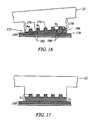
- FIG. 16is a detailed view of one embodiment of the template shown in FIGS. 1, 3 , 11 , 12 , 13 , 14 and 15 in superimposition with a substrate;
- FIG. 17is a detailed view of the template shown in FIG. 16 showing a desired spatial arrangement with respect to the substrate.
- an orientation stage 10is shown having an inner frame 12 disposed proximate to an outer frame 14 , a flexure ring 16 and a compliant device 18 .
- Compliant device 18is discussed more fully below.
- a template chuck 20is coupled to orientation stage 10 , shown more clearly in FIG. 2 .
- template chuck 20is coupled to compliant device 18 .
- Template chuck 20is configured to support a template 22 , shown in FIG. 1 .
- An exemplary template chuckis disclosed in U.S. patent publication No. 2004/0090611 entitled “Chuck System for Modulating Shapes of Substrate,” assigned to the assignee of the present invention and is incorporated by reference herein.
- inner frame 12has a central throughway 24
- outer frame 14has a central opening 26 in superimposition with central throughway 24
- Flexure ring 16has an annular shape, e.g. circular or elliptical and is coupled to inner frame 12 and outer frame 14 and lies outside of both central throughway 24 and central opening 26 .
- flexure ring 16is coupled to inner frame 12 at regions 28 , 30 , and 32 and outer frame 14 at regions 34 , 36 , and 38 .
- Region 34is disposed between regions 28 and 30 and disposed equidistant therefrom; region 36 is disposed between regions 30 and 32 and disposed equidistant therefrom; and region 38 is disposed between regions 28 and 32 and disposed equidistant therefrom.
- flexure ring 16surrounds compliant device 18 , template chuck 20 , and template 22 and fixedly attaches inner frame 12 to outer frame 14 .
- Orientation stage 10is configured to control movement of template 22 and place the same in a desired spatial relationship with respect to a reference surface (not shown).
- plurality of actuators 40 , 42 , and 44are connected between outer frame 14 and inner frame 12 so as to be spaced about orientation stage 10 .
- Each of actuators 40 , 42 , and 44has a first end 46 and a second end 48 .
- First end 46 of actuator 40faces outer frame 14
- second end 48faces inner frame 12 .
- Actuators 40 , 42 , and 44tilt inner frame 12 with respect to outer frame 14 by facilitating translational motion of inner frame 12 along three axes Z 1 , Z 2 , and Z 3 .
- Orientation stage 10may provide a range of motion of approximately ⁇ 1.2 mm about axes Z 1 , Z 2 , and Z 3 .
- actuators 40 , 42 , and 44cause inner frame 12 to impart angular motion to both compliant device 18 and, therefore, template 22 and template chuck 20 , angular motion about one or more of a plurality of axes T 1 , T 2 and T 3 .
- angular motion about tilt axis T 2occurs in a first direction.
- angular motion about tilt axis T 2occurs in a second direction opposite to the first direction.
- angular movement about axis T 1may occur by varying the distance between inner frame 12 and outer frame 14 by movement of inner frame 12 along axes Z 1 and Z 2 in the same direction and magnitude while moving of the inner frame 12 along axis Z 3 in a direction opposite and twice to the movement along axes Z 1 and Z 2 .
- angular movement about axis T 3may occur by varying the distance between inner frame 12 and outer frame 14 by movement of inner frame 12 along axes Z 1 and Z 3 in the same direction and magnitude while moving of inner frame 12 along axis Z 2 in direction opposite and twice to the movement along axes Z 1 and Z 3 .
- Actuators 40 , 42 , and 44may have a maximum operational force of ⁇ 200 N.
- Orientation stage 10may have a may provide a range of motion of approximately ⁇ 0.15° about axes T 1 , T 2 , and T 3 .
- Actuators 40 , 42 , and 44are selected to minimize mechanical parts and, therefore, minimize uneven mechanical compliance, as well as friction, which may cause particulates.
- Examples of actuators 40 , 42 , and 44include voice coil actuators, piezo actuators, and linear actuators.
- An exemplary embodiment for actuators 40 , 42 , and 44is available from BEI Technologies of Sylmar, Calif. under the trade name LA24-20-000A.
- actuators 40 , 42 , and 44are coupled between inner frame 12 and outer frame 14 so as to be symmetrical disposed thereabout and lie outside of central throughway 24 and central opening 26 . With this configuration an unobstructed throughway between outer frame 14 to compliant device 18 is configured. Additionally, the symmetrical arrangement minimizes dynamic vibration and uneven thermal drift, thereby providing fine-motion correction of inner frame 12 .
- the combination of the inner frame 12 , outer frame 14 , flexure ring 16 and actuators 40 , 42 , and 44provides angular motion of compliant device 18 and, therefore, template chuck 20 and template 22 about tilt axes T 1 , T 2 and T 3 . It is desired, however, that translational motion be imparted to template 22 along axes that lie in a plane extending transversely, if not orthogonally, to axes Z 1 , Z 2 , and Z 3 .
- compliant device 18with a functionality to impart angular motion upon template 22 about one or more of a plurality of compliance axes, shown as C 1 and C 2 , which are spaced-part from tilt axes T 1 , T 2 and T 3 and exist on the surface of the template when the template, the template chuck, and the compliant device are assembled.
- compliant device 18includes a support body 50 and a floating body 52 that is coupled to the support body 50 vis-à-vis a plurality of flexure arms 54 , 56 , 58 , and 60 .
- Template chuck 20is intended to be mounted to floating body 52 via conventional fastening means, and template 22 is retained by chuck using conventional methods.
- Each of flexure arms 54 , 56 , 58 , and 60includes first and second sets of flexure joints 62 , 64 , 66 , and 68 .
- the first and second sets of flexure joints 62 , 64 , 66 , and 68are discussed with respect to flexure arm 56 for ease of discussion, but this discussion applies equally to the sets of flexure joints associated with flexure arms 56 , 58 , and 60 .
- compliant device 18is formed from a solid body, for example, stainless steel.
- support body 50 , floating body 52 and flexures arms 54 , 56 , 58 , and 60are integrally formed, are rotationally coupled together vis-à-vis first and second sets of flexure joints 62 , 64 , 66 , and 68 .
- Support body 50includes a centrally disposed throughway 70 .
- Floating bodyincludes a centrally disposed aperture 72 that is in superimposition with throughway 70 .
- Each flexure arm 54 , 56 , 58 , and 60includes opposed ends, 74 and 76 .
- End 74 of each flexure arms 54 , 56 , 58 , and 60is connected to support body 50 through flexure joints 66 and 68 .
- End 74lies outside of throughway 70 .
- End 76 of each flexure arm 54 , 56 , 58 , and 60is connected to floating body 52 through flexure joints 62 and 64 .
- End 76lies outside of aperture 72 .
- each of joints 62 , 64 , 66 , and 68are formed by reducing material from device 18 proximate to ends 74 and 76 , i.e., at an interface either of support body 50 or floating body 52 and one of flexure arms 54 , 56 , 58 , and 60 .
- flexure joints 62 , 64 , 66 , and 68are formed by machining, laser cutting or other suitable processing of device 18 .
- joints 62 , 64 , 66 , and 68are formed from a flexure member 78 having two opposing surfaces 80 and 82 .
- Each of surfaces 80 and 82includes a hiatus 84 and 86 .
- Hiatus 84is positioned facing away from hiatus 86 , and hiatus 86 faces away from hiatus 84 . Extending from hiatus 86 , away from surface 80 is a gap 88 , terminating in an opening in a periphery of flexure arm 56 .
- Joint 68is also formed from a flexure member 90 having two opposing surfaces 92 and 94 . Each of surfaces 92 and 94 includes a hiatus 96 and 98 , respectively.
- Hiatus 98is positioned facing surface 92 , and hiatus 98 faces away from surface 94 .
- gaps 88 , 100 , and 102Extending from hiatus 98 , away from surface 92 is a gap 100 , and extending from hiatus 98 is a gap 102 .
- the spacing S 1 , S 2 and S 3 of gaps 88 , 100 , and 102respectively define a range of motion over which relative movement between either of support body 50 and floating body 52 may occur.
- flexure member 78 associated with joints 62 of flexure arms 56 and 58facilitates rotation about axis 136
- flexure member 78 associated with joints 66 of flexure arms 56 and 58facilitates rotation about axis 138
- Flexure member 78 associated with joints 62 of flexure arms 54 and 60facilitates rotation about axis 108
- flexure member 78 associated with joints 66 of flexure arms 54 and 60facilitates rotation about axis 110
- Flexure member 78 associated with joints 64 of flexure arms 54 and 56facilitates rotation about axis 112
- flexure member 90 associated with joints 68 of flexure arms 54 and 56facilitates rotation about axis 114
- Flexure member 78 associated with joints 64 of flexure arms 58 and 60facilitates rotation about axis 116
- flexure member 90 associated with joints 68 of flexure arms 58 and 60facilitates rotation about axis 118 .
- each flexure arm 54 , 56 , 58 , and 60is located at a region of said device 18 where groups of the axes of rotation overlap.
- end 74 of flexure arm 54is located where axes 72 and 76 overlap and end 76 is positioned where axes 74 and 78 overlap.
- End 74 of flexure arm 56is located where axes 68 and 76 overlap, and end 76 is positioned where axes 70 and 78 overlap.
- End 74 of flexure arm 58is located where axes 68 and 80 overlap, and end 76 is located where axes 70 and 82 overlap.
- end 74 of flexure arm 60is located where axes 72 and 80 overlap, and end 76 is located where 82 and 74 overlap.
- each flexure arm 54 , 56 , 58 , and 60is coupled to provide relative rotational movement with respect to support body 50 and floating body 52 about two groups of overlapping axes with a first group extending transversely to the remaining group.
- Thisprovides each of flexure arms 54 , 56 , 58 , and 60 with movement about two groups of orthogonal axes while minimizing the footprint of the same.
- Device 18may provide a tilting motion range of approximately ⁇ 0.04°, an active tilting motion range of approximately ⁇ 0.02°, and an active theta motion range of approximately ⁇ 0.0005° above the above mentioned axes.
- each flexure arm 54 , 56 , 58 , and 60allows leaving a void 120 between throughway 70 and aperture 72 unobstructed by flexure arms 54 , 56 , 58 , and 60 .
- each flexures arms 54 , 56 , 58 , and 60with respect to support body 50 and floating body 52 facilitates parallel transfer of loads in device 18 .
- each flexures arms 54 , 56 , 58 , and 60imparts an substantially equal amount of force F 1 upon floating body 52 .
- thisfacilitates obtaining a desired structural stiffness with device 18 when load with either a force F 1 or a force F 2 .
- joints are 62 , 64 , 66 , and 68are revolute joints which minimize movement, in all directions, between the flexure are and either support body 50 or floating body 52 excepting rotational movement.
- joints 62 , 64 , 66 , and 68minimize translational movement between flexure arms 54 , 56 , 58 , and 60 , support body 50 and floating body 52 , while facilitating rotational movement about axes 104 , 106 , 108 , 110 , 112 , 114 , 116 , and 118 .
- the relative position of axes 104 , 106 , 108 , and 110provides floating body 52 with a first remote of compliance (RCC) at a position 122 spaced apart from floating body 52 , centered with respect to aperture 72 and equidistant from each axis 104 , 106 , 108 , and 110 .
- RCCremote of compliance
- the relative position of axes 112 , 114 , 116 , and 118provides floating body 52 with a second RCC substantially close to position 122 and desirably located at position 122 .
- Each axis 112 , 114 , 116 , and 118is positioned equidistant from position 122 .
- Each axis of the group of axes 104 , 106 , 108 , and 110extends parallel to the remaining axes 104 , 106 , 108 , and 110 of the group.
- each axis of the group of axes 104 , 106 , 108 , and 110extends parallel to the remaining axes 104 , 106 , 108 , and 110 of the group and orthogonally to each axis 104 , 106 , 108 , and 110 .
- Axis 110is spaced-apart from axis 108 along a first direction a distance d 1 and along a second orthogonal direction a distance d 2 .
- Axis 104is spaced-apart from axis 106 along the first direction a distance d 3 and along the second direction a distance d 4 .
- Axis 112is spaced-apart from axis 114 along a third direction, that is orthogonal to both the first and second directions a distance d 5 and along the second direction a distance d 6 .
- Axis 116is spaced-apart from axis 118 along the second direction a distance d 7 and along the third direction a distance d 8 .
- Distances d 1 , d 4 , d 6 and d 7are substantially equal.
- Distances d 2 , d 3 , d 5 and d 8are substantially equal.
- Two sets of transversely extending axesmay be in substantially close proximity such that RCC 122 may be considered to lie upon an intersection thereat by appropriately establishing distances d 1 -d 8 .
- a first set ofincludes four axes is shown as 124 , 126 , 128 , and 130 .
- Joints 62 and 66 of flexure arm 54lie along axis 124
- joints 62 and 66 of flexure arm 54lie along axis 126 .
- Joints 62 and 66 of flexure arm 58lie along axis 128
- joints 62 and 66 of flexure arm 60lie along axis 130 .
- a second set of four axesis shown as 132 , 134 , 136 , and 138 .
- Joints 64 and 68 of flexure arm 56lie along axis 132
- joints 64 and 68 of flexure arm 58lie along axis 134
- Joints 64 and 68 of flexure arm 60lie along axis 136
- joints 64 and 68 of flexure arm 54lie along axis 138 .
- Thisprovides a gimbal-like movement of floating body 52 with respect to RCC 122 .
- RCC 122With the structural stiffness to resist, if not prevent, translational movement of floating body with respect to axis 124 , 126 , 128 , 130 , 132 , 134 , 136 , and 138 .
- device 18may be provided with active compliance functionality shown with device 18 .
- a plurality of lever arms 140 , 142 , 146 , and 148are coupled to floating body 52 and extend toward support body 50 terminating proximate to a piston of an actuator.
- lever arm 140has one end positioned proximate to the piston of actuator 150
- lever arm 142has one end positioned proximate to the piston of actuator 152
- lever arm 146has one end positioned proximate to the piston of actuator 154
- one end of actuator arm 118is positioned proximate to the piston of actuator 156 that is coupled thereto.
- actuators 150 , 152 , 154 , and 156By activating the proper sets of actuators 150 , 152 , 154 , and 156 , angular positioning of the relative position of floating body 52 with respect to support body 50 may be achieved.
- An exemplary embodiment for actuators 150 , 152 , 154 , and 156is available from BEI Technologies of Sylmar, Calif. under the trade name LA10-12-027A.
- actuators 150 , 152 , 154 , and 156may be activated.
- actuator 150may be activated to move lever arm 140 along the F 1 direction and actuator 154 would be operated to move lever arm 146 in a direction opposite to the direction lever arm 140 moves.
- actuators 152 and 156are activated to move lever arms 142 and 148 respectively.
- each of lever arms 140 , 142 , 146 , and 148are moved toward one of flexure arms 54 , 56 , 58 , and 60 that differs from the flexure arm 54 , 56 , 58 , and 60 toward which the remaining lever arms 140 , 142 , 146 , and 148 move.
- An examplemay include moving lever arm 140 toward flexure arm 54 , lever arm 142 toward flexure arm 56 , lever arm 146 toward flexure arm 58 and lever arm 142 toward flexure arm 60 . This would impart rotational movement about the F 3 direction.
- each of lever arms 140 , 142 , 146 , and 148may be moved in the opposite direction. Were it desired to prevent translational displacement between support body 50 and floating body 52 along the F 3 direction while imparting rotational movement thereabout, then each of lever arms 140 , 142 , 146 , and 148 would be moved the same magnitude. However, were it desired to impart rotational movement of floating body 52 about the F 1 and F 2 directions, this may be achieved in various manners.
- floating body 52can be actively adjusted for two independent angular configuration with respect to support body by translation along the F 3 direction. For example, moving each of lever arms 140 , 142 , 146 , and 148 with actuators 150 , 152 , 154 , and 156 , respectively, differing amounts would impart translation of floating body 52 along the F 3 direction while imparting angular displacement about the F 3 direction. Additionally, moving only three lever arms 140 , 142 , 146 , and 148 would also impart translation motion about the F 3 direction while imparting angular displacement about the F 3 direction.
- two of actuators 150 , 152 , 154 , and 156would be activated to move two of lever arms 140 , 142 , 146 , and 148 .
- two opposing lever armssuch as for example, 140 and 146 , or 142 and 148 would be moved in the same direction the same magnitude.
- orientation stage 10is typically employed with an imprint lithography system (not shown).
- An exemplary lithographic systemis available under the trade name IMPRIO 100TM from Molecular Imprints, Inc. having a place of business at 1807-C Braker Lane, Suite 100, Austin, Tex. 78758.
- the system description for the IMPRIO 100TMis available at www.molecularimprints.com and is incorporated herein by reference.
- orientation stage 10may be employed to facilitate alignment of template 22 with a surface in superimposition therewith, such as a surface of substrate 158 .
- the surface of substrate 158may comprising of the material from which substrate 158 is formed, e.g. silicon with a native oxide present, or may consist of a patterned or unpatterned layer of, for example, conductive material, dielectric material and the like.
- Template 22 and substrate 158are shown spaced-apart a distance defining a gap 160 therebetween.
- the volume associated with gap 160is dependent upon many factors, including the topography of the surface of template 22 facing substrate and the surface of substrate 158 facing template 22 , as well as the angular relationship between a neutral axis A of substrate with respect to the neutral axis B of substrate 158 .
- the volume associated with gap 160would also be dependent upon the angular relation between template 22 and substrate 158 about axis Z.
- template 22includes template alignment marks, one of which is shown as 162
- substrate 158includes substrate alignment marks, one of which is shown as 164 .
- desired alignment between template 22 and substrate 158occurs upon template alignment mark 162 being in superimposition with substrate alignment mark 164 .
- desired alignment between template 22 and substrate 158has not occurred, shown by the two marks be offset, a distance O.
- offset Ois shown as being a linear offset in one direction, it should be understood that the offset may be linear along two direction shown as O 1 and O 2 .
- the offset between template 22 and substrate 158may also consist of an angular offset, shown in FIG. 13 as angle ⁇ .
- desired alignment between template 22 and substrate 158is obtained by the combined rotational movement about one or more axes T 1 , T 2 , T 3 , F 1 , F 2 and F 3 .
- template chuck 20 and template 22 about one or more axes T 1 , T 2 , T 3is undertaken. This typically results in an oblique angle ⁇ being produced between neutral axes A and B.
- angular movement of template 22 about one or more of axes F 1 and F 2are undertaken to compensate for the angle ⁇ and ensure that neutral axis A extends parallel to neutral axis B.
- template 22may be properly aligned with respect to substrate 158 along to linear axes lying in a plane extending parallel to neutral axis B, shown in FIG. 15 .
- template 22would be rotated about axis F 3 by use of actuators 150 , 152 , 154 , and 156 to provide the desired alignment.
- actuators 40 , 42 , and 44are operated to move template 22 into contact with a surface proximate to substrate.
- surfaceconsists of polymerizable imprinting material 166 disposed on substrate 158 . It should be noted that actuators 40 , 42 , and 44 are operated to minimize changes in the angle formed between neutral axes A and B once desired alignment has been obtained.
- neutral axes A and Bit should be known, however, that it is not necessary for neutral axes A and B to extend exactly parallel to one another, so long as the angular deviation from parallelism is within the compliance tolerance of compliant device 18 , as defined by flexure joints 62 , 64 , 66 , and 68 and flexure arms 54 , 56 , 58 , and 60 . In this fashion, neutral axes A and B may be orientated to be as parallel as possible in order to maximize the resolution of pattern formation into polymerizable material. As a result, it is desired that position 122 at which the first and second RCCs are situation be placed at the interface of template 22 and material.
- template 22typically includes a mesa 170 having a pattern recorded in a surface thereof, defining a mold 172 .
- An exemplary template 22is shown in U.S. Pat. No. 6,696,220, which is incorporated by reference herein.
- the patterned on mold 172may comprising of a smooth surface of a plurality of features, as shown, formed by a plurality of spaced-apart recesses 174 and projections 176 .
- Projections 30have a width W 1
- recesses 28have a width W 2 .
- the plurality of featuresdefines an original pattern that forms the basis of a pattern to be transferred into a substrate 158 .
- the pattern recorded in material 166is produced, in part, by mechanical contact of the material 166 with mold 172 and substrate 158 , which as shown, may include an existing layer thereon, such as a transfer layer 178 .
- An exemplary embodiment for transfer layer 178is available from Brewer Science, Inc. of Rolla, Mo. under the trade name DUV30J-6. It should be understood that material 166 and transfer layer 178 may be deposited using any known technique, including drop dispense and spin-coating techniques.
- Thickness t 1is referred to as a residual thickness. Thicknesses “t 1 ” and “t 2 ” may be any thickness desired, dependent upon the application. Thickness t 1 and t 2 may have a value in the range of 10 nm to 10 ⁇ m.
- the total volume contained material 166may be such so as to minimize, or to avoid, a quantity of material 166 from extending beyond the region of substrate 158 not in superimposition with mold 172 , while obtaining desired thicknesses t 1 and t 2 .
- mesa 170is provided with a height, h m , which is substantially greater than a depth of recesses 174 , h r .
- h ma height of recesses 174 , h r .
- a benefit provided by system 10is that it facilitates precise control over thicknesses t 1 and t 2 .
- thicknesses t 1are not uniform, as neither are thickness t 2 . This is an undesirable orientation of mold 172 with respect to substrate 158 .
- uniform thickness t 1 and t 2may be obtained, shown in FIG. 17 .
- precise control over thickness t 1 and t 2may be obtained, which is highly desirable.
- system 10provide a three sigma alignment accuracy having a minimum feature size of, for example, about 50 nm or less.
Landscapes
- Engineering & Computer Science (AREA)
- Nanotechnology (AREA)
- Chemical & Material Sciences (AREA)
- Physics & Mathematics (AREA)
- Crystallography & Structural Chemistry (AREA)
- General Physics & Mathematics (AREA)
- Mechanical Engineering (AREA)
- Mathematical Physics (AREA)
- Theoretical Computer Science (AREA)
- Condensed Matter Physics & Semiconductors (AREA)
- Manufacturing & Machinery (AREA)
- Exposure Of Semiconductors, Excluding Electron Or Ion Beam Exposure (AREA)
- Container, Conveyance, Adherence, Positioning, Of Wafer (AREA)
- Shaping Of Tube Ends By Bending Or Straightening (AREA)
- Physical Or Chemical Processes And Apparatus (AREA)
- Biological Treatment Of Waste Water (AREA)
- Manipulator (AREA)
- Manufacture, Treatment Of Glass Fibers (AREA)
- Transmission Devices (AREA)
Abstract
Description
- The field of invention relates generally to remote center compliant devices. More particularly, the present invention is directed to a compliant device suited for use in imprint lithography to hold a template.
- Compliant devices are devices that have elastic properties to compliantly float one body relative to another, while providing a desired number of degrees of freedom of movement therebetween. These properties permit, inter alia, the floating body to compensate out-of-tolerance spatial orientations with respect to a work surface. Active compliant devices use actuators to achieve a desired spatial orientation between bodies. “Passive” compliant devices are unpowered, i.e., with out active control. Being able to be kinematically constrained in any translational or rotational direction, a “passive” compliant device achieves proper spatial orientation between the floating body and a work piece through interconnecting linkages and passive elastic elements, e.g., springs. Actuation of the compliance function occurs upon contact of the floating body with the work surface. To that end, forces transferred between the floating body and a support body coupled thereto via linkages may be achieved serially or in parallel.
- An exemplary compliant device is shown in U.S. Pat. No. 6,696,220 to Bailey et al. that discloses a remote passive compliant device for use in imprint lithography. The remote passive compliant device facilitates a transfer of forces between the floating body and a support body coupled thereto serially, through a plurality of linkages. The linkages are coupled between the floating body and the support by via flexure joints. With this configuration, proper spatial orientation between an imprint lithography template and imprinting material of a work surface may be achieved.
- Thus, a need exists for providing improved compliant devices for use in imprint lithography processes.
- The present invention is directed to a compliant device comprising a support body, a floating body, and a plurality of flexure arms. Each of the plurality of transfer arms is connected between the support body and the floating body to transfer a load therebetween in parallel. To that end, the flexure arms having first and second sets of flexure joints. The first set of flexure joints facilitate rotational movement of the flexure arm about a first axis extending along a first direction. The second set of flexure joints arranged to facilitate rotational movement of the flexure arm about a second axis, extending along a second direction that is transverse to the first direction. The flexure joints are revolute joints. Thus, the movement of the flexure arms is constrained to rotational movement about two transversely orientated axes. In one embodiment the compliant device is a passive compliant device. In an alternate embodiment, the compliant device is an active compliant device. These and other embodiments are discussed more fully below.
- The present invention is directed towards a method and system of controlling movement of a body coupled to an actuation system that features translating movement of the body in a plane extending by imparting angular motion in the actuation system with respect to two spaced-apart axes. Specifically, rotational motion is generated in two spaced-apart planes, one of which extending parallel to the plane in which the body translates. This facilitates proper orientation of body with respect to a surface spaced-apart therefrom. These and other embodiments are discussed more fully below.
FIG. 1 is an exploded perspective view of an orientation stage showing a template chuck and a template in accordance with the present invention;FIG. 2 is perspective view of the orientation stage shown inFIG. 1 ;FIG. 3 is an exploded perspective view of a passive compliant device included in the orientation stage shown inFIG. 1 along with the template holder and the template in accordance with a first embodiment of the present invention;FIG. 4 is a detailed perspective view of the passive compliant device shown inFIG. 3 ;FIG. 5 is a side view of the passive compliant, device shown inFIG. 4 , showing detail of flexure joints included therewith;FIG. 6 is a side view of the passive compliant device shown inFIG. 4 ;FIG. 7 is a side view of the compliant device, shown inFIG. 6 , rotated 90 degrees;FIG. 8 is a side view of the compliant device, shown inFIG. 6 , rotated 180 degrees;FIG. 9 is a side view of the compliant device, shown inFIG. 6 , rotated 270 degrees; andFIG. 10 is a perspective view of a compliant device in accordance with an alternate embodiment of the present invention;FIG. 11 is a simplified elevation view of a the template, shown inFIG. 1 , in superimposition with a substrate showing misalignment along one direction;FIG. 12 is a top down view of the template and substrate, shown inFIG. 11 , showing misalignment along two transverse direction;FIG. 13 . is a top down view of the template and substrate, shown inFIG. 11 , showing angular misalignment;FIG. 14 is a simplified elevation view of the template, shown inFIG. 1 , in superimposition with a substrate showing angular misalignment;FIG. 15 is a simplified elevation view showing desired alignment between the template and substrate shown inFIGS. 11, 12 ,13 and14;FIG. 16 is a detailed view of one embodiment of the template shown inFIGS. 1, 3 ,11,12,13,14 and15 in superimposition with a substrate; andFIG. 17 is a detailed view of the template shown inFIG. 16 showing a desired spatial arrangement with respect to the substrate.- Referring to
FIG. 1 , anorientation stage 10 is shown having aninner frame 12 disposed proximate to anouter frame 14, aflexure ring 16 and acompliant device 18.Compliant device 18 is discussed more fully below. Atemplate chuck 20 is coupled toorientation stage 10, shown more clearly inFIG. 2 . Specifically,template chuck 20 is coupled tocompliant device 18.Template chuck 20 is configured to support atemplate 22, shown inFIG. 1 . An exemplary template chuck is disclosed in U.S. patent publication No. 2004/0090611 entitled “Chuck System for Modulating Shapes of Substrate,” assigned to the assignee of the present invention and is incorporated by reference herein. - Referring to
FIGS. 1 and 2 ,inner frame 12 has acentral throughway 24, andouter frame 14 has acentral opening 26 in superimposition withcentral throughway 24.Flexure ring 16 has an annular shape, e.g. circular or elliptical and is coupled toinner frame 12 andouter frame 14 and lies outside of bothcentral throughway 24 andcentral opening 26. Specifically,flexure ring 16 is coupled toinner frame 12 atregions outer frame 14 atregions Region 34 is disposed betweenregions region 36 is disposed betweenregions regions flexure ring 16 surroundscompliant device 18,template chuck 20, andtemplate 22 and fixedly attachesinner frame 12 toouter frame 14. Orientation stage 10 is configured to control movement oftemplate 22 and place the same in a desired spatial relationship with respect to a reference surface (not shown). To that end, plurality ofactuators outer frame 14 andinner frame 12 so as to be spaced aboutorientation stage 10. Each ofactuators first end 46 and asecond end 48. First end46 ofactuator 40 facesouter frame 14, andsecond end 48 facesinner frame 12.Actuators inner frame 12 with respect toouter frame 14 by facilitating translational motion ofinner frame 12 along three axes Z1, Z2, and Z3.Orientation stage 10 may provide a range of motion of approximately ±1.2 mm about axes Z1, Z2, and Z3. In this fashion,actuators inner frame 12 to impart angular motion to bothcompliant device 18 and, therefore,template 22 andtemplate chuck 20, angular motion about one or more of a plurality of axes T1, T2and T3. Specifically, by decreasing a distance betweeninner frame 12 andouter frame 14 along axes Z2and Z3and increasing a distance therebetween along axis Z1, angular motion about tilt axis T2occurs in a first direction. Increasing the distance betweeninner frame 12 andouter frame 14 along axes Z2and Z3and decreasing the distance therebetween along axis Z1, angular motion about tilt axis T2occurs in a second direction opposite to the first direction. In a similar manner angular movement about axis T1may occur by varying the distance betweeninner frame 12 andouter frame 14 by movement ofinner frame 12 along axes Z1and Z2in the same direction and magnitude while moving of theinner frame 12 along axis Z3in a direction opposite and twice to the movement along axes Z1and Z2. Similarly, angular movement about axis T3may occur by varying the distance betweeninner frame 12 andouter frame 14 by movement ofinner frame 12 along axes Z1and Z3in the same direction and magnitude while moving ofinner frame 12 along axis Z2in direction opposite and twice to the movement along axes Z1and Z3.Actuators N. Orientation stage 10 may have a may provide a range of motion of approximately ±0.15° about axes T1, T2, and T3.Actuators actuators actuators inner frame 12 andouter frame 14 so as to be symmetrical disposed thereabout and lie outside ofcentral throughway 24 andcentral opening 26. With this configuration an unobstructed throughway betweenouter frame 14 tocompliant device 18 is configured. Additionally, the symmetrical arrangement minimizes dynamic vibration and uneven thermal drift, thereby providing fine-motion correction ofinner frame 12.- The combination of the
inner frame 12,outer frame 14,flexure ring 16 andactuators compliant device 18 and, therefore,template chuck 20 andtemplate 22 about tilt axes T1, T2and T3. It is desired, however, that translational motion be imparted totemplate 22 along axes that lie in a plane extending transversely, if not orthogonally, to axes Z1, Z2, and Z3. This is achieved by providingcompliant device 18 with a functionality to impart angular motion upontemplate 22 about one or more of a plurality of compliance axes, shown as C1and C2, which are spaced-part from tilt axes T1, T2and T3and exist on the surface of the template when the template, the template chuck, and the compliant device are assembled. - Referring to
FIGS. 3 and 4 ,compliant device 18 includes asupport body 50 and a floatingbody 52 that is coupled to thesupport body 50 vis-à-vis a plurality offlexure arms Template chuck 20 is intended to be mounted to floatingbody 52 via conventional fastening means, andtemplate 22 is retained by chuck using conventional methods. - Each of
flexure arms flexure joints flexure joints flexure arm 56 for ease of discussion, but this discussion applies equally to the sets of flexure joints associated withflexure arms compliant device 18 is formed from a solid body, for example, stainless steel. As a result,support body 50, floatingbody 52 andflexures arms flexure joints Support body 50 includes a centrally disposedthroughway 70. Floating body includes a centrally disposedaperture 72 that is in superimposition withthroughway 70. Eachflexure arm End 74 of eachflexure arms body 50 throughflexure joints End 74 lies outside ofthroughway 70.End 76 of eachflexure arm body 52 throughflexure joints End 76 lies outside ofaperture 72. - Referring to
FIGS. 4 and 5 , each ofjoints device 18 proximate to ends74 and76, i.e., at an interface either ofsupport body 50 or floatingbody 52 and one offlexure arms device 18. Specifically, joints62,64,66, and68 are formed from aflexure member 78 having two opposingsurfaces surfaces hiatus Hiatus 84 is positioned facing away fromhiatus 86, andhiatus 86 faces away fromhiatus 84. Extending fromhiatus 86, away fromsurface 80 is agap 88, terminating in an opening in a periphery offlexure arm 56. Joint68 is also formed from aflexure member 90 having two opposingsurfaces surfaces hiatus Hiatus 98 is positioned facingsurface 92, andhiatus 98 faces away fromsurface 94. Extending fromhiatus 98, away fromsurface 92 is agap 100, and extending fromhiatus 98 is agap 102. The spacing S1, S2 and S3 ofgaps support body 50 and floatingbody 52 may occur. - Referring to
FIGS. 3 and 5 ,flexure member 78 associated withjoints 62 offlexure arms axis 136, andflexure member 78 associated withjoints 66 offlexure arms axis 138.Flexure member 78 associated withjoints 62 offlexure arms axis 108, andflexure member 78 associated withjoints 66 offlexure arms axis 110.Flexure member 78 associated withjoints 64 offlexure arms axis 112, andflexure member 90 associated withjoints 68 offlexure arms axis 114.Flexure member 78 associated withjoints 64 offlexure arms axis 116, andflexure member 90 associated withjoints 68 offlexure arms axis 118. - As a result, each
flexure arm device 18 where groups of the axes of rotation overlap. For example, end74 offlexure arm 54 is located where axes72 and76 overlap and end76 is positioned where axes74 and78 overlap.End 74 offlexure arm 56 is located where axes68 and76 overlap, and end76 is positioned where axes70 and78 overlap.End 74 offlexure arm 58 is located where axes68 and80 overlap, and end76 is located where axes70 and82 overlap. Similarly, end74 offlexure arm 60 is located where axes72 and80 overlap, and end76 is located where82 and74 overlap. - As a result of this configuration, each
flexure arm body 50 and floatingbody 52 about two groups of overlapping axes with a first group extending transversely to the remaining group. This provides each offlexure arms Device 18 may provide a tilting motion range of approximately ±0.04°, an active tilting motion range of approximately ±0.02°, and an active theta motion range of approximately ±0.0005° above the above mentioned axes. Furthermore, having the reduced footprint of eachflexure arm throughway 70 andaperture 72 unobstructed byflexure arms device 18 suited for use with an imprint lithography system, discussed more fully below. - Referring to
FIGS. 4, 6 and7, the present configuration offlexure arms body 50 and floatingbody 52 facilitates parallel transfer of loads indevice 18. For example, were a load force imparted uponsupport body 50, eachflexures arms body 52. Among other things, this facilitates obtaining a desired structural stiffness withdevice 18 when load with either a force F1or a force F2. To that end, joints are62,64,66, and68 are revolute joints which minimize movement, in all directions, between the flexure are and eithersupport body 50 or floatingbody 52 excepting rotational movement. Specifically, joints62,64,66, and68 minimize translational movement betweenflexure arms support body 50 and floatingbody 52, while facilitating rotational movement aboutaxes - Referring to
FIGS. 4, 5 ,6, and7, the relative position ofaxes body 52 with a first remote of compliance (RCC) at aposition 122 spaced apart from floatingbody 52, centered with respect toaperture 72 and equidistant from eachaxis axes body 52 with a second RCC substantially close toposition 122 and desirably located atposition 122. Eachaxis position 122. Each axis of the group ofaxes axes axes axes axis Axis 110 is spaced-apart fromaxis 108 along a first direction a distance d1and along a second orthogonal direction a distance d2.Axis 104 is spaced-apart fromaxis 106 along the first direction a distance d3and along the second direction a distance d4.Axis 112 is spaced-apart fromaxis 114 along a third direction, that is orthogonal to both the first and second directions a distance d5and along the second direction a distance d6.Axis 116 is spaced-apart fromaxis 118 along the second direction a distance d7 and along the third direction a distance d8. Distances d1, d4, d6and d7are substantially equal. Distances d2, d3, d5and d8are substantially equal. - Two sets of transversely extending axes may be in substantially close proximity such that
RCC 122 may be considered to lie upon an intersection thereat by appropriately establishing distances d1-d8. A first set of includes four axes is shown as124,126,128, and130.Joints flexure arm 54 lie alongaxis 124, and joints62 and66 offlexure arm 54 lie alongaxis 126.Joints flexure arm 58 lie alongaxis 128, and joints62 and66 offlexure arm 60 lie alongaxis 130. A second set of four axes is shown as132,134,136, and138.Joints flexure arm 56 lie alongaxis 132, and joints64 and68 offlexure arm 58 lie alongaxis 134.Joints flexure arm 60 lie alongaxis 136, and joints64 and68 offlexure arm 54 lie alongaxis 138. With this configuration movement of floatingbody 52, with respect toRCC 122, about any one of the set ofaxes axes body 52 with respect toRCC 122. With the structural stiffness to resist, if not prevent, translational movement of floating body with respect toaxis - Referring to
FIGS. 4 and 10 , in accordance with an alternate embodiment of the present invention,device 18 may be provided with active compliance functionality shown withdevice 18. To that end, a plurality oflever arms body 52 and extend towardsupport body 50 terminating proximate to a piston of an actuator. As shownlever arm 140 has one end positioned proximate to the piston ofactuator 150,lever arm 142 has one end positioned proximate to the piston ofactuator 152, lever arm146 has one end positioned proximate to the piston ofactuator 154 and one end ofactuator arm 118 is positioned proximate to the piston ofactuator 156 that is coupled thereto. By activating the proper sets ofactuators body 52 with respect to supportbody 50 may be achieved. An exemplary embodiment foractuators - To provide rotational movement of floating
body 52 with respect to supportbody 50actuators actuator 150 may be activated to movelever arm 140 along the F1direction andactuator 154 would be operated to move lever arm146 in a direction opposite to thedirection lever arm 140 moves. Similarly, at least one ofactuators lever arms actuators lever arms flexure arms flexure arm lever arms lever arm 140 towardflexure arm 54,lever arm 142 towardflexure arm 56, lever arm146 towardflexure arm 58 andlever arm 142 towardflexure arm 60. This would impart rotational movement about the F3direction. It should be understood, however, each oflever arms support body 50 and floatingbody 52 along the F3direction while imparting rotational movement thereabout, then each oflever arms body 52 about the F1and F2directions, this may be achieved in various manners. - Since rotational movement of floating
body 52 is guided by the first and second RCCs, floatingbody 52 can be actively adjusted for two independent angular configuration with respect to support body by translation along the F3direction. For example, moving each oflever arms actuators body 52 along the F3direction while imparting angular displacement about the F3direction. Additionally, moving only threelever arms support body 50 and floatingbody 52 without impart rotational movement therebetween, two ofactuators lever arms lever arms 140 and146 in one direction, e.g., towardflexure arms body 52 extending betweenflexure arms support body 50 in superimposition therewith, effectively creating rotation movement of floatingbody 16 about the F2direction. Decrease would the distance between the side of floatingbody 52 extending betweenflexure arms support body 50 in superimposition therewith. Conversely, movinglever arms 140 and146 in an opposite direction, e.g., towardflexure arms body 52 extending betweenflexure arms support body 50. The distance between the side of floatingbody 52 extending betweenflexure arms support body 50 in superimposition therewith would increase. Similarly, rotational movement of floatingbody 52 about the F1direction may be achieved by movement oflever arms actuators lever arms 140 and146. It should be understood that any linear combination of movement of the aforementioned lever arms may be effectuated to achieve desired motion. - From the foregoing it is seen that rotational motions of floating
body 52 about the F1, F2and F3directions are orthogonal to each other. By adjusting the magnitude of each actuation force or position atactuators flexure arms body 52 andsupport body 50. - Referring to
FIGS. 1, 11 and12, in operation,orientation stage 10 is typically employed with an imprint lithography system (not shown). An exemplary lithographic system is available under thetrade name IMPRIO 100™ from Molecular Imprints, Inc. having a place of business at 1807-C Braker Lane,Suite 100, Austin, Tex. 78758. The system description for the IMPRIO 100TM is available at www.molecularimprints.com and is incorporated herein by reference. As a result,orientation stage 10 may be employed to facilitate alignment oftemplate 22 with a surface in superimposition therewith, such as a surface ofsubstrate 158. As a result, the surface ofsubstrate 158 may comprising of the material from whichsubstrate 158 is formed, e.g. silicon with a native oxide present, or may consist of a patterned or unpatterned layer of, for example, conductive material, dielectric material and the like. Template 22 andsubstrate 158 are shown spaced-apart a distance defining agap 160 therebetween. The volume associated withgap 160 is dependent upon many factors, including the topography of the surface oftemplate 22 facing substrate and the surface ofsubstrate 158 facingtemplate 22, as well as the angular relationship between a neutral axis A of substrate with respect to the neutral axis B ofsubstrate 158. In addition, were the topography of both of the aforementioned surfaces patterned, the volume associated withgap 160 would also be dependent upon the angular relation betweentemplate 22 andsubstrate 158 about axis Z. Considering that desirable patterning with imprint lithography techniques is, in large part, dependent upon providing the appropriate volume to gap160, it is desirable toaccurate align template 22 andsubstrate 158. To that end,template 22 includes template alignment marks, one of which is shown as162, andsubstrate 158 includes substrate alignment marks, one of which is shown as164.- In the present example it is assumed that desired alignment between
template 22 andsubstrate 158 occurs upontemplate alignment mark 162 being in superimposition withsubstrate alignment mark 164. As shown, desired alignment betweentemplate 22 andsubstrate 158 has not occurred, shown by the two marks be offset, a distance O. Further, although offset O is shown as being a linear offset in one direction, it should be understood that the offset may be linear along two direction shown as O1 and O2. In addition to, or instead of, the aforementioned linear offset in one or two directions, the offset betweentemplate 22 andsubstrate 158 may also consist of an angular offset, shown inFIG. 13 as angle Θ. - Referring to
FIGS. 2, 10 , and14, desired alignment betweentemplate 22 andsubstrate 158 is obtained by the combined rotational movement about one or more axes T1, T2, T3, F1, F2and F3. Specifically, to attenuate offset linear offset, movement, as a unit, ofcompliant device 18,template chuck 20 andtemplate 22 about one or more axes T1, T2, T3is undertaken. This typically results in an oblique angle φ being produced between neutral axes A and B. Thereafter, angular movement oftemplate 22 about one or more of axes F1and F2are undertaken to compensate for the angle φ and ensure that neutral axis A extends parallel to neutral axis B. Furthermore, the combined angular movement about axes T1, T2, T3, F1, F2results in a swinging motion oftemplate 22 to effectuate movement of the same in a plane extending parallel to neutral axis B and transverse, of not orthogonal, to axes Z1, Z2and Z3. In this manner,template 22 may be properly aligned with respect tosubstrate 158 along to linear axes lying in a plane extending parallel to neutral axis B, shown inFIG. 15 . Were it desired to attenuate, of not abrogate, angular offset,template 22 would be rotated about axis F3 by use ofactuators - After the desired alignment has occurred,
actuators template 22 into contact with a surface proximate to substrate. In the present example surface consists ofpolymerizable imprinting material 166 disposed onsubstrate 158. It should be noted thatactuators compliant device 18, as defined byflexure joints flexure arms position 122 at which the first and second RCCs are situation be placed at the interface oftemplate 22 and material. - Referring to
FIGS. 1, 16 and17, as discussed above, the foregoingsystem 10 is useful for patterning substrates, such assubstrate 158 employing imprint lithography techniques. To that end,template 22 typically includes amesa 170 having a pattern recorded in a surface thereof, defining amold 172. Anexemplary template 22 is shown in U.S. Pat. No. 6,696,220, which is incorporated by reference herein. The patterned onmold 172 may comprising of a smooth surface of a plurality of features, as shown, formed by a plurality of spaced-apartrecesses 174 andprojections 176.Projections 30 have a width W1, and recesses28 have a width W2. The plurality of features defines an original pattern that forms the basis of a pattern to be transferred into asubstrate 158. - Referring to
FIGS. 16 and 17 the pattern recorded inmaterial 166 is produced, in part, by mechanical contact of the material166 withmold 172 andsubstrate 158, which as shown, may include an existing layer thereon, such as atransfer layer 178. An exemplary embodiment fortransfer layer 178 is available from Brewer Science, Inc. of Rolla, Mo. under the trade name DUV30J-6. It should be understood thatmaterial 166 andtransfer layer 178 may be deposited using any known technique, including drop dispense and spin-coating techniques. - Upon contact with
material 166, it is desired that portion180 ofmaterial 166 in superimposition withprojections 30 remain having a thickness t1, and sub-portions182 remain having a thickness t2. Thickness t1is referred to as a residual thickness. Thicknesses “t1” and “t2” may be any thickness desired, dependent upon the application. Thickness t1and t2may have a value in the range of 10 nm to 10 μm. The total volume containedmaterial 166 may be such so as to minimize, or to avoid, a quantity ofmaterial 166 from extending beyond the region ofsubstrate 158 not in superimposition withmold 172, while obtaining desired thicknesses t1and t2. To that end,mesa 170 is provided with a height, hm, which is substantially greater than a depth ofrecesses 174, hr. In this manner, capillary forces ofmaterial 166 withsubstrate 158 andmold 172 restrict movement ofmaterial 166 from extending beyond regions ofsubstrate 158 not in superimposition withmold 172, upon t1and t2reaching a desired thickness. - A benefit provided by
system 10 is that it facilitates precise control over thicknesses t1and t2. Specifically, it is desired to have each of thicknesses t1be substantially equal and that each of thicknesses t2be substantially equal. As shown inFIG. 16 , thicknesses t1are not uniform, as neither are thickness t2. This is an undesirable orientation ofmold 172 with respect tosubstrate 158. With thepresent system 10, uniform thickness t1and t2may be obtained, shown inFIG. 17 . As a result, precise control over thickness t1and t2may be obtained, which is highly desirable. In the present invention,system 10 provide a three sigma alignment accuracy having a minimum feature size of, for example, about 50 nm or less. - The embodiments of the present invention described above are exemplary. As a result, many changes and modifications may be made to the disclosure recited above, while remaining within the scope of the invention. Therefore, the scope of the invention should not be limited by the above description, but instead should be determined with reference to the appended claims along with their full scope of equivalents.
Claims (35)
Priority Applications (8)
| Application Number | Priority Date | Filing Date | Title |
|---|---|---|---|
| US10/858,179US20050275311A1 (en) | 2004-06-01 | 2004-06-01 | Compliant device for nano-scale manufacturing |
| EP05755568AEP1766699A4 (en) | 2004-06-01 | 2005-05-27 | Compliant device for nano-scale manufacturing |
| PCT/US2005/018861WO2005119801A2 (en) | 2004-06-01 | 2005-05-27 | Compliant device for nano-scale manufacturing |
| JP2007515425AJP4688871B2 (en) | 2004-06-01 | 2005-05-27 | Compliant devices for nanoscale manufacturing |
| KR1020067027284AKR101127970B1 (en) | 2004-06-01 | 2005-05-27 | Compliant device for nano-scale manufacturing |
| CNA2005800229857ACN101076436A (en) | 2004-06-01 | 2005-05-27 | Compliant device for nano-scale manufacturing |
| US11/142,838US7387508B2 (en) | 2004-06-01 | 2005-06-01 | Compliant device for nano-scale manufacturing |
| TW094117980ATWI288292B (en) | 2004-06-01 | 2005-06-01 | Compliant device for nano-scale manufacturing |
Applications Claiming Priority (1)
| Application Number | Priority Date | Filing Date | Title |
|---|---|---|---|
| US10/858,179US20050275311A1 (en) | 2004-06-01 | 2004-06-01 | Compliant device for nano-scale manufacturing |
Related Parent Applications (1)
| Application Number | Title | Priority Date | Filing Date |
|---|---|---|---|
| US11/142,825DivisionUS20060005657A1 (en) | 2000-10-12 | 2005-06-01 | Method and system to control movement of a body for nano-scale manufacturing |
Related Child Applications (1)
| Application Number | Title | Priority Date | Filing Date |
|---|---|---|---|
| US11/142,838Continuation-In-PartUS7387508B2 (en) | 2000-10-12 | 2005-06-01 | Compliant device for nano-scale manufacturing |
Publications (1)
| Publication Number | Publication Date |
|---|---|
| US20050275311A1true US20050275311A1 (en) | 2005-12-15 |
Family
ID=35459823
Family Applications (1)
| Application Number | Title | Priority Date | Filing Date |
|---|---|---|---|
| US10/858,179AbandonedUS20050275311A1 (en) | 2004-06-01 | 2004-06-01 | Compliant device for nano-scale manufacturing |
Country Status (7)
| Country | Link |
|---|---|
| US (1) | US20050275311A1 (en) |
| EP (1) | EP1766699A4 (en) |
| JP (1) | JP4688871B2 (en) |
| KR (1) | KR101127970B1 (en) |
| CN (1) | CN101076436A (en) |
| TW (1) | TWI288292B (en) |
| WO (1) | WO2005119801A2 (en) |
Cited By (19)
| Publication number | Priority date | Publication date | Assignee | Title |
|---|---|---|---|---|
| US20050260295A1 (en)* | 2000-10-27 | 2005-11-24 | Board Of Regents, The University Of Texas System | Remote center compliant flexure device |
| US20050264132A1 (en)* | 1999-10-29 | 2005-12-01 | Board Of Regents, The University Of Texas System | Apparatus to control displacement of a body spaced-apart from a surface |
| US20050271955A1 (en)* | 2004-06-03 | 2005-12-08 | Board Of Regents, The University Of Texas System | System and method for improvement of alignment and overlay for microlithography |
| US20060049698A1 (en)* | 2004-09-09 | 2006-03-09 | Asml Netherlands B.V. | Lithographic apparatus and device manufacturing method |
| US20060195765A1 (en)* | 2005-02-28 | 2006-08-31 | Texas Instruments Incorporated | Accelerating convergence in an iterative decoder |
| US20070228609A1 (en)* | 2006-04-03 | 2007-10-04 | Molecular Imprints, Inc. | Imprinting of Partial Fields at the Edge of the Wafer |
| US20070287081A1 (en)* | 2004-06-03 | 2007-12-13 | Molecular Imprints, Inc. | Method for obtaining force combinations for template deformation using nullspace and methods optimization techniques |
| US20080070481A1 (en)* | 2006-09-15 | 2008-03-20 | Nihon Micro Coating Co., Ltd. | Probe cleaner and cleaning method |
| US20090026657A1 (en)* | 2007-07-20 | 2009-01-29 | Molecular Imprints, Inc. | Alignment System and Method for a Substrate in a Nano-Imprint Process |
| US20090140445A1 (en)* | 2007-12-04 | 2009-06-04 | Molecular Imprints | High Throughput Imprint Based on Contact Line Motion Tracking Control |
| US7670530B2 (en) | 2006-01-20 | 2010-03-02 | Molecular Imprints, Inc. | Patterning substrates employing multiple chucks |
| US7670529B2 (en) | 2005-12-08 | 2010-03-02 | Molecular Imprints, Inc. | Method and system for double-sided patterning of substrates |
| US7785526B2 (en) | 2004-07-20 | 2010-08-31 | Molecular Imprints, Inc. | Imprint alignment method, system, and template |
| US20100320645A1 (en)* | 2009-06-19 | 2010-12-23 | Molecular Imprints, Inc. | Dual zone template chuck |
| US8468943B2 (en) | 2009-09-02 | 2013-06-25 | Tokyo Electron Limited | Imprint method, computer storage medium and imprint apparatus |
| CN109973515A (en)* | 2019-04-08 | 2019-07-05 | 北京航空航天大学 | A pure rolling contact RCM flexible hinge |
| US10935884B2 (en) | 2017-03-08 | 2021-03-02 | Canon Kabushiki Kaisha | Pattern forming method and methods for manufacturing processed substrate, optical component and quartz mold replica as well as coating material for imprint pretreatment and set thereof with imprint resist |
| US11037785B2 (en) | 2017-03-08 | 2021-06-15 | Canon Kabushiki Kaisha | Method for fabricating pattern of cured product and methods for manufacturing optical component, circuit board and quartz mold replica as well as coating material for imprint pretreatment and cured product thereof |
| US20220047172A1 (en)* | 2016-06-16 | 2022-02-17 | Stryker European Operations Limited | Closed cavity adjustable sensor mount systems and methods |
Families Citing this family (3)
| Publication number | Priority date | Publication date | Assignee | Title |
|---|---|---|---|---|
| DE102010007970A1 (en)* | 2010-02-15 | 2011-08-18 | Suss MicroTec Lithography GmbH, 85748 | Method and device for active wedge error compensation between two objects which can be positioned substantially parallel to one another |
| CN105607415B (en)* | 2016-02-25 | 2019-10-25 | 中国科学技术大学 | A nano-imprint head and imprinting equipment with the nano-imprint head |
| US10996561B2 (en)* | 2017-12-26 | 2021-05-04 | Canon Kabushiki Kaisha | Nanoimprint lithography with a six degrees-of-freedom imprint head module |
Citations (95)
| Publication number | Priority date | Publication date | Assignee | Title |
|---|---|---|---|---|
| US3783520A (en)* | 1970-09-28 | 1974-01-08 | Bell Telephone Labor Inc | High accuracy alignment procedure utilizing moire patterns |
| US3807027A (en)* | 1972-03-31 | 1974-04-30 | Johns Manville | Method of forming the bell end of a bell and spigot joint |
| US3807029A (en)* | 1972-09-05 | 1974-04-30 | Bendix Corp | Method of making a flexural pivot |
| US3811665A (en)* | 1972-09-05 | 1974-05-21 | Bendix Corp | Flexural pivot with diaphragm means |
| US4070116A (en)* | 1975-06-23 | 1978-01-24 | International Business Machines Corporation | Gap measuring device for defining the distance between two or more surfaces |
| US4155169A (en)* | 1978-03-16 | 1979-05-22 | The Charles Stark Draper Laboratory, Inc. | Compliant assembly system device |
| US4201800A (en)* | 1978-04-28 | 1980-05-06 | International Business Machines Corp. | Hardened photoresist master image mask process |
| US4202107A (en)* | 1978-10-23 | 1980-05-13 | Watson Paul C | Remote axis admittance system |
| US4267212A (en)* | 1978-09-20 | 1981-05-12 | Fuji Photo Film Co., Ltd. | Spin coating process |
| US4326805A (en)* | 1980-04-11 | 1982-04-27 | Bell Telephone Laboratories, Incorporated | Method and apparatus for aligning mask and wafer members |
| US4426247A (en)* | 1982-04-12 | 1984-01-17 | Nippon Telegraph & Telephone Public Corporation | Method for forming micropattern |
| US4440804A (en)* | 1982-08-02 | 1984-04-03 | Fairchild Camera & Instrument Corporation | Lift-off process for fabricating self-aligned contacts |
| US4451507A (en)* | 1982-10-29 | 1984-05-29 | Rca Corporation | Automatic liquid dispensing apparatus for spinning surface of uniform thickness |
| US4507331A (en)* | 1983-12-12 | 1985-03-26 | International Business Machines Corporation | Dry process for forming positive tone micro patterns |
| US4512848A (en)* | 1984-02-06 | 1985-04-23 | Exxon Research And Engineering Co. | Procedure for fabrication of microstructures over large areas using physical replication |
| US4657845A (en)* | 1986-01-14 | 1987-04-14 | International Business Machines Corporation | Positive tone oxygen plasma developable photoresist |
| US4724222A (en)* | 1986-04-28 | 1988-02-09 | American Telephone And Telegraph Company, At&T Bell Laboratories | Wafer chuck comprising a curved reference surface |
| US4731155A (en)* | 1987-04-15 | 1988-03-15 | General Electric Company | Process for forming a lithographic mask |
| US4737425A (en)* | 1986-06-10 | 1988-04-12 | International Business Machines Corporation | Patterned resist and process |
| US4808511A (en)* | 1987-05-19 | 1989-02-28 | International Business Machines Corporation | Vapor phase photoresist silylation process |
| US4826943A (en)* | 1986-07-25 | 1989-05-02 | Oki Electric Industry Co., Ltd. | Negative resist material |
| US4891303A (en)* | 1988-05-26 | 1990-01-02 | Texas Instruments Incorporated | Trilayer microlithographic process using a silicon-based resist as the middle layer |
| US4908298A (en)* | 1985-03-19 | 1990-03-13 | International Business Machines Corporation | Method of creating patterned multilayer films for use in production of semiconductor circuits and systems |
| US4919748A (en)* | 1989-06-30 | 1990-04-24 | At&T Bell Laboratories | Method for tapered etching |
| US4921778A (en)* | 1988-07-29 | 1990-05-01 | Shipley Company Inc. | Photoresist pattern fabrication employing chemically amplified metalized material |
| US4929083A (en)* | 1986-06-19 | 1990-05-29 | Xerox Corporation | Focus and overlay characterization and optimization for photolithographic exposure |
| US4999280A (en)* | 1989-03-17 | 1991-03-12 | International Business Machines Corporation | Spray silylation of photoresist images |
| US5108875A (en)* | 1988-07-29 | 1992-04-28 | Shipley Company Inc. | Photoresist pattern fabrication employing chemically amplified metalized material |
| US5110514A (en)* | 1989-05-01 | 1992-05-05 | Soane Technologies, Inc. | Controlled casting of a shrinkable material |
| US5179863A (en)* | 1990-03-05 | 1993-01-19 | Kabushiki Kaisha Toshiba | Method and apparatus for setting the gap distance between a mask and a wafer at a predetermined distance |
| US5198326A (en)* | 1990-05-24 | 1993-03-30 | Matsushita Electric Industrial Co., Ltd. | Process for forming fine pattern |
| US5204739A (en)* | 1992-02-07 | 1993-04-20 | Karl Suss America, Inc. | Proximity mask alignment using a stored video image |
| US5206983A (en)* | 1991-06-24 | 1993-05-04 | Wisconsin Alumni Research Foundation | Method of manufacturing micromechanical devices |
| US5212147A (en)* | 1991-05-15 | 1993-05-18 | Hewlett-Packard Company | Method of forming a patterned in-situ high Tc superconductive film |
| US5277749A (en)* | 1991-10-17 | 1994-01-11 | International Business Machines Corporation | Methods and apparatus for relieving stress and resisting stencil delamination when performing lift-off processes that utilize high stress metals and/or multiple evaporation steps |
| US5314772A (en)* | 1990-10-09 | 1994-05-24 | Arizona Board Of Regents | High resolution, multi-layer resist for microlithography and method therefor |
| US5380474A (en)* | 1993-05-20 | 1995-01-10 | Sandia Corporation | Methods for patterned deposition on a substrate |
| US5392123A (en)* | 1991-09-06 | 1995-02-21 | Eastman Kodak Company | Optical monitor for measuring a gap between two rollers |
| US5480047A (en)* | 1993-06-04 | 1996-01-02 | Sharp Kabushiki Kaisha | Method for forming a fine resist pattern |
| US5508527A (en)* | 1992-01-31 | 1996-04-16 | Canon Kabushiki Kaisha | Method of detecting positional displacement between mask and wafer, and exposure apparatus adopting the method |
| US5508742A (en)* | 1993-04-05 | 1996-04-16 | U.S. Philips Corporation | Color video camera apparatus using a CD includes a matrix circuit having matrix coefficients adjustable independence on the color signals |
| US5512131A (en)* | 1993-10-04 | 1996-04-30 | President And Fellows Of Harvard College | Formation of microstamped patterns on surfaces and derivative articles |
| US5601641A (en)* | 1992-07-21 | 1997-02-11 | Tse Industries, Inc. | Mold release composition with polybutadiene and method of coating a mold core |
| US5723176A (en)* | 1994-03-02 | 1998-03-03 | Telecommunications Research Laboratories | Method and apparatus for making optical components by direct dispensing of curable liquid |
| US5724145A (en)* | 1995-07-17 | 1998-03-03 | Seiko Epson Corporation | Optical film thickness measurement method, film formation method, and semiconductor laser fabrication method |
| US5725788A (en)* | 1996-03-04 | 1998-03-10 | Motorola | Apparatus and method for patterning a surface |
| US5726548A (en)* | 1992-12-18 | 1998-03-10 | Canon Kabushiki Kaisha | Moving stage apparatus and system using the same |
| US5737064A (en)* | 1994-03-15 | 1998-04-07 | Matsushita Electric Industrial Co., Ltd. | Exposure apparatus for transferring a mask pattern onto a substrate |
| US5736424A (en)* | 1987-02-27 | 1998-04-07 | Lucent Technologies Inc. | Device fabrication involving planarization |
| US5740699A (en)* | 1995-04-06 | 1998-04-21 | Spar Aerospace Limited | Wrist joint which is longitudinally extendible |
| US5743998A (en)* | 1995-04-19 | 1998-04-28 | Park Scientific Instruments | Process for transferring microminiature patterns using spin-on glass resist media |
| US5855686A (en)* | 1994-05-24 | 1999-01-05 | Depositech, Inc. | Method and apparatus for vacuum deposition of highly ionized media in an electromagnetic controlled environment |
| US5877861A (en)* | 1997-11-14 | 1999-03-02 | International Business Machines Corporation | Method for overlay control system |
| US5877036A (en)* | 1996-02-29 | 1999-03-02 | Nec Corporation | Overlay measuring method using correlation function |
| US5876550A (en)* | 1988-10-05 | 1999-03-02 | Helisys, Inc. | Laminated object manufacturing apparatus and method |
| US5888650A (en)* | 1996-06-03 | 1999-03-30 | Minnesota Mining And Manufacturing Company | Temperature-responsive adhesive article |
| US5895263A (en)* | 1996-12-19 | 1999-04-20 | International Business Machines Corporation | Process for manufacture of integrated circuit device |
| US6033977A (en)* | 1997-06-30 | 2000-03-07 | Siemens Aktiengesellschaft | Dual damascene structure |
| US6038280A (en)* | 1997-03-13 | 2000-03-14 | Helmut Fischer Gmbh & Co. Institut Fur Electronik Und Messtechnik | Method and apparatus for measuring the thicknesses of thin layers by means of x-ray fluorescence |
| US6039897A (en)* | 1996-08-28 | 2000-03-21 | University Of Washington | Multiple patterned structures on a single substrate fabricated by elastomeric micro-molding techniques |
| US6046056A (en)* | 1996-06-28 | 2000-04-04 | Caliper Technologies Corporation | High throughput screening assay systems in microscale fluidic devices |
| US6049373A (en)* | 1997-02-28 | 2000-04-11 | Sumitomo Heavy Industries, Ltd. | Position detection technique applied to proximity exposure |
| US6051345A (en)* | 1998-04-27 | 2000-04-18 | United Microelectronics Corp. | Method of producing phase shifting mask |
| US6168845B1 (en)* | 1999-01-19 | 2001-01-02 | International Business Machines Corporation | Patterned magnetic media and method of making the same using selective oxidation |
| US6180239B1 (en)* | 1993-10-04 | 2001-01-30 | President And Fellows Of Harvard College | Microcontact printing on surfaces and derivative articles |
| US6188150B1 (en)* | 1999-06-16 | 2001-02-13 | Euv, Llc | Light weight high-stiffness stage platen |
| US6201922B1 (en)* | 1998-03-09 | 2001-03-13 | Alcatel | Sealed equipment box having an access for a cable |
| US6218316B1 (en)* | 1998-10-22 | 2001-04-17 | Micron Technology, Inc. | Planarization of non-planar surfaces in device fabrication |
| US6334960B1 (en)* | 1999-03-11 | 2002-01-01 | Board Of Regents, The University Of Texas System | Step and flash imprint lithography |
| US6355198B1 (en)* | 1996-03-15 | 2002-03-12 | President And Fellows Of Harvard College | Method of forming articles including waveguides via capillary micromolding and microtransfer molding |
| US20020042027A1 (en)* | 1998-10-09 | 2002-04-11 | Chou Stephen Y. | Microscale patterning and articles formed thereby |
| US6514672B2 (en)* | 1999-06-17 | 2003-02-04 | Taiwan Semiconductor Manufacturing Company | Dry development process for a bi-layer resist system |
| US6518168B1 (en)* | 1995-08-18 | 2003-02-11 | President And Fellows Of Harvard College | Self-assembled monolayer directed patterning of surfaces |
| US6518189B1 (en)* | 1995-11-15 | 2003-02-11 | Regents Of The University Of Minnesota | Method and apparatus for high density nanostructures |
| US6517995B1 (en)* | 1999-09-14 | 2003-02-11 | Massachusetts Institute Of Technology | Fabrication of finely featured devices by liquid embossing |
| US6522411B1 (en)* | 1999-05-25 | 2003-02-18 | Massachusetts Institute Of Technology | Optical gap measuring apparatus and method having two-dimensional grating mark with chirp in one direction |
| US20030034329A1 (en)* | 1998-06-30 | 2003-02-20 | Chou Stephen Y. | Lithographic method for molding pattern with nanoscale depth |
| US6534418B1 (en)* | 2001-04-30 | 2003-03-18 | Advanced Micro Devices, Inc. | Use of silicon containing imaging layer to define sub-resolution gate structures |
| US6541360B1 (en)* | 2001-04-30 | 2003-04-01 | Advanced Micro Devices, Inc. | Bi-layer trim etch process to form integrated circuit gate structures |
| US20040009673A1 (en)* | 2002-07-11 | 2004-01-15 | Sreenivasan Sidlgata V. | Method and system for imprint lithography using an electric field |
| US20040007799A1 (en)* | 2002-07-11 | 2004-01-15 | Choi Byung Jin | Formation of discontinuous films during an imprint lithography process |
| US20040008334A1 (en)* | 2002-07-11 | 2004-01-15 | Sreenivasan Sidlgata V. | Step and repeat imprint lithography systems |
| US20040010341A1 (en)* | 2002-07-09 | 2004-01-15 | Watts Michael P.C. | System and method for dispensing liquids |
| US20040021866A1 (en)* | 2002-08-01 | 2004-02-05 | Watts Michael P.C. | Scatterometry alignment for imprint lithography |
| US20040021254A1 (en)* | 2002-08-01 | 2004-02-05 | Sreenivasan Sidlgata V. | Alignment methods for imprint lithography |
| US20040022888A1 (en)* | 2002-08-01 | 2004-02-05 | Sreenivasan Sidlgata V. | Alignment systems for imprint lithography |
| US20040029041A1 (en)* | 2002-02-27 | 2004-02-12 | Brewer Science, Inc. | Novel planarization method for multi-layer lithography processing |
| US20040033515A1 (en)* | 2002-04-16 | 2004-02-19 | Han Cao | Gradient structures interfacing microfluidics and nanofluidics, methods for fabrication and uses thereof |
| US6696220B2 (en)* | 2000-10-12 | 2004-02-24 | Board Of Regents, The University Of Texas System | Template for room temperature, low pressure micro-and nano-imprint lithography |
| US20040036201A1 (en)* | 2000-07-18 | 2004-02-26 | Princeton University | Methods and apparatus of field-induced pressure imprint lithography |
| US6703190B2 (en)* | 1999-12-07 | 2004-03-09 | Infineon Technologies Ag | Method for producing resist structures |
| US20040046288A1 (en)* | 2000-07-18 | 2004-03-11 | Chou Stephen Y. | Laset assisted direct imprint lithography |
| US20040053146A1 (en)* | 2000-07-16 | 2004-03-18 | University Of Texas System Board Of Regents, Ut System | Method of varying template dimensions to achieve alignment during imprint lithography |
| US6716767B2 (en)* | 2001-10-31 | 2004-04-06 | Brewer Science, Inc. | Contact planarization materials that generate no volatile byproducts or residue during curing |
| US6873087B1 (en)* | 1999-10-29 | 2005-03-29 | Board Of Regents, The University Of Texas System | High precision orientation alignment and gap control stages for imprint lithography processes |
Family Cites Families (6)
| Publication number | Priority date | Publication date | Assignee | Title |
|---|---|---|---|---|
| US4355469A (en)* | 1980-11-28 | 1982-10-26 | The Charles Stark Draper Laboratory, Inc. | Folded remote center compliance device |
| KR100334902B1 (en)* | 1999-12-06 | 2002-05-04 | 윤덕용 | 6 Degree-of-freedom Parallel Mechanism for Micro-positioning Task |
| CN1262883C (en)* | 2000-07-17 | 2006-07-05 | 得克萨斯州大学系统董事会 | Method and system of automatic fluid dispensing for imprint lithography processes |
| AU2001286573A1 (en)* | 2000-08-21 | 2002-03-04 | Board Of Regents, The University Of Texas System | Flexure based macro motion translation stage |
| JP2002299329A (en) | 2001-03-28 | 2002-10-11 | Tokyo Electron Ltd | Heat treatment apparatus, heat treatment method and cleaning method |
| WO2004044651A1 (en)* | 2002-11-13 | 2004-05-27 | Molecular Imprints, Inc. | A chucking system and method for modulating shapes of substrates |
- 2004
- 2004-06-01USUS10/858,179patent/US20050275311A1/ennot_activeAbandoned
- 2005
- 2005-05-27CNCNA2005800229857Apatent/CN101076436A/enactivePending
- 2005-05-27EPEP05755568Apatent/EP1766699A4/ennot_activeWithdrawn
- 2005-05-27WOPCT/US2005/018861patent/WO2005119801A2/enactiveApplication Filing
- 2005-05-27JPJP2007515425Apatent/JP4688871B2/ennot_activeExpired - Lifetime
- 2005-05-27KRKR1020067027284Apatent/KR101127970B1/ennot_activeExpired - Fee Related
- 2005-06-01TWTW094117980Apatent/TWI288292B/ennot_activeIP Right Cessation
Patent Citations (99)
| Publication number | Priority date | Publication date | Assignee | Title |
|---|---|---|---|---|
| US3783520A (en)* | 1970-09-28 | 1974-01-08 | Bell Telephone Labor Inc | High accuracy alignment procedure utilizing moire patterns |
| US3807027A (en)* | 1972-03-31 | 1974-04-30 | Johns Manville | Method of forming the bell end of a bell and spigot joint |
| US3807029A (en)* | 1972-09-05 | 1974-04-30 | Bendix Corp | Method of making a flexural pivot |
| US3811665A (en)* | 1972-09-05 | 1974-05-21 | Bendix Corp | Flexural pivot with diaphragm means |
| US4070116A (en)* | 1975-06-23 | 1978-01-24 | International Business Machines Corporation | Gap measuring device for defining the distance between two or more surfaces |
| US4155169A (en)* | 1978-03-16 | 1979-05-22 | The Charles Stark Draper Laboratory, Inc. | Compliant assembly system device |
| US4201800A (en)* | 1978-04-28 | 1980-05-06 | International Business Machines Corp. | Hardened photoresist master image mask process |
| US4267212A (en)* | 1978-09-20 | 1981-05-12 | Fuji Photo Film Co., Ltd. | Spin coating process |
| US4202107A (en)* | 1978-10-23 | 1980-05-13 | Watson Paul C | Remote axis admittance system |
| US4326805A (en)* | 1980-04-11 | 1982-04-27 | Bell Telephone Laboratories, Incorporated | Method and apparatus for aligning mask and wafer members |
| US4426247A (en)* | 1982-04-12 | 1984-01-17 | Nippon Telegraph & Telephone Public Corporation | Method for forming micropattern |
| US4440804A (en)* | 1982-08-02 | 1984-04-03 | Fairchild Camera & Instrument Corporation | Lift-off process for fabricating self-aligned contacts |
| US4451507A (en)* | 1982-10-29 | 1984-05-29 | Rca Corporation | Automatic liquid dispensing apparatus for spinning surface of uniform thickness |
| US4507331A (en)* | 1983-12-12 | 1985-03-26 | International Business Machines Corporation | Dry process for forming positive tone micro patterns |
| US4512848A (en)* | 1984-02-06 | 1985-04-23 | Exxon Research And Engineering Co. | Procedure for fabrication of microstructures over large areas using physical replication |
| US4908298A (en)* | 1985-03-19 | 1990-03-13 | International Business Machines Corporation | Method of creating patterned multilayer films for use in production of semiconductor circuits and systems |
| US4657845A (en)* | 1986-01-14 | 1987-04-14 | International Business Machines Corporation | Positive tone oxygen plasma developable photoresist |
| US4724222A (en)* | 1986-04-28 | 1988-02-09 | American Telephone And Telegraph Company, At&T Bell Laboratories | Wafer chuck comprising a curved reference surface |
| US4737425A (en)* | 1986-06-10 | 1988-04-12 | International Business Machines Corporation | Patterned resist and process |
| US4929083A (en)* | 1986-06-19 | 1990-05-29 | Xerox Corporation | Focus and overlay characterization and optimization for photolithographic exposure |
| US4826943A (en)* | 1986-07-25 | 1989-05-02 | Oki Electric Industry Co., Ltd. | Negative resist material |
| US5736424A (en)* | 1987-02-27 | 1998-04-07 | Lucent Technologies Inc. | Device fabrication involving planarization |
| US4731155A (en)* | 1987-04-15 | 1988-03-15 | General Electric Company | Process for forming a lithographic mask |
| US4808511A (en)* | 1987-05-19 | 1989-02-28 | International Business Machines Corporation | Vapor phase photoresist silylation process |
| US4891303A (en)* | 1988-05-26 | 1990-01-02 | Texas Instruments Incorporated | Trilayer microlithographic process using a silicon-based resist as the middle layer |
| US4921778A (en)* | 1988-07-29 | 1990-05-01 | Shipley Company Inc. | Photoresist pattern fabrication employing chemically amplified metalized material |
| US5108875A (en)* | 1988-07-29 | 1992-04-28 | Shipley Company Inc. | Photoresist pattern fabrication employing chemically amplified metalized material |
| US5876550A (en)* | 1988-10-05 | 1999-03-02 | Helisys, Inc. | Laminated object manufacturing apparatus and method |
| US4999280A (en)* | 1989-03-17 | 1991-03-12 | International Business Machines Corporation | Spray silylation of photoresist images |
| US5110514A (en)* | 1989-05-01 | 1992-05-05 | Soane Technologies, Inc. | Controlled casting of a shrinkable material |
| US4919748A (en)* | 1989-06-30 | 1990-04-24 | At&T Bell Laboratories | Method for tapered etching |
| US5179863A (en)* | 1990-03-05 | 1993-01-19 | Kabushiki Kaisha Toshiba | Method and apparatus for setting the gap distance between a mask and a wafer at a predetermined distance |
| US5198326A (en)* | 1990-05-24 | 1993-03-30 | Matsushita Electric Industrial Co., Ltd. | Process for forming fine pattern |
| US5314772A (en)* | 1990-10-09 | 1994-05-24 | Arizona Board Of Regents | High resolution, multi-layer resist for microlithography and method therefor |
| US5212147A (en)* | 1991-05-15 | 1993-05-18 | Hewlett-Packard Company | Method of forming a patterned in-situ high Tc superconductive film |
| US5206983A (en)* | 1991-06-24 | 1993-05-04 | Wisconsin Alumni Research Foundation | Method of manufacturing micromechanical devices |
| US5392123A (en)* | 1991-09-06 | 1995-02-21 | Eastman Kodak Company | Optical monitor for measuring a gap between two rollers |
| US5277749A (en)* | 1991-10-17 | 1994-01-11 | International Business Machines Corporation | Methods and apparatus for relieving stress and resisting stencil delamination when performing lift-off processes that utilize high stress metals and/or multiple evaporation steps |
| US5508527A (en)* | 1992-01-31 | 1996-04-16 | Canon Kabushiki Kaisha | Method of detecting positional displacement between mask and wafer, and exposure apparatus adopting the method |
| US5204739A (en)* | 1992-02-07 | 1993-04-20 | Karl Suss America, Inc. | Proximity mask alignment using a stored video image |
| US5601641A (en)* | 1992-07-21 | 1997-02-11 | Tse Industries, Inc. | Mold release composition with polybutadiene and method of coating a mold core |
| US5726548A (en)* | 1992-12-18 | 1998-03-10 | Canon Kabushiki Kaisha | Moving stage apparatus and system using the same |
| US5508742A (en)* | 1993-04-05 | 1996-04-16 | U.S. Philips Corporation | Color video camera apparatus using a CD includes a matrix circuit having matrix coefficients adjustable independence on the color signals |
| US5380474A (en)* | 1993-05-20 | 1995-01-10 | Sandia Corporation | Methods for patterned deposition on a substrate |
| US5480047A (en)* | 1993-06-04 | 1996-01-02 | Sharp Kabushiki Kaisha | Method for forming a fine resist pattern |
| US6180239B1 (en)* | 1993-10-04 | 2001-01-30 | President And Fellows Of Harvard College | Microcontact printing on surfaces and derivative articles |
| US5512131A (en)* | 1993-10-04 | 1996-04-30 | President And Fellows Of Harvard College | Formation of microstamped patterns on surfaces and derivative articles |
| US5723176A (en)* | 1994-03-02 | 1998-03-03 | Telecommunications Research Laboratories | Method and apparatus for making optical components by direct dispensing of curable liquid |
| US5737064A (en)* | 1994-03-15 | 1998-04-07 | Matsushita Electric Industrial Co., Ltd. | Exposure apparatus for transferring a mask pattern onto a substrate |
| US5855686A (en)* | 1994-05-24 | 1999-01-05 | Depositech, Inc. | Method and apparatus for vacuum deposition of highly ionized media in an electromagnetic controlled environment |
| US6035805A (en)* | 1994-05-24 | 2000-03-14 | Depositech, Inc. | Method and apparatus for vacuum deposition of highly ionized media in an electromagnetic controlled environment |
| US5740699A (en)* | 1995-04-06 | 1998-04-21 | Spar Aerospace Limited | Wrist joint which is longitudinally extendible |
| US5743998A (en)* | 1995-04-19 | 1998-04-28 | Park Scientific Instruments | Process for transferring microminiature patterns using spin-on glass resist media |
| US5724145A (en)* | 1995-07-17 | 1998-03-03 | Seiko Epson Corporation | Optical film thickness measurement method, film formation method, and semiconductor laser fabrication method |
| US6518168B1 (en)* | 1995-08-18 | 2003-02-11 | President And Fellows Of Harvard College | Self-assembled monolayer directed patterning of surfaces |
| US6518189B1 (en)* | 1995-11-15 | 2003-02-11 | Regents Of The University Of Minnesota | Method and apparatus for high density nanostructures |
| US5877036A (en)* | 1996-02-29 | 1999-03-02 | Nec Corporation | Overlay measuring method using correlation function |
| US5725788A (en)* | 1996-03-04 | 1998-03-10 | Motorola | Apparatus and method for patterning a surface |
| US6355198B1 (en)* | 1996-03-15 | 2002-03-12 | President And Fellows Of Harvard College | Method of forming articles including waveguides via capillary micromolding and microtransfer molding |
| US5888650A (en)* | 1996-06-03 | 1999-03-30 | Minnesota Mining And Manufacturing Company | Temperature-responsive adhesive article |
| US6046056A (en)* | 1996-06-28 | 2000-04-04 | Caliper Technologies Corporation | High throughput screening assay systems in microscale fluidic devices |
| US6039897A (en)* | 1996-08-28 | 2000-03-21 | University Of Washington | Multiple patterned structures on a single substrate fabricated by elastomeric micro-molding techniques |
| US5895263A (en)* | 1996-12-19 | 1999-04-20 | International Business Machines Corporation | Process for manufacture of integrated circuit device |
| US6049373A (en)* | 1997-02-28 | 2000-04-11 | Sumitomo Heavy Industries, Ltd. | Position detection technique applied to proximity exposure |
| US6038280A (en)* | 1997-03-13 | 2000-03-14 | Helmut Fischer Gmbh & Co. Institut Fur Electronik Und Messtechnik | Method and apparatus for measuring the thicknesses of thin layers by means of x-ray fluorescence |
| US6033977A (en)* | 1997-06-30 | 2000-03-07 | Siemens Aktiengesellschaft | Dual damascene structure |
| US5877861A (en)* | 1997-11-14 | 1999-03-02 | International Business Machines Corporation | Method for overlay control system |
| US6201922B1 (en)* | 1998-03-09 | 2001-03-13 | Alcatel | Sealed equipment box having an access for a cable |
| US6051345A (en)* | 1998-04-27 | 2000-04-18 | United Microelectronics Corp. | Method of producing phase shifting mask |
| US20030034329A1 (en)* | 1998-06-30 | 2003-02-20 | Chou Stephen Y. | Lithographic method for molding pattern with nanoscale depth |
| US6713238B1 (en)* | 1998-10-09 | 2004-03-30 | Stephen Y. Chou | Microscale patterning and articles formed thereby |
| US20020042027A1 (en)* | 1998-10-09 | 2002-04-11 | Chou Stephen Y. | Microscale patterning and articles formed thereby |
| US6677252B2 (en)* | 1998-10-22 | 2004-01-13 | Micron Technology, Inc. | Methods for planarization of non-planar surfaces in device fabrication |
| US6218316B1 (en)* | 1998-10-22 | 2001-04-17 | Micron Technology, Inc. | Planarization of non-planar surfaces in device fabrication |
| US6168845B1 (en)* | 1999-01-19 | 2001-01-02 | International Business Machines Corporation | Patterned magnetic media and method of making the same using selective oxidation |
| US6334960B1 (en)* | 1999-03-11 | 2002-01-01 | Board Of Regents, The University Of Texas System | Step and flash imprint lithography |
| US6719915B2 (en)* | 1999-03-11 | 2004-04-13 | Board Of Regents, The University Of Texas System | Step and flash imprint lithography |
| US6522411B1 (en)* | 1999-05-25 | 2003-02-18 | Massachusetts Institute Of Technology | Optical gap measuring apparatus and method having two-dimensional grating mark with chirp in one direction |
| US6188150B1 (en)* | 1999-06-16 | 2001-02-13 | Euv, Llc | Light weight high-stiffness stage platen |
| US6514672B2 (en)* | 1999-06-17 | 2003-02-04 | Taiwan Semiconductor Manufacturing Company | Dry development process for a bi-layer resist system |
| US6517995B1 (en)* | 1999-09-14 | 2003-02-11 | Massachusetts Institute Of Technology | Fabrication of finely featured devices by liquid embossing |
| US6873087B1 (en)* | 1999-10-29 | 2005-03-29 | Board Of Regents, The University Of Texas System | High precision orientation alignment and gap control stages for imprint lithography processes |
| US6703190B2 (en)* | 1999-12-07 | 2004-03-09 | Infineon Technologies Ag | Method for producing resist structures |
| US20040053146A1 (en)* | 2000-07-16 | 2004-03-18 | University Of Texas System Board Of Regents, Ut System | Method of varying template dimensions to achieve alignment during imprint lithography |
| US20040046288A1 (en)* | 2000-07-18 | 2004-03-11 | Chou Stephen Y. | Laset assisted direct imprint lithography |
| US20040036201A1 (en)* | 2000-07-18 | 2004-02-26 | Princeton University | Methods and apparatus of field-induced pressure imprint lithography |
| US6696220B2 (en)* | 2000-10-12 | 2004-02-24 | Board Of Regents, The University Of Texas System | Template for room temperature, low pressure micro-and nano-imprint lithography |
| US6541360B1 (en)* | 2001-04-30 | 2003-04-01 | Advanced Micro Devices, Inc. | Bi-layer trim etch process to form integrated circuit gate structures |
| US6534418B1 (en)* | 2001-04-30 | 2003-03-18 | Advanced Micro Devices, Inc. | Use of silicon containing imaging layer to define sub-resolution gate structures |
| US6716767B2 (en)* | 2001-10-31 | 2004-04-06 | Brewer Science, Inc. | Contact planarization materials that generate no volatile byproducts or residue during curing |
| US20040029041A1 (en)* | 2002-02-27 | 2004-02-12 | Brewer Science, Inc. | Novel planarization method for multi-layer lithography processing |
| US20040033515A1 (en)* | 2002-04-16 | 2004-02-19 | Han Cao | Gradient structures interfacing microfluidics and nanofluidics, methods for fabrication and uses thereof |
| US20040010341A1 (en)* | 2002-07-09 | 2004-01-15 | Watts Michael P.C. | System and method for dispensing liquids |
| US20040008334A1 (en)* | 2002-07-11 | 2004-01-15 | Sreenivasan Sidlgata V. | Step and repeat imprint lithography systems |
| US20040007799A1 (en)* | 2002-07-11 | 2004-01-15 | Choi Byung Jin | Formation of discontinuous films during an imprint lithography process |
| US20040009673A1 (en)* | 2002-07-11 | 2004-01-15 | Sreenivasan Sidlgata V. | Method and system for imprint lithography using an electric field |
| US20040022888A1 (en)* | 2002-08-01 | 2004-02-05 | Sreenivasan Sidlgata V. | Alignment systems for imprint lithography |
| US20040021254A1 (en)* | 2002-08-01 | 2004-02-05 | Sreenivasan Sidlgata V. | Alignment methods for imprint lithography |
| US20040021866A1 (en)* | 2002-08-01 | 2004-02-05 | Watts Michael P.C. | Scatterometry alignment for imprint lithography |
Cited By (31)
| Publication number | Priority date | Publication date | Assignee | Title |
|---|---|---|---|---|
| US20050264132A1 (en)* | 1999-10-29 | 2005-12-01 | Board Of Regents, The University Of Texas System | Apparatus to control displacement of a body spaced-apart from a surface |
| US7374415B2 (en) | 1999-10-29 | 2008-05-20 | Board Of Regents, The University Of Texas System | Apparatus to control displacement of a body spaced-apart from a surface |
| US20050260295A1 (en)* | 2000-10-27 | 2005-11-24 | Board Of Regents, The University Of Texas System | Remote center compliant flexure device |
| US7432634B2 (en)* | 2000-10-27 | 2008-10-07 | Board Of Regents, University Of Texas System | Remote center compliant flexure device |
| US20070287081A1 (en)* | 2004-06-03 | 2007-12-13 | Molecular Imprints, Inc. | Method for obtaining force combinations for template deformation using nullspace and methods optimization techniques |
| US20050271955A1 (en)* | 2004-06-03 | 2005-12-08 | Board Of Regents, The University Of Texas System | System and method for improvement of alignment and overlay for microlithography |
| US7768624B2 (en) | 2004-06-03 | 2010-08-03 | Board Of Regents, The University Of Texas System | Method for obtaining force combinations for template deformation using nullspace and methods optimization techniques |
| US7535549B2 (en) | 2004-06-03 | 2009-05-19 | Board Of Regents, University Of Texas System | System and method for improvement of alignment and overlay for microlithography |
| US8366434B2 (en)* | 2004-07-20 | 2013-02-05 | Molecular Imprints, Inc. | Imprint alignment method, system and template |
| US7785526B2 (en) | 2004-07-20 | 2010-08-31 | Molecular Imprints, Inc. | Imprint alignment method, system, and template |
| US20060049698A1 (en)* | 2004-09-09 | 2006-03-09 | Asml Netherlands B.V. | Lithographic apparatus and device manufacturing method |
| US7492440B2 (en)* | 2004-09-09 | 2009-02-17 | Asml Netherlands B.V. | Lithographic apparatus and device manufacturing method |
| US20060195765A1 (en)* | 2005-02-28 | 2006-08-31 | Texas Instruments Incorporated | Accelerating convergence in an iterative decoder |
| US7670529B2 (en) | 2005-12-08 | 2010-03-02 | Molecular Imprints, Inc. | Method and system for double-sided patterning of substrates |
| US7670530B2 (en) | 2006-01-20 | 2010-03-02 | Molecular Imprints, Inc. | Patterning substrates employing multiple chucks |
| US20070228609A1 (en)* | 2006-04-03 | 2007-10-04 | Molecular Imprints, Inc. | Imprinting of Partial Fields at the Edge of the Wafer |
| US7802978B2 (en) | 2006-04-03 | 2010-09-28 | Molecular Imprints, Inc. | Imprinting of partial fields at the edge of the wafer |
| US20080070481A1 (en)* | 2006-09-15 | 2008-03-20 | Nihon Micro Coating Co., Ltd. | Probe cleaner and cleaning method |
| US20090026657A1 (en)* | 2007-07-20 | 2009-01-29 | Molecular Imprints, Inc. | Alignment System and Method for a Substrate in a Nano-Imprint Process |
| US7837907B2 (en) | 2007-07-20 | 2010-11-23 | Molecular Imprints, Inc. | Alignment system and method for a substrate in a nano-imprint process |
| US8945444B2 (en) | 2007-12-04 | 2015-02-03 | Canon Nanotechnologies, Inc. | High throughput imprint based on contact line motion tracking control |
| US20090140445A1 (en)* | 2007-12-04 | 2009-06-04 | Molecular Imprints | High Throughput Imprint Based on Contact Line Motion Tracking Control |
| US20100320645A1 (en)* | 2009-06-19 | 2010-12-23 | Molecular Imprints, Inc. | Dual zone template chuck |
| US9164375B2 (en) | 2009-06-19 | 2015-10-20 | Canon Nanotechnologies, Inc. | Dual zone template chuck |
| US8468943B2 (en) | 2009-09-02 | 2013-06-25 | Tokyo Electron Limited | Imprint method, computer storage medium and imprint apparatus |
| US20220047172A1 (en)* | 2016-06-16 | 2022-02-17 | Stryker European Operations Limited | Closed cavity adjustable sensor mount systems and methods |
| US11957439B2 (en)* | 2016-06-16 | 2024-04-16 | Stryker Corporation | Closed cavity adjustable sensor mount systems and methods |
| US10935884B2 (en) | 2017-03-08 | 2021-03-02 | Canon Kabushiki Kaisha | Pattern forming method and methods for manufacturing processed substrate, optical component and quartz mold replica as well as coating material for imprint pretreatment and set thereof with imprint resist |
| US11037785B2 (en) | 2017-03-08 | 2021-06-15 | Canon Kabushiki Kaisha | Method for fabricating pattern of cured product and methods for manufacturing optical component, circuit board and quartz mold replica as well as coating material for imprint pretreatment and cured product thereof |
| US12362176B2 (en) | 2017-03-08 | 2025-07-15 | Canon Kabushiki Kaisha | Method for fabricating pattern of cured product and methods for manufacturing optical component, circuit board and quartz mold replica as well as coating material for imprint pretreatment and cured product thereof |
| CN109973515A (en)* | 2019-04-08 | 2019-07-05 | 北京航空航天大学 | A pure rolling contact RCM flexible hinge |
Also Published As
| Publication number | Publication date |
|---|---|
| WO2005119801A2 (en) | 2005-12-15 |
| WO2005119801A3 (en) | 2007-07-12 |
| KR101127970B1 (en) | 2012-04-12 |
| JP4688871B2 (en) | 2011-05-25 |
| TW200611061A (en) | 2006-04-01 |
| KR20070028455A (en) | 2007-03-12 |
| CN101076436A (en) | 2007-11-21 |
| TWI288292B (en) | 2007-10-11 |
| EP1766699A2 (en) | 2007-03-28 |
| EP1766699A4 (en) | 2012-07-04 |
| JP2008504140A (en) | 2008-02-14 |
Similar Documents
| Publication | Publication Date | Title |
|---|---|---|
| US8387482B2 (en) | Method and system to control movement of a body for nano-scale manufacturing | |
| US20090037004A1 (en) | Method and System to Control Movement of a Body for Nano-Scale Manufacturing | |
| US20050275311A1 (en) | Compliant device for nano-scale manufacturing | |
| US7387508B2 (en) | Compliant device for nano-scale manufacturing | |
| US6922906B2 (en) | Apparatus to orientate a body with respect to a surface | |
| US7701112B2 (en) | Remote center compliant flexure device | |
| US20060001194A1 (en) | System for varying dimensions of a substrate during nanoscale manufacturing | |
| US7665981B2 (en) | System to transfer a template transfer body between a motion stage and a docking plate | |
| JP4606956B2 (en) | Stage equipment | |
| US20070074635A1 (en) | System to couple a body and a docking plate | |
| US20070064384A1 (en) | Method to transfer a template transfer body between a motion stage and a docking plate | |
| WO2007024345A2 (en) | System to transfer a template transfer body between a motion stage and a docking plate |
Legal Events
| Date | Code | Title | Description |
|---|---|---|---|
| AS | Assignment | Owner name:MOLECULAR IMPRINTS, INC., TEXAS Free format text:ASSIGNMENT OF ASSIGNORS INTEREST;ASSIGNORS:CHOI, BYUNG-JIN;SREENIVASAN, SIDLGATA V.;REEL/FRAME:015425/0133 Effective date:20040601 | |
| AS | Assignment | Owner name:VENTURE LENDING & LEASING IV, INC., CALIFORNIA Free format text:SECURITY INTEREST;ASSIGNOR:MOLECULAR IMPRINTS, INC.;REEL/FRAME:016133/0369 Effective date:20040928 Owner name:VENTURE LENDING & LEASING IV, INC.,CALIFORNIA Free format text:SECURITY INTEREST;ASSIGNOR:MOLECULAR IMPRINTS, INC.;REEL/FRAME:016133/0369 Effective date:20040928 | |
| AS | Assignment | Owner name:MOLECULAR IMPRINTS, INC.,TEXAS Free format text:RELEASE BY SECURED PARTY;ASSIGNOR:VENTURE LENDING & LEASING IV, INC.;REEL/FRAME:019072/0882 Effective date:20070326 Owner name:MOLECULAR IMPRINTS, INC., TEXAS Free format text:RELEASE BY SECURED PARTY;ASSIGNOR:VENTURE LENDING & LEASING IV, INC.;REEL/FRAME:019072/0882 Effective date:20070326 | |
| STCB | Information on status: application discontinuation | Free format text:EXPRESSLY ABANDONED -- DURING EXAMINATION |