US20050275100A1 - Capping of metal interconnects in integrated circuit electronic devices - Google Patents
Capping of metal interconnects in integrated circuit electronic devicesDownload PDFInfo
- Publication number
- US20050275100A1 US20050275100A1US10/867,346US86734604AUS2005275100A1US 20050275100 A1US20050275100 A1US 20050275100A1US 86734604 AUS86734604 AUS 86734604AUS 2005275100 A1US2005275100 A1US 2005275100A1
- Authority
- US
- United States
- Prior art keywords
- deposition process
- cap layer
- metal
- metal cap
- electroless
- Prior art date
- Legal status (The legal status is an assumption and is not a legal conclusion. Google has not performed a legal analysis and makes no representation as to the accuracy of the status listed.)
- Granted
Links
- 229910052751metalInorganic materials0.000titleclaimsabstractdescription221
- 239000002184metalSubstances0.000titleclaimsabstractdescription221
- 238000000034methodMethods0.000claimsabstractdescription86
- 238000010348incorporationMethods0.000claimsabstractdescription6
- 238000005137deposition processMethods0.000claimsdescription169
- 238000000151depositionMethods0.000claimsdescription101
- 239000003638chemical reducing agentSubstances0.000claimsdescription73
- 230000008021depositionEffects0.000claimsdescription63
- UORVGPXVDQYIDP-UHFFFAOYSA-NboraneChemical compoundBUORVGPXVDQYIDP-UHFFFAOYSA-N0.000claimsdescription61
- 239000000203mixtureSubstances0.000claimsdescription60
- 229910045601alloyInorganic materials0.000claimsdescription37
- 239000000956alloySubstances0.000claimsdescription37
- 239000000758substrateSubstances0.000claimsdescription34
- 229910000085boraneInorganic materials0.000claimsdescription31
- 230000008569processEffects0.000claimsdescription27
- 150000002500ionsChemical class0.000claimsdescription23
- 229910021645metal ionInorganic materials0.000claimsdescription17
- 238000007654immersionMethods0.000claimsdescription15
- 230000006870functionEffects0.000claimsdescription13
- 238000000454electroless metal depositionMethods0.000claimsdescription12
- 150000002739metalsChemical class0.000claimsdescription12
- -1hypophosphite compoundChemical class0.000claimsdescription10
- ACVYVLVWPXVTIT-UHFFFAOYSA-MphosphinateChemical compound[O-][PH2]=OACVYVLVWPXVTIT-UHFFFAOYSA-M0.000claimsdescription10
- 230000003197catalytic effectEffects0.000claimsdescription8
- 150000001875compoundsChemical class0.000claimsdescription7
- 229910001092metal group alloyInorganic materials0.000claimsdescription5
- 238000013019agitationMethods0.000claimsdescription2
- 229910000510noble metalInorganic materials0.000claims4
- 239000007788liquidSubstances0.000claims1
- 239000010410layerSubstances0.000description115
- 239000010949copperSubstances0.000description54
- KDLHZDBZIXYQEI-UHFFFAOYSA-NpalladiumSubstances[Pd]KDLHZDBZIXYQEI-UHFFFAOYSA-N0.000description17
- 239000000243solutionSubstances0.000description16
- 239000002253acidSubstances0.000description14
- 238000001994activationMethods0.000description13
- 230000004888barrier functionEffects0.000description11
- 239000003870refractory metalSubstances0.000description11
- 230000004913activationEffects0.000description10
- 239000003989dielectric materialSubstances0.000description10
- 238000007772electroless platingMethods0.000description10
- WGTYBPLFGIVFAS-UHFFFAOYSA-Mtetramethylammonium hydroxideChemical compound[OH-].C[N+](C)(C)CWGTYBPLFGIVFAS-UHFFFAOYSA-M0.000description10
- 238000001465metallisationMethods0.000description9
- 238000007747platingMethods0.000description9
- 239000003381stabilizerSubstances0.000description9
- KRKNYBCHXYNGOX-UHFFFAOYSA-Ncitric acidNatural productsOC(=O)CC(O)(C(O)=O)CC(O)=OKRKNYBCHXYNGOX-UHFFFAOYSA-N0.000description8
- 239000008139complexing agentSubstances0.000description8
- 238000009792diffusion processMethods0.000description8
- 150000003973alkyl aminesChemical class0.000description7
- 238000004140cleaningMethods0.000description7
- 229910052802copperInorganic materials0.000description7
- YPTUAQWMBNZZRN-UHFFFAOYSA-NdimethylaminoboronChemical compound[B]N(C)CYPTUAQWMBNZZRN-UHFFFAOYSA-N0.000description7
- 238000005530etchingMethods0.000description7
- 239000000463materialSubstances0.000description7
- 238000012545processingMethods0.000description7
- KRKNYBCHXYNGOX-UHFFFAOYSA-KCitrateChemical compound[O-]C(=O)CC(O)(CC([O-])=O)C([O-])=OKRKNYBCHXYNGOX-UHFFFAOYSA-K0.000description6
- 150000007513acidsChemical class0.000description6
- HUQOFZLCQISTTJ-UHFFFAOYSA-NdiethylaminoboronChemical compoundCCN([B])CCHUQOFZLCQISTTJ-UHFFFAOYSA-N0.000description6
- CPELXLSAUQHCOX-UHFFFAOYSA-MBromideChemical compound[Br-]CPELXLSAUQHCOX-UHFFFAOYSA-M0.000description5
- RYGMFSIKBFXOCR-UHFFFAOYSA-NCopperChemical compound[Cu]RYGMFSIKBFXOCR-UHFFFAOYSA-N0.000description5
- 229910020674Co—BInorganic materials0.000description5
- ZMANZCXQSJIPKH-UHFFFAOYSA-NN,N-DiethylethanamineSubstancesCCN(CC)CCZMANZCXQSJIPKH-UHFFFAOYSA-N0.000description5
- 239000010408filmSubstances0.000description5
- 238000010899nucleationMethods0.000description5
- 238000010979pH adjustmentMethods0.000description5
- 150000003839saltsChemical class0.000description5
- 239000004094surface-active agentSubstances0.000description5
- XLYOFNOQVPJJNP-UHFFFAOYSA-NwaterChemical compoundOXLYOFNOQVPJJNP-UHFFFAOYSA-N0.000description5
- 229910019142PO4Inorganic materials0.000description4
- VYPSYNLAJGMNEJ-UHFFFAOYSA-NSilicium dioxideChemical compoundO=[Si]=OVYPSYNLAJGMNEJ-UHFFFAOYSA-N0.000description4
- YJROYUJAFGZMJA-UHFFFAOYSA-Nboron;morpholineChemical compound[B].C1COCCN1YJROYUJAFGZMJA-UHFFFAOYSA-N0.000description4
- 238000006243chemical reactionMethods0.000description4
- 238000005229chemical vapour depositionMethods0.000description4
- 230000007797corrosionEffects0.000description4
- 238000005260corrosionMethods0.000description4
- 230000000977initiatory effectEffects0.000description4
- 229910052759nickelInorganic materials0.000description4
- 235000021317phosphateNutrition0.000description4
- 238000005240physical vapour depositionMethods0.000description4
- QTBSBXVTEAMEQO-UHFFFAOYSA-MAcetateChemical compoundCC([O-])=OQTBSBXVTEAMEQO-UHFFFAOYSA-M0.000description3
- QTBSBXVTEAMEQO-UHFFFAOYSA-NAcetic acidChemical compoundCC(O)=OQTBSBXVTEAMEQO-UHFFFAOYSA-N0.000description3
- QGZKDVFQNNGYKY-UHFFFAOYSA-NAmmoniaChemical compoundNQGZKDVFQNNGYKY-UHFFFAOYSA-N0.000description3
- QGZKDVFQNNGYKY-UHFFFAOYSA-OAmmoniumChemical compound[NH4+]QGZKDVFQNNGYKY-UHFFFAOYSA-O0.000description3
- AEMRFAOFKBGASW-UHFFFAOYSA-NGlycolic acidChemical classOCC(O)=OAEMRFAOFKBGASW-UHFFFAOYSA-N0.000description3
- OFOBLEOULBTSOW-UHFFFAOYSA-NMalonic acidChemical compoundOC(=O)CC(O)=OOFOBLEOULBTSOW-UHFFFAOYSA-N0.000description3
- 239000012190activatorSubstances0.000description3
- 150000001450anionsChemical class0.000description3
- 125000003118aryl groupChemical group0.000description3
- 230000015572biosynthetic processEffects0.000description3
- 239000006172buffering agentSubstances0.000description3
- 230000003139buffering effectEffects0.000description3
- 150000001732carboxylic acid derivativesChemical class0.000description3
- 235000015165citric acidNutrition0.000description3
- 230000000536complexating effectEffects0.000description3
- XPPKVPWEQAFLFU-UHFFFAOYSA-Jdiphosphate(4-)Chemical compound[O-]P([O-])(=O)OP([O-])([O-])=OXPPKVPWEQAFLFU-UHFFFAOYSA-J0.000description3
- 235000011180diphosphatesNutrition0.000description3
- RAXXELZNTBOGNW-UHFFFAOYSA-NimidazoleNatural productsC1=CNC=N1RAXXELZNTBOGNW-UHFFFAOYSA-N0.000description3
- JVTAAEKCZFNVCJ-UHFFFAOYSA-Nlactic acidChemical classCC(O)C(O)=OJVTAAEKCZFNVCJ-UHFFFAOYSA-N0.000description3
- 239000003446ligandSubstances0.000description3
- 150000007522mineralic acidsChemical class0.000description3
- 229910052750molybdenumInorganic materials0.000description3
- 150000007524organic acidsChemical class0.000description3
- 230000003647oxidationEffects0.000description3
- 238000007254oxidation reactionMethods0.000description3
- PIBWKRNGBLPSSY-UHFFFAOYSA-Lpalladium(II) chlorideChemical compoundCl[Pd]ClPIBWKRNGBLPSSY-UHFFFAOYSA-L0.000description3
- 229910052709silverInorganic materials0.000description3
- 239000000126substanceSubstances0.000description3
- 239000010409thin filmSubstances0.000description3
- 229910052721tungstenInorganic materials0.000description3
- BJEPYKJPYRNKOW-REOHCLBHSA-N(S)-malic acidChemical compoundOC(=O)[C@@H](O)CC(O)=OBJEPYKJPYRNKOW-REOHCLBHSA-N0.000description2
- NLXLAEXVIDQMFP-UHFFFAOYSA-NAmmonia chlorideChemical compound[NH4+].[Cl-]NLXLAEXVIDQMFP-UHFFFAOYSA-N0.000description2
- BTBUEUYNUDRHOZ-UHFFFAOYSA-NBorateChemical compound[O-]B([O-])[O-]BTBUEUYNUDRHOZ-UHFFFAOYSA-N0.000description2
- VEXZGXHMUGYJMC-UHFFFAOYSA-MChloride anionChemical compound[Cl-]VEXZGXHMUGYJMC-UHFFFAOYSA-M0.000description2
- RPNUMPOLZDHAAY-UHFFFAOYSA-NDiethylenetriamineChemical compoundNCCNCCNRPNUMPOLZDHAAY-UHFFFAOYSA-N0.000description2
- KCXVZYZYPLLWCC-UHFFFAOYSA-NEDTAChemical compoundOC(=O)CN(CC(O)=O)CCN(CC(O)=O)CC(O)=OKCXVZYZYPLLWCC-UHFFFAOYSA-N0.000description2
- LYCAIKOWRPUZTN-UHFFFAOYSA-NEthylene glycolChemical compoundOCCOLYCAIKOWRPUZTN-UHFFFAOYSA-N0.000description2
- PIICEJLVQHRZGT-UHFFFAOYSA-NEthylenediamineChemical compoundNCCNPIICEJLVQHRZGT-UHFFFAOYSA-N0.000description2
- DHMQDGOQFOQNFH-UHFFFAOYSA-NGlycineChemical compoundNCC(O)=ODHMQDGOQFOQNFH-UHFFFAOYSA-N0.000description2
- AEMRFAOFKBGASW-UHFFFAOYSA-MGlycolateChemical compoundOCC([O-])=OAEMRFAOFKBGASW-UHFFFAOYSA-M0.000description2
- JVTAAEKCZFNVCJ-UHFFFAOYSA-MLactateChemical compoundCC(O)C([O-])=OJVTAAEKCZFNVCJ-UHFFFAOYSA-M0.000description2
- 229910017262Mo—BInorganic materials0.000description2
- 229910021205NaH2PO2Inorganic materials0.000description2
- XBDQKXXYIPTUBI-UHFFFAOYSA-MPropionateChemical compoundCCC([O-])=OXBDQKXXYIPTUBI-UHFFFAOYSA-M0.000description2
- QAOWNCQODCNURD-UHFFFAOYSA-LSulfateChemical compound[O-]S([O-])(=O)=OQAOWNCQODCNURD-UHFFFAOYSA-L0.000description2
- QAOWNCQODCNURD-UHFFFAOYSA-NSulfuric acidChemical compoundOS(O)(=O)=OQAOWNCQODCNURD-UHFFFAOYSA-N0.000description2
- BJEPYKJPYRNKOW-UHFFFAOYSA-Nalpha-hydroxysuccinic acidNatural productsOC(=O)C(O)CC(O)=OBJEPYKJPYRNKOW-UHFFFAOYSA-N0.000description2
- 239000004327boric acidSubstances0.000description2
- 229910052681coesiteInorganic materials0.000description2
- 239000000470constituentSubstances0.000description2
- 229910052906cristobaliteInorganic materials0.000description2
- 238000000354decomposition reactionMethods0.000description2
- 230000001627detrimental effectEffects0.000description2
- HPNMFZURTQLUMO-UHFFFAOYSA-NdiethylamineChemical compoundCCNCCHPNMFZURTQLUMO-UHFFFAOYSA-N0.000description2
- 230000000694effectsEffects0.000description2
- 238000011049fillingMethods0.000description2
- 229910052737goldInorganic materials0.000description2
- 239000003112inhibitorSubstances0.000description2
- 239000011229interlayerSubstances0.000description2
- 229910000765intermetallicInorganic materials0.000description2
- 235000014655lactic acidNutrition0.000description2
- 238000001459lithographyMethods0.000description2
- 239000001630malic acidSubstances0.000description2
- 235000011090malic acidNutrition0.000description2
- 238000004519manufacturing processMethods0.000description2
- 230000005012migrationEffects0.000description2
- 238000013508migrationMethods0.000description2
- JKQOBWVOAYFWKG-UHFFFAOYSA-Nmolybdenum trioxideChemical compoundO=[Mo](=O)=OJKQOBWVOAYFWKG-UHFFFAOYSA-N0.000description2
- 239000006174pH bufferSubstances0.000description2
- 229910052763palladiumInorganic materials0.000description2
- NBIIXXVUZAFLBC-UHFFFAOYSA-KphosphateChemical compound[O-]P([O-])([O-])=ONBIIXXVUZAFLBC-UHFFFAOYSA-K0.000description2
- 239000010452phosphateSubstances0.000description2
- 229920001223polyethylene glycolPolymers0.000description2
- 230000001603reducing effectEffects0.000description2
- 238000006722reduction reactionMethods0.000description2
- 229910052702rheniumInorganic materials0.000description2
- 239000004065semiconductorSubstances0.000description2
- 239000000377silicon dioxideSubstances0.000description2
- 229910052682stishoviteInorganic materials0.000description2
- KDYFGRWQOYBRFD-UHFFFAOYSA-Lsuccinate(2-)Chemical compound[O-]C(=O)CCC([O-])=OKDYFGRWQOYBRFD-UHFFFAOYSA-L0.000description2
- 229910021654trace metalInorganic materials0.000description2
- 229910052905tridymiteInorganic materials0.000description2
- PBYZMCDFOULPGH-UHFFFAOYSA-NtungstateChemical compound[O-][W]([O-])(=O)=OPBYZMCDFOULPGH-UHFFFAOYSA-N0.000description2
- GOIQOQCNFWYSTQ-YFKPBYRVSA-N(2s)-2-[(3-hydroxy-2,4,6-triiodophenyl)methyl]butanoic acidChemical compoundCC[C@H](C(O)=O)CC1=C(I)C=C(I)C(O)=C1IGOIQOQCNFWYSTQ-YFKPBYRVSA-N0.000description1
- PSBDWGZCVUAZQS-UHFFFAOYSA-N(dimethylsulfonio)acetateChemical classC[S+](C)CC([O-])=OPSBDWGZCVUAZQS-UHFFFAOYSA-N0.000description1
- PXRKCOCTEMYUEG-UHFFFAOYSA-N5-aminoisoindole-1,3-dioneChemical compoundNC1=CC=C2C(=O)NC(=O)C2=C1PXRKCOCTEMYUEG-UHFFFAOYSA-N0.000description1
- VHUUQVKOLVNVRT-UHFFFAOYSA-NAmmonium hydroxideChemical compound[NH4+].[OH-]VHUUQVKOLVNVRT-UHFFFAOYSA-N0.000description1
- KWIUHFFTVRNATP-UHFFFAOYSA-NBetaineNatural productsC[N+](C)(C)CC([O-])=OKWIUHFFTVRNATP-UHFFFAOYSA-N0.000description1
- 108700028490CAP protocol 2Proteins0.000description1
- 244000132059Carica parvifloraSpecies0.000description1
- 235000014653Carica parvifloraNutrition0.000description1
- 229910000531Co alloyInorganic materials0.000description1
- 229910021580Cobalt(II) chlorideInorganic materials0.000description1
- QPLDLSVMHZLSFG-UHFFFAOYSA-NCopper oxideChemical compound[Cu]=OQPLDLSVMHZLSFG-UHFFFAOYSA-N0.000description1
- 239000005751Copper oxideSubstances0.000description1
- 229920005682EO-PO block copolymerPolymers0.000description1
- 239000004471GlycineSubstances0.000description1
- CPELXLSAUQHCOX-UHFFFAOYSA-NHydrogen bromideChemical compoundBrCPELXLSAUQHCOX-UHFFFAOYSA-N0.000description1
- AFVFQIVMOAPDHO-UHFFFAOYSA-NMethanesulfonic acidChemical compoundCS(O)(=O)=OAFVFQIVMOAPDHO-UHFFFAOYSA-N0.000description1
- KWIUHFFTVRNATP-UHFFFAOYSA-ON,N,N-trimethylglyciniumChemical compoundC[N+](C)(C)CC(O)=OKWIUHFFTVRNATP-UHFFFAOYSA-O0.000description1
- 229910017709Ni CoInorganic materials0.000description1
- 229910003267Ni-CoInorganic materials0.000description1
- 229910018054Ni-CuInorganic materials0.000description1
- GRYLNZFGIOXLOG-UHFFFAOYSA-NNitric acidChemical compoundO[N+]([O-])=OGRYLNZFGIOXLOG-UHFFFAOYSA-N0.000description1
- 229910003262Ni‐CoInorganic materials0.000description1
- 229910018481Ni—CuInorganic materials0.000description1
- 229910021605Palladium(II) bromideInorganic materials0.000description1
- 239000002202Polyethylene glycolSubstances0.000description1
- KDYFGRWQOYBRFD-UHFFFAOYSA-NSuccinic acidNatural productsOC(=O)CCC(O)=OKDYFGRWQOYBRFD-UHFFFAOYSA-N0.000description1
- ULUAUXLGCMPNKK-UHFFFAOYSA-NSulfobutanedioic acidChemical classOC(=O)CC(C(O)=O)S(O)(=O)=OULUAUXLGCMPNKK-UHFFFAOYSA-N0.000description1
- 150000001242acetic acid derivativesChemical class0.000description1
- 230000002378acidificating effectEffects0.000description1
- 230000001154acute effectEffects0.000description1
- 150000001298alcoholsChemical class0.000description1
- 125000001931aliphatic groupChemical group0.000description1
- 239000012670alkaline solutionSubstances0.000description1
- 150000008055alkyl aryl sulfonatesChemical class0.000description1
- 125000005600alkyl phosphonate groupChemical group0.000description1
- 150000008051alkyl sulfatesChemical class0.000description1
- 229940045714alkyl sulfonate alkylating agentDrugs0.000description1
- 150000008052alkyl sulfonatesChemical class0.000description1
- GJYJYFHBOBUTBY-UHFFFAOYSA-Nalpha-camphoreneChemical compoundCC(C)=CCCC(=C)C1CCC(CCC=C(C)C)=CC1GJYJYFHBOBUTBY-UHFFFAOYSA-N0.000description1
- 229910052782aluminiumInorganic materials0.000description1
- 229910021529ammoniaInorganic materials0.000description1
- 235000019270ammonium chlorideNutrition0.000description1
- LDDQLRUQCUTJBB-UHFFFAOYSA-Nammonium fluorideChemical compound[NH4+].[F-]LDDQLRUQCUTJBB-UHFFFAOYSA-N0.000description1
- 239000000908ammonium hydroxideSubstances0.000description1
- 235000011114ammonium hydroxideNutrition0.000description1
- APUPEJJSWDHEBO-UHFFFAOYSA-Pammonium molybdateChemical compound[NH4+].[NH4+].[O-][Mo]([O-])(=O)=OAPUPEJJSWDHEBO-UHFFFAOYSA-P0.000description1
- 239000011609ammonium molybdateSubstances0.000description1
- 229940010552ammonium molybdateDrugs0.000description1
- 235000018660ammonium molybdateNutrition0.000description1
- 150000003863ammonium saltsChemical class0.000description1
- BFNBIHQBYMNNAN-UHFFFAOYSA-Nammonium sulfateChemical compoundN.N.OS(O)(=O)=OBFNBIHQBYMNNAN-UHFFFAOYSA-N0.000description1
- 229910052921ammonium sulfateInorganic materials0.000description1
- 239000001166ammonium sulphateSubstances0.000description1
- 235000011130ammonium sulphateNutrition0.000description1
- 239000003945anionic surfactantSubstances0.000description1
- 238000000137annealingMethods0.000description1
- 229910052787antimonyInorganic materials0.000description1
- 238000013459approachMethods0.000description1
- 239000010953base metalSubstances0.000description1
- 230000008901benefitEffects0.000description1
- LPTWEDZIPSKWDG-UHFFFAOYSA-Nbenzenesulfonic acid;dodecaneChemical compoundOS(=O)(=O)C1=CC=CC=C1.CCCCCCCCCCCCLPTWEDZIPSKWDG-UHFFFAOYSA-N0.000description1
- WPYMKLBDIGXBTP-UHFFFAOYSA-Nbenzoic acid groupChemical groupC(C1=CC=CC=C1)(=O)OWPYMKLBDIGXBTP-UHFFFAOYSA-N0.000description1
- QRUDEWIWKLJBPS-UHFFFAOYSA-NbenzotriazoleChemical compoundC1=CC=C2N[N][N]C2=C1QRUDEWIWKLJBPS-UHFFFAOYSA-N0.000description1
- 239000012964benzotriazoleSubstances0.000description1
- 150000001565benzotriazolesChemical class0.000description1
- 229960003237betaineDrugs0.000description1
- 229910052797bismuthInorganic materials0.000description1
- KGBXLFKZBHKPEV-UHFFFAOYSA-Nboric acidChemical compoundOB(O)OKGBXLFKZBHKPEV-UHFFFAOYSA-N0.000description1
- 125000005619boric acid groupChemical group0.000description1
- 150000001642boronic acid derivativesChemical class0.000description1
- 239000000872bufferSubstances0.000description1
- KDYFGRWQOYBRFD-NUQCWPJISA-Nbutanedioic acidChemical compoundO[14C](=O)CC[14C](O)=OKDYFGRWQOYBRFD-NUQCWPJISA-N0.000description1
- 229910052793cadmiumInorganic materials0.000description1
- 150000001733carboxylic acid estersChemical class0.000description1
- 239000003054catalystSubstances0.000description1
- 239000003795chemical substances by applicationSubstances0.000description1
- 239000011248coating agentSubstances0.000description1
- 238000000576coating methodMethods0.000description1
- 238000010668complexation reactionMethods0.000description1
- 229910000431copper oxideInorganic materials0.000description1
- 230000008878couplingEffects0.000description1
- 238000010168coupling processMethods0.000description1
- 238000005859coupling reactionMethods0.000description1
- 238000006356dehydrogenation reactionMethods0.000description1
- 230000032798delaminationEffects0.000description1
- 235000014113dietary fatty acidsNutrition0.000description1
- 238000006073displacement reactionMethods0.000description1
- 238000004070electrodepositionMethods0.000description1
- 230000003628erosive effectEffects0.000description1
- 125000001301ethoxy groupChemical group[H]C([H])([H])C([H])([H])O*0.000description1
- 239000000194fatty acidSubstances0.000description1
- 229930195729fatty acidNatural products0.000description1
- 150000004665fatty acidsChemical class0.000description1
- 150000002314glycerolsChemical class0.000description1
- XLYOFNOQVPJJNP-ZSJDYOACSA-Nheavy waterSubstances[2H]O[2H]XLYOFNOQVPJJNP-ZSJDYOACSA-N0.000description1
- 235000011167hydrochloric acidNutrition0.000description1
- 238000005984hydrogenation reactionMethods0.000description1
- 150000004679hydroxidesChemical class0.000description1
- WGCNASOHLSPBMP-UHFFFAOYSA-NhydroxyacetaldehydeNatural productsOCC=OWGCNASOHLSPBMP-UHFFFAOYSA-N0.000description1
- 229910021432inorganic complexInorganic materials0.000description1
- 229910052500inorganic mineralInorganic materials0.000description1
- 229910052741iridiumInorganic materials0.000description1
- 239000004310lactic acidSubstances0.000description1
- 150000003903lactic acid estersChemical class0.000description1
- 229910052745leadInorganic materials0.000description1
- 239000011976maleic acidSubstances0.000description1
- VZCYOOQTPOCHFL-UPHRSURJSA-Nmaleic acid groupChemical groupC(\C=C/C(=O)O)(=O)OVZCYOOQTPOCHFL-UPHRSURJSA-N0.000description1
- 230000007246mechanismEffects0.000description1
- 238000010327methods by industryMethods0.000description1
- 239000011707mineralSubstances0.000description1
- 235000010755mineralNutrition0.000description1
- MEFBJEMVZONFCJ-UHFFFAOYSA-NmolybdateChemical compound[O-][Mo]([O-])(=O)=OMEFBJEMVZONFCJ-UHFFFAOYSA-N0.000description1
- 229910021421monocrystalline siliconInorganic materials0.000description1
- 229910017604nitric acidInorganic materials0.000description1
- 239000002736nonionic surfactantSubstances0.000description1
- 235000005985organic acidsNutrition0.000description1
- 229910052762osmiumInorganic materials0.000description1
- ZVSLRJWQDNRUDU-UHFFFAOYSA-Lpalladium(2+);propanoateChemical compound[Pd+2].CCC([O-])=O.CCC([O-])=OZVSLRJWQDNRUDU-UHFFFAOYSA-L0.000description1
- GPNDARIEYHPYAY-UHFFFAOYSA-Npalladium(II) nitrateInorganic materials[Pd+2].[O-][N+]([O-])=O.[O-][N+]([O-])=OGPNDARIEYHPYAY-UHFFFAOYSA-N0.000description1
- YJVFFLUZDVXJQI-UHFFFAOYSA-Lpalladium(ii) acetateChemical compound[Pd+2].CC([O-])=O.CC([O-])=OYJVFFLUZDVXJQI-UHFFFAOYSA-L0.000description1
- INIOZDBICVTGEO-UHFFFAOYSA-Lpalladium(ii) bromideChemical compoundBr[Pd]BrINIOZDBICVTGEO-UHFFFAOYSA-L0.000description1
- 238000000059patterningMethods0.000description1
- 150000003013phosphoric acid derivativesChemical class0.000description1
- 229910052697platinumInorganic materials0.000description1
- 238000005498polishingMethods0.000description1
- 229920001451polypropylene glycolPolymers0.000description1
- 239000002244precipitateSubstances0.000description1
- 238000002360preparation methodMethods0.000description1
- TVDSBUOJIPERQY-UHFFFAOYSA-Nprop-2-yn-1-olChemical compoundOCC#CTVDSBUOJIPERQY-UHFFFAOYSA-N0.000description1
- 125000002572propoxy groupChemical group[*]OC([H])([H])C(C([H])([H])[H])([H])[H]0.000description1
- 230000001681protective effectEffects0.000description1
- 239000011241protective layerSubstances0.000description1
- 229910002059quaternary alloyInorganic materials0.000description1
- 230000009257reactivityEffects0.000description1
- 230000009467reductionEffects0.000description1
- 238000007670refiningMethods0.000description1
- 229910052703rhodiumInorganic materials0.000description1
- 229910052707rutheniumInorganic materials0.000description1
- CVHZOJJKTDOEJC-UHFFFAOYSA-NsaccharinChemical compoundC1=CC=C2C(=O)NS(=O)(=O)C2=C1CVHZOJJKTDOEJC-UHFFFAOYSA-N0.000description1
- 230000002269spontaneous effectEffects0.000description1
- 239000007921spraySubstances0.000description1
- 230000000087stabilizing effectEffects0.000description1
- BDHFUVZGWQCTTF-UHFFFAOYSA-MsulfonateChemical compound[O-]S(=O)=OBDHFUVZGWQCTTF-UHFFFAOYSA-M0.000description1
- 150000003871sulfonatesChemical class0.000description1
- 238000003786synthesis reactionMethods0.000description1
- 229910052715tantalumInorganic materials0.000description1
- QEMXHQIAXOOASZ-UHFFFAOYSA-NtetramethylammoniumChemical compoundC[N+](C)(C)CQEMXHQIAXOOASZ-UHFFFAOYSA-N0.000description1
- NCVKXNIAQFRQHL-UHFFFAOYSA-Ntetramethylazanium borateChemical compound[O-]B([O-])[O-].C[N+](C)(C)C.C[N+](C)(C)C.C[N+](C)(C)CNCVKXNIAQFRQHL-UHFFFAOYSA-N0.000description1
- 229910052718tinInorganic materials0.000description1
- 238000012876topographyMethods0.000description1
- VZCYOOQTPOCHFL-UHFFFAOYSA-Ntrans-butenedioic acidNatural productsOC(=O)C=CC(O)=OVZCYOOQTPOCHFL-UHFFFAOYSA-N0.000description1
- CMPGARWFYBADJI-UHFFFAOYSA-Ltungstic acidChemical compoundO[W](O)(=O)=OCMPGARWFYBADJI-UHFFFAOYSA-L0.000description1
- 238000007740vapor depositionMethods0.000description1
- 238000009736wettingMethods0.000description1
- 239000012224working solutionSubstances0.000description1
Images

Classifications
- H—ELECTRICITY
- H01—ELECTRIC ELEMENTS
- H01L—SEMICONDUCTOR DEVICES NOT COVERED BY CLASS H10
- H01L21/00—Processes or apparatus adapted for the manufacture or treatment of semiconductor or solid state devices or of parts thereof
- H01L21/70—Manufacture or treatment of devices consisting of a plurality of solid state components formed in or on a common substrate or of parts thereof; Manufacture of integrated circuit devices or of parts thereof
- H01L21/71—Manufacture of specific parts of devices defined in group H01L21/70
- H01L21/768—Applying interconnections to be used for carrying current between separate components within a device comprising conductors and dielectrics
- H01L21/76838—Applying interconnections to be used for carrying current between separate components within a device comprising conductors and dielectrics characterised by the formation and the after-treatment of the conductors
- H01L21/76841—Barrier, adhesion or liner layers
- H01L21/76843—Barrier, adhesion or liner layers formed in openings in a dielectric
- H01L21/76846—Layer combinations
- H—ELECTRICITY
- H01—ELECTRIC ELEMENTS
- H01L—SEMICONDUCTOR DEVICES NOT COVERED BY CLASS H10
- H01L21/00—Processes or apparatus adapted for the manufacture or treatment of semiconductor or solid state devices or of parts thereof
- H01L21/02—Manufacture or treatment of semiconductor devices or of parts thereof
- H01L21/04—Manufacture or treatment of semiconductor devices or of parts thereof the devices having potential barriers, e.g. a PN junction, depletion layer or carrier concentration layer
- H01L21/18—Manufacture or treatment of semiconductor devices or of parts thereof the devices having potential barriers, e.g. a PN junction, depletion layer or carrier concentration layer the devices having semiconductor bodies comprising elements of Group IV of the Periodic Table or AIIIBV compounds with or without impurities, e.g. doping materials
- H01L21/28—Manufacture of electrodes on semiconductor bodies using processes or apparatus not provided for in groups H01L21/20 - H01L21/268
- H01L21/283—Deposition of conductive or insulating materials for electrodes conducting electric current
- H01L21/288—Deposition of conductive or insulating materials for electrodes conducting electric current from a liquid, e.g. electrolytic deposition
- H—ELECTRICITY
- H01—ELECTRIC ELEMENTS
- H01L—SEMICONDUCTOR DEVICES NOT COVERED BY CLASS H10
- H01L21/00—Processes or apparatus adapted for the manufacture or treatment of semiconductor or solid state devices or of parts thereof
- H01L21/70—Manufacture or treatment of devices consisting of a plurality of solid state components formed in or on a common substrate or of parts thereof; Manufacture of integrated circuit devices or of parts thereof
- H01L21/71—Manufacture of specific parts of devices defined in group H01L21/70
- H01L21/768—Applying interconnections to be used for carrying current between separate components within a device comprising conductors and dielectrics
- H01L21/76838—Applying interconnections to be used for carrying current between separate components within a device comprising conductors and dielectrics characterised by the formation and the after-treatment of the conductors
- H01L21/76841—Barrier, adhesion or liner layers
- H01L21/76843—Barrier, adhesion or liner layers formed in openings in a dielectric
- H01L21/76849—Barrier, adhesion or liner layers formed in openings in a dielectric the layer being positioned on top of the main fill metal
- H—ELECTRICITY
- H01—ELECTRIC ELEMENTS
- H01L—SEMICONDUCTOR DEVICES NOT COVERED BY CLASS H10
- H01L24/00—Arrangements for connecting or disconnecting semiconductor or solid-state bodies; Methods or apparatus related thereto
- H01L24/01—Means for bonding being attached to, or being formed on, the surface to be connected, e.g. chip-to-package, die-attach, "first-level" interconnects; Manufacturing methods related thereto
- H01L24/02—Bonding areas ; Manufacturing methods related thereto
- H01L24/03—Manufacturing methods
- H—ELECTRICITY
- H01—ELECTRIC ELEMENTS
- H01L—SEMICONDUCTOR DEVICES NOT COVERED BY CLASS H10
- H01L24/00—Arrangements for connecting or disconnecting semiconductor or solid-state bodies; Methods or apparatus related thereto
- H01L24/01—Means for bonding being attached to, or being formed on, the surface to be connected, e.g. chip-to-package, die-attach, "first-level" interconnects; Manufacturing methods related thereto
- H01L24/02—Bonding areas ; Manufacturing methods related thereto
- H01L24/04—Structure, shape, material or disposition of the bonding areas prior to the connecting process
- H01L24/05—Structure, shape, material or disposition of the bonding areas prior to the connecting process of an individual bonding area
- H—ELECTRICITY
- H05—ELECTRIC TECHNIQUES NOT OTHERWISE PROVIDED FOR
- H05K—PRINTED CIRCUITS; CASINGS OR CONSTRUCTIONAL DETAILS OF ELECTRIC APPARATUS; MANUFACTURE OF ASSEMBLAGES OF ELECTRICAL COMPONENTS
- H05K3/00—Apparatus or processes for manufacturing printed circuits
- H05K3/22—Secondary treatment of printed circuits
- H05K3/24—Reinforcing the conductive pattern
- H05K3/244—Finish plating of conductors, especially of copper conductors, e.g. for pads or lands
- H—ELECTRICITY
- H01—ELECTRIC ELEMENTS
- H01L—SEMICONDUCTOR DEVICES NOT COVERED BY CLASS H10
- H01L2224/00—Indexing scheme for arrangements for connecting or disconnecting semiconductor or solid-state bodies and methods related thereto as covered by H01L24/00
- H01L2224/01—Means for bonding being attached to, or being formed on, the surface to be connected, e.g. chip-to-package, die-attach, "first-level" interconnects; Manufacturing methods related thereto
- H01L2224/02—Bonding areas; Manufacturing methods related thereto
- H01L2224/04—Structure, shape, material or disposition of the bonding areas prior to the connecting process
- H01L2224/05—Structure, shape, material or disposition of the bonding areas prior to the connecting process of an individual bonding area
- H01L2224/05001—Internal layers
- H01L2224/05005—Structure
- H01L2224/05006—Dual damascene structure
- H—ELECTRICITY
- H01—ELECTRIC ELEMENTS
- H01L—SEMICONDUCTOR DEVICES NOT COVERED BY CLASS H10
- H01L2924/00—Indexing scheme for arrangements or methods for connecting or disconnecting semiconductor or solid-state bodies as covered by H01L24/00
- H01L2924/01—Chemical elements
- H01L2924/01005—Boron [B]
- H—ELECTRICITY
- H01—ELECTRIC ELEMENTS
- H01L—SEMICONDUCTOR DEVICES NOT COVERED BY CLASS H10
- H01L2924/00—Indexing scheme for arrangements or methods for connecting or disconnecting semiconductor or solid-state bodies as covered by H01L24/00
- H01L2924/01—Chemical elements
- H01L2924/01006—Carbon [C]
- H—ELECTRICITY
- H01—ELECTRIC ELEMENTS
- H01L—SEMICONDUCTOR DEVICES NOT COVERED BY CLASS H10
- H01L2924/00—Indexing scheme for arrangements or methods for connecting or disconnecting semiconductor or solid-state bodies as covered by H01L24/00
- H01L2924/01—Chemical elements
- H01L2924/01013—Aluminum [Al]
- H—ELECTRICITY
- H01—ELECTRIC ELEMENTS
- H01L—SEMICONDUCTOR DEVICES NOT COVERED BY CLASS H10
- H01L2924/00—Indexing scheme for arrangements or methods for connecting or disconnecting semiconductor or solid-state bodies as covered by H01L24/00
- H01L2924/01—Chemical elements
- H01L2924/01019—Potassium [K]
- H—ELECTRICITY
- H01—ELECTRIC ELEMENTS
- H01L—SEMICONDUCTOR DEVICES NOT COVERED BY CLASS H10
- H01L2924/00—Indexing scheme for arrangements or methods for connecting or disconnecting semiconductor or solid-state bodies as covered by H01L24/00
- H01L2924/01—Chemical elements
- H01L2924/0102—Calcium [Ca]
- H—ELECTRICITY
- H01—ELECTRIC ELEMENTS
- H01L—SEMICONDUCTOR DEVICES NOT COVERED BY CLASS H10
- H01L2924/00—Indexing scheme for arrangements or methods for connecting or disconnecting semiconductor or solid-state bodies as covered by H01L24/00
- H01L2924/01—Chemical elements
- H01L2924/01023—Vanadium [V]
- H—ELECTRICITY
- H01—ELECTRIC ELEMENTS
- H01L—SEMICONDUCTOR DEVICES NOT COVERED BY CLASS H10
- H01L2924/00—Indexing scheme for arrangements or methods for connecting or disconnecting semiconductor or solid-state bodies as covered by H01L24/00
- H01L2924/01—Chemical elements
- H01L2924/01029—Copper [Cu]
- H—ELECTRICITY
- H01—ELECTRIC ELEMENTS
- H01L—SEMICONDUCTOR DEVICES NOT COVERED BY CLASS H10
- H01L2924/00—Indexing scheme for arrangements or methods for connecting or disconnecting semiconductor or solid-state bodies as covered by H01L24/00
- H01L2924/01—Chemical elements
- H01L2924/01033—Arsenic [As]
- H—ELECTRICITY
- H01—ELECTRIC ELEMENTS
- H01L—SEMICONDUCTOR DEVICES NOT COVERED BY CLASS H10
- H01L2924/00—Indexing scheme for arrangements or methods for connecting or disconnecting semiconductor or solid-state bodies as covered by H01L24/00
- H01L2924/01—Chemical elements
- H01L2924/01042—Molybdenum [Mo]
- H—ELECTRICITY
- H01—ELECTRIC ELEMENTS
- H01L—SEMICONDUCTOR DEVICES NOT COVERED BY CLASS H10
- H01L2924/00—Indexing scheme for arrangements or methods for connecting or disconnecting semiconductor or solid-state bodies as covered by H01L24/00
- H01L2924/01—Chemical elements
- H01L2924/01044—Ruthenium [Ru]
- H—ELECTRICITY
- H01—ELECTRIC ELEMENTS
- H01L—SEMICONDUCTOR DEVICES NOT COVERED BY CLASS H10
- H01L2924/00—Indexing scheme for arrangements or methods for connecting or disconnecting semiconductor or solid-state bodies as covered by H01L24/00
- H01L2924/01—Chemical elements
- H01L2924/01045—Rhodium [Rh]
- H—ELECTRICITY
- H01—ELECTRIC ELEMENTS
- H01L—SEMICONDUCTOR DEVICES NOT COVERED BY CLASS H10
- H01L2924/00—Indexing scheme for arrangements or methods for connecting or disconnecting semiconductor or solid-state bodies as covered by H01L24/00
- H01L2924/01—Chemical elements
- H01L2924/01047—Silver [Ag]
- H—ELECTRICITY
- H01—ELECTRIC ELEMENTS
- H01L—SEMICONDUCTOR DEVICES NOT COVERED BY CLASS H10
- H01L2924/00—Indexing scheme for arrangements or methods for connecting or disconnecting semiconductor or solid-state bodies as covered by H01L24/00
- H01L2924/01—Chemical elements
- H01L2924/0105—Tin [Sn]
- H—ELECTRICITY
- H01—ELECTRIC ELEMENTS
- H01L—SEMICONDUCTOR DEVICES NOT COVERED BY CLASS H10
- H01L2924/00—Indexing scheme for arrangements or methods for connecting or disconnecting semiconductor or solid-state bodies as covered by H01L24/00
- H01L2924/01—Chemical elements
- H01L2924/01051—Antimony [Sb]
- H—ELECTRICITY
- H01—ELECTRIC ELEMENTS
- H01L—SEMICONDUCTOR DEVICES NOT COVERED BY CLASS H10
- H01L2924/00—Indexing scheme for arrangements or methods for connecting or disconnecting semiconductor or solid-state bodies as covered by H01L24/00
- H01L2924/01—Chemical elements
- H01L2924/01072—Hafnium [Hf]
- H—ELECTRICITY
- H01—ELECTRIC ELEMENTS
- H01L—SEMICONDUCTOR DEVICES NOT COVERED BY CLASS H10
- H01L2924/00—Indexing scheme for arrangements or methods for connecting or disconnecting semiconductor or solid-state bodies as covered by H01L24/00
- H01L2924/01—Chemical elements
- H01L2924/01073—Tantalum [Ta]
- H—ELECTRICITY
- H01—ELECTRIC ELEMENTS
- H01L—SEMICONDUCTOR DEVICES NOT COVERED BY CLASS H10
- H01L2924/00—Indexing scheme for arrangements or methods for connecting or disconnecting semiconductor or solid-state bodies as covered by H01L24/00
- H01L2924/01—Chemical elements
- H01L2924/01074—Tungsten [W]
- H—ELECTRICITY
- H01—ELECTRIC ELEMENTS
- H01L—SEMICONDUCTOR DEVICES NOT COVERED BY CLASS H10
- H01L2924/00—Indexing scheme for arrangements or methods for connecting or disconnecting semiconductor or solid-state bodies as covered by H01L24/00
- H01L2924/01—Chemical elements
- H01L2924/01075—Rhenium [Re]
- H—ELECTRICITY
- H01—ELECTRIC ELEMENTS
- H01L—SEMICONDUCTOR DEVICES NOT COVERED BY CLASS H10
- H01L2924/00—Indexing scheme for arrangements or methods for connecting or disconnecting semiconductor or solid-state bodies as covered by H01L24/00
- H01L2924/01—Chemical elements
- H01L2924/01076—Osmium [Os]
- H—ELECTRICITY
- H01—ELECTRIC ELEMENTS
- H01L—SEMICONDUCTOR DEVICES NOT COVERED BY CLASS H10
- H01L2924/00—Indexing scheme for arrangements or methods for connecting or disconnecting semiconductor or solid-state bodies as covered by H01L24/00
- H01L2924/01—Chemical elements
- H01L2924/01077—Iridium [Ir]
- H—ELECTRICITY
- H01—ELECTRIC ELEMENTS
- H01L—SEMICONDUCTOR DEVICES NOT COVERED BY CLASS H10
- H01L2924/00—Indexing scheme for arrangements or methods for connecting or disconnecting semiconductor or solid-state bodies as covered by H01L24/00
- H01L2924/01—Chemical elements
- H01L2924/01078—Platinum [Pt]
- H—ELECTRICITY
- H01—ELECTRIC ELEMENTS
- H01L—SEMICONDUCTOR DEVICES NOT COVERED BY CLASS H10
- H01L2924/00—Indexing scheme for arrangements or methods for connecting or disconnecting semiconductor or solid-state bodies as covered by H01L24/00
- H01L2924/01—Chemical elements
- H01L2924/01079—Gold [Au]
- H—ELECTRICITY
- H01—ELECTRIC ELEMENTS
- H01L—SEMICONDUCTOR DEVICES NOT COVERED BY CLASS H10
- H01L2924/00—Indexing scheme for arrangements or methods for connecting or disconnecting semiconductor or solid-state bodies as covered by H01L24/00
- H01L2924/01—Chemical elements
- H01L2924/01082—Lead [Pb]
- H—ELECTRICITY
- H01—ELECTRIC ELEMENTS
- H01L—SEMICONDUCTOR DEVICES NOT COVERED BY CLASS H10
- H01L2924/00—Indexing scheme for arrangements or methods for connecting or disconnecting semiconductor or solid-state bodies as covered by H01L24/00
- H01L2924/01—Chemical elements
- H01L2924/01084—Polonium [Po]
- H—ELECTRICITY
- H01—ELECTRIC ELEMENTS
- H01L—SEMICONDUCTOR DEVICES NOT COVERED BY CLASS H10
- H01L2924/00—Indexing scheme for arrangements or methods for connecting or disconnecting semiconductor or solid-state bodies as covered by H01L24/00
- H01L2924/013—Alloys
- H01L2924/0132—Binary Alloys
- H01L2924/01327—Intermediate phases, i.e. intermetallics compounds
- H—ELECTRICITY
- H01—ELECTRIC ELEMENTS
- H01L—SEMICONDUCTOR DEVICES NOT COVERED BY CLASS H10
- H01L2924/00—Indexing scheme for arrangements or methods for connecting or disconnecting semiconductor or solid-state bodies as covered by H01L24/00
- H01L2924/10—Details of semiconductor or other solid state devices to be connected
- H01L2924/11—Device type
- H01L2924/14—Integrated circuits
- H—ELECTRICITY
- H01—ELECTRIC ELEMENTS
- H01L—SEMICONDUCTOR DEVICES NOT COVERED BY CLASS H10
- H01L2924/00—Indexing scheme for arrangements or methods for connecting or disconnecting semiconductor or solid-state bodies as covered by H01L24/00
- H01L2924/15—Details of package parts other than the semiconductor or other solid state devices to be connected
- H01L2924/151—Die mounting substrate
- H01L2924/156—Material
- H01L2924/157—Material with a principal constituent of the material being a metal or a metalloid, e.g. boron [B], silicon [Si], germanium [Ge], arsenic [As], antimony [Sb], tellurium [Te] and polonium [Po], and alloys thereof
- H01L2924/15738—Material with a principal constituent of the material being a metal or a metalloid, e.g. boron [B], silicon [Si], germanium [Ge], arsenic [As], antimony [Sb], tellurium [Te] and polonium [Po], and alloys thereof the principal constituent melting at a temperature of greater than or equal to 950 C and less than 1550 C
- H01L2924/15747—Copper [Cu] as principal constituent
- H—ELECTRICITY
- H05—ELECTRIC TECHNIQUES NOT OTHERWISE PROVIDED FOR
- H05K—PRINTED CIRCUITS; CASINGS OR CONSTRUCTIONAL DETAILS OF ELECTRIC APPARATUS; MANUFACTURE OF ASSEMBLAGES OF ELECTRICAL COMPONENTS
- H05K2203/00—Indexing scheme relating to apparatus or processes for manufacturing printed circuits covered by H05K3/00
- H05K2203/07—Treatments involving liquids, e.g. plating, rinsing
- H05K2203/0703—Plating
- H05K2203/072—Electroless plating, e.g. finish plating or initial plating
- H—ELECTRICITY
- H05—ELECTRIC TECHNIQUES NOT OTHERWISE PROVIDED FOR
- H05K—PRINTED CIRCUITS; CASINGS OR CONSTRUCTIONAL DETAILS OF ELECTRIC APPARATUS; MANUFACTURE OF ASSEMBLAGES OF ELECTRICAL COMPONENTS
- H05K2203/00—Indexing scheme relating to apparatus or processes for manufacturing printed circuits covered by H05K3/00
- H05K2203/14—Related to the order of processing steps
- H05K2203/1476—Same or similar kind of process performed in phases, e.g. coarse patterning followed by fine patterning
- H—ELECTRICITY
- H05—ELECTRIC TECHNIQUES NOT OTHERWISE PROVIDED FOR
- H05K—PRINTED CIRCUITS; CASINGS OR CONSTRUCTIONAL DETAILS OF ELECTRIC APPARATUS; MANUFACTURE OF ASSEMBLAGES OF ELECTRICAL COMPONENTS
- H05K3/00—Apparatus or processes for manufacturing printed circuits
- H05K3/10—Apparatus or processes for manufacturing printed circuits in which conductive material is applied to the insulating support in such a manner as to form the desired conductive pattern
- H05K3/107—Apparatus or processes for manufacturing printed circuits in which conductive material is applied to the insulating support in such a manner as to form the desired conductive pattern by filling grooves in the support with conductive material
Definitions
- This inventionrelates to integrated circuit manufacture and, in particular, to metal-based capping of interconnect metallization.
- damascene processing metallizationis employed to form electrical interconnects in an integrated circuit substrate by metal-filling of interconnect features such as vias and trenches formed in the substrate.
- the metal deposited on such a substrateis Cu, it can diffuse rapidly into the Si substrate and dielectric films as, for example, SiO 2 or low k dielectrics. Copper can also diffuse into a device layer built on top of a substrate in multilayer device applications. Such diffusion can be detrimental to the device because it can cause electrical leakage in substrates, or form an unintended electrical connection between two interconnects resulting in an electrical short. And the corresponding diffusion out of the interconnect feature can disrupt electrical flow therethrough.
- Metal deposited on the substratealso has a tendency to migrate out of the interconnect feature when electrical current passes through the feature in service. Electron bombardment of the metal moves the metal out of the feature. This migration can damage an adjacent interconnect line, cause junction leakage, form unintended electrical connections, and disrupt electrical flow in the feature from which the metal migrates.
- Copperis a fairly reactive metal which readily oxidizes under ambient conditions. This reactivity can undermine adhesion to dielectrics and thin films, resulting in voids and delamination. Another challenge is therefore to combat oxidation and enhance adhesion between the cap and the Cu, and between structure layers.
- SiN and SiChave been deposited for this purpose by chemical vapor deposition (CVD).
- CVDchemical vapor deposition
- k valuedielectric constant
- An increase in capacitancecan increase power dissipation due to resistance/capacitance coupling (RC delay), thereby limiting the performance.
- barrier or capping layer formation by blanket vapor depositionis expensive and time-consuming, as it involves multiple processing steps.
- the deposited filmsneed to be patterned and etched, followed by resist removal. Some degree of misalignment is expected with lithographic patterning.
- Electroless Co and Nihave been discussed as a protective layer over electrical interconnect lines in, for example, U.S. patent publication No. 2003/0207560.
- CMPChemical mechanical polishing
- This CMPcan cause traces of copper to be embedded or smeared onto the dielectric material. These traces of copper, if not removed, can contaminate the dielectric.
- the traces of Cucan have a detrimental effect on the selectivity of a Co-capping process by causing deposition of electroless Co on the dielectric between the Cu traces, which can result in junction leakage.
- An etchantis therefore employed in a pretreatment composition to either remove these traces of copper, undercut the dielectric on which they reside, or both.
- Dielectric cleanerlightly etches the dielectric surface in order to undercut metal traces embedded onto the dielectric during CMP.
- Metal cleanerremoves surface oxides on Cu and any remaining traces of Cu embedded in the dielectric that were not removed during the dielectric cleaning step.
- a cleanermay be necessary to remove residues from Cu inhibitors such as benzotriazole (BTA) compounds used during CMP processing so that such residues do not interfere with effectiveness of activation, uniformity of activation and initiation, smoothness of cap deposition, adhesion of capping deposit, and thermal stability of the cap.
- BTAbenzotriazole
- the inventionis directed a method for forming a multilayer metal cap over a metal-filled interconnect feature in an integrated circuit substrate for incorporation into a multilayer integrated circuit device comprising.
- the methodinvolves depositing a first metal cap layer over the metal-filled interconnect feature in a first deposition process which constitutes electroless metal deposition from an electroless bath comprising a source of metal ions and a reducing agent; and depositing a second metal cap layer over the first metal cap layer in a second deposition process distinct from the first deposition process to thereby form the multilayer metal cap as a permanent component distinct from the metal-filled interconnect feature.
- the inventionis also directed to a multilayer cap over a metal-filled interconnect feature in an integrated circuit substrate formed by the foregoing method, and to an integrated circuit substrate comprising a multilayer cap over a metal-filled interconnect feature formed by the foregoing method.
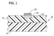
- FIG. 1is a schematic representation of a segment of an integrated circuit device shown in cross-section.
- a multilayer metal capis deposited over an interconnect feature in an electronic device substrate.
- the substrateis selected from among any substrate which has metal interconnect features, typically Cu, but in some instances Ag, in a dielectric, such as SiO 2 and low k dielectrics.
- the caphas multiple layers which serve distinct primary purposes, or has multiple distinct layers which function to achieve the same primary purposes.
- the two or more layers of the caphave different chemistries, and/or are deposited by distinct methods, under distinct conditions, to distinct thicknesses, which renders two or more layers distinct in form.
- the properties of the capcan be tailored to a particular application; e.g., to be more impervious to electromigration of interconnect metal out of the interconnect, more resistant to corrosion, and/or more resistant to etching during etch-back of subsequently deposited layers of the device. It has been discovered that because the respective two or more layers are distinct from each other in terms of chemistry, microstructure, morphology, and/or other attribute, their combined properties are enhanced in comparison to a single continuous layer of the same overall thickness.
- the metalwhich encompasses metal alloys in the context of this invention—is selected for the cap from among effective diffusion and electromigration barrier metals. Such metals are characterized by low diffusivity and low mobility under the manufacturing and service conditions encountered by the device.
- the cap metalsare specifically selected to avoid diffusion into the interconnect, because the goal is to form a distinct cap substantially entirely on top of the interconnect rather than an intermittent reaction layer of intermetallics from the interconnect and cap metals.
- Specific metals for the first, bottom-most layer of the cap adjacent the interconnectare therefore selected such that they are substantially immiscible with the Cu interconnect.
- the metalis selected from among metals in which Cu has a solubility of less than about 10 4 ⁇ exp(( ⁇ 0.75 eV/kT)at. % for a temperature between 900 and 1100° C., and less than about 10 3 ⁇ exp(( ⁇ 0.52 eV/kT)at % in the temperature region between 550 and 700° C.
- the solubility of Cu in bulk Cois ⁇ 4.5 ⁇ 10 3 ⁇ exp(( ⁇ 0.75 eV/kT)at. % for a temperature between 900 and 1100° C., ⁇ 6 ⁇ 10 2 ⁇ exp(( ⁇ 0.52 eV/kT)at % in the temperature region between 550 and 700° C.
- metals avoided in the first layer of the capare Ni, Au, and Ag due to their miscibility with Cu.
- the cap metals in all layersare selected to avoid diffusion into the adjacent Si or other substrate material. Suitable diffusivity can be determined by different criteria for different applications within the scope of the invention. Among metals avoided in the second and subsequent layers of the cap are Au and Ag due to their diffusivity and mobility in Si.
- Niis avoided as a first layer on top of Cu interconnects due to its aforementioned miscibility with Cu and because Ni tends to alter electrical conductivity characteristics of Cu by formation of Ni—Cu intermetallics.
- Cobalt-based alloysin contrast, do not significantly alter electrical conductivity characteristics of Cu.
- One of the several preferred combinations meeting these criteria and described in more detail belowinvolves a Co-based first layer because Co provides good barrier and electromigration protection for Cu.
- the cap materialsare selected such that they are electrically conducting, rather than insulating. They are also selected so they can be deposited by non-blanket deposition methods, that is, methods which are chemically selective for Cu interconnects, or for previously deposited layers of the multilayer cap.
- the inventionis a cap having two or more continuous layers wherein at least one layer is deposited by electroless plating, and the remaining layer or layers are deposited by either electroless plating or an immersion process.
- one of the layers of the capis a discontinuous layer formed by an electroless process, and the remaining layer or layers are continuous and deposited by either electroless plating or an immersion process.
- the multilayer metal capis not subsequently removed during processing, nor is it annealed to diffuse into the interconnect, and in this regard it is a permanent component distinct from the metal-filled interconnect feature.
- a component 10 of an eventual multilayer integrated circuit devicewhich includes an insulative material 12 constituting an inter-layer dielectric (ILD) on a semiconductor substrate 14 .
- a typical dielectric materialis BD (available from Applied Materials), or low k dielectrics available from Novellus Systems, Inc. of San Jose, Calif. under the trade name Coral.
- a typical semiconductor substrateis monocrystalline Si.
- An interconnect feature at the top surface of the featureis filled with Cu metallization 16 .
- the multilayer cap of the inventioncomprises first metal cap layer 18 and second metal cap layer 20 .
- There is a barrier layer such as TaN in the interconnect between the Cu metallization and the insulative material 12but this barrier layer is not shown in FIG. 1 to preserve clarity of the schematic.
- the multilayer caphas a first layer which comprises, e.g., Co—B, Co—B—P, Co—W—B—P, or Co—B—W deposited by borane-chemistry electroless deposition process employing an alkylamine borane compound such as dimethylaminoborane (DMAB), diethylaminoborane (DEAB), or morpholine borane as a reducing agent.
- DMABdimethylaminoborane
- DEABdiethylaminoborane
- morpholine boranea reducing agent.
- the processis therefore self-initiating on Cu interconnects, so Co, Pd, or other seeding operation is omitted.
- Thisis in contrast to electroless processes based on non-borane chemistry, such as employing hypophosphite or other non-borane reducing agents, which do not render Cu catalytic to Co deposition.
- the non-borane processesif used to build a layer directly on a Cu interconnect, require Co seeding or other initiation mechanism.
- this borane-chemistry electroless depositionis performed only to the extent a Co-based layer on the order of about 5 to about 50 angstroms (e.g, about 5 to about 20 angstroms) is formed.
- this first layeris substantially entirely coalesced to provide coverage which is substantially continuous.
- the first layeris significantly uncoalesced such that its coverage is significantly discontinuous.
- a second Co-based layer thicker than about 100 angstromsis then deposited by an alternative deposition process, such as by electroless deposition employing a hypophosphite reducing agent, or a mixture of reducing agents.
- a non-borane processsuch as an electroless process using a hypophosphite reducing agent is suitable because hypophosphite renders the Co-based first layer catalytic to deposition of a Co-based second layer.
- the multilayer caphas a Co-based first layer which is on the order of about 100 angstroms thick or thicker, such as in the range of about 100 to about 300 angstroms, and comprises a composition such as Co—B, Co—B—P, Co—W—B—P, or Co—B—W deposited employing an alkylamine borane such as DMAB, DEAB, or morpholine borane as a reducing agent.
- a second Co-based layeralso of similar thickness greater than 100 angstroms is then deposited by an alternative deposition process, such as by electroless Co deposition employing a hypophosphite reducing agent or mixture of reducing agents.
- the multilayer caphas a first layer which is on the order of about 100 angstroms thick or thicker, such as in the range of about 100 to about 300 angstroms, and comprises a composition such as Co—B, Co—B—P, Co—W—B—P, or Co—B—W deposited by self-initiated electroless deposition employing an alkylamine borane such as DMAB, DEAB, or morhpholine borane as a reducing agent.
- a second Ni-based layere.g., Ni—Co
- other non-Co-based layeralso of greater than 100 angstroms is then deposited by an alternative deposition process, such as by conventional electroless deposition.
- the multilayer caphas a first layer which is a Co seed layer.
- a seed layerAs a seed layer, it is significantly discontinuous and uncoalesced. In the areas where there is coverage, it is especially thin (e.g., 10 angstroms or less).
- This seed layermay be applied by conventional seeding techniques such as PVD or CVD of a catalytic metal or Co or Ni, or by self-initiated borane-chemistry electroless deposition employing an alkylamine borane reducing agent such as DMAB, DEAB, or morpholine borane as reducing agent.
- a second layeris on the order of about 100 angstroms thick or thicker, such as in the range of about 100 to about 300 angstroms, and comprises Co-based compositions such as Co—W—P or Co—W—B, and is deposited by electroless deposition.
- a third layeris a Co-based, Ni-based, or other non-Co-based layer also greater than about 100 angstroms deposited by the same or an alternative deposition process.
- each layeris therefore compositionally modulated by adjustment of one or more deposition parameters.
- each of two adjacent layersmay be deposited using the same bath and identical conditions except that the pH and/or temperature during deposition of the second adjacent layer is different from the pH and/or temperature during deposition of the first layer.
- Other conditions which can be modulated to affect compositioninclude tool-related effects, such as bath agitation, substrate rotation and rotation speed, solution flow rate, and the like.
- the pH, temperature, and all the other parametersare the same for each layer, but the compositions are distinct in that the first layer comprises Co—B and a second layer comprises Co—B—W.
- Multi of the multilayer caprefers to two, three, or more layers. From a strictly cost and process engineering perspective, it is most typical to employ just two layers, because less operations are involved. However, there may be situations where three, four, or more layers are preferred. For example, three or four layers may be preferred in certain instances when the cap serves several functions. Other alternatives are to replace one of the relatively thicker (100+ angstrom) layers with a layer of moderate thickness, such as between about 60 and about 100 angstroms.
- cap of the inventionserves as a barrier to electromigration of Cu.
- Ternary Co-based alloyshave been discovered to be especially advantageous for this purpose.
- at least one of the layersemploys one of the following alloys:
- the components of the ternary and more complex alloys for use with the inventioninclude a barrier element, Co, which is selected in significant part because it is immiscible with Cu, and therefore does not tend to alloy with Cu during assembly or over time during service.
- a second componentis the refractory element such as W, Mo, or Re which functions to increase thermal stability, corrosion resistance, and diffusion resistance.
- a third componentis P or B present as a consequence of decomposition of the reducing agent. An effect of these elements is to reduce grain size, which can render the microstructure more impervious to Cu electromigration.
- COWB with high W contenthas a phase which appears to approach overall amorphousness. Without being bound to a particular theory, it is believed that the presence of refractory metal together with B and P improves the barrier properties by filling in the grain boundaries of the crystalline structure of the capping film.
- One or more of the layers of the capmay comprise a quaternary alloy.
- Another function performed by the cap in many of the applications of the invention, as noted above,is to provide an etch stop layer to inhibit damage to interconnects during subsequent etching operations.
- Another function which may be performed by the capis resistance to chemical erosion.
- process stepsare carried out including preparation of the substrate, self-initiated electroless deposition, surface activation, complexation rinsing, and electroless deposition, as described in more detail below.
- one or more acidsis employed for mildly etching interlayer dielectric (ILD), and one or more acids is employed for dissolving Cu oxide.
- ILDinterlayer dielectric
- alkaline solutionsmay be preferred for etching certain substrates.
- a first pretreatment operationinvolves exposing the substrate to an acid selected from among HF, NH 4 F, H 2 SO 4 for mildly etching the dielectric to remove Cu embedded in the dielectric by CMP.
- an acidselected from among HF, NH 4 F, H 2 SO 4 for mildly etching the dielectric to remove Cu embedded in the dielectric by CMP.
- HF acid etchfor this purpose is a 500:1 buffered hydroflouric (BHF) acid etch.
- the substrateis rinsed by, e.g., DI water.
- a second pretreatmentemploys an organic or inorganic acid or basic cleaner for removing oxide from the metal interconnect feature.
- This cleanerpreferably removes all the oxide, for example copper oxide, without removing substantial amounts of the metallization in the interconnects. Unless removed, the oxide can interfere with adhesion of the cap and can detract from electrical conductivity.
- Cleaners of this typeare known and typically contain an etching agent such as a weak solution of an acid with less than 10 wt % in water of a strong mineral acid such as HF, HNO 3 , or H 2 SO 4 or a weak organic or carboxylic acid such as citric or malonic acid.
- Such cleanersalso include a surfactant to help wet the surface, such as Rhodafac RE620 (Rhone-Poulenc).
- An alternative acid cleanercontains citric acid and boric acid at pH 6.5.
- Typical basic cleanerscontain TMAH with addition of hydroxlyamine, MEA, TEA, EDA (ethylenediamine), or DTA (diethylenetriamine) at pH range of 9 to 12.
- certain embodiments of the inventioninvolve deposition of a first Co-based layer by electroless deposition employing borane chemistry.
- This exposuremay comprise dip, flood immersion, spray, or other manner of exposing the substrate to a deposition bath, with the provision that the manner of exposure adequately achieve the objectives of depositing a Co-based cap of the desired thickness and integrity.
- the inventionemploys a borane-based reducing agent such as an alkylamine borane reducing agent, for example DMAB, DEAB, morpholine borane, mixtures thereof, or mixtures thereof with hypophosphite.
- a borane-based reducing agentsuch as an alkylamine borane reducing agent, for example DMAB, DEAB, morpholine borane, mixtures thereof, or mixtures thereof with hypophosphite.
- Oxidation/reduction reactions involving the borane-based reducing agents and Co ionsare catalyzed by Cu.
- the reducing agentsare oxidized in the presence of Cu, thereby reducing ionic Co to Co metal which deposits on the Cu.
- One currently preferred reducing agent systememploys about 1 g/L DMAB reducing agent in a mixture with about 10 g/L hypophosphite reducing agent.
- the processis substantially self-aligning in that the Co is deposited essentially only on the Cu interconnect, such that the process is maskless because there is no need to mask areas other than the interconnect. Moreover, there is no need to subsequently remove substantial amounts of stray Co deposition from the dielectric.
- the self-initiating electroless Co deposition bathcomprises a source of Co ions which are introduced into the solution as an inorganic Co salt such as chloride and/or sulfate or other suitable inorganic salts, or an inorganic complex such as pyrophosphate, or a Co complex with an organic carboxylic acid such as Co acetate, citrate, lactate, succinate, propionate, hydroxyacetate, EDTA or others in the range of between about 1 and about 20 g/L Co 2+ .
- an inorganic Co saltsuch as chloride and/or sulfate or other suitable inorganic salts
- an inorganic complexsuch as pyrophosphate
- a Co complex with an organic carboxylic acidsuch as Co acetate, citrate, lactate, succinate, propionate, hydroxyacetate, EDTA or others in the range of between about 1 and about 20 g/L Co 2+ .
- the bathmay also contain an alkali-free source of refractory metal ions.
- the level of refractory metal ions in the deposition bathis between 0 and up to on the order of about 50 g/L of refractory metal salt in the solution.
- the refractory metalis selected from among W, Re, Mo, and mixtures thereof.
- the bathfurther contains one or more complexing agents and buffering agents.
- the complexing agents used in the bathare selected from among citric acid, malic acid, glycine, propionic, succinic, lactic acids, DEA, TEA, and ammonium salts such as ammonium chloride, ammonium sulphate, ammonium hydroxide, pyrophosphate, and mixtures thereof.
- the buffering agentsare selected from among ammonium, borate, phosphate, acetate, and mixtures thereof.
- ammonium, TMAH, or mixtures thereofare typical for alkaline pH adjustment.
- Sulfuric, hydrochloric, and citric acidsare used for acidic pH adjustment, with the acid selection made to correlate to the anion of the Co source.
- one electroless bath for self-initiated depositioncontains the following constituents, by weight:
- certain embodiments of the inventionemploy an electroless Co-based deposition process which does not employ a reducing agent which renders Cu catalytic to Co deposition.
- a surface activation operationis employed to facilitate subsequent electroless deposition.
- a currently preferred surface activation processutilizes a Pd immersion reaction.
- Other known hydrogenation/dehydrogenation catalysts for organic synthesisare suitable and include Rh, Ru, Pt, Ir, and Os.
- the surfacemay be prepared for electroless deposition by seeding as with, for example, Co seeding deposited by PVD, CVD, or other technique as is known in the art.
- Palladium chloride(PdCl 2 ) is a readily available Pd source for the preferred surface activation process.
- the trend with the present inventionis to bias the pH toward milder conditions, such as by buffering the pH to 2 and higher by use of a phosphate or other known buffering agent. It has been discovered that by buffering the pH, excess etching of the Cu interconnects on the substrate is minimized.
- a preferred source of borateis boric acid which is neutralized to tetramethyl ammonium borate in the working solution.
- a ligandis required to keep the Pd ions in solution. While maintaining Pd in solution, one challenge is not to form too highly complexed of a Pd complex, because the ultimate goal is to have the Pd release and deposit onto the Cu in reasonable deposition times, such as about 30 seconds or less.
- Bromideis one preferred ligand in the activation process of the invention. Bromide may be provided by HBr. It has been discovered that bromide between about 50 ppm and about several grams/L allows use of lower PdCl 2 (e.g., 10 ppm) concentration because bromide-Pd complexes are not too strong and not too weak.
- Bromide-Pd complexesare therefore not so strong that they do not readily release for deposition onto the substrate, yet they are not so weak that they release too readily such that selectivity is lost. With bromide-Pd complexes, therefore, selectivity is enhanced, which provides an added benefit that the amount of Pd in the solution can be lower than if other complexes are employed.
- Such bromide levelsachieve acceptable Pd deposition initiation rates of less than about 30 seconds. In particular, at 10 ppm Pd, 120 ppm bromide, and a pH of 4, acceptable initiation rates are achieved with no appreciable Cu etch.
- Sources of Pd 2+ other than PdCl 2include PdSO 41 PdBr 2 , Pd(NO 3 ) 2 , palladium acetate, and palladium propionate.
- the complexing ligand for stabilizing the Pd 2+is citrate, acetic acid, or MSA.
- An acid or mixture of acids correlating to the anion of the Pd compoundsuch as the exemplary inorganic acids hydrochloric, hydrobromic, sulfuric, and phosphoric is used for pH adjustment. Less aggressive acids are preferred in many instances to alleviate problems of microtrenching at the interface between Cu and Ta or other barrier on the dielectric.
- Such acidsare optionally organic acids such as organic aliphatic mono- & di-carboxylic acids (glycolic, succinic, oxalic, lactic, trifluoroacetic (halogen-substituted)), aromatic mono- & di-carboxylic acids (benzoic, phtalic), aromatic sulfonic or sulfinic (benzenesulfonic, toluenesulfonic, cumenesulfonic, xylenesulfonic, phenolsulfonic, cresolsulfonic, naphtalenesulfonic, and analogous-sulfinics), aromatic phosphonic or phosphinic, or inorganic Acids with reducing properties (hypophosphorous, sulfurous).
- Palladium sourcesare typically, but not necessarily, selected to have an anion correlating to such acids not necessarily.
- a second challenge in formulating activation chemistryis selectivity of deposition for the metal over the dielectric, to avoid forming activation sites on the dielectric surface. This challenge is addressed by combination of pre-cleaning, Pd activation chemistry, and post activation cleaning/complexing rinse as described herein.
- the processis substantially self-aligning in that the activator is deposited essentially only on the Cu interconnect, such that the process is maskless because there is no need to mask areas other than the interconnect.
- a surfactant such as Calsoft LAS99can optionally be used to improve wetting.
- the substrateAfter activation, the substrate is exposed to a complexing rinse, which functions to remove residual ionic activator left behind by the activator composition, and thereby minimize subsequent deposition on unintended surfaces.
- the inventionin several aspects also involves electroless deposition which employs reducing agents other than the borane-based reducing agents described above.
- depositionis one of the options used when forming a) a first layer, provided the Cu substrate is either activated or seeded as described above, b) a second layer on top of a Co-based first layer, or c) a third or subsequent layer on top of a second or subsequent layer.
- the inventionemploys an electroless metal deposition layer deposited with the assistance of a reducing agent which i) renders a metal seed on the Cu catalytic to deposition, or ii) assists with Pd-catalyzed deposition of an activated Cu substrate.
- the inventionemploys an electroless Co and/or Ni and/or other metal deposition layer deposited with the assistance of a reducing agent which renders the previously applied Co-based layer catalytic to deposition of the next layer.
- an electroless bathcomprising a source of Co ions and a reducer.
- the Co ionsare introduced into the solution as an inorganic Co salt such as chloride and/or sulfate or a Co complex with an organic carboxylic acid such as Co acetate, citrate, lactate, succinate, propionate, or hydroxyacetate in the range of between about 2 and about 50 g/L Co.
- One or more reducing agentssuch as a hypophosphite reducing agent (e.g., ammonium hypophosphite) is employed in a concentration roughly between about 2 and about 30 g/L.
- the reducing agentis alkali-free; and particularly Na-free.
- Other reducing agentsare described in Mallory and Hajdu (Eds.), Electroless Plating, Fundamentals and Applications , American Electroplaters and Surface Finishers Society (1990), as well as numerous electroless bath compositions and reaction chemistries for Ni and Co electroless plating.
- a hypophosphite or other reducing agentis supplemented with a borane-based reducing agent.
- the bathfurther may also contain an alkali-free source of refractory metal ions.
- the level of refractory metal ions in the deposition bathin a concentration between 0 and up to on the order of about 50 g/L refractory metal salt.
- the refractory metalis selected from among W, Re, Mo, and mixtures thereof.
- W ionsare provided by an alkali-free, tungstate-based source of W ions.
- sources of W ionsare tetramethylammonium tungstate, phosphotungstate, silicotungstate, and mixtures thereof.
- one preferred deposition bathcontains between about 2 and about 10 g/L tungstic acid neutralized by TMAH.
- sources of refractory metalinclude ammonium molybdate.
- a stabilizer for the Cois incorporated into one preferred embodiment of the electroless Co deposition bath.
- the Co complexesare stable in solution in the absence of a reducing agent, the use of a stabilizer can help prevent spontaneous decomposition of the bath components.
- Exemplary stabilizersinclude, for example, Pb, Bi, Sn, Sb, IO 3 , MoO 3 , AsO 3 azoles such as imidazole and derivatives.
- the stabilizer levelis on the order of between about 0.1 and about 100 ppm. For example, for Pb+ 2 from about 5 to about 20 ppm has been shown to be effective. For MoO 4 -2, about 10 to about 100 ppm has been shown to be effective.
- maleic acidis a stabilizer within the four classes discussed in Mallory and Hajdu (Eds.), Electroless Plating, Fundamentals and Applications , American Electroplaters and Surface Finishers Society (1990) (p. 34-44).
- a grain refiner for the deposited Cois optionally incorporated into the bath.
- This grain refinercan also be characterized as a stabilizer, but this grain refiner is distinguished from the stabilizers described above in that those stabilizers do not primarily perform a grain refining function.
- Exemplary grain refinersinclude, for example, Cd, Cu, Al, saccharine, 2-butyne-1,4,-diol and its alkoxylates, 3-hexyne-2,5,-diol, propargyl alcohol and its alkoxylates and sulfonates, alyl sulfonate, betaine and its sulfobetaine derivatives.
- the bathtypically contains a pH buffer to stabilize the pH in the desired range.
- the desired pH rangeis between about 8.0 and about 10.0. If the pH is not stabilized, unintentional, undesirable, and unanticipated changes in deposition rate and deposit chemistry can occur.
- Exemplary buffersinclude, for example, borates, tetra- and pentaborates, phosphates, acetates, glycolates, lactates, ammonia, and pyrophosphate.
- the pH buffer levelis on the order of between about 10 and about 50 g/L.
- a complexing agent for the Cois included in the bath to help keep the Co in solution.
- the bathis typically operated at a pH of between about 8 and about 10, at which level the Co can have a tendency to form hydroxides and precipitate out of solution.
- exemplary complexing agentsinclude citrate, glycolic acid, lactic acid, malic acid, succinic acid, pyophosphate, ammonium, DEA, TEA, and EDTA.
- the complexing agent concentrationis selected such that the molar ratio between the complexing agent and Co is between about 2:1 and about 4:1, generally.
- the level of complexing agentmay be on the order of between about 20 g/L and about 120 g/L.
- One or more surfactantsis optionally included in the bath to help wet the substrate surface.
- the surfactantalso can serve as a mild deposition inhibitor which can suppress three-dimensional growth to an extent, thereby improving morphology and topography of the film. It can also help refine the grain size, which yields a more uniform coating which has grain boundaries which are less porous to migration of Cu.
- Exemplary anionic surfactantsinclude alkyl phosphonates, alkyl ether phosphates, alkyl sulfates, alkyl ether sulfates, alkyl sulfonates, alkyl ether sulfonates, carboxylic acid ethers, carboxylic acid esters, alkyl aryl sulfonates, and sulfosuccinates.
- Exemplary non-ionic surfactantsinclude alkoxylated alcohols, ethoxy/propoxy (EO/PO) block copolymers, alkoxylated fatty acids, glycol and glycerol esters, with polyethylene glycols, and polypropylene glycol/polyethylene glycol currently preferred.
- the level of surfactantis on the order of between about 0.01 and about 5 g/L.
- one electroless bath for deposition as disclosed in Shacham-Diamand, Journal of Electrochemical Society “Electroless Deposition of Thin-Film Co—W—P Layers” (2001)contains the following constituents: 23 g/L CoSO 4 —H 2 O 21 g/L NaH 2 PO 2 130 g/L Na citrate 10 g/L Na 2 WO 4 —H 2 O 0.05 g/L Rhodafac RE-610 Balance water pH about 9.0
- Another suitable bath disclosed thereincontains the following: 23 g/L CoSO 4 —H 2 O 21 g/L NaH 2 PO 2 130 g/L Na citrate 10 g/L H 3 P(W 3 O 10 ) 4 0.05 g/L Rhodafac RE-610 Balance water pH about 9.0
- a further suitable bathis disclosed in Pat. No. 5,695,810: 10 g/L (NH 4 ) 2 WO 4 30 g/L CoCl 2 —6H 2 O 80 g/L Na 3 C 6 H 4 O 7 —2H 2 O 20 g/L Na 2 H 2 PO 2 0.05 g/L Rhodafac RE610
- This electroless processlike the above-described process employing a borane-based reducing agent, is substantially self-aligning in that the electroless metal is deposited essentially only onto the metal interconnect, or onto a previously deposited metal cap layer in the situation of a second or subsequent layer in multilayer deposition.
- the processtherefore does not require lithography and its several steps of patterning, stripping etc. Moreover, there is no need to subsequently remove substantial amounts of unintended cap metal deposition from the dielectric.
- one or more of the layers of the multilayer capmay alternatively be applied by a metal immersion process as is known in the art.
- immersion platingalso known as displacement plating
- a metal on a surfaceis displaced by a metal ion in an immersion reaction.
- the driving forceis a lower oxidation potential of the metal ion in the solution.
- Immersion plating parametersare disclosed in Hirsch et al., “Immersion Plating,” Metal Finishing Guidebook, 1989, pp. 402-406.
- the base metal on the surfacefunctions as the reducing agent. Immersion plating therefore differs from electroless plating in that a further reducing agent is not required.
- the substrateis a dielectric material in which one or more, typically many, interconnect features have been formed.
- the capis built up on top of the interconnect feature and, dimensionally, forms an extension comprising layers 18 and 20 ( FIG. 1 ) on the top of the interconnect feature. Accordingly, the interconnect/cap combination is dimensionally larger than the interconnect prior to capping.
- the exposed surface of an interconnect feature prior to cappingis typically roughly co-planar with a flat top surface of the dielectric material.
- This co-planarityis achieved by CMP to remove metal—metal typically applied over the entire dielectric and into interconnect features by a previous electrodeposition operation—from the top surface of the dielectric.
- the only metal left on the substrate after the CMP operationis the exposed metal in the interconnect features, plus perhaps some trace metal embedded into the dielectric by the CMP, though this trace metal is typically removed by an above-described cleaning operation.
- the multilayer cap applied by this inventionextends above the plane defined by the flat top surface of the dielectric material with which the exposed surface of the interconnect feature is co-planar. Depositing the cap in these instances therefore involves building cap material on top of the metal interconnect such that the cap extends above the plane of the dielectric.
- the multilayer capwhich dimensionally constitutes an extension on top of the wiring, is permanent in that it is not removed in subsequent processing.
- an etch stop layeris typically applied over the entire top surface of the dielectric and any cap extensions covering interconnects. In the present invention, this is performed without any intermittent chemical, mechanical, or other operation to remove the cap extensions. Most typically, the etch stop layer is applied directly over the top surface of the dielectric and directly over any cap extensions covering interconnects. This is also accomplished without an intermittent annealing operation because the Co-based cap serves its protective capping function without such an anneal.
- the eventual multilayer integrated circuit devicemay be incorporated into an electronic package by way of an external electrical connector, such as a wire bond structure.
- the devicecomprises a series of dielectric layers between which are metal interconnects with caps thereon.
- the multilayer cap of the inventionis a barrier on top of Cu interconnects embedded in dielectric.
Landscapes
- Engineering & Computer Science (AREA)
- Microelectronics & Electronic Packaging (AREA)
- Manufacturing & Machinery (AREA)
- Computer Hardware Design (AREA)
- Power Engineering (AREA)
- Physics & Mathematics (AREA)
- Condensed Matter Physics & Semiconductors (AREA)
- General Physics & Mathematics (AREA)
- Internal Circuitry In Semiconductor Integrated Circuit Devices (AREA)
- Chemically Coating (AREA)
- Electrodes Of Semiconductors (AREA)
Abstract
Description
- This invention relates to integrated circuit manufacture and, in particular, to metal-based capping of interconnect metallization.
- In damascene processing metallization is employed to form electrical interconnects in an integrated circuit substrate by metal-filling of interconnect features such as vias and trenches formed in the substrate. If the metal deposited on such a substrate is Cu, it can diffuse rapidly into the Si substrate and dielectric films as, for example, SiO2or low k dielectrics. Copper can also diffuse into a device layer built on top of a substrate in multilayer device applications. Such diffusion can be detrimental to the device because it can cause electrical leakage in substrates, or form an unintended electrical connection between two interconnects resulting in an electrical short. And the corresponding diffusion out of the interconnect feature can disrupt electrical flow therethrough.
- Metal deposited on the substrate also has a tendency to migrate out of the interconnect feature when electrical current passes through the feature in service. Electron bombardment of the metal moves the metal out of the feature. This migration can damage an adjacent interconnect line, cause junction leakage, form unintended electrical connections, and disrupt electrical flow in the feature from which the metal migrates.
- Accordingly, among the challenges facing integrated circuit device manufacturers is to minimize diffusion and electromigration of metal out of metal-filled interconnect features. This challenge becomes more acute as the devices further miniaturize, and as the features further miniaturize and densify.
- Another challenge in the context of metal interconnect features is to protect them from corrosion. Certain interconnect metals, especially Cu, are more susceptible to corrosion.
- Copper is a fairly reactive metal which readily oxidizes under ambient conditions. This reactivity can undermine adhesion to dielectrics and thin films, resulting in voids and delamination. Another challenge is therefore to combat oxidation and enhance adhesion between the cap and the Cu, and between structure layers.
- To address these challenges the industry has employed a variety of diffusion barrier films as a cap over Cu and other metal interconnect features. Refractory metals and their alloys have been deposited in thin films by physical vapor deposition (PVD). SiN and SiC have been deposited for this purpose by chemical vapor deposition (CVD). A limitation of SiN and SiC is that they have a relatively high dielectric constant (k value), which tends to increase capacitance of the interconnect. An increase in capacitance can increase power dissipation due to resistance/capacitance coupling (RC delay), thereby limiting the performance.
- In general, barrier or capping layer formation by blanket vapor deposition is expensive and time-consuming, as it involves multiple processing steps. The deposited films need to be patterned and etched, followed by resist removal. Some degree of misalignment is expected with lithographic patterning.
- Electroless Co and Ni have been discussed as a protective layer over electrical interconnect lines in, for example, U.S. patent publication No. 2003/0207560.
- Chemical mechanical polishing (CMP) is performed on a substrate prior to capping and following via formation to, for example, remove unwanted Cu overburden deposited during damascene processing and thereby planarize the surface. This CMP can cause traces of copper to be embedded or smeared onto the dielectric material. These traces of copper, if not removed, can contaminate the dielectric. The traces of Cu can have a detrimental effect on the selectivity of a Co-capping process by causing deposition of electroless Co on the dielectric between the Cu traces, which can result in junction leakage. An etchant is therefore employed in a pretreatment composition to either remove these traces of copper, undercut the dielectric on which they reside, or both.
- According to conventional wet processing, sequences separate cleaning solutions are employed for cleaning of dielectric, and for cleaning of the metal. Dielectric cleaner lightly etches the dielectric surface in order to undercut metal traces embedded onto the dielectric during CMP. Metal cleaner removes surface oxides on Cu and any remaining traces of Cu embedded in the dielectric that were not removed during the dielectric cleaning step. A cleaner may be necessary to remove residues from Cu inhibitors such as benzotriazole (BTA) compounds used during CMP processing so that such residues do not interfere with effectiveness of activation, uniformity of activation and initiation, smoothness of cap deposition, adhesion of capping deposit, and thermal stability of the cap.
- Briefly, therefore, the invention is directed a method for forming a multilayer metal cap over a metal-filled interconnect feature in an integrated circuit substrate for incorporation into a multilayer integrated circuit device comprising. The method involves depositing a first metal cap layer over the metal-filled interconnect feature in a first deposition process which constitutes electroless metal deposition from an electroless bath comprising a source of metal ions and a reducing agent; and depositing a second metal cap layer over the first metal cap layer in a second deposition process distinct from the first deposition process to thereby form the multilayer metal cap as a permanent component distinct from the metal-filled interconnect feature.
- The invention is also directed to a multilayer cap over a metal-filled interconnect feature in an integrated circuit substrate formed by the foregoing method, and to an integrated circuit substrate comprising a multilayer cap over a metal-filled interconnect feature formed by the foregoing method.
FIG. 1 is a schematic representation of a segment of an integrated circuit device shown in cross-section.- In accordance with this invention, a multilayer metal cap is deposited over an interconnect feature in an electronic device substrate. The substrate is selected from among any substrate which has metal interconnect features, typically Cu, but in some instances Ag, in a dielectric, such as SiO2and low k dielectrics.
- In certain preferred embodiments of the invention, the cap has multiple layers which serve distinct primary purposes, or has multiple distinct layers which function to achieve the same primary purposes. As explained further below, the two or more layers of the cap have different chemistries, and/or are deposited by distinct methods, under distinct conditions, to distinct thicknesses, which renders two or more layers distinct in form.
- Depending on various assembly and service conditions, by having such two or more distinct layers, the properties of the cap can be tailored to a particular application; e.g., to be more impervious to electromigration of interconnect metal out of the interconnect, more resistant to corrosion, and/or more resistant to etching during etch-back of subsequently deposited layers of the device. It has been discovered that because the respective two or more layers are distinct from each other in terms of chemistry, microstructure, morphology, and/or other attribute, their combined properties are enhanced in comparison to a single continuous layer of the same overall thickness.
- The purpose of the cap is to provide a distinct layer of protection over the interconnect. Accordingly, the metal—which encompasses metal alloys in the context of this invention—is selected for the cap from among effective diffusion and electromigration barrier metals. Such metals are characterized by low diffusivity and low mobility under the manufacturing and service conditions encountered by the device. The cap metals are specifically selected to avoid diffusion into the interconnect, because the goal is to form a distinct cap substantially entirely on top of the interconnect rather than an intermittent reaction layer of intermetallics from the interconnect and cap metals. Specific metals for the first, bottom-most layer of the cap adjacent the interconnect are therefore selected such that they are substantially immiscible with the Cu interconnect. Substantially immiscible means that some insignificant amount of miscibility is tolerated, but the metals are at least sufficiently immiscible that there is no significant reduction in performance due to miscibility under expected service conditions. While suitable immiscibility can be determined by different criteria for different applications within the scope of the invention, in one aspect, the metal is selected from among metals in which Cu has a solubility of less than about 104×exp((−0.75 eV/kT)at. % for a temperature between 900 and 1100° C., and less than about 103×exp((−0.52 eV/kT)at % in the temperature region between 550 and 700° C. The solubility of Cu in bulk Co is ˜4.5×10³×exp((−0.75 eV/kT)at. % for a temperature between 900 and 1100° C., ˜6×10²×exp((−0.52 eV/kT)at % in the temperature region between 550 and 700° C. Among metals avoided in the first layer of the cap are Ni, Au, and Ag due to their miscibility with Cu.
- The cap metals in all layers are selected to avoid diffusion into the adjacent Si or other substrate material. Suitable diffusivity can be determined by different criteria for different applications within the scope of the invention. Among metals avoided in the second and subsequent layers of the cap are Au and Ag due to their diffusivity and mobility in Si.
- As a general proposition, Ni is avoided as a first layer on top of Cu interconnects due to its aforementioned miscibility with Cu and because Ni tends to alter electrical conductivity characteristics of Cu by formation of Ni—Cu intermetallics. Cobalt-based alloys, in contrast, do not significantly alter electrical conductivity characteristics of Cu. One of the several preferred combinations meeting these criteria and described in more detail below involves a Co-based first layer because Co provides good barrier and electromigration protection for Cu.
- The cap materials are selected such that they are electrically conducting, rather than insulating. They are also selected so they can be deposited by non-blanket deposition methods, that is, methods which are chemically selective for Cu interconnects, or for previously deposited layers of the multilayer cap.
- Within the foregoing material selection criteria, in one aspect the invention is a cap having two or more continuous layers wherein at least one layer is deposited by electroless plating, and the remaining layer or layers are deposited by either electroless plating or an immersion process. In another aspect of the invention one of the layers of the cap is a discontinuous layer formed by an electroless process, and the remaining layer or layers are continuous and deposited by either electroless plating or an immersion process. The multilayer metal cap is not subsequently removed during processing, nor is it annealed to diffuse into the interconnect, and in this regard it is a permanent component distinct from the metal-filled interconnect feature.
- As shown schematically and not-to-scale in cross-section in
FIG. 1 , in one embodiment of the invention there is acomponent 10 of an eventual multilayer integrated circuit device which includes aninsulative material 12 constituting an inter-layer dielectric (ILD) on asemiconductor substrate 14. A typical dielectric material is BD (available from Applied Materials), or low k dielectrics available from Novellus Systems, Inc. of San Jose, Calif. under the trade name Coral. A typical semiconductor substrate is monocrystalline Si. An interconnect feature at the top surface of the feature is filled withCu metallization 16. The multilayer cap of the invention comprises firstmetal cap layer 18 and secondmetal cap layer 20. There is a barrier layer such as TaN in the interconnect between the Cu metallization and theinsulative material 12, but this barrier layer is not shown inFIG. 1 to preserve clarity of the schematic. - The invention is further understood by examination of at least five more specific, nonexclusive examples from among the numerous embodiments within the scope of the invention. In a first example of the invention the multilayer cap has a first layer which comprises, e.g., Co—B, Co—B—P, Co—W—B—P, or Co—B—W deposited by borane-chemistry electroless deposition process employing an alkylamine borane compound such as dimethylaminoborane (DMAB), diethylaminoborane (DEAB), or morpholine borane as a reducing agent. These borane-based reducing agents render Cu catalytic to Co deposition. The process is therefore self-initiating on Cu interconnects, so Co, Pd, or other seeding operation is omitted. This is in contrast to electroless processes based on non-borane chemistry, such as employing hypophosphite or other non-borane reducing agents, which do not render Cu catalytic to Co deposition. The non-borane processes, if used to build a layer directly on a Cu interconnect, require Co seeding or other initiation mechanism. In this first embodiment of the invention, this borane-chemistry electroless deposition is performed only to the extent a Co-based layer on the order of about 5 to about 50 angstroms (e.g, about 5 to about 20 angstroms) is formed. In one version of this embodiment this first layer is substantially entirely coalesced to provide coverage which is substantially continuous. In a different version of this embodiment, the first layer is significantly uncoalesced such that its coverage is significantly discontinuous. A second Co-based layer thicker than about 100 angstroms is then deposited by an alternative deposition process, such as by electroless deposition employing a hypophosphite reducing agent, or a mixture of reducing agents. A non-borane process such as an electroless process using a hypophosphite reducing agent is suitable because hypophosphite renders the Co-based first layer catalytic to deposition of a Co-based second layer.
- In a second example of the invention, the multilayer cap has a Co-based first layer which is on the order of about 100 angstroms thick or thicker, such as in the range of about 100 to about 300 angstroms, and comprises a composition such as Co—B, Co—B—P, Co—W—B—P, or Co—B—W deposited employing an alkylamine borane such as DMAB, DEAB, or morpholine borane as a reducing agent. A second Co-based layer also of similar thickness greater than 100 angstroms is then deposited by an alternative deposition process, such as by electroless Co deposition employing a hypophosphite reducing agent or mixture of reducing agents.
- In a third example of the invention, the multilayer cap has a first layer which is on the order of about 100 angstroms thick or thicker, such as in the range of about 100 to about 300 angstroms, and comprises a composition such as Co—B, Co—B—P, Co—W—B—P, or Co—B—W deposited by self-initiated electroless deposition employing an alkylamine borane such as DMAB, DEAB, or morhpholine borane as a reducing agent. A second Ni-based layer (e.g., Ni—Co) or other non-Co-based layer also of greater than 100 angstroms is then deposited by an alternative deposition process, such as by conventional electroless deposition.
- In a fourth example of the invention, the multilayer cap has a first layer which is a Co seed layer. As a seed layer, it is significantly discontinuous and uncoalesced. In the areas where there is coverage, it is especially thin (e.g., 10 angstroms or less). This seed layer may be applied by conventional seeding techniques such as PVD or CVD of a catalytic metal or Co or Ni, or by self-initiated borane-chemistry electroless deposition employing an alkylamine borane reducing agent such as DMAB, DEAB, or morpholine borane as reducing agent. A second layer is on the order of about 100 angstroms thick or thicker, such as in the range of about 100 to about 300 angstroms, and comprises Co-based compositions such as Co—W—P or Co—W—B, and is deposited by electroless deposition. A third layer is a Co-based, Ni-based, or other non-Co-based layer also greater than about 100 angstroms deposited by the same or an alternative deposition process.
- In a fifth example of the invention there are two or more adjacent layers deposited using a) the same electroless plating bath under different conditions, or b) different electroless baths under different conditions, or c) different electroless plating baths under the same conditions. Each layer is therefore compositionally modulated by adjustment of one or more deposition parameters. For example, each of two adjacent layers may be deposited using the same bath and identical conditions except that the pH and/or temperature during deposition of the second adjacent layer is different from the pH and/or temperature during deposition of the first layer. Other conditions which can be modulated to affect composition include tool-related effects, such as bath agitation, substrate rotation and rotation speed, solution flow rate, and the like. Or, the pH, temperature, and all the other parameters are the same for each layer, but the compositions are distinct in that the first layer comprises Co—B and a second layer comprises Co—B—W.
- These five more specific, nonexclusive examples from among the several embodiments within the invention can therefore be summarized as follows:
- Ex I.
- Layer 1: Co-based layer of low thickness formed by electroless deposition using an alkylamine borane reducing agent
- Layer 2: Co-based layer >100 angstroms formed by electroless deposition process distinct from the process of layer 1
- Ex. II
- Layer 1: Co-based layer >100 angstroms formed by electroless deposition using alkylamine borane reducing agent
- Layer 2: Co-based layer >100 angstroms formed by electroless deposition process distinct from the process of layer 1
- Ex. III
- Layer 1: Co-based layer >100 angstroms formed by electroless deposition using alkylamine borane reducing agent
- Layer 2: Ni-based layer >100 angstroms
- Ex. IV
- Layer 1: Co-based seed layer
- Layer 2: Co-based layer >100 angstroms formed by electroless deposition
- Layer 3: Co- or Ni-based electroless layer >100 angstroms
- Ex. V
- Layer 1: Co-based layer >100 angstroms formed by electroless deposition
- Layer 2: Co-based layer >100 angstroms formed by electroless deposition
- Ex I.
- Alternatives within the foregoing embodiments are to employ two, three, or more distinct deposition operations such that “multi” of the multilayer cap refers to two, three, or more layers. From a strictly cost and process engineering perspective, it is most typical to employ just two layers, because less operations are involved. However, there may be situations where three, four, or more layers are preferred. For example, three or four layers may be preferred in certain instances when the cap serves several functions. Other alternatives are to replace one of the relatively thicker (100+ angstrom) layers with a layer of moderate thickness, such as between about 60 and about 100 angstroms.
- One function performed by the cap of the invention, as noted above, is to serve as a barrier to electromigration of Cu. Ternary Co-based alloys have been discovered to be especially advantageous for this purpose. For many of the preferred embodiments of the invention at least one of the layers employs one of the following alloys:
- Co—W—P
- Co—W—B
- Co—W—B—P
- Co—B—P
- Co—B
- Co—Mo—B
- Co—W—Mo—B
- Co—W—Mo—B—P
- Co—Mo—P
- The components of the ternary and more complex alloys for use with the invention include a barrier element, Co, which is selected in significant part because it is immiscible with Cu, and therefore does not tend to alloy with Cu during assembly or over time during service. A second component is the refractory element such as W, Mo, or Re which functions to increase thermal stability, corrosion resistance, and diffusion resistance. A third component is P or B present as a consequence of decomposition of the reducing agent. An effect of these elements is to reduce grain size, which can render the microstructure more impervious to Cu electromigration. COWB with high W content has a phase which appears to approach overall amorphousness. Without being bound to a particular theory, it is believed that the presence of refractory metal together with B and P improves the barrier properties by filling in the grain boundaries of the crystalline structure of the capping film.
- One or more of the layers of the cap may comprise a quaternary alloy.
- Another function performed by the cap in many of the applications of the invention, as noted above, is to provide an etch stop layer to inhibit damage to interconnects during subsequent etching operations.
- Another function which may be performed by the cap is resistance to chemical erosion.
- In performing the process of the invention to deposit the cap of the invention as described above, process steps are carried out including preparation of the substrate, self-initiated electroless deposition, surface activation, complexation rinsing, and electroless deposition, as described in more detail below.
- In preparing the substrate for capping, one or more acids is employed for mildly etching interlayer dielectric (ILD), and one or more acids is employed for dissolving Cu oxide. Alternatively, alkaline solutions may be preferred for etching certain substrates.
- A first pretreatment operation involves exposing the substrate to an acid selected from among HF, NH4F, H2SO4for mildly etching the dielectric to remove Cu embedded in the dielectric by CMP. For example, one known HF acid etch for this purpose is a 500:1 buffered hydroflouric (BHF) acid etch.
- After the first pretreatment operation is completed, the substrate is rinsed by, e.g., DI water.
- A second pretreatment employs an organic or inorganic acid or basic cleaner for removing oxide from the metal interconnect feature. This cleaner preferably removes all the oxide, for example copper oxide, without removing substantial amounts of the metallization in the interconnects. Unless removed, the oxide can interfere with adhesion of the cap and can detract from electrical conductivity. Cleaners of this type are known and typically contain an etching agent such as a weak solution of an acid with less than 10 wt % in water of a strong mineral acid such as HF, HNO3, or H2SO4or a weak organic or carboxylic acid such as citric or malonic acid. Such cleaners also include a surfactant to help wet the surface, such as Rhodafac RE620 (Rhone-Poulenc). An alternative acid cleaner contains citric acid and boric acid at pH 6.5.
- Typical basic cleaners contain TMAH with addition of hydroxlyamine, MEA, TEA, EDA (ethylenediamine), or DTA (diethylenetriamine) at pH range of 9 to 12.
- As a first layer on the metallization, as noted above, certain embodiments of the invention involve deposition of a first Co-based layer by electroless deposition employing borane chemistry. This exposure may comprise dip, flood immersion, spray, or other manner of exposing the substrate to a deposition bath, with the provision that the manner of exposure adequately achieve the objectives of depositing a Co-based cap of the desired thickness and integrity.
- For self-initiation of the electroless deposition, the invention employs a borane-based reducing agent such as an alkylamine borane reducing agent, for example DMAB, DEAB, morpholine borane, mixtures thereof, or mixtures thereof with hypophosphite. Oxidation/reduction reactions involving the borane-based reducing agents and Co ions are catalyzed by Cu. In particular, at certain plating conditions, e.g. pH & temperature, the reducing agents are oxidized in the presence of Cu, thereby reducing ionic Co to Co metal which deposits on the Cu. One currently preferred reducing agent system employs about 1 g/L DMAB reducing agent in a mixture with about 10 g/L hypophosphite reducing agent. The process is substantially self-aligning in that the Co is deposited essentially only on the Cu interconnect, such that the process is maskless because there is no need to mask areas other than the interconnect. Moreover, there is no need to subsequently remove substantial amounts of stray Co deposition from the dielectric.
- The self-initiating electroless Co deposition bath comprises a source of Co ions which are introduced into the solution as an inorganic Co salt such as chloride and/or sulfate or other suitable inorganic salts, or an inorganic complex such as pyrophosphate, or a Co complex with an organic carboxylic acid such as Co acetate, citrate, lactate, succinate, propionate, hydroxyacetate, EDTA or others in the range of between about 1 and about 20 g/L Co2+.
- The bath may also contain an alkali-free source of refractory metal ions. The level of refractory metal ions in the deposition bath is between 0 and up to on the order of about 50 g/L of refractory metal salt in the solution. In one embodiment, the refractory metal is selected from among W, Re, Mo, and mixtures thereof.
- The bath further contains one or more complexing agents and buffering agents. The complexing agents used in the bath are selected from among citric acid, malic acid, glycine, propionic, succinic, lactic acids, DEA, TEA, and ammonium salts such as ammonium chloride, ammonium sulphate, ammonium hydroxide, pyrophosphate, and mixtures thereof. The buffering agents are selected from among ammonium, borate, phosphate, acetate, and mixtures thereof. For pH adjustment, ammonium, TMAH, or mixtures thereof are typical for alkaline pH adjustment. Sulfuric, hydrochloric, and citric acids are used for acidic pH adjustment, with the acid selection made to correlate to the anion of the Co source.
- Within the above guidelines, one electroless bath for self-initiated deposition contains the following constituents, by weight:
- CoCl26H2O25 g/L
- Citric acid50 g/L
- Tungstic acid4 g/L
- DMAB1 g/L
- TMAH ca. 30 g/L of a 25% TMAH solution for pH adjustment
- Water Balance
- pH 9.5
- As an alternative first layer on the metallization, as noted above, certain embodiments of the invention employ an electroless Co-based deposition process which does not employ a reducing agent which renders Cu catalytic to Co deposition. For such processes a surface activation operation is employed to facilitate subsequent electroless deposition. A currently preferred surface activation process utilizes a Pd immersion reaction. Other known hydrogenation/dehydrogenation catalysts for organic synthesis are suitable and include Rh, Ru, Pt, Ir, and Os. Alternatively, the surface may be prepared for electroless deposition by seeding as with, for example, Co seeding deposited by PVD, CVD, or other technique as is known in the art.
- Palladium chloride (PdCl2) is a readily available Pd source for the preferred surface activation process. The trend with the present invention is to bias the pH toward milder conditions, such as by buffering the pH to 2 and higher by use of a phosphate or other known buffering agent. It has been discovered that by buffering the pH, excess etching of the Cu interconnects on the substrate is minimized. In buffering, a preferred source of borate is boric acid which is neutralized to tetramethyl ammonium borate in the working solution.
- In the surface activation solution a ligand is required to keep the Pd ions in solution. While maintaining Pd in solution, one challenge is not to form too highly complexed of a Pd complex, because the ultimate goal is to have the Pd release and deposit onto the Cu in reasonable deposition times, such as about 30 seconds or less. Bromide is one preferred ligand in the activation process of the invention. Bromide may be provided by HBr. It has been discovered that bromide between about 50 ppm and about several grams/L allows use of lower PdCl2(e.g., 10 ppm) concentration because bromide-Pd complexes are not too strong and not too weak. Bromide-Pd complexes are therefore not so strong that they do not readily release for deposition onto the substrate, yet they are not so weak that they release too readily such that selectivity is lost. With bromide-Pd complexes, therefore, selectivity is enhanced, which provides an added benefit that the amount of Pd in the solution can be lower than if other complexes are employed. Such bromide levels achieve acceptable Pd deposition initiation rates of less than about 30 seconds. In particular, at 10 ppm Pd, 120 ppm bromide, and a pH of 4, acceptable initiation rates are achieved with no appreciable Cu etch.
- Sources of Pd2+ other than PdCl2include PdSO41PdBr2, Pd(NO3)2, palladium acetate, and palladium propionate. The complexing ligand for stabilizing the Pd2+ is citrate, acetic acid, or MSA. An acid or mixture of acids correlating to the anion of the Pd compound such as the exemplary inorganic acids hydrochloric, hydrobromic, sulfuric, and phosphoric is used for pH adjustment. Less aggressive acids are preferred in many instances to alleviate problems of microtrenching at the interface between Cu and Ta or other barrier on the dielectric. Such acids are optionally organic acids such as organic aliphatic mono- & di-carboxylic acids (glycolic, succinic, oxalic, lactic, trifluoroacetic (halogen-substituted)), aromatic mono- & di-carboxylic acids (benzoic, phtalic), aromatic sulfonic or sulfinic (benzenesulfonic, toluenesulfonic, cumenesulfonic, xylenesulfonic, phenolsulfonic, cresolsulfonic, naphtalenesulfonic, and analogous-sulfinics), aromatic phosphonic or phosphinic, or inorganic Acids with reducing properties (hypophosphorous, sulfurous). Palladium sources are typically, but not necessarily, selected to have an anion correlating to such acids not necessarily.
- A second challenge in formulating activation chemistry is selectivity of deposition for the metal over the dielectric, to avoid forming activation sites on the dielectric surface. This challenge is addressed by combination of pre-cleaning, Pd activation chemistry, and post activation cleaning/complexing rinse as described herein.
- The process is substantially self-aligning in that the activator is deposited essentially only on the Cu interconnect, such that the process is maskless because there is no need to mask areas other than the interconnect.
- A surfactant such as Calsoft LAS99 can optionally be used to improve wetting.
- After activation, the substrate is exposed to a complexing rinse, which functions to remove residual ionic activator left behind by the activator composition, and thereby minimize subsequent deposition on unintended surfaces.
- The invention in several aspects also involves electroless deposition which employs reducing agents other than the borane-based reducing agents described above. In particular, such deposition is one of the options used when forming a) a first layer, provided the Cu substrate is either activated or seeded as described above, b) a second layer on top of a Co-based first layer, or c) a third or subsequent layer on top of a second or subsequent layer. In aspect (a), the invention employs an electroless metal deposition layer deposited with the assistance of a reducing agent which i) renders a metal seed on the Cu catalytic to deposition, or ii) assists with Pd-catalyzed deposition of an activated Cu substrate. In aspect (b), the invention employs an electroless Co and/or Ni and/or other metal deposition layer deposited with the assistance of a reducing agent which renders the previously applied Co-based layer catalytic to deposition of the next layer. To achieve this, for example, an electroless bath is employed comprising a source of Co ions and a reducer. The Co ions are introduced into the solution as an inorganic Co salt such as chloride and/or sulfate or a Co complex with an organic carboxylic acid such as Co acetate, citrate, lactate, succinate, propionate, or hydroxyacetate in the range of between about 2 and about 50 g/L Co.
- One or more reducing agents such as a hypophosphite reducing agent (e.g., ammonium hypophosphite) is employed in a concentration roughly between about 2 and about 30 g/L. The reducing agent is alkali-free; and particularly Na-free. Other reducing agents are described in Mallory and Hajdu (Eds.),Electroless Plating, Fundamentals and Applications, American Electroplaters and Surface Finishers Society (1990), as well as numerous electroless bath compositions and reaction chemistries for Ni and Co electroless plating. In one embodiment a hypophosphite or other reducing agent is supplemented with a borane-based reducing agent.
- The bath further may also contain an alkali-free source of refractory metal ions. The level of refractory metal ions in the deposition bath in a concentration between 0 and up to on the order of about 50 g/L refractory metal salt. In one embodiment, the refractory metal is selected from among W, Re, Mo, and mixtures thereof.
- In one especially preferred embodiment, W ions are provided by an alkali-free, tungstate-based source of W ions. Preferred among such sources of W ions are tetramethylammonium tungstate, phosphotungstate, silicotungstate, and mixtures thereof. For example, one preferred deposition bath contains between about 2 and about 10 g/L tungstic acid neutralized by TMAH. Other sources of refractory metal include ammonium molybdate.
- A stabilizer for the Co is incorporated into one preferred embodiment of the electroless Co deposition bath. Though the Co complexes are stable in solution in the absence of a reducing agent, the use of a stabilizer can help prevent spontaneous decomposition of the bath components. Exemplary stabilizers include, for example, Pb, Bi, Sn, Sb, IO3, MoO3, AsO3azoles such as imidazole and derivatives. The stabilizer level is on the order of between about 0.1 and about 100 ppm. For example, for Pb+2from about 5 to about 20 ppm has been shown to be effective. For MoO4-2, about 10 to about 100 ppm has been shown to be effective. One preferred stabilizer is maleic acid, which is a stabilizer within the four classes discussed in Mallory and Hajdu (Eds.),Electroless Plating, Fundamentals and Applications, American Electroplaters and Surface Finishers Society (1990) (p. 34-44).
- A grain refiner for the deposited Co is optionally incorporated into the bath. This grain refiner can also be characterized as a stabilizer, but this grain refiner is distinguished from the stabilizers described above in that those stabilizers do not primarily perform a grain refining function. Exemplary grain refiners include, for example, Cd, Cu, Al, saccharine, 2-butyne-1,4,-diol and its alkoxylates, 3-hexyne-2,5,-diol, propargyl alcohol and its alkoxylates and sulfonates, alyl sulfonate, betaine and its sulfobetaine derivatives.
- The bath typically contains a pH buffer to stabilize the pH in the desired range. In one embodiment, the desired pH range is between about 8.0 and about 10.0. If the pH is not stabilized, unintentional, undesirable, and unanticipated changes in deposition rate and deposit chemistry can occur. Exemplary buffers include, for example, borates, tetra- and pentaborates, phosphates, acetates, glycolates, lactates, ammonia, and pyrophosphate. The pH buffer level is on the order of between about 10 and about 50 g/L.
- A complexing agent for the Co is included in the bath to help keep the Co in solution. The bath is typically operated at a pH of between about 8 and about 10, at which level the Co can have a tendency to form hydroxides and precipitate out of solution. Exemplary complexing agents include citrate, glycolic acid, lactic acid, malic acid, succinic acid, pyophosphate, ammonium, DEA, TEA, and EDTA. The complexing agent concentration is selected such that the molar ratio between the complexing agent and Co is between about 2:1 and about 4:1, generally. Depending on the complexing agent molecular weight, the level of complexing agent may be on the order of between about 20 g/L and about 120 g/L.
- One or more surfactants is optionally included in the bath to help wet the substrate surface. The surfactant also can serve as a mild deposition inhibitor which can suppress three-dimensional growth to an extent, thereby improving morphology and topography of the film. It can also help refine the grain size, which yields a more uniform coating which has grain boundaries which are less porous to migration of Cu. Exemplary anionic surfactants include alkyl phosphonates, alkyl ether phosphates, alkyl sulfates, alkyl ether sulfates, alkyl sulfonates, alkyl ether sulfonates, carboxylic acid ethers, carboxylic acid esters, alkyl aryl sulfonates, and sulfosuccinates. Exemplary non-ionic surfactants include alkoxylated alcohols, ethoxy/propoxy (EO/PO) block copolymers, alkoxylated fatty acids, glycol and glycerol esters, with polyethylene glycols, and polypropylene glycol/polyethylene glycol currently preferred. The level of surfactant is on the order of between about 0.01 and about 5 g/L.
- Within the above guidelines, one electroless bath for deposition as disclosed in Shacham-Diamand, Journal of Electrochemical Society “Electroless Deposition of Thin-Film Co—W—P Layers” (2001) contains the following constituents:
23 g/L CoSO4—H2O 21 g/L NaH2PO2 130 g/L Na citrate 10 g/L Na2WO4—H2O 0.05 g/L Rhodafac RE-610 Balance water pH about 9.0 - Another suitable bath disclosed therein contains the following:
23 g/L CoSO4—H2O 21 g/L NaH2PO2 130 g/L Na citrate 10 g/L H3P(W3O10)4 0.05 g/L Rhodafac RE-610 Balance water pH about 9.0 - A further suitable bath is disclosed in Pat. No. 5,695,810:
10 g/L (NH4)2WO4 30 g/L CoCl2—6H2O 80 g/L Na3C6H4O7—2H2O 20 g/L Na2H2PO2 0.05 g/L Rhodafac RE610 - This electroless process, like the above-described process employing a borane-based reducing agent, is substantially self-aligning in that the electroless metal is deposited essentially only onto the metal interconnect, or onto a previously deposited metal cap layer in the situation of a second or subsequent layer in multilayer deposition. The process therefore does not require lithography and its several steps of patterning, stripping etc. Moreover, there is no need to subsequently remove substantial amounts of unintended cap metal deposition from the dielectric.
- While the emphasis in the above-described preferred embodiments is on electroless deposition processes, one or more of the layers of the multilayer cap may alternatively be applied by a metal immersion process as is known in the art. In immersion plating, also known as displacement plating, a metal on a surface is displaced by a metal ion in an immersion reaction. The driving force is a lower oxidation potential of the metal ion in the solution. Immersion plating parameters are disclosed in Hirsch et al., “Immersion Plating,” Metal Finishing Guidebook, 1989, pp. 402-406. In immersion plating, the base metal on the surface functions as the reducing agent. Immersion plating therefore differs from electroless plating in that a further reducing agent is not required. Another distinction is that, in theory, in immersion plating the plating stops once the surface is covered with the metal being deposited. In this regard it is self-limiting. In contrast, electroless plating is auto-catalytic and, in theory, it continues as long as there is ample reducing agent in the solution.
- In performing the invention to produce a multilayer cap and integrated circuit substrate of the invention, the substrate is a dielectric material in which one or more, typically many, interconnect features have been formed. In depositing the multilayer cap on a metal-filled interconnect feature, the cap is built up on top of the interconnect feature and, dimensionally, forms an
extension comprising layers 18 and20 (FIG. 1 ) on the top of the interconnect feature. Accordingly, the interconnect/cap combination is dimensionally larger than the interconnect prior to capping. - The exposed surface of an interconnect feature prior to capping is typically roughly co-planar with a flat top surface of the dielectric material. This co-planarity is achieved by CMP to remove metal—metal typically applied over the entire dielectric and into interconnect features by a previous electrodeposition operation—from the top surface of the dielectric. The only metal left on the substrate after the CMP operation is the exposed metal in the interconnect features, plus perhaps some trace metal embedded into the dielectric by the CMP, though this trace metal is typically removed by an above-described cleaning operation. In instances where an interconnect feature prior to capping is co-planar with a flat top surface of the dielectric material, the multilayer cap applied by this invention extends above the plane defined by the flat top surface of the dielectric material with which the exposed surface of the interconnect feature is co-planar. Depositing the cap in these instances therefore involves building cap material on top of the metal interconnect such that the cap extends above the plane of the dielectric.
- The multilayer cap, which dimensionally constitutes an extension on top of the wiring, is permanent in that it is not removed in subsequent processing. For example, in forming multilayer devices, an etch stop layer is typically applied over the entire top surface of the dielectric and any cap extensions covering interconnects. In the present invention, this is performed without any intermittent chemical, mechanical, or other operation to remove the cap extensions. Most typically, the etch stop layer is applied directly over the top surface of the dielectric and directly over any cap extensions covering interconnects. This is also accomplished without an intermittent annealing operation because the Co-based cap serves its protective capping function without such an anneal.
- Multiple layers of dielectric and circuitry are then built by conventional means. The eventual multilayer integrated circuit device may be incorporated into an electronic package by way of an external electrical connector, such as a wire bond structure. The device comprises a series of dielectric layers between which are metal interconnects with caps thereon. The multilayer cap of the invention is a barrier on top of Cu interconnects embedded in dielectric.
- In view of the above, it will be seen that the several objects of the invention are achieved and other advantageous results attained.
- When introducing elements of the present invention or the preferred embodiment(s) thereof, the articles “a”, “an”, “the” and “said” are intended to mean that there are one or more of the elements. For example, that the foregoing description and following claims refer to “an” interconnect means that there are one or more such interconnects. The terms “comprising”, “including” and “having” are intended to be inclusive and mean that there may be additional elements other than the listed elements.
- As various changes could be made in the above without departing from the scope of the invention, it is intended that all matter contained in the above description and shown in the accompanying drawings shall be interpreted as illustrative and not in a limiting sense.
Claims (67)
Priority Applications (7)
| Application Number | Priority Date | Filing Date | Title |
|---|---|---|---|
| US10/867,346US7268074B2 (en) | 2004-06-14 | 2004-06-14 | Capping of metal interconnects in integrated circuit electronic devices |
| CNB200580027603XACN100573845C (en) | 2004-06-14 | 2005-06-13 | Capping of metal interconnects on integrated circuit electronic devices |
| PCT/US2005/020655WO2005124855A1 (en) | 2004-06-14 | 2005-06-13 | Capping of metal interconnects in integrated circuit electronic devices |
| EP05758787AEP1771878A1 (en) | 2004-06-14 | 2005-06-13 | Capping of metal interconnects in integrated circuit electronic devices |
| JP2007516590AJP2008503093A (en) | 2004-06-14 | 2005-06-13 | Metal internal wiring capping in integrated circuit electronics. |
| TW094119661ATW200629385A (en) | 2004-06-14 | 2005-06-14 | Capping of metal interconnects in integrated circuit electronic devices |
| US11/852,513US7393781B2 (en) | 2004-06-14 | 2007-09-10 | Capping of metal interconnects in integrated circuit electronic devices |
Applications Claiming Priority (1)
| Application Number | Priority Date | Filing Date | Title |
|---|---|---|---|
| US10/867,346US7268074B2 (en) | 2004-06-14 | 2004-06-14 | Capping of metal interconnects in integrated circuit electronic devices |
Related Child Applications (1)
| Application Number | Title | Priority Date | Filing Date |
|---|---|---|---|
| US11/852,513DivisionUS7393781B2 (en) | 2004-06-14 | 2007-09-10 | Capping of metal interconnects in integrated circuit electronic devices |
Publications (2)
| Publication Number | Publication Date |
|---|---|
| US20050275100A1true US20050275100A1 (en) | 2005-12-15 |
| US7268074B2 US7268074B2 (en) | 2007-09-11 |
Family
ID=35004151
Family Applications (2)
| Application Number | Title | Priority Date | Filing Date |
|---|---|---|---|
| US10/867,346Expired - LifetimeUS7268074B2 (en) | 2004-06-14 | 2004-06-14 | Capping of metal interconnects in integrated circuit electronic devices |
| US11/852,513Expired - LifetimeUS7393781B2 (en) | 2004-06-14 | 2007-09-10 | Capping of metal interconnects in integrated circuit electronic devices |
Family Applications After (1)
| Application Number | Title | Priority Date | Filing Date |
|---|---|---|---|
| US11/852,513Expired - LifetimeUS7393781B2 (en) | 2004-06-14 | 2007-09-10 | Capping of metal interconnects in integrated circuit electronic devices |
Country Status (6)
| Country | Link |
|---|---|
| US (2) | US7268074B2 (en) |
| EP (1) | EP1771878A1 (en) |
| JP (1) | JP2008503093A (en) |
| CN (1) | CN100573845C (en) |
| TW (1) | TW200629385A (en) |
| WO (1) | WO2005124855A1 (en) |
Cited By (6)
| Publication number | Priority date | Publication date | Assignee | Title |
|---|---|---|---|---|
| US20080090414A1 (en)* | 2006-10-16 | 2008-04-17 | Enthone Inc. | Manufacture of electroless cobalt deposition compositions for microelectronics applications |
| EP2535929A1 (en)* | 2011-06-14 | 2012-12-19 | Atotech Deutschland GmbH | Wire bondable surface for microelectronic devices |
| US8809183B2 (en) | 2010-09-21 | 2014-08-19 | International Business Machines Corporation | Interconnect structure with a planar interface between a selective conductive cap and a dielectric cap layer |
| US20150206798A1 (en)* | 2014-01-17 | 2015-07-23 | Taiwan Semiconductor Manufacturing Company, Ltd. | Interconnect Structure And Method of Forming |
| US20150380376A1 (en)* | 2014-06-25 | 2015-12-31 | Varughese Mathew | Surface finish for wirebonding |
| WO2018015168A1 (en)* | 2016-07-18 | 2018-01-25 | Basf Se | Composition for cobalt plating comprising additive for void-free submicron feature filling |
Families Citing this family (20)
| Publication number | Priority date | Publication date | Assignee | Title |
|---|---|---|---|---|
| FR2868085B1 (en)* | 2004-03-24 | 2006-07-14 | Alchimer Sa | METHOD FOR SELECTIVE COATING OF COMPOSITE SURFACE, FABRICATION OF MICROELECTRONIC INTERCONNECTIONS USING THE SAME, AND INTEGRATED CIRCUITS |
| US7871933B2 (en)* | 2005-12-01 | 2011-01-18 | International Business Machines Corporation | Combined stepper and deposition tool |
| US7745282B2 (en)* | 2007-02-16 | 2010-06-29 | International Business Machines Corporation | Interconnect structure with bi-layer metal cap |
| US20090155468A1 (en)* | 2007-12-17 | 2009-06-18 | Enthone Inc. | Metrology in electroless cobalt plating |
| RU2492279C2 (en)* | 2008-01-24 | 2013-09-10 | Басф Се | Nonelectrolytic deposition of barrier layers |
| US9048088B2 (en)* | 2008-03-28 | 2015-06-02 | Lam Research Corporation | Processes and solutions for substrate cleaning and electroless deposition |
| US20100055422A1 (en)* | 2008-08-28 | 2010-03-04 | Bob Kong | Electroless Deposition of Platinum on Copper |
| DE102009010844B4 (en)* | 2009-02-27 | 2018-10-11 | Advanced Micro Devices, Inc. | Providing enhanced electromigration performance and reducing the degradation of sensitive low-k dielectric materials in metallization systems of semiconductor devices |
| CN102832197B (en)* | 2011-06-15 | 2015-11-25 | 中芯国际集成电路制造(上海)有限公司 | Metal interconnect structure and forming method thereof |
| US8895441B2 (en) | 2012-02-24 | 2014-11-25 | Lam Research Corporation | Methods and materials for anchoring gapfill metals |
| US8659173B1 (en) | 2013-01-04 | 2014-02-25 | International Business Machines Corporation | Isolated wire structures with reduced stress, methods of manufacturing and design structures |
| US8906799B1 (en)* | 2013-07-29 | 2014-12-09 | International Business Machines Corporation | Random local metal cap layer formation for improved integrated circuit reliability |
| US9601431B2 (en)* | 2014-02-05 | 2017-03-21 | Applied Materials, Inc. | Dielectric/metal barrier integration to prevent copper diffusion |
| US10079174B2 (en) | 2014-04-30 | 2018-09-18 | Taiwan Semiconductor Manufacturing Company, Ltd. | Composite contact plug structure and method of making same |
| US20150357236A1 (en) | 2014-06-08 | 2015-12-10 | International Business Machines Corporation | Ultrathin Multilayer Metal Alloy Liner for Nano Cu Interconnects |
| US9793232B1 (en)* | 2016-01-05 | 2017-10-17 | International Business Machines Corporation | All intermetallic compound with stand off feature and method to make |
| US9768063B1 (en) | 2016-06-30 | 2017-09-19 | Lam Research Corporation | Dual damascene fill |
| KR102491289B1 (en)* | 2016-12-16 | 2023-01-25 | 토프쉐 에이/에스 | Adhesion of Coatings to Interconnects for Solid Oxide Cell Stacks |
| WO2018236331A1 (en)* | 2017-06-18 | 2018-12-27 | Intel Corporation | METALLIC STRUCTURES FOR COMPONENTS OF INTEGRATED CIRCUITS |
| US11355442B2 (en) | 2019-05-10 | 2022-06-07 | International Business Machines Corporation | Forming self-aligned multi-metal interconnects |
Citations (42)
| Publication number | Priority date | Publication date | Assignee | Title |
|---|---|---|---|---|
| US4122215A (en)* | 1976-12-27 | 1978-10-24 | Bell Telephone Laboratories, Incorporated | Electroless deposition of nickel on a masked aluminum surface |
| US4692349A (en)* | 1986-03-03 | 1987-09-08 | American Telephone And Telegraph Company, At&T Bell Laboratories | Selective electroless plating of vias in VLSI devices |
| US4770899A (en)* | 1987-06-10 | 1988-09-13 | Unisys Corporation | Method of coating copper conductors on polyimide with a corrosion resistant metal, and module produced thereby |
| US5169680A (en)* | 1987-05-07 | 1992-12-08 | Intel Corporation | Electroless deposition for IC fabrication |
| US5240497A (en)* | 1991-10-08 | 1993-08-31 | Cornell Research Foundation, Inc. | Alkaline free electroless deposition |
| US5380560A (en)* | 1992-07-28 | 1995-01-10 | International Business Machines Corporation | Palladium sulfate solution for the selective seeding of the metal interconnections on polyimide dielectrics for electroless metal deposition |
| US5382447A (en)* | 1993-12-02 | 1995-01-17 | International Business Machines Corporation | Process for fabricating improved multilayer interconnect systems |
| US5545927A (en)* | 1995-05-12 | 1996-08-13 | International Business Machines Corporation | Capped copper electrical interconnects |
| US5549808A (en)* | 1995-05-12 | 1996-08-27 | International Business Machines Corporation | Method for forming capped copper electrical interconnects |
| US5674787A (en)* | 1996-01-16 | 1997-10-07 | Sematech, Inc. | Selective electroless copper deposited interconnect plugs for ULSI applications |
| US5695810A (en)* | 1996-11-20 | 1997-12-09 | Cornell Research Foundation, Inc. | Use of cobalt tungsten phosphide as a barrier material for copper metallization |
| US5824599A (en)* | 1996-01-16 | 1998-10-20 | Cornell Research Foundation, Inc. | Protected encapsulation of catalytic layer for electroless copper interconnect |
| US5846598A (en)* | 1995-11-30 | 1998-12-08 | International Business Machines Corporation | Electroless plating of metallic features on nonmetallic or semiconductor layer without extraneous plating |
| US5891513A (en)* | 1996-01-16 | 1999-04-06 | Cornell Research Foundation | Electroless CU deposition on a barrier layer by CU contact displacement for ULSI applications |
| US6060176A (en)* | 1995-11-30 | 2000-05-09 | International Business Machines Corporation | Corrosion protection for metallic features |
| US6144099A (en)* | 1999-03-30 | 2000-11-07 | Advanced Micro Devices, Inc. | Semiconductor metalization barrier |
| US6153935A (en)* | 1999-09-30 | 2000-11-28 | International Business Machines Corporation | Dual etch stop/diffusion barrier for damascene interconnects |
| US6259160B1 (en)* | 1999-04-21 | 2001-07-10 | Advanced Micro Devices, Inc. | Apparatus and method of encapsulated copper (Cu) Interconnect formation |
| US6297146B1 (en)* | 1998-10-05 | 2001-10-02 | Advanced Micro Devices, Inc. | Low resistivity semiconductor barrier layer manufacturing method |
| US6323128B1 (en)* | 1999-05-26 | 2001-11-27 | International Business Machines Corporation | Method for forming Co-W-P-Au films |
| US20020084529A1 (en)* | 2000-12-28 | 2002-07-04 | Dubin Valery M. | Interconnect structures and a method of electroless introduction of interconnect structures |
| US6416854B2 (en)* | 1996-11-14 | 2002-07-09 | John P. Hunter, Jr. | Monolithic roofing surface membranes and applicators and methods for same |
| US20020123200A1 (en)* | 2000-12-04 | 2002-09-05 | Naoko Yamamoto | Plasma processing apparatus |
| US6455425B1 (en)* | 2000-01-18 | 2002-09-24 | Advanced Micro Devices, Inc. | Selective deposition process for passivating top interface of damascene-type Cu interconnect lines |
| US6479384B2 (en)* | 2000-02-18 | 2002-11-12 | Sony Corporation | Process for fabricating a semiconductor device |
| US20020185658A1 (en)* | 2001-06-01 | 2002-12-12 | Hiroaki Inoue | Electroless plating liquid and semiconductor device |
| US6551931B1 (en)* | 2000-11-07 | 2003-04-22 | International Business Machines Corporation | Method to selectively cap interconnects with indium or tin bronzes and/or oxides thereof and the interconnect so capped |
| US20030116439A1 (en)* | 2001-12-21 | 2003-06-26 | International Business Machines Corporation | Method for forming encapsulated metal interconnect structures in semiconductor integrated circuit devices |
| US20030143837A1 (en)* | 2002-01-28 | 2003-07-31 | Applied Materials, Inc. | Method of depositing a catalytic layer |
| US20030207560A1 (en)* | 2002-05-03 | 2003-11-06 | Dubin Valery M. | Use of conductive electrolessly deposited etch stop layers, liner layers and via plugs in interconnect structures |
| US6645567B2 (en)* | 2001-12-19 | 2003-11-11 | Intel Corporation | Electroless plating bath composition and method of using |
| US6680540B2 (en)* | 2000-03-08 | 2004-01-20 | Hitachi, Ltd. | Semiconductor device having cobalt alloy film with boron |
| US6706422B2 (en)* | 2000-11-28 | 2004-03-16 | Ebara Corporation | Electroless Ni—B plating liquid, electronic device and method for manufacturing the same |
| US6709561B1 (en)* | 2002-11-06 | 2004-03-23 | Eci Technology, Inc. | Measurement of the concentration of a reducing agent in an electroless plating bath |
| US6716330B2 (en)* | 2000-10-26 | 2004-04-06 | Ebara Corporation | Electroless plating apparatus and method |
| US6787467B2 (en)* | 1997-09-18 | 2004-09-07 | Ebara Corporation | Method of forming embedded copper interconnections and embedded copper interconnection structure |
| US20040235237A1 (en)* | 2001-06-11 | 2004-11-25 | Hiroaki Inoue | Semiconductor device and method for manufacturing the same |
| US20050029662A1 (en)* | 2003-08-08 | 2005-02-10 | Hiroshi Nakano | Semiconductor production method |
| US20050048773A1 (en)* | 2003-08-27 | 2005-03-03 | Varughese Mathew | Semiconductor process and composition for forming a barrier material overlying copper |
| US6881437B2 (en)* | 2003-06-16 | 2005-04-19 | Blue29 Llc | Methods and system for processing a microelectronic topography |
| US20050266265A1 (en)* | 2003-12-22 | 2005-12-01 | Chin-Chang Cheng | Multiple stage electroless deposition of a metal layer |
| US20060234508A1 (en)* | 2002-05-17 | 2006-10-19 | Mitsuhiko Shirakashi | Substrate processing apparatus and substrate processing method |
Family Cites Families (5)
| Publication number | Priority date | Publication date | Assignee | Title |
|---|---|---|---|---|
| US6180523B1 (en)* | 1998-10-13 | 2001-01-30 | Industrial Technology Research Institute | Copper metallization of USLI by electroless process |
| US6457234B1 (en) | 1999-05-14 | 2002-10-01 | International Business Machines Corporation | Process for manufacturing self-aligned corrosion stop for copper C4 and wirebond |
| US6413854B1 (en) | 1999-08-24 | 2002-07-02 | International Business Machines Corp. | Method to build multi level structure |
| JP3963661B2 (en) | 2001-05-10 | 2007-08-22 | 株式会社荏原製作所 | Electroless plating method and apparatus |
| US7205233B2 (en) | 2003-11-07 | 2007-04-17 | Applied Materials, Inc. | Method for forming CoWRe alloys by electroless deposition |
- 2004
- 2004-06-14USUS10/867,346patent/US7268074B2/ennot_activeExpired - Lifetime
- 2005
- 2005-06-13JPJP2007516590Apatent/JP2008503093A/ennot_activeWithdrawn
- 2005-06-13CNCNB200580027603XApatent/CN100573845C/ennot_activeExpired - Fee Related
- 2005-06-13WOPCT/US2005/020655patent/WO2005124855A1/enactiveApplication Filing
- 2005-06-13EPEP05758787Apatent/EP1771878A1/ennot_activeWithdrawn
- 2005-06-14TWTW094119661Apatent/TW200629385A/enunknown
- 2007
- 2007-09-10USUS11/852,513patent/US7393781B2/ennot_activeExpired - Lifetime
Patent Citations (51)
| Publication number | Priority date | Publication date | Assignee | Title |
|---|---|---|---|---|
| US4122215A (en)* | 1976-12-27 | 1978-10-24 | Bell Telephone Laboratories, Incorporated | Electroless deposition of nickel on a masked aluminum surface |
| US4692349A (en)* | 1986-03-03 | 1987-09-08 | American Telephone And Telegraph Company, At&T Bell Laboratories | Selective electroless plating of vias in VLSI devices |
| US5169680A (en)* | 1987-05-07 | 1992-12-08 | Intel Corporation | Electroless deposition for IC fabrication |
| US4770899A (en)* | 1987-06-10 | 1988-09-13 | Unisys Corporation | Method of coating copper conductors on polyimide with a corrosion resistant metal, and module produced thereby |
| US5240497A (en)* | 1991-10-08 | 1993-08-31 | Cornell Research Foundation, Inc. | Alkaline free electroless deposition |
| US5380560A (en)* | 1992-07-28 | 1995-01-10 | International Business Machines Corporation | Palladium sulfate solution for the selective seeding of the metal interconnections on polyimide dielectrics for electroless metal deposition |
| US5382447A (en)* | 1993-12-02 | 1995-01-17 | International Business Machines Corporation | Process for fabricating improved multilayer interconnect systems |
| US5705857A (en)* | 1995-05-12 | 1998-01-06 | International Business Machines Corporation | Capped copper electrical interconnects |
| US5545927A (en)* | 1995-05-12 | 1996-08-13 | International Business Machines Corporation | Capped copper electrical interconnects |
| US5549808A (en)* | 1995-05-12 | 1996-08-27 | International Business Machines Corporation | Method for forming capped copper electrical interconnects |
| US5898222A (en)* | 1995-05-12 | 1999-04-27 | International Business Machines Corporation | Capped copper electrical interconnects |
| US6060176A (en)* | 1995-11-30 | 2000-05-09 | International Business Machines Corporation | Corrosion protection for metallic features |
| US5846598A (en)* | 1995-11-30 | 1998-12-08 | International Business Machines Corporation | Electroless plating of metallic features on nonmetallic or semiconductor layer without extraneous plating |
| US5891513A (en)* | 1996-01-16 | 1999-04-06 | Cornell Research Foundation | Electroless CU deposition on a barrier layer by CU contact displacement for ULSI applications |
| US5674787A (en)* | 1996-01-16 | 1997-10-07 | Sematech, Inc. | Selective electroless copper deposited interconnect plugs for ULSI applications |
| US5824599A (en)* | 1996-01-16 | 1998-10-20 | Cornell Research Foundation, Inc. | Protected encapsulation of catalytic layer for electroless copper interconnect |
| US6416854B2 (en)* | 1996-11-14 | 2002-07-09 | John P. Hunter, Jr. | Monolithic roofing surface membranes and applicators and methods for same |
| US5695810A (en)* | 1996-11-20 | 1997-12-09 | Cornell Research Foundation, Inc. | Use of cobalt tungsten phosphide as a barrier material for copper metallization |
| US6787467B2 (en)* | 1997-09-18 | 2004-09-07 | Ebara Corporation | Method of forming embedded copper interconnections and embedded copper interconnection structure |
| US6297146B1 (en)* | 1998-10-05 | 2001-10-02 | Advanced Micro Devices, Inc. | Low resistivity semiconductor barrier layer manufacturing method |
| US6144099A (en)* | 1999-03-30 | 2000-11-07 | Advanced Micro Devices, Inc. | Semiconductor metalization barrier |
| US6259160B1 (en)* | 1999-04-21 | 2001-07-10 | Advanced Micro Devices, Inc. | Apparatus and method of encapsulated copper (Cu) Interconnect formation |
| US6646345B2 (en)* | 1999-05-26 | 2003-11-11 | International Business Machines Corporation | Method for forming Co-W-P-Au films |
| US6323128B1 (en)* | 1999-05-26 | 2001-11-27 | International Business Machines Corporation | Method for forming Co-W-P-Au films |
| US6358832B1 (en)* | 1999-09-30 | 2002-03-19 | International Business Machines Corporation | Method of forming barrier layers for damascene interconnects |
| US6153935A (en)* | 1999-09-30 | 2000-11-28 | International Business Machines Corporation | Dual etch stop/diffusion barrier for damascene interconnects |
| US6455425B1 (en)* | 2000-01-18 | 2002-09-24 | Advanced Micro Devices, Inc. | Selective deposition process for passivating top interface of damascene-type Cu interconnect lines |
| US6479384B2 (en)* | 2000-02-18 | 2002-11-12 | Sony Corporation | Process for fabricating a semiconductor device |
| US6680540B2 (en)* | 2000-03-08 | 2004-01-20 | Hitachi, Ltd. | Semiconductor device having cobalt alloy film with boron |
| US6716330B2 (en)* | 2000-10-26 | 2004-04-06 | Ebara Corporation | Electroless plating apparatus and method |
| US6784088B2 (en)* | 2000-11-07 | 2004-08-31 | International Business Machines Corporation | Method to selectively cap interconnects with indium or tin bronzes and/or oxides thereof and the interconnect so capped |
| US6551931B1 (en)* | 2000-11-07 | 2003-04-22 | International Business Machines Corporation | Method to selectively cap interconnects with indium or tin bronzes and/or oxides thereof and the interconnect so capped |
| US6706422B2 (en)* | 2000-11-28 | 2004-03-16 | Ebara Corporation | Electroless Ni—B plating liquid, electronic device and method for manufacturing the same |
| US20020123200A1 (en)* | 2000-12-04 | 2002-09-05 | Naoko Yamamoto | Plasma processing apparatus |
| US6696758B2 (en)* | 2000-12-28 | 2004-02-24 | Intel Corporation | Interconnect structures and a method of electroless introduction of interconnect structures |
| US20020084529A1 (en)* | 2000-12-28 | 2002-07-04 | Dubin Valery M. | Interconnect structures and a method of electroless introduction of interconnect structures |
| US6717189B2 (en)* | 2001-06-01 | 2004-04-06 | Ebara Corporation | Electroless plating liquid and semiconductor device |
| US20020185658A1 (en)* | 2001-06-01 | 2002-12-12 | Hiroaki Inoue | Electroless plating liquid and semiconductor device |
| US20040235237A1 (en)* | 2001-06-11 | 2004-11-25 | Hiroaki Inoue | Semiconductor device and method for manufacturing the same |
| US6645567B2 (en)* | 2001-12-19 | 2003-11-11 | Intel Corporation | Electroless plating bath composition and method of using |
| US20030116439A1 (en)* | 2001-12-21 | 2003-06-26 | International Business Machines Corporation | Method for forming encapsulated metal interconnect structures in semiconductor integrated circuit devices |
| US20030143837A1 (en)* | 2002-01-28 | 2003-07-31 | Applied Materials, Inc. | Method of depositing a catalytic layer |
| US20030207560A1 (en)* | 2002-05-03 | 2003-11-06 | Dubin Valery M. | Use of conductive electrolessly deposited etch stop layers, liner layers and via plugs in interconnect structures |
| US20060234508A1 (en)* | 2002-05-17 | 2006-10-19 | Mitsuhiko Shirakashi | Substrate processing apparatus and substrate processing method |
| US6709561B1 (en)* | 2002-11-06 | 2004-03-23 | Eci Technology, Inc. | Measurement of the concentration of a reducing agent in an electroless plating bath |
| US6881437B2 (en)* | 2003-06-16 | 2005-04-19 | Blue29 Llc | Methods and system for processing a microelectronic topography |
| US20050029662A1 (en)* | 2003-08-08 | 2005-02-10 | Hiroshi Nakano | Semiconductor production method |
| US20050048773A1 (en)* | 2003-08-27 | 2005-03-03 | Varughese Mathew | Semiconductor process and composition for forming a barrier material overlying copper |
| US6924232B2 (en)* | 2003-08-27 | 2005-08-02 | Freescale Semiconductor, Inc. | Semiconductor process and composition for forming a barrier material overlying copper |
| US20050266265A1 (en)* | 2003-12-22 | 2005-12-01 | Chin-Chang Cheng | Multiple stage electroless deposition of a metal layer |
| US7049234B2 (en)* | 2003-12-22 | 2006-05-23 | Intel Corporation | Multiple stage electroless deposition of a metal layer |
Cited By (14)
| Publication number | Priority date | Publication date | Assignee | Title |
|---|---|---|---|---|
| US20080090414A1 (en)* | 2006-10-16 | 2008-04-17 | Enthone Inc. | Manufacture of electroless cobalt deposition compositions for microelectronics applications |
| US7704306B2 (en) | 2006-10-16 | 2010-04-27 | Enthone Inc. | Manufacture of electroless cobalt deposition compositions for microelectronics applications |
| US8809183B2 (en) | 2010-09-21 | 2014-08-19 | International Business Machines Corporation | Interconnect structure with a planar interface between a selective conductive cap and a dielectric cap layer |
| EP2535929A1 (en)* | 2011-06-14 | 2012-12-19 | Atotech Deutschland GmbH | Wire bondable surface for microelectronic devices |
| WO2012171727A1 (en)* | 2011-06-14 | 2012-12-20 | Atotech Deutschland Gmbh | Wire bondable surface for microelectronic devices |
| US9076773B2 (en) | 2011-06-14 | 2015-07-07 | Atotech Deutschland Gmbh | Wire bondable surface for microelectronic devices |
| US20150206798A1 (en)* | 2014-01-17 | 2015-07-23 | Taiwan Semiconductor Manufacturing Company, Ltd. | Interconnect Structure And Method of Forming |
| US20150380376A1 (en)* | 2014-06-25 | 2015-12-31 | Varughese Mathew | Surface finish for wirebonding |
| US10325876B2 (en)* | 2014-06-25 | 2019-06-18 | Nxp Usa, Inc. | Surface finish for wirebonding |
| WO2018015168A1 (en)* | 2016-07-18 | 2018-01-25 | Basf Se | Composition for cobalt plating comprising additive for void-free submicron feature filling |
| CN109477234A (en)* | 2016-07-18 | 2019-03-15 | 巴斯夫欧洲公司 | Composition for Cobalt Plating Containing Additive for Void-Free Submicron Structure Filling |
| EP3885475A1 (en)* | 2016-07-18 | 2021-09-29 | Basf Se | Composition for cobalt plating comprising additive for void-free submicron feature filling |
| CN109477234B (en)* | 2016-07-18 | 2021-12-10 | 巴斯夫欧洲公司 | Cobalt plating compositions comprising additives for void-free sub-micron structure filling |
| CN114059125A (en)* | 2016-07-18 | 2022-02-18 | 巴斯夫欧洲公司 | Composition for Cobalt Plating Containing Additive for Void-Free Submicron Structure Filling |
Also Published As
| Publication number | Publication date |
|---|---|
| TW200629385A (en) | 2006-08-16 |
| CN101032015A (en) | 2007-09-05 |
| US7393781B2 (en) | 2008-07-01 |
| US20070298609A1 (en) | 2007-12-27 |
| WO2005124855A1 (en) | 2005-12-29 |
| US7268074B2 (en) | 2007-09-11 |
| JP2008503093A (en) | 2008-01-31 |
| EP1771878A1 (en) | 2007-04-11 |
| CN100573845C (en) | 2009-12-23 |
Similar Documents
| Publication | Publication Date | Title |
|---|---|---|
| US7393781B2 (en) | Capping of metal interconnects in integrated circuit electronic devices | |
| US5169680A (en) | Electroless deposition for IC fabrication | |
| CN100397612C (en) | Interconnect structures containing conductive electrolessly deposited etch stop layers, liner layers, and via plugs | |
| US6824665B2 (en) | Seed layer deposition | |
| EP1346408B1 (en) | Method of electroless introduction of interconnect structures | |
| US7049234B2 (en) | Multiple stage electroless deposition of a metal layer | |
| JP5074025B2 (en) | Composition for electroless plating of ternary materials for use in the semiconductor industry | |
| JP5982092B2 (en) | Activation solution for electroless plating of dielectric layers | |
| US20050161338A1 (en) | Electroless cobalt alloy deposition process | |
| WO2002045155A2 (en) | ELECTROLESS METHOD OF SEED LAYER DEPOSITION, REPAIR, AND FABRICATION OF Cu INTERCONNECTS | |
| US20080254205A1 (en) | Self-initiated alkaline metal ion free electroless deposition composition for thin co-based and ni-based alloys | |
| US7332193B2 (en) | Cobalt and nickel electroless plating in microelectronic devices | |
| US7064065B2 (en) | Silver under-layers for electroless cobalt alloys | |
| US20050170650A1 (en) | Electroless palladium nitrate activation prior to cobalt-alloy deposition | |
| TWI297043B (en) | Method to fabricate copper-cobalt interconnects | |
| US20080099799A1 (en) | Micropad for bonding and a method therefor | |
| US20060280860A1 (en) | Cobalt electroless plating in microelectronic devices | |
| US7198662B2 (en) | Electroless plating pre-treatment solution and electroles plating method | |
| KR20070022869A (en) | Capping of Metal Interconnect in Integrated Circuit Electronics | |
| JP4343366B2 (en) | Copper deposition on substrate active surface | |
| EP1022355B1 (en) | Deposition of copper on an activated surface of a substrate | |
| KR20100129052A (en) | Electroless Nickel-Cobalt-Boron Ternary Alloy Plating Solution, Electroless Plating Process Using The Same, Nickel-Cobalt-Boron Ternary Alloy Coating |
Legal Events
| Date | Code | Title | Description |
|---|---|---|---|
| AS | Assignment | Owner name:ENTHONE INC., CONNECTICUT Free format text:ASSIGNMENT OF ASSIGNORS INTEREST;ASSIGNORS:YAKOBSON, ERIC;HURTUBISE, RICHARD;WITT, CHRISTIAN;AND OTHERS;REEL/FRAME:015225/0137;SIGNING DATES FROM 20040915 TO 20040930 | |
| STCF | Information on status: patent grant | Free format text:PATENTED CASE | |
| FEPP | Fee payment procedure | Free format text:PAYOR NUMBER ASSIGNED (ORIGINAL EVENT CODE: ASPN); ENTITY STATUS OF PATENT OWNER: LARGE ENTITY | |
| FPAY | Fee payment | Year of fee payment:4 | |
| FPAY | Fee payment | Year of fee payment:8 | |
| AS | Assignment | Owner name:BARCLAYS BANK PLC, AS COLLATERAL AGENT, NEW YORK Free format text:PATENT SECURITY AGREEMENT;ASSIGNOR:ENTHONE INC.;REEL/FRAME:038439/0777 Effective date:20160413 | |
| AS | Assignment | Owner name:MACDERMID ENTHONE INC. (F/K/A ENTHONE INC.), GEORG Free format text:RELEASE BY SECURED PARTY;ASSIGNOR:BARCLAYS BANK PLC, AS COLLATERAL AGENT;REEL/FRAME:048233/0141 Effective date:20190131 Owner name:MACDERMID ENTHONE INC. (F/K/A ENTHONE INC.), GEORGIA Free format text:RELEASE BY SECURED PARTY;ASSIGNOR:BARCLAYS BANK PLC, AS COLLATERAL AGENT;REEL/FRAME:048233/0141 Effective date:20190131 | |
| AS | Assignment | Owner name:BARCLAYS BANK PLC, AS COLLATERAL AGENT, NEW YORK Free format text:SECURITY INTEREST;ASSIGNOR:MACDERMID ENTHONE INC. (F/K/A ENTHONE INC.);REEL/FRAME:048261/0110 Effective date:20190131 | |
| AS | Assignment | Owner name:MACDERMID ENTHONE INC., CONNECTICUT Free format text:CHANGE OF NAME;ASSIGNOR:ENTHONE INC.;REEL/FRAME:048355/0656 Effective date:20160627 | |
| MAFP | Maintenance fee payment | Free format text:PAYMENT OF MAINTENANCE FEE, 12TH YEAR, LARGE ENTITY (ORIGINAL EVENT CODE: M1553); ENTITY STATUS OF PATENT OWNER: LARGE ENTITY Year of fee payment:12 | |
| AS | Assignment | Owner name:CITIBANK, N.A., NEW YORK Free format text:ASSIGNMENT OF SECURITY INTEREST IN PATENT COLLATERAL;ASSIGNOR:BARCLAYS BANK PLC;REEL/FRAME:061956/0643 Effective date:20221115 |