US20050275035A1 - Gate Electrode Architecture for Improved Work Function Tuning and Method of Manufacture - Google Patents
Gate Electrode Architecture for Improved Work Function Tuning and Method of ManufactureDownload PDFInfo
- Publication number
- US20050275035A1 US20050275035A1US11/160,126US16012605AUS2005275035A1US 20050275035 A1US20050275035 A1US 20050275035A1US 16012605 AUS16012605 AUS 16012605AUS 2005275035 A1US2005275035 A1US 2005275035A1
- Authority
- US
- United States
- Prior art keywords
- metal
- well
- metal nitride
- gate electrode
- layer
- Prior art date
- Legal status (The legal status is an assumption and is not a legal conclusion. Google has not performed a legal analysis and makes no representation as to the accuracy of the status listed.)
- Granted
Links
- 238000000034methodMethods0.000titleclaimsabstractdescription25
- 238000004519manufacturing processMethods0.000titledescription6
- 229910052751metalInorganic materials0.000claimsabstractdescription122
- 239000002184metalSubstances0.000claimsabstractdescription122
- 150000004767nitridesChemical class0.000claimsabstractdescription61
- 238000000137annealingMethods0.000claimsdescription14
- 239000000463materialSubstances0.000claimsdescription11
- 239000004065semiconductorSubstances0.000claimsdescription10
- 229910052735hafniumInorganic materials0.000claimsdescription9
- 229910052715tantalumInorganic materials0.000claimsdescription9
- 229910052719titaniumInorganic materials0.000claimsdescription9
- VYPSYNLAJGMNEJ-UHFFFAOYSA-NSilicium dioxideChemical compoundO=[Si]=OVYPSYNLAJGMNEJ-UHFFFAOYSA-N0.000claimsdescription8
- 229910052750molybdenumInorganic materials0.000claimsdescription5
- 229910052758niobiumInorganic materials0.000claimsdescription5
- 229910052726zirconiumInorganic materials0.000claimsdescription5
- 238000000151depositionMethods0.000claimsdescription4
- 239000000377silicon dioxideSubstances0.000claimsdescription4
- BPQQTUXANYXVAA-UHFFFAOYSA-NOrthosilicateChemical compound[O-][Si]([O-])([O-])[O-]BPQQTUXANYXVAA-UHFFFAOYSA-N0.000claimsdescription3
- 229910052581Si3N4Inorganic materials0.000claimsdescription3
- 229910000449hafnium oxideInorganic materials0.000claimsdescription3
- WIHZLLGSGQNAGK-UHFFFAOYSA-Nhafnium(4+);oxygen(2-)Chemical compound[O-2].[O-2].[Hf+4]WIHZLLGSGQNAGK-UHFFFAOYSA-N0.000claimsdescription3
- TWNQGVIAIRXVLR-UHFFFAOYSA-Noxo(oxoalumanyloxy)alumaneChemical compoundO=[Al]O[Al]=OTWNQGVIAIRXVLR-UHFFFAOYSA-N0.000claimsdescription3
- BPUBBGLMJRNUCC-UHFFFAOYSA-Noxygen(2-);tantalum(5+)Chemical compound[O-2].[O-2].[O-2].[O-2].[O-2].[Ta+5].[Ta+5]BPUBBGLMJRNUCC-UHFFFAOYSA-N0.000claimsdescription3
- 235000012239silicon dioxideNutrition0.000claimsdescription3
- HQVNEWCFYHHQES-UHFFFAOYSA-Nsilicon nitrideChemical compoundN12[Si]34N5[Si]62N3[Si]51N64HQVNEWCFYHHQES-UHFFFAOYSA-N0.000claimsdescription3
- PBCFLUZVCVVTBY-UHFFFAOYSA-Ntantalum pentoxideInorganic materialsO=[Ta](=O)O[Ta](=O)=OPBCFLUZVCVVTBY-UHFFFAOYSA-N0.000claimsdescription3
- 238000004590computer programMethods0.000claims8
- 229910052721tungstenInorganic materials0.000claims4
- -1oxynitrideChemical compound0.000claims2
- 230000006870functionEffects0.000abstractdescription32
- 230000008569processEffects0.000description13
- 229910021420polycrystalline siliconInorganic materials0.000description10
- 229920005591polysiliconPolymers0.000description9
- 230000004044responseEffects0.000description6
- 230000008901benefitEffects0.000description5
- 230000009977dual effectEffects0.000description5
- 150000002739metalsChemical class0.000description5
- ZOXJGFHDIHLPTG-UHFFFAOYSA-NBoronChemical compound[B]ZOXJGFHDIHLPTG-UHFFFAOYSA-N0.000description4
- 229910052796boronInorganic materials0.000description4
- 230000008859changeEffects0.000description4
- 239000000203mixtureSubstances0.000description4
- 238000013459approachMethods0.000description2
- 230000008021depositionEffects0.000description2
- 238000009792diffusion processMethods0.000description2
- 239000002019doping agentSubstances0.000description2
- 239000007772electrode materialSubstances0.000description2
- 238000002513implantationMethods0.000description2
- 238000012986modificationMethods0.000description2
- 230000004048modificationEffects0.000description2
- 230000035515penetrationEffects0.000description2
- 229910020286SiOxNyInorganic materials0.000description1
- 229910045601alloyInorganic materials0.000description1
- 239000000956alloySubstances0.000description1
- 238000005275alloyingMethods0.000description1
- 229910052681coesiteInorganic materials0.000description1
- 229910052906cristobaliteInorganic materials0.000description1
- 230000000694effectsEffects0.000description1
- 230000008030eliminationEffects0.000description1
- 238000003379elimination reactionMethods0.000description1
- 239000007943implantSubstances0.000description1
- 238000002955isolationMethods0.000description1
- 230000007774longtermEffects0.000description1
- 230000009467reductionEffects0.000description1
- 239000003870refractory metalSubstances0.000description1
- 229910052710siliconInorganic materials0.000description1
- 239000010703siliconSubstances0.000description1
- 229910052682stishoviteInorganic materials0.000description1
- 238000012876topographyMethods0.000description1
- 229910052905tridymiteInorganic materials0.000description1
Images


Classifications
- H—ELECTRICITY
- H10—SEMICONDUCTOR DEVICES; ELECTRIC SOLID-STATE DEVICES NOT OTHERWISE PROVIDED FOR
- H10D—INORGANIC ELECTRIC SEMICONDUCTOR DEVICES
- H10D84/00—Integrated devices formed in or on semiconductor substrates that comprise only semiconducting layers, e.g. on Si wafers or on GaAs-on-Si wafers
- H10D84/01—Manufacture or treatment
- H10D84/0123—Integrating together multiple components covered by H10D12/00 or H10D30/00, e.g. integrating multiple IGBTs
- H10D84/0126—Integrating together multiple components covered by H10D12/00 or H10D30/00, e.g. integrating multiple IGBTs the components including insulated gates, e.g. IGFETs
- H10D84/0165—Integrating together multiple components covered by H10D12/00 or H10D30/00, e.g. integrating multiple IGBTs the components including insulated gates, e.g. IGFETs the components including complementary IGFETs, e.g. CMOS devices
- H10D84/0172—Manufacturing their gate conductors
- H10D84/0177—Manufacturing their gate conductors the gate conductors having different materials or different implants
- H—ELECTRICITY
- H10—SEMICONDUCTOR DEVICES; ELECTRIC SOLID-STATE DEVICES NOT OTHERWISE PROVIDED FOR
- H10D—INORGANIC ELECTRIC SEMICONDUCTOR DEVICES
- H10D84/00—Integrated devices formed in or on semiconductor substrates that comprise only semiconducting layers, e.g. on Si wafers or on GaAs-on-Si wafers
- H10D84/01—Manufacture or treatment
- H10D84/02—Manufacture or treatment characterised by using material-based technologies
- H10D84/03—Manufacture or treatment characterised by using material-based technologies using Group IV technology, e.g. silicon technology or silicon-carbide [SiC] technology
- H10D84/038—Manufacture or treatment characterised by using material-based technologies using Group IV technology, e.g. silicon technology or silicon-carbide [SiC] technology using silicon technology, e.g. SiGe
Definitions
- the present inventionrelates to semiconductor devices and fabrication processes, and more specifically to semiconductor gate electrode architectures which provide improved work function tuning.
- CMOS processpoly silicon is used as a gate electrode material up to 90 nm node.
- the conventional processhas several advantages such as: (i) it is compatible with high temperature processing, (ii) well behaved poly-Si/thermal SiO 2 interfaces, (iii) more reliable than metal gate electrode like Al, (iv) conformal deposition over steep topography (v) and most significantly it introduces self-aligned dual work function for both n-MOSFETs and p-MOSFETs by selection of proper dopant.
- the polysilicon gate electrodealso represents a major challenge for near-term and long-term CMOS scaling.
- Some major limitations of the processinclude gate depletion, high gate resistance and boron penetration into the channel region.
- the poly depletioncauses an effective increase in the gate dielectric thickness, which operates to reduce the current drive. Boron diffusion from p+ polysilicon gate to the channel degrades device performance significantly. Both the effective increase in the gate dielectric thickness associated with depletion and the channel autodoping associated with boron out-diffusion from the p+ polysilicon gate will eventually require the phase-out of polysilicon as gate material beyond the 45 nm technology node.
- Metal gate electrodesoffer a potential solution to the aforementioned problem.
- Metal gate electrodesprovide advantages such as: (i) no boron penetration from polysilicon gate into channel through very thin gate dielectric, (ii) much lower gate resistance, (iii) and perhaps the most desirable advantage of reduced electrical thickness of gate dielectric.
- the last and most significant advantageis derived through elimination of depletion in heavily doped polysilicon gates, which can amount to a 3-5 ⁇ reduction in equivalent oxide thickness (EOT)—the equivalent of ⁇ 2 generation advancement.
- EOTequivalent oxide thickness
- CMOScomplementary metal-oxide-semiconductor
- Gate metal for NMOS and PMOS devicesshould have work functions which closely correspond to conduction and valence band edge respectively for surface channel mode of operation.
- the dual work function of the polysilicon gateis achieved by implanting the polysilicon material with either n or p-type dopants (during deep S/D implantation) as mentioned above.
- a method of forming gate electrodes having different work functionsincludes forming a first well of a first conductivity type and a second well of a second conductivity type. Subsequently, a gate dielectric layer is deposited over at least a portion of the first and second wells. A multi-layer stack comprising two or more thin metal/metal nitride layers is next formed over the first well. A thick metal/metal nitride layer is formed over the multi-layer stack to form the first gate electrode. The thick metal/metal nitride layer is also formed over the gate dielectric layer portion extending over the second well, thereby forming the second gate electrode. The first and second electrodes are then annealed, and thereafter exhibit different work functions as desired.
- FIGS. 1A-1Gillustrate the processes for fabricating the gate electrode in accordance with one embodiment of the present invention.
- FIGS. 2A-2Cillustrate a working function ⁇ m of gate electrodes as a function of annealing temperature for exemplary Hf, Ti, and Ta materials
- the present inventionprovides a gate electrode architecture which possesses a dual work function capability and which can be either fabricated using conventional CMOS technology or more futuristic replacement gate approach.
- FIGS. 1A-1Gillustrate the processes for fabricating the gate electrode architecture in accordance with one embodiment of the present invention.
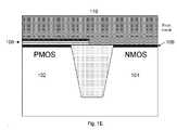
- the well/channel implants 102 (for p-MOS) and 104 (for n-MOS) and isolation steps for both device typesare performed, preferably in accordance with conventional CMOS processing.
- a suitable gate dielectric layer 106is grown/deposited over the active area (Silicon).
- the gate dielectric layer 106may comprise silicon dioxide, silicon nitride, an oxynitride, a silicate, or a high-k material (e.g., hafnium oxide, Hf SiO x N y , aluminum oxide, BST, tantalum pentoxide, or other suitable material).
- two or more thin (10-100 ⁇ ) metal (or metal nitride) layersare deposited over the gate dielectric layer of one of the device types 102 , forming a multi-layer stack 108 .
- Three metal/metal nitride layers 108 a - 108 cform the stack 108 in the illustrated embodiment, although in other embodiments, two layers may be used, as well as four or more layers.
- at least one of the layersis of a different metal/metal nitride type than one of the other layers.
- each of the layerscomprises a different metal/metal nitride type.
- layersconsisting of Ti, Ta, Hf, Nb, Mo, Zr, or W metals/metal nitrides may be used to form the stack 108 .
- These materialsare only exemplary, and those skilled in the art will appreciate that many other conventional thin metals used in the CMOS fabrication process may be used as well.
- Each layer's composition and deposition order in the stack 108is carefully selected in order to produce the final work function requirement of the device type 102 , as will be further described below.
- a thick metal/metal nitride layer 110is deposited.
- This thick metal/metal nitride layer 110may comprise any conventional thick metal/metal nitride films, or alternatively may consist of one of the types used in the multi-layer stack 108 .
- the thick metal/metal nitrideis selected such that it exhibits the desired work function for the second device type 104 (n-MOS).
- the gate electrode 120 for the first device typeincludes a thick metal/metal nitride layer 110 disposed over a stack of two or more thin metal/metal nitride layers 108 a - c , which is disposed over the gate dielectric layer 106 .
- the gate electrode 140 for the second device typecomprises a thick metal/metal nitride layer 110 deposited over the gate dielectric layer 106 .
- the thin metal/metal nitride layers 108 a - cwill typically have an amorphous structure, where as the thick metal/metal nitride layer 110 will typically be in poly crystalline form.
- a change of phase or orientationis known to affect the work function of conducting films. Materials with smaller grain sizes have more grain boundaries and exhibit higher work function values due to the grain boundary effect. In the present case, having 3 metals in the stack impedes with the grain growth during alloying at high temperature and that can result in too many but smaller grains.
- the thin metal/metal nitride layers 108 a - cwill become intermixed during annealing, such intermixing contributing to work function change [I. Polishchuk et al, IEEE EDL 23, p 200, 2002, incorporated herein by reference]. Accordingly, thermal annealing is used in the present invention to promote phase change and intermixing in the thin layers 108 a - c .
- thermal annealingis used in the present invention to promote phase change and intermixing in the thin layers 108 a - c .
- FIGS. 2A-2Cillustrate the work function ( ⁇ m) of gate electrodes 120 and 140 as a function of annealing temperature for exemplary Hf, Ti and Ta materials.
- FIG. 2Athree work function responses are shown, two responses ( 210 and 220 ) showing the work function of gate electrode 120 for two different multi-layer stack compositions, and a third response ( 230 ) for gate electrode 140 which comprises bulk HfN material.
- Response 210shows the work function of gate electrode 120 versus annealing temperature for a multi-layer stack of HfN—Ti—TaN layers, and response 220 for a multi-layer stack of HfN—Ta—TiN.
- FIGS. 2B and 2Cillustrate similar responses for the different compositions of the multi-layer stack 108 and the thick metal/metal nitride layer 110 , as shown.
- the working function of gate electrode 120 comprising the multi-layer Hf, Ti and Ta stackscan be adjusted over a range of approximately 1 eV based upon the annealing temperature chosen.
- the work function for the gate electrode 140 comprising the bulk Hf, Ti and Ta polycrystalline thick metal layerdoes not change significantly after annealing. In this manner, fabrication of gate electrodes having substantially different work functions is realizable using the processes of the present invention.
- the described processesmay be implemented in hardware, software, firmware or a combination of these implementations as appropriate.
- some or all of the described processesmay be implemented as computer readable instruction code resident on a computer readable medium (removable disk, volatile or non-volatile memory, embedded processors, etc.), the instruction code operable to program a computer of other such programmable device to carry out the intended functions.
Landscapes
- Metal-Oxide And Bipolar Metal-Oxide Semiconductor Integrated Circuits (AREA)
- Electrodes Of Semiconductors (AREA)
- Insulated Gate Type Field-Effect Transistor (AREA)
Abstract
Description
- This application claims the benefit of U.S. Provisional Application No. 60/521,649, filed Jun. 10, 2004, the contents of which are hereby incorporated by reference in its entirety for all purposes.
- The present invention relates to semiconductor devices and fabrication processes, and more specifically to semiconductor gate electrode architectures which provide improved work function tuning.
- In the conventional CMOS process, poly silicon is used as a gate electrode material up to 90 nm node. The conventional process has several advantages such as: (i) it is compatible with high temperature processing, (ii) well behaved poly-Si/thermal SiO2interfaces, (iii) more reliable than metal gate electrode like Al, (iv) conformal deposition over steep topography (v) and most significantly it introduces self-aligned dual work function for both n-MOSFETs and p-MOSFETs by selection of proper dopant.
- The polysilicon gate electrode, however, also represents a major challenge for near-term and long-term CMOS scaling. Some major limitations of the process include gate depletion, high gate resistance and boron penetration into the channel region. The poly depletion causes an effective increase in the gate dielectric thickness, which operates to reduce the current drive. Boron diffusion from p+ polysilicon gate to the channel degrades device performance significantly. Both the effective increase in the gate dielectric thickness associated with depletion and the channel autodoping associated with boron out-diffusion from the p+ polysilicon gate will eventually require the phase-out of polysilicon as gate material beyond the 45 nm technology node.
- Metal gate electrodes offer a potential solution to the aforementioned problem. Metal gate electrodes provide advantages such as: (i) no boron penetration from polysilicon gate into channel through very thin gate dielectric, (ii) much lower gate resistance, (iii) and perhaps the most desirable advantage of reduced electrical thickness of gate dielectric. The last and most significant advantage is derived through elimination of depletion in heavily doped polysilicon gates, which can amount to a 3-5 Å reduction in equivalent oxide thickness (EOT)—the equivalent of ˜2 generation advancement.
- A key requirement for gate electrode material in CMOS is that of dual work function. Gate metal for NMOS and PMOS devices should have work functions which closely correspond to conduction and valence band edge respectively for surface channel mode of operation. In conventionally fabricated CMOS devices, the dual work function of the polysilicon gate is achieved by implanting the polysilicon material with either n or p-type dopants (during deep S/D implantation) as mentioned above.
- In the case of refractory metals or metal nitrides, work function is not a strong function of doping, and S/D implantation cannot be used for work function tuning. Further, conventional approaches of using two different bulk metals to fabricate NMOS and PMOS gate electrodes require the use of exotic metals and alloys to meet the work function requirements, which complicates CMOS processing and results in lower device yield.
- What is needed is a gate electrode architecture capable of a dual work function, and which can be preferably fabricated using technology close to conventional CMOS fabrication.
- A method of forming gate electrodes having different work functions includes forming a first well of a first conductivity type and a second well of a second conductivity type. Subsequently, a gate dielectric layer is deposited over at least a portion of the first and second wells. A multi-layer stack comprising two or more thin metal/metal nitride layers is next formed over the first well. A thick metal/metal nitride layer is formed over the multi-layer stack to form the first gate electrode. The thick metal/metal nitride layer is also formed over the gate dielectric layer portion extending over the second well, thereby forming the second gate electrode. The first and second electrodes are then annealed, and thereafter exhibit different work functions as desired.
FIGS. 1A-1G illustrate the processes for fabricating the gate electrode in accordance with one embodiment of the present invention.FIGS. 2A-2C illustrate a working function φm of gate electrodes as a function of annealing temperature for exemplary Hf, Ti, and Ta materials- For clarity, previously identified features retain their reference indicia in subsequent drawings.
- The present invention provides a gate electrode architecture which possesses a dual work function capability and which can be either fabricated using conventional CMOS technology or more futuristic replacement gate approach.
FIGS. 1A-1G illustrate the processes for fabricating the gate electrode architecture in accordance with one embodiment of the present invention. Initially, the well/channel implants102 (for p-MOS) and104 (for n-MOS) and isolation steps for both device types are performed, preferably in accordance with conventional CMOS processing. Next, a suitable gatedielectric layer 106 is grown/deposited over the active area (Silicon). The gatedielectric layer 106 may comprise silicon dioxide, silicon nitride, an oxynitride, a silicate, or a high-k material (e.g., hafnium oxide, Hf SiOxNy, aluminum oxide, BST, tantalum pentoxide, or other suitable material).- Next, two or more thin (10-100 Å) metal (or metal nitride) layers are deposited over the gate dielectric layer of one of the
device types 102, forming amulti-layer stack 108. Three metal/metal nitride layers 108a-108cform thestack 108 in the illustrated embodiment, although in other embodiments, two layers may be used, as well as four or more layers. In the preferred embodiment, at least one of the layers is of a different metal/metal nitride type than one of the other layers. In a further specific embodiment, each of the layers comprises a different metal/metal nitride type. For example, layers consisting of Ti, Ta, Hf, Nb, Mo, Zr, or W metals/metal nitrides may be used to form thestack 108. These materials are only exemplary, and those skilled in the art will appreciate that many other conventional thin metals used in the CMOS fabrication process may be used as well. Each layer's composition and deposition order in thestack 108 is carefully selected in order to produce the final work function requirement of thedevice type 102, as will be further described below. - Next, mask and etch processes are used to remove the
multi-layer stack 108 from the area of thesecond device type 104, a process which is preferably performed using any of the conventional CMOS techniques. Subsequently, a thick metal/metal nitride layer 110 is deposited. This thick metal/metal nitride layer 110 may comprise any conventional thick metal/metal nitride films, or alternatively may consist of one of the types used in themulti-layer stack 108. The thick metal/metal nitride is selected such that it exhibits the desired work function for the second device type104 (n-MOS). At the conclusion of the fabrication process, thegate electrode 120 for the first device type includes a thick metal/metal nitride layer 110 disposed over a stack of two or more thin metal/metal nitride layers 108a-c, which is disposed over the gatedielectric layer 106. Thegate electrode 140 for the second device type comprises a thick metal/metal nitride layer 110 deposited over the gatedielectric layer 106. - Prior to annealing, the thin metal/
metal nitride layers 108a-cwill typically have an amorphous structure, where as the thick metal/metal nitride layer 110 will typically be in poly crystalline form. As is known in the art [H. B. Michaelson, J. Appl. Phys. 48, p 4729, 1977, incorporated herein by reference], a change of phase or orientation is known to affect the work function of conducting films. Materials with smaller grain sizes have more grain boundaries and exhibit higher work function values due to the grain boundary effect. In the present case, having 3 metals in the stack impedes with the grain growth during alloying at high temperature and that can result in too many but smaller grains. It is further known that the thin metal/metal nitride layers 108a-cwill become intermixed during annealing, such intermixing contributing to work function change [I. Polishchuk et al, IEEE EDL 23, p 200, 2002, incorporated herein by reference]. Accordingly, thermal annealing is used in the present invention to promote phase change and intermixing in thethin layers 108a-c. Thus by selecting the composition and number of thethin layers 108a-c, and the annealing temperature, the desired work function can be obtained. FIGS. 2A-2C illustrate the work function (φm) ofgate electrodes FIG. 2A , three work function responses are shown, two responses (210 and220) showing the work function ofgate electrode 120 for two different multi-layer stack compositions, and a third response (230) forgate electrode 140 which comprises bulk HfN material.Response 210 shows the work function ofgate electrode 120 versus annealing temperature for a multi-layer stack of HfN—Ti—TaN layers, andresponse 220 for a multi-layer stack of HfN—Ta—TiN.FIGS. 2B and 2C illustrate similar responses for the different compositions of themulti-layer stack 108 and the thick metal/metal nitride layer 110, as shown.- As can be observed from
FIGS. 2A-2C , the working function ofgate electrode 120 comprising the multi-layer Hf, Ti and Ta stacks can be adjusted over a range of approximately 1 eV based upon the annealing temperature chosen. The work function for thegate electrode 140 comprising the bulk Hf, Ti and Ta polycrystalline thick metal layer does not change significantly after annealing. In this manner, fabrication of gate electrodes having substantially different work functions is realizable using the processes of the present invention. - As readily appreciated by those skilled in the art, the described processes may be implemented in hardware, software, firmware or a combination of these implementations as appropriate. In addition, some or all of the described processes may be implemented as computer readable instruction code resident on a computer readable medium (removable disk, volatile or non-volatile memory, embedded processors, etc.), the instruction code operable to program a computer of other such programmable device to carry out the intended functions.
- The foregoing description has been presented for purposes of illustration and description. It is not intended to be exhaustive or to limit the invention to the precise form disclosed, and obviously many modifications and variations are possible in light of the disclosed teaching. The described embodiments were chosen in order to best explain the principles of the invention and its practical application to thereby enable others skilled in the art to best utilize the invention in various embodiments and with various modifications as are suited to the particular use contemplated. It is intended that the scope of the invention be defined by the claims appended hereto.
Claims (20)
1. A method for fabricating a first gate electrode having a first working function and a second gate electrode having a second working function, the method comprising:
forming a first well of a first conductivity type and a second well of a second conductivity type;
depositing a gate dielectric layer over at least a portion of the first and second wells;
forming a multi-layer stack over the dielectric layer which extends over the first well, the multi-layer stack comprising two or more thin metal/metal nitride layers;
depositing a thick metal/metal nitride layer over (i) the multi-layer stack to form the first gate electrode, and (ii) the gate dielectric layer portion which extends over the second well to form the second gate electrode; and
annealing the first and second gate electrodes.
2. The method ofclaim 1 , further comprising removing the multi-layer stack from the area of the second well.
3. The method ofclaim 1 , wherein annealing the first and second gate electrodes comprises thermal annealing.
4. The method ofclaim 1 , wherein the thin metal/metal nitride layers comprises a metal or metal nitride from the group consisting of Ti, Ta, Hf, Nb, Mo, Zr, and W and their nitrides.
5. The method ofclaim 1 , wherein the thick metal/metal nitride comprises a metal/metal nitride from the group consisting of Ti, Ta, Hf, Nb, Mo, Zr and W and their nitrides.
6. The method ofclaim 1 , wherein the multi-stack comprises three thin metal/metal nitride layers.
7. The method ofclaim 1 , wherein the gate dielectric layer comprises material from the group consisting of silicon dioxide, silicon nitride, oxynitride, silicate, hafnium oxide, aluminum oxide, BST, and tantalum pentoxide.
8. A semiconductor device having a first well of a first conductivity type and a second well of a second conductivity type, the semiconductor device comprising:
a gate dielectric layer extending over at least a portion of the first well and the second well;
a first gate electrode disposed on the gate dielectric layer and extending over the first well, the first gate electrode comprising a multi-layer stack, comprising:
(i) a first thin metal/metal nitride layer disposed on the gate dielectric layer;
(ii) a second thin metal/metal nitride layer disposed on the first thin metal/metal nitride layer;
(iii) a third thin metal/metal nitride layer disposed on the second thin metal/metal nitride layer; and
(iv) a first thick metal/metal nitride layer disposed on the third thin metal/metal nitride layer
a first source electrode and a first drain electrode formed in the first well adjacent to the first gate electrode;
a second gate electrode disposed on the gate dielectric layer and extending over the second well, the second gate electrode comprising a portion of the first thick metal/metal nitride layer; and
a second source electrode and a second drain electrode formed in the second well adjacent to the second gate electrode.
9. The semiconductor device ofclaim 8 , wherein, after annealing, the multi-layer stack comprises a first work function voltage, and after annealing, the annealed thick metal/metal nitride layer comprises a second, different work function voltage.
10. The semiconductor device ofclaim 8 , wherein the first, second, and third thin metal/metal nitride layers comprise of amorphous or polycrystalline form as deposited, and a changed microstructure when annealed.
11. The semiconductor device ofclaim 8 , wherein the first thick metal/metal nitride layer comprise a poly crystalline structure as deposited.
12. The semiconductor ofclaim 8 , wherein the thickness of each of the first, second, and third thin metal/metal nitride layers is 10-100 Angstroms.
13. A computer program product, resident on a computer readable medium operable to control a system to fabricate a first gate electrode having a first working function and a second gate electrode having a second working function, the computer program product comprising:
instruction code to form a first well of a first conductivity type and a second well of a second conductivity type;
instruction code to deposit a gate dielectric layer over at least a portion of the first and second wells;
instruction code to form a multi-layer stack over the dielectric layer which extends over the first well, the multi-layer stack comprising two or more thin metal/metal nitride layers;
instruction code to deposit a thick metal/metal nitride layer over (i) the multi-layer stack to form the first gate electrode, and (ii) the gate dielectric layer portion which extends over the second well to form the second gate electrode; and
instruction code to anneal the first and second gate electrodes.
14. The computer program product ofclaim 13 , further comprising instruction code to remove the multi-layer stack from the area of the second well.
15. The computer program product ofclaim 13 , wherein the instruction code to anneal the first and second gate electrodes comprises instruction code to thermally anneal the first and second gate electrodes.
16. The computer program product ofclaim 13 , wherein the thin metal/metal nitride layers comprises a metal or metal nitride from the group consisting of Ti, Ta, Hf, Nb, Mo, Zr, and W and their nitrides.
17. The computer program product ofclaim 13 , wherein the thick metal/metal nitride comprises a metal/metal nitride from the group consisting of Ti, Ta, Hf, Nb, Mo, Zr and W and their nitrides.
18. The computer program product ofclaim 13 , wherein the multi-stack comprises three thin metal/metal nitride layers.
19. The computer program product ofclaim 13 , wherein the gate dielectric layer comprises material from the group consisting of silicon dioxide, silicon nitride, oxynitride, silicate, hafnium oxide, aluminum oxide, BST, and tantalum pentoxide.
20. A semiconductor device having a first well of a first conductivity type and a second well of a second conductivity type, the semiconductor device comprising:
gate dielectric layer means extending over at least a portion of the first well and the second well;
first gate electrode means disposed on the gate dielectric layer means and extending over the first well, the first gate electrode means comprising a multi-layer stack, comprising:
(i) a first thin metal/metal nitride layer disposed on the gate dielectric layer;
(ii) a second thin metal/metal nitride layer disposed on the first thin metal/metal nitride layer;
(iii) a third thin metal/metal nitride layer disposed on the second thin metal/metal nitride layer; and
(iv) a first thick metal/metal nitride layer disposed on the third thin metal/metal nitride layer
first source electrode means and first drain electrode means formed in the first well adjacent to the first gate electrode means;
second gate electrode means disposed on the gate dielectric layer and extending over the second well, the second gate electrode means comprising a portion of the first thick metal/metal nitride layer; and
second source electrode means and second drain electrode means formed in the second well adjacent to the second gate electrode means.
Priority Applications (1)
| Application Number | Priority Date | Filing Date | Title |
|---|---|---|---|
| US11/160,126US7397090B2 (en) | 2004-06-10 | 2005-06-09 | Gate electrode architecture for improved work function tuning and method of manufacture |
Applications Claiming Priority (2)
| Application Number | Priority Date | Filing Date | Title |
|---|---|---|---|
| US52164904P | 2004-06-10 | 2004-06-10 | |
| US11/160,126US7397090B2 (en) | 2004-06-10 | 2005-06-09 | Gate electrode architecture for improved work function tuning and method of manufacture |
Publications (2)
| Publication Number | Publication Date |
|---|---|
| US20050275035A1true US20050275035A1 (en) | 2005-12-15 |
| US7397090B2 US7397090B2 (en) | 2008-07-08 |
Family
ID=35459636
Family Applications (1)
| Application Number | Title | Priority Date | Filing Date |
|---|---|---|---|
| US11/160,126Expired - Fee RelatedUS7397090B2 (en) | 2004-06-10 | 2005-06-09 | Gate electrode architecture for improved work function tuning and method of manufacture |
Country Status (1)
| Country | Link |
|---|---|
| US (1) | US7397090B2 (en) |
Cited By (46)
| Publication number | Priority date | Publication date | Assignee | Title |
|---|---|---|---|---|
| US20070004224A1 (en)* | 2005-06-29 | 2007-01-04 | Amberwave Systems Corporation | Methods for forming dielectrics and metal electrodes |
| US20070001231A1 (en)* | 2005-06-29 | 2007-01-04 | Amberwave Systems Corporation | Material systems for dielectrics and metal electrodes |
| US20070015325A1 (en)* | 2005-07-14 | 2007-01-18 | Matthias Goldbach | Manufacturing method for an integrated semiconductor structure and corresponding integrated semiconductor structure |
| US20080242070A1 (en)* | 2007-03-30 | 2008-10-02 | International Business Machines Corporation | Integration schemes for fabricating polysilicon gate mosfet and high-k dielectric metal gate mosfet |
| US20080272435A1 (en)* | 2007-05-02 | 2008-11-06 | Chien-Ting Lin | Semiconductor device and method of forming the same |
| US8211775B1 (en) | 2011-03-09 | 2012-07-03 | United Microelectronics Corp. | Method of making transistor having metal gate |
| US8324118B2 (en) | 2011-03-28 | 2012-12-04 | United Microelectronics Corp. | Manufacturing method of metal gate structure |
| US8329597B2 (en) | 2011-03-07 | 2012-12-11 | United Microelectronics Corp. | Semiconductor process having dielectric layer including metal oxide and MOS transistor process |
| US8426277B2 (en) | 2011-09-23 | 2013-04-23 | United Microelectronics Corp. | Semiconductor process |
| US8440511B1 (en) | 2011-11-16 | 2013-05-14 | United Microelectronics Corp. | Method for manufacturing multi-gate transistor device |
| US8486790B2 (en) | 2011-07-18 | 2013-07-16 | United Microelectronics Corp. | Manufacturing method for metal gate |
| US8501636B1 (en) | 2012-07-24 | 2013-08-06 | United Microelectronics Corp. | Method for fabricating silicon dioxide layer |
| US8501634B2 (en) | 2011-03-10 | 2013-08-06 | United Microelectronics Corp. | Method for fabricating gate structure |
| US8519487B2 (en) | 2011-03-21 | 2013-08-27 | United Microelectronics Corp. | Semiconductor device |
| US8530980B2 (en) | 2011-04-27 | 2013-09-10 | United Microelectronics Corp. | Gate stack structure with etch stop layer and manufacturing process thereof |
| US8536038B2 (en) | 2011-06-21 | 2013-09-17 | United Microelectronics Corp. | Manufacturing method for metal gate using ion implantation |
| US8551876B2 (en) | 2011-08-18 | 2013-10-08 | United Microelectronics Corp. | Manufacturing method for semiconductor device having metal gate |
| US8642457B2 (en) | 2011-03-03 | 2014-02-04 | United Microelectronics Corp. | Method of fabricating semiconductor device |
| US8673758B2 (en) | 2011-06-16 | 2014-03-18 | United Microelectronics Corp. | Structure of metal gate and fabrication method thereof |
| US8691681B2 (en) | 2012-01-04 | 2014-04-08 | United Microelectronics Corp. | Semiconductor device having a metal gate and fabricating method thereof |
| US20140124876A1 (en)* | 2012-11-06 | 2014-05-08 | GlobalFoundries, Inc. | Metal gate structure for midgap semiconductor device and method of making same |
| US8735269B1 (en) | 2013-01-15 | 2014-05-27 | United Microelectronics Corp. | Method for forming semiconductor structure having TiN layer |
| US8802579B2 (en) | 2011-10-12 | 2014-08-12 | United Microelectronics Corp. | Semiconductor structure and fabrication method thereof |
| US8841733B2 (en) | 2011-05-17 | 2014-09-23 | United Microelectronics Corp. | Semiconductor device and method of fabricating the same |
| US8860181B2 (en) | 2012-03-07 | 2014-10-14 | United Microelectronics Corp. | Thin film resistor structure |
| US8872286B2 (en) | 2011-08-22 | 2014-10-28 | United Microelectronics Corp. | Metal gate structure and fabrication method thereof |
| US8921947B1 (en) | 2013-06-10 | 2014-12-30 | United Microelectronics Corp. | Multi-metal gate semiconductor device having triple diameter metal opening |
| US8921238B2 (en) | 2011-09-19 | 2014-12-30 | United Microelectronics Corp. | Method for processing high-k dielectric layer |
| US8951884B1 (en) | 2013-11-14 | 2015-02-10 | United Microelectronics Corp. | Method for forming a FinFET structure |
| US20150048486A1 (en)* | 2013-08-15 | 2015-02-19 | United Microelectronics Corporation | Spatial semiconductor structure and method of fabricating the same |
| US8975666B2 (en) | 2012-08-22 | 2015-03-10 | United Microelectronics Corp. | MOS transistor and process thereof |
| US8987096B2 (en) | 2012-02-07 | 2015-03-24 | United Microelectronics Corp. | Semiconductor process |
| US9000568B2 (en) | 2011-09-26 | 2015-04-07 | United Microelectronics Corp. | Semiconductor structure and fabrication method thereof |
| US9054172B2 (en) | 2012-12-05 | 2015-06-09 | United Microelectrnics Corp. | Semiconductor structure having contact plug and method of making the same |
| US9105720B2 (en) | 2013-09-11 | 2015-08-11 | United Microelectronics Corp. | Semiconductor device having metal gate and manufacturing method thereof |
| US9105623B2 (en) | 2012-05-25 | 2015-08-11 | United Microelectronics Corp. | Semiconductor device having metal gate and manufacturing method thereof |
| US9117878B2 (en) | 2012-12-11 | 2015-08-25 | United Microelectronics Corp. | Method for manufacturing shallow trench isolation |
| US9159798B2 (en) | 2013-05-03 | 2015-10-13 | United Microelectronics Corp. | Replacement gate process and device manufactured using the same |
| US9196546B2 (en) | 2013-09-13 | 2015-11-24 | United Microelectronics Corp. | Metal gate transistor |
| US9196542B2 (en) | 2013-05-22 | 2015-11-24 | United Microelectronics Corp. | Method for manufacturing semiconductor devices |
| US9231071B2 (en) | 2014-02-24 | 2016-01-05 | United Microelectronics Corp. | Semiconductor structure and manufacturing method of the same |
| US9384962B2 (en) | 2011-04-07 | 2016-07-05 | United Microelectronics Corp. | Oxygen treatment of replacement work-function metals in CMOS transistor gates |
| US9406516B2 (en) | 2013-09-11 | 2016-08-02 | United Microelectronics Corp. | High-K metal gate process for lowering junction leakage and interface traps in NMOS transistor |
| US9478627B2 (en) | 2012-05-18 | 2016-10-25 | United Microelectronics Corp. | Semiconductor structure and process thereof |
| US9490342B2 (en) | 2011-06-16 | 2016-11-08 | United Microelectronics Corp. | Method for fabricating semiconductor device |
| US9653300B2 (en) | 2013-04-16 | 2017-05-16 | United Microelectronics Corp. | Structure of metal gate structure and manufacturing method of the same |
Families Citing this family (3)
| Publication number | Priority date | Publication date | Assignee | Title |
|---|---|---|---|---|
| JP4963021B2 (en)* | 2005-09-06 | 2012-06-27 | 独立行政法人産業技術総合研究所 | Semiconductor structure |
| US8129280B2 (en)* | 2009-07-24 | 2012-03-06 | Applied Materials, Inc. | Substrate device having a tuned work function and methods of forming thereof |
| US9105577B2 (en) | 2012-02-16 | 2015-08-11 | International Business Machines Corporation | MOSFET with work function adjusted metal backgate |
Citations (9)
| Publication number | Priority date | Publication date | Assignee | Title |
|---|---|---|---|---|
| US6291282B1 (en)* | 1999-02-26 | 2001-09-18 | Texas Instruments Incorporated | Method of forming dual metal gate structures or CMOS devices |
| US6373111B1 (en)* | 1999-11-30 | 2002-04-16 | Intel Corporation | Work function tuning for MOSFET gate electrodes |
| US6458695B1 (en)* | 2001-10-18 | 2002-10-01 | Chartered Semiconductor Manufacturing Ltd. | Methods to form dual metal gates by incorporating metals and their conductive oxides |
| US20020151125A1 (en)* | 2001-04-11 | 2002-10-17 | Samsung Electronics Co., Ltd. | Method of forming a CMOS type semiconductor device having dual gates |
| US6492217B1 (en)* | 1998-06-30 | 2002-12-10 | Intel Corporation | Complementary metal gates and a process for implementation |
| US6514827B2 (en)* | 2000-12-29 | 2003-02-04 | Hynix Semiconductor Inc. | Method for fabricating a dual metal gate for a semiconductor device |
| US6545324B2 (en)* | 2000-06-12 | 2003-04-08 | Motorola, Inc. | Dual metal gate transistors for CMOS process |
| US6809394B1 (en)* | 2003-08-13 | 2004-10-26 | Texas Instruments Incorporated | Dual metal-alloy nitride gate electrodes |
| US20050258468A1 (en)* | 2004-05-24 | 2005-11-24 | Texas Instruments, Incorporated | Dual work function metal gate integration in semiconductor devices |
- 2005
- 2005-06-09USUS11/160,126patent/US7397090B2/ennot_activeExpired - Fee Related
Patent Citations (9)
| Publication number | Priority date | Publication date | Assignee | Title |
|---|---|---|---|---|
| US6492217B1 (en)* | 1998-06-30 | 2002-12-10 | Intel Corporation | Complementary metal gates and a process for implementation |
| US6291282B1 (en)* | 1999-02-26 | 2001-09-18 | Texas Instruments Incorporated | Method of forming dual metal gate structures or CMOS devices |
| US6373111B1 (en)* | 1999-11-30 | 2002-04-16 | Intel Corporation | Work function tuning for MOSFET gate electrodes |
| US6545324B2 (en)* | 2000-06-12 | 2003-04-08 | Motorola, Inc. | Dual metal gate transistors for CMOS process |
| US6514827B2 (en)* | 2000-12-29 | 2003-02-04 | Hynix Semiconductor Inc. | Method for fabricating a dual metal gate for a semiconductor device |
| US20020151125A1 (en)* | 2001-04-11 | 2002-10-17 | Samsung Electronics Co., Ltd. | Method of forming a CMOS type semiconductor device having dual gates |
| US6458695B1 (en)* | 2001-10-18 | 2002-10-01 | Chartered Semiconductor Manufacturing Ltd. | Methods to form dual metal gates by incorporating metals and their conductive oxides |
| US6809394B1 (en)* | 2003-08-13 | 2004-10-26 | Texas Instruments Incorporated | Dual metal-alloy nitride gate electrodes |
| US20050258468A1 (en)* | 2004-05-24 | 2005-11-24 | Texas Instruments, Incorporated | Dual work function metal gate integration in semiconductor devices |
Cited By (67)
| Publication number | Priority date | Publication date | Assignee | Title |
|---|---|---|---|---|
| US20070004224A1 (en)* | 2005-06-29 | 2007-01-04 | Amberwave Systems Corporation | Methods for forming dielectrics and metal electrodes |
| US20070001231A1 (en)* | 2005-06-29 | 2007-01-04 | Amberwave Systems Corporation | Material systems for dielectrics and metal electrodes |
| US7432139B2 (en) | 2005-06-29 | 2008-10-07 | Amberwave Systems Corp. | Methods for forming dielectrics and metal electrodes |
| US7202535B2 (en)* | 2005-07-14 | 2007-04-10 | Infineon Technologies Ag | Manufacturing method for an integrated semiconductor structure and corresponding integrated semiconductor structure |
| US20070187774A1 (en)* | 2005-07-14 | 2007-08-16 | Matthias Goldbach | Manufacturing method for an integrated semiconductor structure and corresponding integrated semiconductor structure |
| US20070015325A1 (en)* | 2005-07-14 | 2007-01-18 | Matthias Goldbach | Manufacturing method for an integrated semiconductor structure and corresponding integrated semiconductor structure |
| US20080242070A1 (en)* | 2007-03-30 | 2008-10-02 | International Business Machines Corporation | Integration schemes for fabricating polysilicon gate mosfet and high-k dielectric metal gate mosfet |
| US7435652B1 (en)* | 2007-03-30 | 2008-10-14 | International Business Machines Corporation | Integration schemes for fabricating polysilicon gate MOSFET and high-K dielectric metal gate MOSFET |
| US20080272435A1 (en)* | 2007-05-02 | 2008-11-06 | Chien-Ting Lin | Semiconductor device and method of forming the same |
| US20080318371A1 (en)* | 2007-05-02 | 2008-12-25 | Chien-Ting Lin | Semiconductor device and method of forming the same |
| US7759202B2 (en) | 2007-05-02 | 2010-07-20 | United Microelectronics Corp. | Method for forming semiconductor device with gates of different materials |
| US8642457B2 (en) | 2011-03-03 | 2014-02-04 | United Microelectronics Corp. | Method of fabricating semiconductor device |
| US8329597B2 (en) | 2011-03-07 | 2012-12-11 | United Microelectronics Corp. | Semiconductor process having dielectric layer including metal oxide and MOS transistor process |
| US8211775B1 (en) | 2011-03-09 | 2012-07-03 | United Microelectronics Corp. | Method of making transistor having metal gate |
| US8501634B2 (en) | 2011-03-10 | 2013-08-06 | United Microelectronics Corp. | Method for fabricating gate structure |
| US8519487B2 (en) | 2011-03-21 | 2013-08-27 | United Microelectronics Corp. | Semiconductor device |
| US8723274B2 (en) | 2011-03-21 | 2014-05-13 | United Microelectronics Corp. | Semiconductor device and method for fabricating the same |
| US8324118B2 (en) | 2011-03-28 | 2012-12-04 | United Microelectronics Corp. | Manufacturing method of metal gate structure |
| US9384962B2 (en) | 2011-04-07 | 2016-07-05 | United Microelectronics Corp. | Oxygen treatment of replacement work-function metals in CMOS transistor gates |
| US9087782B2 (en) | 2011-04-27 | 2015-07-21 | United Microelectronics Corporation | Manufacturing process of gate stack structure with etch stop layer |
| US8530980B2 (en) | 2011-04-27 | 2013-09-10 | United Microelectronics Corp. | Gate stack structure with etch stop layer and manufacturing process thereof |
| US9190292B2 (en) | 2011-04-27 | 2015-11-17 | United Microelectronics Corporation | Manufacturing process of gate stack structure with etch stop layer |
| US8841733B2 (en) | 2011-05-17 | 2014-09-23 | United Microelectronics Corp. | Semiconductor device and method of fabricating the same |
| US9130032B2 (en) | 2011-05-17 | 2015-09-08 | United Microelectronics Corp. | Semiconductor device |
| US8673758B2 (en) | 2011-06-16 | 2014-03-18 | United Microelectronics Corp. | Structure of metal gate and fabrication method thereof |
| US9490342B2 (en) | 2011-06-16 | 2016-11-08 | United Microelectronics Corp. | Method for fabricating semiconductor device |
| US8536038B2 (en) | 2011-06-21 | 2013-09-17 | United Microelectronics Corp. | Manufacturing method for metal gate using ion implantation |
| US8486790B2 (en) | 2011-07-18 | 2013-07-16 | United Microelectronics Corp. | Manufacturing method for metal gate |
| US8551876B2 (en) | 2011-08-18 | 2013-10-08 | United Microelectronics Corp. | Manufacturing method for semiconductor device having metal gate |
| US9281374B2 (en) | 2011-08-22 | 2016-03-08 | United Microelectronics Corp. | Metal gate structure and fabrication method thereof |
| US8872286B2 (en) | 2011-08-22 | 2014-10-28 | United Microelectronics Corp. | Metal gate structure and fabrication method thereof |
| US8921238B2 (en) | 2011-09-19 | 2014-12-30 | United Microelectronics Corp. | Method for processing high-k dielectric layer |
| US8426277B2 (en) | 2011-09-23 | 2013-04-23 | United Microelectronics Corp. | Semiconductor process |
| US9000568B2 (en) | 2011-09-26 | 2015-04-07 | United Microelectronics Corp. | Semiconductor structure and fabrication method thereof |
| US8802579B2 (en) | 2011-10-12 | 2014-08-12 | United Microelectronics Corp. | Semiconductor structure and fabrication method thereof |
| US8440511B1 (en) | 2011-11-16 | 2013-05-14 | United Microelectronics Corp. | Method for manufacturing multi-gate transistor device |
| US8691681B2 (en) | 2012-01-04 | 2014-04-08 | United Microelectronics Corp. | Semiconductor device having a metal gate and fabricating method thereof |
| US9018086B2 (en) | 2012-01-04 | 2015-04-28 | United Microelectronics Corp. | Semiconductor device having a metal gate and fabricating method thereof |
| US8987096B2 (en) | 2012-02-07 | 2015-03-24 | United Microelectronics Corp. | Semiconductor process |
| US8860181B2 (en) | 2012-03-07 | 2014-10-14 | United Microelectronics Corp. | Thin film resistor structure |
| US10199277B2 (en) | 2012-05-18 | 2019-02-05 | United Microelectronics Corp. | Semiconductor process |
| US9478627B2 (en) | 2012-05-18 | 2016-10-25 | United Microelectronics Corp. | Semiconductor structure and process thereof |
| US9105623B2 (en) | 2012-05-25 | 2015-08-11 | United Microelectronics Corp. | Semiconductor device having metal gate and manufacturing method thereof |
| US8501636B1 (en) | 2012-07-24 | 2013-08-06 | United Microelectronics Corp. | Method for fabricating silicon dioxide layer |
| US8975666B2 (en) | 2012-08-22 | 2015-03-10 | United Microelectronics Corp. | MOS transistor and process thereof |
| US20140124876A1 (en)* | 2012-11-06 | 2014-05-08 | GlobalFoundries, Inc. | Metal gate structure for midgap semiconductor device and method of making same |
| US9496143B2 (en)* | 2012-11-06 | 2016-11-15 | Globalfoundries Inc. | Metal gate structure for midgap semiconductor device and method of making same |
| CN103811326A (en)* | 2012-11-06 | 2014-05-21 | 格罗方德半导体公司 | Metal gate structure for midgap semiconductor device and method of making same |
| US9054172B2 (en) | 2012-12-05 | 2015-06-09 | United Microelectrnics Corp. | Semiconductor structure having contact plug and method of making the same |
| US9281367B2 (en) | 2012-12-05 | 2016-03-08 | United Microelectronics Corp. | Semiconductor structure having contact plug and method of making the same |
| US10049929B2 (en) | 2012-12-05 | 2018-08-14 | United Microelectronics Corp. | Method of making semiconductor structure having contact plug |
| US9117878B2 (en) | 2012-12-11 | 2015-08-25 | United Microelectronics Corp. | Method for manufacturing shallow trench isolation |
| US8735269B1 (en) | 2013-01-15 | 2014-05-27 | United Microelectronics Corp. | Method for forming semiconductor structure having TiN layer |
| US9653300B2 (en) | 2013-04-16 | 2017-05-16 | United Microelectronics Corp. | Structure of metal gate structure and manufacturing method of the same |
| US10199228B2 (en) | 2013-04-16 | 2019-02-05 | United Microelectronics Corp. | Manufacturing method of metal gate structure |
| US9159798B2 (en) | 2013-05-03 | 2015-10-13 | United Microelectronics Corp. | Replacement gate process and device manufactured using the same |
| US9196542B2 (en) | 2013-05-22 | 2015-11-24 | United Microelectronics Corp. | Method for manufacturing semiconductor devices |
| US8921947B1 (en) | 2013-06-10 | 2014-12-30 | United Microelectronics Corp. | Multi-metal gate semiconductor device having triple diameter metal opening |
| US9105582B2 (en)* | 2013-08-15 | 2015-08-11 | United Microelectronics Corporation | Spatial semiconductor structure and method of fabricating the same |
| US20150048486A1 (en)* | 2013-08-15 | 2015-02-19 | United Microelectronics Corporation | Spatial semiconductor structure and method of fabricating the same |
| US9362358B2 (en) | 2013-08-15 | 2016-06-07 | United Microelectronics Corporation | Spatial semiconductor structure |
| US9406516B2 (en) | 2013-09-11 | 2016-08-02 | United Microelectronics Corp. | High-K metal gate process for lowering junction leakage and interface traps in NMOS transistor |
| US9105720B2 (en) | 2013-09-11 | 2015-08-11 | United Microelectronics Corp. | Semiconductor device having metal gate and manufacturing method thereof |
| US9825144B2 (en) | 2013-09-13 | 2017-11-21 | United Microelectronics Corp. | Semiconductor device having metal gate structure |
| US9196546B2 (en) | 2013-09-13 | 2015-11-24 | United Microelectronics Corp. | Metal gate transistor |
| US8951884B1 (en) | 2013-11-14 | 2015-02-10 | United Microelectronics Corp. | Method for forming a FinFET structure |
| US9231071B2 (en) | 2014-02-24 | 2016-01-05 | United Microelectronics Corp. | Semiconductor structure and manufacturing method of the same |
Also Published As
| Publication number | Publication date |
|---|---|
| US7397090B2 (en) | 2008-07-08 |
Similar Documents
| Publication | Publication Date | Title |
|---|---|---|
| US7397090B2 (en) | Gate electrode architecture for improved work function tuning and method of manufacture | |
| US11031482B2 (en) | Gate electrode having a capping layer | |
| JP5336857B2 (en) | Method for changing work function of conductive electrode by introducing metal impurity (and semiconductor structure thereof) | |
| JP6218384B2 (en) | Manufacturing method of semiconductor device having tungsten gate electrode | |
| US7824990B2 (en) | Multi-metal-oxide high-K gate dielectrics | |
| TWI427770B (en) | Technology for stacking high-k metal gates to enable multiple constant voltage devices | |
| US7547951B2 (en) | Semiconductor devices having nitrogen-incorporated active region and methods of fabricating the same | |
| TWI512979B (en) | Field effect transistor device for metal gate stack of oxygen barrier layer | |
| DE102012209512B4 (en) | Metal gate stacking in exchange gate technology | |
| US7387956B2 (en) | Refractory metal-based electrodes for work function setting in semiconductor devices | |
| TWI397962B (en) | Semiconductor structure and method of forming same | |
| US8053300B2 (en) | Semiconductor device | |
| US9577057B2 (en) | Semiconductor device contacts | |
| CN100452357C (en) | Semiconductor device and manufacturing method thereof | |
| CN103500732B (en) | The manufacture method of semiconductor device and semiconductor device | |
| US20120104506A1 (en) | Cmosfet device with controlled threshold voltage characteristics and method of fabricating the same | |
| JP2011187478A (en) | Semiconductor device and method of manufacturing the same | |
| US20070200160A1 (en) | Semiconductor device and method of fabricating the same | |
| JP2007534148A (en) | Method and apparatus for manufacturing a CMOS field effect transistor | |
| EP2294609B1 (en) | Interfacial layer regrowth control in high-k gate structure for field effect transistor | |
| US7018883B2 (en) | Dual work function gate electrodes |
Legal Events
| Date | Code | Title | Description |
|---|---|---|---|
| AS | Assignment | Owner name:AGENCY FOR SCIENCE, TECHNOLOGY AND RESEARCH, SINGA Free format text:ASSIGNMENT OF ASSIGNORS INTEREST;ASSIGNORS:MATHEW, SHAJAN;BERA, LAKSHMI KANTA;BALASUBRAMANIAN, NARAYANAN;REEL/FRAME:016462/0663;SIGNING DATES FROM 20050822 TO 20050823 | |
| FPAY | Fee payment | Year of fee payment:4 | |
| REMI | Maintenance fee reminder mailed | ||
| LAPS | Lapse for failure to pay maintenance fees | ||
| STCH | Information on status: patent discontinuation | Free format text:PATENT EXPIRED DUE TO NONPAYMENT OF MAINTENANCE FEES UNDER 37 CFR 1.362 | |
| FP | Lapsed due to failure to pay maintenance fee | Effective date:20160708 |