US20050275010A1 - Semiconductor nano-wire devices and methods of fabrication - Google Patents
Semiconductor nano-wire devices and methods of fabricationDownload PDFInfo
- Publication number
- US20050275010A1 US20050275010A1US11/104,348US10434805AUS2005275010A1US 20050275010 A1US20050275010 A1US 20050275010A1US 10434805 AUS10434805 AUS 10434805AUS 2005275010 A1US2005275010 A1US 2005275010A1
- Authority
- US
- United States
- Prior art keywords
- annealing
- region
- patterned mask
- nano
- silicon
- Prior art date
- Legal status (The legal status is an assumption and is not a legal conclusion. Google has not performed a legal analysis and makes no representation as to the accuracy of the status listed.)
- Granted
Links
- 238000000034methodMethods0.000titleclaimsabstractdescription69
- 239000002070nanowireSubstances0.000titleclaimsabstractdescription62
- 239000004065semiconductorSubstances0.000titleclaimsdescription66
- 238000004519manufacturing processMethods0.000titleclaimsdescription10
- XUIMIQQOPSSXEZ-UHFFFAOYSA-NSiliconChemical group[Si]XUIMIQQOPSSXEZ-UHFFFAOYSA-N0.000claimsabstractdescription72
- 229910052710siliconInorganic materials0.000claimsabstractdescription60
- 239000010703siliconSubstances0.000claimsabstractdescription53
- 238000000137annealingMethods0.000claimsabstractdescription40
- VYPSYNLAJGMNEJ-UHFFFAOYSA-NSilicium dioxideChemical compoundO=[Si]=OVYPSYNLAJGMNEJ-UHFFFAOYSA-N0.000claimsabstractdescription13
- 230000000873masking effectEffects0.000claimsabstractdescription8
- 230000008569processEffects0.000claimsdescription24
- UFHFLCQGNIYNRP-UHFFFAOYSA-NHydrogenChemical group[H][H]UFHFLCQGNIYNRP-UHFFFAOYSA-N0.000claimsdescription13
- 239000001257hydrogenSubstances0.000claimsdescription11
- 229910052739hydrogenInorganic materials0.000claimsdescription11
- IJGRMHOSHXDMSA-UHFFFAOYSA-NAtomic nitrogenChemical compoundN#NIJGRMHOSHXDMSA-UHFFFAOYSA-N0.000claimsdescription8
- 239000012212insulatorSubstances0.000claimsdescription8
- 239000003989dielectric materialSubstances0.000claimsdescription7
- 238000000059patterningMethods0.000claimsdescription7
- 229910052814silicon oxideInorganic materials0.000claimsdescription7
- 238000009966trimmingMethods0.000claimsdescription7
- XKRFYHLGVUSROY-UHFFFAOYSA-NArgonChemical compound[Ar]XKRFYHLGVUSROY-UHFFFAOYSA-N0.000claimsdescription6
- 238000006243chemical reactionMethods0.000claimsdescription6
- 239000007772electrode materialSubstances0.000claimsdescription6
- 239000007789gasSubstances0.000claimsdescription6
- 239000000758substrateSubstances0.000claimsdescription6
- 229910052786argonInorganic materials0.000claimsdescription3
- 239000011261inert gasSubstances0.000claimsdescription3
- 229910052757nitrogenInorganic materials0.000claimsdescription3
- 229910001873dinitrogenInorganic materials0.000claimsdescription2
- 239000011810insulating materialSubstances0.000claimsdescription2
- QJGQUHMNIGDVPM-UHFFFAOYSA-Nnitrogen groupChemical group[N]QJGQUHMNIGDVPM-UHFFFAOYSA-N0.000claims3
- 150000002431hydrogenChemical class0.000claims2
- 230000005012migrationEffects0.000abstractdescription18
- 238000013508migrationMethods0.000abstractdescription18
- 239000000463materialSubstances0.000abstractdescription9
- 239000002071nanotubeSubstances0.000abstractdescription6
- 239000002073nanorodSubstances0.000abstractdescription4
- 239000000377silicon dioxideSubstances0.000abstractdescription3
- 229910052581Si3N4Inorganic materials0.000abstractdescription2
- 235000012239silicon dioxideNutrition0.000abstractdescription2
- HQVNEWCFYHHQES-UHFFFAOYSA-Nsilicon nitrideChemical compoundN12[Si]34N5[Si]62N3[Si]51N64HQVNEWCFYHHQES-UHFFFAOYSA-N0.000abstractdescription2
- 239000010410layerSubstances0.000description53
- 230000000694effectsEffects0.000description10
- 230000015572biosynthetic processEffects0.000description7
- 230000005669field effectEffects0.000description7
- 229910000577Silicon-germaniumInorganic materials0.000description4
- 230000008901benefitEffects0.000description4
- 238000005530etchingMethods0.000description4
- 239000000203mixtureSubstances0.000description4
- KRHYYFGTRYWZRS-UHFFFAOYSA-NFluoraneChemical compoundFKRHYYFGTRYWZRS-UHFFFAOYSA-N0.000description3
- 238000005229chemical vapour depositionMethods0.000description3
- 239000007769metal materialSubstances0.000description3
- 230000001629suppressionEffects0.000description3
- JBRZTFJDHDCESZ-UHFFFAOYSA-NAsGaChemical compound[As]#[Ga]JBRZTFJDHDCESZ-UHFFFAOYSA-N0.000description2
- 229910001218Gallium arsenideInorganic materials0.000description2
- NBIIXXVUZAFLBC-UHFFFAOYSA-NPhosphoric acidChemical compoundOP(O)(O)=ONBIIXXVUZAFLBC-UHFFFAOYSA-N0.000description2
- MCMNRKCIXSYSNV-UHFFFAOYSA-NZirconium dioxideChemical compoundO=[Zr]=OMCMNRKCIXSYSNV-UHFFFAOYSA-N0.000description2
- LEVVHYCKPQWKOP-UHFFFAOYSA-N[Si].[Ge]Chemical compound[Si].[Ge]LEVVHYCKPQWKOP-UHFFFAOYSA-N0.000description2
- 238000005054agglomerationMethods0.000description2
- 230000002776aggregationEffects0.000description2
- 229910045601alloyInorganic materials0.000description2
- 239000000956alloySubstances0.000description2
- 239000004020conductorSubstances0.000description2
- 229910052732germaniumInorganic materials0.000description2
- GNPVGFCGXDBREM-UHFFFAOYSA-Ngermanium atomChemical compound[Ge]GNPVGFCGXDBREM-UHFFFAOYSA-N0.000description2
- 230000006872improvementEffects0.000description2
- 230000003647oxidationEffects0.000description2
- 238000007254oxidation reactionMethods0.000description2
- 238000000206photolithographyMethods0.000description2
- 230000008707rearrangementEffects0.000description2
- 239000007858starting materialSubstances0.000description2
- 229910000530Gallium indium arsenideInorganic materials0.000description1
- GPXJNWSHGFTCBW-UHFFFAOYSA-NIndium phosphideChemical compound[In]#PGPXJNWSHGFTCBW-UHFFFAOYSA-N0.000description1
- ZOKXTWBITQBERF-UHFFFAOYSA-NMolybdenumChemical compound[Mo]ZOKXTWBITQBERF-UHFFFAOYSA-N0.000description1
- RTAQQCXQSZGOHL-UHFFFAOYSA-NTitaniumChemical compound[Ti]RTAQQCXQSZGOHL-UHFFFAOYSA-N0.000description1
- NRTOMJZYCJJWKI-UHFFFAOYSA-NTitanium nitrideChemical compound[Ti]#NNRTOMJZYCJJWKI-UHFFFAOYSA-N0.000description1
- AXQKVSDUCKWEKE-UHFFFAOYSA-N[C].[Ge].[Si]Chemical compound[C].[Ge].[Si]AXQKVSDUCKWEKE-UHFFFAOYSA-N0.000description1
- HMDDXIMCDZRSNE-UHFFFAOYSA-N[C].[Si]Chemical compound[C].[Si]HMDDXIMCDZRSNE-UHFFFAOYSA-N0.000description1
- 230000004075alterationEffects0.000description1
- PNEYBMLMFCGWSK-UHFFFAOYSA-Naluminium oxideInorganic materials[O-2].[O-2].[O-2].[Al+3].[Al+3]PNEYBMLMFCGWSK-UHFFFAOYSA-N0.000description1
- 229910000147aluminium phosphateInorganic materials0.000description1
- 238000000277atomic layer chemical vapour depositionMethods0.000description1
- 210000000746body regionAnatomy0.000description1
- 150000001875compoundsChemical class0.000description1
- 229910052593corundumInorganic materials0.000description1
- 230000008878couplingEffects0.000description1
- 238000010168coupling processMethods0.000description1
- 238000005859coupling reactionMethods0.000description1
- 230000001419dependent effectEffects0.000description1
- 238000000151depositionMethods0.000description1
- 230000008021depositionEffects0.000description1
- 238000009826distributionMethods0.000description1
- 230000005684electric fieldEffects0.000description1
- 230000005685electric field effectEffects0.000description1
- CJNBYAVZURUTKZ-UHFFFAOYSA-Nhafnium(IV) oxideInorganic materialsO=[Hf]=OCJNBYAVZURUTKZ-UHFFFAOYSA-N0.000description1
- WPYVAWXEWQSOGY-UHFFFAOYSA-Nindium antimonideChemical compound[Sb]#[In]WPYVAWXEWQSOGY-UHFFFAOYSA-N0.000description1
- 238000003780insertionMethods0.000description1
- 230000037431insertionEffects0.000description1
- 238000005468ion implantationMethods0.000description1
- MRELNEQAGSRDBK-UHFFFAOYSA-Nlanthanum oxideInorganic materials[O-2].[O-2].[O-2].[La+3].[La+3]MRELNEQAGSRDBK-UHFFFAOYSA-N0.000description1
- 230000007246mechanismEffects0.000description1
- 229910052750molybdenumInorganic materials0.000description1
- 239000011733molybdenumSubstances0.000description1
- QPJSUIGXIBEQAC-UHFFFAOYSA-Nn-(2,4-dichloro-5-propan-2-yloxyphenyl)acetamideChemical compoundCC(C)OC1=CC(NC(C)=O)=C(Cl)C=C1ClQPJSUIGXIBEQAC-UHFFFAOYSA-N0.000description1
- 150000004767nitridesChemical class0.000description1
- 230000001590oxidative effectEffects0.000description1
- KTUFCUMIWABKDW-UHFFFAOYSA-Noxo(oxolanthaniooxy)lanthanumChemical compoundO=[La]O[La]=OKTUFCUMIWABKDW-UHFFFAOYSA-N0.000description1
- 230000003071parasitic effectEffects0.000description1
- 229920002120photoresistant polymerPolymers0.000description1
- 229910021420polycrystalline siliconInorganic materials0.000description1
- 238000004626scanning electron microscopyMethods0.000description1
- 238000000926separation methodMethods0.000description1
- 239000002356single layerSubstances0.000description1
- 238000006467substitution reactionMethods0.000description1
- MZLGASXMSKOWSE-UHFFFAOYSA-Ntantalum nitrideChemical compound[Ta]#NMZLGASXMSKOWSE-UHFFFAOYSA-N0.000description1
- 229910052719titaniumInorganic materials0.000description1
- 239000010936titaniumSubstances0.000description1
- WFKWXMTUELFFGS-UHFFFAOYSA-NtungstenChemical compound[W]WFKWXMTUELFFGS-UHFFFAOYSA-N0.000description1
- 229910052721tungstenInorganic materials0.000description1
- 239000010937tungstenSubstances0.000description1
- 229910001845yogo sapphireInorganic materials0.000description1
Images


Classifications
- H—ELECTRICITY
- H10—SEMICONDUCTOR DEVICES; ELECTRIC SOLID-STATE DEVICES NOT OTHERWISE PROVIDED FOR
- H10D—INORGANIC ELECTRIC SEMICONDUCTOR DEVICES
- H10D30/00—Field-effect transistors [FET]
- H10D30/60—Insulated-gate field-effect transistors [IGFET]
- H10D30/67—Thin-film transistors [TFT]
- H10D30/6729—Thin-film transistors [TFT] characterised by the electrodes
- H10D30/673—Thin-film transistors [TFT] characterised by the electrodes characterised by the shapes, relative sizes or dispositions of the gate electrodes
- B—PERFORMING OPERATIONS; TRANSPORTING
- B82—NANOTECHNOLOGY
- B82Y—SPECIFIC USES OR APPLICATIONS OF NANOSTRUCTURES; MEASUREMENT OR ANALYSIS OF NANOSTRUCTURES; MANUFACTURE OR TREATMENT OF NANOSTRUCTURES
- B82Y10/00—Nanotechnology for information processing, storage or transmission, e.g. quantum computing or single electron logic
- H—ELECTRICITY
- H01—ELECTRIC ELEMENTS
- H01L—SEMICONDUCTOR DEVICES NOT COVERED BY CLASS H10
- H01L21/00—Processes or apparatus adapted for the manufacture or treatment of semiconductor or solid state devices or of parts thereof
- H01L21/02—Manufacture or treatment of semiconductor devices or of parts thereof
- H01L21/04—Manufacture or treatment of semiconductor devices or of parts thereof the devices having potential barriers, e.g. a PN junction, depletion layer or carrier concentration layer
- H01L21/18—Manufacture or treatment of semiconductor devices or of parts thereof the devices having potential barriers, e.g. a PN junction, depletion layer or carrier concentration layer the devices having semiconductor bodies comprising elements of Group IV of the Periodic Table or AIIIBV compounds with or without impurities, e.g. doping materials
- H01L21/30—Treatment of semiconductor bodies using processes or apparatus not provided for in groups H01L21/20 - H01L21/26
- H01L21/324—Thermal treatment for modifying the properties of semiconductor bodies, e.g. annealing, sintering
- H—ELECTRICITY
- H10—SEMICONDUCTOR DEVICES; ELECTRIC SOLID-STATE DEVICES NOT OTHERWISE PROVIDED FOR
- H10D—INORGANIC ELECTRIC SEMICONDUCTOR DEVICES
- H10D30/00—Field-effect transistors [FET]
- H10D30/01—Manufacture or treatment
- H10D30/021—Manufacture or treatment of FETs having insulated gates [IGFET]
- H10D30/024—Manufacture or treatment of FETs having insulated gates [IGFET] of fin field-effect transistors [FinFET]
- H—ELECTRICITY
- H10—SEMICONDUCTOR DEVICES; ELECTRIC SOLID-STATE DEVICES NOT OTHERWISE PROVIDED FOR
- H10D—INORGANIC ELECTRIC SEMICONDUCTOR DEVICES
- H10D30/00—Field-effect transistors [FET]
- H10D30/60—Insulated-gate field-effect transistors [IGFET]
- H10D30/62—Fin field-effect transistors [FinFET]
- H10D30/6212—Fin field-effect transistors [FinFET] having fin-shaped semiconductor bodies having non-rectangular cross-sections
- H10D30/6213—Fin field-effect transistors [FinFET] having fin-shaped semiconductor bodies having non-rectangular cross-sections having rounded corners
- H—ELECTRICITY
- H10—SEMICONDUCTOR DEVICES; ELECTRIC SOLID-STATE DEVICES NOT OTHERWISE PROVIDED FOR
- H10D—INORGANIC ELECTRIC SEMICONDUCTOR DEVICES
- H10D30/00—Field-effect transistors [FET]
- H10D30/60—Insulated-gate field-effect transistors [IGFET]
- H10D30/67—Thin-film transistors [TFT]
- H10D30/6729—Thin-film transistors [TFT] characterised by the electrodes
- H10D30/673—Thin-film transistors [TFT] characterised by the electrodes characterised by the shapes, relative sizes or dispositions of the gate electrodes
- H10D30/6733—Multi-gate TFTs
- H—ELECTRICITY
- H10—SEMICONDUCTOR DEVICES; ELECTRIC SOLID-STATE DEVICES NOT OTHERWISE PROVIDED FOR
- H10D—INORGANIC ELECTRIC SEMICONDUCTOR DEVICES
- H10D30/00—Field-effect transistors [FET]
- H10D30/60—Insulated-gate field-effect transistors [IGFET]
- H10D30/67—Thin-film transistors [TFT]
- H10D30/6729—Thin-film transistors [TFT] characterised by the electrodes
- H10D30/673—Thin-film transistors [TFT] characterised by the electrodes characterised by the shapes, relative sizes or dispositions of the gate electrodes
- H10D30/6735—Thin-film transistors [TFT] characterised by the electrodes characterised by the shapes, relative sizes or dispositions of the gate electrodes having gates fully surrounding the channels, e.g. gate-all-around
- H—ELECTRICITY
- H10—SEMICONDUCTOR DEVICES; ELECTRIC SOLID-STATE DEVICES NOT OTHERWISE PROVIDED FOR
- H10D—INORGANIC ELECTRIC SEMICONDUCTOR DEVICES
- H10D30/00—Field-effect transistors [FET]
- H10D30/60—Insulated-gate field-effect transistors [IGFET]
- H10D30/67—Thin-film transistors [TFT]
- H10D30/6757—Thin-film transistors [TFT] characterised by the structure of the channel, e.g. transverse or longitudinal shape or doping profile
- H—ELECTRICITY
- H10—SEMICONDUCTOR DEVICES; ELECTRIC SOLID-STATE DEVICES NOT OTHERWISE PROVIDED FOR
- H10D—INORGANIC ELECTRIC SEMICONDUCTOR DEVICES
- H10D62/00—Semiconductor bodies, or regions thereof, of devices having potential barriers
- H10D62/10—Shapes, relative sizes or dispositions of the regions of the semiconductor bodies; Shapes of the semiconductor bodies
- H10D62/117—Shapes of semiconductor bodies
- H10D62/118—Nanostructure semiconductor bodies
- H10D62/119—Nanowire, nanosheet or nanotube semiconductor bodies
- H10D62/121—Nanowire, nanosheet or nanotube semiconductor bodies oriented parallel to substrates
Definitions
- the present inventionrelates generally to methods for manufacturing semiconductor devices.
- this inventionteaches a method of forming a nano-wire structure for a channel of a field effect transistor.
- MOSFETsMetal-oxide-semiconductor field effect transistors
- ULSIultra-large scale integrated circuit
- ICsemiconductor integrated circuit
- a highly scalable device structure that offers superior control of short-channel effectsis a wrap-around gate structure for a transistor (a.k.a., surround-gate or gate-all-around transistor structure).
- a wrap-around gate structuretypically has a gate that surrounds or wraps around a channel region. This structure effectively improves the capacitance coupling between the gate and the channel, as compared to conventional bulk silicon substrate transistor structures, double-gate transistor structures, and triple-gate transistor structures. With the wrap-around gate structure, the gate gains significant influence on the channel potential, and therefore improves suppression of short-channel effects.
- a wrap-around gate structuretypically allows the gate length to be scaled down by about 50% more compared to a double-gate structure. An example of a wrap-around gate structure is illustrated in FIG. 1 .
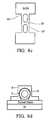
- FIG. 1 ashows a perspective view of an exemplary transistor 1 having a source 2 and drain 4 formed of a semiconductor nano-wire. Extending between the source and drain is a channel region 7 (as shown in cross sectional view FIG. 1 b ).
- a gate dielectric 10wraps around the channel region 7 and a gate electrode 8 wraps around the gate dielectric. Electric field effects that gate electrode 8 exerts on channel region 7 are schematically illustrated by arrows 12 in FIG. 1 b.
- the transistor channelmay be oriented vertically or horizontally.
- Many of the existing designs for horizontally oriented channelshave a square or rectangular shaped cross-section.
- the channel cross-sectionis rectangular or square, enhanced field effects at the corners of the rectangle may cause that part of the transistor to turn on earlier (i.e., having a lower threshold voltage) than parts of the transistor at the flat sides of the rectangular channel cross-section. This may result in a parasitic off-state leakage.
- a cylindrical channel cross-sectionis preferred over a rectangular channel cross-section.
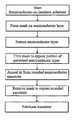
- the present inventionprovides for a method of manufacturing a semiconductor device.
- the methodincludes providing a semiconductor structure comprising a semiconductor layer overlying an insulating material and forming a patterned mask over said semiconductor layer.
- the methodfurther includes patterning the semiconductor layer to form a source region, a channel region, and a drain region in the semiconductor layer, wherein the channel region extends between the source region and the drain region.
- the channel region cornersare rounded by annealing, and the patterned mask is then removed.
- the methodmay further include forming a gate dielectric and a gate electrode about the rounded channel region.
- the methodmay further include trimming the patterned mask prior to the annealing step.
- the channel regionincludes two, closely spaced features that form a tube-like channel region when annealed.
- the inventionprovides for a semiconductor device having an insulating layer over an underlying layer.
- the devicealso has a layer of semiconductor material over the insulating layer, the semiconductor layer having a source region, a drain region, and a horizontal nano-wire structure extending between the source and drain regions.
- the nano-wire structureis in contact with said insulating layer.
- the deviceincludes a gate dielectric formed on the surface of at least a segment of the nano-wire structure and a gate electrode formed on the surface of the gate dielectric.
- the nano-wire structurehas a diameter of less than about 20 nm.
- the nano-wire structureis formed of two thin semiconductor features that fuse together to form a substantially hollow tube during an anneal step.
- the nano-wiremay have a cross section that is substantially circular, oval, elliptical, square, rectangular, or other shape.
- An advantageous feature of the present inventionis that the likelihood of necking (narrowing down) or breaking of the nano-wire is reduced or possibly eliminated.
- Another advantageous feature of the present inventionis that the agglomeration of silicon atoms in or near the source and drain regions is substantially reduced.
- FIG. 1 ashows in perspective an exemplary surround-gate or gate-all-around transistor employing a nano-wire channel region, which is also shown in cross sectional view in FIG. 1 b;
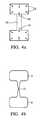
- FIG. 2 ashows a double-gate FinFET
- FIG. 2 bshows an Omega FinFET
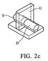
- FIG. 2 cshows a Nano-wire FinFET
- FIGS. 3 a through 3 fillustrate broken and narrowed nano-wires that may occur using a hydrogen annealing process
- FIGS. 4 a and 4 bschematically illustrate the migration of atoms of the active region during the anneal process, resulting in the formation of broken nano-wires;
- FIGS. 5 a and 5 bpreferred embodiment of this invention, in which the area available for silicon atoms to migrate is drastically reduced;
- FIG. 6shows a flow-chart illustrating the process flow of preferred embodiments of this invention to form a rounded nano-wire
- FIGS. 7 a through 7 hshow a series of device structures formed at the various steps of the process flow of FIG. 6 ;
- FIGS. 8 a through 8 dshow nano-tube formation according to another embodiment of this invention.
- Example embodiments of the present inventionwill be described herein in a specific context of making semiconductor devices, such as transistors. In other embodiments not shown, embodiments of the present invention also may include nano-wires or quantum-wires formed in accordance with the present invention. The present invention may also be applied, however, to other situations.
- FIGS. 2 a through 2 cshow the evolution of multiple-gate transistors or FinFETs.
- FinFETsare essentially field effect transistors with a fin-like or wire-like body region, as illustrated in FIG. 2 .
- the conventional double-gate FinFET deviceis taught in U.S. Pat. No. 6,413,802 B1 issued to Hu, et al.
- the double-gate transistorhas a gate electrode that straddles across the channel or the fin-like silicon body, thus forming a double-gate structure.
- omega-FinFETAs illustrated in FIG. 2 b.
- the Omega ( ⁇ ) field effect transistor (FET), or omega-FinFEThas a gate electrode that has an omega-shape in its cross-sectional view.
- the encroachment of the gate electrode under the semiconductor fin or bodyforms an omega-shaped gate structure. It closely resembles the Gate-All-Around (GAA) transistor for excellent scalability, and uses a very manufacturable process similar to that of the double-gate or triple-gate transistor.
- GAAGate-All-Around
- omega-FinFETDetails of the omega-FinFET are documented in Fu-Liang Yang, et al., “25 nm CMOS Omega-FETs,” IEEE International Electron Device Meeting, Technical Digest, pp. 255-258, San Francisco, Calif., Dec. 2002, which paper is incorporated herein by reference.
- a further improvement to the omega FinFETis the use of a nano-wire to form the body or channel of the FinFET.
- T Si requirementarises from the fact that when T Si is too large, short channel effects worsen, leading to high off-state leakage.
- a maximum T Siis specified and this maximum T Si is dependent on the device structure used. If T Si is too small, particularly when it is smaller than the minimum feature size or gate length L g , it becomes an unnecessarily restrictive requirement that is often undesirable from the perspective of manufacturability and device performance. For example, it is desired that the smallest feature size in a device is the gate length and not the silicon body width. As illustrated in FIG.
- the maximum T Si for adequate suppression of short-channel effectsis (2 ⁇ 3)L g . Requiring that the maximum T Si is smaller than L g is an undesirable attribute of the double-gate FinFET.
- An omega-FinFET[ FIG. 2 b ] relaxes the T Si requirement so that a maximum T Si of L g will be acceptable for effective control of short-channel effects.
- the nano-wire FinFET of the preferred embodiments of the present invention[ FIG. 2 c ] relaxes the requirement even further, requiring a maximum T Si of 2 L g .
- the nano-wire FinFET's relaxed requirement on T Sitherefore enlarges the device design space and may also enhance manufacturability.
- T Sithe maximum T Si required for nano-wire FinFETs is relaxed compared to double-gate or omega-FinFETs
- the value of T Si to be employed in sub-20 nm gate length nano-wire-FinFETis still about 40 nm or smaller. This is a very small dimension.
- a method of reliably controlling the diameter of nano-wiresis important. The formation of nano-wires with such small diameters is particularly challenging since nano-wires with such narrow diameters break easily.
- FIG. 3where the top view of silicon active regions observed using scanning electron microscopy (SEM) are illustrated.
- SEMscanning electron microscopy
- a silicon active region 14 which comprises a thin silicon line 16(which will in fact be the channel region in the preferred embodiment FinFET device) is annealed in a hydrogen ambient to form a nano-wire with a rounded cross-section.
- the annealing temperatureis typically 950 degrees Celsius, pressure is 10 Torr, and anneal time is 60 seconds.
- the rounding of corners of the source and/or drain regions 2 and 4 respectively,are also noticeable in addition to the formation of nano-wires with a rounded cross-section.
- the annealfacilitates silicon atom migration which contributes to the rounding effect.
- a direct result of the silicon migrationis the agglomeration of silicon in regions 3 and 5 in the large source or drain regions 2 and 4 , respectively, as indicated in FIG. 3 a.
- Excessive silicon migration from the thin silicon line 16 to agglomerate with other silicon atoms in the source 2 or drain 4 regionsleads to the breaking of the silicon line 16 at a point 17 , as shown in FIG. 3 a. While breaking point 17 is illustrated as being at or near the mid-point of silicon line 16 , this is not always or necessarily the case.
- Silicon line 16may neck down and/or break at other locations along its length.
- a silicon line 16 with a much larger widthsuch as that shown in FIG. 3 b, is not broken.
- Such a thick silicon lineis disadvantageous, however, since the resulting device would be a planar device. Unlike a multiple-gate transistor, a planar device formed from a thick silicon line would have limited scalability.
- FIG. 3 can active region with a different layout or perimeter is shown. Near breaking of silicon lines is also observed.
- FIG. 3 dshows a low magnification view of an array of nano-wire structures, illustrating that the problem of broken silicon lines is common in many neighboring layouts.
- FIG. 4conceptually illustrates the silicon migration and impact on the nano-wire.
- Annealing in hydrogen ambient at elevated temperaturesencourages silicon atom migration and forms nano-wires with round cross-sections.
- a re-distribution of silicon atoms within the nano-wireis sufficient to achieve the desired result.
- silicon atomsalso migrate from the nano-wire towards the source and drain region (as indicated by the bold arrows 18 ) during the hydrogen anneal process. It is the migration of silicon atoms away from the nano-wire that leads to a phenomenon of nano-wire necking. When there is extreme necking, such as that shown in FIG.
- the nano-wireis broken after the anneal.
- the migration of silicon atoms from the outer regions of source and drain regions 2 and 4 , respectively,is also illustrated in FIG. 4 a by the arrows 22 . This migration leads to corner rounding of the source and drain regions as well as during annealing, as also shown in FIG. 4 b.
- the preferred embodiments of the present inventionprovide for the insertion of a masked region on at least one of the source and drain regions.
- the mask 24comprises a material to which silicon atoms do not migrate, such as silicon nitride, silicon oxynitride, silicon oxide, or other dielectric. Since silicon atoms do not migrate to a region comprising the mask material, the amount or extent of silcon migration to the source and/or drain regions is limited.
- FIG. 5 ashows some silicon migration occurs (shown by the arrows 18 and 22 ), but the amount of silicon atom migration is significantly reduced by the inclusion of mask 24 .
- FIG. 5 bThe top view of the anneal silicon nano-wire is illustrated in FIG. 5 b. Note the schematically illustrated absence of necking of nano-wire 16 .
- FIG. 6shows an example of the process flow for forming a nano-wire without the abovementioned problem.
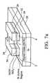
- Some of the manufacturing steps of this preferred embodiment being used to make a nano-wire FinFET embodimentare illustrated in FIGS. 7 a -( h ). While describing the structure formation steps shown in FIGS. 7 a -( h ), process parameters and steps for the preferred embodiment will be described, as well as some of the possible alternatives or variations of the process parameters and steps. However, the process parameters shown and/or described herein are merely examples to illustrate and describe the present invention. With the benefit of this disclosure, one of ordinary skill in the art will likely realize other variations and embodiments of the present invention within the scope and spirit of the appended patent claims.
- FIG. 7shows the three-dimensional perspective of one transistor device being manufactured in an integrated circuit (IC) chip using one embodiment of the process flow.
- ICintegrated circuit
- a semiconductor-on-insulator substratecomprising a semiconductor layer overlaying an insulator layer.
- the semiconductor layeris silicon
- this type of structureis sometimes referred to as a silicon-on-insulator substrate and is commonly available as a starting material.
- the semiconductor layermay be comprised of an alloy semiconductor such as silicon-germanium (SiGe), silicon-germanium-carbon (SiGeC), or silicon-carbon (SiC).
- the semiconductor layermay also comprise a binary III-V semiconductor such as gallium arsenide and indium antimonide or comprise a ternary III-V semiconductor such as gallium indium arsenide.
- the semiconductor layermay also comprise an elemental semiconductor such as silicon or germanium. Accordingly, a rounded semiconductor nano-wire may be formed from the semiconductor layer constituting the starting material.
- a mask 32is formed over the semiconductor layer.
- the maskcomprises a topmost silicon oxynitride layer 34 overlying a silicon oxide layer 36 ( FIG. 7 a ).
- the silicon oxide layer 36is also known as a pad oxide layer and may be thermally grown in a O 2 or H 2 O ambient at temperatures in the range of 600 degrees Celsius to 1100 degrees Celsius.
- the thickness of the silicon oxide layer 36is preferably between 10 angstroms and 300 angstroms, although thicknesses outside this range may also be used.
- the silicon oxynitride layer 34may be deposited by chemical vapor deposition at temperatures in the range of 300 degrees Celsius to 900 degrees Celsius.
- the thickness of the silicon oxynitride layer 34is preferably in the range of 100 angstroms to 4000 angstroms.
- the maskmay also be a single-layer mask, or a multi-layered mask.
- the maskis then patterned using photolithography.
- a photoresist (not shown) used in the photolithography processmay or may not be removed at this step.
- the mask 32is then used to etch the underlying semiconductor layer 26 .
- An anisotropic etch or a dry plasma etchis preferably employed.
- the semiconductor layeris silicon
- the insulator layer 30is a buried silicon oxide. After the etching of the semiconductor layer, an active region is formed.
- the process step illustrated in FIG. 7 ais also known as active region definition.
- the patterned semiconductor layer or active regionremains in the form of an H-shaped, thin silicon island 26 .
- the patterned semiconductor layermay have other shapes (e.g., U-shaped, V-shaped, I-shaped, L-shaped, etc.).
- the thickness of the patterned silicon layer or islandmay range from about two angstroms to about 1000 angstroms, for example.
- the patterned silicon layerhas a source region 2 , a drain region 4 , and a channel region 7 .
- the channel region 7extends between the source region and the drain region. As shown in FIG. 7 a, the channel region has a width that is much narrower than the contact pad portions and of the source and drain regions.
- the underlying layer 28 beneath the insulator or buried silicon oxide (BOX) 30 layerwill often be a silicon wafer, for example.
- the underlying layermay be comprised of another type of material, including but not limited to: an elemental semiconductor, such as germanium; an alloy semiconductor, such as silicon-germanium; or a compound semiconductor, such as gallium arsenide or indium phosphide, for example.
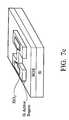
- the patterned maskis trimmed such that it recedes from the edge of the active region, as shown in FIG. 7 b.
- the amount of trim or the distance by which the patterned mask recedes from the edge of the active regionis preferably in the range of 20 angstroms to 5000 angstroms.
- the trimmingcan be performed by using a wet etch or a dry plasma etch process. According to this invention, the patterned mask is not completely removed at this step.
- the topmost layer of the maskmay be optionally removed.
- the topmost silicon oxynitride layer of the mask in the preferred embodimentmay be removed to give the structure as shown in FIG. 7 c. This can be performed by using a wet etch in hot (approximately 150 to 170 degrees Celsius) phosphoric acid.
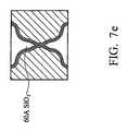
- the silicon atoms in the patterned silicon layerare re-arranged by annealing the silicon layer at elevated temperatures [ FIG. 7 d ].
- the re-arrangementis induced by surface migration of silicon atoms driven by a tendency to minimize surface tension.
- the re-arrangement of the atoms at the narrow channel regioncauses the corners of the channel region to be rounded to transform the channel region into a nano-wire structure. If carried out long enough and/or under sufficient heat, the resulting nano-wire structure may be completely rounded having a circular-shaped cross-section.
- the contact pad portions of the source and drain regionswill also likely experience slight shape changes, such as rounding of at least some of their corners.
- the contact pad portions of the source and drain regionsserve to provide a portion onto which metallic or conductive materials form electrical connection with the source and drain regions. It is understood that the contact pad is an optional feature of this invention. If the contact pad portions of the source and drain regions are omitted, the patterned semiconductor layer may be I-shaped, for example. In this case, the electrical connection between the metallic or conductive material and the source and drain regions may be formed directly on the nano-wire structure.
- the temperature for the annealing processmay range from about 600 degrees Celsius to about 1200 degrees Celsius.
- the anneal timemay range from about one second to about two hours.
- the pressure in the reaction chamber (not shown) used for the annealing processmay vary, depending in part upon the environment within the reaction chamber.
- the reaction chambermay be a chemical vapor deposition (CVD) epitaxial reactor, for example.
- the annealing processmay occur in a reaction chamber having an environment of hydrogen gas (H 2 ) at a partial pressure ranging from about 1.0 ⁇ 10 ⁇ 9 torr to about 800 torr.
- the annealing environmentmay be evacuated (i.e., a vacuum environment) at a pressure ranging from about 1.0 ⁇ 10 ⁇ 10 torr to about 1.0 ⁇ 10 ⁇ 3 torr.
- the annealing environmentmay be nitrogen gas (N 2 ) at a pressure ranging from about 1.0 ⁇ 10 ⁇ 9 torr to about 800 torr.
- the annealing environmentmay also be one of the following environments (but not limited to): an environment of a mixed gas including hydrogen and argon; an environment of a mixed gas including hydrogen and nitrogen; an environment with other gases in addition to hydrogen to form a mixed gas ambient; or an environment of an inert gas, for example.
- the annealing processis performed in a hydrogen gas (H 2 ) ambient at about 900-950 degrees Celsius for about 1 minute.
- H 2hydrogen gas
- An example of the annealed structureis shown in FIG. 7 e.
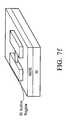
- the mask layer or remaining portion of the mask layermay be completely removed at this step.
- the pad oxide layeris removed, as shown in FIG. 7 f. Removal of the pad oxide layer is preferably done using a wet etch in dilute hydrofluoric acid (HF).
- HFdilute hydrofluoric acid
- a single masking layeris used to both define the active area island 26 and also to mask the source and/or drain regions during the anneal process.
- two different masking layerscould be employed. One masking layer could be employed for defining and patterning the active area island, which mask may be removed, followed by definition of a second, separate mask to define the masked regions for the annealing step. While this embodiment would eliminate the need to trim the mask, as described above, it would involve additional masking definition steps and would not provide the advantage of being self-aligned.
- a gate stackcomprises a gate dielectric and a gate electrode.
- a gate dielectric materialis formed on the surface of and about the nano-wire structure (as well as on the other exposed portions of the silicon layer).
- the gate dielectric materialmay be an oxide formed by thermal oxidation or atomic-layer CVD for uniform deposition, for example. Hence, the gate dielectric will likely form on all exposed areas, including the contact portions of the source and drain regions.
- the gate dielectric materialmay take the form of a variety of compositions, including but not limited to: silicon dioxide (SiO 2 ), silicon oxynitride (SiO x N y ), HfO 2 , ZrO 2 , Al 2 O 3 , La 2 O 3 , or other high permittivity materials, for example.
- a gate electrode material 40is then deposited, masked, and etched to form the gate electrode, as shown in FIG. 7 g.
- the gate electrode materialmay be selected from a variety of materials, including but not limited to: a semiconductor material (e.g., poly-silicon, poly-silicon-germanium); a metal material (e.g., molybdenum, tungsten, titanium); a metallic nitride (e.g., tantalum nitride, titanium nitride); or any combination thereof, for example.
- the gate dielectric materialmay be removed from the source and drain regions.
- the gate dielectricis preferably aligned with the gate electrode at the channel, the gate dielectric can be self-aligned with the gate electrode by simply etching the gate electrode material with an etch chemistry that will also etch away the gate dielectric material while being selective against etching the silicon layer. Also, because the gate dielectric at the gate channel is shielded by the gate electrode, the ion implantation processes for doping the silicon layer outside of the channel (i.e., to form the source and drain of the transistor) may be self-aligning as well.
- the nano-wire 16has a diameter no larger than about 30 nm, and even more preferably no larger than 20 nm.
- the diameter of the nano-wire cross-sectionmay be in the order of nanometers (e.g., about 4 nm), and such nano-wires may be used for the channel of a field effect transistor, for example.
- a nanotube instead of a nano-wiremay be formed by placing two semiconductor fins or lines 16 ′, 16 ′′ in close proximity to each other prior to anneal.
- the separation between the two semiconductor lines 16 ′, 16 ′′may be less than 10 nm apart, as shown FIG. 8 a.
- a three-dimensional perspective of the structureis depicted in FIG. 8 b.
- the two semiconductor linesmay be connected at selected portions 36 , such as shown in FIG. 8 c.
- a semiconductor nanotubemay be formed with a hollow core 7 ′.
- Gate dielectric 10 and gate electrode 8may then be formed to complete a semiconductor nanotube transistor device. A cross-section of the device is shown in FIG. 8 d. Semiconductor materials previously described for the nano-wire FinFET may be used for the semiconductor nanotube.
Landscapes
- Engineering & Computer Science (AREA)
- Chemical & Material Sciences (AREA)
- Physics & Mathematics (AREA)
- Nanotechnology (AREA)
- General Physics & Mathematics (AREA)
- Crystallography & Structural Chemistry (AREA)
- Theoretical Computer Science (AREA)
- Condensed Matter Physics & Semiconductors (AREA)
- Mathematical Physics (AREA)
- Manufacturing & Machinery (AREA)
- Computer Hardware Design (AREA)
- Microelectronics & Electronic Packaging (AREA)
- Power Engineering (AREA)
- Thin Film Transistor (AREA)
- Insulated Gate Type Field-Effect Transistor (AREA)
- Bipolar Transistors (AREA)
Abstract
Description
- This application claims priority to provisional patent application Ser. No. 60/578,673 filed on Jun. 10, 2004, entitled “Semiconductor Nanowire Devices and Methods of Fabrication,” which application is hereby incorporated herein by reference.
- The present invention relates generally to methods for manufacturing semiconductor devices. In particular, this invention teaches a method of forming a nano-wire structure for a channel of a field effect transistor.
- Metal-oxide-semiconductor field effect transistors (MOSFETs) are used in ultra-large scale integrated (ULSI) circuits, which are found in today's semiconductor integrated circuit (IC) chip products. The gate length of the MOSFET is continuously being scaled down for faster circuit speed, higher circuit density and increased functionality, and lower cost per unit function. As the gate length of the MOSFET is scaled into the sub-20 nm regime, the source and drain increasingly interact with the channel to substantially influence the channel potential. Hence, a transistor with a short gate length often suffers from problems related to the inability of the gate to substantially control the on/off states of the channel. Phenomena related to the reduced gate control of the channel potential are called short-channel effects.
- Increased body doping concentration, reduced gate oxide thickness, and junction depths are some ways to suppress short-channel effects. However, for device scaling well into the sub-20 nm regime, the requirements for body-doping concentration, gate oxide thickness, and source/drain doping profiles become increasingly difficult to meet using conventional device structures based on bulk silicon substrates. Therefore, alternative device structures that offer better control of short-channel effects are being considered to enable the continued scaling down of transistor sizes.
- A highly scalable device structure that offers superior control of short-channel effects is a wrap-around gate structure for a transistor (a.k.a., surround-gate or gate-all-around transistor structure). A wrap-around gate structure typically has a gate that surrounds or wraps around a channel region. This structure effectively improves the capacitance coupling between the gate and the channel, as compared to conventional bulk silicon substrate transistor structures, double-gate transistor structures, and triple-gate transistor structures. With the wrap-around gate structure, the gate gains significant influence on the channel potential, and therefore improves suppression of short-channel effects. A wrap-around gate structure typically allows the gate length to be scaled down by about 50% more compared to a double-gate structure. An example of a wrap-around gate structure is illustrated in
FIG. 1 . More specifically,FIG. 1 ashows a perspective view of anexemplary transistor 1 having asource 2 anddrain 4 formed of a semiconductor nano-wire. Extending between the source and drain is a channel region7 (as shown in cross sectional viewFIG. 1 b). A gate dielectric10 wraps around thechannel region 7 and agate electrode 8 wraps around the gate dielectric. Electric field effects thatgate electrode 8 exerts onchannel region 7 are schematically illustrated byarrows 12 inFIG. 1 b. - There are several different ways to implement a wrap-around gate transistor structure. For example, the transistor channel may be oriented vertically or horizontally. Many of the existing designs for horizontally oriented channels have a square or rectangular shaped cross-section. When the channel cross-section is rectangular or square, enhanced field effects at the corners of the rectangle may cause that part of the transistor to turn on earlier (i.e., having a lower threshold voltage) than parts of the transistor at the flat sides of the rectangular channel cross-section. This may result in a parasitic off-state leakage. Hence, a cylindrical channel cross-section is preferred over a rectangular channel cross-section.
- Current attempts at obtaining a more circular channel cross-section are made by oxidizing the silicon beam forming the channel to round the corners of the rectangular channel cross-section. However, this method requires a large amount of oxidation, and hence a large amount of oxide formation, to convert the rectangular channel cross-section shape to a rounded or circular channel cross-section. Hence, there is a need for a way to manufacture a transistor channel, preferably having a rounded or circular cross-section shape, without having to form excessive oxide about the channel.
- In one aspect, the present invention provides for a method of manufacturing a semiconductor device. The method includes providing a semiconductor structure comprising a semiconductor layer overlying an insulating material and forming a patterned mask over said semiconductor layer. The method further includes patterning the semiconductor layer to form a source region, a channel region, and a drain region in the semiconductor layer, wherein the channel region extends between the source region and the drain region. The channel region corners are rounded by annealing, and the patterned mask is then removed. In some embodiments, the method may further include forming a gate dielectric and a gate electrode about the rounded channel region. In some embodiments, the method may further include trimming the patterned mask prior to the annealing step. In yet other embodiments, the channel region includes two, closely spaced features that form a tube-like channel region when annealed.
- In another aspect, the invention provides for a semiconductor device having an insulating layer over an underlying layer. The device also has a layer of semiconductor material over the insulating layer, the semiconductor layer having a source region, a drain region, and a horizontal nano-wire structure extending between the source and drain regions. The nano-wire structure is in contact with said insulating layer. The device includes a gate dielectric formed on the surface of at least a segment of the nano-wire structure and a gate electrode formed on the surface of the gate dielectric. In some embodiments, the nano-wire structure has a diameter of less than about 20 nm. In other embodiments, the nano-wire structure is formed of two thin semiconductor features that fuse together to form a substantially hollow tube during an anneal step. The nano-wire may have a cross section that is substantially circular, oval, elliptical, square, rectangular, or other shape.
- An advantageous feature of the present invention is that the likelihood of necking (narrowing down) or breaking of the nano-wire is reduced or possibly eliminated. Another advantageous feature of the present invention is that the agglomeration of silicon atoms in or near the source and drain regions is substantially reduced.
- For a more complete understanding of the present invention, and the advantages thereof, reference is now made to the following descriptions taken in conjunction with the accompanying drawings, in which:
FIG. 1 ashows in perspective an exemplary surround-gate or gate-all-around transistor employing a nano-wire channel region, which is also shown in cross sectional view inFIG. 1 b;FIG. 2 ashows a double-gate FinFET,FIG. 2 bshows an Omega FinFET, andFIG. 2 cshows a Nano-wire FinFET;FIGS. 3 athrough3fillustrate broken and narrowed nano-wires that may occur using a hydrogen annealing process;FIGS. 4 aand4bschematically illustrate the migration of atoms of the active region during the anneal process, resulting in the formation of broken nano-wires;FIGS. 5 aand5bpreferred embodiment of this invention, in which the area available for silicon atoms to migrate is drastically reduced;FIG. 6 shows a flow-chart illustrating the process flow of preferred embodiments of this invention to form a rounded nano-wire;FIGS. 7 athrough7hshow a series of device structures formed at the various steps of the process flow ofFIG. 6 ; andFIGS. 8 athrough8dshow nano-tube formation according to another embodiment of this invention.- The use of presently preferred embodiments is discussed in detail below. It should be appreciated, however, that the present invention provides many applicable inventive concepts that can be embodied in a wide variety of specific contexts. The specific embodiments discussed are merely illustrative of specific ways to make and use the invention, and do not limit the scope of the invention.
- Example embodiments of the present invention will be described herein in a specific context of making semiconductor devices, such as transistors. In other embodiments not shown, embodiments of the present invention also may include nano-wires or quantum-wires formed in accordance with the present invention. The present invention may also be applied, however, to other situations.
FIGS. 2 athrough2cshow the evolution of multiple-gate transistors or FinFETs. FinFETs are essentially field effect transistors with a fin-like or wire-like body region, as illustrated inFIG. 2 . The conventional double-gate FinFET device is taught in U.S. Pat. No. 6,413,802 B1 issued to Hu, et al. As illustrated inFIG. 2 a,the double-gate transistor has a gate electrode that straddles across the channel or the fin-like silicon body, thus forming a double-gate structure. There are two gates, one on each sidewall of the silicon fin, as shown inFIG. 2 a.- Improvements to the double-gate FinFET has led to omega-FinFET, as illustrated in
FIG. 2 b.The Omega (Ω) field effect transistor (FET), or omega-FinFET has a gate electrode that has an omega-shape in its cross-sectional view. The encroachment of the gate electrode under the semiconductor fin or body forms an omega-shaped gate structure. It closely resembles the Gate-All-Around (GAA) transistor for excellent scalability, and uses a very manufacturable process similar to that of the double-gate or triple-gate transistor. Details of the omega-FinFET are documented in Fu-Liang Yang, et al., “25 nm CMOS Omega-FETs,”IEEE International Electron Device Meeting, Technical Digest,pp. 255-258, San Francisco, Calif., Dec. 2002, which paper is incorporated herein by reference. - Earlier versions of FinFET have sharp edges or corners on the semiconductor fin or channel region. Regions near the sharp corners, where the radius of curvature is relatively small, turn on or form an inversion layer at a lower gate voltage, and therefore potentially contribute to a high off-state leakage current between the source and the drain. The high local electric field at sharp corners also negatively impacts the gate dielectric integrity. Therefore, a further improvement to the omega FinFET, according to one embodiment of this invention, is the use of a nano-wire to form the body or channel of the FinFET.
- Yet another advantage of using the nano-wire-FinFET structure of this invention is the relaxation of the silicon body width TSirequirement. The TSirequirement arises from the fact that when TSiis too large, short channel effects worsen, leading to high off-state leakage. To achieve adequate suppression of short-channel effects, a maximum TSiis specified and this maximum TSiis dependent on the device structure used. If TSiis too small, particularly when it is smaller than the minimum feature size or gate length Lg, it becomes an unnecessarily restrictive requirement that is often undesirable from the perspective of manufacturability and device performance. For example, it is desired that the smallest feature size in a device is the gate length and not the silicon body width. As illustrated in
FIG. 2 a,for the double-gate FinFET structure, it can be empirically determined that the maximum TSifor adequate suppression of short-channel effects is (⅔)Lg. Requiring that the maximum TSiis smaller than Lgis an undesirable attribute of the double-gate FinFET. An omega-FinFET [FIG. 2 b] relaxes the TSirequirement so that a maximum TSiof Lgwill be acceptable for effective control of short-channel effects. The nano-wire FinFET of the preferred embodiments of the present invention [FIG. 2 c] relaxes the requirement even further, requiring a maximum TSiof2Lg. The nano-wire FinFET's relaxed requirement on TSitherefore enlarges the device design space and may also enhance manufacturability. - Despite the fact that the maximum TSirequired for nano-wire FinFETs is relaxed compared to double-gate or omega-FinFETs, the value of TSito be employed in sub-20 nm gate length nano-wire-FinFET is still about 40 nm or smaller. This is a very small dimension. In order to form nano-wires suitable for the fabrication of nano-wire-FinFET devices with sub-20 nm gate lengths, a method of reliably controlling the diameter of nano-wires is important. The formation of nano-wires with such small diameters is particularly challenging since nano-wires with such narrow diameters break easily.
- Further information relating to preferred methods and structures for FinFET devices, while relevant but not necessary for an understanding of the present invention, may be found in the following co-pending and commonly owned U.S. patent applications, each of which is incorporated herein by reference: Ser. No. 10/314,249, filed Oct. 6, 2002, entitled “Multiple-Gate Transistor and Methods of Manufacture,” (Attorney Docket Number TSMC2002-0856); Ser. No. 10/305,841, filed Nov. 26, 2002, entitled “Strained-Channel Multiple-Gate Transistor,” (Attorney Docket Number TSMC2002-0895); Ser. No. 10/370,792, filed Feb. 20, 2003, entitled “Semiconductor Nano-Rod Devices,” (Attorney Docket Number TSMC2002-0896); Ser. No. 10/319,119, filed Dec. 12, 2002, entitled “Semiconductor-On Insulator Chip Incorporating Partially-Depleted, Fully-Depleted, and Multiple-Gate Devices,” (Attorney Docket Number TSMC2002-0979); Ser. No. 10/401,087, filed Mar. 26, 2003, entitled “Semiconductor-On-Insulator Chip Incorporating Partially-Depleted, Fully-Depleted, and Multiple-Gate Devices,” (Attorney Docket Number TSMC2002-1059); Ser. No. 10/313,887, Dec. 6, 2002, entitled “CMOS Inverters Configured Using Multiple-Gate Transistors,” (Attorney Docket Number TSMC2002-1080); Ser. No. 10/305,728, filed Nov. 26, 2002, entitled “CMOS SRAM Cell Configured Using Multiple-Gate Transistors,” (Attorney Docket Number TSMC2002-1116); Ser. No. 10/377,479, filed Feb. 27, 2003, entitled “Contacts to Semiconductor FIN Devices,” (Attorney Docket Number TSMC2002-1199); Ser. No. 10/425,156, filed Apr. 29, 2003, entitled “Doping of Semiconductor Fin Devices,” (Attorney Docket Number TSMC2003-0175); Ser. No. 10/608,287, filed Jun. 27, 2003, entitled “Structure and Method for Forming the Gate Electrode in a Multiple-Gate Transistor,” (Attorney Docket Number TSMC2003-0421).
- Our previous invention, Ser. No. 10/370,792, filed Feb. 20, 2003, entitled “Semiconductor Nano-Rod Devices,” (Attorney Docket Number TSMC2002-0896) detailed a particular method of forming a nano-wire or nano-rod field effect transistor. Experimental results indicate that the method taught in that prior application is adequate for forming nano-wires with diameters larger than about 20 nm.
- For nano-wires with diameters smaller than 20 nm, serious problems related to the breaking of nano-wires during hydrogen anneal may occur. Such problems are illustrated in
FIG. 3 , where the top view of silicon active regions observed using scanning electron microscopy (SEM) are illustrated. InFIG. 3 a,a silicon active region14 which comprises a thin silicon line16 (which will in fact be the channel region in the preferred embodiment FinFET device) is annealed in a hydrogen ambient to form a nano-wire with a rounded cross-section. The annealing temperature is typically 950 degrees Celsius, pressure is 10 Torr, and anneal time is 60 seconds. The rounding of corners of the source and/ordrain regions regions drain regions FIG. 3 a.Excessive silicon migration from thethin silicon line 16 to agglomerate with other silicon atoms in thesource 2 or drain4 regions leads to the breaking of thesilicon line 16 at apoint 17, as shown inFIG. 3 a.Whilebreaking point 17 is illustrated as being at or near the mid-point ofsilicon line 16, this is not always or necessarily the case.Silicon line 16 may neck down and/or break at other locations along its length. By contrast, asilicon line 16 with a much larger width, such as that shown inFIG. 3 b,is not broken. Such a thick silicon line is disadvantageous, however, since the resulting device would be a planar device. Unlike a multiple-gate transistor, a planar device formed from a thick silicon line would have limited scalability. InFIG. 3 c,an active region with a different layout or perimeter is shown. Near breaking of silicon lines is also observed. - The observation of broken or nearly broken silicon lines or silicon nano-wires upon annealing in hydrogen ambient is also noted for layouts where there are multiple silicon lines connecting between the source and drain regions. This is shown in
FIG. 3 dwhere the silicon lines are broken or almost broken. InFIG. 3 e,where there are 3 parallel silicon lines, one silicon line located in the middle is broken.FIG. 3 fshows a low magnification view of an array of nano-wire structures, illustrating that the problem of broken silicon lines is common in many neighboring layouts. FIG. 4 conceptually illustrates the silicon migration and impact on the nano-wire. Annealing in hydrogen ambient at elevated temperatures encourages silicon atom migration and forms nano-wires with round cross-sections. To form a nano-wire 16 with a substantially round cross-section, a re-distribution of silicon atoms within the nano-wire is sufficient to achieve the desired result. However, in reality, as shown inFIG. 4 a,silicon atoms also migrate from the nano-wire towards the source and drain region (as indicated by the bold arrows18) during the hydrogen anneal process. It is the migration of silicon atoms away from the nano-wire that leads to a phenomenon of nano-wire necking. When there is extreme necking, such as that shown inFIG. 4 b,the nano-wire is broken after the anneal. The migration of silicon atoms from the outer regions of source anddrain regions FIG. 4 aby thearrows 22. This migration leads to corner rounding of the source and drain regions as well as during annealing, as also shown inFIG. 4 b.- To avoid the problems of too much silicon atom migration from the silicon nano-wire to the source and drain regions, the preferred embodiments of the present invention provide for the insertion of a masked region on at least one of the source and drain regions. This is schematically illustrated in
FIG. 5 a.Themask 24 comprises a material to which silicon atoms do not migrate, such as silicon nitride, silicon oxynitride, silicon oxide, or other dielectric. Since silicon atoms do not migrate to a region comprising the mask material, the amount or extent of silcon migration to the source and/or drain regions is limited.FIG. 5 ashows some silicon migration occurs (shown by thearrows 18 and22), but the amount of silicon atom migration is significantly reduced by the inclusion ofmask 24. - By restricting silicon atom migration from the nano-wire to the source and/or drain regions, the necking problem is resolved or the likelihood of forming a broken silicon nano-wire is reduced. The top view of the anneal silicon nano-wire is illustrated in
FIG. 5 b.Note the schematically illustrated absence of necking of nano-wire 16. FIG. 6 shows an example of the process flow for forming a nano-wire without the abovementioned problem. Some of the manufacturing steps of this preferred embodiment being used to make a nano-wire FinFET embodiment are illustrated inFIGS. 7 a-(h). While describing the structure formation steps shown inFIGS. 7 a-(h), process parameters and steps for the preferred embodiment will be described, as well as some of the possible alternatives or variations of the process parameters and steps. However, the process parameters shown and/or described herein are merely examples to illustrate and describe the present invention. With the benefit of this disclosure, one of ordinary skill in the art will likely realize other variations and embodiments of the present invention within the scope and spirit of the appended patent claims.FIG. 7 shows the three-dimensional perspective of one transistor device being manufactured in an integrated circuit (IC) chip using one embodiment of the process flow. Such an IC chip will often have millions or perhaps billions of these transistors. However, for purposes of illustration and discussion, only one transistor device is shown.- First, a semiconductor-on-insulator substrate comprising a semiconductor layer overlaying an insulator layer is provided. When the semiconductor layer is silicon, this type of structure is sometimes referred to as a silicon-on-insulator substrate and is commonly available as a starting material. It should be noted that in this invention, the semiconductor layer may be comprised of an alloy semiconductor such as silicon-germanium (SiGe), silicon-germanium-carbon (SiGeC), or silicon-carbon (SiC). The semiconductor layer may also comprise a binary III-V semiconductor such as gallium arsenide and indium antimonide or comprise a ternary III-V semiconductor such as gallium indium arsenide. The semiconductor layer may also comprise an elemental semiconductor such as silicon or germanium. Accordingly, a rounded semiconductor nano-wire may be formed from the semiconductor layer constituting the starting material.
- A
mask 32 is formed over the semiconductor layer. In the preferred embodiment, the mask comprises a topmostsilicon oxynitride layer 34 overlying a silicon oxide layer36 (FIG. 7 a). Thesilicon oxide layer 36 is also known as a pad oxide layer and may be thermally grown in a O2or H2O ambient at temperatures in the range of 600 degrees Celsius to 1100 degrees Celsius. The thickness of thesilicon oxide layer 36 is preferably between 10 angstroms and 300 angstroms, although thicknesses outside this range may also be used. Thesilicon oxynitride layer 34 may be deposited by chemical vapor deposition at temperatures in the range of 300 degrees Celsius to 900 degrees Celsius. The thickness of thesilicon oxynitride layer 34 is preferably in the range of 100 angstroms to 4000 angstroms. In general, the mask may also be a single-layer mask, or a multi-layered mask. The mask is then patterned using photolithography. A photoresist (not shown) used in the photolithography process may or may not be removed at this step. Themask 32 is then used to etch theunderlying semiconductor layer 26. An anisotropic etch or a dry plasma etch is preferably employed. For example, inFIG. 7 a,the semiconductor layer is silicon, and theinsulator layer 30 is a buried silicon oxide. After the etching of the semiconductor layer, an active region is formed. The process step illustrated inFIG. 7 ais also known as active region definition. - In
FIG. 7 a,the patterned semiconductor layer or active region remains in the form of an H-shaped,thin silicon island 26. However, in other embodiments (not shown), the patterned semiconductor layer may have other shapes (e.g., U-shaped, V-shaped, I-shaped, L-shaped, etc.). The thickness of the patterned silicon layer or island may range from about two angstroms to about 1000 angstroms, for example. The patterned silicon layer has asource region 2, adrain region 4, and achannel region 7. Thechannel region 7 extends between the source region and the drain region. As shown inFIG. 7 a,the channel region has a width that is much narrower than the contact pad portions and of the source and drain regions. - The
underlying layer 28 beneath the insulator or buried silicon oxide (BOX)30 layer will often be a silicon wafer, for example. However, the underlying layer may be comprised of another type of material, including but not limited to: an elemental semiconductor, such as germanium; an alloy semiconductor, such as silicon-germanium; or a compound semiconductor, such as gallium arsenide or indium phosphide, for example. - Next, the patterned mask is trimmed such that it recedes from the edge of the active region, as shown in
FIG. 7 b.The amount of trim or the distance by which the patterned mask recedes from the edge of the active region is preferably in the range of 20 angstroms to 5000 angstroms. The trimming can be performed by using a wet etch or a dry plasma etch process. According to this invention, the patterned mask is not completely removed at this step. - The topmost layer of the mask, if it is a multi-layer mask, may be optionally removed. For example, the topmost silicon oxynitride layer of the mask in the preferred embodiment, may be removed to give the structure as shown in
FIG. 7 c.This can be performed by using a wet etch in hot (approximately 150 to 170 degrees Celsius) phosphoric acid. - Next, the silicon atoms in the patterned silicon layer are re-arranged by annealing the silicon layer at elevated temperatures [
FIG. 7 d]. The re-arrangement is induced by surface migration of silicon atoms driven by a tendency to minimize surface tension. During the annealing, the re-arrangement of the atoms at the narrow channel region causes the corners of the channel region to be rounded to transform the channel region into a nano-wire structure. If carried out long enough and/or under sufficient heat, the resulting nano-wire structure may be completely rounded having a circular-shaped cross-section. The contact pad portions of the source and drain regions will also likely experience slight shape changes, such as rounding of at least some of their corners. The contact pad portions of the source and drain regions serve to provide a portion onto which metallic or conductive materials form electrical connection with the source and drain regions. It is understood that the contact pad is an optional feature of this invention. If the contact pad portions of the source and drain regions are omitted, the patterned semiconductor layer may be I-shaped, for example. In this case, the electrical connection between the metallic or conductive material and the source and drain regions may be formed directly on the nano-wire structure. - Example parameters for the annealing process used to round the corners of the channel region will be described next. The temperature for the annealing process may range from about 600 degrees Celsius to about 1200 degrees Celsius. The anneal time may range from about one second to about two hours. The pressure in the reaction chamber (not shown) used for the annealing process may vary, depending in part upon the environment within the reaction chamber. The reaction chamber may be a chemical vapor deposition (CVD) epitaxial reactor, for example. The annealing process may occur in a reaction chamber having an environment of hydrogen gas (H2) at a partial pressure ranging from about 1.0×10⁻⁹torr to about 800 torr. In another embodiment, the annealing environment may be evacuated (i.e., a vacuum environment) at a pressure ranging from about 1.0×10⁻¹⁰torr to about 1.0×10⁻³torr. In still another embodiment, the annealing environment may be nitrogen gas (N2) at a pressure ranging from about 1.0×10⁻⁹torr to about 800 torr. The annealing environment may also be one of the following environments (but not limited to): an environment of a mixed gas including hydrogen and argon; an environment of a mixed gas including hydrogen and nitrogen; an environment with other gases in addition to hydrogen to form a mixed gas ambient; or an environment of an inert gas, for example.
- In a preferred embodiment, the annealing process is performed in a hydrogen gas (H2) ambient at about 900-950 degrees Celsius for about 1 minute. An example of the annealed structure is shown in
FIG. 7 e. - The mask layer or remaining portion of the mask layer may be completely removed at this step. In the preferred embodiment, the pad oxide layer is removed, as shown in
FIG. 7 f.Removal of the pad oxide layer is preferably done using a wet etch in dilute hydrofluoric acid (HF). In the above described embodiment, a single masking layer is used to both define theactive area island 26 and also to mask the source and/or drain regions during the anneal process. In an alternative embodiment, two different masking layers could be employed. One masking layer could be employed for defining and patterning the active area island, which mask may be removed, followed by definition of a second, separate mask to define the masked regions for the annealing step. While this embodiment would eliminate the need to trim the mask, as described above, it would involve additional masking definition steps and would not provide the advantage of being self-aligned. - This is followed by gate stack definition. A gate stack comprises a gate dielectric and a gate electrode. A gate dielectric material is formed on the surface of and about the nano-wire structure (as well as on the other exposed portions of the silicon layer). The gate dielectric material may be an oxide formed by thermal oxidation or atomic-layer CVD for uniform deposition, for example. Hence, the gate dielectric will likely form on all exposed areas, including the contact portions of the source and drain regions. The gate dielectric material may take the form of a variety of compositions, including but not limited to: silicon dioxide (SiO2), silicon oxynitride (SiOxNy), HfO2, ZrO2, Al2O3, La2O3, or other high permittivity materials, for example.
- A
gate electrode material 40 is then deposited, masked, and etched to form the gate electrode, as shown inFIG. 7 g.The gate electrode material may be selected from a variety of materials, including but not limited to: a semiconductor material (e.g., poly-silicon, poly-silicon-germanium); a metal material (e.g., molybdenum, tungsten, titanium); a metallic nitride (e.g., tantalum nitride, titanium nitride); or any combination thereof, for example. During or after the etching of the gate electrode material to form the patterned gate electrode, the gate dielectric material may be removed from the source and drain regions. - Because the gate dielectric is preferably aligned with the gate electrode at the channel, the gate dielectric can be self-aligned with the gate electrode by simply etching the gate electrode material with an etch chemistry that will also etch away the gate dielectric material while being selective against etching the silicon layer. Also, because the gate dielectric at the gate channel is shielded by the gate electrode, the ion implantation processes for doping the silicon layer outside of the channel (i.e., to form the source and drain of the transistor) may be self-aligning as well.
- Preferably, the nano-
wire 16 has a diameter no larger than about 30 nm, and even more preferably no larger than 20 nm. The diameter of the nano-wire cross-section may be in the order of nanometers (e.g., about 4 nm), and such nano-wires may be used for the channel of a field effect transistor, for example. - Referring now to
FIG. 8 , a second embodiment of this invention is described as follows. A nanotube instead of a nano-wire may be formed by placing two semiconductor fins orlines 16′,16″ in close proximity to each other prior to anneal. The separation between the twosemiconductor lines 16′,16″ may be less than 10 nm apart, as shownFIG. 8 a.A three-dimensional perspective of the structure is depicted inFIG. 8 b.The two semiconductor lines may be connected at selectedportions 36, such as shown inFIG. 8 c.After annealing, a semiconductor nanotube may be formed with ahollow core 7′. While the mechanism for such formation is not fully appreciated, it is speculated that annealing can lead to migration of silicon atoms to form the tube structure. This is not always, or even necessarily the case, however, and the teachings of the present invention are applicable even if the resulting structure does not form an actual tube or only forms an imperfect tube.Gate dielectric 10 andgate electrode 8 may then be formed to complete a semiconductor nanotube transistor device. A cross-section of the device is shown inFIG. 8 d.Semiconductor materials previously described for the nano-wire FinFET may be used for the semiconductor nanotube. - Although several embodiments of the present invention have been described in detail, it should be understood that various changes, substitutions and alterations can be made herein without departing from the spirit and scope of the invention as defined by the appended claims. Moreover, the scope of the present application is not intended to be limited to the particular embodiments of the processes, machines, manufactures, compositions of matter, means, methods and steps described in the specification. As one of ordinary skill in the art will readily appreciate from the disclosure of the present invention, processes, machines, manufactures, compositions of matter, means, methods, or steps, presently existing or later to be developed, that perform substantially the same function and/or achieve substantially the same result as the corresponding embodiments described herein may be utilized according to the present invention. Accordingly, the appended claims are intended to include within their scope such processes, machines, manufactures, compositions of matter, means, methods, or steps.
Claims (27)
1. A method of manufacturing a semiconductor device, comprising the steps of:
providing a semiconductor structure comprising a semiconductor layer overlying an insulating material;
forming a patterned mask over said semiconductor layer;
patterning the semiconductor layer to form a source region, a channel region, and a drain region in the semiconductor layer, wherein the channel region extends between the source region and the drain region;
rounding corners of the channel region by annealing; and
removing said patterned mask after said rounding step.
2. The method ofclaim 1 , further comprising a step, after the step of patterning the semiconductor layer, of trimming the patterned mask.
3. The method ofclaim 2 wherein the trimming of the patterned mask causes the patterned mask to recede from an edge of the active region by between 20 and 5000 angstroms.
4. The method ofclaim 2 wherein the trimming of the patterned mask is performed using a isotropic etch or a dry plasma etch process.
5. The method ofclaim 2 wherein said patterned mask comprises a nitrogen-containing layer overlying a silicon oxide layer.
6. The method ofclaim 5 wherein the nitrogen-containing layer comprises silicon oxynitride.
7. The method ofclaim 5 wherein the nitrogen-containing layer is removed prior to the annealing.
8. The method ofclaim 1 , wherein the annealing occurs in an ambient comprising a gas selected from a group consisting essentially of hydrogen, nitrogen, argon, an inert gas, and combinations thereof.
9. The method ofclaim 8 wherein the annealing ambient is hydrogen gas at a pressure ranging from about 1.0×10⁻⁹torr to about 800 torr.
10. The method ofclaim 8 , wherein the annealing ambient is nitrogen gas at a pressure ranging from about 1.0×10⁻⁹torr to about 800 torr.
11. The method ofclaim 1 , wherein the annealing occurs in a reaction chamber having an evacuated environment.
12. The method ofclaim 1 , wherein the annealing is performed in a vacuum environment at a pressure ranging from about 1.0×10⁻¹⁰torr to about 1.0×10⁻³torr.
13. The method ofclaim 1 , wherein the annealing occurs in a reaction chamber having a temperature ranging from about 600 degrees Celsius to about 1200 degrees Celsius therein.
14. The method ofclaim 1 , wherein the annealing occurs at an anneal time ranging from about 1 second to about 2 hours.
15. The method ofclaim 1 , wherein the annealing is performed in a hydrogen gas environment at about 950 degrees Celsius for about one minute.
16. The method ofclaim 1 , further comprising:
forming a gate dielectric material on a surface of the rounded channel region;
forming a gate electrode material on the gate dielectric; and
patterning the gate electrode material to form a gate electrode.
17. The method ofclaim 1 , further comprising:
doping exposed portions of the semiconductor layer.
18. A method of manufacturing a semiconductor nano-wire device, comprising:
forming a patterned mask on a semiconductor layer, said semiconductor layer overlying an insulator layer;
patterning said semiconductor layer to form a source region, a channel region, and a drain region in the semiconductor layer, wherein the channel region extends between the source region and the drain region;
trimming said patterned mask;
rounding corners of the channel region by annealing the channel region;
forming a gate stack comprising a gate electrode overlying a gate dielectric material on a surface of and about the rounded channel region.
19. A method of forming a semiconductor device comprising:
forming on a substrate an active layer;
forming a patterned mask on the active layer to form a source region, a drain region, a first channel feature and a second channel feature between the source and drain regions;
masking at least a portion of at least one of the source region and the drain region;
annealing the first and second channel features to form therefrom a substantially hollow tube extending between the source and drain regions; and
removing the patterned mask.
20. The method ofclaim 19 wherein the step of masking at least a portion of the source region and the drain region comprises using the patterned mask.
21. The method ofclaim 20 further comprising trimming the patterned mask so that less than the whole of the at least one of the source region and the drain region is masked.
22. The method ofclaim 19 wherein the step of masking at least a portion of the source region and the drain region comprising:
removing the patterned mask prior to the annealing step; and
forming a second patterned mask on at least one of the source region and the drain region prior to the annealing step.
23. A method of forming a nano-wire comprising:
forming an active layer on a substrate;
patterning the active layer to form two closely spaced features; and
annealing the two closely spaced features to fuse the two closely spaced features into a substantially hollow tube.
24. The method ofclaim 23 wherein the two closely spaced features are spaced apart by about 10 nm prior to the annealing step.
25. The method ofclaim 23 wherein the two closely spaced features comprise two substantially parallel lines formed in the active layer prior to the annealing step.
26. The method ofclaim 23 wherein the annealing step occurs in an ambient comprising a gas selected from a group consisting essentially of hydrogen, nitrogen, argon, an inert gas, and combinations thereof.
27. The method ofclaim 23 wherein at least a portion of the patterned active layer is masked during the annealing step.
Priority Applications (2)
| Application Number | Priority Date | Filing Date | Title |
|---|---|---|---|
| US11/104,348US7452778B2 (en) | 2004-06-10 | 2005-04-12 | Semiconductor nano-wire devices and methods of fabrication |
| TW094119246ATWI282582B (en) | 2004-06-10 | 2005-06-10 | Semiconductor nano-wire devices and methods of fabrication |
Applications Claiming Priority (2)
| Application Number | Priority Date | Filing Date | Title |
|---|---|---|---|
| US57867304P | 2004-06-10 | 2004-06-10 | |
| US11/104,348US7452778B2 (en) | 2004-06-10 | 2005-04-12 | Semiconductor nano-wire devices and methods of fabrication |
Publications (2)
| Publication Number | Publication Date |
|---|---|
| US20050275010A1true US20050275010A1 (en) | 2005-12-15 |
| US7452778B2 US7452778B2 (en) | 2008-11-18 |
Family
ID=36811345
Family Applications (1)
| Application Number | Title | Priority Date | Filing Date |
|---|---|---|---|
| US11/104,348Expired - Fee RelatedUS7452778B2 (en) | 2004-06-10 | 2005-04-12 | Semiconductor nano-wire devices and methods of fabrication |
Country Status (3)
| Country | Link |
|---|---|
| US (1) | US7452778B2 (en) |
| CN (1) | CN100428446C (en) |
| TW (1) | TWI282582B (en) |
Cited By (63)
| Publication number | Priority date | Publication date | Assignee | Title |
|---|---|---|---|---|
| US20050282338A1 (en)* | 2004-06-17 | 2005-12-22 | Yoo Jong-Ryeol | Methods of forming gate patterns using isotropic etching of gate insulating layers |
| US20060220133A1 (en)* | 2003-04-29 | 2006-10-05 | Yee-Chia Yeo | Doping of semiconductor fin devices |
| US20080014689A1 (en)* | 2006-07-07 | 2008-01-17 | Texas Instruments Incorporated | Method for making planar nanowire surround gate mosfet |
| US20080079041A1 (en)* | 2006-10-02 | 2008-04-03 | Samsung Electronics Co, Ltd. | Gate-all-around type semiconductor device and method of manufacturing the same |
| US20080128771A1 (en)* | 2006-12-05 | 2008-06-05 | International Business Machines Corporation | Nano-fuse structural arrangements having blow protection barrier spaced from and surrounding fuse link |
| WO2008074862A1 (en)* | 2006-12-21 | 2008-06-26 | Commissariat A L'energie Atomique | Method for forming microwires and/or nanowires |
| US20080290400A1 (en)* | 2007-05-25 | 2008-11-27 | Cypress Semiconductor Corporation | SONOS ONO stack scaling |
| US20080296664A1 (en)* | 2007-05-25 | 2008-12-04 | Krishnaswamy Ramkumar | Integration of non-volatile charge trap memory devices and logic cmos devices |
| EP2058847A1 (en) | 2007-11-09 | 2009-05-13 | Commissariat à l'Energie Atomique | Method of manufacturing nanowires parallel to their support substrate |
| WO2009107031A1 (en)* | 2008-02-26 | 2009-09-03 | Nxp B.V. | Method for manufacturing semiconductor device and semiconductor device |
| US20090299213A1 (en)* | 2006-03-15 | 2009-12-03 | President And Fellows Of Harvard College | Nanobioelectronics |
| US20100081227A1 (en)* | 2007-07-03 | 2010-04-01 | Hong Kl-Ha | Luminous device and method of manufacturing the same |
| US20100230674A1 (en)* | 2006-12-21 | 2010-09-16 | Commissariate A L'energie Atomique | Method for forming non-aligned microcavities of different depths |
| US20100255680A1 (en)* | 2009-04-03 | 2010-10-07 | International Business Machines Corporation | Top-Down Nanowire Thinning Processes |
| US20100252815A1 (en)* | 2009-04-03 | 2010-10-07 | International Business Machines Corporation | Structurally stabilized semiconductor nanowire |
| US20110062421A1 (en)* | 2009-09-16 | 2011-03-17 | Kabushiki Kaisha Toshiba | Semiconductor device and manufacturing method thereof |
| US20110133162A1 (en)* | 2009-12-04 | 2011-06-09 | International Business Machines Corporation | Gate-All-Around Nanowire Field Effect Transistors |
| US20110133161A1 (en)* | 2009-12-04 | 2011-06-09 | International Business Machines Corporation | Omega Shaped Nanowire Tunnel Field Effect Transistors |
| US20110133169A1 (en)* | 2009-12-04 | 2011-06-09 | International Business Machines Corporation | Gate-All-Around Nanowire Tunnel Field Effect Transistors |
| US20110133165A1 (en)* | 2009-12-04 | 2011-06-09 | International Business Machines Corporation | Self-aligned contacts for nanowire field effect transistors |
| US20110133164A1 (en)* | 2009-12-04 | 2011-06-09 | International Business Machines Corporation | Omega Shaped Nanowire Field Effect Transistors |
| US20110133167A1 (en)* | 2009-12-04 | 2011-06-09 | International Business Machines Corporation | Planar and nanowire field effect transistors |
| US20110168982A1 (en)* | 2010-01-08 | 2011-07-14 | International Business Machines Corporation | Nanowire pin tunnel field effect devices |
| US20120256242A1 (en)* | 2011-04-05 | 2012-10-11 | International Business Machines Corporation | Semiconductor nanowire structure reusing suspension pads |
| US8324030B2 (en) | 2010-05-12 | 2012-12-04 | International Business Machines Corporation | Nanowire tunnel field effect transistors |
| US8324940B2 (en) | 2010-04-13 | 2012-12-04 | International Business Machines Corporation | Nanowire circuits in matched devices |
| US8361907B2 (en) | 2010-05-10 | 2013-01-29 | International Business Machines Corporation | Directionally etched nanowire field effect transistors |
| US20130175504A1 (en)* | 2007-05-25 | 2013-07-11 | Cypress Semiconductor Corporation | Oxide-nitride-oxide stack having multiple oxynitride layers |
| US20130178031A1 (en)* | 2007-05-25 | 2013-07-11 | Cypress Semiconductor Corporation | Integration of non-volatile charge trap memory devices and logic cmos devices |
| US8513068B2 (en) | 2010-09-17 | 2013-08-20 | International Business Machines Corporation | Nanowire field effect transistors |
| WO2013148343A1 (en)* | 2012-03-31 | 2013-10-03 | Cypress Semiconductor Corporation | Oxide-nitride-oxide stack having multiple oxynitride layers |
| US20130285149A1 (en)* | 2007-04-12 | 2013-10-31 | The Penn State Research Foundation | Accumulation field effect microelectronic device and process for the formation thereof |
| US8586966B2 (en) | 2010-08-16 | 2013-11-19 | International Business Machines Corporation | Contacts for nanowire field effect transistors |
| US8643124B2 (en) | 2007-05-25 | 2014-02-04 | Cypress Semiconductor Corporation | Oxide-nitride-oxide stack having multiple oxynitride layers |
| US8685813B2 (en) | 2012-02-15 | 2014-04-01 | Cypress Semiconductor Corporation | Method of integrating a charge-trapping gate stack into a CMOS flow |
| EP2394304A4 (en)* | 2009-02-04 | 2014-05-21 | Ibm | MASKLESS PROCESS FOR SUSPENSION AND SLURRY OF NANOWLAS |
| US8742508B2 (en) | 2011-07-16 | 2014-06-03 | International Business Machines Corporation | Three dimensional FET devices having different device widths |
| US20140158990A1 (en)* | 2012-12-12 | 2014-06-12 | Taiwan Semiconductor Manufacturing Company, Ltd. | Tunneling Field Effect Transistor (TFET) With Ultra Shallow Pockets Formed By Asymmetric Ion Implantation and Method of Making Same |
| WO2014051740A3 (en)* | 2012-09-26 | 2014-08-28 | Intel Corporation | Non-planar iii-v field effect transistors with conformal metal gate electrode & nitrogen doping of gate dielectric interface |
| US20140353735A1 (en)* | 2013-06-04 | 2014-12-04 | Renesas Electronics Corporation | Localized fin width scaling using a hydrogen anneal |
| US8928080B2 (en)* | 2011-12-06 | 2015-01-06 | Samsung Electronics Co., Ltd. | Field-effect transistor having back gate and method of fabricating the same |
| US8940645B2 (en) | 2007-05-25 | 2015-01-27 | Cypress Semiconductor Corporation | Radical oxidation process for fabricating a nonvolatile charge trap memory device |
| US20150041810A1 (en)* | 2011-08-30 | 2015-02-12 | Sandia Corporation | Method to fabricate micro and nano diamond devices |
| US8993425B2 (en) | 2012-12-18 | 2015-03-31 | Taiwan Semiconductor Manufacturing Company, Ltd. | Tunneling field effect transistor (TFET) formed by asymmetric ion implantation and method of making same |
| US9102521B2 (en) | 2006-06-12 | 2015-08-11 | President And Fellows Of Harvard College | Nanosensors and related technologies |
| US9190505B2 (en) | 2012-12-28 | 2015-11-17 | Renesas Electronics Corporation | Field effect transistor with channel core modified for a backgate bias and method of fabrication |
| US9240495B2 (en)* | 2006-08-09 | 2016-01-19 | Micron Technology, Inc. | Methods of forming nanoscale floating gate |
| US9297796B2 (en) | 2009-09-24 | 2016-03-29 | President And Fellows Of Harvard College | Bent nanowires and related probing of species |
| US9299568B2 (en) | 2007-05-25 | 2016-03-29 | Cypress Semiconductor Corporation | SONOS ONO stack scaling |
| US9355849B1 (en) | 2007-05-25 | 2016-05-31 | Cypress Semiconductor Corporation | Oxide-nitride-oxide stack having multiple oxynitride layers |
| US9397159B2 (en)* | 2014-09-12 | 2016-07-19 | Taiwan Semiconductor Manufacturing Company, Ltd. | Silicide region of gate-all-around transistor |
| US20160308009A1 (en)* | 2007-05-25 | 2016-10-20 | Cypress Semiconductor Corporation | Nonvolatile Charge Trap Memory Device Having A Deuterated Layer In A Multi-Layer Charge-Trapping Region |
| US9535063B2 (en) | 2006-11-22 | 2017-01-03 | President And Fellows Of Harvard College | High-sensitivity nanoscale wire sensors |
| US9559207B2 (en) | 2015-03-23 | 2017-01-31 | Taiwan Semiconductor Manufacturing Co., Ltd. | Semiconductor device having epitaxy structure |
| US9595685B2 (en) | 2011-06-10 | 2017-03-14 | President And Fellows Of Harvard College | Nanoscale wires, nanoscale wire FET devices, and nanotube-electronic hybrid devices for sensing and other applications |
| US20170110372A1 (en)* | 2014-08-25 | 2017-04-20 | Samsung Electronics Co., Ltd. | Semiconductor device and method of fabricating the same |
| WO2017079470A1 (en)* | 2015-11-03 | 2017-05-11 | Tokyo Electron Limited | Method of corner rounding and trimming of nanowires by microwave plasma |
| CN107180842A (en)* | 2011-03-11 | 2017-09-19 | 索尼公司 | Field-effect transistor and its manufacture method, solid state image pickup device and electronic equipment |
| US9929240B2 (en) | 2007-05-25 | 2018-03-27 | Cypress Semiconductor Corporation | Memory transistor with multiple charge storing layers and a high work function gate electrode |
| US10079314B2 (en) | 2007-05-25 | 2018-09-18 | Cypress Semiconductor Corporation | Nonvolatile charge trap memory device having a deuterated layer in a multi-layer charge-trapping region |
| US10615289B2 (en) | 2007-12-12 | 2020-04-07 | Longitude Flash Memory Solutions Ltd. | Nonvolatile charge trap memory device having a high dielectric constant blocking region |
| US10693018B2 (en) | 2017-07-07 | 2020-06-23 | Taiwan Semiconductor Manufacturing Co., Ltd. | Method of manufacturing a semiconductor device including non-volatile memory cells |
| US20210135007A1 (en)* | 2005-06-15 | 2021-05-06 | Intel Corporation | Method for fabricating transistor with thinned channel |
Families Citing this family (41)
| Publication number | Priority date | Publication date | Assignee | Title |
|---|---|---|---|---|
| US7456476B2 (en) | 2003-06-27 | 2008-11-25 | Intel Corporation | Nonplanar semiconductor device with partially or fully wrapped around gate electrode and methods of fabrication |
| US7042009B2 (en) | 2004-06-30 | 2006-05-09 | Intel Corporation | High mobility tri-gate devices and methods of fabrication |
| US7598134B2 (en)* | 2004-07-28 | 2009-10-06 | Micron Technology, Inc. | Memory device forming methods |
| US20060086977A1 (en) | 2004-10-25 | 2006-04-27 | Uday Shah | Nonplanar device with thinned lower body portion and method of fabrication |
| US7518196B2 (en) | 2005-02-23 | 2009-04-14 | Intel Corporation | Field effect transistor with narrow bandgap source and drain regions and method of fabrication |
| US7547637B2 (en) | 2005-06-21 | 2009-06-16 | Intel Corporation | Methods for patterning a semiconductor film |
| US7279375B2 (en)* | 2005-06-30 | 2007-10-09 | Intel Corporation | Block contact architectures for nanoscale channel transistors |
| US20070090416A1 (en) | 2005-09-28 | 2007-04-26 | Doyle Brian S | CMOS devices with a single work function gate electrode and method of fabrication |
| US7485503B2 (en) | 2005-11-30 | 2009-02-03 | Intel Corporation | Dielectric interface for group III-V semiconductor device |
| US8143646B2 (en) | 2006-08-02 | 2012-03-27 | Intel Corporation | Stacking fault and twin blocking barrier for integrating III-V on Si |
| KR100757328B1 (en)* | 2006-10-04 | 2007-09-11 | 삼성전자주식회사 | Monoelectron transistor and method of manufacturing the same |
| US20090258438A1 (en)* | 2008-04-09 | 2009-10-15 | Maki Wusi C | Method for universal biodetection of antigens and biomolecules |
| US8362566B2 (en) | 2008-06-23 | 2013-01-29 | Intel Corporation | Stress in trigate devices using complimentary gate fill materials |
| CN101677058B (en)* | 2008-09-19 | 2012-02-29 | 北京京东方光电科技有限公司 | Manufacturing method of thin film structure |
| US8422273B2 (en)* | 2009-05-21 | 2013-04-16 | International Business Machines Corporation | Nanowire mesh FET with multiple threshold voltages |
| US9373694B2 (en) | 2009-09-28 | 2016-06-21 | Semiconductor Manufacturing International (Shanghai) Corporation | System and method for integrated circuits with cylindrical gate structures |
| CN102034863B (en) | 2009-09-28 | 2012-10-31 | 中芯国际集成电路制造(上海)有限公司 | Semiconductor device, transistor including gate surrounding cylindrical channel, and manufacturing method |
| CN102315170B (en) | 2011-05-26 | 2013-07-31 | 北京大学 | Method for manufacturing silicon nanowire FET (field effect transistor) based on wet etching |
| US8580624B2 (en) | 2011-11-01 | 2013-11-12 | International Business Machines Corporation | Nanowire FET and finFET hybrid technology |
| WO2013095550A1 (en)* | 2011-12-22 | 2013-06-27 | Intel Corporation | Semiconductor device having a necked semiconductor body and method of forming semiconductor bodies of varying width |
| CN103187412B (en)* | 2011-12-30 | 2015-11-25 | 中芯国际集成电路制造(上海)有限公司 | Semiconductor anti-static protection structure |
| US20130285019A1 (en)* | 2012-04-26 | 2013-10-31 | Postech Academy-Industry Foundation | Field effect transistor and method of fabricating the same |
| US9484447B2 (en) | 2012-06-29 | 2016-11-01 | Intel Corporation | Integration methods to fabricate internal spacers for nanowire devices |
| US9006829B2 (en) | 2012-08-24 | 2015-04-14 | Taiwan Semiconductor Manufacturing Company, Ltd. | Aligned gate-all-around structure |
| CN102903634A (en)* | 2012-11-01 | 2013-01-30 | 天津中环半导体股份有限公司 | Back-face vacuum annealing process for IGBT (Insulated Gate Bipolar Translator) single crystal wafer |
| CN103809239B (en)* | 2012-11-09 | 2016-06-15 | 江苏尚飞光电科技有限公司 | Sub-wavelength waveguide and preparation method |
| TWI573249B (en)* | 2012-11-12 | 2017-03-01 | 聯華電子股份有限公司 | Method for manufacturing semiconductor layout pattern, method for manufacturing semiconductor device, and semiconductor device |
| US8927397B2 (en)* | 2013-02-07 | 2015-01-06 | International Business Machines Corporation | Diode structure and method for gate all around silicon nanowire technologies |
| CN104143513B (en)* | 2013-05-09 | 2016-12-28 | 中芯国际集成电路制造(上海)有限公司 | Nano vacuum field effect electron tube and forming method thereof |
| WO2015047349A1 (en)* | 2013-09-27 | 2015-04-02 | Intel Corporation | Transistor structure with variable clad/core dimension for stress and band gap modulation |
| CN105874572B (en) | 2013-12-19 | 2019-08-27 | 英特尔公司 | Nonplanar semiconductor devices with active regions based on hybrid geometries |
| US9634132B2 (en) | 2014-02-19 | 2017-04-25 | Taiwan Semiconductor Manufacturing Company Limited | Semiconductor structures and methods for multi-level band gap energy of nanowire transistors to improve drive current |
| US9331146B2 (en) | 2014-06-11 | 2016-05-03 | International Business Machines Corporation | Silicon nanowire formation in replacement metal gate process |
| US9741811B2 (en) | 2014-12-15 | 2017-08-22 | Samsung Electronics Co., Ltd. | Integrated circuit devices including source/drain extension regions and methods of forming the same |
| US9455317B1 (en) | 2015-06-24 | 2016-09-27 | International Business Machines Corporation | Nanowire semiconductor device including lateral-etch barrier region |
| US9754840B2 (en) | 2015-11-16 | 2017-09-05 | Taiwan Semiconductor Manufacturing Company, Ltd. | Horizontal gate-all-around device having wrapped-around source and drain |
| US10497719B2 (en) | 2017-11-16 | 2019-12-03 | Samsung Electronics Co., Ltd. | Method for selectively increasing silicon fin area for vertical field effect transistors |
| CN108847393B (en)* | 2018-05-24 | 2021-04-30 | 上海集成电路研发中心有限公司 | Method for forming fin field effect transistor structure |
| CN109148302B (en)* | 2018-07-23 | 2021-07-20 | 上海集成电路研发中心有限公司 | A kind of manufacturing method of full surrounding gate fin field effect transistor |
| KR20230124417A (en)* | 2022-02-18 | 2023-08-25 | 삼성전자주식회사 | Ferroelectric field effect transistor, neural network apparatus, and electronic apparatus |
| CN117253906A (en)* | 2022-06-10 | 2023-12-19 | 中国科学院微电子研究所 | Field effect transistor, preparation method thereof, memory and display |
Citations (72)
| Publication number | Priority date | Publication date | Assignee | Title |
|---|---|---|---|---|
| US4933298A (en)* | 1987-12-18 | 1990-06-12 | Fujitsu Limited | Method of making high speed semiconductor device having a silicon-on-insulator structure |
| US4946799A (en)* | 1988-07-08 | 1990-08-07 | Texas Instruments, Incorporated | Process for making high performance silicon-on-insulator transistor with body node to source node connection |
| US5115289A (en)* | 1988-11-21 | 1992-05-19 | Hitachi, Ltd. | Semiconductor device and semiconductor memory device |
| US5317178A (en)* | 1992-05-18 | 1994-05-31 | Industrial Technology Research Institute | Offset dual gate thin film field effect transistor |
| US5317175A (en)* | 1991-02-08 | 1994-05-31 | Nissan Motor Co., Ltd. | CMOS device with perpendicular channel current directions |
| US5464783A (en)* | 1993-03-24 | 1995-11-07 | At&T Corp. | Oxynitride-dioxide composite gate dielectric process for MOS manufacture |
| US5607865A (en)* | 1995-01-27 | 1997-03-04 | Goldstar Electron Co., Ltd. | Structure and fabrication method for a thin film transistor |
| US5801397A (en)* | 1994-09-30 | 1998-09-01 | Sgs-Thomson Microelectronics, Inc. | Device having a self-aligned gate electrode wrapped around the channel |
| US5814895A (en)* | 1995-12-22 | 1998-09-29 | Sony Corporation | Static random access memory having transistor elements formed on side walls of a trench in a semiconductor substrate |
| US5998852A (en)* | 1996-11-22 | 1999-12-07 | International Business Machines Corporation | Geometrical control of device corner threshold |
| US6114725A (en)* | 1997-01-22 | 2000-09-05 | International Business Machines Corporation | Structure for folded architecture pillar memory cell |
| US6157061A (en)* | 1997-08-29 | 2000-12-05 | Nec Corporation | Nonvolatile semiconductor memory device and method of manufacturing the same |
| US6222334B1 (en)* | 1998-09-16 | 2001-04-24 | Honda Giken Kogyo Kabushiki Kaisha | Regenerative braking system |
| US6252284B1 (en)* | 1999-12-09 | 2001-06-26 | International Business Machines Corporation | Planarized silicon fin device |
| US6300182B1 (en)* | 2000-12-11 | 2001-10-09 | Advanced Micro Devices, Inc. | Field effect transistor having dual gates with asymmetrical doping for reduced threshold voltage |
| US6342410B1 (en)* | 2000-07-10 | 2002-01-29 | Advanced Micro Devices, Inc. | Fabrication of a field effect transistor with three sided gate structure on semiconductor on insulator |
| US20020011612A1 (en)* | 2000-07-31 | 2002-01-31 | Kabushiki Kaisha Toshiba | Semiconductor device and method for manufacturing the same |
| US6344392B1 (en)* | 1998-11-16 | 2002-02-05 | Vanguard International Semiconductor Corporation | Methods of manufacture of crown or stack capacitor with a monolithic fin structure made with a different oxide etching rate in hydrogen fluoride vapor |
| US6380024B1 (en)* | 2000-02-07 | 2002-04-30 | Taiwan Semiconductor Manufacturing Company | Method of fabricating an SRAM cell featuring dual silicide gates and four buried contact regions |
| US6387739B1 (en)* | 1998-08-07 | 2002-05-14 | International Business Machines Corporation | Method and improved SOI body contact structure for transistors |
| US6391796B1 (en)* | 1998-09-14 | 2002-05-21 | Shin-Etsu Handotai Co., Ltd. | Method for heat-treating silicon wafer and silicon wafer |
| US6391782B1 (en)* | 2000-06-20 | 2002-05-21 | Advanced Micro Devices, Inc. | Process for forming multiple active lines and gate-all-around MOSFET |
| US6391695B1 (en)* | 2000-08-07 | 2002-05-21 | Advanced Micro Devices, Inc. | Double-gate transistor formed in a thermal process |
| US6411725B1 (en)* | 1995-07-27 | 2002-06-25 | Digimarc Corporation | Watermark enabled video objects |
| US6413802B1 (en)* | 2000-10-23 | 2002-07-02 | The Regents Of The University Of California | Finfet transistor structures having a double gate channel extending vertically from a substrate and methods of manufacture |
| US6451656B1 (en)* | 2001-02-28 | 2002-09-17 | Advanced Micro Devices, Inc. | CMOS inverter configured from double gate MOSFET and method of fabricating same |
| US6475890B1 (en)* | 2001-02-12 | 2002-11-05 | Advanced Micro Devices, Inc. | Fabrication of a field effect transistor with an upside down T-shaped semiconductor pillar in SOI technology |
| US6475869B1 (en)* | 2001-02-26 | 2002-11-05 | Advanced Micro Devices, Inc. | Method of forming a double gate transistor having an epitaxial silicon/germanium channel region |
| US6492212B1 (en)* | 2001-10-05 | 2002-12-10 | International Business Machines Corporation | Variable threshold voltage double gated transistors and method of fabrication |
| US20030011080A1 (en)* | 2001-07-11 | 2003-01-16 | International Business Machines Corporation | Method of fabricating sio2 spacers and annealing caps |
| US6514808B1 (en)* | 2001-11-30 | 2003-02-04 | Motorola, Inc. | Transistor having a high K dielectric and short gate length and method therefor |
| US6521949B2 (en)* | 2001-05-03 | 2003-02-18 | International Business Machines Corporation | SOI transistor with polysilicon seed |
| US6525403B2 (en)* | 2000-09-28 | 2003-02-25 | Kabushiki Kaisha Toshiba | Semiconductor device having MIS field effect transistors or three-dimensional structure |
| US20030042531A1 (en)* | 2001-09-04 | 2003-03-06 | Lee Jong Ho | Flash memory element and manufacturing method thereof |
| US20030042528A1 (en)* | 2001-08-30 | 2003-03-06 | Leonard Forbes | Sram cells with repressed floating gate memory, low tunnel barrier interpoly insulators |
| US6534807B2 (en)* | 2001-08-13 | 2003-03-18 | International Business Machines Corporation | Local interconnect junction on insulator (JOI) structure |
| US20030057486A1 (en)* | 2001-09-27 | 2003-03-27 | International Business Machines Corporation | Fin field effect transistor with self-aligned gate |
| US6562491B1 (en)* | 2001-10-15 | 2003-05-13 | Advanced Micro Devices, Inc. | Preparation of composite high-K dielectrics |
| US6573549B1 (en)* | 2002-06-21 | 2003-06-03 | Texas Instruments Incorporated | Dynamic threshold voltage 6T SRAM cell |
| US20030102497A1 (en)* | 2001-12-04 | 2003-06-05 | International Business Machines Corporation | Multiple-plane finFET CMOS |
| US20030111678A1 (en)* | 2001-12-14 | 2003-06-19 | Luigi Colombo | CVD deposition of M-SION gate dielectrics |
| US20030113970A1 (en)* | 2001-12-14 | 2003-06-19 | Fried David M. | Implanted asymmetric doped polysilicon gate FinFET |
| US6596599B1 (en)* | 2001-07-16 | 2003-07-22 | Taiwan Semiconductor Manufacturing Company | Gate stack for high performance sub-micron CMOS devices |
| US6605514B1 (en)* | 2002-07-31 | 2003-08-12 | Advanced Micro Devices, Inc. | Planar finFET patterning using amorphous carbon |
| US6611029B1 (en)* | 2002-11-08 | 2003-08-26 | Advanced Micro Devices, Inc. | Double gate semiconductor device having separate gates |
| US6610576B2 (en)* | 2001-12-13 | 2003-08-26 | International Business Machines Corporation | Method for forming asymmetric dual gate transistor |
| US6617210B1 (en)* | 2002-05-31 | 2003-09-09 | Intel Corporation | Method for making a semiconductor device having a high-k gate dielectric |
| US20030178677A1 (en)* | 2002-03-19 | 2003-09-25 | International Business Machines Corporation | Strained fin fets structure and method |
| US20030178670A1 (en)* | 2002-03-19 | 2003-09-25 | International Business Machines Corporation | Finfet CMOS with NVRAM capability |
| US6642090B1 (en)* | 2002-06-03 | 2003-11-04 | International Business Machines Corporation | Fin FET devices from bulk semiconductor and method for forming |
| US20040007715A1 (en)* | 2002-07-09 | 2004-01-15 | Webb Douglas A. | Heterojunction field effect transistors using silicon-germanium and silicon-carbon alloys |
| US6686231B1 (en)* | 2002-12-06 | 2004-02-03 | Advanced Micro Devices, Inc. | Damascene gate process with sacrificial oxide in semiconductor devices |
| US20040031979A1 (en)* | 2002-06-07 | 2004-02-19 | Amberwave Systems Corporation | Strained-semiconductor-on-insulator device structures |
| US20040036126A1 (en)* | 2002-08-23 | 2004-02-26 | Chau Robert S. | Tri-gate devices and methods of fabrication |
| US6706571B1 (en)* | 2002-10-22 | 2004-03-16 | Advanced Micro Devices, Inc. | Method for forming multiple structures in a semiconductor device |
| US20040061178A1 (en)* | 2002-09-30 | 2004-04-01 | Advanced Micro Devices Inc. | Finfet having improved carrier mobility and method of its formation |
| US6720231B2 (en)* | 2002-01-28 | 2004-04-13 | International Business Machines Corporation | Fin-type resistors |
| US6720619B1 (en)* | 2002-12-13 | 2004-04-13 | Taiwan Semiconductor Manufacturing Company, Ltd. | Semiconductor-on-insulator chip incorporating partially-depleted, fully-depleted, and multiple-gate devices |
| US20040075122A1 (en)* | 2002-10-22 | 2004-04-22 | Ming-Ren Lin | Double and triple gate MOSFET devices and methods for making same |
| US20040108523A1 (en)* | 2002-12-06 | 2004-06-10 | Hao-Yu Chen | Multiple-gate transistor structure and method for fabricating |
| US20040119100A1 (en)* | 2002-12-19 | 2004-06-24 | International Business Machines Corporation | Dense dual-plane devices |
| US6762448B1 (en)* | 2003-04-03 | 2004-07-13 | Advanced Micro Devices, Inc. | FinFET device with multiple fin structures |
| US20040145000A1 (en)* | 2003-01-23 | 2004-07-29 | An Judy Xilin | Tri-gate and gate around MOSFET devices and methods for making same |
| US6844238B2 (en)* | 2003-03-26 | 2005-01-18 | Taiwan Semiconductor Manufacturing Co., Ltd | Multiple-gate transistors with improved gate control |
| US6855606B2 (en)* | 2003-02-20 | 2005-02-15 | Taiwan Semiconductor Manufacturing Company, Ltd. | Semiconductor nano-rod devices |
| US6855990B2 (en)* | 2002-11-26 | 2005-02-15 | Taiwan Semiconductor Manufacturing Co., Ltd | Strained-channel multiple-gate transistor |
| US6864519B2 (en)* | 2002-11-26 | 2005-03-08 | Taiwan Semiconductor Manufacturing Co., Ltd. | CMOS SRAM cell configured using multiple-gate transistors |
| US6992354B2 (en)* | 2003-06-25 | 2006-01-31 | International Business Machines Corporation | FinFET having suppressed parasitic device characteristics |
| US7005330B2 (en)* | 2003-06-27 | 2006-02-28 | Taiwan Semiconductor Manufacturing Company, Ltd. | Structure and method for forming the gate electrode in a multiple-gate transistor |
| US7074656B2 (en)* | 2003-04-29 | 2006-07-11 | Taiwan Semiconductor Manufacturing Company, Ltd. | Doping of semiconductor fin devices |
| US7105894B2 (en)* | 2003-02-27 | 2006-09-12 | Taiwan Semiconductor Manufacturing Co., Ltd. | Contacts to semiconductor fin devices |
| US7214991B2 (en)* | 2002-12-06 | 2007-05-08 | Taiwan Semiconductor Manufacturing Co., Ltd. | CMOS inverters configured using multiple-gate transistors |
Family Cites Families (2)
| Publication number | Priority date | Publication date | Assignee | Title |
|---|---|---|---|---|
| JP3265569B2 (en) | 1998-04-15 | 2002-03-11 | 日本電気株式会社 | Semiconductor device and manufacturing method thereof |
| US6583469B1 (en)* | 2002-01-28 | 2003-06-24 | International Business Machines Corporation | Self-aligned dog-bone structure for FinFET applications and methods to fabricate the same |
- 2005
- 2005-04-12USUS11/104,348patent/US7452778B2/ennot_activeExpired - Fee Related
- 2005-06-10TWTW094119246Apatent/TWI282582B/ennot_activeIP Right Cessation
- 2005-06-10CNCNB2005100756645Apatent/CN100428446C/ennot_activeExpired - Fee Related
Patent Citations (84)
| Publication number | Priority date | Publication date | Assignee | Title |
|---|---|---|---|---|
| US4933298A (en)* | 1987-12-18 | 1990-06-12 | Fujitsu Limited | Method of making high speed semiconductor device having a silicon-on-insulator structure |
| US4946799A (en)* | 1988-07-08 | 1990-08-07 | Texas Instruments, Incorporated | Process for making high performance silicon-on-insulator transistor with body node to source node connection |
| US5115289A (en)* | 1988-11-21 | 1992-05-19 | Hitachi, Ltd. | Semiconductor device and semiconductor memory device |
| US5317175A (en)* | 1991-02-08 | 1994-05-31 | Nissan Motor Co., Ltd. | CMOS device with perpendicular channel current directions |
| US5317178A (en)* | 1992-05-18 | 1994-05-31 | Industrial Technology Research Institute | Offset dual gate thin film field effect transistor |
| US5464783A (en)* | 1993-03-24 | 1995-11-07 | At&T Corp. | Oxynitride-dioxide composite gate dielectric process for MOS manufacture |
| US5801397A (en)* | 1994-09-30 | 1998-09-01 | Sgs-Thomson Microelectronics, Inc. | Device having a self-aligned gate electrode wrapped around the channel |
| US5607865A (en)* | 1995-01-27 | 1997-03-04 | Goldstar Electron Co., Ltd. | Structure and fabrication method for a thin film transistor |
| US6411725B1 (en)* | 1995-07-27 | 2002-06-25 | Digimarc Corporation | Watermark enabled video objects |
| US5814895A (en)* | 1995-12-22 | 1998-09-29 | Sony Corporation | Static random access memory having transistor elements formed on side walls of a trench in a semiconductor substrate |
| US5998852A (en)* | 1996-11-22 | 1999-12-07 | International Business Machines Corporation | Geometrical control of device corner threshold |
| US6114725A (en)* | 1997-01-22 | 2000-09-05 | International Business Machines Corporation | Structure for folded architecture pillar memory cell |
| US6157061A (en)* | 1997-08-29 | 2000-12-05 | Nec Corporation | Nonvolatile semiconductor memory device and method of manufacturing the same |
| US6387739B1 (en)* | 1998-08-07 | 2002-05-14 | International Business Machines Corporation | Method and improved SOI body contact structure for transistors |
| US6391796B1 (en)* | 1998-09-14 | 2002-05-21 | Shin-Etsu Handotai Co., Ltd. | Method for heat-treating silicon wafer and silicon wafer |
| US6222334B1 (en)* | 1998-09-16 | 2001-04-24 | Honda Giken Kogyo Kabushiki Kaisha | Regenerative braking system |
| US6344392B1 (en)* | 1998-11-16 | 2002-02-05 | Vanguard International Semiconductor Corporation | Methods of manufacture of crown or stack capacitor with a monolithic fin structure made with a different oxide etching rate in hydrogen fluoride vapor |
| US6476437B2 (en)* | 1998-11-16 | 2002-11-05 | Vanguard International Semiconductor Corp. | Crown or stack capacitor with a monolithic fin structure |
| US6252284B1 (en)* | 1999-12-09 | 2001-06-26 | International Business Machines Corporation | Planarized silicon fin device |
| US6432829B2 (en)* | 1999-12-09 | 2002-08-13 | International Business Machines Corporation | Process for making planarized silicon fin device |
| US6380024B1 (en)* | 2000-02-07 | 2002-04-30 | Taiwan Semiconductor Manufacturing Company | Method of fabricating an SRAM cell featuring dual silicide gates and four buried contact regions |
| US6391782B1 (en)* | 2000-06-20 | 2002-05-21 | Advanced Micro Devices, Inc. | Process for forming multiple active lines and gate-all-around MOSFET |
| US6342410B1 (en)* | 2000-07-10 | 2002-01-29 | Advanced Micro Devices, Inc. | Fabrication of a field effect transistor with three sided gate structure on semiconductor on insulator |
| US20020011612A1 (en)* | 2000-07-31 | 2002-01-31 | Kabushiki Kaisha Toshiba | Semiconductor device and method for manufacturing the same |
| US6391695B1 (en)* | 2000-08-07 | 2002-05-21 | Advanced Micro Devices, Inc. | Double-gate transistor formed in a thermal process |
| US6525403B2 (en)* | 2000-09-28 | 2003-02-25 | Kabushiki Kaisha Toshiba | Semiconductor device having MIS field effect transistors or three-dimensional structure |
| US6413802B1 (en)* | 2000-10-23 | 2002-07-02 | The Regents Of The University Of California | Finfet transistor structures having a double gate channel extending vertically from a substrate and methods of manufacture |
| US6300182B1 (en)* | 2000-12-11 | 2001-10-09 | Advanced Micro Devices, Inc. | Field effect transistor having dual gates with asymmetrical doping for reduced threshold voltage |
| US6475890B1 (en)* | 2001-02-12 | 2002-11-05 | Advanced Micro Devices, Inc. | Fabrication of a field effect transistor with an upside down T-shaped semiconductor pillar in SOI technology |
| US6475869B1 (en)* | 2001-02-26 | 2002-11-05 | Advanced Micro Devices, Inc. | Method of forming a double gate transistor having an epitaxial silicon/germanium channel region |
| US6451656B1 (en)* | 2001-02-28 | 2002-09-17 | Advanced Micro Devices, Inc. | CMOS inverter configured from double gate MOSFET and method of fabricating same |
| US6521949B2 (en)* | 2001-05-03 | 2003-02-18 | International Business Machines Corporation | SOI transistor with polysilicon seed |
| US20030011080A1 (en)* | 2001-07-11 | 2003-01-16 | International Business Machines Corporation | Method of fabricating sio2 spacers and annealing caps |
| US6596599B1 (en)* | 2001-07-16 | 2003-07-22 | Taiwan Semiconductor Manufacturing Company | Gate stack for high performance sub-micron CMOS devices |
| US6534807B2 (en)* | 2001-08-13 | 2003-03-18 | International Business Machines Corporation | Local interconnect junction on insulator (JOI) structure |
| US20030042528A1 (en)* | 2001-08-30 | 2003-03-06 | Leonard Forbes | Sram cells with repressed floating gate memory, low tunnel barrier interpoly insulators |
| US6768158B2 (en)* | 2001-09-04 | 2004-07-27 | Korea Advanced Institute Of Science And Technology | Flash memory element and manufacturing method thereof |
| US20030042531A1 (en)* | 2001-09-04 | 2003-03-06 | Lee Jong Ho | Flash memory element and manufacturing method thereof |
| US20030057486A1 (en)* | 2001-09-27 | 2003-03-27 | International Business Machines Corporation | Fin field effect transistor with self-aligned gate |
| US6492212B1 (en)* | 2001-10-05 | 2002-12-10 | International Business Machines Corporation | Variable threshold voltage double gated transistors and method of fabrication |
| US20030067017A1 (en)* | 2001-10-05 | 2003-04-10 | Meikei Ieong | Variable threshold voltage double gated transistors and method of fabrication |
| US6562491B1 (en)* | 2001-10-15 | 2003-05-13 | Advanced Micro Devices, Inc. | Preparation of composite high-K dielectrics |
| US6514808B1 (en)* | 2001-11-30 | 2003-02-04 | Motorola, Inc. | Transistor having a high K dielectric and short gate length and method therefor |
| US20030102497A1 (en)* | 2001-12-04 | 2003-06-05 | International Business Machines Corporation | Multiple-plane finFET CMOS |
| US20040038464A1 (en)* | 2001-12-04 | 2004-02-26 | Fried David M. | Multiple-plane FinFET CMOS |
| US6610576B2 (en)* | 2001-12-13 | 2003-08-26 | International Business Machines Corporation | Method for forming asymmetric dual gate transistor |
| US20030111678A1 (en)* | 2001-12-14 | 2003-06-19 | Luigi Colombo | CVD deposition of M-SION gate dielectrics |
| US20030113970A1 (en)* | 2001-12-14 | 2003-06-19 | Fried David M. | Implanted asymmetric doped polysilicon gate FinFET |
| US6720231B2 (en)* | 2002-01-28 | 2004-04-13 | International Business Machines Corporation | Fin-type resistors |
| US6635909B2 (en)* | 2002-03-19 | 2003-10-21 | International Business Machines Corporation | Strained fin FETs structure and method |
| US20030178670A1 (en)* | 2002-03-19 | 2003-09-25 | International Business Machines Corporation | Finfet CMOS with NVRAM capability |
| US6657252B2 (en)* | 2002-03-19 | 2003-12-02 | International Business Machines Corporation | FinFET CMOS with NVRAM capability |
| US20030178677A1 (en)* | 2002-03-19 | 2003-09-25 | International Business Machines Corporation | Strained fin fets structure and method |
| US6617210B1 (en)* | 2002-05-31 | 2003-09-09 | Intel Corporation | Method for making a semiconductor device having a high-k gate dielectric |
| US6642090B1 (en)* | 2002-06-03 | 2003-11-04 | International Business Machines Corporation | Fin FET devices from bulk semiconductor and method for forming |
| US20040031979A1 (en)* | 2002-06-07 | 2004-02-19 | Amberwave Systems Corporation | Strained-semiconductor-on-insulator device structures |
| US6573549B1 (en)* | 2002-06-21 | 2003-06-03 | Texas Instruments Incorporated | Dynamic threshold voltage 6T SRAM cell |
| US20040007715A1 (en)* | 2002-07-09 | 2004-01-15 | Webb Douglas A. | Heterojunction field effect transistors using silicon-germanium and silicon-carbon alloys |
| US6605514B1 (en)* | 2002-07-31 | 2003-08-12 | Advanced Micro Devices, Inc. | Planar finFET patterning using amorphous carbon |
| US20040036126A1 (en)* | 2002-08-23 | 2004-02-26 | Chau Robert S. | Tri-gate devices and methods of fabrication |
| US6858478B2 (en)* | 2002-08-23 | 2005-02-22 | Intel Corporation | Tri-gate devices and methods of fabrication |
| US20040061178A1 (en)* | 2002-09-30 | 2004-04-01 | Advanced Micro Devices Inc. | Finfet having improved carrier mobility and method of its formation |
| US6706571B1 (en)* | 2002-10-22 | 2004-03-16 | Advanced Micro Devices, Inc. | Method for forming multiple structures in a semiconductor device |
| US20040075122A1 (en)* | 2002-10-22 | 2004-04-22 | Ming-Ren Lin | Double and triple gate MOSFET devices and methods for making same |
| US6611029B1 (en)* | 2002-11-08 | 2003-08-26 | Advanced Micro Devices, Inc. | Double gate semiconductor device having separate gates |
| US6864519B2 (en)* | 2002-11-26 | 2005-03-08 | Taiwan Semiconductor Manufacturing Co., Ltd. | CMOS SRAM cell configured using multiple-gate transistors |
| US6855990B2 (en)* | 2002-11-26 | 2005-02-15 | Taiwan Semiconductor Manufacturing Co., Ltd | Strained-channel multiple-gate transistor |
| US6686231B1 (en)* | 2002-12-06 | 2004-02-03 | Advanced Micro Devices, Inc. | Damascene gate process with sacrificial oxide in semiconductor devices |
| US20040108523A1 (en)* | 2002-12-06 | 2004-06-10 | Hao-Yu Chen | Multiple-gate transistor structure and method for fabricating |
| US7214991B2 (en)* | 2002-12-06 | 2007-05-08 | Taiwan Semiconductor Manufacturing Co., Ltd. | CMOS inverters configured using multiple-gate transistors |
| US6720619B1 (en)* | 2002-12-13 | 2004-04-13 | Taiwan Semiconductor Manufacturing Company, Ltd. | Semiconductor-on-insulator chip incorporating partially-depleted, fully-depleted, and multiple-gate devices |
| US20040119100A1 (en)* | 2002-12-19 | 2004-06-24 | International Business Machines Corporation | Dense dual-plane devices |
| US20040145000A1 (en)* | 2003-01-23 | 2004-07-29 | An Judy Xilin | Tri-gate and gate around MOSFET devices and methods for making same |
| US6855606B2 (en)* | 2003-02-20 | 2005-02-15 | Taiwan Semiconductor Manufacturing Company, Ltd. | Semiconductor nano-rod devices |
| US20050121706A1 (en)* | 2003-02-20 | 2005-06-09 | Hao-Yu Chen | Semiconductor nano-rod devices |
| US7105894B2 (en)* | 2003-02-27 | 2006-09-12 | Taiwan Semiconductor Manufacturing Co., Ltd. | Contacts to semiconductor fin devices |
| US6844238B2 (en)* | 2003-03-26 | 2005-01-18 | Taiwan Semiconductor Manufacturing Co., Ltd | Multiple-gate transistors with improved gate control |
| US6762448B1 (en)* | 2003-04-03 | 2004-07-13 | Advanced Micro Devices, Inc. | FinFET device with multiple fin structures |
| US20060220133A1 (en)* | 2003-04-29 | 2006-10-05 | Yee-Chia Yeo | Doping of semiconductor fin devices |
| US7074656B2 (en)* | 2003-04-29 | 2006-07-11 | Taiwan Semiconductor Manufacturing Company, Ltd. | Doping of semiconductor fin devices |
| US20060234431A1 (en)* | 2003-04-29 | 2006-10-19 | Yee-Chia Yeo | Doping of semiconductor fin devices |
| US6992354B2 (en)* | 2003-06-25 | 2006-01-31 | International Business Machines Corporation | FinFET having suppressed parasitic device characteristics |
| US7005330B2 (en)* | 2003-06-27 | 2006-02-28 | Taiwan Semiconductor Manufacturing Company, Ltd. | Structure and method for forming the gate electrode in a multiple-gate transistor |
| US7276763B2 (en)* | 2003-06-27 | 2007-10-02 | Taiwan Semiconductor Manufacturing Company, Ltd. | Structure and method for forming the gate electrode in a multiple-gate transistor |
Cited By (157)
| Publication number | Priority date | Publication date | Assignee | Title |
|---|---|---|---|---|
| US8790970B2 (en) | 2003-04-29 | 2014-07-29 | Taiwan Semiconductor Manufacturing Company, Ltd. | Doping of semiconductor fin devices |
| US20060220133A1 (en)* | 2003-04-29 | 2006-10-05 | Yee-Chia Yeo | Doping of semiconductor fin devices |
| US7701008B2 (en) | 2003-04-29 | 2010-04-20 | Taiwan Semiconductor Manufacturing Company, Ltd. | Doping of semiconductor fin devices |
| US20100176424A1 (en)* | 2003-04-29 | 2010-07-15 | Taiwan Semiconductor Manufacturing Company, Ltd. | Doping of Semiconductor Fin Devices |
| US8053839B2 (en) | 2003-04-29 | 2011-11-08 | Taiwan Semiconductor Manufacturing Company, Ltd. | Doping of semiconductor fin devices |
| US20050282338A1 (en)* | 2004-06-17 | 2005-12-22 | Yoo Jong-Ryeol | Methods of forming gate patterns using isotropic etching of gate insulating layers |
| US20210135007A1 (en)* | 2005-06-15 | 2021-05-06 | Intel Corporation | Method for fabricating transistor with thinned channel |
| US11978799B2 (en)* | 2005-06-15 | 2024-05-07 | Tahoe Research, Ltd. | Method for fabricating transistor with thinned channel |
| US20090299213A1 (en)* | 2006-03-15 | 2009-12-03 | President And Fellows Of Harvard College | Nanobioelectronics |
| US9903862B2 (en) | 2006-06-12 | 2018-02-27 | President And Fellows Of Harvard College | Nanosensors and related technologies |
| US9102521B2 (en) | 2006-06-12 | 2015-08-11 | President And Fellows Of Harvard College | Nanosensors and related technologies |
| WO2008005916A3 (en)* | 2006-07-07 | 2008-03-27 | Texas Instruments Inc | Method for making planar nanowire surround gate mosfet |
| US20080014689A1 (en)* | 2006-07-07 | 2008-01-17 | Texas Instruments Incorporated | Method for making planar nanowire surround gate mosfet |
| US9240495B2 (en)* | 2006-08-09 | 2016-01-19 | Micron Technology, Inc. | Methods of forming nanoscale floating gate |
| US7803675B2 (en)* | 2006-10-02 | 2010-09-28 | Samsung Electronics Co., Ltd. | Gate-all-around type semiconductor device and method of manufacturing the same |
| US20080079041A1 (en)* | 2006-10-02 | 2008-04-03 | Samsung Electronics Co, Ltd. | Gate-all-around type semiconductor device and method of manufacturing the same |
| US8395218B2 (en) | 2006-10-02 | 2013-03-12 | Samsung Electronics Co., Ltd. | Gate-all-around type semiconductor device and method of manufacturing the same |
| US20100314604A1 (en)* | 2006-10-02 | 2010-12-16 | Suk Sung-Dae | Gate-all-around type semiconductor device and method of manufacturing the same |
| US9535063B2 (en) | 2006-11-22 | 2017-01-03 | President And Fellows Of Harvard College | High-sensitivity nanoscale wire sensors |
| US20080128771A1 (en)* | 2006-12-05 | 2008-06-05 | International Business Machines Corporation | Nano-fuse structural arrangements having blow protection barrier spaced from and surrounding fuse link |
| US7777296B2 (en) | 2006-12-05 | 2010-08-17 | International Business Machines Corporation | Nano-fuse structural arrangements having blow protection barrier spaced from and surrounding fuse link |
| FR2910456A1 (en)* | 2006-12-21 | 2008-06-27 | Commissariat Energie Atomique | METHOD FOR PRODUCING MICROFILS AND / OR NANOWIAS |
| WO2008074862A1 (en)* | 2006-12-21 | 2008-06-26 | Commissariat A L'energie Atomique | Method for forming microwires and/or nanowires |
| US7985632B2 (en)* | 2006-12-21 | 2011-07-26 | Commissariat A L'energie Atomique | Method for forming microwires and/or nanowires |
| US20100230674A1 (en)* | 2006-12-21 | 2010-09-16 | Commissariate A L'energie Atomique | Method for forming non-aligned microcavities of different depths |
| US20100047973A1 (en)* | 2006-12-21 | 2010-02-25 | Commissariat A L'energie Atomique | Method for forming microwires and/or nanowires |
| US8236698B2 (en) | 2006-12-21 | 2012-08-07 | Commissariat A L'energie Atomique | Method for forming non-aligned microcavities of different depths |
| US20130285149A1 (en)* | 2007-04-12 | 2013-10-31 | The Penn State Research Foundation | Accumulation field effect microelectronic device and process for the formation thereof |
| US9209246B2 (en)* | 2007-04-12 | 2015-12-08 | The Penn State University | Accumulation field effect microelectronic device and process for the formation thereof |
| US8643124B2 (en) | 2007-05-25 | 2014-02-04 | Cypress Semiconductor Corporation | Oxide-nitride-oxide stack having multiple oxynitride layers |
| US12266521B2 (en) | 2007-05-25 | 2025-04-01 | Longitude Flash Memory Solutions Ltd. | Oxide-nitride-oxide stack having multiple oxynitride layers |
| US9997641B2 (en) | 2007-05-25 | 2018-06-12 | Cypress Semiconductor Corporation | SONOS ONO stack scaling |
| US9929240B2 (en) | 2007-05-25 | 2018-03-27 | Cypress Semiconductor Corporation | Memory transistor with multiple charge storing layers and a high work function gate electrode |
| US20080290400A1 (en)* | 2007-05-25 | 2008-11-27 | Cypress Semiconductor Corporation | SONOS ONO stack scaling |
| US10263087B2 (en) | 2007-05-25 | 2019-04-16 | Cypress Semiconductor Corporation | Nonvolatile charge trap memory device having a deuterated layer in a multi-layer charge-trapping region |
| US9741803B2 (en)* | 2007-05-25 | 2017-08-22 | Cypress Semiconductor Corporation | Nonvolatile charge trap memory device having a deuterated layer in a multi-layer charge-trapping region |
| US9716153B2 (en) | 2007-05-25 | 2017-07-25 | Cypress Semiconductor Corporation | Nonvolatile charge trap memory device having a deuterated layer in a multi-layer charge-trapping region |
| US10304968B2 (en) | 2007-05-25 | 2019-05-28 | Cypress Semiconductor Corporation | Radical oxidation process for fabricating a nonvolatile charge trap memory device |
| US10312336B2 (en) | 2007-05-25 | 2019-06-04 | Cypress Semiconductor Corporation | Memory transistor with multiple charge storing layers and a high work function gate electrode |
| US10374067B2 (en) | 2007-05-25 | 2019-08-06 | Longitude Flash Memory Solutions Ltd. | Oxide-nitride-oxide stack having multiple oxynitride layers |
| US10446656B2 (en) | 2007-05-25 | 2019-10-15 | Longitude Flash Memory Solutions Ltd. | Memory transistor with multiple charge storing layers and a high work function gate electrode |
| US10593812B2 (en) | 2007-05-25 | 2020-03-17 | Longitude Flash Memory Solutions Ltd. | Radical oxidation process for fabricating a nonvolatile charge trap memory device |
| US10699901B2 (en) | 2007-05-25 | 2020-06-30 | Longitude Flash Memory Solutions Ltd. | SONOS ONO stack scaling |
| US10896973B2 (en) | 2007-05-25 | 2021-01-19 | Longitude Flash Memory Solutions Ltd. | Oxide-nitride-oxide stack having multiple oxynitride layers |
| US20080296664A1 (en)* | 2007-05-25 | 2008-12-04 | Krishnaswamy Ramkumar | Integration of non-volatile charge trap memory devices and logic cmos devices |
| US10903342B2 (en) | 2007-05-25 | 2021-01-26 | Longitude Flash Memory Solutions Ltd. | Oxide-nitride-oxide stack having multiple oxynitride layers |
| US20160308009A1 (en)* | 2007-05-25 | 2016-10-20 | Cypress Semiconductor Corporation | Nonvolatile Charge Trap Memory Device Having A Deuterated Layer In A Multi-Layer Charge-Trapping Region |
| US9449831B2 (en)* | 2007-05-25 | 2016-09-20 | Cypress Semiconductor Corporation | Oxide-nitride-oxide stack having multiple oxynitride layers |
| US10903068B2 (en) | 2007-05-25 | 2021-01-26 | Longitude Flash Memory Solutions Ltd. | Oxide-nitride-oxide stack having multiple oxynitride layers |
| US9355849B1 (en) | 2007-05-25 | 2016-05-31 | Cypress Semiconductor Corporation | Oxide-nitride-oxide stack having multiple oxynitride layers |
| US9349877B1 (en) | 2007-05-25 | 2016-05-24 | Cypress Semiconductor Corporation | Nitridation oxidation of tunneling layer for improved SONOS speed and retention |
| US9349824B2 (en) | 2007-05-25 | 2016-05-24 | Cypress Semiconductor Corporation | Oxide-nitride-oxide stack having multiple oxynitride layers |
| US20130175504A1 (en)* | 2007-05-25 | 2013-07-11 | Cypress Semiconductor Corporation | Oxide-nitride-oxide stack having multiple oxynitride layers |
| US20130178031A1 (en)* | 2007-05-25 | 2013-07-11 | Cypress Semiconductor Corporation | Integration of non-volatile charge trap memory devices and logic cmos devices |
| US9299568B2 (en) | 2007-05-25 | 2016-03-29 | Cypress Semiconductor Corporation | SONOS ONO stack scaling |
| US11056565B2 (en) | 2007-05-25 | 2021-07-06 | Longitude Flash Memory Solutions Ltd. | Flash memory device and method |
| US11222965B2 (en) | 2007-05-25 | 2022-01-11 | Longitude Flash Memory Solutions Ltd | Oxide-nitride-oxide stack having multiple oxynitride layers |
| US20150187960A1 (en) | 2007-05-25 | 2015-07-02 | Cypress Semiconductor Corporation | Radical Oxidation Process For Fabricating A Nonvolatile Charge Trap Memory Device |
| US11456365B2 (en) | 2007-05-25 | 2022-09-27 | Longitude Flash Memory Solutions Ltd. | Memory transistor with multiple charge storing layers and a high work function gate electrode |
| US11721733B2 (en) | 2007-05-25 | 2023-08-08 | Longitude Flash Memory Solutions Ltd. | Memory transistor with multiple charge storing layers and a high work function gate electrode |
| US11784243B2 (en) | 2007-05-25 | 2023-10-10 | Longitude Flash Memory Solutions Ltd | Oxide-nitride-oxide stack having multiple oxynitride layers |
| US8940645B2 (en) | 2007-05-25 | 2015-01-27 | Cypress Semiconductor Corporation | Radical oxidation process for fabricating a nonvolatile charge trap memory device |
| US8614124B2 (en) | 2007-05-25 | 2013-12-24 | Cypress Semiconductor Corporation | SONOS ONO stack scaling |
| US10079314B2 (en) | 2007-05-25 | 2018-09-18 | Cypress Semiconductor Corporation | Nonvolatile charge trap memory device having a deuterated layer in a multi-layer charge-trapping region |
| US8871595B2 (en)* | 2007-05-25 | 2014-10-28 | Cypress Semiconductor Corporation | Integration of non-volatile charge trap memory devices and logic CMOS devices |
| US8679927B2 (en) | 2007-05-25 | 2014-03-25 | Cypress Semiconductor Corporation | Integration of non-volatile charge trap memory devices and logic CMOS devices |
| US12009401B2 (en) | 2007-05-25 | 2024-06-11 | Longitude Flash Memory Solutions Ltd. | Memory transistor with multiple charge storing layers and a high work function gate electrode |
| US20100081227A1 (en)* | 2007-07-03 | 2010-04-01 | Hong Kl-Ha | Luminous device and method of manufacturing the same |
| US8293554B2 (en)* | 2007-07-03 | 2012-10-23 | Samsung Electronics Co., Ltd. | Luminous device and method of manufacturing the same |
| US8252636B2 (en) | 2007-11-09 | 2012-08-28 | Commissariat A L'energie Atomique | Method of manufacturing nanowires parallel to the supporting substrate |
| EP2058847A1 (en) | 2007-11-09 | 2009-05-13 | Commissariat à l'Energie Atomique | Method of manufacturing nanowires parallel to their support substrate |
| US20090124050A1 (en)* | 2007-11-09 | 2009-05-14 | Commissariat A L'energie Atomique | Method of manufacturing nanowires parallel to the supporting substrate |
| FR2923652A1 (en)* | 2007-11-09 | 2009-05-15 | Commissariat Energie Atomique | METHOD FOR MANUFACTURING PARALLEL NANOWILS WITH THEIR SUPPORT SUBSTRATE |
| US10615289B2 (en) | 2007-12-12 | 2020-04-07 | Longitude Flash Memory Solutions Ltd. | Nonvolatile charge trap memory device having a high dielectric constant blocking region |
| US20110018065A1 (en)* | 2008-02-26 | 2011-01-27 | Nxp B.V. | Method for manufacturing semiconductor device and semiconductor device |
| WO2009107031A1 (en)* | 2008-02-26 | 2009-09-03 | Nxp B.V. | Method for manufacturing semiconductor device and semiconductor device |
| EP2394304A4 (en)* | 2009-02-04 | 2014-05-21 | Ibm | MASKLESS PROCESS FOR SUSPENSION AND SLURRY OF NANOWLAS |
| US20100252815A1 (en)* | 2009-04-03 | 2010-10-07 | International Business Machines Corporation | Structurally stabilized semiconductor nanowire |
| US20100255680A1 (en)* | 2009-04-03 | 2010-10-07 | International Business Machines Corporation | Top-Down Nanowire Thinning Processes |
| US8546269B2 (en)* | 2009-04-03 | 2013-10-01 | International Business Machines Corporation | Top-down nanowire thinning processes |
| US8013324B2 (en)* | 2009-04-03 | 2011-09-06 | International Business Machines Corporation | Structurally stabilized semiconductor nanowire |
| US8314464B2 (en)* | 2009-09-16 | 2012-11-20 | Kabushiki Kaisha Toshiba | Semiconductor device and manufacturing method thereof |
| US20110062421A1 (en)* | 2009-09-16 | 2011-03-17 | Kabushiki Kaisha Toshiba | Semiconductor device and manufacturing method thereof |
| US9297796B2 (en) | 2009-09-24 | 2016-03-29 | President And Fellows Of Harvard College | Bent nanowires and related probing of species |
| US8097515B2 (en) | 2009-12-04 | 2012-01-17 | International Business Machines Corporation | Self-aligned contacts for nanowire field effect transistors |
| US20110133161A1 (en)* | 2009-12-04 | 2011-06-09 | International Business Machines Corporation | Omega Shaped Nanowire Tunnel Field Effect Transistors |
| US20110133169A1 (en)* | 2009-12-04 | 2011-06-09 | International Business Machines Corporation | Gate-All-Around Nanowire Tunnel Field Effect Transistors |
| US8129247B2 (en) | 2009-12-04 | 2012-03-06 | International Business Machines Corporation | Omega shaped nanowire field effect transistors |
| US20110133165A1 (en)* | 2009-12-04 | 2011-06-09 | International Business Machines Corporation | Self-aligned contacts for nanowire field effect transistors |
| US8680589B2 (en) | 2009-12-04 | 2014-03-25 | International Business Machines Corporation | Omega shaped nanowire field effect transistors |
| US9184301B2 (en) | 2009-12-04 | 2015-11-10 | Globalfoundries Inc. | Planar and nanowire field effect transistors |
| US20110133162A1 (en)* | 2009-12-04 | 2011-06-09 | International Business Machines Corporation | Gate-All-Around Nanowire Field Effect Transistors |
| US20110133167A1 (en)* | 2009-12-04 | 2011-06-09 | International Business Machines Corporation | Planar and nanowire field effect transistors |
| US8173993B2 (en) | 2009-12-04 | 2012-05-08 | International Business Machines Corporation | Gate-all-around nanowire tunnel field effect transistors |
| US8384065B2 (en) | 2009-12-04 | 2013-02-26 | International Business Machines Corporation | Gate-all-around nanowire field effect transistors |
| US8143113B2 (en) | 2009-12-04 | 2012-03-27 | International Business Machines Corporation | Omega shaped nanowire tunnel field effect transistors fabrication |
| US20110133164A1 (en)* | 2009-12-04 | 2011-06-09 | International Business Machines Corporation | Omega Shaped Nanowire Field Effect Transistors |
| US8507892B2 (en) | 2009-12-04 | 2013-08-13 | International Business Machines Corporation | Omega shaped nanowire tunnel field effect transistors |
| US8455334B2 (en) | 2009-12-04 | 2013-06-04 | International Business Machines Corporation | Planar and nanowire field effect transistors |
| US20110168982A1 (en)* | 2010-01-08 | 2011-07-14 | International Business Machines Corporation | Nanowire pin tunnel field effect devices |
| US8722492B2 (en) | 2010-01-08 | 2014-05-13 | International Business Machines Corporation | Nanowire pin tunnel field effect devices |
| US9105482B2 (en) | 2010-01-08 | 2015-08-11 | International Business Machines Corporation | Nanowire PIN tunnel field effect devices |
| US8324940B2 (en) | 2010-04-13 | 2012-12-04 | International Business Machines Corporation | Nanowire circuits in matched devices |
| US8520430B2 (en) | 2010-04-13 | 2013-08-27 | International Business Machines Corporation | Nanowire circuits in matched devices |
| US8361907B2 (en) | 2010-05-10 | 2013-01-29 | International Business Machines Corporation | Directionally etched nanowire field effect transistors |
| US8772755B2 (en) | 2010-05-10 | 2014-07-08 | International Business Machines Corporation | Directionally etched nanowire field effect transistors |
| US8723162B2 (en) | 2010-05-12 | 2014-05-13 | International Business Machines Corporation | Nanowire tunnel field effect transistors |
| US8324030B2 (en) | 2010-05-12 | 2012-12-04 | International Business Machines Corporation | Nanowire tunnel field effect transistors |
| US8835231B2 (en) | 2010-08-16 | 2014-09-16 | International Business Machines Corporation | Methods of forming contacts for nanowire field effect transistors |
| US8586966B2 (en) | 2010-08-16 | 2013-11-19 | International Business Machines Corporation | Contacts for nanowire field effect transistors |
| US8536563B2 (en) | 2010-09-17 | 2013-09-17 | International Business Machines Corporation | Nanowire field effect transistors |
| US8513068B2 (en) | 2010-09-17 | 2013-08-20 | International Business Machines Corporation | Nanowire field effect transistors |
| CN107180842A (en)* | 2011-03-11 | 2017-09-19 | 索尼公司 | Field-effect transistor and its manufacture method, solid state image pickup device and electronic equipment |
| CN107180842B (en)* | 2011-03-11 | 2021-02-05 | 索尼公司 | Field-effect transistor, method of manufacturing the same, solid-state imaging device, and electronic apparatus |
| US8853790B2 (en)* | 2011-04-05 | 2014-10-07 | International Business Machines Corporation | Semiconductor nanowire structure reusing suspension pads |
| US20120256242A1 (en)* | 2011-04-05 | 2012-10-11 | International Business Machines Corporation | Semiconductor nanowire structure reusing suspension pads |
| US9595685B2 (en) | 2011-06-10 | 2017-03-14 | President And Fellows Of Harvard College | Nanoscale wires, nanoscale wire FET devices, and nanotube-electronic hybrid devices for sensing and other applications |
| US8742508B2 (en) | 2011-07-16 | 2014-06-03 | International Business Machines Corporation | Three dimensional FET devices having different device widths |
| US9620596B2 (en)* | 2011-08-30 | 2017-04-11 | Sandia Corporation | Method to fabricate micro and nano diamond devices |
| US20150041810A1 (en)* | 2011-08-30 | 2015-02-12 | Sandia Corporation | Method to fabricate micro and nano diamond devices |
| US8928080B2 (en)* | 2011-12-06 | 2015-01-06 | Samsung Electronics Co., Ltd. | Field-effect transistor having back gate and method of fabricating the same |
| KR101926356B1 (en)* | 2011-12-06 | 2018-12-07 | 삼성전자주식회사 | Semiconductor device having back-bias region |
| US8685813B2 (en) | 2012-02-15 | 2014-04-01 | Cypress Semiconductor Corporation | Method of integrating a charge-trapping gate stack into a CMOS flow |
| KR102085388B1 (en)* | 2012-03-31 | 2020-03-05 | 롱지튜드 플래쉬 메모리 솔루션즈 리미티드 | Oxide-nitride-oxide stack having multiple oxynitride layers |
| WO2013148343A1 (en)* | 2012-03-31 | 2013-10-03 | Cypress Semiconductor Corporation | Oxide-nitride-oxide stack having multiple oxynitride layers |
| KR20140144181A (en)* | 2012-03-31 | 2014-12-18 | 사이프레스 세미컨덕터 코포레이션 | Oxide-nitride-oxide stack having multiple oxynitride layers |
| US8890264B2 (en)* | 2012-09-26 | 2014-11-18 | Intel Corporation | Non-planar III-V field effect transistors with conformal metal gate electrode and nitrogen doping of gate dielectric interface |
| KR101686083B1 (en)* | 2012-09-26 | 2016-12-28 | 인텔 코포레이션 | Non-planar III-V field effect transistor with conformal metal gate electrode and gate dielectric interface with nitrogen doping and mobile computing platform |
| US9818847B2 (en)* | 2012-09-26 | 2017-11-14 | Intel Corporation | Non-planar III-V field effect transistors with conformal metal gate electrode and nitrogen doping of gate dielectric interface |
| WO2014051740A3 (en)* | 2012-09-26 | 2014-08-28 | Intel Corporation | Non-planar iii-v field effect transistors with conformal metal gate electrode & nitrogen doping of gate dielectric interface |
| CN104603950A (en)* | 2012-09-26 | 2015-05-06 | 英特尔公司 | Nitrogen-doped nonplanar III-V field-effect transistors with conformal metal gate electrode and gate dielectric interface |
| KR20150052835A (en)* | 2012-09-26 | 2015-05-14 | 인텔 코포레이션 | Non-planar iii-v field effect transistors with conformal metal gate electrode & nitrogen doping of gate dielectric interface |
| CN104603950B (en)* | 2012-09-26 | 2017-06-20 | 英特尔公司 | Nitrogen doped non-planar III-V field effect transistor with conformal metal gate electrode and gate dielectric interface |
| US20140158990A1 (en)* | 2012-12-12 | 2014-06-12 | Taiwan Semiconductor Manufacturing Company, Ltd. | Tunneling Field Effect Transistor (TFET) With Ultra Shallow Pockets Formed By Asymmetric Ion Implantation and Method of Making Same |
| US9660054B2 (en) | 2012-12-12 | 2017-05-23 | Taiwan Semiconductor Manufacturing Company, Ltd. | Tunneling field effect transistor (TFET) with ultra shallow pockets formed by asymmetric ion implantation and method of making same |
| US9252250B2 (en)* | 2012-12-12 | 2016-02-02 | Taiwan Semiconductor Manufacturing Company, Ltd. | Tunneling field effect transistor (TFET) with ultra shallow pockets formed by asymmetric ion implantation and method of making same |
| US8993425B2 (en) | 2012-12-18 | 2015-03-31 | Taiwan Semiconductor Manufacturing Company, Ltd. | Tunneling field effect transistor (TFET) formed by asymmetric ion implantation and method of making same |
| US9431252B2 (en) | 2012-12-18 | 2016-08-30 | Taiwan Semiconductor Manufacturing Company, Ltd. | Tunneling field effect transistor (TFET) formed by asymmetric ion implantation and method of making same |
| US9190505B2 (en) | 2012-12-28 | 2015-11-17 | Renesas Electronics Corporation | Field effect transistor with channel core modified for a backgate bias and method of fabrication |
| US20170033201A1 (en)* | 2013-06-04 | 2017-02-02 | International Business Machines Corporation | Localized fin width scaling using a hydrogen anneal |
| US20140353735A1 (en)* | 2013-06-04 | 2014-12-04 | Renesas Electronics Corporation | Localized fin width scaling using a hydrogen anneal |
| US10312377B2 (en)* | 2013-06-04 | 2019-06-04 | International Business Machines Corporation | Localized fin width scaling using a hydrogen anneal |
| US9263554B2 (en)* | 2013-06-04 | 2016-02-16 | International Business Machines Corporation | Localized fin width scaling using a hydrogen anneal |
| US10096520B2 (en)* | 2014-08-25 | 2018-10-09 | Samsung Electronics Co., Ltd. | Semiconductor device and method of fabricating the same |
| US20170110372A1 (en)* | 2014-08-25 | 2017-04-20 | Samsung Electronics Co., Ltd. | Semiconductor device and method of fabricating the same |
| KR101752561B1 (en)* | 2014-09-12 | 2017-06-29 | 타이완 세미콘덕터 매뉴팩쳐링 컴퍼니 리미티드 | Silicide region of gate-all-around transistor |
| US9397159B2 (en)* | 2014-09-12 | 2016-07-19 | Taiwan Semiconductor Manufacturing Company, Ltd. | Silicide region of gate-all-around transistor |
| US9691621B2 (en) | 2014-09-12 | 2017-06-27 | Taiwan Semiconductor Manufacturing Company, Ltd. | Silicide region of gate-all-around transistor |
| TWI573181B (en)* | 2015-03-23 | 2017-03-01 | 台灣積體電路製造股份有限公司 | Semiconductor device and method of manufacturing same |
| US10319842B2 (en) | 2015-03-23 | 2019-06-11 | Taiwan Semiconductor Manufacturing Co., Ltd. | Method of manufacturing semiconductor device |
| US9559207B2 (en) | 2015-03-23 | 2017-01-31 | Taiwan Semiconductor Manufacturing Co., Ltd. | Semiconductor device having epitaxy structure |
| US10770569B2 (en) | 2015-03-23 | 2020-09-08 | Taiwan Semiconductor Manufacturing Co., Ltd. | Semiconductor device |
| US9929254B2 (en) | 2015-03-23 | 2018-03-27 | Taiwan Semiconductor Manufacturing Co., Ltd. | Method of manufacturing semiconductor device |
| WO2017079470A1 (en)* | 2015-11-03 | 2017-05-11 | Tokyo Electron Limited | Method of corner rounding and trimming of nanowires by microwave plasma |
| US11349035B2 (en) | 2017-07-07 | 2022-05-31 | Taiwan Semiconductor Manufacturing Co., Ltd. | Semiconductor device including non-volatile memory cells |
| US10693018B2 (en) | 2017-07-07 | 2020-06-23 | Taiwan Semiconductor Manufacturing Co., Ltd. | Method of manufacturing a semiconductor device including non-volatile memory cells |
| US12094984B2 (en) | 2017-07-07 | 2024-09-17 | Taiwan Semiconductor Manufacturing Company, Ltd | Semiconductor device |
Also Published As
| Publication number | Publication date |
|---|---|
| US7452778B2 (en) | 2008-11-18 |
| CN1801478A (en) | 2006-07-12 |
| CN100428446C (en) | 2008-10-22 |
| TWI282582B (en) | 2007-06-11 |
| TW200610004A (en) | 2006-03-16 |
Similar Documents
| Publication | Publication Date | Title |
|---|---|---|
| US7452778B2 (en) | Semiconductor nano-wire devices and methods of fabrication | |
| CN100530567C (en) | Method for making semiconductor side wall fin | |
| US6413802B1 (en) | Finfet transistor structures having a double gate channel extending vertically from a substrate and methods of manufacture | |
| US7172943B2 (en) | Multiple-gate transistors formed on bulk substrates | |
| US6645797B1 (en) | Method for forming fins in a FinFET device using sacrificial carbon layer | |
| CN103582930B (en) | There is the MOSFET of recess channel film and abrupt junction | |
| US7045401B2 (en) | Strained silicon finFET device | |
| US7893492B2 (en) | Nanowire mesh device and method of fabricating same | |
| US6709982B1 (en) | Double spacer FinFET formation | |
| US7863674B2 (en) | Multiple-gate transistors formed on bulk substrates | |
| US7449733B2 (en) | Semiconductor device and method of fabricating the same | |
| CN104392925B (en) | The method for being used to form the fin structure of isolation in bulk semiconductor material | |
| CN104247016B (en) | SOI fin FETwith recessed merged fins and liner for enhanced stress coupling | |
| CN1577889B (en) | Non-planar device with stress-applying layer and method of manufacture | |
| US8164137B2 (en) | Multiple-gate MOS transistor using Si substrate and method of manufacturing the same | |
| US9905421B2 (en) | Improving channel strain and controlling lateral epitaxial growth of the source and drain in FinFET devices | |
| US20170005180A1 (en) | Internal spacer formation from selective oxidation for fin-first wire-last replacement gate-all-around nanowire fet | |
| US20050093154A1 (en) | Multiple gate semiconductor device and method for forming same | |
| US20050116218A1 (en) | Non-planar transistor having germanium channel region and method of manufacturing the same | |
| CN102301482A (en) | Maskless Process for Suspending and Thinning Nanowires | |
| US8354721B2 (en) | Gate-all-around CMOSFET devices | |
| CN109473398B (en) | Semiconductor device and method for manufacturing the same | |
| US20100065917A1 (en) | Semiconductor device and method of manufacturing the same | |
| US7838915B2 (en) | Semiconductor device having multi-gate structure and method of manufacturing the same | |
| JP2024102121A (en) | HORIZONTAL GATE-ALL-AROUND (hGAA) NANO-WIRE AND NANO-SLAB TRANSISTORS |
Legal Events
| Date | Code | Title | Description |
|---|---|---|---|
| AS | Assignment | Owner name:TAIWAN SEMICONDUCTOR MANUFACTURING COMPANY, LTD., Free format text:ASSIGNMENT OF ASSIGNORS INTEREST;ASSIGNORS:CHEN, HUNG-WEI;YEO, YEE-CHIA;LEE, DI-HONG;AND OTHERS;REEL/FRAME:016471/0359;SIGNING DATES FROM 20041230 TO 20050205 | |
| STCF | Information on status: patent grant | Free format text:PATENTED CASE | |
| FPAY | Fee payment | Year of fee payment:4 | |
| FPAY | Fee payment | Year of fee payment:8 | |
| FEPP | Fee payment procedure | Free format text:MAINTENANCE FEE REMINDER MAILED (ORIGINAL EVENT CODE: REM.); ENTITY STATUS OF PATENT OWNER: LARGE ENTITY | |
| LAPS | Lapse for failure to pay maintenance fees | Free format text:PATENT EXPIRED FOR FAILURE TO PAY MAINTENANCE FEES (ORIGINAL EVENT CODE: EXP.); ENTITY STATUS OF PATENT OWNER: LARGE ENTITY | |
| STCH | Information on status: patent discontinuation | Free format text:PATENT EXPIRED DUE TO NONPAYMENT OF MAINTENANCE FEES UNDER 37 CFR 1.362 | |
| FP | Lapsed due to failure to pay maintenance fee | Effective date:20201118 |