US20050271835A1 - Liquid crystal display device having thin glass substrate on which protective layer formed and method of making the same - Google Patents
Liquid crystal display device having thin glass substrate on which protective layer formed and method of making the sameDownload PDFInfo
- Publication number
- US20050271835A1 US20050271835A1US11/192,172US19217205AUS2005271835A1US 20050271835 A1US20050271835 A1US 20050271835A1US 19217205 AUS19217205 AUS 19217205AUS 2005271835 A1US2005271835 A1US 2005271835A1
- Authority
- US
- United States
- Prior art keywords
- substrate
- glass substrate
- protective layer
- lcd
- display device
- Prior art date
- Legal status (The legal status is an assumption and is not a legal conclusion. Google has not performed a legal analysis and makes no representation as to the accuracy of the status listed.)
- Abandoned
Links
Images


Classifications
- G—PHYSICS
- G02—OPTICS
- G02F—OPTICAL DEVICES OR ARRANGEMENTS FOR THE CONTROL OF LIGHT BY MODIFICATION OF THE OPTICAL PROPERTIES OF THE MEDIA OF THE ELEMENTS INVOLVED THEREIN; NON-LINEAR OPTICS; FREQUENCY-CHANGING OF LIGHT; OPTICAL LOGIC ELEMENTS; OPTICAL ANALOGUE/DIGITAL CONVERTERS
- G02F1/00—Devices or arrangements for the control of the intensity, colour, phase, polarisation or direction of light arriving from an independent light source, e.g. switching, gating or modulating; Non-linear optics
- G02F1/01—Devices or arrangements for the control of the intensity, colour, phase, polarisation or direction of light arriving from an independent light source, e.g. switching, gating or modulating; Non-linear optics for the control of the intensity, phase, polarisation or colour
- G02F1/13—Devices or arrangements for the control of the intensity, colour, phase, polarisation or direction of light arriving from an independent light source, e.g. switching, gating or modulating; Non-linear optics for the control of the intensity, phase, polarisation or colour based on liquid crystals, e.g. single liquid crystal display cells
- G02F1/133—Constructional arrangements; Operation of liquid crystal cells; Circuit arrangements
- G02F1/1333—Constructional arrangements; Manufacturing methods
- C—CHEMISTRY; METALLURGY
- C09—DYES; PAINTS; POLISHES; NATURAL RESINS; ADHESIVES; COMPOSITIONS NOT OTHERWISE PROVIDED FOR; APPLICATIONS OF MATERIALS NOT OTHERWISE PROVIDED FOR
- C09K—MATERIALS FOR MISCELLANEOUS APPLICATIONS, NOT PROVIDED FOR ELSEWHERE
- C09K2323/00—Functional layers of liquid crystal optical display excluding electroactive liquid crystal layer characterised by chemical composition
- C09K2323/05—Bonding or intermediate layer characterised by chemical composition, e.g. sealant or spacer
- C09K2323/051—Inorganic, e.g. glass or silicon oxide
- C—CHEMISTRY; METALLURGY
- C09—DYES; PAINTS; POLISHES; NATURAL RESINS; ADHESIVES; COMPOSITIONS NOT OTHERWISE PROVIDED FOR; APPLICATIONS OF MATERIALS NOT OTHERWISE PROVIDED FOR
- C09K—MATERIALS FOR MISCELLANEOUS APPLICATIONS, NOT PROVIDED FOR ELSEWHERE
- C09K2323/00—Functional layers of liquid crystal optical display excluding electroactive liquid crystal layer characterised by chemical composition
- C09K2323/05—Bonding or intermediate layer characterised by chemical composition, e.g. sealant or spacer
- C09K2323/055—Epoxy
- C—CHEMISTRY; METALLURGY
- C09—DYES; PAINTS; POLISHES; NATURAL RESINS; ADHESIVES; COMPOSITIONS NOT OTHERWISE PROVIDED FOR; APPLICATIONS OF MATERIALS NOT OTHERWISE PROVIDED FOR
- C09K—MATERIALS FOR MISCELLANEOUS APPLICATIONS, NOT PROVIDED FOR ELSEWHERE
- C09K2323/00—Functional layers of liquid crystal optical display excluding electroactive liquid crystal layer characterised by chemical composition
- C09K2323/06—Substrate layer characterised by chemical composition
- C09K2323/061—Inorganic, e.g. ceramic, metallic or glass
- G—PHYSICS
- G02—OPTICS
- G02F—OPTICAL DEVICES OR ARRANGEMENTS FOR THE CONTROL OF LIGHT BY MODIFICATION OF THE OPTICAL PROPERTIES OF THE MEDIA OF THE ELEMENTS INVOLVED THEREIN; NON-LINEAR OPTICS; FREQUENCY-CHANGING OF LIGHT; OPTICAL LOGIC ELEMENTS; OPTICAL ANALOGUE/DIGITAL CONVERTERS
- G02F1/00—Devices or arrangements for the control of the intensity, colour, phase, polarisation or direction of light arriving from an independent light source, e.g. switching, gating or modulating; Non-linear optics
- G02F1/01—Devices or arrangements for the control of the intensity, colour, phase, polarisation or direction of light arriving from an independent light source, e.g. switching, gating or modulating; Non-linear optics for the control of the intensity, phase, polarisation or colour
- G02F1/13—Devices or arrangements for the control of the intensity, colour, phase, polarisation or direction of light arriving from an independent light source, e.g. switching, gating or modulating; Non-linear optics for the control of the intensity, phase, polarisation or colour based on liquid crystals, e.g. single liquid crystal display cells
- G02F1/133—Constructional arrangements; Operation of liquid crystal cells; Circuit arrangements
- G02F1/1333—Constructional arrangements; Manufacturing methods
- G02F1/133302—Rigid substrates, e.g. inorganic substrates
- Y—GENERAL TAGGING OF NEW TECHNOLOGICAL DEVELOPMENTS; GENERAL TAGGING OF CROSS-SECTIONAL TECHNOLOGIES SPANNING OVER SEVERAL SECTIONS OF THE IPC; TECHNICAL SUBJECTS COVERED BY FORMER USPC CROSS-REFERENCE ART COLLECTIONS [XRACs] AND DIGESTS
- Y10—TECHNICAL SUBJECTS COVERED BY FORMER USPC
- Y10T—TECHNICAL SUBJECTS COVERED BY FORMER US CLASSIFICATION
- Y10T428/00—Stock material or miscellaneous articles
- Y10T428/31504—Composite [nonstructural laminate]
- Y10T428/31511—Of epoxy ether
- Y10T428/31515—As intermediate layer
- Y10T428/31518—Next to glass or quartz
Definitions
- the present inventionrelates to a liquid crystal display device, and more particularly to a liquid crystal display device having glass substrates uniformly and smoothly formed on its outer surface to increase the mechanical strength thereof and method of making the same.
- CRTcathode ray tube
- the flat panel display devicessuch as LCD(liquid crystal display), PDP(plasma display panel), ELD(electroluminescent display), and VFD(vacuum fluorescent display) have been introduced recently.
- LCDliquid crystal display
- PDPplasma display panel
- ELDelectroluminescent display
- VFDvacuum fluorescent display
- the LCDhas been dominantly researched for the good picture quality and low power consumption.
- the LCD-applied portable television and notebook computerare on the market resent, but there are also problems to be solved in this LCD yet.
- the size and weightare important factor of the LCD investigation because of the apparatus have to be in hands of user.
- the light glass substratemeans thin glass substrate.
- the thin glass substratecauses the damage and the surface roughness, so that the mechanical strength is weakened and the image quality of LCD is deteriorated.
- etching methods of reducing the thickness of the glass substrateit is representative that the substrate is etched in a case which was filled with etchant. In this etching method, however, because of impurities created in etching process, the substrate is not uniformly etched.
- the substrateis etched removing the impurities created in etching process by bubbles through a porous plate after a substrate is arranged.
- An object of the present inventionis to provide the LCD having thin glass substrate which is light and its surface is smooth and strong from mechanical impulse.
- the LCD according to present inventionincludes a first substrate and a second substrate, two protective layers including at least one layer formed on outer surface of the first and second substrates, a transparent electrode formed on inner surface of the first substrate or the second substrate, an alignment layer formed on the transparent electrode, and two polarizers attached on the first and second substrates.
- Each the protective layer materialmay be an inorganic matter having a compressive stress or an organic matter having a low viscosity coefficient, further the protective layer may be one layer including an inorganic layer or an organic layer, or a plurality of layers composed of same matter or different matter.
- the inorganic layeris formed by a thin layer depositing method on the substrate, while the organic layer is formed by irradiating the light such as ultraviolet, visible ray, etc., onto a thermosetting resin deposited on the substrate and curing that.
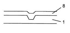
- FIGS. 1 a, bare drawings showing a glass substrate having a protective layer in accordance with present invention
- FIG. 1 arepresents a protective layer on which bubbles appear
- FIG. 1 brepresents a protective layer on which cracks occur.
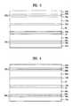
- FIG. 2is a drawing showing a liquid crystal display device having the glass substrate of the FIGS. 1 a, b.
- FIGS. 1 a, bare drawings showing a glass substrate 1 having the protective layer, as shown in FIG. 1 a, a bubble, which is formed in process of manufacturing glass and its diameter is several um—several ten um, is appeared on the thin substrate which is etched less than 0.7 mm. Further, since the thickness of the glass substrate 1 is very thin, a crack may be occured by fine mechanical impulse as shown in FIG. 1 b.
- a transparent protective layer 8 formed on the substrate 1includes a plurality of layer having an inorganic matter or an organic matter, or an inorganic matter and an organic matter, then a refractive index of each layer is 1.4 - 1.6.
- the inorganic layer 8is formed on the substrate 1 by general thin layer deposition method such as sputtering method, CVD(chemical vapor deposition) method, and evaporation method.
- organic layer 8is formed by irradiating the light such as ultraviolet, visible ray, etc., onto a thermosetting resin deposited on the substrate and curing that. At this time the inorganic matter having the compressive stress and the organic matter having the low viscosity coefficient(about several cp—several ten cp).
- the protective layer 8is formed on the bubble as well as the surface of substrate 1 , diameters of the bubbles are minimized from micrometer to angstrom. Accordingly when the substrate 1 is applied to a LCD, it is possible to prevent decreasing of an image quality by small scattering of the light in that region.
- the substrate 1is brokendown slowly according to passing of time in manufacturing process of the LCD. Further an impurity inserted in the crack cause to decrease quality of the LCD. While the inorganic layer prevent transmission of the crack by the compressive stress, and the cured organic layer also prevent transmission of the crack, thereby a strong glass substrate for mechanical impulse can be achieved.
- the protective layer 8may be one layer with an inorganic layer or an organic layer, or a plurality of layers composed of same matter or different matter.
- FIG. 2is a drawing showing a liquid crystal display device having two glass substrates including the protective layers.
- a transparent electrode 12 made of such as ITO(indium tin oxide)is formed on the first substrate.
- the transparent electrode 12is formed on the first substrate, it is possible that the transparent electrode 12 is formed on the second substrate.
- Further alignment layers 13 a, 13 b including polyimide or photo alignment materialare formed on the transparent electrode 12 , then an alignment direction of the alignment layer is determined by using a mechanical or optical method.
- a liquid crystal layer 15is formed between the first and second substrates.
- the protective layer 18 a, 18 bare an inorganic layers or an organic layers, or a plurality of layers composed of same matter or different matter and formed on outside surface of both the first substrate 10 a and the second substrate 10 b. Continually a first polarizer 14 a and a second polarizer 14 b are formed on the protective layers 18 a, 18 b.
- TFTsthin film transisters
- a color filter layeris formed on the second substrate.
- the protective layers 18 a, 18 bare formed on that, and the transparent electrode 12 is formed on the protective layer 18 a, 18 b by the sputtering method.
- the substrate 10 a, 10 bafter the passivation layers 18 a, 18 b are formed on each the glass.
- the TFTs(not illustrated)are formed on the first substrate 10 a by depositing and photoetching a metal layer, and the alignment layer 13 a, 13 b are formed by mechanical depositing or injecting the alignment material.
- the protective layerincludes an inorganic or an organic matter, the thin glass substrate through etching is bearable from a mechanical impulse.
- the protective layerprevent transmission of the crack thereby the substrate is not brokendown.
- the present inventionprovides the good quality LCD having thin glass substrate light and its surface is smooth and strong from mechanical impulse.
Landscapes
- Physics & Mathematics (AREA)
- Nonlinear Science (AREA)
- Mathematical Physics (AREA)
- Chemical & Material Sciences (AREA)
- Crystallography & Structural Chemistry (AREA)
- General Physics & Mathematics (AREA)
- Optics & Photonics (AREA)
- Liquid Crystal (AREA)
Abstract
Description
- The present invention relates to a liquid crystal display device, and more particularly to a liquid crystal display device having glass substrates uniformly and smoothly formed on its outer surface to increase the mechanical strength thereof and method of making the same.
- As a display device of a television and a personal computer, etc., a large size cathode ray tube(CRT) display device has been used. However, since the screen must be separated from the electron gun more than predetermined distance for large size screen CRT, the volume is increased. Thus, this CRT cannot be applied to the thin weight, small size, and low power consumption electronic device such as a wall-mounted television, a portable television and a notebook computer, etc.
- According to the purpose of display device, the flat panel display devices such as LCD(liquid crystal display), PDP(plasma display panel), ELD(electroluminescent display), and VFD(vacuum fluorescent display) have been introduced recently. Among above flat panel display device, the LCD has been dominantly researched for the good picture quality and low power consumption. The LCD-applied portable television and notebook computer are on the market resent, but there are also problems to be solved in this LCD yet. Particularly, the size and weight are important factor of the LCD investigation because of the apparatus have to be in hands of user.
- For small size and light LCD, there are several methods of reducing the size and weight of the LCD element. However, the driving circuit and the thin film transistor, which are necessary element of the LCD, are so thin that the weight cannot be reduced. On the other hand, it is possible to reduce the weight of the glass substrate which is a basic element of the LCD. Specially, since the glass substrate is most heavy element of the LCD, the method of reducing the weight of the glass substrate has been continuously researched.
- The light glass substrate means thin glass substrate. However, the thin glass substrate causes the damage and the surface roughness, so that the mechanical strength is weakened and the image quality of LCD is deteriorated.
- In several etching methods of reducing the thickness of the glass substrate, it is representative that the substrate is etched in a case which was filled with etchant. In this etching method, however, because of impurities created in etching process, the substrate is not uniformly etched.
- Therefore in proposed another etching method, the substrate is etched removing the impurities created in etching process by bubbles through a porous plate after a substrate is arranged.
- In this method, however, bubbles appear on the substrate, or cracks occur by mechanical impulse, the bubbles were created in process of manufacturing glass and diameters of several um—several ten um. In case that the substrate applied to a LCD desirable image quality can not be achieved because of scattering of the light in a bubble region. Further if the cracks occur on the substrate by an etching process of the glass or mechanical impulse, impurities pass into the substrate in manufacturing process of the LCD thereby a quality of the LCD is down. In addition, since the crack is intensified according to passing of time, thereby the substrate is brokendown.
- Accordingly in order to decrease weight of the LCD by etching the substrate, it is very important to decrease a fault on the substrate as well as an etching method.
- An object of the present invention is to provide the LCD having thin glass substrate which is light and its surface is smooth and strong from mechanical impulse.
- In order to achieve this object, the LCD according to present invention includes a first substrate and a second substrate, two protective layers including at least one layer formed on outer surface of the first and second substrates, a transparent electrode formed on inner surface of the first substrate or the second substrate, an alignment layer formed on the transparent electrode, and two polarizers attached on the first and second substrates.
- Each the protective layer material may be an inorganic matter having a compressive stress or an organic matter having a low viscosity coefficient, further the protective layer may be one layer including an inorganic layer or an organic layer, or a plurality of layers composed of same matter or different matter. The inorganic layer is formed by a thin layer depositing method on the substrate, while the organic layer is formed by irradiating the light such as ultraviolet, visible ray, etc., onto a thermosetting resin deposited on the substrate and curing that.
FIGS. 1 a, bare drawings showing a glass substrate having a protective layer in accordance with present invention,FIG. 1 arepresents a protective layer on which bubbles appear,FIG. 1 brepresents a protective layer on which cracks occur.FIG. 2 is a drawing showing a liquid crystal display device having the glass substrate of theFIGS. 1 a, b.- Reference will now be made in detail to the present preferred embodiments of the invention, examples of which are illustrated in the accompanying drawings.
FIGS. 1 a, bare drawings showing a glass substrate1 having the protective layer, as shown inFIG. 1 a,a bubble, which is formed in process of manufacturing glass and its diameter is several um—several ten um, is appeared on the thin substrate which is etched less than 0.7 mm. Further, since the thickness of the glass substrate1 is very thin, a crack may be occured by fine mechanical impulse as shown inFIG. 1 b.- A transparent
protective layer 8 formed on the substrate1 includes a plurality of layer having an inorganic matter or an organic matter, or an inorganic matter and an organic matter, then a refractive index of each layer is 1.4-1.6. theinorganic layer 8 is formed on the substrate1 by general thin layer deposition method such as sputtering method, CVD(chemical vapor deposition) method, and evaporation method. Whileorganic layer 8 is formed by irradiating the light such as ultraviolet, visible ray, etc., onto a thermosetting resin deposited on the substrate and curing that. At this time the inorganic matter having the compressive stress and the organic matter having the low viscosity coefficient(about several cp—several ten cp). - When bubbles appear on the surface of substrate1 as shown in
FIG. 1 a,an desirable image quality can not be achived because of scattering of the light in a bubble region. - Since the
protective layer 8 is formed on the bubble as well as the surface of substrate1, diameters of the bubbles are minimized from micrometer to angstrom. Accordingly when the substrate1 is applied to a LCD, it is possible to prevent decreasing of an image quality by small scattering of the light in that region. - Additionally if cracks occur on the substrate1 as shown in
FIG. 1 b,the substrate1 is brokendown slowly according to passing of time in manufacturing process of the LCD. Further an impurity inserted in the crack cause to decrease quality of the LCD. While the inorganic layer prevent transmission of the crack by the compressive stress, and the cured organic layer also prevent transmission of the crack, thereby a strong glass substrate for mechanical impulse can be achieved. - The
protective layer 8 may be one layer with an inorganic layer or an organic layer, or a plurality of layers composed of same matter or different matter. FIG. 2 is a drawing showing a liquid crystal display device having two glass substrates including the protective layers.- Each thickness of a
first substrate 10aand asecond substrate 10bis less than 0.7 mm, atransparent electrode 12 made of such as ITO(indium tin oxide) is formed on the first substrate. In present embodiment, although, thetransparent electrode 12 is formed on the first substrate, it is possible that thetransparent electrode 12 is formed on the second substrate.Further alignment layers transparent electrode 12, then an alignment direction of the alignment layer is determined by using a mechanical or optical method. On the other hand aliquid crystal layer 15 is formed between the first and second substrates. Theprotective layer first substrate 10aand thesecond substrate 10b.Continually afirst polarizer 14aand asecond polarizer 14bare formed on theprotective layers - Although not showing with drawing, TFTs(thin film transisters) are formed on the
first substrate 10a,and a color filter layer is formed on the second substrate. - After etching, grinding and scribing two glasses by general etching method, the
protective layers transparent electrode 12 is formed on theprotective layer substrate passivation layers first substrate 10aby depositing and photoetching a metal layer, and thealignment layer second substrate - In the above-discussed structure, since the protective layer includes an inorganic or an organic matter, the thin glass substrate through etching is bearable from a mechanical impulse.
- Further in etching process, since the inorganic or organic matter have diameters of the bubbles which a quality of the LCD is down by that decreased, it is possible to achieve the good quality LCD having soft and uniform surface.
- When cracks occur on the substrate, the protective layer prevent transmission of the crack thereby the substrate is not brokendown.
- As a result, the present invention provides the good quality LCD having thin glass substrate light and its surface is smooth and strong from mechanical impulse.
- Other embodiments of the invention will be apparent to those skilled in the art from consideration of the specification and practice of the invention disclosed herein. It is intended that the specification and examples be considered as exemplary only, with a true scope and spirit of the invention being indicated by the following claims.
Claims (7)
1-16. (canceled)
17. A method of manufacturing a thin glass substrate of a liquid crystal display device, comprising the steps of:
providing a glass;
forming a substrate by processing the glass; and
forming a protective layer on the glass substrate.
18-19. (canceled)
20. The method according toclaim 17 , wherein the step of forming the protective layer includes the step of irradiating the light after depositing an organic matter on the glass substrate.
21. The method according toclaim 20 , wherein the light is an ultraviolet or a visible ray.
22. The method according toclaim 17 , wherein the step of forming the protective layer includes the step of coating an inorganic matter on the glass substrate.
23-27. (canceled)
Priority Applications (1)
| Application Number | Priority Date | Filing Date | Title |
|---|---|---|---|
| US11/192,172US20050271835A1 (en) | 1997-10-20 | 2005-07-29 | Liquid crystal display device having thin glass substrate on which protective layer formed and method of making the same |
Applications Claiming Priority (3)
| Application Number | Priority Date | Filing Date | Title |
|---|---|---|---|
| US08/954,124US6327011B2 (en) | 1997-10-20 | 1997-10-20 | Liquid crystal display device having thin glass substrate on which protective layer formed and method of making the same |
| US09/964,739US6955840B2 (en) | 1997-10-20 | 2001-09-28 | Liquid crystal display device having thin glass substrate on which protective layer formed and method of making the same |
| US11/192,172US20050271835A1 (en) | 1997-10-20 | 2005-07-29 | Liquid crystal display device having thin glass substrate on which protective layer formed and method of making the same |
Related Parent Applications (1)
| Application Number | Title | Priority Date | Filing Date |
|---|---|---|---|
| US09/964,739DivisionUS6955840B2 (en) | 1997-10-20 | 2001-09-28 | Liquid crystal display device having thin glass substrate on which protective layer formed and method of making the same |
Publications (1)
| Publication Number | Publication Date |
|---|---|
| US20050271835A1true US20050271835A1 (en) | 2005-12-08 |
Family
ID=25494963
Family Applications (3)
| Application Number | Title | Priority Date | Filing Date |
|---|---|---|---|
| US08/954,124Expired - LifetimeUS6327011B2 (en) | 1997-10-20 | 1997-10-20 | Liquid crystal display device having thin glass substrate on which protective layer formed and method of making the same |
| US09/964,739Expired - LifetimeUS6955840B2 (en) | 1997-10-20 | 2001-09-28 | Liquid crystal display device having thin glass substrate on which protective layer formed and method of making the same |
| US11/192,172AbandonedUS20050271835A1 (en) | 1997-10-20 | 2005-07-29 | Liquid crystal display device having thin glass substrate on which protective layer formed and method of making the same |
Family Applications Before (2)
| Application Number | Title | Priority Date | Filing Date |
|---|---|---|---|
| US08/954,124Expired - LifetimeUS6327011B2 (en) | 1997-10-20 | 1997-10-20 | Liquid crystal display device having thin glass substrate on which protective layer formed and method of making the same |
| US09/964,739Expired - LifetimeUS6955840B2 (en) | 1997-10-20 | 2001-09-28 | Liquid crystal display device having thin glass substrate on which protective layer formed and method of making the same |
Country Status (1)
| Country | Link |
|---|---|
| US (3) | US6327011B2 (en) |
Cited By (2)
| Publication number | Priority date | Publication date | Assignee | Title |
|---|---|---|---|---|
| US7532274B2 (en) | 2005-12-26 | 2009-05-12 | Hitachi Displays, Ltd. | Liquid crystal display and display |
| US20200096673A1 (en)* | 2018-09-26 | 2020-03-26 | Innolux Corporation | Method for manufacturing electronic device |
Families Citing this family (75)
| Publication number | Priority date | Publication date | Assignee | Title |
|---|---|---|---|---|
| US6327011B2 (en)* | 1997-10-20 | 2001-12-04 | Lg Electronics, Inc. | Liquid crystal display device having thin glass substrate on which protective layer formed and method of making the same |
| US7808479B1 (en) | 2003-09-02 | 2010-10-05 | Apple Inc. | Ambidextrous mouse |
| JP3773723B2 (en)* | 1999-01-29 | 2006-05-10 | シャープ株式会社 | Liquid crystal display |
| KR100652041B1 (en)* | 2000-12-29 | 2006-11-30 | 엘지.필립스 엘시디 주식회사 | LCD and its manufacturing method |
| US7109653B2 (en)* | 2002-01-15 | 2006-09-19 | Seiko Epson Corporation | Sealing structure with barrier membrane for electronic element, display device, electronic apparatus, and fabrication method for electronic element |
| US7656393B2 (en) | 2005-03-04 | 2010-02-02 | Apple Inc. | Electronic device having display and surrounding touch sensitive bezel for user interface and control |
| US11275405B2 (en) | 2005-03-04 | 2022-03-15 | Apple Inc. | Multi-functional hand-held device |
| JP4128910B2 (en)* | 2003-06-11 | 2008-07-30 | 日本アイ・ビー・エム株式会社 | Liquid crystal display cell and method of manufacturing liquid crystal display cell |
| KR100599704B1 (en)* | 2003-10-21 | 2006-07-12 | 삼성에스디아이 주식회사 | Plasma display panel |
| US7812827B2 (en) | 2007-01-03 | 2010-10-12 | Apple Inc. | Simultaneous sensing arrangement |
| US8493331B2 (en) | 2007-06-13 | 2013-07-23 | Apple Inc. | Touch detection using multiple simultaneous frequencies |
| CN101178501B (en)* | 2007-10-16 | 2010-12-15 | 长兴化学工业股份有限公司 | optical sheet with reinforced structure |
| TWI354153B (en)* | 2007-11-19 | 2011-12-11 | Au Optronics Corp | Flat display panel having strength enhancing struc |
| TWI327103B (en)* | 2007-11-21 | 2010-07-11 | Au Optronics Corp | Thin substrate, manufacturing process thereof, and manufacturing process of display panel applying the same |
| US8673163B2 (en)* | 2008-06-27 | 2014-03-18 | Apple Inc. | Method for fabricating thin sheets of glass |
| US7810355B2 (en) | 2008-06-30 | 2010-10-12 | Apple Inc. | Full perimeter chemical strengthening of substrates |
| US10031549B2 (en) | 2008-07-10 | 2018-07-24 | Apple Inc. | Transitioning between modes of input |
| US20100006350A1 (en)* | 2008-07-11 | 2010-01-14 | Elias John G | Stylus Adapted For Low Resolution Touch Sensor Panels |
| US8300019B2 (en) | 2008-07-15 | 2012-10-30 | Apple Inc. | Capacitive sensor coupling correction |
| US9335868B2 (en)* | 2008-07-31 | 2016-05-10 | Apple Inc. | Capacitive sensor behind black mask |
| US8743091B2 (en)* | 2008-07-31 | 2014-06-03 | Apple Inc. | Acoustic multi-touch sensor panel |
| US8659556B2 (en)* | 2008-09-10 | 2014-02-25 | Apple Inc. | Advanced receive channel architecture |
| US8592697B2 (en) | 2008-09-10 | 2013-11-26 | Apple Inc. | Single-chip multi-stimulus sensor controller |
| US8237667B2 (en) | 2008-09-10 | 2012-08-07 | Apple Inc. | Phase compensation for multi-stimulus controller |
| US9348451B2 (en)* | 2008-09-10 | 2016-05-24 | Apple Inc. | Channel scan architecture for multiple stimulus multi-touch sensor panels |
| US9189048B2 (en)* | 2008-09-10 | 2015-11-17 | Apple Inc. | Circuit having a low power mode |
| US9606663B2 (en)* | 2008-09-10 | 2017-03-28 | Apple Inc. | Multiple stimulation phase determination |
| US7978281B2 (en)* | 2008-09-16 | 2011-07-12 | General Dynamics Land Systems | Low stress mounting support for ruggedized displays |
| US20100066683A1 (en)* | 2008-09-17 | 2010-03-18 | Shih-Chang Chang | Method for Transferring Thin Film to Substrate |
| US20100215873A1 (en)* | 2008-10-10 | 2010-08-26 | Tpo Displays Corp. | System for display images and fabrication method of display panels |
| US9063605B2 (en) | 2009-01-09 | 2015-06-23 | Apple Inc. | Thin glass processing using a carrier |
| US7918019B2 (en)* | 2009-01-09 | 2011-04-05 | Apple Inc. | Method for fabricating thin touch sensor panels |
| CN102388003B (en) | 2009-03-02 | 2014-11-19 | 苹果公司 | Technology for Strengthening Glass Covers for Portable Electronic Devices |
| US20110006998A1 (en)* | 2009-07-10 | 2011-01-13 | Sunggu Kang | Patterning of thin film conductive and passivation layers |
| US8654524B2 (en) | 2009-08-17 | 2014-02-18 | Apple Inc. | Housing as an I/O device |
| US8475872B2 (en)* | 2009-08-19 | 2013-07-02 | Apple Inc. | Patterning of thin film layers |
| KR101618157B1 (en)* | 2009-12-21 | 2016-05-09 | 삼성디스플레이 주식회사 | Display device and method for manufacturing the display device |
| US9778685B2 (en) | 2011-05-04 | 2017-10-03 | Apple Inc. | Housing for portable electronic device with reduced border region |
| US9213451B2 (en) | 2010-06-04 | 2015-12-15 | Apple Inc. | Thin glass for touch panel sensors and methods therefor |
| US10189743B2 (en) | 2010-08-18 | 2019-01-29 | Apple Inc. | Enhanced strengthening of glass |
| US8824140B2 (en) | 2010-09-17 | 2014-09-02 | Apple Inc. | Glass enclosure |
| US20120075252A1 (en) | 2010-09-23 | 2012-03-29 | Microsoft Corporation | Ruggedized display device |
| US8950215B2 (en) | 2010-10-06 | 2015-02-10 | Apple Inc. | Non-contact polishing techniques for reducing roughness on glass surfaces |
| US9725359B2 (en) | 2011-03-16 | 2017-08-08 | Apple Inc. | Electronic device having selectively strengthened glass |
| US10781135B2 (en) | 2011-03-16 | 2020-09-22 | Apple Inc. | Strengthening variable thickness glass |
| US9128666B2 (en) | 2011-05-04 | 2015-09-08 | Apple Inc. | Housing for portable electronic device with reduced border region |
| US9944554B2 (en) | 2011-09-15 | 2018-04-17 | Apple Inc. | Perforated mother sheet for partial edge chemical strengthening and method therefor |
| US9516149B2 (en) | 2011-09-29 | 2016-12-06 | Apple Inc. | Multi-layer transparent structures for electronic device housings |
| US10144669B2 (en) | 2011-11-21 | 2018-12-04 | Apple Inc. | Self-optimizing chemical strengthening bath for glass |
| US10133156B2 (en) | 2012-01-10 | 2018-11-20 | Apple Inc. | Fused opaque and clear glass for camera or display window |
| US8773848B2 (en) | 2012-01-25 | 2014-07-08 | Apple Inc. | Fused glass device housings |
| KR101881000B1 (en) | 2012-04-27 | 2018-07-24 | 삼성전자주식회사 | Portable terminal with crack prevention structure for display device |
| US9176604B2 (en) | 2012-07-27 | 2015-11-03 | Apple Inc. | Stylus device |
| US9946302B2 (en) | 2012-09-19 | 2018-04-17 | Apple Inc. | Exposed glass article with inner recessed area for portable electronic device housing |
| US9459661B2 (en) | 2013-06-19 | 2016-10-04 | Apple Inc. | Camouflaged openings in electronic device housings |
| KR102083987B1 (en)* | 2013-06-20 | 2020-03-04 | 삼성디스플레이 주식회사 | Back palne of flat panel display and method for manufacturing the same |
| US8988390B1 (en) | 2013-07-03 | 2015-03-24 | Apple Inc. | Frequency agile touch processing |
| US20160216558A1 (en)* | 2013-09-09 | 2016-07-28 | Empire Technology Development Llc | Strengthened glass substrates for polarizers and color filters |
| TWI510574B (en) | 2013-11-18 | 2015-12-01 | Eternal Materials Co Ltd | Organic-inorganic composite resin, coating composition containing the same and application thereof |
| US9886062B2 (en) | 2014-02-28 | 2018-02-06 | Apple Inc. | Exposed glass article with enhanced stiffness for portable electronic device housing |
| US11036318B2 (en) | 2015-09-30 | 2021-06-15 | Apple Inc. | Capacitive touch or proximity detection for crown |
| US10671222B2 (en) | 2015-09-30 | 2020-06-02 | Apple Inc. | Touch sensor pattern for edge input detection |
| US11402950B2 (en) | 2016-07-29 | 2022-08-02 | Apple Inc. | Methodology and application of acoustic touch detection |
| US10606418B2 (en) | 2017-03-31 | 2020-03-31 | Apple Inc. | Ultrasonic touch detection on stylus |
| US11157115B2 (en) | 2017-03-31 | 2021-10-26 | Apple Inc. | Composite cover material for sensitivity improvement of ultrasonic touch screens |
| US11144158B2 (en) | 2017-05-24 | 2021-10-12 | Apple Inc. | Differential acoustic touch and force sensing |
| US11334196B2 (en) | 2017-05-24 | 2022-05-17 | Apple Inc. | System and method for acoustic touch and force sensing |
| CN108932084B (en) | 2017-05-24 | 2022-05-27 | 苹果公司 | Systems and methods for acoustic touch and force sensing |
| WO2018222247A1 (en) | 2017-06-02 | 2018-12-06 | Apple Inc. | Device, method, and graphical user interface for annotating content |
| US10949030B2 (en) | 2017-09-26 | 2021-03-16 | Apple Inc. | Shear-poled curved piezoelectric material |
| US10802651B2 (en) | 2018-01-30 | 2020-10-13 | Apple Inc. | Ultrasonic touch detection through display |
| US11366552B2 (en) | 2018-02-06 | 2022-06-21 | Apple, Inc. | Ultrasonic polarizer |
| US12340034B2 (en) | 2018-06-01 | 2025-06-24 | Apple Inc. | Devices, methods, and graphical user interfaces for an electronic device interacting with a stylus |
| US10725573B2 (en) | 2018-08-06 | 2020-07-28 | Apple Inc. | Annular piezoelectric structure for ultrasonic touch sensing |
| US12216851B2 (en) | 2022-09-23 | 2025-02-04 | Apple Inc. | Multi-directional texture based input device |
Citations (65)
| Publication number | Priority date | Publication date | Assignee | Title |
|---|---|---|---|---|
| US3689333A (en)* | 1970-08-24 | 1972-09-05 | Tasope Ltd | Etching machine and method for making printing plates |
| US3756898A (en)* | 1969-07-14 | 1973-09-04 | Buckbee Mears Co | Resistant system suitable for controlling etching without the aid of an etchant |
| US3869313A (en)* | 1973-05-21 | 1975-03-04 | Allied Chem | Apparatus for automatic chemical processing of workpieces, especially semi-conductors |
| US4125594A (en)* | 1976-12-22 | 1978-11-14 | Corning Glass Works | Purification of hydrofluoric acid etching solutions with weak anion exchange resins |
| US4147581A (en)* | 1976-03-29 | 1979-04-03 | Philip A. Hunt Chemical Corp. | Etching of metal |
| US4240880A (en)* | 1978-07-25 | 1980-12-23 | Sumitomo Metal Mining Co., Ltd. | Method and apparatus for selectively plating a material |
| US4332649A (en)* | 1979-12-07 | 1982-06-01 | Saelzle Erich | Method of polishing glass ware with sulfuric acid and hydrofluoric acid |
| US4341841A (en)* | 1978-11-13 | 1982-07-27 | Nhk Spring Co., Ltd. | Multi-layer coating protective film form |
| US4431683A (en)* | 1981-04-24 | 1984-02-14 | Hitachi, Ltd. | Process for producing transparent electroconductive film |
| US4482425A (en)* | 1983-06-27 | 1984-11-13 | Psi Star, Inc. | Liquid etching reactor and method |
| US4501636A (en)* | 1983-12-28 | 1985-02-26 | The United States Of America As Represented By The Secretary Of The Air Force | Apparatus for etching vertical junction solar cell wafers |
| US4624729A (en)* | 1984-10-30 | 1986-11-25 | Vitreal Specchi S.P.A. | Machine for continuously etching a surface of glass sheets |
| US4671814A (en)* | 1985-03-08 | 1987-06-09 | Central Glass Company | Method of strengthening glass article formed of float glass by ion exchange |
| US4715686A (en)* | 1984-11-16 | 1987-12-29 | Seiko Epson Corporation | Light-passive display device and method of manufacturing same |
| US4826556A (en)* | 1987-10-01 | 1989-05-02 | Nippon Scientific Co., Ltd. | Plastic mold decapsuling apparatus |
| US4846868A (en)* | 1986-09-05 | 1989-07-11 | Central Glass Company, Limited | Chemically strengthened glass article and method of producing same |
| US4886590A (en)* | 1987-11-02 | 1989-12-12 | Man-Gill Chemical Company | Chemical process control system |
| US4953952A (en)* | 1985-05-02 | 1990-09-04 | Sumitomo Chemical Company, Ltd. | Color liquid crystal displaying panels |
| US4980017A (en)* | 1988-10-01 | 1990-12-25 | Nisso Engineering Company, Ltd. | Method for recirculating high-temperature etching solution |
| US5000795A (en)* | 1989-06-16 | 1991-03-19 | At&T Bell Laboratories | Semiconductor wafer cleaning method and apparatus |
| US5002627A (en)* | 1988-08-12 | 1991-03-26 | International Business Machines Corporation | Spray etching apparatus with automatic individually controllable etching jets |
| US5034061A (en)* | 1990-03-15 | 1991-07-23 | General Electric Company | Transparent shatter-resistant silicone coating |
| US5082518A (en)* | 1990-10-29 | 1992-01-21 | Submicron Systems, Inc. | Sparger plate for ozone gas diffusion |
| US5112437A (en)* | 1990-02-20 | 1992-05-12 | Dainippon Screen Mfg. Co., Ltd. | Oxide film removing apparatus and removing method thereof using azeotropic vapor mixture |
| US5112453A (en)* | 1990-10-31 | 1992-05-12 | Behr Omri M | Method and apparatus for producing etched plates for graphic printing |
| US5159787A (en)* | 1989-01-20 | 1992-11-03 | Nkk Corporation | Method for lapping two surfaces of a titanium disk |
| US5164018A (en)* | 1992-03-18 | 1992-11-17 | Barcelona Jr Russell L | Water-spot remover containing hydrofluoric acid, ammonium fluoride, and an alcohol |
| US5246540A (en)* | 1992-04-01 | 1993-09-21 | Tru Vue, Inc. | Apparatus and method for etching glass |
| US5251980A (en)* | 1990-12-14 | 1993-10-12 | Anritsu Corporation | Sensing system for measuring specific value of substance to be measured by utilizing change in thermal resistance |
| US5260157A (en)* | 1989-10-20 | 1993-11-09 | Mita Industrial Co., Ltd. | Electrophotographic photosensitive element comprising a surface protective layer comprising an etherified melamine-formaldehyde resin |
| US5260174A (en)* | 1989-02-17 | 1993-11-09 | Dai Nippon Insatsu Kabushiki Kaisha | Method and apparatus for forming a coating of a viscous liquid on an object |
| US5277715A (en)* | 1992-06-04 | 1994-01-11 | Micron Semiconductor, Inc. | Method of reducing particulate concentration in process fluids |
| US5319479A (en)* | 1990-09-04 | 1994-06-07 | Ricoh Company, Ltd. | Deposited multi-layer device with a plastic substrate having an inorganic thin film layer |
| US5371619A (en)* | 1992-04-30 | 1994-12-06 | Apple Computer, Inc. | Optically coupled liquid crystal cell with grease |
| US5378308A (en)* | 1992-11-09 | 1995-01-03 | Bmc Industries, Inc. | Etchant distribution apparatus |
| US5389148A (en)* | 1993-01-28 | 1995-02-14 | Nordson Corporation | Spray apparatus utilizing porous sheet |
| US5403616A (en)* | 1992-10-27 | 1995-04-04 | Matsushita Electric Industrial Co., Ltd. | Method for forming patterned transparent conducting film |
| US5424876A (en)* | 1991-10-31 | 1995-06-13 | Asahi Kogaku Kogyo Kabushiki Kaisha | Surface reflecting mirror having a silicon dioxide under layer |
| US5429711A (en)* | 1992-09-18 | 1995-07-04 | Mitsubishi Materials Corporation | Method for manufacturing wafer |
| US5434433A (en)* | 1992-08-19 | 1995-07-18 | Seiko Instruments Inc. | Semiconductor device for a light wave |
| US5437896A (en)* | 1993-07-06 | 1995-08-01 | U.S. Philips Corporation | Method of preparing a composite material of silica network and chains of a polyhydroxy compound and a liquid crystal display device incorporating such composite material |
| US5505804A (en)* | 1993-12-24 | 1996-04-09 | Sharp Kabushiki Kaisha | Method of producing a condenser lens substrate |
| US5514850A (en)* | 1992-06-30 | 1996-05-07 | Sharp Kabushiki Kaisha | Defect compensation method for smoothing a surface of a transparent plate with an ArF excimer laser beam |
| US5540784A (en)* | 1994-09-23 | 1996-07-30 | United Laboratories, Inc. | Pressurized closed flow cleaning system |
| US5543181A (en)* | 1993-12-16 | 1996-08-06 | Degussa Aktiengesellschaft | Process and device for defined impregnation of honeycomb structures with parallel flow channels |
| US5606438A (en)* | 1994-06-11 | 1997-02-25 | Motorola, Inc. | Rugged liquid crystal display and method of manufacture |
| US5637353A (en)* | 1990-09-27 | 1997-06-10 | Monsanto Company | Abrasion wear resistant coated substrate product |
| US5654057A (en)* | 1994-12-28 | 1997-08-05 | Hoya Corporation | Sheet glass flattening method, method of manufacturing glass substrate for an information recording disk using flattened glass, method of manufacturing a magnetic recording disk using glass substrate, and magnetic recording medium |
| US5701165A (en)* | 1994-07-05 | 1997-12-23 | Sharp Kabushiki Kaisha | Projection-type liquid crystal display with a liquid crystal panel having a reflection-reducing coating layer |
| US5715022A (en)* | 1989-07-19 | 1998-02-03 | Sharp Kabushiki Kaisha | Image display apparatus |
| US5721601A (en)* | 1994-09-29 | 1998-02-24 | Sanyo Electric Co., Ltd. | Display units having two insolating films and a planarizing film and process for producing the same |
| US5766493A (en)* | 1995-07-06 | 1998-06-16 | Lg Electronics Inc. | Method of fabricating a liquid crystal display substrate |
| US5767931A (en)* | 1995-10-24 | 1998-06-16 | Lucent Technologies Inc. | Composite for plastic liquid crystal display |
| US5781255A (en)* | 1992-06-08 | 1998-07-14 | Hitachi, Ltd. | Active matrix display device using aluminum alloy in scanning signal line or video signal line |
| US5784137A (en)* | 1995-02-17 | 1998-07-21 | Sharp Kabushiki Kaisha | Liquid crystal display device and method for producing the same |
| US5788871A (en)* | 1995-12-26 | 1998-08-04 | Lg Semicon Co., Ltd. | Etch-ending point measuring method for wet-etch process |
| US5808715A (en)* | 1997-03-27 | 1998-09-15 | Industrial Technology Research Institute | Liquid crystal display devices having undercoat and overcoat made of TiO2 --SiO2 composite material |
| US5818559A (en)* | 1995-09-26 | 1998-10-06 | Fuji Photo Film Co., Ltd. | Liquid crystal display having different linear expansion coefficients among the materials of the display |
| US5819434A (en)* | 1996-04-25 | 1998-10-13 | Applied Materials, Inc. | Etch enhancement using an improved gas distribution plate |
| US5835176A (en)* | 1997-07-29 | 1998-11-10 | Lg Electronics, Inc. | Method for planarizing a substrate of a liquid crystal display |
| US5917571A (en)* | 1996-06-03 | 1999-06-29 | Sharp Kabushiki Kaisha | Active matrix substrate having benzocyclobutene-containing interlayer insulating film and method for fabricating same |
| US6327011B2 (en)* | 1997-10-20 | 2001-12-04 | Lg Electronics, Inc. | Liquid crystal display device having thin glass substrate on which protective layer formed and method of making the same |
| US6614493B1 (en)* | 1996-11-27 | 2003-09-02 | Lg. Philips Lcd Co., Ltd. | Liquid crystal display and method of manufacturing the same |
| US6853433B2 (en)* | 2002-11-11 | 2005-02-08 | Lg. Philips Lcd Co., Ltd. | Liquid crystal display device having soda-lime glass and method of fabricating the same |
| US6873391B2 (en)* | 2000-10-23 | 2005-03-29 | Lg. Philips Lcd Co., Ltd. | LCD panel and method for fabricating the same |
Family Cites Families (22)
| Publication number | Priority date | Publication date | Assignee | Title |
|---|---|---|---|---|
| GB829605A (en) | 1957-02-18 | 1960-03-02 | Corning Glass Works | Method of regenerating a glass etching bath |
| FR1200180A (en) | 1957-02-18 | 1959-12-18 | Corning Glass Works | Process for the regeneration of glass etching baths |
| DE1920009B2 (en) | 1969-04-19 | 1971-11-11 | Dunchen, Hannes, 3340 Wolfen buttel | METHOD AND DEVICE FOR TREATMENT OF SOLID POLISHING ACID |
| JPS60163435A (en) | 1984-02-03 | 1985-08-26 | Toshiba Corp | Semiconductor wafer cleaning equipment |
| GB2178894B (en) | 1985-08-06 | 1988-07-27 | Gen Electric Co Plc | Preparation of fragile devices |
| GB2178895B (en) | 1985-08-06 | 1988-11-23 | Gen Electric Co Plc | Improved preparation of fragile devices |
| DE3611387A1 (en) | 1986-04-04 | 1987-10-15 | Semax Gmbh Prozesstechnik | Installation and method for producing integrated circuits or the like from silicon or from gallium arsenide wafers or the like |
| JPH0630351B2 (en) | 1987-03-31 | 1994-04-20 | 株式会社東芝 | Cleaning end point determination method for semiconductor manufacturing equipment |
| JPH01189631A (en) | 1988-01-26 | 1989-07-28 | Seiko Epson Corp | Production of liquid crystal panel electrode |
| JPH02138459A (en) | 1988-11-16 | 1990-05-28 | Raimuzu:Kk | Laminated hard material and production thereof |
| JP2786865B2 (en) | 1988-11-24 | 1998-08-13 | 大日本印刷株式会社 | Manufacturing method of color filter |
| JP2678044B2 (en) | 1989-01-25 | 1997-11-17 | 松下電器産業株式会社 | Active matrix substrate manufacturing method |
| JPH0679512B2 (en) | 1989-06-20 | 1994-10-05 | シャープ株式会社 | Method for manufacturing thin film EL panel |
| US6067062A (en) | 1990-09-05 | 2000-05-23 | Seiko Instruments Inc. | Light valve device |
| JP2722798B2 (en) | 1990-09-07 | 1998-03-09 | カシオ計算機株式会社 | Method for manufacturing thin liquid crystal display element |
| JP2963529B2 (en) | 1990-10-29 | 1999-10-18 | シャープ株式会社 | Active matrix display device |
| JPH0561011A (en) | 1991-09-03 | 1993-03-12 | Rohm Co Ltd | Method for manufacturing liquid crystal display element |
| JP2678326B2 (en) | 1992-03-06 | 1997-11-17 | カシオ計算機株式会社 | Manufacturing method of liquid crystal display element |
| JP2678325B2 (en) | 1992-03-06 | 1997-11-17 | カシオ計算機株式会社 | Manufacturing method of liquid crystal display element |
| KR950011951B1 (en)* | 1992-12-04 | 1995-10-12 | 삼성전관주식회사 | LCD and its manufacturing method |
| JPH07168172A (en) | 1993-12-16 | 1995-07-04 | Canon Inc | Liquid crystal display device and manufacturing method thereof |
| US5990992A (en)* | 1997-03-18 | 1999-11-23 | Nippon Sheet Glass Co., Ltd. | Image display device with plural planar microlens arrays |
- 1997
- 1997-10-20USUS08/954,124patent/US6327011B2/ennot_activeExpired - Lifetime
- 2001
- 2001-09-28USUS09/964,739patent/US6955840B2/ennot_activeExpired - Lifetime
- 2005
- 2005-07-29USUS11/192,172patent/US20050271835A1/ennot_activeAbandoned
Patent Citations (65)
| Publication number | Priority date | Publication date | Assignee | Title |
|---|---|---|---|---|
| US3756898A (en)* | 1969-07-14 | 1973-09-04 | Buckbee Mears Co | Resistant system suitable for controlling etching without the aid of an etchant |
| US3689333A (en)* | 1970-08-24 | 1972-09-05 | Tasope Ltd | Etching machine and method for making printing plates |
| US3869313A (en)* | 1973-05-21 | 1975-03-04 | Allied Chem | Apparatus for automatic chemical processing of workpieces, especially semi-conductors |
| US4147581A (en)* | 1976-03-29 | 1979-04-03 | Philip A. Hunt Chemical Corp. | Etching of metal |
| US4125594A (en)* | 1976-12-22 | 1978-11-14 | Corning Glass Works | Purification of hydrofluoric acid etching solutions with weak anion exchange resins |
| US4240880A (en)* | 1978-07-25 | 1980-12-23 | Sumitomo Metal Mining Co., Ltd. | Method and apparatus for selectively plating a material |
| US4341841A (en)* | 1978-11-13 | 1982-07-27 | Nhk Spring Co., Ltd. | Multi-layer coating protective film form |
| US4332649A (en)* | 1979-12-07 | 1982-06-01 | Saelzle Erich | Method of polishing glass ware with sulfuric acid and hydrofluoric acid |
| US4431683A (en)* | 1981-04-24 | 1984-02-14 | Hitachi, Ltd. | Process for producing transparent electroconductive film |
| US4482425A (en)* | 1983-06-27 | 1984-11-13 | Psi Star, Inc. | Liquid etching reactor and method |
| US4501636A (en)* | 1983-12-28 | 1985-02-26 | The United States Of America As Represented By The Secretary Of The Air Force | Apparatus for etching vertical junction solar cell wafers |
| US4624729A (en)* | 1984-10-30 | 1986-11-25 | Vitreal Specchi S.P.A. | Machine for continuously etching a surface of glass sheets |
| US4715686A (en)* | 1984-11-16 | 1987-12-29 | Seiko Epson Corporation | Light-passive display device and method of manufacturing same |
| US4671814A (en)* | 1985-03-08 | 1987-06-09 | Central Glass Company | Method of strengthening glass article formed of float glass by ion exchange |
| US4953952A (en)* | 1985-05-02 | 1990-09-04 | Sumitomo Chemical Company, Ltd. | Color liquid crystal displaying panels |
| US4846868A (en)* | 1986-09-05 | 1989-07-11 | Central Glass Company, Limited | Chemically strengthened glass article and method of producing same |
| US4826556A (en)* | 1987-10-01 | 1989-05-02 | Nippon Scientific Co., Ltd. | Plastic mold decapsuling apparatus |
| US4886590A (en)* | 1987-11-02 | 1989-12-12 | Man-Gill Chemical Company | Chemical process control system |
| US5002627A (en)* | 1988-08-12 | 1991-03-26 | International Business Machines Corporation | Spray etching apparatus with automatic individually controllable etching jets |
| US4980017A (en)* | 1988-10-01 | 1990-12-25 | Nisso Engineering Company, Ltd. | Method for recirculating high-temperature etching solution |
| US5159787A (en)* | 1989-01-20 | 1992-11-03 | Nkk Corporation | Method for lapping two surfaces of a titanium disk |
| US5260174A (en)* | 1989-02-17 | 1993-11-09 | Dai Nippon Insatsu Kabushiki Kaisha | Method and apparatus for forming a coating of a viscous liquid on an object |
| US5000795A (en)* | 1989-06-16 | 1991-03-19 | At&T Bell Laboratories | Semiconductor wafer cleaning method and apparatus |
| US5715022A (en)* | 1989-07-19 | 1998-02-03 | Sharp Kabushiki Kaisha | Image display apparatus |
| US5260157A (en)* | 1989-10-20 | 1993-11-09 | Mita Industrial Co., Ltd. | Electrophotographic photosensitive element comprising a surface protective layer comprising an etherified melamine-formaldehyde resin |
| US5112437A (en)* | 1990-02-20 | 1992-05-12 | Dainippon Screen Mfg. Co., Ltd. | Oxide film removing apparatus and removing method thereof using azeotropic vapor mixture |
| US5034061A (en)* | 1990-03-15 | 1991-07-23 | General Electric Company | Transparent shatter-resistant silicone coating |
| US5319479A (en)* | 1990-09-04 | 1994-06-07 | Ricoh Company, Ltd. | Deposited multi-layer device with a plastic substrate having an inorganic thin film layer |
| US5637353A (en)* | 1990-09-27 | 1997-06-10 | Monsanto Company | Abrasion wear resistant coated substrate product |
| US5082518A (en)* | 1990-10-29 | 1992-01-21 | Submicron Systems, Inc. | Sparger plate for ozone gas diffusion |
| US5112453A (en)* | 1990-10-31 | 1992-05-12 | Behr Omri M | Method and apparatus for producing etched plates for graphic printing |
| US5251980A (en)* | 1990-12-14 | 1993-10-12 | Anritsu Corporation | Sensing system for measuring specific value of substance to be measured by utilizing change in thermal resistance |
| US5424876A (en)* | 1991-10-31 | 1995-06-13 | Asahi Kogaku Kogyo Kabushiki Kaisha | Surface reflecting mirror having a silicon dioxide under layer |
| US5164018A (en)* | 1992-03-18 | 1992-11-17 | Barcelona Jr Russell L | Water-spot remover containing hydrofluoric acid, ammonium fluoride, and an alcohol |
| US5246540A (en)* | 1992-04-01 | 1993-09-21 | Tru Vue, Inc. | Apparatus and method for etching glass |
| US5371619A (en)* | 1992-04-30 | 1994-12-06 | Apple Computer, Inc. | Optically coupled liquid crystal cell with grease |
| US5277715A (en)* | 1992-06-04 | 1994-01-11 | Micron Semiconductor, Inc. | Method of reducing particulate concentration in process fluids |
| US5781255A (en)* | 1992-06-08 | 1998-07-14 | Hitachi, Ltd. | Active matrix display device using aluminum alloy in scanning signal line or video signal line |
| US5514850A (en)* | 1992-06-30 | 1996-05-07 | Sharp Kabushiki Kaisha | Defect compensation method for smoothing a surface of a transparent plate with an ArF excimer laser beam |
| US5434433A (en)* | 1992-08-19 | 1995-07-18 | Seiko Instruments Inc. | Semiconductor device for a light wave |
| US5429711A (en)* | 1992-09-18 | 1995-07-04 | Mitsubishi Materials Corporation | Method for manufacturing wafer |
| US5403616A (en)* | 1992-10-27 | 1995-04-04 | Matsushita Electric Industrial Co., Ltd. | Method for forming patterned transparent conducting film |
| US5378308A (en)* | 1992-11-09 | 1995-01-03 | Bmc Industries, Inc. | Etchant distribution apparatus |
| US5389148A (en)* | 1993-01-28 | 1995-02-14 | Nordson Corporation | Spray apparatus utilizing porous sheet |
| US5437896A (en)* | 1993-07-06 | 1995-08-01 | U.S. Philips Corporation | Method of preparing a composite material of silica network and chains of a polyhydroxy compound and a liquid crystal display device incorporating such composite material |
| US5543181A (en)* | 1993-12-16 | 1996-08-06 | Degussa Aktiengesellschaft | Process and device for defined impregnation of honeycomb structures with parallel flow channels |
| US5505804A (en)* | 1993-12-24 | 1996-04-09 | Sharp Kabushiki Kaisha | Method of producing a condenser lens substrate |
| US5606438A (en)* | 1994-06-11 | 1997-02-25 | Motorola, Inc. | Rugged liquid crystal display and method of manufacture |
| US5701165A (en)* | 1994-07-05 | 1997-12-23 | Sharp Kabushiki Kaisha | Projection-type liquid crystal display with a liquid crystal panel having a reflection-reducing coating layer |
| US5540784A (en)* | 1994-09-23 | 1996-07-30 | United Laboratories, Inc. | Pressurized closed flow cleaning system |
| US5721601A (en)* | 1994-09-29 | 1998-02-24 | Sanyo Electric Co., Ltd. | Display units having two insolating films and a planarizing film and process for producing the same |
| US5654057A (en)* | 1994-12-28 | 1997-08-05 | Hoya Corporation | Sheet glass flattening method, method of manufacturing glass substrate for an information recording disk using flattened glass, method of manufacturing a magnetic recording disk using glass substrate, and magnetic recording medium |
| US5784137A (en)* | 1995-02-17 | 1998-07-21 | Sharp Kabushiki Kaisha | Liquid crystal display device and method for producing the same |
| US5766493A (en)* | 1995-07-06 | 1998-06-16 | Lg Electronics Inc. | Method of fabricating a liquid crystal display substrate |
| US5818559A (en)* | 1995-09-26 | 1998-10-06 | Fuji Photo Film Co., Ltd. | Liquid crystal display having different linear expansion coefficients among the materials of the display |
| US5767931A (en)* | 1995-10-24 | 1998-06-16 | Lucent Technologies Inc. | Composite for plastic liquid crystal display |
| US5788871A (en)* | 1995-12-26 | 1998-08-04 | Lg Semicon Co., Ltd. | Etch-ending point measuring method for wet-etch process |
| US5819434A (en)* | 1996-04-25 | 1998-10-13 | Applied Materials, Inc. | Etch enhancement using an improved gas distribution plate |
| US5917571A (en)* | 1996-06-03 | 1999-06-29 | Sharp Kabushiki Kaisha | Active matrix substrate having benzocyclobutene-containing interlayer insulating film and method for fabricating same |
| US6614493B1 (en)* | 1996-11-27 | 2003-09-02 | Lg. Philips Lcd Co., Ltd. | Liquid crystal display and method of manufacturing the same |
| US5808715A (en)* | 1997-03-27 | 1998-09-15 | Industrial Technology Research Institute | Liquid crystal display devices having undercoat and overcoat made of TiO2 --SiO2 composite material |
| US5835176A (en)* | 1997-07-29 | 1998-11-10 | Lg Electronics, Inc. | Method for planarizing a substrate of a liquid crystal display |
| US6327011B2 (en)* | 1997-10-20 | 2001-12-04 | Lg Electronics, Inc. | Liquid crystal display device having thin glass substrate on which protective layer formed and method of making the same |
| US6873391B2 (en)* | 2000-10-23 | 2005-03-29 | Lg. Philips Lcd Co., Ltd. | LCD panel and method for fabricating the same |
| US6853433B2 (en)* | 2002-11-11 | 2005-02-08 | Lg. Philips Lcd Co., Ltd. | Liquid crystal display device having soda-lime glass and method of fabricating the same |
Cited By (15)
| Publication number | Priority date | Publication date | Assignee | Title |
|---|---|---|---|---|
| US9793299B2 (en) | 2005-12-26 | 2017-10-17 | Japan Display Inc. | Display device and hand-held electronic device |
| US10831048B2 (en) | 2005-12-26 | 2020-11-10 | Japan Display Inc. | Display device and hand-held electronic device |
| US8045101B2 (en) | 2005-12-26 | 2011-10-25 | Hitachi Displays, Ltd. | Liquid crystal display and display |
| US8164717B2 (en) | 2005-12-26 | 2012-04-24 | Hitachi Displays, Ltd. | Liquid crystal display and display |
| US9013653B2 (en) | 2005-12-26 | 2015-04-21 | Japan Display Inc. | Display device and hand-held electronic device |
| CN104865727A (en)* | 2005-12-26 | 2015-08-26 | 株式会社日立显示器 | Display |
| US20090213306A1 (en)* | 2005-12-26 | 2009-08-27 | Koichi Fukuda | Liquid Crystal Display and Display |
| US10332915B2 (en) | 2005-12-26 | 2019-06-25 | Japan Display Inc. | Display device and hand-held electronic device |
| US7532274B2 (en) | 2005-12-26 | 2009-05-12 | Hitachi Displays, Ltd. | Liquid crystal display and display |
| US10809422B2 (en)* | 2018-09-26 | 2020-10-20 | Innolux Corporation | Method for manufacturing electronic device |
| US20200096673A1 (en)* | 2018-09-26 | 2020-03-26 | Innolux Corporation | Method for manufacturing electronic device |
| US20200408962A1 (en)* | 2018-09-26 | 2020-12-31 | Innolux Corporation | Method for manufacturing electronic device |
| US11899166B2 (en)* | 2018-09-26 | 2024-02-13 | Innolux Corporation | Method for manufacturing electronic device |
| US20240142671A1 (en)* | 2018-09-26 | 2024-05-02 | Innolux Corporation | Method for manufacturing electronic device |
| US12379536B2 (en)* | 2018-09-26 | 2025-08-05 | Innolux Corporation | Electronic device |
Also Published As
| Publication number | Publication date |
|---|---|
| US6327011B2 (en) | 2001-12-04 |
| US20010012083A1 (en) | 2001-08-09 |
| US20020015806A1 (en) | 2002-02-07 |
| US6955840B2 (en) | 2005-10-18 |
Similar Documents
| Publication | Publication Date | Title |
|---|---|---|
| US6955840B2 (en) | Liquid crystal display device having thin glass substrate on which protective layer formed and method of making the same | |
| US9431467B2 (en) | Flexible display panel comprising first and second etching stop layers and electro-optical device | |
| US7961262B2 (en) | Liquid crystal display and manufacturing method thereof | |
| US20170200750A1 (en) | Method for manufacturing array substrate | |
| US8707544B2 (en) | Method of manufacturing in-plane switching mode liquid crystal display | |
| KR100252650B1 (en) | Liquid crystal display device | |
| US20050195347A1 (en) | Transflective LCD device | |
| US6894744B2 (en) | Liquid crystal display device and method of fabricating the same | |
| KR100211633B1 (en) | A thin glass substrate having passivation layer of lcd and method for manufacturing thereof | |
| JPH08248428A (en) | Thin-film liquid-crystal display element panel and its manufacture | |
| US6930748B2 (en) | Liquid crystal display device and method for manufacturing the same | |
| US7405778B2 (en) | Liquid crystal display and fabrication method thereof | |
| US7420640B2 (en) | In-plane switching mode liquid crystal device and method for manufacturing the same | |
| GB2283123A (en) | Liquid crystal display | |
| KR20040025472A (en) | In plane switching mode liquid crystal display device | |
| KR20020054870A (en) | Liquid crystal display and method for manufacturing the same | |
| CN101349824B (en) | Flexible display panel and manufacturing method thereof, optoelectronic device and manufacturing method thereof | |
| US20100230044A1 (en) | Bubbleless packaging method | |
| KR100848553B1 (en) | Manufacturing method of liquid crystal display device preventing damage of gate pad | |
| KR100841614B1 (en) | Transverse electric field liquid crystal display device and manufacturing method thereof | |
| KR100899626B1 (en) | Transverse electric field mode liquid crystal display device and manufacturing method thereof | |
| US6961109B2 (en) | Liquid crystal displays | |
| KR20010097927A (en) | Method for manufacturing InPlane Switching - Thin Film Transistor - Liquid Crystal Display | |
| KR20050064395A (en) | In plane switching mode liquid crystal display device | |
| KR20030032690A (en) | A color filter substrate of a liquid crystal display device |
Legal Events
| Date | Code | Title | Description |
|---|---|---|---|
| STCB | Information on status: application discontinuation | Free format text:ABANDONED -- FAILURE TO RESPOND TO AN OFFICE ACTION | |
| AS | Assignment | Owner name:LG DISPLAY CO., LTD., KOREA, REPUBLIC OF Free format text:CHANGE OF NAME;ASSIGNOR:LG.PHILIPS LCD CO., LTD.;REEL/FRAME:021147/0009 Effective date:20080319 Owner name:LG DISPLAY CO., LTD.,KOREA, REPUBLIC OF Free format text:CHANGE OF NAME;ASSIGNOR:LG.PHILIPS LCD CO., LTD.;REEL/FRAME:021147/0009 Effective date:20080319 |