US20050270055A1 - Systems and methods for testing microelectronic imagers and microfeature devices - Google Patents
Systems and methods for testing microelectronic imagers and microfeature devicesDownload PDFInfo
- Publication number
- US20050270055A1 US20050270055A1US10/860,699US86069904AUS2005270055A1US 20050270055 A1US20050270055 A1US 20050270055A1US 86069904 AUS86069904 AUS 86069904AUS 2005270055 A1US2005270055 A1US 2005270055A1
- Authority
- US
- United States
- Prior art keywords
- substrate
- probe card
- dies
- contact pads
- front side
- Prior art date
- Legal status (The legal status is an assumption and is not a legal conclusion. Google has not performed a legal analysis and makes no representation as to the accuracy of the status listed.)
- Granted
Links
- 238000012360testing methodMethods0.000titleclaimsabstractdescription100
- 238000000034methodMethods0.000titleclaimsabstractdescription71
- 238000004377microelectronicMethods0.000titleclaimsabstractdescription52
- 239000000758substrateSubstances0.000claimsabstractdescription178
- 239000000523sampleSubstances0.000claimsabstractdescription133
- 238000003384imaging methodMethods0.000claimsdescription47
- 230000008878couplingEffects0.000claimsdescription25
- 238000010168coupling processMethods0.000claimsdescription25
- 238000005859coupling reactionMethods0.000claimsdescription25
- 229910000679solderInorganic materials0.000claimsdescription16
- 238000003491arrayMethods0.000claimsdescription13
- 238000004891communicationMethods0.000claimsdescription12
- 230000008439repair processEffects0.000claimsdescription7
- 230000001678irradiating effectEffects0.000claims4
- 230000008569processEffects0.000description6
- 239000002245particleSubstances0.000description4
- 230000005855radiationEffects0.000description4
- 238000011109contaminationMethods0.000description3
- 238000004519manufacturing processMethods0.000description2
- 230000007246mechanismEffects0.000description2
- 238000001228spectrumMethods0.000description2
- 230000000712assemblyEffects0.000description1
- 238000000429assemblyMethods0.000description1
- 230000002860competitive effectEffects0.000description1
- 238000010276constructionMethods0.000description1
- 239000000356contaminantSubstances0.000description1
- 238000013500data storageMethods0.000description1
- 238000013461designMethods0.000description1
- 238000005286illuminationMethods0.000description1
- 230000007257malfunctionEffects0.000description1
- 238000012986modificationMethods0.000description1
- 230000004048modificationEffects0.000description1
- 238000001429visible spectrumMethods0.000description1
Images


Classifications
- G—PHYSICS
- G01—MEASURING; TESTING
- G01R—MEASURING ELECTRIC VARIABLES; MEASURING MAGNETIC VARIABLES
- G01R31/00—Arrangements for testing electric properties; Arrangements for locating electric faults; Arrangements for electrical testing characterised by what is being tested not provided for elsewhere
- G01R31/26—Testing of individual semiconductor devices
- G01R31/2607—Circuits therefor
- G01R31/2632—Circuits therefor for testing diodes
- G01R31/2635—Testing light-emitting diodes, laser diodes or photodiodes
- G—PHYSICS
- G01—MEASURING; TESTING
- G01R—MEASURING ELECTRIC VARIABLES; MEASURING MAGNETIC VARIABLES
- G01R31/00—Arrangements for testing electric properties; Arrangements for locating electric faults; Arrangements for electrical testing characterised by what is being tested not provided for elsewhere
- G01R31/28—Testing of electronic circuits, e.g. by signal tracer
- G01R31/282—Testing of electronic circuits specially adapted for particular applications not provided for elsewhere
- G01R31/2831—Testing of materials or semi-finished products, e.g. semiconductor wafers or substrates
Definitions
- the present inventionis related to systems and methods for testing microelectronic imagers and microfeature devices.
- microelectronics industryis highly competitive and microelectronics manufacturers are very sensitive to quality and cost considerations. Most microelectronics manufacturers require that suppliers of microelectronic components test the performance of each microelectronic component before shipment to minimize the manufacturer's product losses. For example, microelectronic imagers are commonly tested by establishing temporary electrical connections between a test system and electrical contacts on each microelectronic imaging die while simultaneously exposing an image sensor on the device to light.
- the probe pinsare typically either a length of wire (e.g., cantilevered wire probes) or a relatively complex spring-biased mechanism (e.g., pogo pins).
- the probe pinsare connected to the probe card and arranged in a predetermined array for use with a specific microelectronic component configuration. For example, when testing a microelectronic imager with a conventional probe card (whether it be a cantilevered wire probe card, a pogo pin probe card, or another design), the probe card is positioned proximate to the front side of the imaging die to be tested.
- the probe card and the imaging dieare aligned with each other in an effort to precisely align each of the probe pins of the probe card with a corresponding electrical contact of the front side of the imaging die.
- One problem with testing imaging dies at the wafer levelis that it is difficult to expose an image sensor to light while simultaneously aligning the probe pins or the body of the probe card with the corresponding electrical contacts on the front side of the imaging die.
- the probe cardbecause the probe card is positioned over the image sensor to contact the front side bond-pads on the die, the probe card must have a plurality of holes or apertures through which light can pass. This limits wafer-level testing methods because the physical constraints of probe card structures and the limited testing area available on the wafer.
- the probe card and/or probe pins positioned proximate (but not over) the image sensoralso interfere with the light directed to the image sensor (e.g., shadowing, reflections).
- probe card testing methodscan introduce moisture and/or other contaminants to the image sensors.
- conventional probe cards and/or probe pinsare positioned over the image sensors to contact the bond-pads on the front side of the dies. Accordingly, tiny particles generated during the testing process or otherwise on the probe pins can fall onto the image sensors. This can cause a malfunction or failure because a particle as small as ten microns can effectively ruin an image sensor. Accordingly, there is a further need to improve the testing of imaging dies.
- FIG. 1is a schematic side cross-sectional view of a system for testing a plurality of microelectronic imaging dies in accordance with one embodiment of the invention.
- FIG. 2is a schematic side cross-sectional view of a system for testing a plurality of microelectronic imaging dies in accordance with another embodiment of the invention.
- FIG. 3is a schematic side cross-sectional view of a system for testing a plurality of microelectronic imaging dies in accordance with another embodiment of the invention.
- FIG. 4is a schematic side cross-sectional view of a system for testing a plurality of microelectronic imaging dies while simultaneously repairing fuses on a workpiece in accordance with one embodiment of the invention.
- FIG. 5is a schematic side cross-sectional view of a system for testing a plurality of microfeature devices in accordance with one embodiment of the invention.
- FIG. 6is a schematic side cross-sectional view of a system for testing a plurality of microfeature devices in accordance with one embodiment of the invention.
- FIG. 7is a schematic side cross-sectional view of a system for testing a plurality of microelectronic imaging dies along with a plurality of microfeature devices in accordance with one embodiment of the invention.
- microfeature deviceis used throughout to include microelectronic devices, micromechanical devices, data storage elements, read/write components, and other articles of manufacture.
- microfeature devicesinclude SIMM, DRAM, flash-memory, ASICS, processors, flip chips, ball-grid array chips, and other types of electronic devices or components.
- a methodincludes providing a microfeature workpiece including a substrate having a front side, a backside, and a plurality of microelectronic dies.
- the individual diesinclude an integrated circuit and a plurality of contact pads at the backside of the substrate operatively coupled to the integrated circuit.
- the methodfurther includes contacting individual contact pads with corresponding pins of a probe card and testing the dies.
- Another embodiment of a method for testing microfeature devices in accordance with the inventionincludes testing microelectronic imaging dies.
- the methodcomprises providing a microfeature workpiece including a substrate having a front side, a backside, and a plurality of microelectronic imaging dies.
- the individual diesinclude an image sensor, an integrated circuit electrically coupled to the image sensor, a plurality of contact pads at the backside of the substrate, and through-wafer interconnects extending at least partially through the substrate and electrically coupling corresponding contact pads to the integrated circuit.
- the methodincludes contacting individual contact pads at the backside of the substrate with corresponding pins of a probe card.
- the methodthen includes illuminating the image sensors while testing the dies.
- Another embodiment of a method for testing microfeature devices in accordance with the inventionincludes testing the microfeature devices from both the front side and backside.
- the methodcomprises providing a microfeature workpiece including a substrate having a plurality of microelectronic dies.
- the individual dieshave an integrated circuit, a plurality of terminals at the front side of the substrate operatively coupled to the integrated circuit, a plurality of contact pads at the backside of the substrate operatively coupled to the integrated circuit, and through-wafer interconnects extending through the substrate and electrically coupling the terminals to corresponding contact pads.
- the methodfurther includes contacting individual terminals with corresponding pins of a first probe card while contacting individual contact pads with corresponding pins of a second probe card. The contact pads being contacted by the second probe card are not in electrical contact with the terminals being contacted by the first probe card.
- the methodthen includes testing the dies.
- One aspect of this inventionis directed toward systems for testing microfeature devices and microelectronic imaging dies.
- a system in accordance with the inventioncomprises a microfeature workpiece including a substrate having a plurality of microelectronic dies.
- the individual diesinclude an integrated circuit and through-wafer interconnects extending through at least a portion of the substrate and operatively coupled to the integrated circuit.
- the diesfurther include a plurality of contact pads at the backside of the substrate and operatively coupled to the integrated circuit.
- the systemalso includes a probe card having a plurality of pins positioned to contact corresponding contact pads and test the dies.
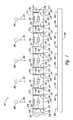
- FIG. 1is a schematic side cross-sectional view of a system 100 for testing a plurality of microelectronic imaging dies in accordance with an embodiment of the invention.
- the system 100is configured for testing of a plurality of imaging dies to verify and ensure that the imaging dies function according to specification.
- the system 100 illustrated in FIG. 1includes a microfeature workpiece 200 .
- the microfeature workpiece 200includes a substrate 210 having a front side 212 , a backside 214 , and a plurality of imaging dies 220 formed on and/or in the substrate 210 .
- the individual imaging dies 220can include an image sensor 240 , an integrated circuit 222 coupled to the image sensor 240 , and external contacts 230 electrically coupled to the integrated circuit 222 .
- the image sensors 240can be CMOS image sensors or CCD image sensors for capturing pictures or other images in the visible spectrum, but in other embodiments the image sensors 240 can detect radiation in other spectrums (e.g., IR or UV ranges).
- the image sensors 240are typically located at the front side 212 of the substrate 210 .
- the external contacts 230 shown in FIG. 1provide a small array of ball-pads within the footprint of each imaging die 220 .
- Each external contact 230can include a terminal 234 (e.g., a bond-pad), an external contact pad 236 (e.g., a ball-pad), and an interconnect 238 coupling the terminal 234 to the contact pad 236 .
- a solder ball 237is attached to each contact pad 236 to provide an external connection to other electronic devices (e.g., probe cards) on the backside 214 of the substrate 210 .
- the solder balls 237may be omitted.
- the terminals 234are on the front side 212 of the substrate 210
- the contact pads 236are on the backside 214 of the substrate 210
- the interconnects 238are through-wafer interconnects that extend completely through the substrate 210 to couple the terminals 234 to the contact pads 236 and corresponding solder balls 237 .
- the imaging dies 220may not include the terminals 234 on the front side 212 of the substrate 210 such that the integrated circuit 222 is coupled directly to the contact pads 236 on the backside 214 of the substrate 210 by through-wafer interconnects that extend through only a portion of the substrate 210 , or the terminals 234 can be within the substrate 210 .
- the system 100further includes a probe card 290 positioned proximate the backside 214 of the substrate 210 .
- the term “probe card”may encompass a variety of architectures, including both rigid structures and flexible structures and including probe assemblies adapted for testing single microelectronic components and those adapted for testing multiple devices simultaneously, such as the system 100 illustrated in FIG. 1 .
- the probe card 290 in the illustrated embodimentcan be formed according to the methods disclosed in U.S. patent application Ser. No. 10/230,653 (Perkins Coie Docket No. 108298684US), entitled “Probe Card, e.g., For Testing Microelectronic Components, and Methods for Making Same,” filed on Aug. 29, 2002, and herein incorporated by reference in its entirety.
- the probe card 290includes a plurality of pins 292 positioned to contact corresponding contact pads 236 and/or solder balls 237 on the individual dies 220 .
- the pins 292are in electrical communication with corresponding contact pads 236 and adapted to deliver and/or receive test signals (including source voltage, ground, etc.) to one more of the components being tested (e.g., image sensors 240 ).
- the pins 292are typically either a length of wire or a spring-biased mechanism (e.g., pogo pins).
- the pins 292can be arranged on the probe card 290 in an array corresponding to an array of the contact pads 236 and/or solder balls 237 on the backside 214 of the substrate 210 .
- the system 100 illustrated in FIG. 1further includes a plurality of light sources 280 positioned above the front side 212 of the substrate 210 and configured to provide light 282 to the image sensors 240 on the imaging dies 220 .
- light 282impinges on the individual image sensors 240 to test the functionality of the image sensors 240 and to ensure that the image sensors 240 function according to specification.
- the light 282 from the light sources 280is visible light.
- the image sensors 240can be configured to detect radiation in other spectrums (e.g., IR or UV ranges).
- the light sources 280can be radiation sources configured to produce IR- and/or UV-range radiation for testing the image sensors 240 .
- the external contacts 230provide arrays of contact pads 236 on the backside 214 of the substrate 210 .
- Each array of contact pads 236is operatively coupled to a corresponding image sensor 240 .
- the contact pads 236can be located on the backside 214 of the substrate 210 because the interconnects 238 are through-wafer interconnects that extend to the backside 214 of a substrate 210 .
- the backside arrays of contact pads 236allow the imaging units 240 to be operably coupled to the probe card 290 on the backside 214 of the substrate 210 .
- the probe card 290does not interfere with the image sensors 240 on the front side 212 of the substrate 210 during illumination and testing.
- this featureallows a plurality of imaging dies 220 to be tested simultaneously without interference from neighboring probe cards 290 and/or pins 292 . Further, the testing process can be more accurate because the image sensors 240 on the dies 220 can be fully illuminated without shadows or reflection from the probe card 290 and/or the pins 292 .
- Another feature of the illustrated system 100is that by testing from the backside 214 of the substrate 210 , potential contamination to the image sensors 240 on the front side 212 of the substrate 210 is mitigated or even eliminated.
- the image sensors 240are very susceptible to damage from contamination because, as noted above, a particle as small as ten microns can effectively ruin an image sensor.
- the image sensors 240can be covered before testing from the backside contact pads 236 to provide complete protection of the image sensors 240 .
- FIGS. 2-4illustrate several alternative embodiments of systems for testing microelectronic imaging dies.
- many of the featuresmay be the same as those discussed above in connection with the system 100 in FIG. 1 . Accordingly, like reference numbers are used to refer to like components in FIG. 1 and in FIGS. 2-4 .
- FIG. 2is a schematic side cross-sectional view of a system 120 for testing a plurality of microelectronic imaging dies in accordance with another embodiment of the invention.
- the system 120includes the microfeature workpiece 200 , the probe card 290 , and the light sources 280 described above with respect to FIG. 1 .
- the primary difference between the system 120 shown in FIG. 2 and the system 100 shown in FIG. 1is that the orientation of the microfeature workpiece 200 is inverted in the system 120 . More specifically, the front side 214 of the substrate 210 in this embodiment is oriented in a generally downward direction, as opposed to the generally upward orientation of the front side 214 of the substrate 210 in the system 100 .
- the probe card 290 and the light sources 280 in the illustrated embodimentare rearranged accordingly.
- One feature of this embodimentis that potential contamination of the image sensors 240 is further mitigated. Because the image sensors 240 on the front side 214 of the substrate 210 are oriented in a generally downward direction, debris is less likely to accumulate on the front side 214 of the substrate 210 and/or the image sensors 240 compared to the face-up orientation shown in FIG. 1 . Accordingly, the inverted orientation of the system 120 in the illustrated embodiment can enhance the protection of the image sensors 240 during testing.
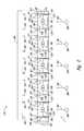
- FIG. 3is a schematic side cross-sectional view of a system 130 for testing a plurality of microelectronic imaging dies in accordance with another embodiment of the invention.
- the system 130includes a microfeature workpiece 300 and a probe card 390 generally similar to the components described above with respect to FIG. 1 .
- the microfeature workpiece 300includes a substrate 310 having a front side 312 , a backside 314 , and a plurality of imaging dies 320 formed on and/or in the substrate 310 .
- the individual imaging dies 320can include an image sensor 340 , an integrated circuit 322 electrically coupled to the image sensor 340 , and external contacts 330 electrically coupled to the integrated circuit 322 .
- the external contacts 330 shown in FIG. 3can be generally similar to the external contacts 230 described above with respect to FIG. 1 .
- Each external contact 330can include a terminal 334 (e.g., a bond-pad) at the front side 312 of the substrate 310 and an interconnect 338 in contact with the terminal 334 and extending through the substrate 310 .
- the workpiece 300differs from the workpiece 200 shown in FIG. 1 in that the external contacts on the backside 314 of the substrate 310 are of such a fine pitch that a redistribution assembly 370 is formed on the substrate 310 .
- the redistribution assembly 370includes a dielectric layer 372 , a plurality of ball-pads 336 at a backside 374 of the redistribution assembly 370 , and a plurality of traces 339 electrically coupling the ball-pads 336 to corresponding interconnects 338 . Accordingly, the ball-pads 336 provide an external connection to other electronic devices (e.g., probe cards). In another aspect of this embodiment, a solder ball (not shown) or other conductive element can be attached to each ball-pad 336 .
- the probe card 390has a plurality of pins 392 positioned at the backside 314 of the substrate 310 .
- the probe card 390differs from the probe card 290 shown in FIG. 1 in that the arrangement of the pins 392 on the probe card 390 is different.
- the pins 392can be arranged in an array corresponding to the ball-pads 336 on the redistribution assembly 370 .
- the system 130can further include the light sources 280 positioned above the front side 312 of the substrate 310 and configured to provide light 282 to the image sensors 340 on corresponding imaging dies 320 .
- the redistribution assembly 370provides arrays of ball-pads 336 that are spaced farther apart and have more surface area than the contact pads 236 shown in FIG. 1 . This feature is particularly important when positioning and attaching the pins 392 of the probe card 390 to ball-pads arranged in the high-density, fine pitch arrays that are common in high-performance imagers.
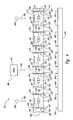
- FIG. 4is a schematic side cross-sectional view of a system 140 in accordance with another embodiment of the invention.
- the system 140can include the microfeature workpiece 200 and the probe card 290 described above in FIG. 1 .
- the system 140differs from the system 100 described above with respect to FIG. 1 in that the system 140 further includes a repair apparatus 480 to fuse repair electrical connections on the substrate 210 .
- the repair apparatus 480 in the illustrated embodimentincludes a laser 481 (shown schematically) that directs laser light 482 onto an antifuse 484 at the front side 212 of the substrate 210 .
- the laser light 482irradiates the antifuse 484 on the substrate 210 , thus reflowing the antifuse 484 and restoring the electrical connection to a failed connection on the dies 220 .
- the repair apparatus 480can have other configurations and/or irradiate the antifuse 484 in a different manner.
- One feature of the illustrated embodimentis that the fuse repair process can take place at one location on the front side 212 of the substrate 210 , while testing of the imaging dies 220 is taking place at another location on the front side 212 of the substrate 210 . Accordingly, the simultaneous repair/testing processes can result in faster throughput and lower manufacturing costs.
- FIGS. 5-7illustrate systems for testing microfeature devices in accordance with additional embodiments of the invention.
- FIG. 5is a schematic side cross-sectional view of a system 150 including a microfeature workpiece 500 and two probe cards 590 , 595 configured for testing microfeature devices 515 on the workpiece 500 .
- the system 150differs from the system 100 shown above in FIG. 1 in that the microfeature devices 515 on the workpiece 500 do not include image sensors.
- the microfeature workpiece 500 in the illustrated embodimentincludes a substrate 510 having a front side 512 , a backside 514 , and a plurality of microfeature devices 515 formed on and/or in the substrate 510 .
- the individual microfeature devices 515include a microelectronic die 520 having an integrated circuit 522 and a plurality of external contacts 530 electrically coupled to the integrated circuit 522 .
- the external contacts 530can be generally similar to the external contacts 230 described above with respect to FIG. 1 .
- Each external contact 530can include a terminal 534 (e.g., a bond-pad), an external contact pad 536 (e.g., a ball-pad), and an interconnect 538 coupling the terminal 534 to the contact pad 536 .
- the terminals 534are on the front side 512 of the substrate 510
- the contact pads 536are on the backside 514 of the substrate 510
- the interconnects 538are through-wafer interconnects that extend completely through the substrate 510 to couple the terminals 534 to corresponding contact pads 536 .
- the individual dies 520include some terminals 534 (e.g., terminals 534 a ) at the front side 512 of the substrate 510 that are not in contact with interconnects 538 extending through the substrate 510 .
- terminals 534 amust be tested from the front side 512 of the substrate 510 .
- the system 150includes a first probe card 590 at the backside 514 of the substrate 510 and a second probe card 595 at the front side 512 of the substrate 510 .
- the first probe card 590includes a plurality of pins 592 positioned to contact corresponding contact pads 536 on the backside 514 of the substrate 510
- the second probe card 595includes a plurality of pins 597 positioned to contact terminals 534 a on the front side 512 of the substrate 510
- the pins 592 , 597are in electrical communication with the dies 520 and adapted to deliver and/or receive test power (including test signals) to one more of the components of the dies 520 .
- the pins 592 , 597can be arranged on the first and second probe cards 590 , 595 in arrays corresponding to the arrays of corresponding contact pads 536 and terminals 534 , 534 a on the substrate 510 .
- One feature of the embodiment illustrated in FIG. 5is that the use of multiple probe cards provides for simultaneous testing of both terminals 534 coupled to interconnects 538 and terminals 534 a not coupled to interconnects 538 . Accordingly, this feature provides flexibility in the testing process in that microelectronic dies having terminals with and without connections to interconnects can be tested quickly and without additional steps being required in the testing process. Furthermore, this feature minimizes the amount of time it takes to test a workpiece since testing can occur from both the front side and the backside of the substrate.
- FIG. 6is a schematic side cross-sectional view of a system 160 in accordance with another embodiment of the invention.
- the system 160can include a microfeature workpiece 600 with a substrate 610 having a front side 612 , a backside 614 , and a plurality of microfeature devices 615 formed on and/or in the substrate 610 .
- the microfeature devices 615can be generally similar to the devices 515 described above with respect to FIG. 5 .
- the individual microfeature devices 615have a microelectronic die 620 including an integrated circuit 622 and a plurality of external contacts 630 electrically coupled to the integrated circuit 622 .
- Each external contact 630can include a terminal 634 (e.g., a bond-pad) on the front side 612 of the substrate 610 , an external contact pad 636 (e.g., a ball-pad) on the backside 614 of the substrate 610 , and a through-wafer interconnect 638 extending completely through the substrate 610 coupling the terminals 634 to corresponding contact pads 636 .
- a terminal 634e.g., a bond-pad
- an external contact pad 636e.g., a ball-pad
- the system 160further includes a first probe card 690 having a plurality of pins 692 positioned proximate the backside 614 of the substrate 610 and a second probe card 695 having a plurality of pins 697 positioned proximate the front side 612 of the substrate 610 .
- the pins 692 , 697can be arranged on the first and second probe cards 690 , 695 in arrays corresponding to the arrays of contact pads 636 and terminals 634 on the substrate 610 .
- the external contacts 630 in the illustrated embodimentdiffer from the external contacts 530 shown in FIG. 5 in that density of the terminals 634 on the front side 612 of the substrate 610 is so great (e.g., having approximately zero pitch) that the terminals 634 cannot all be tested from one side of the substrate 610 . Accordingly, the terminals 634 must be tested by probing alternate front side terminals 634 and backside contact pads 636 .
- pins 692 a and 692 c on the first probe card 690are in electrical communication with contact pads 636 a and 636 c (and accordingly terminals 634 a and 634 c via interconnects 638 ).
- Terminals 634 b and 634 dare not in electrical communication with probe card 690 . Rather, terminals 634 b and 634 d (and accordingly contact pads 636 b and 636 d via interconnects 638 ) are contacted by pins 697 b and 697 d on the second probe card 695 .
- a plurality of dies 620 having fine-pitch arrayscan be tested simultaneously by probing alternating terminals 634 and contact pads 636 on both the front side 612 and the backside 614 of the substrate 610 , even though the arrays of terminals 634 and/or contact pads 636 on the individual dies 620 are too dense for the probe cards 690 , 695 .
- construction of the probe cards 690 , 695can be simplified because each probe card will not have to be configured to test the entire high-density array. Rather, individual probe cards will only require enough pins to test alternate electrical contacts on corresponding sides of the substrate 610 .
- FIG. 7illustrates a system 170 that is a combination of the microfeature workpiece 200 , probe card 290 , and light sources 280 shown in FIG. 1 with the microfeature workpiece 500 from FIG. 5 .
- the imaging dies 220 and microelectronic dies 520can be tested together as shown. Accordingly, the invention is not limited except as by the appended claims.
Landscapes
- Physics & Mathematics (AREA)
- General Physics & Mathematics (AREA)
- Engineering & Computer Science (AREA)
- General Engineering & Computer Science (AREA)
- Optics & Photonics (AREA)
- Testing Or Measuring Of Semiconductors Or The Like (AREA)
Abstract
Description
- The present invention is related to systems and methods for testing microelectronic imagers and microfeature devices.
- The microelectronics industry is highly competitive and microelectronics manufacturers are very sensitive to quality and cost considerations. Most microelectronics manufacturers require that suppliers of microelectronic components test the performance of each microelectronic component before shipment to minimize the manufacturer's product losses. For example, microelectronic imagers are commonly tested by establishing temporary electrical connections between a test system and electrical contacts on each microelectronic imaging die while simultaneously exposing an image sensor on the device to light.
- One way of establishing a temporary electrical connection between the test system and the contacts on a microelectronic component employs a probe card carrying a plurality of probe pins. The probe pins are typically either a length of wire (e.g., cantilevered wire probes) or a relatively complex spring-biased mechanism (e.g., pogo pins). The probe pins are connected to the probe card and arranged in a predetermined array for use with a specific microelectronic component configuration. For example, when testing a microelectronic imager with a conventional probe card (whether it be a cantilevered wire probe card, a pogo pin probe card, or another design), the probe card is positioned proximate to the front side of the imaging die to be tested. The probe card and the imaging die are aligned with each other in an effort to precisely align each of the probe pins of the probe card with a corresponding electrical contact of the front side of the imaging die.
- One problem with testing imaging dies at the wafer level is that it is difficult to expose an image sensor to light while simultaneously aligning the probe pins or the body of the probe card with the corresponding electrical contacts on the front side of the imaging die. For example, because the probe card is positioned over the image sensor to contact the front side bond-pads on the die, the probe card must have a plurality of holes or apertures through which light can pass. This limits wafer-level testing methods because the physical constraints of probe card structures and the limited testing area available on the wafer. Further, the probe card and/or probe pins positioned proximate (but not over) the image sensor also interfere with the light directed to the image sensor (e.g., shadowing, reflections). These limitations result in the ability to test only a fraction of the imaging dies on a wafer of imaging dies as compared to the number of other types of dies that can be tested in non-imaging applications (e.g., memory, processors, etc.). For example, only four CMOS imaging dies can be tested simultaneously on a wafer compared to 128 DRAM dies using the same equipment. Accordingly, there is a need to improve the efficiency and throughput for testing imaging dies.
- Another problem with conventional probe card testing methods is that the testing process can introduce moisture and/or other contaminants to the image sensors. For example, conventional probe cards and/or probe pins are positioned over the image sensors to contact the bond-pads on the front side of the dies. Accordingly, tiny particles generated during the testing process or otherwise on the probe pins can fall onto the image sensors. This can cause a malfunction or failure because a particle as small as ten microns can effectively ruin an image sensor. Accordingly, there is a further need to improve the testing of imaging dies.
FIG. 1 is a schematic side cross-sectional view of a system for testing a plurality of microelectronic imaging dies in accordance with one embodiment of the invention.FIG. 2 is a schematic side cross-sectional view of a system for testing a plurality of microelectronic imaging dies in accordance with another embodiment of the invention.FIG. 3 is a schematic side cross-sectional view of a system for testing a plurality of microelectronic imaging dies in accordance with another embodiment of the invention.FIG. 4 is a schematic side cross-sectional view of a system for testing a plurality of microelectronic imaging dies while simultaneously repairing fuses on a workpiece in accordance with one embodiment of the invention.FIG. 5 is a schematic side cross-sectional view of a system for testing a plurality of microfeature devices in accordance with one embodiment of the invention.FIG. 6 is a schematic side cross-sectional view of a system for testing a plurality of microfeature devices in accordance with one embodiment of the invention.FIG. 7 is a schematic side cross-sectional view of a system for testing a plurality of microelectronic imaging dies along with a plurality of microfeature devices in accordance with one embodiment of the invention.- A. Overview
- The present invention is directed toward systems and methods for testing microelectronic imagers and microfeature devices. The term “microfeature device” is used throughout to include microelectronic devices, micromechanical devices, data storage elements, read/write components, and other articles of manufacture. For example, microfeature devices include SIMM, DRAM, flash-memory, ASICS, processors, flip chips, ball-grid array chips, and other types of electronic devices or components. Several specific details of the invention are set forth in the following description and in
FIGS. 1-7 to provide a thorough understanding of certain embodiments of the invention. One skilled in the art, however, will understand that the present invention may have additional embodiments or that embodiments of the invention may be practiced without several of the specific features described below. - One aspect of the invention is directed to methods for testing microfeature devices and microelectronic imaging dies from a backside of a workpiece. In one embodiment, a method includes providing a microfeature workpiece including a substrate having a front side, a backside, and a plurality of microelectronic dies. The individual dies include an integrated circuit and a plurality of contact pads at the backside of the substrate operatively coupled to the integrated circuit. The method further includes contacting individual contact pads with corresponding pins of a probe card and testing the dies.
- Another embodiment of a method for testing microfeature devices in accordance with the invention includes testing microelectronic imaging dies. The method comprises providing a microfeature workpiece including a substrate having a front side, a backside, and a plurality of microelectronic imaging dies. The individual dies include an image sensor, an integrated circuit electrically coupled to the image sensor, a plurality of contact pads at the backside of the substrate, and through-wafer interconnects extending at least partially through the substrate and electrically coupling corresponding contact pads to the integrated circuit. The method includes contacting individual contact pads at the backside of the substrate with corresponding pins of a probe card. The method then includes illuminating the image sensors while testing the dies.
- Another embodiment of a method for testing microfeature devices in accordance with the invention includes testing the microfeature devices from both the front side and backside. The method comprises providing a microfeature workpiece including a substrate having a plurality of microelectronic dies. The individual dies have an integrated circuit, a plurality of terminals at the front side of the substrate operatively coupled to the integrated circuit, a plurality of contact pads at the backside of the substrate operatively coupled to the integrated circuit, and through-wafer interconnects extending through the substrate and electrically coupling the terminals to corresponding contact pads. The method further includes contacting individual terminals with corresponding pins of a first probe card while contacting individual contact pads with corresponding pins of a second probe card. The contact pads being contacted by the second probe card are not in electrical contact with the terminals being contacted by the first probe card. The method then includes testing the dies.
- Another aspect of this invention is directed toward systems for testing microfeature devices and microelectronic imaging dies. One embodiment of a system in accordance with the invention comprises a microfeature workpiece including a substrate having a plurality of microelectronic dies. The individual dies include an integrated circuit and through-wafer interconnects extending through at least a portion of the substrate and operatively coupled to the integrated circuit. The dies further include a plurality of contact pads at the backside of the substrate and operatively coupled to the integrated circuit. The system also includes a probe card having a plurality of pins positioned to contact corresponding contact pads and test the dies.
- B. Embodiments of Methods for Testing Microelectronic Imaging Dies
FIG. 1 is a schematic side cross-sectional view of asystem 100 for testing a plurality of microelectronic imaging dies in accordance with an embodiment of the invention. Thesystem 100 is configured for testing of a plurality of imaging dies to verify and ensure that the imaging dies function according to specification.- The
system 100 illustrated inFIG. 1 includes amicrofeature workpiece 200. Themicrofeature workpiece 200 includes asubstrate 210 having afront side 212, abackside 214, and a plurality of imaging dies220 formed on and/or in thesubstrate 210. Theindividual imaging dies 220 can include animage sensor 240, an integratedcircuit 222 coupled to theimage sensor 240, andexternal contacts 230 electrically coupled to the integratedcircuit 222. Theimage sensors 240 can be CMOS image sensors or CCD image sensors for capturing pictures or other images in the visible spectrum, but in other embodiments theimage sensors 240 can detect radiation in other spectrums (e.g., IR or UV ranges). Theimage sensors 240 are typically located at thefront side 212 of thesubstrate 210. - The
external contacts 230 shown inFIG. 1 provide a small array of ball-pads within the footprint of each imaging die220. Eachexternal contact 230, for example, can include a terminal234 (e.g., a bond-pad), an external contact pad236 (e.g., a ball-pad), and aninterconnect 238 coupling the terminal234 to thecontact pad 236. In another aspect of this embodiment, asolder ball 237 is attached to eachcontact pad 236 to provide an external connection to other electronic devices (e.g., probe cards) on thebackside 214 of thesubstrate 210. In other embodiments, thesolder balls 237 may be omitted. - In the embodiment shown in
FIG. 1 , theterminals 234 are on thefront side 212 of thesubstrate 210, thecontact pads 236 are on thebackside 214 of thesubstrate 210, and theinterconnects 238 are through-wafer interconnects that extend completely through thesubstrate 210 to couple theterminals 234 to thecontact pads 236 andcorresponding solder balls 237. In other embodiments, however, the imaging dies220 may not include theterminals 234 on thefront side 212 of thesubstrate 210 such that theintegrated circuit 222 is coupled directly to thecontact pads 236 on thebackside 214 of thesubstrate 210 by through-wafer interconnects that extend through only a portion of thesubstrate 210, or theterminals 234 can be within thesubstrate 210. - The
system 100 further includes aprobe card 290 positioned proximate thebackside 214 of thesubstrate 210. In this disclosure, the term “probe card” may encompass a variety of architectures, including both rigid structures and flexible structures and including probe assemblies adapted for testing single microelectronic components and those adapted for testing multiple devices simultaneously, such as thesystem 100 illustrated inFIG. 1 . Theprobe card 290 in the illustrated embodiment can be formed according to the methods disclosed in U.S. patent application Ser. No. 10/230,653 (Perkins Coie Docket No. 108298684US), entitled “Probe Card, e.g., For Testing Microelectronic Components, and Methods for Making Same,” filed on Aug. 29, 2002, and herein incorporated by reference in its entirety. - The
probe card 290 includes a plurality ofpins 292 positioned to contactcorresponding contact pads 236 and/orsolder balls 237 on the individual dies220. During testing, thepins 292 are in electrical communication withcorresponding contact pads 236 and adapted to deliver and/or receive test signals (including source voltage, ground, etc.) to one more of the components being tested (e.g., image sensors240). Thepins 292 are typically either a length of wire or a spring-biased mechanism (e.g., pogo pins). Thepins 292 can be arranged on theprobe card 290 in an array corresponding to an array of thecontact pads 236 and/orsolder balls 237 on thebackside 214 of thesubstrate 210. - The
system 100 illustrated inFIG. 1 further includes a plurality oflight sources 280 positioned above thefront side 212 of thesubstrate 210 and configured to provide light282 to theimage sensors 240 on the imaging dies220. During testing, light282 impinges on theindividual image sensors 240 to test the functionality of theimage sensors 240 and to ensure that theimage sensors 240 function according to specification. In the illustrated embodiment, the light282 from thelight sources 280 is visible light. In further embodiments, however, theimage sensors 240 can be configured to detect radiation in other spectrums (e.g., IR or UV ranges). Accordingly, thelight sources 280 can be radiation sources configured to produce IR- and/or UV-range radiation for testing theimage sensors 240. - One feature of the illustrated
system 100 is that theexternal contacts 230 provide arrays ofcontact pads 236 on thebackside 214 of thesubstrate 210. Each array ofcontact pads 236 is operatively coupled to acorresponding image sensor 240. More specifically, thecontact pads 236 can be located on thebackside 214 of thesubstrate 210 because theinterconnects 238 are through-wafer interconnects that extend to thebackside 214 of asubstrate 210. Accordingly, the backside arrays ofcontact pads 236 allow theimaging units 240 to be operably coupled to theprobe card 290 on thebackside 214 of thesubstrate 210. As such, theprobe card 290 does not interfere with theimage sensors 240 on thefront side 212 of thesubstrate 210 during illumination and testing. Moreover, this feature allows a plurality of imaging dies220 to be tested simultaneously without interference from neighboringprobe cards 290 and/or pins292. Further, the testing process can be more accurate because theimage sensors 240 on the dies220 can be fully illuminated without shadows or reflection from theprobe card 290 and/or thepins 292. - Another feature of the illustrated
system 100 is that by testing from thebackside 214 of thesubstrate 210, potential contamination to theimage sensors 240 on thefront side 212 of thesubstrate 210 is mitigated or even eliminated. Theimage sensors 240 are very susceptible to damage from contamination because, as noted above, a particle as small as ten microns can effectively ruin an image sensor. By testing from thebackside 214 of thesubstrate 210, particles cannot fall from theprobe card 290 and/or pins292 to theimage sensors 240. Moreover, theimage sensors 240 can be covered before testing from thebackside contact pads 236 to provide complete protection of theimage sensors 240. - C. Additional Embodiments of Methods for Testing Microelectronic Imaging Dies
FIGS. 2-4 illustrate several alternative embodiments of systems for testing microelectronic imaging dies. In each ofFIGS. 2-4 , many of the features may be the same as those discussed above in connection with thesystem 100 inFIG. 1 . Accordingly, like reference numbers are used to refer to like components inFIG. 1 and inFIGS. 2-4 .FIG. 2 is a schematic side cross-sectional view of asystem 120 for testing a plurality of microelectronic imaging dies in accordance with another embodiment of the invention. Thesystem 120 includes themicrofeature workpiece 200, theprobe card 290, and thelight sources 280 described above with respect toFIG. 1 . The primary difference between thesystem 120 shown inFIG. 2 and thesystem 100 shown inFIG. 1 is that the orientation of themicrofeature workpiece 200 is inverted in thesystem 120. More specifically, thefront side 214 of thesubstrate 210 in this embodiment is oriented in a generally downward direction, as opposed to the generally upward orientation of thefront side 214 of thesubstrate 210 in thesystem 100. Theprobe card 290 and thelight sources 280 in the illustrated embodiment are rearranged accordingly. One feature of this embodiment is that potential contamination of theimage sensors 240 is further mitigated. Because theimage sensors 240 on thefront side 214 of thesubstrate 210 are oriented in a generally downward direction, debris is less likely to accumulate on thefront side 214 of thesubstrate 210 and/or theimage sensors 240 compared to the face-up orientation shown inFIG. 1 . Accordingly, the inverted orientation of thesystem 120 in the illustrated embodiment can enhance the protection of theimage sensors 240 during testing.FIG. 3 is a schematic side cross-sectional view of asystem 130 for testing a plurality of microelectronic imaging dies in accordance with another embodiment of the invention. In one aspect of this embodiment, thesystem 130 includes amicrofeature workpiece 300 and aprobe card 390 generally similar to the components described above with respect toFIG. 1 . Themicrofeature workpiece 300 includes asubstrate 310 having afront side 312, abackside 314, and a plurality of imaging dies320 formed on and/or in thesubstrate 310. The individual imaging dies320 can include animage sensor 340, anintegrated circuit 322 electrically coupled to theimage sensor 340, andexternal contacts 330 electrically coupled to theintegrated circuit 322.- The
external contacts 330 shown inFIG. 3 can be generally similar to theexternal contacts 230 described above with respect toFIG. 1 . Eachexternal contact 330, for example, can include a terminal334 (e.g., a bond-pad) at thefront side 312 of thesubstrate 310 and aninterconnect 338 in contact with the terminal334 and extending through thesubstrate 310. Theworkpiece 300, however, differs from theworkpiece 200 shown inFIG. 1 in that the external contacts on thebackside 314 of thesubstrate 310 are of such a fine pitch that aredistribution assembly 370 is formed on thesubstrate 310. Theredistribution assembly 370 includes adielectric layer 372, a plurality of ball-pads 336 at abackside 374 of theredistribution assembly 370, and a plurality oftraces 339 electrically coupling the ball-pads 336 tocorresponding interconnects 338. Accordingly, the ball-pads 336 provide an external connection to other electronic devices (e.g., probe cards). In another aspect of this embodiment, a solder ball (not shown) or other conductive element can be attached to each ball-pad 336. - The
probe card 390 has a plurality ofpins 392 positioned at thebackside 314 of thesubstrate 310. Theprobe card 390 differs from theprobe card 290 shown inFIG. 1 in that the arrangement of thepins 392 on theprobe card 390 is different. Thepins 392 can be arranged in an array corresponding to the ball-pads 336 on theredistribution assembly 370. In another aspect of the embodiment illustrated inFIG. 3 , thesystem 130 can further include thelight sources 280 positioned above thefront side 312 of thesubstrate 310 and configured to provide light282 to theimage sensors 340 on corresponding imaging dies320. - One feature of the illustrated embodiment is that the
redistribution assembly 370 provides arrays of ball-pads 336 that are spaced farther apart and have more surface area than thecontact pads 236 shown inFIG. 1 . This feature is particularly important when positioning and attaching thepins 392 of theprobe card 390 to ball-pads arranged in the high-density, fine pitch arrays that are common in high-performance imagers. FIG. 4 is a schematic side cross-sectional view of asystem 140 in accordance with another embodiment of the invention. In one aspect of this embodiment, thesystem 140 can include themicrofeature workpiece 200 and theprobe card 290 described above inFIG. 1 . Thesystem 140 differs from thesystem 100 described above with respect toFIG. 1 in that thesystem 140 further includes arepair apparatus 480 to fuse repair electrical connections on thesubstrate 210. Therepair apparatus 480 in the illustrated embodiment includes a laser481 (shown schematically) that directslaser light 482 onto anantifuse 484 at thefront side 212 of thesubstrate 210. Thelaser light 482 irradiates theantifuse 484 on thesubstrate 210, thus reflowing theantifuse 484 and restoring the electrical connection to a failed connection on the dies220. In other embodiments, therepair apparatus 480 can have other configurations and/or irradiate theantifuse 484 in a different manner. One feature of the illustrated embodiment is that the fuse repair process can take place at one location on thefront side 212 of thesubstrate 210, while testing of the imaging dies220 is taking place at another location on thefront side 212 of thesubstrate 210. Accordingly, the simultaneous repair/testing processes can result in faster throughput and lower manufacturing costs.- D. Additional Embodiments of Methods for Testing Microfeature Devices
FIGS. 5-7 illustrate systems for testing microfeature devices in accordance with additional embodiments of the invention. For example,FIG. 5 is a schematic side cross-sectional view of asystem 150 including amicrofeature workpiece 500 and twoprobe cards microfeature devices 515 on theworkpiece 500. Thesystem 150 differs from thesystem 100 shown above inFIG. 1 in that themicrofeature devices 515 on theworkpiece 500 do not include image sensors.- The
microfeature workpiece 500 in the illustrated embodiment includes asubstrate 510 having afront side 512, abackside 514, and a plurality ofmicrofeature devices 515 formed on and/or in thesubstrate 510. Theindividual microfeature devices 515 include amicroelectronic die 520 having anintegrated circuit 522 and a plurality ofexternal contacts 530 electrically coupled to theintegrated circuit 522. - The
external contacts 530 can be generally similar to theexternal contacts 230 described above with respect toFIG. 1 . Eachexternal contact 530, for example, can include a terminal534 (e.g., a bond-pad), an external contact pad536 (e.g., a ball-pad), and aninterconnect 538 coupling the terminal534 to thecontact pad 536. In the embodiment shown inFIG. 5 , theterminals 534 are on thefront side 512 of thesubstrate 510, thecontact pads 536 are on thebackside 514 of thesubstrate 510, and theinterconnects 538 are through-wafer interconnects that extend completely through thesubstrate 510 to couple theterminals 534 tocorresponding contact pads 536. - In another aspect of this embodiment, the individual dies520 include some terminals534 (e.g.,
terminals 534a) at thefront side 512 of thesubstrate 510 that are not in contact withinterconnects 538 extending through thesubstrate 510. As such,terminals 534amust be tested from thefront side 512 of thesubstrate 510. Accordingly, thesystem 150 includes afirst probe card 590 at thebackside 514 of thesubstrate 510 and asecond probe card 595 at thefront side 512 of thesubstrate 510. Thefirst probe card 590 includes a plurality ofpins 592 positioned to contactcorresponding contact pads 536 on thebackside 514 of thesubstrate 510, while thesecond probe card 595 includes a plurality ofpins 597 positioned to contactterminals 534aon thefront side 512 of thesubstrate 510. During testing, thepins pins second probe cards corresponding contact pads 536 andterminals substrate 510. - One feature of the embodiment illustrated in
FIG. 5 is that the use of multiple probe cards provides for simultaneous testing of bothterminals 534 coupled tointerconnects 538 andterminals 534anot coupled to interconnects538. Accordingly, this feature provides flexibility in the testing process in that microelectronic dies having terminals with and without connections to interconnects can be tested quickly and without additional steps being required in the testing process. Furthermore, this feature minimizes the amount of time it takes to test a workpiece since testing can occur from both the front side and the backside of the substrate. FIG. 6 is a schematic side cross-sectional view of asystem 160 in accordance with another embodiment of the invention. In the illustrated embodiment, thesystem 160 can include amicrofeature workpiece 600 with asubstrate 610 having afront side 612, abackside 614, and a plurality ofmicrofeature devices 615 formed on and/or in thesubstrate 610. Themicrofeature devices 615 can be generally similar to thedevices 515 described above with respect toFIG. 5 . Theindividual microfeature devices 615 have amicroelectronic die 620 including anintegrated circuit 622 and a plurality ofexternal contacts 630 electrically coupled to theintegrated circuit 622. Eachexternal contact 630 can include a terminal634 (e.g., a bond-pad) on thefront side 612 of thesubstrate 610, an external contact pad636 (e.g., a ball-pad) on thebackside 614 of thesubstrate 610, and a through-wafer interconnect 638 extending completely through thesubstrate 610 coupling theterminals 634 tocorresponding contact pads 636.- The
system 160 further includes afirst probe card 690 having a plurality ofpins 692 positioned proximate thebackside 614 of thesubstrate 610 and asecond probe card 695 having a plurality ofpins 697 positioned proximate thefront side 612 of thesubstrate 610. Thepins second probe cards contact pads 636 andterminals 634 on thesubstrate 610. - The
external contacts 630 in the illustrated embodiment differ from theexternal contacts 530 shown inFIG. 5 in that density of theterminals 634 on thefront side 612 of thesubstrate 610 is so great (e.g., having approximately zero pitch) that theterminals 634 cannot all be tested from one side of thesubstrate 610. Accordingly, theterminals 634 must be tested by probing alternatefront side terminals 634 andbackside contact pads 636. - For example, pins692aand692con the
first probe card 690 are in electrical communication withcontact pads terminals Terminals probe card 690. Rather,terminals pads pins second probe card 695. Accordingly, a plurality of dies620 having fine-pitch arrays can be tested simultaneously by probing alternatingterminals 634 andcontact pads 636 on both thefront side 612 and thebackside 614 of thesubstrate 610, even though the arrays ofterminals 634 and/orcontact pads 636 on the individual dies620 are too dense for theprobe cards probe cards substrate 610. - From the foregoing, it will be appreciated that specific embodiments of the invention have been described herein for purposes of illustration, but that various modifications may be made without deviating from the spirit and scope of the invention. Furthermore, various aspects of any of the foregoing embodiments can be combined in different combinations.
FIG. 7 , for example, illustrates asystem 170 that is a combination of themicrofeature workpiece 200,probe card 290, andlight sources 280 shown inFIG. 1 with themicrofeature workpiece 500 fromFIG. 5 . The imaging dies220 and microelectronic dies520 can be tested together as shown. Accordingly, the invention is not limited except as by the appended claims.
Claims (47)
Priority Applications (2)
| Application Number | Priority Date | Filing Date | Title |
|---|---|---|---|
| US10/860,699US7148715B2 (en) | 2004-06-02 | 2004-06-02 | Systems and methods for testing microelectronic imagers and microfeature devices |
| US11/409,060US7385412B2 (en) | 2004-06-02 | 2006-04-24 | Systems and methods for testing microfeature devices |
Applications Claiming Priority (1)
| Application Number | Priority Date | Filing Date | Title |
|---|---|---|---|
| US10/860,699US7148715B2 (en) | 2004-06-02 | 2004-06-02 | Systems and methods for testing microelectronic imagers and microfeature devices |
Related Child Applications (1)
| Application Number | Title | Priority Date | Filing Date |
|---|---|---|---|
| US11/409,060DivisionUS7385412B2 (en) | 2004-06-02 | 2006-04-24 | Systems and methods for testing microfeature devices |
Publications (2)
| Publication Number | Publication Date |
|---|---|
| US20050270055A1true US20050270055A1 (en) | 2005-12-08 |
| US7148715B2 US7148715B2 (en) | 2006-12-12 |
Family
ID=35446989
Family Applications (2)
| Application Number | Title | Priority Date | Filing Date |
|---|---|---|---|
| US10/860,699Expired - LifetimeUS7148715B2 (en) | 2004-06-02 | 2004-06-02 | Systems and methods for testing microelectronic imagers and microfeature devices |
| US11/409,060Expired - LifetimeUS7385412B2 (en) | 2004-06-02 | 2006-04-24 | Systems and methods for testing microfeature devices |
Family Applications After (1)
| Application Number | Title | Priority Date | Filing Date |
|---|---|---|---|
| US11/409,060Expired - LifetimeUS7385412B2 (en) | 2004-06-02 | 2006-04-24 | Systems and methods for testing microfeature devices |
Country Status (1)
| Country | Link |
|---|---|
| US (2) | US7148715B2 (en) |
Cited By (16)
| Publication number | Priority date | Publication date | Assignee | Title |
|---|---|---|---|---|
| US20050275750A1 (en)* | 2004-06-09 | 2005-12-15 | Salman Akram | Wafer-level packaged microelectronic imagers and processes for wafer-level packaging |
| WO2007027880A2 (en) | 2005-09-01 | 2007-03-08 | Micron Technology, Inc. | Microelectronic imaging units and methods of manufacturing microelectronic imaging units at the wafer level |
| US20070057384A1 (en)* | 2005-09-14 | 2007-03-15 | Alam Syed M | Semiconductor stacked die/wafer configuration and packaging and method thereof |
| US20070117253A1 (en)* | 2005-11-23 | 2007-05-24 | Taiwan Semiconductor Manufacturing Company, Ltd. | Method for providing metal extension in backside illuminated sensor for wafer level testing |
| US20070144841A1 (en)* | 2001-11-21 | 2007-06-28 | Chong Fu C | Miniaturized Contact Spring |
| WO2007131194A3 (en)* | 2006-05-05 | 2008-04-17 | Nanonexus Inc | Apparatus and methods for processing, testing, and packaging of semiconductor ics and image sensors |
| US20080246500A1 (en)* | 2000-05-23 | 2008-10-09 | Fu Chiung Chong | High density interconnect system having rapid fabrication cycle |
| US20080297185A1 (en)* | 2007-05-31 | 2008-12-04 | Samsung Electronics Co., Ltd. | Multi probe card unit, probe test device including the multi probe card unit, and methods of fabricating and using the same |
| US20080308946A1 (en)* | 2007-06-15 | 2008-12-18 | Micron Technology, Inc. | Semiconductor assemblies, stacked semiconductor devices, and methods of manufacturing semiconductor assemblies and stacked semiconductor devices |
| US7621761B2 (en) | 2000-06-20 | 2009-11-24 | Nanonexus, Inc. | Systems for testing and packaging integrated circuits |
| US7772860B2 (en) | 1999-05-27 | 2010-08-10 | Nanonexus, Inc. | Massively parallel interface for electronic circuit |
| US7807505B2 (en)* | 2005-08-30 | 2010-10-05 | Micron Technology, Inc. | Methods for wafer-level packaging of microfeature devices and microfeature devices formed using such methods |
| US20120007256A1 (en)* | 2006-08-30 | 2012-01-12 | Micron Technology, Inc. | Redistribution layers for microfeature workpieces, and associated systems and methods |
| CN104350588A (en)* | 2012-04-09 | 2015-02-11 | 高级查询系统公司 | Translators coupleable to opposing surfaces of microelectronic substrates for testing, and associated systems and methods |
| CN112967945A (en)* | 2020-04-16 | 2021-06-15 | 重庆康佳光电技术研究院有限公司 | Micro light-emitting diode testing device, manufacturing method, system and testing method |
| CN115172312A (en)* | 2021-04-06 | 2022-10-11 | 格科微电子(上海)有限公司 | Wafer and chip testing method for semiconductor |
Families Citing this family (6)
| Publication number | Priority date | Publication date | Assignee | Title |
|---|---|---|---|---|
| CN1954202A (en)* | 2004-06-08 | 2007-04-25 | 株式会社爱德万测试 | Image sensor test device |
| KR100805834B1 (en)* | 2006-01-09 | 2008-02-21 | 삼성전자주식회사 | Apparatus for testing a light receiving element and method of the same |
| US20080218186A1 (en)* | 2007-03-07 | 2008-09-11 | Jeff Kooiman | Image sensing integrated circuit test apparatus and method |
| US7868630B2 (en)* | 2007-06-26 | 2011-01-11 | Micron Technology, Inc. | Integrated light conditioning devices on a probe card for testing imaging devices, and methods of fabricating same |
| US8754412B2 (en) | 2012-01-03 | 2014-06-17 | International Business Machines Corporation | Intra die variation monitor using through-silicon via |
| JP7005620B2 (en)* | 2016-12-09 | 2022-01-21 | フォームファクター, インコーポレイテッド | LED light source probe card technology for testing CMOS image scanning devices |
Citations (8)
| Publication number | Priority date | Publication date | Assignee | Title |
|---|---|---|---|---|
| US6143588A (en)* | 1997-09-09 | 2000-11-07 | Amkor Technology, Inc. | Method of making an integrated circuit package employing a transparent encapsulant |
| US6639418B2 (en)* | 2001-11-21 | 2003-10-28 | Taiwan Semiconductor Manufacturing Co., Ltd. | Microelectronic fabrication die electrical probe apparatus electrical test method providing enhanced microelectronic fabrication die electrical test accuracy and efficiency |
| US20040035917A1 (en)* | 2002-08-22 | 2004-02-26 | Michel Koopmans | Apparatus and method for depositing and reflowing solder paste on a microelectronic workpiece |
| US6734419B1 (en)* | 2001-06-28 | 2004-05-11 | Amkor Technology, Inc. | Method for forming an image sensor package with vision die in lens housing |
| US6881974B2 (en)* | 2002-08-29 | 2005-04-19 | Micron Technology, Inc. | Probe card for testing microelectronic components |
| US6885101B2 (en)* | 2002-08-29 | 2005-04-26 | Micron Technology, Inc. | Methods for wafer-level packaging of microelectronic devices and microelectronic devices formed by such methods |
| US6946325B2 (en)* | 2003-03-14 | 2005-09-20 | Micron Technology, Inc. | Methods for packaging microelectronic devices |
| US20050206401A1 (en)* | 2004-03-22 | 2005-09-22 | Caldwell John L | Test sockets, test systems, and methods for testing microfeature devices |
Family Cites Families (1)
| Publication number | Priority date | Publication date | Assignee | Title |
|---|---|---|---|---|
| US7115961B2 (en)* | 2004-08-24 | 2006-10-03 | Micron Technology, Inc. | Packaged microelectronic imaging devices and methods of packaging microelectronic imaging devices |
- 2004
- 2004-06-02USUS10/860,699patent/US7148715B2/ennot_activeExpired - Lifetime
- 2006
- 2006-04-24USUS11/409,060patent/US7385412B2/ennot_activeExpired - Lifetime
Patent Citations (9)
| Publication number | Priority date | Publication date | Assignee | Title |
|---|---|---|---|---|
| US6143588A (en)* | 1997-09-09 | 2000-11-07 | Amkor Technology, Inc. | Method of making an integrated circuit package employing a transparent encapsulant |
| US6734419B1 (en)* | 2001-06-28 | 2004-05-11 | Amkor Technology, Inc. | Method for forming an image sensor package with vision die in lens housing |
| US6639418B2 (en)* | 2001-11-21 | 2003-10-28 | Taiwan Semiconductor Manufacturing Co., Ltd. | Microelectronic fabrication die electrical probe apparatus electrical test method providing enhanced microelectronic fabrication die electrical test accuracy and efficiency |
| US20040035917A1 (en)* | 2002-08-22 | 2004-02-26 | Michel Koopmans | Apparatus and method for depositing and reflowing solder paste on a microelectronic workpiece |
| US6881974B2 (en)* | 2002-08-29 | 2005-04-19 | Micron Technology, Inc. | Probe card for testing microelectronic components |
| US6885101B2 (en)* | 2002-08-29 | 2005-04-26 | Micron Technology, Inc. | Methods for wafer-level packaging of microelectronic devices and microelectronic devices formed by such methods |
| US6946325B2 (en)* | 2003-03-14 | 2005-09-20 | Micron Technology, Inc. | Methods for packaging microelectronic devices |
| US20050206401A1 (en)* | 2004-03-22 | 2005-09-22 | Caldwell John L | Test sockets, test systems, and methods for testing microfeature devices |
| US20060197545A1 (en)* | 2004-03-22 | 2006-09-07 | Micron Technology, Inc. | Test sockets, test systems, and methods for testing microfeature devices |
Cited By (28)
| Publication number | Priority date | Publication date | Assignee | Title |
|---|---|---|---|---|
| US7772860B2 (en) | 1999-05-27 | 2010-08-10 | Nanonexus, Inc. | Massively parallel interface for electronic circuit |
| US7884634B2 (en) | 1999-05-27 | 2011-02-08 | Verigy (Singapore) Pte, Ltd | High density interconnect system having rapid fabrication cycle |
| US20080246500A1 (en)* | 2000-05-23 | 2008-10-09 | Fu Chiung Chong | High density interconnect system having rapid fabrication cycle |
| US7872482B2 (en) | 2000-05-23 | 2011-01-18 | Verigy (Singapore) Pte. Ltd | High density interconnect system having rapid fabrication cycle |
| US7621761B2 (en) | 2000-06-20 | 2009-11-24 | Nanonexus, Inc. | Systems for testing and packaging integrated circuits |
| US20070144841A1 (en)* | 2001-11-21 | 2007-06-28 | Chong Fu C | Miniaturized Contact Spring |
| US8816463B2 (en) | 2004-06-09 | 2014-08-26 | Round Rock Research, Llc | Wafer-level packaged microelectronic imagers having interconnects formed through terminals |
| US20050275750A1 (en)* | 2004-06-09 | 2005-12-15 | Salman Akram | Wafer-level packaged microelectronic imagers and processes for wafer-level packaging |
| US7807505B2 (en)* | 2005-08-30 | 2010-10-05 | Micron Technology, Inc. | Methods for wafer-level packaging of microfeature devices and microfeature devices formed using such methods |
| US8704380B2 (en) | 2005-08-30 | 2014-04-22 | Micron Technology, Inc. | Methods for wafer-level packaging of microfeature devices and microfeature devices formed using such methods |
| WO2007027880A2 (en) | 2005-09-01 | 2007-03-08 | Micron Technology, Inc. | Microelectronic imaging units and methods of manufacturing microelectronic imaging units at the wafer level |
| US20070057384A1 (en)* | 2005-09-14 | 2007-03-15 | Alam Syed M | Semiconductor stacked die/wafer configuration and packaging and method thereof |
| US7358616B2 (en)* | 2005-09-14 | 2008-04-15 | Freescale Semiconductor, Inc. | Semiconductor stacked die/wafer configuration and packaging and method thereof |
| US20070117253A1 (en)* | 2005-11-23 | 2007-05-24 | Taiwan Semiconductor Manufacturing Company, Ltd. | Method for providing metal extension in backside illuminated sensor for wafer level testing |
| US7973380B2 (en)* | 2005-11-23 | 2011-07-05 | Taiwan Semiconductor Manufacturing Company, Ltd. | Method for providing metal extension in backside illuminated sensor for wafer level testing |
| WO2007131194A3 (en)* | 2006-05-05 | 2008-04-17 | Nanonexus Inc | Apparatus and methods for processing, testing, and packaging of semiconductor ics and image sensors |
| US20120007256A1 (en)* | 2006-08-30 | 2012-01-12 | Micron Technology, Inc. | Redistribution layers for microfeature workpieces, and associated systems and methods |
| US9418970B2 (en)* | 2006-08-30 | 2016-08-16 | Micron Technology, Inc. | Redistribution layers for microfeature workpieces, and associated systems and methods |
| US9230859B2 (en)* | 2006-08-30 | 2016-01-05 | Micron Technology, Inc. | Redistribution layers for microfeature workpieces, and associated systems and methods |
| US20080297185A1 (en)* | 2007-05-31 | 2008-12-04 | Samsung Electronics Co., Ltd. | Multi probe card unit, probe test device including the multi probe card unit, and methods of fabricating and using the same |
| US8994163B2 (en) | 2007-06-15 | 2015-03-31 | Micron Technology, Inc. | Semiconductor assemblies, stacked semiconductor devices, and methods of manufacturing semiconductor assemblies and stacked semiconductor devices |
| US8367471B2 (en) | 2007-06-15 | 2013-02-05 | Micron Technology, Inc. | Semiconductor assemblies, stacked semiconductor devices, and methods of manufacturing semiconductor assemblies and stacked semiconductor devices |
| US9209166B2 (en) | 2007-06-15 | 2015-12-08 | Micron Technology, Inc. | Semiconductor assemblies, stacked semiconductor devices, and methods of manufacturing semiconductor assemblies and stacked semiconductor devices |
| US20080308946A1 (en)* | 2007-06-15 | 2008-12-18 | Micron Technology, Inc. | Semiconductor assemblies, stacked semiconductor devices, and methods of manufacturing semiconductor assemblies and stacked semiconductor devices |
| CN104350588A (en)* | 2012-04-09 | 2015-02-11 | 高级查询系统公司 | Translators coupleable to opposing surfaces of microelectronic substrates for testing, and associated systems and methods |
| EP2837023A4 (en)* | 2012-04-09 | 2016-01-13 | Translarity Inc | Translators coupleable to opposing surfaces of microelectronic substrates for testing, and associated systems and methods |
| CN112967945A (en)* | 2020-04-16 | 2021-06-15 | 重庆康佳光电技术研究院有限公司 | Micro light-emitting diode testing device, manufacturing method, system and testing method |
| CN115172312A (en)* | 2021-04-06 | 2022-10-11 | 格科微电子(上海)有限公司 | Wafer and chip testing method for semiconductor |
Also Published As
| Publication number | Publication date |
|---|---|
| US20060255826A1 (en) | 2006-11-16 |
| US7148715B2 (en) | 2006-12-12 |
| US7385412B2 (en) | 2008-06-10 |
Similar Documents
| Publication | Publication Date | Title |
|---|---|---|
| US7385412B2 (en) | Systems and methods for testing microfeature devices | |
| US7262610B2 (en) | Method for manufacturing and testing semiconductor devices on a resin-coated wafer | |
| US6002178A (en) | Multiple chip module configuration to simplify testing process and reuse of known-good chip-size package (CSP) | |
| US8242794B2 (en) | Socket, and test apparatus and method using the socket | |
| US20090108393A1 (en) | Semiconductor Device With a Plurality of Ground Planes | |
| US6288346B1 (en) | System and method for easily inspecting a bonded state of a BGA/CSP type electronic part to a board | |
| US6020748A (en) | Method and apparatus for conducting failure analysis on IC chip package | |
| US20060103399A1 (en) | Apparatus and method for testing conductive bumps | |
| US7498180B2 (en) | Method for manufacturing semiconductor device | |
| US6177989B1 (en) | Laser induced current for semiconductor defect detection | |
| US6433565B1 (en) | Test fixture for flip chip ball grid array circuits | |
| US20140361782A1 (en) | Electronic component inspection apparatus and method | |
| JP2005044853A (en) | Inspection device for solid-state image sensor | |
| US20060283012A1 (en) | Apparatus and method for solder ball placement | |
| US20070126445A1 (en) | Integrated circuit package testing devices and methods of making and using same | |
| US8044498B2 (en) | Interposer, semiconductor chip mounted sub-board, and semiconductor package | |
| JP4408748B2 (en) | Manufacturing method of semiconductor device | |
| JP2921995B2 (en) | Inspection method for multilayer wiring board | |
| US20080218174A1 (en) | Apparatus and method for identifying proper orientation and electrical conductivity between a semiconductor device and a socket or contactor | |
| JPH0980116A (en) | Socket for semiconductor chip | |
| JPH1117057A (en) | Bga type semiconductor device with inspection pads | |
| JPH08306747A (en) | Semiconductor device inspection method and probe card used for the inspection | |
| JPH0720150A (en) | Probe card and test apparatus using the same | |
| JP2001015457A (en) | Production of semiconductor device | |
| JPH09246459A (en) | Mounting substrate, semiconductor device using the same, and semiconductor chip evaluation method and evaluation device |
Legal Events
| Date | Code | Title | Description |
|---|---|---|---|
| AS | Assignment | Owner name:MICRON TECHNOLOGY, INC., IDAHO Free format text:ASSIGNMENT OF ASSIGNORS INTEREST;ASSIGNORS:AKRAM, SALMAN;HIATT, WILLIAM M.;WOOD, ALAN G.;AND OTHERS;REEL/FRAME:015441/0070;SIGNING DATES FROM 20040511 TO 20040526 | |
| FEPP | Fee payment procedure | Free format text:PAYOR NUMBER ASSIGNED (ORIGINAL EVENT CODE: ASPN); ENTITY STATUS OF PATENT OWNER: LARGE ENTITY | |
| STCF | Information on status: patent grant | Free format text:PATENTED CASE | |
| FPAY | Fee payment | Year of fee payment:4 | |
| FPAY | Fee payment | Year of fee payment:8 | |
| AS | Assignment | Owner name:U.S. BANK NATIONAL ASSOCIATION, AS COLLATERAL AGENT, CALIFORNIA Free format text:SECURITY INTEREST;ASSIGNOR:MICRON TECHNOLOGY, INC.;REEL/FRAME:038669/0001 Effective date:20160426 Owner name:U.S. BANK NATIONAL ASSOCIATION, AS COLLATERAL AGEN Free format text:SECURITY INTEREST;ASSIGNOR:MICRON TECHNOLOGY, INC.;REEL/FRAME:038669/0001 Effective date:20160426 | |
| AS | Assignment | Owner name:MORGAN STANLEY SENIOR FUNDING, INC., AS COLLATERAL AGENT, MARYLAND Free format text:PATENT SECURITY AGREEMENT;ASSIGNOR:MICRON TECHNOLOGY, INC.;REEL/FRAME:038954/0001 Effective date:20160426 Owner name:MORGAN STANLEY SENIOR FUNDING, INC., AS COLLATERAL Free format text:PATENT SECURITY AGREEMENT;ASSIGNOR:MICRON TECHNOLOGY, INC.;REEL/FRAME:038954/0001 Effective date:20160426 | |
| AS | Assignment | Owner name:U.S. BANK NATIONAL ASSOCIATION, AS COLLATERAL AGENT, CALIFORNIA Free format text:CORRECTIVE ASSIGNMENT TO CORRECT THE REPLACE ERRONEOUSLY FILED PATENT #7358718 WITH THE CORRECT PATENT #7358178 PREVIOUSLY RECORDED ON REEL 038669 FRAME 0001. ASSIGNOR(S) HEREBY CONFIRMS THE SECURITY INTEREST;ASSIGNOR:MICRON TECHNOLOGY, INC.;REEL/FRAME:043079/0001 Effective date:20160426 Owner name:U.S. BANK NATIONAL ASSOCIATION, AS COLLATERAL AGEN Free format text:CORRECTIVE ASSIGNMENT TO CORRECT THE REPLACE ERRONEOUSLY FILED PATENT #7358718 WITH THE CORRECT PATENT #7358178 PREVIOUSLY RECORDED ON REEL 038669 FRAME 0001. ASSIGNOR(S) HEREBY CONFIRMS THE SECURITY INTEREST;ASSIGNOR:MICRON TECHNOLOGY, INC.;REEL/FRAME:043079/0001 Effective date:20160426 | |
| MAFP | Maintenance fee payment | Free format text:PAYMENT OF MAINTENANCE FEE, 12TH YEAR, LARGE ENTITY (ORIGINAL EVENT CODE: M1553) Year of fee payment:12 | |
| AS | Assignment | Owner name:JPMORGAN CHASE BANK, N.A., AS COLLATERAL AGENT, ILLINOIS Free format text:SECURITY INTEREST;ASSIGNORS:MICRON TECHNOLOGY, INC.;MICRON SEMICONDUCTOR PRODUCTS, INC.;REEL/FRAME:047540/0001 Effective date:20180703 Owner name:JPMORGAN CHASE BANK, N.A., AS COLLATERAL AGENT, IL Free format text:SECURITY INTEREST;ASSIGNORS:MICRON TECHNOLOGY, INC.;MICRON SEMICONDUCTOR PRODUCTS, INC.;REEL/FRAME:047540/0001 Effective date:20180703 | |
| AS | Assignment | Owner name:MICRON TECHNOLOGY, INC., IDAHO Free format text:RELEASE BY SECURED PARTY;ASSIGNOR:U.S. BANK NATIONAL ASSOCIATION, AS COLLATERAL AGENT;REEL/FRAME:047243/0001 Effective date:20180629 | |
| AS | Assignment | Owner name:MICRON TECHNOLOGY, INC., IDAHO Free format text:RELEASE BY SECURED PARTY;ASSIGNOR:MORGAN STANLEY SENIOR FUNDING, INC., AS COLLATERAL AGENT;REEL/FRAME:050937/0001 Effective date:20190731 | |
| AS | Assignment | Owner name:MICRON SEMICONDUCTOR PRODUCTS, INC., IDAHO Free format text:RELEASE BY SECURED PARTY;ASSIGNOR:JPMORGAN CHASE BANK, N.A., AS COLLATERAL AGENT;REEL/FRAME:051028/0001 Effective date:20190731 Owner name:MICRON TECHNOLOGY, INC., IDAHO Free format text:RELEASE BY SECURED PARTY;ASSIGNOR:JPMORGAN CHASE BANK, N.A., AS COLLATERAL AGENT;REEL/FRAME:051028/0001 Effective date:20190731 |