US20050266595A1 - Liquid crystal display device having GOLDD type TFT and LDD type TFT and method of making same - Google Patents
Liquid crystal display device having GOLDD type TFT and LDD type TFT and method of making sameDownload PDFInfo
- Publication number
- US20050266595A1 US20050266595A1US11/139,980US13998005AUS2005266595A1US 20050266595 A1US20050266595 A1US 20050266595A1US 13998005 AUS13998005 AUS 13998005AUS 2005266595 A1US2005266595 A1US 2005266595A1
- Authority
- US
- United States
- Prior art keywords
- type tft
- driving
- cmos
- driving circuit
- ldd
- Prior art date
- Legal status (The legal status is an assumption and is not a legal conclusion. Google has not performed a legal analysis and makes no representation as to the accuracy of the status listed.)
- Granted
Links
Images


Classifications
- G—PHYSICS
- G02—OPTICS
- G02F—OPTICAL DEVICES OR ARRANGEMENTS FOR THE CONTROL OF LIGHT BY MODIFICATION OF THE OPTICAL PROPERTIES OF THE MEDIA OF THE ELEMENTS INVOLVED THEREIN; NON-LINEAR OPTICS; FREQUENCY-CHANGING OF LIGHT; OPTICAL LOGIC ELEMENTS; OPTICAL ANALOGUE/DIGITAL CONVERTERS
- G02F1/00—Devices or arrangements for the control of the intensity, colour, phase, polarisation or direction of light arriving from an independent light source, e.g. switching, gating or modulating; Non-linear optics
- G02F1/01—Devices or arrangements for the control of the intensity, colour, phase, polarisation or direction of light arriving from an independent light source, e.g. switching, gating or modulating; Non-linear optics for the control of the intensity, phase, polarisation or colour
- G02F1/13—Devices or arrangements for the control of the intensity, colour, phase, polarisation or direction of light arriving from an independent light source, e.g. switching, gating or modulating; Non-linear optics for the control of the intensity, phase, polarisation or colour based on liquid crystals, e.g. single liquid crystal display cells
- G02F1/133—Constructional arrangements; Operation of liquid crystal cells; Circuit arrangements
- H—ELECTRICITY
- H10—SEMICONDUCTOR DEVICES; ELECTRIC SOLID-STATE DEVICES NOT OTHERWISE PROVIDED FOR
- H10D—INORGANIC ELECTRIC SEMICONDUCTOR DEVICES
- H10D86/00—Integrated devices formed in or on insulating or conducting substrates, e.g. formed in silicon-on-insulator [SOI] substrates or on stainless steel or glass substrates
- H10D86/40—Integrated devices formed in or on insulating or conducting substrates, e.g. formed in silicon-on-insulator [SOI] substrates or on stainless steel or glass substrates characterised by multiple TFTs
- G—PHYSICS
- G02—OPTICS
- G02F—OPTICAL DEVICES OR ARRANGEMENTS FOR THE CONTROL OF LIGHT BY MODIFICATION OF THE OPTICAL PROPERTIES OF THE MEDIA OF THE ELEMENTS INVOLVED THEREIN; NON-LINEAR OPTICS; FREQUENCY-CHANGING OF LIGHT; OPTICAL LOGIC ELEMENTS; OPTICAL ANALOGUE/DIGITAL CONVERTERS
- G02F1/00—Devices or arrangements for the control of the intensity, colour, phase, polarisation or direction of light arriving from an independent light source, e.g. switching, gating or modulating; Non-linear optics
- G02F1/01—Devices or arrangements for the control of the intensity, colour, phase, polarisation or direction of light arriving from an independent light source, e.g. switching, gating or modulating; Non-linear optics for the control of the intensity, phase, polarisation or colour
- G02F1/13—Devices or arrangements for the control of the intensity, colour, phase, polarisation or direction of light arriving from an independent light source, e.g. switching, gating or modulating; Non-linear optics for the control of the intensity, phase, polarisation or colour based on liquid crystals, e.g. single liquid crystal display cells
- G02F1/133—Constructional arrangements; Operation of liquid crystal cells; Circuit arrangements
- G02F1/1333—Constructional arrangements; Manufacturing methods
- G02F1/1345—Conductors connecting electrodes to cell terminals
- G02F1/13454—Drivers integrated on the active matrix substrate
- G—PHYSICS
- G02—OPTICS
- G02F—OPTICAL DEVICES OR ARRANGEMENTS FOR THE CONTROL OF LIGHT BY MODIFICATION OF THE OPTICAL PROPERTIES OF THE MEDIA OF THE ELEMENTS INVOLVED THEREIN; NON-LINEAR OPTICS; FREQUENCY-CHANGING OF LIGHT; OPTICAL LOGIC ELEMENTS; OPTICAL ANALOGUE/DIGITAL CONVERTERS
- G02F1/00—Devices or arrangements for the control of the intensity, colour, phase, polarisation or direction of light arriving from an independent light source, e.g. switching, gating or modulating; Non-linear optics
- G02F1/01—Devices or arrangements for the control of the intensity, colour, phase, polarisation or direction of light arriving from an independent light source, e.g. switching, gating or modulating; Non-linear optics for the control of the intensity, phase, polarisation or colour
- G02F1/13—Devices or arrangements for the control of the intensity, colour, phase, polarisation or direction of light arriving from an independent light source, e.g. switching, gating or modulating; Non-linear optics for the control of the intensity, phase, polarisation or colour based on liquid crystals, e.g. single liquid crystal display cells
- G02F1/133—Constructional arrangements; Operation of liquid crystal cells; Circuit arrangements
- G02F1/136—Liquid crystal cells structurally associated with a semi-conducting layer or substrate, e.g. cells forming part of an integrated circuit
- H—ELECTRICITY
- H10—SEMICONDUCTOR DEVICES; ELECTRIC SOLID-STATE DEVICES NOT OTHERWISE PROVIDED FOR
- H10D—INORGANIC ELECTRIC SEMICONDUCTOR DEVICES
- H10D30/00—Field-effect transistors [FET]
- H10D30/01—Manufacture or treatment
- H10D30/021—Manufacture or treatment of FETs having insulated gates [IGFET]
- H10D30/031—Manufacture or treatment of FETs having insulated gates [IGFET] of thin-film transistors [TFT]
- H10D30/0312—Manufacture or treatment of FETs having insulated gates [IGFET] of thin-film transistors [TFT] characterised by the gate electrodes
- H10D30/0314—Manufacture or treatment of FETs having insulated gates [IGFET] of thin-film transistors [TFT] characterised by the gate electrodes of lateral top-gate TFTs comprising only a single gate
- H—ELECTRICITY
- H10—SEMICONDUCTOR DEVICES; ELECTRIC SOLID-STATE DEVICES NOT OTHERWISE PROVIDED FOR
- H10D—INORGANIC ELECTRIC SEMICONDUCTOR DEVICES
- H10D30/00—Field-effect transistors [FET]
- H10D30/01—Manufacture or treatment
- H10D30/021—Manufacture or treatment of FETs having insulated gates [IGFET]
- H10D30/031—Manufacture or treatment of FETs having insulated gates [IGFET] of thin-film transistors [TFT]
- H10D30/0321—Manufacture or treatment of FETs having insulated gates [IGFET] of thin-film transistors [TFT] comprising silicon, e.g. amorphous silicon or polysilicon
- H—ELECTRICITY
- H10—SEMICONDUCTOR DEVICES; ELECTRIC SOLID-STATE DEVICES NOT OTHERWISE PROVIDED FOR
- H10D—INORGANIC ELECTRIC SEMICONDUCTOR DEVICES
- H10D30/00—Field-effect transistors [FET]
- H10D30/60—Insulated-gate field-effect transistors [IGFET]
- H10D30/67—Thin-film transistors [TFT]
- H10D30/6704—Thin-film transistors [TFT] having supplementary regions or layers in the thin films or in the insulated bulk substrates for controlling properties of the device
- H10D30/6713—Thin-film transistors [TFT] having supplementary regions or layers in the thin films or in the insulated bulk substrates for controlling properties of the device characterised by the properties of the source or drain regions, e.g. compositions or sectional shapes
- H10D30/6715—Thin-film transistors [TFT] having supplementary regions or layers in the thin films or in the insulated bulk substrates for controlling properties of the device characterised by the properties of the source or drain regions, e.g. compositions or sectional shapes characterised by the doping profiles, e.g. having lightly-doped source or drain extensions
- H10D30/6719—Thin-film transistors [TFT] having supplementary regions or layers in the thin films or in the insulated bulk substrates for controlling properties of the device characterised by the properties of the source or drain regions, e.g. compositions or sectional shapes characterised by the doping profiles, e.g. having lightly-doped source or drain extensions having significant overlap between the lightly-doped drains and the gate electrodes, e.g. gate-overlapped LDD [GOLDD] TFTs
- H—ELECTRICITY
- H10—SEMICONDUCTOR DEVICES; ELECTRIC SOLID-STATE DEVICES NOT OTHERWISE PROVIDED FOR
- H10D—INORGANIC ELECTRIC SEMICONDUCTOR DEVICES
- H10D86/00—Integrated devices formed in or on insulating or conducting substrates, e.g. formed in silicon-on-insulator [SOI] substrates or on stainless steel or glass substrates
- H10D86/01—Manufacture or treatment
- H10D86/021—Manufacture or treatment of multiple TFTs
- H10D86/0221—Manufacture or treatment of multiple TFTs comprising manufacture, treatment or patterning of TFT semiconductor bodies
- H—ELECTRICITY
- H10—SEMICONDUCTOR DEVICES; ELECTRIC SOLID-STATE DEVICES NOT OTHERWISE PROVIDED FOR
- H10D—INORGANIC ELECTRIC SEMICONDUCTOR DEVICES
- H10D86/00—Integrated devices formed in or on insulating or conducting substrates, e.g. formed in silicon-on-insulator [SOI] substrates or on stainless steel or glass substrates
- H10D86/40—Integrated devices formed in or on insulating or conducting substrates, e.g. formed in silicon-on-insulator [SOI] substrates or on stainless steel or glass substrates characterised by multiple TFTs
- H10D86/60—Integrated devices formed in or on insulating or conducting substrates, e.g. formed in silicon-on-insulator [SOI] substrates or on stainless steel or glass substrates characterised by multiple TFTs wherein the TFTs are in active matrices
- H—ELECTRICITY
- H10—SEMICONDUCTOR DEVICES; ELECTRIC SOLID-STATE DEVICES NOT OTHERWISE PROVIDED FOR
- H10F—INORGANIC SEMICONDUCTOR DEVICES SENSITIVE TO INFRARED RADIATION, LIGHT, ELECTROMAGNETIC RADIATION OF SHORTER WAVELENGTH OR CORPUSCULAR RADIATION
- H10F39/00—Integrated devices, or assemblies of multiple devices, comprising at least one element covered by group H10F30/00, e.g. radiation detectors comprising photodiode arrays
- H10F39/10—Integrated devices
- H10F39/12—Image sensors
- H10F39/18—Complementary metal-oxide-semiconductor [CMOS] image sensors; Photodiode array image sensors
Definitions
- the present inventionrelates to a liquid crystal display device and a fabrication method thereof, and particularly, to a liquid crystal display device having both GOLDD (Gate Overlapped Lightly Doped Drain) type and LDD (Lightly Doped Drain) type thin film transistors and a fabrication method thereof.
- GOLDDGate Overlapped Lightly Doped Drain
- LDDLightly Doped Drain
- LCD devicesusually use thin film transistors (TFT). TFTs in a LCD device are used as switching devices to individually drive each respective pixel.
- TFTincludes a semiconductor layer having a channel formed therein through which a current flows, a gate electrode for controlling the currently by applying a scanning signal to turn the current on and off a source electrode for inputting data signals, and a drain electrode for outputting data signals.
- the LCDincludes a pixel region having a plurality of pixels therein for displaying real images, and a driving circuit unit for applying various signals to the pixel region.
- the TFTmakes up all of the pixel region and the driving circuit unit.
- COGChip On Glass
- the TFT formed in the driving circuit unithas to have higher electric mobility as compared with the TFT formed in the pixel region. Accordingly, the polycrystalline TFT having high electric mobility is usually applied in the driving circuit unit.
- the size reduction of the LCDis substantially achieved by reducing the area of the driving circuit unit.
- the size of the TFT arranged in the driving circuit unitis inevitably reduced as well.
- the reduction of the TFTis achieved by reducing the length of the channel. Reducing the length of the channel, however, make the channel layer prone to damage by generating hot carriers on the channel. The hot carriers trapped within the channel change the threshold voltage of a device creating a defect.
- LDDLightly Doped drain
- the LDD type TFThas a low concentration impurity region.
- the LDD regionis formed adjacent to the channel layer and a high concentration impurity region is formed outside of the LDD region. Furthermore, since LDD type TFT hardly generates any off current, it may prevent leakage currents that cause degradation of image quality.
- a TFT having a GOLDD (Gate Overlapped LDD) typeis proposed to solve those problems.
- GOLDD type TFTsince a gate electrode is overlapped with an LDD region, it is possible to form a short channel. As a result, a small-sized TFT with reliability can be fabricated.
- FIGS. 1A through 1Fa fabrication process for the GOLDD type TFT according to the related art is discussed with reference to FIGS. 1A through 1F .
- a buffer layer 102is formed on a substrate 101 , which is made of a transparent material like glass.
- a semiconductor layer 103is formed on the buffer layer 102 by depositing an amorphous semiconductor such as a silicon and patterning it.
- a photoresist pattern 104is formed on the semiconductor layer 103 and then low concentration impurity ion (i.e., n ⁇ ion) is injected into the exposed region of the semiconductor layer 103 not blocked by the photoresist pattern.
- low concentration impurity ioni.e., n ⁇ ion
- a laser beamis irradiated on the semiconductor layer 103 to crystallize the amorphous semiconductor layer.
- the impurity ion injected in the n ⁇ region 103 bis activated.
- a gate insulating layer 105is formed on the semiconductor layer 103 . Thereafter, a metal layer 106 is formed on the gate insulating layer 105 .
- a photoresist pattern 107is formed on the metal layer 106 and photolithography process is performed to create gate electrode 106 a.
- the size of the gate electrode 106 ais greater than the channel layer 103 a.
- high concentration impurity ion(n + ion) is injected into the n ⁇ region 103 b by using the gate electrode 106 a as a mask.
- a part of each n ⁇ layer 103 bi.e., regions where are not blocked by the gate electrode 106 a ) becomes high concentration impurity region 103 c (n + region).
- the gate electrode 106 ais overlapped with low concentration impurity regions 103 b′.
- a passivation layer 108is formed on the gate electrode 106 a.
- a conductive layeris deposited on the passivation layer 108 and is etched to form a source electrode 109 and a drain electrode 110 .
- the source electrode 109 and the drain electrode 110are connected to the n+region 103 c respectively through contact holes exposing the n+ region 103 c.
- the GOLDD type TFThas low concentration impurity ion region and high concentration impurity ion region similar to that of LDD type TFT.
- the GOLDD type TFThas superior reliability but cannot readily be reduced in size.
- the LDD type TFTis advantageous for its small-size but its reliability is degraded due to minimization.
- the present inventionis directed to a liquid crystal display device that substantially obviates one or more of the problems due to limitations and disadvantages of the related art.
- an object of the present inventionis to form a more compact liquid crystal display device by decreasing the area of a driving circuit unit in a substrate. More particularly, an object of the present invention is to form an optimal driving circuit unit and a more compact liquid crystal display device by selectively applying LDD type TFT and GOLDD type TFT to various driving devices formed in the driving circuit unit according to driving voltages thereof.
- a liquid crystal display deviceincludes a display region having unit pixels arranged thereon in a matrix, and a driving circuit unit having at least a LDD (Lightly Doped Drain) type TFT and a GOLDD (Gate overlapped Lightly Doped Drain) type TFT.
- LDDLightly Doped Drain
- GOLDDGate overlapped Lightly Doped Drain
- a liquid crystal display devicein another aspect, includes an image display unit having unit pixels arranged thereon in a matrix, and a driving circuit unit formed by a first CMOS including LDD type TFT and a second CMOS including GOLDD type TFT according to a driving voltage.
- a method for fabricating a driving circuit unit integrated liquid crystal display deviceincludes the steps of designating a display region and a driving circuit region on a substrate, forming unit pixels in the display region in a matrix, forming at least one driving unit in the driving circuit region, the driving unit including a first driving section, a second driving section, and a third driving section, forming a LDD type NMOS in the first driving section, a GOLDD type TFT in the second driving section, and a PMOS in the third driving section, and simultaneously forming a first CMOS by paring the LDD type NMOS with the PMOS and a second CMOS by pairing the GOLDD type TFT with the PMOS.
- FIGS. 1A to 1 Fshow procedures of fabricating a GOLDD type TFT according to the related art
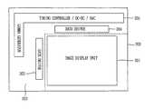
- FIG. 2is a plan view showing an array substrate according to the present invention.
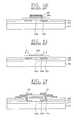
- FIGS. 3A to 3 Fshow procedures of fabricating a GOLDD type TFT, an LDD type TFT, and a PMOS according to the present invention.
- FIG. 4is a graph showing performance results illustrating variations of drain voltage and electric mobility of LDD type and GOLDD type TFTs according to the present invention.
- a liquid crystal display panelincludes an array substrate having unit pixels arranged therein as a matrix and a color filter substrate facing the array substrate. Liquid crystal is filled in the gap between the array substrate and the color filter substrate.
- the array substratemay be divided into an image display unit having unit pixels formed therein and a driving circuit unit for applying a driving signal to the image display unit.
- FIG. 2shows a structure of an array substrate of a liquid crystal display device according to the present invention.
- an image display unit 201is formed at a predetermined position on substrate 200
- driving circuit unit 202 equipped with various driving circuitsis positioned outside of the image display unit 201 .
- SOGSilicon on Glass
- a driving circuit unit driving a display region and a display region displaying the image on the same substratehas been developed with creation of a polycrystalline silicon TFT. Accordingly, processes for fabricating a liquid crystal display panel has been simplified making it possible to make compact liquid crystal panels using the SOG technique.
- One of the main factors for this processis the use of polysilicon as a channel of TFT. Polysilicon has superior electric conductivity relative to amorphous silicon. Therefore, a driving circuit unit and a switching device of an display region are formed using polysilicon TFT in which the polysilicon is adopted as a channel.
- a P-type TFT or an N-type TFTmay selectively be used as the switching device of the display region.
- a CMOSComplementary Metal Oxide Silicon
- NMOS and PMOS make a pairis used as a driving device of the driving circuit unit.
- the NMOSis an LDD type polysilicon TFT to control leakage current caused by carrier electrons.
- a driving circuit unitcan adopt the CMOS as a driving device.
- the CMOSmay be formed by using GOLDD type TFT instead of using LDD type NMOS. That is, the CMOS is configured in the driving circuit unit as a combination of LDD type TFT+PMOS and GOLDD type TFT+PMOS to prevent leakage current while optimizing a minimization of the driving circuit unit.
- the driving circuit unit 202 of the array substrate 200includes gate driver 203 for supplying gate signals to gate lines of the display region 201 and data driver 204 for applying data signals to data lines.
- the data linescross vertically to the gate lines, which are formed in the display region 201 .
- the two drivers 203 and 204are adjacent to the display region 201 .
- the driving circuit unit 202further includes a timing controller 205 for generating control signals to be supplied to the gate driver and the data driver by receiving signals inputted from the exterior.
- a DC-DC converterfor converting a DC voltage input from the exterior into a DC voltage required for driving the liquid crystal display panel
- a DA (Digital-to-Analog) converterfor converting a digital signal inputted from the exterior into an analog signal
- a gamma voltage generator and a common voltage (Vcom) driverfor adjusting a common voltage
- Various devices in the driving circuit unitare formed by CMOS.
- CMOScomplementary metal-oxide-semiconductor
- driving devices operating at a relatively high voltageare formed by CMOS using GOLDD type TFT to prevent leakage currents usually generated during operation at high voltages.
- Driving devices operating at a relatively low voltageare configured by CMOS using LDD type NMOS. As a result, driving stability and area reduction are achieved.
- an output buffer block within the gate driver, a level shifter in the driving circuit unit, a pixel switching TFT in the display region, and all other devices driven by high voltage more than 10Vare formed by CMOS adopting GOLDD type TFT.
- a timing controller, a shift resistor within the data driver, a DC-DC converter, a Vcom driver, and all other devices driven by a low voltage less than 10Vare formed by CMOS adopting LDD type TFT.
- the driving circuit unitmay be optimized for reliability and area reduction by utilizing both the LDD type TFT, which is capable of area reduction effect, and the GOLDD type TFT with superior reliability.
- the driving circuit unituses a CMOS having a pair of LDD type NMOS and PMOS and another CMOS having a pair of GOLDD type TFT and PMOS.
- CMOShaving a pair of LDD type NMOS and PMOS
- GOLDD type TFT and PMOSthe fabrication processes for LDD type NMOS, GOLDD type TFT and PMOS will be explained.
- active layers 302 a, 302 b, and 302 care formed respectively on predetermined regions (i.e., LDD type TFT region L, GOLDD type TFT region G, and PMOS region P) of a transparent substrate 301 .
- a process for forming the active layers 302 a, 302 b, and 302 cis achieved by forming an amorphous silicon layer on the substrate 301 using PECVD (Plasma Enhanced Chemical Vapor Deposition) method and patterning the amorphous silicon layer by a photomask process.
- the process for forming the active layers 302 a, 302 b, and 302 cincludes the steps of depositing the amorphous silicon layer on the substrate 301 by the PECVD method, coating a photoresist (not shown) on the amorphous silicon layer, exposing and developing the photoresist by applying a mask, and patterning the amorphous silicon by using the developed photoresist pattern.
- photoresist patterns 304are formed on the active layers 302 a, 302 b, and 302 c through a photomask process.
- the photoresist patterns 304define channel regions for the active layers 302 a and 302 b on the LDD type TFT region L and the GOLDD type TFT region G, and cover the entire active layer 302 c on the PMOS region.
- the photoresist patterns 304 on the active layers 302 a and 302 bcover each channel region 303 c of the active layers 302 a and 302 b and expose the residual regions.
- low concentration impurity ionis injected by using the photoresist pattern 304 as an impurity blocking mask.
- Group five elementsuch as phosphorous (P) may be used as the impurity ion injected.
- Pphosphorous
- low concentration impurity ionis injected into exposed parts of the active layers 302 a and 302 b on the LDD type TFT region L and the GOLDD type TFT region G, namely, regions which are not covered with the photoresist 304 . Accordingly, no impurity ion is injected into the active layer 302 c on the PMOS region P since it is covered with the photoresist pattern 304 .
- a gate insulating layer 305 made of a silicon oxide film (SiO2)is formed over the active layers 302 a, 302 b, and 302 c by the (PECVD) method.
- a metal layer, such as aluminum (Al) or the like,is formed on the gate insulating layer 305 .
- gate electrodes 306 , 307 , and 308are formed thereon.
- Gate electrode 307 formed on the GOLDD type TFT region Gis bigger than the gate electrode 306 formed on the LDD type TFT region L. This is to form low concentration impurity regions under the gate electrode 307 on the GOLDD type TFT region G.
- photoresist patterns 309 a and 309 bare formed on the gate electrodes 306 and 308 .
- the photoresist pattern 309 acovers the entire gate electrode 306 and a part of the low concentration impurity region 303 a and 303 b of the LDD type TFT region L.
- the photoresist pattern 309 bis formed on the PMOS region P to cover the entire PMOS region. No photoresist pattern is not formed on the GOLDD type TFT region G.
- high concentration impurity ionis injected into exposed low concentration impurity regions 303 a and 303 b of the LDD type TFT region L and the GOLDD type TFT region G.
- high concentration impurity regions 310 b and 310 c, the source and drain regions, respectivelyare formed in the LDD type TFT region L.
- LDD region 310 ais defined at adjacent regions of the channel.
- high concentration impurity regions 311 b and 311 c, the source and drain regions, respectivelyare formed in low concentration impurity regions 303 a and 303 b of the GOLDD type TFT region G.
- Low concentration impurity region 311 a under the gate electrode 307is defined as LDD region 311 a.
- the injected high concentration impurity ionmay be group five element such as phosphorous (P). While the source and drain regions of the LDD type TFT region L and the GOLDD type TFT region G are formed by injecting the high concentration impurity ion, the active layer on the PMOS region P is covered with the photoresist to prevent the impurity from getting injected thereinto.
- both the LDD type TFT region L and the GOLDD type TFT region Gare covered with photoresist pattern 312 .
- the PMOS region Pis not covered with the photoresist.
- a high concentration impurity ion of group three element such as boron (B)is injected into these regions using photoresist 312 as a blocking mask.
- the high concentration P type impurity ionis injected into source and drain regions 313 a and 313 b of the PMOS region P to thereby form a PMOS.
- LDD type NMOS, GOLDD type TFT, and PMOSare formed.
- the LDD type NMOSis formed at low voltage driving device regions using less than 10V
- the GOLDD type TFTis formed at relatively high voltage driving device regions using more than 10V.
- a CMOSis formed by making the LDD type NMOS and the PMOS a pair while simultaneously another CMOS is formed by making the GOLDD type TFT and the PMOS a pair.
- FIG. 3Fis an example of a configuration for the CMOS connecting the GOLDD type TFT and the PMOS.
- an insulating layer 314is formed over the entire substrate, and contact holes for exposing the source and drain regions of the TFT are formed on the insulating layer 314 .
- source electrode 320 and drain electrode 321 connected to the source and drain regions through the contact holesare formed.
- a common drain electrode 315is formed to connect the drain electrode 313 b on the PMOS and the drain electrode 311 c on the GOLDD type TFT.
- a passivation layer 317is formed on the source and drain electrodes, and a drain connection terminal 316 connected to the common drain electrode 315 is formed.
- the TFT as a switching device of the display regionmay be formed simultaneously with the above fabrication process for the CMOS in the driving circuit unit.
- the TFT in the display regionmay be formed by selecting either the PMOS or the NMOS.
- the GOLDD type TFT with superior reliabilitymay be used as the switching device.
- the driving circuit unit integrated liquid crystal panel including both the LDD type TFT and the GOLDD type TFTmay be achieved.
- the CMOS adopting the GOLDD type TFTis formed in devices driven by a relatively high driving voltage, while another CMOS adopting the LDD type TFT is formed in devices driven by a relatively low driving voltage.
- the driving circuit unit integrated liquid crystal panelwhich satisfy both an area reduction of the driving circuit unit and reliability thereof can be fabricated. Furthermore, since these processes are carried out without extraneous mask processes, efficiencies in fabrication of the liquid crystal panel is improved.
- FIG. 4is a graph showing an experimental result that illustrates variations of drain voltage and electric mobility of LDD type and GOLDD type TFTs for which width and length of a channel is 4 ⁇ m, respectively, and length of an LDD region is 1.5 ⁇ m.
- the graphillustrates the the variations of electric mobility of the LDD type TFT as compared to that of the GOLDD type TFT.
- the drain voltage at which the electric mobility becomes unstablevaries based on the dimensions of the TFT devices. Considering these characteristics of the variations of the drain voltage and the electric mobility, the LDD type TFT is used when the variation of the electric mobility of the polysilicon TFT is less than 7% while the GOLDD type TFT is used when the variation of the electric mobility is more than 7%. Thus, a driving circuit integrated liquid crystal display panel, which simultaneously satisfies reduction of dimension and increase in reliability of the driving circuit unit can be fabricated.
Landscapes
- Physics & Mathematics (AREA)
- Nonlinear Science (AREA)
- Mathematical Physics (AREA)
- Chemical & Material Sciences (AREA)
- Crystallography & Structural Chemistry (AREA)
- General Physics & Mathematics (AREA)
- Optics & Photonics (AREA)
- Liquid Crystal (AREA)
- Engineering & Computer Science (AREA)
- Microelectronics & Electronic Packaging (AREA)
- Thin Film Transistor (AREA)
- Liquid Crystal Display Device Control (AREA)
Abstract
Description
- This application claims the benefit of Korean Application No. 2004-39340 filed in Korea on May 31, 2004, which is hereby incorporated by reference in its entirety.
- 1. Field of the Invention
- The present invention relates to a liquid crystal display device and a fabrication method thereof, and particularly, to a liquid crystal display device having both GOLDD (Gate Overlapped Lightly Doped Drain) type and LDD (Lightly Doped Drain) type thin film transistors and a fabrication method thereof.
- 2. Description of the Related Art
- Recently, research for lighter, more compact flat panel display devices have resulted in liquid crystal display (LCD) devices being mass-produced and widely used. LCD devices usually use thin film transistors (TFT). TFTs in a LCD device are used as switching devices to individually drive each respective pixel. A TFT includes a semiconductor layer having a channel formed therein through which a current flows, a gate electrode for controlling the currently by applying a scanning signal to turn the current on and off a source electrode for inputting data signals, and a drain electrode for outputting data signals.
- The LCD includes a pixel region having a plurality of pixels therein for displaying real images, and a driving circuit unit for applying various signals to the pixel region. The TFT makes up all of the pixel region and the driving circuit unit. For Chip On Glass (COG) type LCD, which has the driving circuit unit and pixel region on the same substrate, research to form a compact LCD has been mainly achieved by providing the driving circuit unit with a polycrystalline TFT.
- The TFT formed in the driving circuit unit has to have higher electric mobility as compared with the TFT formed in the pixel region. Accordingly, the polycrystalline TFT having high electric mobility is usually applied in the driving circuit unit.
- Recently, attempts have been made to further minimize the LCD to form a lighter and more compact display apparatus. However, since the pixel region in which images are displayed cannot be further reduced, (the size of this pixel region has already been established), the size reduction of the LCD is substantially achieved by reducing the area of the driving circuit unit. Thus, when the area of the driving circuit unit is reduced, the size of the TFT arranged in the driving circuit unit is inevitably reduced as well. The reduction of the TFT is achieved by reducing the length of the channel. Reducing the length of the channel, however, make the channel layer prone to damage by generating hot carriers on the channel. The hot carriers trapped within the channel change the threshold voltage of a device creating a defect.
- To solve this problem, a LDD (Lightly Doped drain) type TFT has been introduced. The LDD type TFT has a low concentration impurity region. The LDD region is formed adjacent to the channel layer and a high concentration impurity region is formed outside of the LDD region. Furthermore, since LDD type TFT hardly generates any off current, it may prevent leakage currents that cause degradation of image quality.
- However, in the LDD type TFT, there is a limit on how much the channel length can be reduced. Reliability of the TFT declines as the channel length gets shorter. Therefore, when the TFT having short channel length is applied to display apparatuses of high image qualities such as HDTV, the channel may be damaged due to hot carrier effects.
- A TFT having a GOLDD (Gate Overlapped LDD) type is proposed to solve those problems. In the GOLDD type TFT, since a gate electrode is overlapped with an LDD region, it is possible to form a short channel. As a result, a small-sized TFT with reliability can be fabricated.
- Hereinafter, a fabrication process for the GOLDD type TFT according to the related art is discussed with reference to
FIGS. 1A through 1F . - First, as shown in
FIG. 1A , abuffer layer 102 is formed on asubstrate 101, which is made of a transparent material like glass. Next, asemiconductor layer 103 is formed on thebuffer layer 102 by depositing an amorphous semiconductor such as a silicon and patterning it. Thereafter, aphotoresist pattern 104 is formed on thesemiconductor layer 103 and then low concentration impurity ion (i.e., n− ion) is injected into the exposed region of thesemiconductor layer 103 not blocked by the photoresist pattern. The result is the formation of achannel layer 103aand lowconcentration impurity region 103b,the n− region. - Next, as shown in
FIG. 1B , after removing thephotoresist pattern 104 on thechannel layer 103a,a laser beam is irradiated on thesemiconductor layer 103 to crystallize the amorphous semiconductor layer. When the laser beam is irradiated on thesemiconductor layer 103, the impurity ion injected in the n−region 103bis activated. - Next, as shown in
FIG. 1C , agate insulating layer 105 is formed on thesemiconductor layer 103. Thereafter, ametal layer 106 is formed on thegate insulating layer 105. - Referring to
FIG. 1D , aphotoresist pattern 107 is formed on themetal layer 106 and photolithography process is performed to creategate electrode 106a.The size of thegate electrode 106ais greater than thechannel layer 103a. - Next, referring to
FIG. 1E , high concentration impurity ion (n+ ion) is injected into the n−region 103bby using thegate electrode 106aas a mask. A part of each n−layer 103b(i.e., regions where are not blocked by thegate electrode 106a) becomes highconcentration impurity region 103c(n+ region). As a result, thegate electrode 106ais overlapped with lowconcentration impurity regions 103b′. - After forming the high
concentration impurity layer 103c,as shown inFIG. 1F , apassivation layer 108 is formed on thegate electrode 106a.A conductive layer is deposited on thepassivation layer 108 and is etched to form asource electrode 109 and adrain electrode 110. - The
source electrode 109 and thedrain electrode 110 are connected to the n+region 103crespectively through contact holes exposing then+ region 103c. - Accordingly, the GOLDD type TFT has low concentration impurity ion region and high concentration impurity ion region similar to that of LDD type TFT. The GOLDD type TFT has superior reliability but cannot readily be reduced in size. On the other hand, the LDD type TFT is advantageous for its small-size but its reliability is degraded due to minimization.
- Accordingly, the present invention is directed to a liquid crystal display device that substantially obviates one or more of the problems due to limitations and disadvantages of the related art.
- Therefore, an object of the present invention is to form a more compact liquid crystal display device by decreasing the area of a driving circuit unit in a substrate. More particularly, an object of the present invention is to form an optimal driving circuit unit and a more compact liquid crystal display device by selectively applying LDD type TFT and GOLDD type TFT to various driving devices formed in the driving circuit unit according to driving voltages thereof.
- Additional features and advantages of the invention will be set forth in the description which follows, and in part will be apparent from the description, or may be learned by practice of the invention. The objectives and other advantages of the invention will be realized and attained by the structure particularly pointed out in the written description and claims hereof as well as the appended drawings.
- To achieve these and other advantages in accordance with the purpose of the present invention as embodied and broadly described herein, a liquid crystal display device includes a display region having unit pixels arranged thereon in a matrix, and a driving circuit unit having at least a LDD (Lightly Doped Drain) type TFT and a GOLDD (Gate overlapped Lightly Doped Drain) type TFT.
- In another aspect, a liquid crystal display device includes an image display unit having unit pixels arranged thereon in a matrix, and a driving circuit unit formed by a first CMOS including LDD type TFT and a second CMOS including GOLDD type TFT according to a driving voltage.
- In yet another aspect, a method for fabricating a driving circuit unit integrated liquid crystal display device includes the steps of designating a display region and a driving circuit region on a substrate, forming unit pixels in the display region in a matrix, forming at least one driving unit in the driving circuit region, the driving unit including a first driving section, a second driving section, and a third driving section, forming a LDD type NMOS in the first driving section, a GOLDD type TFT in the second driving section, and a PMOS in the third driving section, and simultaneously forming a first CMOS by paring the LDD type NMOS with the PMOS and a second CMOS by pairing the GOLDD type TFT with the PMOS.
- It is to be understood that both the foregoing general description and the following detailed description are exemplary and explanatory and are intended to provide further explanation of the invention as claimed.
- The accompanying drawings, which are included to provide a further understanding of the invention and are incorporated in and constitute a part of this specification, illustrate embodiments of the invention and together with the description serve to explain the principles of the invention. In the drawings:
FIGS. 1A to1F show procedures of fabricating a GOLDD type TFT according to the related art;FIG. 2 is a plan view showing an array substrate according to the present invention;FIGS. 3A to3F show procedures of fabricating a GOLDD type TFT, an LDD type TFT, and a PMOS according to the present invention; andFIG. 4 is a graph showing performance results illustrating variations of drain voltage and electric mobility of LDD type and GOLDD type TFTs according to the present invention.- Reference will now be made in detail to the preferred embodiments of the present invention, examples of which are illustrated in the accompanying drawings.
- In general, a liquid crystal display panel includes an array substrate having unit pixels arranged therein as a matrix and a color filter substrate facing the array substrate. Liquid crystal is filled in the gap between the array substrate and the color filter substrate. The array substrate may be divided into an image display unit having unit pixels formed therein and a driving circuit unit for applying a driving signal to the image display unit.
FIG. 2 shows a structure of an array substrate of a liquid crystal display device according to the present invention. As shown inFIG. 2 , animage display unit 201 is formed at a predetermined position onsubstrate 200, and drivingcircuit unit 202 equipped with various driving circuits is positioned outside of theimage display unit 201.- Particularly, SOG (Silicon on Glass) technique to form a driving circuit unit driving a display region and a display region displaying the image on the same substrate has been developed with creation of a polycrystalline silicon TFT. Accordingly, processes for fabricating a liquid crystal display panel has been simplified making it possible to make compact liquid crystal panels using the SOG technique. One of the main factors for this process is the use of polysilicon as a channel of TFT. Polysilicon has superior electric conductivity relative to amorphous silicon. Therefore, a driving circuit unit and a switching device of an display region are formed using polysilicon TFT in which the polysilicon is adopted as a channel.
- A P-type TFT or an N-type TFT may selectively be used as the switching device of the display region. A CMOS (Complementary Metal Oxide Silicon) in which NMOS and PMOS make a pair is used as a driving device of the driving circuit unit. Specifically, the NMOS is an LDD type polysilicon TFT to control leakage current caused by carrier electrons.
- A driving circuit unit can adopt the CMOS as a driving device. Here, the CMOS may be formed by using GOLDD type TFT instead of using LDD type NMOS. That is, the CMOS is configured in the driving circuit unit as a combination of LDD type TFT+PMOS and GOLDD type TFT+PMOS to prevent leakage current while optimizing a minimization of the driving circuit unit.
- As shown in
FIG. 2 , the drivingcircuit unit 202 of thearray substrate 200 includesgate driver 203 for supplying gate signals to gate lines of thedisplay region 201 anddata driver 204 for applying data signals to data lines. The data lines cross vertically to the gate lines, which are formed in thedisplay region 201. The twodrivers display region 201. - The driving
circuit unit 202 further includes atiming controller 205 for generating control signals to be supplied to the gate driver and the data driver by receiving signals inputted from the exterior. To supply the generated control signals to the gate and data drivers, a DC-DC converter for converting a DC voltage input from the exterior into a DC voltage required for driving the liquid crystal display panel, a DA (Digital-to-Analog) converter for converting a digital signal inputted from the exterior into an analog signal, a gamma voltage generator and a common voltage (Vcom) driver for adjusting a common voltage are also included. Various devices in the driving circuit unit are formed by CMOS. - In forming the CMOS, driving devices operating at a relatively high voltage are formed by CMOS using GOLDD type TFT to prevent leakage currents usually generated during operation at high voltages. Driving devices operating at a relatively low voltage are configured by CMOS using LDD type NMOS. As a result, driving stability and area reduction are achieved.
- For instance, an output buffer block within the gate driver, a level shifter in the driving circuit unit, a pixel switching TFT in the display region, and all other devices driven by high voltage more than 10V are formed by CMOS adopting GOLDD type TFT. On the other hand, a timing controller, a shift resistor within the data driver, a DC-DC converter, a Vcom driver, and all other devices driven by a low voltage less than 10V are formed by CMOS adopting LDD type TFT. Using these configurations, the driving circuit unit may be optimized for reliability and area reduction by utilizing both the LDD type TFT, which is capable of area reduction effect, and the GOLDD type TFT with superior reliability.
- Hereinafter, the CMOS fabrication process for the driving circuit unit will be explained with reference to
FIGS. 3A to3F. - The driving circuit unit according to the present invention uses a CMOS having a pair of LDD type NMOS and PMOS and another CMOS having a pair of GOLDD type TFT and PMOS. For reference, the fabrication processes for LDD type NMOS, GOLDD type TFT and PMOS will be explained.
- First, referring to
FIG. 3A ,active layers transparent substrate 301. - A process for forming the
active layers substrate 301 using PECVD (Plasma Enhanced Chemical Vapor Deposition) method and patterning the amorphous silicon layer by a photomask process. In other words, the process for forming theactive layers substrate 301 by the PECVD method, coating a photoresist (not shown) on the amorphous silicon layer, exposing and developing the photoresist by applying a mask, and patterning the amorphous silicon by using the developed photoresist pattern. - As shown in
FIG. 3B , after forming theactive layers photoresist patterns 304 are formed on theactive layers photoresist patterns 304 define channel regions for theactive layers active layer 302con the PMOS region. Thephotoresist patterns 304 on theactive layers channel region 303cof theactive layers - Afterwards, low concentration impurity ion is injected by using the
photoresist pattern 304 as an impurity blocking mask. Group five element such as phosphorous (P) may be used as the impurity ion injected. According to the ion injection, low concentration impurity ion is injected into exposed parts of theactive layers photoresist 304. Accordingly, no impurity ion is injected into theactive layer 302con the PMOS region P since it is covered with thephotoresist pattern 304. - Thereafter, as shown in
FIG. 3C , agate insulating layer 305 made of a silicon oxide film (SiO2) is formed over theactive layers gate insulating layer 305. Through the photolithography process,gate electrodes Gate electrode 307 formed on the GOLDD type TFT region G is bigger than thegate electrode 306 formed on the LDD type TFT region L. This is to form low concentration impurity regions under thegate electrode 307 on the GOLDD type TFT region G. - Next, as shown in to
FIG. 3D ,photoresist patterns gate electrodes photoresist pattern 309acovers theentire gate electrode 306 and a part of the lowconcentration impurity region photoresist pattern 309bis formed on the PMOS region P to cover the entire PMOS region. No photoresist pattern is not formed on the GOLDD type TFT region G. - Next, high concentration impurity ion is injected into exposed low
concentration impurity regions concentration impurity regions L. LDD region 310ais defined at adjacent regions of the channel. Moreover, highconcentration impurity regions concentration impurity regions concentration impurity region 311aunder thegate electrode 307 is defined asLDD region 311a.The injected high concentration impurity ion may be group five element such as phosphorous (P). While the source and drain regions of the LDD type TFT region L and the GOLDD type TFT region G are formed by injecting the high concentration impurity ion, the active layer on the PMOS region P is covered with the photoresist to prevent the impurity from getting injected thereinto. - Next, as shown in
FIG. 3E , both the LDD type TFT region L and the GOLDD type TFT region G are covered withphotoresist pattern 312. Here, the PMOS region P is not covered with the photoresist. - Next, a high concentration impurity ion of group three element such as boron (B) is injected into these
regions using photoresist 312 as a blocking mask. At this time, the high concentration P type impurity ion is injected into source and drainregions - Next, as shown in
FIG. 3F , a CMOS is formed by making the LDD type NMOS and the PMOS a pair while simultaneously another CMOS is formed by making the GOLDD type TFT and the PMOS a pair.FIG. 3F is an example of a configuration for the CMOS connecting the GOLDD type TFT and the PMOS. - After completing the TFT, an insulating
layer 314 is formed over the entire substrate, and contact holes for exposing the source and drain regions of the TFT are formed on the insulatinglayer 314. - Next,
source electrode 320 anddrain electrode 321 connected to the source and drain regions through the contact holes are formed. In this step of forming thesource electrode 320 and thedrain electrode 321, acommon drain electrode 315 is formed to connect thedrain electrode 313bon the PMOS and thedrain electrode 311con the GOLDD type TFT. - Next, a
passivation layer 317 is formed on the source and drain electrodes, and adrain connection terminal 316 connected to thecommon drain electrode 315 is formed. Meanwhile, the TFT as a switching device of the display region may be formed simultaneously with the above fabrication process for the CMOS in the driving circuit unit. The TFT in the display region may be formed by selecting either the PMOS or the NMOS. Furthermore, when the switching device of the image display unit is driven at a high voltage, the GOLDD type TFT with superior reliability may be used as the switching device. As a result, the driving circuit unit integrated liquid crystal panel including both the LDD type TFT and the GOLDD type TFT may be achieved. - In fabricating the driving circuit unit integrated liquid crystal panel according to the present invention, the CMOS adopting the GOLDD type TFT is formed in devices driven by a relatively high driving voltage, while another CMOS adopting the LDD type TFT is formed in devices driven by a relatively low driving voltage. As a result, the driving circuit unit integrated liquid crystal panel which satisfy both an area reduction of the driving circuit unit and reliability thereof can be fabricated. Furthermore, since these processes are carried out without extraneous mask processes, efficiencies in fabrication of the liquid crystal panel is improved.
- In accordance with an exemplary embodiment of the present invention, among TFTs positioned in the driving circuit unit, a GOLDD type TFT is driven by a high voltage more than 10V and an LDD type TFT is driven by a low voltage less than 10V.
FIG. 4 is a graph showing an experimental result that illustrates variations of drain voltage and electric mobility of LDD type and GOLDD type TFTs for which width and length of a channel is 4 μm, respectively, and length of an LDD region is 1.5 μm. The graph illustrates the the variations of electric mobility of the LDD type TFT as compared to that of the GOLDD type TFT. - As shown in
FIG. 4 , when the drain voltage Vd becomes greater than 10V, the electric mobility of the LDD type TFT having the above-described dimensions varies drastically while that of the GOLDD type TFT having the above-described dimensions remains relatively stable. This experimental result demonstrates that application of CMOS composed of the GOLDD type device is preferred for circuits requiring a high driving voltage to increase reliability. For circuits requiring a low driving voltage, application of CMOS composed of the LDD type device is preferred since LDD type devices are relatively smaller in size than the GOLDD type device while reliability is not affected. - The drain voltage at which the electric mobility becomes unstable varies based on the dimensions of the TFT devices. Considering these characteristics of the variations of the drain voltage and the electric mobility, the LDD type TFT is used when the variation of the electric mobility of the polysilicon TFT is less than 7% while the GOLDD type TFT is used when the variation of the electric mobility is more than 7%. Thus, a driving circuit integrated liquid crystal display panel, which simultaneously satisfies reduction of dimension and increase in reliability of the driving circuit unit can be fabricated.
- It will be apparent to those skilled in the art that various modifications and variations can be made in the liquid crystal display device of the present invention and the method of fabricating the same without departing from the spirit or scope of the invention. Thus, it is intended that the present invention cover the modifications and variations of this invention provided they come within the scope of the appended claims and their equivalents.
Claims (15)
Applications Claiming Priority (3)
| Application Number | Priority Date | Filing Date | Title |
|---|---|---|---|
| KR10-2004-0039340 | 2004-05-31 | ||
| KR1020040039340AKR100675636B1 (en) | 2004-05-31 | 2004-05-31 | A liquid crystal display with integrated driving circuit unit including a TFT structure and a TFT structure simultaneously. |
| KR39340/2004 | 2004-05-31 |
Publications (2)
| Publication Number | Publication Date |
|---|---|
| US20050266595A1true US20050266595A1 (en) | 2005-12-01 |
| US8692750B2 US8692750B2 (en) | 2014-04-08 |
Family
ID=35425870
Family Applications (1)
| Application Number | Title | Priority Date | Filing Date |
|---|---|---|---|
| US11/139,980Expired - Fee RelatedUS8692750B2 (en) | 2004-05-31 | 2005-05-31 | Liquid crystal display device having GOLDD type TFT and LDD type TFT and method of making same |
Country Status (4)
| Country | Link |
|---|---|
| US (1) | US8692750B2 (en) |
| JP (1) | JP5016789B2 (en) |
| KR (1) | KR100675636B1 (en) |
| CN (1) | CN100381926C (en) |
Cited By (7)
| Publication number | Priority date | Publication date | Assignee | Title |
|---|---|---|---|---|
| US20090002312A1 (en)* | 2007-06-28 | 2009-01-01 | Samsung Electronics Co., Ltd | Display apparatus, method of driving the same, and sensing driver of display apparatus |
| US20110122052A1 (en)* | 2009-11-23 | 2011-05-26 | Yu-Cheng Chen | Display device |
| US20110193168A1 (en)* | 2008-10-27 | 2011-08-11 | Sharp Kabushiki Kaisha | Semiconductor device and method for manufacturing same |
| US20110292003A1 (en)* | 2010-05-27 | 2011-12-01 | Fih (Hong Kong) Limited | Stylus |
| CN103441128A (en)* | 2013-05-27 | 2013-12-11 | 南京中电熊猫液晶显示科技有限公司 | TFT array substrate and manufacturing method thereof |
| US8658460B2 (en) | 2011-06-21 | 2014-02-25 | Samsung Display Co., Ltd. | Organic light-emitting display device and method of manufacturing the same |
| US9419029B1 (en)* | 2014-05-06 | 2016-08-16 | Shenzhen China Star Optoelectronics Technology Co., Ltd. | Method for manufacturing thin film transistor array substrate and thin film transistor array substrate for the same |
Families Citing this family (3)
| Publication number | Priority date | Publication date | Assignee | Title |
|---|---|---|---|---|
| KR102235421B1 (en)* | 2013-12-06 | 2021-04-01 | 엘지디스플레이 주식회사 | Array substrate and method of fabricating the same |
| KR102060377B1 (en)* | 2014-01-27 | 2020-02-11 | 한국전자통신연구원 | A Display device, method of fabricating the same, and method of fabricating an image sensor device |
| CN112635571B (en)* | 2019-09-24 | 2024-08-02 | 乐金显示有限公司 | Thin film transistor, method for manufacturing the same, and display device including the same |
Citations (23)
| Publication number | Priority date | Publication date | Assignee | Title |
|---|---|---|---|---|
| US5198379A (en)* | 1990-04-27 | 1993-03-30 | Sharp Kabushiki Kaisha | Method of making a MOS thin film transistor with self-aligned asymmetrical structure |
| US5485019A (en)* | 1992-02-05 | 1996-01-16 | Semiconductor Energy Laboratory Co., Ltd. | Semiconductor device and method for forming the same |
| US5521107A (en)* | 1991-02-16 | 1996-05-28 | Semiconductor Energy Laboratory Co., Ltd. | Method for forming a field-effect transistor including anodic oxidation of the gate |
| US5821559A (en)* | 1991-02-16 | 1998-10-13 | Semiconductor Energy Laboratory Co., Ltd. | Electric device, matrix device, electro-optical display device, and semiconductor memory having thin-film transistors |
| US5949107A (en)* | 1995-11-07 | 1999-09-07 | Semiconductor Energy Laboratory Co., Ltd. | Semiconductor device and method of fabricating same |
| US6180957B1 (en)* | 1993-07-26 | 2001-01-30 | Seiko Epson Corporation | Thin-film semiconductor device, and display system using the same |
| US6252248B1 (en)* | 1998-06-08 | 2001-06-26 | Sanyo Electric Co., Ltd. | Thin film transistor and display |
| US20010030722A1 (en)* | 1997-02-27 | 2001-10-18 | Seiko Epson Corporation | Apparatus for providing light shielding in a liquid crystal display |
| US20020014624A1 (en)* | 1998-12-28 | 2002-02-07 | Shunpei Yamazaki | Semiconductor device |
| US6362507B1 (en)* | 1999-04-20 | 2002-03-26 | Semiconductor Energy Laboratory Co., Ltd. | Electro-optical devices in which pixel section and the driver circuit are disposed over the same substrate |
| US20020070382A1 (en)* | 2000-12-11 | 2002-06-13 | Shunpei Yamazaki | Semiconductor device, and manufacturing method thereof |
| US6424012B1 (en)* | 1999-04-20 | 2002-07-23 | Semiconductor Energy Laboratory Co., Ltd. | Semiconductor device having a tantalum oxide blocking film |
| US6479333B1 (en)* | 1997-03-03 | 2002-11-12 | Semiconductor Energy Laboratory Co., Ltd. | Method of manufacturing a semiconductor device |
| US6512504B1 (en)* | 1999-04-27 | 2003-01-28 | Semiconductor Energy Laborayory Co., Ltd. | Electronic device and electronic apparatus |
| US20030057853A1 (en)* | 2000-08-24 | 2003-03-27 | Masumitsu Ino | Liquid crystal display device and electronic apparatus comprising it |
| US6603453B2 (en)* | 1998-06-12 | 2003-08-05 | Semiconductor Energy Laboratory Co., Ltd. | Semiconductor device and method for manufacturing the same |
| US6603455B1 (en)* | 1997-10-28 | 2003-08-05 | Semiconductor Energy Laboratory Co., Ltd. | Display panel drive circuit and display panel |
| US6740938B2 (en)* | 2001-04-16 | 2004-05-25 | Semiconductor Energy Laboratory Co., Ltd. | Transistor provided with first and second gate electrodes with channel region therebetween |
| US20040217354A1 (en)* | 2003-02-19 | 2004-11-04 | Takahiro Kamo | Display device and manufacturing method thereof |
| US6893503B1 (en)* | 1997-03-27 | 2005-05-17 | Semiconductor Energy Laboratory Co., Ltd. | Method of manufacturing a semiconductor device |
| US7038283B2 (en)* | 2001-08-02 | 2006-05-02 | Fujitsu Display Technologies Corporation | Thin film transistor device, method of manufacturing the same and liquid crystal panel |
| US7189997B2 (en)* | 2001-03-27 | 2007-03-13 | Semiconductor Energy Laboratory Co., Ltd. | Semiconductor device and method for manufacturing the same |
| US7233342B1 (en)* | 1999-02-24 | 2007-06-19 | Semiconductor Energy Laboratory Co., Ltd. | Time and voltage gradation driven display device |
Family Cites Families (9)
| Publication number | Priority date | Publication date | Assignee | Title |
|---|---|---|---|---|
| JPH08220505A (en)* | 1995-02-20 | 1996-08-30 | Sanyo Electric Co Ltd | Liquid crystal display |
| JPH10268254A (en)* | 1997-03-26 | 1998-10-09 | Seiko Epson Corp | Liquid crystal display |
| US6576926B1 (en)* | 1999-02-23 | 2003-06-10 | Semiconductor Energy Laboratory Co., Ltd. | Semiconductor device and fabrication method thereof |
| JP3983460B2 (en)* | 1999-07-06 | 2007-09-26 | 株式会社半導体エネルギー研究所 | Method for manufacturing semiconductor device |
| JP4666723B2 (en)* | 1999-07-06 | 2011-04-06 | 株式会社半導体エネルギー研究所 | Method for manufacturing semiconductor device |
| JP4801241B2 (en)* | 1999-07-22 | 2011-10-26 | 株式会社半導体エネルギー研究所 | Semiconductor device and manufacturing method thereof |
| JP3688548B2 (en)* | 2000-03-14 | 2005-08-31 | シャープ株式会社 | Image display device |
| JP4712155B2 (en)* | 2000-05-02 | 2011-06-29 | 株式会社半導体エネルギー研究所 | Method for manufacturing semiconductor device |
| KR100491141B1 (en)* | 2001-03-02 | 2005-05-24 | 삼성에스디아이 주식회사 | TFT and Method for Fabricating the Same and Active Matrix display device and Method for fabricating the Same using the TFT |
- 2004
- 2004-05-31KRKR1020040039340Apatent/KR100675636B1/ennot_activeExpired - Fee Related
- 2005
- 2005-05-20JPJP2005148581Apatent/JP5016789B2/ennot_activeExpired - Fee Related
- 2005-05-31USUS11/139,980patent/US8692750B2/ennot_activeExpired - Fee Related
- 2005-05-31CNCNB2005100723942Apatent/CN100381926C/ennot_activeExpired - Fee Related
Patent Citations (26)
| Publication number | Priority date | Publication date | Assignee | Title |
|---|---|---|---|---|
| US5198379A (en)* | 1990-04-27 | 1993-03-30 | Sharp Kabushiki Kaisha | Method of making a MOS thin film transistor with self-aligned asymmetrical structure |
| US5521107A (en)* | 1991-02-16 | 1996-05-28 | Semiconductor Energy Laboratory Co., Ltd. | Method for forming a field-effect transistor including anodic oxidation of the gate |
| US5821559A (en)* | 1991-02-16 | 1998-10-13 | Semiconductor Energy Laboratory Co., Ltd. | Electric device, matrix device, electro-optical display device, and semiconductor memory having thin-film transistors |
| US5485019A (en)* | 1992-02-05 | 1996-01-16 | Semiconductor Energy Laboratory Co., Ltd. | Semiconductor device and method for forming the same |
| US6180957B1 (en)* | 1993-07-26 | 2001-01-30 | Seiko Epson Corporation | Thin-film semiconductor device, and display system using the same |
| US5949107A (en)* | 1995-11-07 | 1999-09-07 | Semiconductor Energy Laboratory Co., Ltd. | Semiconductor device and method of fabricating same |
| US20010030722A1 (en)* | 1997-02-27 | 2001-10-18 | Seiko Epson Corporation | Apparatus for providing light shielding in a liquid crystal display |
| US6330044B1 (en)* | 1997-02-27 | 2001-12-11 | Seiko Epson Corporation | Apparatus for providing light shielding in a liquid crystal display |
| US6479333B1 (en)* | 1997-03-03 | 2002-11-12 | Semiconductor Energy Laboratory Co., Ltd. | Method of manufacturing a semiconductor device |
| US6893503B1 (en)* | 1997-03-27 | 2005-05-17 | Semiconductor Energy Laboratory Co., Ltd. | Method of manufacturing a semiconductor device |
| US6603455B1 (en)* | 1997-10-28 | 2003-08-05 | Semiconductor Energy Laboratory Co., Ltd. | Display panel drive circuit and display panel |
| US6252248B1 (en)* | 1998-06-08 | 2001-06-26 | Sanyo Electric Co., Ltd. | Thin film transistor and display |
| US6603453B2 (en)* | 1998-06-12 | 2003-08-05 | Semiconductor Energy Laboratory Co., Ltd. | Semiconductor device and method for manufacturing the same |
| US20020014624A1 (en)* | 1998-12-28 | 2002-02-07 | Shunpei Yamazaki | Semiconductor device |
| US7276730B2 (en)* | 1998-12-28 | 2007-10-02 | Semiconductor Energy Laboratory Co., Ltd. | Semiconductor device having a pixel matrix circuit that includes a pixel TFT and a storage capacitor |
| US7233342B1 (en)* | 1999-02-24 | 2007-06-19 | Semiconductor Energy Laboratory Co., Ltd. | Time and voltage gradation driven display device |
| US6424012B1 (en)* | 1999-04-20 | 2002-07-23 | Semiconductor Energy Laboratory Co., Ltd. | Semiconductor device having a tantalum oxide blocking film |
| US6362507B1 (en)* | 1999-04-20 | 2002-03-26 | Semiconductor Energy Laboratory Co., Ltd. | Electro-optical devices in which pixel section and the driver circuit are disposed over the same substrate |
| US6512504B1 (en)* | 1999-04-27 | 2003-01-28 | Semiconductor Energy Laborayory Co., Ltd. | Electronic device and electronic apparatus |
| US20030057853A1 (en)* | 2000-08-24 | 2003-03-27 | Masumitsu Ino | Liquid crystal display device and electronic apparatus comprising it |
| US6953951B2 (en)* | 2000-12-11 | 2005-10-11 | Semiconductor Energy Laboratory Co., Ltd. | Semiconductor device, and manufacturing method thereof |
| US20020070382A1 (en)* | 2000-12-11 | 2002-06-13 | Shunpei Yamazaki | Semiconductor device, and manufacturing method thereof |
| US7189997B2 (en)* | 2001-03-27 | 2007-03-13 | Semiconductor Energy Laboratory Co., Ltd. | Semiconductor device and method for manufacturing the same |
| US6740938B2 (en)* | 2001-04-16 | 2004-05-25 | Semiconductor Energy Laboratory Co., Ltd. | Transistor provided with first and second gate electrodes with channel region therebetween |
| US7038283B2 (en)* | 2001-08-02 | 2006-05-02 | Fujitsu Display Technologies Corporation | Thin film transistor device, method of manufacturing the same and liquid crystal panel |
| US20040217354A1 (en)* | 2003-02-19 | 2004-11-04 | Takahiro Kamo | Display device and manufacturing method thereof |
Cited By (11)
| Publication number | Priority date | Publication date | Assignee | Title |
|---|---|---|---|---|
| US20090002312A1 (en)* | 2007-06-28 | 2009-01-01 | Samsung Electronics Co., Ltd | Display apparatus, method of driving the same, and sensing driver of display apparatus |
| US8253699B2 (en) | 2007-06-28 | 2012-08-28 | Samsung Electronics Co., Ltd. | Display apparatus, method of driving the same, and sensing driver of display apparatus |
| US20110193168A1 (en)* | 2008-10-27 | 2011-08-11 | Sharp Kabushiki Kaisha | Semiconductor device and method for manufacturing same |
| US8357977B2 (en) | 2008-10-27 | 2013-01-22 | Sharp Kabushiki Kaisha | Semiconductor device and method for manufacturing same |
| US20110122052A1 (en)* | 2009-11-23 | 2011-05-26 | Yu-Cheng Chen | Display device |
| US9070334B2 (en)* | 2009-11-23 | 2015-06-30 | Au Optronics Corp. | Display device |
| US20110292003A1 (en)* | 2010-05-27 | 2011-12-01 | Fih (Hong Kong) Limited | Stylus |
| US8593437B2 (en)* | 2010-05-27 | 2013-11-26 | Shenzhen Futaihong Precision Industry Co., Ltd. | Stylus having retracted and extended positions |
| US8658460B2 (en) | 2011-06-21 | 2014-02-25 | Samsung Display Co., Ltd. | Organic light-emitting display device and method of manufacturing the same |
| CN103441128A (en)* | 2013-05-27 | 2013-12-11 | 南京中电熊猫液晶显示科技有限公司 | TFT array substrate and manufacturing method thereof |
| US9419029B1 (en)* | 2014-05-06 | 2016-08-16 | Shenzhen China Star Optoelectronics Technology Co., Ltd. | Method for manufacturing thin film transistor array substrate and thin film transistor array substrate for the same |
Also Published As
| Publication number | Publication date |
|---|---|
| KR100675636B1 (en) | 2007-02-02 |
| US8692750B2 (en) | 2014-04-08 |
| JP2005346053A (en) | 2005-12-15 |
| CN100381926C (en) | 2008-04-16 |
| KR20050114126A (en) | 2005-12-05 |
| JP5016789B2 (en) | 2012-09-05 |
| CN1704827A (en) | 2005-12-07 |
Similar Documents
| Publication | Publication Date | Title |
|---|---|---|
| KR100550693B1 (en) | Electro optical substrate device and manufacturing method for same, electro optical apparatus, electronic apparatus and manufacturing method for a substrate device | |
| CN100440569C (en) | Current-driven light-emitting display device and manufacturing method thereof | |
| US6633359B1 (en) | Liquid crystal display having signal lines on substrate intermittently extending and its manufacture | |
| US5940151A (en) | Liquid crystal display and method for fabricating the same | |
| US8035596B2 (en) | Liquid crystal display device | |
| US20070045627A1 (en) | Thin film transistor substrate and method of manufacturing the same | |
| JP4211644B2 (en) | Manufacturing method of electro-optical device | |
| WO1999035678A1 (en) | Semiconductor device, substrate for electro-optical device, electro-optical device, electronic device, and projection display | |
| JP2009289928A (en) | Drive circuit, active matrix substrate, and liquid crystal display device | |
| KR100626134B1 (en) | Thin Film Transistors, Active Matrix Substrates, Display Devices, and Electronic Devices | |
| US8692750B2 (en) | Liquid crystal display device having GOLDD type TFT and LDD type TFT and method of making same | |
| JP2010039229A (en) | Display device | |
| JPH0982969A (en) | Thin film transistor and liquid crystal display | |
| EP1074047A4 (en) | METHOD FOR MANUFACTURING A SILICON LIGHT MODULATOR ON ELECTRICALLY ADDRESSABLE SAPPHIRE | |
| US8269905B2 (en) | Electronic device, manufacturing method of the same and electronic apparatus | |
| US20110186848A1 (en) | Semiconductor device and display device | |
| JP4641741B2 (en) | Semiconductor device | |
| JPH10111520A (en) | Liquid crystal display panel and electronic device using the same | |
| WO2010050160A1 (en) | Semiconductor device and method for manufacturing same | |
| JP5337414B2 (en) | Display device and manufacturing method thereof | |
| US8168981B2 (en) | Display substrate having stepped data line and a liquid crystal display device having the same | |
| JP2010010161A (en) | Display device, and method of manufacturing the same | |
| JP3777873B2 (en) | Thin film transistor, active matrix substrate, electro-optical device, and electronic apparatus | |
| JPH10111521A (en) | Manufacturing method of liquid crystal display panel, liquid crystal display panel, and electronic equipment using the same | |
| JP2006253173A (en) | Electrooptical device and manufacturing method thereof, and electronic equipment |
Legal Events
| Date | Code | Title | Description |
|---|---|---|---|
| AS | Assignment | Owner name:LG.PHILIPS LCD CO., LTD., KOREA, REPUBLIC OF Free format text:ASSIGNMENT OF ASSIGNORS INTEREST;ASSIGNOR:LEE, SEOK-WOO;REEL/FRAME:016860/0741 Effective date:20050707 | |
| AS | Assignment | Owner name:LG DISPLAY CO., LTD., KOREA, REPUBLIC OF Free format text:CHANGE OF NAME;ASSIGNOR:LG.PHILIPS LCD CO., LTD.;REEL/FRAME:021147/0009 Effective date:20080319 Owner name:LG DISPLAY CO., LTD.,KOREA, REPUBLIC OF Free format text:CHANGE OF NAME;ASSIGNOR:LG.PHILIPS LCD CO., LTD.;REEL/FRAME:021147/0009 Effective date:20080319 | |
| FEPP | Fee payment procedure | Free format text:PAYOR NUMBER ASSIGNED (ORIGINAL EVENT CODE: ASPN); ENTITY STATUS OF PATENT OWNER: LARGE ENTITY | |
| STCF | Information on status: patent grant | Free format text:PATENTED CASE | |
| MAFP | Maintenance fee payment | Free format text:PAYMENT OF MAINTENANCE FEE, 4TH YEAR, LARGE ENTITY (ORIGINAL EVENT CODE: M1551) Year of fee payment:4 | |
| FEPP | Fee payment procedure | Free format text:MAINTENANCE FEE REMINDER MAILED (ORIGINAL EVENT CODE: REM.); ENTITY STATUS OF PATENT OWNER: LARGE ENTITY | |
| LAPS | Lapse for failure to pay maintenance fees | Free format text:PATENT EXPIRED FOR FAILURE TO PAY MAINTENANCE FEES (ORIGINAL EVENT CODE: EXP.); ENTITY STATUS OF PATENT OWNER: LARGE ENTITY | |
| STCH | Information on status: patent discontinuation | Free format text:PATENT EXPIRED DUE TO NONPAYMENT OF MAINTENANCE FEES UNDER 37 CFR 1.362 | |
| FP | Lapsed due to failure to pay maintenance fee | Effective date:20220408 |