US20050264780A1 - Method for improving an optical imaging property of a projection objective of a microlithographic projection exposure apparatus - Google Patents
Method for improving an optical imaging property of a projection objective of a microlithographic projection exposure apparatusDownload PDFInfo
- Publication number
- US20050264780A1 US20050264780A1US11/149,568US14956805AUS2005264780A1US 20050264780 A1US20050264780 A1US 20050264780A1US 14956805 AUS14956805 AUS 14956805AUS 2005264780 A1US2005264780 A1US 2005264780A1
- Authority
- US
- United States
- Prior art keywords
- projection objective
- immersion liquid
- projection
- imaging property
- temperature
- Prior art date
- Legal status (The legal status is an assumption and is not a legal conclusion. Google has not performed a legal analysis and makes no representation as to the accuracy of the status listed.)
- Granted
Links
Images


Classifications
- G—PHYSICS
- G03—PHOTOGRAPHY; CINEMATOGRAPHY; ANALOGOUS TECHNIQUES USING WAVES OTHER THAN OPTICAL WAVES; ELECTROGRAPHY; HOLOGRAPHY
- G03F—PHOTOMECHANICAL PRODUCTION OF TEXTURED OR PATTERNED SURFACES, e.g. FOR PRINTING, FOR PROCESSING OF SEMICONDUCTOR DEVICES; MATERIALS THEREFOR; ORIGINALS THEREFOR; APPARATUS SPECIALLY ADAPTED THEREFOR
- G03F7/00—Photomechanical, e.g. photolithographic, production of textured or patterned surfaces, e.g. printing surfaces; Materials therefor, e.g. comprising photoresists; Apparatus specially adapted therefor
- G03F7/70—Microphotolithographic exposure; Apparatus therefor
- G03F7/70216—Mask projection systems
- G03F7/70341—Details of immersion lithography aspects, e.g. exposure media or control of immersion liquid supply
- G—PHYSICS
- G03—PHOTOGRAPHY; CINEMATOGRAPHY; ANALOGOUS TECHNIQUES USING WAVES OTHER THAN OPTICAL WAVES; ELECTROGRAPHY; HOLOGRAPHY
- G03F—PHOTOMECHANICAL PRODUCTION OF TEXTURED OR PATTERNED SURFACES, e.g. FOR PRINTING, FOR PROCESSING OF SEMICONDUCTOR DEVICES; MATERIALS THEREFOR; ORIGINALS THEREFOR; APPARATUS SPECIALLY ADAPTED THEREFOR
- G03F7/00—Photomechanical, e.g. photolithographic, production of textured or patterned surfaces, e.g. printing surfaces; Materials therefor, e.g. comprising photoresists; Apparatus specially adapted therefor
- G03F7/70—Microphotolithographic exposure; Apparatus therefor
- G03F7/70216—Mask projection systems
- G03F7/70258—Projection system adjustments, e.g. adjustments during exposure or alignment during assembly of projection system
- G—PHYSICS
- G03—PHOTOGRAPHY; CINEMATOGRAPHY; ANALOGOUS TECHNIQUES USING WAVES OTHER THAN OPTICAL WAVES; ELECTROGRAPHY; HOLOGRAPHY
- G03F—PHOTOMECHANICAL PRODUCTION OF TEXTURED OR PATTERNED SURFACES, e.g. FOR PRINTING, FOR PROCESSING OF SEMICONDUCTOR DEVICES; MATERIALS THEREFOR; ORIGINALS THEREFOR; APPARATUS SPECIALLY ADAPTED THEREFOR
- G03F7/00—Photomechanical, e.g. photolithographic, production of textured or patterned surfaces, e.g. printing surfaces; Materials therefor, e.g. comprising photoresists; Apparatus specially adapted therefor
- G03F7/70—Microphotolithographic exposure; Apparatus therefor
- G03F7/70483—Information management; Active and passive control; Testing; Wafer monitoring, e.g. pattern monitoring
- G03F7/70591—Testing optical components
- G03F7/706—Aberration measurement
- G—PHYSICS
- G03—PHOTOGRAPHY; CINEMATOGRAPHY; ANALOGOUS TECHNIQUES USING WAVES OTHER THAN OPTICAL WAVES; ELECTROGRAPHY; HOLOGRAPHY
- G03F—PHOTOMECHANICAL PRODUCTION OF TEXTURED OR PATTERNED SURFACES, e.g. FOR PRINTING, FOR PROCESSING OF SEMICONDUCTOR DEVICES; MATERIALS THEREFOR; ORIGINALS THEREFOR; APPARATUS SPECIALLY ADAPTED THEREFOR
- G03F7/00—Photomechanical, e.g. photolithographic, production of textured or patterned surfaces, e.g. printing surfaces; Materials therefor, e.g. comprising photoresists; Apparatus specially adapted therefor
- G03F7/70—Microphotolithographic exposure; Apparatus therefor
- G03F7/708—Construction of apparatus, e.g. environment aspects, hygiene aspects or materials
- G03F7/70858—Environment aspects, e.g. pressure of beam-path gas, temperature
- G03F7/70883—Environment aspects, e.g. pressure of beam-path gas, temperature of optical system
- G03F7/70891—Temperature
Definitions
- the inventiongenerally relates to microlithographic projection exposure apparatuses as are used in the manufacture of integrated circuits and other microstructured devices. More particularly, the invention relates to a method for improving an optical imaging property, for example spherical aberration or the focal length, of a projection objective of such an apparatus. The invention further relates to a microlithographic projection exposure apparatus as such.
- a microlithographic projection exposure apparatusthat has, in order to hold a support for a semiconductor wafer to be exposed, an open-topped container whose upper edge is higher than the lower delimiting surface of the projection objective.
- the containeris provided with feed and discharge lines for an immersion liquid, which is circulated in a liquid circuit.
- the immersion liquidfills the interspace which is left between the semiconductor wafer to be exposed and a boundary surface of the projection exposure objective, which faces it.
- the resolving power of the projection objectiveis increased because the refractive index of the immersion liquid is higher than that of air.
- the known projection exposure apparatusfurthermore has a device for regulating the temperature of the immersion liquid, which is arranged in the liquid circuit.
- the temperature of the semiconductor wafer to be exposedcan thereby be kept constant, so as to avoid imaging errors due to thermally induced movements of the semiconductor wafer.
- This objectis achieved, with a projection objective which is part of a microlithographic projection exposure apparatus for projecting a reticle, arranged in an object plane of the projection objective, onto a photosensitive surface that is arranged in an image plane of the projection objective, by a method comprising the following steps:
- the immersion liquidconstitutes an optical component of the projection exposure apparatus, which in principle influences its optical properties just as much as, for instance, the lenses arranged in the projection objective.
- the inventionexploits the possibility of influencing the refractive index of the “immersion liquid” optical component via its temperature.
- the temperature of the immersion liquidcan quite easily be brought to a predeterminable value and kept constant over the corresponding optically active region, for example by circulating the liquid.
- the refractive index of many liquids suitable as an immersion liquiddepends only very weakly and—within small temperature intervals—approximately linearly on the temperature, the refractive index of the immersion liquid can be set very precisely via the temperature.
- the imaging propertymay be determined by projecting a test reticle through the projection objective and the immersion liquid onto a photosensitive element arranged in the image plane.
- the imaging propertiescan then be determined reproducibly and quantifiably by using instruments, which are known per se, to analyse the image stored on the photosensitive element.
- a photoemulsionmay be envisaged as the photosensitive element.
- the photosensitive elementis a sensor device, in particular a CCD sensor.
- the image generated in the image planecan be directly recorded and evaluated, i.e. without developing a photoemulsion or the like, in order to determine the imaging properties.
- the imaging propertymay also be determined by using an interferometer as known, for example, from WO 01/632 33 A1.
- the optical imaging property to be improvedmay be a spherical aberration caused by the projection objective.
- Such spherical aberrationsoccur particularly in projection objectives with a high numerical aperture.
- the optical imaging property to be improvedmay also, for example, be the focal length of the projection objective. Since very accurate arrangement of the reticle in the focal plane of the projection objective is necessary so that a high-resolution image of the structures to be projected—which are contained in this reticle—can be formed on the photosensitive surface, conventional types of projection exposure apparatus often have an adjustment feature with which the support of the photosensitive surface can be moved along the optical axis of the projection objective. In this way, it is possible to position the photosensitive surface in the focal plane of the projection objective. These mechanical adjustment devices, however, have quite elaborate designs. By changing the temperature of the immersion liquid, it is very easy to influence the focal length of the projection objective so that an adjustment feature for the support of the photosensitive surface may be obviated.
- a projection exposure apparatuscomprises a sensor device—in particular a CCD sensor—which can be arranged in the image plane of the projection objective, a temperature control device for setting a target temperature of the immersion liquid, and a computer unit which is connected to the temperature control device, the latter may be used to determine the target temperature of the immersion liquid from signals generated by the sensor device.
- a sensor devicein particular a CCD sensor—which can be arranged in the image plane of the projection objective
- a temperature control devicefor setting a target temperature of the immersion liquid
- a computer unitwhich is connected to the temperature control device
- Such a projection exposure apparatusallows automated improvement of the optical imaging properties of the projection objective by changing the temperature of the immersion liquid.
- the computer unitmay, for example, be designed so that it determines the imaging properties of the projection objective from the signals generated by the sensor device, and compares them with a target imaging property. In a control process, the computer unit then causes the temperature management device to change the temperature of the immersion liquid until the imaging property as recorded by the sensor device is as close as possible to the target imaging property.
- Such a projection exposure apparatusallows an operator to compensate automatically for certain deteriorations of the imaging properties of the projection objective, i.e. without drawing in specialists, by changing the refractive index of the immersion liquid. Possible causes of the deteriorations may, for example, be ageing-induced material modifications or fluctuations in the air pressure.
- FIG. 1is a simplified representation of a microlithographic projection exposure apparatus in a longitudinal section
- FIG. 2shows an enlarged detail of FIG. 1 , in which ray paths in the region of an immersion liquid are indicated;
- FIG. 3shows the detail according to FIG. 2 , but after raising the temperature of the immersion liquid
- FIG. 4shows an enlarged detail, corresponding to FIG. 2 , of a projection exposure apparatus having different imaging optics
- FIG. 5shows the detail according to FIG. 4 , but after raising the temperature of the immersion liquid
- FIG. 6shows a simplified representation of another microlithographic projection exposure apparatus, having a sensor device arranged in the image plane, in a longitudinal section.
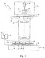
- FIG. 1shows a microlithographic projection exposure apparatus, denoted in its entirety by 10 , in a longitudinal section.
- the projection exposure apparatus 10comprises an illumination system 12 for generating a projection light beam 13 , which includes a projection light source 14 , illumination optics indicated by 16 and a diaphragm 18 .
- the projection exposure apparatus 10furthermore comprises a projection objective 20 which projects a reduced image of a mask 24 , arranged in its object plane 22 , onto a photosensitive surface 26 arranged in an image plane 28 of the projection objective 20 .
- the projection objective 20contains a multiplicity of optical components, only some of which (not dealt with in detail) are represented by way of example in FIG. 1 .
- the photosensitive surface 26may, for example, be a photoresist which is applied on a support 30 , for example a silicon wafer.
- the supportis fastened on the bottom of an open-topped container 32 with the shape of a trough, which can be displaced parallel to the image plane by a first displacement device denoted by 36 .
- the container 32is filled sufficiently high with an immersion liquid 38 so that an interspace 40 between the photosensitive surface 26 and an end face 42 of the projection objective 20 is filled completely with the immersion liquid 38 .
- the container 32also contains a temperature regulating device 44 , which may include a heating device or alternatively a combined heating/cooling device.
- a temperature sensor 46which records the temperature of the immersion liquid 38 very accurately, is fastened on the inside of the container 32 .
- the temperature regulating device 44 and the temperature sensor 46are connected, via lines which do not impede the displacement of the container 32 , to a temperature controller 48 which has a slide switch 50 for adjusting a setpoint temperature.
- the reticle 24whose structures are intended to be projected onto the photosensitive surface 26 , can be displaced in the object plane 22 by using a second displacement device 52 , so that images of the entire structured region of the reticle 24 can progressively be formed on the photosensitive surface 26 .
- the projection exposure apparatus 10functions in the following way:
- the projection light beam 13 generated by the illumination device 12passes through the structures of the reticle 24 and enters the projection objective 20 .
- the latterforms a reduced image of the structures through which the projection light beam 13 has passed.
- the reticle 24may be illuminated in a “step and scan” process. In this case, the entire region of the reticle 24 is illuminated by scanning while the second displacement device 52 moves the reticle 24 through the projection light beam delimited by the diaphragm 18 .
- the container 32 with the support 30 fastened in itis subjected to a movement (usually in the opposite direction) by using the first displacement device 36 , the displacement speed of which is reduced relative to that of the reticle 24 by the reduction ratio of the projection objective 20 .
- the end face 42 of the projection objective 20is moved through the immersion liquid 38 carried along by the container 32 , which leads to mixing of the immersion liquid 38 .
- Such mixingis desirable since the immersion liquid 38 may become locally heated by the projection light passing through, so that the temperature sensor 46 might otherwise possibly not measure the temperature actually prevailing in the interspace 40 .
- additional mixing devicesmay of course be arranged in the container 32 . It is likewise possible to fit the container 32 in a liquid circuit, as is known per se in the prior art.
- the temperature regulating device 44 and the temperature sensor 46may then be integrated in this temperature circuit alongside a filter which may optionally be provided.
- the setpoint temperature of the temperature controller 48is changed by actuating the slide switch 50 and the exposure is repeated.
- Changing the temperature of the immersion liquid 38changes its refractive index.
- the further exposure of photosensitive surfaces 26is then carried out at this finally adjusted temperature of the immersion liquid 38 .
- FIG. 2shows an enlarged detail of FIG. 1 , in which a ray path is indicated in the region of the interspace 40 between the end face 42 of the projection objective 20 and the photosensitive surface 26 .
- the end face 42 of the projection objective 20includes a flush-fitted planoconvex terminating lens 52 which constitutes the last optical component of the projection optics (merely indicated by 54 ) of the projection objective 20 .
- FIG. 2indicates a plurality of projection light rays 56 , 58 , 60 which propagate through the preceding optical components of the projection objective 20 towards the terminating lens 52 .
- the representationis highly schematised and not true to scale in order to show the effect of the temperature on the imaging properties of the projection objective 20 more clearly.
- the projection objective 20 shown in FIG. 2produces an image distorted by spherical aberration.
- the focal planes of the near-axis projection light rays 56lies in the plane of the photosensitive surface 26
- the focal planes of the off-axial projection light rays 58 and 60lie in the interspace 40 .
- the distance of the focal planes from the photosensitive surface 26in this case increases commensurately when the projection light rays 56 , 58 , 60 pass through the terminating lens 52 further away from the optical axis denoted by 62 .
- FIG. 3shows the detail in FIG. 2 after the temperature of the immersion liquid 38 has been raised.
- the immersion liquidnow has a higher refractive index than in the state shown in FIG. 2 .
- the effect of thisis that the projection light rays 56 , 58 , 60 are refracted more strongly at the interface between the terminating lens 52 and the immersion liquid 38 .
- This stronger refractionhas a commensurately greater effect the further the projection light rays are away from the optical axis 62 , since the off-axial projection light rays pass through this interface at a larger angle.
- the focal length of the projection objective 20is extended for the off-axial rays so that, in the ideal case with a correspondingly selected temperature, the focal planes of all the projection light rays 56 , 58 , 60 coincide with the image plane in 28 which the photosensitive surface 26 is arranged.
- FIG. 4shows an enlarged detail, corresponding to FIG. 2 , of a projection exposure apparatus having a different projection objective 120 .
- parts modified with respect to FIG. 2are denoted by reference numerals that are increased by 100 .
- the projection optics 154 of the projection objective 120do not have an inherent spherical aberration.
- the projection light rays 156 , 158 , 160therefore meet at a focal point.
- this focal pointdoes not lie in the image plane 28 , i.e. the projection objective 120 has a focusing error.
- Such a focusing errorcould, for example, be remedied by slightly displacing the support 30 with the photosensitive surface 26 in the direction of the optical axis 62 with the use of a suitable displacement device.
- the accuracy required for thiscan be achieved only with great technical outlay when mechanical displacement devices are used.
- FIG. 6shows details of another exemplary embodiment with a projection exposure apparatus denoted in its entirety by 210 , in a representation similar to FIG. 1 .
- parts modified with respect to the embodiment shown in FIG. 1are provided with reference numerals increased by 200 .
- FIG. 6shows the projection exposure apparatus 210 in an adjustment mode, in which the support 30 is replaced by a sensor device 64 .
- the sensor device 64may, for example, be a CCD sensor, as it is known per se in the art.
- the photosensitive surface 66 of the sensor device 64is arranged in the image plane 28 of the projection objective 20 .
- the sensor device 64records exactly the same image as the one to which the photosensitive surface 26 is exposed during the normal projection mode.
- the projectionis in this case carried out using a special test reticle 70 , which is arranged in place of the normal reticle 24 in the object plane 22 of the projection objective 20 .
- the projection exposure apparatus 210furthermore has a computer unit 68 which is connected to a temperature controller 248 for the temperature regulating device 44 .
- the projection exposure apparatus 210functions in the following way:
- an image of the structures contained on the test reticle 70is formed on the photosensitive surface 66 of the sensor device 64 by the projection objective 20 .
- This imageis recorded by the sensor device 64 and transmitted in digital form to the computer unit 68 .
- the latterdetermines a setpoint temperature which is sent to the temperature controller 248 .
- the temperature controller 248then ensures that the immersion liquid 38 is brought to this new setpoint temperature.
- the sensor device 64records the image of the structures of the test reticle 70 as modified by the temperature change, and likewise feeds these data to the computer unit 68 .
- the computer unit 68establishes whether the temperature change has led to an improvement or deterioration in the imaging properties of the projection objective 120 .
- the setpoint temperatureis changed again in accordance with this result. This recursive process is continued until it is no longer possible to improve the imaging properties of the projection objective by changing the temperature.
Landscapes
- Physics & Mathematics (AREA)
- General Physics & Mathematics (AREA)
- Health & Medical Sciences (AREA)
- Life Sciences & Earth Sciences (AREA)
- Atmospheric Sciences (AREA)
- Toxicology (AREA)
- Engineering & Computer Science (AREA)
- Environmental & Geological Engineering (AREA)
- Epidemiology (AREA)
- Public Health (AREA)
- Exposure Of Semiconductors, Excluding Electron Or Ion Beam Exposure (AREA)
- Exposure And Positioning Against Photoresist Photosensitive Materials (AREA)
Abstract
Description
- This is a continuation application of international application PCT/EP2003/001564, filed Feb. 17, 2003, which claims priority of German patent application DE 102 57 766.8, filed Dec. 10, 2002. The fill disclosure of both earlier applications is incorporated herein by reference.
- 1. Field of the Invention
- The invention generally relates to microlithographic projection exposure apparatuses as are used in the manufacture of integrated circuits and other microstructured devices. More particularly, the invention relates to a method for improving an optical imaging property, for example spherical aberration or the focal length, of a projection objective of such an apparatus. The invention further relates to a microlithographic projection exposure apparatus as such.
- 2. Description of Related Art
- It is known to change the spatial position of individual optical components, for example by using manipulators, in a projection objective of a microlithographic projection exposure apparatus in order to improve the imaging properties of the objective. The positional change of the relevant optical components is in this case carried out on the projection objective once it has finally been installed, and in general before it has yet been put into operation for the first time. This type of fine adjustment may nevertheless be carried out at a later time, for example in order to compensate for deteriorations of the imaging properties due to ageing. A procedure often adopted in these methods is to record one or more imaging properties of the projection objective by using a sensor arranged in its image plane. The way in which positional changes of individual optical components affect the imaging properties is then observed. The optical imaging properties of the projection objective can thus be optimised by adjusting the optical components.
- From EP 0 023 231 B1 a microlithographic projection exposure apparatus is known that has, in order to hold a support for a semiconductor wafer to be exposed, an open-topped container whose upper edge is higher than the lower delimiting surface of the projection objective. The container is provided with feed and discharge lines for an immersion liquid, which is circulated in a liquid circuit. When the projection exposure apparatus is in operation, the immersion liquid fills the interspace which is left between the semiconductor wafer to be exposed and a boundary surface of the projection exposure objective, which faces it. The resolving power of the projection objective is increased because the refractive index of the immersion liquid is higher than that of air.
- The known projection exposure apparatus furthermore has a device for regulating the temperature of the immersion liquid, which is arranged in the liquid circuit. The temperature of the semiconductor wafer to be exposed can thereby be kept constant, so as to avoid imaging errors due to thermally induced movements of the semiconductor wafer.
- The use of immersion liquids in microlithographic projection exposure apparatus is also known from JP 10-303 114 A. This addresses the problem that undesirable temperature fluctuations of the immersion liquid can also cause a deterioration of the imaging properties of the projection objective. The reason for this involves the dependency of the refractive index of the immersion liquid on the temperature. In order to resolve this problem, various measures are proposed by which the temperature of the immersion liquid can be kept constant within narrow limits during operation of the projection exposure apparatus.
- It is an object of the present invention to provide a method and a microlithographic projection exposure apparatus of the type, in which the optical imaging properties of a projection objective can be improved even more easily and effectively once it has finally been installed.
- This object is achieved, with a projection objective which is part of a microlithographic projection exposure apparatus for projecting a reticle, arranged in an object plane of the projection objective, onto a photosensitive surface that is arranged in an image plane of the projection objective, by a method comprising the following steps:
- a) introducing an immersion liquid into an interspace between the photosensitive surface and an end face of the projection objective, which faces the photosensitive surface;
- b) determining an imaging property of the projection objective;
- c) comparing the imaging property determined in step b) with a target imaging property;
- d) changing the temperature of the immersion liquid until the imaging property as determined in step b) is as close as possible to the target imaging property.
- In order to improve the optical imaging properties of the projection objective, use is made of the discovery that the immersion liquid constitutes an optical component of the projection exposure apparatus, which in principle influences its optical properties just as much as, for instance, the lenses arranged in the projection objective. Instead of now adjusting (exclusively) the lenses or other optical components inside the projection objective mechanically in the optical path of the projection objective, the invention exploits the possibility of influencing the refractive index of the “immersion liquid” optical component via its temperature.
- Although in principle it is also possible to change the refractive index of the optical components contained in the projection objective via the temperature, a temperature change is very much more difficult to achieve there since the materials used for lenses and the like have a low thermal conductivity, which makes it considerably harder to set a homogeneous temperature distribution throughout the optically active volume. Conversely, the temperature of the immersion liquid can quite easily be brought to a predeterminable value and kept constant over the corresponding optically active region, for example by circulating the liquid.
- Since the refractive index of many liquids suitable as an immersion liquid depends only very weakly and—within small temperature intervals—approximately linearly on the temperature, the refractive index of the immersion liquid can be set very precisely via the temperature. With a projection exposure apparatus designed for a wavelength of 193 nm, for example, in which the interspace between the photosensitive surface and the end face of the projection objective is filled with a 1 mm thick layer of water, the refractive index n=1.45 can be varied by one hundredth of a part per thousand by raising or lowering the temperature by 50 mK.
- In order to determine the imaging property, it is in theory possible to position an additional optical system in the image plane of the projection objective, so that an image generated by the projection objective can be observed directly on a screen or through an eyepiece. More simply, the imaging property may be determined by projecting a test reticle through the projection objective and the immersion liquid onto a photosensitive element arranged in the image plane. The imaging properties can then be determined reproducibly and quantifiably by using instruments, which are known per se, to analyse the image stored on the photosensitive element. For example, a photoemulsion may be envisaged as the photosensitive element.
- It is nevertheless particularly advantageous for the photosensitive element to be a sensor device, in particular a CCD sensor. In this way, the image generated in the image plane can be directly recorded and evaluated, i.e. without developing a photoemulsion or the like, in order to determine the imaging properties.
- As an alternative to this, the imaging property may also be determined by using an interferometer as known, for example, from WO 01/632 33 A1.
- By using the method according to the invention, it is possible to improve all optical imaging properties of the projection objective which can be influenced by the immersion liquid. For example, the optical imaging property to be improved may be a spherical aberration caused by the projection objective. Such spherical aberrations occur particularly in projection objectives with a high numerical aperture.
- The optical imaging property to be improved may also, for example, be the focal length of the projection objective. Since very accurate arrangement of the reticle in the focal plane of the projection objective is necessary so that a high-resolution image of the structures to be projected—which are contained in this reticle—can be formed on the photosensitive surface, conventional types of projection exposure apparatus often have an adjustment feature with which the support of the photosensitive surface can be moved along the optical axis of the projection objective. In this way, it is possible to position the photosensitive surface in the focal plane of the projection objective. These mechanical adjustment devices, however, have quite elaborate designs. By changing the temperature of the immersion liquid, it is very easy to influence the focal length of the projection objective so that an adjustment feature for the support of the photosensitive surface may be obviated.
- If a projection exposure apparatus comprises a sensor device—in particular a CCD sensor—which can be arranged in the image plane of the projection objective, a temperature control device for setting a target temperature of the immersion liquid, and a computer unit which is connected to the temperature control device, the latter may be used to determine the target temperature of the immersion liquid from signals generated by the sensor device.
- Such a projection exposure apparatus allows automated improvement of the optical imaging properties of the projection objective by changing the temperature of the immersion liquid. The computer unit may, for example, be designed so that it determines the imaging properties of the projection objective from the signals generated by the sensor device, and compares them with a target imaging property. In a control process, the computer unit then causes the temperature management device to change the temperature of the immersion liquid until the imaging property as recorded by the sensor device is as close as possible to the target imaging property. Such a projection exposure apparatus allows an operator to compensate automatically for certain deteriorations of the imaging properties of the projection objective, i.e. without drawing in specialists, by changing the refractive index of the immersion liquid. Possible causes of the deteriorations may, for example, be ageing-induced material modifications or fluctuations in the air pressure.
- Various features and advantages of the present invention may be more readily understood with reference to the following detailed description taken in conjunction with the accompanying drawing in which:
FIG. 1 is a simplified representation of a microlithographic projection exposure apparatus in a longitudinal section;FIG. 2 shows an enlarged detail ofFIG. 1 , in which ray paths in the region of an immersion liquid are indicated;FIG. 3 shows the detail according toFIG. 2 , but after raising the temperature of the immersion liquid;FIG. 4 shows an enlarged detail, corresponding toFIG. 2 , of a projection exposure apparatus having different imaging optics;FIG. 5 shows the detail according toFIG. 4 , but after raising the temperature of the immersion liquid;FIG. 6 shows a simplified representation of another microlithographic projection exposure apparatus, having a sensor device arranged in the image plane, in a longitudinal section.FIG. 1 shows a microlithographic projection exposure apparatus, denoted in its entirety by10, in a longitudinal section. Theprojection exposure apparatus 10 comprises anillumination system 12 for generating aprojection light beam 13, which includes aprojection light source 14, illumination optics indicated by16 and adiaphragm 18.- The
projection exposure apparatus 10 furthermore comprises aprojection objective 20 which projects a reduced image of amask 24, arranged in itsobject plane 22, onto aphotosensitive surface 26 arranged in animage plane 28 of theprojection objective 20. Theprojection objective 20 contains a multiplicity of optical components, only some of which (not dealt with in detail) are represented by way of example inFIG. 1 . - The
photosensitive surface 26 may, for example, be a photoresist which is applied on asupport 30, for example a silicon wafer. The support is fastened on the bottom of an open-toppedcontainer 32 with the shape of a trough, which can be displaced parallel to the image plane by a first displacement device denoted by36. Thecontainer 32 is filled sufficiently high with animmersion liquid 38 so that aninterspace 40 between thephotosensitive surface 26 and anend face 42 of theprojection objective 20 is filled completely with theimmersion liquid 38. - The
container 32 also contains atemperature regulating device 44, which may include a heating device or alternatively a combined heating/cooling device. Atemperature sensor 46, which records the temperature of theimmersion liquid 38 very accurately, is fastened on the inside of thecontainer 32. - The
temperature regulating device 44 and thetemperature sensor 46 are connected, via lines which do not impede the displacement of thecontainer 32, to atemperature controller 48 which has aslide switch 50 for adjusting a setpoint temperature. - The
reticle 24, whose structures are intended to be projected onto thephotosensitive surface 26, can be displaced in theobject plane 22 by using asecond displacement device 52, so that images of the entire structured region of thereticle 24 can progressively be formed on thephotosensitive surface 26. - The
projection exposure apparatus 10 functions in the following way: - The
projection light beam 13 generated by theillumination device 12 passes through the structures of thereticle 24 and enters theprojection objective 20. On thephotosensitive surface 26, the latter forms a reduced image of the structures through which theprojection light beam 13 has passed. In order to project the entire area of thereticle 24 onto thephotosensitive surface 26, thereticle 24 may be illuminated in a “step and scan” process. In this case, the entire region of thereticle 24 is illuminated by scanning while thesecond displacement device 52 moves thereticle 24 through the projection light beam delimited by thediaphragm 18. During this scanning movement, thecontainer 32 with thesupport 30 fastened in it is subjected to a movement (usually in the opposite direction) by using thefirst displacement device 36, the displacement speed of which is reduced relative to that of thereticle 24 by the reduction ratio of theprojection objective 20. - During this displacement of the
container 32, theend face 42 of theprojection objective 20 is moved through theimmersion liquid 38 carried along by thecontainer 32, which leads to mixing of theimmersion liquid 38. Such mixing is desirable since theimmersion liquid 38 may become locally heated by the projection light passing through, so that thetemperature sensor 46 might otherwise possibly not measure the temperature actually prevailing in theinterspace 40. If the mixing due to the displacement of thecontainer 32 is not sufficient, additional mixing devices may of course be arranged in thecontainer 32. It is likewise possible to fit thecontainer 32 in a liquid circuit, as is known per se in the prior art. Thetemperature regulating device 44 and thetemperature sensor 46 may then be integrated in this temperature circuit alongside a filter which may optionally be provided. - If it is found during a test process when adjusting the projection objective, or during subsequent operation by checking the wafers which are produced, that the imaging properties of the
projection objective 20 do not correspond to an intended target imaging property, for example because the imaging on thephotosensitive surface 26 is distorted by spherical aberration, then the setpoint temperature of thetemperature controller 48 is changed by actuating theslide switch 50 and the exposure is repeated. Changing the temperature of theimmersion liquid 38 changes its refractive index. The dependency of the refractive index on the temperature—at least in small temperature intervals—is approximately linear formany immersion liquids 38, so that a temperature at which one or more imaging properties of theprojection objective 20 are improved can be determined very straightforwardly for theimmersion liquid 38 in a recursive process. The further exposure ofphotosensitive surfaces 26 is then carried out at this finally adjusted temperature of theimmersion liquid 38. - The effect of the refractive index of the
immersion liquid 38 on the imaging properties of theprojection objective 20 will be explained in more detail below with reference to FIGS.2 to5. FIG. 2 shows an enlarged detail ofFIG. 1 , in which a ray path is indicated in the region of theinterspace 40 between theend face 42 of theprojection objective 20 and thephotosensitive surface 26. In this exemplary embodiment, theend face 42 of theprojection objective 20 includes a flush-fittedplanoconvex terminating lens 52 which constitutes the last optical component of the projection optics (merely indicated by54) of theprojection objective 20. For illustrative purposes,FIG. 2 indicates a plurality of projection light rays56,58,60 which propagate through the preceding optical components of theprojection objective 20 towards the terminatinglens 52. The representation is highly schematised and not true to scale in order to show the effect of the temperature on the imaging properties of theprojection objective 20 more clearly.- The
projection objective 20 shown inFIG. 2 produces an image distorted by spherical aberration. This means that the focal lengths are respectively different for the near-axis projection light rays56 and for the off-axial projection light beams58 and60. InFIG. 2 , only the focal plane of the near-axis projection light rays56 lies in the plane of thephotosensitive surface 26, whereas the focal planes of the off-axial projection light rays58 and60 lie in theinterspace 40. The distance of the focal planes from thephotosensitive surface 26 in this case increases commensurately when the projection light rays56,58,60 pass through the terminatinglens 52 further away from the optical axis denoted by62. FIG. 3 shows the detail inFIG. 2 after the temperature of theimmersion liquid 38 has been raised. The immersion liquid now has a higher refractive index than in the state shown inFIG. 2 . The effect of this is that the projection light rays56,58,60 are refracted more strongly at the interface between the terminatinglens 52 and theimmersion liquid 38. This stronger refraction has a commensurately greater effect the further the projection light rays are away from theoptical axis 62, since the off-axial projection light rays pass through this interface at a larger angle. The result of this is that the focal length of theprojection objective 20 is extended for the off-axial rays so that, in the ideal case with a correspondingly selected temperature, the focal planes of all the projection light rays56,58,60 coincide with the image plane in28 which thephotosensitive surface 26 is arranged.- By changing the temperature of the
immersion liquid 38, it is thus possible to compensate retrospectively for an inherent spherical aberration in theprojection objective 20. FIG. 4 shows an enlarged detail, corresponding toFIG. 2 , of a projection exposure apparatus having adifferent projection objective 120. In this embodiment, parts modified with respect toFIG. 2 are denoted by reference numerals that are increased by100.- Unlike the
projection optics 54 shown inFIGS. 2 and 3 , theprojection optics 154 of theprojection objective 120 do not have an inherent spherical aberration. The projection light rays156,158,160 therefore meet at a focal point. As can be seen inFIG. 4 , however, this focal point does not lie in theimage plane 28, i.e. theprojection objective 120 has a focusing error. Such a focusing error could, for example, be remedied by slightly displacing thesupport 30 with thephotosensitive surface 26 in the direction of theoptical axis 62 with the use of a suitable displacement device. Unfortunately, the accuracy required for this can be achieved only with great technical outlay when mechanical displacement devices are used. - As shown by
FIG. 5 , it is likewise possible to extend the focal length of theprojection objective 120 deliberately by raising the temperature of theimmersion liquid 38. Admittedly, this does introduce a spherical aberration (not represented inFIG. 5 ). Nevertheless, the effects of such a spherical aberration may be so small that they are negligible in view of the optimisation of the focal length of the projection objective, or they can be compensated for by other measures. FIG. 6 shows details of another exemplary embodiment with a projection exposure apparatus denoted in its entirety by210, in a representation similar toFIG. 1 . Here again, parts modified with respect to the embodiment shown inFIG. 1 are provided with reference numerals increased by200.FIG. 6 shows theprojection exposure apparatus 210 in an adjustment mode, in which thesupport 30 is replaced by asensor device 64. Thesensor device 64 may, for example, be a CCD sensor, as it is known per se in the art. In the adjustment mode, thephotosensitive surface 66 of thesensor device 64 is arranged in theimage plane 28 of theprojection objective 20. In this way, thesensor device 64 records exactly the same image as the one to which thephotosensitive surface 26 is exposed during the normal projection mode. The projection is in this case carried out using a special test reticle70, which is arranged in place of thenormal reticle 24 in theobject plane 22 of theprojection objective 20.- Instead of the CCD sensor, it is also possible to use an interferometer as the sensor device in a manner which is known per se. Wavefronts in pupil planes can thereby be recorded. This is described in more detail in the aforementioned WO 01/63233 A1.
- In contrast to the
projection exposure apparatus 10 inFIG. 1 , theprojection exposure apparatus 210 furthermore has acomputer unit 68 which is connected to atemperature controller 248 for thetemperature regulating device 44. In the adjustment mode, theprojection exposure apparatus 210 functions in the following way: - First, an image of the structures contained on the test reticle70 is formed on the
photosensitive surface 66 of thesensor device 64 by theprojection objective 20. This image is recorded by thesensor device 64 and transmitted in digital form to thecomputer unit 68. From the data received, the latter determines a setpoint temperature which is sent to thetemperature controller 248. Thetemperature controller 248 then ensures that theimmersion liquid 38 is brought to this new setpoint temperature. Thesensor device 64 records the image of the structures of the test reticle70 as modified by the temperature change, and likewise feeds these data to thecomputer unit 68. By using algorithms which are known per se, thecomputer unit 68 establishes whether the temperature change has led to an improvement or deterioration in the imaging properties of theprojection objective 120. The setpoint temperature is changed again in accordance with this result. This recursive process is continued until it is no longer possible to improve the imaging properties of the projection objective by changing the temperature.
Claims (11)
Priority Applications (3)
| Application Number | Priority Date | Filing Date | Title |
|---|---|---|---|
| US11/739,192US20070195299A1 (en) | 2002-12-10 | 2007-04-24 | Method for improving an Optical Imaging Property of a Projection Objective of a Microlithographic Projection Exposure Apparatus |
| US12/203,738US8237915B2 (en) | 2002-12-10 | 2008-09-03 | Method for improving an optical imaging property of a projection objective of a microlithographic projection exposure apparatus |
| US13/564,857US20130114056A1 (en) | 2002-12-10 | 2012-08-02 | Method for improving an optical imaging property of a projection objective of a microlithographic projection exposure apparatus |
Applications Claiming Priority (3)
| Application Number | Priority Date | Filing Date | Title |
|---|---|---|---|
| DE10257766ADE10257766A1 (en) | 2002-12-10 | 2002-12-10 | Method for setting a desired optical property of a projection lens and microlithographic projection exposure system |
| DE10257766.8 | 2002-12-10 | ||
| PCT/EP2003/001564WO2004053596A2 (en) | 2002-12-10 | 2003-02-17 | Method for adjusting a desired optical property of a positioning lens and microlithographic projection exposure system |
Related Parent Applications (2)
| Application Number | Title | Priority Date | Filing Date |
|---|---|---|---|
| PCT/EP2003/001564Continuation-In-PartWO2004053596A2 (en) | 2002-12-10 | 2003-02-17 | Method for adjusting a desired optical property of a positioning lens and microlithographic projection exposure system |
| PCT/EP2003/001564ContinuationWO2004053596A2 (en) | 2002-12-10 | 2003-02-17 | Method for adjusting a desired optical property of a positioning lens and microlithographic projection exposure system |
Related Child Applications (1)
| Application Number | Title | Priority Date | Filing Date |
|---|---|---|---|
| US11/739,192ContinuationUS20070195299A1 (en) | 2002-12-10 | 2007-04-24 | Method for improving an Optical Imaging Property of a Projection Objective of a Microlithographic Projection Exposure Apparatus |
Publications (2)
| Publication Number | Publication Date |
|---|---|
| US20050264780A1true US20050264780A1 (en) | 2005-12-01 |
| US7227616B2 US7227616B2 (en) | 2007-06-05 |
Family
ID=32477537
Family Applications (4)
| Application Number | Title | Priority Date | Filing Date |
|---|---|---|---|
| US11/149,568Expired - Fee RelatedUS7227616B2 (en) | 2002-12-10 | 2005-06-10 | Method for improving an optical imaging property of a projection objective of a microlithographic projection exposure apparatus |
| US11/739,192AbandonedUS20070195299A1 (en) | 2002-12-10 | 2007-04-24 | Method for improving an Optical Imaging Property of a Projection Objective of a Microlithographic Projection Exposure Apparatus |
| US12/203,738Expired - Fee RelatedUS8237915B2 (en) | 2002-12-10 | 2008-09-03 | Method for improving an optical imaging property of a projection objective of a microlithographic projection exposure apparatus |
| US13/564,857AbandonedUS20130114056A1 (en) | 2002-12-10 | 2012-08-02 | Method for improving an optical imaging property of a projection objective of a microlithographic projection exposure apparatus |
Family Applications After (3)
| Application Number | Title | Priority Date | Filing Date |
|---|---|---|---|
| US11/739,192AbandonedUS20070195299A1 (en) | 2002-12-10 | 2007-04-24 | Method for improving an Optical Imaging Property of a Projection Objective of a Microlithographic Projection Exposure Apparatus |
| US12/203,738Expired - Fee RelatedUS8237915B2 (en) | 2002-12-10 | 2008-09-03 | Method for improving an optical imaging property of a projection objective of a microlithographic projection exposure apparatus |
| US13/564,857AbandonedUS20130114056A1 (en) | 2002-12-10 | 2012-08-02 | Method for improving an optical imaging property of a projection objective of a microlithographic projection exposure apparatus |
Country Status (6)
| Country | Link |
|---|---|
| US (4) | US7227616B2 (en) |
| EP (1) | EP1570315B1 (en) |
| JP (1) | JP2006509357A (en) |
| AU (1) | AU2003221481A1 (en) |
| DE (2) | DE10257766A1 (en) |
| WO (1) | WO2004053596A2 (en) |
Cited By (18)
| Publication number | Priority date | Publication date | Assignee | Title |
|---|---|---|---|---|
| US20050174550A1 (en)* | 2003-10-15 | 2005-08-11 | Asml Netherlands B.V. | Lithographic apparatus and device manufacturing method |
| US20060082741A1 (en)* | 2004-10-18 | 2006-04-20 | Asml Netherlands B.V. | Lithographic apparatus and device manufacturing method |
| US20060221317A1 (en)* | 2003-09-25 | 2006-10-05 | Martin Niehoff | Immersion lithography method and device for illuminating a substrate |
| US20070070316A1 (en)* | 2004-01-20 | 2007-03-29 | Albrecht Ehrmann | Microlithographic projection exposure apparatus and measuring device for a projection lens |
| US20070211233A1 (en)* | 2006-03-13 | 2007-09-13 | Asml Netherlands B.V. | Lithographic apparatus, control system and device manufacturing method |
| US20070258070A1 (en)* | 2004-07-12 | 2007-11-08 | Nikon Corporation | Method for Determining Exposure Condition, Exposure Method, Exposure Apparatus, and Method for Manufacturing Device |
| US20080084546A1 (en)* | 2004-08-03 | 2008-04-10 | Nikon Corporation | Exposure Apparatus,Exposure Method, And For Producing Device |
| US20080106707A1 (en)* | 2004-02-04 | 2008-05-08 | Nikon Corporation | Exposure Apparatus, Exposure Method, and Method for Producing Device |
| US20080106711A1 (en)* | 2004-11-18 | 2008-05-08 | Carl Zeiss Smt Ag | Projection Lens System of a Microlithographic Projection Exposure Installation |
| US20080278695A1 (en)* | 2005-12-06 | 2008-11-13 | Nikon Corporation | Exposing method, exposure apparatus, and device fabricating method |
| US20090001403A1 (en)* | 2007-06-29 | 2009-01-01 | Motorola, Inc. | Inductively excited quantum dot light emitting device |
| US20090054752A1 (en)* | 2007-08-22 | 2009-02-26 | Motorola, Inc. | Method and apparatus for photoplethysmographic sensing |
| US20090115977A1 (en)* | 2005-04-18 | 2009-05-07 | Nikon Corporation | Exposure Apparatus, Exposure Method, and Device Manufacturing Method |
| US8363206B2 (en) | 2006-05-09 | 2013-01-29 | Carl Zeiss Smt Gmbh | Optical imaging device with thermal attenuation |
| US8570486B2 (en) | 2003-10-15 | 2013-10-29 | Asml Netherlands B.V. | Lithographic apparatus and device manufacturing method |
| US20130293854A1 (en)* | 2012-05-01 | 2013-11-07 | Canon Kabushiki Kaisha | Exposure apparatus and device fabrication method |
| US8913223B2 (en) | 2003-07-16 | 2014-12-16 | Asml Netherlands B.V. | Lithographic apparatus and device manufacturing method |
| US9025126B2 (en) | 2007-07-31 | 2015-05-05 | Nikon Corporation | Exposure apparatus adjusting method, exposure apparatus, and device fabricating method |
Families Citing this family (159)
| Publication number | Priority date | Publication date | Assignee | Title |
|---|---|---|---|---|
| CN101470360B (en) | 2002-11-12 | 2013-07-24 | Asml荷兰有限公司 | Immersion lithographic apparatus and device manufacturing method |
| US7372541B2 (en) | 2002-11-12 | 2008-05-13 | Asml Netherlands B.V. | Lithographic apparatus and device manufacturing method |
| DE60335595D1 (en) | 2002-11-12 | 2011-02-17 | Asml Netherlands Bv | Immersion lithographic apparatus and method of making a device |
| KR100585476B1 (en) | 2002-11-12 | 2006-06-07 | 에이에스엠엘 네델란즈 비.브이. | Lithographic Apparatus and Device Manufacturing Method |
| US10503084B2 (en) | 2002-11-12 | 2019-12-10 | Asml Netherlands B.V. | Lithographic apparatus and device manufacturing method |
| US9482966B2 (en) | 2002-11-12 | 2016-11-01 | Asml Netherlands B.V. | Lithographic apparatus and device manufacturing method |
| SG121822A1 (en) | 2002-11-12 | 2006-05-26 | Asml Netherlands Bv | Lithographic apparatus and device manufacturing method |
| CN100568101C (en) | 2002-11-12 | 2009-12-09 | Asml荷兰有限公司 | Photolithography apparatus and device manufacturing method |
| US7110081B2 (en) | 2002-11-12 | 2006-09-19 | Asml Netherlands B.V. | Lithographic apparatus and device manufacturing method |
| SG131766A1 (en) | 2002-11-18 | 2007-05-28 | Asml Netherlands Bv | Lithographic apparatus and device manufacturing method |
| SG121829A1 (en) | 2002-11-29 | 2006-05-26 | Asml Netherlands Bv | Lithographic apparatus and device manufacturing method |
| US7242455B2 (en) | 2002-12-10 | 2007-07-10 | Nikon Corporation | Exposure apparatus and method for producing device |
| WO2004053955A1 (en)* | 2002-12-10 | 2004-06-24 | Nikon Corporation | Exposure system and device producing method |
| DE10257766A1 (en)* | 2002-12-10 | 2004-07-15 | Carl Zeiss Smt Ag | Method for setting a desired optical property of a projection lens and microlithographic projection exposure system |
| DE10261775A1 (en) | 2002-12-20 | 2004-07-01 | Carl Zeiss Smt Ag | Device for the optical measurement of an imaging system |
| EP2466623B1 (en) | 2003-02-26 | 2015-04-22 | Nikon Corporation | Exposure apparatus, exposure method, and method for producing device |
| KR101547077B1 (en) | 2003-04-09 | 2015-08-25 | 가부시키가이샤 니콘 | Exposure method and apparatus, and device manufacturing method |
| KR101225884B1 (en) | 2003-04-11 | 2013-01-28 | 가부시키가이샤 니콘 | Apparatus and method for maintaining immersion fluid in the gap under the projection lens during wafer exchange in an immersion lithography machine |
| TWI295414B (en) | 2003-05-13 | 2008-04-01 | Asml Netherlands Bv | Lithographic apparatus and device manufacturing method |
| KR101548832B1 (en)* | 2003-05-28 | 2015-09-01 | 가부시키가이샤 니콘 | Exposure method, exposure device, and device manufacturing method |
| TWI442694B (en) | 2003-05-30 | 2014-06-21 | Asml Netherlands Bv | Lithographic apparatus and device manufacturing method |
| US7213963B2 (en) | 2003-06-09 | 2007-05-08 | Asml Netherlands B.V. | Lithographic apparatus and device manufacturing method |
| US7317504B2 (en) | 2004-04-08 | 2008-01-08 | Asml Netherlands B.V. | Lithographic apparatus and device manufacturing method |
| EP2261741A3 (en) | 2003-06-11 | 2011-05-25 | ASML Netherlands B.V. | Lithographic apparatus and device manufacturing method |
| TW201721717A (en) | 2003-06-19 | 2017-06-16 | 尼康股份有限公司 | Exposure apparatus, exposure method, and device manufacturing method |
| US6867844B2 (en) | 2003-06-19 | 2005-03-15 | Asml Holding N.V. | Immersion photolithography system and method using microchannel nozzles |
| US6809794B1 (en) | 2003-06-27 | 2004-10-26 | Asml Holding N.V. | Immersion photolithography system and method using inverted wafer-projection optics interface |
| EP1498778A1 (en) | 2003-06-27 | 2005-01-19 | ASML Netherlands B.V. | Lithographic apparatus and device manufacturing method |
| EP1491956B1 (en) | 2003-06-27 | 2006-09-06 | ASML Netherlands B.V. | Lithographic apparatus and device manufacturing method |
| EP1494074A1 (en) | 2003-06-30 | 2005-01-05 | ASML Netherlands B.V. | Lithographic apparatus and device manufacturing method |
| EP1494075B1 (en) | 2003-06-30 | 2008-06-25 | ASML Netherlands B.V. | Lithographic projection apparatus and device manufacturing method |
| WO2005006418A1 (en) | 2003-07-09 | 2005-01-20 | Nikon Corporation | Exposure apparatus and method for manufacturing device |
| EP1500982A1 (en) | 2003-07-24 | 2005-01-26 | ASML Netherlands B.V. | Lithographic apparatus and device manufacturing method |
| WO2005010960A1 (en)* | 2003-07-25 | 2005-02-03 | Nikon Corporation | Inspection method and inspection device for projection optical system, and production method for projection optical system |
| EP1503244A1 (en) | 2003-07-28 | 2005-02-02 | ASML Netherlands B.V. | Lithographic projection apparatus and device manufacturing method |
| US7326522B2 (en) | 2004-02-11 | 2008-02-05 | Asml Netherlands B.V. | Device manufacturing method and a substrate |
| US7175968B2 (en) | 2003-07-28 | 2007-02-13 | Asml Netherlands B.V. | Lithographic apparatus, device manufacturing method and a substrate |
| US7779781B2 (en) | 2003-07-31 | 2010-08-24 | Asml Netherlands B.V. | Lithographic apparatus and device manufacturing method |
| US8149381B2 (en) | 2003-08-26 | 2012-04-03 | Nikon Corporation | Optical element and exposure apparatus |
| JP4474652B2 (en) | 2003-08-26 | 2010-06-09 | 株式会社ニコン | Optical element and exposure apparatus |
| US6954256B2 (en) | 2003-08-29 | 2005-10-11 | Asml Netherlands B.V. | Gradient immersion lithography |
| EP2261740B1 (en) | 2003-08-29 | 2014-07-09 | ASML Netherlands BV | Lithographic apparatus |
| TWI245163B (en) | 2003-08-29 | 2005-12-11 | Asml Netherlands Bv | Lithographic apparatus and device manufacturing method |
| TWI263859B (en) | 2003-08-29 | 2006-10-11 | Asml Netherlands Bv | Lithographic apparatus and device manufacturing method |
| EP1519231B1 (en) | 2003-09-29 | 2005-12-21 | ASML Netherlands B.V. | Lithographic apparatus and device manufacturing method |
| US7158211B2 (en) | 2003-09-29 | 2007-01-02 | Asml Netherlands B.V. | Lithographic apparatus and device manufacturing method |
| EP1519230A1 (en) | 2003-09-29 | 2005-03-30 | ASML Netherlands B.V. | Lithographic apparatus and device manufacturing method |
| US7352433B2 (en) | 2003-10-28 | 2008-04-01 | Asml Netherlands B.V. | Lithographic apparatus and device manufacturing method |
| US7411653B2 (en) | 2003-10-28 | 2008-08-12 | Asml Netherlands B.V. | Lithographic apparatus |
| TWI573175B (en) | 2003-10-28 | 2017-03-01 | 尼康股份有限公司 | Optical illumination device, exposure device, exposure method and device manufacturing method |
| US7528929B2 (en) | 2003-11-14 | 2009-05-05 | Asml Netherlands B.V. | Lithographic apparatus and device manufacturing method |
| TWI385414B (en) | 2003-11-20 | 2013-02-11 | 尼康股份有限公司 | Optical illuminating apparatus, illuminating method, exposure apparatus, exposure method and device fabricating method |
| US7545481B2 (en) | 2003-11-24 | 2009-06-09 | Asml Netherlands B.V. | Lithographic apparatus and device manufacturing method |
| US7460206B2 (en) | 2003-12-19 | 2008-12-02 | Carl Zeiss Smt Ag | Projection objective for immersion lithography |
| US7394521B2 (en) | 2003-12-23 | 2008-07-01 | Asml Netherlands B.V. | Lithographic apparatus and device manufacturing method |
| US7589818B2 (en) | 2003-12-23 | 2009-09-15 | Asml Netherlands B.V. | Lithographic apparatus, alignment apparatus, device manufacturing method, and a method of converting an apparatus |
| US7589822B2 (en) | 2004-02-02 | 2009-09-15 | Nikon Corporation | Stage drive method and stage unit, exposure apparatus, and device manufacturing method |
| TWI389174B (en) | 2004-02-06 | 2013-03-11 | 尼康股份有限公司 | Polarization changing device, optical illumination apparatus, light-exposure apparatus and light-exposure method |
| US7050146B2 (en) | 2004-02-09 | 2006-05-23 | Asml Netherlands B.V. | Lithographic apparatus and device manufacturing method |
| US7034917B2 (en) | 2004-04-01 | 2006-04-25 | Asml Netherlands B.V. | Lithographic apparatus, device manufacturing method and device manufactured thereby |
| US7227619B2 (en) | 2004-04-01 | 2007-06-05 | Asml Netherlands B.V. | Lithographic apparatus and device manufacturing method |
| US7295283B2 (en) | 2004-04-02 | 2007-11-13 | Asml Netherlands B.V. | Lithographic apparatus and device manufacturing method |
| US7898642B2 (en) | 2004-04-14 | 2011-03-01 | Asml Netherlands B.V. | Lithographic apparatus and device manufacturing method |
| US7379159B2 (en) | 2004-05-03 | 2008-05-27 | Asml Netherlands B.V. | Lithographic apparatus and device manufacturing method |
| US7616383B2 (en) | 2004-05-18 | 2009-11-10 | Asml Netherlands B.V. | Lithographic apparatus and device manufacturing method |
| US7486381B2 (en) | 2004-05-21 | 2009-02-03 | Asml Netherlands B.V. | Lithographic apparatus and device manufacturing method |
| US7481867B2 (en) | 2004-06-16 | 2009-01-27 | Edwards Limited | Vacuum system for immersion photolithography |
| US7463330B2 (en) | 2004-07-07 | 2008-12-09 | Asml Netherlands B.V. | Lithographic apparatus and device manufacturing method |
| US7161663B2 (en) | 2004-07-22 | 2007-01-09 | Asml Netherlands B.V. | Lithographic apparatus |
| US7304715B2 (en) | 2004-08-13 | 2007-12-04 | Asml Netherlands B.V. | Lithographic apparatus and device manufacturing method |
| US7701550B2 (en) | 2004-08-19 | 2010-04-20 | Asml Netherlands B.V. | Lithographic apparatus and device manufacturing method |
| US7133114B2 (en) | 2004-09-20 | 2006-11-07 | Asml Netherlands B.V. | Lithographic apparatus and device manufacturing method |
| US7522261B2 (en) | 2004-09-24 | 2009-04-21 | Asml Netherlands B.V. | Lithographic apparatus and device manufacturing method |
| US7355674B2 (en) | 2004-09-28 | 2008-04-08 | Asml Netherlands B.V. | Lithographic apparatus, device manufacturing method and computer program product |
| US7894040B2 (en) | 2004-10-05 | 2011-02-22 | Asml Netherlands B.V. | Lithographic apparatus and device manufacturing method |
| US7209213B2 (en) | 2004-10-07 | 2007-04-24 | Asml Netherlands B.V. | Lithographic apparatus and device manufacturing method |
| US7379155B2 (en) | 2004-10-18 | 2008-05-27 | Asml Netherlands B.V. | Lithographic apparatus and device manufacturing method |
| DE102004051357B4 (en)* | 2004-10-19 | 2013-08-22 | Carl Zeiss Microscopy Gmbh | Immersion microscope objective |
| US7414699B2 (en) | 2004-11-12 | 2008-08-19 | Asml Netherlands B.V. | Lithographic apparatus and device manufacturing method |
| US7583357B2 (en) | 2004-11-12 | 2009-09-01 | Asml Netherlands B.V. | Lithographic apparatus and device manufacturing method |
| US7251013B2 (en) | 2004-11-12 | 2007-07-31 | Asml Netherlands B.V. | Lithographic apparatus and device manufacturing method |
| US7423720B2 (en) | 2004-11-12 | 2008-09-09 | Asml Netherlands B.V. | Lithographic apparatus and device manufacturing method |
| US7411657B2 (en) | 2004-11-17 | 2008-08-12 | Asml Netherlands B.V. | Lithographic apparatus and device manufacturing method |
| US7145630B2 (en) | 2004-11-23 | 2006-12-05 | Asml Netherlands B.V. | Lithographic apparatus and device manufacturing method |
| US7161654B2 (en) | 2004-12-02 | 2007-01-09 | Asml Netherlands B.V. | Lithographic apparatus and device manufacturing method |
| US7446850B2 (en) | 2004-12-03 | 2008-11-04 | Asml Netherlands B.V. | Lithographic apparatus and device manufacturing method |
| US7397533B2 (en) | 2004-12-07 | 2008-07-08 | Asml Netherlands B.V. | Lithographic apparatus and device manufacturing method |
| US7248334B2 (en) | 2004-12-07 | 2007-07-24 | Asml Netherlands B.V. | Sensor shield |
| US7196770B2 (en) | 2004-12-07 | 2007-03-27 | Asml Netherlands B.V. | Prewetting of substrate before immersion exposure |
| US7365827B2 (en) | 2004-12-08 | 2008-04-29 | Asml Netherlands B.V. | Lithographic apparatus and device manufacturing method |
| US7352440B2 (en) | 2004-12-10 | 2008-04-01 | Asml Netherlands B.V. | Substrate placement in immersion lithography |
| US7403261B2 (en) | 2004-12-15 | 2008-07-22 | Asml Netherlands B.V. | Lithographic apparatus and device manufacturing method |
| US7528931B2 (en) | 2004-12-20 | 2009-05-05 | Asml Netherlands B.V. | Lithographic apparatus and device manufacturing method |
| US7880860B2 (en) | 2004-12-20 | 2011-02-01 | Asml Netherlands B.V. | Lithographic apparatus and device manufacturing method |
| US7405805B2 (en) | 2004-12-28 | 2008-07-29 | Asml Netherlands B.V. | Lithographic apparatus and device manufacturing method |
| US7491661B2 (en) | 2004-12-28 | 2009-02-17 | Asml Netherlands B.V. | Device manufacturing method, top coat material and substrate |
| US20060147821A1 (en) | 2004-12-30 | 2006-07-06 | Asml Netherlands B.V. | Lithographic apparatus and device manufacturing method |
| DE602006012746D1 (en) | 2005-01-14 | 2010-04-22 | Asml Netherlands Bv | Lithographic apparatus and manufacturing method |
| SG124351A1 (en) | 2005-01-14 | 2006-08-30 | Asml Netherlands Bv | Lithographic apparatus and device manufacturing method |
| KR101513840B1 (en) | 2005-01-31 | 2015-04-20 | 가부시키가이샤 니콘 | Exposure apparatus and method for manufacturing device |
| US8692973B2 (en) | 2005-01-31 | 2014-04-08 | Nikon Corporation | Exposure apparatus and method for producing device |
| KR20070095272A (en)* | 2005-01-31 | 2007-09-28 | 가부시키가이샤 니콘 | Exposure method, exposure apparatus and device manufacturing method |
| CN102360170B (en) | 2005-02-10 | 2014-03-12 | Asml荷兰有限公司 | Immersion liquid, exposure apparatus, and exposure process |
| US7378025B2 (en) | 2005-02-22 | 2008-05-27 | Asml Netherlands B.V. | Fluid filtration method, fluid filtered thereby, lithographic apparatus and device manufacturing method |
| US7224431B2 (en) | 2005-02-22 | 2007-05-29 | Asml Netherlands B.V. | Lithographic apparatus and device manufacturing method |
| US8018573B2 (en) | 2005-02-22 | 2011-09-13 | Asml Netherlands B.V. | Lithographic apparatus and device manufacturing method |
| US7428038B2 (en) | 2005-02-28 | 2008-09-23 | Asml Netherlands B.V. | Lithographic apparatus, device manufacturing method and apparatus for de-gassing a liquid |
| US7324185B2 (en) | 2005-03-04 | 2008-01-29 | Asml Netherlands B.V. | Lithographic apparatus and device manufacturing method |
| US7684010B2 (en) | 2005-03-09 | 2010-03-23 | Asml Netherlands B.V. | Lithographic apparatus, device manufacturing method, seal structure, method of removing an object and a method of sealing |
| US7330238B2 (en) | 2005-03-28 | 2008-02-12 | Asml Netherlands, B.V. | Lithographic apparatus, immersion projection apparatus and device manufacturing method |
| US7411654B2 (en) | 2005-04-05 | 2008-08-12 | Asml Netherlands B.V. | Lithographic apparatus and device manufacturing method |
| US7291850B2 (en) | 2005-04-08 | 2007-11-06 | Asml Netherlands B.V. | Lithographic apparatus and device manufacturing method |
| US20060232753A1 (en) | 2005-04-19 | 2006-10-19 | Asml Holding N.V. | Liquid immersion lithography system with tilted liquid flow |
| US7433016B2 (en) | 2005-05-03 | 2008-10-07 | Asml Netherlands B.V. | Lithographic apparatus and device manufacturing method |
| US7317507B2 (en) | 2005-05-03 | 2008-01-08 | Asml Netherlands B.V. | Lithographic apparatus and device manufacturing method |
| US8248577B2 (en) | 2005-05-03 | 2012-08-21 | Asml Netherlands B.V. | Lithographic apparatus and device manufacturing method |
| KR20180128526A (en) | 2005-05-12 | 2018-12-03 | 가부시키가이샤 니콘 | Projection optical system, exposure apparatus and device manufacturing method |
| US7652746B2 (en) | 2005-06-21 | 2010-01-26 | Asml Netherlands B.V. | Lithographic apparatus and device manufacturing method |
| US7751027B2 (en) | 2005-06-21 | 2010-07-06 | Asml Netherlands B.V. | Lithographic apparatus and device manufacturing method |
| US7474379B2 (en) | 2005-06-28 | 2009-01-06 | Asml Netherlands B.V. | Lithographic apparatus and device manufacturing method |
| US7468779B2 (en) | 2005-06-28 | 2008-12-23 | Asml Netherlands B.V. | Lithographic apparatus and device manufacturing method |
| US7834974B2 (en) | 2005-06-28 | 2010-11-16 | Asml Netherlands B.V. | Lithographic apparatus and device manufacturing method |
| US7535644B2 (en) | 2005-08-12 | 2009-05-19 | Asml Netherlands B.V. | Lens element, lithographic apparatus, device manufacturing method, and device manufactured thereby |
| US8054445B2 (en) | 2005-08-16 | 2011-11-08 | Asml Netherlands B.V. | Lithographic apparatus and device manufacturing method |
| US7411658B2 (en) | 2005-10-06 | 2008-08-12 | Asml Netherlands B.V. | Lithographic apparatus and device manufacturing method |
| JP2007103841A (en)* | 2005-10-07 | 2007-04-19 | Toshiba Corp | Manufacturing method of semiconductor device |
| US7864292B2 (en) | 2005-11-16 | 2011-01-04 | Asml Netherlands B.V. | Lithographic apparatus and device manufacturing method |
| US7804577B2 (en) | 2005-11-16 | 2010-09-28 | Asml Netherlands B.V. | Lithographic apparatus |
| US7656501B2 (en) | 2005-11-16 | 2010-02-02 | Asml Netherlands B.V. | Lithographic apparatus |
| US7633073B2 (en) | 2005-11-23 | 2009-12-15 | Asml Netherlands B.V. | Lithographic apparatus and device manufacturing method |
| US7773195B2 (en) | 2005-11-29 | 2010-08-10 | Asml Holding N.V. | System and method to increase surface tension and contact angle in immersion lithography |
| US7420194B2 (en) | 2005-12-27 | 2008-09-02 | Asml Netherlands B.V. | Lithographic apparatus and substrate edge seal |
| US7839483B2 (en) | 2005-12-28 | 2010-11-23 | Asml Netherlands B.V. | Lithographic apparatus, device manufacturing method and a control system |
| US7649611B2 (en) | 2005-12-30 | 2010-01-19 | Asml Netherlands B.V. | Lithographic apparatus and device manufacturing method |
| US9477158B2 (en) | 2006-04-14 | 2016-10-25 | Asml Netherlands B.V. | Lithographic apparatus and device manufacturing method |
| US7969548B2 (en) | 2006-05-22 | 2011-06-28 | Asml Netherlands B.V. | Lithographic apparatus and lithographic apparatus cleaning method |
| DE102006032877A1 (en)* | 2006-07-15 | 2008-01-17 | Carl Zeiss Smt Ag | Microlithographic projection exposure machine |
| WO2008040410A1 (en)* | 2006-09-29 | 2008-04-10 | Carl Zeiss Smt Ag | Microlithographic projection exposure apparatus |
| US8045135B2 (en) | 2006-11-22 | 2011-10-25 | Asml Netherlands B.V. | Lithographic apparatus with a fluid combining unit and related device manufacturing method |
| US9632425B2 (en) | 2006-12-07 | 2017-04-25 | Asml Holding N.V. | Lithographic apparatus, a dryer and a method of removing liquid from a surface |
| US8634053B2 (en) | 2006-12-07 | 2014-01-21 | Asml Netherlands B.V. | Lithographic apparatus and device manufacturing method |
| US7791709B2 (en) | 2006-12-08 | 2010-09-07 | Asml Netherlands B.V. | Substrate support and lithographic process |
| US8654305B2 (en) | 2007-02-15 | 2014-02-18 | Asml Holding N.V. | Systems and methods for insitu lens cleaning in immersion lithography |
| US8817226B2 (en) | 2007-02-15 | 2014-08-26 | Asml Holding N.V. | Systems and methods for insitu lens cleaning using ozone in immersion lithography |
| US8947629B2 (en) | 2007-05-04 | 2015-02-03 | Asml Netherlands B.V. | Cleaning device, a lithographic apparatus and a lithographic apparatus cleaning method |
| US7841352B2 (en) | 2007-05-04 | 2010-11-30 | Asml Netherlands B.V. | Cleaning device, a lithographic apparatus and a lithographic apparatus cleaning method |
| US7866330B2 (en) | 2007-05-04 | 2011-01-11 | Asml Netherlands B.V. | Cleaning device, a lithographic apparatus and a lithographic apparatus cleaning method |
| US8451427B2 (en) | 2007-09-14 | 2013-05-28 | Nikon Corporation | Illumination optical system, exposure apparatus, optical element and manufacturing method thereof, and device manufacturing method |
| JP5267029B2 (en) | 2007-10-12 | 2013-08-21 | 株式会社ニコン | Illumination optical apparatus, exposure apparatus, and device manufacturing method |
| CN101681123B (en) | 2007-10-16 | 2013-06-12 | 株式会社尼康 | Illumination optical system, exposure apparatus, and device manufacturing method |
| CN101681125B (en) | 2007-10-16 | 2013-08-21 | 株式会社尼康 | Illumination optical system, exposure apparatus, and device manufacturing method |
| US8379187B2 (en) | 2007-10-24 | 2013-02-19 | Nikon Corporation | Optical unit, illumination optical apparatus, exposure apparatus, and device manufacturing method |
| US9116346B2 (en) | 2007-11-06 | 2015-08-25 | Nikon Corporation | Illumination apparatus, illumination method, exposure apparatus, and device manufacturing method |
| EP2235584B1 (en)* | 2008-01-21 | 2020-09-16 | Apple Inc. | Optical designs for zero order reduction |
| CN105606344B (en) | 2008-05-28 | 2019-07-30 | 株式会社尼康 | Lamp optical system, means of illumination, exposure device and exposure method |
| DE102008048213A1 (en)* | 2008-09-20 | 2010-03-25 | Carl Zeiss Microimaging Gmbh | Arrangement for extending beam paths in optical path of optical device, has chamber partially filled with liquid medium and is enclosed by housing, where chamber has entrance window and outlet window for light |
| NL2005207A (en) | 2009-09-28 | 2011-03-29 | Asml Netherlands Bv | Heat pipe, lithographic apparatus and device manufacturing method. |
| EP2381310B1 (en) | 2010-04-22 | 2015-05-06 | ASML Netherlands BV | Fluid handling structure and lithographic apparatus |
| CN103744269B (en)* | 2014-01-03 | 2015-07-29 | 中国科学院上海光学精密机械研究所 | The detection method of wave aberration of photoetching projection objective and imaging optimal focal plane |
Citations (8)
| Publication number | Priority date | Publication date | Assignee | Title |
|---|---|---|---|---|
| US4346164A (en)* | 1980-10-06 | 1982-08-24 | Werner Tabarelli | Photolithographic method for the manufacture of integrated circuits |
| US4509852A (en)* | 1980-10-06 | 1985-04-09 | Werner Tabarelli | Apparatus for the photolithographic manufacture of integrated circuit elements |
| US6191429B1 (en)* | 1996-10-07 | 2001-02-20 | Nikon Precision Inc. | Projection exposure apparatus and method with workpiece area detection |
| US6335787B1 (en)* | 1996-03-04 | 2002-01-01 | Nikon Corporation | Projection exposure apparatus |
| US20020001088A1 (en)* | 2000-02-23 | 2002-01-03 | Ulrich Wegmann | Apparatus for wavefront detection |
| US20030025916A1 (en)* | 2001-08-01 | 2003-02-06 | Canon Kabushiki Kaisha | Interferometer system for measuring surface shape |
| US20040042094A1 (en)* | 2000-12-28 | 2004-03-04 | Tomoyuki Matsuyama | Projection optical system and production method therefor, exposure system and production method therefor, and production method for microdevice |
| US20050146694A1 (en)* | 2004-01-07 | 2005-07-07 | Toshinobu Tokita | Exposure apparatus and device manufacturing method |
Family Cites Families (50)
| Publication number | Priority date | Publication date | Assignee | Title |
|---|---|---|---|---|
| ATE1462T1 (en) | 1979-07-27 | 1982-08-15 | Werner W. Dr. Tabarelli | OPTICAL LITHOGRAPHY PROCESS AND DEVICE FOR COPYING A PATTERN ONTO A SEMICONDUCTOR DISC. |
| JPS57153433A (en) | 1981-03-18 | 1982-09-22 | Hitachi Ltd | Manufacturing device for semiconductor |
| JPS58202448A (en) | 1982-05-21 | 1983-11-25 | Hitachi Ltd | exposure equipment |
| JPS5919912A (en) | 1982-07-26 | 1984-02-01 | Hitachi Ltd | Immersion distance holding device |
| DD221563A1 (en) | 1983-09-14 | 1985-04-24 | Mikroelektronik Zt Forsch Tech | IMMERSIONS OBJECTIVE FOR THE STEP-BY-STEP PROJECTION IMAGING OF A MASK STRUCTURE |
| DD224448A1 (en) | 1984-03-01 | 1985-07-03 | Zeiss Jena Veb Carl | DEVICE FOR PHOTOLITHOGRAPHIC STRUCTURAL TRANSMISSION |
| JPS6265326A (en) | 1985-09-18 | 1987-03-24 | Hitachi Ltd | Exposure device |
| JPS63157419A (en) | 1986-12-22 | 1988-06-30 | Toshiba Corp | Fine pattern transfer apparatus |
| US4908656A (en)* | 1988-01-21 | 1990-03-13 | Nikon Corporation | Method of dimension measurement for a pattern formed by exposure apparatus, and method for setting exposure conditions and for inspecting exposure precision |
| JPH04305915A (en) | 1991-04-02 | 1992-10-28 | Nikon Corp | Adhesion type exposure device |
| JPH04305917A (en) | 1991-04-02 | 1992-10-28 | Nikon Corp | Close-contact exposure equipment |
| JPH0562877A (en) | 1991-09-02 | 1993-03-12 | Yasuko Shinohara | Optical system for lsi manufacturing contraction projection aligner by light |
| JPH06124873A (en) | 1992-10-09 | 1994-05-06 | Canon Inc | Immersion projection exposure system |
| JP2753930B2 (en)* | 1992-11-27 | 1998-05-20 | キヤノン株式会社 | Immersion type projection exposure equipment |
| US6304317B1 (en) | 1993-07-15 | 2001-10-16 | Nikon Corporation | Projection apparatus and method |
| JPH07220990A (en) | 1994-01-28 | 1995-08-18 | Hitachi Ltd | Pattern forming method and exposure apparatus thereof |
| JP3368091B2 (en)* | 1994-04-22 | 2003-01-20 | キヤノン株式会社 | Projection exposure apparatus and device manufacturing method |
| JPH08316124A (en) | 1995-05-19 | 1996-11-29 | Hitachi Ltd | Projection exposure method and exposure apparatus |
| JPH08316125A (en) | 1995-05-19 | 1996-11-29 | Hitachi Ltd | Projection exposure method and exposure apparatus |
| US5883704A (en) | 1995-08-07 | 1999-03-16 | Nikon Corporation | Projection exposure apparatus wherein focusing of the apparatus is changed by controlling the temperature of a lens element of the projection optical system |
| JPH09320945A (en)* | 1996-05-24 | 1997-12-12 | Nikon Corp | Exposure condition measuring method and exposure apparatus |
| JP3695000B2 (en) | 1996-08-08 | 2005-09-14 | 株式会社ニコン | Exposure method and exposure apparatus |
| JP3747566B2 (en)* | 1997-04-23 | 2006-02-22 | 株式会社ニコン | Immersion exposure equipment |
| JP3817836B2 (en) | 1997-06-10 | 2006-09-06 | 株式会社ニコン | EXPOSURE APPARATUS, ITS MANUFACTURING METHOD, EXPOSURE METHOD, AND DEVICE MANUFACTURING METHOD |
| US6235438B1 (en) | 1997-10-07 | 2001-05-22 | Nikon Corporation | Projection exposure method and apparatus |
| JPH11176727A (en) | 1997-12-11 | 1999-07-02 | Nikon Corp | Projection exposure equipment |
| JPH11233429A (en)* | 1998-02-13 | 1999-08-27 | Canon Inc | Exposure method and exposure apparatus |
| WO1999049504A1 (en) | 1998-03-26 | 1999-09-30 | Nikon Corporation | Projection exposure method and system |
| JP2000058436A (en) | 1998-08-11 | 2000-02-25 | Nikon Corp | Projection exposure apparatus and exposure method |
| DE10119861A1 (en)* | 2000-05-04 | 2001-11-08 | Zeiss Carl | Projection lens e.g. for photolithography during semiconductor manufacture, has double aspherical lens spaced from image plane by more than maximum lens diameter |
| EP1231513A1 (en) | 2001-02-08 | 2002-08-14 | Asm Lithography B.V. | Lithographic projection apparatus with adjustable focal surface |
| JP2002341249A (en)* | 2001-05-11 | 2002-11-27 | Nikon Corp | Immersion microscope objective lens |
| TWI249082B (en) | 2002-08-23 | 2006-02-11 | Nikon Corp | Projection optical system and method for photolithography and exposure apparatus and method using same |
| CN101470360B (en) | 2002-11-12 | 2013-07-24 | Asml荷兰有限公司 | Immersion lithographic apparatus and device manufacturing method |
| DE10257766A1 (en) | 2002-12-10 | 2004-07-15 | Carl Zeiss Smt Ag | Method for setting a desired optical property of a projection lens and microlithographic projection exposure system |
| US7242455B2 (en) | 2002-12-10 | 2007-07-10 | Nikon Corporation | Exposure apparatus and method for producing device |
| JP2004207521A (en) | 2002-12-25 | 2004-07-22 | Nikon Corp | Optical property measuring method, exposure method and device manufacturing method |
| KR101548832B1 (en)* | 2003-05-28 | 2015-09-01 | 가부시키가이샤 니콘 | Exposure method, exposure device, and device manufacturing method |
| JP5143331B2 (en) | 2003-05-28 | 2013-02-13 | 株式会社ニコン | Exposure method, exposure apparatus, and device manufacturing method |
| SG109000A1 (en) | 2003-07-16 | 2005-02-28 | Asml Netherlands Bv | Lithographic apparatus and device manufacturing method |
| JP4405515B2 (en)* | 2003-09-25 | 2010-01-27 | インフィネオン テクノロジーズ アクチエンゲゼルシャフト | Immersion lithography method and substrate exposure apparatus |
| JP4470433B2 (en) | 2003-10-02 | 2010-06-02 | 株式会社ニコン | Exposure apparatus, exposure method, and device manufacturing method |
| EP1524558A1 (en) | 2003-10-15 | 2005-04-20 | ASML Netherlands B.V. | Lithographic apparatus and device manufacturing method |
| US7589818B2 (en) | 2003-12-23 | 2009-09-15 | Asml Netherlands B.V. | Lithographic apparatus, alignment apparatus, device manufacturing method, and a method of converting an apparatus |
| US7034917B2 (en) | 2004-04-01 | 2006-04-25 | Asml Netherlands B.V. | Lithographic apparatus, device manufacturing method and device manufactured thereby |
| JP4305915B2 (en) | 2004-06-17 | 2009-07-29 | シャープ株式会社 | Method for obtaining criteria used for base station selection |
| CN100533661C (en) | 2004-07-12 | 2009-08-26 | 株式会社尼康 | Method for determining exposure conditions, exposure method and apparatus, and device manufacturing method |
| JP4305917B2 (en) | 2004-07-14 | 2009-07-29 | シャープ株式会社 | Video signal processing apparatus and television apparatus |
| US7894040B2 (en) | 2004-10-05 | 2011-02-22 | Asml Netherlands B.V. | Lithographic apparatus and device manufacturing method |
| JP2006245157A (en) | 2005-03-02 | 2006-09-14 | Canon Inc | Exposure method and exposure apparatus |
- 2002
- 2002-12-10DEDE10257766Apatent/DE10257766A1/ennot_activeWithdrawn
- 2003
- 2003-02-17AUAU2003221481Apatent/AU2003221481A1/ennot_activeAbandoned
- 2003-02-17EPEP03717185Apatent/EP1570315B1/ennot_activeExpired - Lifetime
- 2003-02-17WOPCT/EP2003/001564patent/WO2004053596A2/enactiveIP Right Grant
- 2003-02-17JPJP2004557843Apatent/JP2006509357A/enactivePending
- 2003-02-17DEDE50308894Tpatent/DE50308894D1/ennot_activeExpired - Lifetime
- 2005
- 2005-06-10USUS11/149,568patent/US7227616B2/ennot_activeExpired - Fee Related
- 2007
- 2007-04-24USUS11/739,192patent/US20070195299A1/ennot_activeAbandoned
- 2008
- 2008-09-03USUS12/203,738patent/US8237915B2/ennot_activeExpired - Fee Related
- 2012
- 2012-08-02USUS13/564,857patent/US20130114056A1/ennot_activeAbandoned
Patent Citations (8)
| Publication number | Priority date | Publication date | Assignee | Title |
|---|---|---|---|---|
| US4346164A (en)* | 1980-10-06 | 1982-08-24 | Werner Tabarelli | Photolithographic method for the manufacture of integrated circuits |
| US4509852A (en)* | 1980-10-06 | 1985-04-09 | Werner Tabarelli | Apparatus for the photolithographic manufacture of integrated circuit elements |
| US6335787B1 (en)* | 1996-03-04 | 2002-01-01 | Nikon Corporation | Projection exposure apparatus |
| US6191429B1 (en)* | 1996-10-07 | 2001-02-20 | Nikon Precision Inc. | Projection exposure apparatus and method with workpiece area detection |
| US20020001088A1 (en)* | 2000-02-23 | 2002-01-03 | Ulrich Wegmann | Apparatus for wavefront detection |
| US20040042094A1 (en)* | 2000-12-28 | 2004-03-04 | Tomoyuki Matsuyama | Projection optical system and production method therefor, exposure system and production method therefor, and production method for microdevice |
| US20030025916A1 (en)* | 2001-08-01 | 2003-02-06 | Canon Kabushiki Kaisha | Interferometer system for measuring surface shape |
| US20050146694A1 (en)* | 2004-01-07 | 2005-07-07 | Toshinobu Tokita | Exposure apparatus and device manufacturing method |
Cited By (52)
| Publication number | Priority date | Publication date | Assignee | Title |
|---|---|---|---|---|
| US8913223B2 (en) | 2003-07-16 | 2014-12-16 | Asml Netherlands B.V. | Lithographic apparatus and device manufacturing method |
| US9383655B2 (en) | 2003-07-16 | 2016-07-05 | Asml Netherlands B.V. | Lithographic apparatus and device manufacturing method |
| US9733575B2 (en) | 2003-07-16 | 2017-08-15 | Asml Netherlands B.V. | Lithographic apparatus and device manufacturing method |
| US10656538B2 (en) | 2003-07-16 | 2020-05-19 | Asml Netherlands B.V. | Lithographic apparatus and device manufacturing method |
| US10151989B2 (en) | 2003-07-16 | 2018-12-11 | Asml Netherlands B.V. | Lithographic apparatus and device manufacturing method |
| US7420652B2 (en)* | 2003-09-25 | 2008-09-02 | Infineon Technologies Ag | Immersion lithography method and device for illuminating a substrate |
| US20060221317A1 (en)* | 2003-09-25 | 2006-10-05 | Martin Niehoff | Immersion lithography method and device for illuminating a substrate |
| US9285685B2 (en) | 2003-10-15 | 2016-03-15 | Asml Netherlands B.V. | Lithographic apparatus and device manufacturing method |
| US7961293B2 (en) | 2003-10-15 | 2011-06-14 | Asml Netherlands B.V. | Lithographic apparatus and device manufacturing method |
| US8570486B2 (en) | 2003-10-15 | 2013-10-29 | Asml Netherlands B.V. | Lithographic apparatus and device manufacturing method |
| US20080170215A1 (en)* | 2003-10-15 | 2008-07-17 | Asml Netherlands B.V. | Lithographic apparatus and device manufacturing method |
| US7352435B2 (en)* | 2003-10-15 | 2008-04-01 | Asml Netherlands B.V. | Lithographic apparatus and device manufacturing method |
| US8711330B2 (en) | 2003-10-15 | 2014-04-29 | Asml Netherlands B.V. | Lithographic apparatus and device manufacturing method |
| US20050174550A1 (en)* | 2003-10-15 | 2005-08-11 | Asml Netherlands B.V. | Lithographic apparatus and device manufacturing method |
| US20110211181A1 (en)* | 2003-10-15 | 2011-09-01 | Asml Netherlands B.V. | Lithographic apparatus and device manufacturing method |
| US10345710B2 (en) | 2004-01-20 | 2019-07-09 | Carl Zeiss Smt Gmbh | Microlithographic projection exposure apparatus and measuring device for a projection lens |
| US8330935B2 (en) | 2004-01-20 | 2012-12-11 | Carl Zeiss Smt Gmbh | Exposure apparatus and measuring device for a projection lens |
| US20070070316A1 (en)* | 2004-01-20 | 2007-03-29 | Albrecht Ehrmann | Microlithographic projection exposure apparatus and measuring device for a projection lens |
| US9436095B2 (en) | 2004-01-20 | 2016-09-06 | Carl Zeiss Smt Gmbh | Exposure apparatus and measuring device for a projection lens |
| US8208119B2 (en) | 2004-02-04 | 2012-06-26 | Nikon Corporation | Exposure apparatus, exposure method, and method for producing device |
| US9316921B2 (en) | 2004-02-04 | 2016-04-19 | Nikon Corporation | Exposure apparatus, exposure method, and method for producing device |
| US8605252B2 (en) | 2004-02-04 | 2013-12-10 | Nikon Corporation | Exposure apparatus, exposure method, and method for producing device |
| US10048602B2 (en) | 2004-02-04 | 2018-08-14 | Nikon Corporation | Exposure apparatus, exposure method, and method for producing device |
| US20080106707A1 (en)* | 2004-02-04 | 2008-05-08 | Nikon Corporation | Exposure Apparatus, Exposure Method, and Method for Producing Device |
| US20070258070A1 (en)* | 2004-07-12 | 2007-11-08 | Nikon Corporation | Method for Determining Exposure Condition, Exposure Method, Exposure Apparatus, and Method for Manufacturing Device |
| US8654308B2 (en) | 2004-07-12 | 2014-02-18 | Nikon Corporation | Method for determining exposure condition, exposure method, exposure apparatus, and method for manufacturing device |
| US9063436B2 (en) | 2004-08-03 | 2015-06-23 | Nikon Corporation | Exposure apparatus, exposure method, and method for producing device |
| US20080084546A1 (en)* | 2004-08-03 | 2008-04-10 | Nikon Corporation | Exposure Apparatus,Exposure Method, And For Producing Device |
| US20060082741A1 (en)* | 2004-10-18 | 2006-04-20 | Asml Netherlands B.V. | Lithographic apparatus and device manufacturing method |
| US7119876B2 (en)* | 2004-10-18 | 2006-10-10 | Asml Netherlands B.V. | Lithographic apparatus and device manufacturing method |
| US8319944B2 (en) | 2004-11-18 | 2012-11-27 | Carl Zeiss Smt Gmbh | Projection lens system of a microlithographic projection exposure installation |
| US20080106711A1 (en)* | 2004-11-18 | 2008-05-08 | Carl Zeiss Smt Ag | Projection Lens System of a Microlithographic Projection Exposure Installation |
| US7782440B2 (en) | 2004-11-18 | 2010-08-24 | Carl Zeiss Smt Ag | Projection lens system of a microlithographic projection exposure installation |
| US20100265478A1 (en)* | 2004-11-18 | 2010-10-21 | Carl Zeiss Smt Ag | Projection lens system of a microlithographic projection exposure installation |
| US9164396B2 (en) | 2004-11-18 | 2015-10-20 | Carl Zeiss Smt Gmbh | Projection lens system of a microlithographic projection exposure installation |
| US8089608B2 (en) | 2005-04-18 | 2012-01-03 | Nikon Corporation | Exposure apparatus, exposure method, and device manufacturing method |
| US20090115977A1 (en)* | 2005-04-18 | 2009-05-07 | Nikon Corporation | Exposure Apparatus, Exposure Method, and Device Manufacturing Method |
| US8724077B2 (en) | 2005-04-18 | 2014-05-13 | Nikon Corporation | Exposure apparatus, exposure method, and device manufacturing method |
| US8243254B2 (en) | 2005-12-06 | 2012-08-14 | Nikon Corporation | Exposing method, exposure apparatus, and device fabricating method |
| US8547520B2 (en) | 2005-12-06 | 2013-10-01 | Nikon Corporation | Exposing method, exposure apparatus, and device fabricating method |
| US20080278695A1 (en)* | 2005-12-06 | 2008-11-13 | Nikon Corporation | Exposing method, exposure apparatus, and device fabricating method |
| US9482967B2 (en) | 2006-03-13 | 2016-11-01 | Asml Netherlands B.V. | Lithographic apparatus, control system and device manufacturing method |
| US8045134B2 (en)* | 2006-03-13 | 2011-10-25 | Asml Netherlands B.V. | Lithographic apparatus, control system and device manufacturing method |
| US20070211233A1 (en)* | 2006-03-13 | 2007-09-13 | Asml Netherlands B.V. | Lithographic apparatus, control system and device manufacturing method |
| US8902401B2 (en) | 2006-05-09 | 2014-12-02 | Carl Zeiss Smt Gmbh | Optical imaging device with thermal attenuation |
| US9810996B2 (en) | 2006-05-09 | 2017-11-07 | Carl Zeiss Smt Gmbh | Optical imaging device with thermal attenuation |
| US8363206B2 (en) | 2006-05-09 | 2013-01-29 | Carl Zeiss Smt Gmbh | Optical imaging device with thermal attenuation |
| US20090001403A1 (en)* | 2007-06-29 | 2009-01-01 | Motorola, Inc. | Inductively excited quantum dot light emitting device |
| US9025126B2 (en) | 2007-07-31 | 2015-05-05 | Nikon Corporation | Exposure apparatus adjusting method, exposure apparatus, and device fabricating method |
| US20090054752A1 (en)* | 2007-08-22 | 2009-02-26 | Motorola, Inc. | Method and apparatus for photoplethysmographic sensing |
| US9454087B2 (en)* | 2012-05-01 | 2016-09-27 | Canon Kabushiki Kaisha | Exposure apparatus and device fabrication method |
| US20130293854A1 (en)* | 2012-05-01 | 2013-11-07 | Canon Kabushiki Kaisha | Exposure apparatus and device fabrication method |
Also Published As
| Publication number | Publication date |
|---|---|
| EP1570315B1 (en) | 2007-12-26 |
| US20130114056A1 (en) | 2013-05-09 |
| DE50308894D1 (en) | 2008-02-07 |
| DE10257766A1 (en) | 2004-07-15 |
| AU2003221481A1 (en) | 2004-06-30 |
| US7227616B2 (en) | 2007-06-05 |
| US20090002661A1 (en) | 2009-01-01 |
| US8237915B2 (en) | 2012-08-07 |
| EP1570315A2 (en) | 2005-09-07 |
| JP2006509357A (en) | 2006-03-16 |
| US20070195299A1 (en) | 2007-08-23 |
| WO2004053596A2 (en) | 2004-06-24 |
| WO2004053596A3 (en) | 2004-12-02 |
Similar Documents
| Publication | Publication Date | Title |
|---|---|---|
| US7227616B2 (en) | Method for improving an optical imaging property of a projection objective of a microlithographic projection exposure apparatus | |
| US7522264B2 (en) | Projection exposure apparatus, device manufacturing method, and sensor unit | |
| KR101247898B1 (en) | Position detection apparatus, exposure apparatus, method of manufacturing device, position detection method, and exposure method | |
| KR100240371B1 (en) | Surface position detection method and scanning exposure method using the same | |
| KR100819485B1 (en) | Method and arrangement for predicting thermally-induced deformation of a substrate, and a semiconductor device | |
| KR100986486B1 (en) | Imaging characteristic variation prediction method, exposure apparatus, and device manufacturing method | |
| US7498596B2 (en) | Exposure method that obtains, prior to exposure, reticle surface form data and measurement position error, for scanning control | |
| JPWO2007043535A1 (en) | Optical characteristic measuring method, exposure method, device manufacturing method, inspection apparatus and measuring method | |
| JP4443537B2 (en) | Method for calibrating or verifying a lithographic apparatus or part thereof and device manufacturing method | |
| CN101038443A (en) | Lithographic apparatus, control system and device manufacturing method | |
| US20060250598A1 (en) | Exposure apparatus and method | |
| US12353141B2 (en) | Method for heating an optical element in a microlithographic projection exposure apparatus and optical system | |
| TW202018432A (en) | Method for improving exposure performance and apparatus thereof | |
| CN100501573C (en) | Method for online adjustment of silicon wafer in photolithography machine to optimal exposure position | |
| KR100695984B1 (en) | Aberration Determination Method of Projection System of Lithographic Apparatus | |
| US11947185B2 (en) | Autofocusing method for an imaging device | |
| JP2003142377A (en) | Projection exposure apparatus and aberration measurement method | |
| KR19980064153A (en) | Stage unit and projection optics | |
| JP7382904B2 (en) | Device for measuring masks for microlithography and automatic focusing method | |
| JP2006179915A (en) | Method and system for focus test of lithographic apparatus and method for manufacturing device | |
| KR20090026082A (en) | Exposure apparatus, exposure method, and device manufacturing method | |
| JP2009206274A (en) | Optical characteristics adjusting method, exposure method, and manufacturing method of device |
Legal Events
| Date | Code | Title | Description |
|---|---|---|---|
| AS | Assignment | Owner name:CARL ZEISS SMT AG, GERMANY Free format text:ASSIGNMENT OF ASSIGNORS INTEREST;ASSIGNOR:GRAEUPNER, PAUL;REEL/FRAME:016632/0591 Effective date:20050624 | |
| STCF | Information on status: patent grant | Free format text:PATENTED CASE | |
| FPAY | Fee payment | Year of fee payment:4 | |
| AS | Assignment | Owner name:CARL ZEISS SMT GMBH, GERMANY Free format text:A MODIFYING CONVERSION;ASSIGNOR:CARL ZEISS SMT AG;REEL/FRAME:025763/0367 Effective date:20101014 | |
| FPAY | Fee payment | Year of fee payment:8 | |
| FEPP | Fee payment procedure | Free format text:MAINTENANCE FEE REMINDER MAILED (ORIGINAL EVENT CODE: REM.); ENTITY STATUS OF PATENT OWNER: LARGE ENTITY | |
| LAPS | Lapse for failure to pay maintenance fees | Free format text:PATENT EXPIRED FOR FAILURE TO PAY MAINTENANCE FEES (ORIGINAL EVENT CODE: EXP.); ENTITY STATUS OF PATENT OWNER: LARGE ENTITY | |
| STCH | Information on status: patent discontinuation | Free format text:PATENT EXPIRED DUE TO NONPAYMENT OF MAINTENANCE FEES UNDER 37 CFR 1.362 | |
| FP | Lapsed due to failure to pay maintenance fee | Effective date:20190605 |