US20050263769A1 - Liquid crystal display device and fabricating method thereof - Google Patents
Liquid crystal display device and fabricating method thereofDownload PDFInfo
- Publication number
- US20050263769A1 US20050263769A1US11/137,426US13742605AUS2005263769A1US 20050263769 A1US20050263769 A1US 20050263769A1US 13742605 AUS13742605 AUS 13742605AUS 2005263769 A1US2005263769 A1US 2005263769A1
- Authority
- US
- United States
- Prior art keywords
- gate
- electrode
- line
- conductive layer
- forming
- Prior art date
- Legal status (The legal status is an assumption and is not a legal conclusion. Google has not performed a legal analysis and makes no representation as to the accuracy of the status listed.)
- Granted
Links
Images


Classifications
- G—PHYSICS
- G02—OPTICS
- G02F—OPTICAL DEVICES OR ARRANGEMENTS FOR THE CONTROL OF LIGHT BY MODIFICATION OF THE OPTICAL PROPERTIES OF THE MEDIA OF THE ELEMENTS INVOLVED THEREIN; NON-LINEAR OPTICS; FREQUENCY-CHANGING OF LIGHT; OPTICAL LOGIC ELEMENTS; OPTICAL ANALOGUE/DIGITAL CONVERTERS
- G02F1/00—Devices or arrangements for the control of the intensity, colour, phase, polarisation or direction of light arriving from an independent light source, e.g. switching, gating or modulating; Non-linear optics
- G02F1/01—Devices or arrangements for the control of the intensity, colour, phase, polarisation or direction of light arriving from an independent light source, e.g. switching, gating or modulating; Non-linear optics for the control of the intensity, phase, polarisation or colour
- G02F1/13—Devices or arrangements for the control of the intensity, colour, phase, polarisation or direction of light arriving from an independent light source, e.g. switching, gating or modulating; Non-linear optics for the control of the intensity, phase, polarisation or colour based on liquid crystals, e.g. single liquid crystal display cells
- G02F1/133—Constructional arrangements; Operation of liquid crystal cells; Circuit arrangements
- G02F1/136—Liquid crystal cells structurally associated with a semi-conducting layer or substrate, e.g. cells forming part of an integrated circuit
- G02F1/1362—Active matrix addressed cells
- G02F1/136286—Wiring, e.g. gate line, drain line
- G—PHYSICS
- G02—OPTICS
- G02F—OPTICAL DEVICES OR ARRANGEMENTS FOR THE CONTROL OF LIGHT BY MODIFICATION OF THE OPTICAL PROPERTIES OF THE MEDIA OF THE ELEMENTS INVOLVED THEREIN; NON-LINEAR OPTICS; FREQUENCY-CHANGING OF LIGHT; OPTICAL LOGIC ELEMENTS; OPTICAL ANALOGUE/DIGITAL CONVERTERS
- G02F1/00—Devices or arrangements for the control of the intensity, colour, phase, polarisation or direction of light arriving from an independent light source, e.g. switching, gating or modulating; Non-linear optics
- G02F1/01—Devices or arrangements for the control of the intensity, colour, phase, polarisation or direction of light arriving from an independent light source, e.g. switching, gating or modulating; Non-linear optics for the control of the intensity, phase, polarisation or colour
- G02F1/13—Devices or arrangements for the control of the intensity, colour, phase, polarisation or direction of light arriving from an independent light source, e.g. switching, gating or modulating; Non-linear optics for the control of the intensity, phase, polarisation or colour based on liquid crystals, e.g. single liquid crystal display cells
- G02F1/133—Constructional arrangements; Operation of liquid crystal cells; Circuit arrangements
- G02F1/136—Liquid crystal cells structurally associated with a semi-conducting layer or substrate, e.g. cells forming part of an integrated circuit
- H—ELECTRICITY
- H10—SEMICONDUCTOR DEVICES; ELECTRIC SOLID-STATE DEVICES NOT OTHERWISE PROVIDED FOR
- H10D—INORGANIC ELECTRIC SEMICONDUCTOR DEVICES
- H10D86/00—Integrated devices formed in or on insulating or conducting substrates, e.g. formed in silicon-on-insulator [SOI] substrates or on stainless steel or glass substrates
- H10D86/01—Manufacture or treatment
- H10D86/021—Manufacture or treatment of multiple TFTs
- H10D86/0231—Manufacture or treatment of multiple TFTs using masks, e.g. half-tone masks
- H—ELECTRICITY
- H10—SEMICONDUCTOR DEVICES; ELECTRIC SOLID-STATE DEVICES NOT OTHERWISE PROVIDED FOR
- H10D—INORGANIC ELECTRIC SEMICONDUCTOR DEVICES
- H10D86/00—Integrated devices formed in or on insulating or conducting substrates, e.g. formed in silicon-on-insulator [SOI] substrates or on stainless steel or glass substrates
- H10D86/40—Integrated devices formed in or on insulating or conducting substrates, e.g. formed in silicon-on-insulator [SOI] substrates or on stainless steel or glass substrates characterised by multiple TFTs
- H10D86/441—Interconnections, e.g. scanning lines
- H—ELECTRICITY
- H10—SEMICONDUCTOR DEVICES; ELECTRIC SOLID-STATE DEVICES NOT OTHERWISE PROVIDED FOR
- H10D—INORGANIC ELECTRIC SEMICONDUCTOR DEVICES
- H10D86/00—Integrated devices formed in or on insulating or conducting substrates, e.g. formed in silicon-on-insulator [SOI] substrates or on stainless steel or glass substrates
- H10D86/40—Integrated devices formed in or on insulating or conducting substrates, e.g. formed in silicon-on-insulator [SOI] substrates or on stainless steel or glass substrates characterised by multiple TFTs
- H10D86/481—Integrated devices formed in or on insulating or conducting substrates, e.g. formed in silicon-on-insulator [SOI] substrates or on stainless steel or glass substrates characterised by multiple TFTs integrated with passive devices, e.g. auxiliary capacitors
- H—ELECTRICITY
- H10—SEMICONDUCTOR DEVICES; ELECTRIC SOLID-STATE DEVICES NOT OTHERWISE PROVIDED FOR
- H10D—INORGANIC ELECTRIC SEMICONDUCTOR DEVICES
- H10D86/00—Integrated devices formed in or on insulating or conducting substrates, e.g. formed in silicon-on-insulator [SOI] substrates or on stainless steel or glass substrates
- H10D86/40—Integrated devices formed in or on insulating or conducting substrates, e.g. formed in silicon-on-insulator [SOI] substrates or on stainless steel or glass substrates characterised by multiple TFTs
- H10D86/60—Integrated devices formed in or on insulating or conducting substrates, e.g. formed in silicon-on-insulator [SOI] substrates or on stainless steel or glass substrates characterised by multiple TFTs wherein the TFTs are in active matrices
- G—PHYSICS
- G02—OPTICS
- G02F—OPTICAL DEVICES OR ARRANGEMENTS FOR THE CONTROL OF LIGHT BY MODIFICATION OF THE OPTICAL PROPERTIES OF THE MEDIA OF THE ELEMENTS INVOLVED THEREIN; NON-LINEAR OPTICS; FREQUENCY-CHANGING OF LIGHT; OPTICAL LOGIC ELEMENTS; OPTICAL ANALOGUE/DIGITAL CONVERTERS
- G02F1/00—Devices or arrangements for the control of the intensity, colour, phase, polarisation or direction of light arriving from an independent light source, e.g. switching, gating or modulating; Non-linear optics
- G02F1/01—Devices or arrangements for the control of the intensity, colour, phase, polarisation or direction of light arriving from an independent light source, e.g. switching, gating or modulating; Non-linear optics for the control of the intensity, phase, polarisation or colour
- G02F1/13—Devices or arrangements for the control of the intensity, colour, phase, polarisation or direction of light arriving from an independent light source, e.g. switching, gating or modulating; Non-linear optics for the control of the intensity, phase, polarisation or colour based on liquid crystals, e.g. single liquid crystal display cells
- G02F1/133—Constructional arrangements; Operation of liquid crystal cells; Circuit arrangements
- G02F1/136—Liquid crystal cells structurally associated with a semi-conducting layer or substrate, e.g. cells forming part of an integrated circuit
- G02F1/1362—Active matrix addressed cells
- G02F1/136213—Storage capacitors associated with the pixel electrode
- G—PHYSICS
- G02—OPTICS
- G02F—OPTICAL DEVICES OR ARRANGEMENTS FOR THE CONTROL OF LIGHT BY MODIFICATION OF THE OPTICAL PROPERTIES OF THE MEDIA OF THE ELEMENTS INVOLVED THEREIN; NON-LINEAR OPTICS; FREQUENCY-CHANGING OF LIGHT; OPTICAL LOGIC ELEMENTS; OPTICAL ANALOGUE/DIGITAL CONVERTERS
- G02F1/00—Devices or arrangements for the control of the intensity, colour, phase, polarisation or direction of light arriving from an independent light source, e.g. switching, gating or modulating; Non-linear optics
- G02F1/01—Devices or arrangements for the control of the intensity, colour, phase, polarisation or direction of light arriving from an independent light source, e.g. switching, gating or modulating; Non-linear optics for the control of the intensity, phase, polarisation or colour
- G02F1/13—Devices or arrangements for the control of the intensity, colour, phase, polarisation or direction of light arriving from an independent light source, e.g. switching, gating or modulating; Non-linear optics for the control of the intensity, phase, polarisation or colour based on liquid crystals, e.g. single liquid crystal display cells
- G02F1/133—Constructional arrangements; Operation of liquid crystal cells; Circuit arrangements
- G02F1/136—Liquid crystal cells structurally associated with a semi-conducting layer or substrate, e.g. cells forming part of an integrated circuit
- G02F1/1362—Active matrix addressed cells
- G02F1/136231—Active matrix addressed cells for reducing the number of lithographic steps
- G02F1/136236—Active matrix addressed cells for reducing the number of lithographic steps using a grey or half tone lithographic process
- G—PHYSICS
- G02—OPTICS
- G02F—OPTICAL DEVICES OR ARRANGEMENTS FOR THE CONTROL OF LIGHT BY MODIFICATION OF THE OPTICAL PROPERTIES OF THE MEDIA OF THE ELEMENTS INVOLVED THEREIN; NON-LINEAR OPTICS; FREQUENCY-CHANGING OF LIGHT; OPTICAL LOGIC ELEMENTS; OPTICAL ANALOGUE/DIGITAL CONVERTERS
- G02F1/00—Devices or arrangements for the control of the intensity, colour, phase, polarisation or direction of light arriving from an independent light source, e.g. switching, gating or modulating; Non-linear optics
- G02F1/01—Devices or arrangements for the control of the intensity, colour, phase, polarisation or direction of light arriving from an independent light source, e.g. switching, gating or modulating; Non-linear optics for the control of the intensity, phase, polarisation or colour
- G02F1/13—Devices or arrangements for the control of the intensity, colour, phase, polarisation or direction of light arriving from an independent light source, e.g. switching, gating or modulating; Non-linear optics for the control of the intensity, phase, polarisation or colour based on liquid crystals, e.g. single liquid crystal display cells
- G02F1/133—Constructional arrangements; Operation of liquid crystal cells; Circuit arrangements
- G02F1/136—Liquid crystal cells structurally associated with a semi-conducting layer or substrate, e.g. cells forming part of an integrated circuit
- G02F1/1362—Active matrix addressed cells
- G02F1/136286—Wiring, e.g. gate line, drain line
- G02F1/13629—Multilayer wirings
Definitions
- This inventionrelates to a thin film transistor substrate applied to a display device, and more particularly to a thin film transistor substrate and a fabricating method thereof that are adaptive for simplifying a process.
- a liquid crystal displaycontrols light transmittance of a liquid crystal using an electric field to thereby display a picture.
- the LCDincludes a liquid crystal display panel having liquid crystal cells arranged in a matrix, and a driving circuit for driving the liquid crystal display panel.
- the liquid crystal display panelincludes a thin film transistor substrate and a color filter substrate opposed to each other, a liquid crystal injected between two substrates, and a spacer maintaining cell gap between the two substrates.
- the thin film transistor substrateincludes gate lines, data lines, thin film transistors formed as switching devices for each crossing between the gate lines and the data lines, pixel electrodes formed for each liquid crystal cell and connected to the thin film transistor, and alignment films formed thereon.
- the gate lines and the data linesreceive signals from the driving circuits via each pad portion.
- the thin film transistorapplies a pixel signal fed to the data line to the pixel electrode in response to a scanning signal fed to the gate line.
- the color filter substrateincludes color filters formed for each liquid crystal cell, black matrices for dividing color filters and reflecting an external light, common electrodes for commonly applying reference voltages to the liquid crystal cells, and an alignment film formed thereon.
- the liquid crystal display panelis completed by preparing the thin film array substrate and the color filter substrate individually to join them and then injecting a liquid crystal between them and sealing it.
- the thin film transistor substratehas a complicated fabrication process that leads to a major rise in a manufacturing cost of the liquid crystal display panel because it involves a semiconductor process and needs a plurality of mask processes.
- the thin film transistor substratehas been developed toward a reduction in the number of mask processes. This is because one mask process includes processes such as thin film deposition, cleaning, photolithography, etching, photo-resist stripping and inspection processes, etc. Recently, there has been highlighted a four-mask process excluding one mask process from the existent five-round mask process that was a standard mask process of the thin film transistor.
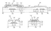
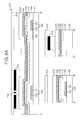
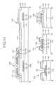
- FIG. 1is a plan view illustrating a thin film transistor substrate using a four-mask process
- FIG. 2is a section view of the thin film transistor substrate taken along the I-I′ line in FIG. 1 .
- the thin film transistor substrateincludes a gate line 2 and a data line 4 provided on a lower substrate 42 in such a manner to cross each other while with having a gate insulating film 44 therebetween, a thin film transistor 6 provided at each crossing, and a pixel electrode 18 provided at a cell area having the crossing structure.
- the thin film transistor substrateincludes a storage capacitor 20 provided at an overlapped portion between the pixel electrode 18 and a previous gate line 2 , a gate pad 26 connected to the gate line 2 , and a data pad 34 connected to the data line 4 .
- the thin film transistor 6allows a pixel signal applied to the data line 4 to be charged into the pixel electrode 18 and kept in response to a scanning signal applied to the gate line 2 .
- the thin film transistor 6includes a gate electrode 8 connected to the gate line 2 , a source electrode 10 connected to the data line 4 , a drain electrode 12 connected to the pixel electrode 18 , and an active layer 14 overlapping with the gate electrode 8 and defining a channel between the source electrode 10 and the drain electrode 12 .
- the active layer 14 overlapping with the source electrode 10 and the drain electrode 12 and having a channel portion between the source electrode 10 and the drain electrode 12also overlaps with the data line 4 , a lower data pad electrode 36 and a storage electrode 22 .
- an ohmic contact layer 48 for making an ohmic contact with the data line 4 , the source electrode 10 , the drain electrode 12 , the lower data pad electrode 36 and the storage electrode 22are further provided.
- the pixel electrode 18is connected, via a first contact hole 16 passing through a passivation film 50 , to the drain electrode 12 of the thin film transistor 6 .
- the pixel electrode 18generates a potential difference with respect to a common electrode provided at an upper substrate (not shown) by the charged pixel signal. This potential difference rotates a liquid crystal positioned between the thin film transistor substrate and the upper substrate owing to a dielectric anisotropy and transmits a light input, via the pixel electrode 18 , from a light source (not shown) toward the upper substrate.
- the storage capacitor 20includes a previous gate line 2 , a upper storage electrode 22 overlapping the gate line 2 and having the gate insulating film 44 , the active layer 14 and the ohmic contact layer 48 therebetween, and a pixel electrode 18 overlapping the upper storage electrode 22 and having the passivation film 50 therebetween and connected via a second contact hole 24 passing through the passivation film 50 .
- the storage capacitor 20allows a pixel signal charged in the pixel electrode 18 to be stably maintained until a next pixel voltage is charged.
- the gate line 2is connected, via the gate pad 26 , to a gate driver (not shown).
- the gate pad 26consists of a lower gate pad electrode 28 extended from the gate line 2 , and an upper gate pad electrode 32 connected, via a third contact hole 30 passing through the gate insulating film 44 and the passivation film 50 , to the lower gate pad electrode 28 .
- the data line 4is connected, via the data pad 34 , to the data driver (not shown).
- the data pad 34includes a lower data pad electrode 36 extended from the data line 4 , and an upper data pad electrode 40 connected, via a fourth contact hole 38 passing through the passivation film 50 , to the lower data pad electrode 36 .
- a gate pattern including the gate line 2 , the gate electrode 8 and the lower gate pad electrode 28is provided on the lower substrate 42 by the first mask process.
- a gate metal layeris formed on the lower substrate 42 by a deposition technique such as sputtering. Then, the gate metal layer is patterned by a photolithography and etching process using a first mask to thereby form a gate pattern including the gate line 2 , the gate electrode 8 and the lower gate pad electrode 28 .
- the gate metal layermay have a single-layer or double-layer structure of chrome (Cr), molybdenum (Mo) or an aluminum group metal, etc.
- the gate insulating film 44is formed on the lower substrate 42 provided with the gate pattern. Further, a semiconductor pattern including the active layer 14 and the ohmic contact layer 48 and source/drain pattern including the data line 4 , the source electrode 10 , the drain electrode 12 , the lower data pad electrode 36 and the storage electrode 22 are sequentially provided on the gate insulating film 44 by the second mask process.
- the gate insulating film 44an amorphous silicon layer, a n + amorphous silicon layer and a source/drain metal layer are sequentially provided on the lower substrate 42 provided with the gate pattern by deposition techniques such as plasma enhanced chemical vapor deposition (PECVD) and sputtering, etc.
- PECVDplasma enhanced chemical vapor deposition
- the gate insulating film 44is formed from an inorganic insulating material such as silicon nitride (SiN x ) or silicon oxide (SiO x ).
- the source/drain metalmay be selected from molybdenum (Mo) or a molybdenum alloy, etc.
- a photo-resist patternis formed on the source/drain metal layer by the photolithography using a second mask.
- a diffractive exposure mask having a diffractive exposing part at a channel portion of the thin film transistoris used as a second mask, thereby allowing a photo-resist pattern of the channel portion to have a lower height than other source/drain pattern portion.
- the source/drain metal layeris patterned by a wet etching process using the photo-resist pattern to thereby provide the source/drain pattern including the data line 4 , the source electrode 10 , the drain electrode 12 being integral to the source electrode 10 and the storage electrode 22 .
- the n + amorphous silicon layer and the amorphous silicon layerare patterned at the same time by a dry etching process using the same photo-resist pattern to thereby provide the ohmic contact layer 48 and the active layer 14 .
- the photo-resist pattern having a relatively low heightis removed from the channel portion by a ashing process and thereafter the source/drain pattern and the ohmic contact layer 48 of the channel portion are etched by the dry etching process.
- the active layer 14 of the channel portionis exposed to disconnect the source electrode 10 from the drain electrode 12 .
- the photo-resist pattern left on the source/drain metal pattern groupis removed by a stripping process.
- the passivation film 50 including the first to fourth contact holes 16 , 24 , 30 and 38are formed on the gate insulating film 44 provided with the source/drain pattern.
- the passivation film 50is formed entirely on the gate insulating film 44 provided with the source/drain pattern by a deposition technique such as the plasma enhanced chemical vapor deposition (PECVD). Then, the passivation film 50 is patterned by the photolithography and etching process using a third mask to thereby define the first to fourth contact holes 16 , 24 , 30 and 38 .
- the first contact hole 16is formed in such a manner to pass through the passivation film 50 and expose the drain electrode 12
- the second contact hole 24is formed in such a manner as to pass through the passivation film 50 and expose the upper storage electrode 22 .
- the third contact hole 30is formed in such a manner as to pass through the passivation film 50 and the gate insulating film 44 and expose the lower gate pad electrode 28 .
- the fourth contact hole 38is formed in such a manner as to pass through the passivation film 50 and expose the upper data pad electrode 36 .
- the passivation film 50is formed of an inorganic insulating material identical to the gate insulating film 44 , or an organic insulating material such as an acrylic organic compound having a small dielectric constant, BCB (benzocyclobutene) or PFCB (perfluorocyclobutane), etc.
- a transparent conductive pattern including the pixel electrode 18 , the upper gate pad electrode 32 and the upper data pad electrode 40is provided on the passivation film 50 by the fourth mask process.
- a transparent conductive layeris formed on the passivation film 50 by a deposition technique such as sputtering, etc. Then, the transparent conductive layer is patterned by photolithography and an etching process using a fourth mask to thereby provide the transparent conductive pattern including the pixel electrode 18 , the upper gate pad electrode 32 and the upper data pad electrode 40 .
- the pixel electrode 18is electrically connected, via the first contact hole 16 , to the drain electrode 12 while being electrically connected, via the second contact hole 24 , to the upper storage electrode 22 overlapping with a previous gate line 2 .
- the upper gate pad electrode 32is electrically connected, via the third contact hole 30 , to the lower gate pad electrode 28 .
- the upper data pad electrode 40is electrically connected, via the fourth contact hole 38 , to the lower data pad electrode 36 .
- the transparent conductive layeris formed of indium-tin-oxide (ITO), etc.
- the related art thin film transistor substrate and the fabricating methoduses a four-mask process, thereby reducing the number of processes and hence reducing manufacturing costs in proportion to the reduction in the number of processes.
- the upper and lower electrodes of the storage capacitor 20are formed of an opaque source/drain metal and an opaque gate metal, respectively.
- the problemarises in that, when an overlapping area between the upper storage electrode 22 and the gate line 2 is enlarged so as to increase a capacitance of the storage capacitor 20 , an aperture ratio of the pixel electrode 18 is reduced.
- the present inventionis directed to liquid crystal display device and fabricating method thereof that substantially obviates one or more of the problems due to limitations and disadvantages of the related art.
- An advantage of the present inventionto provide a thin film transistor substrate and a fabricating method thereof that are adaptive for simplifying a process as well as enlarging a capacitance value of a storage capacitor without any reduction of aperture ratio.
- a liquid crystal display deviceincludes: a double-layered gate line having a first transparent conductive layer and a second opaque conductive layer, the second opaque conductive layer having a step coverage; a gate insulation film on the gate line; a data line crossing the gate line to define a pixel region; a thin film transistor connected to the gate line and the data line; a pixel electrode connected to the thin film transistor via a contact hole of a protective film on the thin film transistor; and a storage capacitor overlapping the pixel electrode and having a lower storage electrode formed of the first transparent conductive layer.
- a method of fabricating a liquid crystal display deviceincludes: forming a gate pattern including a gate line, a gate electrode and a lower storage electrode on a substrate using a first mask, the gate line and the gate electrode being formed of a double-layer having a transparent conductive layer, and the lower storage electrode being formed of the transparent conductive layer; forming a gate insulating film on the gate pattern; forming a semiconductor pattern and a source/drain pattern having a data line and source and drain electrodes on the gate insulating film using a second mask, the data line defining a pixel region with the gate line; forming a protective film on the source and drain electrodes, and forming a contact hole exposing the drain electrode using a third mask; and forming a pixel electrode connected to the drain electrode via the contact hole on the protective film and overlapping with the lower storage electrode using a fourth mask.
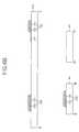
- FIG. 1is a plan view showing a portion of a related art thin film transistor substrate
- FIG. 2is a section view of the thin film transistor substrate taken along the I-I′ line in FIG. 1 ;
- FIG. 3A to FIG. 3Dare section views illustrating a method of fabricating the thin film transistor substrate shown in FIG. 2 ;
- FIG. 4is a plan view showing a portion of a thin film transistor substrate according to an embodiment of the present invention.
- FIG. 5is a section view of the thin film transistor substrate taken along the II′, III-III′ and IV-IV′ lines in FIG. 4 ;
- FIG. 6A and FIG. 6Bare a plan view and a section view for explaining a first mask process of the thin film transistor substrate according to the embodiment of the present invention.
- FIG. 7A to FIG. 7Eare section views for specifically explaining the first mask process
- FIG. 8A and FIG. 8Bare a plan view and a section view for explaining a second mask process of the thin film transistor substrate according to the embodiment of the present invention.
- FIG. 9A to FIG. 9Eare section views for specifically explaining the second mask process
- FIG. 10A to FIG. 10Care a plan view and section views for explaining a third mask process of the thin film transistor substrate according to the embodiment of the present invention.
- FIG. 11A and FIG. 11Bare a plan view and a section view for explaining a fourth mask process of the thin film transistor substrate according to the embodiment of the present invention.
- FIG. 12is a section view showing a gate pattern in a thin film transistor substrate according to a second embodiment of the present invention.
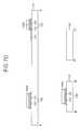
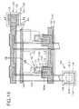
- FIG. 13is a plan view showing a portion of a thin film transistor substrate according to a third embodiment of the present invention.
- FIG. 14is a section view of the thin film transistor substrate taken along the II-II′, III-III′, IV-IV′ and V-V′ lines in FIG. 13 ;
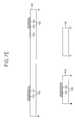
- FIG. 15is a plan view showing a portion of a thin film transistor substrate according to a fourth embodiment of the present invention.
- FIG. 16is a section view of the thin film transistor substrate taken along the III-III′, IV-IV′ and VI-VI′ lines in FIG. 15 ;
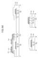
- FIG. 17is a plan view showing a portion of a thin film transistor substrate according to a fifth embodiment of the present invention.
- FIG. 18is a section view of the thin film transistor substrate taken along the III-III′, IV-IV′ and VII-VII′ lines in FIG. 17 ;
- FIG. 19is a plan view showing a portion of a thin film transistor substrate according to a sixth embodiment of the present invention.
- FIG. 20is a section view of the thin film transistor substrate taken along the III-III′, IV-IV′ and VIII-VIII′ lines in FIG. 19 .
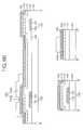
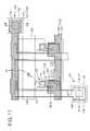
- FIG. 4is a plan view showing a portion of a thin film transistor substrate according to an embodiment of the present invention
- FIG. 5is a section view of the thin film transistor substrate taken along the II-II′, III-III′ and IV-IV′ lines in FIG. 4 .
- the thin film transistor substrateincludes a gate line 102 and a data line 104 provided on a lower substrate 142 in such a manner as to cross each other, the data line 104 and gate line 102 having a gate insulating film 144 therebetween, a thin film transistor 106 being adjacent to each crossing, and a pixel electrode 118 provided at a pixel area defined by the crossing structure.
- the thin film transistor substrateincludes a storage capacitor 120 provided at an overlapped portion between the pixel electrode 118 and a lower storage electrode 122 connected to a previous gate line 102 , a gate pad 126 connected to the gate line 102 , and a data pad 134 connected to the data line 104 .
- the thin film transistor 106allows a pixel signal applied to the data line 104 to be charged into the pixel electrode 118 and be kept in response to a scanning signal applied to the gate line 102 .
- the thin film transistor 106includes a gate electrode 108 connected to the gate line 102 , a source electrode 110 connected to the data line 104 , a drain electrode 112 positioned opposite the source electrode 110 and connected to the pixel electrode 118 , an active layer 114 overlapping with the gate electrode 108 with having the gate insulating film 144 therebetween to define a channel between the source electrode 110 and the drain electrode 112 , and an ohmic contact layer 146 formed on the active layer 114 other than the channel portion to make an ohmic contact with the source electrode 110 and the drain electrode 112 .
- the gate line 102 and the gate electrode 108have a double-layered structure in which a first conductive layer 101 formed from a transparent conductive layer and a second conductive layer 103 formed from a metal layer thereon are disposed.
- the semiconductor pattern 148 including the active layer 114 and the ohmic contact layer 146also overlap with the data line 104 .
- a pixel area defined by a crossing between the gate line 102 and the data line 104is provided with a pixel electrode 118 .
- the pixel electrode 118is connected, via a first contact hole 116 passing through the passivation film 150 , to the drain electrode 112 .
- Such a pixel electrode 118charges a pixel signal supplied from the thin film transistor 106 to thereby generate a potential difference with respect to a common electrode provided at a color filter substrate (not shown).
- This potential differencerotates a liquid crystal positioned between the thin film transistor substrate and the color filter substrate based on a dielectric anisotropy and controls an amount of a light input, via the pixel electrode 118 , from a light source (not shown) to thereby transmit it into the color filter substrate.
- the storage capacitor 120is formed such that the lower storage electrode 122 protruded from the first conductive layer 101 toward the pixel area overlaps with the pixel electrode 118 with the gate insulating film 144 and the passivation film 150 therebetween.
- the lower storage electrode 122is formed from the first conductive layer 101 , that is, a transparent conductive layer, so that an overlapping area between it and the pixel area can be enlarged without a reduction of aperture ratio. Accordingly, it becomes possible to increase a capacitance of the storage capacitor 120 without any reduction of aperture ratio, and hence to keep the signal charged in the pixel electrode 118 more stable.
- the gate line 102is connected, via the gate pad 126 , to a gate driver (not shown).
- the gate pad 126includes a lower gate pad electrode 128 extended from the gate line 102 , and an upper gate pad electrode 132 connected, via a second contact hole 130 passing through the passivation film 150 and the gate insulating film 144 , to the lower gate pad electrode 128 .
- the lower gate pad electrode 128has a double-layered structure in which the first and second conductive layers 101 and 103 are formed like the gate line 102 .
- the data line 104is connected, via a data pad 134 , to a data driver (not shown).
- the data pad 134consists of a lower data pad electrode 136 extended from the data line 104 , and an upper data pad electrode 140 connected, via a third contact hole 138 passing through the passivation film 150 , to the lower data pad electrode 136 .
- the semiconductor layer 148 including the ohmic contact layer 146 and the active layer 114is formed under the lower data pad electrode 136 in such a manner to overlap with it.
- the thin film transistor substrate according to the embodiment of the present inventionforms the lower storage electrode 122 , overlapped by the pixel electrode 118 , from a transparent conductive layer, so that a capacitance of the storage capacitor 120 can be increased without any reduction of aperture ratio. Accordingly, a line width of the gate line 102 can be reduced independently of an overlapping area between the gate line 102 and the pixel electrode 118 , thereby having an advantage in making a high definition.
- the thin film transistor substrate according to the embodiment of the present invention having the above-mentioned structureis formed by the following four-mask process.
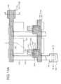
- FIG. 6A and FIG. 6Bare a plan view and a section view, respectively, for explaining a first mask process in a method of fabricating the thin film transistor substrate according to the embodiment of the present invention
- FIG. 7A to FIG. 7Eare section views specifically explaining the first mask process.
- a gate pattern including the gate line 102 , the gate electrode 108 connected to the gate line 102 , the lower gate pad electrode 128 and the lower storage electrode 122is formed on the lower substrate 142 by a first mask process.
- the gate line 102 , the gate electrode 108 and the lower gate pad electrode 128have a double-layered structure in which the first and second conductive layers 101 and 103 are formed, whereas the lower storage electrode 122 has a single-layered structure in which the first conductive layer 101 of the gate line 102 is extended.
- the gate pattern having the above-mentioned double-layered and single-layered structureis formed by a single mask process using a half tone mask 160 .
- the first and second conductive layers 101 and 103are formed on the lower substrate 142 by a deposition technique such as sputtering, and a photo-resist 176 is formed thereon.
- the first conductive layer 101is formed of a transparent conductive material such as indium-tin-oxide (ITO), tin-oxide (TO), indium-zinc-oxide (IZO) or the like.
- the second conductive layer 103is formed of a metal material such as Mo, Cu, Al, Ti, Cr, MoW or AlNd, etc.
- the photo-resist 167is exposed to light and developed by photolithography using a half tone mask 160 , thereby forming a photo-resist pattern 168 having a step coverage as shown in FIG. 7B .
- the half tone mask 160includes a transparent quartz (SiO 2 ) substrate 166 , and a shielding layer 162 and a partial transmitting layer 164 formed thereon.
- the shielding layer 162is positioned at an area to be provided with a gate pattern to shut off an ultraviolet ray (UV), thereby leaving a first photo-resist pattern 168 A after a development thereof.
- the partial transmitting layer 164is positioned at an area to be provided with the lower storage electrode to partially transmit the UV, thereby leaving a second photo-resist pattern 168 B thinner than the first photo-resist pattern 168 A.
- the shielding layer 162is formed of a metal such as Cr, CrO x or the like, whereas the partial transmitting layer 164 is made from MoSi x .
- a diffractive exposure maskalso is applicable.
- the first and second conductive layers 101 and 103are patterned by an etching process using the photo-resist pattern 168 having a step coverage to thereby provide a double-layer structure of gate pattern as shown in FIG. 7C .
- the photo-resist pattern 168is ashed by an ashing process using an oxygen (O 2 ) plasma to thereby thin the thickness of the first photo-resist pattern 168 A and remove the second photo-resist pattern 168 B as shown in FIG. 7D .
- the second conductive layer 103 on the lower storage electrode 122is removed by an etching process using the ashed first photo-resist pattern 168 A.
- the lower storage electrode 122can be formed from only the first conductive layer 101 without a miss-alignment to the second conductive layer 103 included in the gate line 102 .
- each side of the second conductive layer 103 patterned along the ashed first photo-resist pattern 168 Ais once more etched, thereby allowing the first and second conductive layers 101 and 103 of the gate pattern to have a certain step coverage in a stepwise shape. Accordingly, when the side surfaces of the first and second conductive layers 101 and 103 have a high steep slope, it becomes possible to prevent a breakage badness of the source/drain metal layer that may be generated thereon.
- the etching process of the first and second conductive layers 101 and 103may selectively employ wet etching or dry etching. For instance, if all the first and second conductive layers 101 and 103 are etched, then the etching process of the first and second layers 101 and 103 as shown in FIG. 7C ; and the ashing process of the photo-resist pattern and the etching process of the exposed second conductive layer 103 as shown in FIG. 7D are successively performed at the same chamber, so that an advantage of a process simplification can be obtained.
- the etching process of the exposed second conductive layer 103may employ wet etching.
- the first and second conductive layers 101 and 103may employ wet etching as shown in FIG. 7C
- both the ashing process and the etching process of the exposed second conductive layer 103may employ a dry etching or the etching process of the exposed second conductive layer 103 only may employ a wet etching as shown in FIG. 7D .
- the second conductive layer 103performs a wet etching while the first conductive layer 101 performs a dry etching, or the second conductive layer 103 performs a dry etching and the first conductive layer 101 performs a wet etching; and thereafter both the ashing process and the etching process of the exposed second conductive layer 103 employ a dry etching or only the etching process of the exposed second conductive layer 103 employs a wet etching.
- dry etchingis advantageous when it is applied to a high-definition model, whereas wet etching is advantageous when it is applied to a high-dimension model. Further, dry etching is advantageous when the second conductive layer 103 is formed of Mo, whereas a wet etching is advantageous when the second conductive layer 103 is made from Cu or Al.
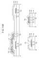
- FIG. 8A and FIG. 8Bare a plan view and a section view for explaining a second mask process, respectively, in a method of fabricating the thin film transistor substrate according to an embodiment of the present invention
- FIG. 9A to FIG. 9Eare section views explaining the second mask process in detail.
- the gate insulating film 144is formed on the lower substrate 142 provided with the gate pattern. Further, the source/drain pattern including the data line 104 , the source electrode 110 , the drain electrode 112 and the lower data pad electrode 136 and the semiconductor pattern 148 including the active layer 114 and the ohmic contact layer 146 overlapping each other along the rear side of the source/drain pattern are formed thereon by the second mask process.
- the semiconductor pattern 148 and the source/drain patternare formed by a single mask process using a diffractive exposure mask.
- the gate insulating film 144 , an amorphous silicon layer 115 , an amorphous silicon layer 145 being doped with n + or p + impurity and the source/drain metal layer 105are sequentially formed on the lower substrate 142 provided with the gate pattern.
- the gate insulating film 144 , the amorphous silicon layer 115 and the amorphous silicon doped with the impuritymay be formed by PECVD, whereas the source/drain metal layer 105 is formed by sputtering.
- the gate insulating film 144is formed of an inorganic insulating material such as silicon nitride (SiN x ) or silicon oxide (SiO x ), whereas the source/drain metal layer 105 is formed of Cr, MoW, Al/Cr, Cu, Al(Nd), Al/Mo, Al(Nd)/Al, Al(Nd)/Cr, Mo/Al(Nd)/Mo, Cu/Mo or Ti/Al(Nd)/Ti, etc.
- a double layer of Al/Crmeans that Cr should be formed first and Al should be formed later.
- a photo-resist 219is formed on the source/drain metal layer 105 and then is exposed to the light and developed by photolithography using a diffractive exposure mask 210 , thereby providing a photo-resist pattern 220 having a step coverage as shown in FIG. 9B .
- the diffractive exposure mask 210includes a transparent quartz substrate 212 , a shielding layer 214 formed from a metal layer such as Cr, CrO x or the like, and a diffractive exposure slit 216 .
- the shielding layer 214is positioned at an area to be provided with the semiconductor pattern and the source/drain pattern to shut off an ultraviolet ray (UV), thereby leaving a first photo-resist pattern 220 A after a development thereof.
- the diffractive exposure slit 216is positioned at an area to be provided with a channel of the thin film transistor to diffract the UV, thereby leaving a second photo-resist pattern 220 B thinner than the first photo-resist pattern 220 A.
- the source/drain metal layer 105is patterned by an etching process using the photo-resist pattern 220 having a step coverage to thereby provide the source/drain pattern and the semiconductor pattern 148 under it as shown in FIG. 9C .
- the source electrode 110 and the drain electrode 112 of this source/drain patternhave an integral structure.
- the photo-resist pattern 220is ashed by the ashing process using an oxygen (O 2 ) plasma to thereby thin the thickness of the first photo-resist pattern 220 A and remove the second photo-resist pattern 220 B as shown in FIG. 9D .
- the source/drain pattern exposed by a removal of the second photo-resist pattern 220 B and the ohmic contact layer under itis removed by an etching process using the ashed first photo-resist pattern 220 A, thereby disconnecting the source electrode 110 from the drain electrode 112 and exposing the active layer 114 .
- a channel consisting of the active layer 114is provided between the source electrode 110 and the drain electrode 112 .
- each side of the source/drain patternis once more etched along the ashed first photo-resist pattern 220 A to provide the source/drain pattern and semiconductor pattern 148 having a step coverage in a stepwise shape.
- the photo-resist pattern 220 A left on the source/drain patternis removed by a stripping process as shown in FIG. 9E .
- FIG. 10A to FIG. 10Care a plan view and section views for explaining a third mask process in a method of fabricating the thin film transistor substrate according to the embodiment of the present invention.
- the passivation film 150 having a plurality of contact holes 116 , 130 and 138is formed by the gate insulating film 144 provided with the source/drain pattern by the third mask process.
- the passivation film 150is formed on the gate insulating film 144 provided with the source/drain pattern by a technique such as the PECVD and spin coating, etc.
- the passivation film 150is formed of an inorganic insulating material identical to the gate insulating film 144 , or an organic insulating material such as an acrylic organic compound having a small dielectric constant, BCB (benzocyclobutene) or PFCB (perfluorocyclobutane), etc.
- BCBbenzocyclobutene
- PFCBperfluorocyclobutane
- the first and third contact holes 116 and 138are formed in such a manner to pass through the active layer 114 as shown in FIG. 10C .
- FIG. 11A and FIG. 11Bare a plan view and a section view explaining a fourth mask process in a method of fabricating the thin film transistor substrate according to the embodiment of the present invention
- a transparent conductive pattern including the pixel electrode 118 , the upper gate pad electrode 132 and the upper data pad electrode 140is formed on the passivation film 150 by the fourth mask process.
- the transparent conductive patternis formed by preparing a transparent conductive layer using a deposition technique such as the sputtering, etc. and patterning it by the photolithography and the etching process.
- the transparent conductive layeris formed of ITO, TO or IZO, etc. similar to the first conductive layer 101 of the above-mentioned gate pattern.
- the pixel electrode 118is connected, via the first contact hole 116 , to the drain electrode 112 ; the upper gate pad electrode 132 is connected, via the second contact hole 130 , to the lower gate pad electrode 128 ; and the upper data pad electrode 140 is connected, via the third contact hole 138 , to the lower data pad electrode 136 .
- the method of fabricating the thin film transistor substrate according to the embodiment of the present inventionforms the gate pattern having a double-layer structure and the lower storage electrode 122 having a single-layer structure using the half-tone mask, thereby simplifying a process by the four-mask process. Furthermore, the method of fabricating the thin film transistor substrate according to the embodiment of the present invention uses the half tone mask when it is intended to thinly form the photo-resist pattern corresponding to a relatively wide area like the lower storage electrode 122 while using the diffractive exposure mask when it is intended to thinly form the photo-resist pattern corresponding to a relatively narrow area like the channel of the thin film transistor 106 , thereby improving a process efficiency.
- FIG. 12is a section view showing only a gate pattern formed by a first mask process in a thin film transistor substrate according to a second embodiment of the present invention.
- the gate pattern shown in FIG. 12includes a gate line 202 , a gate electrode 208 and a lower gate pad electrode 228 having a triple-layer structure in which the first to third conductive layers 201 , 203 and 205 are disposed, and a lower storage electrode 222 provided such that the first conductive layer 201 of the gate line 202 is extended into a pixel area.
- the gate pattern having the above-mentioned triple-layer and single-layer structureis formed by a single mask process using a half tone mask.
- the gate pattern having the triple-layer structurehas a reduced line resistance such that it is may be used for a large-dimension or high-definition panel.
- the first conductive layer 201is formed of a transparent conductive material such as indium-tin-oxide (ITO), tin-oxide (TO), indium-zinc-oxide (IZO) or the like.
- the second conductive layer 203is formed of a metal material such as Mo, Ti, Cu or Al(Nd) group, etc.
- the third conductive layer 205is formed from a metal material such as Cu, Al, Ti, Mo or Al(Nd) group, etc., and the second and third conductive layers 203 and 205 may be formed of a combination of these groups.
- theymay be formed of Mo/ITO, Al(Nd)/ITO, Cu/ITO, Cu/Ti/ITO, Cu/Mo/ITO, Cu/Mo/ITO, Cu/Mo+Ti/ITO or Al(Nd)/Mo/ITO, etc.
- a more than double layer of Mo/ITOmeans that ITO should be formed first and Mo should be formed later.
- FIG. 13is a plan view showing a portion of a thin film transistor substrate according to a third embodiment of the present invention
- FIG. 14is a section view of the thin film transistor substrate taken along the II-II′, III-II′, IV-IV′ and V-V′ lines in FIG. 13 .
- the thin film transistor substrate shown in FIG. 13 and FIG. 14has the same elements as the thin film transistor substrate shown in FIG. 4 and FIG. 5 except that it further includes a redundancy line overlapping with the data line 104 . Therefore, an explanation as to the same elements will be omitted.
- the redundancy line 170is connected to the data line 104 by a welding technique using a laser or the like upon a breakage or defection of the data line 104 to thereby repair the broken data line 104 .
- the redundancy line 170may be formed as a single-layer structure like the lower storage electrode 122 or a double-layer (or triple-layer) structure like the gate line 102 , along with the gate pattern including the gate line 102 , the gate electrode 108 , the lower gate pad electrode 128 and the lower storage electrode 122 , by the half tone mask process. Further, the redundancy line 170 is formed independently between the gate lines 102 and floated such that it is not shorted with respect to the gate line 102 provided at the same layer.
- FIG. 15is a plan view showing a portion of a thin film transistor substrate according to a fourth embodiment of the present invention
- FIG. 16is a section view of the thin film transistor substrate taken along the III-III′, IV-IV′ and VI-VI′ lines in FIG. 15 .
- the thin film transistor substrate shown in FIG. 15 and FIG. 16has the same elements as the thin film transistor substrate shown in FIG. 4 and FIG. 5 except that it further includes a light-shielding pattern 172 overlapping with each side of the pixel electrode 118 . Therefore, an explanation as to the same elements will be omitted.
- the light-shielding pattern 172is formed such that the second conductive layer 103 is extended from the gate line 102 to thereby overlap with each side of the pixel electrode 118 , whereas the lower storage electrode 122 is formed in such a manner as to overlap with the light-shielding pattern 172 for the sake of a process.
- the light-shielding pattern 172prevents a light leakage between the data line 104 and the pixel electrode 118 when it is intended to enlarge a distance between the data line 104 and the pixel electrode 118 for the purpose of reducing a parasitic capacitor.
- the light-shielding pattern 172is formed from the second conductive layer 102 , along with the gate pattern including the gate line 102 , the gate electrode 108 , the lower gate pad electrode 128 and the lower storage electrode 122 , by the half tone mask process.
- the lower portion of the light-shielding pattern 172overlaps with the lower storage electrode 122 that is the first conductive layer 101 .
- FIG. 17is a plan view showing a portion of a thin film transistor substrate according to a fifth embodiment of the present invention
- FIG. 18is a section view of the thin film transistor substrate taken along the III-III′, IV-IV′ and VII-VII′ lines in FIG. 17 .
- the thin film transistor substrate shown in FIG. 17 and FIG. 18has the same elements as the thin film transistor substrate shown in FIG. 4 and FIG. 5 except that a storage capacitor 180 is formed by an overlap between the common line 182 and the pixel electrode 118 . Therefore, an explanation as to the same elements will be omitted.
- the storage capacitor 180is formed such that the common line 182 is overlapped by the pixel electrode 118 having the gate insulating film 144 and the passivation film 150 therebetween.
- the common line 182crosses the pixel electrode 118 and the data line 104 substantially parallel to the gate line 102 .
- the common line 182is formed, along with the gate pattern including the gate line 102 , the gate electrode 198 and the lower gate pad electrode 128 , by the halftone mask process.
- the common line 182is formed from only the first conductive layer 101 that is a transparent conductive layer unlike a double-layer (or triple-layer) structure of gate pattern by utilizing a partial transmitting part of the half tone mask.
- both the pixel electrode 118 and the common line 182 that are the upper and lower electrodes of the storage capacitor 180 , respectively,are formed from a transparent conductive layer, so that it becomes possible to enlarge an overlap area between two electrodes 118 and 182 without any reduction of aperture ratio and hence to increase a capacitance value of the storage capacitor 180 .
- FIG. 19is a plan view showing a portion of a thin film transistor substrate according to a sixth embodiment of the present invention
- FIG. 20is a section view of the thin film transistor substrate taken along the III-III′, IV-IV′ and VIII-VII′ lines in FIG. 19 .
- the thin film transistor substrate shown in FIG. 19 and FIG. 20has the same elements as the thin film transistor substrate shown in FIG. 4 and FIG. 5 except that a storage capacitor 190 is formed by an overlap among the common line 182 , the lower storage electrode 194 connected thereto and the pixel electrode 118 . Therefore, an explanation as to the same elements will be omitted.
- the storage capacitor 190is formed such that the common line 192 and the lower storage electrode 194 are overlapped by the pixel electrode 118 with the gate insulating film 144 and the passivation film 150 therebetween.
- the common line 192is formed by a double-layer (or triple-layer) structure crossing the pixel electrode 118 and the data line 104 substantially parallel to the gate line 102 .
- the lower storage electrode 194is formed by a protrusion of the first conductive layer 101 , that is, the transparent conductive layer, of the common line 192 at each pixel area.
- the common line 182 and the lower storage electrode 194are formed, along with the gate pattern including the gate line 102 , the gate electrode 198 and the lower gate pad electrode 128 , by the half tone mask process.
- the lower storage electrode 194is formed from only the first conductive layer 101 that is a transparent conductive layer unlike a double-layer (or triple-layer) structure of gate pattern and the common line 192 by utilizing a partial transmitting part of the half tone mask. Accordingly, an overlap area between the lower storage electrode 194 and the pixel electrode 118 can be enlarged without any reduction of aperture ratio to increase a capacitance value of the storage capacitor 190 .
- the common line 192takes a double-layer (or triple-layer) structure like the gate pattern to reduce a line resistance, so that a line width of the common line 192 can be reduced to minimize a parasitic capacitor caused by an intersection between the common line 192 and the data line 104 .
- both the upper and lower electrodes of the storage capacitorare formed from a transparent conductive layer, so that it becomes possible to enlarge an overlap area between two electrodes without any reduction of aperture ratio and hence to increase a capacitance value of the storage capacitor.
- a single-layer structure of a lower storage electrodeis formed, along with a double-layer (or triple-layer) structure of gate pattern, by utilizing the half tone mask, thereby simplifying a process.
- the first and second conductive layers of the gate pattern taking a double-layer (or triple-layer) structurehas a constant step coverage in a stepwise shape by the half-tone mask process, so that it becomes possible to prevent a breakage of the source/drain pattern caused by an inclination of the first and second conductive layers.
Landscapes
- Physics & Mathematics (AREA)
- Nonlinear Science (AREA)
- Engineering & Computer Science (AREA)
- Microelectronics & Electronic Packaging (AREA)
- Mathematical Physics (AREA)
- Chemical & Material Sciences (AREA)
- Crystallography & Structural Chemistry (AREA)
- General Physics & Mathematics (AREA)
- Optics & Photonics (AREA)
- Liquid Crystal (AREA)
- Thin Film Transistor (AREA)
- Devices For Indicating Variable Information By Combining Individual Elements (AREA)
Abstract
Description
- This application claims the benefit of Korean Patent Application No. P2004-37770 filed in Korea on May 27, 2004, which is hereby incorporated by reference for all purposes as if fully set forth herein.
- 1. Field of the Invention
- This invention relates to a thin film transistor substrate applied to a display device, and more particularly to a thin film transistor substrate and a fabricating method thereof that are adaptive for simplifying a process.
- 2. Discussion of the Related Art
- Generally, a liquid crystal display (LCD) controls light transmittance of a liquid crystal using an electric field to thereby display a picture. To this end, the LCD includes a liquid crystal display panel having liquid crystal cells arranged in a matrix, and a driving circuit for driving the liquid crystal display panel.
- The liquid crystal display panel includes a thin film transistor substrate and a color filter substrate opposed to each other, a liquid crystal injected between two substrates, and a spacer maintaining cell gap between the two substrates.
- The thin film transistor substrate includes gate lines, data lines, thin film transistors formed as switching devices for each crossing between the gate lines and the data lines, pixel electrodes formed for each liquid crystal cell and connected to the thin film transistor, and alignment films formed thereon. The gate lines and the data lines receive signals from the driving circuits via each pad portion. The thin film transistor applies a pixel signal fed to the data line to the pixel electrode in response to a scanning signal fed to the gate line.
- The color filter substrate includes color filters formed for each liquid crystal cell, black matrices for dividing color filters and reflecting an external light, common electrodes for commonly applying reference voltages to the liquid crystal cells, and an alignment film formed thereon.
- The liquid crystal display panel is completed by preparing the thin film array substrate and the color filter substrate individually to join them and then injecting a liquid crystal between them and sealing it.
- In such a liquid crystal display device, the thin film transistor substrate has a complicated fabrication process that leads to a major rise in a manufacturing cost of the liquid crystal display panel because it involves a semiconductor process and needs a plurality of mask processes. In order to solve this, the thin film transistor substrate has been developed toward a reduction in the number of mask processes. This is because one mask process includes processes such as thin film deposition, cleaning, photolithography, etching, photo-resist stripping and inspection processes, etc. Recently, there has been highlighted a four-mask process excluding one mask process from the existent five-round mask process that was a standard mask process of the thin film transistor.
FIG. 1 is a plan view illustrating a thin film transistor substrate using a four-mask process, andFIG. 2 is a section view of the thin film transistor substrate taken along the I-I′ line inFIG. 1 .- In
FIG. 1 andFIG. 2 , the thin film transistor substrate includes agate line 2 and adata line 4 provided on alower substrate 42 in such a manner to cross each other while with having agate insulating film 44 therebetween, athin film transistor 6 provided at each crossing, and apixel electrode 18 provided at a cell area having the crossing structure. Further, the thin film transistor substrate includes astorage capacitor 20 provided at an overlapped portion between thepixel electrode 18 and aprevious gate line 2, agate pad 26 connected to thegate line 2, and adata pad 34 connected to thedata line 4. - The
thin film transistor 6 allows a pixel signal applied to thedata line 4 to be charged into thepixel electrode 18 and kept in response to a scanning signal applied to thegate line 2. To this end, thethin film transistor 6 includes agate electrode 8 connected to thegate line 2, asource electrode 10 connected to thedata line 4, adrain electrode 12 connected to thepixel electrode 18, and anactive layer 14 overlapping with thegate electrode 8 and defining a channel between thesource electrode 10 and thedrain electrode 12. - The
active layer 14 overlapping with thesource electrode 10 and thedrain electrode 12 and having a channel portion between thesource electrode 10 and thedrain electrode 12 also overlaps with thedata line 4, a lowerdata pad electrode 36 and astorage electrode 22. On theactive layer 14, anohmic contact layer 48 for making an ohmic contact with thedata line 4, thesource electrode 10, thedrain electrode 12, the lowerdata pad electrode 36 and thestorage electrode 22 are further provided. - The
pixel electrode 18 is connected, via afirst contact hole 16 passing through apassivation film 50, to thedrain electrode 12 of thethin film transistor 6. Thepixel electrode 18 generates a potential difference with respect to a common electrode provided at an upper substrate (not shown) by the charged pixel signal. This potential difference rotates a liquid crystal positioned between the thin film transistor substrate and the upper substrate owing to a dielectric anisotropy and transmits a light input, via thepixel electrode 18, from a light source (not shown) toward the upper substrate. - The
storage capacitor 20 includes aprevious gate line 2, aupper storage electrode 22 overlapping thegate line 2 and having thegate insulating film 44, theactive layer 14 and theohmic contact layer 48 therebetween, and apixel electrode 18 overlapping theupper storage electrode 22 and having thepassivation film 50 therebetween and connected via asecond contact hole 24 passing through thepassivation film 50. Thestorage capacitor 20 allows a pixel signal charged in thepixel electrode 18 to be stably maintained until a next pixel voltage is charged. - The
gate line 2 is connected, via thegate pad 26, to a gate driver (not shown). Thegate pad 26 consists of a lowergate pad electrode 28 extended from thegate line 2, and an uppergate pad electrode 32 connected, via athird contact hole 30 passing through thegate insulating film 44 and thepassivation film 50, to the lowergate pad electrode 28. - The
data line 4 is connected, via thedata pad 34, to the data driver (not shown). Thedata pad 34 includes a lowerdata pad electrode 36 extended from thedata line 4, and an upperdata pad electrode 40 connected, via afourth contact hole 38 passing through thepassivation film 50, to the lowerdata pad electrode 36. - Hereinafter, a method of fabricating the thin film transistor substrate having the above-mentioned structure using the four-mask process will be described in detail with reference to
FIG. 3A toFIG. 3D . - In
FIG. 3A , a gate pattern including thegate line 2, thegate electrode 8 and the lowergate pad electrode 28 is provided on thelower substrate 42 by the first mask process. - More specifically, a gate metal layer is formed on the
lower substrate 42 by a deposition technique such as sputtering. Then, the gate metal layer is patterned by a photolithography and etching process using a first mask to thereby form a gate pattern including thegate line 2, thegate electrode 8 and the lowergate pad electrode 28. The gate metal layer may have a single-layer or double-layer structure of chrome (Cr), molybdenum (Mo) or an aluminum group metal, etc. - In
FIG. 3B , thegate insulating film 44 is formed on thelower substrate 42 provided with the gate pattern. Further, a semiconductor pattern including theactive layer 14 and theohmic contact layer 48 and source/drain pattern including thedata line 4, thesource electrode 10, thedrain electrode 12, the lowerdata pad electrode 36 and thestorage electrode 22 are sequentially provided on thegate insulating film 44 by the second mask process. - More specifically, the gate
insulating film 44, an amorphous silicon layer, a n+ amorphous silicon layer and a source/drain metal layer are sequentially provided on thelower substrate 42 provided with the gate pattern by deposition techniques such as plasma enhanced chemical vapor deposition (PECVD) and sputtering, etc. Herein, thegate insulating film 44 is formed from an inorganic insulating material such as silicon nitride (SiNx) or silicon oxide (SiOx). The source/drain metal may be selected from molybdenum (Mo) or a molybdenum alloy, etc. - Then, a photo-resist pattern is formed on the source/drain metal layer by the photolithography using a second mask. In this case, a diffractive exposure mask having a diffractive exposing part at a channel portion of the thin film transistor is used as a second mask, thereby allowing a photo-resist pattern of the channel portion to have a lower height than other source/drain pattern portion.
- Subsequently, the source/drain metal layer is patterned by a wet etching process using the photo-resist pattern to thereby provide the source/drain pattern including the
data line 4, thesource electrode 10, thedrain electrode 12 being integral to thesource electrode 10 and thestorage electrode 22. - Next, the n+ amorphous silicon layer and the amorphous silicon layer are patterned at the same time by a dry etching process using the same photo-resist pattern to thereby provide the
ohmic contact layer 48 and theactive layer 14. - The photo-resist pattern having a relatively low height is removed from the channel portion by a ashing process and thereafter the source/drain pattern and the
ohmic contact layer 48 of the channel portion are etched by the dry etching process. Thus, theactive layer 14 of the channel portion is exposed to disconnect thesource electrode 10 from thedrain electrode 12. - Then, the photo-resist pattern left on the source/drain metal pattern group is removed by a stripping process.
- In
FIG. 3C , thepassivation film 50 including the first tofourth contact holes gate insulating film 44 provided with the source/drain pattern. - More specifically, the
passivation film 50 is formed entirely on thegate insulating film 44 provided with the source/drain pattern by a deposition technique such as the plasma enhanced chemical vapor deposition (PECVD). Then, thepassivation film 50 is patterned by the photolithography and etching process using a third mask to thereby define the first tofourth contact holes first contact hole 16 is formed in such a manner to pass through thepassivation film 50 and expose thedrain electrode 12, whereas thesecond contact hole 24 is formed in such a manner as to pass through thepassivation film 50 and expose theupper storage electrode 22. Thethird contact hole 30 is formed in such a manner as to pass through thepassivation film 50 and thegate insulating film 44 and expose the lowergate pad electrode 28. Thefourth contact hole 38 is formed in such a manner as to pass through thepassivation film 50 and expose the upperdata pad electrode 36. - The
passivation film 50 is formed of an inorganic insulating material identical to thegate insulating film 44, or an organic insulating material such as an acrylic organic compound having a small dielectric constant, BCB (benzocyclobutene) or PFCB (perfluorocyclobutane), etc. - In
FIG. 3D , a transparent conductive pattern including thepixel electrode 18, the uppergate pad electrode 32 and the upperdata pad electrode 40 is provided on thepassivation film 50 by the fourth mask process. - A transparent conductive layer is formed on the
passivation film 50 by a deposition technique such as sputtering, etc. Then, the transparent conductive layer is patterned by photolithography and an etching process using a fourth mask to thereby provide the transparent conductive pattern including thepixel electrode 18, the uppergate pad electrode 32 and the upperdata pad electrode 40. Thepixel electrode 18 is electrically connected, via thefirst contact hole 16, to thedrain electrode 12 while being electrically connected, via thesecond contact hole 24, to theupper storage electrode 22 overlapping with aprevious gate line 2. The uppergate pad electrode 32 is electrically connected, via thethird contact hole 30, to the lowergate pad electrode 28. The upperdata pad electrode 40 is electrically connected, via thefourth contact hole 38, to the lowerdata pad electrode 36. Herein, the transparent conductive layer is formed of indium-tin-oxide (ITO), etc. - As described above, the related art thin film transistor substrate and the fabricating method uses a four-mask process, thereby reducing the number of processes and hence reducing manufacturing costs in proportion to the reduction in the number of processes.
- However, in the related art thin film transistor substrate, the upper and lower electrodes of the
storage capacitor 20 are formed of an opaque source/drain metal and an opaque gate metal, respectively. Thus, the problem arises in that, when an overlapping area between theupper storage electrode 22 and thegate line 2 is enlarged so as to increase a capacitance of thestorage capacitor 20, an aperture ratio of thepixel electrode 18 is reduced. - Accordingly, the present invention is directed to liquid crystal display device and fabricating method thereof that substantially obviates one or more of the problems due to limitations and disadvantages of the related art.
- An advantage of the present invention to provide a thin film transistor substrate and a fabricating method thereof that are adaptive for simplifying a process as well as enlarging a capacitance value of a storage capacitor without any reduction of aperture ratio.
- In order to achieve these and other advantages of the invention, a liquid crystal display device according to an embodiment of the present invention includes: a double-layered gate line having a first transparent conductive layer and a second opaque conductive layer, the second opaque conductive layer having a step coverage; a gate insulation film on the gate line; a data line crossing the gate line to define a pixel region; a thin film transistor connected to the gate line and the data line; a pixel electrode connected to the thin film transistor via a contact hole of a protective film on the thin film transistor; and a storage capacitor overlapping the pixel electrode and having a lower storage electrode formed of the first transparent conductive layer.
- In another embodiment of the present invention, a method of fabricating a liquid crystal display device includes: forming a gate pattern including a gate line, a gate electrode and a lower storage electrode on a substrate using a first mask, the gate line and the gate electrode being formed of a double-layer having a transparent conductive layer, and the lower storage electrode being formed of the transparent conductive layer; forming a gate insulating film on the gate pattern; forming a semiconductor pattern and a source/drain pattern having a data line and source and drain electrodes on the gate insulating film using a second mask, the data line defining a pixel region with the gate line; forming a protective film on the source and drain electrodes, and forming a contact hole exposing the drain electrode using a third mask; and forming a pixel electrode connected to the drain electrode via the contact hole on the protective film and overlapping with the lower storage electrode using a fourth mask.
- It is to be understood that both the foregoing general description and the following detailed description are exemplary and explanatory and are intended to provide further explanation of the invention as claimed.
- The accompanying drawings, which are included to provide a further understanding of the invention and are incorporated in and constitute a part of this specification, illustrate embodiments of the invention and together with the description serve to explain the principles of the invention.
- In the drawings:
FIG. 1 is a plan view showing a portion of a related art thin film transistor substrate;FIG. 2 is a section view of the thin film transistor substrate taken along the I-I′ line inFIG. 1 ;FIG. 3A toFIG. 3D are section views illustrating a method of fabricating the thin film transistor substrate shown inFIG. 2 ;FIG. 4 is a plan view showing a portion of a thin film transistor substrate according to an embodiment of the present invention;FIG. 5 is a section view of the thin film transistor substrate taken along the II′, III-III′ and IV-IV′ lines inFIG. 4 ;FIG. 6A andFIG. 6B are a plan view and a section view for explaining a first mask process of the thin film transistor substrate according to the embodiment of the present invention;FIG. 7A toFIG. 7E are section views for specifically explaining the first mask process;FIG. 8A andFIG. 8B are a plan view and a section view for explaining a second mask process of the thin film transistor substrate according to the embodiment of the present invention;FIG. 9A toFIG. 9E are section views for specifically explaining the second mask process;FIG. 10A toFIG. 10C are a plan view and section views for explaining a third mask process of the thin film transistor substrate according to the embodiment of the present invention;FIG. 11A andFIG. 11B are a plan view and a section view for explaining a fourth mask process of the thin film transistor substrate according to the embodiment of the present invention;FIG. 12 is a section view showing a gate pattern in a thin film transistor substrate according to a second embodiment of the present invention;FIG. 13 is a plan view showing a portion of a thin film transistor substrate according to a third embodiment of the present invention;FIG. 14 is a section view of the thin film transistor substrate taken along the II-II′, III-III′, IV-IV′ and V-V′ lines inFIG. 13 ;FIG. 15 is a plan view showing a portion of a thin film transistor substrate according to a fourth embodiment of the present invention;FIG. 16 is a section view of the thin film transistor substrate taken along the III-III′, IV-IV′ and VI-VI′ lines inFIG. 15 ;FIG. 17 is a plan view showing a portion of a thin film transistor substrate according to a fifth embodiment of the present invention;FIG. 18 is a section view of the thin film transistor substrate taken along the III-III′, IV-IV′ and VII-VII′ lines inFIG. 17 ;FIG. 19 is a plan view showing a portion of a thin film transistor substrate according to a sixth embodiment of the present invention; andFIG. 20 is a section view of the thin film transistor substrate taken along the III-III′, IV-IV′ and VIII-VIII′ lines inFIG. 19 .- Reference will now be made in detail to embodiments of the present invention, examples of which are illustrated in the accompanying drawings.
FIG. 4 is a plan view showing a portion of a thin film transistor substrate according to an embodiment of the present invention, andFIG. 5 is a section view of the thin film transistor substrate taken along the II-II′, III-III′ and IV-IV′ lines inFIG. 4 .- In
FIG. 4 andFIG. 5 , the thin film transistor substrate includes agate line 102 and adata line 104 provided on alower substrate 142 in such a manner as to cross each other, thedata line 104 andgate line 102 having agate insulating film 144 therebetween, athin film transistor 106 being adjacent to each crossing, and apixel electrode 118 provided at a pixel area defined by the crossing structure. Further, the thin film transistor substrate includes astorage capacitor 120 provided at an overlapped portion between thepixel electrode 118 and alower storage electrode 122 connected to aprevious gate line 102, agate pad 126 connected to thegate line 102, and adata pad 134 connected to thedata line 104. - The
thin film transistor 106 allows a pixel signal applied to thedata line 104 to be charged into thepixel electrode 118 and be kept in response to a scanning signal applied to thegate line 102. To this end, thethin film transistor 106 includes agate electrode 108 connected to thegate line 102, asource electrode 110 connected to thedata line 104, adrain electrode 112 positioned opposite thesource electrode 110 and connected to thepixel electrode 118, anactive layer 114 overlapping with thegate electrode 108 with having thegate insulating film 144 therebetween to define a channel between thesource electrode 110 and thedrain electrode 112, and anohmic contact layer 146 formed on theactive layer 114 other than the channel portion to make an ohmic contact with thesource electrode 110 and thedrain electrode 112. - Herein, the
gate line 102 and thegate electrode 108 have a double-layered structure in which a firstconductive layer 101 formed from a transparent conductive layer and a secondconductive layer 103 formed from a metal layer thereon are disposed. - Further, the
semiconductor pattern 148 including theactive layer 114 and theohmic contact layer 146 also overlap with thedata line 104. - A pixel area defined by a crossing between the
gate line 102 and thedata line 104 is provided with apixel electrode 118. Thepixel electrode 118 is connected, via afirst contact hole 116 passing through thepassivation film 150, to thedrain electrode 112. Such apixel electrode 118 charges a pixel signal supplied from thethin film transistor 106 to thereby generate a potential difference with respect to a common electrode provided at a color filter substrate (not shown). This potential difference rotates a liquid crystal positioned between the thin film transistor substrate and the color filter substrate based on a dielectric anisotropy and controls an amount of a light input, via thepixel electrode 118, from a light source (not shown) to thereby transmit it into the color filter substrate. - The
storage capacitor 120 is formed such that thelower storage electrode 122 protruded from the firstconductive layer 101 toward the pixel area overlaps with thepixel electrode 118 with thegate insulating film 144 and thepassivation film 150 therebetween. Thelower storage electrode 122 is formed from the firstconductive layer 101, that is, a transparent conductive layer, so that an overlapping area between it and the pixel area can be enlarged without a reduction of aperture ratio. Accordingly, it becomes possible to increase a capacitance of thestorage capacitor 120 without any reduction of aperture ratio, and hence to keep the signal charged in thepixel electrode 118 more stable. - The
gate line 102 is connected, via thegate pad 126, to a gate driver (not shown). Thegate pad 126 includes a lowergate pad electrode 128 extended from thegate line 102, and an uppergate pad electrode 132 connected, via asecond contact hole 130 passing through thepassivation film 150 and thegate insulating film 144, to the lowergate pad electrode 128. The lowergate pad electrode 128 has a double-layered structure in which the first and secondconductive layers gate line 102. - The
data line 104 is connected, via adata pad 134, to a data driver (not shown). Thedata pad 134 consists of a lowerdata pad electrode 136 extended from thedata line 104, and an upperdata pad electrode 140 connected, via athird contact hole 138 passing through thepassivation film 150, to the lowerdata pad electrode 136. Thesemiconductor layer 148 including theohmic contact layer 146 and theactive layer 114 is formed under the lowerdata pad electrode 136 in such a manner to overlap with it. - As described above, the thin film transistor substrate according to the embodiment of the present invention forms the
lower storage electrode 122, overlapped by thepixel electrode 118, from a transparent conductive layer, so that a capacitance of thestorage capacitor 120 can be increased without any reduction of aperture ratio. Accordingly, a line width of thegate line 102 can be reduced independently of an overlapping area between thegate line 102 and thepixel electrode 118, thereby having an advantage in making a high definition. - The thin film transistor substrate according to the embodiment of the present invention having the above-mentioned structure is formed by the following four-mask process.
FIG. 6A andFIG. 6B are a plan view and a section view, respectively, for explaining a first mask process in a method of fabricating the thin film transistor substrate according to the embodiment of the present invention, andFIG. 7A toFIG. 7E are section views specifically explaining the first mask process.- A gate pattern including the
gate line 102, thegate electrode 108 connected to thegate line 102, the lowergate pad electrode 128 and thelower storage electrode 122 is formed on thelower substrate 142 by a first mask process. Thegate line 102, thegate electrode 108 and the lowergate pad electrode 128 have a double-layered structure in which the first and secondconductive layers lower storage electrode 122 has a single-layered structure in which the firstconductive layer 101 of thegate line 102 is extended. The gate pattern having the above-mentioned double-layered and single-layered structure is formed by a single mask process using ahalf tone mask 160. - More specifically, as shown in
FIG. 7A , the first and secondconductive layers lower substrate 142 by a deposition technique such as sputtering, and a photo-resist176 is formed thereon. The firstconductive layer 101 is formed of a transparent conductive material such as indium-tin-oxide (ITO), tin-oxide (TO), indium-zinc-oxide (IZO) or the like. The secondconductive layer 103 is formed of a metal material such as Mo, Cu, Al, Ti, Cr, MoW or AlNd, etc. - Next, the photo-resist167 is exposed to light and developed by photolithography using a
half tone mask 160, thereby forming a photo-resistpattern 168 having a step coverage as shown inFIG. 7B . - The
half tone mask 160 includes a transparent quartz (SiO2)substrate 166, and ashielding layer 162 and apartial transmitting layer 164 formed thereon. Herein, theshielding layer 162 is positioned at an area to be provided with a gate pattern to shut off an ultraviolet ray (UV), thereby leaving a first photo-resistpattern 168A after a development thereof. Thepartial transmitting layer 164 is positioned at an area to be provided with the lower storage electrode to partially transmit the UV, thereby leaving a second photo-resistpattern 168B thinner than the first photo-resistpattern 168A. To this end, theshielding layer 162 is formed of a metal such as Cr, CrOxor the like, whereas thepartial transmitting layer 164 is made from MoSix. Besides the half tone mask, a diffractive exposure mask also is applicable. - Subsequently, the first and second
conductive layers pattern 168 having a step coverage to thereby provide a double-layer structure of gate pattern as shown inFIG. 7C . - Then, the photo-resist
pattern 168 is ashed by an ashing process using an oxygen (O2) plasma to thereby thin the thickness of the first photo-resistpattern 168A and remove the second photo-resistpattern 168B as shown inFIG. 7D . Further, the secondconductive layer 103 on thelower storage electrode 122 is removed by an etching process using the ashed first photo-resistpattern 168A. Thus, thelower storage electrode 122 can be formed from only the firstconductive layer 101 without a miss-alignment to the secondconductive layer 103 included in thegate line 102. At this time, each side of the secondconductive layer 103 patterned along the ashed first photo-resistpattern 168A is once more etched, thereby allowing the first and secondconductive layers conductive layers - Meanwhile, the etching process of the first and second
conductive layers conductive layers second layers FIG. 7C ; and the ashing process of the photo-resist pattern and the etching process of the exposed secondconductive layer 103 as shown inFIG. 7D are successively performed at the same chamber, so that an advantage of a process simplification can be obtained. - Alternatively, the etching process of the exposed second
conductive layer 103 may employ wet etching. In another example, the first and secondconductive layers FIG. 7C , and both the ashing process and the etching process of the exposed secondconductive layer 103 may employ a dry etching or the etching process of the exposed secondconductive layer 103 only may employ a wet etching as shown inFIG. 7D . Otherwise, the secondconductive layer 103 performs a wet etching while the firstconductive layer 101 performs a dry etching, or the secondconductive layer 103 performs a dry etching and the firstconductive layer 101 performs a wet etching; and thereafter both the ashing process and the etching process of the exposed secondconductive layer 103 employ a dry etching or only the etching process of the exposed secondconductive layer 103 employs a wet etching. - Accordingly, dry etching is advantageous when it is applied to a high-definition model, whereas wet etching is advantageous when it is applied to a high-dimension model. Further, dry etching is advantageous when the second
conductive layer 103 is formed of Mo, whereas a wet etching is advantageous when the secondconductive layer 103 is made from Cu or Al. - Consequently, the photo-resist
pattern 168A left on the gate pattern is removed by the stripping process as shown inFIG. 7E . FIG. 8A andFIG. 8B are a plan view and a section view for explaining a second mask process, respectively, in a method of fabricating the thin film transistor substrate according to an embodiment of the present invention, andFIG. 9A toFIG. 9E are section views explaining the second mask process in detail.- First, the
gate insulating film 144 is formed on thelower substrate 142 provided with the gate pattern. Further, the source/drain pattern including thedata line 104, thesource electrode 110, thedrain electrode 112 and the lowerdata pad electrode 136 and thesemiconductor pattern 148 including theactive layer 114 and theohmic contact layer 146 overlapping each other along the rear side of the source/drain pattern are formed thereon by the second mask process. Thesemiconductor pattern 148 and the source/drain pattern are formed by a single mask process using a diffractive exposure mask. - More specifically, as illustrated in
FIG. 9A , thegate insulating film 144, anamorphous silicon layer 115, anamorphous silicon layer 145 being doped with n+ or p+ impurity and the source/drain metal layer 105 are sequentially formed on thelower substrate 142 provided with the gate pattern. For instance, thegate insulating film 144, theamorphous silicon layer 115 and the amorphous silicon doped with the impurity may be formed by PECVD, whereas the source/drain metal layer 105 is formed by sputtering. Thegate insulating film 144 is formed of an inorganic insulating material such as silicon nitride (SiNx) or silicon oxide (SiOx), whereas the source/drain metal layer 105 is formed of Cr, MoW, Al/Cr, Cu, Al(Nd), Al/Mo, Al(Nd)/Al, Al(Nd)/Cr, Mo/Al(Nd)/Mo, Cu/Mo or Ti/Al(Nd)/Ti, etc. For example, a double layer of Al/Cr means that Cr should be formed first and Al should be formed later. - Further, a photo-resist219 is formed on the source/
drain metal layer 105 and then is exposed to the light and developed by photolithography using adiffractive exposure mask 210, thereby providing a photo-resistpattern 220 having a step coverage as shown inFIG. 9B . - The
diffractive exposure mask 210 includes atransparent quartz substrate 212, ashielding layer 214 formed from a metal layer such as Cr, CrOxor the like, and a diffractive exposure slit216. Theshielding layer 214 is positioned at an area to be provided with the semiconductor pattern and the source/drain pattern to shut off an ultraviolet ray (UV), thereby leaving a first photo-resistpattern 220A after a development thereof. The diffractive exposure slit216 is positioned at an area to be provided with a channel of the thin film transistor to diffract the UV, thereby leaving a second photo-resistpattern 220B thinner than the first photo-resistpattern 220A. - Subsequently, the source/
drain metal layer 105 is patterned by an etching process using the photo-resistpattern 220 having a step coverage to thereby provide the source/drain pattern and thesemiconductor pattern 148 under it as shown inFIG. 9C . In this case, thesource electrode 110 and thedrain electrode 112 of this source/drain pattern have an integral structure. - Then, the photo-resist
pattern 220 is ashed by the ashing process using an oxygen (O2) plasma to thereby thin the thickness of the first photo-resistpattern 220A and remove the second photo-resistpattern 220B as shown inFIG. 9D . Further, the source/drain pattern exposed by a removal of the second photo-resistpattern 220B and the ohmic contact layer under it is removed by an etching process using the ashed first photo-resistpattern 220A, thereby disconnecting thesource electrode 110 from thedrain electrode 112 and exposing theactive layer 114. Thus, a channel consisting of theactive layer 114 is provided between thesource electrode 110 and thedrain electrode 112. At this time, each side of the source/drain pattern is once more etched along the ashed first photo-resistpattern 220A to provide the source/drain pattern andsemiconductor pattern 148 having a step coverage in a stepwise shape. - Consequently, the photo-resist
pattern 220A left on the source/drain pattern is removed by a stripping process as shown inFIG. 9E . FIG. 10A toFIG. 10C are a plan view and section views for explaining a third mask process in a method of fabricating the thin film transistor substrate according to the embodiment of the present invention.- The
passivation film 150 having a plurality of contact holes116,130 and138 is formed by thegate insulating film 144 provided with the source/drain pattern by the third mask process. - The
passivation film 150 is formed on thegate insulating film 144 provided with the source/drain pattern by a technique such as the PECVD and spin coating, etc. Thepassivation film 150 is formed of an inorganic insulating material identical to thegate insulating film 144, or an organic insulating material such as an acrylic organic compound having a small dielectric constant, BCB (benzocyclobutene) or PFCB (perfluorocyclobutane), etc. Then, thepassivation film 150 is patterned by the photolithography process and the etching process to thereby provide the first contact hole exposing thedrain electrode 112, thesecond contact hole 130 exposing the lowergate pad electrode 128 and thethird contact hole 138 exposing the lowerdata pad electrode 136. - Meanwhile, when the source/drain metal is selected from Mo, the first and third contact holes116 and138 are formed in such a manner to pass through the
active layer 114 as shown inFIG. 10C . FIG. 11A andFIG. 11B are a plan view and a section view explaining a fourth mask process in a method of fabricating the thin film transistor substrate according to the embodiment of the present invention- A transparent conductive pattern including the
pixel electrode 118, the uppergate pad electrode 132 and the upperdata pad electrode 140 is formed on thepassivation film 150 by the fourth mask process. - The transparent conductive pattern is formed by preparing a transparent conductive layer using a deposition technique such as the sputtering, etc. and patterning it by the photolithography and the etching process. The transparent conductive layer is formed of ITO, TO or IZO, etc. similar to the first
conductive layer 101 of the above-mentioned gate pattern. Thepixel electrode 118 is connected, via thefirst contact hole 116, to thedrain electrode 112; the uppergate pad electrode 132 is connected, via thesecond contact hole 130, to the lowergate pad electrode 128; and the upperdata pad electrode 140 is connected, via thethird contact hole 138, to the lowerdata pad electrode 136. - As described above, the method of fabricating the thin film transistor substrate according to the embodiment of the present invention forms the gate pattern having a double-layer structure and the
lower storage electrode 122 having a single-layer structure using the half-tone mask, thereby simplifying a process by the four-mask process. Furthermore, the method of fabricating the thin film transistor substrate according to the embodiment of the present invention uses the half tone mask when it is intended to thinly form the photo-resist pattern corresponding to a relatively wide area like thelower storage electrode 122 while using the diffractive exposure mask when it is intended to thinly form the photo-resist pattern corresponding to a relatively narrow area like the channel of thethin film transistor 106, thereby improving a process efficiency. FIG. 12 is a section view showing only a gate pattern formed by a first mask process in a thin film transistor substrate according to a second embodiment of the present invention.- The gate pattern shown in
FIG. 12 includes agate line 202, agate electrode 208 and a lowergate pad electrode 228 having a triple-layer structure in which the first to thirdconductive layers lower storage electrode 222 provided such that the firstconductive layer 201 of thegate line 202 is extended into a pixel area. The gate pattern having the above-mentioned triple-layer and single-layer structure is formed by a single mask process using a half tone mask. The gate pattern having the triple-layer structure has a reduced line resistance such that it is may be used for a large-dimension or high-definition panel. The firstconductive layer 201 is formed of a transparent conductive material such as indium-tin-oxide (ITO), tin-oxide (TO), indium-zinc-oxide (IZO) or the like. The secondconductive layer 203 is formed of a metal material such as Mo, Ti, Cu or Al(Nd) group, etc. The thirdconductive layer 205 is formed from a metal material such as Cu, Al, Ti, Mo or Al(Nd) group, etc., and the second and thirdconductive layers FIG. 13 is a plan view showing a portion of a thin film transistor substrate according to a third embodiment of the present invention, andFIG. 14 is a section view of the thin film transistor substrate taken along the II-II′, III-II′, IV-IV′ and V-V′ lines inFIG. 13 .- The thin film transistor substrate shown in
FIG. 13 andFIG. 14 has the same elements as the thin film transistor substrate shown inFIG. 4 andFIG. 5 except that it further includes a redundancy line overlapping with thedata line 104. Therefore, an explanation as to the same elements will be omitted. - The
redundancy line 170 is connected to thedata line 104 by a welding technique using a laser or the like upon a breakage or defection of thedata line 104 to thereby repair thebroken data line 104. Theredundancy line 170 may be formed as a single-layer structure like thelower storage electrode 122 or a double-layer (or triple-layer) structure like thegate line 102, along with the gate pattern including thegate line 102, thegate electrode 108, the lowergate pad electrode 128 and thelower storage electrode 122, by the half tone mask process. Further, theredundancy line 170 is formed independently between thegate lines 102 and floated such that it is not shorted with respect to thegate line 102 provided at the same layer. FIG. 15 is a plan view showing a portion of a thin film transistor substrate according to a fourth embodiment of the present invention, andFIG. 16 is a section view of the thin film transistor substrate taken along the III-III′, IV-IV′ and VI-VI′ lines inFIG. 15 .- The thin film transistor substrate shown in
FIG. 15 andFIG. 16 has the same elements as the thin film transistor substrate shown inFIG. 4 andFIG. 5 except that it further includes a light-shielding pattern 172 overlapping with each side of thepixel electrode 118. Therefore, an explanation as to the same elements will be omitted. - The light-
shielding pattern 172 is formed such that the secondconductive layer 103 is extended from thegate line 102 to thereby overlap with each side of thepixel electrode 118, whereas thelower storage electrode 122 is formed in such a manner as to overlap with the light-shielding pattern 172 for the sake of a process. The light-shielding pattern 172 prevents a light leakage between thedata line 104 and thepixel electrode 118 when it is intended to enlarge a distance between thedata line 104 and thepixel electrode 118 for the purpose of reducing a parasitic capacitor. The light-shielding pattern 172 is formed from the secondconductive layer 102, along with the gate pattern including thegate line 102, thegate electrode 108, the lowergate pad electrode 128 and thelower storage electrode 122, by the half tone mask process. The lower portion of the light-shielding pattern 172 overlaps with thelower storage electrode 122 that is the firstconductive layer 101. FIG. 17 is a plan view showing a portion of a thin film transistor substrate according to a fifth embodiment of the present invention, andFIG. 18 is a section view of the thin film transistor substrate taken along the III-III′, IV-IV′ and VII-VII′ lines inFIG. 17 .- The thin film transistor substrate shown in
FIG. 17 andFIG. 18 has the same elements as the thin film transistor substrate shown inFIG. 4 andFIG. 5 except that astorage capacitor 180 is formed by an overlap between thecommon line 182 and thepixel electrode 118. Therefore, an explanation as to the same elements will be omitted. - The
storage capacitor 180 is formed such that thecommon line 182 is overlapped by thepixel electrode 118 having thegate insulating film 144 and thepassivation film 150 therebetween. Thecommon line 182 crosses thepixel electrode 118 and thedata line 104 substantially parallel to thegate line 102. Thecommon line 182 is formed, along with the gate pattern including thegate line 102, the gate electrode198 and the lowergate pad electrode 128, by the halftone mask process. At this time, thecommon line 182 is formed from only the firstconductive layer 101 that is a transparent conductive layer unlike a double-layer (or triple-layer) structure of gate pattern by utilizing a partial transmitting part of the half tone mask. Accordingly, both thepixel electrode 118 and thecommon line 182 that are the upper and lower electrodes of thestorage capacitor 180, respectively, are formed from a transparent conductive layer, so that it becomes possible to enlarge an overlap area between twoelectrodes storage capacitor 180. FIG. 19 is a plan view showing a portion of a thin film transistor substrate according to a sixth embodiment of the present invention, andFIG. 20 is a section view of the thin film transistor substrate taken along the III-III′, IV-IV′ and VIII-VII′ lines inFIG. 19 .- The thin film transistor substrate shown in
FIG. 19 andFIG. 20 has the same elements as the thin film transistor substrate shown inFIG. 4 andFIG. 5 except that astorage capacitor 190 is formed by an overlap among thecommon line 182, thelower storage electrode 194 connected thereto and thepixel electrode 118. Therefore, an explanation as to the same elements will be omitted. - The
storage capacitor 190 is formed such that thecommon line 192 and thelower storage electrode 194 are overlapped by thepixel electrode 118 with thegate insulating film 144 and thepassivation film 150 therebetween. Thecommon line 192 is formed by a double-layer (or triple-layer) structure crossing thepixel electrode 118 and thedata line 104 substantially parallel to thegate line 102. Thelower storage electrode 194 is formed by a protrusion of the firstconductive layer 101, that is, the transparent conductive layer, of thecommon line 192 at each pixel area. Thecommon line 182 and thelower storage electrode 194 are formed, along with the gate pattern including thegate line 102, the gate electrode198 and the lowergate pad electrode 128, by the half tone mask process. At this time, thelower storage electrode 194 is formed from only the firstconductive layer 101 that is a transparent conductive layer unlike a double-layer (or triple-layer) structure of gate pattern and thecommon line 192 by utilizing a partial transmitting part of the half tone mask. Accordingly, an overlap area between thelower storage electrode 194 and thepixel electrode 118 can be enlarged without any reduction of aperture ratio to increase a capacitance value of thestorage capacitor 190. Furthermore, thecommon line 192 takes a double-layer (or triple-layer) structure like the gate pattern to reduce a line resistance, so that a line width of thecommon line 192 can be reduced to minimize a parasitic capacitor caused by an intersection between thecommon line 192 and thedata line 104. - As described above, according to the present invention, both the upper and lower electrodes of the storage capacitor are formed from a transparent conductive layer, so that it becomes possible to enlarge an overlap area between two electrodes without any reduction of aperture ratio and hence to increase a capacitance value of the storage capacitor.
- Particularly, according to the present invention, a single-layer structure of a lower storage electrode (or common line) is formed, along with a double-layer (or triple-layer) structure of gate pattern, by utilizing the half tone mask, thereby simplifying a process. Furthermore, according to the present invention, the first and second conductive layers of the gate pattern taking a double-layer (or triple-layer) structure has a constant step coverage in a stepwise shape by the half-tone mask process, so that it becomes possible to prevent a breakage of the source/drain pattern caused by an inclination of the first and second conductive layers.
- Moreover, according to the present invention, the half tone mask is used when it is intended to relatively thinly define the wide photo-resist pattern, whereas the diffractive exposure mask is used when it is intended to relatively thinly define the narrow photo-resist pattern. Thus, it becomes possible to improve the process efficiency.
- Although the present invention has been explained by the embodiments shown in the drawings described above, it should be understood to the ordinary skilled person in the art that the invention is not limited to the embodiments, but rather that various changes or modifications thereof are possible without departing from the spirit of the invention. Thus, it is intended that the present invention cover the modifications and variations of this invention provided they come within the scope of the appended claims and their equivalents.
Claims (32)
Priority Applications (1)
| Application Number | Priority Date | Filing Date | Title |
|---|---|---|---|
| US12/068,361US8045072B2 (en) | 2004-05-27 | 2008-02-05 | Liquid crystal display device |
Applications Claiming Priority (2)
| Application Number | Priority Date | Filing Date | Title |
|---|---|---|---|
| KR1020040037770AKR101086477B1 (en) | 2004-05-27 | 2004-05-27 | Method for manufacturing thin film transistor substrate for display element |
| KR2004-37770 | 2004-05-27 |
Related Child Applications (1)
| Application Number | Title | Priority Date | Filing Date |
|---|---|---|---|
| US12/068,361DivisionUS8045072B2 (en) | 2004-05-27 | 2008-02-05 | Liquid crystal display device |
Publications (2)
| Publication Number | Publication Date |
|---|---|
| US20050263769A1true US20050263769A1 (en) | 2005-12-01 |
| US7351623B2 US7351623B2 (en) | 2008-04-01 |
Family
ID=35424198
Family Applications (2)
| Application Number | Title | Priority Date | Filing Date |
|---|---|---|---|
| US11/137,426Active2026-03-07US7351623B2 (en) | 2004-05-27 | 2005-05-26 | Liquid crystal display device and fabricating method thereof |
| US12/068,361Active2026-04-02US8045072B2 (en) | 2004-05-27 | 2008-02-05 | Liquid crystal display device |
Family Applications After (1)
| Application Number | Title | Priority Date | Filing Date |
|---|---|---|---|
| US12/068,361Active2026-04-02US8045072B2 (en) | 2004-05-27 | 2008-02-05 | Liquid crystal display device |
Country Status (4)
| Country | Link |
|---|---|
| US (2) | US7351623B2 (en) |
| JP (1) | JP4754877B2 (en) |
| KR (1) | KR101086477B1 (en) |
| CN (1) | CN100397211C (en) |
Cited By (24)
| Publication number | Priority date | Publication date | Assignee | Title |
|---|---|---|---|---|
| US20060283833A1 (en)* | 2005-06-15 | 2006-12-21 | Samsung Electronics Co., Ltd. | Wiring for display device and thin film transistor array panel with the same, and manufacturing method thereof |
| US20070001172A1 (en)* | 2005-06-29 | 2007-01-04 | Lg.Philips Lcd Co., Ltd. | Liquid crystal display device and fabrication method thereof |
| US20070063911A1 (en)* | 2003-06-16 | 2007-03-22 | Davidson D | Cellular antenna and systems and methods therefor |
| US20070114625A1 (en)* | 2005-11-21 | 2007-05-24 | Chian-Chih Hsiao | Image TFT array of a direct X-ray image sensor and method of fabricating the same |
| US20070153148A1 (en)* | 2005-12-30 | 2007-07-05 | Lg Philips Lcd Co., Ltd. | Liquid crystal display device and method of fabricating the same |
| US20090061941A1 (en)* | 2006-03-17 | 2009-03-05 | Steve Clark | Telecommunications antenna monitoring system |
| US7541253B1 (en)* | 2005-10-05 | 2009-06-02 | National Semiconductor Corporation | Method of forming an integrated resistor |
| US20100032708A1 (en)* | 2005-11-17 | 2010-02-11 | Semiconductor Energy Laboratory Co., Ltd. | Display device and manufacturing method of the same |
| US20110069247A1 (en)* | 2009-09-24 | 2011-03-24 | Beijing Boe Optoelectronics Technology Co., Ltd. | Tft-lcd array substrate and manufacturing method thereof |
| US20110074663A1 (en)* | 2009-09-25 | 2011-03-31 | Beijing Boe Optoelectronics Technology Co., Ltd. | Array substrate and manufacturing method thereof |
| US20110122330A1 (en)* | 2009-11-23 | 2011-05-26 | Samsung Mobile Display Co., Ltd. | Liquid crystal display device and method of fabrication for the same |
| US8426259B2 (en) | 2010-06-03 | 2013-04-23 | Beijing Boe Optoelectronics Technology Co., Ltd. | Array substrate and method for manufacturing the same |
| CN103915431A (en)* | 2013-06-17 | 2014-07-09 | 上海天马微电子有限公司 | TFT array substrate, display device and array substrate manufacturing method |
| TWI472039B (en)* | 2010-06-01 | 2015-02-01 | Chunghwa Picture Tubes Ltd | Thin film transistor and manufacturing method thereof |
| US20150069402A1 (en)* | 2013-09-12 | 2015-03-12 | Beijing Boe Optoelectronics Technology Co., Ltd. | Tft array substrate, manufacturing method thereof, and display device |
| US20150070612A1 (en)* | 2013-09-11 | 2015-03-12 | Samsung Display Co., Ltd. | Thin film transistor substrate and manufacturing method thereof |
| US20150377465A1 (en)* | 2014-06-25 | 2015-12-31 | Innolux Corporation | Display device and processing apparatus of the same |
| US20160190161A1 (en)* | 2014-12-29 | 2016-06-30 | Boe Technology Group Co., Ltd. | Array substrate and method of manufacturing the same, and display device |
| US20160300862A1 (en)* | 2008-05-16 | 2016-10-13 | Semiconductor Energy Laboratory Co., Ltd. | Semiconductor device and manufacturing method of the same |
| US20170184926A1 (en)* | 2015-12-28 | 2017-06-29 | Lg Display Co., Ltd. | Fringe field switching type liquid crystal display |
| DE102009058245B4 (en)* | 2008-12-18 | 2018-02-01 | Lg Display Co., Ltd. | Arraysubstrat for a display device and method for producing the same |
| US10249764B2 (en) | 2012-02-09 | 2019-04-02 | Semiconductor Energy Laboratory Co., Ltd. | Semiconductor device, display device including semiconductor device, electronic device including semiconductor device, and method for manufacturing semiconductor device |
| US10263114B2 (en) | 2016-03-04 | 2019-04-16 | Semiconductor Energy Laboratory Co., Ltd. | Semiconductor device, method for manufacturing the same, or display device including the same |
| US20220373845A1 (en)* | 2020-04-10 | 2022-11-24 | Chengdu Boe Optoelectronics Technology Co., Ltd. | Array substrate, method for manufacturing same, and display device |
Families Citing this family (54)
| Publication number | Priority date | Publication date | Assignee | Title |
|---|---|---|---|---|
| CN1139837C (en)* | 1998-10-01 | 2004-02-25 | 三星电子株式会社 | Film transistor array substrate for liquid crystal display and manufacture thereof |
| KR101086478B1 (en)* | 2004-05-27 | 2011-11-25 | 엘지디스플레이 주식회사 | Thin film transistor substrate for display element and manufacturing method thereof |
| US7601566B2 (en)* | 2005-10-18 | 2009-10-13 | Semiconductor Energy Laboratory Co., Ltd. | Semiconductor device and manufacturing method thereof |
| US7554619B2 (en) | 2005-12-05 | 2009-06-30 | Tpo Displays Corp. | Stacked storage capacitor structure for a LTPS TFT-LCD |
| KR101192626B1 (en)* | 2006-05-12 | 2012-10-18 | 삼성디스플레이 주식회사 | Display substrate, method of manufacturing thereof and display apparatus having the same |
| KR101277218B1 (en)* | 2006-06-29 | 2013-06-24 | 엘지디스플레이 주식회사 | Method for fabricating tft and method for fabricating liquid crystal display device |
| KR100983716B1 (en)* | 2006-06-30 | 2010-09-24 | 엘지디스플레이 주식회사 | Liquid crystal display device and method of fabricating the same |
| KR101258129B1 (en)* | 2006-07-28 | 2013-04-25 | 삼성디스플레이 주식회사 | Liquid crystal display, manufacturing method thereof, and repairing method thereof |
| KR20080028640A (en) | 2006-09-27 | 2008-04-01 | 삼성전자주식회사 | Mask for manufacturing thin film transistor, thin film transistor substrate manufactured by this, and manufacturing method of thin film transistor substrate using same |
| KR101346861B1 (en)* | 2006-11-30 | 2014-01-02 | 엘지디스플레이 주식회사 | Liquid crystal display device and method of fabricating the same |
| KR101353269B1 (en)* | 2006-12-11 | 2014-01-20 | 삼성디스플레이 주식회사 | Thin film transistor substrate and method for manufacturing the same |
| TWI333279B (en)* | 2007-01-02 | 2010-11-11 | Au Optronics Corp | Method for manufacturing an array substrate |
| JP5090745B2 (en)* | 2007-01-17 | 2012-12-05 | 株式会社ジャパンディスプレイイースト | Display device and manufacturing method of display device |
| US8421944B2 (en)* | 2007-04-24 | 2013-04-16 | Sharp Kabushiki Kaisha | Display device substrate, display device, and wiring substrate |
| TWI346391B (en)* | 2007-08-20 | 2011-08-01 | Au Optronics Corp | Liquid crystal display device and the manufacturing method thereof |
| CN100576045C (en)* | 2007-08-31 | 2009-12-30 | 友达光电股份有限公司 | Liquid crystal display device and method for manufacturing the same |
| JP4524699B2 (en)* | 2007-10-17 | 2010-08-18 | ソニー株式会社 | Display device |
| TWI339757B (en) | 2007-10-22 | 2011-04-01 | Au Optronics Corp | Display device and method of manufacturing the same |
| CN100521166C (en)* | 2007-11-15 | 2009-07-29 | 友达光电股份有限公司 | Display element and method for manufacturing the same |
| JP5137798B2 (en) | 2007-12-03 | 2013-02-06 | 株式会社半導体エネルギー研究所 | Method for manufacturing semiconductor device |
| KR101414043B1 (en)* | 2007-12-04 | 2014-07-21 | 삼성디스플레이 주식회사 | Thin film transistor substrate |
| KR101623224B1 (en)* | 2008-09-12 | 2016-05-20 | 가부시키가이샤 한도오따이 에네루기 켄큐쇼 | Semiconductor device and method for manufacturing the same |
| KR101670695B1 (en) | 2008-09-19 | 2016-10-31 | 가부시키가이샤 한도오따이 에네루기 켄큐쇼 | Semiconductor device |
| CN102160184B (en) | 2008-09-19 | 2014-07-09 | 株式会社半导体能源研究所 | Display device |
| KR101435501B1 (en) | 2008-10-03 | 2014-08-29 | 가부시키가이샤 한도오따이 에네루기 켄큐쇼 | Display device |
| CN101728398A (en)* | 2008-10-28 | 2010-06-09 | 奇美电子股份有限公司 | Thin film transistor substrate, display panel, display device and manufacturing method thereof |
| BRPI0921166A2 (en)* | 2008-11-19 | 2016-02-23 | Sharp Kk | active matrix substrate, liquid crystal display panel, liquid crystal display device, method for manufacturing active matrix substrate, method for manufacturing liquid crystal display panel, and method for activating crystal display panel liquid. |
| TWI383232B (en)* | 2009-03-19 | 2013-01-21 | Au Optronics Corp | Thin film transistor array substrate |
| KR101857405B1 (en) | 2009-07-10 | 2018-05-11 | 가부시키가이샤 한도오따이 에네루기 켄큐쇼 | Semiconductor device and method for manufacturing the same |
| RU2495465C1 (en)* | 2009-07-15 | 2013-10-10 | Шарп Кабусики Кайся | Liquid crystal display device |
| TWI700810B (en) | 2009-08-07 | 2020-08-01 | 日商半導體能源研究所股份有限公司 | Semiconductor device and method for manufacturing the same |
| JP5683179B2 (en)* | 2009-09-24 | 2015-03-11 | 株式会社半導体エネルギー研究所 | Method for manufacturing display device |
| CN102598278B (en)* | 2009-10-09 | 2015-04-08 | 株式会社半导体能源研究所 | Semiconductor device |
| US20130009160A1 (en)* | 2010-03-19 | 2013-01-10 | Sharp Kabushiki Kaisha | Active matrix substrate |
| KR101749265B1 (en)* | 2010-04-30 | 2017-06-21 | 삼성디스플레이 주식회사 | Array substrate and fabricating method for the same |
| CN102893315B (en)* | 2010-05-11 | 2014-01-22 | 夏普株式会社 | Active matrix substrate and display panel |
| US8536571B2 (en)* | 2011-01-12 | 2013-09-17 | Semiconductor Energy Laboratory Co., Ltd. | Manufacturing method of semiconductor device |
| KR101808527B1 (en)* | 2011-03-08 | 2017-12-13 | 엘지디스플레이 주식회사 | Manufacturing method of thin film transistor |
| CN102650783A (en)* | 2011-12-29 | 2012-08-29 | 京东方科技集团股份有限公司 | Display device, TFT-LCD (Thin Film Transistor-Liquid Crystal Display) pixel structure and manufacturing method of TFT-LCD pixel structure |
| CN103137815A (en)* | 2013-02-28 | 2013-06-05 | 合肥彩虹蓝光科技有限公司 | Novel pattern sapphire substrate (PSS) structure and manufacturing method |
| CN103219284B (en)* | 2013-03-19 | 2015-04-08 | 北京京东方光电科技有限公司 | Thin film transistor (TFT) array substrate, manufacturing method and display device of TFT array substrate |
| KR102210524B1 (en) | 2013-11-13 | 2021-02-03 | 삼성디스플레이 주식회사 | Display panel |
| CN105223748B (en)* | 2014-06-25 | 2018-07-13 | 群创光电股份有限公司 | Display panel and display device using same |
| CN104752344A (en)* | 2015-04-27 | 2015-07-01 | 深圳市华星光电技术有限公司 | Thin film transistor array substrate and manufacturing method thereof |
| CN105280552B (en)* | 2015-09-23 | 2019-03-19 | 京东方科技集团股份有限公司 | A kind of preparation method of array substrate, array substrate and display device |
| KR20170040863A (en)* | 2015-10-05 | 2017-04-14 | 삼성디스플레이 주식회사 | Transparent conductive film and liquid crystal display comprising the same |
| JP6597192B2 (en)* | 2015-10-30 | 2019-10-30 | セイコーエプソン株式会社 | Electro-optical device, electronic apparatus, and driving method of electro-optical device |
| CN105931995B (en)* | 2016-04-29 | 2018-11-23 | 京东方科技集团股份有限公司 | Array substrate and preparation method thereof |
| CN106154666A (en)* | 2016-08-23 | 2016-11-23 | 京东方科技集团股份有限公司 | A kind of array base palte, its driving method, display panels and display device |
| WO2018062035A1 (en)* | 2016-09-29 | 2018-04-05 | シャープ株式会社 | Active matrix substrate, display panel, and display device provided with same |
| US12029083B2 (en)* | 2018-09-21 | 2024-07-02 | Sharp Kabushiki Kaisha | Display device |
| CN109254431A (en)* | 2018-11-12 | 2019-01-22 | 成都中电熊猫显示科技有限公司 | The broken wire repair method of array substrate and array substrate |
| CN109300841B (en)* | 2018-11-16 | 2019-10-01 | 成都中电熊猫显示科技有限公司 | The manufacturing method of array substrate |
| CN109671723A (en)* | 2018-12-20 | 2019-04-23 | 深圳市华星光电半导体显示技术有限公司 | A kind of tft array substrate |
Citations (15)
| Publication number | Priority date | Publication date | Assignee | Title |
|---|---|---|---|---|
| US5162933A (en)* | 1990-05-16 | 1992-11-10 | Nippon Telegraph And Telephone Corporation | Active matrix structure for liquid crystal display elements wherein each of the gate/data lines includes at least a molybdenum-base alloy layer containing 0.5 to 10 wt. % of chromium |
| US5317433A (en)* | 1991-12-02 | 1994-05-31 | Canon Kabushiki Kaisha | Image display device with a transistor on one side of insulating layer and liquid crystal on the other side |
| US5339181A (en)* | 1991-09-05 | 1994-08-16 | Samsung Electronics Co., Ltd. | Liquid crystal display comprising a storage capacitor including the closed-ended electrode for providing a current bath for circumventing break |
| US5462887A (en)* | 1993-11-22 | 1995-10-31 | Ernst Luder | Process for making a matrix of thin layer transistors with memory capacitors |
| US5668379A (en)* | 1994-07-27 | 1997-09-16 | Hitachi, Ltd. | Active matrix crystal display apparatus using thin film transistor |
| US5731856A (en)* | 1995-12-30 | 1998-03-24 | Samsung Electronics Co., Ltd. | Methods for forming liquid crystal displays including thin film transistors and gate pads having a particular structure |
| US5771083A (en)* | 1995-10-16 | 1998-06-23 | Sharp Kabushiki Kaisha | Active matrix substrate and liquid crystal display device |
| US5793460A (en)* | 1995-08-22 | 1998-08-11 | Lg Electronics Inc. | Liquid crystal display device and method for manufacturing the same |
| US5847781A (en)* | 1995-07-25 | 1998-12-08 | Hitachi, Ltd. | Liquid crystal display device comprises a light-blocking layer and a plurality of data lines which have a width that is larger than the width of a semiconductor layer |
| US5880794A (en)* | 1996-03-15 | 1999-03-09 | Lg Electronics, Inc. | Active matrix liquid crystal display and method with two anodizations |
| US20020001048A1 (en)* | 2000-06-29 | 2002-01-03 | Lee Deuk Su | Method of fabricating liquid crystal display with a high aperture ratio |
| US20020153566A1 (en)* | 2001-04-20 | 2002-10-24 | Kwang-Jo Hwang | Thin film transistor having a short channel formed by using an exposure mask with slits |
| US20020180897A1 (en)* | 2001-06-05 | 2002-12-05 | Chae Gee Sung | Liquid crystal display and fabricating method thereof |
| US20030007108A1 (en)* | 2001-07-07 | 2003-01-09 | Hwang Kwang Jo | Array substrate of liquid crystal display and fabricating method thereof |
| US20040048407A1 (en)* | 2002-09-10 | 2004-03-11 | Lee Jae Gu | Method of fabricating liquid crystal display |
Family Cites Families (24)
| Publication number | Priority date | Publication date | Assignee | Title |
|---|---|---|---|---|
| JP2639980B2 (en) | 1988-09-19 | 1997-08-13 | 三洋電機株式会社 | Liquid crystal display |
| JP2999858B2 (en) | 1991-07-09 | 2000-01-17 | 三洋電機株式会社 | Manufacturing method of capacitive element |
| JPH05323375A (en) | 1992-05-25 | 1993-12-07 | Sanyo Electric Co Ltd | Liquid crystal display device |
| JPH06208131A (en) | 1993-01-11 | 1994-07-26 | Hitachi Ltd | Liquid crystal display |
| US5737041A (en)* | 1995-07-31 | 1998-04-07 | Image Quest Technologies, Inc. | TFT, method of making and matrix displays incorporating the TFT |
| JPH0974203A (en) | 1995-09-06 | 1997-03-18 | Matsushita Electric Ind Co Ltd | Thin film element array and manufacturing method thereof |
| JP3205501B2 (en) | 1996-03-12 | 2001-09-04 | シャープ株式会社 | Active matrix display device and repair method thereof |
| JPH10319438A (en) | 1997-05-23 | 1998-12-04 | Sharp Corp | Active matrix substrate, method of manufacturing the same, and method of repairing the defect thereof |
| JP4217287B2 (en) | 1997-11-28 | 2009-01-28 | 三菱電機株式会社 | TFT array substrate and liquid crystal display device using the same |
| KR100351439B1 (en)* | 1999-10-04 | 2002-09-09 | 엘지.필립스 엘시디 주식회사 | Liquid Crystal Display |
| JP2001339072A (en) | 2000-03-15 | 2001-12-07 | Advanced Display Inc | Liquid crystal display device |
| US6867823B2 (en)* | 2000-08-11 | 2005-03-15 | Hannstar Display Corp. | Process and structure for repairing defect of liquid crystal display |
| JP4342711B2 (en)* | 2000-09-20 | 2009-10-14 | 株式会社日立製作所 | Manufacturing method of liquid crystal display device |
| JP2002141512A (en) | 2000-11-06 | 2002-05-17 | Advanced Display Inc | Thin film patterning method, TFT array substrate using the same, and method of manufacturing the same |
| KR100750872B1 (en) | 2001-01-18 | 2007-08-22 | 엘지.필립스 엘시디 주식회사 | Array board for liquid crystal display device and manufacturing method thereof |
| KR100795344B1 (en) | 2001-05-29 | 2008-01-17 | 엘지.필립스 엘시디 주식회사 | Array substrate for liquid crystal display device and manufacturing method thereof |
| KR100796795B1 (en)* | 2001-10-22 | 2008-01-22 | 삼성전자주식회사 | A contact portion of a semiconductor device, a method of manufacturing the same, and a thin film transistor array substrate for a display device including the same, and a method of manufacturing the same |
| KR100980008B1 (en)* | 2002-01-02 | 2010-09-03 | 삼성전자주식회사 | Wiring structure, thin film transistor substrate using same and manufacturing method thereof |
| KR100480333B1 (en) | 2002-04-08 | 2005-04-06 | 엘지.필립스 엘시디 주식회사 | Array substrate for a liquid crystal display device and Method for fabricating of the same |
| KR100436181B1 (en) | 2002-04-16 | 2004-06-12 | 엘지.필립스 엘시디 주식회사 | method for fabricating of an array substrate for a liquid crystal display device |
| US7569153B2 (en) | 2002-05-23 | 2009-08-04 | Lg Display Co., Ltd. | Fabrication method of liquid crystal display device |
| JP3605100B2 (en) | 2002-07-15 | 2004-12-22 | 松下電器産業株式会社 | Liquid crystal display |
| KR100968560B1 (en)* | 2003-01-07 | 2010-07-08 | 삼성전자주식회사 | Metal wiring formation method of thin film transistor substrate and thin film transistor substrate |
| KR101030545B1 (en)* | 2004-03-30 | 2011-04-21 | 엘지디스플레이 주식회사 | LCD display device |
- 2004
- 2004-05-27KRKR1020040037770Apatent/KR101086477B1/ennot_activeExpired - Fee Related
- 2005
- 2005-05-26USUS11/137,426patent/US7351623B2/enactiveActive
- 2005-05-27JPJP2005155519Apatent/JP4754877B2/ennot_activeExpired - Fee Related
- 2005-05-27CNCNB2005100722761Apatent/CN100397211C/ennot_activeExpired - Fee Related
- 2008
- 2008-02-05USUS12/068,361patent/US8045072B2/enactiveActive
Patent Citations (16)
| Publication number | Priority date | Publication date | Assignee | Title |
|---|---|---|---|---|
| US5162933A (en)* | 1990-05-16 | 1992-11-10 | Nippon Telegraph And Telephone Corporation | Active matrix structure for liquid crystal display elements wherein each of the gate/data lines includes at least a molybdenum-base alloy layer containing 0.5 to 10 wt. % of chromium |
| US5339181A (en)* | 1991-09-05 | 1994-08-16 | Samsung Electronics Co., Ltd. | Liquid crystal display comprising a storage capacitor including the closed-ended electrode for providing a current bath for circumventing break |
| US5317433A (en)* | 1991-12-02 | 1994-05-31 | Canon Kabushiki Kaisha | Image display device with a transistor on one side of insulating layer and liquid crystal on the other side |
| US5462887A (en)* | 1993-11-22 | 1995-10-31 | Ernst Luder | Process for making a matrix of thin layer transistors with memory capacitors |
| US5668379A (en)* | 1994-07-27 | 1997-09-16 | Hitachi, Ltd. | Active matrix crystal display apparatus using thin film transistor |
| US5847781A (en)* | 1995-07-25 | 1998-12-08 | Hitachi, Ltd. | Liquid crystal display device comprises a light-blocking layer and a plurality of data lines which have a width that is larger than the width of a semiconductor layer |
| US5793460A (en)* | 1995-08-22 | 1998-08-11 | Lg Electronics Inc. | Liquid crystal display device and method for manufacturing the same |
| US5771083A (en)* | 1995-10-16 | 1998-06-23 | Sharp Kabushiki Kaisha | Active matrix substrate and liquid crystal display device |
| US5731856A (en)* | 1995-12-30 | 1998-03-24 | Samsung Electronics Co., Ltd. | Methods for forming liquid crystal displays including thin film transistors and gate pads having a particular structure |
| US5880794A (en)* | 1996-03-15 | 1999-03-09 | Lg Electronics, Inc. | Active matrix liquid crystal display and method with two anodizations |
| US20020001048A1 (en)* | 2000-06-29 | 2002-01-03 | Lee Deuk Su | Method of fabricating liquid crystal display with a high aperture ratio |
| US20020153566A1 (en)* | 2001-04-20 | 2002-10-24 | Kwang-Jo Hwang | Thin film transistor having a short channel formed by using an exposure mask with slits |
| US20020180897A1 (en)* | 2001-06-05 | 2002-12-05 | Chae Gee Sung | Liquid crystal display and fabricating method thereof |
| US20030007108A1 (en)* | 2001-07-07 | 2003-01-09 | Hwang Kwang Jo | Array substrate of liquid crystal display and fabricating method thereof |
| US7256842B2 (en)* | 2001-07-07 | 2007-08-14 | Lg.Philips Lcd Co., Ltd. | Array substrate of liquid crystal display and fabricating method thereof |
| US20040048407A1 (en)* | 2002-09-10 | 2004-03-11 | Lee Jae Gu | Method of fabricating liquid crystal display |
Cited By (53)
| Publication number | Priority date | Publication date | Assignee | Title |
|---|---|---|---|---|
| US8018390B2 (en)* | 2003-06-16 | 2011-09-13 | Andrew Llc | Cellular antenna and systems and methods therefor |
| US20070063911A1 (en)* | 2003-06-16 | 2007-03-22 | Davidson D | Cellular antenna and systems and methods therefor |
| US20060283833A1 (en)* | 2005-06-15 | 2006-12-21 | Samsung Electronics Co., Ltd. | Wiring for display device and thin film transistor array panel with the same, and manufacturing method thereof |
| US20070001172A1 (en)* | 2005-06-29 | 2007-01-04 | Lg.Philips Lcd Co., Ltd. | Liquid crystal display device and fabrication method thereof |
| US8441015B2 (en)* | 2005-06-29 | 2013-05-14 | Lg Display Co., Ltd. | Liquid crystal display device and fabrication method thereof |
| US7541253B1 (en)* | 2005-10-05 | 2009-06-02 | National Semiconductor Corporation | Method of forming an integrated resistor |
| US20100032708A1 (en)* | 2005-11-17 | 2010-02-11 | Semiconductor Energy Laboratory Co., Ltd. | Display device and manufacturing method of the same |
| US8344379B2 (en)* | 2005-11-17 | 2013-01-01 | Semiconductor Energy Laboratory Co., Ltd. | Display device and manufacturing method of the same |
| US7452782B2 (en)* | 2005-11-21 | 2008-11-18 | Hannstar Display Corp. | Image TFT array of a direct X-ray image sensor and method of fabricating the same |
| US20070114625A1 (en)* | 2005-11-21 | 2007-05-24 | Chian-Chih Hsiao | Image TFT array of a direct X-ray image sensor and method of fabricating the same |
| US7791080B2 (en)* | 2005-11-21 | 2010-09-07 | Hannstar Display Corp. | Image TFT array of a direct X-ray image sensor and method of fabricating the same |
| US20090032892A1 (en)* | 2005-11-21 | 2009-02-05 | Chian-Chih Hsiao | Image TFT array of a direct X-ray image sensor and method of fabricating the same |
| US7705954B2 (en)* | 2005-12-30 | 2010-04-27 | Lg. Display Co., Ltd. | Liquid crystal display device and method of fabricating the same |
| US20070153148A1 (en)* | 2005-12-30 | 2007-07-05 | Lg Philips Lcd Co., Ltd. | Liquid crystal display device and method of fabricating the same |
| DE102006027657B4 (en)* | 2005-12-30 | 2012-02-16 | Lg Display Co., Ltd. | Liquid crystal display with a gate pad and method for its preparation |
| US20090061941A1 (en)* | 2006-03-17 | 2009-03-05 | Steve Clark | Telecommunications antenna monitoring system |
| US11133332B2 (en)* | 2008-05-16 | 2021-09-28 | Semiconductor Energy Laboratory Co., Ltd. | Semiconductor device and manufacturing method of the same |
| US20220005840A1 (en)* | 2008-05-16 | 2022-01-06 | Semiconductor Energy Laboratory Co., Ltd. | Semiconductor device and manufacturing method of the same |
| US20170330902A1 (en)* | 2008-05-16 | 2017-11-16 | Semiconductor Energy Laboratory Co., Ltd. | Semiconductor device and manufacturing method of the same |
| US10580797B2 (en)* | 2008-05-16 | 2020-03-03 | Semiconductor Energy Laboratory Co., Ltd. | Semiconductor device and manufacturing method of the same |
| US20160300862A1 (en)* | 2008-05-16 | 2016-10-13 | Semiconductor Energy Laboratory Co., Ltd. | Semiconductor device and manufacturing method of the same |
| US12300702B2 (en) | 2008-05-16 | 2025-05-13 | Semiconductor Energy Laboratory Co., Ltd. | Semiconductor device including storage capacitor having pixel electrode, directly stacked conductive layer, and insulating layer interposed between them, wherein the stacked conductive layers extending towards the gate and source wirings/lines |
| TWI696276B (en)* | 2008-05-16 | 2020-06-11 | 日商半導體能源研究所股份有限公司 | Semiconductor device |
| US11646322B2 (en)* | 2008-05-16 | 2023-05-09 | Semiconductor Energy Laboratory Co., Ltd. | Semiconductor device having conductive oxide electrode layers in direct contact with oxide semiconductor layer |
| DE102009058245B4 (en)* | 2008-12-18 | 2018-02-01 | Lg Display Co., Ltd. | Arraysubstrat for a display device and method for producing the same |
| US8441592B2 (en) | 2009-09-24 | 2013-05-14 | Beijing Boe Optoelectronics Technology Co., Ltd. | TFT-LCD array substrate and manufacturing method thereof |
| US20110069247A1 (en)* | 2009-09-24 | 2011-03-24 | Beijing Boe Optoelectronics Technology Co., Ltd. | Tft-lcd array substrate and manufacturing method thereof |
| US9431436B2 (en)* | 2009-09-25 | 2016-08-30 | Beijing Boe Optoelectronics Technology Co., Ltd. | Array substrate and manufacturing method thereof |
| US20110074663A1 (en)* | 2009-09-25 | 2011-03-31 | Beijing Boe Optoelectronics Technology Co., Ltd. | Array substrate and manufacturing method thereof |
| US9025096B2 (en) | 2009-11-23 | 2015-05-05 | Samsung Display Co., Ltd. | Liquid crystal display device and method of fabrication for the same |
| EP2345928A1 (en)* | 2009-11-23 | 2011-07-20 | Samsung Mobile Display Co., Ltd. | Liquid crystal display device and its method of fabrication |
| US20110122330A1 (en)* | 2009-11-23 | 2011-05-26 | Samsung Mobile Display Co., Ltd. | Liquid crystal display device and method of fabrication for the same |
| TWI472039B (en)* | 2010-06-01 | 2015-02-01 | Chunghwa Picture Tubes Ltd | Thin film transistor and manufacturing method thereof |
| US8426259B2 (en) | 2010-06-03 | 2013-04-23 | Beijing Boe Optoelectronics Technology Co., Ltd. | Array substrate and method for manufacturing the same |
| US10249764B2 (en) | 2012-02-09 | 2019-04-02 | Semiconductor Energy Laboratory Co., Ltd. | Semiconductor device, display device including semiconductor device, electronic device including semiconductor device, and method for manufacturing semiconductor device |
| CN103915431A (en)* | 2013-06-17 | 2014-07-09 | 上海天马微电子有限公司 | TFT array substrate, display device and array substrate manufacturing method |
| US10288966B2 (en)* | 2013-09-11 | 2019-05-14 | Samsung Display Co., Ltd. | Thin film transistor substrate and manufacturing method thereof |
| US20170205651A1 (en)* | 2013-09-11 | 2017-07-20 | Samsung Display Co., Ltd. | Thin film transistor substrate and manufacturing method thereof |
| US20150070612A1 (en)* | 2013-09-11 | 2015-03-12 | Samsung Display Co., Ltd. | Thin film transistor substrate and manufacturing method thereof |
| US9646996B2 (en)* | 2013-09-11 | 2017-05-09 | Samsung Display Co., Ltd. | Thin film transistor substrate and manufacturing method thereof |
| US20150069402A1 (en)* | 2013-09-12 | 2015-03-12 | Beijing Boe Optoelectronics Technology Co., Ltd. | Tft array substrate, manufacturing method thereof, and display device |
| US9530808B2 (en)* | 2013-09-12 | 2016-12-27 | Boe Technology Group Co., Ltd. | TFT array substrate, manufacturing method thereof, and display device |
| US10558093B2 (en) | 2014-06-25 | 2020-02-11 | Innolux Corporation | Display device |
| US9772527B2 (en)* | 2014-06-25 | 2017-09-26 | Innolux Corporation | Display device |
| US20150377465A1 (en)* | 2014-06-25 | 2015-12-31 | Innolux Corporation | Display device and processing apparatus of the same |
| US20160190161A1 (en)* | 2014-12-29 | 2016-06-30 | Boe Technology Group Co., Ltd. | Array substrate and method of manufacturing the same, and display device |
| US9825062B2 (en)* | 2014-12-29 | 2017-11-21 | Boe Technology Group Co., Ltd. | Array substrate with redundant gate and data line repair structures |
| US9939693B2 (en)* | 2015-12-28 | 2018-04-10 | Lg Display Co., Ltd. | Fringe field switching type liquid crystal display having metal layer for protecting pad |
| US20170184926A1 (en)* | 2015-12-28 | 2017-06-29 | Lg Display Co., Ltd. | Fringe field switching type liquid crystal display |
| US10263114B2 (en) | 2016-03-04 | 2019-04-16 | Semiconductor Energy Laboratory Co., Ltd. | Semiconductor device, method for manufacturing the same, or display device including the same |
| US20220373845A1 (en)* | 2020-04-10 | 2022-11-24 | Chengdu Boe Optoelectronics Technology Co., Ltd. | Array substrate, method for manufacturing same, and display device |
| US11988927B2 (en)* | 2020-04-10 | 2024-05-21 | Chengdu Boe Optoelectronics Technology Co., Ltd. | Array substrate, method for manufacturing same, and display device |
| US12326637B2 (en) | 2020-04-10 | 2025-06-10 | Chengdu Boe Optoelectronics Technology Co., Ltd. | Array substrate, method for manufacturing same, and display device |
Also Published As
| Publication number | Publication date |
|---|---|
| KR101086477B1 (en) | 2011-11-25 |
| JP2005338855A (en) | 2005-12-08 |
| US7351623B2 (en) | 2008-04-01 |
| CN100397211C (en) | 2008-06-25 |
| US8045072B2 (en) | 2011-10-25 |
| JP4754877B2 (en) | 2011-08-24 |
| CN1702530A (en) | 2005-11-30 |
| KR20050112644A (en) | 2005-12-01 |
| US20080143903A1 (en) | 2008-06-19 |
Similar Documents
| Publication | Publication Date | Title |
|---|---|---|
| US7351623B2 (en) | Liquid crystal display device and fabricating method thereof | |
| US7468527B2 (en) | Liquid crystal display device and fabricating method thereof | |
| US6818923B2 (en) | Thin film transistor array substrate and manufacturing method thereof | |
| USRE43819E1 (en) | Thin film transistor array substrate and method of fabricating the same | |
| US7306979B2 (en) | Method of fabricating thin film transistor substrate for display device | |
| KR100476366B1 (en) | Thin film transistor array substrate and method of manufacturing the same | |
| US7517620B2 (en) | Method for fabricating array substrate having color filter on thin film transistor structure for liquid crystal display device | |
| US7663710B2 (en) | Liquid crystal display device of horizontal electric field type and fabricating method thereof | |
| US7629189B2 (en) | Liquid crystal display device and method for fabricating the same | |
| US6627470B2 (en) | Array substrate for use in LCD device and method of fabricating same | |
| KR100480333B1 (en) | Array substrate for a liquid crystal display device and Method for fabricating of the same | |
| US8278161B2 (en) | Method for fabricating a thin film transistor array substrate with a thinned protective film over a storage capacitor | |
| JP4578402B2 (en) | Thin film transistor substrate and manufacturing method thereof | |
| US8125585B2 (en) | Liquid crystal display device and fabricating method thereof | |
| KR100531486B1 (en) | Mask of fabricating method of thin film transistor array substrate | |
| KR100619624B1 (en) | Thin film transistor array substrate and manufacturing method thereof | |
| KR20060134485A (en) | Liquid crystal display device and its manufacturing method | |
| KR101116826B1 (en) | Thin Film Transistor Substrate for Display Device |
Legal Events
| Date | Code | Title | Description |
|---|---|---|---|
| AS | Assignment | Owner name:LG.PHILIPS LCD CO., LTD., KOREA, REPUBLIC OF Free format text:ASSIGNMENT OF ASSIGNORS INTEREST;ASSIGNOR:AHN, BYUNG CHUL;REEL/FRAME:016607/0101 Effective date:20050520 | |
| FEPP | Fee payment procedure | Free format text:PAYOR NUMBER ASSIGNED (ORIGINAL EVENT CODE: ASPN); ENTITY STATUS OF PATENT OWNER: LARGE ENTITY | |
| STCF | Information on status: patent grant | Free format text:PATENTED CASE | |
| AS | Assignment | Owner name:LG DISPLAY CO., LTD., KOREA, REPUBLIC OF Free format text:CHANGE OF NAME;ASSIGNOR:LG.PHILIPS LCD CO., LTD.;REEL/FRAME:021763/0117 Effective date:20080304 Owner name:LG DISPLAY CO., LTD.,KOREA, REPUBLIC OF Free format text:CHANGE OF NAME;ASSIGNOR:LG.PHILIPS LCD CO., LTD.;REEL/FRAME:021763/0117 Effective date:20080304 | |
| FEPP | Fee payment procedure | Free format text:PAYER NUMBER DE-ASSIGNED (ORIGINAL EVENT CODE: RMPN); ENTITY STATUS OF PATENT OWNER: LARGE ENTITY Free format text:PAYOR NUMBER ASSIGNED (ORIGINAL EVENT CODE: ASPN); ENTITY STATUS OF PATENT OWNER: LARGE ENTITY | |
| FPAY | Fee payment | Year of fee payment:4 | |
| FPAY | Fee payment | Year of fee payment:8 | |
| MAFP | Maintenance fee payment | Free format text:PAYMENT OF MAINTENANCE FEE, 12TH YEAR, LARGE ENTITY (ORIGINAL EVENT CODE: M1553); ENTITY STATUS OF PATENT OWNER: LARGE ENTITY Year of fee payment:12 |