US20050258530A1 - Micropede stacked die component assembly - Google Patents
Micropede stacked die component assemblyDownload PDFInfo
- Publication number
- US20050258530A1 US20050258530A1US11/097,829US9782905AUS2005258530A1US 20050258530 A1US20050258530 A1US 20050258530A1US 9782905 AUS9782905 AUS 9782905AUS 2005258530 A1US2005258530 A1US 2005258530A1
- Authority
- US
- United States
- Prior art keywords
- die
- assembly
- stack
- wafer
- polymer
- Prior art date
- Legal status (The legal status is an assumption and is not a legal conclusion. Google has not performed a legal analysis and makes no representation as to the accuracy of the status listed.)
- Granted
Links
Images


Classifications
- H—ELECTRICITY
- H01—ELECTRIC ELEMENTS
- H01L—SEMICONDUCTOR DEVICES NOT COVERED BY CLASS H10
- H01L23/00—Details of semiconductor or other solid state devices
- H01L23/48—Arrangements for conducting electric current to or from the solid state body in operation, e.g. leads, terminal arrangements ; Selection of materials therefor
- H01L23/488—Arrangements for conducting electric current to or from the solid state body in operation, e.g. leads, terminal arrangements ; Selection of materials therefor consisting of soldered or bonded constructions
- H01L23/495—Lead-frames or other flat leads
- H01L23/49575—Assemblies of semiconductor devices on lead frames
- H—ELECTRICITY
- H01—ELECTRIC ELEMENTS
- H01L—SEMICONDUCTOR DEVICES NOT COVERED BY CLASS H10
- H01L23/00—Details of semiconductor or other solid state devices
- H01L23/02—Containers; Seals
- H—ELECTRICITY
- H01—ELECTRIC ELEMENTS
- H01L—SEMICONDUCTOR DEVICES NOT COVERED BY CLASS H10
- H01L25/00—Assemblies consisting of a plurality of semiconductor or other solid state devices
- H01L25/03—Assemblies consisting of a plurality of semiconductor or other solid state devices all the devices being of a type provided for in a single subclass of subclasses H10B, H10D, H10F, H10H, H10K or H10N, e.g. assemblies of rectifier diodes
- H01L25/04—Assemblies consisting of a plurality of semiconductor or other solid state devices all the devices being of a type provided for in a single subclass of subclasses H10B, H10D, H10F, H10H, H10K or H10N, e.g. assemblies of rectifier diodes the devices not having separate containers
- H01L25/065—Assemblies consisting of a plurality of semiconductor or other solid state devices all the devices being of a type provided for in a single subclass of subclasses H10B, H10D, H10F, H10H, H10K or H10N, e.g. assemblies of rectifier diodes the devices not having separate containers the devices being of a type provided for in group H10D89/00
- H01L25/0657—Stacked arrangements of devices
- H—ELECTRICITY
- H01—ELECTRIC ELEMENTS
- H01L—SEMICONDUCTOR DEVICES NOT COVERED BY CLASS H10
- H01L2224/00—Indexing scheme for arrangements for connecting or disconnecting semiconductor or solid-state bodies and methods related thereto as covered by H01L24/00
- H01L2224/01—Means for bonding being attached to, or being formed on, the surface to be connected, e.g. chip-to-package, die-attach, "first-level" interconnects; Manufacturing methods related thereto
- H01L2224/18—High density interconnect [HDI] connectors; Manufacturing methods related thereto
- H01L2224/23—Structure, shape, material or disposition of the high density interconnect connectors after the connecting process
- H01L2224/24—Structure, shape, material or disposition of the high density interconnect connectors after the connecting process of an individual high density interconnect connector
- H01L2224/241—Disposition
- H01L2224/24135—Connecting between different semiconductor or solid-state bodies, i.e. chip-to-chip
- H01L2224/24145—Connecting between different semiconductor or solid-state bodies, i.e. chip-to-chip the bodies being stacked
- H—ELECTRICITY
- H01—ELECTRIC ELEMENTS
- H01L—SEMICONDUCTOR DEVICES NOT COVERED BY CLASS H10
- H01L2225/00—Details relating to assemblies covered by the group H01L25/00 but not provided for in its subgroups
- H01L2225/03—All the devices being of a type provided for in the same main group of the same subclass of class H10, e.g. assemblies of rectifier diodes
- H01L2225/04—All the devices being of a type provided for in the same main group of the same subclass of class H10, e.g. assemblies of rectifier diodes the devices not having separate containers
- H01L2225/065—All the devices being of a type provided for in the same main group of the same subclass of class H10
- H01L2225/06503—Stacked arrangements of devices
- H01L2225/0652—Bump or bump-like direct electrical connections from substrate to substrate
- H—ELECTRICITY
- H01—ELECTRIC ELEMENTS
- H01L—SEMICONDUCTOR DEVICES NOT COVERED BY CLASS H10
- H01L2225/00—Details relating to assemblies covered by the group H01L25/00 but not provided for in its subgroups
- H01L2225/03—All the devices being of a type provided for in the same main group of the same subclass of class H10, e.g. assemblies of rectifier diodes
- H01L2225/04—All the devices being of a type provided for in the same main group of the same subclass of class H10, e.g. assemblies of rectifier diodes the devices not having separate containers
- H01L2225/065—All the devices being of a type provided for in the same main group of the same subclass of class H10
- H01L2225/06503—Stacked arrangements of devices
- H01L2225/06524—Electrical connections formed on device or on substrate, e.g. a deposited or grown layer
- H—ELECTRICITY
- H01—ELECTRIC ELEMENTS
- H01L—SEMICONDUCTOR DEVICES NOT COVERED BY CLASS H10
- H01L2225/00—Details relating to assemblies covered by the group H01L25/00 but not provided for in its subgroups
- H01L2225/03—All the devices being of a type provided for in the same main group of the same subclass of class H10, e.g. assemblies of rectifier diodes
- H01L2225/04—All the devices being of a type provided for in the same main group of the same subclass of class H10, e.g. assemblies of rectifier diodes the devices not having separate containers
- H01L2225/065—All the devices being of a type provided for in the same main group of the same subclass of class H10
- H01L2225/06503—Stacked arrangements of devices
- H01L2225/06527—Special adaptation of electrical connections, e.g. rewiring, engineering changes, pressure contacts, layout
- H—ELECTRICITY
- H01—ELECTRIC ELEMENTS
- H01L—SEMICONDUCTOR DEVICES NOT COVERED BY CLASS H10
- H01L2225/00—Details relating to assemblies covered by the group H01L25/00 but not provided for in its subgroups
- H01L2225/03—All the devices being of a type provided for in the same main group of the same subclass of class H10, e.g. assemblies of rectifier diodes
- H01L2225/04—All the devices being of a type provided for in the same main group of the same subclass of class H10, e.g. assemblies of rectifier diodes the devices not having separate containers
- H01L2225/065—All the devices being of a type provided for in the same main group of the same subclass of class H10
- H01L2225/06503—Stacked arrangements of devices
- H01L2225/06551—Conductive connections on the side of the device
- H—ELECTRICITY
- H01—ELECTRIC ELEMENTS
- H01L—SEMICONDUCTOR DEVICES NOT COVERED BY CLASS H10
- H01L2225/00—Details relating to assemblies covered by the group H01L25/00 but not provided for in its subgroups
- H01L2225/03—All the devices being of a type provided for in the same main group of the same subclass of class H10, e.g. assemblies of rectifier diodes
- H01L2225/04—All the devices being of a type provided for in the same main group of the same subclass of class H10, e.g. assemblies of rectifier diodes the devices not having separate containers
- H01L2225/065—All the devices being of a type provided for in the same main group of the same subclass of class H10
- H01L2225/06503—Stacked arrangements of devices
- H01L2225/06555—Geometry of the stack, e.g. form of the devices, geometry to facilitate stacking
- H—ELECTRICITY
- H01—ELECTRIC ELEMENTS
- H01L—SEMICONDUCTOR DEVICES NOT COVERED BY CLASS H10
- H01L2225/00—Details relating to assemblies covered by the group H01L25/00 but not provided for in its subgroups
- H01L2225/03—All the devices being of a type provided for in the same main group of the same subclass of class H10, e.g. assemblies of rectifier diodes
- H01L2225/04—All the devices being of a type provided for in the same main group of the same subclass of class H10, e.g. assemblies of rectifier diodes the devices not having separate containers
- H01L2225/065—All the devices being of a type provided for in the same main group of the same subclass of class H10
- H01L2225/06503—Stacked arrangements of devices
- H01L2225/06575—Auxiliary carrier between devices, the carrier having no electrical connection structure
- H—ELECTRICITY
- H01—ELECTRIC ELEMENTS
- H01L—SEMICONDUCTOR DEVICES NOT COVERED BY CLASS H10
- H01L2225/00—Details relating to assemblies covered by the group H01L25/00 but not provided for in its subgroups
- H01L2225/03—All the devices being of a type provided for in the same main group of the same subclass of class H10, e.g. assemblies of rectifier diodes
- H01L2225/04—All the devices being of a type provided for in the same main group of the same subclass of class H10, e.g. assemblies of rectifier diodes the devices not having separate containers
- H01L2225/065—All the devices being of a type provided for in the same main group of the same subclass of class H10
- H01L2225/06503—Stacked arrangements of devices
- H01L2225/06579—TAB carriers; beam leads
- H—ELECTRICITY
- H01—ELECTRIC ELEMENTS
- H01L—SEMICONDUCTOR DEVICES NOT COVERED BY CLASS H10
- H01L2924/00—Indexing scheme for arrangements or methods for connecting or disconnecting semiconductor or solid-state bodies as covered by H01L24/00
- H01L2924/095—Indexing scheme for arrangements or methods for connecting or disconnecting semiconductor or solid-state bodies as covered by H01L24/00 with a principal constituent of the material being a combination of two or more materials provided in the groups H01L2924/013 - H01L2924/0715
- H01L2924/097—Glass-ceramics, e.g. devitrified glass
- H01L2924/09701—Low temperature co-fired ceramic [LTCC]
- H—ELECTRICITY
- H01—ELECTRIC ELEMENTS
- H01L—SEMICONDUCTOR DEVICES NOT COVERED BY CLASS H10
- H01L2924/00—Indexing scheme for arrangements or methods for connecting or disconnecting semiconductor or solid-state bodies as covered by H01L24/00
- H01L2924/30—Technical effects
- H01L2924/301—Electrical effects
- H01L2924/3011—Impedance
Definitions
- the present inventionrelates to an apparatus for stacking and interconnecting integrated circuit die and/or multiple die segments of silicon, and interconnecting the die and or multiple die segments on the edges of the stack using an electrically conductive polymer or epoxy.
- Integrated circuitshave been provided on the wafer using various techniques known as etching, doping, and layering. Individual integrated circuits that are provided on the wafer are referred to as die, and include contact points called bond pads for external electrical connections.
- the die on the waferare separated from one another by cutting the wafer along boundaries defining the die. Once the die are cut from the wafer, they are referred to as chips or die, and are packaged for use.
- the proliferation of more powerful electronic systemshas led to an increased need for higher performance and higher density integrated circuit packages.
- WSIwafer scale integration
- a second method for creating higher density packagesattempts to reduce the area required for placing the chips on a circuit board by physically stacking the chips vertically.
- One chip stacking techniquemounts individual die on ceramic carriers, encapsulates both the die and the carrier, stacks the carriers, and then mounts the stack on a printed circuit board.
- all the die in the stackare interconnected by connecting the leads of the die to the printed circuit board via metal pins. This method results in an unusually high pin count on the circuit board which reduces the reliability of the circuitry because the high pin count increases the possibility that one of the many pins may become disconnected from the board.
- Another chip stacking methoduses a more complex process to stack die, as disclosed in U.S. Pat. No. 5,104,820 issued Apr. 14, 1992.
- This methodmodifies individual chips so that they may be stacked by adding a pattern of metalization, called rerouting leads, to the surface of the wafer.
- the rerouting leadsextend from the bond pads on the chip to newly formed bond pads, and are arranged so that all the rerouting leads terminate on one side of the modified chip.
- Each modified chipis then cut from the wafer, and assembled into a stack. The stack is assembled in a manner such that all the leads of the modified chips are aligned along the same side of the stack.
- the side of the stack having the leadsis then etched and polished so that a cross section of the leads on each of the modified chips is accessible. After the leads are exposed, a layer of metalization is applied to the leads along the side of the stack in order to electrically connect each of the modified chips in the stack. The stack is then mounted and connected to a substrate which in turn is connected to conventional circuitry.
- This method of rerouting leadsoffers improvement in circuit density over prior methods but is complex and expensive.
- the rerouting leadsextend over adjacent die, which are destroyed when the modified chip is cut out of the wafer. In this method, multiple die are sacrificed for every chip that is modified.
- Another method for creating higher density circuitscreates stacks from entire wafers, rather than individual chips, to form a wafer array.
- the wafers in the stackare electrically interconnected using solid vertical columns of metallic conductive feed-throughs, such as copper.
- the use of solid feed-throughs to interconnect wafersmay cause damage to the array due to differential thermal coefficients of expansion during thermal cycles. Furthermore, the process is costly and makes the wafers difficult to separate for repairs.
- Individual semiconductor dieare typically assembled in packages that allow the integrated circuit die to be attached to printed circuit boards and to allow electrical connections to be made between the integrated circuit die.
- packagesthat are used for this purpose.
- the BGA package and the TSOP packageare 2 types of packages in common use for assembling memory die and mounting the assembled die on a printed circuit board.
- There are a number of methods for stacking packaged integrated circuitsbut in general, they suffer from a size disadvantage, and a performance disadvantage, due to the added electrical parasitics arising from the necessary lengths and characteristics of the inter-package interconnections. Due to the large physical size of the packages, there is a limit to the number of packages which may be stacked on top of each other, typically 2, to avoid thermo-mechanical problems.
- Stacks of packaged integrated circuitshave been recently popular but take up too much board space, are too thick, and will not operate at the high speeds being required by advanced memory devices such as DDR2 and DDR3 DRAM.
- the present inventionprovides an apparatus for vertically interconnecting semiconductor die, integrated circuit die, or multiple die segments.
- Metal rerouting interconnectswhich extend to one or more sides of the die or segment can be optionally added to the die or multi die segment to provide edge bonding pads upon the surface of the die for external electrical connection points. After the metal rerouting interconnect has been added to the die on the wafer, the wafer is optionally thinned and each die or multiple die segment is singulated from the wafer by cutting or other appropriate singulation method.
- insulationis applied to all surfaces of the die or multiple die segments, openings are made in the insulation above the desired electrical connection pads, and the die or multiple die segments are placed on top of one another to form a stack.
- Vertically adjacent segments in the stackare electrically interconnected by attaching a short flexible bond wire or bond ribbon to the exposed electrical connection pad at the peripheral edges of the die which protrudes horizontally from the die and applying electrically conductive polymer, or epoxy, filaments or lines to one or more sides of the stack.
- a thermally conductive epoxy preformed sheetis provided so that the stack of segments are epoxied together.
- the thermally conductive epoxy preformincludes a plurality of glass spheres randomly distributed within the preform.
- FIG. 1is a diagram illustrating a single semiconductor die with original connection pads running down the center of the die, and rerouting lines connecting the original connection pads at the center of the die with new connection pads located at the edges of the die.
- FIG. 2is a diagram illustrating a cross sectional side view of a semiconductor die showing the die coated with a conformal, insulating coating.
- FIG. 3is a diagram illustrating a cross section view of the semiconductor die showing the conformal coating and openings in the conformal coating above the original connection pads which run down the center of the semiconductor die.
- FIG. 4shows a semiconductor die with connection pads around the periphery of the die.
- FIG. 5shows a semiconductor die with peripheral pads, either original or relocated, coated with a conformal insulative coating, and with openings in the insulative coating located above the peripherally located electrical connection pads.
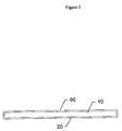
- FIG. 6is a cross section drawing of a completed 4-high stack, ready to be mounted on and connected to an appropriate substrate.
- semiconductor die 10with original connection pads 60 have had an insulating layer applied to the top surface, 30 of all of the die while the die are still connected together in a wafer form.
- a metal layeris deposited and defined using photolithography, to reroute the electrical signals from the original connection pads 60 to new locations at the edge of the die.
- An additional layer of insulating materialis optionally applied above the metal layer, and openings are made in the top layer of insulating material at the relocated pad locations at the edge of the semiconductor die, and optionally at the original pad locations down the center of the top surface of the die.
- the semiconductor die, 10has been thinned by grinding or lapping, and has been singulated from the semiconductor wafer, and said semiconductor die has been coated with a conformal insulating coating 20 .
- openingshave been made in the coating, 20 , above original connection pads, 60 , of semiconductor die, 10 .
- thisshows a semiconductor die 70 with connection pads 80 located around the periphery of the die top surface.
- thisshows openings in the conformal coating material at locations 90 on a semiconductor die whose electrical connections are located at the edges of the surface of the die.
- FIG. 6depicts the vertical stack assembly component 5 , consisting of semiconductor die 10 , with conformal coating 20 .
- the semiconductor die 10having metallic conducting elements 60 , one end of which are connected to electrical connection points at the periphery of the die 10 , and the other end of the metallic conducting elements are embedded in the vertical conducting polymer 50 .
- the vertical conductive polymer 50is adjacent to the edge of the stack of the die and electrically connects the die to the top electrical conducting surface, 94 , on the substrate 7 .
- the epoxy perform 30used to laminate the die 10 to each other in a stack by bonding to the conformal coating 20 on each of the die.
- FIG. 6shows the stack of die 10 laminated to each other with epoxy perform 30 , and connected electrically by horizontal conducting elements 60 to vertical conducting element Vertical conducting elements 50 extend past the bottom of the die stack and are available for electrical and physical attachment to a substrate upon which the die stack will be mounted.
- the present inventioncan comprise a stack of semiconductor or integrated circuit die laminated to each other.
- the diecan optionally have one or more metal rerouting layers to interconnect the original die connection pads with new connection locations at the edge of the top surface of the die.
- the new connection locationsare desirable for vertical interconnection.
- the diecan have a conformal, insulating coating, where the coating can be a polymer.
- the polymer coatingcan parylene, and the insulating coating can have openings above specific new connection locations at the edge of the top surface of the die as required by the specific component design.
- the openingscan be made by preventing the deposition of the polymer coating in selective areas above connection pads on the die.
- the diecan be laminated on top of each other with an electrically insulating polymer or epoxy preform.
- the insulating preformcan be thermally conductive.
- the insulating preformoptionally can include spheres to maintain a fixed spacing or separation between the semiconductor die after lamination.
- the spherescan be made of glass, ceramic, quartz, plastic, Teflon, polymer, or having a metal coating.
- the electrically insulating polymercan consist of epoxy, where the die can be any semiconductor die, such as memory die, where the memory die can be SDRAM, DDR-1, DDR-2, DDR-3, or any other DRAM.
- the memory diecan be NAND Flash, NOR Flash, M-RAM, F-RAM, E2 or any other Non-Volatile Memory.
- the memory diecan be SRAM.
- the stackcan be electrically connected vertically, where the vertical electrical connection comprises a conductive polymer.
- the conductive polymercan be a conductive epoxy, such as silver filled (having particles of silver mixed with the polymer), gold filled (having particles of gold mixed with the polymer), the conductive epoxy being filled with metallic particles (having particles of metal mixed with the polymer).
- connection padscan be “gang-bonded” simultaneously to the connection pads on the die.
- the electrical connectionscan be used selectively to program, or route unique signals to unique layers of semiconductor die within the stack of semiconductor die as required by the specific component design.
- the electrical connectionscan be connected to the corresponding connection on one or more other die in the stack to connect signals of each of the semiconductor die in the stack in common, as required by the specific component design.
- the electrical connectionscan be fanned out so the similar electrical connections from different die in the stack are available at separate, unique connection points on the module (in other words “not in common”).
- the assemblycan optionally be without any additional coating, molding, or covering over the die, and vertical connections.
- the top die of the assemblycan be covered with a material to block or attenuate light from impinging on and affecting the semiconductor die in the assembly.
- the assemblycan be coated with a conformal polymer, such as parylene, where the conformal coating can be the final coating of the device.
- the assemblycan be over-molded with a polymer, plastic, or epoxy to completely coat and cover the stack of semiconductor die, leaving the connections that extend at the bottom of the substrate uncovered and exposed for electrical connection.
- the stacked die assemblyis suitable for high speed circuitry due to the component having low inductance, low capacitance, low DC resistance, and/or matched AC Impedance.
- the componentoptionally can have ground and power planes included in the substrate and or the die.
Landscapes
- Engineering & Computer Science (AREA)
- Power Engineering (AREA)
- Microelectronics & Electronic Packaging (AREA)
- Physics & Mathematics (AREA)
- Condensed Matter Physics & Semiconductors (AREA)
- General Physics & Mathematics (AREA)
- Computer Hardware Design (AREA)
- Encapsulation Of And Coatings For Semiconductor Or Solid State Devices (AREA)
- Wire Bonding (AREA)
- Internal Circuitry In Semiconductor Integrated Circuit Devices (AREA)
- Die Bonding (AREA)
Abstract
Description
- The present application is related to provisional patent application No. 60/561,848, filed Apr. 13, 2004 entitled A HIGH DENSITY LOW PARASITIC STACKED DIE MICROPEDE COMPONENT, the details of which are hereby incorporated by reference, and the benefit of the earlier Apr. 13, 2004 filing date is claimed in accordance with 35 USC 119 (e) (1).
- The present invention relates to an apparatus for stacking and interconnecting integrated circuit die and/or multiple die segments of silicon, and interconnecting the die and or multiple die segments on the edges of the stack using an electrically conductive polymer or epoxy.
- For many years, electrical components such as transistors and integrated circuits have been made using wafers of semiconductor material, including silicon and/or germanium. Integrated circuits have been provided on the wafer using various techniques known as etching, doping, and layering. Individual integrated circuits that are provided on the wafer are referred to as die, and include contact points called bond pads for external electrical connections. Typically, the die on the wafer are separated from one another by cutting the wafer along boundaries defining the die. Once the die are cut from the wafer, they are referred to as chips or die, and are packaged for use. In recent years, the proliferation of more powerful electronic systems has led to an increased need for higher performance and higher density integrated circuit packages.
- One method for creating higher density packages attempts to create an entire computer system on a single wafer using wafer scale integration (WSI) techniques. WSI technology attempts to laterally wire together all the die on a wafer using wires to interconnect the die. However, in order to create the necessary interconnections between the die, many wires are required that are extremely thin and difficult to create. Furthermore, the resulting interconnected die occupy a very large area, or footprint, on the electronic systems circuit board onto which the wafer scale integration device is attached for connection into the electronic system.
- A second method for creating higher density packages attempts to reduce the area required for placing the chips on a circuit board by physically stacking the chips vertically. One chip stacking technique mounts individual die on ceramic carriers, encapsulates both the die and the carrier, stacks the carriers, and then mounts the stack on a printed circuit board. In this technique, all the die in the stack are interconnected by connecting the leads of the die to the printed circuit board via metal pins. This method results in an unusually high pin count on the circuit board which reduces the reliability of the circuitry because the high pin count increases the possibility that one of the many pins may become disconnected from the board.
- Another chip stacking method uses a more complex process to stack die, as disclosed in U.S. Pat. No. 5,104,820 issued Apr. 14, 1992. This method modifies individual chips so that they may be stacked by adding a pattern of metalization, called rerouting leads, to the surface of the wafer. The rerouting leads extend from the bond pads on the chip to newly formed bond pads, and are arranged so that all the rerouting leads terminate on one side of the modified chip. Each modified chip is then cut from the wafer, and assembled into a stack. The stack is assembled in a manner such that all the leads of the modified chips are aligned along the same side of the stack. The side of the stack having the leads is then etched and polished so that a cross section of the leads on each of the modified chips is accessible. After the leads are exposed, a layer of metalization is applied to the leads along the side of the stack in order to electrically connect each of the modified chips in the stack. The stack is then mounted and connected to a substrate which in turn is connected to conventional circuitry.
- This method of rerouting leads offers improvement in circuit density over prior methods but is complex and expensive. In addition, the rerouting leads extend over adjacent die, which are destroyed when the modified chip is cut out of the wafer. In this method, multiple die are sacrificed for every chip that is modified.
- Another method for creating higher density circuits creates stacks from entire wafers, rather than individual chips, to form a wafer array. In some devices, the wafers in the stack are electrically interconnected using solid vertical columns of metallic conductive feed-throughs, such as copper. The use of solid feed-throughs to interconnect wafers may cause damage to the array due to differential thermal coefficients of expansion during thermal cycles. Furthermore, the process is costly and makes the wafers difficult to separate for repairs.
- Other methods also exist to interconnect stacks of wafers, as disclosed in, for example, U.S. Pat. No. 4,897,708 issued Jun. 30, 1990, and U.S. Pat. No. 4,954,875 issued Sep. 4, 1990. These methods provide each wafer in the stack with coned-shaped through-holes which expose bonding pads on the wafers. The bond pads of the wafers in the stack are then electrically connected by either filling the through holes with electrically conductive liquid, or inserting an electrically conductive compliant material into the through holes, to provide a continuous vertical electrical connection between the wafers. While avoiding the disadvantages of using solid vertical columns of metal to interconnect wafers, the use of electrically conductive liquids and conductive materials requires special tooling to fill the through holes. Furthermore, for some applications, it may not be desirable to use stacks of entire wafers due to size constraints of the electrical device.
- Individual semiconductor die are typically assembled in packages that allow the integrated circuit die to be attached to printed circuit boards and to allow electrical connections to be made between the integrated circuit die. There are many types of packages that are used for this purpose. The BGA package and the TSOP package are 2 types of packages in common use for assembling memory die and mounting the assembled die on a printed circuit board. There are a number of methods for stacking packaged integrated circuits, but in general, they suffer from a size disadvantage, and a performance disadvantage, due to the added electrical parasitics arising from the necessary lengths and characteristics of the inter-package interconnections. Due to the large physical size of the packages, there is a limit to the number of packages which may be stacked on top of each other, typically 2, to avoid thermo-mechanical problems. Stacks of packaged integrated circuits have been recently popular but take up too much board space, are too thick, and will not operate at the high speeds being required by advanced memory devices such as DDR2 and DDR3 DRAM.
- Accordingly, it is an object of the present invention to provide an improved method and apparatus for stacking and interconnecting integrated circuit die and multiple die segments.
- The present invention provides an apparatus for vertically interconnecting semiconductor die, integrated circuit die, or multiple die segments. Metal rerouting interconnects which extend to one or more sides of the die or segment can be optionally added to the die or multi die segment to provide edge bonding pads upon the surface of the die for external electrical connection points. After the metal rerouting interconnect has been added to the die on the wafer, the wafer is optionally thinned and each die or multiple die segment is singulated from the wafer by cutting or other appropriate singulation method. After the die or multiple die segments are singulated or cut from the wafer, insulation is applied to all surfaces of the die or multiple die segments, openings are made in the insulation above the desired electrical connection pads, and the die or multiple die segments are placed on top of one another to form a stack. Vertically adjacent segments in the stack are electrically interconnected by attaching a short flexible bond wire or bond ribbon to the exposed electrical connection pad at the peripheral edges of the die which protrudes horizontally from the die and applying electrically conductive polymer, or epoxy, filaments or lines to one or more sides of the stack.
- According to a further aspect of the present invention, a thermally conductive epoxy preformed sheet is provided so that the stack of segments are epoxied together. The thermally conductive epoxy preform includes a plurality of glass spheres randomly distributed within the preform.
- Other objects, features and advantages of the present invention will become apparent from the following detailed description when taken in conjunction with the accompanying drawings.
FIG. 1 is a diagram illustrating a single semiconductor die with original connection pads running down the center of the die, and rerouting lines connecting the original connection pads at the center of the die with new connection pads located at the edges of the die.FIG. 2 is a diagram illustrating a cross sectional side view of a semiconductor die showing the die coated with a conformal, insulating coating.FIG. 3 is a diagram illustrating a cross section view of the semiconductor die showing the conformal coating and openings in the conformal coating above the original connection pads which run down the center of the semiconductor die.FIG. 4 shows a semiconductor die with connection pads around the periphery of the die.FIG. 5 shows a semiconductor die with peripheral pads, either original or relocated, coated with a conformal insulative coating, and with openings in the insulative coating located above the peripherally located electrical connection pads.FIG. 6 is a cross section drawing of a completed 4-high stack, ready to be mounted on and connected to an appropriate substrate.- Referring to
FIG. 1 , semiconductor die10, withoriginal connection pads 60 have had an insulating layer applied to the top surface,30 of all of the die while the die are still connected together in a wafer form. A metal layer is deposited and defined using photolithography, to reroute the electrical signals from theoriginal connection pads 60 to new locations at the edge of the die. An additional layer of insulating material is optionally applied above the metal layer, and openings are made in the top layer of insulating material at the relocated pad locations at the edge of the semiconductor die, and optionally at the original pad locations down the center of the top surface of the die. - Referring to
FIG. 2 , the semiconductor die,10, has been thinned by grinding or lapping, and has been singulated from the semiconductor wafer, and said semiconductor die has been coated with a conformal insulatingcoating 20. - Referring to
FIG. 3 , openings have been made in the coating,20, above original connection pads,60, of semiconductor die,10. - Referring to
FIG. 4 , this shows asemiconductor die 70 withconnection pads 80 located around the periphery of the die top surface. - Referring to
FIG. 5 , this shows openings in the conformal coating material atlocations 90 on a semiconductor die whose electrical connections are located at the edges of the surface of the die. FIG. 6 depicts the verticalstack assembly component 5, consisting of semiconductor die10, withconformal coating 20. The semiconductor die10 having metallic conductingelements 60, one end of which are connected to electrical connection points at the periphery of the die10, and the other end of the metallic conducting elements are embedded in the vertical conductingpolymer 50. The verticalconductive polymer 50 is adjacent to the edge of the stack of the die and electrically connects the die to the top electrical conducting surface,94, on the substrate7.- Also shown in
FIG. 6 is the epoxy perform30 used to laminate the die10 to each other in a stack by bonding to theconformal coating 20 on each of the die. FIG. 6 shows the stack of die10 laminated to each other withepoxy perform 30, and connected electrically byhorizontal conducting elements 60 to vertical conducting elementVertical conducting elements 50 extend past the bottom of the die stack and are available for electrical and physical attachment to a substrate upon which the die stack will be mounted.- The foregoing has described a high density, low parasitic stacked die assembly. It should be apparent that numerous and various components can be utilized with the present invention, as described below.
- For instance, the present invention can comprise a stack of semiconductor or integrated circuit die laminated to each other. The die can optionally have one or more metal rerouting layers to interconnect the original die connection pads with new connection locations at the edge of the top surface of the die. The new connection locations are desirable for vertical interconnection.
- The die can have a conformal, insulating coating, where the coating can be a polymer. The polymer coating can parylene, and the insulating coating can have openings above specific new connection locations at the edge of the top surface of the die as required by the specific component design.
- The openings can be made, for example, by removing the polymer with laser ablation, and by removing the polymer with a plasma etcher.
- The openings can be made by preventing the deposition of the polymer coating in selective areas above connection pads on the die. The die can be laminated on top of each other with an electrically insulating polymer or epoxy preform. The insulating preform can be thermally conductive.
- The insulating preform optionally can include spheres to maintain a fixed spacing or separation between the semiconductor die after lamination. The spheres can be made of glass, ceramic, quartz, plastic, Teflon, polymer, or having a metal coating.
- The electrically insulating polymer can be an epoxy. The die can be laminated on top of each other with a liquid polymer that is cured to form a solid bond between the layers in the stack. The insulating polymer can optionally include spheres to maintain a fixed spacing or separation between the semiconductor die after lamination, where the spheres can be made of glass, ceramic, quartz, plastic, Teflon, a polymer, and/or a metal coating.
- The electrically insulating polymer can consist of epoxy, where the die can be any semiconductor die, such as memory die, where the memory die can be SDRAM, DDR-1, DDR-2, DDR-3, or any other DRAM. The memory die can be NAND Flash, NOR Flash, M-RAM, F-RAM, E2 or any other Non-Volatile Memory. The memory die can be SRAM.
- The stack can be electrically connected vertically, where the vertical electrical connection comprises a conductive polymer. The conductive polymer can be a conductive epoxy, such as silver filled (having particles of silver mixed with the polymer), gold filled (having particles of gold mixed with the polymer), the conductive epoxy being filled with metallic particles (having particles of metal mixed with the polymer).
- The electrical connection can include one or more metallic conducting elements bonded to the relocated pad locations on the surface of each die and extending, both physically and electrically from the relocated pad into the vertical conductor so that one end of the conductor is embedded within the conductive polymer. The metallic conducting elements can be a bond wire, bond ribbon. The metallic conducting element can be gold, aluminum, copper, or palladium, on any combination of conducting materials such as gold, aluminum, copper, or palladium. The metallic conducting elements can exist as a metal lead frame with tie bars which is bonded to the die, and after which the tie bars of metal are removed to leave individual metal conducting elements or leads bonded to the connection pads on the die. The frame can be formed by excising holes in a thin plate of metal. The frame can be cut to remove a center ring or picture frame, leaving behind metal leads ready to attach to the bonding pads on the die, or the frame can be cut to remove an outer ring or picture frame after the leads have been bonded to the connection pads on the die.
- All of the connection pads can be “gang-bonded” simultaneously to the connection pads on the die. The electrical connections can be used selectively to program, or route unique signals to unique layers of semiconductor die within the stack of semiconductor die as required by the specific component design. The electrical connections can be connected to the corresponding connection on one or more other die in the stack to connect signals of each of the semiconductor die in the stack in common, as required by the specific component design. The electrical connections can be fanned out so the similar electrical connections from different die in the stack are available at separate, unique connection points on the module (in other words “not in common”).
- The assembly can optionally be without any additional coating, molding, or covering over the die, and vertical connections. The top die of the assembly can be covered with a material to block or attenuate light from impinging on and affecting the semiconductor die in the assembly. The assembly can be coated with a conformal polymer, such as parylene, where the conformal coating can be the final coating of the device.
- The assembly can be over-molded with a polymer, plastic, or epoxy to completely coat and cover the stack of semiconductor die, leaving the connections that extend at the bottom of the substrate uncovered and exposed for electrical connection.
- The stacked die assembly is suitable for high speed circuitry due to the component having low inductance, low capacitance, low DC resistance, and/or matched AC Impedance. The component optionally can have ground and power planes included in the substrate and or the die.
Claims (12)
Priority Applications (2)
| Application Number | Priority Date | Filing Date | Title |
|---|---|---|---|
| US11/097,829US7245021B2 (en) | 2004-04-13 | 2005-03-31 | Micropede stacked die component assembly |
| US11/744,153US7535109B2 (en) | 2004-04-13 | 2007-05-03 | Die assembly having electrical interconnect |
Applications Claiming Priority (2)
| Application Number | Priority Date | Filing Date | Title |
|---|---|---|---|
| US56184804P | 2004-04-13 | 2004-04-13 | |
| US11/097,829US7245021B2 (en) | 2004-04-13 | 2005-03-31 | Micropede stacked die component assembly |
Related Child Applications (1)
| Application Number | Title | Priority Date | Filing Date |
|---|---|---|---|
| US11/744,153ContinuationUS7535109B2 (en) | 2004-04-13 | 2007-05-03 | Die assembly having electrical interconnect |
Publications (2)
| Publication Number | Publication Date |
|---|---|
| US20050258530A1true US20050258530A1 (en) | 2005-11-24 |
| US7245021B2 US7245021B2 (en) | 2007-07-17 |
Family
ID=35150639
Family Applications (2)
| Application Number | Title | Priority Date | Filing Date |
|---|---|---|---|
| US11/097,829Expired - Fee RelatedUS7245021B2 (en) | 2004-04-13 | 2005-03-31 | Micropede stacked die component assembly |
| US11/744,153Expired - LifetimeUS7535109B2 (en) | 2004-04-13 | 2007-05-03 | Die assembly having electrical interconnect |
Family Applications After (1)
| Application Number | Title | Priority Date | Filing Date |
|---|---|---|---|
| US11/744,153Expired - LifetimeUS7535109B2 (en) | 2004-04-13 | 2007-05-03 | Die assembly having electrical interconnect |
Country Status (5)
| Country | Link |
|---|---|
| US (2) | US7245021B2 (en) |
| EP (1) | EP1743369A4 (en) |
| KR (1) | KR101233751B1 (en) |
| TW (1) | TWI384598B (en) |
| WO (1) | WO2005101491A2 (en) |
Cited By (36)
| Publication number | Priority date | Publication date | Assignee | Title |
|---|---|---|---|---|
| US7413979B2 (en) | 2003-11-13 | 2008-08-19 | Micron Technology, Inc. | Methods for forming vias in microelectronic devices, and methods for packaging microelectronic devices |
| US7425499B2 (en) | 2004-08-24 | 2008-09-16 | Micron Technology, Inc. | Methods for forming interconnects in vias and microelectronic workpieces including such interconnects |
| US7435913B2 (en) | 2004-08-27 | 2008-10-14 | Micron Technology, Inc. | Slanted vias for electrical circuits on circuit boards and other substrates |
| US20090014859A1 (en)* | 2007-07-12 | 2009-01-15 | Micron Technology, Inc. | Interconnects for packaged semiconductor devices and methods for manufacturing such devices |
| US20090065916A1 (en)* | 2007-09-10 | 2009-03-12 | Vertical Circuits, Inc. | Semiconductor die mount by conformal die coating |
| US7531453B2 (en) | 2004-06-29 | 2009-05-12 | Micron Technology, Inc. | Microelectronic devices and methods for forming interconnects in microelectronic devices |
| US7589008B2 (en) | 2004-12-30 | 2009-09-15 | Micron Technology, Inc. | Methods for forming interconnects in microelectronic workpieces and microelectronic workpieces formed using such methods |
| US7622377B2 (en) | 2005-09-01 | 2009-11-24 | Micron Technology, Inc. | Microfeature workpiece substrates having through-substrate vias, and associated methods of formation |
| US7629249B2 (en) | 2006-08-28 | 2009-12-08 | Micron Technology, Inc. | Microfeature workpieces having conductive interconnect structures formed by chemically reactive processes, and associated systems and methods |
| US20090325322A1 (en)* | 2008-06-25 | 2009-12-31 | Joseph Martin Patterson | Non-Destructive Laser Optical Integrated Circuit Package Marking |
| US7683458B2 (en) | 2004-09-02 | 2010-03-23 | Micron Technology, Inc. | Through-wafer interconnects for photoimager and memory wafers |
| US7749899B2 (en) | 2006-06-01 | 2010-07-06 | Micron Technology, Inc. | Microelectronic workpieces and methods and systems for forming interconnects in microelectronic workpieces |
| US7795134B2 (en) | 2005-06-28 | 2010-09-14 | Micron Technology, Inc. | Conductive interconnect structures and formation methods using supercritical fluids |
| US7830018B2 (en) | 2007-08-31 | 2010-11-09 | Micron Technology, Inc. | Partitioned through-layer via and associated systems and methods |
| US7863187B2 (en) | 2005-09-01 | 2011-01-04 | Micron Technology, Inc. | Microfeature workpieces and methods for forming interconnects in microfeature workpieces |
| US7884015B2 (en) | 2007-12-06 | 2011-02-08 | Micron Technology, Inc. | Methods for forming interconnects in microelectronic workpieces and microelectronic workpieces formed using such methods |
| US7902643B2 (en) | 2006-08-31 | 2011-03-08 | Micron Technology, Inc. | Microfeature workpieces having interconnects and conductive backplanes, and associated systems and methods |
| US7915736B2 (en) | 2005-09-01 | 2011-03-29 | Micron Technology, Inc. | Microfeature workpieces and methods for forming interconnects in microfeature workpieces |
| JP2011514012A (en)* | 2008-03-12 | 2011-04-28 | ヴァーティカル・サーキツツ・インコーポレーテッド | Support attached by electrically interconnecting the die assembly |
| US8084866B2 (en) | 2003-12-10 | 2011-12-27 | Micron Technology, Inc. | Microelectronic devices and methods for filling vias in microelectronic devices |
| US8536485B2 (en) | 2004-05-05 | 2013-09-17 | Micron Technology, Inc. | Systems and methods for forming apertures in microfeature workpieces |
| US8723332B2 (en) | 2007-06-11 | 2014-05-13 | Invensas Corporation | Electrically interconnected stacked die assemblies |
| US8884403B2 (en) | 2008-06-19 | 2014-11-11 | Iinvensas Corporation | Semiconductor die array structure |
| US8912661B2 (en) | 2009-11-04 | 2014-12-16 | Invensas Corporation | Stacked die assembly having reduced stress electrical interconnects |
| US8981574B2 (en) | 2012-12-20 | 2015-03-17 | Samsung Electronics Co., Ltd. | Semiconductor package |
| TWI491007B (en)* | 2007-09-07 | 2015-07-01 | Invensas Corp | Electrical interconnect formed by pulsed dispense |
| US9147583B2 (en) | 2009-10-27 | 2015-09-29 | Invensas Corporation | Selective die electrical insulation by additive process |
| US9153517B2 (en) | 2008-05-20 | 2015-10-06 | Invensas Corporation | Electrical connector between die pad and z-interconnect for stacked die assemblies |
| US9490195B1 (en) | 2015-07-17 | 2016-11-08 | Invensas Corporation | Wafer-level flipped die stacks with leadframes or metal foil interconnects |
| US9508691B1 (en) | 2015-12-16 | 2016-11-29 | Invensas Corporation | Flipped die stacks with multiple rows of leadframe interconnects |
| US9595511B1 (en) | 2016-05-12 | 2017-03-14 | Invensas Corporation | Microelectronic packages and assemblies with improved flyby signaling operation |
| US9728524B1 (en) | 2016-06-30 | 2017-08-08 | Invensas Corporation | Enhanced density assembly having microelectronic packages mounted at substantial angle to board |
| US9825002B2 (en) | 2015-07-17 | 2017-11-21 | Invensas Corporation | Flipped die stack |
| US9871019B2 (en) | 2015-07-17 | 2018-01-16 | Invensas Corporation | Flipped die stack assemblies with leadframe interconnects |
| US10566310B2 (en) | 2016-04-11 | 2020-02-18 | Invensas Corporation | Microelectronic packages having stacked die and wire bond interconnects |
| CN114171504A (en)* | 2020-09-11 | 2022-03-11 | 西部数据技术公司 | Straight wire bonding of silicon die |
Families Citing this family (23)
| Publication number | Priority date | Publication date | Assignee | Title |
|---|---|---|---|---|
| US7245021B2 (en)* | 2004-04-13 | 2007-07-17 | Vertical Circuits, Inc. | Micropede stacked die component assembly |
| US7215018B2 (en)* | 2004-04-13 | 2007-05-08 | Vertical Circuits, Inc. | Stacked die BGA or LGA component assembly |
| US7705432B2 (en)* | 2004-04-13 | 2010-04-27 | Vertical Circuits, Inc. | Three dimensional six surface conformal die coating |
| US7663216B2 (en)* | 2005-11-02 | 2010-02-16 | Sandisk Corporation | High density three dimensional semiconductor die package |
| JP5177625B2 (en)* | 2006-07-11 | 2013-04-03 | 独立行政法人産業技術総合研究所 | Electrode connection structure and conductive member of semiconductor chip, semiconductor device, and manufacturing method thereof |
| US8154881B2 (en)* | 2006-11-13 | 2012-04-10 | Telecommunication Systems, Inc. | Radiation-shielded semiconductor assembly |
| TW200917391A (en)* | 2007-06-20 | 2009-04-16 | Vertical Circuits Inc | Three-dimensional circuitry formed on integrated circuit device using two-dimensional fabrication |
| WO2009026171A2 (en)* | 2007-08-17 | 2009-02-26 | Vertical Circuits, Inc. | Stacked die vertical interconnect formed by transfer of interconnect material |
| WO2009052150A1 (en)* | 2007-10-18 | 2009-04-23 | Vertical Circuits, Inc. | Chip scale stacked die package |
| US7843046B2 (en)* | 2008-02-19 | 2010-11-30 | Vertical Circuits, Inc. | Flat leadless packages and stacked leadless package assemblies |
| US8829677B2 (en) | 2010-10-14 | 2014-09-09 | Invensas Corporation | Semiconductor die having fine pitch electrical interconnects |
| US20100117224A1 (en)* | 2008-08-29 | 2010-05-13 | Vertical Circuits, Inc. | Sensor |
| US8097956B2 (en)* | 2009-03-12 | 2012-01-17 | Apple Inc. | Flexible packaging for chip-on-chip and package-on-package technologies |
| US8533853B2 (en) | 2009-06-12 | 2013-09-10 | Telecommunication Systems, Inc. | Location sensitive solid state drive |
| WO2010151578A2 (en) | 2009-06-26 | 2010-12-29 | Vertical Circuits, Inc. | Electrical interconnect for die stacked in zig-zag configuration |
| US8664748B2 (en)* | 2009-08-17 | 2014-03-04 | Mosaid Technologies Incorporated | Package-level integrated circuit connection without top metal pads or bonding wire |
| US8383949B2 (en)* | 2009-12-29 | 2013-02-26 | Intel Corporation | Method to form lateral pad on edge of wafer |
| US9164886B1 (en) | 2010-09-21 | 2015-10-20 | Western Digital Technologies, Inc. | System and method for multistage processing in a memory storage subsystem |
| US8587088B2 (en) | 2011-02-17 | 2013-11-19 | Apple Inc. | Side-mounted controller and methods for making the same |
| WO2013067270A1 (en) | 2011-11-04 | 2013-05-10 | Invensas Corporation | Bonding wedge |
| KR102099878B1 (en)* | 2013-07-11 | 2020-04-10 | 삼성전자 주식회사 | Semiconductor Package |
| KR20180090494A (en) | 2017-02-03 | 2018-08-13 | 삼성전자주식회사 | Method for fabricating substrate structure |
| CN112151514B (en)* | 2019-06-28 | 2025-07-29 | 桑迪士克科技股份有限公司 | Semiconductor device including vertically stacked semiconductor die |
Citations (69)
| Publication number | Priority date | Publication date | Assignee | Title |
|---|---|---|---|---|
| US511278A (en)* | 1893-12-19 | James s | ||
| US2202289A (en)* | 1939-01-20 | 1940-05-28 | Herr Mfg Co Inc | Flier for spinning machines |
| US3648131A (en)* | 1969-11-07 | 1972-03-07 | Ibm | Hourglass-shaped conductive connection through semiconductor structures |
| US4074342A (en)* | 1974-12-20 | 1978-02-14 | International Business Machines Corporation | Electrical package for lsi devices and assembly process therefor |
| US4323914A (en)* | 1979-02-01 | 1982-04-06 | International Business Machines Corporation | Heat transfer structure for integrated circuit package |
| US4525921A (en)* | 1981-07-13 | 1985-07-02 | Irvine Sensors Corporation | High-density electronic processing package-structure and fabrication |
| US4545840A (en)* | 1983-03-08 | 1985-10-08 | Monolithic Memories, Inc. | Process for controlling thickness of die attach adhesive |
| US4646128A (en)* | 1980-09-16 | 1987-02-24 | Irvine Sensors Corporation | High-density electronic processing package--structure and fabrication |
| US4659931A (en)* | 1985-05-08 | 1987-04-21 | Grumman Aerospace Corporation | High density multi-layered integrated circuit package |
| US4672737A (en)* | 1984-01-23 | 1987-06-16 | Irvine Sensors Corporation | Detector array module fabrication process |
| US4703170A (en)* | 1985-04-12 | 1987-10-27 | Grumman Aerospace Corporation | Infrared focal plane module |
| US4706166A (en)* | 1986-04-25 | 1987-11-10 | Irvine Sensors Corporation | High-density electronic modules--process and product |
| US4761681A (en)* | 1982-09-08 | 1988-08-02 | Texas Instruments Incorporated | Method for fabricating a semiconductor contact and interconnect structure using orientation dependent etching and thermomigration |
| US4764846A (en)* | 1987-01-05 | 1988-08-16 | Irvine Sensors Corporation | High density electronic package comprising stacked sub-modules |
| US4818823A (en)* | 1987-07-06 | 1989-04-04 | Micro-Circuits, Inc. | Adhesive component means for attaching electrical components to conductors |
| US4862249A (en)* | 1987-04-17 | 1989-08-29 | Xoc Devices, Inc. | Packaging system for stacking integrated circuits |
| US4894706A (en)* | 1985-02-14 | 1990-01-16 | Nippon Telegraph And Telephone Corporation | Three-dimensional packaging of semiconductor device chips |
| US4897708A (en)* | 1986-07-17 | 1990-01-30 | Laser Dynamics, Inc. | Semiconductor wafer array |
| US4939588A (en)* | 1987-08-14 | 1990-07-03 | Fuji Photo Film Co., Ltd. | Electronic copying machine |
| US4941033A (en)* | 1988-12-27 | 1990-07-10 | Mitsubishi Denki Kabushiki Kaisha | Semiconductor integrated circuit device |
| US4954875A (en)* | 1986-07-17 | 1990-09-04 | Laser Dynamics, Inc. | Semiconductor wafer array with electrically conductive compliant material |
| US4956594A (en)* | 1987-09-19 | 1990-09-11 | Fanuc Ltd. | Method of controlling a robot in accordance with load conditions |
| US4956695A (en)* | 1989-05-12 | 1990-09-11 | Rockwell International Corporation | Three-dimensional packaging of focal plane assemblies using ceramic spacers |
| US4959749A (en)* | 1989-08-16 | 1990-09-25 | Unisys Corporation | Layered electronic assembly having compensation for chips of different thickness and different I/O lead offsets |
| US4983533A (en)* | 1987-10-28 | 1991-01-08 | Irvine Sensors Corporation | High-density electronic modules - process and product |
| US4996583A (en)* | 1989-02-15 | 1991-02-26 | Matsushita Electric Industrial Co., Ltd. | Stack type semiconductor package |
| US5013687A (en)* | 1989-07-27 | 1991-05-07 | Grumman Aerospace Corporation | Framed chip hybrid stacked layer assembly |
| US5019943A (en)* | 1990-02-14 | 1991-05-28 | Unisys Corporation | High density chip stack having a zigzag-shaped face which accommodates connections between chips |
| US5025306A (en)* | 1988-08-09 | 1991-06-18 | Texas Instruments Incorporated | Assembly of semiconductor chips |
| US5028986A (en)* | 1987-12-28 | 1991-07-02 | Hitachi, Ltd. | Semiconductor device and semiconductor module with a plurality of stacked semiconductor devices |
| US5075253A (en)* | 1989-04-12 | 1991-12-24 | Advanced Micro Devices, Inc. | Method of coplanar integration of semiconductor IC devices |
| US5093708A (en)* | 1990-08-20 | 1992-03-03 | Grumman Aerospace Corporation | Multilayer integrated circuit module |
| US5104820A (en)* | 1989-07-07 | 1992-04-14 | Irvine Sensors Corporation | Method of fabricating electronic circuitry unit containing stacked IC layers having lead rerouting |
| US5117282A (en)* | 1990-10-29 | 1992-05-26 | Harris Corporation | Stacked configuration for integrated circuit devices |
| US5146308A (en)* | 1990-10-05 | 1992-09-08 | Micron Technology, Inc. | Semiconductor package utilizing edge connected semiconductor dice |
| US5191405A (en)* | 1988-12-23 | 1993-03-02 | Matsushita Electric Industrial Co., Ltd. | Three-dimensional stacked lsi |
| US5198888A (en)* | 1987-12-28 | 1993-03-30 | Hitachi, Ltd. | Semiconductor stacked device |
| US5202754A (en)* | 1991-09-13 | 1993-04-13 | International Business Machines Corporation | Three-dimensional multichip packages and methods of fabrication |
| US5229647A (en)* | 1991-03-27 | 1993-07-20 | Micron Technology, Inc. | High density data storage using stacked wafers |
| US5231304A (en)* | 1989-07-27 | 1993-07-27 | Grumman Aerospace Corporation | Framed chip hybrid stacked layer assembly |
| US5247423A (en)* | 1992-05-26 | 1993-09-21 | Motorola, Inc. | Stacking three dimensional leadless multi-chip module and method for making the same |
| US5270261A (en)* | 1991-09-13 | 1993-12-14 | International Business Machines Corporation | Three dimensional multichip package methods of fabrication |
| US5279029A (en)* | 1990-08-01 | 1994-01-18 | Staktek Corporation | Ultra high density integrated circuit packages method |
| US5311401A (en)* | 1991-07-09 | 1994-05-10 | Hughes Aircraft Company | Stacked chip assembly and manufacturing method therefor |
| US5313096A (en)* | 1992-03-16 | 1994-05-17 | Dense-Pac Microsystems, Inc. | IC chip package having chip attached to and wire bonded within an overlying substrate |
| US5330359A (en)* | 1993-03-26 | 1994-07-19 | The Whitaker Corporation | Socket for stacking integrated circuit chips |
| US5422435A (en)* | 1992-05-22 | 1995-06-06 | National Semiconductor Corporation | Stacked multi-chip modules and method of manufacturing |
| US5434745A (en)* | 1994-07-26 | 1995-07-18 | White Microelectronics Div. Of Bowmar Instrument Corp. | Stacked silicon die carrier assembly |
| US5445994A (en)* | 1994-04-11 | 1995-08-29 | Micron Technology, Inc. | Method for forming custom planar metal bonding pad connectors for semiconductor dice |
| US5446620A (en)* | 1990-08-01 | 1995-08-29 | Staktek Corporation | Ultra high density integrated circuit packages |
| US5493476A (en)* | 1994-03-07 | 1996-02-20 | Staktek Corporation | Bus communication system for stacked high density integrated circuit packages with bifurcated distal lead ends |
| US5499160A (en)* | 1990-08-01 | 1996-03-12 | Staktek Corporation | High density integrated circuit module with snap-on rail assemblies |
| US5502333A (en)* | 1994-03-30 | 1996-03-26 | International Business Machines Corporation | Semiconductor stack structures and fabrication/sparing methods utilizing programmable spare circuit |
| US5600541A (en)* | 1993-12-08 | 1997-02-04 | Hughes Aircraft Company | Vertical IC chip stack with discrete chip carriers formed from dielectric tape |
| US5625230A (en)* | 1994-12-28 | 1997-04-29 | Samsung Display Devices Co., Ltd. | Integrated circuit chip structure |
| US5657206A (en)* | 1994-06-23 | 1997-08-12 | Cubic Memory, Inc. | Conductive epoxy flip-chip package and method |
| US5675180A (en)* | 1994-06-23 | 1997-10-07 | Cubic Memory, Inc. | Vertical interconnect process for silicon segments |
| US5688721A (en)* | 1994-03-15 | 1997-11-18 | Irvine Sensors Corporation | 3D stack of IC chips having leads reached by vias through passivation covering access plane |
| US5696031A (en)* | 1996-11-20 | 1997-12-09 | Micron Technology, Inc. | Device and method for stacking wire-bonded integrated circuit dice on flip-chip bonded integrated circuit dice |
| US5698895A (en)* | 1994-06-23 | 1997-12-16 | Cubic Memory, Inc. | Silicon segment programming method and apparatus |
| US5724230A (en)* | 1996-06-21 | 1998-03-03 | International Business Machines Corporation | Flexible laminate module including spacers embedded in an adhesive |
| US5891761A (en)* | 1994-06-23 | 1999-04-06 | Cubic Memory, Inc. | Method for forming vertical interconnect process for silicon segments with thermally conductive epoxy preform |
| US6080596A (en)* | 1994-06-23 | 2000-06-27 | Cubic Memory Inc. | Method for forming vertical interconnect process for silicon segments with dielectric isolation |
| US6124633A (en)* | 1994-06-23 | 2000-09-26 | Cubic Memory | Vertical interconnect process for silicon segments with thermally conductive epoxy preform |
| US6255726B1 (en)* | 1994-06-23 | 2001-07-03 | Cubic Memory, Inc. | Vertical interconnect process for silicon segments with dielectric isolation |
| US6271598B1 (en)* | 1997-07-29 | 2001-08-07 | Cubic Memory, Inc. | Conductive epoxy flip-chip on chip |
| US20020180010A1 (en)* | 1996-11-21 | 2002-12-05 | Kunihiro Tsubosaki | Semiconductor device and manufacturing method thereof |
| US20040238933A1 (en)* | 2003-05-27 | 2004-12-02 | Shou-Lung Chen | Stacked package for electronic elements and packaging method thereof |
| US6973718B2 (en)* | 2001-05-30 | 2005-12-13 | Microchips, Inc. | Methods for conformal coating and sealing microchip reservoir devices |
Family Cites Families (22)
| Publication number | Priority date | Publication date | Assignee | Title |
|---|---|---|---|---|
| KR900008647B1 (en) | 1986-03-20 | 1990-11-26 | 후지쓰 가부시끼가이샤 | A method for manufacturing three demensional i.c. |
| JPH0680878B2 (en) | 1986-08-27 | 1994-10-12 | 日本電気株式会社 | Integrated circuit |
| US5138437A (en)* | 1987-07-27 | 1992-08-11 | Mitsubishi Denki Kabushiki Kaisha | Semiconductor integrated circuit device in which integrated circuit units having different functions are stacked in three dimensional manner |
| JPS6435528A (en) | 1987-07-31 | 1989-02-06 | Optrex Kk | Terminal connecting structure |
| JPS6435528U (en) | 1987-08-22 | 1989-03-03 | ||
| US4956694A (en) | 1988-11-04 | 1990-09-11 | Dense-Pac Microsystems, Inc. | Integrated circuit chip stacking |
| JPH02133936A (en) | 1988-11-15 | 1990-05-23 | Seiko Epson Corp | semiconductor equipment |
| US5258330A (en)* | 1990-09-24 | 1993-11-02 | Tessera, Inc. | Semiconductor chip assemblies with fan-in leads |
| US5172303A (en)* | 1990-11-23 | 1992-12-15 | Motorola, Inc. | Electronic component assembly |
| US5111278A (en) | 1991-03-27 | 1992-05-05 | Eichelberger Charles W | Three-dimensional multichip module systems |
| US5135556A (en)* | 1991-04-08 | 1992-08-04 | Grumman Aerospace Corporation | Method for making fused high density multi-layer integrated circuit module |
| US5221642A (en)* | 1991-08-15 | 1993-06-22 | Staktek Corporation | Lead-on-chip integrated circuit fabrication method |
| US5270571A (en)* | 1991-10-30 | 1993-12-14 | Amdahl Corporation | Three-dimensional package for semiconductor devices |
| JPH05160290A (en)* | 1991-12-06 | 1993-06-25 | Rohm Co Ltd | Circuit module |
| US5222014A (en)* | 1992-03-02 | 1993-06-22 | Motorola, Inc. | Three-dimensional multi-chip pad array carrier |
| WO1993023982A1 (en) | 1992-05-11 | 1993-11-25 | Nchip, Inc. | Stacked devices for multichip modules |
| EP1029360A4 (en) | 1997-08-21 | 2006-04-12 | Vertical Circuits Inc | VERTICAL INTERMEDIATE CONNECTION METHOD FOR SILICON SEGMENTS WITH DIELECTRIC INSULATION |
| US6153929A (en)* | 1998-08-21 | 2000-11-28 | Micron Technology, Inc. | Low profile multi-IC package connector |
| JP2001223323A (en)* | 2000-02-10 | 2001-08-17 | Mitsubishi Electric Corp | Semiconductor device |
| ES2420279T3 (en) | 2000-03-02 | 2013-08-23 | Microchips, Inc. | Microfabricated devices and methods for storage and selective exposure of chemicals |
| US7215018B2 (en)* | 2004-04-13 | 2007-05-08 | Vertical Circuits, Inc. | Stacked die BGA or LGA component assembly |
| US7245021B2 (en)* | 2004-04-13 | 2007-07-17 | Vertical Circuits, Inc. | Micropede stacked die component assembly |
- 2005
- 2005-03-31USUS11/097,829patent/US7245021B2/ennot_activeExpired - Fee Related
- 2005-04-11TWTW094111359Apatent/TWI384598B/ennot_activeIP Right Cessation
- 2005-04-12WOPCT/US2005/012394patent/WO2005101491A2/enactiveApplication Filing
- 2005-04-12KRKR1020067023770Apatent/KR101233751B1/ennot_activeExpired - Fee Related
- 2005-04-12EPEP05735136Apatent/EP1743369A4/ennot_activeWithdrawn
- 2007
- 2007-05-03USUS11/744,153patent/US7535109B2/ennot_activeExpired - Lifetime
Patent Citations (78)
| Publication number | Priority date | Publication date | Assignee | Title |
|---|---|---|---|---|
| US511278A (en)* | 1893-12-19 | James s | ||
| US2202289A (en)* | 1939-01-20 | 1940-05-28 | Herr Mfg Co Inc | Flier for spinning machines |
| US3648131A (en)* | 1969-11-07 | 1972-03-07 | Ibm | Hourglass-shaped conductive connection through semiconductor structures |
| US4074342A (en)* | 1974-12-20 | 1978-02-14 | International Business Machines Corporation | Electrical package for lsi devices and assembly process therefor |
| US4323914A (en)* | 1979-02-01 | 1982-04-06 | International Business Machines Corporation | Heat transfer structure for integrated circuit package |
| US4646128A (en)* | 1980-09-16 | 1987-02-24 | Irvine Sensors Corporation | High-density electronic processing package--structure and fabrication |
| US4525921A (en)* | 1981-07-13 | 1985-07-02 | Irvine Sensors Corporation | High-density electronic processing package-structure and fabrication |
| US4761681A (en)* | 1982-09-08 | 1988-08-02 | Texas Instruments Incorporated | Method for fabricating a semiconductor contact and interconnect structure using orientation dependent etching and thermomigration |
| US4545840A (en)* | 1983-03-08 | 1985-10-08 | Monolithic Memories, Inc. | Process for controlling thickness of die attach adhesive |
| US4672737A (en)* | 1984-01-23 | 1987-06-16 | Irvine Sensors Corporation | Detector array module fabrication process |
| US4894706A (en)* | 1985-02-14 | 1990-01-16 | Nippon Telegraph And Telephone Corporation | Three-dimensional packaging of semiconductor device chips |
| US4703170A (en)* | 1985-04-12 | 1987-10-27 | Grumman Aerospace Corporation | Infrared focal plane module |
| US4659931A (en)* | 1985-05-08 | 1987-04-21 | Grumman Aerospace Corporation | High density multi-layered integrated circuit package |
| US4706166A (en)* | 1986-04-25 | 1987-11-10 | Irvine Sensors Corporation | High-density electronic modules--process and product |
| US4954875A (en)* | 1986-07-17 | 1990-09-04 | Laser Dynamics, Inc. | Semiconductor wafer array with electrically conductive compliant material |
| US4897708A (en)* | 1986-07-17 | 1990-01-30 | Laser Dynamics, Inc. | Semiconductor wafer array |
| US4764846A (en)* | 1987-01-05 | 1988-08-16 | Irvine Sensors Corporation | High density electronic package comprising stacked sub-modules |
| US4862249A (en)* | 1987-04-17 | 1989-08-29 | Xoc Devices, Inc. | Packaging system for stacking integrated circuits |
| US4818823A (en)* | 1987-07-06 | 1989-04-04 | Micro-Circuits, Inc. | Adhesive component means for attaching electrical components to conductors |
| US4939588A (en)* | 1987-08-14 | 1990-07-03 | Fuji Photo Film Co., Ltd. | Electronic copying machine |
| US4956594A (en)* | 1987-09-19 | 1990-09-11 | Fanuc Ltd. | Method of controlling a robot in accordance with load conditions |
| US4983533A (en)* | 1987-10-28 | 1991-01-08 | Irvine Sensors Corporation | High-density electronic modules - process and product |
| US5028986A (en)* | 1987-12-28 | 1991-07-02 | Hitachi, Ltd. | Semiconductor device and semiconductor module with a plurality of stacked semiconductor devices |
| US5198888A (en)* | 1987-12-28 | 1993-03-30 | Hitachi, Ltd. | Semiconductor stacked device |
| US5025306A (en)* | 1988-08-09 | 1991-06-18 | Texas Instruments Incorporated | Assembly of semiconductor chips |
| US5191405A (en)* | 1988-12-23 | 1993-03-02 | Matsushita Electric Industrial Co., Ltd. | Three-dimensional stacked lsi |
| US4941033A (en)* | 1988-12-27 | 1990-07-10 | Mitsubishi Denki Kabushiki Kaisha | Semiconductor integrated circuit device |
| US4996583A (en)* | 1989-02-15 | 1991-02-26 | Matsushita Electric Industrial Co., Ltd. | Stack type semiconductor package |
| US5075253A (en)* | 1989-04-12 | 1991-12-24 | Advanced Micro Devices, Inc. | Method of coplanar integration of semiconductor IC devices |
| US4956695A (en)* | 1989-05-12 | 1990-09-11 | Rockwell International Corporation | Three-dimensional packaging of focal plane assemblies using ceramic spacers |
| US5104820A (en)* | 1989-07-07 | 1992-04-14 | Irvine Sensors Corporation | Method of fabricating electronic circuitry unit containing stacked IC layers having lead rerouting |
| US5013687A (en)* | 1989-07-27 | 1991-05-07 | Grumman Aerospace Corporation | Framed chip hybrid stacked layer assembly |
| US5231304A (en)* | 1989-07-27 | 1993-07-27 | Grumman Aerospace Corporation | Framed chip hybrid stacked layer assembly |
| US4959749A (en)* | 1989-08-16 | 1990-09-25 | Unisys Corporation | Layered electronic assembly having compensation for chips of different thickness and different I/O lead offsets |
| US5019943A (en)* | 1990-02-14 | 1991-05-28 | Unisys Corporation | High density chip stack having a zigzag-shaped face which accommodates connections between chips |
| US5566051A (en)* | 1990-08-01 | 1996-10-15 | Staktek Corporation | Ultra high density integrated circuit packages method and apparatus |
| US5420751A (en)* | 1990-08-01 | 1995-05-30 | Staktek Corporation | Ultra high density modular integrated circuit package |
| US5550711A (en)* | 1990-08-01 | 1996-08-27 | Staktek Corporation | Ultra high density integrated circuit packages |
| US5499160A (en)* | 1990-08-01 | 1996-03-12 | Staktek Corporation | High density integrated circuit module with snap-on rail assemblies |
| US5279029A (en)* | 1990-08-01 | 1994-01-18 | Staktek Corporation | Ultra high density integrated circuit packages method |
| US5446620A (en)* | 1990-08-01 | 1995-08-29 | Staktek Corporation | Ultra high density integrated circuit packages |
| US5093708A (en)* | 1990-08-20 | 1992-03-03 | Grumman Aerospace Corporation | Multilayer integrated circuit module |
| US5146308A (en)* | 1990-10-05 | 1992-09-08 | Micron Technology, Inc. | Semiconductor package utilizing edge connected semiconductor dice |
| US5117282A (en)* | 1990-10-29 | 1992-05-26 | Harris Corporation | Stacked configuration for integrated circuit devices |
| US5229647A (en)* | 1991-03-27 | 1993-07-20 | Micron Technology, Inc. | High density data storage using stacked wafers |
| US5311401A (en)* | 1991-07-09 | 1994-05-10 | Hughes Aircraft Company | Stacked chip assembly and manufacturing method therefor |
| US5270261A (en)* | 1991-09-13 | 1993-12-14 | International Business Machines Corporation | Three dimensional multichip package methods of fabrication |
| US5202754A (en)* | 1991-09-13 | 1993-04-13 | International Business Machines Corporation | Three-dimensional multichip packages and methods of fabrication |
| US5313096A (en)* | 1992-03-16 | 1994-05-17 | Dense-Pac Microsystems, Inc. | IC chip package having chip attached to and wire bonded within an overlying substrate |
| US5422435A (en)* | 1992-05-22 | 1995-06-06 | National Semiconductor Corporation | Stacked multi-chip modules and method of manufacturing |
| US5495398A (en)* | 1992-05-22 | 1996-02-27 | National Semiconductor Corporation | Stacked multi-chip modules and method of manufacturing |
| US5247423A (en)* | 1992-05-26 | 1993-09-21 | Motorola, Inc. | Stacking three dimensional leadless multi-chip module and method for making the same |
| US5330359A (en)* | 1993-03-26 | 1994-07-19 | The Whitaker Corporation | Socket for stacking integrated circuit chips |
| US5600541A (en)* | 1993-12-08 | 1997-02-04 | Hughes Aircraft Company | Vertical IC chip stack with discrete chip carriers formed from dielectric tape |
| US5552963A (en)* | 1994-03-07 | 1996-09-03 | Staktek Corporation | Bus communication system for stacked high density integrated circuit packages |
| US5493476A (en)* | 1994-03-07 | 1996-02-20 | Staktek Corporation | Bus communication system for stacked high density integrated circuit packages with bifurcated distal lead ends |
| US5688721A (en)* | 1994-03-15 | 1997-11-18 | Irvine Sensors Corporation | 3D stack of IC chips having leads reached by vias through passivation covering access plane |
| US5502333A (en)* | 1994-03-30 | 1996-03-26 | International Business Machines Corporation | Semiconductor stack structures and fabrication/sparing methods utilizing programmable spare circuit |
| US5445994A (en)* | 1994-04-11 | 1995-08-29 | Micron Technology, Inc. | Method for forming custom planar metal bonding pad connectors for semiconductor dice |
| US5675180A (en)* | 1994-06-23 | 1997-10-07 | Cubic Memory, Inc. | Vertical interconnect process for silicon segments |
| US5994170A (en)* | 1994-06-23 | 1999-11-30 | Cubic Memory, Inc. | Silicon segment programming method |
| US6255726B1 (en)* | 1994-06-23 | 2001-07-03 | Cubic Memory, Inc. | Vertical interconnect process for silicon segments with dielectric isolation |
| US6124633A (en)* | 1994-06-23 | 2000-09-26 | Cubic Memory | Vertical interconnect process for silicon segments with thermally conductive epoxy preform |
| US6098278A (en)* | 1994-06-23 | 2000-08-08 | Cubic Memory, Inc. | Method for forming conductive epoxy flip-chip on chip |
| US5698895A (en)* | 1994-06-23 | 1997-12-16 | Cubic Memory, Inc. | Silicon segment programming method and apparatus |
| US6080596A (en)* | 1994-06-23 | 2000-06-27 | Cubic Memory Inc. | Method for forming vertical interconnect process for silicon segments with dielectric isolation |
| US5891761A (en)* | 1994-06-23 | 1999-04-06 | Cubic Memory, Inc. | Method for forming vertical interconnect process for silicon segments with thermally conductive epoxy preform |
| US5936302A (en)* | 1994-06-23 | 1999-08-10 | Cubic Memory, Inc. | Speaker diaphragm |
| US5657206A (en)* | 1994-06-23 | 1997-08-12 | Cubic Memory, Inc. | Conductive epoxy flip-chip package and method |
| US5434745A (en)* | 1994-07-26 | 1995-07-18 | White Microelectronics Div. Of Bowmar Instrument Corp. | Stacked silicon die carrier assembly |
| US5625230A (en)* | 1994-12-28 | 1997-04-29 | Samsung Display Devices Co., Ltd. | Integrated circuit chip structure |
| US6134118A (en)* | 1995-01-19 | 2000-10-17 | Cubic Memory Inc. | Conductive epoxy flip-chip package and method |
| US5724230A (en)* | 1996-06-21 | 1998-03-03 | International Business Machines Corporation | Flexible laminate module including spacers embedded in an adhesive |
| US5696031A (en)* | 1996-11-20 | 1997-12-09 | Micron Technology, Inc. | Device and method for stacking wire-bonded integrated circuit dice on flip-chip bonded integrated circuit dice |
| US20020180010A1 (en)* | 1996-11-21 | 2002-12-05 | Kunihiro Tsubosaki | Semiconductor device and manufacturing method thereof |
| US6271598B1 (en)* | 1997-07-29 | 2001-08-07 | Cubic Memory, Inc. | Conductive epoxy flip-chip on chip |
| US6973718B2 (en)* | 2001-05-30 | 2005-12-13 | Microchips, Inc. | Methods for conformal coating and sealing microchip reservoir devices |
| US20040238933A1 (en)* | 2003-05-27 | 2004-12-02 | Shou-Lung Chen | Stacked package for electronic elements and packaging method thereof |
Cited By (76)
| Publication number | Priority date | Publication date | Assignee | Title |
|---|---|---|---|---|
| US7759800B2 (en) | 2003-11-13 | 2010-07-20 | Micron Technology, Inc. | Microelectronics devices, having vias, and packaged microelectronic devices having vias |
| US7413979B2 (en) | 2003-11-13 | 2008-08-19 | Micron Technology, Inc. | Methods for forming vias in microelectronic devices, and methods for packaging microelectronic devices |
| US9653420B2 (en) | 2003-11-13 | 2017-05-16 | Micron Technology, Inc. | Microelectronic devices and methods for filling vias in microelectronic devices |
| US8748311B2 (en) | 2003-12-10 | 2014-06-10 | Micron Technology, Inc. | Microelectronic devices and methods for filing vias in microelectronic devices |
| US8084866B2 (en) | 2003-12-10 | 2011-12-27 | Micron Technology, Inc. | Microelectronic devices and methods for filling vias in microelectronic devices |
| US11177175B2 (en) | 2003-12-10 | 2021-11-16 | Micron Technology, Inc. | Microelectronic devices and methods for filling vias in microelectronic devices |
| US8686313B2 (en) | 2004-05-05 | 2014-04-01 | Micron Technology, Inc. | System and methods for forming apertures in microfeature workpieces |
| US9452492B2 (en) | 2004-05-05 | 2016-09-27 | Micron Technology, Inc. | Systems and methods for forming apertures in microfeature workpieces |
| US10010977B2 (en) | 2004-05-05 | 2018-07-03 | Micron Technology, Inc. | Systems and methods for forming apertures in microfeature workpieces |
| US8536485B2 (en) | 2004-05-05 | 2013-09-17 | Micron Technology, Inc. | Systems and methods for forming apertures in microfeature workpieces |
| US8664562B2 (en) | 2004-05-05 | 2014-03-04 | Micron Technology, Inc. | Systems and methods for forming apertures in microfeature workpieces |
| US7829976B2 (en) | 2004-06-29 | 2010-11-09 | Micron Technology, Inc. | Microelectronic devices and methods for forming interconnects in microelectronic devices |
| US7531453B2 (en) | 2004-06-29 | 2009-05-12 | Micron Technology, Inc. | Microelectronic devices and methods for forming interconnects in microelectronic devices |
| US7425499B2 (en) | 2004-08-24 | 2008-09-16 | Micron Technology, Inc. | Methods for forming interconnects in vias and microelectronic workpieces including such interconnects |
| US8322031B2 (en) | 2004-08-27 | 2012-12-04 | Micron Technology, Inc. | Method of manufacturing an interposer |
| US7435913B2 (en) | 2004-08-27 | 2008-10-14 | Micron Technology, Inc. | Slanted vias for electrical circuits on circuit boards and other substrates |
| US7683458B2 (en) | 2004-09-02 | 2010-03-23 | Micron Technology, Inc. | Through-wafer interconnects for photoimager and memory wafers |
| US8669179B2 (en) | 2004-09-02 | 2014-03-11 | Micron Technology, Inc. | Through-wafer interconnects for photoimager and memory wafers |
| US8502353B2 (en) | 2004-09-02 | 2013-08-06 | Micron Technology, Inc. | Through-wafer interconnects for photoimager and memory wafers |
| US7956443B2 (en) | 2004-09-02 | 2011-06-07 | Micron Technology, Inc. | Through-wafer interconnects for photoimager and memory wafers |
| US9214391B2 (en) | 2004-12-30 | 2015-12-15 | Micron Technology, Inc. | Methods for forming interconnects in microelectronic workpieces and microelectronic workpieces formed using such methods |
| US7589008B2 (en) | 2004-12-30 | 2009-09-15 | Micron Technology, Inc. | Methods for forming interconnects in microelectronic workpieces and microelectronic workpieces formed using such methods |
| US7795134B2 (en) | 2005-06-28 | 2010-09-14 | Micron Technology, Inc. | Conductive interconnect structures and formation methods using supercritical fluids |
| US9293367B2 (en) | 2005-06-28 | 2016-03-22 | Micron Technology, Inc. | Conductive interconnect structures and formation methods using supercritical fluids |
| US8008192B2 (en) | 2005-06-28 | 2011-08-30 | Micron Technology, Inc. | Conductive interconnect structures and formation methods using supercritical fluids |
| US7915736B2 (en) | 2005-09-01 | 2011-03-29 | Micron Technology, Inc. | Microfeature workpieces and methods for forming interconnects in microfeature workpieces |
| US12014958B2 (en) | 2005-09-01 | 2024-06-18 | Micron Technology, Inc. | Microfeature workpieces and methods for forming interconnects in microfeature workpieces |
| US11476160B2 (en) | 2005-09-01 | 2022-10-18 | Micron Technology, Inc. | Microfeature workpieces and methods for forming interconnects in microfeature workpieces |
| US7863187B2 (en) | 2005-09-01 | 2011-01-04 | Micron Technology, Inc. | Microfeature workpieces and methods for forming interconnects in microfeature workpieces |
| US7622377B2 (en) | 2005-09-01 | 2009-11-24 | Micron Technology, Inc. | Microfeature workpiece substrates having through-substrate vias, and associated methods of formation |
| US7749899B2 (en) | 2006-06-01 | 2010-07-06 | Micron Technology, Inc. | Microelectronic workpieces and methods and systems for forming interconnects in microelectronic workpieces |
| US7629249B2 (en) | 2006-08-28 | 2009-12-08 | Micron Technology, Inc. | Microfeature workpieces having conductive interconnect structures formed by chemically reactive processes, and associated systems and methods |
| US7973411B2 (en) | 2006-08-28 | 2011-07-05 | Micron Technology, Inc. | Microfeature workpieces having conductive interconnect structures formed by chemically reactive processes, and associated systems and methods |
| US8610279B2 (en) | 2006-08-28 | 2013-12-17 | Micron Technologies, Inc. | Microfeature workpieces having conductive interconnect structures formed by chemically reactive processes, and associated systems and methods |
| US7902643B2 (en) | 2006-08-31 | 2011-03-08 | Micron Technology, Inc. | Microfeature workpieces having interconnects and conductive backplanes, and associated systems and methods |
| US9570350B2 (en) | 2006-08-31 | 2017-02-14 | Micron Technology, Inc. | Microfeature workpieces having interconnects and conductive backplanes, and associated systems and methods |
| US9099539B2 (en) | 2006-08-31 | 2015-08-04 | Micron Technology, Inc. | Microfeature workpieces having interconnects and conductive backplanes, and associated systems and methods |
| US8723332B2 (en) | 2007-06-11 | 2014-05-13 | Invensas Corporation | Electrically interconnected stacked die assemblies |
| US8445330B2 (en) | 2007-07-12 | 2013-05-21 | Micron Technology, Inc. | Interconnects for packaged semiconductor devices and methods for manufacturing such devices |
| US7791203B2 (en) | 2007-07-12 | 2010-09-07 | Micron Technology, Inc. | Interconnects for packaged semiconductor devices and methods for manufacturing such devices |
| US8168476B2 (en) | 2007-07-12 | 2012-05-01 | Micron Technology, Inc. | Interconnects for packaged semiconductor devices and methods for manufacturing such devices |
| US20090014859A1 (en)* | 2007-07-12 | 2009-01-15 | Micron Technology, Inc. | Interconnects for packaged semiconductor devices and methods for manufacturing such devices |
| US8367538B2 (en) | 2007-08-31 | 2013-02-05 | Micron Technology, Inc. | Partitioned through-layer via and associated systems and methods |
| US7830018B2 (en) | 2007-08-31 | 2010-11-09 | Micron Technology, Inc. | Partitioned through-layer via and associated systems and methods |
| US8536046B2 (en) | 2007-08-31 | 2013-09-17 | Micron Technology | Partitioned through-layer via and associated systems and methods |
| TWI491007B (en)* | 2007-09-07 | 2015-07-01 | Invensas Corp | Electrical interconnect formed by pulsed dispense |
| US20140213020A1 (en)* | 2007-09-10 | 2014-07-31 | Invensas Corporation | Semiconductor die mount by conformal die coating |
| US9252116B2 (en)* | 2007-09-10 | 2016-02-02 | Invensas Corporation | Semiconductor die mount by conformal die coating |
| US8704379B2 (en) | 2007-09-10 | 2014-04-22 | Invensas Corporation | Semiconductor die mount by conformal die coating |
| US9824999B2 (en) | 2007-09-10 | 2017-11-21 | Invensas Corporation | Semiconductor die mount by conformal die coating |
| US20090065916A1 (en)* | 2007-09-10 | 2009-03-12 | Vertical Circuits, Inc. | Semiconductor die mount by conformal die coating |
| US7884015B2 (en) | 2007-12-06 | 2011-02-08 | Micron Technology, Inc. | Methods for forming interconnects in microelectronic workpieces and microelectronic workpieces formed using such methods |
| US9281241B2 (en) | 2007-12-06 | 2016-03-08 | Micron Technology, Inc. | Methods for forming interconnects in microelectronic workpieces and microelectronic workpieces formed using such methods |
| US8247907B2 (en) | 2007-12-06 | 2012-08-21 | Micron Technology, Inc. | Methods for forming interconnects in microelectronic workpieces and microelectronic workpieces formed using such methods |
| US9305862B2 (en) | 2008-03-12 | 2016-04-05 | Invensas Corporation | Support mounted electrically interconnected die assembly |
| JP2011514012A (en)* | 2008-03-12 | 2011-04-28 | ヴァーティカル・サーキツツ・インコーポレーテッド | Support attached by electrically interconnecting the die assembly |
| US9508689B2 (en) | 2008-05-20 | 2016-11-29 | Invensas Corporation | Electrical connector between die pad and z-interconnect for stacked die assemblies |
| US9153517B2 (en) | 2008-05-20 | 2015-10-06 | Invensas Corporation | Electrical connector between die pad and z-interconnect for stacked die assemblies |
| US8884403B2 (en) | 2008-06-19 | 2014-11-11 | Iinvensas Corporation | Semiconductor die array structure |
| US7931849B2 (en)* | 2008-06-25 | 2011-04-26 | Applied Micro Circuits Corporation | Non-destructive laser optical integrated circuit package marking |
| US20090325322A1 (en)* | 2008-06-25 | 2009-12-31 | Joseph Martin Patterson | Non-Destructive Laser Optical Integrated Circuit Package Marking |
| US9490230B2 (en) | 2009-10-27 | 2016-11-08 | Invensas Corporation | Selective die electrical insulation by additive process |
| US9147583B2 (en) | 2009-10-27 | 2015-09-29 | Invensas Corporation | Selective die electrical insulation by additive process |
| US8912661B2 (en) | 2009-11-04 | 2014-12-16 | Invensas Corporation | Stacked die assembly having reduced stress electrical interconnects |
| US8981574B2 (en) | 2012-12-20 | 2015-03-17 | Samsung Electronics Co., Ltd. | Semiconductor package |
| US9633973B2 (en) | 2012-12-20 | 2017-04-25 | Samsung Electronics Co., Ltd. | Semiconductor package |
| US9825002B2 (en) | 2015-07-17 | 2017-11-21 | Invensas Corporation | Flipped die stack |
| US9666513B2 (en) | 2015-07-17 | 2017-05-30 | Invensas Corporation | Wafer-level flipped die stacks with leadframes or metal foil interconnects |
| US9871019B2 (en) | 2015-07-17 | 2018-01-16 | Invensas Corporation | Flipped die stack assemblies with leadframe interconnects |
| US9490195B1 (en) | 2015-07-17 | 2016-11-08 | Invensas Corporation | Wafer-level flipped die stacks with leadframes or metal foil interconnects |
| US9859257B2 (en) | 2015-12-16 | 2018-01-02 | Invensas Corporation | Flipped die stacks with multiple rows of leadframe interconnects |
| US9508691B1 (en) | 2015-12-16 | 2016-11-29 | Invensas Corporation | Flipped die stacks with multiple rows of leadframe interconnects |
| US10566310B2 (en) | 2016-04-11 | 2020-02-18 | Invensas Corporation | Microelectronic packages having stacked die and wire bond interconnects |
| US9595511B1 (en) | 2016-05-12 | 2017-03-14 | Invensas Corporation | Microelectronic packages and assemblies with improved flyby signaling operation |
| US9728524B1 (en) | 2016-06-30 | 2017-08-08 | Invensas Corporation | Enhanced density assembly having microelectronic packages mounted at substantial angle to board |
| CN114171504A (en)* | 2020-09-11 | 2022-03-11 | 西部数据技术公司 | Straight wire bonding of silicon die |
Also Published As
| Publication number | Publication date |
|---|---|
| TW200605299A (en) | 2006-02-01 |
| WO2005101491A2 (en) | 2005-10-27 |
| KR20070021201A (en) | 2007-02-22 |
| EP1743369A2 (en) | 2007-01-17 |
| US7245021B2 (en) | 2007-07-17 |
| TWI384598B (en) | 2013-02-01 |
| KR101233751B1 (en) | 2013-02-15 |
| US7535109B2 (en) | 2009-05-19 |
| US20070252262A1 (en) | 2007-11-01 |
| EP1743369A4 (en) | 2008-07-09 |
| WO2005101491A3 (en) | 2006-06-08 |
Similar Documents
| Publication | Publication Date | Title |
|---|---|---|
| US7245021B2 (en) | Micropede stacked die component assembly | |
| US7215018B2 (en) | Stacked die BGA or LGA component assembly | |
| US9911700B2 (en) | Embedded packages | |
| CN104520987B (en) | With wire bonding interconnection and the few stacked package of substrate | |
| US8487421B2 (en) | Microelectronic package with stacked microelectronic elements and method for manufacture thereof | |
| US7074696B1 (en) | Semiconductor circuit module and method for fabricating semiconductor circuit modules | |
| CN111052371A (en) | Semiconductor device with laterally offset stacked semiconductor die | |
| JP6061937B2 (en) | Microelectronic package having stacked microelectronic devices and method of manufacturing the same | |
| JPH07509104A (en) | Method for encapsulating semiconductor chips, device obtained by this method, and application to three-dimensional chip interconnection | |
| US7511369B2 (en) | BGA-scale stacks comprised of layers containing integrated circuit die and a method for making the same | |
| CN113725096A (en) | Semiconductor packaging method and semiconductor packaging structure | |
| US20250054925A1 (en) | Semiconductor pacakge and method for forming the same | |
| US20240120317A1 (en) | Semiconductor device including vertically interconnected semiconductor dies | |
| CN110634830B (en) | Multi-chip integrated packaging method and structure | |
| KR100851108B1 (en) | Wafer level system in package and fabrication method thereof | |
| US20230011439A1 (en) | Semiconductor Device Package Die Stacking System and Method | |
| CN114446921A (en) | MCM encapsulation structure and manufacturing method thereof | |
| CN114446919A (en) | MCM encapsulation structure and manufacturing method thereof | |
| HK1052579B (en) | Method of forming a stacked-die integrated circuit chip package on a wafer level |
Legal Events
| Date | Code | Title | Description |
|---|---|---|---|
| AS | Assignment | Owner name:VERTICAL CIRCUITS, INC., CALIFORNIA Free format text:ASSIGNMENT OF ASSIGNORS INTEREST;ASSIGNORS:VINDASIUS, ALFONS;ROBINSON, MARC E.;JACOBSEN, LARRY;AND OTHERS;REEL/FRAME:018912/0039;SIGNING DATES FROM 20070124 TO 20070202 | |
| STCF | Information on status: patent grant | Free format text:PATENTED CASE | |
| AS | Assignment | Owner name:SILICON VALLEY BANK, CALIFORNIA Free format text:SECURITY AGREEMENT;ASSIGNOR:VERTICAL CIRCUITS, INC.;REEL/FRAME:019910/0394 Effective date:20070905 Owner name:SILICON VALLEY BANK,CALIFORNIA Free format text:SECURITY AGREEMENT;ASSIGNOR:VERTICAL CIRCUITS, INC.;REEL/FRAME:019910/0394 Effective date:20070905 | |
| FEPP | Fee payment procedure | Free format text:PAT HOLDER NO LONGER CLAIMS SMALL ENTITY STATUS, ENTITY STATUS SET TO UNDISCOUNTED (ORIGINAL EVENT CODE: STOL); ENTITY STATUS OF PATENT OWNER: LARGE ENTITY | |
| AS | Assignment | Owner name:VERTICAL CIRCUITS, INC., CALIFORNIA Free format text:RELEASE;ASSIGNOR:SILICON VALLEY BANK;REEL/FRAME:023148/0163 Effective date:20090824 Owner name:VERTICAL CIRCUITS, INC.,CALIFORNIA Free format text:RELEASE;ASSIGNOR:SILICON VALLEY BANK;REEL/FRAME:023148/0163 Effective date:20090824 | |
| FPAY | Fee payment | Year of fee payment:4 | |
| AS | Assignment | Owner name:VERTICAL CIRCUITS (ASSIGNMENT FOR THE BENEFIT OF C Free format text:ASSIGNMENT OF ASSIGNORS INTEREST;ASSIGNOR:VERTICAL CIRCUITS, INC.;REEL/FRAME:029186/0755 Effective date:20121023 | |
| AS | Assignment | Owner name:VERTICAL CIRCUITS SOLUTIONS, INC., CALIFORNIA Free format text:ASSIGNMENT OF ASSIGNORS INTEREST;ASSIGNOR:VERTICAL CIRCUITS, INC.;REEL/FRAME:029683/0797 Effective date:20121114 | |
| AS | Assignment | Owner name:VERTICAL CIRCUITS, INC., CALIFORNIA Free format text:CHANGE OF NAME;ASSIGNOR:VERTICAL CIRCUITS SOLUTIONS, INC.;REEL/FRAME:029686/0255 Effective date:20070912 | |
| AS | Assignment | Owner name:INVENSAS CORPORATION, CALIFORNIA Free format text:ASSIGNMENT OF ASSIGNORS INTEREST;ASSIGNOR:VERTICAL CIRCUITS (ASSIGNMENT FOR THE BENEFIT OF CREDITORS), LLC;REEL/FRAME:029736/0944 Effective date:20121109 | |
| FPAY | Fee payment | Year of fee payment:8 | |
| AS | Assignment | Owner name:ROYAL BANK OF CANADA, AS COLLATERAL AGENT, CANADA Free format text:SECURITY INTEREST;ASSIGNORS:INVENSAS CORPORATION;TESSERA, INC.;TESSERA ADVANCED TECHNOLOGIES, INC.;AND OTHERS;REEL/FRAME:040797/0001 Effective date:20161201 | |
| FEPP | Fee payment procedure | Free format text:MAINTENANCE FEE REMINDER MAILED (ORIGINAL EVENT CODE: REM.); ENTITY STATUS OF PATENT OWNER: LARGE ENTITY | |
| LAPS | Lapse for failure to pay maintenance fees | Free format text:PATENT EXPIRED FOR FAILURE TO PAY MAINTENANCE FEES (ORIGINAL EVENT CODE: EXP.); ENTITY STATUS OF PATENT OWNER: LARGE ENTITY | |
| STCH | Information on status: patent discontinuation | Free format text:PATENT EXPIRED DUE TO NONPAYMENT OF MAINTENANCE FEES UNDER 37 CFR 1.362 | |
| FP | Lapsed due to failure to pay maintenance fee | Effective date:20190717 | |
| AS | Assignment | Owner name:IBIQUITY DIGITAL CORPORATION, MARYLAND Free format text:RELEASE BY SECURED PARTY;ASSIGNOR:ROYAL BANK OF CANADA;REEL/FRAME:052920/0001 Effective date:20200601 Owner name:PHORUS, INC., CALIFORNIA Free format text:RELEASE BY SECURED PARTY;ASSIGNOR:ROYAL BANK OF CANADA;REEL/FRAME:052920/0001 Effective date:20200601 Owner name:INVENSAS CORPORATION, CALIFORNIA Free format text:RELEASE BY SECURED PARTY;ASSIGNOR:ROYAL BANK OF CANADA;REEL/FRAME:052920/0001 Effective date:20200601 Owner name:INVENSAS BONDING TECHNOLOGIES, INC. (F/K/A ZIPTRONIX, INC.), CALIFORNIA Free format text:RELEASE BY SECURED PARTY;ASSIGNOR:ROYAL BANK OF CANADA;REEL/FRAME:052920/0001 Effective date:20200601 Owner name:DTS LLC, CALIFORNIA Free format text:RELEASE BY SECURED PARTY;ASSIGNOR:ROYAL BANK OF CANADA;REEL/FRAME:052920/0001 Effective date:20200601 Owner name:TESSERA, INC., CALIFORNIA Free format text:RELEASE BY SECURED PARTY;ASSIGNOR:ROYAL BANK OF CANADA;REEL/FRAME:052920/0001 Effective date:20200601 Owner name:FOTONATION CORPORATION (F/K/A DIGITALOPTICS CORPORATION AND F/K/A DIGITALOPTICS CORPORATION MEMS), CALIFORNIA Free format text:RELEASE BY SECURED PARTY;ASSIGNOR:ROYAL BANK OF CANADA;REEL/FRAME:052920/0001 Effective date:20200601 Owner name:TESSERA ADVANCED TECHNOLOGIES, INC, CALIFORNIA Free format text:RELEASE BY SECURED PARTY;ASSIGNOR:ROYAL BANK OF CANADA;REEL/FRAME:052920/0001 Effective date:20200601 Owner name:DTS, INC., CALIFORNIA Free format text:RELEASE BY SECURED PARTY;ASSIGNOR:ROYAL BANK OF CANADA;REEL/FRAME:052920/0001 Effective date:20200601 |