US20050258461A1 - High-voltage LDMOSFET and applications therefor in standard CMOS - Google Patents
High-voltage LDMOSFET and applications therefor in standard CMOSDownload PDFInfo
- Publication number
- US20050258461A1 US20050258461A1US10/952,708US95270804AUS2005258461A1US 20050258461 A1US20050258461 A1US 20050258461A1US 95270804 AUS95270804 AUS 95270804AUS 2005258461 A1US2005258461 A1US 2005258461A1
- Authority
- US
- United States
- Prior art keywords
- well region
- well
- drain
- region
- source
- Prior art date
- Legal status (The legal status is an assumption and is not a legal conclusion. Google has not performed a legal analysis and makes no representation as to the accuracy of the status listed.)
- Granted
Links
- 239000000758substrateSubstances0.000claimsabstractdescription46
- 238000002955isolationMethods0.000claimsdescription49
- 239000000463materialSubstances0.000claimsdescription20
- 239000002019doping agentSubstances0.000claimsdescription12
- 239000011810insulating materialSubstances0.000claimsdescription10
- 239000003990capacitorSubstances0.000claimsdescription3
- 239000004065semiconductorSubstances0.000abstractdescription8
- 238000009792diffusion processMethods0.000description17
- 238000010586diagramMethods0.000description15
- 238000000034methodMethods0.000description15
- VYPSYNLAJGMNEJ-UHFFFAOYSA-NSilicium dioxideChemical compoundO=[Si]=OVYPSYNLAJGMNEJ-UHFFFAOYSA-N0.000description8
- 230000008901benefitEffects0.000description6
- 230000015556catabolic processEffects0.000description5
- 229910021420polycrystalline siliconInorganic materials0.000description4
- 229920005591polysiliconPolymers0.000description4
- 235000012239silicon dioxideNutrition0.000description4
- 239000000377silicon dioxideSubstances0.000description4
- XUIMIQQOPSSXEZ-UHFFFAOYSA-NSiliconChemical compound[Si]XUIMIQQOPSSXEZ-UHFFFAOYSA-N0.000description3
- 239000002184metalSubstances0.000description3
- 229910052710siliconInorganic materials0.000description3
- 239000010703siliconSubstances0.000description3
- 239000003989dielectric materialSubstances0.000description2
- 239000012212insulatorSubstances0.000description2
- 238000012986modificationMethods0.000description2
- 230000004048modificationEffects0.000description2
- 230000003647oxidationEffects0.000description2
- 238000007254oxidation reactionMethods0.000description2
- ZOXJGFHDIHLPTG-UHFFFAOYSA-NBoronChemical compound[B]ZOXJGFHDIHLPTG-UHFFFAOYSA-N0.000description1
- 230000000903blocking effectEffects0.000description1
- 229910052796boronInorganic materials0.000description1
- 230000000295complement effectEffects0.000description1
- 239000004020conductorSubstances0.000description1
- 238000005516engineering processMethods0.000description1
- 230000005669field effectEffects0.000description1
- 239000007943implantSubstances0.000description1
- 238000005468ion implantationMethods0.000description1
- 239000004973liquid crystal related substanceSubstances0.000description1
- 238000004519manufacturing processMethods0.000description1
- 229910044991metal oxideInorganic materials0.000description1
- 150000004706metal oxidesChemical class0.000description1
- 125000006850spacer groupChemical group0.000description1
Images


Classifications
- H—ELECTRICITY
- H10—SEMICONDUCTOR DEVICES; ELECTRIC SOLID-STATE DEVICES NOT OTHERWISE PROVIDED FOR
- H10D—INORGANIC ELECTRIC SEMICONDUCTOR DEVICES
- H10D64/00—Electrodes of devices having potential barriers
- H10D64/60—Electrodes characterised by their materials
- H10D64/66—Electrodes having a conductor capacitively coupled to a semiconductor by an insulator, e.g. MIS electrodes
- H10D64/671—Electrodes having a conductor capacitively coupled to a semiconductor by an insulator, e.g. MIS electrodes the conductor having lateral variation in doping or structure
- H—ELECTRICITY
- H10—SEMICONDUCTOR DEVICES; ELECTRIC SOLID-STATE DEVICES NOT OTHERWISE PROVIDED FOR
- H10D—INORGANIC ELECTRIC SEMICONDUCTOR DEVICES
- H10D30/00—Field-effect transistors [FET]
- H10D30/60—Insulated-gate field-effect transistors [IGFET]
- H10D30/601—Insulated-gate field-effect transistors [IGFET] having lightly-doped drain or source extensions, e.g. LDD IGFETs or DDD IGFETs
- H10D30/603—Insulated-gate field-effect transistors [IGFET] having lightly-doped drain or source extensions, e.g. LDD IGFETs or DDD IGFETs having asymmetry in the channel direction, e.g. lateral high-voltage MISFETs having drain offset region or extended drain IGFETs [EDMOS]
- H—ELECTRICITY
- H10—SEMICONDUCTOR DEVICES; ELECTRIC SOLID-STATE DEVICES NOT OTHERWISE PROVIDED FOR
- H10D—INORGANIC ELECTRIC SEMICONDUCTOR DEVICES
- H10D62/00—Semiconductor bodies, or regions thereof, of devices having potential barriers
- H10D62/10—Shapes, relative sizes or dispositions of the regions of the semiconductor bodies; Shapes of the semiconductor bodies
- H10D62/113—Isolations within a component, i.e. internal isolations
- H10D62/115—Dielectric isolations, e.g. air gaps
- H10D62/116—Dielectric isolations, e.g. air gaps adjoining the input or output regions of field-effect devices, e.g. adjoining source or drain regions
- H—ELECTRICITY
- H10—SEMICONDUCTOR DEVICES; ELECTRIC SOLID-STATE DEVICES NOT OTHERWISE PROVIDED FOR
- H10D—INORGANIC ELECTRIC SEMICONDUCTOR DEVICES
- H10D62/00—Semiconductor bodies, or regions thereof, of devices having potential barriers
- H10D62/10—Shapes, relative sizes or dispositions of the regions of the semiconductor bodies; Shapes of the semiconductor bodies
- H10D62/17—Semiconductor regions connected to electrodes not carrying current to be rectified, amplified or switched, e.g. channel regions
- H10D62/213—Channel regions of field-effect devices
- H10D62/221—Channel regions of field-effect devices of FETs
- H10D62/235—Channel regions of field-effect devices of FETs of IGFETs
- H10D62/299—Channel regions of field-effect devices of FETs of IGFETs having lateral doping variations
- H10D62/307—Channel regions of field-effect devices of FETs of IGFETs having lateral doping variations the doping variations being parallel to the channel lengths
- H—ELECTRICITY
- H10—SEMICONDUCTOR DEVICES; ELECTRIC SOLID-STATE DEVICES NOT OTHERWISE PROVIDED FOR
- H10D—INORGANIC ELECTRIC SEMICONDUCTOR DEVICES
- H10D62/00—Semiconductor bodies, or regions thereof, of devices having potential barriers
- H10D62/10—Shapes, relative sizes or dispositions of the regions of the semiconductor bodies; Shapes of the semiconductor bodies
- H10D62/17—Semiconductor regions connected to electrodes not carrying current to be rectified, amplified or switched, e.g. channel regions
- H10D62/351—Substrate regions of field-effect devices
- H10D62/357—Substrate regions of field-effect devices of FETs
- H10D62/364—Substrate regions of field-effect devices of FETs of IGFETs
- H10D62/371—Inactive supplementary semiconductor regions, e.g. for preventing punch-through, improving capacity effect or leakage current
- H—ELECTRICITY
- H10—SEMICONDUCTOR DEVICES; ELECTRIC SOLID-STATE DEVICES NOT OTHERWISE PROVIDED FOR
- H10D—INORGANIC ELECTRIC SEMICONDUCTOR DEVICES
- H10D64/00—Electrodes of devices having potential barriers
- H10D64/60—Electrodes characterised by their materials
- H10D64/66—Electrodes having a conductor capacitively coupled to a semiconductor by an insulator, e.g. MIS electrodes
- H10D64/661—Electrodes having a conductor capacitively coupled to a semiconductor by an insulator, e.g. MIS electrodes the conductor comprising a layer of silicon contacting the insulator, e.g. polysilicon having vertical doping variation
- H—ELECTRICITY
- H10—SEMICONDUCTOR DEVICES; ELECTRIC SOLID-STATE DEVICES NOT OTHERWISE PROVIDED FOR
- H10D—INORGANIC ELECTRIC SEMICONDUCTOR DEVICES
- H10D62/00—Semiconductor bodies, or regions thereof, of devices having potential barriers
- H10D62/10—Shapes, relative sizes or dispositions of the regions of the semiconductor bodies; Shapes of the semiconductor bodies
- H10D62/17—Semiconductor regions connected to electrodes not carrying current to be rectified, amplified or switched, e.g. channel regions
- H10D62/351—Substrate regions of field-effect devices
- H10D62/357—Substrate regions of field-effect devices of FETs
- H10D62/364—Substrate regions of field-effect devices of FETs of IGFETs
- H10D62/378—Contact regions to the substrate regions
- H—ELECTRICITY
- H10—SEMICONDUCTOR DEVICES; ELECTRIC SOLID-STATE DEVICES NOT OTHERWISE PROVIDED FOR
- H10D—INORGANIC ELECTRIC SEMICONDUCTOR DEVICES
- H10D64/00—Electrodes of devices having potential barriers
- H10D64/20—Electrodes characterised by their shapes, relative sizes or dispositions
- H10D64/27—Electrodes not carrying the current to be rectified, amplified, oscillated or switched, e.g. gates
- H10D64/311—Gate electrodes for field-effect devices
- H10D64/411—Gate electrodes for field-effect devices for FETs
- H10D64/511—Gate electrodes for field-effect devices for FETs for IGFETs
- H10D64/514—Gate electrodes for field-effect devices for FETs for IGFETs characterised by the insulating layers
- H10D64/516—Gate electrodes for field-effect devices for FETs for IGFETs characterised by the insulating layers the thicknesses being non-uniform
Definitions
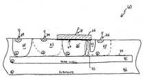
- a second isolation structure 25such as a trench 26 , is disposed at least partially in the n ⁇ well 22 , and acts to isolate second the n+ region 28 from the p+ region 18 .
- a layer of dielectric 33is disposed over a portion of the first p ⁇ well 14 , the p ⁇ well/n ⁇ well junction region 34 , a portion of n ⁇ well 22 and a portion of the first trench 24 .
- the material of dielectric 33may be the same as the material of first trench 24 , if desired.
- a gate 32is in contact with the dielectric layer 33 as well as the dielectric material in the first trench 24 .
- FIG. 2is an elevational cross-sectional diagram of a lateral diffusion p ⁇ channel MOSFET in accordance with the prior art.
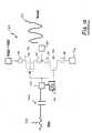
- FIG. 11is a circuit diagram showing a high-voltage digital output circuit for a lower-voltage integrated circuit device incorporating a p-channel LDMOSFET in accordance with an embodiment of the present invention.
- FIG. 4is an elevational cross-sectional diagram of elements of a LDMOSFET 76 in accordance with another embodiment of the present invention.
- This embodiment of the present inventiondiffers from that illustrated in FIG. 3 in that an additional isolation structure 77 is disposed in source well region 63 and formed of an insulating material disposed from the top of the substrate not quite to the upper surface 74 of deep well region 61 and, likewise, provides high-voltage capability by isolating the source contact 70 from the source/gate well junction 78 .
- the dimensions of various portions of the device of FIG. 7depend upon the magnitude of the voltage that is intended to power the device, and the magnitude of the voltages and currents that it will control.
- the dimension Lwis properly measured within substrate 100 .
- Dimension Lwrepresents the thickness of the portion of p-well 110 that is between isolation structure 118 and n ⁇ well 106 , and the thickness of the portion of p-well 112 that is between isolation structure 120 and n ⁇ well 106 . These dimensions are shown as equal for the left and the right of n ⁇ well 106 . This is shown as an example, but not as limitation, and the invention may be practiced with these dimensions being unequal. In general, dimension Lw needs to be wider for larger current carrying devices, and may be smaller if lesser currents are involved. Those of ordinary skill in the art will now be readily able to choose such dimensions based upon their particular application in view of the present description.
- FIG. 8a slight variation of the device of FIG. 7 is presented.
- the deviceis in all respects except one the same as that of FIG. 7 .
- the differenceis that instead of p ⁇ wells 110 and 112 the device is provided with p ⁇ substrate material at locations 110 a and 112 a .
- the advantage of this approachis that the n ⁇ well to p-substrate junction has a higher breakdown voltage due to the 2 orders of magnitude less doping of the p ⁇ substrate material as compared to the p ⁇ well material of the FIG. 7 embodiment.
- a high-voltage output analog amplifier circuit 170is shown. It comprises a high-voltage pFET (LDPMOS) 172 and a high-voltage LDNMOS 174 (similar to that of FIG. 1 ) coupled in series as shown.
- LDPMOShigh-voltage pFET
- LDNMOShigh-voltage LDNMOS
Landscapes
- Insulated Gate Type Field-Effect Transistor (AREA)
- Metal-Oxide And Bipolar Metal-Oxide Semiconductor Integrated Circuits (AREA)
Abstract
Description
- This application claims the benefit of U.S. Provisional Patent Application Ser. No. 60/565,553 filed Apr. 26, 2004 (Attorney Docket No. IMPJ-0079P) in the name of the inventor Bin Wang and commonly assigned herewith. This application is a Continuation-In-Part of U.S. patent application Ser. No. 10/884,236 filed on Jul. 2, 2004, entitled “Native High-Voltage N-Channel LDMOSFET in Standard Logic CMOS” in the name of inventor Bin Wang and commonly assigned herewith (Attorney Docket No. IMPJ-0060). This application is also a Continuation-In-Part of U.S. patent application Ser. No. 10/884,326 filed on Jul. 2, 2004, entitled “Graded-Junction High-Voltage MOSFET in Standard Logic CMOS” in the name of inventor Bin Wang and commonly assigned herewith (Attorney Docket No. IMPJ-0079).
- The present invention relates generally to high-voltage transistors, i.e., transistors designed to handle voltages in excess of their nominal power requirements (Vdd-Vss). More particularly, the present invention relates to a high-voltage LDMOSFET (laterally diffused metal oxide semiconductor field effect transistor) fabricated in a standard logic CMOS (complementary MOS) process.
- LDMOSFETs (Laterally Diffused MOSFETs) are known. Such devices are used as high-voltage switches and components in devices fabricated in various MOS process (fabrication) technologies including logic CMOS and the like, but having a need for relatively high-voltage capabilities (e.g., 10 volts in a 3.3 volt process). Such high-voltages are used in charge pumps, programming nonvolatile memory circuits, on-chip liquid crystal display drivers, on-chip field-emission display drivers, and the like. A typical LDMOSFET10 (also referred to as an LDMOS) is shown in elevational cross-section in
FIG. 1 . LDMOS10 is formed in asubstrate 12 of p-type conductivity. A first heavily doped region of n-type conductivity (“first n+ region”)13 is disposed in a first well of a p-type conductivity (“first p− well”)14 of thesubstrate 12. Asource terminal 16 is coupled to thefirst n+ region 13. A heavily doped region of p-type conductivity (“p+ region”)18 is disposed in a second well of p-type conductivity (“second p− well”)15. A p+ dopedregion 18 is disposed in second p− well15. Abody terminal 20 is coupled to p+ dopedregion 18. A well of n-type conductivity (“n− well”)22 is disposed in thesubstrate 12 between the first p−well 14 and the second p−well 15. A first isolation structure23, such as afirst trench 24, is disposed in the n− well22. The first isolation structure23 such asfirst trench 24 is filled with an insulating dielectric material such as silicon dioxide which may be deposited or grown in any convenient manner such as using the well-known Shallow Trench Isolation (STI) process (as shown) or the well-known Local Oxidation of Silicon (LOCOS) process (not shown). A second heavily doped region of the n-type conductivity (“second n+ region”)28 is disposed in the n− well22. Adrain terminal 30 is coupled to thesecond n+ region 28. Asecond isolation structure 25, such as atrench 26, is disposed at least partially in the n−well 22, and acts to isolate second then+ region 28 from thep+ region 18. A layer of dielectric33 is disposed over a portion of the first p−well 14, the p− well/n− well junction region34, a portion of n−well 22 and a portion of thefirst trench 24. In fact, the material of dielectric33 may be the same as the material offirst trench 24, if desired. Agate 32 is in contact with thedielectric layer 33 as well as the dielectric material in thefirst trench 24.Gate region 32 may comprise n+ doped polysilicon material, p+ doped polysilicon material, metal, or any other suitable material used for forming a conductive gate.Insulating sidewall spacers 36 and38 are also provided. The channel of the device extends from thesource region 13 to the first isolation structure23, as shown. The region denoted Lw is a region of lateral diffusion of the n−well 22 under the gate and Lw denotes its length. - In this device the n−
well 22 is used as the drain of the device. A high breakdown voltage is provided due to lateral diffusion in the region denoted Lw under the gate. This structure results in deep junctions with lower doping than that of a typical n+ drain. The breakdown voltage is determined by the doping concentrations in the n− well22 (approximately 1017atoms/cm3) and p− well14 (approximately 1017atoms/cm3) of the n-well/p-well junction34. The prior art embodiment shown uses shallow trench isolation (STI). Similar embodiments implementing a LOCOS isolation scheme are also well known in the art. - P-Channel high-voltage MOSFETs are also known. Turning now to
FIG. 2 , such adevice 40 is illustrated in elevational cross section. Thedevice 40 is fabricated in an n− well42 of a substrate of p-type conductivity (“p-substrate”)44. Itssource 46 is a heavily doped diffusion region of p-type conductivity, disposed in n− well42. Itsdrain 48 is a heavily doped diffusion region of p-type conductivity, formed in a lightly dopeddiffusion region 50 of p-type conductivity, which can be formed out of a “channel stop” implant using boron doping. Abody contact 52 is formed by an n+ diffusion in the n− well42. A gate54 formed of a conductive material such as heavily doped polysilicon or metal overlies a layer of dielectric55 (such as Silicon dioxide gate oxide) which, in turn, overlies a portion of thesource region 46 and the p-diffusion region 50 as shown. A pair ofisolation structures drain region 48. The p−diffusion region 50 extends frominsulating structure 58, underdrain region 48 and underinsulating structure 56. The breakdown voltage is determined by the doping concentrations in the n− well42 (approximately 1017atoms/cm3) and p− diffusion region50 (approximately 1017atoms/cm3) of the n-well/p-diffusion junction59. - As device geometries and minimum feature sizes (MFS) shrink, e.g., from 0.18 micron MFS to 0.13 micron MFS to 0.09 micron MFS and beyond, new ways to provide relatively high breakdown voltages, particularly in standard CMOS processes, become more and more important. Accordingly, it is highly desirable to provide an improved high-voltage switching device. It is also highly desirable to provide an n-channel and a p-channel high-voltage switching device, so that a high-voltage CMOS inverter and high-output-voltage analog amplifier as well as a circuit with a relatively high voltage output for a relatively low input voltage Vdd may be fabricated.
- A high-voltage LDMOSFET includes a semiconductor substrate, in which a gate well region is formed. A source well region and a drain well region are formed on either side of the gate well region, and include insulating regions within them that do not reach the full depth. An insulating layer is disposed on the substrate, covering the gate well region and a portion of the source well region and the drain well region. A conductive gate is disposed on the insulating layer. A biasing well region is formed adjacent the source well region or the drain well region or both. A deep well region is formed in the substrate such that it communicates with the biasing well region and the gate well region, while extending under the source well region and the drain well region, such as to avoid them. Biasing contacts at the top of the biasing well regions bias the deep well region, and therefore also the gate well region. In other embodiments, two biasing well regions are provided that, in combination with the deep well region, also insulate the source well region and the drain well region from the substrate.
- Trench isolation of various types, LOCOS based isolation schemes, and other suitable processes may be used for forming the isolation structures.
- Other aspects of the inventions are described and claimed below, and a further understanding of the nature and advantages of the inventions may be realized by reference to the remaining portions of the specification and the attached drawings.
- The accompanying drawings, which are incorporated into and constitute a part of this specification, illustrate one or more embodiments of the present invention and, together with the detailed description, serve to explain the principles and implementations of the invention.
- In the drawings:
FIG. 1 is an elevational cross-sectional diagram of a lateral diffusion n-channel MOSFET in accordance with the prior art.FIG. 2 is an elevational cross-sectional diagram of a lateral diffusion p− channel MOSFET in accordance with the prior art.FIG. 3 is an elevational cross-sectional diagram of elements of a LDMOSFET in accordance with one embodiment of the present invention.FIG. 4 is an elevational cross-sectional diagram of elements of a LDMOSFET in accordance with another embodiment of the present invention.FIG. 5 is an elevational cross-sectional diagram of elements of a LDMOSFET in accordance with another embodiment of the present invention.FIG. 6 is an elevational cross-sectional diagram of elements of a high-voltage LDMOSFET in accordance with yet another embodiment of the present invention.FIG. 7 is an elevational cross-sectional diagram of a high-voltage p-channel LDMOSFET in accordance with an embodiment of the present invention.FIG. 8 is an elevational cross-sectional diagram of a high-voltage p-channel LDMOSFET in accordance with another embodiment of the present invention.FIG. 9 is a circuit diagram showing a high-voltage inverter formed with a p-channel LDMOSFET in accordance with an embodiment of the present invention.FIG. 10 is a circuit diagram showing a high-output-voltage analog amplifier formed with a p-channel LDMOSFET in accordance with an embodiment of the present invention.FIG. 11 is a circuit diagram showing a high-voltage digital output circuit for a lower-voltage integrated circuit device incorporating a p-channel LDMOSFET in accordance with an embodiment of the present invention.- Embodiments of the present invention described in the following detailed description are directed at high-voltage LDMOSFET devices and applications. Those of ordinary skill in the art will realize that the detailed description is illustrative only and is not intended to restrict the scope of the claimed inventions in any way. Other embodiments of the present invention, beyond those embodiments described in the detailed description, will readily suggest themselves to those of ordinary skill in the art having the benefit of this disclosure. Reference will now be made in detail to implementations of the present invention as illustrated in the accompanying drawings. Where appropriate, the same reference indicators will be used throughout the drawings and the following detailed description to refer to the same or similar parts.
- In the interest of clarity, not all of the routine features of the implementations described herein are shown and described. It will, of course, be appreciated that in the development of any such actual implementation, numerous implementation-specific decisions must be made in order to achieve the developer's specific goals, such as compliance with application− and business-related constraints, and that these specific goals will vary from one implementation to another and from one developer to another. Moreover, it will be appreciated that such a development effort might be complex and time-consuming, but would nevertheless be a routine undertaking of engineering for those of ordinary skill in the art having the benefit of this disclosure.
- As used herein, the symbol n+ indicates an n-doped semiconductor material typically having a doping level of n-type dopants on the order of 1020atoms per cubic centimeter. The symbol n− indicates an n-doped semiconductor material typically having a doping level on the order of 1017atoms per cubic centimeter for n-doped wells and on the order of 1015atoms per cubic centimeter for n-substrate material. The symbol p+ indicates a p-doped semiconductor material typically having a doping level of p-type dopants on the order of 1020atoms per cubic centimeter. The symbol p− indicates a p-doped semiconductor material typically having a doping level on the order of 1017atoms per cubic centimeter for p− doped wells and on the order of 1015atoms per cubic centimeter for p− substrate material. Those of ordinary skill in the art will now also realize that a range of doping concentrations around those described is suitable for the present purposes. Essentially, any process capable of forming pFETs and nFETs is suitable for the present purposes. Doped regions may be diffusions or they may be implanted. When it is written that something is doped at approximately the same level as something else, the doping levels are within approximately a factor of ten of each other, e.g., 1016is within a factor of ten of 1015and 1017.
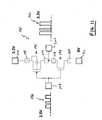
FIG. 3 is an elevational cross-sectional diagram of elements of an LDMOSFET60 in accordance with one embodiment of the present invention. In accordance with the invention ofFIG. 3 , theLDMOSFET 60 is formed in asubstrate 62 of a second conductivity type (2). Adeep well region 61 of a first conductivity type (1) is formed in thesubstrate 62, also known as deep well. If the first conductivity type is p, then the second conductivity type is n and vice versa. Asource well region 63 and adrain well region 64 of the second conductivity type are formed, which are also known as source well63 and drain well64. Agate well region 65 of the first conductivity type, also known as gate well65, is formed between the source well63 and the drain well64. Thegate well region 65 is electrically coupled to thedeep well region 61. Aconductive gate 66 is disposed over thegate well region 65 and a portion of thesource well region 63 and thedrain well region 64, and is separated from them by an insulatinglayer 67 which may be an oxide (silicon dioxide) or other suitable insulator.- A biasing well
region 68 of the first conductivity type, which is also known as biasing well68, is formed in thesubstrate 62, near either sourcewell region 63 or drain wellregion 64. The biasing well68 is electrically coupled to thedeep well region 61, so that it may be used to provide a bias signal to thedeep well region 61, and from there to thegate well region 65.Contacts biasing well region 68, thesource well region 63, theconductive gate 66 and thedrain well region 64, respectively, in a conventional manner (e.g., n+ doped diffusion region for an n− well or n− substrate region and p+ doped diffusion region for a p− well or p− substrate region).Source well region 63 and drain wellregion 64 may be wells of the second conductivity type (e.g., doped to a dopant concentration of the order of about 1017atoms of dopant per cubic centimeter, or they may be substrate material of the second conductivity type (e.g., doped to a dopant concentration of the order of about 1015atoms of dopant per cubic centimeter). Doping may be achieved by any suitable mechanism. Anisolation structure 73 disposed in thedrain well region 64 and formed of an insulating material disposed from the top of the substrate not quite to theupper surface 74 ofdeep well region 61 provides high-voltage capability by isolating thedrain contact 72 from the drain/gate well junction 75. - It will be understood that the elements shown in
FIG. 3 are intended as those of a minimum embodiment, not necessarily a full schematic. More items may be included than those shown, fordevice 60 to be a high voltage device. The embodiment ofFIG. 3 can work for purposes different than a high-voltage device, with different doping amounts than those of the preferred embodiments recommended in this document. If, however, one artificially considers the embodiment ofFIG. 3 with those elements alone, it may have problems as a high voltage device, since one or both of sourcewell region 63 and drain wellregion 64 may be shorted tosubstrate 62. The same applies also to the embodiments ofFIG. 4 andFIG. 5 . FIG. 4 is an elevational cross-sectional diagram of elements of a LDMOSFET76 in accordance with another embodiment of the present invention. This embodiment of the present invention differs from that illustrated inFIG. 3 in that an additional isolation structure77 is disposed insource well region 63 and formed of an insulating material disposed from the top of the substrate not quite to theupper surface 74 ofdeep well region 61 and, likewise, provides high-voltage capability by isolating thesource contact 70 from the source/gate well junction 78.FIG. 5 is an elevational cross-sectional diagram of elements of a LDMOSFET79 in accordance with another embodiment of the present invention. This embodiment of the present invention differs from that illustrated inFIG. 3 in that anadditional isolation structure 80 is disposed between thesource contact 70 and the biasing well contact69. Theisolation structure 80 is formed of an insulating material disposed from the top of the substrate not quite to theupper surface 74 of thedeep well region 61 and assists in isolating thesource contact 70 from thewell contact 69.FIG. 6 is an elevational cross-sectional diagram of a high-voltage LDMOSFET 81 in accordance with another embodiment of the present invention. This embodiment of the present invention differs from that illustrated inFIG. 5 in that a second biasing well84 is provided, having a secondbiasing well contact 83. The second biasing well84 is provided on the opposite side of first biasing well68, with respect to thegate region 65.- In some embodiments, an
additional isolation structure 82 is disposed between the second biasing well84 and thedrain well region 64. Theisolation structure 82 is formed of an insulating material disposed from the top of the substrate not quite to theupper surface 74 ofdeep well region 61, and assists in isolating thedrain contact 72 from the secondbiasing well contact 83. - In some embodiments, the first
biasing well region 68, together with the secondbiasing well region 84 and thedeep well region 61 are formed such that they insulate thesource well region 63 and the drain well region664 from thesubstrate 62. This is preferred for high voltage operation. - Turning now to
FIG. 7 , a p−substrate 100 is provided with a deep n− well102 through a high-energy ion implantation process well known to those of ordinary skill in the art. Over deep n− well102 are formed in an embodiment of the present invention, first, second and third n−wells wells second isolation structures wells wells fourth isolation structures 118 and120 are embedded within p−wells junctions additional isolation structures 126 and128 are formed of insulating material such as field oxide formed of silicon dioxide, silicon oxynitride, and the like. They may be formed with a LOCOS process or an STI process, for example. An insulatinglayer 129 is formed onsubstrate 100, similarly to layer67 ofFIG. 3 . Insulatinglayer 129 is on such a portion ofsubstrate 100 that covers at least portions of p−wells conductive gate 130 is disposed on insulatinglayer 129. A channel is formed under insulatinglayer 129 between p−wells gate 130. Adrain 132 and a source134 may be p+ diffusion regions disposed in respective p−wells body contacts wells 104/108 as shown. Deep n− well102 also serves to electrically couple n− well104 with n− well106 and n− well108.Insulators conductive gate 130 from other parts of the device.Conductive gate 130 may be formed from a heavily doped semiconductor material such as p+ polysilicon or a metal. - The dimensions of various portions of the device of
FIG. 7 depend upon the magnitude of the voltage that is intended to power the device, and the magnitude of the voltages and currents that it will control. The dimension Lw is properly measured withinsubstrate 100. Dimension Lw represents the thickness of the portion of p-well110 that is between isolation structure118 and n− well106, and the thickness of the portion of p-well112 that is betweenisolation structure 120 and n− well106. These dimensions are shown as equal for the left and the right of n− well106. This is shown as an example, but not as limitation, and the invention may be practiced with these dimensions being unequal. In general, dimension Lw needs to be wider for larger current carrying devices, and may be smaller if lesser currents are involved. Those of ordinary skill in the art will now be readily able to choose such dimensions based upon their particular application in view of the present description. - Turning now to
FIG. 8 , a slight variation of the device ofFIG. 7 is presented. The device is in all respects except one the same as that ofFIG. 7 . The difference is that instead of p−wells FIG. 7 embodiment. - The high-voltage devices of the invention may be used in a number of applications. Three such applications are described by way of example, but not limitation. In all three embodiments that follow, two transistors are coupled together. At least one of them, and optionally both of them, are LDMOSFET as described above. Further, they are symmetric in that where the first transistor is an LDPMOS, the second transistor is an LDNMOS.
- In
FIG. 9 a high-voltage inverter 150 is shown. It comprises a high-voltage pFET (LDPMOS)152 and a symmetrical LDNMOS154 (which may be similar to that ofFIG. 1 but with high-voltage source and drain) coupled in series as shown. Aninput signal 156 is applied to thenode 157 coupled to the gates oftransistors 152 and154, a Vdd power source of about 10V may be applied to thesource 158 ofLDPMOS 152, Vss (ground) may be applied to thesource 160 of symmetrical LDNMOS154, and theinverted signal 162 is available at thenode 164 coupled to thedrains 166 and168 oftransistors 152 and154, respectively. - In
FIG. 10 a high-voltage outputanalog amplifier circuit 170 is shown. It comprises a high-voltage pFET (LDPMOS)172 and a high-voltage LDNMOS174 (similar to that ofFIG. 1 ) coupled in series as shown. Aninput signal 175 is applied through aDC blocking capacitor 176 to the node177 coupled to the gates of transistors172 and174, asource 179 of DC bias voltage may be provided for node177, a Vdd power source of about10V may be applied to thesource 178 of LDPMOS172, Vss (ground) may be applied to the source180 of LDNMOS174 (a symmetrical LDNMOS is not required in this application), and the amplifiedsignal 182 is available at the node184 which is, in turn, coupled to thedrains 186 and188 of transistors172 and174, respectively. - The present invention may be further used in terms of providing a low cost output driver. Such can be used in a number of applications, such as for System On a Chip (SOC), and so on. An example of that is described below.
- In
FIG. 11 a high-voltage output driver 190 is shown. It comprises a high-voltage pFET (LDPMOS)192 and a high-voltage LDNMOS194 (similar to that ofFIG. 1 ) coupled in series as shown. Aninput signal 196 is applied to thenode 197 coupled to the gates of transistors192 and194. A Vdd power source of the desired output peak level may be applied to thesource 198 of LDPMOS192. A Vss (ground) may be applied to thesource 200 of LDNMOS194. It is noteworthy that the desired output peak level here is 3.3 VDC, but a different value could be used for the application. The convertedsignal 202 is available at thenode 204, coupled to thedrains - The present invention may be easily implemented in many standard MOS processes supporting deep n− wells. It makes possible to fabricate high voltage transistors, such as PMOS, in standard CMOS process.
- While embodiments and applications of this invention have been shown and described, it will now be apparent to those skilled in the art having the benefit of this disclosure that many more modifications than mentioned above are possible without departing from the inventive concepts disclosed herein. Therefore, the appended claims are intended to encompass within their scope all such modifications as are within the true spirit and scope of this invention.
Claims (42)
Priority Applications (2)
| Application Number | Priority Date | Filing Date | Title |
|---|---|---|---|
| US10/952,708US8264039B2 (en) | 2004-04-26 | 2004-09-28 | High-voltage LDMOSFET and applications therefor in standard CMOS |
| US11/138,888US7375398B2 (en) | 2004-07-02 | 2005-05-26 | High voltage FET gate structure |
Applications Claiming Priority (4)
| Application Number | Priority Date | Filing Date | Title |
|---|---|---|---|
| US56555304P | 2004-04-26 | 2004-04-26 | |
| US10/884,326US7145203B2 (en) | 2004-04-26 | 2004-07-02 | Graded-junction high-voltage MOSFET in standard logic CMOS |
| US10/884,236US7315067B2 (en) | 2004-07-02 | 2004-07-02 | Native high-voltage n-channel LDMOSFET in standard logic CMOS |
| US10/952,708US8264039B2 (en) | 2004-04-26 | 2004-09-28 | High-voltage LDMOSFET and applications therefor in standard CMOS |
Related Parent Applications (2)
| Application Number | Title | Priority Date | Filing Date |
|---|---|---|---|
| US10/884,326Continuation-In-PartUS7145203B2 (en) | 2004-04-26 | 2004-07-02 | Graded-junction high-voltage MOSFET in standard logic CMOS |
| US10/884,236Continuation-In-PartUS7315067B2 (en) | 2004-04-26 | 2004-07-02 | Native high-voltage n-channel LDMOSFET in standard logic CMOS |
Related Child Applications (2)
| Application Number | Title | Priority Date | Filing Date |
|---|---|---|---|
| US10/884,236Continuation-In-PartUS7315067B2 (en) | 2004-04-26 | 2004-07-02 | Native high-voltage n-channel LDMOSFET in standard logic CMOS |
| US11/138,888Continuation-In-PartUS7375398B2 (en) | 2004-07-02 | 2005-05-26 | High voltage FET gate structure |
Publications (2)
| Publication Number | Publication Date |
|---|---|
| US20050258461A1true US20050258461A1 (en) | 2005-11-24 |
| US8264039B2 US8264039B2 (en) | 2012-09-11 |
Family
ID=46302942
Family Applications (1)
| Application Number | Title | Priority Date | Filing Date |
|---|---|---|---|
| US10/952,708Active2028-03-28US8264039B2 (en) | 2004-04-26 | 2004-09-28 | High-voltage LDMOSFET and applications therefor in standard CMOS |
Country Status (1)
| Country | Link |
|---|---|
| US (1) | US8264039B2 (en) |
Cited By (5)
| Publication number | Priority date | Publication date | Assignee | Title |
|---|---|---|---|---|
| US20070235804A1 (en)* | 2006-04-10 | 2007-10-11 | Fuji Electric Device Technology Co., Ltd. | Soi lateral semiconductor device and method of manufacturing the same |
| US20090179272A1 (en)* | 2008-01-11 | 2009-07-16 | Campi Jr John B | Double gate depletion mode mosfet |
| CN103035647A (en)* | 2011-10-04 | 2013-04-10 | 美国博通公司 | One-time programmable device having an LDMOS structure and related method |
| CN103904082A (en)* | 2012-12-27 | 2014-07-02 | 力旺电子股份有限公司 | Nonvolatile memory structure and method for fabricating nonvolatile memory structure |
| CN104241293A (en)* | 2013-06-07 | 2014-12-24 | 力旺电子股份有限公司 | Nonvolatile memory structure |
Families Citing this family (3)
| Publication number | Priority date | Publication date | Assignee | Title |
|---|---|---|---|---|
| US8492866B1 (en) | 2012-01-09 | 2013-07-23 | International Business Machines Corporation | Isolated Zener diode |
| US9559199B2 (en) | 2014-12-18 | 2017-01-31 | Silanna Asia Pte Ltd | LDMOS with adaptively biased gate-shield |
| US11171215B2 (en) | 2014-12-18 | 2021-11-09 | Silanna Asia Pte Ltd | Threshold voltage adjustment using adaptively biased shield plate |
Citations (30)
| Publication number | Priority date | Publication date | Assignee | Title |
|---|---|---|---|---|
| US688023A (en)* | 1900-12-14 | 1901-12-03 | Daniel B Lincoln | Bottom-board for foundry-flasks. |
| US4697332A (en)* | 1984-05-25 | 1987-10-06 | Gould Inc. | Method of making tri-well CMOS by self-aligned process |
| US4745079A (en)* | 1987-03-30 | 1988-05-17 | Motorola, Inc. | Method for fabricating MOS transistors having gates with different work functions |
| US5485027A (en)* | 1988-11-08 | 1996-01-16 | Siliconix Incorporated | Isolated DMOS IC technology |
| US5553030A (en)* | 1993-09-10 | 1996-09-03 | Intel Corporation | Method and apparatus for controlling the output voltage provided by a charge pump circuit |
| US5585660A (en)* | 1994-04-08 | 1996-12-17 | Texas Instruments Incorporated | Extended drain resurf lateral DMOS devices |
| US5593909A (en)* | 1993-06-25 | 1997-01-14 | Samsung Electronics Co., Ltd. | Method for fabricating a MOS transistor having an offset resistance |
| US5751042A (en)* | 1996-02-15 | 1998-05-12 | Winbond Electronics Corporation | Internal ESD protection circuit for semiconductor devices |
| US5753952A (en)* | 1995-09-22 | 1998-05-19 | Texas Instruments Incorporated | Nonvolatile memory cell with P-N junction formed in polysilicon floating gate |
| US6023188A (en)* | 1996-11-05 | 2000-02-08 | Aplus Flash Technology, Inc. | Positive/negative high voltage charge pump system |
| US6097070A (en)* | 1999-02-16 | 2000-08-01 | International Business Machines Corporation | MOSFET structure and process for low gate induced drain leakage (GILD) |
| US6160289A (en)* | 1995-10-13 | 2000-12-12 | Hyundai Electronics Industries Co., Ltd. | RESURF EDMOS transistor and high-voltage analog multiplexer circuit using the same |
| US6160290A (en)* | 1997-11-25 | 2000-12-12 | Texas Instruments Incorporated | Reduced surface field device having an extended field plate and method for forming the same |
| US6177830B1 (en)* | 1999-03-05 | 2001-01-23 | Xilinx, Inc | High voltage charge pump using standard sub 0.35 micron CMOS process |
| US6211552B1 (en)* | 1999-05-27 | 2001-04-03 | Texas Instruments Incorporated | Resurf LDMOS device with deep drain region |
| US6350637B1 (en)* | 1999-04-06 | 2002-02-26 | Stmicroelectronics S.R.L. | Method of fabrication of a no-field MOS transistor |
| US20020028541A1 (en)* | 2000-08-14 | 2002-03-07 | Lee Thomas H. | Dense arrays and charge storage devices, and methods for making same |
| US6461918B1 (en)* | 1999-12-20 | 2002-10-08 | Fairchild Semiconductor Corporation | Power MOS device with improved gate charge performance |
| US6548874B1 (en)* | 1999-10-27 | 2003-04-15 | Texas Instruments Incorporated | Higher voltage transistors for sub micron CMOS processes |
| US6555883B1 (en)* | 2001-10-29 | 2003-04-29 | Power Integrations, Inc. | Lateral power MOSFET for high switching speeds |
| US6593621B2 (en)* | 2001-08-23 | 2003-07-15 | Micrel, Inc. | LDMOS field effect transistor with improved ruggedness in narrow curved areas |
| US6661278B1 (en)* | 2002-07-08 | 2003-12-09 | Impinj, Inc. | High voltage charge pump circuit |
| US6665012B1 (en)* | 1998-09-22 | 2003-12-16 | Pixim, Inc. | Process-scalable high spatial resolution and low bit resolution CMOS area image sensor |
| US6678190B2 (en)* | 2002-01-25 | 2004-01-13 | Ememory Technology Inc. | Single poly embedded eprom |
| US6730458B1 (en)* | 2003-03-03 | 2004-05-04 | Samsung Electronics Co., Ltd. | Method for forming fine patterns through effective glass transition temperature reduction |
| US6734493B2 (en)* | 2002-02-08 | 2004-05-11 | Taiwan Semiconductor Manufacturing Co., Ltd. | Lateral double diffused metal oxide semiconductor (LDMOS) device with aligned buried layer isolation layer |
| US6831331B2 (en)* | 1995-11-15 | 2004-12-14 | Denso Corporation | Power MOS transistor for absorbing surge current |
| US6873021B1 (en)* | 2003-12-02 | 2005-03-29 | Texas Instruments Incorporated | MOS transistors having higher drain current without reduced breakdown voltage |
| US6989302B2 (en)* | 2003-05-05 | 2006-01-24 | Texas Instruments Incorporated | Method for fabricating a p-type shallow junction using diatomic arsenic |
| US7091535B2 (en)* | 2004-03-05 | 2006-08-15 | Taiwan Semiconductor Manufacturing Company | High voltage device embedded non-volatile memory cell and fabrication method |
Family Cites Families (2)
| Publication number | Priority date | Publication date | Assignee | Title |
|---|---|---|---|---|
| US6965142B2 (en) | 1995-03-07 | 2005-11-15 | Impinj, Inc. | Floating-gate semiconductor structures |
| US6882023B2 (en) | 2002-10-31 | 2005-04-19 | Motorola, Inc. | Floating resurf LDMOSFET and method of manufacturing same |
- 2004
- 2004-09-28USUS10/952,708patent/US8264039B2/enactiveActive
Patent Citations (31)
| Publication number | Priority date | Publication date | Assignee | Title |
|---|---|---|---|---|
| US688023A (en)* | 1900-12-14 | 1901-12-03 | Daniel B Lincoln | Bottom-board for foundry-flasks. |
| US4697332A (en)* | 1984-05-25 | 1987-10-06 | Gould Inc. | Method of making tri-well CMOS by self-aligned process |
| US4745079A (en)* | 1987-03-30 | 1988-05-17 | Motorola, Inc. | Method for fabricating MOS transistors having gates with different work functions |
| US5485027A (en)* | 1988-11-08 | 1996-01-16 | Siliconix Incorporated | Isolated DMOS IC technology |
| US5593909A (en)* | 1993-06-25 | 1997-01-14 | Samsung Electronics Co., Ltd. | Method for fabricating a MOS transistor having an offset resistance |
| US5553030A (en)* | 1993-09-10 | 1996-09-03 | Intel Corporation | Method and apparatus for controlling the output voltage provided by a charge pump circuit |
| US5585660A (en)* | 1994-04-08 | 1996-12-17 | Texas Instruments Incorporated | Extended drain resurf lateral DMOS devices |
| US5753952A (en)* | 1995-09-22 | 1998-05-19 | Texas Instruments Incorporated | Nonvolatile memory cell with P-N junction formed in polysilicon floating gate |
| US6559683B1 (en)* | 1995-10-13 | 2003-05-06 | Hyundai Electronics Industries, Co., Ltd. | Resurf EDMOS transistor and high-voltage analog multiplexer circuit using the same |
| US6160289A (en)* | 1995-10-13 | 2000-12-12 | Hyundai Electronics Industries Co., Ltd. | RESURF EDMOS transistor and high-voltage analog multiplexer circuit using the same |
| US6831331B2 (en)* | 1995-11-15 | 2004-12-14 | Denso Corporation | Power MOS transistor for absorbing surge current |
| US5751042A (en)* | 1996-02-15 | 1998-05-12 | Winbond Electronics Corporation | Internal ESD protection circuit for semiconductor devices |
| US6023188A (en)* | 1996-11-05 | 2000-02-08 | Aplus Flash Technology, Inc. | Positive/negative high voltage charge pump system |
| US6160290A (en)* | 1997-11-25 | 2000-12-12 | Texas Instruments Incorporated | Reduced surface field device having an extended field plate and method for forming the same |
| US6665012B1 (en)* | 1998-09-22 | 2003-12-16 | Pixim, Inc. | Process-scalable high spatial resolution and low bit resolution CMOS area image sensor |
| US6097070A (en)* | 1999-02-16 | 2000-08-01 | International Business Machines Corporation | MOSFET structure and process for low gate induced drain leakage (GILD) |
| US6177830B1 (en)* | 1999-03-05 | 2001-01-23 | Xilinx, Inc | High voltage charge pump using standard sub 0.35 micron CMOS process |
| US6350637B1 (en)* | 1999-04-06 | 2002-02-26 | Stmicroelectronics S.R.L. | Method of fabrication of a no-field MOS transistor |
| US6211552B1 (en)* | 1999-05-27 | 2001-04-03 | Texas Instruments Incorporated | Resurf LDMOS device with deep drain region |
| US6548874B1 (en)* | 1999-10-27 | 2003-04-15 | Texas Instruments Incorporated | Higher voltage transistors for sub micron CMOS processes |
| US6461918B1 (en)* | 1999-12-20 | 2002-10-08 | Fairchild Semiconductor Corporation | Power MOS device with improved gate charge performance |
| US20020028541A1 (en)* | 2000-08-14 | 2002-03-07 | Lee Thomas H. | Dense arrays and charge storage devices, and methods for making same |
| US6593621B2 (en)* | 2001-08-23 | 2003-07-15 | Micrel, Inc. | LDMOS field effect transistor with improved ruggedness in narrow curved areas |
| US6555883B1 (en)* | 2001-10-29 | 2003-04-29 | Power Integrations, Inc. | Lateral power MOSFET for high switching speeds |
| US6678190B2 (en)* | 2002-01-25 | 2004-01-13 | Ememory Technology Inc. | Single poly embedded eprom |
| US6734493B2 (en)* | 2002-02-08 | 2004-05-11 | Taiwan Semiconductor Manufacturing Co., Ltd. | Lateral double diffused metal oxide semiconductor (LDMOS) device with aligned buried layer isolation layer |
| US6661278B1 (en)* | 2002-07-08 | 2003-12-09 | Impinj, Inc. | High voltage charge pump circuit |
| US6730458B1 (en)* | 2003-03-03 | 2004-05-04 | Samsung Electronics Co., Ltd. | Method for forming fine patterns through effective glass transition temperature reduction |
| US6989302B2 (en)* | 2003-05-05 | 2006-01-24 | Texas Instruments Incorporated | Method for fabricating a p-type shallow junction using diatomic arsenic |
| US6873021B1 (en)* | 2003-12-02 | 2005-03-29 | Texas Instruments Incorporated | MOS transistors having higher drain current without reduced breakdown voltage |
| US7091535B2 (en)* | 2004-03-05 | 2006-08-15 | Taiwan Semiconductor Manufacturing Company | High voltage device embedded non-volatile memory cell and fabrication method |
Cited By (18)
| Publication number | Priority date | Publication date | Assignee | Title |
|---|---|---|---|---|
| US20070235804A1 (en)* | 2006-04-10 | 2007-10-11 | Fuji Electric Device Technology Co., Ltd. | Soi lateral semiconductor device and method of manufacturing the same |
| US7476942B2 (en)* | 2006-04-10 | 2009-01-13 | Fuji Electric Device Technology Co., Ltd. | SOI lateral semiconductor device and method of manufacturing the same |
| US20090179272A1 (en)* | 2008-01-11 | 2009-07-16 | Campi Jr John B | Double gate depletion mode mosfet |
| US7902606B2 (en)* | 2008-01-11 | 2011-03-08 | International Business Machines Corporation | Double gate depletion mode MOSFET |
| US20110117711A1 (en)* | 2008-01-11 | 2011-05-19 | International Business Machines Corporation | Double gate depletion mode mosfet |
| US8168500B2 (en) | 2008-01-11 | 2012-05-01 | International Business Machines Corporation | Double gate depletion mode MOSFET |
| EP2579310A3 (en)* | 2011-10-04 | 2013-09-04 | Broadcom Corporation | One-time programmable device having an LDMOS structure and related manufacturing method |
| US8493767B2 (en)* | 2011-10-04 | 2013-07-23 | Broadcom Corporation | One-time programmable device having an LDMOS structure |
| CN103035647A (en)* | 2011-10-04 | 2013-04-10 | 美国博通公司 | One-time programmable device having an LDMOS structure and related method |
| US20130302960A1 (en)* | 2011-10-04 | 2013-11-14 | Broadcom Corporation | One-Time Programmable Device |
| US8932912B2 (en)* | 2011-10-04 | 2015-01-13 | Broadcom Corporation | One-time programmable device |
| US8969957B2 (en) | 2011-10-04 | 2015-03-03 | Broadcom Corporation | LDMOS one-time programmable device |
| TWI499007B (en)* | 2011-10-04 | 2015-09-01 | Broadcom Corp | One-time programmable device with laterally diffused metal oxide semiconductor structure and method of fabricating the same |
| CN103904082A (en)* | 2012-12-27 | 2014-07-02 | 力旺电子股份有限公司 | Nonvolatile memory structure and method for fabricating nonvolatile memory structure |
| US20140183612A1 (en)* | 2012-12-27 | 2014-07-03 | Ememory Technology Inc. | Nonvolatile memory structure and fabrication method thereof |
| US20140242763A1 (en)* | 2012-12-27 | 2014-08-28 | Ememory Technology Inc. | Method for fabricating nonvolatile memory structure |
| US9018691B2 (en)* | 2012-12-27 | 2015-04-28 | Ememory Technology Inc. | Nonvolatile memory structure and fabrication method thereof |
| CN104241293A (en)* | 2013-06-07 | 2014-12-24 | 力旺电子股份有限公司 | Nonvolatile memory structure |
Also Published As
| Publication number | Publication date |
|---|---|
| US8264039B2 (en) | 2012-09-11 |
Similar Documents
| Publication | Publication Date | Title |
|---|---|---|
| US7145203B2 (en) | Graded-junction high-voltage MOSFET in standard logic CMOS | |
| US7315067B2 (en) | Native high-voltage n-channel LDMOSFET in standard logic CMOS | |
| US6828638B2 (en) | Decoupling capacitors for thin gate oxides | |
| US6504209B2 (en) | High-voltage transistor with buried conduction layer | |
| US9748383B2 (en) | Transistor | |
| US7671423B2 (en) | Resistor ballasted transistors | |
| US20040070050A1 (en) | Structures of vertical resistors and FETs as controlled by electrical field penetration and a band-gap voltage reference using vertical FETs operating in accumulation through the field penetration effect | |
| US7344947B2 (en) | Methods of performance improvement of HVMOS devices | |
| TWI637463B (en) | High voltage transistor device | |
| US20200006489A1 (en) | MOSFET Having Drain Region Formed Between Two Gate Electrodes with Body Contact Region and Source Region Formed in a Double Well Region | |
| US6674127B2 (en) | Semiconductor integrated circuit | |
| US7804155B2 (en) | Vertical resistors | |
| US20060284265A1 (en) | High voltage N-channel LDMOS devices built in a deep submicron CMOS process | |
| JP4166010B2 (en) | Horizontal high voltage MOSFET and semiconductor device having the same | |
| CN111799330B (en) | LDMOS with diode-coupled isolation ring | |
| US8264039B2 (en) | High-voltage LDMOSFET and applications therefor in standard CMOS | |
| US5072267A (en) | Complementary field effect transistor | |
| US20030178683A1 (en) | Semiconductor device | |
| US8022506B2 (en) | SOI device with more immunity from substrate voltage | |
| US7345347B2 (en) | Semiconductor device | |
| JP2024059850A (en) | Semiconductor device and semiconductor device manufacturing method | |
| JP2013041891A (en) | Semiconductor device | |
| US20220140105A1 (en) | Fet using trench isolation as the gate dielectric | |
| US20230246068A1 (en) | Field effect transistor having a dielectric structure | |
| US20240145580A1 (en) | Field-effect transistor with a dielectric structure having a gate dielectric and a shielding dielectric |
Legal Events
| Date | Code | Title | Description |
|---|---|---|---|
| AS | Assignment | Owner name:IMPINJI, INC., WASHINGTON Free format text:ASSIGNMENT OF ASSIGNORS INTEREST;ASSIGNORS:WANG, BIN;COLLERAN, WILLIAM T.;WANG, CHIH-HSIN;REEL/FRAME:015606/0346;SIGNING DATES FROM 20041230 TO 20050112 Owner name:IMPINJI, INC., WASHINGTON Free format text:ASSIGNMENT OF ASSIGNORS INTEREST;ASSIGNORS:WANG, BIN;COLLERAN, WILLIAM T.;WANG, CHIH-HSIN;SIGNING DATES FROM 20041230 TO 20050112;REEL/FRAME:015606/0346 | |
| AS | Assignment | Owner name:IMPINJ, INC., WASHINGTON Free format text:ASSIGNMENT OF ASSIGNORS INTEREST;ASSIGNORS:WANG, BIN;COLLERAN, WILLIAM T.;WANG, CHIH-HSIN;REEL/FRAME:015773/0615;SIGNING DATES FROM 20041230 TO 20050112 Owner name:IMPINJ, INC., WASHINGTON Free format text:ASSIGNMENT OF ASSIGNORS INTEREST;ASSIGNORS:WANG, BIN;COLLERAN, WILLIAM T.;WANG, CHIH-HSIN;SIGNING DATES FROM 20041230 TO 20050112;REEL/FRAME:015773/0615 | |
| AS | Assignment | Owner name:VIRAGE LOGIC CORPORATION, CALIFORNIA Free format text:ASSIGNMENT OF ASSIGNORS INTEREST;ASSIGNOR:IMPINJ, INC.;REEL/FRAME:021637/0351 Effective date:20080625 Owner name:VIRAGE LOGIC CORPORATION,CALIFORNIA Free format text:ASSIGNMENT OF ASSIGNORS INTEREST;ASSIGNOR:IMPINJ, INC.;REEL/FRAME:021637/0351 Effective date:20080625 | |
| AS | Assignment | Owner name:SYNOPSYS, INC., CALIFORNIA Free format text:ASSIGNMENT OF ASSIGNORS INTEREST;ASSIGNORS:VIRAGE LOGIC CORPORATION;VL C.V.;ARC CORES LIMITED;AND OTHERS;REEL/FRAME:025105/0907 Effective date:20100902 | |
| STCF | Information on status: patent grant | Free format text:PATENTED CASE | |
| FPAY | Fee payment | Year of fee payment:4 | |
| MAFP | Maintenance fee payment | Free format text:PAYMENT OF MAINTENANCE FEE, 8TH YEAR, LARGE ENTITY (ORIGINAL EVENT CODE: M1552); ENTITY STATUS OF PATENT OWNER: LARGE ENTITY Year of fee payment:8 | |
| MAFP | Maintenance fee payment | Free format text:PAYMENT OF MAINTENANCE FEE, 12TH YEAR, LARGE ENTITY (ORIGINAL EVENT CODE: M1553); ENTITY STATUS OF PATENT OWNER: LARGE ENTITY Year of fee payment:12 |