US20050258451A1 - Methods of fabricating nitride-based transistors having regrown ohmic contact regions and nitride-based transistors having regrown ohmic contact regions - Google Patents
Methods of fabricating nitride-based transistors having regrown ohmic contact regions and nitride-based transistors having regrown ohmic contact regionsDownload PDFInfo
- Publication number
- US20050258451A1 US20050258451A1US10/849,617US84961704AUS2005258451A1US 20050258451 A1US20050258451 A1US 20050258451A1US 84961704 AUS84961704 AUS 84961704AUS 2005258451 A1US2005258451 A1US 2005258451A1
- Authority
- US
- United States
- Prior art keywords
- contact
- layer
- forming
- nitride
- channel layer
- Prior art date
- Legal status (The legal status is an assumption and is not a legal conclusion. Google has not performed a legal analysis and makes no representation as to the accuracy of the status listed.)
- Granted
Links
- 150000004767nitridesChemical class0.000titleclaimsabstractdescription145
- 238000000034methodMethods0.000titleclaimsabstractdescription84
- 230000004888barrier functionEffects0.000claimsabstractdescription117
- 239000000463materialSubstances0.000claimsabstractdescription85
- 239000004065semiconductorSubstances0.000claimsabstractdescription60
- 239000000758substrateSubstances0.000claimsabstractdescription29
- 238000004519manufacturing processMethods0.000claimsabstractdescription23
- 238000005137deposition processMethods0.000claimsabstractdescription10
- 229910002704AlGaNInorganic materials0.000claimsdescription33
- 230000000873masking effectEffects0.000claimsdescription32
- 229910052751metalInorganic materials0.000claimsdescription30
- 239000002184metalSubstances0.000claimsdescription30
- 230000015572biosynthetic processEffects0.000claimsdescription19
- 229910052581Si3N4Inorganic materials0.000claimsdescription18
- HQVNEWCFYHHQES-UHFFFAOYSA-Nsilicon nitrideChemical compoundN12[Si]34N5[Si]62N3[Si]51N64HQVNEWCFYHHQES-UHFFFAOYSA-N0.000claimsdescription18
- 238000000059patterningMethods0.000claimsdescription15
- 238000002248hydride vapour-phase epitaxyMethods0.000claimsdescription13
- 229910052710siliconInorganic materials0.000claimsdescription12
- 238000000137annealingMethods0.000claimsdescription11
- 238000005229chemical vapour depositionMethods0.000claimsdescription11
- 238000004544sputter depositionMethods0.000claimsdescription8
- 238000001451molecular beam epitaxyMethods0.000claimsdescription7
- 238000002161passivationMethods0.000claimsdescription7
- 230000008569processEffects0.000claimsdescription6
- VYPSYNLAJGMNEJ-UHFFFAOYSA-NSilicium dioxideChemical compoundO=[Si]=OVYPSYNLAJGMNEJ-UHFFFAOYSA-N0.000claimsdescription5
- 230000005533two-dimensional electron gasEffects0.000claimsdescription5
- 229910001092metal group alloyInorganic materials0.000claimsdescription4
- 229910052814silicon oxideInorganic materials0.000claimsdescription3
- 229920002120photoresistant polymerPolymers0.000claimsdescription2
- 229910002601GaNInorganic materials0.000description31
- HBMJWWWQQXIZIP-UHFFFAOYSA-Nsilicon carbideChemical compound[Si+]#[C-]HBMJWWWQQXIZIP-UHFFFAOYSA-N0.000description14
- 238000000151depositionMethods0.000description13
- 230000008021depositionEffects0.000description13
- 229910010271silicon carbideInorganic materials0.000description13
- IJGRMHOSHXDMSA-UHFFFAOYSA-NAtomic nitrogenChemical compoundN#NIJGRMHOSHXDMSA-UHFFFAOYSA-N0.000description6
- JMASRVWKEDWRBT-UHFFFAOYSA-NGallium nitrideChemical compound[Ga]#NJMASRVWKEDWRBT-UHFFFAOYSA-N0.000description6
- JBRZTFJDHDCESZ-UHFFFAOYSA-NAsGaChemical compound[As]#[Ga]JBRZTFJDHDCESZ-UHFFFAOYSA-N0.000description5
- RNQKDQAVIXDKAG-UHFFFAOYSA-Naluminum galliumChemical compound[Al].[Ga]RNQKDQAVIXDKAG-UHFFFAOYSA-N0.000description5
- 238000001020plasma etchingMethods0.000description5
- 230000007704transitionEffects0.000description5
- 229910001218Gallium arsenideInorganic materials0.000description4
- XUIMIQQOPSSXEZ-UHFFFAOYSA-NSiliconChemical compound[Si]XUIMIQQOPSSXEZ-UHFFFAOYSA-N0.000description4
- 229910052782aluminiumInorganic materials0.000description4
- XAGFODPZIPBFFR-UHFFFAOYSA-NaluminiumChemical compound[Al]XAGFODPZIPBFFR-UHFFFAOYSA-N0.000description4
- 150000001875compoundsChemical class0.000description4
- 238000005530etchingMethods0.000description4
- 239000010703siliconSubstances0.000description4
- 230000015556catabolic processEffects0.000description3
- 239000013078crystalSubstances0.000description3
- 239000002019doping agentSubstances0.000description3
- 238000002513implantationMethods0.000description3
- 229910052757nitrogenInorganic materials0.000description3
- 230000006911nucleationEffects0.000description3
- 238000010899nucleationMethods0.000description3
- 229910052594sapphireInorganic materials0.000description3
- 239000010980sapphireSubstances0.000description3
- 229910020776SixNyInorganic materials0.000description2
- 230000008901benefitEffects0.000description2
- PMHQVHHXPFUNSP-UHFFFAOYSA-Mcopper(1+);methylsulfanylmethane;bromideChemical compoundBr[Cu].CSCPMHQVHHXPFUNSP-UHFFFAOYSA-M0.000description2
- 239000003989dielectric materialSubstances0.000description2
- 230000005669field effectEffects0.000description2
- 239000007943implantSubstances0.000description2
- 238000005468ion implantationMethods0.000description2
- 230000001788irregularEffects0.000description2
- 238000004518low pressure chemical vapour depositionMethods0.000description2
- 238000000623plasma-assisted chemical vapour depositionMethods0.000description2
- -1AlInGaNInorganic materials0.000description1
- GYHNNYVSQQEPJS-UHFFFAOYSA-NGalliumChemical compound[Ga]GYHNNYVSQQEPJS-UHFFFAOYSA-N0.000description1
- 238000009825accumulationMethods0.000description1
- 239000000969carrierSubstances0.000description1
- 230000008859changeEffects0.000description1
- 238000005336crackingMethods0.000description1
- 230000007547defectEffects0.000description1
- 230000005684electric fieldEffects0.000description1
- 229910052733galliumInorganic materials0.000description1
- 239000012535impuritySubstances0.000description1
- 229910052738indiumInorganic materials0.000description1
- APFVFJFRJDLVQX-UHFFFAOYSA-Nindium atomChemical compound[In]APFVFJFRJDLVQX-UHFFFAOYSA-N0.000description1
- 150000002500ionsChemical class0.000description1
- 238000002955isolationMethods0.000description1
- 239000000203mixtureSubstances0.000description1
- 229910052759nickelInorganic materials0.000description1
- TWNQGVIAIRXVLR-UHFFFAOYSA-Noxo(oxoalumanyloxy)alumaneChemical compoundO=[Al]O[Al]=OTWNQGVIAIRXVLR-UHFFFAOYSA-N0.000description1
- 229910052763palladiumInorganic materials0.000description1
- 230000003071parasitic effectEffects0.000description1
- 230000000737periodic effectEffects0.000description1
- 229910052697platinumInorganic materials0.000description1
- 230000010287polarizationEffects0.000description1
- 238000004886process controlMethods0.000description1
- 230000008439repair processEffects0.000description1
- 229920006395saturated elastomerPolymers0.000description1
- 229910021332silicideInorganic materials0.000description1
- FVBUAEGBCNSCDD-UHFFFAOYSA-Nsilicide(4-)Chemical compound[Si-4]FVBUAEGBCNSCDD-UHFFFAOYSA-N0.000description1
- 235000012239silicon dioxideNutrition0.000description1
- 239000000377silicon dioxideSubstances0.000description1
Images


Classifications
- H—ELECTRICITY
- H10—SEMICONDUCTOR DEVICES; ELECTRIC SOLID-STATE DEVICES NOT OTHERWISE PROVIDED FOR
- H10D—INORGANIC ELECTRIC SEMICONDUCTOR DEVICES
- H10D30/00—Field-effect transistors [FET]
- H—ELECTRICITY
- H10—SEMICONDUCTOR DEVICES; ELECTRIC SOLID-STATE DEVICES NOT OTHERWISE PROVIDED FOR
- H10D—INORGANIC ELECTRIC SEMICONDUCTOR DEVICES
- H10D30/00—Field-effect transistors [FET]
- H10D30/40—FETs having zero-dimensional [0D], one-dimensional [1D] or two-dimensional [2D] charge carrier gas channels
- H10D30/47—FETs having zero-dimensional [0D], one-dimensional [1D] or two-dimensional [2D] charge carrier gas channels having 2D charge carrier gas channels, e.g. nanoribbon FETs or high electron mobility transistors [HEMT]
- H10D30/471—High electron mobility transistors [HEMT] or high hole mobility transistors [HHMT]
- H10D30/475—High electron mobility transistors [HEMT] or high hole mobility transistors [HHMT] having wider bandgap layer formed on top of lower bandgap active layer, e.g. undoped barrier HEMTs such as i-AlGaN/GaN HEMTs
- H10D30/4755—High electron mobility transistors [HEMT] or high hole mobility transistors [HHMT] having wider bandgap layer formed on top of lower bandgap active layer, e.g. undoped barrier HEMTs such as i-AlGaN/GaN HEMTs having wide bandgap charge-carrier supplying layers, e.g. modulation doped HEMTs such as n-AlGaAs/GaAs HEMTs
- H—ELECTRICITY
- H10—SEMICONDUCTOR DEVICES; ELECTRIC SOLID-STATE DEVICES NOT OTHERWISE PROVIDED FOR
- H10D—INORGANIC ELECTRIC SEMICONDUCTOR DEVICES
- H10D30/00—Field-effect transistors [FET]
- H10D30/01—Manufacture or treatment
- H10D30/012—Manufacture or treatment of static induction transistors [SIT], e.g. permeable base transistors [PBT]
- H—ELECTRICITY
- H10—SEMICONDUCTOR DEVICES; ELECTRIC SOLID-STATE DEVICES NOT OTHERWISE PROVIDED FOR
- H10D—INORGANIC ELECTRIC SEMICONDUCTOR DEVICES
- H10D30/00—Field-effect transistors [FET]
- H10D30/40—FETs having zero-dimensional [0D], one-dimensional [1D] or two-dimensional [2D] charge carrier gas channels
- H10D30/47—FETs having zero-dimensional [0D], one-dimensional [1D] or two-dimensional [2D] charge carrier gas channels having 2D charge carrier gas channels, e.g. nanoribbon FETs or high electron mobility transistors [HEMT]
- H—ELECTRICITY
- H10—SEMICONDUCTOR DEVICES; ELECTRIC SOLID-STATE DEVICES NOT OTHERWISE PROVIDED FOR
- H10D—INORGANIC ELECTRIC SEMICONDUCTOR DEVICES
- H10D62/00—Semiconductor bodies, or regions thereof, of devices having potential barriers
- H10D62/80—Semiconductor bodies, or regions thereof, of devices having potential barriers characterised by the materials
- H10D62/85—Semiconductor bodies, or regions thereof, of devices having potential barriers characterised by the materials being Group III-V materials, e.g. GaAs
- H10D62/8503—Nitride Group III-V materials, e.g. AlN or GaN
Definitions
- the present inventionrelates to semiconductor devices and, more particularly, to transistors that incorporate nitride-based active layers.
- the present inventionrelates to transistors formed of semiconductor materials that can make them suitable for high power, high temperature, and/or high frequency applications.
- Materialssuch as silicon (Si) and gallium arsenide (GaAs) have found wide application in semiconductor devices for lower power and (in the case of Si) lower frequency applications.
- Sisilicon
- GaAsgallium arsenide
- These, more familiar, semiconductor materialsmay not be well suited for higher power and/or high frequency applications, however, because of their relatively small bandgaps (e.g., 1.12 eV for Si and 1.42 for GaAs at room temperature) and/or relatively small breakdown voltages.
- HEMTHigh Electron Mobility Transistor
- MODFETmodulation doped field effect transistor
- This combination of high carrier concentration and high carrier mobilitycan give the HEMT a very large transconductance and may provide a strong performance advantage over metal-semiconductor field effect transistors (MESFETs) for high-frequency applications.
- MESFETsmetal-semiconductor field effect transistors
- High electron mobility transistors fabricated in the gallium nitride/aluminum gallium nitride (GaN/AlGaN) material systemhave the potential to generate large amounts of RF power because of the combination of material characteristics that includes the aforementioned high breakdown fields, their wide bandgaps, large conduction band offset, and/or high saturated electron drift velocity.
- a major portion of the electrons in the 2DEGis attributed to polarization in the AlGaN.
- HEMTs in the GaN/AlGaN systemhave already been demonstrated.
- U.S. Pat. Nos. 5,192,987 and 5,296,395describe AlGaN/GaN HEMT structures and methods of manufacture.
- ohmic contactsfor such transistors.
- ohmic contactshave been formed through reactive ion etching (RIE) recesses for the contacts.
- RIEreactive ion etching
- Ohmic contacts that are formed without RIEhave, typically, used high annealing temperatures (e.g. 900° C.). Such high annealing temperatures may damage the materials and/or the device.
- Some embodiments of the present inventionprovide for fabrication of a transistor including forming a nitride-based channel layer on a substrate, forming a barrier layer on the nitride-based channel layer, forming a contact recess in the barrier layer to expose a contact region of the nitride-based channel layer and forming a contact layer on the exposed contact region of the nitride-based channel layer using a low temperature deposition process. Fabrication may also include forming an ohmic contact on the contact layer and forming a gate contact disposed on the barrier layer adjacent the ohmic contact.
- forming a contact layer on the exposed contact region of the nitride-based channel layer using a low temperature deposition processincludes forming a contact layer by metal organic chemical vapor deposition (MOCVD), molecular beam epitaxy (MBE), plasma enchanced chemical vapor deposition (PECVD), sputtering and/or hydride vapor phase epitaxy (HVPE).
- MOCVDmetal organic chemical vapor deposition
- MBEmolecular beam epitaxy
- PECVDplasma enchanced chemical vapor deposition
- HVPEhydride vapor phase epitaxy
- the low temperature deposition processmay be a process other than mass transport from a wafer on which the transistor is formed.
- fabrication of the transistorfurther includes forming a first dielectric layer on the barrier layer and forming a recess in the first dielectric layer.
- Forming a gate contactincludes forming a gate contact in the recess.
- Forming a contact recessincludes forming a contact recess in the first dielectric layer and the barrier layer that exposes a portion of the nitride-based channel layer.
- the gate contactmay be formed on the first dielectric layer.
- the first dielectric layercomprises a silicon nitride layer.
- the silicon nitride layermay provide a passivation layer for the transistor.
- the contact recessextends into the channel layer.
- forming an ohmic contactmay include forming an ohmic contact without annealing the ohmic contact. Forming an ohmic contact could include patterning a metal layer on the contact layer and annealing the patterned metal layer at a temperature of about 850° C. or less.
- forming a contact layer on the exposed portions of the nitride-based channel layerincludes forming a contact layer on the exposed portion of the nitride-based channel layer to a thickness sufficient to provide a sheet resistivity of less than a sheet resistivity of a two-dimensional electron gas region formed at an interface between the channel layer and the barrier layer.
- Forming a contact layermay include forming n-type an InGaN, AlInN, AlInGaN and/or InN layer.
- the n-type nitride-based layer formedis GaN and/or AlGaN.
- the InGaN, GaN, AlGaN, AlInN, AlInGaN and/or InN layermay be doped with Si, Ge and/or O during formation.
- the contact layerincludes an n-type degenerate semiconductor material other than GaN and AlGaN.
- the contact layermay include a non-nitride Group III-V semiconductor material, a Group IV semiconductor material and/or a group III-VI semiconductor material.
- fabrication of the transistorfurther includes forming sidewalls of the channel layer to provide an increased surface area interface between the channel layer and the n-type contact layer as compared to a planar interface.
- Forming an ohmic contact on the contact layermay include forming an ohmic contact on the contact layer that extends onto a portion of the channel layer or that terminates before the sidewall of the channel layer.
- fabrication of the transistorincludes forming holes in the channel layer adjacent the contact regions and placing n-type nitride-based semiconductor material in the holes. Forming an ohmic contact on the contact layer further includes forming an ohmic contact on the contact layer and on the nitride-based semiconductor material in the holes.
- the contact layerextends onto the barrier layer.
- fabricating a transistorincludes forming a nitride-based channel layer on a substrate, forming a barrier layer on the nitride-based channel layer, forming a masking layer on the barrier layer, patterning the masking layer and the barrier layer to provide contact opening that exposes a portion of the nitride-based channel layer, forming a contact layer on the exposed portion of the nitride-based channel layer and the masking layer, selectively removing the masking layer and a portion of the contact layer on the masking layer to provide a contact region, forming an ohmic contact on the contact region and forming a gate contact disposed on the barrier layer adjacent the ohmic contact.
- Fabrication of the transistormay also include forming a first dielectric layer on the barrier layer and forming a recess in the first dielectric layer.
- Forming a gate contactmay include forming a gate contact in the recess.
- Forming a masking layer on the barrier layermay include forming a masking layer on the first dielectric layer.
- Patterning the masking layer and the barrier layer to provide contact openings that expose a portion of the nitride-based channel layermay include patterning the masking layer, the first dielectric layer and the barrier layer to provide contact opening that exposes a portion of the nitride-based channel layer.
- the first dielectric layerincludes a silicon nitride layer.
- the silicon nitride layermay provide a passivation layer for the transistor.
- the masking layermay be a dielectric layer.
- the dielectric layermay be a silicon oxide layer.
- the masking layercould be a photoresist masking layer.
- Forming an ohmic contactmay be provided by forming an ohmic contact without annealing the ohmic contact.
- forming an ohmic contactmay be provided by patterning a metal layer on the contact region and annealing the patterned metal layer at a temperature of about 850° C. or less.
- Forming a contact layer on the exposed portion of the nitride-based channel layer and the oxide layermay include forming a contact layer by metal organic chemical vapor deposition (MOCVD), molecular beam epitaxy (MBE), plasma enhanced chemical vapor deposition (PECVD), sputtering and/or hydride vapor phase epitaxy (HVPE).
- MOCVDmetal organic chemical vapor deposition
- MBEmolecular beam epitaxy
- PECVDplasma enhanced chemical vapor deposition
- HVPEhydride vapor phase epitaxy
- Forming a contact layer on the exposed portions of the nitride-based channel layer and the masking layermay be provided by forming a contact layer on the exposed portions of the nitride-based channel layer and the masking layer to a thickness sufficient to provide a sheet resistivity of less than a sheet resistivity of a two-dimensional electron gas region formed at an interface between the channel layer and the barrier layer.
- Forming a contact layermay include forming an n-type InGaN, AlInGaN, InAlN and/or InN layer.
- the nitride based contact layermay be GaN and/or AlGaN.
- the InGaN, AlInGaN, InAlN, GaN, AlGaN and/or InN layermay be doped with Si, Ge and/or O during formation.
- fabrication of the transistorincludes forming sidewalls of the channel layer to provide an increased surface area interface between the channel layer and the n-type contact layer compared to a planar interface.
- Forming an ohmic contact on the contact layermay include forming an ohmic contact on the contact layer that extends onto a portion of the channel layer or that terminates before the sidewall of the channel layer.
- fabrication of the transistormay include forming holes in the channel layer adjacent the contact regions and placing a nitride-based semiconductor material in the holes.
- Forming an ohmic contact on the nitride-based contact regionmay include forming an ohmic contact on the nitride-based contact region and on the nitride-based semiconductor material in the holes.
- a high electron mobility transistorHEMT
- the HEMTincludes a nitride-based channel layer on a substrate, a barrier layer on the nitride-based channel layer, a contact recess in the barrier layer that extends into the channel layer, a contact region on the nitride-based channel layer in the contact recess, a gate contact disposed on the barrier layer.
- the contact region and the nitride-based channel layerinclude a surface area enlargement structure.
- the surface area enlargement structureincludes patterned sidewalls of portions of the contact recess that extends into the channel layer.
- an ohmic contactis provided on the contact region that does not extend onto the channel layer in the area of the sidewalls. In other embodiments of the present invention, the ohmic contact extends onto the channel layer in the area of the sidewalls.
- the surface area enlargement structureincludes holes extending into the channel layer with n-type nitride-based semiconductor material in the and the ohmic contact is in contact with the nitride-based semiconductor material in the holes.
- the n-type nitride-based semiconductor materialmay include InN, AlGaN, InGaN, AlInGaN, AlInN and/or GaN.
- the n-type nitride-based semiconductor materialmay be doped with Si, Ge and/or O.
- a silicon nitride layermay also be provided on the barrier layer and the gate contact may be provided in a recess in the silicon nitride layer.
- Additional embodiments of the present inventionprovide a high electron mobility transistor and methods of fabricating a transistor that includes a nitride-based channel layer on a substrate and a barrier layer on the nitride-based channel layer. At least one contact recess is provided in the barrier layer that extends into the channel layer. A region of n-type degenerate semiconductor material other than GaN or AlGaN is provided on the nitride-based channel layer in the contact recess. An ohmic contact is provided on the region of n-type degenerate semiconductor material and a gate contact is disposed on the barrier layer. The region of n-type degenerate semiconductor material may extend onto the barrier layer.
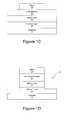
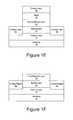
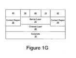
- FIGS. 1A-1Gare schematic drawings illustrating fabrication of ohmic contacts in transistors according to embodiments of the present invention.
- FIG. 2is a schematic illustration of transistors according to further embodiments of the present invention.
- FIGS. 3A and 3Bare schematic illustrations of transistors according to further embodiments of the present invention.
- FIGS. 4A-4Care schematic illustrations of fabrication of transistors according to further embodiments of the present invention.
- first, second, etc.may be used herein to describe various elements, components, regions, layers and/or sections, these elements, components, regions, layers and/or sections should not be limited by these terms. These terms are only used to distinguish one element, component, region, layer or section from another region, layer or section. Thus, a first element, component, region, layer or section discussed below could be termed a second element, component, region, layer or section without departing from the teachings of the present invention.
- relative termssuch as “lower” or “bottom” and “upper” or “top,” may be used herein to describe one element's relationship to another elements as illustrated in the Figures. It will be understood that relative terms are intended to encompass different orientations of the device in addition to the orientation depicted in the Figures. For example, if the device in the Figures is turned over, elements described as being on the “lower” side of other elements would then be oriented on “upper” sides of the other elements. The exemplary term “lower”, can therefore, encompasses both an orientation of “lower” and “upper,” depending of the particular orientation of the figure.
- Embodiments of the present inventionare described herein with reference to cross-section illustrations that are schematic illustrations of idealized embodiments of the present invention. As such, variations from the shapes of the illustrations as a result, for example, of manufacturing techniques and/or tolerances, are to be expected. Thus, embodiments of the present invention should not be construed as limited to the particular shapes of regions illustrated herein but are to include deviations in shapes that result, for example, from manufacturing. For example, an implanted region illustrated as a rectangle will, typically, have rounded or curved features and/or a gradient of implant concentration at its edges rather than a binary change from implanted to non-implanted region.
- a buried region formed by implantationmay result in some implantation in the region between the buried region and the surface through which the implantation takes place.
- the regions illustrated in the figuresare schematic in nature and their shapes are not intended to illustrate the precise shape of a region of a device and are not intended to limit the scope of the present invention.
- Embodiments of the present inventionprovide ohmic contacts on re-grown contact regions of a Group III-nitride based transistor and methods of forming such contacts.
- Embodiments of the present inventionmay be suited for use in nitride-based HEMTs such as Group III-nitride based devices.
- Group III nitriderefers to those semiconducting compounds formed between nitrogen and the elements in Group III of the periodic table, usually aluminum (Al), gallium (Ga), and/or indium (In).
- Alaluminum
- Gagallium
- Inindium
- the termalso refers to ternary and quaternary compounds such as AlGaN and AlInGaN.
- the Group III elementscan combine with nitrogen to form binary (e.g., GaN), ternary (e.g., AlGaN, AlInN), and quaternary (e.g., AlInGaN) compounds. These compounds all have empirical formulas in which one mole of nitrogen is combined with a total of one mole of the Group III elements. Accordingly, formulas such as Al x Ga 1-x N where 0 ⁇ 1 are often used to describe them.
- Suitable structures for GaN-based HEMTsthat may utilize embodiments of the present invention are described, for example, in commonly assigned U.S. Pat. No. 6,316,793 and U.S. application Ser. No. 09/904,333 filed Jul. 12, 2001 for “ALUMINUM GALLIUM NITRIDE/GALLIUM NITRIDE HIGH ELECTRON MOBILITY TRANSISTORS HAVING A GATE CONTACT ON A GALLIUM NITRIDE BASED CAP SEGMENT AND METHODS OF FABRICATING SAME,” U.S. provisional application Ser. No.
- FIGS. 1A-1GFabrication of embodiments of the present invention is schematically illustrated in FIGS. 1A-1G .
- a substrate 10is provided on which nitride based devices may be formed.
- the substrate 10may be a semi-insulating silicon carbide (SiC) substrate that may be, for example, 4H polytype of silicon carbide.
- SiCsilicon carbide
- Other silicon carbide candidate polytypesinclude the 3C, 6H, and 15R polytypes.
- the term “semi-insulating”is used descriptively rather than in an absolute sense.
- the silicon carbide bulk crystalhas a resistivity equal to or higher than about 1 ⁇ 10 5 ⁇ -cm at room temperature.
- Optional buffer, nucleation and/or transition layersmay be provided on the substrate 10 .
- an AlN buffer layermay be provided to provide an appropriate crystal structure transition between the silicon carbide substrate and the remainder of the device.
- strain balancing transition layer(s)may also be provided as described, for example, in commonly assigned U.S. patent application Ser. No. 10/199,786, filed Jul. 19, 2002 and entitled “STRAIN BALANCED NITRIDE HETROJUNCTION TRANSISTORS AND METHODS OF FABRICATING STRAIN BALANCED NITRIDE HETEROJUNCTION TRANSISTORS”, and U.S. Provisional Patent Application Ser. No. 60/337,687, filed Dec. 3, 2001 and entitled “STRAIN BALANCED NITRIDE HETEROJUNCTION TRANSISTOR,” the disclosures of which are incorporated herein by reference as if set forth fully herein.
- Silicon carbidehas a much closer crystal lattice match to Group III nitrides than does sapphire (Al 2 O 3 ), which is a very common substrate material for Group III nitride devices. The closer lattice match may result in Group III nitride films of higher quality than those generally available on sapphire. Silicon carbide also has a very high thermal conductivity so that the total output power of Group III nitride devices on silicon carbide is, typically, not as limited by thermal dissipation of the substrate as in the case of the same devices formed on sapphire. Also, the availability of semi-insulating silicon carbide substrates may provide for device isolation and reduced parasitic capacitance.
- SiC substratesare manufactured by, for example, Cree, Inc., of Durham, N.C., the assignee of the present invention, and methods for producing are described, for example, in U.S. Pat. Nos. Re. 34,861; 4,946,547; 5,200,022; and 6,218,680, the contents of which are incorporated herein by reference in their entirety.
- techniques for epitaxial growth of Group III nitrideshave been described in, for example, U.S. Pat. Nos. 5,210,051; 5,393,993; 5,523,589; and 5,292,501, the contents of which are also incorporated herein by reference in their entirety.
- silicon carbidemay be the preferred substrate material
- embodiments of the present inventionmay utilize any suitable substrate, such as sapphire, aluminum nitride, aluminum gallium nitride, gallium nitride, silicon, GaAs, LGO, ZnO, LAO, InP and the like.
- an appropriate buffer layeralso may be formed.
- a channel layer 20is provided on the substrate 10 .
- the channel layer 20may be deposited on the substrate 10 using buffer layers, transition layers, and/or nucleation layers as described above.
- the channel layer 20may be under compressive strain.
- the channel layer and/or buffer nucleation and/or transition layersmay be deposited by MOCVD or by other techniques known to those of skill in the art, such as MBE or HVPE.
- the channel layer 20is a Group III-nitride, such as Al x Ga 1-x N where 0 ⁇ 1, provided that the bandgap of the channel layer 20 is less than the bandgap of the barrier layer 22 .
- x0, indicating that the channel layer 20 is GaN.
- the channel layer 20may also be other Group III-nitrides such as InGaN, AlInGaN or the like.
- the channel layer 20may be undoped (“unintentionally doped”) and may be grown to a thickness of greater than about 20 ⁇ .
- the channel layer 20may also be a multi-layer structure, such as a superlattice or combinations of GaN, AlGaN or the like.
- a barrier layer 22is provided on the channel layer 20 .
- the channel layer 20may have a bandgap that is less than the bandgap of the barrier layer 22 .
- the barrier layer 22may be deposited on the channel layer 20 .
- the barrier layer 22is AlN, AlInN, AlGaN or AlInGaN with a thickness of between about 1 and about 100 nm.
- the barrier layer 22includes multiple layers.
- the barrier layer 22may be about 1 mm of AlN with about 25 nm of AlGaN on the AlN layer. Examples of barrier layers according to certain embodiments of the present invention are described in U.S. patent application Ser. No.
- the barrier layer 22may be a Group III-nitride and has a bandgap larger than that of the channel layer 20 . Accordingly, in certain embodiments of the present invention, the barrier layer 22 is AlGaN, AlInGaN and/or AlN or combinations of layers thereof. Other materials may also be used for the barrier layer 22 . For example, ZnGeN 2 , ZnSiN 2 and/or MgGeN 2 could also be used.
- the barrier layer 22may, for example, be from about 1 to about 100 mm thick, but is not so thick as to cause cracking or substantial defect formation therein. Preferably, the barrier layer 22 is undoped or doped with an n-type dopant to a concentration less than about 10 19 cm ⁇ 3 .
- the barrier layer 22is Al x Ga 1-x N where 0 ⁇ 1. In such embodiments, the barrier layer 22 may be from about 3 to about 30 mm thick. In particular embodiments, the aluminum concentration is about 25%. However, in other embodiments of the present invention, the barrier layer 22 comprises AlGaN with an aluminum concentration of between about 5% and about 100%. In specific embodiments of the present invention, the aluminum concentration is greater than about 10%. In embodiments of the present invention where the barrier layer 22 comprises an AlN layer, the thickness of the barrier layer 22 may, for example, be from about 0.3 nm to about 4 nm.
- FIG. 1Billustrates formation of an optional first dielectric layer 24 .
- the first dielectric layer 24may be a silicon nitride layer, such as an Si x N y layer.
- the silicon nitride layermay serve as a passivation layer for the device.
- the silicon nitride layermay be deposited by, for example, plasma-enhanced chemical vapor deposition (PECVD), low pressure chemical vapor deposition (LPCVD) and/or sputtering.
- PECVDplasma-enhanced chemical vapor deposition
- LPCVDlow pressure chemical vapor deposition
- sputteringsputtering.
- the silicon nitride layermay be deposited in the same reactor as other layers of the transistor.
- other dielectricsmay also be utilized, such as, for example, silicon oxynitride and/or silicon dioxide.
- FIG. 1Cillustrates formation of a mask 30 on the first dielectric layer 24 .
- the mask 30is formed on the region of the barrier layer 22 where a gate contact will subsequently be formed.
- the wafer of FIG. 1Cmay be removed from the epi reactor and patterned with a mask material 30 to expose the desired recess areas.
- the mask material 30should be able to withstand the growth temperature of subsequent processing, including the formation of regrown contact regions 26 as described below.
- the mask 30is provided by an oxide.
- the mask 30is patterned using lift-off techniques. Alternatively, a wet or dry etch could be utilized to pattern the mask 30 .
- SiO xis the mask material, although other materials, such as AlN and Si x N y based materials, may also be used.
- a photo-resist, e-beam resist material or organic mask materialmay also be utilized if it is not unduly damaged by subsequent processing steps, such as deposition temperatures or the like.
- the recessesare etched through the first dielectric layer 24 , through the barrier layer 22 , to the channel layer 20 and, in some embodiments, to and into the channel layer 20 or, in some embodiments, even through the channel layer 20 .
- the etch to form the contact recesses 23may be provided by, for example, a wet etch, a dry etch and/or a reactive ion etch or the like.
- the structuremay be annealed to remove and/or reduce damage resulting from the etch.
- the periphery of the devicemay be etched to form a mesa structure (not shown), for example, if other termination structures, such as a field plate, implant or other termination structure are not provided or may be provided in addition to such structures.
- a contact layer 26 ′is formed on the exposed regions of the channel layer 20 and the mask 30 .
- the wafer of FIG. 1Dmay be put back into the epi reactor for deposition of the contact layer 26 ′.
- the contact layer 26 ′is formed by metal organic chemical vapor deposition (MOCVD), molecular beam epitaxy (MBE), plasma enchanced chemical vapor deposition (PECVD), sputtering and/or hydride vapor phase epitaxy (HVPE).
- MOCVDmetal organic chemical vapor deposition
- MBEmolecular beam epitaxy
- PECVDplasma enchanced chemical vapor deposition
- HVPEhydride vapor phase epitaxy
- the contact layer 26 ′is regrown at a reduced deposition temperature. In particular, a low temperature deposition process may be used.
- low temperature depositionrefers to formation of a layer at a temperature lower than a temperature at which substantial mass transport from the wafer to the regrown region takes place.
- the contact layer 26 ′may be formed at a temperature of from about room temperature to about 950° C. In some embodiments, the contact layer 26 ′ is formed at a temperature of less than 960° C. In particular embodiments of the present invention, the contact layer 26 ′ is formed at a very low temperature, for example, at a temperature of less than about 450° C. and in some embodiments, at temperature of less than about 200° C. Such very low temperature conditions may be used, for example, with sputtering and/or PECVD growth techniques. The use of a reduced deposition temperature and/or low temperature deposition may reduce trapping and/or may provide improved reliability.
- the contact layer 26 ′may be unevenly formed such that the portion on the mask 30 is porous or discontinuous. In some embodiments, the contact layer 26 ′ is not formed on the mask 30 . Such a selective formation of the contact layer 26 ′ may depend on the composition of the contact layer 26 ′, the mask 30 and the growth conditions for the contact layer 26 ′.
- the contact layer 26 ′may be an n-type degenerate semiconductor material.
- the contact layer 26 ′may be heavily doped n-type InN, InAlN, AlGaN, AlInGaN, GaN and/or InGaN.
- the contact layer 26 ′may be an n-type degenerate semiconductor material other than GaN or AlGaN.
- the contact layermay be a non-nitride Group III-V semiconductor material, a Group IV semiconductor material and/or a Group II-VI semiconductor material.
- the contact layer 26 ′may be a metal or metal alloy, for example, a metal silicide, capable of conformal deposition at a low temperature that has a low work function and does not form a Schottky contact.
- a metal or metal alloyfor example, a metal silicide, capable of conformal deposition at a low temperature that has a low work function and does not form a Schottky contact.
- the metalmay be subsequently etched off in the channel and gate regions.
- a passivation layermay be deposited before deposition of the metal.
- Formation of a GaN contact layer 26 ′may reduce and/or eliminate a band discontinuity with the channel layer 22 if the channel layer 22 is also GaN.
- the contact layer 26 ′is formed to a thickness sufficient to provide a low sheet resistivity.
- the contact layer 26 ′may be grown to a thickness sufficient to provide a sheet resistivity that is less than a sheet resistivity of the 2DEG formed at the interface between the channel layer 20 and the barrier layer 22 .
- Several tens of nanometers of GaN, for examplemay be sufficient thickness for the contact layer 26 ′, however, a thicker layer may have a lower resistances and increase transfer length (LT).
- the contact layer 26 ′may be doped with Si, Ge and/or O or other suitable n-type dopant or may be naturally n-type as deposited.
- the contact layer 26 ′may be doped as formed rather than through subsequent ion implantation. Formation of the doped contact layer 26 ′ without ion implantation may avoid the need for extremely high temperature annealing to activate the dopants.
- the contact layer 26 ′has a sheet resistivity of from about 10 to about 400 ⁇ / ⁇ .
- the contact layeris doped to provide a carrier concentration of from about 10 18 to about 10 21 cm ⁇ 3 .
- the contact layer 26 ′is from about 10 nm to about 1000 nm thick.
- the mask 30may not be needed as the material could be blanket deposited and then patterned and etched after deposition.
- FIG. 1Fillustrates removal of the portion of the contact layer 26 ′ formed on the mask 30 and removal of the mask 30 to expose the first dielectric layer 24 , thus providing the contact regions 26 .
- the mask 30 and the portion of the contact layer 26 ′may be removed, for example, by etching the mask 30 in buffered HF or other etchant that will remove the mask layer 30 and leave the first dielectric layer 24 and the contact regions 26 .
- the portion of the contact layer 26 ′ is formed on the mask 30may be formed so as to be porous or discontinuous so as to allow etching the mask 30 through the contact layer 26 ′.
- the mask 30may be etched with an etchant that has etching selectivity with respect to the contact layer 26 ′ and the first dielectric layer 24 .
- the mask layer 30may be etched from the sides to remove the mask layer and the portion of the contact layer 26 ′ on the mask layer 30 , for example, if the portion of the contact layer 26 ′ on the mask layer is not porous or is continuous.
- FIG. 1Gillustrates formation of a gate recess in the first dielectric layer 24 and formation of a gate contact 44 on the exposed portion of the barrier layer 22 in the gate recess.
- a gate recessmay be etched through the first dielectric layer 24 using, for example, a dry etch, a wet etch and/or RIE or the like.
- the structuremay be annealed to repair some or all of the damage resulting from the etch of the gate recess.
- Suitable gate contact materialsinclude, for example, Ni, Pt, Pd or other such Schottky contact materials. Additional overlayers may also be provided.
- the gate contact 44may be formed on the dielectric layer 24 .
- ohmic contacts 40 and 42are formed on the contact regions 26 and may provide source and drain contacts.
- the ohmic contacts 40 and 42may be formed before or after formation of the gate recess and/or contact 44 .
- the ohmic contacts 40 and 42are annealed, for example at a temperature of about 850° C. or less. In other embodiments, the anneal of the ohmic contacts is not carried out. The use of a reduced anneal temperature or no anneal may reduce trapping and/or may provided improved reliability.
- the presence of the highly doped n-type contact regionsmay lower contact resistance that may provide for increased efficiency and/or radio frequency power density.
- Suitable ohmic contact materialsinclude, for example, a Ti/Al/Ni/Au stack may be used. Similarly, a structure of Ti/AI/X/Au may be used where X may be Mo, Pt and/or Ti.
- the gate recess and gate contactmay be formed before or after formation of the ohmic contacts or even before formation of the contact recesses. Accordingly, embodiments of the present invention should not be construed as limited to the specific sequence of operations described above.
- FIGS. 2, 3A and 3 Bare illustrations of embodiments of the present invention incorporating contact area enlargement structures that provide increased vertical surface area of the interface between the contact region 26 and the channel layer 20 .
- FIG. 2illustrates embodiments of the present invention as incorporating a contact area enlargement area structure in a sidewall of a portion of the channel layer 20 and
- FIGS. 3A and 3Billustrate embodiments of the present invention where the contact enlargement area structure is provided by filled holes extending into the contact layer 20 .
- the contact area enlargement structuresmay also be provided in combination with each other or other structures that increase the vertical contact area between the channel layer 20 and the contact region 26 as compared to a planar vertical contact area.
- Such structuresmay provide means for increasing a surface area of an interface between a vertical portion of the n-type nitride-based semiconductor material contact region 26 and the nitride-based channel layer 20 .
- FIGS. 2, 3A and 3 Billustrate a partial section of a transistor illustrating a single ohmic contact region.
- a corresponding sectionmay be provided for a second ohmic contact region opposite the gate contact so as to provide source and drain contacts.
- embodiments of the present inventionmay provide a contact area enlargement structure for only one of the ohmic contacts.
- FIG. 2is a top view of a portion of a HEMT according to further embodiments of the present invention.
- the surface area of the interface between the contact region 26 and the channel layer 20 and/or the barrier layer 22may be increased by providing an increased surface area sidewall 200 of the channel layer 20 and/or the barrier layer 22 .
- the increased surface area sidewall 200has an increased surface area with respect to a straight sidewall. Increasing the surface area of the interface between the contact region 26 and the channel layer 20 may reduce the resistance between the contact region 26 and the channel layer 20 .
- the patterned sidewall 200may be provided by patterning the channel layer 20 during the contact recess etch described above. For example, a first etch through the first dielectric layer 24 and the barrier layer 22 may be performed and then a second etch into the channel layer 22 may be performed with a mask on the exposed portion of the channel layer 20 to provide the pattern of the sidewall. Alternatively, a single etch may be performed if the mask 30 has a pattern corresponding to the desired sidewall pattern of the channel layer 20 .
- the sidewallmay have a regular or irregular repeating or non-repeating shape.
- the sawtooth shape illustrated in FIG. 2is provided as an example of a shape that may be used. However, other shapes may also be used, for example, a notch shape, a series of curves or the like may be used. Accordingly, some embodiments of the present invention should not be limited to a particular shape for the increased surface area sidewall 200 .
- the ohmic contact metal 42 ′is also illustrated in FIG. 2 on the contact region 26 .
- the contact metal 42 ′is illustrated as stopping before the periphery of the contact region 26 .
- the contact metal 42 ′may extend further than illustrated and may, for example, extend onto the channel layer 22 .
- FIG. 3Ais a top view and FIG. 3B is a cross-section taken along the lines I-I′ of FIG. 3A of further embodiments of the present invention.
- the surface area of the interface between the regrown contact region 26 and the channel layer 20may be increased by providing holes 300 that extend into the channel layer 20 .
- the holes 300have n-type material in them as provided in the contact region 26 .
- the ohmic contact 42 ′′extends to cover the holes 300 so that the n-type material in the holes 300 is electrically connected to the contact region 26 .
- the filled holes 300may be provided by patterning the channel layer 20 during the contact recess etch described above so as to provide holes that are present when the contact layer 26 ′ is formed. For example, a first etch through the first dielectric layer 24 and the barrier layer 22 may be performed and then a second etch into the channel layer 22 may be performed with a mask on the exposed portion to the channel layer 20 to provide the holes.
- a single etchmay be performed if the mask 30 has a pattern corresponding to the desired holes of the channel layer 20 .
- the holeswould extend through the barrier layer 22 and to or into the channel layer 20 .
- the contact metalwould then extend onto the barrier layer 22 to contact the material in the holes 300 as illustrated in FIG. 3B .
- the holes 300may have a regular or irregular repeating or non-repeating pattern. Furthermore, the holes 300 may also have a circular or other shape periphery.
- the pattern of holes and shape of holes illustrated in FIG. 3Ais provided as an example of a pattern and shape that may be used. However, other patterns and/or shapes may also be used. Accordingly, some embodiments of the present invention should not be limited to a particular pattern and/or shape for the holes 300 .
- FIGS. 4A-4Cillustrate fabrication of further embodiments of the present invention where a contact region is provided that extends onto the barrier layer. Fabrication of the embodiments of the present invention illustrated in FIGS. 4A-4C may be the same as that illustrated in FIGS. 1A-1F except that the first dielectric layer 24 is resized to a smaller size first dielectric layer 424 so as to expose a portion of the barrier layer 22 , for example, by undercutting the mask 30 into the first dielectric layer 24 with an isotropic etch. Alternatively, the mask 30 could be stripped and another mask applied and the first dielectric layer 24 may be etched using this second mask. While the first dielectric layer 424 in FIG. 4A is described herein as a dielectric material, other removable materials that may withstand the conditions for deposition of the contact regions may be used.
- the contact region 426is regrown as discussed above and the mask 30 is removed.
- the first dielectric layer 424is removed and a second dielectric layer 430 is conformally deposited on the contact layers 426 and the barrier layer 22 .
- the second dielectric layer 430would typically be deposited isotropically. Windows in the second dielectric layer 430 may be provided on the contact layer 426 and ohmic contacts for the source and drain contacts 440 and 442 may be formed on the contact layer 426 .
- the ohmic contactsmay also be formed prior to the deposition of the second dielectric layer 430 .
- the second dielectric layer 430is anisotropically etched to expose the barrier layer 22 and provide sidewall spaces 430 ′ and a gate contact recess.
- a gate metalmay be deposited and patterned, for example, using lift-off techniques, to provided the gate contact 444 .
- the length of the gate contact 444may be approximately the width of the first dielectic layer 424 less twice the thickness of the second dielectric layer 430 .
- the first dielectric 424may have a width of about 0.5 to about 1 ⁇ m and the second dielectric 430 may have a thickness of from about 0.1 to about 0.5 ⁇ m.
- regrown contact regionsfor both the source and drain contacts
- regrown regionsmay be provided for only one of the source or the drain.
- the gate contactshave been illustrated as substantially centered between the source and drain, in certain embodiments of the present invention, the gate contact may be offset, for example, toward the source contact.
Landscapes
- Junction Field-Effect Transistors (AREA)
- Electrodes Of Semiconductors (AREA)
Abstract
Description
- The present invention relates to semiconductor devices and, more particularly, to transistors that incorporate nitride-based active layers.
- The present invention relates to transistors formed of semiconductor materials that can make them suitable for high power, high temperature, and/or high frequency applications. Materials such as silicon (Si) and gallium arsenide (GaAs) have found wide application in semiconductor devices for lower power and (in the case of Si) lower frequency applications. These, more familiar, semiconductor materials may not be well suited for higher power and/or high frequency applications, however, because of their relatively small bandgaps (e.g., 1.12 eV for Si and 1.42 for GaAs at room temperature) and/or relatively small breakdown voltages.
- In light of the difficulties presented by Si and GaAs, interest in high power, high temperature and/or high frequency applications and devices has turned to wide bandgap semiconductor materials such as silicon carbide (2.996 eV for alpha SiC at room temperature) and the Group III nitrides (e.g., 3.36 eV for GaN at room temperature). These materials, typically, have higher electric field breakdown strengths and higher electron saturation velocities as compared to gallium arsenide and silicon.
- A device of particular interest for high power and/or high frequency applications is the High Electron Mobility Transistor (HEMT), which is also known as a modulation doped field effect transistor (MODFET). These devices may offer operational advantages under a number of circumstances because a two-dimensional electron gas (2DEG) is formed at the heterojunction of two semiconductor materials with different bandgap energies, and where the smaller bandgap material has a higher electron affinity. The 2DEG is an accumulation layer in the undoped (“unintentionally doped”), smaller bandgap material and can contain a very high sheet electron concentration in excess of, for example, 1013carriers/cm2. Additionally, electrons that originate in the wider-bandgap semiconductor transfer to the 2DEG, allowing a high electron mobility due to reduced ionized impurity scattering.
- This combination of high carrier concentration and high carrier mobility can give the HEMT a very large transconductance and may provide a strong performance advantage over metal-semiconductor field effect transistors (MESFETs) for high-frequency applications.
- High electron mobility transistors fabricated in the gallium nitride/aluminum gallium nitride (GaN/AlGaN) material system have the potential to generate large amounts of RF power because of the combination of material characteristics that includes the aforementioned high breakdown fields, their wide bandgaps, large conduction band offset, and/or high saturated electron drift velocity. A major portion of the electrons in the 2DEG is attributed to polarization in the AlGaN. HEMTs in the GaN/AlGaN system have already been demonstrated. U.S. Pat. Nos. 5,192,987 and 5,296,395 describe AlGaN/GaN HEMT structures and methods of manufacture. U.S. Pat. No. 6,316,793, to Sheppard et al., which is commonly assigned and is incorporated herein by reference, describes a HEMT device having a semi-insulating silicon carbide substrate, an aluminum nitride buffer layer on the substrate, an insulating gallium nitride layer on the buffer layer, an aluminum gallium nitride barrier layer on the gallium nitride layer, and a passivation layer on the aluminum gallium nitride active structure.
- One issue with the fabrication of nitride-based transistors involves the formation of ohmic contacts for such transistors. Conventionally, ohmic contacts have been formed through reactive ion etching (RIE) recesses for the contacts. However, without strict process control practices, RIE in nitride based materials may suffer from uniformity and reproducibility problems. Such problems could result in difficulty in controlling a fabrication process. Ohmic contacts that are formed without RIE have, typically, used high annealing temperatures (e.g. 900° C.). Such high annealing temperatures may damage the materials and/or the device.
- Some embodiments of the present invention provide for fabrication of a transistor including forming a nitride-based channel layer on a substrate, forming a barrier layer on the nitride-based channel layer, forming a contact recess in the barrier layer to expose a contact region of the nitride-based channel layer and forming a contact layer on the exposed contact region of the nitride-based channel layer using a low temperature deposition process. Fabrication may also include forming an ohmic contact on the contact layer and forming a gate contact disposed on the barrier layer adjacent the ohmic contact.
- In further embodiments of the present invention, forming a contact layer on the exposed contact region of the nitride-based channel layer using a low temperature deposition process includes forming a contact layer by metal organic chemical vapor deposition (MOCVD), molecular beam epitaxy (MBE), plasma enchanced chemical vapor deposition (PECVD), sputtering and/or hydride vapor phase epitaxy (HVPE). Furthermore, the low temperature deposition process may be a process other than mass transport from a wafer on which the transistor is formed.
- In additional embodiments of the present invention, fabrication of the transistor further includes forming a first dielectric layer on the barrier layer and forming a recess in the first dielectric layer. Forming a gate contact includes forming a gate contact in the recess. Forming a contact recess includes forming a contact recess in the first dielectric layer and the barrier layer that exposes a portion of the nitride-based channel layer. In other embodiments of the present invention, the gate contact may be formed on the first dielectric layer.
- In still further embodiments of the present invention, the first dielectric layer comprises a silicon nitride layer. The silicon nitride layer may provide a passivation layer for the transistor.
- In additional embodiments of the present invention, the contact recess extends into the channel layer. Furthermore, forming an ohmic contact may include forming an ohmic contact without annealing the ohmic contact. Forming an ohmic contact could include patterning a metal layer on the contact layer and annealing the patterned metal layer at a temperature of about 850° C. or less.
- In other embodiments of the present invention, forming a contact layer on the exposed portions of the nitride-based channel layer includes forming a contact layer on the exposed portion of the nitride-based channel layer to a thickness sufficient to provide a sheet resistivity of less than a sheet resistivity of a two-dimensional electron gas region formed at an interface between the channel layer and the barrier layer. Forming a contact layer may include forming n-type an InGaN, AlInN, AlInGaN and/or InN layer. In some embodiments of the present invention, the n-type nitride-based layer formed is GaN and/or AlGaN. The InGaN, GaN, AlGaN, AlInN, AlInGaN and/or InN layer may be doped with Si, Ge and/or O during formation.
- In some embodiments of the present invention, the contact layer includes an n-type degenerate semiconductor material other than GaN and AlGaN. The contact layer may include a non-nitride Group III-V semiconductor material, a Group IV semiconductor material and/or a group III-VI semiconductor material.
- In additional embodiments of the present invention, fabrication of the transistor further includes forming sidewalls of the channel layer to provide an increased surface area interface between the channel layer and the n-type contact layer as compared to a planar interface. Forming an ohmic contact on the contact layer may include forming an ohmic contact on the contact layer that extends onto a portion of the channel layer or that terminates before the sidewall of the channel layer.
- In further embodiments of the present invention, fabrication of the transistor includes forming holes in the channel layer adjacent the contact regions and placing n-type nitride-based semiconductor material in the holes. Forming an ohmic contact on the contact layer further includes forming an ohmic contact on the contact layer and on the nitride-based semiconductor material in the holes.
- In additional embodiments of the present invention, the contact layer extends onto the barrier layer.
- In still other embodiments of the present invention, fabricating a transistor includes forming a nitride-based channel layer on a substrate, forming a barrier layer on the nitride-based channel layer, forming a masking layer on the barrier layer, patterning the masking layer and the barrier layer to provide contact opening that exposes a portion of the nitride-based channel layer, forming a contact layer on the exposed portion of the nitride-based channel layer and the masking layer, selectively removing the masking layer and a portion of the contact layer on the masking layer to provide a contact region, forming an ohmic contact on the contact region and forming a gate contact disposed on the barrier layer adjacent the ohmic contact. Fabrication of the transistor may also include forming a first dielectric layer on the barrier layer and forming a recess in the first dielectric layer. Forming a gate contact may include forming a gate contact in the recess. Forming a masking layer on the barrier layer may include forming a masking layer on the first dielectric layer. Patterning the masking layer and the barrier layer to provide contact openings that expose a portion of the nitride-based channel layer may include patterning the masking layer, the first dielectric layer and the barrier layer to provide contact opening that exposes a portion of the nitride-based channel layer.
- In certain embodiments of the present invention, the first dielectric layer includes a silicon nitride layer. The silicon nitride layer may provide a passivation layer for the transistor. The masking layer may be a dielectric layer. The dielectric layer may be a silicon oxide layer. The masking layer could be a photoresist masking layer.
- Forming an ohmic contact may be provided by forming an ohmic contact without annealing the ohmic contact. Alternatively, forming an ohmic contact may be provided by patterning a metal layer on the contact region and annealing the patterned metal layer at a temperature of about 850° C. or less.
- Forming a contact layer on the exposed portion of the nitride-based channel layer and the oxide layer may include forming a contact layer by metal organic chemical vapor deposition (MOCVD), molecular beam epitaxy (MBE), plasma enhanced chemical vapor deposition (PECVD), sputtering and/or hydride vapor phase epitaxy (HVPE). Forming a contact layer on the exposed portions of the nitride-based channel layer and the masking layer may be provided by forming a contact layer on the exposed portions of the nitride-based channel layer and the masking layer to a thickness sufficient to provide a sheet resistivity of less than a sheet resistivity of a two-dimensional electron gas region formed at an interface between the channel layer and the barrier layer. Forming a contact layer may include forming an n-type InGaN, AlInGaN, InAlN and/or InN layer. In some embodiments, the nitride based contact layer may be GaN and/or AlGaN. The InGaN, AlInGaN, InAlN, GaN, AlGaN and/or InN layer may be doped with Si, Ge and/or O during formation.
- In further embodiments of the present invention, fabrication of the transistor includes forming sidewalls of the channel layer to provide an increased surface area interface between the channel layer and the n-type contact layer compared to a planar interface. Forming an ohmic contact on the contact layer may include forming an ohmic contact on the contact layer that extends onto a portion of the channel layer or that terminates before the sidewall of the channel layer. Additionally or alternatively, fabrication of the transistor may include forming holes in the channel layer adjacent the contact regions and placing a nitride-based semiconductor material in the holes. Forming an ohmic contact on the nitride-based contact region may include forming an ohmic contact on the nitride-based contact region and on the nitride-based semiconductor material in the holes.
- In other embodiments of the present invention, a high electron mobility transistor (HEMT) and methods of fabricating a HEMT are provided. The HEMT includes a nitride-based channel layer on a substrate, a barrier layer on the nitride-based channel layer, a contact recess in the barrier layer that extends into the channel layer, a contact region on the nitride-based channel layer in the contact recess, a gate contact disposed on the barrier layer. The contact region and the nitride-based channel layer include a surface area enlargement structure.
- In some embodiments of the present invention, the surface area enlargement structure includes patterned sidewalls of portions of the contact recess that extends into the channel layer. In certain embodiments of the present invention, an ohmic contact is provided on the contact region that does not extend onto the channel layer in the area of the sidewalls. In other embodiments of the present invention, the ohmic contact extends onto the channel layer in the area of the sidewalls.
- In additional embodiments of the present invention, the surface area enlargement structure includes holes extending into the channel layer with n-type nitride-based semiconductor material in the and the ohmic contact is in contact with the nitride-based semiconductor material in the holes.
- The n-type nitride-based semiconductor material may include InN, AlGaN, InGaN, AlInGaN, AlInN and/or GaN. The n-type nitride-based semiconductor material may be doped with Si, Ge and/or O. A silicon nitride layer may also be provided on the barrier layer and the gate contact may be provided in a recess in the silicon nitride layer.
- Further embodiments of the present invention provide a high electron mobility transistor and methods of fabricating a transistor that includes a nitride-based channel layer on a substrate and a barrier layer on the nitride-based channel layer. At least one contact recess is provided in the barrier layer that extends into the channel layer. A region of metal and/or metal alloy is provided on the nitride-based channel layer in the contact recess to provide an ohmic contact. A gate contact disposed is on the barrier layer. The region of metal may extend onto the barrier layer.
- Additional embodiments of the present invention provide a high electron mobility transistor and methods of fabricating a transistor that includes a nitride-based channel layer on a substrate and a barrier layer on the nitride-based channel layer. At least one contact recess is provided in the barrier layer that extends into the channel layer. A region of n-type degenerate semiconductor material other than GaN or AlGaN is provided on the nitride-based channel layer in the contact recess. An ohmic contact is provided on the region of n-type degenerate semiconductor material and a gate contact is disposed on the barrier layer. The region of n-type degenerate semiconductor material may extend onto the barrier layer.
FIGS. 1A-1G are schematic drawings illustrating fabrication of ohmic contacts in transistors according to embodiments of the present invention.FIG. 2 is a schematic illustration of transistors according to further embodiments of the present invention.FIGS. 3A and 3B are schematic illustrations of transistors according to further embodiments of the present invention.FIGS. 4A-4C are schematic illustrations of fabrication of transistors according to further embodiments of the present invention.- The present invention now will be described more fully hereinafter with reference to the accompanying drawings, in which embodiments of the invention are shown. This invention may, however, be embodied in many different forms and should not be construed as limited to the embodiments set forth herein. Rather, these embodiments are provided so that this disclosure will be thorough and complete, and will fully convey the scope of the invention to those skilled in the art. In the drawings, the size and relative sizes of layers and regions may be exaggerated for clarity. It will be understood that when an element or layer is referred to as being “on”, “connected to” or “coupled to” another element or layer, it can be directly on, connected or coupled to the other element or layer or intervening elements or layers may be present. In contrast, when an element is referred to as being “directly on,” “directly connected to” or “directly coupled to” another element or layer, there are no intervening elements or layers present. Like numbers refer to like elements throughout. As used herein, the term “and/or” includes any and all combinations of one or more of the associated listed items.
- It will be understood that, although the terms first, second, etc. may be used herein to describe various elements, components, regions, layers and/or sections, these elements, components, regions, layers and/or sections should not be limited by these terms. These terms are only used to distinguish one element, component, region, layer or section from another region, layer or section. Thus, a first element, component, region, layer or section discussed below could be termed a second element, component, region, layer or section without departing from the teachings of the present invention.
- Furthermore, relative terms, such as “lower” or “bottom” and “upper” or “top,” may be used herein to describe one element's relationship to another elements as illustrated in the Figures. It will be understood that relative terms are intended to encompass different orientations of the device in addition to the orientation depicted in the Figures. For example, if the device in the Figures is turned over, elements described as being on the “lower” side of other elements would then be oriented on “upper” sides of the other elements. The exemplary term “lower”, can therefore, encompasses both an orientation of “lower” and “upper,” depending of the particular orientation of the figure. Similarly, if the device in one of the figures is turned over, elements described as “below” or “beneath” other elements would then be oriented “above” the other elements. The exemplary terms “below” or “beneath” can, therefore, encompass both an orientation of above and below.
- Embodiments of the present invention are described herein with reference to cross-section illustrations that are schematic illustrations of idealized embodiments of the present invention. As such, variations from the shapes of the illustrations as a result, for example, of manufacturing techniques and/or tolerances, are to be expected. Thus, embodiments of the present invention should not be construed as limited to the particular shapes of regions illustrated herein but are to include deviations in shapes that result, for example, from manufacturing. For example, an implanted region illustrated as a rectangle will, typically, have rounded or curved features and/or a gradient of implant concentration at its edges rather than a binary change from implanted to non-implanted region. Likewise, a buried region formed by implantation may result in some implantation in the region between the buried region and the surface through which the implantation takes place. Thus, the regions illustrated in the figures are schematic in nature and their shapes are not intended to illustrate the precise shape of a region of a device and are not intended to limit the scope of the present invention.
- Embodiments of the present invention provide ohmic contacts on re-grown contact regions of a Group III-nitride based transistor and methods of forming such contacts.
- Embodiments of the present invention may be suited for use in nitride-based HEMTs such as Group III-nitride based devices. As used herein, the term “Group III nitride” refers to those semiconducting compounds formed between nitrogen and the elements in Group III of the periodic table, usually aluminum (Al), gallium (Ga), and/or indium (In). The term also refers to ternary and quaternary compounds such as AlGaN and AlInGaN. As is well understood by those in this art, the Group III elements can combine with nitrogen to form binary (e.g., GaN), ternary (e.g., AlGaN, AlInN), and quaternary (e.g., AlInGaN) compounds. These compounds all have empirical formulas in which one mole of nitrogen is combined with a total of one mole of the Group III elements. Accordingly, formulas such as AlxGa1-xN where 0≦×≦1 are often used to describe them.
- Suitable structures for GaN-based HEMTs that may utilize embodiments of the present invention are described, for example, in commonly assigned U.S. Pat. No. 6,316,793 and U.S. application Ser. No. 09/904,333 filed Jul. 12, 2001 for “ALUMINUM GALLIUM NITRIDE/GALLIUM NITRIDE HIGH ELECTRON MOBILITY TRANSISTORS HAVING A GATE CONTACT ON A GALLIUM NITRIDE BASED CAP SEGMENT AND METHODS OF FABRICATING SAME,” U.S. provisional application Ser. No. 60/290,195 filed May 11, 2001 for “GROUP III NITRIDE BASED HIGH ELECTRON MOBILITY TRANSISTOR (HEMT) WITH BARRIER/SPACER LAYER” and U.S. patent application Ser. No. 10/102,272, to Smorchkova et al., entitled “GROUP-III NITRIDE BASED HIGH ELECTRON MOBILITY TRANSISTOR (HEMT) WITH BARRIER/SPACER LAYER” the disclosures of which are hereby incorporated herein by reference in their entirety.
- Fabrication of embodiments of the present invention is schematically illustrated in
FIGS. 1A-1G . As seen inFIG. 1A , asubstrate 10 is provided on which nitride based devices may be formed. In particular embodiments of the present invention, thesubstrate 10 may be a semi-insulating silicon carbide (SiC) substrate that may be, for example, 4H polytype of silicon carbide. Other silicon carbide candidate polytypes include the 3C, 6H, and 15R polytypes. The term “semi-insulating” is used descriptively rather than in an absolute sense. In particular embodiments of the present invention, the silicon carbide bulk crystal has a resistivity equal to or higher than about 1×10⁵Ω-cm at room temperature. - Optional buffer, nucleation and/or transition layers (not shown) may be provided on the
substrate 10. For example, an AlN buffer layer may be provided to provide an appropriate crystal structure transition between the silicon carbide substrate and the remainder of the device. Additionally, strain balancing transition layer(s) may also be provided as described, for example, in commonly assigned U.S. patent application Ser. No. 10/199,786, filed Jul. 19, 2002 and entitled “STRAIN BALANCED NITRIDE HETROJUNCTION TRANSISTORS AND METHODS OF FABRICATING STRAIN BALANCED NITRIDE HETEROJUNCTION TRANSISTORS”, and U.S. Provisional Patent Application Ser. No. 60/337,687, filed Dec. 3, 2001 and entitled “STRAIN BALANCED NITRIDE HETEROJUNCTION TRANSISTOR,” the disclosures of which are incorporated herein by reference as if set forth fully herein. - Silicon carbide has a much closer crystal lattice match to Group III nitrides than does sapphire (Al2O3), which is a very common substrate material for Group III nitride devices. The closer lattice match may result in Group III nitride films of higher quality than those generally available on sapphire. Silicon carbide also has a very high thermal conductivity so that the total output power of Group III nitride devices on silicon carbide is, typically, not as limited by thermal dissipation of the substrate as in the case of the same devices formed on sapphire. Also, the availability of semi-insulating silicon carbide substrates may provide for device isolation and reduced parasitic capacitance. Appropriate SiC substrates are manufactured by, for example, Cree, Inc., of Durham, N.C., the assignee of the present invention, and methods for producing are described, for example, in U.S. Pat. Nos. Re. 34,861; 4,946,547; 5,200,022; and 6,218,680, the contents of which are incorporated herein by reference in their entirety. Similarly, techniques for epitaxial growth of Group III nitrides have been described in, for example, U.S. Pat. Nos. 5,210,051; 5,393,993; 5,523,589; and 5,292,501, the contents of which are also incorporated herein by reference in their entirety.
- Although silicon carbide may be the preferred substrate material, embodiments of the present invention may utilize any suitable substrate, such as sapphire, aluminum nitride, aluminum gallium nitride, gallium nitride, silicon, GaAs, LGO, ZnO, LAO, InP and the like. In some embodiments, an appropriate buffer layer also may be formed.
- Returning to
FIG. 1A , achannel layer 20 is provided on thesubstrate 10. Thechannel layer 20 may be deposited on thesubstrate 10 using buffer layers, transition layers, and/or nucleation layers as described above. Thechannel layer 20 may be under compressive strain. Furthermore, the channel layer and/or buffer nucleation and/or transition layers may be deposited by MOCVD or by other techniques known to those of skill in the art, such as MBE or HVPE. - In some embodiments of the present invention, the
channel layer 20 is a Group III-nitride, such as AlxGa1-xN where 0≦×<1, provided that the bandgap of thechannel layer 20 is less than the bandgap of thebarrier layer 22. In certain embodiments of the present invention, x=0, indicating that thechannel layer 20 is GaN. Thechannel layer 20 may also be other Group III-nitrides such as InGaN, AlInGaN or the like. Thechannel layer 20 may be undoped (“unintentionally doped”) and may be grown to a thickness of greater than about 20 Å. Thechannel layer 20 may also be a multi-layer structure, such as a superlattice or combinations of GaN, AlGaN or the like. - A
barrier layer 22 is provided on thechannel layer 20. Thechannel layer 20 may have a bandgap that is less than the bandgap of thebarrier layer 22. Thebarrier layer 22 may be deposited on thechannel layer 20. In certain embodiments of the present invention, thebarrier layer 22 is AlN, AlInN, AlGaN or AlInGaN with a thickness of between about 1 and about 100 nm. In some embodiments of the present invention, thebarrier layer 22 includes multiple layers. For example, thebarrier layer 22 may be about 1 mm of AlN with about 25 nm of AlGaN on the AlN layer. Examples of barrier layers according to certain embodiments of the present invention are described in U.S. patent application Ser. No. 10/102,272, to Smorchkova et al., entitled “GROUP-III NITRIDE BASED HIGH ELECTRON MOBILITY TRANSISTOR (HEMT) WITH BARRIER/SPACER LAYER” the disclosure of which is incorporated herein by reference as if set forth fully herein. - The
barrier layer 22 may be a Group III-nitride and has a bandgap larger than that of thechannel layer 20. Accordingly, in certain embodiments of the present invention, thebarrier layer 22 is AlGaN, AlInGaN and/or AlN or combinations of layers thereof. Other materials may also be used for thebarrier layer 22. For example, ZnGeN2, ZnSiN2and/or MgGeN2could also be used. Thebarrier layer 22 may, for example, be from about 1 to about 100 mm thick, but is not so thick as to cause cracking or substantial defect formation therein. Preferably, thebarrier layer 22 is undoped or doped with an n-type dopant to a concentration less than about 1019cm−3. In some embodiments of the present invention, thebarrier layer 22 is AlxGa1-xN where 0<×<1. In such embodiments, thebarrier layer 22 may be from about 3 to about 30 mm thick. In particular embodiments, the aluminum concentration is about 25%. However, in other embodiments of the present invention, thebarrier layer 22 comprises AlGaN with an aluminum concentration of between about 5% and about 100%. In specific embodiments of the present invention, the aluminum concentration is greater than about 10%. In embodiments of the present invention where thebarrier layer 22 comprises an AlN layer, the thickness of thebarrier layer 22 may, for example, be from about 0.3 nm to about 4 nm. FIG. 1B illustrates formation of an optional firstdielectric layer 24. Thefirst dielectric layer 24 may be a silicon nitride layer, such as an SixNylayer. The silicon nitride layer may serve as a passivation layer for the device. The silicon nitride layer may be deposited by, for example, plasma-enhanced chemical vapor deposition (PECVD), low pressure chemical vapor deposition (LPCVD) and/or sputtering. The silicon nitride layer may be deposited in the same reactor as other layers of the transistor. In some embodiments of the present invention, other dielectrics may also be utilized, such as, for example, silicon oxynitride and/or silicon dioxide.FIG. 1C illustrates formation of amask 30 on thefirst dielectric layer 24. Themask 30 is formed on the region of thebarrier layer 22 where a gate contact will subsequently be formed. As illustrated inFIG. 1C , the wafer ofFIG. 1C may be removed from the epi reactor and patterned with amask material 30 to expose the desired recess areas. Themask material 30 should be able to withstand the growth temperature of subsequent processing, including the formation ofregrown contact regions 26 as described below. In particular embodiments of the present invention, themask 30 is provided by an oxide. In certain embodiments of the present invention, themask 30 is patterned using lift-off techniques. Alternatively, a wet or dry etch could be utilized to pattern themask 30. In certain embodiments of the present invention, SiOxis the mask material, although other materials, such as AlN and SixNybased materials, may also be used. A photo-resist, e-beam resist material or organic mask material may also be utilized if it is not unduly damaged by subsequent processing steps, such as deposition temperatures or the like.- As illustrated in
FIG. 1D , after formation and patterning of themask 30 so as to leave the mask material in the regions where contact recesses23 are not to be formed for the ohmic contacts, the recesses are etched through thefirst dielectric layer 24, through thebarrier layer 22, to thechannel layer 20 and, in some embodiments, to and into thechannel layer 20 or, in some embodiments, even through thechannel layer 20. The etch to form the contact recesses23 may be provided by, for example, a wet etch, a dry etch and/or a reactive ion etch or the like. Optionally, the structure may be annealed to remove and/or reduce damage resulting from the etch. Furthermore, optionally, the periphery of the device may be etched to form a mesa structure (not shown), for example, if other termination structures, such as a field plate, implant or other termination structure are not provided or may be provided in addition to such structures. - As illustrated in
FIG. 1E , after etching the contact recesses23, acontact layer 26′ is formed on the exposed regions of thechannel layer 20 and themask 30. For example, the wafer ofFIG. 1D may be put back into the epi reactor for deposition of thecontact layer 26′. In some embodiments of the present invention, thecontact layer 26′ is formed by metal organic chemical vapor deposition (MOCVD), molecular beam epitaxy (MBE), plasma enchanced chemical vapor deposition (PECVD), sputtering and/or hydride vapor phase epitaxy (HVPE). In some embodiments, thecontact layer 26′ is regrown at a reduced deposition temperature. In particular, a low temperature deposition process may be used. As used herein “low temperature deposition” refers to formation of a layer at a temperature lower than a temperature at which substantial mass transport from the wafer to the regrown region takes place. For example, thecontact layer 26′ may be formed at a temperature of from about room temperature to about 950° C. In some embodiments, thecontact layer 26′ is formed at a temperature of less than 960° C. In particular embodiments of the present invention, thecontact layer 26′ is formed at a very low temperature, for example, at a temperature of less than about 450° C. and in some embodiments, at temperature of less than about 200° C. Such very low temperature conditions may be used, for example, with sputtering and/or PECVD growth techniques. The use of a reduced deposition temperature and/or low temperature deposition may reduce trapping and/or may provide improved reliability. - As discussed below, the
contact layer 26′ may be unevenly formed such that the portion on themask 30 is porous or discontinuous. In some embodiments, thecontact layer 26′ is not formed on themask 30. Such a selective formation of thecontact layer 26′ may depend on the composition of thecontact layer 26′, themask 30 and the growth conditions for thecontact layer 26′. - In some embodiments of the present invention, the
contact layer 26′ may be an n-type degenerate semiconductor material. In certain embodiments of the present invention, thecontact layer 26′ may be heavily doped n-type InN, InAlN, AlGaN, AlInGaN, GaN and/or InGaN. In other embodiments of the present invention, thecontact layer 26′ may be an n-type degenerate semiconductor material other than GaN or AlGaN. For example, the contact layer may be a non-nitride Group III-V semiconductor material, a Group IV semiconductor material and/or a Group II-VI semiconductor material. Examples ofpotential contact layer 26′ materials include, for example, ZnO, ZnGeN2and/or ZnSnN2. In other embodiments of the present invention, thecontact layer 26′ may be a metal or metal alloy, for example, a metal silicide, capable of conformal deposition at a low temperature that has a low work function and does not form a Schottky contact. For example, an MOCVD conformal deposition of Al using DMAlH at a temperature of at least about 200° C. to touch the 2DEG. The metal may be subsequently etched off in the channel and gate regions. Furthermore, a passivation layer may be deposited before deposition of the metal. - Formation of a
GaN contact layer 26′ may reduce and/or eliminate a band discontinuity with thechannel layer 22 if thechannel layer 22 is also GaN. Thecontact layer 26′ is formed to a thickness sufficient to provide a low sheet resistivity. For example, thecontact layer 26′ may be grown to a thickness sufficient to provide a sheet resistivity that is less than a sheet resistivity of the 2DEG formed at the interface between thechannel layer 20 and thebarrier layer 22. Several tens of nanometers of GaN, for example, may be sufficient thickness for thecontact layer 26′, however, a thicker layer may have a lower resistances and increase transfer length (LT). Thecontact layer 26′ may be doped with Si, Ge and/or O or other suitable n-type dopant or may be naturally n-type as deposited. Thecontact layer 26′ may be doped as formed rather than through subsequent ion implantation. Formation of the dopedcontact layer 26′ without ion implantation may avoid the need for extremely high temperature annealing to activate the dopants. In particular embodiments of the present invention, thecontact layer 26′ has a sheet resistivity of from about 10 to about 400 Ω/□. In certain embodiments of the present invention, the contact layer is doped to provide a carrier concentration of from about 1018to about 1021cm−3. In still further embodiments of the present invention, thecontact layer 26′ is from about 10 nm to about 1000 nm thick. - For a
contact layer 26′ that is not a Group III nitride material, themask 30 may not be needed as the material could be blanket deposited and then patterned and etched after deposition. FIG. 1F illustrates removal of the portion of thecontact layer 26′ formed on themask 30 and removal of themask 30 to expose thefirst dielectric layer 24, thus providing thecontact regions 26. Themask 30 and the portion of thecontact layer 26′ may be removed, for example, by etching themask 30 in buffered HF or other etchant that will remove themask layer 30 and leave thefirst dielectric layer 24 and thecontact regions 26. In some embodiments of the present invention, the portion of thecontact layer 26′ is formed on themask 30 may be formed so as to be porous or discontinuous so as to allow etching themask 30 through thecontact layer 26′. In such a way, themask 30 may be etched with an etchant that has etching selectivity with respect to thecontact layer 26′ and thefirst dielectric layer 24. For smaller geometry devices, themask layer 30 may be etched from the sides to remove the mask layer and the portion of thecontact layer 26′ on themask layer 30, for example, if the portion of thecontact layer 26′ on the mask layer is not porous or is continuous.FIG. 1G illustrates formation of a gate recess in thefirst dielectric layer 24 and formation of agate contact 44 on the exposed portion of thebarrier layer 22 in the gate recess. For example, a gate recess may be etched through thefirst dielectric layer 24 using, for example, a dry etch, a wet etch and/or RIE or the like. Optionally, the structure may be annealed to repair some or all of the damage resulting from the etch of the gate recess. Suitable gate contact materials include, for example, Ni, Pt, Pd or other such Schottky contact materials. Additional overlayers may also be provided. In some embodiments of the present invention, thegate contact 44 may be formed on thedielectric layer 24.- As is further seen in
FIG. 1G ,ohmic contacts contact regions 26 and may provide source and drain contacts. Theohmic contacts contact 44. In some embodiments of the present invention, theohmic contacts - While embodiments of the present invention have been described with reference to a blanket deposition of the
contact layer 26′, alternatively, selective regrowth of thecontact regions 26 could also be utilized while still benefiting from the teachings of the present invention. Furthermore, theregrown contact regions 26 may be provided for only one of theohmic contacts FIGS. 1A-1G . - Furthermore, while a specific sequence of processing steps has been described, deviation from this sequence may be provided while still being within the scope of embodiments of the present invention. For example, the gate recess and gate contact may be formed before or after formation of the ohmic contacts or even before formation of the contact recesses. Accordingly, embodiments of the present invention should not be construed as limited to the specific sequence of operations described above.
FIGS. 2, 3A and3B are illustrations of embodiments of the present invention incorporating contact area enlargement structures that provide increased vertical surface area of the interface between thecontact region 26 and thechannel layer 20.FIG. 2 illustrates embodiments of the present invention as incorporating a contact area enlargement area structure in a sidewall of a portion of thechannel layer 20 andFIGS. 3A and 3B illustrate embodiments of the present invention where the contact enlargement area structure is provided by filled holes extending into thecontact layer 20. While each of the contact area enlargement structures is described herein separately, the contact area enlargement structures may also be provided in combination with each other or other structures that increase the vertical contact area between thechannel layer 20 and thecontact region 26 as compared to a planar vertical contact area. Such structures may provide means for increasing a surface area of an interface between a vertical portion of the n-type nitride-based semiconductormaterial contact region 26 and the nitride-basedchannel layer 20.FIGS. 2, 3A and3B illustrate a partial section of a transistor illustrating a single ohmic contact region. As will be appreciated by those of skill in the art, a corresponding section may be provided for a second ohmic contact region opposite the gate contact so as to provide source and drain contacts. Alternatively, embodiments of the present invention may provide a contact area enlargement structure for only one of the ohmic contacts.FIG. 2 is a top view of a portion of a HEMT according to further embodiments of the present invention. As seen inFIG. 2 , the surface area of the interface between thecontact region 26 and thechannel layer 20 and/or thebarrier layer 22 may be increased by providing an increasedsurface area sidewall 200 of thechannel layer 20 and/or thebarrier layer 22. The increasedsurface area sidewall 200 has an increased surface area with respect to a straight sidewall. Increasing the surface area of the interface between thecontact region 26 and thechannel layer 20 may reduce the resistance between thecontact region 26 and thechannel layer 20.- The patterned
sidewall 200 may be provided by patterning thechannel layer 20 during the contact recess etch described above. For example, a first etch through thefirst dielectric layer 24 and thebarrier layer 22 may be performed and then a second etch into thechannel layer 22 may be performed with a mask on the exposed portion of thechannel layer 20 to provide the pattern of the sidewall. Alternatively, a single etch may be performed if themask 30 has a pattern corresponding to the desired sidewall pattern of thechannel layer 20. - The sidewall may have a regular or irregular repeating or non-repeating shape. The sawtooth shape illustrated in
FIG. 2 is provided as an example of a shape that may be used. However, other shapes may also be used, for example, a notch shape, a series of curves or the like may be used. Accordingly, some embodiments of the present invention should not be limited to a particular shape for the increasedsurface area sidewall 200. - The
ohmic contact metal 42′ is also illustrated inFIG. 2 on thecontact region 26. Thecontact metal 42′ is illustrated as stopping before the periphery of thecontact region 26. However, thecontact metal 42′ may extend further than illustrated and may, for example, extend onto thechannel layer 22. FIG. 3A is a top view andFIG. 3B is a cross-section taken along the lines I-I′ ofFIG. 3A of further embodiments of the present invention. As seen inFIG. 3 , the surface area of the interface between theregrown contact region 26 and thechannel layer 20 may be increased by providingholes 300 that extend into thechannel layer 20. Theholes 300 have n-type material in them as provided in thecontact region 26. Theohmic contact 42″ extends to cover theholes 300 so that the n-type material in theholes 300 is electrically connected to thecontact region 26.- The filled
holes 300 may be provided by patterning thechannel layer 20 during the contact recess etch described above so as to provide holes that are present when thecontact layer 26′ is formed. For example, a first etch through thefirst dielectric layer 24 and thebarrier layer 22 may be performed and then a second etch into thechannel layer 22 may be performed with a mask on the exposed portion to thechannel layer 20 to provide the holes. - Alternatively, a single etch may be performed if the
mask 30 has a pattern corresponding to the desired holes of thechannel layer 20. In such a case, the holes would extend through thebarrier layer 22 and to or into thechannel layer 20. The contact metal would then extend onto thebarrier layer 22 to contact the material in theholes 300 as illustrated inFIG. 3B . - The
holes 300 may have a regular or irregular repeating or non-repeating pattern. Furthermore, theholes 300 may also have a circular or other shape periphery. The pattern of holes and shape of holes illustrated inFIG. 3A is provided as an example of a pattern and shape that may be used. However, other patterns and/or shapes may also be used. Accordingly, some embodiments of the present invention should not be limited to a particular pattern and/or shape for theholes 300. FIGS. 4A-4C illustrate fabrication of further embodiments of the present invention where a contact region is provided that extends onto the barrier layer. Fabrication of the embodiments of the present invention illustrated inFIGS. 4A-4C may be the same as that illustrated inFIGS. 1A-1F except that thefirst dielectric layer 24 is resized to a smaller size firstdielectric layer 424 so as to expose a portion of thebarrier layer 22, for example, by undercutting themask 30 into thefirst dielectric layer 24 with an isotropic etch. Alternatively, themask 30 could be stripped and another mask applied and thefirst dielectric layer 24 may be etched using this second mask. While thefirst dielectric layer 424 inFIG. 4A is described herein as a dielectric material, other removable materials that may withstand the conditions for deposition of the contact regions may be used.- As seen in
FIG. 4A , thecontact region 426 is regrown as discussed above and themask 30 is removed. As seen inFIG. 4B , thefirst dielectric layer 424 is removed and asecond dielectric layer 430 is conformally deposited on the contact layers426 and thebarrier layer 22. Thesecond dielectric layer 430 would typically be deposited isotropically. Windows in thesecond dielectric layer 430 may be provided on thecontact layer 426 and ohmic contacts for the source anddrain contacts contact layer 426. The ohmic contacts may also be formed prior to the deposition of thesecond dielectric layer 430. - As seen in
FIG. 4C , thesecond dielectric layer 430 is anisotropically etched to expose thebarrier layer 22 and providesidewall spaces 430′ and a gate contact recess. A gate metal may be deposited and patterned, for example, using lift-off techniques, to provided thegate contact 444. The length of thegate contact 444 may be approximately the width of thefirst dielectic layer 424 less twice the thickness of thesecond dielectric layer 430. In particular embodiments of the present invention, thefirst dielectric 424 may have a width of about 0.5 to about 1 μm and thesecond dielectric 430 may have a thickness of from about 0.1 to about 0.5 μm. - While embodiments of the present invention have been illustrated with regrown contact regions for both the source and drain contacts, such regrown regions may be provided for only one of the source or the drain. Furthermore, while the gate contacts have been illustrated as substantially centered between the source and drain, in certain embodiments of the present invention, the gate contact may be offset, for example, toward the source contact.
- Furthermore, while embodiments of the present invention have been described with reference to a particular sequence of fabrication steps, a different sequence of steps may be utilized while still falling within the scope of the present invention. Accordingly, embodiments of the present invention should not be construed as limited to the particular sequence of steps described herein.
- In the drawings and specification, there have been disclosed typical embodiments of the invention, and, although specific terms have been employed, they have been used in a generic and descriptive sense only and not for purposes of limitation, the scope of the invention being set forth in the following claims.
Claims (85)
1. A method of fabricating a transistor, comprising:
forming a nitride-based channel layer on a substrate;
forming a barrier layer on the nitride-based channel layer;
forming a contact recess in the barrier layer to expose a contact region of the nitride-based channel layer;
forming a contact layer on the exposed contact region of the nitride-based channel layer using a low temperature deposition process;
forming an ohmic contact on the contact layer; and
forming a gate contact disposed on the barrier layer adjacent the ohmic contact.
2. The method ofclaim 1 , wherein the low temperature process uses a temperature of less than 960° C.
3. The method ofclaim 1 , wherein the low temperature process uses a temperature of less than about 450° C.
4. The method ofclaim 1 , wherein the low temperature process uses a temperature of less than about 200° C.
5. The method ofclaim 1 , wherein the contact layer comprises an n-type degenerate semiconductor material other than GaN and AlGaN.
6. The method ofclaim 5 , wherein the contact layer comprises a non-25 nitride Group III-V semiconductor material, a Group IV semiconductor material and/or a group II-VI semiconductor material.
7. The method ofclaim 1 , wherein forming a contact layer on the exposed contact region of the nitride-based channel layer using a low temperature deposition process comprises forming a nitride-based contact layer by metal organic chemical vapor deposition (MOCVD), molecular beam epitaxy (MBE), plasma enchanced chemical vapor deposition (PECVD), sputtering and/or hydride vapor phase epitaxy (HVPE).
8. The method ofclaim 1 , wherein the low temperature deposition process is a process other than mass transport from a wafer on which the transistor is formed.
9. The method ofclaim 1 , further comprising:
forming a first dielectric layer on the barrier layer;
forming a gate recess in the first dielectric layer;
wherein forming a gate contact comprises forming a gate contact in the contact recess; and
wherein forming a contact recess comprises forming an ohmic contact recess in the first dielectric layer and the barrier layer that expose a portion of the nitride-based channel layer.
10. The method ofclaim 9 , wherein the first dielectric layer comprises a silicon nitride layer.
11. The method ofclaim 10 , wherein the silicon nitride layer provides a passivation layer for the transistor.
12. The method ofclaim 1 , further comprising:
forming a first dielectric layer on the barrier layer;
wherein forming a gate contact comprises forming a gate contact on the first dielectric layer; and
wherein forming a contact recess comprises forming an ohmic contact recess in the first dielectric layer and the barrier layer that expose a portion of the nitride-based channel layer.
13. The method ofclaim 1 , wherein the contact recess extends into the channel layer.
14. The method ofclaim 1 , wherein forming an ohmic contact comprises forming an ohmic contact without annealing the ohmic contact.
15. The method ofclaim 1 , wherein forming an ohmic contact comprises:
patterning a metal layer on the contact layer; and
annealing the patterned metal layer at a temperature of about 850° C. or less.
16. The method ofclaim 1 , wherein forming a contact layer on the exposed contact region of the nitride-based channel layer comprises forming a contact layer on the exposed contact region of the nitride-based channel layer to a thickness sufficient to provide a sheet resistivity of less than a sheet resistivity of a two-dimensional electron gas region formed at an interface between the channel layer and the barrier layer.
17. The method ofclaim 1 , wherein forming a contact layer comprises forming n-type InGaN, GaN, AlGaN, InAlGaN, InAlN and/or InN layer.
18. The method ofclaim 17 , wherein the InGaN, GaN, AlGaN, InAlGaN, InAlN and/or InN layer layer is doped with Si, Ge and/or O during formation.
19. The method ofclaim 1 , further comprising forming sidewalls of the channel layer to provide an increased surface area interface between the channel layer and the n-type contact layer as compared to a planar interface.
20. The method ofclaim 19 , wherein forming an ohmic contact on the n-type contact layer comprises forming an ohmic contact on the n-type contact layer that extends onto a portion of the channel layer.
21. The method ofclaim 19 , wherein forming an ohmic contact on the n-type contact layer comprises forming an ohmic contact on the n-type contact layer that terminates before the sidewall of the channel layer.
22. The method ofclaim 1 , further comprising:
forming holes in the channel layer adjacent the contact regions;
placing n-type nitride-based semiconductor material in the holes; and
wherein forming an ohmic contact on the n-type contact layer comprises forming an ohmic contact on the n-type contact layer and on the n-type nitride-based semiconductor material in the holes.
23. The method ofclaim 1 , wherein the contact recess comprises a first contact recess, the contact region comprises a first contact region and the ohmic contact comprises a first ohmic contact, the method further comprising:
forming a second contact recess in the barrier layer to expose a second contact region of the nitride-based channel layer;
forming a contact layer on the exposed second contact region of the nitride-based channel layer using a low temperature deposition process;
forming a second ohmic contact on the contact layer; and
wherein forming a gate contact comprises forming a gate contact disposed on the barrier layer between the first and second ohmic contacts.
24. The method ofclaim 1 , wherein forming a contact recess further comprises forming a contact recess that exposes a portion of the barrier layer and wherein forming a contact layer comprises forming a contact layer that extends onto the exposed portion of the barrier layer.
25. A method of fabricating a transistor, comprising:
forming a nitride-based channel layer on a substrate;
forming a barrier layer on the nitride-based channel layer;
forming a masking layer on the barrier layer;
patterning the masking layer and the barrier layer to provide a contact opening that exposes a portion of the nitride-based channel layer;
forming a contact layer on the exposed portion of the nitride-based channel layer and the masking layer;
selectively removing the masking layer and a portion of the contact layer on the masking layer to provide a nitride-based contact region;
forming an ohmic contact on the nitride-based contact region; and
forming a gate contact disposed on the barrier layer adjacent the ohmic contact.
26. The method ofclaim 25 , further comprising:
forming a first dielectric layer on the barrier layer;
forming a recess in the first dielectric layer;
wherein forming a gate contact comprises forming a gate contact in the recess;
wherein forming a masking layer on the barrier layer comprises forming a masking layer on the first dielectric layer; and
wherein patterning the masking layer and the barrier layer to provide a contact opening that exposes a portion of the nitride-based channel layer comprises patterning the masking layer, the first dielectric layer and the barrier layer to provide a contact opening that exposes a portion of the nitride-based channel layer.
27. The method ofclaim 25 , wherein the first dielectric layer comprises a silicon nitride layer.
28. The method ofclaim 27 , wherein the silicon nitride layer provides a passivation layer for the transistor.
29. The method ofclaim 25 , wherein the masking layer comprises a dielectric layer.
30. The method ofclaim 29 , wherein the dielectric layer comprises a silicon oxide layer.
31. The method ofclaim 25 , wherein the masking layer comprises a photoresist and/or e-beam resist masking layer.
32. The method ofclaim 25 , wherein forming an ohmic contact comprises forming an ohmic contact without annealing the ohmic contact.
33. The method ofclaim 25 , wherein forming an ohmic contact comprises:
patterning a metal layer on the nitride-based contact region; and
annealing the patterned metal layer at a temperature of less than about 850° C.
34. The method ofclaim 25 , wherein forming a contact layer on the exposed portion of the nitride-based channel layer and the oxide layer comprises forming a nitride-based contact layer by metal organic chemical vapor deposition (MOCVD), molecular beam epitaxy (MBE), plasma enchanced chemical vapor deposition (PECVD), sputtering and/or hydride vapor phase epitaxy (HVPE).
35. The method ofclaim 25 , wherein forming a contact layer on the exposed portion of the nitride-based channel layer and the masking layer comprises forming a contact layer on the exposed portions of the nitride-based channel layer and the masking layer to a thickness sufficient to provide a sheet resistivity of less than a sheet resistivity of a two-dimensional electron gas region formed at an interface between the channel layer and the barrier layer.
36. The method ofclaim 18 , wherein forming a contact layer comprises forming n-type an InGaN, GaN, AlGaN, InAlGaN, InAlN and/or InN layer.
37. The method ofclaim 29 , wherein the InGaN, GaN, AlGaN, InAlGaN, InAlN and/or InN layer is doped with Si, Ge and/or O during formation.
38. The method ofclaim 25 , wherein the contact layer comprises an n-type degenerate semiconductor material other than GaN and AlGaN.
39. The method ofclaim 38 , wherein the contact layer comprises a non-nitride Group III-V semiconductor material, a Group IV semiconductor material and/or a group II-VI semiconductor material.
40. The method ofclaim 25 , further comprising forming sidewalls of the channel layer to provide an increased surface area interface between the channel layer and the contact layer in comparison to a planar interface.
41. The method ofclaim 40 , wherein forming an ohmic contact comprises forming an ohmic contact on the nitride-based contact region that extends onto a portion of the channel layer.
42. The method ofclaim 40 , wherein forming an ohmic contact comprises forming an ohmic contact on the nitride-based contact region that terminates before the sidewall of the channel layer.
43. The method ofclaim 25 , further comprising:
forming holes in the channel layer adjacent the contact regions;
wherein forming a contact layer further comprises placing a nitride-based semiconductor material in the holes; and
wherein forming an ohmic contact on the nitride-based contact region comprises forming an ohmic contact on the nitride-based contact regions and on the nitride-based semiconductor material in the holes.
44. The method ofclaim 25 , wherein the contact opening comprises a first contact opening, the nitride-based contact region comprises a first nitride-based contact region and the ohmic contact comprises a first ohmic contact, the method further comprising:
patterning the masking layer and the barrier layer to provide a second contact opening that exposes a portion of the nitride-based channel layer;
forming a contact layer on the portion of the nitride-based channel layer exposed by the second contact opening;
wherein selectively removing the masking layer comprises selectively removing the masking layer and a portion of the contact layer on the masking layer to provide the first nitride-based contact region and a second nitride-based contact region;
forming a second ohmic contact on the second nitride-based contact region; and
wherein forming a gate contact comprises forming a gate contact disposed on the barrier layer between the first and second ohmic contacts.
45. The method ofclaim 25 , wherein the contact recess exposes a portion of the barrier layer and wherein forming a contact layer comprises forming a contact layer that extends onto the exposed portion of the barrier layer.
46. A high electron mobility transistor, comprising:
a nitride-based channel layer on a substrate;
a barrier layer on the nitride-based channel layer;
at least one contact recess in the barrier layer that extends into the channel layer;
a contact region on the nitride-based channel layer in the contact recess;
a gate contact disposed on the barrier layer; and
wherein the contact region and the nitride-based channel layer include a surface area enlargement structure.
47. The transistor ofclaim 46 , wherein the surface area enlargement structure comprises patterned sidewalls of portions of the contact recess that extend into the channel layer.
48. The transistor ofclaim 46 , further comprising an ohmic contact on the contact region.
49. The transistor ofclaim 48 , wherein the ohmic contact does not extend onto the channel layer in the area of the sidewalls.
50. The transistor ofclaim 48 , wherein the ohmic contact extends onto the channel layer in the area of the sidewalls.
51. The transistor ofclaim 48 , wherein the surface area enlargement structure comprises holes extending into the channel layer having n-type semiconductor material therein and wherein the ohmic contact is in contact with the n-type nitride-based semiconductor material in the holes.
52. The transistor ofclaim 46 , wherein the contact region comprises InGaN, InAlGaN, InAlN and/or InN layer.
53. The transistor ofclaim 46 , wherein the contact region comprises AlGaN.
54. The transistor ofclaim 46 , wherein the contact region comprises GaN.
54. The transistor ofclaim 46 , wherein the contact region comprises InGaN, InAlGaN, InAlN, AlGaN, GaN and/or InN doped with Si, Ge and/or O.
55. The transistor ofclaim 46 , further comprising a silicon nitride layer on the barrier layer and wherein the gate contact is provided in a recess in the silicon nitride layer.
56. The transistor ofclaim 48 , wherein the ohmic contact comprises a first ohmic contact, the transistor further comprising a second ohmic contact adjacent the gate contact and opposite from the first ohmic contact.
57. The transistor ofclaim 46 , wherein the contact region comprises an n-type degenerate semiconductor material other than GaN and AlGaN.
58. The transistor ofclaim 57 , wherein the contact region comprises a non-nitride Group III-V semiconductor material, a Group IV semiconductor material and/or a group II-VI semiconductor material.
59. The transistor ofclaim 46 , wherein the contact region comprises a metal and/or metal alloy and provides an ohmic contact.
60. The transistor ofclaim 46 , wherein the contact region extends onto the barrier layer.
61. The transistor ofclaim 46 , further comprising a dielectric layer on the barrier layer and wherein the gate contact is on the dielectric layer.
62. A high electron mobility transistor, comprising:
a nitride-based channel layer on a substrate;
a barrier layer on the nitride-based channel layer;
contact recesses in the barrier layer that extend into the channel layer;
a contact region on the nitride-based channel layer in the contact recesses;
a gate contact disposed on the barrier layer; and
means for increasing a surface area of an interface between a vertical portion of the contact region and the nitride-based channel layer compared to a planar interface.
63. A method of fabricating a high electron mobility transistor, comprising:
forming a nitride-based channel layer on a substrate;
forming a barrier layer on the nitride-based channel layer;
forming at least one contact recess in the barrier layer that extends into the channel layer;
forming a contact region on the nitride-based channel layer in the contact recess;
forming a gate contact disposed on the barrier layer; and
wherein forming the contact region and forming the nitride-based channel layer include forming the contact region and forming the nitride-based channel layer to include a surface area enlargement structure.
64. The method ofclaim 63 , wherein forming the contact region and forming the nitride-based channel layer include forming the contact region and forming the nitride-based channel layer to include a surface area enlargement structure comprises patterning sidewalls of portions of the contact recess that extend into the channel layer.
65. The method ofclaim 64 , further comprising forming an ohmic contact on the nitride-based contact region.
66. The method ofclaim 65 , wherein forming an ohmic contact comprises forming an ohmic contact that does not extend onto the channel layer in the area of the sidewalls.
67. The method ofclaim 65 , wherein forming an ohmic contact comprises forming an ohmic contact that extends onto the channel layer in the area of the sidewalls.
68. The method ofclaim 63 , wherein forming the contact region and forming the nitride-based channel layer include forming the contact region and forming the nitride-based channel layer to include a surface area enlargement structure comprises:
forming holes extending into the channel layer;
placing n-type semiconductor material in the holes; and
forming an ohmic contact that is in contact with the n-type semiconductor material in the holes.
69. The method ofclaim 63 , wherein the contact region comprises InGaN, InAlGaN, InAlN and/or InN layer.
70. The method ofclaim 63 , wherein the contact region comprises AlGaN.
71. The method ofclaim 63 , wherein the contact region comprises GaN.
72. The method ofclaim 63 , wherein the contact region comprises InGaN, InAlGaN, InAlN, AlGaN, GaN and/or InN doped with Si, Ge and/or O.
73. The method ofclaim 63 , further comprising forming a silicon nitride layer on the barrier layer and wherein the gate contact is provided in a recess in the silicon nitride layer.
74. The method ofclaim 63 , wherein forming a contact region comprises forming a nitride-based semiconductor material contact region by metal organic chemical vapor deposition (MOCVD), molecular beam epitaxy (MBE), plasma enchanced chemical vapor deposition (PECVD), sputtering and/or hydride vapor phase epitaxy (HVPE).
75. The method ofclaim 74 , forming a contact region comprises forming an n-type semiconductor material contact region using a low temperature deposition process.
76. The method ofclaim 63 , further comprising:
forming a first ohmic contact on the contact region; and
forming a second ohmic contact adjacent the gate contact and opposite from the first ohmic contact.
77. The method ofclaim 63 , wherein the contact region comprises an n-type degenerate semiconductor material other than GaN and AlGaN.
78. The method ofclaim 77 , wherein the contact region comprises a non-nitride Group III-V semiconductor material, a Group IV semiconductor material and/or a group II-VI semiconductor material.
79. The method ofclaim 63 , wherein the contact region comprises a metal and/or metal allow to provide an ohmic contact.
80. The method ofclaim 63 , wherein the contact region extends onto the barrier layer.
81. A high electron mobility transistor, comprising:
a nitride-based channel layer on a substrate;
a barrier layer on the nitride-based channel layer;
at least one contact recess in the barrier layer that extends into the channel layer;
a region of metal and/or metal alloy on the nitride-based channel layer in the contact recess to provide an ohmic contact; and
a gate contact disposed on the barrier layer.
82. The transistor ofclaim 81 , wherein the region of metal extends onto the barrier layer.
83. A high electron mobility transistor, comprising:
a nitride-based channel layer on a substrate;
a barrier layer on the nitride-based channel layer;
at least one contact recess in the barrier layer that extends into the channel layer;
a region n-type degenerate semiconductor material other than GaN or AlGaN on the nitride-based channel layer in the contact recess;
an ohmic contact on the region of n-type degenerate semiconductor material; and
a gate contact disposed on the barrier layer.
84. The transistor ofclaim 83 , wherein the region of n-type degenerate semiconductor material extends onto the barrier layer.
Priority Applications (8)
| Application Number | Priority Date | Filing Date | Title |
|---|---|---|---|
| US10/849,617US7432142B2 (en) | 2004-05-20 | 2004-05-20 | Methods of fabricating nitride-based transistors having regrown ohmic contact regions |
| KR1020067026779AKR20070032701A (en) | 2004-05-20 | 2005-02-09 | A method of manufacturing a nitride transistor having a regrown ohmic contact region and a nitride transistor having a regrown ohmic contact region |
| CN2005800245027ACN1998085B (en) | 2004-05-20 | 2005-02-09 | Method for fabricating nitride-based transistor with regrown ohmic contact region and nitride-based transistor with regrown ohmic contact region |
| PCT/US2005/004039WO2005119787A1 (en) | 2004-05-20 | 2005-02-09 | Methods of fabricating nitride-based transistors having regrown ohmic contact regions and nitride-based transistors having regrown ohmic contact regions |
| CA002567066ACA2567066A1 (en) | 2004-05-20 | 2005-02-09 | Methods of fabricating nitride-based transistors having regrown ohmic contact regions and nitride-based transistors having regrown ohmic contact regions |
| EP05722846.2AEP1747589B1 (en) | 2004-05-20 | 2005-02-09 | Methods of fabricating nitride-based transistors having regrown ohmic contact regions and nitride-based transistors having regrown ohmic contact regions |
| JP2007527194AJP5160225B2 (en) | 2004-05-20 | 2005-02-09 | Method for fabricating nitride-based transistor with regrowth ohmic contact region and nitride-based transistor with regrowth ohmic contact region |
| TW094107182ATW200539264A (en) | 2004-05-20 | 2005-03-09 | Methods of fabricating nitride-based transistors having regrown ohmic contact regions and nitride-based transistors having regrown ohmic contact regions |
Applications Claiming Priority (1)
| Application Number | Priority Date | Filing Date | Title |
|---|---|---|---|
| US10/849,617US7432142B2 (en) | 2004-05-20 | 2004-05-20 | Methods of fabricating nitride-based transistors having regrown ohmic contact regions |
Publications (2)
| Publication Number | Publication Date |
|---|---|
| US20050258451A1true US20050258451A1 (en) | 2005-11-24 |
| US7432142B2 US7432142B2 (en) | 2008-10-07 |
Family
ID=34961328
Family Applications (1)
| Application Number | Title | Priority Date | Filing Date |
|---|---|---|---|
| US10/849,617Expired - LifetimeUS7432142B2 (en) | 2004-05-20 | 2004-05-20 | Methods of fabricating nitride-based transistors having regrown ohmic contact regions |
Country Status (8)
| Country | Link |
|---|---|
| US (1) | US7432142B2 (en) |
| EP (1) | EP1747589B1 (en) |
| JP (1) | JP5160225B2 (en) |
| KR (1) | KR20070032701A (en) |
| CN (1) | CN1998085B (en) |
| CA (1) | CA2567066A1 (en) |
| TW (1) | TW200539264A (en) |
| WO (1) | WO2005119787A1 (en) |
Cited By (91)
| Publication number | Priority date | Publication date | Assignee | Title |
|---|---|---|---|---|
| US20050236646A1 (en)* | 2004-04-21 | 2005-10-27 | Eiji Waki | Nitride semiconductor device and manufacturing method thereof |
| US20060108606A1 (en)* | 2004-11-23 | 2006-05-25 | Saxler Adam W | Cap layers and/or passivation layers for nitride-based transistors, transistor structures and methods of fabricating same |
| US20060278865A1 (en)* | 2002-04-15 | 2006-12-14 | Craven Michael D | Non-polar (Al,B,In,Ga)N quantum well and heterostructure materials and devices |
| US20070015345A1 (en)* | 2005-07-13 | 2007-01-18 | Baker Troy J | Lateral growth method for defect reduction of semipolar nitride films |
| US20070018198A1 (en)* | 2005-07-20 | 2007-01-25 | Brandes George R | High electron mobility electronic device structures comprising native substrates and methods for making the same |
| WO2006110511A3 (en)* | 2005-04-07 | 2007-03-22 | Lockheed Corp | GaN-BASED HIGH ELECTRON MOBILITY TRANSISTOR AND METHOD FOR MAKING THE SAME |
| US20070093073A1 (en)* | 2005-06-01 | 2007-04-26 | Farrell Robert M Jr | Technique for the growth and fabrication of semipolar (Ga,A1,In,B)N thin films, heterostructures, and devices |
| US20070111531A1 (en)* | 2005-03-10 | 2007-05-17 | The Regents Of The University Of California | Technique for the growth of planar semi-polar gallium nitride |
| US20070131970A1 (en)* | 2005-12-09 | 2007-06-14 | Mittereder Jeffrey A | Silicon nitride passivation with ammonia plasma pretreatment for improving reliability of AIGaN/GaN HEMTs |
| US20070164315A1 (en)* | 2004-11-23 | 2007-07-19 | Cree, Inc. | Cap Layers Including Aluminum Nitride for Nitride-Based Transistors and Methods of Fabricating Same |
| US20070190758A1 (en)* | 2006-02-10 | 2007-08-16 | The Regents Of The University Of California | METHOD FOR CONDUCTIVITY CONTROL OF (Al,In,Ga,B)N |
| US20070218655A1 (en)* | 2006-01-20 | 2007-09-20 | Hitoshi Sato | Method for enhancing growth of semipolar (A1,In,Ga,B)N via metalorganic chemical vapor deposition |
| US20070235775A1 (en)* | 2006-03-29 | 2007-10-11 | Cree, Inc. | High efficiency and/or high power density wide bandgap transistors |
| US20070269968A1 (en)* | 2006-05-16 | 2007-11-22 | Cree, Inc. | Semiconductor devices including self aligned refractory contacts and methods of fabricating the same |
| US20080026502A1 (en)* | 2005-05-31 | 2008-01-31 | The Regents Of The University Of California | Growth of non-polar m-plane iii-nitride film using metalorganic chemical vapor deposition (mocvd) |
| US20080042121A1 (en)* | 2006-08-16 | 2008-02-21 | Michael Iza | METHOD FOR DEPOSITION OF MAGNESIUM DOPED (Al, In, Ga, B)N LAYERS |
| US20080078439A1 (en)* | 2006-06-23 | 2008-04-03 | Michael Grundmann | Polarization-induced tunnel junction |
| US20080113496A1 (en)* | 2006-11-15 | 2008-05-15 | The Regents Of The University Of California | METHOD FOR HETEROEPITAXIAL GROWTH OF HIGH-QUALITY N-FACE GaN, InN, AND AlN AND THEIR ALLOYS BY METAL ORGANIC CHEMICAL VAPOR DEPOSITION |
| US20080128753A1 (en)* | 2006-11-30 | 2008-06-05 | Cree, Inc. | Transistors and method for making ohmic contact to transistors |
| US20080135853A1 (en)* | 2002-04-15 | 2008-06-12 | The Regents Of The University Of California | Dislocation reduction in non-polar iii-nitride thin films |
| US20080163814A1 (en)* | 2006-12-12 | 2008-07-10 | The Regents Of The University Of California | CRYSTAL GROWTH OF M-PLANE AND SEMIPOLAR PLANES OF (Al, In, Ga, B)N ON VARIOUS SUBSTRATES |
| US20080164489A1 (en)* | 2006-12-11 | 2008-07-10 | The Regents Of The University Of California | Metalorganic chemical vapor deposittion (MOCVD) growth of high performance non-polar III-nitride optical devices |
| US20080179607A1 (en)* | 2006-12-11 | 2008-07-31 | The Regents Of The University Of California | Non-polar and semi-polar light emitting devices |
| US20080185690A1 (en)* | 2005-05-31 | 2008-08-07 | The Regents Of The University Of California | Defect reduction of non-polar and semi-polar iii-nitrides with sidewall lateral epitaxial overgrowth (sleo) |
| US20080191223A1 (en)* | 2007-02-12 | 2008-08-14 | The Regents Of The University Of California | CLEAVED FACET (Ga,Al,In)N EDGE-EMITTING LASER DIODES GROWN ON SEMIPOLAR BULK GALLIUM NITRIDE SUBSTRATES |
| US20080198881A1 (en)* | 2007-02-12 | 2008-08-21 | The Regents Of The University Of California | OPTIMIZATION OF LASER BAR ORIENTATION FOR NONPOLAR AND SEMIPOLAR (Ga,Al,In,B)N DIODE LASERS |
| EP1965433A2 (en) | 2006-11-21 | 2008-09-03 | Cree, Inc. | High voltage GaN transistors |
| US20080258150A1 (en)* | 2007-03-09 | 2008-10-23 | The Regents Of The University Of California | Method to fabricate iii-n field effect transistors using ion implantation with reduced dopant activation and damage recovery temperature |
| US20080258161A1 (en)* | 2007-04-20 | 2008-10-23 | Edmond John A | Transparent ohmic Contacts on Light Emitting Diodes with Carrier Substrates |
| US20080283854A1 (en)* | 2007-05-01 | 2008-11-20 | The Regents Of The University Of California | Light emitting diode device layer structure using an indium gallium nitride contact layer |
| US20090001381A1 (en)* | 2007-06-27 | 2009-01-01 | Oki Electric Industry., Ltd. | Semiconductor device |
| US20090039356A1 (en)* | 2007-08-08 | 2009-02-12 | The Regents Of The University Of California | Planar nonpolar m-plane group iii-nitride films grown on miscut substrates |
| US20090039339A1 (en)* | 2007-08-08 | 2009-02-12 | The Regents Of The University Of California | Nonpolar iii-nitride light emitting diodes with long wavelength emission |
| US20090057718A1 (en)* | 2007-08-29 | 2009-03-05 | Alexander Suvorov | High Temperature Ion Implantation of Nitride Based HEMTS |
| US20090072352A1 (en)* | 2007-09-19 | 2009-03-19 | The Regents Of The University Of California | Gallium nitride bulk crystals and their growth method |
| US20090072262A1 (en)* | 2007-09-19 | 2009-03-19 | The Regents Of The University Of California | (Al,In,Ga,B)N DEVICE STRUCTURES ON A PATTERNED SUBSTRATE |
| US20090072353A1 (en)* | 2007-09-19 | 2009-03-19 | The Regents Of The University Of California | Method for increasing the area of non-polar and semi-polar nitride substrates |
| US20090159930A1 (en)* | 2007-12-20 | 2009-06-25 | Northrop Grumman Space And Mission System Corp. | High electron mobility transistor having self-aligned miniature field mitigating plate and protective dielectric layer and fabrication method thereof |
| US20090184342A1 (en)* | 2005-09-09 | 2009-07-23 | Michael Iza | Method for enhancing growth of semi-polar (al,in,ga,b)n via metalorganic chemical vapor deposition |
| US20090246944A1 (en)* | 2006-11-15 | 2009-10-01 | The Regents Of The University Of California | METHOD FOR HETEROEPITAXIAL GROWTH OF HIGH-QUALITY N-FACE GaN, InN, AND AlN AND THEIR ALLOYS BY METAL ORGANIC CHEMICAL VAPOR DEPOSITION |
| US20090256240A1 (en)* | 2008-02-25 | 2009-10-15 | Tadao Hashimoto | Method for producing group iii-nitride wafers and group iii-nitride wafers |
| US20090309105A1 (en)* | 2008-06-04 | 2009-12-17 | Edward Letts | Methods for producing improved crystallinity group III-nitride crystals from initial group III-Nitride seed by ammonothermal Growth |
| US20090315151A1 (en)* | 2008-06-12 | 2009-12-24 | Tadao Hashimoto | Method for testing group III-nitride wafers and group III-nitride wafers with test data |
| US20100068118A1 (en)* | 2008-06-04 | 2010-03-18 | Tadao Hashimoto | High-pressure vessel for growing group III nitride crystals and method of growing group III nitride crystals using high-pressure vessel and group III nitride crystal |
| US7691658B2 (en) | 2006-01-20 | 2010-04-06 | The Regents Of The University Of California | Method for improved growth of semipolar (Al,In,Ga,B)N |
| US20100095882A1 (en)* | 2008-10-16 | 2010-04-22 | Tadao Hashimoto | Reactor design for growing group iii nitride crystals and method of growing group iii nitride crystals |
| US7723216B2 (en) | 2006-05-09 | 2010-05-25 | The Regents Of The University Of California | In-situ defect reduction techniques for nonpolar and semipolar (Al, Ga, In)N |
| US20100126411A1 (en)* | 2008-11-24 | 2010-05-27 | Sixpoint Materials, Inc. | METHODS FOR PRODUCING GaN NUTRIENT FOR AMMONOTHERMAL GROWTH |
| WO2010078204A2 (en) | 2008-12-31 | 2010-07-08 | Intel Corporation | Quantum well mosfet channels having uni-axial strain caused by metal source/drains, and conformal regrowth source/drains |
| US20100276698A1 (en)* | 2009-04-29 | 2010-11-04 | Cree, Inc. | Gate electrodes for millimeter-wave operation and methods of fabrication |
| US20100285657A1 (en)* | 2009-05-05 | 2010-11-11 | Sixpoint Materials, Inc. | Growth reactor for gallium-nitride crystals using ammonia and hydrogen chloride |
| US20100309943A1 (en)* | 2009-06-05 | 2010-12-09 | The Regents Of The University Of California | LONG WAVELENGTH NONPOLAR AND SEMIPOLAR (Al,Ga,In)N BASED LASER DIODES |
| US20110049571A1 (en)* | 2009-08-28 | 2011-03-03 | Ngk Insulators, Ltd. | Epitaxial substrate for semiconductor device, semiconductor device, and method of manufacturing epitaxial substrate for semiconductor device |
| US20110057232A1 (en)* | 2008-05-09 | 2011-03-10 | Cree, Inc. | Semiconductor devices including shallow implanted regions and methods of forming the same |
| US20110079822A1 (en)* | 2009-10-02 | 2011-04-07 | Fujitsu Limited | Compound semiconductor device and manufacturing method |
| US20110147798A1 (en)* | 2009-12-23 | 2011-06-23 | Marko Radosavljevic | Conductivity improvements for iii-v semiconductor devices |
| US20110147706A1 (en)* | 2009-12-23 | 2011-06-23 | Marko Radosavljevic | Techniques and configurations to impart strain to integrated circuit devices |
| US20110180806A1 (en)* | 2010-01-28 | 2011-07-28 | Intersil Americas Inc. | Monolithic integration of gallium nitride and silicon devices and circuits, structure and method |
| US20110203514A1 (en)* | 2008-11-07 | 2011-08-25 | The Regents Of The University Of California | Novel vessel designs and relative placements of the source material and seed crystals with respect to the vessel for the ammonothermal growth of group-iii nitride crystals |
| US20120204957A1 (en)* | 2011-02-10 | 2012-08-16 | David Nicholls | METHOD FOR GROWING AlInGaN LAYER |
| US8278128B2 (en) | 2008-02-01 | 2012-10-02 | The Regents Of The University Of California | Enhancement of optical polarization of nitride light-emitting diodes by wafer off-axis cut |
| US8368100B2 (en) | 2007-11-14 | 2013-02-05 | Cree, Inc. | Semiconductor light emitting diodes having reflective structures and methods of fabricating same |
| US8383471B1 (en)* | 2011-04-11 | 2013-02-26 | Hrl Laboratories, Llc | Self aligned sidewall gate GaN HEMT |
| US20130112986A1 (en)* | 2011-11-09 | 2013-05-09 | Taiwan Semiconductor Manufacturing Co., Ltd. | Gallium Nitride Semiconductor Devices and Method Making Thereof |
| US20130240026A1 (en)* | 2011-09-02 | 2013-09-19 | The California Institute Of Technology | Photovoltaic semiconductive materials |
| US20130299842A1 (en)* | 2012-05-14 | 2013-11-14 | Infineon Technologies Austria Ag | Contact Structures for Compound Semiconductor Devices |
| US20140042448A1 (en)* | 2012-08-13 | 2014-02-13 | Infineon Technologies Austria Ag | High Breakdown Voltage III-Nitride Device |
| CN103903982A (en)* | 2014-03-21 | 2014-07-02 | 中国电子科技集团公司第十三研究所 | Method for reducing ohmic contact resistance of HEMT device |
| US8823057B2 (en) | 2006-11-06 | 2014-09-02 | Cree, Inc. | Semiconductor devices including implanted regions for providing low-resistance contact to buried layers and related devices |
| US9076850B2 (en) | 2012-07-30 | 2015-07-07 | Samsung Electronics Co., Ltd. | High electron mobility transistor |
| WO2015136218A1 (en) | 2014-03-14 | 2015-09-17 | Ommic | Heterojunction field-effect transistor |
| US20150380518A1 (en)* | 2007-01-19 | 2015-12-31 | International Rectifier Corporation | Fabrication of III-Nitride Power Device with Reduced Gate to Drain Charge |
| US9331192B2 (en) | 2005-06-29 | 2016-05-03 | Cree, Inc. | Low dislocation density group III nitride layers on silicon carbide substrates and methods of making the same |
| CN105789282A (en)* | 2016-04-22 | 2016-07-20 | 西安电子科技大学 | 4H-SiC metal semiconductor field effect transistor with part highly-doped channel |
| US20180226413A1 (en)* | 2015-01-14 | 2018-08-09 | Semiconductor Manufacturing International (Shanghai) Corporation | Semiconductor device, related manufacturing method, and related electronic device |
| USD826871S1 (en) | 2014-12-11 | 2018-08-28 | Cree, Inc. | Light emitting diode device |
| US10199489B2 (en) | 2016-10-13 | 2019-02-05 | Fujitsu Limited | Compound semiconductor device and method of manufacturing compound semiconductor device |
| CN109390212A (en)* | 2017-08-07 | 2019-02-26 | 住友电气工业株式会社 | The formation process of nitride compound semiconductor device |
| CN111180505A (en)* | 2018-11-13 | 2020-05-19 | 新唐科技股份有限公司 | High electron mobility transistor element and method of manufacturing the same |
| JP2021125577A (en)* | 2020-02-06 | 2021-08-30 | 富士通株式会社 | Semiconductor devices, semiconductor device manufacturing methods and electronic devices |
| GB2594308A (en)* | 2020-04-23 | 2021-10-27 | X Fab Dresden Gmbh & Co Kg | Semiconductor contact structures |
| CN114005866A (en)* | 2021-09-13 | 2022-02-01 | 西安电子科技大学广州研究院 | GaN high-electron-mobility heterojunction structure, preparation method, diode and transistor |
| CN114514616A (en)* | 2019-10-09 | 2022-05-17 | 松下知识产权经营株式会社 | Nitride semiconductor structure, nitride semiconductor device, and method for manufacturing the device |
| US20220199781A1 (en)* | 2020-12-17 | 2022-06-23 | Enkris Semiconductor, Inc. | Enhancement-mode semiconductor device |
| CN114695521A (en)* | 2020-12-30 | 2022-07-01 | 西安电子科技大学 | Silicon-based gallium nitride high-power radio frequency device based on gold-free process and preparation method thereof |
| US20220376085A1 (en)* | 2021-05-20 | 2022-11-24 | Cree, Inc. | Methods of manufacturing high electron mobility transistors having improved performance |
| US20220376099A1 (en)* | 2021-05-20 | 2022-11-24 | Cree, Inc. | High electron mobility transistors having improved performance |
| US20230144657A1 (en)* | 2021-11-09 | 2023-05-11 | United Microelectronics Corp. | Semiconductor device and manufacturing method thereof |
| EP4554352A1 (en)* | 2023-11-13 | 2025-05-14 | Finwave Semiconductor, Inc. | Iii-nitride transistor with high n doping in access region |
| US12317562B2 (en) | 2021-11-16 | 2025-05-27 | Globalfoundries U.S. Inc. | High electron mobility transistors having barrier liners and integration schemes |
| US12446252B2 (en) | 2021-05-20 | 2025-10-14 | Macom Technology Solutions Holdings, Inc. | Transistors including semiconductor surface modification and related fabrication methods |
Families Citing this family (69)
| Publication number | Priority date | Publication date | Assignee | Title |
|---|---|---|---|---|
| US7230284B2 (en)* | 2001-07-24 | 2007-06-12 | Cree, Inc. | Insulating gate AlGaN/GaN HEMT |
| US7612390B2 (en) | 2004-02-05 | 2009-11-03 | Cree, Inc. | Heterojunction transistors including energy barriers |
| JP4940557B2 (en)* | 2005-02-08 | 2012-05-30 | 日本電気株式会社 | Field effect transistor and manufacturing method thereof |
| JP5179023B2 (en)* | 2006-05-31 | 2013-04-10 | パナソニック株式会社 | Field effect transistor |
| JP4876927B2 (en)* | 2007-01-22 | 2012-02-15 | 住友電気工業株式会社 | Method for forming a semiconductor device |
| US8021904B2 (en)* | 2007-02-01 | 2011-09-20 | Cree, Inc. | Ohmic contacts to nitrogen polarity GaN |
| US8212290B2 (en) | 2007-03-23 | 2012-07-03 | Cree, Inc. | High temperature performance capable gallium nitride transistor |
| FR2914500B1 (en)* | 2007-03-30 | 2009-11-20 | Picogiga Internat | IMPROVED OHMICALLY CONTACT ELECTRONIC DEVICE |
| TWI339444B (en) | 2007-05-30 | 2011-03-21 | Au Optronics Corp | Conductor structure, pixel structure, and methods of forming the same |
| JP5202897B2 (en)* | 2007-07-25 | 2013-06-05 | 住友電工デバイス・イノベーション株式会社 | Field effect transistor and manufacturing method thereof |
| US8519438B2 (en) | 2008-04-23 | 2013-08-27 | Transphorm Inc. | Enhancement mode III-N HEMTs |
| US8384115B2 (en)* | 2008-08-01 | 2013-02-26 | Cree, Inc. | Bond pad design for enhancing light extraction from LED chips |
| US8289065B2 (en) | 2008-09-23 | 2012-10-16 | Transphorm Inc. | Inductive load power switching circuits |
| US7898004B2 (en) | 2008-12-10 | 2011-03-01 | Transphorm Inc. | Semiconductor heterostructure diodes |
| US8674409B2 (en) | 2008-12-26 | 2014-03-18 | Renesas Electronics Corporation | Heterojunction field effect transistor, method for producing heterojunction field effect transistor, and electronic device |
| US8742459B2 (en) | 2009-05-14 | 2014-06-03 | Transphorm Inc. | High voltage III-nitride semiconductor devices |
| US8268707B2 (en)* | 2009-06-22 | 2012-09-18 | Raytheon Company | Gallium nitride for liquid crystal electrodes |
| US8390000B2 (en) | 2009-08-28 | 2013-03-05 | Transphorm Inc. | Semiconductor devices with field plates |
| US8389977B2 (en) | 2009-12-10 | 2013-03-05 | Transphorm Inc. | Reverse side engineered III-nitride devices |
| KR101774933B1 (en)* | 2010-03-02 | 2017-09-06 | 삼성전자 주식회사 | High Electron Mobility Transistor representing dual depletion and method of manufacturing the same |
| US20110241020A1 (en)* | 2010-03-31 | 2011-10-06 | Triquint Semiconductor, Inc. | High electron mobility transistor with recessed barrier layer |
| WO2011163318A2 (en)* | 2010-06-23 | 2011-12-29 | Cornell University | Gated iii-v semiconductor structure and method |
| US9070851B2 (en) | 2010-09-24 | 2015-06-30 | Seoul Semiconductor Co., Ltd. | Wafer-level light emitting diode package and method of fabricating the same |
| US8742460B2 (en) | 2010-12-15 | 2014-06-03 | Transphorm Inc. | Transistors with isolation regions |
| JP5654884B2 (en)* | 2011-01-26 | 2015-01-14 | 株式会社東芝 | Manufacturing method of nitride semiconductor device |
| US8643062B2 (en) | 2011-02-02 | 2014-02-04 | Transphorm Inc. | III-N device structures and methods |
| US8716141B2 (en) | 2011-03-04 | 2014-05-06 | Transphorm Inc. | Electrode configurations for semiconductor devices |
| US8772842B2 (en) | 2011-03-04 | 2014-07-08 | Transphorm, Inc. | Semiconductor diodes with low reverse bias currents |
| US8901604B2 (en) | 2011-09-06 | 2014-12-02 | Transphorm Inc. | Semiconductor devices with guard rings |
| US9257547B2 (en) | 2011-09-13 | 2016-02-09 | Transphorm Inc. | III-N device structures having a non-insulating substrate |
| CN103000692A (en)* | 2011-09-14 | 2013-03-27 | 鸿富锦精密工业(深圳)有限公司 | Thin-film transistor structure and manufacturing method thereof |
| US8697505B2 (en)* | 2011-09-15 | 2014-04-15 | Taiwan Semiconductor Manufacturing Company, Ltd. | Method of forming a semiconductor structure |
| US8598937B2 (en) | 2011-10-07 | 2013-12-03 | Transphorm Inc. | High power semiconductor electronic components with increased reliability |
| US20130105817A1 (en) | 2011-10-26 | 2013-05-02 | Triquint Semiconductor, Inc. | High electron mobility transistor structure and method |
| US8884308B2 (en)* | 2011-11-29 | 2014-11-11 | Taiwan Semiconductor Manufacturing Company, Ltd. | High electron mobility transistor structure with improved breakdown voltage performance |
| US9165766B2 (en) | 2012-02-03 | 2015-10-20 | Transphorm Inc. | Buffer layer structures suited for III-nitride devices with foreign substrates |
| WO2013155108A1 (en) | 2012-04-09 | 2013-10-17 | Transphorm Inc. | N-polar iii-nitride transistors |
| US9184275B2 (en) | 2012-06-27 | 2015-11-10 | Transphorm Inc. | Semiconductor devices with integrated hole collectors |
| JP2014045069A (en)* | 2012-08-27 | 2014-03-13 | Toshiba Corp | Semiconductor device and method of manufacturing semiconductor device |
| US8900985B2 (en)* | 2012-10-15 | 2014-12-02 | Infineon Technologies Austria Ag | Self-doped ohmic contacts for compound semiconductor devices |
| CN105164811B (en) | 2013-02-15 | 2018-08-31 | 创世舫电子有限公司 | Electrode of semiconductor devices and forming method thereof |
| US9087718B2 (en) | 2013-03-13 | 2015-07-21 | Transphorm Inc. | Enhancement-mode III-nitride devices |
| US9245992B2 (en) | 2013-03-15 | 2016-01-26 | Transphorm Inc. | Carbon doping semiconductor devices |
| US9443938B2 (en) | 2013-07-19 | 2016-09-13 | Transphorm Inc. | III-nitride transistor including a p-type depleting layer |
| CN103928323A (en)* | 2014-03-21 | 2014-07-16 | 中国电子科技集团公司第十三研究所 | Method for reducing ohmic contact resistance of HEMT device |
| US9318593B2 (en) | 2014-07-21 | 2016-04-19 | Transphorm Inc. | Forming enhancement mode III-nitride devices |
| CN104393038A (en)* | 2014-10-23 | 2015-03-04 | 西安电子科技大学 | High-breakdown voltage InAlN/AlGaN high-electron mobility transistor and manufacturing method thereof |
| KR101672396B1 (en)* | 2014-11-25 | 2016-11-04 | (재)한국나노기술원 | Quaternary nitride semiconductor power device and manufacturing method thereof |
| JP6631950B2 (en)* | 2014-12-11 | 2020-01-15 | パナソニックIpマネジメント株式会社 | Nitride semiconductor device and method of manufacturing nitride semiconductor device |
| US9536967B2 (en) | 2014-12-16 | 2017-01-03 | Transphorm Inc. | Recessed ohmic contacts in a III-N device |
| US9536966B2 (en) | 2014-12-16 | 2017-01-03 | Transphorm Inc. | Gate structures for III-N devices |
| US20170092747A1 (en)* | 2015-09-30 | 2017-03-30 | Sumitomo Electric Industries, Ltd. | Hemt having heavily doped n-type regions and process of forming the same |
| CN105552108A (en)* | 2015-12-07 | 2016-05-04 | 成都海威华芯科技有限公司 | Forming method of non-alloy ohmic contact of GaN HEMT device |
| US11322599B2 (en) | 2016-01-15 | 2022-05-03 | Transphorm Technology, Inc. | Enhancement mode III-nitride devices having an Al1-xSixO gate insulator |
| JP6690320B2 (en)* | 2016-03-11 | 2020-04-28 | 住友電気工業株式会社 | High electron mobility transistor and method of manufacturing high electron mobility transistor |
| CN107230625A (en)* | 2016-03-25 | 2017-10-03 | 北京大学 | Gallium nitride transistor and its manufacture method |
| CN205944139U (en) | 2016-03-30 | 2017-02-08 | 首尔伟傲世有限公司 | Ultraviolet ray light -emitting diode spare and contain this emitting diode module |
| TWI762486B (en) | 2016-05-31 | 2022-05-01 | 美商創世舫科技有限公司 | Iii-nitride devices including a graded depleting layer |
| JP6879177B2 (en)* | 2017-11-24 | 2021-06-02 | 住友電気工業株式会社 | Nitride semiconductor device manufacturing method |
| JP7100241B2 (en)* | 2017-12-20 | 2022-07-13 | 富士通株式会社 | Compound semiconductor device and its manufacturing method |
| JP7024534B2 (en)* | 2018-03-20 | 2022-02-24 | 富士通株式会社 | Semiconductor devices and their manufacturing methods |
| CN108598235B (en)* | 2018-05-09 | 2019-12-20 | 芜湖德豪润达光电科技有限公司 | GaN-based LED structure and preparation method thereof |
| US12034053B2 (en) | 2019-05-30 | 2024-07-09 | National Research Council Of Canada | Ohmic contacts with direct access pathways to two-dimensional electron sheets |
| DE102020202053A1 (en)* | 2020-02-19 | 2021-08-19 | Robert Bosch Gesellschaft mit beschränkter Haftung | SATURATED MOSFET AND METHOD OF FORMING A SATURATED MOSFET |
| JP7553770B2 (en)* | 2020-05-28 | 2024-09-19 | 日亜化学工業株式会社 | Method for manufacturing a field effect transistor |
| LT6909B (en)* | 2020-09-29 | 2022-04-25 | Valstybinis mokslinių tyrimų institutas Fizinių ir technologijos mokslų centras | Manufacturing method for recessed electrical components |
| US11515410B2 (en) | 2020-10-30 | 2022-11-29 | Raytheon Company | Group III-V semiconductor structures having crystalline regrowth layers and methods for forming such structures |
| WO2022124868A1 (en)* | 2020-12-11 | 2022-06-16 | 경북대학교 산학협력단 | High electron mobility transistor and method for manufacturing same |
| CN118016531B (en)* | 2024-02-05 | 2025-05-09 | 中国科学院苏州纳米技术与纳米仿生研究所 | Method for improving secondary epitaxial surface morphology of Ga-containing alloy compound selected area and application |
Citations (65)
| Publication number | Priority date | Publication date | Assignee | Title |
|---|---|---|---|---|
| US34861A (en)* | 1862-04-01 | Improved washing-machine | ||
| US4424525A (en)* | 1979-12-28 | 1984-01-03 | Fujitsu Limited | High electron mobility single heterojunction semiconductor devices |
| US4471366A (en)* | 1979-03-28 | 1984-09-11 | Thomson-Csf | Field effect transistor with high cut-off frequency and process for forming same |
| US4727403A (en)* | 1985-04-08 | 1988-02-23 | Nec Corporation | Double heterojunction semiconductor device with injector |
| US4755867A (en)* | 1986-08-15 | 1988-07-05 | American Telephone And Telegraph Company, At&T Bell Laboratories | Vertical Enhancement-mode Group III-V compound MISFETs |
| US4788156A (en)* | 1986-09-24 | 1988-11-29 | Microwave Technology, Inc. | Subchannel doping to reduce short-gate effects in field effect transistors |
| US4946547A (en)* | 1989-10-13 | 1990-08-07 | Cree Research, Inc. | Method of preparing silicon carbide surfaces for crystal growth |
| US5053348A (en)* | 1989-12-01 | 1991-10-01 | Hughes Aircraft Company | Fabrication of self-aligned, t-gate hemt |
| US5140386A (en)* | 1991-05-09 | 1992-08-18 | Raytheon Company | High electron mobility transistor |
| US5172197A (en)* | 1990-04-11 | 1992-12-15 | Hughes Aircraft Company | Hemt structure with passivated donor layer |
| US5192987A (en)* | 1991-05-17 | 1993-03-09 | Apa Optics, Inc. | High electron mobility transistor with GaN/Alx Ga1-x N heterojunctions |
| US5200022A (en)* | 1990-10-03 | 1993-04-06 | Cree Research, Inc. | Method of improving mechanically prepared substrate surfaces of alpha silicon carbide for deposition of beta silicon carbide thereon and resulting product |
| US5210051A (en)* | 1990-03-27 | 1993-05-11 | Cree Research, Inc. | High efficiency light emitting diodes from bipolar gallium nitride |
| US5292501A (en)* | 1990-06-25 | 1994-03-08 | Degenhardt Charles R | Use of a carboxy-substituted polymer to inhibit plaque formation without tooth staining |
| US5298445A (en)* | 1992-05-22 | 1994-03-29 | Nec Corporation | Method for fabricating a field effect transistor |
| US5389571A (en)* | 1991-12-18 | 1995-02-14 | Hiroshi Amano | Method of fabricating a gallium nitride based semiconductor device with an aluminum and nitrogen containing intermediate layer |
| US5393993A (en)* | 1993-12-13 | 1995-02-28 | Cree Research, Inc. | Buffer structure between silicon carbide and gallium nitride and resulting semiconductor devices |
| US5523589A (en)* | 1994-09-20 | 1996-06-04 | Cree Research, Inc. | Vertical geometry light emitting diode with group III nitride active layer and extended lifetime |
| US5534462A (en)* | 1995-02-24 | 1996-07-09 | Motorola, Inc. | Method for forming a plug and semiconductor device having the same |
| US5592501A (en)* | 1994-09-20 | 1997-01-07 | Cree Research, Inc. | Low-strain laser structures with group III nitride active layers |
| US5686737A (en)* | 1994-09-16 | 1997-11-11 | Cree Research, Inc. | Self-aligned field-effect transistor for high frequency applications |
| US5698870A (en)* | 1996-07-22 | 1997-12-16 | The United States Of America As Represented By The Secretary Of The Air Force | High electron mobility transistor (HEMT) and pseudomorphic high electron mobility transistor (PHEMT) devices with single layer integrated metal |
| US5700714A (en)* | 1995-01-19 | 1997-12-23 | Oki Electric Industry Co., Ltd. | Diffusion mask and fabrication method for forming pn-junction elements in a compound semiconductor substrate |
| US5701019A (en)* | 1993-03-12 | 1997-12-23 | Hitachi, Ltd. | Semiconductor device having first and second stacked semiconductor layers, with electrical contact to the first semiconductor layer |
| US5705827A (en)* | 1991-12-25 | 1998-01-06 | Nec Corporation | Tunnel transistor and method of manufacturing same |
| US5804482A (en)* | 1995-04-10 | 1998-09-08 | Abb Research Ltd. | Method for producing a semiconductor device having a semiconductor layer of SiC |
| US5885860A (en)* | 1995-06-30 | 1999-03-23 | Motorola, Inc. | Silicon carbide transistor and method |
| US5946547A (en)* | 1995-12-22 | 1999-08-31 | Samsung Electronics Co., Ltd. | Liquid crystal display device fabrication methods with reduced numbers of patterning steps |
| US5990531A (en)* | 1995-12-28 | 1999-11-23 | Philips Electronics N.A. Corporation | Methods of making high voltage GaN-AlN based semiconductor devices and semiconductor devices made |
| US6028328A (en)* | 1996-01-03 | 2000-02-22 | Siemens Aktiengesellschaft | HEMT double hetero structure |
| US6046464A (en)* | 1995-03-29 | 2000-04-04 | North Carolina State University | Integrated heterostructures of group III-V nitride semiconductor materials including epitaxial ohmic contact comprising multiple quantum well |
| US6064082A (en)* | 1997-05-30 | 2000-05-16 | Sony Corporation | Heterojunction field effect transistor |
| US6086673A (en)* | 1998-04-02 | 2000-07-11 | Massachusetts Institute Of Technology | Process for producing high-quality III-V nitride substrates |
| US6150680A (en)* | 1998-03-05 | 2000-11-21 | Welch Allyn, Inc. | Field effect semiconductor device having dipole barrier |
| US6177685B1 (en)* | 1998-01-20 | 2001-01-23 | Sharp Kabushiki Kaisha | Nitride-type III-V HEMT having an InN 2DEG channel layer |
| US6218680B1 (en)* | 1999-05-18 | 2001-04-17 | Cree, Inc. | Semi-insulating silicon carbide without vanadium domination |
| US20010015446A1 (en)* | 1999-12-08 | 2001-08-23 | Kaoru Inoue | Semiconductor device |
| US20010020700A1 (en)* | 2000-01-13 | 2001-09-13 | Kaoru Inoue | Semiconductor device |
| US20010023964A1 (en)* | 2000-02-04 | 2001-09-27 | Yifeng Wu | Group III nitride based FETs and hemts with reduced trapping and method for producing the same |
| US6316793B1 (en)* | 1998-06-12 | 2001-11-13 | Cree, Inc. | Nitride based transistors on semi-insulating silicon carbide substrates |
| US20010040246A1 (en)* | 2000-02-18 | 2001-11-15 | Hirotatsu Ishii | GaN field-effect transistor and method of manufacturing the same |
| US20020008241A1 (en)* | 1997-10-07 | 2002-01-24 | Edmond John Adam | Group III nitride photonic devices on silicon carbide substrates with conductive buffer interlayer structure |
| US20020017696A1 (en)* | 2000-06-29 | 2002-02-14 | Tatsuo Nakayama | Semiconductor device with schottky electrode having high schottky barrier |
| US20020066908A1 (en)* | 2000-12-01 | 2002-06-06 | Smith Richard Peter | Aluminum gallium nitride/gallium nitride high electron mobility transistors having a gate contact on a gallium nitride based cap segment and methods of fabricating same |
| US20020079508A1 (en)* | 2000-12-19 | 2002-06-27 | The Furukawa Electric Co., Ltd. | GaN-based high electron mobility transistor |
| US6429467B1 (en)* | 1999-01-29 | 2002-08-06 | Nec Corporation | Heterojunction field effect transistor |
| US20020119610A1 (en)* | 2001-02-27 | 2002-08-29 | Katsunori Nishii | Semiconductor device and method for fabricating the same |
| US6448648B1 (en)* | 1997-03-27 | 2002-09-10 | The United States Of America As Represented By The Secretary Of The Navy | Metalization of electronic semiconductor devices |
| US20020167023A1 (en)* | 2001-05-11 | 2002-11-14 | Cree Lighting Company And Regents Of The University Of California | Group-III nitride based high electron mobility transistor (HEMT) with barrier/spacer layer |
| US20030017683A1 (en)* | 2001-07-18 | 2003-01-23 | Motorola, Inc. | Structure and method for fabricating heterojunction bipolar transistors and high electron mobility transistors utilizing the formation of a complaint substrates for materials used to form the same |
| US20030020092A1 (en)* | 2001-07-24 | 2003-01-30 | Primit Parikh | Insulating gate AlGaN/GaN HEMT |
| US6515316B1 (en)* | 2000-07-14 | 2003-02-04 | Trw Inc. | Partially relaxed channel HEMT device |
| US6533874B1 (en)* | 1996-12-03 | 2003-03-18 | Advanced Technology Materials, Inc. | GaN-based devices using thick (Ga, Al, In)N base layers |
| US20030102482A1 (en)* | 2001-12-03 | 2003-06-05 | Saxler Adam William | Strain balanced nitride heterojunction transistors and methods of fabricating strain balanced nitride heterojunction transistors |
| US20030123829A1 (en)* | 1996-10-16 | 2003-07-03 | Taylor Geoff W. | Monolithic integrated circuit including a waveguide and quantum well inversion channel devices and a method of fabricating same |
| US20030145784A1 (en)* | 1999-04-08 | 2003-08-07 | Thompson Margarita P. | Cubic (zinc-blende) aluminum nitride and method of making same |
| US20030213975A1 (en)* | 2002-05-17 | 2003-11-20 | Matsushita Electric Industrial Co, Ltd. | Semiconductor device |
| US6674101B2 (en)* | 2001-06-01 | 2004-01-06 | Furukawa Electric Co Ltd | GaN-based semiconductor device |
| US20040004223A1 (en)* | 1997-01-09 | 2004-01-08 | Nichia Chemical Industries, Ltd. | Nitride semiconductor device |
| US20040021152A1 (en)* | 2002-08-05 | 2004-02-05 | Chanh Nguyen | Ga/A1GaN Heterostructure Field Effect Transistor with dielectric recessed gate |
| US20040029330A1 (en)* | 2002-08-05 | 2004-02-12 | Tahir Hussain | Ohmic metal contact and channel protection in GaN devices using an encapsulation layer |
| US20040061129A1 (en)* | 2002-07-16 | 2004-04-01 | Saxler Adam William | Nitride-based transistors and methods of fabrication thereof using non-etched contact recesses |
| US6727531B1 (en)* | 2000-08-07 | 2004-04-27 | Advanced Technology Materials, Inc. | Indium gallium nitride channel high electron mobility transistors, and method of making the same |
| US20040241970A1 (en)* | 2000-04-11 | 2004-12-02 | Zoltan Ring | Method of Forming Vias in Silicon Carbide and Resulting Devices and Circuits |
| US6841809B2 (en)* | 2003-04-08 | 2005-01-11 | Sensor Electronic Technology, Inc. | Heterostructure semiconductor device |
Family Cites Families (15)
| Publication number | Priority date | Publication date | Assignee | Title |
|---|---|---|---|---|
| US4866005A (en) | 1987-10-26 | 1989-09-12 | North Carolina State University | Sublimation of silicon carbide to produce large, device quality single crystals of silicon carbide |
| US5411914A (en) | 1988-02-19 | 1995-05-02 | Massachusetts Institute Of Technology | III-V based integrated circuits having low temperature growth buffer or passivation layers |
| EP0334006A1 (en) | 1988-02-22 | 1989-09-27 | Siemens Aktiengesellschaft | Stacked channel heterojunction fet |
| JPH05275463A (en) | 1992-03-30 | 1993-10-22 | Matsushita Electric Ind Co Ltd | Semiconductor device |
| JP2687897B2 (en)* | 1994-10-13 | 1997-12-08 | 日本電気株式会社 | Field effect transistor and method for manufacturing the same |
| JP3700872B2 (en)* | 1995-12-28 | 2005-09-28 | シャープ株式会社 | Nitride III-V compound semiconductor device and method for manufacturing the same |
| JPH1050982A (en) | 1996-07-31 | 1998-02-20 | Nippon Telegr & Teleph Corp <Ntt> | Semiconductor device |
| JPH1065213A (en)* | 1996-08-20 | 1998-03-06 | Nichia Chem Ind Ltd | Nitride semiconductor device |
| JPH11261053A (en) | 1998-03-09 | 1999-09-24 | Furukawa Electric Co Ltd:The | High mobility transistor |
| JP3398613B2 (en)* | 1999-03-15 | 2003-04-21 | 富士通カンタムデバイス株式会社 | Field effect transistor |
| JP2001230401A (en) | 2000-02-15 | 2001-08-24 | Fuji Film Microdevices Co Ltd | Solid-state image sensing device |
| JP2002016312A (en)* | 2000-06-27 | 2002-01-18 | Sanyo Electric Co Ltd | Nitride based semiconductor device and method of manufacturing |
| JP3785970B2 (en)* | 2001-09-03 | 2006-06-14 | 日本電気株式会社 | Method for manufacturing group III nitride semiconductor device |
| JP4865189B2 (en)* | 2002-02-21 | 2012-02-01 | 古河電気工業株式会社 | GaN-based field effect transistor |
| JP4746825B2 (en) | 2003-05-15 | 2011-08-10 | 富士通株式会社 | Compound semiconductor device |
- 2004
- 2004-05-20USUS10/849,617patent/US7432142B2/ennot_activeExpired - Lifetime
- 2005
- 2005-02-09JPJP2007527194Apatent/JP5160225B2/ennot_activeExpired - Lifetime
- 2005-02-09EPEP05722846.2Apatent/EP1747589B1/ennot_activeExpired - Lifetime
- 2005-02-09CACA002567066Apatent/CA2567066A1/ennot_activeAbandoned
- 2005-02-09CNCN2005800245027Apatent/CN1998085B/ennot_activeExpired - Lifetime
- 2005-02-09KRKR1020067026779Apatent/KR20070032701A/ennot_activeWithdrawn
- 2005-02-09WOPCT/US2005/004039patent/WO2005119787A1/enactiveApplication Filing
- 2005-03-09TWTW094107182Apatent/TW200539264A/enunknown
Patent Citations (72)
| Publication number | Priority date | Publication date | Assignee | Title |
|---|---|---|---|---|
| US34861A (en)* | 1862-04-01 | Improved washing-machine | ||
| US4471366A (en)* | 1979-03-28 | 1984-09-11 | Thomson-Csf | Field effect transistor with high cut-off frequency and process for forming same |
| US4424525A (en)* | 1979-12-28 | 1984-01-03 | Fujitsu Limited | High electron mobility single heterojunction semiconductor devices |
| US4727403A (en)* | 1985-04-08 | 1988-02-23 | Nec Corporation | Double heterojunction semiconductor device with injector |
| US4755867A (en)* | 1986-08-15 | 1988-07-05 | American Telephone And Telegraph Company, At&T Bell Laboratories | Vertical Enhancement-mode Group III-V compound MISFETs |
| US4788156A (en)* | 1986-09-24 | 1988-11-29 | Microwave Technology, Inc. | Subchannel doping to reduce short-gate effects in field effect transistors |
| US4946547A (en)* | 1989-10-13 | 1990-08-07 | Cree Research, Inc. | Method of preparing silicon carbide surfaces for crystal growth |
| US5053348A (en)* | 1989-12-01 | 1991-10-01 | Hughes Aircraft Company | Fabrication of self-aligned, t-gate hemt |
| US5210051A (en)* | 1990-03-27 | 1993-05-11 | Cree Research, Inc. | High efficiency light emitting diodes from bipolar gallium nitride |
| US5172197A (en)* | 1990-04-11 | 1992-12-15 | Hughes Aircraft Company | Hemt structure with passivated donor layer |
| US5292501A (en)* | 1990-06-25 | 1994-03-08 | Degenhardt Charles R | Use of a carboxy-substituted polymer to inhibit plaque formation without tooth staining |
| US5200022A (en)* | 1990-10-03 | 1993-04-06 | Cree Research, Inc. | Method of improving mechanically prepared substrate surfaces of alpha silicon carbide for deposition of beta silicon carbide thereon and resulting product |
| US5140386A (en)* | 1991-05-09 | 1992-08-18 | Raytheon Company | High electron mobility transistor |
| US5296395A (en)* | 1991-05-17 | 1994-03-22 | Apa Optics, Inc. | Method of making a high electron mobility transistor |
| US5192987A (en)* | 1991-05-17 | 1993-03-09 | Apa Optics, Inc. | High electron mobility transistor with GaN/Alx Ga1-x N heterojunctions |
| US5389571A (en)* | 1991-12-18 | 1995-02-14 | Hiroshi Amano | Method of fabricating a gallium nitride based semiconductor device with an aluminum and nitrogen containing intermediate layer |
| US5705827A (en)* | 1991-12-25 | 1998-01-06 | Nec Corporation | Tunnel transistor and method of manufacturing same |
| US5298445A (en)* | 1992-05-22 | 1994-03-29 | Nec Corporation | Method for fabricating a field effect transistor |
| US5701019A (en)* | 1993-03-12 | 1997-12-23 | Hitachi, Ltd. | Semiconductor device having first and second stacked semiconductor layers, with electrical contact to the first semiconductor layer |
| US5393993A (en)* | 1993-12-13 | 1995-02-28 | Cree Research, Inc. | Buffer structure between silicon carbide and gallium nitride and resulting semiconductor devices |
| US5686737A (en)* | 1994-09-16 | 1997-11-11 | Cree Research, Inc. | Self-aligned field-effect transistor for high frequency applications |
| US5523589A (en)* | 1994-09-20 | 1996-06-04 | Cree Research, Inc. | Vertical geometry light emitting diode with group III nitride active layer and extended lifetime |
| US5592501A (en)* | 1994-09-20 | 1997-01-07 | Cree Research, Inc. | Low-strain laser structures with group III nitride active layers |
| US5700714A (en)* | 1995-01-19 | 1997-12-23 | Oki Electric Industry Co., Ltd. | Diffusion mask and fabrication method for forming pn-junction elements in a compound semiconductor substrate |
| US5534462A (en)* | 1995-02-24 | 1996-07-09 | Motorola, Inc. | Method for forming a plug and semiconductor device having the same |
| US6046464A (en)* | 1995-03-29 | 2000-04-04 | North Carolina State University | Integrated heterostructures of group III-V nitride semiconductor materials including epitaxial ohmic contact comprising multiple quantum well |
| US5804482A (en)* | 1995-04-10 | 1998-09-08 | Abb Research Ltd. | Method for producing a semiconductor device having a semiconductor layer of SiC |
| US5885860A (en)* | 1995-06-30 | 1999-03-23 | Motorola, Inc. | Silicon carbide transistor and method |
| US5946547A (en)* | 1995-12-22 | 1999-08-31 | Samsung Electronics Co., Ltd. | Liquid crystal display device fabrication methods with reduced numbers of patterning steps |
| US5990531A (en)* | 1995-12-28 | 1999-11-23 | Philips Electronics N.A. Corporation | Methods of making high voltage GaN-AlN based semiconductor devices and semiconductor devices made |
| US6028328A (en)* | 1996-01-03 | 2000-02-22 | Siemens Aktiengesellschaft | HEMT double hetero structure |
| US5698870A (en)* | 1996-07-22 | 1997-12-16 | The United States Of America As Represented By The Secretary Of The Air Force | High electron mobility transistor (HEMT) and pseudomorphic high electron mobility transistor (PHEMT) devices with single layer integrated metal |
| US20030123829A1 (en)* | 1996-10-16 | 2003-07-03 | Taylor Geoff W. | Monolithic integrated circuit including a waveguide and quantum well inversion channel devices and a method of fabricating same |
| US6533874B1 (en)* | 1996-12-03 | 2003-03-18 | Advanced Technology Materials, Inc. | GaN-based devices using thick (Ga, Al, In)N base layers |
| US20040004223A1 (en)* | 1997-01-09 | 2004-01-08 | Nichia Chemical Industries, Ltd. | Nitride semiconductor device |
| US6448648B1 (en)* | 1997-03-27 | 2002-09-10 | The United States Of America As Represented By The Secretary Of The Navy | Metalization of electronic semiconductor devices |
| US6064082A (en)* | 1997-05-30 | 2000-05-16 | Sony Corporation | Heterojunction field effect transistor |
| US20020008241A1 (en)* | 1997-10-07 | 2002-01-24 | Edmond John Adam | Group III nitride photonic devices on silicon carbide substrates with conductive buffer interlayer structure |
| US6177685B1 (en)* | 1998-01-20 | 2001-01-23 | Sharp Kabushiki Kaisha | Nitride-type III-V HEMT having an InN 2DEG channel layer |
| US6150680A (en)* | 1998-03-05 | 2000-11-21 | Welch Allyn, Inc. | Field effect semiconductor device having dipole barrier |
| US6086673A (en)* | 1998-04-02 | 2000-07-11 | Massachusetts Institute Of Technology | Process for producing high-quality III-V nitride substrates |
| US6316793B1 (en)* | 1998-06-12 | 2001-11-13 | Cree, Inc. | Nitride based transistors on semi-insulating silicon carbide substrates |
| US6429467B1 (en)* | 1999-01-29 | 2002-08-06 | Nec Corporation | Heterojunction field effect transistor |
| US20030145784A1 (en)* | 1999-04-08 | 2003-08-07 | Thompson Margarita P. | Cubic (zinc-blende) aluminum nitride and method of making same |
| US6218680B1 (en)* | 1999-05-18 | 2001-04-17 | Cree, Inc. | Semi-insulating silicon carbide without vanadium domination |
| US20010015446A1 (en)* | 1999-12-08 | 2001-08-23 | Kaoru Inoue | Semiconductor device |
| US6639255B2 (en)* | 1999-12-08 | 2003-10-28 | Matsushita Electric Industrial Co., Ltd. | GaN-based HFET having a surface-leakage reducing cap layer |
| US20010020700A1 (en)* | 2000-01-13 | 2001-09-13 | Kaoru Inoue | Semiconductor device |
| US20010023964A1 (en)* | 2000-02-04 | 2001-09-27 | Yifeng Wu | Group III nitride based FETs and hemts with reduced trapping and method for producing the same |
| US6586781B2 (en)* | 2000-02-04 | 2003-07-01 | Cree Lighting Company | Group III nitride based FETs and HEMTs with reduced trapping and method for producing the same |
| US20010040246A1 (en)* | 2000-02-18 | 2001-11-15 | Hirotatsu Ishii | GaN field-effect transistor and method of manufacturing the same |
| US20040241970A1 (en)* | 2000-04-11 | 2004-12-02 | Zoltan Ring | Method of Forming Vias in Silicon Carbide and Resulting Devices and Circuits |
| US6492669B2 (en)* | 2000-06-29 | 2002-12-10 | Nec Corporation | Semiconductor device with schottky electrode having high schottky barrier |
| US20020017696A1 (en)* | 2000-06-29 | 2002-02-14 | Tatsuo Nakayama | Semiconductor device with schottky electrode having high schottky barrier |
| US6515316B1 (en)* | 2000-07-14 | 2003-02-04 | Trw Inc. | Partially relaxed channel HEMT device |
| US6727531B1 (en)* | 2000-08-07 | 2004-04-27 | Advanced Technology Materials, Inc. | Indium gallium nitride channel high electron mobility transistors, and method of making the same |
| US6548333B2 (en)* | 2000-12-01 | 2003-04-15 | Cree, Inc. | Aluminum gallium nitride/gallium nitride high electron mobility transistors having a gate contact on a gallium nitride based cap segment |
| US20030157776A1 (en)* | 2000-12-01 | 2003-08-21 | Smith Richard Peter | Methods of fabricating aluminum gallium nitride/gallium nitride high electron mobility transistors having a gate contact on a gallium nitride based cap segment |
| US20020066908A1 (en)* | 2000-12-01 | 2002-06-06 | Smith Richard Peter | Aluminum gallium nitride/gallium nitride high electron mobility transistors having a gate contact on a gallium nitride based cap segment and methods of fabricating same |
| US20020079508A1 (en)* | 2000-12-19 | 2002-06-27 | The Furukawa Electric Co., Ltd. | GaN-based high electron mobility transistor |
| US6534801B2 (en)* | 2000-12-19 | 2003-03-18 | The Furukawa Electric Co., Ltd. | GaN-based high electron mobility transistor |
| US20020119610A1 (en)* | 2001-02-27 | 2002-08-29 | Katsunori Nishii | Semiconductor device and method for fabricating the same |
| US20020167023A1 (en)* | 2001-05-11 | 2002-11-14 | Cree Lighting Company And Regents Of The University Of California | Group-III nitride based high electron mobility transistor (HEMT) with barrier/spacer layer |
| US6674101B2 (en)* | 2001-06-01 | 2004-01-06 | Furukawa Electric Co Ltd | GaN-based semiconductor device |
| US20030017683A1 (en)* | 2001-07-18 | 2003-01-23 | Motorola, Inc. | Structure and method for fabricating heterojunction bipolar transistors and high electron mobility transistors utilizing the formation of a complaint substrates for materials used to form the same |
| US20030020092A1 (en)* | 2001-07-24 | 2003-01-30 | Primit Parikh | Insulating gate AlGaN/GaN HEMT |
| US20030102482A1 (en)* | 2001-12-03 | 2003-06-05 | Saxler Adam William | Strain balanced nitride heterojunction transistors and methods of fabricating strain balanced nitride heterojunction transistors |
| US20030213975A1 (en)* | 2002-05-17 | 2003-11-20 | Matsushita Electric Industrial Co, Ltd. | Semiconductor device |
| US20040061129A1 (en)* | 2002-07-16 | 2004-04-01 | Saxler Adam William | Nitride-based transistors and methods of fabrication thereof using non-etched contact recesses |
| US20040029330A1 (en)* | 2002-08-05 | 2004-02-12 | Tahir Hussain | Ohmic metal contact and channel protection in GaN devices using an encapsulation layer |
| US20040021152A1 (en)* | 2002-08-05 | 2004-02-05 | Chanh Nguyen | Ga/A1GaN Heterostructure Field Effect Transistor with dielectric recessed gate |
| US6841809B2 (en)* | 2003-04-08 | 2005-01-11 | Sensor Electronic Technology, Inc. | Heterostructure semiconductor device |
Cited By (212)
| Publication number | Priority date | Publication date | Assignee | Title |
|---|---|---|---|---|
| US20060278865A1 (en)* | 2002-04-15 | 2006-12-14 | Craven Michael D | Non-polar (Al,B,In,Ga)N quantum well and heterostructure materials and devices |
| US7982208B2 (en) | 2002-04-15 | 2011-07-19 | The Regents Of The University Of California | Non-polar (Al,B,In,Ga)N quantum well and heterostructure materials and devices |
| US20110204329A1 (en)* | 2002-04-15 | 2011-08-25 | The Regents Of The University Of California | NON-POLAR (Al,B,In,Ga)N QUANTUM WELL AND HETEROSTRUCTURE MATERIALS AND DEVICES |
| US20110229639A1 (en)* | 2002-04-15 | 2011-09-22 | The Regents Of The University Of California | Non-polar gallium nitride thin films grown by metalorganic chemical vapor deposition |
| US8188458B2 (en) | 2002-04-15 | 2012-05-29 | The Regents Of The University Of California | Non-polar (Al,B,In,Ga)N quantum well and heterostructure materials and devices |
| US8809867B2 (en) | 2002-04-15 | 2014-08-19 | The Regents Of The University Of California | Dislocation reduction in non-polar III-nitride thin films |
| US9039834B2 (en) | 2002-04-15 | 2015-05-26 | The Regents Of The University Of California | Non-polar gallium nitride thin films grown by metalorganic chemical vapor deposition |
| US20080135853A1 (en)* | 2002-04-15 | 2008-06-12 | The Regents Of The University Of California | Dislocation reduction in non-polar iii-nitride thin films |
| US7635877B2 (en)* | 2004-04-21 | 2009-12-22 | New Japan Radio Co., Ltd. | Nitride semiconductor device and manufacturing method thereof |
| US20050236646A1 (en)* | 2004-04-21 | 2005-10-27 | Eiji Waki | Nitride semiconductor device and manufacturing method thereof |
| US9793435B2 (en) | 2004-05-10 | 2017-10-17 | The Regents Of The University Of California | Technique for the growth and fabrication of semipolar (Ga,Al,In,B)N thin films, heterostructures, and devices |
| US9231376B2 (en) | 2004-05-10 | 2016-01-05 | The Regents Of The University Of California | Technique for the growth and fabrication of semipolar (Ga,Al,In,B)N thin films, heterostructures, and devices |
| US20090042345A1 (en)* | 2004-11-23 | 2009-02-12 | Cree, Inc. | Methods of Fabricating Transistors Having Buried N-Type and P-Type Regions Beneath the Source Region |
| US20070164315A1 (en)* | 2004-11-23 | 2007-07-19 | Cree, Inc. | Cap Layers Including Aluminum Nitride for Nitride-Based Transistors and Methods of Fabricating Same |
| US20060108606A1 (en)* | 2004-11-23 | 2006-05-25 | Saxler Adam W | Cap layers and/or passivation layers for nitride-based transistors, transistor structures and methods of fabricating same |
| US7456443B2 (en) | 2004-11-23 | 2008-11-25 | Cree, Inc. | Transistors having buried n-type and p-type regions beneath the source region |
| US9166033B2 (en) | 2004-11-23 | 2015-10-20 | Cree, Inc. | Methods of passivating surfaces of wide bandgap semiconductor devices |
| US7709859B2 (en) | 2004-11-23 | 2010-05-04 | Cree, Inc. | Cap layers including aluminum nitride for nitride-based transistors |
| US7704331B2 (en) | 2005-03-10 | 2010-04-27 | The Regents Of The University Of California | Technique for the growth of planar semi-polar gallium nitride |
| US20070111531A1 (en)* | 2005-03-10 | 2007-05-17 | The Regents Of The University Of California | Technique for the growth of planar semi-polar gallium nitride |
| WO2006110511A3 (en)* | 2005-04-07 | 2007-03-22 | Lockheed Corp | GaN-BASED HIGH ELECTRON MOBILITY TRANSISTOR AND METHOD FOR MAKING THE SAME |
| US7851284B2 (en) | 2005-04-07 | 2010-12-14 | Lockheed Martin Corporation | Method for making GaN-based high electron mobility transistor |
| US20080185690A1 (en)* | 2005-05-31 | 2008-08-07 | The Regents Of The University Of California | Defect reduction of non-polar and semi-polar iii-nitrides with sidewall lateral epitaxial overgrowth (sleo) |
| US7955983B2 (en) | 2005-05-31 | 2011-06-07 | The Regents Of The University Of California | Defect reduction of non-polar and semi-polar III-nitrides with sidewall lateral epitaxial overgrowth (SLEO) |
| US20080026502A1 (en)* | 2005-05-31 | 2008-01-31 | The Regents Of The University Of California | Growth of non-polar m-plane iii-nitride film using metalorganic chemical vapor deposition (mocvd) |
| US8097481B2 (en) | 2005-05-31 | 2012-01-17 | The Regents Of The University Of California | Growth of non-polar M-plane III-nitride film using metalorganic chemical vapor deposition (MOCVD) |
| US8795440B2 (en) | 2005-05-31 | 2014-08-05 | The Regents Of The University Of California | Growth of non-polar M-plane III-nitride film using metalorganic chemical vapor deposition (MOCVD) |
| US20070093073A1 (en)* | 2005-06-01 | 2007-04-26 | Farrell Robert M Jr | Technique for the growth and fabrication of semipolar (Ga,A1,In,B)N thin films, heterostructures, and devices |
| US7846757B2 (en) | 2005-06-01 | 2010-12-07 | The Regents Of The University Of California | Technique for the growth and fabrication of semipolar (Ga,A1,In,B)N thin films, heterostructures, and devices |
| US8686466B2 (en) | 2005-06-01 | 2014-04-01 | The Regents Of The University Of California | Technique for the growth and fabrication of semipolar (Ga,Al,In,B)N thin films, heterostructures, and devices |
| US20110062449A1 (en)* | 2005-06-01 | 2011-03-17 | The Regents Of The University Of California | Technique for the growth and fabrication of semipolar (ga,al,in,b)n thin films, heterostructures, and devices |
| US10529892B2 (en) | 2005-06-01 | 2020-01-07 | The Regents Of The University Of California | Technique for the growth and fabrication of semipolar (Ga,Al,In,B)N thin films, heterostructures, and devices |
| US9331192B2 (en) | 2005-06-29 | 2016-05-03 | Cree, Inc. | Low dislocation density group III nitride layers on silicon carbide substrates and methods of making the same |
| US20070015345A1 (en)* | 2005-07-13 | 2007-01-18 | Baker Troy J | Lateral growth method for defect reduction of semipolar nitride films |
| US8148244B2 (en) | 2005-07-13 | 2012-04-03 | The Regents Of The University Of California | Lateral growth method for defect reduction of semipolar nitride films |
| US20070018198A1 (en)* | 2005-07-20 | 2007-01-25 | Brandes George R | High electron mobility electronic device structures comprising native substrates and methods for making the same |
| US7575947B2 (en) | 2005-09-09 | 2009-08-18 | The Regents Of The University Of California | Method for enhancing growth of semi-polar (Al,In,Ga,B)N via metalorganic chemical vapor deposition |
| US20090184342A1 (en)* | 2005-09-09 | 2009-07-23 | Michael Iza | Method for enhancing growth of semi-polar (al,in,ga,b)n via metalorganic chemical vapor deposition |
| US20080105880A1 (en)* | 2005-12-09 | 2008-05-08 | Edwards Andrew P | SILICON NITRIDE PASSIVATION WITH AMMONIA PLASMA PRETREAMENT FOR IMPROVING RELIABILITY OF AlGaN/GaN HEMTs |
| US20070131970A1 (en)* | 2005-12-09 | 2007-06-14 | Mittereder Jeffrey A | Silicon nitride passivation with ammonia plasma pretreatment for improving reliability of AIGaN/GaN HEMTs |
| US7338826B2 (en)* | 2005-12-09 | 2008-03-04 | The United States Of America As Represented By The Secretary Of The Navy | Silicon nitride passivation with ammonia plasma pretreatment for improving reliability of AlGaN/GaN HEMTs |
| WO2007084783A3 (en)* | 2006-01-20 | 2008-02-14 | Univ California | Method for enhancing growth of semipolar (ai,in,ga,b)n via metalorganic chemical vapor deposition |
| US8110482B2 (en) | 2006-01-20 | 2012-02-07 | The Regents Of The University Of California | Miscut semipolar optoelectronic device |
| US7687293B2 (en) | 2006-01-20 | 2010-03-30 | The Regents Of The University Of California | Method for enhancing growth of semipolar (Al,In,Ga,B)N via metalorganic chemical vapor deposition |
| US7691658B2 (en) | 2006-01-20 | 2010-04-06 | The Regents Of The University Of California | Method for improved growth of semipolar (Al,In,Ga,B)N |
| US8368179B2 (en) | 2006-01-20 | 2013-02-05 | The Regents Of The University Of California | Miscut semipolar optoelectronic device |
| US8405128B2 (en) | 2006-01-20 | 2013-03-26 | The Regents Of The University Of California | Method for enhancing growth of semipolar (Al,In,Ga,B)N via metalorganic chemical vapor deposition |
| US20070218655A1 (en)* | 2006-01-20 | 2007-09-20 | Hitoshi Sato | Method for enhancing growth of semipolar (A1,In,Ga,B)N via metalorganic chemical vapor deposition |
| US20100148195A1 (en)* | 2006-01-20 | 2010-06-17 | The Regents Of The University Of California | Method for improved growth of semipolar (al,in,ga,b)n |
| US20100155778A1 (en)* | 2006-01-20 | 2010-06-24 | The Regents Of The University Of California | Method for enhancing growth of semipolar (al,in,ga,b)n via metalorganic chemical vapor deposition |
| US8193079B2 (en) | 2006-02-10 | 2012-06-05 | The Regents Of The University Of California | Method for conductivity control of (Al,In,Ga,B)N |
| US8709925B2 (en) | 2006-02-10 | 2014-04-29 | The Regents Of The University Of California | Method for conductivity control of (Al,In,Ga,B)N |
| US20070190758A1 (en)* | 2006-02-10 | 2007-08-16 | The Regents Of The University Of California | METHOD FOR CONDUCTIVITY CONTROL OF (Al,In,Ga,B)N |
| US7388236B2 (en) | 2006-03-29 | 2008-06-17 | Cree, Inc. | High efficiency and/or high power density wide bandgap transistors |
| US20070235775A1 (en)* | 2006-03-29 | 2007-10-11 | Cree, Inc. | High efficiency and/or high power density wide bandgap transistors |
| US9243344B2 (en) | 2006-04-07 | 2016-01-26 | The Regents Of The University Of California | Gallium nitride bulk crystals and their growth method |
| US10087548B2 (en) | 2006-04-07 | 2018-10-02 | Sixpoint Materials, Inc. | High-pressure vessel for growing group III nitride crystals and method of growing group III nitride crystals using high-pressure vessel and group III nitride crystal |
| US9441311B2 (en) | 2006-04-07 | 2016-09-13 | Sixpoint Materials, Inc. | Growth reactor for gallium-nitride crystals using ammonia and hydrogen chloride |
| US20100193911A1 (en)* | 2006-05-09 | 2010-08-05 | The Regents Of The University Of California | IN-SITU DEFECT REDUCTION TECHNIQUES FOR NONPOLAR AND SEMIPOLAR (Al, Ga, In)N |
| US8643024B2 (en) | 2006-05-09 | 2014-02-04 | The Regents Of The University Of California | In-situ defect reduction techniques for nonpolar and semipolar (Al, Ga, In)N |
| US7723216B2 (en) | 2006-05-09 | 2010-05-25 | The Regents Of The University Of California | In-situ defect reduction techniques for nonpolar and semipolar (Al, Ga, In)N |
| US8105919B2 (en) | 2006-05-09 | 2012-01-31 | The Regents Of The University Of California | In-situ defect reduction techniques for nonpolar and semipolar (Al, Ga, In)N |
| US20070269968A1 (en)* | 2006-05-16 | 2007-11-22 | Cree, Inc. | Semiconductor devices including self aligned refractory contacts and methods of fabricating the same |
| US9040398B2 (en) | 2006-05-16 | 2015-05-26 | Cree, Inc. | Method of fabricating seminconductor devices including self aligned refractory contacts |
| US20080078439A1 (en)* | 2006-06-23 | 2008-04-03 | Michael Grundmann | Polarization-induced tunnel junction |
| US7709284B2 (en) | 2006-08-16 | 2010-05-04 | The Regents Of The University Of California | Method for deposition of magnesium doped (Al, In, Ga, B)N layers |
| US20080042121A1 (en)* | 2006-08-16 | 2008-02-21 | Michael Iza | METHOD FOR DEPOSITION OF MAGNESIUM DOPED (Al, In, Ga, B)N LAYERS |
| US9984881B2 (en) | 2006-11-06 | 2018-05-29 | Cree, Inc. | Methods of fabricating semiconductor devices including implanted regions for providing low-resistance contact to buried layers and related devices |
| US8823057B2 (en) | 2006-11-06 | 2014-09-02 | Cree, Inc. | Semiconductor devices including implanted regions for providing low-resistance contact to buried layers and related devices |
| US20090246944A1 (en)* | 2006-11-15 | 2009-10-01 | The Regents Of The University Of California | METHOD FOR HETEROEPITAXIAL GROWTH OF HIGH-QUALITY N-FACE GaN, InN, AND AlN AND THEIR ALLOYS BY METAL ORGANIC CHEMICAL VAPOR DEPOSITION |
| US20080113496A1 (en)* | 2006-11-15 | 2008-05-15 | The Regents Of The University Of California | METHOD FOR HETEROEPITAXIAL GROWTH OF HIGH-QUALITY N-FACE GaN, InN, AND AlN AND THEIR ALLOYS BY METAL ORGANIC CHEMICAL VAPOR DEPOSITION |
| US8455885B2 (en) | 2006-11-15 | 2013-06-04 | The Regents Of The University Of California | Method for heteroepitaxial growth of high-quality N-face gallium nitride, indium nitride, and aluminum nitride and their alloys by metal organic chemical vapor deposition |
| US7566580B2 (en) | 2006-11-15 | 2009-07-28 | The Regents Of The University Of California | Method for heteroepitaxial growth of high-quality N-face GaN, InN, and AIN and their alloys by metal organic chemical vapor deposition |
| US8193020B2 (en) | 2006-11-15 | 2012-06-05 | The Regents Of The University Of California | Method for heteroepitaxial growth of high-quality N-face GaN, InN, and AlN and their alloys by metal organic chemical vapor deposition |
| US9450081B2 (en) | 2006-11-21 | 2016-09-20 | Cree, Inc. | High voltage GaN transistor |
| US9041064B2 (en) | 2006-11-21 | 2015-05-26 | Cree, Inc. | High voltage GaN transistor |
| EP1965433A2 (en) | 2006-11-21 | 2008-09-03 | Cree, Inc. | High voltage GaN transistors |
| US20080128753A1 (en)* | 2006-11-30 | 2008-06-05 | Cree, Inc. | Transistors and method for making ohmic contact to transistors |
| US8878245B2 (en)* | 2006-11-30 | 2014-11-04 | Cree, Inc. | Transistors and method for making ohmic contact to transistors |
| US7842527B2 (en) | 2006-12-11 | 2010-11-30 | The Regents Of The University Of California | Metalorganic chemical vapor deposition (MOCVD) growth of high performance non-polar III-nitride optical devices |
| US8178373B2 (en) | 2006-12-11 | 2012-05-15 | The Regents Of The University Of California | Metalorganic chemical vapor deposition (MOCVD) growth of high performance non-polar III-nitride optical devices |
| US20110037052A1 (en)* | 2006-12-11 | 2011-02-17 | The Regents Of The University Of California | Metalorganic chemical vapor deposition (mocvd) growth of high performance non-polar iii-nitride optical devices |
| US20080164489A1 (en)* | 2006-12-11 | 2008-07-10 | The Regents Of The University Of California | Metalorganic chemical vapor deposittion (MOCVD) growth of high performance non-polar III-nitride optical devices |
| US8956896B2 (en) | 2006-12-11 | 2015-02-17 | The Regents Of The University Of California | Metalorganic chemical vapor deposition (MOCVD) growth of high performance non-polar III-nitride optical devices |
| US20080179607A1 (en)* | 2006-12-11 | 2008-07-31 | The Regents Of The University Of California | Non-polar and semi-polar light emitting devices |
| US9130119B2 (en) | 2006-12-11 | 2015-09-08 | The Regents Of The University Of California | Non-polar and semi-polar light emitting devices |
| US20080163814A1 (en)* | 2006-12-12 | 2008-07-10 | The Regents Of The University Of California | CRYSTAL GROWTH OF M-PLANE AND SEMIPOLAR PLANES OF (Al, In, Ga, B)N ON VARIOUS SUBSTRATES |
| US9711614B2 (en)* | 2007-01-19 | 2017-07-18 | Infineon Technologies Americas Corp. | Fabrication of III-nitride power device with reduced gate to drain charge |
| US20150380518A1 (en)* | 2007-01-19 | 2015-12-31 | International Rectifier Corporation | Fabrication of III-Nitride Power Device with Reduced Gate to Drain Charge |
| US8541869B2 (en) | 2007-02-12 | 2013-09-24 | The Regents Of The University Of California | Cleaved facet (Ga,Al,In)N edge-emitting laser diodes grown on semipolar bulk gallium nitride substrates |
| US20080198881A1 (en)* | 2007-02-12 | 2008-08-21 | The Regents Of The University Of California | OPTIMIZATION OF LASER BAR ORIENTATION FOR NONPOLAR AND SEMIPOLAR (Ga,Al,In,B)N DIODE LASERS |
| US20080191223A1 (en)* | 2007-02-12 | 2008-08-14 | The Regents Of The University Of California | CLEAVED FACET (Ga,Al,In)N EDGE-EMITTING LASER DIODES GROWN ON SEMIPOLAR BULK GALLIUM NITRIDE SUBSTRATES |
| US8588260B2 (en) | 2007-02-12 | 2013-11-19 | The Regents Of The University Of California | Optimization of laser bar orientation for nonpolar and semipolar (Ga,Al,In,B)N diode lasers |
| US7839903B2 (en) | 2007-02-12 | 2010-11-23 | The Regents Of The University Of California | Optimization of laser bar orientation for nonpolar and semipolar (Ga,Al,In,B)N diode lasers |
| US20110032965A1 (en)* | 2007-02-12 | 2011-02-10 | The Regents Of The University Of California | OPTIMIZATION OF LASER BAR ORIENTATION FOR NONPOLAR AND SEMIPOLAR (Ga,Al,In,B)N DIODE LASERS |
| US20080258150A1 (en)* | 2007-03-09 | 2008-10-23 | The Regents Of The University Of California | Method to fabricate iii-n field effect transistors using ion implantation with reduced dopant activation and damage recovery temperature |
| DE102008013755B4 (en) | 2007-03-12 | 2022-07-14 | Wolfspeed, Inc. | Group III nitride HEMT with top layers containing aluminum nitride and method for their production |
| US9484499B2 (en) | 2007-04-20 | 2016-11-01 | Cree, Inc. | Transparent ohmic contacts on light emitting diodes with carrier substrates |
| US20080258161A1 (en)* | 2007-04-20 | 2008-10-23 | Edmond John A | Transparent ohmic Contacts on Light Emitting Diodes with Carrier Substrates |
| US20080283854A1 (en)* | 2007-05-01 | 2008-11-20 | The Regents Of The University Of California | Light emitting diode device layer structure using an indium gallium nitride contact layer |
| US20090001381A1 (en)* | 2007-06-27 | 2009-01-01 | Oki Electric Industry., Ltd. | Semiconductor device |
| US20110057166A1 (en)* | 2007-08-08 | 2011-03-10 | The Regents Of The University Of California | Nonpolar iii-nitride light emitting diodes with long wavelength emission |
| US20090039356A1 (en)* | 2007-08-08 | 2009-02-12 | The Regents Of The University Of California | Planar nonpolar m-plane group iii-nitride films grown on miscut substrates |
| US8642993B2 (en) | 2007-08-08 | 2014-02-04 | The Regents Of The University Of California | Nonpolar III-nitride light emitting diodes with long wavelength emission |
| US7847280B2 (en) | 2007-08-08 | 2010-12-07 | The Regents Of The University Of California | Nonpolar III-nitride light emitting diodes with long wavelength emission |
| US20090039339A1 (en)* | 2007-08-08 | 2009-02-12 | The Regents Of The University Of California | Nonpolar iii-nitride light emitting diodes with long wavelength emission |
| US20110101377A1 (en)* | 2007-08-29 | 2011-05-05 | Cree, Inc. | High temperature ion implantation of nitride based hemts |
| US7875537B2 (en) | 2007-08-29 | 2011-01-25 | Cree, Inc. | High temperature ion implantation of nitride based HEMTs |
| US20090057718A1 (en)* | 2007-08-29 | 2009-03-05 | Alexander Suvorov | High Temperature Ion Implantation of Nitride Based HEMTS |
| US8253221B2 (en) | 2007-09-19 | 2012-08-28 | The Regents Of The University Of California | Gallium nitride bulk crystals and their growth method |
| US8729671B2 (en) | 2007-09-19 | 2014-05-20 | The Regents Of The University Of California | Method for increasing the area of non-polar and semi-polar nitride substrates |
| US8592802B2 (en) | 2007-09-19 | 2013-11-26 | The Regents Of The University Of California | (Al, In, Ga, B)N device structures on a patterned substrate |
| US8183557B2 (en) | 2007-09-19 | 2012-05-22 | The Regents Of The University Of California | (Al,In,Ga,B)N device structures on a patterned substrate |
| US8080469B2 (en) | 2007-09-19 | 2011-12-20 | The Regents Of The University Of California | Method for increasing the area of non-polar and semi-polar nitride substrates |
| US20090072352A1 (en)* | 2007-09-19 | 2009-03-19 | The Regents Of The University Of California | Gallium nitride bulk crystals and their growth method |
| US20090072353A1 (en)* | 2007-09-19 | 2009-03-19 | The Regents Of The University Of California | Method for increasing the area of non-polar and semi-polar nitride substrates |
| US20090072262A1 (en)* | 2007-09-19 | 2009-03-19 | The Regents Of The University Of California | (Al,In,Ga,B)N DEVICE STRUCTURES ON A PATTERNED SUBSTRATE |
| US9397266B2 (en) | 2007-11-14 | 2016-07-19 | Cree, Inc. | Lateral semiconductor light emitting diodes having large area contacts |
| US8368100B2 (en) | 2007-11-14 | 2013-02-05 | Cree, Inc. | Semiconductor light emitting diodes having reflective structures and methods of fabricating same |
| US20100184262A1 (en)* | 2007-12-20 | 2010-07-22 | Northrop Grumman Space And Mission Systems Corp. | High electron mobility transistor having self-aligned miniature field mitigating plate and protective dielectric layer and fabrication method thereof |
| US7750370B2 (en)* | 2007-12-20 | 2010-07-06 | Northrop Grumman Space & Mission Systems Corp. | High electron mobility transistor having self-aligned miniature field mitigating plate on a protective dielectric layer |
| US20090159930A1 (en)* | 2007-12-20 | 2009-06-25 | Northrop Grumman Space And Mission System Corp. | High electron mobility transistor having self-aligned miniature field mitigating plate and protective dielectric layer and fabrication method thereof |
| US7897446B2 (en)* | 2007-12-20 | 2011-03-01 | Northrop Grumman Systems Corporation | Method of forming a high electron mobility transistor hemt, utilizing self-aligned miniature field mitigating plate and protective dielectric layer |
| US8278128B2 (en) | 2008-02-01 | 2012-10-02 | The Regents Of The University Of California | Enhancement of optical polarization of nitride light-emitting diodes by wafer off-axis cut |
| US9803293B2 (en) | 2008-02-25 | 2017-10-31 | Sixpoint Materials, Inc. | Method for producing group III-nitride wafers and group III-nitride wafers |
| US20090256240A1 (en)* | 2008-02-25 | 2009-10-15 | Tadao Hashimoto | Method for producing group iii-nitride wafers and group iii-nitride wafers |
| US20110057232A1 (en)* | 2008-05-09 | 2011-03-10 | Cree, Inc. | Semiconductor devices including shallow implanted regions and methods of forming the same |
| US9711633B2 (en)* | 2008-05-09 | 2017-07-18 | Cree, Inc. | Methods of forming group III-nitride semiconductor devices including implanting ions directly into source and drain regions and annealing to activate the implanted ions |
| US8728234B2 (en) | 2008-06-04 | 2014-05-20 | Sixpoint Materials, Inc. | Methods for producing improved crystallinity group III-nitride crystals from initial group III-nitride seed by ammonothermal growth |
| US20100068118A1 (en)* | 2008-06-04 | 2010-03-18 | Tadao Hashimoto | High-pressure vessel for growing group III nitride crystals and method of growing group III nitride crystals using high-pressure vessel and group III nitride crystal |
| US8236267B2 (en) | 2008-06-04 | 2012-08-07 | Sixpoint Materials, Inc. | High-pressure vessel for growing group III nitride crystals and method of growing group III nitride crystals using high-pressure vessel and group III nitride crystal |
| US9985102B2 (en) | 2008-06-04 | 2018-05-29 | Sixpoint Materials, Inc. | Methods for producing improved crystallinity group III-nitride crystals from initial group III-nitride seed by ammonothermal growth |
| US20090309105A1 (en)* | 2008-06-04 | 2009-12-17 | Edward Letts | Methods for producing improved crystallinity group III-nitride crystals from initial group III-Nitride seed by ammonothermal Growth |
| US8357243B2 (en) | 2008-06-12 | 2013-01-22 | Sixpoint Materials, Inc. | Method for testing group III-nitride wafers and group III-nitride wafers with test data |
| US8585822B2 (en) | 2008-06-12 | 2013-11-19 | Sixpoint Materials, Inc. | Method for testing group III-nitride wafers and group III-nitride wafers with test data |
| US8557043B2 (en) | 2008-06-12 | 2013-10-15 | Sixpoint Materials, Inc. | Method for testing group III-nitride wafers and group III-nitride wafers with test data |
| US20090315151A1 (en)* | 2008-06-12 | 2009-12-24 | Tadao Hashimoto | Method for testing group III-nitride wafers and group III-nitride wafers with test data |
| US20100095882A1 (en)* | 2008-10-16 | 2010-04-22 | Tadao Hashimoto | Reactor design for growing group iii nitride crystals and method of growing group iii nitride crystals |
| US20110203514A1 (en)* | 2008-11-07 | 2011-08-25 | The Regents Of The University Of California | Novel vessel designs and relative placements of the source material and seed crystals with respect to the vessel for the ammonothermal growth of group-iii nitride crystals |
| US8852341B2 (en) | 2008-11-24 | 2014-10-07 | Sixpoint Materials, Inc. | Methods for producing GaN nutrient for ammonothermal growth |
| US20100126411A1 (en)* | 2008-11-24 | 2010-05-27 | Sixpoint Materials, Inc. | METHODS FOR PRODUCING GaN NUTRIENT FOR AMMONOTHERMAL GROWTH |
| US10084058B2 (en) | 2008-12-31 | 2018-09-25 | Intel Corporation | Quantum well MOSFET channels having lattice mismatch with metal source/drains, and conformal regrowth source/drains |
| EP2382652A4 (en)* | 2008-12-31 | 2013-03-20 | Intel Corp | QUANTUM WELL-FORMED SEMICONDUCTOR METAL-OXIDE FIELD-EFFECT TRANSISTOR CHANNELS HAVING UNI-AXIAL STRESS CAUSED BY SOURCE / METALLIC DRAINS, AND SOURCE / DRAINS WITH CONFORMED REFORMATION |
| US9443936B2 (en) | 2008-12-31 | 2016-09-13 | Intel Corporation | Quantum well MOSFET channels having lattice mismatch with metal source/drains, and conformal regrowth source/drains |
| WO2010078204A2 (en) | 2008-12-31 | 2010-07-08 | Intel Corporation | Quantum well mosfet channels having uni-axial strain caused by metal source/drains, and conformal regrowth source/drains |
| US8741715B2 (en) | 2009-04-29 | 2014-06-03 | Cree, Inc. | Gate electrodes for millimeter-wave operation and methods of fabrication |
| US20100276698A1 (en)* | 2009-04-29 | 2010-11-04 | Cree, Inc. | Gate electrodes for millimeter-wave operation and methods of fabrication |
| US20100285657A1 (en)* | 2009-05-05 | 2010-11-11 | Sixpoint Materials, Inc. | Growth reactor for gallium-nitride crystals using ammonia and hydrogen chloride |
| US8764903B2 (en) | 2009-05-05 | 2014-07-01 | Sixpoint Materials, Inc. | Growth reactor for gallium-nitride crystals using ammonia and hydrogen chloride |
| US20100309943A1 (en)* | 2009-06-05 | 2010-12-09 | The Regents Of The University Of California | LONG WAVELENGTH NONPOLAR AND SEMIPOLAR (Al,Ga,In)N BASED LASER DIODES |
| US20110049571A1 (en)* | 2009-08-28 | 2011-03-03 | Ngk Insulators, Ltd. | Epitaxial substrate for semiconductor device, semiconductor device, and method of manufacturing epitaxial substrate for semiconductor device |
| US8410552B2 (en) | 2009-08-28 | 2013-04-02 | Ngk Insulators, Ltd. | Epitaxial substrate for semiconductor device, semiconductor device, and method of manufacturing epitaxial substrate for semiconductor device |
| EP2290675A3 (en)* | 2009-08-28 | 2011-08-24 | NGK Insulators, Ltd. | Epitaxial substrate for semiconductor device, semiconductor device, and method of manufacturing epitaxial substrate for semiconductor device |
| US20110079822A1 (en)* | 2009-10-02 | 2011-04-07 | Fujitsu Limited | Compound semiconductor device and manufacturing method |
| US8941146B2 (en)* | 2009-10-02 | 2015-01-27 | Fujitsu Limited | Compound semiconductor device and manufacturing method |
| US8936976B2 (en) | 2009-12-23 | 2015-01-20 | Intel Corporation | Conductivity improvements for III-V semiconductor devices |
| US20110147706A1 (en)* | 2009-12-23 | 2011-06-23 | Marko Radosavljevic | Techniques and configurations to impart strain to integrated circuit devices |
| US20110147798A1 (en)* | 2009-12-23 | 2011-06-23 | Marko Radosavljevic | Conductivity improvements for iii-v semiconductor devices |
| US20140103294A1 (en)* | 2009-12-23 | 2014-04-17 | Marko Radosavljevic | Techniques and configurations to impart strain to integrated circuit devices |
| US8633470B2 (en)* | 2009-12-23 | 2014-01-21 | Intel Corporation | Techniques and configurations to impart strain to integrated circuit devices |
| US9899505B2 (en)* | 2009-12-23 | 2018-02-20 | Intel Corporation | Conductivity improvements for III-V semiconductor devices |
| US20110180806A1 (en)* | 2010-01-28 | 2011-07-28 | Intersil Americas Inc. | Monolithic integration of gallium nitride and silicon devices and circuits, structure and method |
| US8242510B2 (en)* | 2010-01-28 | 2012-08-14 | Intersil Americas Inc. | Monolithic integration of gallium nitride and silicon devices and circuits, structure and method |
| US20120204957A1 (en)* | 2011-02-10 | 2012-08-16 | David Nicholls | METHOD FOR GROWING AlInGaN LAYER |
| US20130119400A1 (en)* | 2011-04-11 | 2013-05-16 | Hrl Laboratories | SELF-ALIGNED SIDEWALL GATE GaN HEMT |
| US8766321B2 (en)* | 2011-04-11 | 2014-07-01 | Hrl Laboratories, Llc | Self-aligned sidewall gate GaN HEMT |
| US8383471B1 (en)* | 2011-04-11 | 2013-02-26 | Hrl Laboratories, Llc | Self aligned sidewall gate GaN HEMT |
| US20130240026A1 (en)* | 2011-09-02 | 2013-09-19 | The California Institute Of Technology | Photovoltaic semiconductive materials |
| US8946771B2 (en)* | 2011-11-09 | 2015-02-03 | Taiwan Semiconductor Manufacturing Co., Ltd. | Gallium nitride semiconductor devices and method making thereof |
| US20130112986A1 (en)* | 2011-11-09 | 2013-05-09 | Taiwan Semiconductor Manufacturing Co., Ltd. | Gallium Nitride Semiconductor Devices and Method Making Thereof |
| US20130299842A1 (en)* | 2012-05-14 | 2013-11-14 | Infineon Technologies Austria Ag | Contact Structures for Compound Semiconductor Devices |
| US9666705B2 (en)* | 2012-05-14 | 2017-05-30 | Infineon Technologies Austria Ag | Contact structures for compound semiconductor devices |
| US9076850B2 (en) | 2012-07-30 | 2015-07-07 | Samsung Electronics Co., Ltd. | High electron mobility transistor |
| US20140042448A1 (en)* | 2012-08-13 | 2014-02-13 | Infineon Technologies Austria Ag | High Breakdown Voltage III-Nitride Device |
| US20160155834A1 (en)* | 2012-08-13 | 2016-06-02 | Infineon Technologies Austria Ag | III-Nitride Device Having a Buried Insulating Region |
| US9263545B2 (en)* | 2012-08-13 | 2016-02-16 | Infineon Technologies Austria Ag | Method of manufacturing a high breakdown voltage III-nitride device |
| US9076763B2 (en)* | 2012-08-13 | 2015-07-07 | Infineon Technologies Austria Ag | High breakdown voltage III-nitride device |
| KR102329663B1 (en)* | 2014-03-14 | 2021-11-22 | 옴믹 | Heterojunction field-effect transistor |
| KR20160132108A (en)* | 2014-03-14 | 2016-11-16 | 옴믹 | Heterojunction field-effect transistor |
| WO2015136218A1 (en) | 2014-03-14 | 2015-09-17 | Ommic | Heterojunction field-effect transistor |
| FR3018629A1 (en)* | 2014-03-14 | 2015-09-18 | Ommic | SEMICONDUCTOR STRUCTURE FORMING TRANSISTOR HEMT |
| TWI675480B (en)* | 2014-03-14 | 2019-10-21 | 法商歐米克 | Heterojunction field effect transistor and manufacturing method thereof |
| RU2686575C2 (en)* | 2014-03-14 | 2019-04-29 | Оммик | Field-effect transistor with heterojunction |
| US10340376B2 (en) | 2014-03-14 | 2019-07-02 | Ommic | Heterojunction field-effect transistor having germanium-doped source and drain regions |
| CN103903982A (en)* | 2014-03-21 | 2014-07-02 | 中国电子科技集团公司第十三研究所 | Method for reducing ohmic contact resistance of HEMT device |
| USD826871S1 (en) | 2014-12-11 | 2018-08-28 | Cree, Inc. | Light emitting diode device |
| US10431588B2 (en)* | 2015-01-14 | 2019-10-01 | Semiconductor Manufacturing International (Shanghai) Corporation | Semiconductor device, related manufacturing method, and related electronic device |
| US20180226413A1 (en)* | 2015-01-14 | 2018-08-09 | Semiconductor Manufacturing International (Shanghai) Corporation | Semiconductor device, related manufacturing method, and related electronic device |
| CN105789282A (en)* | 2016-04-22 | 2016-07-20 | 西安电子科技大学 | 4H-SiC metal semiconductor field effect transistor with part highly-doped channel |
| US10199489B2 (en) | 2016-10-13 | 2019-02-05 | Fujitsu Limited | Compound semiconductor device and method of manufacturing compound semiconductor device |
| CN109390212A (en)* | 2017-08-07 | 2019-02-26 | 住友电气工业株式会社 | The formation process of nitride compound semiconductor device |
| CN111180505A (en)* | 2018-11-13 | 2020-05-19 | 新唐科技股份有限公司 | High electron mobility transistor element and method of manufacturing the same |
| US12100936B2 (en) | 2019-10-09 | 2024-09-24 | Panasonic Intellectual Property Management Co., Ltd. | Nitride semiconductor structure, nitride semiconductor device, and method for fabricating the device |
| CN114514616A (en)* | 2019-10-09 | 2022-05-17 | 松下知识产权经营株式会社 | Nitride semiconductor structure, nitride semiconductor device, and method for manufacturing the device |
| JP7417070B2 (en) | 2020-02-06 | 2024-01-18 | 富士通株式会社 | Semiconductor device, semiconductor device manufacturing method, and electronic device |
| JP2021125577A (en)* | 2020-02-06 | 2021-08-30 | 富士通株式会社 | Semiconductor devices, semiconductor device manufacturing methods and electronic devices |
| GB2594308B (en)* | 2020-04-23 | 2022-06-08 | X Fab Dresden Gmbh & Co Kg | Semiconductor contact structures |
| GB2594308A (en)* | 2020-04-23 | 2021-10-27 | X Fab Dresden Gmbh & Co Kg | Semiconductor contact structures |
| US11923445B2 (en) | 2020-04-23 | 2024-03-05 | X-Fab Dresdent Gmbh & Co. Kg | Semiconductor contact structures |
| US20220199781A1 (en)* | 2020-12-17 | 2022-06-23 | Enkris Semiconductor, Inc. | Enhancement-mode semiconductor device |
| CN114695521A (en)* | 2020-12-30 | 2022-07-01 | 西安电子科技大学 | Silicon-based gallium nitride high-power radio frequency device based on gold-free process and preparation method thereof |
| US20220376099A1 (en)* | 2021-05-20 | 2022-11-24 | Cree, Inc. | High electron mobility transistors having improved performance |
| US20220376085A1 (en)* | 2021-05-20 | 2022-11-24 | Cree, Inc. | Methods of manufacturing high electron mobility transistors having improved performance |
| US12009417B2 (en)* | 2021-05-20 | 2024-06-11 | Macom Technology Solutions Holdings, Inc. | High electron mobility transistors having improved performance |
| US12015075B2 (en)* | 2021-05-20 | 2024-06-18 | Macom Technology Solutions Holdings, Inc. | Methods of manufacturing high electron mobility transistors having a modified interface region |
| US12446252B2 (en) | 2021-05-20 | 2025-10-14 | Macom Technology Solutions Holdings, Inc. | Transistors including semiconductor surface modification and related fabrication methods |
| CN114005866A (en)* | 2021-09-13 | 2022-02-01 | 西安电子科技大学广州研究院 | GaN high-electron-mobility heterojunction structure, preparation method, diode and transistor |
| US20230144657A1 (en)* | 2021-11-09 | 2023-05-11 | United Microelectronics Corp. | Semiconductor device and manufacturing method thereof |
| US12262554B2 (en)* | 2021-11-09 | 2025-03-25 | United Microelectronics Corp. | Semiconductor device and manufacturing method thereof |
| US12317565B2 (en)* | 2021-11-09 | 2025-05-27 | United Microelectronics Corp. | Manufacturing method of semiconductor device |
| US12317562B2 (en) | 2021-11-16 | 2025-05-27 | Globalfoundries U.S. Inc. | High electron mobility transistors having barrier liners and integration schemes |
| EP4554352A1 (en)* | 2023-11-13 | 2025-05-14 | Finwave Semiconductor, Inc. | Iii-nitride transistor with high n doping in access region |
Also Published As
| Publication number | Publication date |
|---|---|
| CN1998085B (en) | 2012-08-08 |
| JP5160225B2 (en) | 2013-03-13 |
| CA2567066A1 (en) | 2005-12-15 |
| JP2007538402A (en) | 2007-12-27 |
| US7432142B2 (en) | 2008-10-07 |
| EP1747589A1 (en) | 2007-01-31 |
| KR20070032701A (en) | 2007-03-22 |
| CN1998085A (en) | 2007-07-11 |
| TW200539264A (en) | 2005-12-01 |
| EP1747589B1 (en) | 2014-03-26 |
| WO2005119787A1 (en) | 2005-12-15 |
Similar Documents
| Publication | Publication Date | Title |
|---|---|---|
| US7432142B2 (en) | Methods of fabricating nitride-based transistors having regrown ohmic contact regions | |
| US9666707B2 (en) | Nitride-based transistors with a cap layer and a recessed gate | |
| US11316028B2 (en) | Nitride-based transistors with a protective layer and a low-damage recess | |
| EP1522091B1 (en) | Nitride-based transistors and methods of fabrication thereof using non-etched contact recesses | |
| US7592211B2 (en) | Methods of fabricating transistors including supported gate electrodes | |
| EP1817798B1 (en) | Cap layers and/or passivation layers for nitride-based transistors, transistor structures and methods of fabricating same | |
| US8946777B2 (en) | Nitride-based transistors having laterally grown active region and methods of fabricating same | |
| US8105889B2 (en) | Methods of fabricating transistors including self-aligned gate electrodes and source/drain regions |
Legal Events
| Date | Code | Title | Description |
|---|---|---|---|
| AS | Assignment | Owner name:CREE, INC., NORTH CAROLINA Free format text:ASSIGNMENT OF ASSIGNORS INTEREST;ASSIGNORS:SAXLER, ADAM WILLIAM;SMITH, RICHARD PETER;REEL/FRAME:015369/0001 Effective date:20040519 | |
| STCF | Information on status: patent grant | Free format text:PATENTED CASE | |
| CC | Certificate of correction | ||
| FPAY | Fee payment | Year of fee payment:4 | |
| FPAY | Fee payment | Year of fee payment:8 | |
| MAFP | Maintenance fee payment | Free format text:PAYMENT OF MAINTENANCE FEE, 12TH YEAR, LARGE ENTITY (ORIGINAL EVENT CODE: M1553); ENTITY STATUS OF PATENT OWNER: LARGE ENTITY Year of fee payment:12 | |
| AS | Assignment | Owner name:U.S. BANK TRUST COMPANY, NATIONAL ASSOCIATION, NORTH CAROLINA Free format text:SECURITY INTEREST;ASSIGNOR:WOLFSPEED, INC.;REEL/FRAME:064185/0755 Effective date:20230623 |