US20050255722A1 - Micro blade assembly - Google Patents
Micro blade assemblyDownload PDFInfo
- Publication number
- US20050255722A1 US20050255722A1US11/101,935US10193505AUS2005255722A1US 20050255722 A1US20050255722 A1US 20050255722A1US 10193505 AUS10193505 AUS 10193505AUS 2005255722 A1US2005255722 A1US 2005255722A1
- Authority
- US
- United States
- Prior art keywords
- cable
- micro blade
- blade
- micro
- copper
- Prior art date
- Legal status (The legal status is an assumption and is not a legal conclusion. Google has not performed a legal analysis and makes no representation as to the accuracy of the status listed.)
- Abandoned
Links
- RYGMFSIKBFXOCR-UHFFFAOYSA-NCopperChemical compound[Cu]RYGMFSIKBFXOCR-UHFFFAOYSA-N0.000claimsabstractdescription38
- 229910052802copperInorganic materials0.000claimsabstractdescription32
- 239000010949copperSubstances0.000claimsabstractdescription32
- 239000000758substrateSubstances0.000claimsabstractdescription15
- 229910000679solderInorganic materials0.000claimsabstractdescription14
- 239000004020conductorSubstances0.000claimsdescription4
- 150000001875compoundsChemical class0.000claimsdescription3
- 239000000853adhesiveSubstances0.000claims2
- 230000001070adhesive effectEffects0.000claims2
- 229910000881Cu alloyInorganic materials0.000claims1
- 239000002184metalSubstances0.000claims1
- 229910052751metalInorganic materials0.000claims1
- 238000007789sealingMethods0.000claims1
- XLYOFNOQVPJJNP-UHFFFAOYSA-NwaterSubstancesOXLYOFNOQVPJJNP-UHFFFAOYSA-N0.000abstractdescription13
- 239000011889copper foilSubstances0.000abstractdescription6
- 238000007654immersionMethods0.000abstractdescription2
- 238000005086pumpingMethods0.000abstract1
- 238000001816coolingMethods0.000description9
- 238000000034methodMethods0.000description8
- 239000000463materialSubstances0.000description7
- 238000004382pottingMethods0.000description7
- 238000012360testing methodMethods0.000description4
- 239000003989dielectric materialSubstances0.000description3
- 230000006870functionEffects0.000description3
- 238000004519manufacturing processMethods0.000description3
- 238000004806packaging method and processMethods0.000description3
- PXHVJJICTQNCMI-UHFFFAOYSA-NNickelChemical compound[Ni]PXHVJJICTQNCMI-UHFFFAOYSA-N0.000description2
- 238000003491arrayMethods0.000description2
- UMIVXZPTRXBADB-UHFFFAOYSA-NbenzocyclobuteneChemical compoundC1=CC=C2CCC2=C1UMIVXZPTRXBADB-UHFFFAOYSA-N0.000description2
- 239000002826coolantSubstances0.000description2
- 230000002950deficientEffects0.000description2
- 238000009826distributionMethods0.000description2
- 230000009977dual effectEffects0.000description2
- 239000012634fragmentSubstances0.000description2
- 238000012423maintenanceMethods0.000description2
- 230000008450motivationEffects0.000description2
- 239000004593EpoxySubstances0.000description1
- XUIMIQQOPSSXEZ-UHFFFAOYSA-NSiliconChemical compound[Si]XUIMIQQOPSSXEZ-UHFFFAOYSA-N0.000description1
- RTAQQCXQSZGOHL-UHFFFAOYSA-NTitaniumChemical compound[Ti]RTAQQCXQSZGOHL-UHFFFAOYSA-N0.000description1
- 230000002411adverseEffects0.000description1
- 229910045601alloyInorganic materials0.000description1
- 239000000956alloySubstances0.000description1
- XAGFODPZIPBFFR-UHFFFAOYSA-NaluminiumChemical compound[Al]XAGFODPZIPBFFR-UHFFFAOYSA-N0.000description1
- 229910052782aluminiumInorganic materials0.000description1
- 238000000429assemblyMethods0.000description1
- 230000005540biological transmissionEffects0.000description1
- MPTQRFCYZCXJFQ-UHFFFAOYSA-Lcopper(II) chloride dihydrateChemical compoundO.O.[Cl-].[Cl-].[Cu+2]MPTQRFCYZCXJFQ-UHFFFAOYSA-L0.000description1
- 238000005260corrosionMethods0.000description1
- 230000007797corrosionEffects0.000description1
- 230000000694effectsEffects0.000description1
- 238000009713electroplatingMethods0.000description1
- 229920006332epoxy adhesivePolymers0.000description1
- 239000003365glass fiberSubstances0.000description1
- PCHJSUWPFVWCPO-UHFFFAOYSA-NgoldChemical compound[Au]PCHJSUWPFVWCPO-UHFFFAOYSA-N0.000description1
- 229910052737goldInorganic materials0.000description1
- 239000010931goldSubstances0.000description1
- 230000017525heat dissipationEffects0.000description1
- 230000020169heat generationEffects0.000description1
- 238000002955isolationMethods0.000description1
- 239000007788liquidSubstances0.000description1
- 230000007774longtermEffects0.000description1
- 230000013011matingEffects0.000description1
- 238000004377microelectronicMethods0.000description1
- 238000012544monitoring processMethods0.000description1
- 229910052759nickelInorganic materials0.000description1
- 238000012536packaging technologyMethods0.000description1
- 238000005498polishingMethods0.000description1
- 230000002040relaxant effectEffects0.000description1
- 230000011664signalingEffects0.000description1
- 229910052710siliconInorganic materials0.000description1
- 239000010703siliconSubstances0.000description1
- 239000000126substanceSubstances0.000description1
- 239000010936titaniumSubstances0.000description1
- 229910052719titaniumInorganic materials0.000description1
- 238000012546transferMethods0.000description1
- 238000009736wettingMethods0.000description1
Images


Classifications
- H—ELECTRICITY
- H01—ELECTRIC ELEMENTS
- H01L—SEMICONDUCTOR DEVICES NOT COVERED BY CLASS H10
- H01L23/00—Details of semiconductor or other solid state devices
- H01L23/02—Containers; Seals
- H01L23/04—Containers; Seals characterised by the shape of the container or parts, e.g. caps, walls
- H01L23/053—Containers; Seals characterised by the shape of the container or parts, e.g. caps, walls the container being a hollow construction and having an insulating or insulated base as a mounting for the semiconductor body
- H01L23/057—Containers; Seals characterised by the shape of the container or parts, e.g. caps, walls the container being a hollow construction and having an insulating or insulated base as a mounting for the semiconductor body the leads being parallel to the base
- H—ELECTRICITY
- H01—ELECTRIC ELEMENTS
- H01L—SEMICONDUCTOR DEVICES NOT COVERED BY CLASS H10
- H01L23/00—Details of semiconductor or other solid state devices
- H01L23/34—Arrangements for cooling, heating, ventilating or temperature compensation ; Temperature sensing arrangements
- H01L23/36—Selection of materials, or shaping, to facilitate cooling or heating, e.g. heatsinks
- H01L23/367—Cooling facilitated by shape of device
- H01L23/3675—Cooling facilitated by shape of device characterised by the shape of the housing
- H—ELECTRICITY
- H01—ELECTRIC ELEMENTS
- H01L—SEMICONDUCTOR DEVICES NOT COVERED BY CLASS H10
- H01L23/00—Details of semiconductor or other solid state devices
- H01L23/52—Arrangements for conducting electric current within the device in operation from one component to another, i.e. interconnections, e.g. wires, lead frames
- H01L23/538—Arrangements for conducting electric current within the device in operation from one component to another, i.e. interconnections, e.g. wires, lead frames the interconnection structure between a plurality of semiconductor chips being formed on, or in, insulating substrates
- H01L23/5387—Flexible insulating substrates
- H—ELECTRICITY
- H01—ELECTRIC ELEMENTS
- H01L—SEMICONDUCTOR DEVICES NOT COVERED BY CLASS H10
- H01L25/00—Assemblies consisting of a plurality of semiconductor or other solid state devices
- H01L25/16—Assemblies consisting of a plurality of semiconductor or other solid state devices the devices being of types provided for in two or more different subclasses of H10B, H10D, H10F, H10H, H10K or H10N, e.g. forming hybrid circuits
- H01L25/165—Containers
- H—ELECTRICITY
- H01—ELECTRIC ELEMENTS
- H01L—SEMICONDUCTOR DEVICES NOT COVERED BY CLASS H10
- H01L2924/00—Indexing scheme for arrangements or methods for connecting or disconnecting semiconductor or solid-state bodies as covered by H01L24/00
- H01L2924/0001—Technical content checked by a classifier
- H01L2924/0002—Not covered by any one of groups H01L24/00, H01L24/00 and H01L2224/00
- H—ELECTRICITY
- H01—ELECTRIC ELEMENTS
- H01L—SEMICONDUCTOR DEVICES NOT COVERED BY CLASS H10
- H01L2924/00—Indexing scheme for arrangements or methods for connecting or disconnecting semiconductor or solid-state bodies as covered by H01L24/00
- H01L2924/01—Chemical elements
- H01L2924/01079—Gold [Au]
- H—ELECTRICITY
- H01—ELECTRIC ELEMENTS
- H01L—SEMICONDUCTOR DEVICES NOT COVERED BY CLASS H10
- H01L2924/00—Indexing scheme for arrangements or methods for connecting or disconnecting semiconductor or solid-state bodies as covered by H01L24/00
- H01L2924/30—Technical effects
- H01L2924/301—Electrical effects
- H01L2924/3011—Impedance
Definitions
- This inventionrelates to microelectronic packaging, and more particularly to a blade-shaped component containing a miniaturized electronic assembly (Micro Blade).
- Blade componentshave a characteristic form factor; they have a thickness dimension substantially smaller that their height and width. This provides a convenient packaging arrangement for a large system, wherein multiple blades can be inserted in slots in a chassis, each blade providing a standalone capability, and each blade replaceable if problems develop.
- a Micro Blade assemblycan effectively handle the approximately 500 watts of power associated with a high-end 4-way server.
- the Micro Blade packagetypically occupies less than 1% of the volume of a conventional blade device that is fabricated using packaged devices mounted on printed circuit boards. This type of result provides motivation for the Micro Blade form factor.
- An example blade serveris the HS40 manufactured by International Business Machines; it is 2.3 inches thick, 9.7 inches high, and 17.6 inches wide.
- the HS40can be inserted into a chassis having 16 slots for similarly shaped blade components.
- the componentsmay have different functions such as processor modules, or switch modules for high data rate communications to or from other components.
- the HS40includes up to 4 Xeon processors. Because these processors each generate up to 85 watts of heat during operation, they are provided with large and bulky finned aluminum heat sinks; and forced air passes over the fins to cool the processors. These heat sinks occupy approximately 40% of the HS40 blade volume. The total blade electronics requires 480 watts of cooling when four 3 GHz processors are installed.
- the HS40also includes a power supply board, a controller board, and memory provided within serial in-line packages; it weighs 15.4 pounds and occupies 393 cubic inches.
- the current inventionimplements the functions of a board or a blade in a micro-sized version.
- This micro-sized versionpreferably has a small thickness dimension and is referred to herein as a Micro Blade.
- the Micro Blade conceptcan be applied to a broad class of electronic components, including printed circuit boards, subsystems, system-in-package (SIP), and complete systems. It can be of any size. However, for the purpose of illustration, a particular size is described; this particular size resulting from shrinking the example HS40 device using advanced packaging techniques.
- the Micro Blade versionimplements the same functions as the HS40 except for some minor differences in power distribution.
- the size of the preferred embodimentis 45 ⁇ 45 ⁇ 3.2 mm, with a corresponding weight of approximately 0.1 pounds.
- the corresponding volumeis 0.4 cubic inches. Its thinness contributes to effective cooling.
- the Micro Blade embodiment described hereinis designed to use the same integrated circuit (IC) chips as the system it replaces. Consequently, it must dissipate the same amount of power, 480 watts in the case of the HS40 server example.
- thisis achieved using a folded system-in-package (SIP) built on a copper foil substrate; copper comprises approximately 78% of the SIP volume, providing good heat transfer characteristics for cooling.
- SIPsystem-in-package
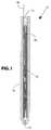
- FIG. 1is a cross-sectional view of a Micro Blade of the current invention at approximately 4 ⁇ scale;
- FIG. 2shows a side view of the Micro Blade of FIG. 1 at approximately 2 ⁇ scale
- FIG. 3Ashows a fragmentary cross-section of a circuit assembly fabricated on a copper substrate, that can be folded to form a system-in-package inside a Micro Blade;
- FIG. 3Bis an expanded cross-sectional view of region B of FIG. 3A , including details of the flip chip connectors;
- FIG. 4is a top view of a system-in-package fabricated on a copper wafer, prior to folding;
- FIG. 5shows a fragmentary cross-section of a cable aligned with a circuit assembly, just prior to physical attachment
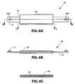
- FIG. 6Ais a schematic top view of a hermetic cable of the current invention.
- FIG. 6Bis a cross-section shown as BB in FIG. 6A ;
- FIG. 6Cis a cross-section shown as CC in FIG. 6A ;
- FIG. 7is a cross-sectional view of a water-cooled system of the current invention.
- FIG. 1illustrates Micro Blade 10 of the current invention, at a scale of approximately 4 ⁇ .
- Micro Blade 10can be of any size, but preferably has a thin form factor for ease of cooling the active circuits inside.
- Copper jacket 11is soldered, welded, or brazed at crimped edges 12 to form a hermetic package.
- Inside the copper jacketis an electronic assembly that is preferably a folded system in package (SIP) 13 including IC chips 14 .
- SIPsystem in package
- Semi-hermetic seal 15may be formed using an epoxy adhesive or a potting compound, as is known in the art.
- Cable 16connects to electronic assembly 13 using a direct attachment (like flip chip), as will be further described. Cable 16 also includes a section that is hermetic, as will be further described.
- FIG. 2is a side view of Micro Blade 10 , showing cable 16 .
- Cable 16typically carries power and high speed signals, as will be further described. Although any width and height are covered under the current invention, W 21 and H 22 are both 45 mm in the preferred embodiment.
- Pressureis applied to the copper sheets of hermetic jacket 11 to assure intimate contact with the circuit assembly inside, while the edges 23 are crimped together. Mating surfaces at the crimped edges are coated with solder paste, or a dry film of solder alloy is laminated between them. Heat and pressure are applied to melt the solder and make a watertight seal.
- FIG. 3Ais a cross-sectional view of a fragment of a circuit assembly 13 A. After fabrication, testing, and any necessary rework, assembly 13 A will be folded to make circuit assembly 13 of FIG. 1 , as will be further described.
- Assembly 13 Aincludes foldable circuit board 31 formed on a copper foil substrate 32 .
- Interconnection circuit 33is preferably fabricated using build up dielectric and conducting layers, as is known in the art. In the preferred embodiment it includes dual damascene copper and dielectric structures that implement transmission lines having a characteristic impedance. The dual damascene structures may be fabricated using a combination of imprinting, electroplating, and chemical mechanical polishing (CMP). Further details of these processes are described in co-pending application, Ser. No. 10/783,921 which is incorporated herein by reference.
- FIG. 3Bis an expanded view of region B of FIG. 3A . It shows a fragment of IC chip 34 having copper spring bumps 35 attached at input/output pads 36 .
- the copper spring bumps 35are inserted into wells 37 containing solder paste that has been heated to form melted solder 38 in the wells.
- the solder in each wellcaptures the end of a copper spring bump as shown, providing a strong mechanical connection and a low-resistance electrical connection.
- This flip chip connectoris labeled 39 in FIG. 3B , and is a good stress reliever in all three dimensions. Such mechanical compliance is desirable for relaxing shear stresses caused by un-matched thermal expansion of IC chips versus circuit boards during temperature excursions.
- Interconnection circuit 33is shown built up on copper substrate 32 , and includes a special assembly layer 40 in which the wells 37 are formed in a dielectric material 41 .
- the walls 42 of the wellsare coated with titanium/copper to provide a solder-wetting surface having good adhesion to dielectric material 41 .
- Dielectric material 41is preferably benzo-cyclo-butene (BCB).
- Flip chip connector 39is shown connecting between an input/output pad 36 on IC chip 34 and a copper trace 43 in interconnection circuit 33 .
- the minimum pitch 44 of flip chip connectors 39is preferably around 80 ⁇ m.
- FIG. 4shows a complete layout for electronic assembly 13 A of FIG. 3A .
- Assembly 13 Ais built on copper foil substrate 32 of FIG. 3A .
- substrate 32may have the same shape and thickness as a silicon wafer. In this case the preferred wafer diameter is 150 mm; however, the wafer can be of any size.
- Interconnection circuit 33 of FIG. 3has been fabricated on copper substrate 32 , with clear areas surrounding alignment targets 50 .
- the set of chips in assembly 13 Ais a chipset that implements a 4 -way server in this example, including 4 processor chips 51 , arrays of memory chips 52 , a test chip 53 , integrated passives 54 , and power distribution devices 55 .
- An area 56is shown for attaching cable 16 of FIG. 1 .
- Assembly 13 Ais tested and any defective chips are replaced.
- Test chip 53 and cable 16are used during testing, employing methods described in co-pending application Ser. No. 10/448,611 incorporated herein by reference.
- a back grinding and lapping procedureis preferably employed to reduce the thickness of all of the chips to approximately 100 microns.
- Copper substrate 32may also be thinned using a grinding/lapping procedure, and the wings 57 of assembly 13 A are folded at fold lines 58 to form electronic assembly 13 of FIG. 1 . More details about the folding and the associated system-in-package are described in co-pending application Ser. No. 10/783,163, incorporated herein by reference.
- FIG. 5illustrates in cross-section the situation just prior to bonding cable 16 of FIG. 1 to foldable circuit board 31 of FIG. 3A using flip chip connectors 39 described in reference to FIG. 3B .
- the attachment procedureis similar to that used for attaching an IC chip like 34 of FIG. 3A .
- a flip chip bonding machine employing split beam opticsis used, having an alignment accuracy of approximately ⁇ 1 micron.
- Copper spring bumps 35are shown aligned to wells 37 containing solder paste 60 that has been deposited in the wells using a squeegee.
- Copper substrate 32 of foldable circuit board 31 and copper substrate 61 of cable 16are preferably connected to ground (GND).
- offset coplanar striplinesare implemented in interconnection circuit 62 of cable 16 , providing a preferred characteristic impedance of 50 ohms.
- the preferred pitch between flip chip connectorsis around 80 microns, as discussed in reference to FIG. 3B . Having a preferred height of approximately 100 ⁇ m, the flip chip connectors have an inductance of approximately 0.1 nH, supporting signaling at multi-gigahertz rates between the Micro Blade and external devices.
- FIG. 6Ashows hermetic cable 65 including cable 16 of FIG. 1 .
- Cable 16has arrays 66 a and 66 b of copper spring elements as described in FIG. 3B .
- Array 66 aconnects to the electronic assembly or SIP inside Micro Blade 10 of FIG. 1
- array 66 btypically connects to a back plane, to be further described.
- a copper sheath 67encloses a center portion of cable 16 as shown, and is crimped at the edges 68 .
- FIG. 6Billustrates section BB of FIG. 6A .
- Copper spring elements 35 of array 66 aare shown.
- Copper sheath 67is preferably fabricated from sheets of copper foil approximately 600 microns thick.
- FIG. 6Cillustrates section CC of FIG.
- hermetic cable 65can be used to traverse a damp or steam-laden path of cable 16 , as will be further described; each end will preferably be dry, where the flip chip connections are made.
- FIG. 7shows a water-cooled electronic system 80 of the current invention in cross-section.
- System 80includes a tank 81 having a lid 82 .
- Tank 81is filled with water 83 to a controlled level 84 .
- An array of Micro Blade elements 10is inserted in tank 80 as shown.
- Micro Blade elementshave a preferred form factor, any hermetic sub-assembly can be similarly immersed for cooling. Partial immersion is preferred as shown, wherein a hermetic jacket protects on all sides against water intrusion.
- a water seal 85is provided for tank 81 as shown, preferably consisting of potting material.
- Back plane printed circuit board 86is shown in a dry environment; this board may be a conventional laminate board constructed from glass fibers and epoxy, or it may be constructed on a copper substrate as shown in FIG. 3A ; in either case it preferably includes wells filled with solder for accepting copper spring elements 66 b of FIG. 6A at the end of cable 16 .
- Circuit board 86may also be a motherboard for integrating electronic activity among all of the Micro Blades or sub-assemblies. Circuit board 86 preferably has slots 87 through which the Micro Blade cables pass. Section 88 of cable 16 of FIG. 1 passes through the potting material of water seal 85 . Such potting materials are not totally impervious to moisture, and this is why the seal is only “semi-hermetic”.
- solder bumpsmay replace copper spring elements at the ends of cable 16 ; they may connect to wells filled with solder, or to corresponding lands on circuit board 86 .
- a further alternativeis to provide pin-and-socket connectors at this end of the cable attachment.
- the outer surfaces of the hermetic jackets 11 of FIG. 1may be desirable to plate the outer surfaces of the hermetic jackets 11 of FIG. 1 with a thin layer of nickel followed by a thin layer of gold, as is known in the art.
- the water 83 in tank 80is preferably circulated through a cooling system (not shown), as is known in the art.
- Water entry ports 90 and exit ports 91are shown. Since water has a specific heat of 4.186 Joules per gram per degree Centigrade, a flow rate of 20 liters per minute will provide over 62 kilowatts of cooling if the water temperature rises by 45° C.
- the Micro Bladesare thermally well coupled to the coolant, since the water is circulating in contact with the jacket surfaces.
- a typical desired maximum junction temperature for the electronic circuits contained inside of a Micro Bladeis 85° C. and a typical temperature for the chilled water is 15° C.
- a thermal resistance ⁇ JC from junction to case of less than 0.05° C./Wis achievable for a Micro Blade of the current invention, as well as heat dissipation exceeding 5 watts per square millimeter of the Micro Blade jacket.
- a preferred maintenance philosophyincludes monitoring the health of the Micro Blades and adding isolation circuits to each; defective ones are switched out of operation without adversely affecting the remaining good units.
- stacks of water-cooled systems 80may be provided. Their total compute and switching power will depend on the total number of Micro Blades in service. This is preferably managed by adding or subtracting systems 80 to meet the peak demand over the long term.
Landscapes
- Engineering & Computer Science (AREA)
- Microelectronics & Electronic Packaging (AREA)
- Physics & Mathematics (AREA)
- Condensed Matter Physics & Semiconductors (AREA)
- General Physics & Mathematics (AREA)
- Computer Hardware Design (AREA)
- Power Engineering (AREA)
- Chemical & Material Sciences (AREA)
- Materials Engineering (AREA)
- Cooling Or The Like Of Semiconductors Or Solid State Devices (AREA)
Abstract
Description
- This application claims priority to Provisional Application Ser. No. 60/569,076 filed May 7, 2004 and to Provisional Application Ser. No. 60/570,199 filed May 11, 2004.
- This invention relates to microelectronic packaging, and more particularly to a blade-shaped component containing a miniaturized electronic assembly (Micro Blade).
- Blade components have a characteristic form factor; they have a thickness dimension substantially smaller that their height and width. This provides a convenient packaging arrangement for a large system, wherein multiple blades can be inserted in slots in a chassis, each blade providing a standalone capability, and each blade replaceable if problems develop.
- Advanced packaging technology may be applied to reduce the dimensions of such a blade assembly. However, dissipating the heat generated in such a miniaturized version is difficult. It is helpful to make the blade as thin as possible. This provides short paths for the heat to escape from the integrated circuit chips inside to an external heat sink. In this manner, and employing advanced cooling methods, a Micro Blade assembly can effectively handle the approximately 500 watts of power associated with a high-end 4-way server. The Micro Blade package typically occupies less than 1% of the volume of a conventional blade device that is fabricated using packaged devices mounted on printed circuit boards. This type of result provides motivation for the Micro Blade form factor.
- An example blade server is the HS40 manufactured by International Business Machines; it is 2.3 inches thick, 9.7 inches high, and 17.6 inches wide. The HS40 can be inserted into a chassis having 16 slots for similarly shaped blade components. The components may have different functions such as processor modules, or switch modules for high data rate communications to or from other components.
- The HS40 includes up to 4 Xeon processors. Because these processors each generate up to 85 watts of heat during operation, they are provided with large and bulky finned aluminum heat sinks; and forced air passes over the fins to cool the processors. These heat sinks occupy approximately 40% of the HS40 blade volume. The total blade electronics requires 480 watts of cooling when four 3 GHz processors are installed. The HS40 also includes a power supply board, a controller board, and memory provided within serial in-line packages; it weighs 15.4 pounds and occupies 393 cubic inches.
- The current invention implements the functions of a board or a blade in a micro-sized version. This micro-sized version preferably has a small thickness dimension and is referred to herein as a Micro Blade. The Micro Blade concept can be applied to a broad class of electronic components, including printed circuit boards, subsystems, system-in-package (SIP), and complete systems. It can be of any size. However, for the purpose of illustration, a particular size is described; this particular size resulting from shrinking the example HS40 device using advanced packaging techniques.
- The Micro Blade version implements the same functions as the HS40 except for some minor differences in power distribution. The size of the preferred embodiment is 45×45×3.2 mm, with a corresponding weight of approximately 0.1 pounds. The corresponding volume is 0.4 cubic inches. Its thinness contributes to effective cooling.
- The Micro Blade embodiment described herein is designed to use the same integrated circuit (IC) chips as the system it replaces. Consequently, it must dissipate the same amount of power, 480 watts in the case of the HS40 server example. In the preferred embodiment, this is achieved using a folded system-in-package (SIP) built on a copper foil substrate; copper comprises approximately 78% of the SIP volume, providing good heat transfer characteristics for cooling. By wrapping the SIP in a hermetic copper jacket it becomes a Micro Blade; a miniaturized stand-alone unit that can be connected to outside elements using a cable. It is mechanically rugged and also thermally rugged; “thermally rugged” means that it can effectively distribute localized hot spots and can also withstand brief surges in overall heat generation. It is preferably cooled in water or other liquid coolant, although air cooling is also a viable option by adding finned elements and forced air, as is known in the art. Yet another option is to provide heat pipes that carry heat produced in the copper jackets to remote radiators where it is dissipated using large area surfaces.
- The foregoing and other objects of the invention will be more clearly understood from the accompanying drawings and description of the invention:
FIG. 1 is a cross-sectional view of a Micro Blade of the current invention at approximately 4× scale;FIG. 2 shows a side view of the Micro Blade ofFIG. 1 at approximately 2× scale;FIG. 3A shows a fragmentary cross-section of a circuit assembly fabricated on a copper substrate, that can be folded to form a system-in-package inside a Micro Blade;FIG. 3B is an expanded cross-sectional view of region B ofFIG. 3A , including details of the flip chip connectors;FIG. 4 is a top view of a system-in-package fabricated on a copper wafer, prior to folding;FIG. 5 shows a fragmentary cross-section of a cable aligned with a circuit assembly, just prior to physical attachment;FIG. 6A is a schematic top view of a hermetic cable of the current invention;FIG. 6B is a cross-section shown as BB inFIG. 6A ;FIG. 6C is a cross-section shown as CC inFIG. 6A ; andFIG. 7 is a cross-sectional view of a water-cooled system of the current invention.- The cross-section of
FIG. 1 illustrates MicroBlade 10 of the current invention, at a scale of approximately 4×. Micro Blade10 can be of any size, but preferably has a thin form factor for ease of cooling the active circuits inside.Copper jacket 11 is soldered, welded, or brazed at crimpededges 12 to form a hermetic package. Inside the copper jacket is an electronic assembly that is preferably a folded system in package (SIP)13 includingIC chips 14. At the top ofMicro Blade 10 is asemi-hermetic seal 15 that also provides a strain relief forcable 16.Semi-hermetic seal 15 may be formed using an epoxy adhesive or a potting compound, as is known in the art.Cable 16 connects toelectronic assembly 13 using a direct attachment (like flip chip), as will be further described.Cable 16 also includes a section that is hermetic, as will be further described. FIG. 2 is a side view ofMicro Blade 10, showingcable 16.Cable 16 typically carries power and high speed signals, as will be further described. Although any width and height are covered under the current invention,W 21 andH 22 are both 45 mm in the preferred embodiment. Pressure is applied to the copper sheets ofhermetic jacket 11 to assure intimate contact with the circuit assembly inside, while theedges 23 are crimped together. Mating surfaces at the crimped edges are coated with solder paste, or a dry film of solder alloy is laminated between them. Heat and pressure are applied to melt the solder and make a watertight seal.FIG. 3A is a cross-sectional view of a fragment of acircuit assembly 13A. After fabrication, testing, and any necessary rework,assembly 13A will be folded to makecircuit assembly 13 ofFIG. 1 , as will be further described.Assembly 13A includesfoldable circuit board 31 formed on acopper foil substrate 32.Interconnection circuit 33 is preferably fabricated using build up dielectric and conducting layers, as is known in the art. In the preferred embodiment it includes dual damascene copper and dielectric structures that implement transmission lines having a characteristic impedance. The dual damascene structures may be fabricated using a combination of imprinting, electroplating, and chemical mechanical polishing (CMP). Further details of these processes are described in co-pending application, Ser. No. 10/783,921 which is incorporated herein by reference.FIG. 3B is an expanded view of region B ofFIG. 3A . It shows a fragment ofIC chip 34 having copper spring bumps35 attached at input/output pads 36. The copper spring bumps35 are inserted intowells 37 containing solder paste that has been heated to form meltedsolder 38 in the wells. The solder in each well captures the end of a copper spring bump as shown, providing a strong mechanical connection and a low-resistance electrical connection. This flip chip connector is labeled39 inFIG. 3B , and is a good stress reliever in all three dimensions. Such mechanical compliance is desirable for relaxing shear stresses caused by un-matched thermal expansion of IC chips versus circuit boards during temperature excursions. Vertical compliance of the spring elements is provided by a bend inspring element 35 as shown; this is additionally useful for accommodating imperfections in the components and in the assembly process. Co-pending application Ser. No. 11/015,213 describes the flip chip connectors in more detail, including methods for manufacture and assembly, and is incorporated herein by reference.Interconnection circuit 33 is shown built up oncopper substrate 32, and includes aspecial assembly layer 40 in which thewells 37 are formed in adielectric material 41. Thewalls 42 of the wells are coated with titanium/copper to provide a solder-wetting surface having good adhesion todielectric material 41.Dielectric material 41 is preferably benzo-cyclo-butene (BCB).Flip chip connector 39 is shown connecting between an input/output pad 36 onIC chip 34 and acopper trace 43 ininterconnection circuit 33. Theminimum pitch 44 offlip chip connectors 39 is preferably around 80 μm.FIG. 4 shows a complete layout forelectronic assembly 13A ofFIG. 3A .Assembly 13A is built oncopper foil substrate 32 ofFIG. 3A . For manufacturing convenience,substrate 32 may have the same shape and thickness as a silicon wafer. In this case the preferred wafer diameter is 150 mm; however, the wafer can be of any size.Interconnection circuit 33 ofFIG. 3 has been fabricated oncopper substrate 32, with clear areas surrounding alignment targets50. The set of chips inassembly 13A is a chipset that implements a4-way server in this example, including4processor chips 51, arrays ofmemory chips 52, atest chip 53,integrated passives 54, andpower distribution devices 55. Anarea 56 is shown for attachingcable 16 ofFIG. 1 .Assembly 13A is tested and any defective chips are replaced.Test chip 53 andcable 16 are used during testing, employing methods described in co-pending application Ser. No. 10/448,611 incorporated herein by reference. A back grinding and lapping procedure is preferably employed to reduce the thickness of all of the chips to approximately 100 microns.Copper substrate 32 may also be thinned using a grinding/lapping procedure, and thewings 57 ofassembly 13A are folded atfold lines 58 to formelectronic assembly 13 ofFIG. 1 . More details about the folding and the associated system-in-package are described in co-pending application Ser. No. 10/783,163, incorporated herein by reference.FIG. 5 illustrates in cross-section the situation just prior tobonding cable 16 ofFIG. 1 tofoldable circuit board 31 ofFIG. 3A usingflip chip connectors 39 described in reference toFIG. 3B . The attachment procedure is similar to that used for attaching an IC chip like34 ofFIG. 3A . A flip chip bonding machine employing split beam optics is used, having an alignment accuracy of approximately ±1 micron. Copper spring bumps35 are shown aligned towells 37 containingsolder paste 60 that has been deposited in the wells using a squeegee.Copper substrate 32 offoldable circuit board 31 andcopper substrate 61 ofcable 16 are preferably connected to ground (GND). For high-speed signals, offset coplanar striplines are implemented ininterconnection circuit 62 ofcable 16, providing a preferred characteristic impedance of 50 ohms. The preferred pitch between flip chip connectors is around 80 microns, as discussed in reference toFIG. 3B . Having a preferred height of approximately 100 μm, the flip chip connectors have an inductance of approximately 0.1 nH, supporting signaling at multi-gigahertz rates between the Micro Blade and external devices.FIG. 6A showshermetic cable 65 includingcable 16 ofFIG. 1 .Cable 16 hasarrays FIG. 3B .Array 66aconnects to the electronic assembly or SIP insideMicro Blade 10 ofFIG. 1 , andarray 66btypically connects to a back plane, to be further described. Acopper sheath 67 encloses a center portion ofcable 16 as shown, and is crimped at theedges 68.FIG. 6B illustrates section BB ofFIG. 6A .Copper spring elements 35 ofarray 66aare shown.Copper sheath 67 is preferably fabricated from sheets of copper foil approximately 600 microns thick.FIG. 6C illustrates section CC ofFIG. 6A , and shows that the seam incopper sheath 67 is hermetically sealed, preferably usingsolder 69. The center hermetic portion ofhermetic cable 65 can be used to traverse a damp or steam-laden path ofcable 16, as will be further described; each end will preferably be dry, where the flip chip connections are made.FIG. 7 shows a water-cooledelectronic system 80 of the current invention in cross-section.System 80 includes atank 81 having alid 82.Tank 81 is filled withwater 83 to a controlledlevel 84. An array ofMicro Blade elements 10 is inserted intank 80 as shown. Although Micro Blade elements have a preferred form factor, any hermetic sub-assembly can be similarly immersed for cooling. Partial immersion is preferred as shown, wherein a hermetic jacket protects on all sides against water intrusion. Awater seal 85 is provided fortank 81 as shown, preferably consisting of potting material. Back plane printedcircuit board 86 is shown in a dry environment; this board may be a conventional laminate board constructed from glass fibers and epoxy, or it may be constructed on a copper substrate as shown inFIG. 3A ; in either case it preferably includes wells filled with solder for acceptingcopper spring elements 66bofFIG. 6A at the end ofcable 16.Circuit board 86 may also be a motherboard for integrating electronic activity among all of the Micro Blades or sub-assemblies.Circuit board 86 preferably hasslots 87 through which the Micro Blade cables pass.Section 88 ofcable 16 ofFIG. 1 passes through the potting material ofwater seal 85. Such potting materials are not totally impervious to moisture, and this is why the seal is only “semi-hermetic”. Residual moisture will likely cause a reliability problem with copper conductors on a cable passing through such a potting material; eventually the metallic conductors will corrode. This is the motivation for creating acable 16 having a center section that is fully hermetic, as described in reference toFIG. 6A . The center hermetic section of the cable protects the cable conductors from residual moisture, either in pottingmaterial 15 ofFIG. 1 ormaterial 85 ofFIG. 7 .Connections 89 betweenMicro Blade cables 16 ofFIG. 1 andback plane 86 are preferably constructed as flip chip connections, as described in reference toFIG. 5 . Other types of flip chip connectors may also be used. For example, solder bumps may replace copper spring elements at the ends ofcable 16; they may connect to wells filled with solder, or to corresponding lands oncircuit board 86. A further alternative is to provide pin-and-socket connectors at this end of the cable attachment.- For corrosion protection, it may be desirable to plate the outer surfaces of the
hermetic jackets 11 ofFIG. 1 with a thin layer of nickel followed by a thin layer of gold, as is known in the art. - The
water 83 intank 80 is preferably circulated through a cooling system (not shown), as is known in the art.Water entry ports 90 andexit ports 91 are shown. Since water has a specific heat of 4.186 Joules per gram per degree Centigrade, a flow rate of 20 liters per minute will provide over 62 kilowatts of cooling if the water temperature rises by 45° C. The Micro Blades are thermally well coupled to the coolant, since the water is circulating in contact with the jacket surfaces. A typical desired maximum junction temperature for the electronic circuits contained inside of a Micro Blade is 85° C. and a typical temperature for the chilled water is 15° C. A thermal resistance θJCfrom junction to case of less than 0.05° C./W is achievable for a Micro Blade of the current invention, as well as heat dissipation exceeding 5 watts per square millimeter of the Micro Blade jacket. - Maintenance of
Micro Blades 10 in water-cooledsystem 80 is difficult; the Micro Blades are semi-permanently attached usingpotting material 85. Accordingly, a preferred maintenance philosophy includes monitoring the health of the Micro Blades and adding isolation circuits to each; defective ones are switched out of operation without adversely affecting the remaining good units. In a data center for example, stacks of water-cooledsystems 80 may be provided. Their total compute and switching power will depend on the total number of Micro Blades in service. This is preferably managed by adding or subtractingsystems 80 to meet the peak demand over the long term.
Claims (14)
1. A micro blade comprising:
a miniaturized electronic assembly;
a jacket enclosing said electronic assembly, said jacket comprising thermally conductive members that are joined using hermetic seams;
an adhesive compound sealing an open end of said jacket; and,
a cable attached to said electronic assembly that passes through said adhesive compound in said open end for making an external connection to said electronic assembly.
2. The micro blade ofclaim 1 wherein said electronic assembly comprises a circuit board having attached components.
3. The micro blade ofclaim 2 wherein said circuit board is flexible.
4. The micro blade ofclaim 3 wherein said circuit board is folded.
5. The micro blade ofclaim 4 wherein said folded circuit board employs a copper substrate.
6. The micro blade ofclaim 2 wherein said attached components include said attached cable plus integrated circuit chips.
7. The micro blade ofclaim 6 wherein said components are attached used flip chip attachments.
8. The micro blade ofclaim 7 wherein each of said flip chip attachments comprises an array of bumps inserted into a corresponding array of wells filled with solder.
9. The micro blade ofclaim 8 wherein said bumps are copper spring elements.
10. The micro blade ofclaim 1 wherein said thermally conductive members are sheets of copper, or an alloy of copper.
11. The micro blade ofclaim 1 wherein said attached cable includes a middle section that is hermetically sealed.
12. A cable with a hermetic center section comprising:
a cable substrate;
build-up layers including dielectric layers and conductive materials forming traces;
terminals at each end of said cable that connect with said traces; and,
a sealed conductive sheath enclosing said hermetic center section of said cable.
13. The cable ofclaim 12 wherein said conductive sheath is fabricated from a sheet of metal and said sheet is hermetically joined at crimped edges of said sheath.
14. The cable ofclaim 13 wherein said hermetic seal includes solder.
Priority Applications (1)
| Application Number | Priority Date | Filing Date | Title |
|---|---|---|---|
| US11/101,935US20050255722A1 (en) | 2004-05-07 | 2005-04-08 | Micro blade assembly |
Applications Claiming Priority (3)
| Application Number | Priority Date | Filing Date | Title |
|---|---|---|---|
| US56907604P | 2004-05-07 | 2004-05-07 | |
| US57019904P | 2004-05-11 | 2004-05-11 | |
| US11/101,935US20050255722A1 (en) | 2004-05-07 | 2005-04-08 | Micro blade assembly |
Publications (1)
| Publication Number | Publication Date |
|---|---|
| US20050255722A1true US20050255722A1 (en) | 2005-11-17 |
Family
ID=35309995
Family Applications (1)
| Application Number | Title | Priority Date | Filing Date |
|---|---|---|---|
| US11/101,935AbandonedUS20050255722A1 (en) | 2004-05-07 | 2005-04-08 | Micro blade assembly |
Country Status (1)
| Country | Link |
|---|---|
| US (1) | US20050255722A1 (en) |
Cited By (11)
| Publication number | Priority date | Publication date | Assignee | Title |
|---|---|---|---|---|
| US20040176924A1 (en)* | 2003-03-07 | 2004-09-09 | Salmon Peter C. | Apparatus and method for testing electronic systems |
| US20050040513A1 (en)* | 2003-08-20 | 2005-02-24 | Salmon Peter C. | Copper-faced modules, imprinted copper circuits, and their application to supercomputers |
| US20050184376A1 (en)* | 2004-02-19 | 2005-08-25 | Salmon Peter C. | System in package |
| US20060036831A1 (en)* | 2004-08-10 | 2006-02-16 | Matsushita Electric Industrial Co., Ltd. | Multiprocessor |
| US20060079009A1 (en)* | 2004-10-12 | 2006-04-13 | Salmon Peter C | Fine-pitch electronic socket for temporary or permanent attachments |
| US20060131728A1 (en)* | 2004-12-16 | 2006-06-22 | Salmon Peter C | Repairable three-dimensional semiconductor subsystem |
| US7586747B2 (en) | 2005-08-01 | 2009-09-08 | Salmon Technologies, Llc. | Scalable subsystem architecture having integrated cooling channels |
| US20130000117A1 (en)* | 2011-06-30 | 2013-01-03 | Rajashree Baskaran | Liquid metal interconnects |
| US20130258594A1 (en)* | 2012-03-28 | 2013-10-03 | Abb Research Ltd | Heat exchanger for traction converters |
| US9496154B2 (en) | 2014-09-16 | 2016-11-15 | Invensas Corporation | Use of underfill tape in microelectronic components, and microelectronic components with cavities coupled to through-substrate vias |
| US20250087540A1 (en)* | 2023-09-07 | 2025-03-13 | Peter C. Salmon | Hermetic microelectronic module using a sheath |
Citations (91)
| Publication number | Priority date | Publication date | Assignee | Title |
|---|---|---|---|---|
| US2060970A (en)* | 1936-01-13 | 1936-11-17 | Gen Motors Corp | Spacer |
| US4455654A (en)* | 1981-06-05 | 1984-06-19 | John Fluke Mfg. Co., Inc. | Test apparatus for electronic assemblies employing a microprocessor |
| US4748495A (en)* | 1985-08-08 | 1988-05-31 | Dypax Systems Corporation | High density multi-chip interconnection and cooling package |
| US4862322A (en)* | 1988-05-02 | 1989-08-29 | Bickford Harry R | Double electronic device structure having beam leads solderlessly bonded between contact locations on each device and projecting outwardly from therebetween |
| US4912844A (en)* | 1988-08-10 | 1990-04-03 | Dimensional Circuits Corporation | Methods of producing printed circuit boards |
| US5001548A (en)* | 1989-03-13 | 1991-03-19 | Coriolis Corporation | Multi-chip module cooling |
| US5070297A (en)* | 1990-06-04 | 1991-12-03 | Texas Instruments Incorporated | Full wafer integrated circuit testing device |
| US5159529A (en)* | 1991-05-15 | 1992-10-27 | International Business Machines Corporation | Composite liquid cooled plate for electronic equipment |
| US5162974A (en)* | 1991-04-15 | 1992-11-10 | Unisys Corporation | Heat sink assembly for cooling electronic components |
| US5214250A (en)* | 1991-09-19 | 1993-05-25 | International Business Machines Corporation | Method of reworking circuit panels, and circuit panels reworked thereby |
| US5239200A (en)* | 1991-08-21 | 1993-08-24 | International Business Machines Corporation | Apparatus for cooling integrated circuit chips |
| US5239448A (en)* | 1991-10-28 | 1993-08-24 | International Business Machines Corporation | Formulation of multichip modules |
| US5267867A (en)* | 1992-09-11 | 1993-12-07 | Digital Equipment Corporation | Package for multiple removable integrated circuits |
| US5281151A (en)* | 1991-07-05 | 1994-01-25 | Hitachi, Ltd. | Semiconductor chip carrier, module having same chip carrier mounted therein, and electronic device incorporating same module |
| US5291064A (en)* | 1991-04-16 | 1994-03-01 | Nec Corporation | Package structure for semiconductor device having a flexible wiring circuit member spaced from the package casing |
| US5305184A (en)* | 1992-12-16 | 1994-04-19 | Ibm Corporation | Method and apparatus for immersion cooling or an electronic board |
| US5334279A (en)* | 1993-04-08 | 1994-08-02 | Gregoire George D | Method and apparatus for making printed circuit boards |
| US5367593A (en)* | 1993-09-03 | 1994-11-22 | Motorola, Inc. | Optical/electrical connector and method of fabrication |
| US5461327A (en)* | 1992-08-31 | 1995-10-24 | Tokyo Electron Limited | Probe apparatus |
| US5510758A (en)* | 1993-04-07 | 1996-04-23 | Matsushita Electric Industrial Co., Ltd. | Multilayer microstrip wiring board with a semiconductor device mounted thereon via bumps |
| US5579574A (en)* | 1994-01-28 | 1996-12-03 | Molex Incorporated | Method of fabricating flat flexible circuits |
| US5627406A (en)* | 1994-12-22 | 1997-05-06 | Pace; Benedict G. | Inverted chip bonded module with high packaging efficiency |
| US5635767A (en)* | 1995-06-02 | 1997-06-03 | Motorola, Inc. | Semiconductor device having built-in high frequency bypass capacitor |
| US5640051A (en)* | 1993-12-13 | 1997-06-17 | Matsushita Electric Industrial Co., Ltd. | Chip package, a chip carrier, a terminal electrode for a circuit substrate and a chip package-mounted complex |
| US5701666A (en)* | 1994-08-31 | 1997-12-30 | Motorola, Inc. | Method for manufacturing a stimulus wafer for use in a wafer-to-wafer testing system to test integrated circuits located on a product wafer |
| US5774475A (en)* | 1996-12-05 | 1998-06-30 | National Semiconductor Corporation | Testing scheme that re-uses original stimulus for testing circuitry embedded within a larger circuit |
| US5797771A (en)* | 1996-08-16 | 1998-08-25 | U.S. Robotics Mobile Communication Corp. | Cable connector |
| US5800060A (en)* | 1992-08-19 | 1998-09-01 | Geraberger Thermometer Werk Gmbh | Clinical thermometer |
| US5847936A (en)* | 1997-06-20 | 1998-12-08 | Sun Microsystems, Inc. | Optimized routing scheme for an integrated circuit/printed circuit board |
| US5900738A (en)* | 1993-11-16 | 1999-05-04 | Formfactor, Inc. | Contact structure device for interconnections, interposer, semiconductor assembly and package using the same and method |
| US5972152A (en)* | 1997-05-16 | 1999-10-26 | Micron Communications, Inc. | Methods of fixturing flexible circuit substrates and a processing carrier, processing a flexible circuit and processing a flexible circuit substrate relative to a processing carrier |
| US5998738A (en)* | 1996-08-30 | 1999-12-07 | Motorola Inc. | Electronic control module |
| US6005198A (en)* | 1997-10-07 | 1999-12-21 | Dimensional Circuits Corporation | Wiring board constructions and methods of making same |
| US6103554A (en)* | 1998-01-08 | 2000-08-15 | Samsung Electronics, Co., Ltd. | Method for packaging integrated circuits with elastomer chip carriers |
| US6121676A (en)* | 1996-12-13 | 2000-09-19 | Tessera, Inc. | Stacked microelectronic assembly and method therefor |
| US6138348A (en)* | 1989-12-18 | 2000-10-31 | Polymer Flip Chip Corporation | Method of forming electrically conductive polymer interconnects on electrical substrates |
| US6174804B1 (en)* | 1998-05-26 | 2001-01-16 | United Microelectronics Corp. | Dual damascene manufacturing process |
| US6208511B1 (en)* | 1998-12-31 | 2001-03-27 | Lucent Technologies, Inc. | Arrangement for enclosing a fluid and method of manufacturing a fluid retaining enclosure |
| US6210229B1 (en)* | 1998-12-31 | 2001-04-03 | Hon Hai Precision Ind. Co., Ltd. | Shielded cable connector assembly |
| US6225688B1 (en)* | 1997-12-11 | 2001-05-01 | Tessera, Inc. | Stacked microelectronic assembly and method therefor |
| US6246010B1 (en)* | 1998-11-25 | 2001-06-12 | 3M Innovative Properties Company | High density electronic package |
| US6304447B1 (en)* | 1998-12-31 | 2001-10-16 | Lucent Technologies, Inc. | Arrangement for cooling an electrical assembly |
| US6310484B1 (en)* | 1996-04-01 | 2001-10-30 | Micron Technology, Inc. | Semiconductor test interconnect with variable flexure contacts |
| US20020030975A1 (en)* | 2000-06-28 | 2002-03-14 | Moon Ow Chee | Packaged microelectronic die assemblies and methods of manufacture |
| US6372549B2 (en)* | 2000-04-24 | 2002-04-16 | Nec Corporation | Semiconductor package and semiconductor package fabrication method |
| US6392301B1 (en)* | 1999-10-22 | 2002-05-21 | Intel Corporation | Chip package and method |
| US6441476B1 (en)* | 2000-10-18 | 2002-08-27 | Seiko Epson Corporation | Flexible tape carrier with external terminals formed on interposers |
| US20020121689A1 (en)* | 2000-03-09 | 2002-09-05 | Nec Corporation | Flip chip type semiconductor device and method for manufacturing the same |
| US6476885B1 (en)* | 1999-07-19 | 2002-11-05 | National Semiconductor Corporation | Stress-free socketed optical display package with die non-rigidly attached to containment structure |
| US6515870B1 (en)* | 2000-11-27 | 2003-02-04 | Intel Corporation | Package integrated faraday cage to reduce electromagnetic emissions from an integrated circuit |
| US6528891B2 (en)* | 1998-12-17 | 2003-03-04 | Charles Wen Chyang Lin | Bumpless flip chip assembly with solder via |
| US20030106004A1 (en)* | 2001-12-04 | 2003-06-05 | Intellitech Corporation | Method and apparatus for embedded built-in self-test (BIST) of electronic circuits and systems |
| US6587345B2 (en)* | 2001-11-09 | 2003-07-01 | International Business Machines Corporation | Electronic device substrate assembly with impermeable barrier and method of making |
| US20030168725A1 (en)* | 1996-12-13 | 2003-09-11 | Tessera, Inc. | Methods of making microelectronic assemblies including folded substrates |
| US6631344B1 (en)* | 1999-03-26 | 2003-10-07 | Synopsys, Inc. | Method and system for performing deterministic analysis and speculative analysis for more efficient automatic test pattern generation |
| US6683377B1 (en)* | 2000-05-30 | 2004-01-27 | Amkor Technology, Inc. | Multi-stacked memory package |
| US6690845B1 (en)* | 1998-10-09 | 2004-02-10 | Fujitsu Limited | Three-dimensional opto-electronic modules with electrical and optical interconnections and methods for making |
| US6722893B2 (en)* | 2002-03-18 | 2004-04-20 | High Connection Density, Inc. | Test and burn-in connector |
| US6749587B2 (en)* | 2001-02-22 | 2004-06-15 | Insulet Corporation | Modular infusion device and method |
| US6763880B1 (en)* | 2003-06-26 | 2004-07-20 | Evserv Tech Corporation | Liquid cooled radiation module for servers |
| US20040148121A1 (en)* | 2003-01-17 | 2004-07-29 | Texas Instruments Incorporated | On-chip test mechanism for transceiver power amplifier and oscillator frequency |
| US6784554B2 (en)* | 2001-12-26 | 2004-08-31 | Hitachi, Ltd. | Semiconductor device and manufacturing method thereof |
| US20040176924A1 (en)* | 2003-03-07 | 2004-09-09 | Salmon Peter C. | Apparatus and method for testing electronic systems |
| US6845477B2 (en)* | 2000-05-29 | 2005-01-18 | Renesas Technology Corp. | Semiconductor test device for conducting an operation test in parallel on many chips in a wafer test and semiconductor test method |
| US20050040513A1 (en)* | 2003-08-20 | 2005-02-24 | Salmon Peter C. | Copper-faced modules, imprinted copper circuits, and their application to supercomputers |
| US6881609B2 (en)* | 2001-09-07 | 2005-04-19 | Peter C. Salmon | Component connections using bumps and wells |
| US6891732B2 (en)* | 2001-09-25 | 2005-05-10 | Shinko Electric Industries Co., Ltd. | Multilayer circuit board and semiconductor device using the same |
| US6927471B2 (en)* | 2001-09-07 | 2005-08-09 | Peter C. Salmon | Electronic system modules and method of fabrication |
| US20050184376A1 (en)* | 2004-02-19 | 2005-08-25 | Salmon Peter C. | System in package |
| US6938678B1 (en)* | 2000-06-23 | 2005-09-06 | Lucent Technologies Inc. | Arrangement for liquid cooling an electrical assembly using assisted flow |
| US6942493B2 (en)* | 2001-11-13 | 2005-09-13 | Unitechno Inc. | Connector structure for connecting electronic parts |
| US6955063B2 (en)* | 2003-06-14 | 2005-10-18 | Nanomist Systems, Llc | Cooling of electronics and high density power dissipation systems by fine-mist flooding |
| US6956284B2 (en)* | 2001-10-26 | 2005-10-18 | Staktek Group L.P. | Integrated circuit stacking system and method |
| US6956285B2 (en)* | 2003-01-15 | 2005-10-18 | Sun Microsystems, Inc. | EMI grounding pins for CPU/ASIC chips |
| US6973717B2 (en)* | 1998-07-14 | 2005-12-13 | Infineon Technologies Ag | Method for producing a semiconductor device in chip format |
| US6990176B2 (en)* | 2003-10-30 | 2006-01-24 | General Electric Company | Methods and apparatus for tileable sensor array |
| US7009412B2 (en)* | 1999-05-27 | 2006-03-07 | Nanonexus, Inc. | Massively parallel interface for electronic circuit |
| US20060077638A1 (en)* | 2004-10-12 | 2006-04-13 | Salmon Peter C | Adaptive interface using flexible fingers |
| US7040383B2 (en)* | 2001-08-16 | 2006-05-09 | Nec Corporation | Telecommunication device including a housing having improved heat conductivity |
| US20060131728A1 (en)* | 2004-12-16 | 2006-06-22 | Salmon Peter C | Repairable three-dimensional semiconductor subsystem |
| US20060145715A1 (en)* | 2005-01-06 | 2006-07-06 | Salmon Peter C | Wafer level test head |
| US7078926B2 (en)* | 1993-11-16 | 2006-07-18 | Formfactor, Inc. | Wafer-level burn-in and test |
| US20060209512A1 (en)* | 2005-03-17 | 2006-09-21 | Fujitsu Limited | Heat receiving member, heat receiving device and electronic equipment |
| US20070007983A1 (en)* | 2005-01-06 | 2007-01-11 | Salmon Peter C | Semiconductor wafer tester |
| US7163830B2 (en)* | 2004-10-12 | 2007-01-16 | Salmon Peter C | Method for temporarily engaging electronic component for test |
| US20070025079A1 (en)* | 2005-08-01 | 2007-02-01 | Salmon Peter C | Scalable subsystem architecture having integrated cooling channels |
| US20070023904A1 (en)* | 2005-08-01 | 2007-02-01 | Salmon Peter C | Electro-optic interconnection apparatus and method |
| US20070023889A1 (en)* | 2005-08-01 | 2007-02-01 | Salmon Peter C | Copper substrate with feedthroughs and interconnection circuits |
| US20070023923A1 (en)* | 2005-08-01 | 2007-02-01 | Salmon Peter C | Flip chip interface including a mixed array of heat bumps and signal bumps |
| US7224856B2 (en)* | 2001-10-23 | 2007-05-29 | Digital Optics Corporation | Wafer based optical chassis and associated methods |
| US7254024B2 (en)* | 2004-05-11 | 2007-08-07 | Salmon Peter C | Cooling apparatus and method |
- 2005
- 2005-04-08USUS11/101,935patent/US20050255722A1/ennot_activeAbandoned
Patent Citations (95)
| Publication number | Priority date | Publication date | Assignee | Title |
|---|---|---|---|---|
| US2060970A (en)* | 1936-01-13 | 1936-11-17 | Gen Motors Corp | Spacer |
| US4455654A (en)* | 1981-06-05 | 1984-06-19 | John Fluke Mfg. Co., Inc. | Test apparatus for electronic assemblies employing a microprocessor |
| US4455654B1 (en)* | 1981-06-05 | 1991-04-30 | Test apparatus for electronic assemblies employing a microprocessor | |
| US4748495A (en)* | 1985-08-08 | 1988-05-31 | Dypax Systems Corporation | High density multi-chip interconnection and cooling package |
| US4862322A (en)* | 1988-05-02 | 1989-08-29 | Bickford Harry R | Double electronic device structure having beam leads solderlessly bonded between contact locations on each device and projecting outwardly from therebetween |
| US4912844A (en)* | 1988-08-10 | 1990-04-03 | Dimensional Circuits Corporation | Methods of producing printed circuit boards |
| US5001548A (en)* | 1989-03-13 | 1991-03-19 | Coriolis Corporation | Multi-chip module cooling |
| US6138348A (en)* | 1989-12-18 | 2000-10-31 | Polymer Flip Chip Corporation | Method of forming electrically conductive polymer interconnects on electrical substrates |
| US5070297A (en)* | 1990-06-04 | 1991-12-03 | Texas Instruments Incorporated | Full wafer integrated circuit testing device |
| US5162974A (en)* | 1991-04-15 | 1992-11-10 | Unisys Corporation | Heat sink assembly for cooling electronic components |
| US5291064A (en)* | 1991-04-16 | 1994-03-01 | Nec Corporation | Package structure for semiconductor device having a flexible wiring circuit member spaced from the package casing |
| US5159529A (en)* | 1991-05-15 | 1992-10-27 | International Business Machines Corporation | Composite liquid cooled plate for electronic equipment |
| US5281151A (en)* | 1991-07-05 | 1994-01-25 | Hitachi, Ltd. | Semiconductor chip carrier, module having same chip carrier mounted therein, and electronic device incorporating same module |
| US5239200A (en)* | 1991-08-21 | 1993-08-24 | International Business Machines Corporation | Apparatus for cooling integrated circuit chips |
| US5214250A (en)* | 1991-09-19 | 1993-05-25 | International Business Machines Corporation | Method of reworking circuit panels, and circuit panels reworked thereby |
| US5239448A (en)* | 1991-10-28 | 1993-08-24 | International Business Machines Corporation | Formulation of multichip modules |
| US5800060A (en)* | 1992-08-19 | 1998-09-01 | Geraberger Thermometer Werk Gmbh | Clinical thermometer |
| US5461327A (en)* | 1992-08-31 | 1995-10-24 | Tokyo Electron Limited | Probe apparatus |
| US5267867A (en)* | 1992-09-11 | 1993-12-07 | Digital Equipment Corporation | Package for multiple removable integrated circuits |
| US5305184A (en)* | 1992-12-16 | 1994-04-19 | Ibm Corporation | Method and apparatus for immersion cooling or an electronic board |
| US5510758A (en)* | 1993-04-07 | 1996-04-23 | Matsushita Electric Industrial Co., Ltd. | Multilayer microstrip wiring board with a semiconductor device mounted thereon via bumps |
| US5390412A (en)* | 1993-04-08 | 1995-02-21 | Gregoire; George D. | Method for making printed circuit boards |
| US5334279A (en)* | 1993-04-08 | 1994-08-02 | Gregoire George D | Method and apparatus for making printed circuit boards |
| US5451722A (en)* | 1993-04-08 | 1995-09-19 | Gregoire; George D. | Printed circuit board with metallized grooves |
| US5367593A (en)* | 1993-09-03 | 1994-11-22 | Motorola, Inc. | Optical/electrical connector and method of fabrication |
| US5900738A (en)* | 1993-11-16 | 1999-05-04 | Formfactor, Inc. | Contact structure device for interconnections, interposer, semiconductor assembly and package using the same and method |
| US7078926B2 (en)* | 1993-11-16 | 2006-07-18 | Formfactor, Inc. | Wafer-level burn-in and test |
| US5640051A (en)* | 1993-12-13 | 1997-06-17 | Matsushita Electric Industrial Co., Ltd. | Chip package, a chip carrier, a terminal electrode for a circuit substrate and a chip package-mounted complex |
| US5579574A (en)* | 1994-01-28 | 1996-12-03 | Molex Incorporated | Method of fabricating flat flexible circuits |
| US5701666A (en)* | 1994-08-31 | 1997-12-30 | Motorola, Inc. | Method for manufacturing a stimulus wafer for use in a wafer-to-wafer testing system to test integrated circuits located on a product wafer |
| US5627406A (en)* | 1994-12-22 | 1997-05-06 | Pace; Benedict G. | Inverted chip bonded module with high packaging efficiency |
| US5635767A (en)* | 1995-06-02 | 1997-06-03 | Motorola, Inc. | Semiconductor device having built-in high frequency bypass capacitor |
| US6310484B1 (en)* | 1996-04-01 | 2001-10-30 | Micron Technology, Inc. | Semiconductor test interconnect with variable flexure contacts |
| US5797771A (en)* | 1996-08-16 | 1998-08-25 | U.S. Robotics Mobile Communication Corp. | Cable connector |
| US5998738A (en)* | 1996-08-30 | 1999-12-07 | Motorola Inc. | Electronic control module |
| US5774475A (en)* | 1996-12-05 | 1998-06-30 | National Semiconductor Corporation | Testing scheme that re-uses original stimulus for testing circuitry embedded within a larger circuit |
| US20030168725A1 (en)* | 1996-12-13 | 2003-09-11 | Tessera, Inc. | Methods of making microelectronic assemblies including folded substrates |
| US6121676A (en)* | 1996-12-13 | 2000-09-19 | Tessera, Inc. | Stacked microelectronic assembly and method therefor |
| US5972152A (en)* | 1997-05-16 | 1999-10-26 | Micron Communications, Inc. | Methods of fixturing flexible circuit substrates and a processing carrier, processing a flexible circuit and processing a flexible circuit substrate relative to a processing carrier |
| US5847936A (en)* | 1997-06-20 | 1998-12-08 | Sun Microsystems, Inc. | Optimized routing scheme for an integrated circuit/printed circuit board |
| US6005198A (en)* | 1997-10-07 | 1999-12-21 | Dimensional Circuits Corporation | Wiring board constructions and methods of making same |
| US6460247B1 (en)* | 1997-10-07 | 2002-10-08 | Dimensional Circuits Corp. | Wiring board constructions and methods of making same |
| US6225688B1 (en)* | 1997-12-11 | 2001-05-01 | Tessera, Inc. | Stacked microelectronic assembly and method therefor |
| US6103554A (en)* | 1998-01-08 | 2000-08-15 | Samsung Electronics, Co., Ltd. | Method for packaging integrated circuits with elastomer chip carriers |
| US6174804B1 (en)* | 1998-05-26 | 2001-01-16 | United Microelectronics Corp. | Dual damascene manufacturing process |
| US6973717B2 (en)* | 1998-07-14 | 2005-12-13 | Infineon Technologies Ag | Method for producing a semiconductor device in chip format |
| US6690845B1 (en)* | 1998-10-09 | 2004-02-10 | Fujitsu Limited | Three-dimensional opto-electronic modules with electrical and optical interconnections and methods for making |
| US6246010B1 (en)* | 1998-11-25 | 2001-06-12 | 3M Innovative Properties Company | High density electronic package |
| US6528891B2 (en)* | 1998-12-17 | 2003-03-04 | Charles Wen Chyang Lin | Bumpless flip chip assembly with solder via |
| US6304447B1 (en)* | 1998-12-31 | 2001-10-16 | Lucent Technologies, Inc. | Arrangement for cooling an electrical assembly |
| US6210229B1 (en)* | 1998-12-31 | 2001-04-03 | Hon Hai Precision Ind. Co., Ltd. | Shielded cable connector assembly |
| US6208511B1 (en)* | 1998-12-31 | 2001-03-27 | Lucent Technologies, Inc. | Arrangement for enclosing a fluid and method of manufacturing a fluid retaining enclosure |
| US6631344B1 (en)* | 1999-03-26 | 2003-10-07 | Synopsys, Inc. | Method and system for performing deterministic analysis and speculative analysis for more efficient automatic test pattern generation |
| US7009412B2 (en)* | 1999-05-27 | 2006-03-07 | Nanonexus, Inc. | Massively parallel interface for electronic circuit |
| US6476885B1 (en)* | 1999-07-19 | 2002-11-05 | National Semiconductor Corporation | Stress-free socketed optical display package with die non-rigidly attached to containment structure |
| US6392301B1 (en)* | 1999-10-22 | 2002-05-21 | Intel Corporation | Chip package and method |
| US20020121689A1 (en)* | 2000-03-09 | 2002-09-05 | Nec Corporation | Flip chip type semiconductor device and method for manufacturing the same |
| US6372549B2 (en)* | 2000-04-24 | 2002-04-16 | Nec Corporation | Semiconductor package and semiconductor package fabrication method |
| US6845477B2 (en)* | 2000-05-29 | 2005-01-18 | Renesas Technology Corp. | Semiconductor test device for conducting an operation test in parallel on many chips in a wafer test and semiconductor test method |
| US6683377B1 (en)* | 2000-05-30 | 2004-01-27 | Amkor Technology, Inc. | Multi-stacked memory package |
| US6938678B1 (en)* | 2000-06-23 | 2005-09-06 | Lucent Technologies Inc. | Arrangement for liquid cooling an electrical assembly using assisted flow |
| US20020030975A1 (en)* | 2000-06-28 | 2002-03-14 | Moon Ow Chee | Packaged microelectronic die assemblies and methods of manufacture |
| US6441476B1 (en)* | 2000-10-18 | 2002-08-27 | Seiko Epson Corporation | Flexible tape carrier with external terminals formed on interposers |
| US6515870B1 (en)* | 2000-11-27 | 2003-02-04 | Intel Corporation | Package integrated faraday cage to reduce electromagnetic emissions from an integrated circuit |
| US6749587B2 (en)* | 2001-02-22 | 2004-06-15 | Insulet Corporation | Modular infusion device and method |
| US7040383B2 (en)* | 2001-08-16 | 2006-05-09 | Nec Corporation | Telecommunication device including a housing having improved heat conductivity |
| US6881609B2 (en)* | 2001-09-07 | 2005-04-19 | Peter C. Salmon | Component connections using bumps and wells |
| US6927471B2 (en)* | 2001-09-07 | 2005-08-09 | Peter C. Salmon | Electronic system modules and method of fabrication |
| US6891732B2 (en)* | 2001-09-25 | 2005-05-10 | Shinko Electric Industries Co., Ltd. | Multilayer circuit board and semiconductor device using the same |
| US7224856B2 (en)* | 2001-10-23 | 2007-05-29 | Digital Optics Corporation | Wafer based optical chassis and associated methods |
| US6956284B2 (en)* | 2001-10-26 | 2005-10-18 | Staktek Group L.P. | Integrated circuit stacking system and method |
| US6587345B2 (en)* | 2001-11-09 | 2003-07-01 | International Business Machines Corporation | Electronic device substrate assembly with impermeable barrier and method of making |
| US6942493B2 (en)* | 2001-11-13 | 2005-09-13 | Unitechno Inc. | Connector structure for connecting electronic parts |
| US20030106004A1 (en)* | 2001-12-04 | 2003-06-05 | Intellitech Corporation | Method and apparatus for embedded built-in self-test (BIST) of electronic circuits and systems |
| US6784554B2 (en)* | 2001-12-26 | 2004-08-31 | Hitachi, Ltd. | Semiconductor device and manufacturing method thereof |
| US6722893B2 (en)* | 2002-03-18 | 2004-04-20 | High Connection Density, Inc. | Test and burn-in connector |
| US6956285B2 (en)* | 2003-01-15 | 2005-10-18 | Sun Microsystems, Inc. | EMI grounding pins for CPU/ASIC chips |
| US20040148121A1 (en)* | 2003-01-17 | 2004-07-29 | Texas Instruments Incorporated | On-chip test mechanism for transceiver power amplifier and oscillator frequency |
| US20040176924A1 (en)* | 2003-03-07 | 2004-09-09 | Salmon Peter C. | Apparatus and method for testing electronic systems |
| US6955063B2 (en)* | 2003-06-14 | 2005-10-18 | Nanomist Systems, Llc | Cooling of electronics and high density power dissipation systems by fine-mist flooding |
| US6763880B1 (en)* | 2003-06-26 | 2004-07-20 | Evserv Tech Corporation | Liquid cooled radiation module for servers |
| US20050040513A1 (en)* | 2003-08-20 | 2005-02-24 | Salmon Peter C. | Copper-faced modules, imprinted copper circuits, and their application to supercomputers |
| US6990176B2 (en)* | 2003-10-30 | 2006-01-24 | General Electric Company | Methods and apparatus for tileable sensor array |
| US20050184376A1 (en)* | 2004-02-19 | 2005-08-25 | Salmon Peter C. | System in package |
| US7254024B2 (en)* | 2004-05-11 | 2007-08-07 | Salmon Peter C | Cooling apparatus and method |
| US20060077638A1 (en)* | 2004-10-12 | 2006-04-13 | Salmon Peter C | Adaptive interface using flexible fingers |
| US7163830B2 (en)* | 2004-10-12 | 2007-01-16 | Salmon Peter C | Method for temporarily engaging electronic component for test |
| US20060131728A1 (en)* | 2004-12-16 | 2006-06-22 | Salmon Peter C | Repairable three-dimensional semiconductor subsystem |
| US20070007983A1 (en)* | 2005-01-06 | 2007-01-11 | Salmon Peter C | Semiconductor wafer tester |
| US20060145715A1 (en)* | 2005-01-06 | 2006-07-06 | Salmon Peter C | Wafer level test head |
| US20060209512A1 (en)* | 2005-03-17 | 2006-09-21 | Fujitsu Limited | Heat receiving member, heat receiving device and electronic equipment |
| US20070025079A1 (en)* | 2005-08-01 | 2007-02-01 | Salmon Peter C | Scalable subsystem architecture having integrated cooling channels |
| US20070023904A1 (en)* | 2005-08-01 | 2007-02-01 | Salmon Peter C | Electro-optic interconnection apparatus and method |
| US20070023889A1 (en)* | 2005-08-01 | 2007-02-01 | Salmon Peter C | Copper substrate with feedthroughs and interconnection circuits |
| US20070023923A1 (en)* | 2005-08-01 | 2007-02-01 | Salmon Peter C | Flip chip interface including a mixed array of heat bumps and signal bumps |
Cited By (19)
| Publication number | Priority date | Publication date | Assignee | Title |
|---|---|---|---|---|
| US7505862B2 (en) | 2003-03-07 | 2009-03-17 | Salmon Technologies, Llc | Apparatus and method for testing electronic systems |
| US20040176924A1 (en)* | 2003-03-07 | 2004-09-09 | Salmon Peter C. | Apparatus and method for testing electronic systems |
| US20090192753A1 (en)* | 2003-03-07 | 2009-07-30 | Salmon Peter C | Apparatus and method for testing electronic systems |
| US20050040513A1 (en)* | 2003-08-20 | 2005-02-24 | Salmon Peter C. | Copper-faced modules, imprinted copper circuits, and their application to supercomputers |
| US7408258B2 (en) | 2003-08-20 | 2008-08-05 | Salmon Technologies, Llc | Interconnection circuit and electronic module utilizing same |
| US20050184376A1 (en)* | 2004-02-19 | 2005-08-25 | Salmon Peter C. | System in package |
| US20060036831A1 (en)* | 2004-08-10 | 2006-02-16 | Matsushita Electric Industrial Co., Ltd. | Multiprocessor |
| US7689129B2 (en)* | 2004-08-10 | 2010-03-30 | Panasonic Corporation | System-in-package optical transceiver in optical communication with a plurality of other system-in-package optical transceivers via an optical transmission line |
| US20060079009A1 (en)* | 2004-10-12 | 2006-04-13 | Salmon Peter C | Fine-pitch electronic socket for temporary or permanent attachments |
| US7163830B2 (en)* | 2004-10-12 | 2007-01-16 | Salmon Peter C | Method for temporarily engaging electronic component for test |
| US7427809B2 (en) | 2004-12-16 | 2008-09-23 | Salmon Technologies, Llc | Repairable three-dimensional semiconductor subsystem |
| US20060131728A1 (en)* | 2004-12-16 | 2006-06-22 | Salmon Peter C | Repairable three-dimensional semiconductor subsystem |
| US7586747B2 (en) | 2005-08-01 | 2009-09-08 | Salmon Technologies, Llc. | Scalable subsystem architecture having integrated cooling channels |
| US20130000117A1 (en)* | 2011-06-30 | 2013-01-03 | Rajashree Baskaran | Liquid metal interconnects |
| US9835648B2 (en)* | 2011-06-30 | 2017-12-05 | Intel Corporation | Liquid metal interconnects |
| US20130258594A1 (en)* | 2012-03-28 | 2013-10-03 | Abb Research Ltd | Heat exchanger for traction converters |
| US9097467B2 (en)* | 2012-03-28 | 2015-08-04 | Abb Research Ltd | Heat exchanger for traction converters |
| US9496154B2 (en) | 2014-09-16 | 2016-11-15 | Invensas Corporation | Use of underfill tape in microelectronic components, and microelectronic components with cavities coupled to through-substrate vias |
| US20250087540A1 (en)* | 2023-09-07 | 2025-03-13 | Peter C. Salmon | Hermetic microelectronic module using a sheath |
Similar Documents
| Publication | Publication Date | Title |
|---|---|---|
| US7254024B2 (en) | Cooling apparatus and method | |
| US8362607B2 (en) | Integrated circuit package including a thermally and electrically conductive package lid | |
| JP2561793B2 (en) | Direct chip attach module | |
| US6396136B2 (en) | Ball grid package with multiple power/ground planes | |
| CN101292360B (en) | Integrated circuit mounting for thermal stress relief usable in multi-chip modules | |
| US5016138A (en) | Three dimensional integrated circuit package | |
| US6339254B1 (en) | Stacked flip-chip integrated circuit assemblage | |
| US6489687B1 (en) | Semiconductor device and method of manufacturing the same, manufacturing device, circuit board, and electronic equipment | |
| US6451626B1 (en) | Three-dimensional stacked semiconductor package | |
| US4034468A (en) | Method for making conduction-cooled circuit package | |
| US5307240A (en) | Chiplid, multichip semiconductor package design concept | |
| JP3726318B2 (en) | Chip size package, manufacturing method thereof, and second level packaging | |
| US20110085304A1 (en) | Thermal management device comprising thermally conductive heat spreader with electrically isolated through-hole vias | |
| US20050189636A1 (en) | Packaging substrates for integrated circuits and soldering methods | |
| US6583513B1 (en) | Integrated circuit package with an IC chip and pads that dissipate heat away from the chip | |
| JP2004312034A (en) | Circuit assembly and method of connecting radiator to integrated circuit device | |
| KR20080031119A (en) | Semiconductor devices | |
| US20050255722A1 (en) | Micro blade assembly | |
| CN101425510A (en) | Laminated packaging structure of semiconductor element and method thereof | |
| JPH11191603A (en) | Semiconductor integrated circuit and its manufacture | |
| US20090121340A1 (en) | Fully testable surface mount die package configured for two-sided cooling | |
| KR100675030B1 (en) | Integrated circuit package | |
| AU629711B2 (en) | Hybrid module electronics package | |
| US20070063334A1 (en) | Semiconductor device | |
| JP2865496B2 (en) | Multi-chip module |
Legal Events
| Date | Code | Title | Description |
|---|---|---|---|
| AS | Assignment | Owner name:PETER C. SALMON, LLC, A CALIFORNIA LIMITED LIABILI Free format text:ASSIGNMENT OF ASSIGNORS INTEREST;ASSIGNOR:SALMON, PETER C.;REEL/FRAME:019031/0849 Effective date:20070313 | |
| AS | Assignment | Owner name:SALMON TECHNOLOGIES, LLC, CALIFORNIA Free format text:ASSIGNMENT OF ASSIGNORS INTEREST;ASSIGNOR:PETER C. SALMON, LLC;REEL/FRAME:019789/0839 Effective date:20070905 | |
| STCB | Information on status: application discontinuation | Free format text:ABANDONED -- FAILURE TO RESPOND TO AN OFFICE ACTION |