US20050255647A1 - Vertical NROM having a storage density of 1 bit per 1F2 - Google Patents
Vertical NROM having a storage density of 1 bit per 1F2Download PDFInfo
- Publication number
- US20050255647A1 US20050255647A1US11/122,764US12276405AUS2005255647A1US 20050255647 A1US20050255647 A1US 20050255647A1US 12276405 AUS12276405 AUS 12276405AUS 2005255647 A1US2005255647 A1US 2005255647A1
- Authority
- US
- United States
- Prior art keywords
- source
- region
- drain region
- gate
- mosfet
- Prior art date
- Legal status (The legal status is an assumption and is not a legal conclusion. Google has not performed a legal analysis and makes no representation as to the accuracy of the status listed.)
- Granted
Links
- 238000003860storageMethods0.000titleclaimsdescription78
- 239000012212insulatorSubstances0.000claimsabstractdescription96
- 230000015654memoryEffects0.000claimsabstractdescription76
- 239000000758substrateSubstances0.000claimsabstractdescription45
- 239000002131composite materialSubstances0.000claimsabstractdescription21
- 239000004065semiconductorSubstances0.000claimsabstractdescription20
- 238000002347injectionMethods0.000claimsabstractdescription19
- 239000007924injectionSubstances0.000claimsabstractdescription19
- 230000005669field effectEffects0.000claimsabstractdescription9
- 229910044991metal oxideInorganic materials0.000claimsabstractdescription9
- 150000004706metal oxidesChemical class0.000claimsabstractdescription9
- 229910052710siliconInorganic materials0.000claimsdescription24
- 239000010703siliconSubstances0.000claimsdescription24
- XUIMIQQOPSSXEZ-UHFFFAOYSA-NSiliconChemical compound[Si]XUIMIQQOPSSXEZ-UHFFFAOYSA-N0.000claimsdescription22
- 239000002784hot electronSubstances0.000claimsdescription19
- 238000000034methodMethods0.000claimsdescription17
- 239000000463materialSubstances0.000claimsdescription6
- 239000010936titaniumSubstances0.000claimsdescription6
- RTAQQCXQSZGOHL-UHFFFAOYSA-NTitaniumChemical compound[Ti]RTAQQCXQSZGOHL-UHFFFAOYSA-N0.000claimsdescription4
- 229910052735hafniumInorganic materials0.000claimsdescription4
- VBJZVLUMGGDVMO-UHFFFAOYSA-Nhafnium atomChemical compound[Hf]VBJZVLUMGGDVMO-UHFFFAOYSA-N0.000claimsdescription4
- 229910052746lanthanumInorganic materials0.000claimsdescription4
- FZLIPJUXYLNCLC-UHFFFAOYSA-Nlanthanum atomChemical compound[La]FZLIPJUXYLNCLC-UHFFFAOYSA-N0.000claimsdescription4
- 229910052715tantalumInorganic materials0.000claimsdescription4
- GUVRBAGPIYLISA-UHFFFAOYSA-Ntantalum atomChemical compound[Ta]GUVRBAGPIYLISA-UHFFFAOYSA-N0.000claimsdescription4
- 229910052719titaniumInorganic materials0.000claimsdescription4
- 230000004044responseEffects0.000claims3
- 230000008878couplingEffects0.000claims1
- 238000010168coupling processMethods0.000claims1
- 238000005859coupling reactionMethods0.000claims1
- 239000010410layerSubstances0.000description30
- VYPSYNLAJGMNEJ-UHFFFAOYSA-NSilicium dioxideChemical compoundO=[Si]=OVYPSYNLAJGMNEJ-UHFFFAOYSA-N0.000description24
- TWNQGVIAIRXVLR-UHFFFAOYSA-Noxo(oxoalumanyloxy)alumaneChemical compoundO=[Al]O[Al]=OTWNQGVIAIRXVLR-UHFFFAOYSA-N0.000description16
- 230000005540biological transmissionEffects0.000description13
- 230000008859changeEffects0.000description12
- 238000005516engineering processMethods0.000description12
- 229910052814silicon oxideInorganic materials0.000description10
- 238000010586diagramMethods0.000description8
- 238000003491arrayMethods0.000description7
- 239000000377silicon dioxideSubstances0.000description7
- 229910052581Si3N4Inorganic materials0.000description6
- 230000015556catabolic processEffects0.000description6
- 239000002800charge carrierSubstances0.000description6
- 238000006731degradation reactionMethods0.000description6
- 230000000694effectsEffects0.000description6
- HQVNEWCFYHHQES-UHFFFAOYSA-Nsilicon nitrideChemical compoundN12[Si]34N5[Si]62N3[Si]51N64HQVNEWCFYHHQES-UHFFFAOYSA-N0.000description6
- 238000012986modificationMethods0.000description5
- 230000004048modificationEffects0.000description5
- 239000003990capacitorSubstances0.000description4
- 239000002105nanoparticleSubstances0.000description4
- 150000004767nitridesChemical class0.000description4
- 235000012239silicon dioxideNutrition0.000description4
- 230000005641tunnelingEffects0.000description4
- 230000006399behaviorEffects0.000description3
- 230000008901benefitEffects0.000description3
- 238000012937correctionMethods0.000description3
- 238000012545processingMethods0.000description3
- 235000012431wafersNutrition0.000description3
- 238000009279wet oxidation reactionMethods0.000description3
- 238000004891communicationMethods0.000description2
- 239000004020conductorSubstances0.000description2
- 238000013500data storageMethods0.000description2
- 238000013461designMethods0.000description2
- 230000006870functionEffects0.000description2
- MRELNEQAGSRDBK-UHFFFAOYSA-Nlanthanum(3+);oxygen(2-)Chemical compound[O-2].[O-2].[O-2].[La+3].[La+3]MRELNEQAGSRDBK-UHFFFAOYSA-N0.000description2
- 230000014759maintenance of locationEffects0.000description2
- 238000004519manufacturing processMethods0.000description2
- 230000007246mechanismEffects0.000description2
- 230000008569processEffects0.000description2
- HBMJWWWQQXIZIP-UHFFFAOYSA-Nsilicon carbideChemical compound[Si+]#[C-]HBMJWWWQQXIZIP-UHFFFAOYSA-N0.000description2
- 229910010271silicon carbideInorganic materials0.000description2
- 239000002356single layerSubstances0.000description2
- 102100037807GATOR complex protein MIOSHuman genes0.000description1
- 101000950705Homo sapiens GATOR complex protein MIOSProteins0.000description1
- 101150022794IDS2 geneProteins0.000description1
- 101100491259Oryza sativa subsp. japonica AP2-2 geneProteins0.000description1
- 230000003213activating effectEffects0.000description1
- 230000003321amplificationEffects0.000description1
- 230000015572biosynthetic processEffects0.000description1
- 238000012512characterization methodMethods0.000description1
- 230000005516deep trapEffects0.000description1
- 230000007547defectEffects0.000description1
- 238000009826distributionMethods0.000description1
- 238000010893electron trapMethods0.000description1
- 229910000449hafnium oxideInorganic materials0.000description1
- WIHZLLGSGQNAGK-UHFFFAOYSA-Nhafnium(4+);oxygen(2-)Chemical compound[O-2].[O-2].[Hf+4]WIHZLLGSGQNAGK-UHFFFAOYSA-N0.000description1
- 229910052751metalInorganic materials0.000description1
- 239000002184metalSubstances0.000description1
- 239000000203mixtureSubstances0.000description1
- 238000003199nucleic acid amplification methodMethods0.000description1
- 238000013386optimize processMethods0.000description1
- 230000003071parasitic effectEffects0.000description1
- 230000002093peripheral effectEffects0.000description1
- 238000004886process controlMethods0.000description1
- 239000000243solutionSubstances0.000description1
- 238000012360testing methodMethods0.000description1
- 238000012546transferMethods0.000description1
- 229910052720vanadiumInorganic materials0.000description1
Images


Classifications
- H—ELECTRICITY
- H10—SEMICONDUCTOR DEVICES; ELECTRIC SOLID-STATE DEVICES NOT OTHERWISE PROVIDED FOR
- H10B—ELECTRONIC MEMORY DEVICES
- H10B12/00—Dynamic random access memory [DRAM] devices
- H—ELECTRICITY
- H10—SEMICONDUCTOR DEVICES; ELECTRIC SOLID-STATE DEVICES NOT OTHERWISE PROVIDED FOR
- H10B—ELECTRONIC MEMORY DEVICES
- H10B43/00—EEPROM devices comprising charge-trapping gate insulators
- H10B43/30—EEPROM devices comprising charge-trapping gate insulators characterised by the memory core region
- G—PHYSICS
- G11—INFORMATION STORAGE
- G11C—STATIC STORES
- G11C16/00—Erasable programmable read-only memories
- G11C16/02—Erasable programmable read-only memories electrically programmable
- G11C16/04—Erasable programmable read-only memories electrically programmable using variable threshold transistors, e.g. FAMOS
- G11C16/0466—Erasable programmable read-only memories electrically programmable using variable threshold transistors, e.g. FAMOS comprising cells with charge storage in an insulating layer, e.g. metal-nitride-oxide-silicon [MNOS], silicon-oxide-nitride-oxide-silicon [SONOS]
- G11C16/0475—Erasable programmable read-only memories electrically programmable using variable threshold transistors, e.g. FAMOS comprising cells with charge storage in an insulating layer, e.g. metal-nitride-oxide-silicon [MNOS], silicon-oxide-nitride-oxide-silicon [SONOS] comprising two or more independent storage sites which store independent data
- H—ELECTRICITY
- H10—SEMICONDUCTOR DEVICES; ELECTRIC SOLID-STATE DEVICES NOT OTHERWISE PROVIDED FOR
- H10B—ELECTRONIC MEMORY DEVICES
- H10B12/00—Dynamic random access memory [DRAM] devices
- H10B12/01—Manufacture or treatment
- H10B12/09—Manufacture or treatment with simultaneous manufacture of the peripheral circuit region and memory cells
- H—ELECTRICITY
- H10—SEMICONDUCTOR DEVICES; ELECTRIC SOLID-STATE DEVICES NOT OTHERWISE PROVIDED FOR
- H10B—ELECTRONIC MEMORY DEVICES
- H10B12/00—Dynamic random access memory [DRAM] devices
- H10B12/50—Peripheral circuit region structures
- H—ELECTRICITY
- H10—SEMICONDUCTOR DEVICES; ELECTRIC SOLID-STATE DEVICES NOT OTHERWISE PROVIDED FOR
- H10B—ELECTRONIC MEMORY DEVICES
- H10B69/00—Erasable-and-programmable ROM [EPROM] devices not provided for in groups H10B41/00 - H10B63/00, e.g. ultraviolet erasable-and-programmable ROM [UVEPROM] devices
- H—ELECTRICITY
- H10—SEMICONDUCTOR DEVICES; ELECTRIC SOLID-STATE DEVICES NOT OTHERWISE PROVIDED FOR
- H10D—INORGANIC ELECTRIC SEMICONDUCTOR DEVICES
- H10D30/00—Field-effect transistors [FET]
- H10D30/01—Manufacture or treatment
- H10D30/021—Manufacture or treatment of FETs having insulated gates [IGFET]
- H10D30/0413—Manufacture or treatment of FETs having insulated gates [IGFET] of FETs having charge-trapping gate insulators, e.g. MNOS transistors
- H—ELECTRICITY
- H10—SEMICONDUCTOR DEVICES; ELECTRIC SOLID-STATE DEVICES NOT OTHERWISE PROVIDED FOR
- H10D—INORGANIC ELECTRIC SEMICONDUCTOR DEVICES
- H10D30/00—Field-effect transistors [FET]
- H10D30/60—Insulated-gate field-effect transistors [IGFET]
- H10D30/69—IGFETs having charge trapping gate insulators, e.g. MNOS transistors
- H10D30/691—IGFETs having charge trapping gate insulators, e.g. MNOS transistors having more than two programming levels
- H—ELECTRICITY
- H10—SEMICONDUCTOR DEVICES; ELECTRIC SOLID-STATE DEVICES NOT OTHERWISE PROVIDED FOR
- H10D—INORGANIC ELECTRIC SEMICONDUCTOR DEVICES
- H10D30/00—Field-effect transistors [FET]
- H10D30/60—Insulated-gate field-effect transistors [IGFET]
- H10D30/69—IGFETs having charge trapping gate insulators, e.g. MNOS transistors
- H10D30/693—Vertical IGFETs having charge trapping gate insulators
- H—ELECTRICITY
- H10—SEMICONDUCTOR DEVICES; ELECTRIC SOLID-STATE DEVICES NOT OTHERWISE PROVIDED FOR
- H10D—INORGANIC ELECTRIC SEMICONDUCTOR DEVICES
- H10D64/00—Electrodes of devices having potential barriers
- H10D64/01—Manufacture or treatment
- H10D64/031—Manufacture or treatment of data-storage electrodes
- H10D64/037—Manufacture or treatment of data-storage electrodes comprising charge-trapping insulators
- B—PERFORMING OPERATIONS; TRANSPORTING
- B82—NANOTECHNOLOGY
- B82Y—SPECIFIC USES OR APPLICATIONS OF NANOSTRUCTURES; MEASUREMENT OR ANALYSIS OF NANOSTRUCTURES; MANUFACTURE OR TREATMENT OF NANOSTRUCTURES
- B82Y10/00—Nanotechnology for information processing, storage or transmission, e.g. quantum computing or single electron logic
Definitions
- the present inventionrelates generally to semiconductor integrated circuits and, more particularly, to vertical NROM having a storage density of one bit for each 1.0 lithographic feature squared (1F 2 ) unit area.
- DRAMdynamic random access memory
- MOSFETmetal oxide semiconductor field effect transistor
- the present inventionencompasses a vertical multiple bit memory cell, comprising a vertical metal oxide semiconductor field effect transistor (MOSFET) that extends horizontally outward from a substrate.
- MOSFETvertical metal oxide semiconductor field effect transistor
- the MOSFEThas a first source/drain region, a second source/drain region, a channel region between the first and the second source/drain regions, and a gate.
- the gateis separated from the channel region by a high dielectric constant gate insulator that can store a first charge in a first storage region and a second charge in a second storage region.
- the gate insulatormay have a composite structure of oxide-nitride-aluminum oxide.
- the trapping layer of the gate insulatorincludes layers of hafnium oxide or lanthanum oxide.
- the vertical memory cellcan be programmed and erased by applying a negative voltage to the substrate. This creates enhanced hot electron injection.
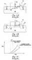
- FIG. 1Ais a block diagram of a metal oxide semiconductor field effect transistor (MOSFET) in a substrate according to the teachings of the prior art.
- MOSFETmetal oxide semiconductor field effect transistor
- FIG. 1Billustrates the MOSFET of FIG. 1A operated in the forward direction showing some degree of device degradation due to electrons being trapped in the gate oxide near the drain region over gradual use.
- FIG. 1Cis a graph showing the square root of the current signal (Ids) taken at the drain region of the conventional MOSFET versus the voltage potential (VGS) established between the gate and the source region.
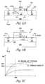
- FIG. 2Ais a diagram of a programmed MOSFET that can be used as a multiple bit cell according to the teachings of the present invention.
- FIG. 2Bis a diagram suitable for explaining the method by which the MOSFET of the multiple bit cell of the present invention can be programmed to achieve the embodiments of the present invention.
- FIG. 2Cis a graph plotting the current signal (Ids) detected at the drain region versus a voltage potential, or drain voltage, (VDS) set up between the drain region and the source region (Ids vs. VDS).
- FIG. 3Aillustrates a vertical NROM 301 having a storage density of one bit per one photolithographic feature squared (1F 2 ) unit area according to the teachings of the present invention.
- FIG. 3Billustrates an electrical equivalent circuit for the vertical NROM device structure shown in FIG. 3A .
- FIG. 4Aillustrates a portion of a memory array 400 according to the teachings of the present invention.
- FIG. 4Billustrates an electrical equivalent circuit 400 for the portion of the memory array shown in FIG. 4A .
- FIGS. 5A-5Billustrates the operation of the novel vertical multiple bit cell formed according to the teachings of the present invention.
- FIG. 6illustrates the operation of a conventional DRAM cell.
- FIG. 7illustrates a memory device according to the teachings of the present invention.
- FIG. 8is a block diagram of an electrical system, or processor-based system, utilizing vertical multiple bit cells constructed in accordance with the present invention.
- wafer and substrate used in the following descriptioninclude any structure having an exposed surface with which to form the integrated circuit (IC) structure of the invention.
- substrateis understood to include semiconductor wafers.
- substrateis also used to refer to semiconductor structures during processing, and may include other layers that have been fabricated thereupon. Both wafer and substrate include doped and undoped semiconductors, epitaxial semiconductor layers supported by a base semiconductor or insulator, as well as other semiconductor structures well known to one skilled in the art.
- conductoris understood to include semiconductors
- insulatoris defined to include any material that is less electrically conductive than the materials referred to as conductors.
- FIG. 1Ais useful in illustrating the conventional operation of a MOSFET such as can be used in a DRAM array.
- FIG. 1Aillustrates the normal hot electron injection and degradation of devices operated in the forward direction. As is explained below, since the electrons are trapped near the drain they are not very effective in changing the device characteristics.
- FIG. 1Ais a block diagram of a metal oxide semiconductor field effect transistor (MOSFET) 101 in a substrate 100 .
- the MOSFET 101includes a source region 102 , a drain region 104 , a channel region 106 in the substrate 100 between the source region 102 and the drain region 104 .
- a gate 108is separated from the channel region 108 by a gate oxide 110 .
- a sourceline 112is coupled to the source region 102 .
- a bitline 114is coupled to the drain region 104 .
- a wordline 116is coupled to the gate 108 .
- a drain to source voltage potential(Vds) is set up between the drain region 104 and the source region 102 .
- a voltage potentialis then applied to the gate 108 via a wordline 116 .
- Vtcharacteristic voltage threshold
- a channel 106forms in the substrate 100 between the drain region 104 and the source region 102 . Formation of the channel 106 permits conduction between the drain region 104 and the source region 102 , and a current signal (Ids) can be detected at the drain region 104 .
- FIG. 1Cillustrates this point.
- FIG. 1Cis a graph showing the square root of the current signal (Ids) taken at the drain region versus the voltage potential (VGS) established between the gate 108 and the source region 102 .
- the change in the slope of the plot of ⁇ square root ⁇ square root over (Ids) ⁇ versus VGSrepresents the change in the charge carrier mobility in the channel 106 .
- ⁇ VTrepresents the minimal change in the MOSFET's threshold voltage resulting from electrons gradually being trapped in the gate oxide 110 near the drain region 104 , under normal operation, due to device degradation. This results in a fixed trapped charge in the gate oxide 110 near the drain region 104 .
- Slope 1represents the charge carrier mobility in the channel 106 for FIG. 1A having no electrons trapped in the gate oxide 110 .
- Slope 2represents the charge mobility in the channel 106 for the conventional MOSFET of FIG. 1B having electrons 117 trapped in the gate oxide 110 near the drain region 104 .
- slope 1 and slope 2 in FIG. 1Cthe electrons 117 trapped in the gate oxide 110 near the drain region 104 of the conventional MOSFET do not significantly change the charge mobility in the channel 106 .
- One componentincludes a threshold voltage shift due to the trapped electrons and a second component includes mobility degradation due to additional scattering of carrier electrons caused by this trapped charge and additional surface states.
- a conventional MOSFETdegrades or is “stressed” over operation in the forward direction, electrons do gradually get injected and become trapped in the gate oxide near the drain. In this portion of the conventional MOSFET there is virtually no channel underneath the gate oxide. Thus the trapped charge modulates the threshold voltage and charge mobility only slightly.
- the inventorshave previously described programmable memory devices and functions based on the reverse stressing of MOSFETs in a conventional CMOS process and technology in order to form programmable address decode and correction. (See generally, L. Forbes, W. P. Noble and E. H. Cloud, “MOSFET technology for programmable address decode and correction,” application Ser. No. 09/383,804). That disclosure, however, did not describe vertical multiple bit cell solutions, but rather address decode and correction issues.
- normal MOSFETscan be programmed by operation in the reverse direction and utilizing avalanche hot electron injection to trap electrons in the gate oxide of the MOSFET.
- the programmed MOSFETis subsequently operated in the forward direction the electrons trapped in the oxide are near the source and cause the channel to have two different threshold voltage regions.
- the novel programmed MOSFETs of the present inventionconduct significantly less current than conventional MOSFETs, particularly at low drain voltages. These electrons will remain trapped in the gate oxide unless negative gate voltages are applied. The electrons will not be removed from the gate oxide when positive or zero gate voltages are applied.
- Erasurecan be accomplished by applying negative gate voltages and/or increasing the temperature with negative gate bias applied to cause the trapped electrons to be re-emitted back into the silicon channel of the MOSFET.
- negative gate voltagesSee generally, L. Forbes, E. Sun, R. Alders and J. Moll, “Field induced re-emission of electrons trapped in SiO2,” IEEE Trans. Electron Device, vol. ED-26, no. 11, pp. 1816-1818 (November 1979); S. S. B. Or, N. Hwang, and L. Forbes, “Tunneling and Thermal emission from a distribution of deep traps in SiO2,” IEEE Trans. on Electron Devices, vol. 40, no. 6, pp. 1100-1103 (June 1993); S. A. Abbas and R. C. Dockerty, “N-channel IGFET design limitations due to hot electron trapping,” IEEE Int. Electron Devices Mtg., Washington D.C., December 1975, pp. 35-38).
- FIGS. 2A-2Care useful in illustrating the present invention in which a much larger change in device characteristics is obtained by programming the device in the reverse direction and subsequently reading the device by operating it in the forward direction.
- FIG. 2Ais a diagram of a programmed MOSFET that can be used as a multiple bit cell according to the teachings of the present invention.
- the multiple bit cell 201includes a MOSFET in a substrate 200 which has a first source/drain region 202 , a second source/drain region 204 , and a channel region 206 between the first and second source/drain regions, 202 and 204 .
- the first source/drain region 202includes a source region 202 for the MOSFET and the second source/drain region 204 includes a drain region 204 for the MOSFET.
- FIG. 2Afurther illustrates a gate 208 separated from the channel region 206 by a gate oxide 210 .
- a first transmission line 212is coupled to the first source/drain region 202 and a second transmission line 214 is coupled to the second source/drain region 204 .
- the first transmission lineincludes a sourceline 212 and the second transmission line includes a bit line 214 .
- the multiple bit cell 201is comprised of a programmed MOSFET.
- This programmed MOSFEThas a charge 217 trapped in the gate oxide 210 adjacent to the first source/drain region 202 such that the channel region 206 has a first voltage threshold region (Vt 1 ) and a second voltage threshold region (Vt 2 ) in the channel 206 .
- the charge 217 trapped in the gate oxide 210 adjacent to the first source/drain region 202includes a trapped electron charge 217 .
- the multiple bit cellcan be programmed to have a charge stored in at least one of a first storage region and a second storage region in the gate insulator 210 and operated with either the first source/drain region 202 or the second source/drain region 204 serving as the source region such that the multiple bit cell 201 will have a first voltage threshold region (Vt 1 ) and a second voltage threshold region (Vt 2 ) and such that the programmed multiple bit cell operates at reduced drain source current.
- Vt 1first voltage threshold region
- Vt 2second voltage threshold region
- FIG. 2Aillustrates the Vt 2 in the channel 206 is adjacent the first source/drain region 202 and that the Vt 1 in the channel 206 is adjacent the second source/drain region 204 .
- Vt 1is adjacent the first source/drain region.
- Vt 2 and Vt 1vary depending on in which direction the multiple bit cell is operated. In this manner multiple bits can be stored on the multiple bit cell 201 .
- FIG. 2Bis a diagram suitable for explaining the method by which the MOSFET of the multiple bit cell 201 of the present invention can be programmed to achieve the embodiments of the present invention.
- the methodincludes programming the MOSFET in a reverse direction.
- Programming the MOSFET in the reverse directionincludes applying a first voltage potential V 1 to a drain region 204 of the MOSFET.
- applying a first voltage potential V 1 to the drain region 204 of the MOSFETincludes grounding the drain region 204 of the MOSFET as shown in FIG. 2B .
- a second voltage potential V 2is applied to a source region 202 of the MOSFET.
- applying a second voltage potential V 2 to the source region 202includes applying a high positive voltage potential (VDD) to the source region 202 of the MOSFET, as shown in FIG. 2B .
- a gate potential VGSis applied to a gate 208 of the MOSFET.
- the gate potential VGSincludes a voltage potential which is less than the second voltage potential V 2 , but which is sufficient to establish conduction in the channel 206 of the MOSFET between the drain region 204 and the source region 202 . As shown in FIG.
- applying the first, second and gate potentials (V 1 , V 2 , and VGS respectively) to the MOSFETcreates a hot electron injection into a gate oxide 210 of the MOSFET adjacent to the source region 202 .
- applying the first, second and gate potentials (V 1 , V 2 , and VGS respectively)provides enough energy to the charge carriers, e.g. electrons, being conducted across the channel 206 that, once the charge carriers are near the source region 202 , a number of the charge carriers get excited into the gate oxide 210 adjacent to the source region 202 .
- the charge carriersbecome trapped.
- the methodis continued by subsequently operating the MOSFET in the forward direction in its programmed state during a read operation.
- the read operationincludes grounding the source region 202 and precharging the drain region a fractional voltage of VDD. If the device is addressed by a wordline coupled to the gate, then its conductivity will be determined by the presence or absence of stored charge in the gate insulator. That is, a gate potential can be applied to the gate 208 by a wordline 216 in an effort to form a conduction channel between the source and the drain regions as done with addressing and reading conventional DRAM cells.
- the conduction channel 206 of the MOSFETwill have a first voltage threshold region (Vt 1 ) adjacent to the drain region 204 and a second voltage threshold region (Vt 2 ) adjacent to the source region 202 , as explained and described in detail in connection with FIG. 2A .
- the Vt 2has a greater voltage threshold than the Vt 1 due to the hot electron injection 217 into a gate oxide 210 of the MOSFET adjacent to the source region 202 .
- a negative substrate biasVsub is applied to the p-type substrate 200 .
- This biasincreases the surface lateral field near a source/drain region 202 or 204 (depending on which direction the cell is operated), thus increasing the number of hot electrons.
- Such a substrate enhanced hot electron injection embodimentwould require a lower drain voltage during programming operations.
- the negative substrate biasis in the range of 0V to ⁇ 3V. Alternate embodiments may use other voltage ranges.
- FIG. 2Cis a graph plotting a current signal (Ids) detected at the second source/drain region 204 versus a voltage potential, or drain voltage, (VDS) set up between the second source/drain region 204 and the first source/drain region 202 (Ids vs. VDS).
- VDSrepresents the voltage potential set up between the drain region 204 and the source region 202 .
- the curve plotted as D 1represents the conduction behavior of a conventional MOSFET which is not programmed according to the teachings of the present invention.
- the curve D 2represents the conduction behavior of the programmed MOSFET, described above in connection with FIG. 2A , according to the teachings of the present invention. As shown in FIG.
- the current signal (IDS 2 ) detected at the second source/drain region 204 for the programmed MOSFET (curve D 2 )is significantly lower than the current signal (IDS 1 ) detected at the second source/drain region 204 for the conventional MOSFET which is not programmed according to the teachings of the present invention.
- the channel 206 in the programmed MOSFET of the present inventionhas two voltage threshold regions and that the voltage threshold, Vt 2 , near the first source/drain region 202 has a higher voltage threshold than Vt 1 near the second source/drain region due to the charge 217 trapped in the gate oxide 217 adjacent to the first source/drain region 202 .
- NROMNonvolatile Memory Cell
- B. Eitan et al.“Characterization of Channel Hot Electron Injection by the Subthreshold Slope of NROM device,” IEEE Electron Device Lett., Vol. 22, No. 11, pp. 556-558, (November 2001); B. Etian et al., “NROM: A novel localized Trapping, 2-Bit Nonvolatile Memory Cell,” IEEE Electron Device Lett., Vol. 21, No. 11, pp. 543-545, (November 2000)).
- Charge trapping in silicon nitride gate insulatorswas the basic mechanism used in MNOS memory devices (see generally, S. Sze, Physics of Semiconductor Devices, Wiley, N.Y., 1981, pp. 504-506), charge trapping in aluminum oxide gates was the mechanism used in MIOS memory devices (see generally, S. Sze, Physics of Semiconductor Devices, Wiley, N.Y., 1981, pp. 504-506), and the present inventors have previously disclosed charge trapping at isolated point defects in gate insulators (see generally, L. Forbes and J. Geusic, “Memory using insulator traps,” U.S. Pat. No. 6,140,181, issued Oct. 31, 2000).
- the present inventiondisclosures programming a MOSFET in a reverse direction to trap charge in a first or a second storage region in a gate insulator adjacent either a first or a second source/drain region.
- the MOSFETcan be programmed and operated in either direction such that the MOSFET has a storage density of 1 bit/1F 2 .
- the MOSFETcan be operated with either the first or the second source/drain region serving as the source such that a charge trapped in the gate insulator in either the first or the second storage region, adjacent to the first or the second source/drain region serving as the source, will provide a reduced drain source current.
- the MOSFET having a storage density of 1 bit/1F 2is based on a modification of DRAM technology.
- Prior art DRAM technologygenerally employs silicon oxide as the gate insulator. Further the emphasis in conventional DRAM devices is placed on trying to minimize charge trapping in the silicon oxide gate insulator. According to the teachings of the present invention, a variety of insulators are used to trap electrons more efficiently than in silicon oxide. That is, in the present invention, the vertical multiple bit memory cell employs charge trapping in gate insulators such as, wet silicon oxide, silicon nitride, silicon oxynitride SON, silicon rich oxide SRO, aluminum oxide Al 2 O 3 . Additionally, composite layers of these insulators such as oxide and silicon nitride, oxide and aluminum oxide, or multiple layers as oxide-nitride-oxide. While the charge trapping efficiency of silicon oxide may be low such is not the case for silicon nitride or composite layers of silicon oxide and nitride.
- FIG. 3Aillustrates a vertical NROM 301 having a storage density of one bit per one photolithographic feature squared (I F 2 ) unit area according to the teachings of the present invention.
- the vertical NROM 301includes a vertical metal oxide semiconductor field effect transistor (MOSFET) 301 extending outwardly from a substrate 300 .
- the MOSFET 301has a first source/drain region 302 that, in this n-channel embodiment, includes a heavily doped (n+) n-type region layered with an n-type doped region.
- the MOSFET 301includes a similarly structured second source/drain region 306 .
- a channel region 305is located in the vertical pillar between the first and the second source/drain regions, 302 and 306 respectively.
- a gate 309is separated from the channel region 305 by a gate insulator 307 as is located alongside of the vertical pillar opposing the channel region 305 .
- the gate insulator 307includes a gate insulator formed of an oxide-nitride-oxide (ONO) composition 307 .
- the gate insulator 307includes a gate insulator selected from the group of silicon dioxide (SiO 2 ) formed by wet oxidation, silicon oxynitride (SON), silicon rich oxide (SRO), and silicon rich aluminum oxide (Al 2 O 3 ).
- the gate insulator 307has a thickness of approximately 10 nanometers (nm).
- the gate insulator 307includes a gate insulator 307 selected from the group of silicon rich aluminum oxide insulators, silicon rich oxides with inclusions of nanoparticles of silicon, silicon oxide insulators with inclusions of nanoparticles of silicon carbide, and silicon oxycarbide insulators.
- the gate insulator 307includes a composite layer selected from the group of an oxide-aluminum oxide (Al 2 O 3 )-oxide composite layer, an oxide-silicon oxycarbide-oxide composite layer, and an oxide-nitride-aluminum oxide composite layer.
- the aluminum oxide top layerhas a higher dielectric constant so that this layer can be thicker in order to preclude tunneling to and from the control gate to the nitride storage layer. Alternate embodiments use other high dielectric constant insulators as the top layer.
- the gate insulator 307includes a gate insulator 307 that includes a composite layer, or a non-stoichiometric single layer of two or more materials selected from the group of silicon (Si), titanium (Ti), and tantalum (Ta).
- FIG. 3Billustrates an electrical equivalent circuit for the vertical NROM device structure shown in FIG. 3A .
- a first transmission line 304is coupled to the first source/drain region 302 .
- a second transmission line 311is coupled to the second source/drain region 306 .
- the circles, shown generally as 317represent charge traps within the gate insulator 307 .
- the traps 317represent locations where electrons can be stored within the nitride of the ONO gate insulator 307 .
- the vertical MOSFETis a programmed MOSFET having a charge programmed in at least one of a first storage region 340 and a second storage region 350 in the gate insulator 307 .
- the first storage region 340is adjacent, or neighboring, the second source/drain region 306 and the second storage region 350 is adjacent, or neighboring the first source/drain region 302 .
- the designation first or second storage regionis provided for spatial relationship reference in the embodiment of FIG. 3A , is not intended to be limiting, and alternatively the first storage region can be associated next to the first source/drain region and the second storage region can be associated next to the second source/drain region.
- the vertical MOSFET 301can be operated in either a first or a second direction, e.g. a first and second mode. That is, the vertical MOSFET 301 can be operated with either the first source/drain region 302 or the second source/drain region 306 serving as the source region. As will be understood by one of ordinary skill in the art upon reading this disclosure, the vertical MOSFET operates at reduced drain source current when reading a programmed charge state stored in either the first or the second storage region, 340 and 350 respectively.
- the first source/drain region of the MOSFETserves as a source region and the second source/drain region of the MOSFET serves as a drain region in a first mode of operation
- the first source/drain region of the MOSFETserves as a drain region
- the second source/drain region of the MOSFETserves as a source region in a second mode of operation.
- the vertical MOSFEThas a storage density of one bit per one photolithographic feature squared (1F 2 ) unit area since a bit can be written to, or stored in as well as read from both the first storage region 340 and the second storage region 350 .
- the MOSFETincludes a charge programmed in both the first storage region 340 and the second storage region 350 .
- the charge programmed in the at least one of the first charge storage region 340 and the second storage region 350creates a high voltage threshold when the MOSFET is operated with the an adjacent first source/drain region 302 or the second source/drain region 306 serving as the source region.
- the channel regionhas a first voltage threshold region (Vt 1 ) adjacent to the first source/drain region a second voltage threshold region (Vt 2 ) adjacent to the second source/drain region which vary depending on in which direction the MOSFET is operated, e.g. which of the first or the second source/drain regions, 302 and 306 , is presently serving as the source region.
- the second voltage threshold region (Vt 2 ) in the channelis adjacent the first source/drain region, and the first voltage threshold region (Vt 1 ) in the channel is adjacent the second source/drain region. If a charge stored in the second storage region 350 illustrated in the embodiment of FIG. 3A , then Vt 2 has a higher voltage threshold than the Vt 1 when the MOSFET is operated with the first source/drain region serving as the source region.
- FIGS. 3A and 3Billustrate a change from previous vertical transistors to now form an NROM type device along the sidewall with, in one embodiment, an ONO gate structure.
- the nitride layeris used as a first and a second charge storage region when the device is stressed in the reverse direction.
- the transistoris addressed and read in the forward conduction direction, the presence of stored charge in the first or the second storage region, near the first or the second source/drain region serving as the source, will result in a large change in the current in the forward direction.
- These transistors, as represented by the equivalent circuit in FIG. 3Bcan be stressed and/or tested in either direction. Therefore, charge can be stored in either end of the channel. This results in the ability of each transistor to store two bits of data and a higher memory density in terms of bits per unit area.
- An aluminum oxide top layerhas a higher dielectric constant so this layer can be thicker than the others. This precludes tunneling to and from the control gate to the nitride storage layer.
- FIG. 4Aillustrates a portion of a memory array 400 according to the teachings of the present invention.
- the memory in FIG. 4Ais shown illustrating a number of vertical pillars, vertical multiple bit memory cells, and or vertical MOSFETs 401 - 1 and 401 - 2 formed according to the teachings of the present invention.
- the number of vertical pillarare formed in rows and columns extending horizontally outward from a substrate 403 .
- the number of vertical pillars, 401 - 1 and 401 - 2are separated by a number of trenches 430 .
- the number of vertical pillars, 401 - 1 and 401 - 2serve as transistors including a first source/drain region, 402 - 1 and 402 - 2 respectively.
- the first source/drain region, 402 - 1 and 402 - 2is coupled to a first transmission line 404 .
- the first transmission line 404includes a buried first transmission line formed beneath columns of the vertical transistors, 401 - 1 and 401 - 2 .
- a second source/drain region, 406 - 1 and 406 - 2 respectively,is coupled to a second transmission line 411 .
- these devicescan be formed in array structures such as DRAM arrays, with bit or data lines as a common source line and a common metal wiring line.
- a channel region 405is located between the first and the second source/drain regions.
- a gate 407is separated from the channel region 405 by a gate insulator 407 in the trenches 430 along columns of the vertical pillars, 401 - 1 and 401 - 2 .
- the gate insulator 407includes a gate insulator 407 selected from the group of silicon dioxide (SiO 2 ) formed by wet oxidation, silicon oxynitride (SON), silicon rich oxide (SRO), and aluminum oxide (Al 2 O 3 ).
- the gate insulator 407includes a gate insulator 407 selected from the group of silicon rich aluminum oxide insulators, silicon rich oxides with inclusions of nanoparticles of silicon, silicon oxide insulators with inclusions of nanoparticles of silicon carbide, and silicon oxycarbide insulators.
- the gate insulator 407includes a composite layer 407 .
- the composite layer 407includes a composite layer 407 selected from the group of an oxide-aluminum oxide (Al 2 O 3 )-oxide composite layer, and oxide-silicon oxycarbide-oxide composite layer.
- Other high dielectric constant insulatorsare also encompassed by the present invention.
- the composite layer 407includes a non-stoichiometric single layer of two or more materials selected from the group of silicon (Si), titanium (Ti), tantalum (Ta), Hafnium (Hf), and Lanthanum (La).
- the gate insulator 407includes an oxide-nitride-oxide (ONO) gate insulator 407 .
- FIG. 4Billustrates an electrical equivalent circuit 400 for the portion of the memory array shown in FIG. 4A .
- a number of vertical multiple bit cells401 - 1 , 401 - 2 , 401 - 3 , . . . , 401 -N, are provided.
- Each vertical multiple bit cell, 401 - 1 , 401 - 2 , 401 - 3 , . . . , 401 -Nincludes a first source/drain region, 402 , a second source/drain region 406 , a channel region 405 between the first and the second source/drain regions, and a gate 409 separated from the channel region by a gate insulator 407 .
- a first and a second storage region, shown generally as 417exist in the gate insulator 407 as described herein.
- FIG. 4Bfurther illustrates a number of first and second transmission lines, bit lines or data lines, 404 and 411 , are coupled to the first and the second source/drain regions, 402 and 406 respectively, of each multiple bit cell 401 - 1 , 401 - 2 , 401 - 3 , . . . , 401 -N.
- the number of first and second transmission lines, bit lines or data lines, 404 and 411are coupled to the first and the second source/drain regions, 402 and 406 respectively, along columns of the memory array.
- a number of word lines, such as wordlines 413 - 1 , 413 - 2 , 413 - 3 , . . . . , 413 -N, in FIG. 4Bare coupled to the gates 409 of each multiple bit cell along rows of the memory array.
- the electrical equivalent circuit of FIG. 4Bshows the electrical connections in the array.
- the number of first and second transmission lines, bit lines or data lines, 404 and 411form a virtual ground in that either one can be grounded depending upon in which direction the transistor is being operated.
- the transistoris stressed by grounding one line and applying a gate and drain voltage. To read this state the drain and ground are interchanged and the conductivity of the transistor determined. Alternatively, the device can be stressed and read in the opposite direction.
- a first write mode(e.g., programming in a first direction) includes creating a hot electron injection into the gate insulator of the one or more vertical MOSFETs and trapping a charge in the first storage region in the gate insulator adjacent to the second source/drain region.
- data line 411will be driven with a high voltage potential, VDD, and the other data line 404 will be held at a ground potential.
- a cell associated wordlinee.g. 413 - 1 , 413 - 2 , 413 - 3 , . .
- hot electron injectionoccurs trapping a charge in a first storage region, within 417 , in the gate insulator 407 adjacent to the second source/drain region 406 .
- data line 404is precharged to a fractional voltage of VDD, data line 411 is grounded, and the cell addressed using a cell associated wordline, e.g. 413 - 1 , 413 - 2 , 413 - 3 , . . . , 413 -N.
- the multiple bit cell 401 - 1 , 401 - 2 , 401 - 3 , . . . , 401 -Nnow has a first threshold voltage region (Vt 1 ) adjacent to the first source/drain region 402 and a second threshold voltage region (Vt 2 ) adjacent to the second source/drain region 406 , wherein Vt 2 is greater than Vt 1 , and the multiple bit cell 401 - 1 , 401 - 2 , 401 - 3 , . . . , 401 -N operates at reduced drain source current reflecting a stored charge trapped in the first storage region, within 417 , in the gate insulator 407 adjacent the second source/drain region 406 .
- the multiple bit cell 401 - 1 , 401 - 2 , 401 - 3 , . . . , 401 -Nis programmed, or written to, and read in a second direction by performing reciprocal actions to those described above. That is, when programming in a second direction, a high voltage potential (VDD) is applied to the first source/drain region 402 of the vertical multiple bit cell, the second source/drain region 406 is grounded, and a gate potential is applied to the gate in order to create a conduction channel between the first and the second source/drain regions of the vertical multiple bit cell.
- VDDhigh voltage potential
- programming in a second directionincludes creating a hot electron injection into the gate insulator of the one or more vertical multiple bit cells in a second storage region. This includes trapping a charge in the second storage region in the gate insulator adjacent to the first source/drain region such that when the multiple bit cell is read in the second direction the multiple bit cell has a first threshold voltage region (Vt 1 ) adjacent to the first source/drain region 402 and a second threshold voltage region (Vt 2 ) adjacent to the second source/drain region 406 .
- Vt 1is greater than Vt 2 and the MOSFET operates at reduced drain source current when the first source/drain region 402 is operated as the source region.
- chargecan be stored in either end of the channel 405 .
- the devicescan be erased by applying a large negative voltage to the gate and positive voltage to the first and/or second source/drain region.
- the coincidence of gate and first or second source/drain bias at the same locationcan erase a transistor at this location, but the gate bias alone or first and/or second source/drain region bias alone is not sufficient to disturb or erase the charge storage state of other transistors in the array. This results in the ability of each transistor to store two bits of data and a higher memory density results in terms of bits per unit area.
- substrate enhanced band-to-band tunneling induced hot hole injectionmay be used in erasing the MOSFETs of the present invention.
- This methodincludes applying a negative substrate bias, Vsub, to the p-type substrate in addition to the negative gate voltage and/or the negative gate voltage and the positive source voltage.
- the substrate biasincreases the surface lateral field near a source/drain region, thus increasing the number of hot electrons.
- the negative substrate biasis in the range of 0V to ⁇ 3V. Alternate embodiments may use other voltage ranges.
- a multiple bit cell 401 - 1 , 401 - 2 , 401 - 3 , . . . , 401 -Nwhen addressed its conductivity will be determined by the presence or absence a charge stored in the first or second storage region adjacent to the first or the second source/drain region serving as the source region as measured or compared to a reference or dummy cell and so detected using a sense amplifier.
- DRAM sense amplifiersThe operation of DRAM sense amplifiers is described, for example, in U.S. Pat. Nos. 5,627,785; 5,280,205; and 5,042,011, all assigned to Micron Technology Inc., and incorporated by reference herein.
- the arraywould thus be addressed and read in the conventional manner used in DRAM's, but programmed as multiple bit cells in a novel fashion.
- the write and possible erase featurecould be used during manufacture and test to initially program all cells or devices to have similar or matching conductivity before use in the field.
- the transistors in the reference or dummy cellscan all initially be programmed to have the same conductivity states.
- a sense amplifiercan detect small differences in cell or device characteristics due to stress induced changes in device characteristics during the write operation.
- trapping a charge in the gate insulator adjacent to the second source/drain regionincludes increasing a normal threshold voltage in the Vt 2 by approximately 0.5 Volts when the multiple bit cell is read in the first direction.
- reading the one or more MOSFETs in the first and the second directionsincludes using a sense amplifier to detect a change in an integrated drain current. When read in a first direction, with no charge trapped in the first storage region adjacent the second source/drain region 406 , the multiple bit cell will exhibit a change in an integrated drain current of approximately 12.5 ⁇ A when addressed over approximately 10 ns.
- trapping a charge in the gate insulator adjacent to the first source/drain region 402includes increasing a normal threshold voltage in the Vt 1 by approximately 0.5 Volts when the MOSFET is read in the first direction.
- reading the one or more MOSFETs in the first and the second directionsincludes using a sense amplifier to detect a change in an integrated drain current. When read in a second direction, with no charge trapped in the second storage region adjacent the first source/drain region, the multiple bit cell will exhibit a change in an integrated drain current of approximately 12.5 ⁇ A when addressed over approximately 10 ns.
- the vertical NROM device of the present inventioncan also benefit from the substrate enhanced hot electron injection.
- a negative voltageis applied to the p-well or substrate to increase the number of hot electrons, thus allowing a lower drain voltage to be used for programming.
- the negative substrate biasis in the range of 0V to ⁇ 3V. Alternate embodiments may use other voltage ranges.
- a gate insulator of the multiple bit cellincludes gate insulators selected from the group of thicker layers of SiO 2 formed by wet oxidation, SON silicon oxynitride, SRO silicon rich oxide, Al 2 O 3 aluminum oxide, composite layers and implanted oxides with traps (L. Forbes and J. Geusic, “Memory using insulator traps,” Micron disclosure 97-0049, U.S. Pat. No. 6,140,181 Oct. 31, 2000).
- Conventional transistors for address decode and sense amplifierscan be fabricated after this step with normal thin gate insulators of silicon oxide.
- FIGS. 5 A-B and 6are useful in illustrating the use of charge storage in the gate insulator to modulate the conductivity of the vertical multiple bit cell according to the teachings of the present invention. That is, FIGS. 5A-5B illustrates the operation of the novel vertical multiple bit cell 501 formed according to the teachings of the present invention. And, FIG. 6 illustrates the operation of a conventional DRAM cell 601 . As shown in FIG. 5A , the gate insulator 510 is made thicker than in a conventional DRAM cell, e.g. 510 is equal to or greater than 10 nm or 100 ⁇ (10 ⁇ 6 cm). In the embodiment shown in FIG.
- a vertical multiple bit cellis illustrated having dimensions of 0.1 ⁇ m (10 ⁇ 5 cm) by 0.1 ⁇ m.
- a charge of 10 12 electrons/cm 2is programmed into the first or the second storage regions in the gate insulator of the vertical multiple bit cell.
- ⁇ Q10 12 electrons/cm 2 ⁇ 1.6 ⁇ 10 ⁇ 19 Coulombs.
- the programmed vertical multiple bit cell, or modified MOSFETis a programmed MOSFET having a charge trapped in the gate insulator adjacent to a first or a second source/drain region, serving as a source region, such that the channel region has a first voltage threshold region (Vt 1 ) and a second voltage threshold region (Vt 2 ), where Vt 2 is greater than Vt 1 , and Vt 2 is adjacent the first or the second source/drain region, serving as the source region, such that the programmed MOSFET operates at reduced drain source current.
- Vt 1first voltage threshold region
- Vt 2second voltage threshold region
- this embodiment of the present inventioninvolves trapping a charge of approximately 100 electrons in the gate insulator of the vertical multiple bit cell adjacent either the first or the second source/drain region depending on in which direction the multiple bit cell is operated.
- FIG. 5Baids to further illustrate the conduction behavior of the novel vertical multiple bit cell of the present invention.
- Vthe nominal threshold voltage without the gate insulator charged
- the transistor of the present inventionwill be off and not conduct.
- an un-written, or un-programmed storage region the gate insulator adjacent either the first or the second source/drain region serving as the sourcecan conduct a current of the order 12.5 ⁇ A and a charge stored in the other storage region of the gate insulator, adjacent either the first or the second source/drain region serving as the drain, will not significantly affect the conduction. If the particular storage region in the gate insulator, adjacent either the first or the second source/drain region serving as the source, is charged then the vertical multiple bit cell will not conduct.
- the sense amplifiers used in DRAM arrays, and as describe above,can easily detect such differences in current on the bit lines.
- the transistors in the arrayare utilized not just as passive on or off switches as transfer devices in DRAM arrays but also as active devices providing gain.
- to program the transistor “off,”requires only a stored charge in the storage region in the gate insulator, adjacent either the first or the second source/drain region serving as the source, of about 100 electrons if the area is 0.1 ⁇ m by 0.1 ⁇ m.
- a current of 12.5 ⁇ Ais provided. The integrated drain current then has a charge of 125 fC or 800,000 electrons.
- the use of the transistors in the array as active devices with gain, rather than just switches,provides an amplification of the stored charge, in the gate insulator, from 100 to 800,000 electrons over a read address period of 10 ns.
- the retention of the memory devicesdepends on mobility degradation that may be permanent and trapped charge that will not decay with zero or positive gate bias. There are some design considerations involved in that the easier programming with SON and/or SRO insulators will result in shorter retention times.
- FIG. 7a memory device is illustrated according to the teachings of the present invention.
- the memory device 740contains a memory array 742 , row and column decoders 744 , 748 and a sense amplifier circuit 746 .
- the memory array 742consists of a plurality of vertical multiple bit cell cells 700 , formed according to the teachings of the present invention whose word lines 780 and bit lines 760 are commonly arranged into rows and columns, respectively.
- the bit lines 760 of the memory array 742are connected to the sense amplifier circuit 746 , while its word lines 780 are connected to the row decoder 744 .
- Address and control signalsare input on address/control lines 761 into the memory device 740 and connected to the column decoder 748 , sense amplifier circuit 746 and row decoder 744 and are used to gain read and write access, among other things, to the memory array 742 .
- the column decoder 748is connected to the sense amplifier circuit 746 via control and column select signals on column select lines 762 .
- the sense amplifier circuit 746receives input data destined for the memory array 742 and outputs data read from the memory array 742 over input/output (I/O) data lines 763 .
- Datais read from the cells of the memory array 742 by activating a word line 780 (via the row decoder 744 ), which couples all of the memory cells corresponding to that word line to respective bit lines 760 , which define the columns of the array.
- One or more bit lines 760are also activated.
- the sense amplifier circuit 746 connected to a bit line columndetects and amplifies the conduction sensed through a given vertical multiple bit cell, where in the read operation the source region of a given cell is couple to a grounded array plate (not shown), and transferred its bit line 760 by measuring the potential difference between the activated bit line 760 and a reference line which may be an inactive bit line.
- the operation of memory device sense amplifiersis described, for example, in U.S. Pat. Nos. 5,727,785; 5,280,205; and 5,042,011, all assigned to Micron Technology Inc., and incorporated by reference herein.
- FIG. 8is a block diagram of an electrical system, or processor-based system, 800 utilizing vertical multiple bit cell 812 constructed in accordance with the present invention. That is, the vertical multiple bit cell 812 utilizes the modified DRAM cell as explained and described in detail in connection with FIGS. 2-4 .
- the processor-based system 800may be a computer system, a process control system or any other system employing a processor and associated memory.
- the system 800includes a central processing unit (CPU) 802 , e.g., a microprocessor, that communicates with the vertical multiple bit cell 812 and an I/O device 808 over a bus 820 .
- CPUcentral processing unit
- bus 820may be a series of buses and bridges commonly used in a processor-based system, but for convenience purposes only, the bus 820 has been illustrated as a single bus.
- a second I/O device 810is illustrated, but is not necessary to practice the invention.
- the processor-based system 800can also includes read-only memory (ROM) 814 and may include peripheral devices such as a floppy disk drive 804 and a compact disk (CD) ROM drive 806 that also communicates with the CPU 802 over the bus 820 as is well known in the art.
- ROMread-only memory
- CDcompact disk
- At least one of the vertical multiple bit cells in NROM 812includes a programmed MOSFET having a charge trapped in the charge storage region in the gate insulator, adjacent either the first or the second source/drain region serving as the source, such that the channel region has a first voltage threshold region (Vt 1 ) and a second voltage threshold region (Vt 2 ), where Vt 2 is greater than Vt 1 , and Vt 2 is adjacent the source region such that the programmed MOSFET operates at reduced drain source current.
- Vt 1first voltage threshold region
- Vt 2second voltage threshold region
- FIG. 8illustrates an embodiment for electronic system circuitry in which the novel memory cells of the present invention are used.
- the illustration of system 800is intended to provide a general understanding of one application for the structure and circuitry of the present invention, and is not intended to serve as a complete description of all the elements and features of an electronic system using the novel memory cell structures.
- the inventionis equally applicable to any size and type of memory device 800 using the novel memory cells of the present invention and is not intended to be limited to that described above.
- such an electronic systemcan be fabricated in single-package processing units, or even on a single semiconductor chip, in order to reduce the communication time between the processor and the memory device.
- Applications containing the novel memory cell of the present invention as described in this disclosureinclude electronic systems for use in memory modules, device drivers, power modules, communication modems, processor modules, and application-specific modules, and may include multilayer, multichip modules.
- Such circuitrycan further be a subcomponent of a variety of electronic systems, such as a clock, a television, a cell phone, a personal computer, an automobile, an industrial control system, an aircraft, and others.
Landscapes
- Engineering & Computer Science (AREA)
- Microelectronics & Electronic Packaging (AREA)
- Manufacturing & Machinery (AREA)
- Non-Volatile Memory (AREA)
- Semiconductor Memories (AREA)
Abstract
Description
- This application is a continuation of U.S. patent application Ser. No. 10/681,408 (Allowed) filed Oct. 8, 2003, which is a continuation-in-part of U.S. patent application Ser. No. 10/177,208 filed on Jun. 21, 2002, now U.S. Pat. No. 6,853,587, issued Feb. 8, 2005, which is incorporated herein by reference.
- The present invention relates generally to semiconductor integrated circuits and, more particularly, to vertical NROM having a storage density of one bit for each 1.0 lithographic feature squared (1F2) unit area.
- Many electronic products need various amounts of memory to store information, e.g. data. One common type of high speed, low cost memory includes dynamic random access memory (DRAM) comprised of individual DRAM cells arranged in arrays. DRAM cells include an access transistor, e.g. a metal oxide semiconductor field effect transistor (MOSFET), coupled to a capacitor cell. With successive generations of DRAM chips, an emphasis continues to be placed on increasing array density and maximizing chip real estate while minimizing the cost of manufacture. It is further desirable to increase array density with little or no modification of the DRAM optimized process flow.
- A requirement exists for memory devices that need only be programmed a limited number of times, as for instance to function as an electronic film in a camera. If the memory arrays have a very high density then they can store a large number of very high-resolution images in a digital camera. If the memory is inexpensive then it can for instance replace the light sensitive films that are used to store images in conventional cameras.
- Thus, there is a need for improved DRAM technology compatible high-density memory cells. It is desirable that such memory cells be fabricated on a DRAM chip with little or no modification of the DRAM process flow. It is further desirable that such memory cells operate with lower programming voltages than that used by conventional DRAM cells, yet still hold sufficient charge to withstand the effects of parasitic capacitances and noise due to circuit operation.
- The above-mentioned problems for creating DRAM technology high-density memory cells as well as other problems are addressed by the present invention and will be understood by reading and studying the following specification. This disclosure teaches structures and methods using MOSFET devices as a multiple bit memory cells in memory circuits such as DRAM and flash memory.
- The present invention encompasses a vertical multiple bit memory cell, comprising a vertical metal oxide semiconductor field effect transistor (MOSFET) that extends horizontally outward from a substrate. The MOSFET has a first source/drain region, a second source/drain region, a channel region between the first and the second source/drain regions, and a gate. The gate is separated from the channel region by a high dielectric constant gate insulator that can store a first charge in a first storage region and a second charge in a second storage region. The gate insulator may have a composite structure of oxide-nitride-aluminum oxide. In another embodiment, the trapping layer of the gate insulator includes layers of hafnium oxide or lanthanum oxide.
- In one embodiment, the vertical memory cell can be programmed and erased by applying a negative voltage to the substrate. This creates enhanced hot electron injection.
- These and other embodiments, aspects, advantages, and features of the present invention will be set forth in part in the description which follows, and in part will become apparent to those skilled in the art by reference to the following description of the invention and referenced drawings or by practice of the invention. The aspects, advantages, and features of the invention are realized and attained by means of the instrumentalities, procedures, and combinations particularly pointed out in the appended claims.
FIG. 1A is a block diagram of a metal oxide semiconductor field effect transistor (MOSFET) in a substrate according to the teachings of the prior art.FIG. 1B illustrates the MOSFET ofFIG. 1A operated in the forward direction showing some degree of device degradation due to electrons being trapped in the gate oxide near the drain region over gradual use.FIG. 1C is a graph showing the square root of the current signal (Ids) taken at the drain region of the conventional MOSFET versus the voltage potential (VGS) established between the gate and the source region.FIG. 2A is a diagram of a programmed MOSFET that can be used as a multiple bit cell according to the teachings of the present invention.FIG. 2B is a diagram suitable for explaining the method by which the MOSFET of the multiple bit cell of the present invention can be programmed to achieve the embodiments of the present invention.FIG. 2C is a graph plotting the current signal (Ids) detected at the drain region versus a voltage potential, or drain voltage, (VDS) set up between the drain region and the source region (Ids vs. VDS).FIG. 3A illustrates avertical NROM 301 having a storage density of one bit per one photolithographic feature squared (1F2) unit area according to the teachings of the present invention.FIG. 3B illustrates an electrical equivalent circuit for the vertical NROM device structure shown inFIG. 3A .FIG. 4A illustrates a portion of a memory array400 according to the teachings of the present invention.FIG. 4B illustrates an electrical equivalent circuit400 for the portion of the memory array shown inFIG. 4A .FIGS. 5A-5B illustrates the operation of the novel vertical multiple bit cell formed according to the teachings of the present invention.FIG. 6 illustrates the operation of a conventional DRAM cell.FIG. 7 illustrates a memory device according to the teachings of the present invention.FIG. 8 is a block diagram of an electrical system, or processor-based system, utilizing vertical multiple bit cells constructed in accordance with the present invention.- In the following detailed description of the invention, reference is made to the accompanying drawings that form a part hereof, and in which is shown, by way of illustration, specific embodiments in which the invention may be practiced. In the drawings, like numerals describe substantially similar components throughout the several views. These embodiments are described in sufficient detail to enable those skilled in the art to practice the invention. Other embodiments may be utilized and structural, logical, and electrical changes may be made without departing from the scope of the present invention.
- The terms wafer and substrate used in the following description include any structure having an exposed surface with which to form the integrated circuit (IC) structure of the invention. The term substrate is understood to include semiconductor wafers. The term substrate is also used to refer to semiconductor structures during processing, and may include other layers that have been fabricated thereupon. Both wafer and substrate include doped and undoped semiconductors, epitaxial semiconductor layers supported by a base semiconductor or insulator, as well as other semiconductor structures well known to one skilled in the art. The term conductor is understood to include semiconductors, and the term insulator is defined to include any material that is less electrically conductive than the materials referred to as conductors. The following detailed description is, therefore, not to be taken in a limiting sense, and the scope of the present invention is defined only by the appended claims, along with the full scope of equivalents to which such claims are entitled.
FIG. 1A is useful in illustrating the conventional operation of a MOSFET such as can be used in a DRAM array.FIG. 1A illustrates the normal hot electron injection and degradation of devices operated in the forward direction. As is explained below, since the electrons are trapped near the drain they are not very effective in changing the device characteristics.FIG. 1A is a block diagram of a metal oxide semiconductor field effect transistor (MOSFET)101 in asubstrate 100. TheMOSFET 101 includes asource region 102, adrain region 104, achannel region 106 in thesubstrate 100 between thesource region 102 and thedrain region 104. Agate 108 is separated from thechannel region 108 by agate oxide 110. Asourceline 112 is coupled to thesource region 102. Abitline 114 is coupled to thedrain region 104. Awordline 116 is coupled to thegate 108.- In conventional operation, a drain to source voltage potential (Vds) is set up between the
drain region 104 and thesource region 102. A voltage potential is then applied to thegate 108 via awordline 116. Once the voltage potential applied to thegate 108 surpasses the characteristic voltage threshold (Vt) of the MOSFET achannel 106 forms in thesubstrate 100 between thedrain region 104 and thesource region 102. Formation of thechannel 106 permits conduction between thedrain region 104 and thesource region 102, and a current signal (Ids) can be detected at thedrain region 104. - In operation of the conventional MOSFET of
FIG. 1A , some degree of device degradation does gradually occur for MOSFETs operated in the forward direction byelectrons 117 becoming trapped in thegate oxide 110 near thedrain region 104. This effect is illustrated inFIG. 1B . However, since theelectrons 117 are trapped near thedrain region 104 they are not very effective in changing the MOSFET characteristics. FIG. 1C illustrates this point.FIG. 1C is a graph showing the square root of the current signal (Ids) taken at the drain region versus the voltage potential (VGS) established between thegate 108 and thesource region 102. The change in the slope of the plot of {square root}{square root over (Ids)} versus VGS represents the change in the charge carrier mobility in thechannel 106.- In
FIG. 1C , ΔVT represents the minimal change in the MOSFET's threshold voltage resulting from electrons gradually being trapped in thegate oxide 110 near thedrain region 104, under normal operation, due to device degradation. This results in a fixed trapped charge in thegate oxide 110 near thedrain region 104.Slope 1 represents the charge carrier mobility in thechannel 106 forFIG. 1A having no electrons trapped in thegate oxide 110.Slope 2 represents the charge mobility in thechannel 106 for the conventional MOSFET ofFIG. 1B having electrons 117 trapped in thegate oxide 110 near thedrain region 104. As shown by a comparison ofslope 1 andslope 2 inFIG. 1C , theelectrons 117 trapped in thegate oxide 110 near thedrain region 104 of the conventional MOSFET do not significantly change the charge mobility in thechannel 106. - There are two components to the effects of stress and hot electron injection. One component includes a threshold voltage shift due to the trapped electrons and a second component includes mobility degradation due to additional scattering of carrier electrons caused by this trapped charge and additional surface states. When a conventional MOSFET degrades or is “stressed” over operation in the forward direction, electrons do gradually get injected and become trapped in the gate oxide near the drain. In this portion of the conventional MOSFET there is virtually no channel underneath the gate oxide. Thus the trapped charge modulates the threshold voltage and charge mobility only slightly.
- The inventors have previously described programmable memory devices and functions based on the reverse stressing of MOSFETs in a conventional CMOS process and technology in order to form programmable address decode and correction. (See generally, L. Forbes, W. P. Noble and E. H. Cloud, “MOSFET technology for programmable address decode and correction,” application Ser. No. 09/383,804). That disclosure, however, did not describe vertical multiple bit cell solutions, but rather address decode and correction issues.
- According to the teachings of the present invention, normal MOSFETs can be programmed by operation in the reverse direction and utilizing avalanche hot electron injection to trap electrons in the gate oxide of the MOSFET. When the programmed MOSFET is subsequently operated in the forward direction the electrons trapped in the oxide are near the source and cause the channel to have two different threshold voltage regions. The novel programmed MOSFETs of the present invention conduct significantly less current than conventional MOSFETs, particularly at low drain voltages. These electrons will remain trapped in the gate oxide unless negative gate voltages are applied. The electrons will not be removed from the gate oxide when positive or zero gate voltages are applied. Erasure can be accomplished by applying negative gate voltages and/or increasing the temperature with negative gate bias applied to cause the trapped electrons to be re-emitted back into the silicon channel of the MOSFET. (See generally, L. Forbes, E. Sun, R. Alders and J. Moll, “Field induced re-emission of electrons trapped in SiO2,” IEEE Trans. Electron Device, vol. ED-26, no. 11, pp. 1816-1818 (November 1979); S. S. B. Or, N. Hwang, and L. Forbes, “Tunneling and Thermal emission from a distribution of deep traps in SiO2,” IEEE Trans. on Electron Devices, vol. 40, no. 6, pp. 1100-1103 (June 1993); S. A. Abbas and R. C. Dockerty, “N-channel IGFET design limitations due to hot electron trapping,” IEEE Int. Electron Devices Mtg., Washington D.C., December 1975, pp. 35-38).
FIGS. 2A-2C are useful in illustrating the present invention in which a much larger change in device characteristics is obtained by programming the device in the reverse direction and subsequently reading the device by operating it in the forward direction.FIG. 2A is a diagram of a programmed MOSFET that can be used as a multiple bit cell according to the teachings of the present invention. As shown inFIG. 2A themultiple bit cell 201 includes a MOSFET in asubstrate 200 which has a first source/drain region 202, a second source/drain region 204, and achannel region 206 between the first and second source/drain regions,202 and204. In one embodiment, the first source/drain region 202 includes asource region 202 for the MOSFET and the second source/drain region 204 includes adrain region 204 for the MOSFET.FIG. 2A further illustrates agate 208 separated from thechannel region 206 by agate oxide 210. Afirst transmission line 212 is coupled to the first source/drain region 202 and asecond transmission line 214 is coupled to the second source/drain region 204. In one embodiment, the first transmission line includes asourceline 212 and the second transmission line includes abit line 214.- As stated above, the
multiple bit cell 201 is comprised of a programmed MOSFET. This programmed MOSFET has acharge 217 trapped in thegate oxide 210 adjacent to the first source/drain region 202 such that thechannel region 206 has a first voltage threshold region (Vt1) and a second voltage threshold region (Vt2) in thechannel 206. In one embodiment, thecharge 217 trapped in thegate oxide 210 adjacent to the first source/drain region 202 includes a trappedelectron charge 217. According to the teachings of the present invention and as described in more detail below, the multiple bit cell can be programmed to have a charge stored in at least one of a first storage region and a second storage region in thegate insulator 210 and operated with either the first source/drain region 202 or the second source/drain region 204 serving as the source region such that themultiple bit cell 201 will have a first voltage threshold region (Vt1) and a second voltage threshold region (Vt2) and such that the programmed multiple bit cell operates at reduced drain source current. FIG. 2A illustrates the Vt2 in thechannel 206 is adjacent the first source/drain region 202 and that the Vt1 in thechannel 206 is adjacent the second source/drain region 204. However, the invention is not so limited and in one embodiment Vt1 is adjacent the first source/drain region. According to the teachings of the present invention, Vt2 and Vt1 vary depending on in which direction the multiple bit cell is operated. In this manner multiple bits can be stored on themultiple bit cell 201.FIG. 2B is a diagram suitable for explaining the method by which the MOSFET of themultiple bit cell 201 of the present invention can be programmed to achieve the embodiments of the present invention. As shown inFIG. 2B the method includes programming the MOSFET in a reverse direction. Programming the MOSFET in the reverse direction includes applying a first voltage potential V1 to adrain region 204 of the MOSFET. In one embodiment, applying a first voltage potential V1 to thedrain region 204 of the MOSFET includes grounding thedrain region 204 of the MOSFET as shown inFIG. 2B . A second voltage potential V2 is applied to asource region 202 of the MOSFET. In one embodiment, applying a second voltage potential V2 to thesource region 202 includes applying a high positive voltage potential (VDD) to thesource region 202 of the MOSFET, as shown inFIG. 2B . A gate potential VGS is applied to agate 208 of the MOSFET. In one embodiment, the gate potential VGS includes a voltage potential which is less than the second voltage potential V2, but which is sufficient to establish conduction in thechannel 206 of the MOSFET between thedrain region 204 and thesource region 202. As shown inFIG. 2B , applying the first, second and gate potentials (V1, V2, and VGS respectively) to the MOSFET creates a hot electron injection into agate oxide 210 of the MOSFET adjacent to thesource region 202. In other words, applying the first, second and gate potentials (V1, V2, and VGS respectively) provides enough energy to the charge carriers, e.g. electrons, being conducted across thechannel 206 that, once the charge carriers are near thesource region 202, a number of the charge carriers get excited into thegate oxide 210 adjacent to thesource region 202. Here the charge carriers become trapped.- In one embodiment of the present invention, the method is continued by subsequently operating the MOSFET in the forward direction in its programmed state during a read operation. Accordingly, the read operation includes grounding the
source region 202 and precharging the drain region a fractional voltage of VDD. If the device is addressed by a wordline coupled to the gate, then its conductivity will be determined by the presence or absence of stored charge in the gate insulator. That is, a gate potential can be applied to thegate 208 by awordline 216 in an effort to form a conduction channel between the source and the drain regions as done with addressing and reading conventional DRAM cells. - However, now in its programmed state, the
conduction channel 206 of the MOSFET will have a first voltage threshold region (Vt1) adjacent to thedrain region 204 and a second voltage threshold region (Vt2) adjacent to thesource region 202, as explained and described in detail in connection withFIG. 2A . According to the teachings of the present invention, the Vt2 has a greater voltage threshold than the Vt1 due to thehot electron injection 217 into agate oxide 210 of the MOSFET adjacent to thesource region 202. - In one embodiment of the programming of the MOSFET of
FIG. 2B , a negative substrate bias, Vsub, is applied to the p-type substrate 200. This bias increases the surface lateral field near a source/drain region 202 or204 (depending on which direction the cell is operated), thus increasing the number of hot electrons. Such a substrate enhanced hot electron injection embodiment would require a lower drain voltage during programming operations. The negative substrate bias is in the range of 0V to −3V. Alternate embodiments may use other voltage ranges. FIG. 2C is a graph plotting a current signal (Ids) detected at the second source/drain region 204 versus a voltage potential, or drain voltage, (VDS) set up between the second source/drain region 204 and the first source/drain region202 (Ids vs. VDS). In one embodiment, VDS represents the voltage potential set up between thedrain region 204 and thesource region 202. InFIG. 2C , the curve plotted as D1 represents the conduction behavior of a conventional MOSFET which is not programmed according to the teachings of the present invention. The curve D2 represents the conduction behavior of the programmed MOSFET, described above in connection withFIG. 2A , according to the teachings of the present invention. As shown inFIG. 2C , for a particular drain voltage, VDS, the current signal (IDS2) detected at the second source/drain region 204 for the programmed MOSFET (curve D2) is significantly lower than the current signal (IDS1) detected at the second source/drain region 204 for the conventional MOSFET which is not programmed according to the teachings of the present invention. Again, this is attributed to the fact that thechannel 206 in the programmed MOSFET of the present invention has two voltage threshold regions and that the voltage threshold, Vt2, near the first source/drain region 202 has a higher voltage threshold than Vt1 near the second source/drain region due to thecharge 217 trapped in thegate oxide 217 adjacent to the first source/drain region 202.- Some of these effects have recently been described for use in a different device structure, called an NROM, for flash memories. This latter work in Israel and Germany is based on employing charge trapping in a silicon nitride layer in a non-conventional flash memory device structure. (See generally, B. Eitan et al., “Characterization of Channel Hot Electron Injection by the Subthreshold Slope of NROM device,” IEEE Electron Device Lett., Vol. 22, No. 11, pp. 556-558, (November 2001); B. Etian et al., “NROM: A novel localized Trapping, 2-Bit Nonvolatile Memory Cell,” IEEE Electron Device Lett., Vol. 21, No. 11, pp. 543-545, (November 2000)). Charge trapping in silicon nitride gate insulators was the basic mechanism used in MNOS memory devices (see generally, S. Sze, Physics of Semiconductor Devices, Wiley, N.Y., 1981, pp. 504-506), charge trapping in aluminum oxide gates was the mechanism used in MIOS memory devices (see generally, S. Sze, Physics of Semiconductor Devices, Wiley, N.Y., 1981, pp. 504-506), and the present inventors have previously disclosed charge trapping at isolated point defects in gate insulators (see generally, L. Forbes and J. Geusic, “Memory using insulator traps,” U.S. Pat. No. 6,140,181, issued Oct. 31, 2000).
- In contrast to the above work, the present invention disclosures programming a MOSFET in a reverse direction to trap charge in a first or a second storage region in a gate insulator adjacent either a first or a second source/drain region. The MOSFET can be programmed and operated in either direction such that the MOSFET has a storage density of 1 bit/1F2. The MOSFET can be operated with either the first or the second source/drain region serving as the source such that a charge trapped in the gate insulator in either the first or the second storage region, adjacent to the first or the second source/drain region serving as the source, will provide a reduced drain source current. The MOSFET having a storage density of 1 bit/1F2is based on a modification of DRAM technology.
- Prior art DRAM technology generally employs silicon oxide as the gate insulator. Further the emphasis in conventional DRAM devices is placed on trying to minimize charge trapping in the silicon oxide gate insulator. According to the teachings of the present invention, a variety of insulators are used to trap electrons more efficiently than in silicon oxide. That is, in the present invention, the vertical multiple bit memory cell employs charge trapping in gate insulators such as, wet silicon oxide, silicon nitride, silicon oxynitride SON, silicon rich oxide SRO, aluminum oxide Al2O3. Additionally, composite layers of these insulators such as oxide and silicon nitride, oxide and aluminum oxide, or multiple layers as oxide-nitride-oxide. While the charge trapping efficiency of silicon oxide may be low such is not the case for silicon nitride or composite layers of silicon oxide and nitride.
FIG. 3A illustrates avertical NROM 301 having a storage density of one bit per one photolithographic feature squared (I F2) unit area according to the teachings of the present invention. As shown inFIG. 3A , thevertical NROM 301 includes a vertical metal oxide semiconductor field effect transistor (MOSFET)301 extending outwardly from asubstrate 300. TheMOSFET 301 has a first source/drain region 302 that, in this n-channel embodiment, includes a heavily doped (n+) n-type region layered with an n-type doped region. TheMOSFET 301 includes a similarly structured second source/drain region 306. Achannel region 305 is located in the vertical pillar between the first and the second source/drain regions,302 and306 respectively. As shown in the embodiment ofFIG. 3A , agate 309 is separated from thechannel region 305 by agate insulator 307 as is located alongside of the vertical pillar opposing thechannel region 305. In the embodiment shown inFIG. 3 , thegate insulator 307 includes a gate insulator formed of an oxide-nitride-oxide (ONO)composition 307. In alternative embodiments, discussed below, thegate insulator 307 includes a gate insulator selected from the group of silicon dioxide (SiO2) formed by wet oxidation, silicon oxynitride (SON), silicon rich oxide (SRO), and silicon rich aluminum oxide (Al2O3). In one embodiment, thegate insulator 307 has a thickness of approximately 10 nanometers (nm). In other embodiments, thegate insulator 307 includes agate insulator 307 selected from the group of silicon rich aluminum oxide insulators, silicon rich oxides with inclusions of nanoparticles of silicon, silicon oxide insulators with inclusions of nanoparticles of silicon carbide, and silicon oxycarbide insulators. In still other embodiments, thegate insulator 307 includes a composite layer selected from the group of an oxide-aluminum oxide (Al2O3)-oxide composite layer, an oxide-silicon oxycarbide-oxide composite layer, and an oxide-nitride-aluminum oxide composite layer. The aluminum oxide top layer has a higher dielectric constant so that this layer can be thicker in order to preclude tunneling to and from the control gate to the nitride storage layer. Alternate embodiments use other high dielectric constant insulators as the top layer.- In still other embodiments, the
gate insulator 307 includes agate insulator 307 that includes a composite layer, or a non-stoichiometric single layer of two or more materials selected from the group of silicon (Si), titanium (Ti), and tantalum (Ta). FIG. 3B illustrates an electrical equivalent circuit for the vertical NROM device structure shown inFIG. 3A . As shown inFIG. 3B afirst transmission line 304 is coupled to the first source/drain region 302. Asecond transmission line 311 is coupled to the second source/drain region 306. The circles, shown generally as317, represent charge traps within thegate insulator 307. Thus, in the embodiment ofFIG. 3A where the gate insulator includes an ONO layer, thetraps 317 represent locations where electrons can be stored within the nitride of theONO gate insulator 307.- According to the teachings of the present invention, the vertical MOSFET is a programmed MOSFET having a charge programmed in at least one of a
first storage region 340 and asecond storage region 350 in thegate insulator 307. In the embodiment shown inFIG. 3A , thefirst storage region 340 is adjacent, or neighboring, the second source/drain region 306 and thesecond storage region 350 is adjacent, or neighboring the first source/drain region 302. The designation first or second storage region is provided for spatial relationship reference in the embodiment ofFIG. 3A , is not intended to be limiting, and alternatively the first storage region can be associated next to the first source/drain region and the second storage region can be associated next to the second source/drain region. - According to the teachings of the present invention, and as described in more detail below, the
vertical MOSFET 301 can be operated in either a first or a second direction, e.g. a first and second mode. That is, thevertical MOSFET 301 can be operated with either the first source/drain region 302 or the second source/drain region 306 serving as the source region. As will be understood by one of ordinary skill in the art upon reading this disclosure, the vertical MOSFET operates at reduced drain source current when reading a programmed charge state stored in either the first or the second storage region,340 and350 respectively. - For example, in one embodiment the first source/drain region of the MOSFET serves as a source region and the second source/drain region of the MOSFET serves as a drain region in a first mode of operation, and the first source/drain region of the MOSFET serves as a drain region and the second source/drain region of the MOSFET serves as a source region in a second mode of operation.
- As will be understood by one of ordinary skill in the art upon reading this disclosure and according to the teachings of the present invention, in one embodiment the vertical MOSFET has a storage density of one bit per one photolithographic feature squared (1F2) unit area since a bit can be written to, or stored in as well as read from both the
first storage region 340 and thesecond storage region 350. Thus, in some embodiments, the MOSFET includes a charge programmed in both thefirst storage region 340 and thesecond storage region 350. - As one of ordinary skill in the art will understand upon reading this disclosure, the charge programmed in the at least one of the first
charge storage region 340 and thesecond storage region 350 creates a high voltage threshold when the MOSFET is operated with the an adjacent first source/drain region 302 or the second source/drain region 306 serving as the source region. Thus, in one embodiment of the invention the channel region has a first voltage threshold region (Vt1) adjacent to the first source/drain region a second voltage threshold region (Vt2) adjacent to the second source/drain region which vary depending on in which direction the MOSFET is operated, e.g. which of the first or the second source/drain regions,302 and306, is presently serving as the source region. - In one embodiment, the second voltage threshold region (Vt2) in the channel is adjacent the first source/drain region, and the first voltage threshold region (Vt1) in the channel is adjacent the second source/drain region. If a charge stored in the
second storage region 350 illustrated in the embodiment ofFIG. 3A , then Vt2 has a higher voltage threshold than the Vt1 when the MOSFET is operated with the first source/drain region serving as the source region. - Thus,
FIGS. 3A and 3B illustrate a change from previous vertical transistors to now form an NROM type device along the sidewall with, in one embodiment, an ONO gate structure. The nitride layer is used as a first and a second charge storage region when the device is stressed in the reverse direction. The transistor is addressed and read in the forward conduction direction, the presence of stored charge in the first or the second storage region, near the first or the second source/drain region serving as the source, will result in a large change in the current in the forward direction. These transistors, as represented by the equivalent circuit inFIG. 3B , can be stressed and/or tested in either direction. Therefore, charge can be stored in either end of the channel. This results in the ability of each transistor to store two bits of data and a higher memory density in terms of bits per unit area. - An aluminum oxide top layer has a higher dielectric constant so this layer can be thicker than the others. This precludes tunneling to and from the control gate to the nitride storage layer.
FIG. 4A illustrates a portion of a memory array400 according to the teachings of the present invention. The memory inFIG. 4A , is shown illustrating a number of vertical pillars, vertical multiple bit memory cells, and or vertical MOSFETs401-1 and401-2 formed according to the teachings of the present invention. As one of ordinary skill in the art will appreciate upon reading this disclosure, the number of vertical pillar are formed in rows and columns extending horizontally outward from a substrate403. As shown inFIG. 4A , the number of vertical pillars,401-1 and401-2 are separated by a number oftrenches 430. According to the teachings of the present invention, the number of vertical pillars,401-1 and401-2, serve as transistors including a first source/drain region,402-1 and402-2 respectively. The first source/drain region,402-1 and402-2, is coupled to afirst transmission line 404. As shown in the embodiment ofFIG. 4A , thefirst transmission line 404 includes a buried first transmission line formed beneath columns of the vertical transistors,401-1 and401-2. A second source/drain region,406-1 and406-2 respectively, is coupled to asecond transmission line 411. Thus, these devices can be formed in array structures such as DRAM arrays, with bit or data lines as a common source line and a common metal wiring line.- As shown in
FIG. 4A , achannel region 405 is located between the first and the second source/drain regions. Agate 407 is separated from thechannel region 405 by agate insulator 407 in thetrenches 430 along columns of the vertical pillars,401-1 and401-2. In one embodiment, according to the teachings of the present invention, thegate insulator 407 includes agate insulator 407 selected from the group of silicon dioxide (SiO2) formed by wet oxidation, silicon oxynitride (SON), silicon rich oxide (SRO), and aluminum oxide (Al2O3). In another embodiment, according to the teachings of the present invention, thegate insulator 407 includes agate insulator 407 selected from the group of silicon rich aluminum oxide insulators, silicon rich oxides with inclusions of nanoparticles of silicon, silicon oxide insulators with inclusions of nanoparticles of silicon carbide, and silicon oxycarbide insulators. In another embodiment, according to the teachings of the present invention, thegate insulator 407 includes acomposite layer 407. In this embodiment, thecomposite layer 407 includes acomposite layer 407 selected from the group of an oxide-aluminum oxide (Al2O3)-oxide composite layer, and oxide-silicon oxycarbide-oxide composite layer. Other high dielectric constant insulators are also encompassed by the present invention. - In another embodiment, the
composite layer 407 includes a non-stoichiometric single layer of two or more materials selected from the group of silicon (Si), titanium (Ti), tantalum (Ta), Hafnium (Hf), and Lanthanum (La). In another embodiment, according to the teachings of the present invention, thegate insulator 407 includes an oxide-nitride-oxide (ONO)gate insulator 407. FIG. 4B illustrates an electrical equivalent circuit400 for the portion of the memory array shown inFIG. 4A . As shown inFIG. 4B , a number of vertical multiple bit cells,401-1,401-2,401-3, . . . ,401-N, are provided. Each vertical multiple bit cell,401-1,401-2,401-3, . . . ,401-N, includes a first source/drain region,402, a second source/drain region 406, achannel region 405 between the first and the second source/drain regions, and agate 409 separated from the channel region by agate insulator 407. A first and a second storage region, shown generally as417, exist in thegate insulator 407 as described herein.FIG. 4B further illustrates a number of first and second transmission lines, bit lines or data lines,404 and411, are coupled to the first and the second source/drain regions,402 and406 respectively, of each multiple bit cell401-1,401-2,401-3, . . . ,401-N. In one embodiment, as shown inFIG. 4B , the number of first and second transmission lines, bit lines or data lines,404 and411, are coupled to the first and the second source/drain regions,402 and406 respectively, along columns of the memory array. A number of word lines, such as wordlines413-1,413-2,413-3, . . . . ,413-N, inFIG. 4B , are coupled to thegates 409 of each multiple bit cell along rows of the memory array.- The electrical equivalent circuit of
FIG. 4B shows the electrical connections in the array. The number of first and second transmission lines, bit lines or data lines,404 and411, form a virtual ground in that either one can be grounded depending upon in which direction the transistor is being operated. The transistor is stressed by grounding one line and applying a gate and drain voltage. To read this state the drain and ground are interchanged and the conductivity of the transistor determined. Alternatively, the device can be stressed and read in the opposite direction. - In one embodiment, a first write mode (e.g., programming in a first direction) includes creating a hot electron injection into the gate insulator of the one or more vertical MOSFETs and trapping a charge in the first storage region in the gate insulator adjacent to the second source/drain region. In this example,
data line 411 will be driven with a high voltage potential, VDD, and theother data line 404 will be held at a ground potential. When a given multiple bit cell401-1,401-2,401-3, . . . . ,401-N is addressed using a cell associated wordline, e.g.413-1,413-2,413-3, . . . ,413-N, hot electron injection occurs trapping a charge in a first storage region, within417, in thegate insulator 407 adjacent to the second source/drain region 406. Subsequently, when the multiple bit cell401-1,401-2,401-3, . . . ,401-N is read in the first direction,data line 404 is precharged to a fractional voltage of VDD,data line 411 is grounded, and the cell addressed using a cell associated wordline, e.g.413-1,413-2,413-3, . . . ,413-N. The multiple bit cell401-1,401-2,401-3, . . . ,401-N now has a first threshold voltage region (Vt1) adjacent to the first source/drain region 402 and a second threshold voltage region (Vt2) adjacent to the second source/drain region 406, wherein Vt2 is greater than Vt1, and the multiple bit cell401-1,401-2,401-3, . . . ,401-N operates at reduced drain source current reflecting a stored charge trapped in the first storage region, within417, in thegate insulator 407 adjacent the second source/drain region 406. - Conversely, the multiple bit cell401-1,401-2,401-3, . . . ,401-N is programmed, or written to, and read in a second direction by performing reciprocal actions to those described above. That is, when programming in a second direction, a high voltage potential (VDD) is applied to the first source/
drain region 402 of the vertical multiple bit cell, the second source/drain region 406 is grounded, and a gate potential is applied to the gate in order to create a conduction channel between the first and the second source/drain regions of the vertical multiple bit cell. As one or ordinary skill in the art will appreciate upon reading this disclosure, programming in a second direction includes creating a hot electron injection into the gate insulator of the one or more vertical multiple bit cells in a second storage region. This includes trapping a charge in the second storage region in the gate insulator adjacent to the first source/drain region such that when the multiple bit cell is read in the second direction the multiple bit cell has a first threshold voltage region (Vt1) adjacent to the first source/drain region 402 and a second threshold voltage region (Vt2) adjacent to the second source/drain region 406. Here, Vt1 is greater than Vt2 and the MOSFET operates at reduced drain source current when the first source/drain region 402 is operated as the source region. - In this manner, charge can be stored in either end of the
channel 405. As one of ordinary skill in the art will understand according to the teachings of the present invention, there is no interference between the two different storage states since charge stored near the drain has little effect on the transistor's conductivity when it is operated in the saturation region. The devices can be erased by applying a large negative voltage to the gate and positive voltage to the first and/or second source/drain region. The coincidence of gate and first or second source/drain bias at the same location can erase a transistor at this location, but the gate bias alone or first and/or second source/drain region bias alone is not sufficient to disturb or erase the charge storage state of other transistors in the array. This results in the ability of each transistor to store two bits of data and a higher memory density results in terms of bits per unit area. - In another embodiment, substrate enhanced band-to-band tunneling induced hot hole injection may be used in erasing the MOSFETs of the present invention. This method includes applying a negative substrate bias, Vsub, to the p-type substrate in addition to the negative gate voltage and/or the negative gate voltage and the positive source voltage. The substrate bias increases the surface lateral field near a source/drain region, thus increasing the number of hot electrons. The negative substrate bias is in the range of 0V to −3V. Alternate embodiments may use other voltage ranges.
- Hence, when a multiple bit cell401-1,401-2,401-3, . . . ,401-N is addressed its conductivity will be determined by the presence or absence a charge stored in the first or second storage region adjacent to the first or the second source/drain region serving as the source region as measured or compared to a reference or dummy cell and so detected using a sense amplifier. The operation of DRAM sense amplifiers is described, for example, in U.S. Pat. Nos. 5,627,785; 5,280,205; and 5,042,011, all assigned to Micron Technology Inc., and incorporated by reference herein. The array would thus be addressed and read in the conventional manner used in DRAM's, but programmed as multiple bit cells in a novel fashion.
- The write and possible erase feature could be used during manufacture and test to initially program all cells or devices to have similar or matching conductivity before use in the field. Likewise, the transistors in the reference or dummy cells can all initially be programmed to have the same conductivity states. According to the teachings of the present invention, a sense amplifier can detect small differences in cell or device characteristics due to stress induced changes in device characteristics during the write operation.
- In one embodiment, trapping a charge in the gate insulator adjacent to the second source/drain region includes increasing a normal threshold voltage in the Vt2 by approximately 0.5 Volts when the multiple bit cell is read in the first direction. In one embodiment, reading the one or more MOSFETs in the first and the second directions includes using a sense amplifier to detect a change in an integrated drain current. When read in a first direction, with no charge trapped in the first storage region adjacent the second source/
drain region 406, the multiple bit cell will exhibit a change in an integrated drain current of approximately 12.5 μA when addressed over approximately 10 ns. - In one embodiment, trapping a charge in the gate insulator adjacent to the first source/
drain region 402 includes increasing a normal threshold voltage in the Vt1 by approximately 0.5 Volts when the MOSFET is read in the first direction. In one embodiment, reading the one or more MOSFETs in the first and the second directions includes using a sense amplifier to detect a change in an integrated drain current. When read in a second direction, with no charge trapped in the second storage region adjacent the first source/drain region, the multiple bit cell will exhibit a change in an integrated drain current of approximately 12.5 μA when addressed over approximately 10 ns. - The vertical NROM device of the present invention can also benefit from the substrate enhanced hot electron injection. As described above, a negative voltage is applied to the p-well or substrate to increase the number of hot electrons, thus allowing a lower drain voltage to be used for programming. The negative substrate bias is in the range of 0V to −3V. Alternate embodiments may use other voltage ranges.
- As one of ordinary skill in the art will understand upon reading this disclosure such arrays of multiple bit cells are conveniently realized by a modification of DRAM technology. According to the teachings of the present invention a gate insulator of the multiple bit cell includes gate insulators selected from the group of thicker layers of SiO2formed by wet oxidation, SON silicon oxynitride, SRO silicon rich oxide, Al2O3aluminum oxide, composite layers and implanted oxides with traps (L. Forbes and J. Geusic, “Memory using insulator traps,” Micron disclosure 97-0049, U.S. Pat. No. 6,140,181 Oct. 31, 2000). Conventional transistors for address decode and sense amplifiers can be fabricated after this step with normal thin gate insulators of silicon oxide.
- FIGS.5A-B and6 are useful in illustrating the use of charge storage in the gate insulator to modulate the conductivity of the vertical multiple bit cell according to the teachings of the present invention. That is,
FIGS. 5A-5B illustrates the operation of the novel verticalmultiple bit cell 501 formed according to the teachings of the present invention. And,FIG. 6 illustrates the operation of aconventional DRAM cell 601. As shown inFIG. 5A , thegate insulator 510 is made thicker than in a conventional DRAM cell, e.g.510 is equal to or greater than 10 nm or 100 Å (10−6cm). In the embodiment shown inFIG. 5A a vertical multiple bit cell is illustrated having dimensions of 0.1 μm (10−5cm) by 0.1 μm. The capacitance, Ci, of the structure depends on the dielectric constant, ε i, (given here as 0.3×10⁻¹²F/cm), and the thickness of the insulating layers, t, (given here as 10−6cm), such that Ci=ε i/t, Farads/cm2or 3×10⁻⁷F/cm2. In one embodiment, a charge of 1012electrons/cm2is programmed into the first or the second storage regions in the gate insulator of the vertical multiple bit cell. This produces a stored charge Δ Q=1012electrons/cm2×1.6×10−19Coulombs. In this embodiment, the resulting change in the threshold voltage (Δ Vt) of the vertical multiple bit cell will be approximately 0.5 Volts (ΔVt=Δ Q/Ci or 1.6×10⁻⁷/3×10−7=½ Volt). In effect, the programmed vertical multiple bit cell, or modified MOSFET is a programmed MOSFET having a charge trapped in the gate insulator adjacent to a first or a second source/drain region, serving as a source region, such that the channel region has a first voltage threshold region (Vt1) and a second voltage threshold region (Vt2), where Vt2 is greater than Vt1, and Vt2 is adjacent the first or the second source/drain region, serving as the source region, such that the programmed MOSFET operates at reduced drain source current. For Δ Q=1012electrons/cm2in the dimensions given above, this embodiment of the present invention involves trapping a charge of approximately 100 electrons in the gate insulator of the vertical multiple bit cell adjacent either the first or the second source/drain region depending on in which direction the multiple bit cell is operated. FIG. 5B aids to further illustrate the conduction behavior of the novel vertical multiple bit cell of the present invention. As one of ordinary skill in the art will understand upon reading this disclosure, if the vertical multiple bit cell is being driven with a gate voltage of 1.0 Volt (V) and the nominal threshold voltage without the gate insulator charged is ½ V, then if the storage region in the gate insulator, adjacent either the first or the second source/drain region serving as the source region, is charged the transistor of the present invention will be off and not conduct. That is, by trapping a charge of approximately 100 electrons in the gate insulator of the vertical multiple bit cell, having dimensions of 0.1 μm (10−5cm) by 0.1 μm, will raise the threshold voltage of the vertical multiple bit cell to 1.0 Volt and a 1.0 Volt gate potential will not be sufficient to turn the device on, e.g. Vt=1.0 V, I=0.- Conversely, if the nominal threshold voltage without the gate insulator charged is ½ V, then I=μCox×(W/L)×((Vgs−Vt)2/2), or 12.5 μA, with μCox=μCi=100 μA/V2 and W/L=1. That is, the vertical multiple bit cell of the present invention, having the dimensions describe above will produce a current I=100 μA/V2×(¼)×(½)=12.5 μA when the charge storage region in the gate insulator adjacent either the first or the second source/drain region serving as the source, is not charged. Thus, in the present invention an un-written, or un-programmed storage region the gate insulator adjacent either the first or the second source/drain region serving as the source, can conduct a current of the order 12.5 μA and a charge stored in the other storage region of the gate insulator, adjacent either the first or the second source/drain region serving as the drain, will not significantly affect the conduction. If the particular storage region in the gate insulator, adjacent either the first or the second source/drain region serving as the source, is charged then the vertical multiple bit cell will not conduct. As one of ordinary skill in the art will understand upon reading this disclosure, the sense amplifiers used in DRAM arrays, and as describe above, can easily detect such differences in current on the bit lines.
- By way of comparison, in a conventional DRAM with 30 femtoFarad (fF) storage capacitors charged to 50 femtoCoulombs (fC), if these are read over 5 nS then the average current on the bit line is only 10 μA. This is illustrated in connection with
FIG. 6 . As shown inFIG. 6 , storing a 50 fC charge on the storage capacitor equates to storing 300,000 electrons. - According to the teachings of the present invention, the transistors in the array are utilized not just as passive on or off switches as transfer devices in DRAM arrays but also as active devices providing gain. In the present invention, to program the transistor “off,” requires only a stored charge in the storage region in the gate insulator, adjacent either the first or the second source/drain region serving as the source, of about 100 electrons if the area is 0.1 μm by 0.1 μm. Conversely, if the particular storage region of the vertical multiple bit cell is un-programmed, e.g. no stored charge trapped in therein, and if the transistor is addressed over 10 ns, a current of 12.5 μA is provided. The integrated drain current then has a charge of 125 fC or 800,000 electrons. This is in comparison to the charge on a DRAM capacitor of 50 fC that is only about 300,000 electrons. Hence, the use of the transistors in the array as active devices with gain, rather than just switches, provides an amplification of the stored charge, in the gate insulator, from 100 to 800,000 electrons over a read address period of 10 ns.
- The retention of the memory devices depends on mobility degradation that may be permanent and trapped charge that will not decay with zero or positive gate bias. There are some design considerations involved in that the easier programming with SON and/or SRO insulators will result in shorter retention times.
- In
FIG. 7 a memory device is illustrated according to the teachings of the present invention. Thememory device 740 contains amemory array 742, row andcolumn decoders sense amplifier circuit 746. Thememory array 742 consists of a plurality of vertical multiplebit cell cells 700, formed according to the teachings of the present invention whose word lines780 andbit lines 760 are commonly arranged into rows and columns, respectively. The bit lines760 of thememory array 742 are connected to thesense amplifier circuit 746, while itsword lines 780 are connected to therow decoder 744. Address and control signals are input on address/control lines 761 into thememory device 740 and connected to thecolumn decoder 748,sense amplifier circuit 746 androw decoder 744 and are used to gain read and write access, among other things, to thememory array 742. - The
column decoder 748 is connected to thesense amplifier circuit 746 via control and column select signals on columnselect lines 762. Thesense amplifier circuit 746 receives input data destined for thememory array 742 and outputs data read from thememory array 742 over input/output (I/O) data lines763. Data is read from the cells of thememory array 742 by activating a word line780 (via the row decoder744), which couples all of the memory cells corresponding to that word line torespective bit lines 760, which define the columns of the array. One ormore bit lines 760 are also activated. When aparticular word line 780 andbit lines 760 are activated, thesense amplifier circuit 746 connected to a bit line column detects and amplifies the conduction sensed through a given vertical multiple bit cell, where in the read operation the source region of a given cell is couple to a grounded array plate (not shown), and transferred itsbit line 760 by measuring the potential difference between the activatedbit line 760 and a reference line which may be an inactive bit line. The operation of memory device sense amplifiers is described, for example, in U.S. Pat. Nos. 5,727,785; 5,280,205; and 5,042,011, all assigned to Micron Technology Inc., and incorporated by reference herein. FIG. 8 is a block diagram of an electrical system, or processor-based system,800 utilizing verticalmultiple bit cell 812 constructed in accordance with the present invention. That is, the verticalmultiple bit cell 812 utilizes the modified DRAM cell as explained and described in detail in connection withFIGS. 2-4 . The processor-basedsystem 800 may be a computer system, a process control system or any other system employing a processor and associated memory. Thesystem 800 includes a central processing unit (CPU)802, e.g., a microprocessor, that communicates with the verticalmultiple bit cell 812 and an I/O device 808 over abus 820. It must be noted that thebus 820 may be a series of buses and bridges commonly used in a processor-based system, but for convenience purposes only, thebus 820 has been illustrated as a single bus. A second I/O device 810 is illustrated, but is not necessary to practice the invention. The processor-basedsystem 800 can also includes read-only memory (ROM)814 and may include peripheral devices such as afloppy disk drive 804 and a compact disk (CD)ROM drive 806 that also communicates with theCPU 802 over thebus 820 as is well known in the art.- It will be appreciated by those skilled in the art that additional circuitry and control signals can be provided, and that the
memory device 800 has been simplified to help focus on the invention. At least one of the vertical multiple bit cells inNROM 812 includes a programmed MOSFET having a charge trapped in the charge storage region in the gate insulator, adjacent either the first or the second source/drain region serving as the source, such that the channel region has a first voltage threshold region (Vt1) and a second voltage threshold region (Vt2), where Vt2 is greater than Vt1, and Vt2 is adjacent the source region such that the programmed MOSFET operates at reduced drain source current. - It will be understood that the embodiment shown in
FIG. 8 illustrates an embodiment for electronic system circuitry in which the novel memory cells of the present invention are used. The illustration ofsystem 800, as shown inFIG. 8 , is intended to provide a general understanding of one application for the structure and circuitry of the present invention, and is not intended to serve as a complete description of all the elements and features of an electronic system using the novel memory cell structures. Further, the invention is equally applicable to any size and type ofmemory device 800 using the novel memory cells of the present invention and is not intended to be limited to that described above. As one of ordinary skill in the art will understand, such an electronic system can be fabricated in single-package processing units, or even on a single semiconductor chip, in order to reduce the communication time between the processor and the memory device. - Applications containing the novel memory cell of the present invention as described in this disclosure include electronic systems for use in memory modules, device drivers, power modules, communication modems, processor modules, and application-specific modules, and may include multilayer, multichip modules. Such circuitry can further be a subcomponent of a variety of electronic systems, such as a clock, a television, a cell phone, a personal computer, an automobile, an industrial control system, an aircraft, and others.
- Utilization of a modification of well established DRAM technology and arrays would serve to afford an inexpensive memory device. Two transistors occupy an area of 4F squared when viewed from above, or each transistor has an area of 2F squared. Since each transistor can store two bits the data storage density is one bit for each 1F squared unit area. “F” is the minimum resolvable photolithographic dimension in the particular CMOS technology. If the particular CMOS technology is 0.1 micron, then the data storage density is 10 Gigabit per square centimeter.
- It is to be understood that the above description is intended to be illustrative, and not restrictive. Many other embodiments will be apparent to those of skill in the art upon reviewing the above description. The scope of the invention should, therefore, be determined with reference to the appended claims, along with the full scope of equivalents to which such claims are entitled.
Claims (20)
Priority Applications (1)
| Application Number | Priority Date | Filing Date | Title |
|---|---|---|---|
| US11/122,764US7230848B2 (en) | 2002-06-21 | 2005-05-05 | Vertical NROM having a storage density of 1 bit per 1F2 |
Applications Claiming Priority (3)
| Application Number | Priority Date | Filing Date | Title |
|---|---|---|---|
| US10/177,208US6853587B2 (en) | 2002-06-21 | 2002-06-21 | Vertical NROM having a storage density of 1 bit per 1F2 |
| US10/681,408US6906953B2 (en) | 2002-06-21 | 2003-10-08 | Vertical NROM having a storage density of 1 bit per 1F2 |
| US11/122,764US7230848B2 (en) | 2002-06-21 | 2005-05-05 | Vertical NROM having a storage density of 1 bit per 1F2 |
Related Parent Applications (1)
| Application Number | Title | Priority Date | Filing Date |
|---|---|---|---|
| US10/681,408ContinuationUS6906953B2 (en) | 2002-06-21 | 2003-10-08 | Vertical NROM having a storage density of 1 bit per 1F2 |
Publications (2)
| Publication Number | Publication Date |
|---|---|
| US20050255647A1true US20050255647A1 (en) | 2005-11-17 |
| US7230848B2 US7230848B2 (en) | 2007-06-12 |
Family
ID=29734319
Family Applications (4)
| Application Number | Title | Priority Date | Filing Date |
|---|---|---|---|
| US10/177,208Expired - LifetimeUS6853587B2 (en) | 2002-06-21 | 2002-06-21 | Vertical NROM having a storage density of 1 bit per 1F2 |
| US10/681,408Expired - LifetimeUS6906953B2 (en) | 2002-06-21 | 2003-10-08 | Vertical NROM having a storage density of 1 bit per 1F2 |
| US10/838,276Expired - LifetimeUS6842370B2 (en) | 2002-06-21 | 2004-05-04 | Vertical NROM having a storage density of 1 bit per 1F2 |
| US11/122,764Expired - LifetimeUS7230848B2 (en) | 2002-06-21 | 2005-05-05 | Vertical NROM having a storage density of 1 bit per 1F2 |
Family Applications Before (3)
| Application Number | Title | Priority Date | Filing Date |
|---|---|---|---|
| US10/177,208Expired - LifetimeUS6853587B2 (en) | 2002-06-21 | 2002-06-21 | Vertical NROM having a storage density of 1 bit per 1F2 |
| US10/681,408Expired - LifetimeUS6906953B2 (en) | 2002-06-21 | 2003-10-08 | Vertical NROM having a storage density of 1 bit per 1F2 |
| US10/838,276Expired - LifetimeUS6842370B2 (en) | 2002-06-21 | 2004-05-04 | Vertical NROM having a storage density of 1 bit per 1F2 |
Country Status (7)
| Country | Link |
|---|---|
| US (4) | US6853587B2 (en) |
| EP (1) | EP1518278A1 (en) |
| JP (1) | JP2005531142A (en) |
| KR (1) | KR100698977B1 (en) |
| CN (1) | CN1672265A (en) |
| AU (1) | AU2003228940A1 (en) |
| WO (1) | WO2004001856A1 (en) |
Cited By (7)
| Publication number | Priority date | Publication date | Assignee | Title |
|---|---|---|---|---|
| US20080070363A1 (en)* | 2006-09-19 | 2008-03-20 | Nima Mokhlesi | Method of Making an Array of Non-Volatile Memory Cells With Floating Gates Formed of Spacers in Substrate Trenches |
| US20080067572A1 (en)* | 2006-09-19 | 2008-03-20 | Nima Mokhlesi | Array of Non-Volatile Memory Cells With Floating Gates Formed of Spacers in Substrate Trenches |
| US20080149996A1 (en)* | 2006-12-21 | 2008-06-26 | Nima Mokhlesi | Flash NAND Memory Cell Array With Charge Storage Elements Positioned in Trenches |
| US20080153226A1 (en)* | 2006-12-21 | 2008-06-26 | Nima Mokhlesi | Method of Forming a Flash NAND Memory Cell Array With Charge Storage Elements Positioned in Trenches |
| US20120043542A1 (en)* | 2010-08-19 | 2012-02-23 | Semiconductor Energy Laboratory Co., Ltd. | Semiconductor device |
| US20160351621A1 (en)* | 2006-09-21 | 2016-12-01 | Kabushiki Kaisha Toshiba | Semiconductor memory and method of manufacturing the same |
| KR101916222B1 (en) | 2011-04-29 | 2018-11-08 | 삼성전자 주식회사 | Vertical structure non-volatile memory device and method for manufacturing the same |
Families Citing this family (138)
| Publication number | Priority date | Publication date | Assignee | Title |
|---|---|---|---|---|
| US6521958B1 (en)* | 1999-08-26 | 2003-02-18 | Micron Technology, Inc. | MOSFET technology for programmable address decode and correction |
| US6674667B2 (en)* | 2001-02-13 | 2004-01-06 | Micron Technology, Inc. | Programmable fuse and antifuse and method therefor |
| US7694887B2 (en)* | 2001-12-24 | 2010-04-13 | L-1 Secure Credentialing, Inc. | Optically variable personalized indicia for identification documents |
| US7160577B2 (en) | 2002-05-02 | 2007-01-09 | Micron Technology, Inc. | Methods for atomic-layer deposition of aluminum oxides in integrated circuits |
| US7589029B2 (en) | 2002-05-02 | 2009-09-15 | Micron Technology, Inc. | Atomic layer deposition and conversion |
| US6853587B2 (en)* | 2002-06-21 | 2005-02-08 | Micron Technology, Inc. | Vertical NROM having a storage density of 1 bit per 1F2 |
| CN100407427C (en) | 2002-06-21 | 2008-07-30 | 微米技术股份有限公司 | NROM memory element, memory array, related apparatus and method |
| DE10241172B4 (en)* | 2002-09-05 | 2008-01-10 | Qimonda Ag | Semiconductor memory with vertical memory transistors and method for its production |
| US6995053B2 (en)* | 2004-04-23 | 2006-02-07 | Sharp Laboratories Of America, Inc. | Vertical thin film transistor |
| JP4169592B2 (en)* | 2002-12-19 | 2008-10-22 | 株式会社NSCore | CMIS type semiconductor nonvolatile memory circuit |
| DE10260334B4 (en)* | 2002-12-20 | 2007-07-12 | Infineon Technologies Ag | Fin field effect surge memory cell, fin field effect transistor memory cell array, and method of fabricating a fin field effect transistor memory cell |
| US7505321B2 (en)* | 2002-12-31 | 2009-03-17 | Sandisk 3D Llc | Programmable memory array structure incorporating series-connected transistor strings and methods for fabrication and operation of same |
| US7233522B2 (en)* | 2002-12-31 | 2007-06-19 | Sandisk 3D Llc | NAND memory array incorporating capacitance boosting of channel regions in unselected memory cells and method for operation of same |
| US6963104B2 (en)* | 2003-06-12 | 2005-11-08 | Advanced Micro Devices, Inc. | Non-volatile memory device |
| US7095075B2 (en) | 2003-07-01 | 2006-08-22 | Micron Technology, Inc. | Apparatus and method for split transistor memory having improved endurance |
| TW588438B (en)* | 2003-08-08 | 2004-05-21 | Nanya Technology Corp | Multi-bit vertical memory cell and method of fabricating the same |
| US7015101B2 (en)* | 2003-10-09 | 2006-03-21 | Chartered Semiconductor Manufacturing Ltd. | Multi-level gate SONOS flash memory device with high voltage oxide and method for the fabrication thereof |
| US6965143B2 (en)* | 2003-10-10 | 2005-11-15 | Advanced Micro Devices, Inc. | Recess channel flash architecture for reduced short channel effect |
| US7184315B2 (en) | 2003-11-04 | 2007-02-27 | Micron Technology, Inc. | NROM flash memory with self-aligned structural charge separation |
| US6933558B2 (en)* | 2003-12-04 | 2005-08-23 | Advanced Micro Devices, Inc. | Flash memory device |
| US7023739B2 (en)* | 2003-12-05 | 2006-04-04 | Matrix Semiconductor, Inc. | NAND memory array incorporating multiple write pulse programming of individual memory cells and method for operation of same |
| US20050128807A1 (en)* | 2003-12-05 | 2005-06-16 | En-Hsing Chen | Nand memory array incorporating multiple series selection devices and method for operation of same |
| US7221588B2 (en)* | 2003-12-05 | 2007-05-22 | Sandisk 3D Llc | Memory array incorporating memory cells arranged in NAND strings |
| US7301804B2 (en) | 2003-12-16 | 2007-11-27 | Micro Technology, Inc. | NROM memory cell, memory array, related devices and methods |
| US7050330B2 (en) | 2003-12-16 | 2006-05-23 | Micron Technology, Inc. | Multi-state NROM device |
| US7148538B2 (en)* | 2003-12-17 | 2006-12-12 | Micron Technology, Inc. | Vertical NAND flash memory array |
| US7241654B2 (en) | 2003-12-17 | 2007-07-10 | Micron Technology, Inc. | Vertical NROM NAND flash memory array |
| US7164177B2 (en)* | 2004-01-02 | 2007-01-16 | Powerchip Semiconductor Corp. | Multi-level memory cell |
| US6943614B1 (en)* | 2004-01-29 | 2005-09-13 | Transmeta Corporation | Fractional biasing of semiconductors |
| US6878991B1 (en) | 2004-01-30 | 2005-04-12 | Micron Technology, Inc. | Vertical device 4F2 EEPROM memory |
| US7075146B2 (en)* | 2004-02-24 | 2006-07-11 | Micron Technology, Inc. | 4F2 EEPROM NROM memory arrays with vertical devices |
| KR100540478B1 (en)* | 2004-03-22 | 2006-01-11 | 주식회사 하이닉스반도체 | Volatile memory cell transistor including gate dielectric having charge trap and manufacturing method thereof |
| US7133316B2 (en)* | 2004-06-02 | 2006-11-07 | Macronix International Co., Ltd. | Program/erase method for P-channel charge trapping memory device |
| US7190616B2 (en)* | 2004-07-19 | 2007-03-13 | Micron Technology, Inc. | In-service reconfigurable DRAM and flash memory device |
| US7518182B2 (en)* | 2004-07-20 | 2009-04-14 | Micron Technology, Inc. | DRAM layout with vertical FETs and method of formation |
| US7138681B2 (en)* | 2004-07-27 | 2006-11-21 | Micron Technology, Inc. | High density stepped, non-planar nitride read only memory |
| US7271052B1 (en)* | 2004-09-02 | 2007-09-18 | Micron Technology, Inc. | Long retention time single transistor vertical memory gain cell |
| US7075821B2 (en)* | 2004-09-30 | 2006-07-11 | Intel Corporation | Apparatus and method for a one-phase write to a one-transistor memory cell array |
| JP2006127737A (en)* | 2004-09-30 | 2006-05-18 | Nscore:Kk | Nonvolatile memory circuit |
| US7518179B2 (en)* | 2004-10-08 | 2009-04-14 | Freescale Semiconductor, Inc. | Virtual ground memory array and method therefor |
| US7119396B2 (en)* | 2004-10-08 | 2006-10-10 | Silicon Storage Technology, Inc. | NROM device |
| JP2006287096A (en)* | 2005-04-04 | 2006-10-19 | Sharp Corp | Semiconductor memory device and manufacturing method thereof |
| US7816728B2 (en)* | 2005-04-12 | 2010-10-19 | International Business Machines Corporation | Structure and method of fabricating high-density trench-based non-volatile random access SONOS memory cells for SOC applications |
| US7378707B2 (en)* | 2005-05-26 | 2008-05-27 | Micron Technology, Inc. | Scalable high density non-volatile memory cells in a contactless memory array |
| TWI277178B (en)* | 2005-06-07 | 2007-03-21 | Promos Technologies Inc | Non-volatile memory and fabricating method thereof |
| US20060273370A1 (en)* | 2005-06-07 | 2006-12-07 | Micron Technology, Inc. | NROM flash memory with vertical transistors and surrounding gates |
| US7269067B2 (en)* | 2005-07-06 | 2007-09-11 | Spansion Llc | Programming a memory device |
| US7193888B2 (en)* | 2005-07-13 | 2007-03-20 | Nscore Inc. | Nonvolatile memory circuit based on change in MIS transistor characteristics |
| US7149104B1 (en) | 2005-07-13 | 2006-12-12 | Nscore Inc. | Storage and recovery of data based on change in MIS transistor characteristics |
| US7927948B2 (en) | 2005-07-20 | 2011-04-19 | Micron Technology, Inc. | Devices with nanocrystals and methods of formation |
| US7582929B2 (en)* | 2005-07-25 | 2009-09-01 | Freescale Semiconductor, Inc | Electronic device including discontinuous storage elements |
| US7619275B2 (en)* | 2005-07-25 | 2009-11-17 | Freescale Semiconductor, Inc. | Process for forming an electronic device including discontinuous storage elements |
| US7112490B1 (en)* | 2005-07-25 | 2006-09-26 | Freescale Semiconductor, Inc. | Hot carrier injection programmable structure including discontinuous storage elements and spacer control gates in a trench |
| US7394686B2 (en)* | 2005-07-25 | 2008-07-01 | Freescale Semiconductor, Inc. | Programmable structure including discontinuous storage elements and spacer control gates in a trench |
| US7619270B2 (en)* | 2005-07-25 | 2009-11-17 | Freescale Semiconductor, Inc. | Electronic device including discontinuous storage elements |
| US7642594B2 (en)* | 2005-07-25 | 2010-01-05 | Freescale Semiconductor, Inc | Electronic device including gate lines, bit lines, or a combination thereof |
| US7262997B2 (en) | 2005-07-25 | 2007-08-28 | Freescale Semiconductor, Inc. | Process for operating an electronic device including a memory array and conductive lines |
| US7989290B2 (en)* | 2005-08-04 | 2011-08-02 | Micron Technology, Inc. | Methods for forming rhodium-based charge traps and apparatus including rhodium-based charge traps |
| US7575978B2 (en)* | 2005-08-04 | 2009-08-18 | Micron Technology, Inc. | Method for making conductive nanoparticle charge storage element |
| US7468299B2 (en)* | 2005-08-04 | 2008-12-23 | Macronix International Co., Ltd. | Non-volatile memory cells and methods of manufacturing the same |
| KR100704033B1 (en)* | 2005-08-05 | 2007-04-04 | 삼성전자주식회사 | Charge-Trap 3-Level Nonvolatile Semiconductor Memory Device and Driving Method Therefor |
| US8110469B2 (en)* | 2005-08-30 | 2012-02-07 | Micron Technology, Inc. | Graded dielectric layers |
| US7482619B2 (en)* | 2005-09-07 | 2009-01-27 | Samsung Electronics Co., Ltd. | Charge trap memory device comprising composite of nanoparticles and method of fabricating the charge trap memory device |
| KR100697291B1 (en)* | 2005-09-15 | 2007-03-20 | 삼성전자주식회사 | Nonvolatile Semiconductor Memory Device and Manufacturing Method Thereof |
| WO2007043157A1 (en)* | 2005-10-03 | 2007-04-19 | Nscore Inc. | Nonvolatile memory device storing data based on change in transistor characteristics |
| TWI285414B (en)* | 2005-10-21 | 2007-08-11 | Powerchip Semiconductor Corp | Non-volatile memory and manufacturing method and operating method thereof |
| US7592251B2 (en) | 2005-12-08 | 2009-09-22 | Micron Technology, Inc. | Hafnium tantalum titanium oxide films |
| US7608886B2 (en)* | 2006-01-06 | 2009-10-27 | Macronix International Co., Ltd. | Systems and methods for a high density, compact memory array |
| US7321505B2 (en)* | 2006-03-03 | 2008-01-22 | Nscore, Inc. | Nonvolatile memory utilizing asymmetric characteristics of hot-carrier effect |
| US7592224B2 (en) | 2006-03-30 | 2009-09-22 | Freescale Semiconductor, Inc | Method of fabricating a storage device including decontinuous storage elements within and between trenches |
| US20070246765A1 (en)* | 2006-03-30 | 2007-10-25 | Lars Bach | Semiconductor memory device and method for production |
| US7626864B2 (en)* | 2006-04-26 | 2009-12-01 | Chih-Hsin Wang | Electrically alterable non-volatile memory cells and arrays |
| US7414903B2 (en)* | 2006-04-28 | 2008-08-19 | Nscore Inc. | Nonvolatile memory device with test mechanism |
| KR100777016B1 (en)* | 2006-06-20 | 2007-11-16 | 재단법인서울대학교산학협력재단 | NAND flash memory array with columnar structure and manufacturing method |
| US7684252B2 (en)* | 2006-06-21 | 2010-03-23 | Macronix International Co., Ltd. | Method and structure for operating memory devices on fringes of control gate |
| US7342821B1 (en) | 2006-09-08 | 2008-03-11 | Nscore Inc. | Hot-carrier-based nonvolatile memory utilizing differing transistor structures |
| KR100760926B1 (en)* | 2006-10-11 | 2007-09-21 | 동부일렉트로닉스 주식회사 | Non-volatile semiconductor memory device implementing multiple bit cells and method of manufacturing same |
| KR100776139B1 (en)* | 2006-11-30 | 2007-11-15 | 동부일렉트로닉스 주식회사 | Flash memory devices |
| KR100780249B1 (en)* | 2006-11-30 | 2007-11-27 | 동부일렉트로닉스 주식회사 | Flash memory devices |
| US7672159B2 (en)* | 2007-01-05 | 2010-03-02 | Macronix International Co., Ltd. | Method of operating multi-level cell |
| US7651916B2 (en)* | 2007-01-24 | 2010-01-26 | Freescale Semiconductor, Inc | Electronic device including trenches and discontinuous storage elements and processes of forming and using the same |
| US7838922B2 (en)* | 2007-01-24 | 2010-11-23 | Freescale Semiconductor, Inc. | Electronic device including trenches and discontinuous storage elements |
| US7572699B2 (en)* | 2007-01-24 | 2009-08-11 | Freescale Semiconductor, Inc | Process of forming an electronic device including fins and discontinuous storage elements |
| US7483290B2 (en) | 2007-02-02 | 2009-01-27 | Nscore Inc. | Nonvolatile memory utilizing hot-carrier effect with data reversal function |
| US7745265B2 (en)* | 2007-03-27 | 2010-06-29 | Sandisk 3D, Llc | Method of making three dimensional NAND memory |
| US7851851B2 (en)* | 2007-03-27 | 2010-12-14 | Sandisk 3D Llc | Three dimensional NAND memory |
| US7514321B2 (en)* | 2007-03-27 | 2009-04-07 | Sandisk 3D Llc | Method of making three dimensional NAND memory |
| KR100855991B1 (en)* | 2007-03-27 | 2008-09-02 | 삼성전자주식회사 | Nonvolatile Memory Device and Manufacturing Method Thereof |
| US7848145B2 (en) | 2007-03-27 | 2010-12-07 | Sandisk 3D Llc | Three dimensional NAND memory |
| TWI424536B (en)* | 2007-03-27 | 2014-01-21 | Sandisk 3D Llc | Three dimensional nand memory and method of making thereof |
| US7808038B2 (en)* | 2007-03-27 | 2010-10-05 | Sandisk 3D Llc | Method of making three dimensional NAND memory |
| US7575973B2 (en)* | 2007-03-27 | 2009-08-18 | Sandisk 3D Llc | Method of making three dimensional NAND memory |
| KR100866966B1 (en)* | 2007-05-10 | 2008-11-06 | 삼성전자주식회사 | Nonvolatile Memory Devices, Manufacturing Methods And Semiconductor Packages |
| US7923373B2 (en) | 2007-06-04 | 2011-04-12 | Micron Technology, Inc. | Pitch multiplication using self-assembling materials |
| US8367506B2 (en) | 2007-06-04 | 2013-02-05 | Micron Technology, Inc. | High-k dielectrics with gold nano-particles |
| US7749838B2 (en)* | 2007-07-06 | 2010-07-06 | Macronix International Co., Ltd. | Fabricating method of non-volatile memory cell |
| US7518917B2 (en)* | 2007-07-11 | 2009-04-14 | Nscore Inc. | Nonvolatile memory utilizing MIS memory transistors capable of multiple store operations |
| US7542341B2 (en)* | 2007-08-20 | 2009-06-02 | Nscore, Inc. | MIS-transistor-based nonvolatile memory device with verify function |
| US7463519B1 (en) | 2007-08-22 | 2008-12-09 | Nscore Inc. | MIS-transistor-based nonvolatile memory device for authentication |
| US7460400B1 (en) | 2007-08-22 | 2008-12-02 | Nscore Inc. | Nonvolatile memory utilizing MIS memory transistors with bit mask function |
| US8320191B2 (en) | 2007-08-30 | 2012-11-27 | Infineon Technologies Ag | Memory cell arrangement, method for controlling a memory cell, memory array and electronic device |
| US7511999B1 (en) | 2007-11-06 | 2009-03-31 | Nscore Inc. | MIS-transistor-based nonvolatile memory with reliable data retention capability |
| US8120095B2 (en)* | 2007-12-13 | 2012-02-21 | International Business Machines Corporation | High-density, trench-based non-volatile random access SONOS memory SOC applications |
| US8710576B2 (en)* | 2008-02-12 | 2014-04-29 | Halo Lsi Inc. | High density vertical structure nitride flash memory |
| US7630247B2 (en)* | 2008-02-25 | 2009-12-08 | Nscore Inc. | MIS-transistor-based nonvolatile memory |
| US7639546B2 (en)* | 2008-02-26 | 2009-12-29 | Nscore Inc. | Nonvolatile memory utilizing MIS memory transistors with function to correct data reversal |
| US7906818B2 (en)* | 2008-03-13 | 2011-03-15 | Micron Technology, Inc. | Memory array with a pair of memory-cell strings to a single conductive pillar |
| US7733714B2 (en) | 2008-06-16 | 2010-06-08 | Nscore Inc. | MIS-transistor-based nonvolatile memory for multilevel data storage |
| US7821806B2 (en)* | 2008-06-18 | 2010-10-26 | Nscore Inc. | Nonvolatile semiconductor memory circuit utilizing a MIS transistor as a memory cell |
| CN101621036B (en)* | 2008-07-02 | 2011-08-17 | 中芯国际集成电路制造(上海)有限公司 | Semiconductor device with amorphous silicon MAS memory cell structure and method for manufacturing same |
| US7692972B1 (en) | 2008-07-22 | 2010-04-06 | Actel Corporation | Split gate memory cell for programmable circuit device |
| US7791927B1 (en)* | 2009-02-18 | 2010-09-07 | Nscore Inc. | Mis-transistor-based nonvolatile memory circuit with stable and enhanced performance |
| US8461640B2 (en)* | 2009-09-08 | 2013-06-11 | Silicon Storage Technology, Inc. | FIN-FET non-volatile memory cell, and an array and method of manufacturing |
| US8213247B2 (en) | 2009-11-16 | 2012-07-03 | Nscore Inc. | Memory device with test mechanism |
| US8259505B2 (en) | 2010-05-28 | 2012-09-04 | Nscore Inc. | Nonvolatile memory device with reduced current consumption |
| US20120019284A1 (en)* | 2010-07-26 | 2012-01-26 | Infineon Technologies Austria Ag | Normally-Off Field Effect Transistor, a Manufacturing Method Therefor and a Method for Programming a Power Field Effect Transistor |
| CN102479823B (en)* | 2010-11-30 | 2014-04-16 | 中国科学院微电子研究所 | Vertical NROM storage structure and preparation method thereof |
| KR101152446B1 (en)* | 2010-12-08 | 2012-06-01 | 한양대학교 산학협력단 | Flash memory of using fringing field effect and electrostatic shielding |
| CN102110716B (en)* | 2010-12-29 | 2014-03-05 | 电子科技大学 | Trench semiconductor power devices |
| WO2012101107A1 (en)* | 2011-01-24 | 2012-08-02 | Imec | Vertical memory device and method for making thereof |
| US8451657B2 (en) | 2011-02-14 | 2013-05-28 | Nscore, Inc. | Nonvolatile semiconductor memory device using MIS transistor |
| US8415721B2 (en)* | 2011-05-23 | 2013-04-09 | Flashsilicon Incorporation | Field side sub-bitline nor flash array and method of fabricating the same |
| US9559216B2 (en) | 2011-06-06 | 2017-01-31 | Micron Technology, Inc. | Semiconductor memory device and method for biasing same |
| US9401363B2 (en) | 2011-08-23 | 2016-07-26 | Micron Technology, Inc. | Vertical transistor devices, memory arrays, and methods of forming vertical transistor devices |
| KR101582059B1 (en)* | 2011-09-29 | 2015-12-31 | 인텔 코포레이션 | Vertical nand memory |
| US8508999B2 (en) | 2011-09-29 | 2013-08-13 | Intel Corporation | Vertical NAND memory |
| US9318336B2 (en) | 2011-10-27 | 2016-04-19 | Globalfoundries U.S. 2 Llc | Non-volatile memory structure employing high-k gate dielectric and metal gate |
| CN103367256A (en)* | 2012-03-26 | 2013-10-23 | 上海宏力半导体制造有限公司 | Method for increasing height of source electrode of flash memory unit of discrete grid electrode by utilizing epitaxial layer |
| US9601591B2 (en) | 2013-08-09 | 2017-03-21 | Semiconductor Energy Laboratory Co., Ltd. | Method for manufacturing semiconductor device |
| US9159404B2 (en) | 2014-02-26 | 2015-10-13 | Nscore, Inc. | Nonvolatile memory device |
| US9397112B1 (en)* | 2015-02-06 | 2016-07-19 | Taiwan Semiconductor Manufacturing Co., Ltd. | L-shaped capacitor in thin film storage technology |
| CN108401468A (en) | 2015-09-21 | 2018-08-14 | 莫诺利特斯3D有限公司 | 3D semiconductor devices and structures |
| US9484072B1 (en) | 2015-10-06 | 2016-11-01 | Nscore, Inc. | MIS transistors configured to be placed in programmed state and erased state |
| US9966141B2 (en) | 2016-02-19 | 2018-05-08 | Nscore, Inc. | Nonvolatile memory cell employing hot carrier effect for data storage |
| US10157841B2 (en)* | 2017-04-17 | 2018-12-18 | Micron Technology, Inc. | Construction of integrated circuitry and a method of forming an elevationally-extending conductor laterally between a pair of structures |
| US11211371B2 (en)* | 2019-10-18 | 2021-12-28 | Taiwan Semiconductor Manufacturing Co., Ltd. | Integrated circuit package and method |
| US11569244B2 (en) | 2020-05-29 | 2023-01-31 | Taiwan Semiconductor Manufacturing Company Limited | Vertical heterostructure semiconductor memory cell and methods for making the same |
| DE102021108598A1 (en) | 2020-05-29 | 2021-12-02 | Taiwan Semiconductor Manufacturing Company, Ltd. | HETEROSTRUCTURAL OXIDE SEMICONDUCTOR TRANSISTOR WITH VERTICAL GATE-ALL-AROUND (VGAA) AND PROCESS FOR THE PRODUCTION OF IT |
Citations (91)
| Publication number | Priority date | Publication date | Assignee | Title |
|---|---|---|---|---|
| US4184207A (en)* | 1978-01-27 | 1980-01-15 | Texas Instruments Incorporated | High density floating gate electrically programmable ROM |
| US4755864A (en)* | 1984-12-25 | 1988-07-05 | Kabushiki Kaisha Toshiba | Semiconductor read only memory device with selectively present mask layer |
| US4881114A (en)* | 1986-05-16 | 1989-11-14 | Actel Corporation | Selectively formable vertical diode circuit element |
| US5241496A (en)* | 1991-08-19 | 1993-08-31 | Micron Technology, Inc. | Array of read-only memory cells, eacch of which has a one-time, voltage-programmable antifuse element constructed within a trench shared by a pair of cells |
| US5330930A (en)* | 1992-12-31 | 1994-07-19 | Chartered Semiconductor Manufacturing Pte Ltd. | Formation of vertical polysilicon resistor having a nitride sidewall for small static RAM cell |
| US5378647A (en)* | 1993-10-25 | 1995-01-03 | United Microelectronics Corporation | Method of making a bottom gate mask ROM device |
| US5379253A (en)* | 1992-06-01 | 1995-01-03 | National Semiconductor Corporation | High density EEPROM cell array with novel programming scheme and method of manufacture |
| US5397725A (en)* | 1993-10-28 | 1995-03-14 | National Semiconductor Corporation | Method of controlling oxide thinning in an EPROM or flash memory array |
| US5467305A (en)* | 1992-03-12 | 1995-11-14 | International Business Machines Corporation | Three-dimensional direct-write EEPROM arrays and fabrication methods |
| US5576236A (en)* | 1995-06-28 | 1996-11-19 | United Microelectronics Corporation | Process for coding and code marking read-only memory |
| US5768192A (en)* | 1996-07-23 | 1998-06-16 | Saifun Semiconductors, Ltd. | Non-volatile semiconductor memory cell utilizing asymmetrical charge trapping |
| US5792697A (en)* | 1997-01-07 | 1998-08-11 | United Microelectronics Corporation | Method for fabricating a multi-stage ROM |
| US5858841A (en)* | 1997-01-20 | 1999-01-12 | United Microelectronics Corporation | ROM device having memory units arranged in three dimensions, and a method of making the same |
| US5911106A (en)* | 1996-08-29 | 1999-06-08 | Nec Corporation | Semiconductor memory device and fabrication thereof |
| US5946558A (en)* | 1997-02-05 | 1999-08-31 | United Microelectronics Corp. | Method of making ROM components |
| US5966603A (en)* | 1997-06-11 | 1999-10-12 | Saifun Semiconductors Ltd. | NROM fabrication method with a periphery portion |
| US5994745A (en)* | 1994-04-08 | 1999-11-30 | United Microelectronics Corp. | ROM device having shaped gate electrodes and corresponding code implants |
| US6011725A (en)* | 1997-08-01 | 2000-01-04 | Saifun Semiconductors, Ltd. | Two bit non-volatile electrically erasable and programmable semiconductor memory cell utilizing asymmetrical charge trapping |
| US6028342A (en)* | 1996-11-22 | 2000-02-22 | United Microelectronics Corp. | ROM diode and a method of making the same |
| US6030871A (en)* | 1998-05-05 | 2000-02-29 | Saifun Semiconductors Ltd. | Process for producing two bit ROM cell utilizing angled implant |
| US6044022A (en)* | 1999-02-26 | 2000-03-28 | Tower Semiconductor Ltd. | Programmable configuration for EEPROMS including 2-bit non-volatile memory cell arrays |
| US6081456A (en)* | 1999-02-04 | 2000-06-27 | Tower Semiconductor Ltd. | Bit line control circuit for a memory array using 2-bit non-volatile memory cells |
| US6108240A (en)* | 1999-02-04 | 2000-08-22 | Tower Semiconductor Ltd. | Implementation of EEPROM using intermediate gate voltage to avoid disturb conditions |
| US6133102A (en)* | 1998-06-19 | 2000-10-17 | Wu; Shye-Lin | Method of fabricating double poly-gate high density multi-state flat mask ROM cells |
| US6134156A (en)* | 1999-02-04 | 2000-10-17 | Saifun Semiconductors Ltd. | Method for initiating a retrieval procedure in virtual ground arrays |
| US6147904A (en)* | 1999-02-04 | 2000-11-14 | Tower Semiconductor Ltd. | Redundancy method and structure for 2-bit non-volatile memory cells |
| US6172396B1 (en)* | 1998-02-03 | 2001-01-09 | Worldwide Semiconductor Manufacturing Corp. | ROM structure and method of manufacture |
| US6175523B1 (en)* | 1999-10-25 | 2001-01-16 | Advanced Micro Devices, Inc | Precharging mechanism and method for NAND-based flash memory devices |
| US6174758B1 (en)* | 1999-03-03 | 2001-01-16 | Tower Semiconductor Ltd. | Semiconductor chip having fieldless array with salicide gates and methods for making same |
| US6181597B1 (en)* | 1999-02-04 | 2001-01-30 | Tower Semiconductor Ltd. | EEPROM array using 2-bit non-volatile memory cells with serial read operations |
| US6184089B1 (en)* | 1999-01-27 | 2001-02-06 | United Microelectronics Corp. | Method of fabricating one-time programmable read only memory |
| US6201737B1 (en)* | 2000-01-28 | 2001-03-13 | Advanced Micro Devices, Inc. | Apparatus and method to characterize the threshold distribution in an NROM virtual ground array |
| US6204529B1 (en)* | 1999-08-27 | 2001-03-20 | Hsing Lan Lung | 8 bit per cell non-volatile semiconductor memory structure utilizing trench technology and dielectric floating gate |
| US6207504B1 (en)* | 1998-07-29 | 2001-03-27 | United Semiconductor Corp. | Method of fabricating flash erasable programmable read only memory |
| US6208557B1 (en)* | 1999-05-21 | 2001-03-27 | National Semiconductor Corporation | EPROM and flash memory cells with source-side injection and a gate dielectric that traps hot electrons during programming |
| US6215702B1 (en)* | 2000-02-16 | 2001-04-10 | Advanced Micro Devices, Inc. | Method of maintaining constant erasing speeds for non-volatile memory cells |
| US6218695B1 (en)* | 1999-06-28 | 2001-04-17 | Tower Semiconductor Ltd. | Area efficient column select circuitry for 2-bit non-volatile memory cells |
| US6222768B1 (en)* | 2000-01-28 | 2001-04-24 | Advanced Micro Devices, Inc. | Auto adjusting window placement scheme for an NROM virtual ground array |
| US20010001075A1 (en)* | 1997-03-25 | 2001-05-10 | Vantis Corporation | Process for fabricating semiconductor memory device with high data retention including silicon nitride etch stop layer formed at high temperature with low hydrogen ion concentration |
| US6240020B1 (en)* | 1999-10-25 | 2001-05-29 | Advanced Micro Devices | Method of bitline shielding in conjunction with a precharging scheme for nand-based flash memory devices |
| US6243300B1 (en)* | 2000-02-16 | 2001-06-05 | Advanced Micro Devices, Inc. | Substrate hole injection for neutralizing spillover charge generated during programming of a non-volatile memory cell |
| US20010004332A1 (en)* | 1998-05-20 | 2001-06-21 | Saifun Semiconductors Ltd. | NROM cell with improved programming, erasing and cycling |
| US6251731B1 (en)* | 1998-08-10 | 2001-06-26 | Acer Semiconductor Manufacturing, Inc. | Method for fabricating high-density and high-speed nand-type mask roms |
| US6256231B1 (en)* | 1999-02-04 | 2001-07-03 | Tower Semiconductor Ltd. | EEPROM array using 2-bit non-volatile memory cells and method of implementing same |
| US6255166B1 (en)* | 1999-08-05 | 2001-07-03 | Aalo Lsi Design & Device Technology, Inc. | Nonvolatile memory cell, method of programming the same and nonvolatile memory array |
| US6266281B1 (en)* | 2000-02-16 | 2001-07-24 | Advanced Micro Devices, Inc. | Method of erasing non-volatile memory cells |
| US6269023B1 (en)* | 2000-05-19 | 2001-07-31 | Advanced Micro Devices, Inc. | Method of programming a non-volatile memory cell using a current limiter |
| US6272043B1 (en)* | 2000-01-28 | 2001-08-07 | Advanced Micro Devices, Inc. | Apparatus and method of direct current sensing from source side in a virtual ground array |
| US6275414B1 (en)* | 2000-05-16 | 2001-08-14 | Advanced Micro Devices, Inc. | Uniform bitline strapping of a non-volatile memory cell |
| US6282118B1 (en)* | 2000-10-06 | 2001-08-28 | Macronix International Co. Ltd. | Nonvolatile semiconductor memory device |
| US6291854B1 (en)* | 1999-12-30 | 2001-09-18 | United Microelectronics Corp. | Electrically erasable and programmable read only memory device and manufacturing therefor |
| US6297096B1 (en)* | 1997-06-11 | 2001-10-02 | Saifun Semiconductors Ltd. | NROM fabrication method |
| US6303436B1 (en)* | 1999-09-21 | 2001-10-16 | Mosel Vitelic, Inc. | Method for fabricating a type of trench mask ROM cell |
| US6348711B1 (en)* | 1998-05-20 | 2002-02-19 | Saifun Semiconductors Ltd. | NROM cell with self-aligned programming and erasure areas |
| US6392930B2 (en)* | 2000-02-14 | 2002-05-21 | United Microelectronics Corp. | Method of manufacturing mask read-only memory cell |
| US6414437B1 (en)* | 1999-09-23 | 2002-07-02 | Reitter & Schefenacker Gmbh & Co. Kg | Apparatus and method for controlling illumination devices of vehicles |
| US6417053B1 (en)* | 2001-11-20 | 2002-07-09 | Macronix International Co., Ltd. | Fabrication method for a silicon nitride read-only memory |
| US20020089007A1 (en)* | 2001-01-10 | 2002-07-11 | Ramachandra Divakaruni | Vertical mosfet |
| US20020090780A1 (en)* | 2001-01-10 | 2002-07-11 | Ramachandra Divakaruni | Vertical MOSFET |
| US6421275B1 (en)* | 2002-01-22 | 2002-07-16 | Macronix International Co. Ltd. | Method for adjusting a reference current of a flash nitride read only memory (NROM) and device thereof |
| US6429063B1 (en)* | 1999-10-26 | 2002-08-06 | Saifun Semiconductors Ltd. | NROM cell with generally decoupled primary and secondary injection |
| US6432778B1 (en)* | 2001-08-07 | 2002-08-13 | Macronix International Co. Ltd. | Method of forming a system on chip (SOC) with nitride read only memory (NROM) |
| US20020142569A1 (en)* | 2001-03-29 | 2002-10-03 | Chang Kent Kuohua | Method for fabricating a nitride read-only -memory (nrom) |
| US20020146885A1 (en)* | 2001-04-04 | 2002-10-10 | Chia-Hsing Chen | Method of fabricating a nitride read only memory cell |
| US20020151138A1 (en)* | 2001-04-13 | 2002-10-17 | Chien-Hung Liu | Method for fabricating an NROM |
| US6469342B1 (en)* | 2001-10-29 | 2002-10-22 | Macronix International Co., Ltd. | Silicon nitride read only memory that prevents antenna effect |
| US6468864B1 (en)* | 2001-06-21 | 2002-10-22 | Macronix International Co., Ltd. | Method of fabricating silicon nitride read only memory |
| US20020177275A1 (en)* | 2001-05-28 | 2002-11-28 | Chien-Hung Liu | Fabrication method for a silicon nitride read-only memory |
| US6514831B1 (en)* | 2001-11-14 | 2003-02-04 | Macronix International Co., Ltd. | Nitride read only memory cell |
| US6531887B2 (en)* | 2001-06-01 | 2003-03-11 | Macronix International Co., Ltd. | One cell programmable switch using non-volatile cell |
| US20030057477A1 (en)* | 1999-06-18 | 2003-03-27 | Hergenrother John Michael | CMOS integrated circuit having vertical transistors and a process for fabricating same |
| US6545309B1 (en)* | 2002-03-11 | 2003-04-08 | Macronix International Co., Ltd. | Nitride read-only memory with protective diode and operating method thereof |
| US20030067807A1 (en)* | 2001-09-28 | 2003-04-10 | Hung-Sui Lin | Erasing method for p-channel NROM |
| US6552287B2 (en)* | 1999-10-08 | 2003-04-22 | Itt Manufacturing Enterprises, Inc. | Electrical switch with snap action dome shaped tripper |
| US6552387B1 (en)* | 1997-07-30 | 2003-04-22 | Saifun Semiconductors Ltd. | Non-volatile electrically erasable and programmable semiconductor memory cell utilizing asymmetrical charge trapping |
| US6559013B1 (en)* | 2002-06-20 | 2003-05-06 | Macronix International Co., Ltd. | Method for fabricating mask ROM device |
| US6576511B2 (en)* | 2001-05-02 | 2003-06-10 | Macronix International Co., Ltd. | Method for forming nitride read only memory |
| US6580124B1 (en)* | 2000-08-14 | 2003-06-17 | Matrix Semiconductor Inc. | Multigate semiconductor device with vertical channel current and method of fabrication |
| US6580135B2 (en)* | 2001-06-18 | 2003-06-17 | Macronix International Co., Ltd. | Silicon nitride read only memory structure and method of programming and erasure |
| US6580630B1 (en)* | 2002-04-02 | 2003-06-17 | Macronix International Co., Ltd. | Initialization method of P-type silicon nitride read only memory |
| US6583479B1 (en)* | 2000-10-16 | 2003-06-24 | Advanced Micro Devices, Inc. | Sidewall NROM and method of manufacture thereof for non-volatile memory cells |
| US20030117861A1 (en)* | 2001-12-20 | 2003-06-26 | Eduardo Maayan | NROM NOR array |
| US6602805B2 (en)* | 2000-12-14 | 2003-08-05 | Macronix International Co., Ltd. | Method for forming gate dielectric layer in NROM |
| US6607957B1 (en)* | 2002-07-31 | 2003-08-19 | Macronix International Co., Ltd. | Method for fabricating nitride read only memory |
| US6610586B1 (en)* | 2002-09-04 | 2003-08-26 | Macronix International Co., Ltd. | Method for fabricating nitride read-only memory |
| US6617204B2 (en)* | 2001-08-13 | 2003-09-09 | Macronix International Co., Ltd. | Method of forming the protective film to prevent nitride read only memory cell charging |
| US20030168687A1 (en)* | 2002-03-11 | 2003-09-11 | International Business Machines Corporation | Vertical MOSFET with horizontally graded channel doping |
| US6696726B1 (en)* | 2000-08-16 | 2004-02-24 | Fairchild Semiconductor Corporation | Vertical MOSFET with ultra-low resistance and low gate charge |
| US6768158B2 (en)* | 2001-09-04 | 2004-07-27 | Korea Advanced Institute Of Science And Technology | Flash memory element and manufacturing method thereof |
| US6842370B2 (en)* | 2002-06-21 | 2005-01-11 | Micron Technology, Inc. | Vertical NROM having a storage density of 1 bit per 1F2 |
| US6878991B1 (en)* | 2004-01-30 | 2005-04-12 | Micron Technology, Inc. | Vertical device 4F2 EEPROM memory |
Family Cites Families (23)
| Publication number | Priority date | Publication date | Assignee | Title |
|---|---|---|---|---|
| US4420504A (en) | 1980-12-22 | 1983-12-13 | Raytheon Company | Programmable read only memory |
| US4513494A (en) | 1983-07-19 | 1985-04-30 | American Microsystems, Incorporated | Late mask process for programming read only memories |
| JP2509706B2 (en) | 1989-08-18 | 1996-06-26 | 株式会社東芝 | Mask ROM manufacturing method |
| DE69315643T2 (en)* | 1992-09-01 | 1998-04-02 | Corning Inc | Cutting glass panes |
| US5386132A (en)* | 1992-11-02 | 1995-01-31 | Wong; Chun C. D. | Multimedia storage system with highly compact memory device |
| DE19631147C2 (en) | 1996-08-01 | 2001-08-09 | Siemens Ag | Non-volatile memory cell |
| US5936274A (en) | 1997-07-08 | 1999-08-10 | Micron Technology, Inc. | High density flash memory |
| JP3425853B2 (en) | 1997-08-29 | 2003-07-14 | Necエレクトロニクス株式会社 | Nonvolatile semiconductor memory device |
| US6617192B1 (en)* | 1997-10-01 | 2003-09-09 | Ovonyx, Inc. | Electrically programmable memory element with multi-regioned contact |
| EP0925992B1 (en)* | 1997-12-19 | 2006-03-15 | Nissan Motor Co., Ltd. | Engine-CVT drive train control system |
| US6157570A (en) | 1999-02-04 | 2000-12-05 | Tower Semiconductor Ltd. | Program/erase endurance of EEPROM memory cells |
| US6487050B1 (en) | 1999-02-22 | 2002-11-26 | Seagate Technology Llc | Disc drive with wear-resistant ramp coating of carbon nitride or metal nitride |
| US6303184B1 (en)* | 1999-05-14 | 2001-10-16 | Eastman Kodak Company | Method of forming a discontinuous polymer overcoat for imaging elements |
| US6421053B1 (en)* | 1999-05-24 | 2002-07-16 | International Business Machines Corporation | Block rendering method for a graphics subsystem |
| US6521958B1 (en) | 1999-08-26 | 2003-02-18 | Micron Technology, Inc. | MOSFET technology for programmable address decode and correction |
| IT1311293B1 (en) | 1999-12-29 | 2002-03-12 | Sila Holding Ind S R L | RETENTION AND VOLTAGE REGULATION GROUP OF AN ELONGATED ELEMENT, IN PARTICULAR OF A FLEXIBLE CONTROL CABLE. |
| EP1120836A1 (en) | 2000-01-28 | 2001-08-01 | STMicroelectronics S.r.l. | Memory cell structure integrated on semiconductor |
| US6172905B1 (en) | 2000-02-01 | 2001-01-09 | Motorola, Inc. | Method of operating a semiconductor device |
| KR100821456B1 (en) | 2000-08-14 | 2008-04-11 | 샌디스크 쓰리디 엘엘씨 | Dense array and charge storage device and manufacturing method thereof |
| US20020182829A1 (en) | 2001-05-31 | 2002-12-05 | Chia-Hsing Chen | Method for forming nitride read only memory with indium pocket region |
| US6589714B2 (en)* | 2001-06-26 | 2003-07-08 | Ovonyx, Inc. | Method for making programmable resistance memory element using silylated photoresist |
| US6486028B1 (en)* | 2001-11-20 | 2002-11-26 | Macronix International Co., Ltd. | Method of fabricating a nitride read-only-memory cell vertical structure |
| US6498377B1 (en) | 2002-03-21 | 2002-12-24 | Macronix International, Co., Ltd. | SONOS component having high dielectric property |
- 2002
- 2002-06-21USUS10/177,208patent/US6853587B2/ennot_activeExpired - Lifetime
- 2003
- 2003-05-08WOPCT/US2003/014497patent/WO2004001856A1/enactiveApplication Filing
- 2003-05-08EPEP03726717Apatent/EP1518278A1/ennot_activeWithdrawn
- 2003-05-08AUAU2003228940Apatent/AU2003228940A1/ennot_activeAbandoned
- 2003-05-08JPJP2004515673Apatent/JP2005531142A/enactivePending
- 2003-05-08KRKR1020047020864Apatent/KR100698977B1/ennot_activeExpired - Lifetime
- 2003-05-08CNCNA038179954Apatent/CN1672265A/enactivePending
- 2003-10-08USUS10/681,408patent/US6906953B2/ennot_activeExpired - Lifetime
- 2004
- 2004-05-04USUS10/838,276patent/US6842370B2/ennot_activeExpired - Lifetime
- 2005
- 2005-05-05USUS11/122,764patent/US7230848B2/ennot_activeExpired - Lifetime
Patent Citations (99)
| Publication number | Priority date | Publication date | Assignee | Title |
|---|---|---|---|---|
| US4184207A (en)* | 1978-01-27 | 1980-01-15 | Texas Instruments Incorporated | High density floating gate electrically programmable ROM |
| US4755864A (en)* | 1984-12-25 | 1988-07-05 | Kabushiki Kaisha Toshiba | Semiconductor read only memory device with selectively present mask layer |
| US4881114A (en)* | 1986-05-16 | 1989-11-14 | Actel Corporation | Selectively formable vertical diode circuit element |
| US5241496A (en)* | 1991-08-19 | 1993-08-31 | Micron Technology, Inc. | Array of read-only memory cells, eacch of which has a one-time, voltage-programmable antifuse element constructed within a trench shared by a pair of cells |
| US5467305A (en)* | 1992-03-12 | 1995-11-14 | International Business Machines Corporation | Three-dimensional direct-write EEPROM arrays and fabrication methods |
| US5379253A (en)* | 1992-06-01 | 1995-01-03 | National Semiconductor Corporation | High density EEPROM cell array with novel programming scheme and method of manufacture |
| US5330930A (en)* | 1992-12-31 | 1994-07-19 | Chartered Semiconductor Manufacturing Pte Ltd. | Formation of vertical polysilicon resistor having a nitride sidewall for small static RAM cell |
| US5378647A (en)* | 1993-10-25 | 1995-01-03 | United Microelectronics Corporation | Method of making a bottom gate mask ROM device |
| US5397725A (en)* | 1993-10-28 | 1995-03-14 | National Semiconductor Corporation | Method of controlling oxide thinning in an EPROM or flash memory array |
| US5994745A (en)* | 1994-04-08 | 1999-11-30 | United Microelectronics Corp. | ROM device having shaped gate electrodes and corresponding code implants |
| US5576236A (en)* | 1995-06-28 | 1996-11-19 | United Microelectronics Corporation | Process for coding and code marking read-only memory |
| US5768192A (en)* | 1996-07-23 | 1998-06-16 | Saifun Semiconductors, Ltd. | Non-volatile semiconductor memory cell utilizing asymmetrical charge trapping |
| US20010011755A1 (en)* | 1996-08-29 | 2001-08-09 | Kazuhiro Tasaka | Semiconductor memory device and fabrication thereof |
| US5911106A (en)* | 1996-08-29 | 1999-06-08 | Nec Corporation | Semiconductor memory device and fabrication thereof |
| US6028342A (en)* | 1996-11-22 | 2000-02-22 | United Microelectronics Corp. | ROM diode and a method of making the same |
| US5792697A (en)* | 1997-01-07 | 1998-08-11 | United Microelectronics Corporation | Method for fabricating a multi-stage ROM |
| US5858841A (en)* | 1997-01-20 | 1999-01-12 | United Microelectronics Corporation | ROM device having memory units arranged in three dimensions, and a method of making the same |
| US5946558A (en)* | 1997-02-05 | 1999-08-31 | United Microelectronics Corp. | Method of making ROM components |
| US20010001075A1 (en)* | 1997-03-25 | 2001-05-10 | Vantis Corporation | Process for fabricating semiconductor memory device with high data retention including silicon nitride etch stop layer formed at high temperature with low hydrogen ion concentration |
| US6297096B1 (en)* | 1997-06-11 | 2001-10-02 | Saifun Semiconductors Ltd. | NROM fabrication method |
| US5966603A (en)* | 1997-06-11 | 1999-10-12 | Saifun Semiconductors Ltd. | NROM fabrication method with a periphery portion |
| US6552387B1 (en)* | 1997-07-30 | 2003-04-22 | Saifun Semiconductors Ltd. | Non-volatile electrically erasable and programmable semiconductor memory cell utilizing asymmetrical charge trapping |
| US6011725A (en)* | 1997-08-01 | 2000-01-04 | Saifun Semiconductors, Ltd. | Two bit non-volatile electrically erasable and programmable semiconductor memory cell utilizing asymmetrical charge trapping |
| US6172396B1 (en)* | 1998-02-03 | 2001-01-09 | Worldwide Semiconductor Manufacturing Corp. | ROM structure and method of manufacture |
| US6201282B1 (en)* | 1998-05-05 | 2001-03-13 | Saifun Semiconductors Ltd. | Two bit ROM cell and process for producing same |
| US6030871A (en)* | 1998-05-05 | 2000-02-29 | Saifun Semiconductors Ltd. | Process for producing two bit ROM cell utilizing angled implant |
| US6348711B1 (en)* | 1998-05-20 | 2002-02-19 | Saifun Semiconductors Ltd. | NROM cell with self-aligned programming and erasure areas |
| US20010004332A1 (en)* | 1998-05-20 | 2001-06-21 | Saifun Semiconductors Ltd. | NROM cell with improved programming, erasing and cycling |
| US6477084B2 (en)* | 1998-05-20 | 2002-11-05 | Saifun Semiconductors Ltd. | NROM cell with improved programming, erasing and cycling |
| US6133102A (en)* | 1998-06-19 | 2000-10-17 | Wu; Shye-Lin | Method of fabricating double poly-gate high density multi-state flat mask ROM cells |
| US6207504B1 (en)* | 1998-07-29 | 2001-03-27 | United Semiconductor Corp. | Method of fabricating flash erasable programmable read only memory |
| US6251731B1 (en)* | 1998-08-10 | 2001-06-26 | Acer Semiconductor Manufacturing, Inc. | Method for fabricating high-density and high-speed nand-type mask roms |
| US6184089B1 (en)* | 1999-01-27 | 2001-02-06 | United Microelectronics Corp. | Method of fabricating one-time programmable read only memory |
| US6147904A (en)* | 1999-02-04 | 2000-11-14 | Tower Semiconductor Ltd. | Redundancy method and structure for 2-bit non-volatile memory cells |
| US6134156A (en)* | 1999-02-04 | 2000-10-17 | Saifun Semiconductors Ltd. | Method for initiating a retrieval procedure in virtual ground arrays |
| US6108240A (en)* | 1999-02-04 | 2000-08-22 | Tower Semiconductor Ltd. | Implementation of EEPROM using intermediate gate voltage to avoid disturb conditions |
| US6081456A (en)* | 1999-02-04 | 2000-06-27 | Tower Semiconductor Ltd. | Bit line control circuit for a memory array using 2-bit non-volatile memory cells |
| US6181597B1 (en)* | 1999-02-04 | 2001-01-30 | Tower Semiconductor Ltd. | EEPROM array using 2-bit non-volatile memory cells with serial read operations |
| US6256231B1 (en)* | 1999-02-04 | 2001-07-03 | Tower Semiconductor Ltd. | EEPROM array using 2-bit non-volatile memory cells and method of implementing same |
| US6044022A (en)* | 1999-02-26 | 2000-03-28 | Tower Semiconductor Ltd. | Programmable configuration for EEPROMS including 2-bit non-volatile memory cell arrays |
| US6174758B1 (en)* | 1999-03-03 | 2001-01-16 | Tower Semiconductor Ltd. | Semiconductor chip having fieldless array with salicide gates and methods for making same |
| US6208557B1 (en)* | 1999-05-21 | 2001-03-27 | National Semiconductor Corporation | EPROM and flash memory cells with source-side injection and a gate dielectric that traps hot electrons during programming |
| US20030057477A1 (en)* | 1999-06-18 | 2003-03-27 | Hergenrother John Michael | CMOS integrated circuit having vertical transistors and a process for fabricating same |
| US6218695B1 (en)* | 1999-06-28 | 2001-04-17 | Tower Semiconductor Ltd. | Area efficient column select circuitry for 2-bit non-volatile memory cells |
| US6255166B1 (en)* | 1999-08-05 | 2001-07-03 | Aalo Lsi Design & Device Technology, Inc. | Nonvolatile memory cell, method of programming the same and nonvolatile memory array |
| US6204529B1 (en)* | 1999-08-27 | 2001-03-20 | Hsing Lan Lung | 8 bit per cell non-volatile semiconductor memory structure utilizing trench technology and dielectric floating gate |
| US6303436B1 (en)* | 1999-09-21 | 2001-10-16 | Mosel Vitelic, Inc. | Method for fabricating a type of trench mask ROM cell |
| US6414437B1 (en)* | 1999-09-23 | 2002-07-02 | Reitter & Schefenacker Gmbh & Co. Kg | Apparatus and method for controlling illumination devices of vehicles |
| US6552287B2 (en)* | 1999-10-08 | 2003-04-22 | Itt Manufacturing Enterprises, Inc. | Electrical switch with snap action dome shaped tripper |
| US6175523B1 (en)* | 1999-10-25 | 2001-01-16 | Advanced Micro Devices, Inc | Precharging mechanism and method for NAND-based flash memory devices |
| US6240020B1 (en)* | 1999-10-25 | 2001-05-29 | Advanced Micro Devices | Method of bitline shielding in conjunction with a precharging scheme for nand-based flash memory devices |
| US6429063B1 (en)* | 1999-10-26 | 2002-08-06 | Saifun Semiconductors Ltd. | NROM cell with generally decoupled primary and secondary injection |
| US6291854B1 (en)* | 1999-12-30 | 2001-09-18 | United Microelectronics Corp. | Electrically erasable and programmable read only memory device and manufacturing therefor |
| US6272043B1 (en)* | 2000-01-28 | 2001-08-07 | Advanced Micro Devices, Inc. | Apparatus and method of direct current sensing from source side in a virtual ground array |
| US6201737B1 (en)* | 2000-01-28 | 2001-03-13 | Advanced Micro Devices, Inc. | Apparatus and method to characterize the threshold distribution in an NROM virtual ground array |
| US6222768B1 (en)* | 2000-01-28 | 2001-04-24 | Advanced Micro Devices, Inc. | Auto adjusting window placement scheme for an NROM virtual ground array |
| US6392930B2 (en)* | 2000-02-14 | 2002-05-21 | United Microelectronics Corp. | Method of manufacturing mask read-only memory cell |
| US6215702B1 (en)* | 2000-02-16 | 2001-04-10 | Advanced Micro Devices, Inc. | Method of maintaining constant erasing speeds for non-volatile memory cells |
| US6266281B1 (en)* | 2000-02-16 | 2001-07-24 | Advanced Micro Devices, Inc. | Method of erasing non-volatile memory cells |
| US6243300B1 (en)* | 2000-02-16 | 2001-06-05 | Advanced Micro Devices, Inc. | Substrate hole injection for neutralizing spillover charge generated during programming of a non-volatile memory cell |
| US6275414B1 (en)* | 2000-05-16 | 2001-08-14 | Advanced Micro Devices, Inc. | Uniform bitline strapping of a non-volatile memory cell |
| US6269023B1 (en)* | 2000-05-19 | 2001-07-31 | Advanced Micro Devices, Inc. | Method of programming a non-volatile memory cell using a current limiter |
| US6580124B1 (en)* | 2000-08-14 | 2003-06-17 | Matrix Semiconductor Inc. | Multigate semiconductor device with vertical channel current and method of fabrication |
| US6696726B1 (en)* | 2000-08-16 | 2004-02-24 | Fairchild Semiconductor Corporation | Vertical MOSFET with ultra-low resistance and low gate charge |
| US6282118B1 (en)* | 2000-10-06 | 2001-08-28 | Macronix International Co. Ltd. | Nonvolatile semiconductor memory device |
| US6583479B1 (en)* | 2000-10-16 | 2003-06-24 | Advanced Micro Devices, Inc. | Sidewall NROM and method of manufacture thereof for non-volatile memory cells |
| US6602805B2 (en)* | 2000-12-14 | 2003-08-05 | Macronix International Co., Ltd. | Method for forming gate dielectric layer in NROM |
| US20020089007A1 (en)* | 2001-01-10 | 2002-07-11 | Ramachandra Divakaruni | Vertical mosfet |
| US6440793B1 (en)* | 2001-01-10 | 2002-08-27 | International Business Machines Corporation | Vertical MOSFET |
| US20020090780A1 (en)* | 2001-01-10 | 2002-07-11 | Ramachandra Divakaruni | Vertical MOSFET |
| US6461949B1 (en)* | 2001-03-29 | 2002-10-08 | Macronix International Co. Ltd. | Method for fabricating a nitride read-only-memory (NROM) |
| US20020142569A1 (en)* | 2001-03-29 | 2002-10-03 | Chang Kent Kuohua | Method for fabricating a nitride read-only -memory (nrom) |
| US20020146885A1 (en)* | 2001-04-04 | 2002-10-10 | Chia-Hsing Chen | Method of fabricating a nitride read only memory cell |
| US20020151138A1 (en)* | 2001-04-13 | 2002-10-17 | Chien-Hung Liu | Method for fabricating an NROM |
| US6576511B2 (en)* | 2001-05-02 | 2003-06-10 | Macronix International Co., Ltd. | Method for forming nitride read only memory |
| US20020177275A1 (en)* | 2001-05-28 | 2002-11-28 | Chien-Hung Liu | Fabrication method for a silicon nitride read-only memory |
| US6613632B2 (en)* | 2001-05-28 | 2003-09-02 | Macronix International Co., Ltd. | Fabrication method for a silicon nitride read-only memory |
| US20030057997A1 (en)* | 2001-06-01 | 2003-03-27 | Macronix International Co., Ltd. | One cell programmable switch using non-volatile cell |
| US6531887B2 (en)* | 2001-06-01 | 2003-03-11 | Macronix International Co., Ltd. | One cell programmable switch using non-volatile cell |
| US6580135B2 (en)* | 2001-06-18 | 2003-06-17 | Macronix International Co., Ltd. | Silicon nitride read only memory structure and method of programming and erasure |
| US6468864B1 (en)* | 2001-06-21 | 2002-10-22 | Macronix International Co., Ltd. | Method of fabricating silicon nitride read only memory |
| US6432778B1 (en)* | 2001-08-07 | 2002-08-13 | Macronix International Co. Ltd. | Method of forming a system on chip (SOC) with nitride read only memory (NROM) |
| US6617204B2 (en)* | 2001-08-13 | 2003-09-09 | Macronix International Co., Ltd. | Method of forming the protective film to prevent nitride read only memory cell charging |
| US6768158B2 (en)* | 2001-09-04 | 2004-07-27 | Korea Advanced Institute Of Science And Technology | Flash memory element and manufacturing method thereof |
| US20030067807A1 (en)* | 2001-09-28 | 2003-04-10 | Hung-Sui Lin | Erasing method for p-channel NROM |
| US6469342B1 (en)* | 2001-10-29 | 2002-10-22 | Macronix International Co., Ltd. | Silicon nitride read only memory that prevents antenna effect |
| US6514831B1 (en)* | 2001-11-14 | 2003-02-04 | Macronix International Co., Ltd. | Nitride read only memory cell |
| US6417053B1 (en)* | 2001-11-20 | 2002-07-09 | Macronix International Co., Ltd. | Fabrication method for a silicon nitride read-only memory |
| US20030117861A1 (en)* | 2001-12-20 | 2003-06-26 | Eduardo Maayan | NROM NOR array |
| US6421275B1 (en)* | 2002-01-22 | 2002-07-16 | Macronix International Co. Ltd. | Method for adjusting a reference current of a flash nitride read only memory (NROM) and device thereof |
| US20030168687A1 (en)* | 2002-03-11 | 2003-09-11 | International Business Machines Corporation | Vertical MOSFET with horizontally graded channel doping |
| US6545309B1 (en)* | 2002-03-11 | 2003-04-08 | Macronix International Co., Ltd. | Nitride read-only memory with protective diode and operating method thereof |
| US6580630B1 (en)* | 2002-04-02 | 2003-06-17 | Macronix International Co., Ltd. | Initialization method of P-type silicon nitride read only memory |
| US6559013B1 (en)* | 2002-06-20 | 2003-05-06 | Macronix International Co., Ltd. | Method for fabricating mask ROM device |
| US6842370B2 (en)* | 2002-06-21 | 2005-01-11 | Micron Technology, Inc. | Vertical NROM having a storage density of 1 bit per 1F2 |
| US6906953B2 (en)* | 2002-06-21 | 2005-06-14 | Micron Technology, Inc. | Vertical NROM having a storage density of 1 bit per 1F2 |
| US6607957B1 (en)* | 2002-07-31 | 2003-08-19 | Macronix International Co., Ltd. | Method for fabricating nitride read only memory |
| US6610586B1 (en)* | 2002-09-04 | 2003-08-26 | Macronix International Co., Ltd. | Method for fabricating nitride read-only memory |
| US6878991B1 (en)* | 2004-01-30 | 2005-04-12 | Micron Technology, Inc. | Vertical device 4F2 EEPROM memory |
Cited By (15)
| Publication number | Priority date | Publication date | Assignee | Title |
|---|---|---|---|---|
| US20080067572A1 (en)* | 2006-09-19 | 2008-03-20 | Nima Mokhlesi | Array of Non-Volatile Memory Cells With Floating Gates Formed of Spacers in Substrate Trenches |
| US20080070363A1 (en)* | 2006-09-19 | 2008-03-20 | Nima Mokhlesi | Method of Making an Array of Non-Volatile Memory Cells With Floating Gates Formed of Spacers in Substrate Trenches |
| US7646054B2 (en) | 2006-09-19 | 2010-01-12 | Sandisk Corporation | Array of non-volatile memory cells with floating gates formed of spacers in substrate trenches |
| US7696044B2 (en) | 2006-09-19 | 2010-04-13 | Sandisk Corporation | Method of making an array of non-volatile memory cells with floating gates formed of spacers in substrate trenches |
| US20160351621A1 (en)* | 2006-09-21 | 2016-12-01 | Kabushiki Kaisha Toshiba | Semiconductor memory and method of manufacturing the same |
| US11937437B2 (en) | 2006-09-21 | 2024-03-19 | Kioxia Corporation | Semiconductor memory and method of manufacturing the same |
| US11101325B2 (en) | 2006-09-21 | 2021-08-24 | Toshiba Memory Corporation | Semiconductor memory and method of manufacturing the same |
| US10056433B2 (en)* | 2006-09-21 | 2018-08-21 | Toshiba Memory Corporation | Semiconductor memory and method of manufacturing the same |
| US20080153226A1 (en)* | 2006-12-21 | 2008-06-26 | Nima Mokhlesi | Method of Forming a Flash NAND Memory Cell Array With Charge Storage Elements Positioned in Trenches |
| US7800161B2 (en) | 2006-12-21 | 2010-09-21 | Sandisk Corporation | Flash NAND memory cell array with charge storage elements positioned in trenches |
| US7642160B2 (en) | 2006-12-21 | 2010-01-05 | Sandisk Corporation | Method of forming a flash NAND memory cell array with charge storage elements positioned in trenches |
| US20080149996A1 (en)* | 2006-12-21 | 2008-06-26 | Nima Mokhlesi | Flash NAND Memory Cell Array With Charge Storage Elements Positioned in Trenches |
| US8823082B2 (en)* | 2010-08-19 | 2014-09-02 | Semiconductor Energy Laboratory Co., Ltd. | Semiconductor device |
| US20120043542A1 (en)* | 2010-08-19 | 2012-02-23 | Semiconductor Energy Laboratory Co., Ltd. | Semiconductor device |
| KR101916222B1 (en) | 2011-04-29 | 2018-11-08 | 삼성전자 주식회사 | Vertical structure non-volatile memory device and method for manufacturing the same |
Also Published As
| Publication number | Publication date |
|---|---|
| US6842370B2 (en) | 2005-01-11 |
| US20040202032A1 (en) | 2004-10-14 |
| US20030235075A1 (en) | 2003-12-25 |
| KR20050010963A (en) | 2005-01-28 |
| US7230848B2 (en) | 2007-06-12 |
| WO2004001856A1 (en) | 2003-12-31 |
| EP1518278A1 (en) | 2005-03-30 |
| US6906953B2 (en) | 2005-06-14 |
| AU2003228940A1 (en) | 2004-01-06 |
| CN1672265A (en) | 2005-09-21 |
| US6853587B2 (en) | 2005-02-08 |
| KR100698977B1 (en) | 2007-03-26 |
| JP2005531142A (en) | 2005-10-13 |
| US20040066672A1 (en) | 2004-04-08 |
Similar Documents
| Publication | Publication Date | Title |
|---|---|---|
| US7230848B2 (en) | Vertical NROM having a storage density of 1 bit per 1F2 | |
| US7112494B2 (en) | Write once read only memory employing charge trapping in insulators | |
| US7369435B2 (en) | Write once read only memory employing floating gates | |
| US6888739B2 (en) | Nanocrystal write once read only memory for archival storage | |
| US6996009B2 (en) | NOR flash memory cell with high storage density | |
| US7154140B2 (en) | Write once read only memory with large work function floating gates | |
| US20030235076A1 (en) | Multistate NROM having a storage density much greater than 1 Bit per 1F2 |
Legal Events
| Date | Code | Title | Description |
|---|---|---|---|
| STCF | Information on status: patent grant | Free format text:PATENTED CASE | |
| FPAY | Fee payment | Year of fee payment:4 | |
| FPAY | Fee payment | Year of fee payment:8 | |
| AS | Assignment | Owner name:U.S. BANK NATIONAL ASSOCIATION, AS COLLATERAL AGENT, CALIFORNIA Free format text:SECURITY INTEREST;ASSIGNOR:MICRON TECHNOLOGY, INC.;REEL/FRAME:038669/0001 Effective date:20160426 Owner name:U.S. BANK NATIONAL ASSOCIATION, AS COLLATERAL AGEN Free format text:SECURITY INTEREST;ASSIGNOR:MICRON TECHNOLOGY, INC.;REEL/FRAME:038669/0001 Effective date:20160426 | |
| AS | Assignment | Owner name:MORGAN STANLEY SENIOR FUNDING, INC., AS COLLATERAL AGENT, MARYLAND Free format text:PATENT SECURITY AGREEMENT;ASSIGNOR:MICRON TECHNOLOGY, INC.;REEL/FRAME:038954/0001 Effective date:20160426 Owner name:MORGAN STANLEY SENIOR FUNDING, INC., AS COLLATERAL Free format text:PATENT SECURITY AGREEMENT;ASSIGNOR:MICRON TECHNOLOGY, INC.;REEL/FRAME:038954/0001 Effective date:20160426 | |
| AS | Assignment | Owner name:U.S. BANK NATIONAL ASSOCIATION, AS COLLATERAL AGENT, CALIFORNIA Free format text:CORRECTIVE ASSIGNMENT TO CORRECT THE REPLACE ERRONEOUSLY FILED PATENT #7358718 WITH THE CORRECT PATENT #7358178 PREVIOUSLY RECORDED ON REEL 038669 FRAME 0001. ASSIGNOR(S) HEREBY CONFIRMS THE SECURITY INTEREST;ASSIGNOR:MICRON TECHNOLOGY, INC.;REEL/FRAME:043079/0001 Effective date:20160426 Owner name:U.S. BANK NATIONAL ASSOCIATION, AS COLLATERAL AGEN Free format text:CORRECTIVE ASSIGNMENT TO CORRECT THE REPLACE ERRONEOUSLY FILED PATENT #7358718 WITH THE CORRECT PATENT #7358178 PREVIOUSLY RECORDED ON REEL 038669 FRAME 0001. ASSIGNOR(S) HEREBY CONFIRMS THE SECURITY INTEREST;ASSIGNOR:MICRON TECHNOLOGY, INC.;REEL/FRAME:043079/0001 Effective date:20160426 | |
| AS | Assignment | Owner name:JPMORGAN CHASE BANK, N.A., AS COLLATERAL AGENT, ILLINOIS Free format text:SECURITY INTEREST;ASSIGNORS:MICRON TECHNOLOGY, INC.;MICRON SEMICONDUCTOR PRODUCTS, INC.;REEL/FRAME:047540/0001 Effective date:20180703 Owner name:JPMORGAN CHASE BANK, N.A., AS COLLATERAL AGENT, IL Free format text:SECURITY INTEREST;ASSIGNORS:MICRON TECHNOLOGY, INC.;MICRON SEMICONDUCTOR PRODUCTS, INC.;REEL/FRAME:047540/0001 Effective date:20180703 | |
| AS | Assignment | Owner name:MICRON TECHNOLOGY, INC., IDAHO Free format text:RELEASE BY SECURED PARTY;ASSIGNOR:U.S. BANK NATIONAL ASSOCIATION, AS COLLATERAL AGENT;REEL/FRAME:047243/0001 Effective date:20180629 | |
| MAFP | Maintenance fee payment | Free format text:PAYMENT OF MAINTENANCE FEE, 12TH YEAR, LARGE ENTITY (ORIGINAL EVENT CODE: M1553); ENTITY STATUS OF PATENT OWNER: LARGE ENTITY Year of fee payment:12 | |
| AS | Assignment | Owner name:MICRON TECHNOLOGY, INC., IDAHO Free format text:RELEASE BY SECURED PARTY;ASSIGNOR:MORGAN STANLEY SENIOR FUNDING, INC., AS COLLATERAL AGENT;REEL/FRAME:050937/0001 Effective date:20190731 | |
| AS | Assignment | Owner name:MICRON TECHNOLOGY, INC., IDAHO Free format text:RELEASE BY SECURED PARTY;ASSIGNOR:JPMORGAN CHASE BANK, N.A., AS COLLATERAL AGENT;REEL/FRAME:051028/0001 Effective date:20190731 Owner name:MICRON SEMICONDUCTOR PRODUCTS, INC., IDAHO Free format text:RELEASE BY SECURED PARTY;ASSIGNOR:JPMORGAN CHASE BANK, N.A., AS COLLATERAL AGENT;REEL/FRAME:051028/0001 Effective date:20190731 |