US20050255637A1 - Method for assembling semiconductor die packages with standard ball grid array footprint - Google Patents
Method for assembling semiconductor die packages with standard ball grid array footprintDownload PDFInfo
- Publication number
- US20050255637A1 US20050255637A1US11/168,776US16877605AUS2005255637A1US 20050255637 A1US20050255637 A1US 20050255637A1US 16877605 AUS16877605 AUS 16877605AUS 2005255637 A1US2005255637 A1US 2005255637A1
- Authority
- US
- United States
- Prior art keywords
- semiconductor die
- recess
- interposer
- electrical contact
- electrical connection
- Prior art date
- Legal status (The legal status is an assumption and is not a legal conclusion. Google has not performed a legal analysis and makes no representation as to the accuracy of the status listed.)
- Granted
Links
- 239000004065semiconductorSubstances0.000titleclaimsabstractdescription160
- 238000000034methodMethods0.000titleclaimsabstractdescription43
- 239000008393encapsulating agentSubstances0.000claimsabstractdescription73
- 229910000679solderInorganic materials0.000claimsdescription27
- 238000004891communicationMethods0.000claimsdescription21
- 238000009434installationMethods0.000claimsdescription4
- 150000001875compoundsChemical class0.000claims4
- 230000000712assemblyEffects0.000abstractdescription7
- 238000000429assemblyMethods0.000abstractdescription7
- 238000003780insertionMethods0.000abstractdescription2
- 230000037431insertionEffects0.000abstractdescription2
- 239000000758substrateSubstances0.000description29
- 230000007547defectEffects0.000description7
- 238000012360testing methodMethods0.000description5
- 239000004593EpoxySubstances0.000description4
- 239000004020conductorSubstances0.000description4
- 238000011109contaminationMethods0.000description4
- 238000004519manufacturing processMethods0.000description4
- 239000000463materialSubstances0.000description4
- 230000009471actionEffects0.000description2
- 230000032798delaminationEffects0.000description2
- 238000010030laminatingMethods0.000description2
- 229920001296polysiloxanePolymers0.000description2
- 230000008569processEffects0.000description2
- 239000000047productSubstances0.000description2
- 239000000654additiveSubstances0.000description1
- 230000000996additive effectEffects0.000description1
- 230000004075alterationEffects0.000description1
- 238000003491arrayMethods0.000description1
- 239000000356contaminantSubstances0.000description1
- 230000008878couplingEffects0.000description1
- 238000010168coupling processMethods0.000description1
- 238000005859coupling reactionMethods0.000description1
- 230000003247decreasing effectEffects0.000description1
- 238000005553drillingMethods0.000description1
- 238000005538encapsulationMethods0.000description1
- 230000007613environmental effectEffects0.000description1
- 238000005530etchingMethods0.000description1
- 239000012467final productSubstances0.000description1
- 239000012530fluidSubstances0.000description1
- 238000002347injectionMethods0.000description1
- 239000007924injectionSubstances0.000description1
- 239000005340laminated glassSubstances0.000description1
- 238000003475laminationMethods0.000description1
- 238000002360preparation methodMethods0.000description1
- 238000012545processingMethods0.000description1
- 238000005476solderingMethods0.000description1
- 230000003313weakening effectEffects0.000description1
Images

Classifications
- H—ELECTRICITY
- H01—ELECTRIC ELEMENTS
- H01L—SEMICONDUCTOR DEVICES NOT COVERED BY CLASS H10
- H01L24/00—Arrangements for connecting or disconnecting semiconductor or solid-state bodies; Methods or apparatus related thereto
- H01L24/01—Means for bonding being attached to, or being formed on, the surface to be connected, e.g. chip-to-package, die-attach, "first-level" interconnects; Manufacturing methods related thereto
- H01L24/26—Layer connectors, e.g. plate connectors, solder or adhesive layers; Manufacturing methods related thereto
- H01L24/31—Structure, shape, material or disposition of the layer connectors after the connecting process
- H01L24/32—Structure, shape, material or disposition of the layer connectors after the connecting process of an individual layer connector
- H—ELECTRICITY
- H01—ELECTRIC ELEMENTS
- H01L—SEMICONDUCTOR DEVICES NOT COVERED BY CLASS H10
- H01L21/00—Processes or apparatus adapted for the manufacture or treatment of semiconductor or solid state devices or of parts thereof
- H01L21/02—Manufacture or treatment of semiconductor devices or of parts thereof
- H01L21/04—Manufacture or treatment of semiconductor devices or of parts thereof the devices having potential barriers, e.g. a PN junction, depletion layer or carrier concentration layer
- H01L21/50—Assembly of semiconductor devices using processes or apparatus not provided for in a single one of the groups H01L21/18 - H01L21/326 or H10D48/04 - H10D48/07 e.g. sealing of a cap to a base of a container
- H01L21/56—Encapsulations, e.g. encapsulation layers, coatings
- H01L21/563—Encapsulation of active face of flip-chip device, e.g. underfilling or underencapsulation of flip-chip, encapsulation preform on chip or mounting substrate
- H—ELECTRICITY
- H01—ELECTRIC ELEMENTS
- H01L—SEMICONDUCTOR DEVICES NOT COVERED BY CLASS H10
- H01L23/00—Details of semiconductor or other solid state devices
- H01L23/12—Mountings, e.g. non-detachable insulating substrates
- H01L23/13—Mountings, e.g. non-detachable insulating substrates characterised by the shape
- H—ELECTRICITY
- H01—ELECTRIC ELEMENTS
- H01L—SEMICONDUCTOR DEVICES NOT COVERED BY CLASS H10
- H01L23/00—Details of semiconductor or other solid state devices
- H01L23/16—Fillings or auxiliary members in containers or encapsulations, e.g. centering rings
- H01L23/18—Fillings characterised by the material, its physical or chemical properties, or its arrangement within the complete device
- H01L23/24—Fillings characterised by the material, its physical or chemical properties, or its arrangement within the complete device solid or gel at the normal operating temperature of the device
- H—ELECTRICITY
- H01—ELECTRIC ELEMENTS
- H01L—SEMICONDUCTOR DEVICES NOT COVERED BY CLASS H10
- H01L24/00—Arrangements for connecting or disconnecting semiconductor or solid-state bodies; Methods or apparatus related thereto
- H01L24/01—Means for bonding being attached to, or being formed on, the surface to be connected, e.g. chip-to-package, die-attach, "first-level" interconnects; Manufacturing methods related thereto
- H01L24/26—Layer connectors, e.g. plate connectors, solder or adhesive layers; Manufacturing methods related thereto
- H01L24/28—Structure, shape, material or disposition of the layer connectors prior to the connecting process
- H—ELECTRICITY
- H01—ELECTRIC ELEMENTS
- H01L—SEMICONDUCTOR DEVICES NOT COVERED BY CLASS H10
- H01L2224/00—Indexing scheme for arrangements for connecting or disconnecting semiconductor or solid-state bodies and methods related thereto as covered by H01L24/00
- H01L2224/01—Means for bonding being attached to, or being formed on, the surface to be connected, e.g. chip-to-package, die-attach, "first-level" interconnects; Manufacturing methods related thereto
- H01L2224/02—Bonding areas; Manufacturing methods related thereto
- H01L2224/04—Structure, shape, material or disposition of the bonding areas prior to the connecting process
- H01L2224/05—Structure, shape, material or disposition of the bonding areas prior to the connecting process of an individual bonding area
- H01L2224/0554—External layer
- H01L2224/0556—Disposition
- H01L2224/05568—Disposition the whole external layer protruding from the surface
- H—ELECTRICITY
- H01—ELECTRIC ELEMENTS
- H01L—SEMICONDUCTOR DEVICES NOT COVERED BY CLASS H10
- H01L2224/00—Indexing scheme for arrangements for connecting or disconnecting semiconductor or solid-state bodies and methods related thereto as covered by H01L24/00
- H01L2224/01—Means for bonding being attached to, or being formed on, the surface to be connected, e.g. chip-to-package, die-attach, "first-level" interconnects; Manufacturing methods related thereto
- H01L2224/02—Bonding areas; Manufacturing methods related thereto
- H01L2224/04—Structure, shape, material or disposition of the bonding areas prior to the connecting process
- H01L2224/05—Structure, shape, material or disposition of the bonding areas prior to the connecting process of an individual bonding area
- H01L2224/0554—External layer
- H01L2224/05573—Single external layer
- H—ELECTRICITY
- H01—ELECTRIC ELEMENTS
- H01L—SEMICONDUCTOR DEVICES NOT COVERED BY CLASS H10
- H01L2224/00—Indexing scheme for arrangements for connecting or disconnecting semiconductor or solid-state bodies and methods related thereto as covered by H01L24/00
- H01L2224/01—Means for bonding being attached to, or being formed on, the surface to be connected, e.g. chip-to-package, die-attach, "first-level" interconnects; Manufacturing methods related thereto
- H01L2224/02—Bonding areas; Manufacturing methods related thereto
- H01L2224/04—Structure, shape, material or disposition of the bonding areas prior to the connecting process
- H01L2224/06—Structure, shape, material or disposition of the bonding areas prior to the connecting process of a plurality of bonding areas
- H01L2224/061—Disposition
- H01L2224/0612—Layout
- H01L2224/0613—Square or rectangular array
- H01L2224/06134—Square or rectangular array covering only portions of the surface to be connected
- H01L2224/06135—Covering only the peripheral area of the surface to be connected, i.e. peripheral arrangements
- H—ELECTRICITY
- H01—ELECTRIC ELEMENTS
- H01L—SEMICONDUCTOR DEVICES NOT COVERED BY CLASS H10
- H01L2224/00—Indexing scheme for arrangements for connecting or disconnecting semiconductor or solid-state bodies and methods related thereto as covered by H01L24/00
- H01L2224/01—Means for bonding being attached to, or being formed on, the surface to be connected, e.g. chip-to-package, die-attach, "first-level" interconnects; Manufacturing methods related thereto
- H01L2224/10—Bump connectors; Manufacturing methods related thereto
- H01L2224/15—Structure, shape, material or disposition of the bump connectors after the connecting process
- H01L2224/16—Structure, shape, material or disposition of the bump connectors after the connecting process of an individual bump connector
- H01L2224/161—Disposition
- H01L2224/16151—Disposition the bump connector connecting between a semiconductor or solid-state body and an item not being a semiconductor or solid-state body, e.g. chip-to-substrate, chip-to-passive
- H01L2224/16221—Disposition the bump connector connecting between a semiconductor or solid-state body and an item not being a semiconductor or solid-state body, e.g. chip-to-substrate, chip-to-passive the body and the item being stacked
- H01L2224/16225—Disposition the bump connector connecting between a semiconductor or solid-state body and an item not being a semiconductor or solid-state body, e.g. chip-to-substrate, chip-to-passive the body and the item being stacked the item being non-metallic, e.g. insulating substrate with or without metallisation
- H—ELECTRICITY
- H01—ELECTRIC ELEMENTS
- H01L—SEMICONDUCTOR DEVICES NOT COVERED BY CLASS H10
- H01L2224/00—Indexing scheme for arrangements for connecting or disconnecting semiconductor or solid-state bodies and methods related thereto as covered by H01L24/00
- H01L2224/01—Means for bonding being attached to, or being formed on, the surface to be connected, e.g. chip-to-package, die-attach, "first-level" interconnects; Manufacturing methods related thereto
- H01L2224/26—Layer connectors, e.g. plate connectors, solder or adhesive layers; Manufacturing methods related thereto
- H01L2224/27—Manufacturing methods
- H01L2224/27011—Involving a permanent auxiliary member, i.e. a member which is left at least partly in the finished device, e.g. coating, dummy feature
- H01L2224/27013—Involving a permanent auxiliary member, i.e. a member which is left at least partly in the finished device, e.g. coating, dummy feature for holding or confining the layer connector, e.g. solder flow barrier
- H—ELECTRICITY
- H01—ELECTRIC ELEMENTS
- H01L—SEMICONDUCTOR DEVICES NOT COVERED BY CLASS H10
- H01L2224/00—Indexing scheme for arrangements for connecting or disconnecting semiconductor or solid-state bodies and methods related thereto as covered by H01L24/00
- H01L2224/73—Means for bonding being of different types provided for in two or more of groups H01L2224/10, H01L2224/18, H01L2224/26, H01L2224/34, H01L2224/42, H01L2224/50, H01L2224/63, H01L2224/71
- H01L2224/732—Location after the connecting process
- H01L2224/73201—Location after the connecting process on the same surface
- H01L2224/73203—Bump and layer connectors
- H—ELECTRICITY
- H01—ELECTRIC ELEMENTS
- H01L—SEMICONDUCTOR DEVICES NOT COVERED BY CLASS H10
- H01L2224/00—Indexing scheme for arrangements for connecting or disconnecting semiconductor or solid-state bodies and methods related thereto as covered by H01L24/00
- H01L2224/80—Methods for connecting semiconductor or other solid state bodies using means for bonding being attached to, or being formed on, the surface to be connected
- H01L2224/83—Methods for connecting semiconductor or other solid state bodies using means for bonding being attached to, or being formed on, the surface to be connected using a layer connector
- H01L2224/83009—Pre-treatment of the layer connector or the bonding area
- H01L2224/83051—Forming additional members, e.g. dam structures
- H—ELECTRICITY
- H01—ELECTRIC ELEMENTS
- H01L—SEMICONDUCTOR DEVICES NOT COVERED BY CLASS H10
- H01L2224/00—Indexing scheme for arrangements for connecting or disconnecting semiconductor or solid-state bodies and methods related thereto as covered by H01L24/00
- H01L2224/80—Methods for connecting semiconductor or other solid state bodies using means for bonding being attached to, or being formed on, the surface to be connected
- H01L2224/83—Methods for connecting semiconductor or other solid state bodies using means for bonding being attached to, or being formed on, the surface to be connected using a layer connector
- H01L2224/831—Methods for connecting semiconductor or other solid state bodies using means for bonding being attached to, or being formed on, the surface to be connected using a layer connector the layer connector being supplied to the parts to be connected in the bonding apparatus
- H01L2224/83102—Methods for connecting semiconductor or other solid state bodies using means for bonding being attached to, or being formed on, the surface to be connected using a layer connector the layer connector being supplied to the parts to be connected in the bonding apparatus using surface energy, e.g. capillary forces
- H—ELECTRICITY
- H01—ELECTRIC ELEMENTS
- H01L—SEMICONDUCTOR DEVICES NOT COVERED BY CLASS H10
- H01L2224/00—Indexing scheme for arrangements for connecting or disconnecting semiconductor or solid-state bodies and methods related thereto as covered by H01L24/00
- H01L2224/80—Methods for connecting semiconductor or other solid state bodies using means for bonding being attached to, or being formed on, the surface to be connected
- H01L2224/83—Methods for connecting semiconductor or other solid state bodies using means for bonding being attached to, or being formed on, the surface to be connected using a layer connector
- H01L2224/8338—Bonding interfaces outside the semiconductor or solid-state body
- H01L2224/83385—Shape, e.g. interlocking features
- H—ELECTRICITY
- H01—ELECTRIC ELEMENTS
- H01L—SEMICONDUCTOR DEVICES NOT COVERED BY CLASS H10
- H01L2224/00—Indexing scheme for arrangements for connecting or disconnecting semiconductor or solid-state bodies and methods related thereto as covered by H01L24/00
- H01L2224/91—Methods for connecting semiconductor or solid state bodies including different methods provided for in two or more of groups H01L2224/80 - H01L2224/90
- H01L2224/92—Specific sequence of method steps
- H01L2224/921—Connecting a surface with connectors of different types
- H01L2224/9212—Sequential connecting processes
- H01L2224/92122—Sequential connecting processes the first connecting process involving a bump connector
- H01L2224/92125—Sequential connecting processes the first connecting process involving a bump connector the second connecting process involving a layer connector
- H—ELECTRICITY
- H01—ELECTRIC ELEMENTS
- H01L—SEMICONDUCTOR DEVICES NOT COVERED BY CLASS H10
- H01L2924/00—Indexing scheme for arrangements or methods for connecting or disconnecting semiconductor or solid-state bodies as covered by H01L24/00
- H01L2924/01—Chemical elements
- H01L2924/01033—Arsenic [As]
- H—ELECTRICITY
- H01—ELECTRIC ELEMENTS
- H01L—SEMICONDUCTOR DEVICES NOT COVERED BY CLASS H10
- H01L2924/00—Indexing scheme for arrangements or methods for connecting or disconnecting semiconductor or solid-state bodies as covered by H01L24/00
- H01L2924/01—Chemical elements
- H01L2924/01082—Lead [Pb]
- H—ELECTRICITY
- H01—ELECTRIC ELEMENTS
- H01L—SEMICONDUCTOR DEVICES NOT COVERED BY CLASS H10
- H01L2924/00—Indexing scheme for arrangements or methods for connecting or disconnecting semiconductor or solid-state bodies as covered by H01L24/00
- H01L2924/01—Chemical elements
- H01L2924/01087—Francium [Fr]
- H—ELECTRICITY
- H01—ELECTRIC ELEMENTS
- H01L—SEMICONDUCTOR DEVICES NOT COVERED BY CLASS H10
- H01L2924/00—Indexing scheme for arrangements or methods for connecting or disconnecting semiconductor or solid-state bodies as covered by H01L24/00
- H01L2924/10—Details of semiconductor or other solid state devices to be connected
- H01L2924/11—Device type
- H01L2924/14—Integrated circuits
- H—ELECTRICITY
- H01—ELECTRIC ELEMENTS
- H01L—SEMICONDUCTOR DEVICES NOT COVERED BY CLASS H10
- H01L2924/00—Indexing scheme for arrangements or methods for connecting or disconnecting semiconductor or solid-state bodies as covered by H01L24/00
- H01L2924/15—Details of package parts other than the semiconductor or other solid state devices to be connected
- H01L2924/151—Die mounting substrate
- H01L2924/1515—Shape
- H01L2924/15153—Shape the die mounting substrate comprising a recess for hosting the device
- Y—GENERAL TAGGING OF NEW TECHNOLOGICAL DEVELOPMENTS; GENERAL TAGGING OF CROSS-SECTIONAL TECHNOLOGIES SPANNING OVER SEVERAL SECTIONS OF THE IPC; TECHNICAL SUBJECTS COVERED BY FORMER USPC CROSS-REFERENCE ART COLLECTIONS [XRACs] AND DIGESTS
- Y10—TECHNICAL SUBJECTS COVERED BY FORMER USPC
- Y10T—TECHNICAL SUBJECTS COVERED BY FORMER US CLASSIFICATION
- Y10T29/00—Metal working
- Y10T29/49—Method of mechanical manufacture
- Y10T29/49002—Electrical device making
- Y10T29/49117—Conductor or circuit manufacturing
- Y10T29/49169—Assembling electrical component directly to terminal or elongated conductor
- Y10T29/49171—Assembling electrical component directly to terminal or elongated conductor with encapsulating
- Y10T29/49172—Assembling electrical component directly to terminal or elongated conductor with encapsulating by molding of insulating material
Definitions
- the present inventionrelates to ball grid array (“BGA”) semiconductor packages and methods of attaching, encapsulating and evaluating the same.
- the present inventionrelates to interposers for mounting a BGA semiconductor die to a carrier substrate with which the BGA semiconductor die is in electrical communication, such that an underfill encapsulant may be flowed between the BGA semiconductor die and the interposer.
- the BGA semiconductor diemay be encapsulated within the interposer to form a complete semiconductor die package.
- the interposermay be constructed such that semiconductor die having different patterns of BGAs may be mounted on identical substrates without a need for substrate alteration.
- BGAAll Grid Array: An array of minute solder balls disposed on an attachment surface of a semiconductor die, interposer, or semiconductor package wherein the solder balls are reflowed for simultaneous attachment and electrical communication with a substrate, such as a printed circuit board.
- COB—Chip on BoardThe techniques used to attach semiconductor dice to substrates, including flip chip attachment, wirebonding, and tape automated bonding (“TAB”).
- Flip Chip AttachmentA method of attaching a semiconductor die to a substrate in which the die is flipped so that the connecting conductor pads on the active surface of the die are set on mirror image pads on the substrate and bonded by reflowing solder.
- Glob TopA glob of encapsulant material (usually epoxy or silicone or a combination thereof) surrounding a semiconductor die in the COB assembly process.
- Low Viscosity EncapsulantAn encapsulant material suitable for use as an underfill (usually epoxy or silicone or a combination thereof) which, prior to curing, has a relatively low viscosity, such that it may be directed to flow into and through an array of connecting bond pads of a semiconductor die attached to a substrate, with substantially no voids left therein, without the use of a pressure differential.
- PGAPeripheral Component Interconnect Express: An array of small pins extending substantially perpendicularly from the major plane of a semiconductor die, interposer, or semiconductor package, wherein the pins conform to a specific arrangement for attachment to a substrate.
- SLICCLightly Larger than Integrated Circuit Carrier: An array of minute solder balls disposed on an attachment surface of a semiconductor die, interposer, or semiconductor package similar to a BGA, but having a smaller solder ball pitch and diameter than a BGA.
- Flip chip attachmentconsists of attaching a semiconductor die, generally having a BGA, a SLICC or a PGA, to a printed circuit board or other substrate.
- the solder ball arrangement on the semiconductor diemust be a mirror image of the connecting bond pads on the substrate such that a precise connection is made.
- the semiconductor dieis bonded to the substrate by reflowing the solder balls.
- the pin arrangement of the semiconductor diemust be a mirror image of the pin recesses on the substrate. After insertion, the semiconductor die is generally bonded by soldering the pins into place.
- an underfill encapsulantis generally disposed between the semiconductor die and the substrate.
- the underfill encapsulantis generally a fluid epoxy that may be flowed into the connection space between the semiconductor die and substrate, laterally between the soldered electrical connections.
- the underfill encapsulantis allowed to flow until fillets of underfill encapsulant are formed around the sides of the semiconductor die.
- the underfill encapsulantserves multiple functions. It compensates for the difference in coefficient of thermal expansion between the substrate and the semiconductor die. It also protects the solder bumps from environmental contaminants.
- flowing an underfill encapsulant with relatively high viscosity into the connection spaceraises further problems. More viscous underfill encapsulants are often unable to flow in between all the connections within the connection space. Empty areas, or voids, occurring when bubbles are trapped within the connection space are common. Delaminations, where the high viscosity underfill encapsulant fails to wet and adhere to a surface, also occur. Such defects can lead to the early failure of the semiconductor die when in operation.
- a vacuumis applied to facilitate the flow of underfill encapsulant into the connection space.
- a highly viscous underfill encapsulantmay be injected under elevated pressure. Even where these techniques are used, defects can still occur. Applying a vacuum or elevated pressure can stress the solder connections, resulting in weakening or breakage thereof. The manufacturing cost of the package is also increased as additional processing steps as well as additional equipment for maintaining and applying the pressure differences are required.
- a molded carrier ringmay be used to protect a portion of the leads as they extend out from the semiconductor die. This is accomplished by placing a molded carrier ring around the die, with the leads protruding therefrom, then filling the molded carrier ring with an encapsulant material. The ends of the leads protruding from the ring are available for testing or connection to a substrate. While the die itself is protected, the exposed lead ends remain susceptible to breakage, moisture and contamination. Even this limited protection cannot be used with flip chip adapted semiconductor die, as the connection pads do not extend out parallel to the plane of the die.
- the present inventionincludes apparatus and methods for preparing semiconductor packages, or assemblies.
- An interposer having a perimeter wall surrounding a recess on an upper surface thereofincludes an array of electrical connection pads within the recess.
- a semiconductor diecan be flip chip attached, making electrical contact through the electrical connection pads to a number of other electrical contacts accessible elsewhere on the interposer, preferably on the lower surface thereof.
- a low viscosity underfill encapsulantis disposed between the semiconductor die and the interposer by flowing into the space between the die and the perimeter wall of the interposer.
- the underfill encapsulantflows throughout the connection array by capillary action, without the assistance of either positive or negative pressure.
- the underfill encapsulantmay be flowed until the underfill is complete, or until the entire semiconductor die is encapsulated within the interposer.
- FIG. 1is a perspective view of a semiconductor die which is about to be attached to an interposer in accordance with the present invention to form a semiconductor assembly made in accordance with the present invention
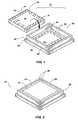
- FIG. 2is a perspective view of the semiconductor assembly of FIG. 1 , after the semiconductor die has been positioned in the recess of the interposer;
- FIG. 3is a side cross-sectional view of one embodiment of a semiconductor assembly made in accordance with the principles of the present invention.
- FIG. 3Ais a side cross-sectional view of another embodiment of the upper electrical connection pads and electrical vias of a semiconductor assembly made in accordance with the principles of the present invention
- FIG. 4is a side cross-sectional view of an alternative embodiment of semiconductor assembly made in accordance with the principles of the present invention.
- FIG. 5is a side cross-sectional view of another embodiment of a semiconductor assembly made in accordance with the principles of the present invention.
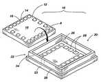
- FIG. 1Several components of a semiconductor assembly 10 in accordance with the principles of the present invention are depicted, in an unassembled manner.
- a semiconductor die 12also referred to as a semiconductor chip, features a number of solder balls 14 attached to the bond pads 16 of the active surface (face) 18 thereof.
- the bond pads 16are arranged in a grid array connection pattern that, along with solder balls 14 , facilitates a BGA-type connection, but it will be appreciated that a SLICC, a PGA, or any other suitable connection method may be used in connection with the bond pads 16 .
- Interposer 20is used for attachment to the semiconductor die 12 .
- Interposer 20includes an upper surface 22 , which features a perimeter wall 24 substantially encircling a recess 26 formed within upper surface 22 and configured to at least partially receive a semiconductor die 12 .
- perimeter wall 24may form a complete structure, but may alternatively include small gaps (shown in dashed lines) therein.
- the perimeter wall 24may be formed continuous with the outer edge 23 of the interposer 20 or it may be inset, as depicted by FIG. 1 , to form a ledge or shoulder 25 at one or more outer edges 23 of the interposer 20 . It is preferred that the interposer 20 be sized as closely as possible to the semiconductor die 12 .
- a semiconductor assembly 10having only a marginally larger size than the bare semiconductor die 12 , conserving area on a substrate to which the entire semiconductor assembly 10 is attached.
- the thickness of such a semiconductor assembly 10may also be only marginally thicker than the bare semiconductor die 12 .
- upper electrical connection pads 28are arranged in a pattern corresponding to the pattern of bond pads 16 of the semiconductor die 12 .
- the solder balls 14 of the BGAare placed on top of and in contact with upper electrical connection pads 28 .
- the installationmay be accomplished by inverting the semiconductor die 12 over the recess 26 , as shown by arrow A.
- FIG. 2the components of the semiconductor assembly 10 illustrated in FIG. 1 are shown with the semiconductor die 12 installed in the recess 26 of the interposer 20 and within the confines of the perimeter wall 24 .
- the bond pads 16 ( FIG. 1 ) of the semiconductor die 12are positioned above their corresponding upper electrical connection pads 28 ( FIG. 1 ) within the recess 26 of the interposer 20 .
- the semiconductor die 12may be joined to the interposer 20 and the bond pads 16 electrically connected to the upper electrical connection pads 28 by reflowing the solder balls 14 .
- a flow space 30is located between the perimeter wall 24 of the interposer 20 and the outer periphery 13 of the semiconductor die 12 , providing access to the recess 26 .
- FIG. 3Illustrated in drawing FIG. 3 is a cross-sectional view of a semiconductor assembly 40 including a semiconductor die 42 installed in a recess 56 of an interposer 50 .
- Perimeter wall 54is formed as the outer edge of the interposer 50 in the embodiment of the invention illustrated in drawing FIG. 3 .
- the bond pads 44 of the semiconductor die 42are attached to the upper electrical connection pads 58 within the recess 56 of the interposer 50 by reflowed solder connections 46 .
- the upper electrical connection pads 58communicate with lower electrical connections 60 on the lower surface 51 of the interposer 50 through electrically conductive traces 59 that pass through the interposer 50 .
- electrically conductive traces 59may be formed from any suitable electrically conductive material, and may be constructed in any suitable manner known to those skilled in the art
- the interposer 50may be formed using an epoxy-glass laminate such as FR-4.
- the interposer 50may be formed by laminating layers of FR-4 together to form the surfaces, perimeter walls 54 and recess 56 of the interposer 50 .
- Upper electrical connection pads 58 and lower electrical connections 60may be formed through the additive or subtractive etching of a conductive layer upon the laminate.
- Electrically conductive traces 59 through the interposer 50 bodymay be formed through laminating conductive material within the interposer 50 .
- holes or recessesmay be created within the interposer during lamination thereof or by mechanical means such as drilling.
- the holesmay be used as vias 62 ( FIG. 3A ), or may be filled with a conductive material to form the electrically conductive traces 59 .
- FIG. 3AIllustrated in drawing FIG. 3A is another alternative embodiment structure for the upper electrical connection pads 58 and the electrically conductive traces 59 illustrated in drawing FIG. 3 .
- a number of vias 62are accessible within the recess 56 of the interposer 50 , in a pattern corresponding to the bond pads 44 of the semiconductor die 42 . Vias 62 connect to the lower electrical connections 60 of the interposer 50 . As shown, once the solder connections 46 are formed by reflowing, the vias 62 are filled with solder, electrically coupling the bond pads 44 to the lower electrical connections 60 .
- the lower electrical connections 60are preferably formed into a standard pattern to provide a standardized connection “footprint,” facilitating the electrical connection of semiconductor assemblies 40 including semiconductor dice having bond pads 44 of various different connection patterns to a substrate, or a testing device, with a fixed connection pattern.
- Interposer 50may include upper electrical connection pads 58 that are formed to correspond to different bond pad arrangements of different semiconductor dice. This can be accomplished in a number of ways. One set of alternate upper electrical connection pads, represented by 58 A and 58 B, communicates with a single lower electrical connection 60 through electrically conductive traces 59 A and 59 B.
- Another set of alternate electrical connection pads represented by 58 C and 58 Dare connected by an electrically conductive trace 61 on the surface of the interposer recess 56 , resulting in connection to a single electrically conductive trace 59 .
- Electrically conductive trace 61may be formed at the same time as the upper electrical connection pads 58 .
- Other possible alternativesinclude alternate sets where a number of upper electrical connection pads 58 are connected to one or more electrically conductive traces 59 . Alternate sets may be formed in connection with vias 62 ( FIG. 3A ) through connection of an upper electrical connection pad 58 to the via 62 through an electrically conductive trace 61 or 59 , or by a channel 63 ( FIG. 3A ) which allows solder to flow to the via 62 .
- a number of alternate sets of upper electrical connection pads 58can be formed into alternate arrays and that, while alternate electrical connections include alternate pairs of upper electrical connections, they may also include three, four or any other number of sets of alternate electrical connection pads.
- the arrangement of the lower electrical connections 60 in a single, standard footprintallows for decreased production costs in assembling products utilizing the complete packaged semiconductor assemblies 40 formed as part of the present invention.
- the interposer 50may also include additional electrical components needed to allow alternative semiconductor dies 42 to be functionally used in a complete semiconductor assembly 40 including the interposer 50 .
- the space 70 between the semiconductor die 42 and the interposer 50is filled by flowing an underfill encapsulant thereinto.
- Arrows 72show the flow of the underfill encapsulant.
- the perimeter walls 54act to restrain the flow of the underfill encapsulant to locations within the recess 56 and thereover.
- the distance between the perimeter wall 54 and the semiconductor die 42determines the rate at which the underfill encapsulant may flow through and into the space 70 , and between the semiconductor die 42 and the upper surface of the interposer recess 56 .
- the distance between each side of the semiconductor die 42 and its corresponding perimeter wall 54is substantially equal, creating substantially equal flow restriction along each of the side surfaces of the semiconductor die 42 .
- the underfill encapsulantis flowed into the space 70 along the entire perimeter of the semiconductor die 42 .
- the low viscosity underfill encapsulantwill flow laterally between the soldered electrical connections 46 between the semiconductor die 42 and the interposer 50 by capillary action, or “wicking,” to substantially fill the space 70 .
- Flow of the underfill encapsulantis increased relative to a higher viscosity underfill encapsulant.
- the underfill encapsulantdoes not need to be injected at elevated pressure and no vacuum is required. In this way, the occurrence of underfill defects can be reduced, while additional steps and equipment are not required.
- FIG. 4Illustrated in drawing FIG. 4 is a cross-sectional view of a semiconductor assembly 80 made in accordance with the principles of the present invention.
- a semiconductor die 82is installed in flip chip fashion at least partially within a recess 96 of an interposer 90 that includes a perimeter wall 92 .
- An underfill encapsulant 102has been flowed as described above between the semiconductor die 82 and the interposer 90 .
- the electrical connections 86 between the bond pads 84 of the semiconductor die 82 and the upper electrical connection pads 98 of the interposer 90are completely encapsulated, protecting the connections from moisture and contamination.
- the underfill encapsulant 102has been flowed to the point where the entire first surface 83 of the semiconductor die 82 was wetted and thereby bound thereto.
- a heat sink 87(shown in dashed lines), or other structure, may then be installed upon the second surface 85 of the semiconductor die 82 .
- the underfill encapsulant 102extends only to the first surface 83 of the semiconductor die 82 , it is preferred that the perimeter wall 92 be equal to or less than the height of the second surface 85 of the installed semiconductor die 82 to facilitate the installation of a heat sink or other structure onto the second surface 85 of semiconductor die 82 .
- the underfill encapsulant 102may fill the entire available space around the semiconductor die 82 , instead of forming fillets around the base of the semiconductor die 82 .
- the present inventionprovides for the use of underfill encapsulants of such low viscosity that such fillets may not form. This increases the ability of the encapsulant to flow throughout the connections, reducing the occurrence of defects. It will be appreciated, however, that the principles of the present invention extend to the use of lower viscosity underfill encapsulants that retain the ability to form fillets, and the use of such underfill encapsulants is within the scope of the present invention.
- interposer 90including a ledge 95 on the upper surface thereof and located outside the perimeter wall 92 .
- ledge 95may carry additional electrical connection pads that may provide additional connection points or testing points for the semiconductor assembly 80 .
- FIG. 5Illustrated in drawing FIG. 5 is a cross-sectional view of another embodiment of a semiconductor assembly 110 , made in accordance with the principles of the present invention.
- a semiconductor die 112is positioned within a recess 126 of and flip chip bonded to an interposer 120 .
- An underfill encapsulant 140has been flowed between the semiconductor die 112 and the interposer 120 , as described above.
- the electrical connections 116 between the bond pads 114 of the semiconductor die 112 and their corresponding upper electrical connection pads 128 of the interposer 120are substantially encapsulated, protecting the electrical connections 116 from moisture and contamination.
- FIG. 5is a cross-sectional view of another embodiment of a semiconductor assembly 110 , made in accordance with the principles of the present invention.
- a semiconductor die 112is positioned within a recess 126 of and flip chip bonded to an interposer 120 .
- An underfill encapsulant 140has been flowed between the semiconductor die 112 and the interposer
- the semiconductor die 112 of the embodiment of the invention illustrated in drawing FIG. 5is completely encapsulated, protecting it from moisture entry, contamination, and delamination. A separate glob top epoxy is not needed, eliminating both an extra step in package preparation and the need for additional materials.
- a semiconductor assembly made in accordance with the principles of the present inventionmay be attached or secured relative to a substrate (not shown) via discrete conductive elements secured to the lower electrical connection pads (represented at 60 , 100 and 130 in the respective drawings).
- the substratecan be part of a final product into which the assembly is to be incorporated, or it may be for testing the semiconductor die. Alternatively, the assembly may be tested through the lower electrical contacts prior to attachment to a substrate.
- the assemblymay be attached to the substrate using any COB technique known to those skilled in the art, but it is preferred to use a flip chip type of attachment, preserving the advantages of this space-saving attachment, while including the advantages of the present invention.
- the present inventionincludes a method of forming a semiconductor assembly including an underfilled flip chip mounted die and perimeter walled interposer, comprising:
- the present inventionincludes a method of forming a semiconductor assembly including an interposer with a standardized footprint comprising:
- Perimeter walled interposersmay be sized only slightly larger than the semiconductor chip and may include a flip chip type of attachment array or other connection pattern on the lower surface thereof. Such an arrangement conserves real estate by allowing flip chip attachment of the entire structure to a substrate in an area only slightly larger than the semiconductor die. The need for applying a positive or negative pressure during assembly to facilitate flow of the underfill encapsulant and the need for a glob top encapsulant are eliminated, resulting in lower manufacturing costs.
- the array of electrical connection pads in the interposer recesscan be designed to facilitate electrical connection of the interposer with a number of alternative bond pad arrangements of different semiconductor dice.
- the resulting packageshave a common footprint for attachment to a substrate.
- Alternative semiconductor dice capable of performing the same or similar functionscan be easily substituted in the semiconductor assembly, without a need for changing the connection pattern on the substrate. This allows for more efficient installation, or testing, of the semiconductor assemblies, reducing the potential costs and time involved in utilizing the equivalent assemblies in the manufacture of products.
Landscapes
- Engineering & Computer Science (AREA)
- Computer Hardware Design (AREA)
- Microelectronics & Electronic Packaging (AREA)
- Power Engineering (AREA)
- Physics & Mathematics (AREA)
- Condensed Matter Physics & Semiconductors (AREA)
- General Physics & Mathematics (AREA)
- Manufacturing & Machinery (AREA)
- Chemical & Material Sciences (AREA)
- Dispersion Chemistry (AREA)
- Wire Bonding (AREA)
Abstract
Description
- This application is a continuation of application Ser. No. 10/133,250, filed Apr. 26, 2002, the disclosure of which is incorporated by reference herein, which is a divisional of application Ser. No. 09/934,278, filed Aug. 21, 2001, now U.S. Pat. No. 6,573,592, issued Jun. 3, 2003.
- Field of the Invention: The present invention relates to ball grid array (“BGA”) semiconductor packages and methods of attaching, encapsulating and evaluating the same. In particular, the present invention relates to interposers for mounting a BGA semiconductor die to a carrier substrate with which the BGA semiconductor die is in electrical communication, such that an underfill encapsulant may be flowed between the BGA semiconductor die and the interposer. The BGA semiconductor die may be encapsulated within the interposer to form a complete semiconductor die package. The interposer may be constructed such that semiconductor die having different patterns of BGAs may be mounted on identical substrates without a need for substrate alteration.
- Definitions: The following terms and acronyms will be used throughout the application and are defined as follows:
- BGA—Ball Grid Array: An array of minute solder balls disposed on an attachment surface of a semiconductor die, interposer, or semiconductor package wherein the solder balls are reflowed for simultaneous attachment and electrical communication with a substrate, such as a printed circuit board.
- COB—Chip on Board: The techniques used to attach semiconductor dice to substrates, including flip chip attachment, wirebonding, and tape automated bonding (“TAB”).
- Flip Chip: A semiconductor die or chip having bumped bond pads on the active surface of the die and is intended for facedown mounting.
- Flip Chip Attachment: A method of attaching a semiconductor die to a substrate in which the die is flipped so that the connecting conductor pads on the active surface of the die are set on mirror image pads on the substrate and bonded by reflowing solder.
- Glob Top: A glob of encapsulant material (usually epoxy or silicone or a combination thereof) surrounding a semiconductor die in the COB assembly process.
- Low Viscosity Encapsulant: An encapsulant material suitable for use as an underfill (usually epoxy or silicone or a combination thereof) which, prior to curing, has a relatively low viscosity, such that it may be directed to flow into and through an array of connecting bond pads of a semiconductor die attached to a substrate, with substantially no voids left therein, without the use of a pressure differential.
- PGA—Pin Grid Array: An array of small pins extending substantially perpendicularly from the major plane of a semiconductor die, interposer, or semiconductor package, wherein the pins conform to a specific arrangement for attachment to a substrate.
- SLICC—Slightly Larger than Integrated Circuit Carrier: An array of minute solder balls disposed on an attachment surface of a semiconductor die, interposer, or semiconductor package similar to a BGA, but having a smaller solder ball pitch and diameter than a BGA.
- Flip chip attachment consists of attaching a semiconductor die, generally having a BGA, a SLICC or a PGA, to a printed circuit board or other substrate. With the BGA or the SLICC, the solder ball arrangement on the semiconductor die must be a mirror image of the connecting bond pads on the substrate such that a precise connection is made. The semiconductor die is bonded to the substrate by reflowing the solder balls. With the PGA, the pin arrangement of the semiconductor die must be a mirror image of the pin recesses on the substrate. After insertion, the semiconductor die is generally bonded by soldering the pins into place.
- Once the semiconductor die has been flip chip attached to the substrate, an underfill encapsulant is generally disposed between the semiconductor die and the substrate. The underfill encapsulant is generally a fluid epoxy that may be flowed into the connection space between the semiconductor die and substrate, laterally between the soldered electrical connections. Typically, the underfill encapsulant is allowed to flow until fillets of underfill encapsulant are formed around the sides of the semiconductor die. In order to form the fillets and to prevent the underfill encapsulant from flowing further and covering other portions of the substrate, thereby reducing the “real estate” (die surface area) used by the semiconductor die connection, it has been necessary to use underfill encapsulants which have a relatively high viscosity.
- Once cured, the underfill encapsulant serves multiple functions. It compensates for the difference in coefficient of thermal expansion between the substrate and the semiconductor die. It also protects the solder bumps from environmental contaminants. However, flowing an underfill encapsulant with relatively high viscosity into the connection space raises further problems. More viscous underfill encapsulants are often unable to flow in between all the connections within the connection space. Empty areas, or voids, occurring when bubbles are trapped within the connection space are common. Delaminations, where the high viscosity underfill encapsulant fails to wet and adhere to a surface, also occur. Such defects can lead to the early failure of the semiconductor die when in operation.
- Attempts have been made to reduce the number of defects in the underfilling process. Typically, a vacuum is applied to facilitate the flow of underfill encapsulant into the connection space. Alternatively, or in addition to the application of a vacuum, a highly viscous underfill encapsulant may be injected under elevated pressure. Even where these techniques are used, defects can still occur. Applying a vacuum or elevated pressure can stress the solder connections, resulting in weakening or breakage thereof. The manufacturing cost of the package is also increased as additional processing steps as well as additional equipment for maintaining and applying the pressure differences are required.
- With wire-bond or TAB adapted dies, a molded carrier ring may be used to protect a portion of the leads as they extend out from the semiconductor die. This is accomplished by placing a molded carrier ring around the die, with the leads protruding therefrom, then filling the molded carrier ring with an encapsulant material. The ends of the leads protruding from the ring are available for testing or connection to a substrate. While the die itself is protected, the exposed lead ends remain susceptible to breakage, moisture and contamination. Even this limited protection cannot be used with flip chip adapted semiconductor die, as the connection pads do not extend out parallel to the plane of the die.
- Therefore, it would be advantageous to develop an apparatus and method that allow for use of a relatively low viscosity underfill encapsulant with flip chip attachment for semiconductor dice, reducing the rate of underfill defects while eliminating the need for a vacuum or pressurized injection. It would further be advantageous for such an apparatus and method to provide a standard connection pattern allowing for semiconductor dice having different connection patterns to be attached to a common substrate having a single set of connection terminals.
- The present invention includes apparatus and methods for preparing semiconductor packages, or assemblies. An interposer having a perimeter wall surrounding a recess on an upper surface thereof includes an array of electrical connection pads within the recess. A semiconductor die can be flip chip attached, making electrical contact through the electrical connection pads to a number of other electrical contacts accessible elsewhere on the interposer, preferably on the lower surface thereof. A low viscosity underfill encapsulant is disposed between the semiconductor die and the interposer by flowing into the space between the die and the perimeter wall of the interposer. The underfill encapsulant flows throughout the connection array by capillary action, without the assistance of either positive or negative pressure. The underfill encapsulant may be flowed until the underfill is complete, or until the entire semiconductor die is encapsulated within the interposer.
- In the drawings, which depict the best mode presently known for carrying out the invention:
FIG. 1 is a perspective view of a semiconductor die which is about to be attached to an interposer in accordance with the present invention to form a semiconductor assembly made in accordance with the present invention;FIG. 2 is a perspective view of the semiconductor assembly ofFIG. 1 , after the semiconductor die has been positioned in the recess of the interposer;FIG. 3 is a side cross-sectional view of one embodiment of a semiconductor assembly made in accordance with the principles of the present invention;FIG. 3A is a side cross-sectional view of another embodiment of the upper electrical connection pads and electrical vias of a semiconductor assembly made in accordance with the principles of the present invention;FIG. 4 is a side cross-sectional view of an alternative embodiment of semiconductor assembly made in accordance with the principles of the present invention; andFIG. 5 is a side cross-sectional view of another embodiment of a semiconductor assembly made in accordance with the principles of the present invention.- Reference will now be made to drawing
FIG. 1 . Several components of asemiconductor assembly 10 in accordance with the principles of the present invention are depicted, in an unassembled manner. A semiconductor die12, also referred to as a semiconductor chip, features a number ofsolder balls 14 attached to thebond pads 16 of the active surface (face)18 thereof. As depicted, thebond pads 16 are arranged in a grid array connection pattern that, along withsolder balls 14, facilitates a BGA-type connection, but it will be appreciated that a SLICC, a PGA, or any other suitable connection method may be used in connection with thebond pads 16. - An
interposer 20 is used for attachment to the semiconductor die12.Interposer 20 includes anupper surface 22, which features aperimeter wall 24 substantially encircling arecess 26 formed withinupper surface 22 and configured to at least partially receive asemiconductor die 12. As shown inFIG. 1 ,perimeter wall 24 may form a complete structure, but may alternatively include small gaps (shown in dashed lines) therein. Theperimeter wall 24 may be formed continuous with theouter edge 23 of theinterposer 20 or it may be inset, as depicted byFIG. 1 , to form a ledge orshoulder 25 at one or moreouter edges 23 of theinterposer 20. It is preferred that theinterposer 20 be sized as closely as possible to the semiconductor die12. This results in asemiconductor assembly 10 having only a marginally larger size than the bare semiconductor die12, conserving area on a substrate to which theentire semiconductor assembly 10 is attached. The thickness of such asemiconductor assembly 10 may also be only marginally thicker than the bare semiconductor die12. - Within the
recess 26 are a number of upperelectrical connection pads 28, which are arranged in a pattern corresponding to the pattern ofbond pads 16 of the semiconductor die12. When the semiconductor die12 is installed in therecess 26, thesolder balls 14 of the BGA, as illustrated in the embodiment of the invention of drawingFIG. 1 , are placed on top of and in contact with upperelectrical connection pads 28. The installation may be accomplished by inverting the semiconductor die12 over therecess 26, as shown by arrow A. - Turning to drawing
FIG. 2 , the components of thesemiconductor assembly 10 illustrated inFIG. 1 are shown with the semiconductor die12 installed in therecess 26 of theinterposer 20 and within the confines of theperimeter wall 24. The bond pads16 (FIG. 1 ) of the semiconductor die12 are positioned above their corresponding upper electrical connection pads28 (FIG. 1 ) within therecess 26 of theinterposer 20. In embodiments using a BGA or SLICC arrangement, the semiconductor die12 may be joined to theinterposer 20 and thebond pads 16 electrically connected to the upperelectrical connection pads 28 by reflowing thesolder balls 14. - As shown in drawing
FIG. 2 , when the semiconductor die12 is installed in therecess 26 of theinterposer 20, aflow space 30 is located between theperimeter wall 24 of theinterposer 20 and theouter periphery 13 of the semiconductor die12, providing access to therecess 26. - Illustrated in drawing
FIG. 3 is a cross-sectional view of asemiconductor assembly 40 including asemiconductor die 42 installed in arecess 56 of aninterposer 50.Perimeter wall 54 is formed as the outer edge of theinterposer 50 in the embodiment of the invention illustrated in drawingFIG. 3 . Thebond pads 44 of the semiconductor die42 are attached to the upperelectrical connection pads 58 within therecess 56 of theinterposer 50 by reflowedsolder connections 46. The upperelectrical connection pads 58 communicate with lowerelectrical connections 60 on thelower surface 51 of theinterposer 50 through electricallyconductive traces 59 that pass through theinterposer 50. - While it will be appreciated that electrically
conductive traces 59 may be formed from any suitable electrically conductive material, and may be constructed in any suitable manner known to those skilled in the art, in some possible embodiments of the present invention, theinterposer 50 may be formed using an epoxy-glass laminate such as FR-4. In such embodiments, theinterposer 50 may be formed by laminating layers of FR-4 together to form the surfaces,perimeter walls 54 andrecess 56 of theinterposer 50. Upperelectrical connection pads 58 and lowerelectrical connections 60 may be formed through the additive or subtractive etching of a conductive layer upon the laminate. Electrically conductive traces59 through theinterposer 50 body may be formed through laminating conductive material within theinterposer 50. Alternatively, holes or recesses may be created within the interposer during lamination thereof or by mechanical means such as drilling. The holes may be used as vias62 (FIG. 3A ), or may be filled with a conductive material to form the electrically conductive traces59. - Illustrated in drawing
FIG. 3A is another alternative embodiment structure for the upperelectrical connection pads 58 and the electrically conductive traces59 illustrated in drawingFIG. 3 . A number ofvias 62 are accessible within therecess 56 of theinterposer 50, in a pattern corresponding to thebond pads 44 of the semiconductor die42.Vias 62 connect to the lowerelectrical connections 60 of theinterposer 50. As shown, once thesolder connections 46 are formed by reflowing, thevias 62 are filled with solder, electrically coupling thebond pads 44 to the lowerelectrical connections 60. - Returning to drawing
FIG. 3 , the lowerelectrical connections 60 are preferably formed into a standard pattern to provide a standardized connection “footprint,” facilitating the electrical connection ofsemiconductor assemblies 40 including semiconductor dice havingbond pads 44 of various different connection patterns to a substrate, or a testing device, with a fixed connection pattern.Interposer 50 may include upperelectrical connection pads 58 that are formed to correspond to different bond pad arrangements of different semiconductor dice. This can be accomplished in a number of ways. One set of alternate upper electrical connection pads, represented by58A and58B, communicates with a single lowerelectrical connection 60 through electricallyconductive traces conductive trace 61 on the surface of theinterposer recess 56, resulting in connection to a single electricallyconductive trace 59. Electricallyconductive trace 61 may be formed at the same time as the upperelectrical connection pads 58. Other possible alternatives include alternate sets where a number of upperelectrical connection pads 58 are connected to one or more electrically conductive traces59. Alternate sets may be formed in connection with vias62 (FIG. 3A ) through connection of an upperelectrical connection pad 58 to the via62 through an electricallyconductive trace FIG. 3A ) which allows solder to flow to the via62. It will be appreciated that a number of alternate sets of upperelectrical connection pads 58 can be formed into alternate arrays and that, while alternate electrical connections include alternate pairs of upper electrical connections, they may also include three, four or any other number of sets of alternate electrical connection pads. - The arrangement of the lower
electrical connections 60 in a single, standard footprint allows for decreased production costs in assembling products utilizing the complete packagedsemiconductor assemblies 40 formed as part of the present invention. Theinterposer 50 may also include additional electrical components needed to allow alternative semiconductor dies42 to be functionally used in acomplete semiconductor assembly 40 including theinterposer 50. - The
space 70 between the semiconductor die42 and theinterposer 50 is filled by flowing an underfill encapsulant thereinto.Arrows 72 show the flow of the underfill encapsulant. Theperimeter walls 54 act to restrain the flow of the underfill encapsulant to locations within therecess 56 and thereover. The distance between theperimeter wall 54 and the semiconductor die42 determines the rate at which the underfill encapsulant may flow through and into thespace 70, and between the semiconductor die42 and the upper surface of theinterposer recess 56. Preferably, the distance between each side of the semiconductor die42 and itscorresponding perimeter wall 54 is substantially equal, creating substantially equal flow restriction along each of the side surfaces of the semiconductor die42. This allows for a low viscosity underfill encapsulant to be used and to be flowed in along two or more sides of the semiconductor die42 at the same time. Preferably, the underfill encapsulant is flowed into thespace 70 along the entire perimeter of the semiconductor die42. The low viscosity underfill encapsulant will flow laterally between the solderedelectrical connections 46 between the semiconductor die42 and theinterposer 50 by capillary action, or “wicking,” to substantially fill thespace 70. Flow of the underfill encapsulant is increased relative to a higher viscosity underfill encapsulant. The underfill encapsulant does not need to be injected at elevated pressure and no vacuum is required. In this way, the occurrence of underfill defects can be reduced, while additional steps and equipment are not required. - Illustrated in drawing
FIG. 4 is a cross-sectional view of asemiconductor assembly 80 made in accordance with the principles of the present invention. A semiconductor die82 is installed in flip chip fashion at least partially within arecess 96 of aninterposer 90 that includes aperimeter wall 92. Anunderfill encapsulant 102 has been flowed as described above between the semiconductor die82 and theinterposer 90. Theelectrical connections 86 between thebond pads 84 of the semiconductor die82 and the upperelectrical connection pads 98 of theinterposer 90 are completely encapsulated, protecting the connections from moisture and contamination. Theunderfill encapsulant 102 has been flowed to the point where the entirefirst surface 83 of the semiconductor die82 was wetted and thereby bound thereto. This reduces the physical stress on the electrical connections while leaving thesecond surface 85 of the semiconductor die82 exposed. A heat sink87 (shown in dashed lines), or other structure, may then be installed upon thesecond surface 85 of the semiconductor die82. In embodiments of the present invention where theunderfill encapsulant 102 extends only to thefirst surface 83 of the semiconductor die82, it is preferred that theperimeter wall 92 be equal to or less than the height of thesecond surface 85 of the installed semiconductor die82 to facilitate the installation of a heat sink or other structure onto thesecond surface 85 of semiconductor die82. - As shown in drawing
FIG. 4 , theunderfill encapsulant 102 may fill the entire available space around the semiconductor die82, instead of forming fillets around the base of the semiconductor die82. The present invention provides for the use of underfill encapsulants of such low viscosity that such fillets may not form. This increases the ability of the encapsulant to flow throughout the connections, reducing the occurrence of defects. It will be appreciated, however, that the principles of the present invention extend to the use of lower viscosity underfill encapsulants that retain the ability to form fillets, and the use of such underfill encapsulants is within the scope of the present invention. - Also illustrated in drawing
FIG. 4 is aninterposer 90 including aledge 95 on the upper surface thereof and located outside theperimeter wall 92. In some variations ofinterposer 90,ledge 95 may carry additional electrical connection pads that may provide additional connection points or testing points for thesemiconductor assembly 80. - Illustrated in drawing
FIG. 5 is a cross-sectional view of another embodiment of asemiconductor assembly 110, made in accordance with the principles of the present invention. A semiconductor die112 is positioned within arecess 126 of and flip chip bonded to aninterposer 120. Anunderfill encapsulant 140 has been flowed between the semiconductor die112 and theinterposer 120, as described above. Theelectrical connections 116 between thebond pads 114 of the semiconductor die112 and their corresponding upperelectrical connection pads 128 of theinterposer 120 are substantially encapsulated, protecting theelectrical connections 116 from moisture and contamination. Unlike the embodiment of the present invention illustrated in drawingFIG. 4 , in this embodiment of the invention, once thefirst surface 113 of the semiconductor die112 is wetted by theunderfill encapsulant 140, further underfill encapsulant is flowed into therecess 126, until thesecond surface 115 of the semiconductor die112 is also encapsulated within theunderfill encapsulant 140. Theperimeter wall 124 is greater in height than thesecond surface 115 of the installed semiconductor die112 to facilitate encapsulation of thesecond surface 115. - Once the
underfill encapsulant 140 has cured, the semiconductor die112 of the embodiment of the invention illustrated in drawingFIG. 5 is completely encapsulated, protecting it from moisture entry, contamination, and delamination. A separate glob top epoxy is not needed, eliminating both an extra step in package preparation and the need for additional materials. - A semiconductor assembly made in accordance with the principles of the present invention, such as those embodiments of the present invention illustrated in drawing
FIGS. 3, 4 and5, among others, may be attached or secured relative to a substrate (not shown) via discrete conductive elements secured to the lower electrical connection pads (represented at60,100 and130 in the respective drawings). The substrate can be part of a final product into which the assembly is to be incorporated, or it may be for testing the semiconductor die. Alternatively, the assembly may be tested through the lower electrical contacts prior to attachment to a substrate. The assembly may be attached to the substrate using any COB technique known to those skilled in the art, but it is preferred to use a flip chip type of attachment, preserving the advantages of this space-saving attachment, while including the advantages of the present invention. - In accordance with the description provided herein, the present invention includes a method of forming a semiconductor assembly including an underfilled flip chip mounted die and perimeter walled interposer, comprising:
- providing an interposer having an upper surface and an opposite lower surface, a perimeter wall protruding from the upper surface and substantially encircling at least a portion of the upper surface to form a recess, the recess having at least one upper electrical contact pad located therein;
- providing a semiconductor die having a first surface and a second surface, the first surface including at least one bond pad thereon;
- positioning the semiconductor die at least partially within the receptacle of the interposer within the recess such that the at least one bond pad is in electrical communication with the at least one upper electrical contact pad on the upper surface of the interposer and at least some of the surface area of the upper surface of the interposer is accessible between a periphery of the semiconductor die and the perimeter wall of the interposer; and
- disposing an underfill encapsulant onto the accessible surface area such that the underfill encapsulant flows between the first surface of said semiconductor die and the upper surface of said interposer between the periphery of the semiconductor die and the perimeter wall, encapsulating the at least one upper electrical contact pad and the at least one bond pad within the underfill encapsulant.
- Further, it will be appreciated that the present invention includes a method of forming a semiconductor assembly including an interposer with a standardized footprint comprising:
- providing an interposer comprising an upper surface, a perimeter wall substantially encircling the upper surface, and a recess formed by the upper surface and the perimeter wall having at least two upper electrical contacts located on the upper surface, within the recess, a pair of alternate upper electrical contacts, a lower surface having at least a first lower electrical connection located thereon, at least the first lower electrical connection in electrical connection with a first upper electrical connection and a second upper electrical connection;
- positioning a semiconductor die at least partially within the recess and electrically connecting at least one bond pad thereof to one of the at least two upper electrical contacts.
- It is readily evident that semiconductor assemblies made in accordance with the principles of the present invention have a reduced number of defects and are capable of being manufactured with reduced steps in assembly. Perimeter walled interposers may be sized only slightly larger than the semiconductor chip and may include a flip chip type of attachment array or other connection pattern on the lower surface thereof. Such an arrangement conserves real estate by allowing flip chip attachment of the entire structure to a substrate in an area only slightly larger than the semiconductor die. The need for applying a positive or negative pressure during assembly to facilitate flow of the underfill encapsulant and the need for a glob top encapsulant are eliminated, resulting in lower manufacturing costs.
- The array of electrical connection pads in the interposer recess can be designed to facilitate electrical connection of the interposer with a number of alternative bond pad arrangements of different semiconductor dice. The resulting packages have a common footprint for attachment to a substrate. Alternative semiconductor dice capable of performing the same or similar functions can be easily substituted in the semiconductor assembly, without a need for changing the connection pattern on the substrate. This allows for more efficient installation, or testing, of the semiconductor assemblies, reducing the potential costs and time involved in utilizing the equivalent assemblies in the manufacture of products.
- It will be apparent that details of the apparatus and methods herein described can be varied considerably without departing from the concept and scope of the invention. The claims alone define the scope of the invention as conceived and as described herein.
Claims (26)
Priority Applications (1)
| Application Number | Priority Date | Filing Date | Title |
|---|---|---|---|
| US11/168,776US7279366B2 (en) | 2001-08-21 | 2005-06-28 | Method for assembling semiconductor die packages with standard ball grid array footprint |
Applications Claiming Priority (3)
| Application Number | Priority Date | Filing Date | Title |
|---|---|---|---|
| US09/934,278US6573592B2 (en) | 2001-08-21 | 2001-08-21 | Semiconductor die packages with standard ball grid array footprint and method for assembling the same |
| US10/133,250US6939746B2 (en) | 2001-08-21 | 2002-04-26 | Method for assembling semiconductor die packages with standard ball grid array footprint |
| US11/168,776US7279366B2 (en) | 2001-08-21 | 2005-06-28 | Method for assembling semiconductor die packages with standard ball grid array footprint |
Related Parent Applications (1)
| Application Number | Title | Priority Date | Filing Date |
|---|---|---|---|
| US10/133,250ContinuationUS6939746B2 (en) | 2001-08-21 | 2002-04-26 | Method for assembling semiconductor die packages with standard ball grid array footprint |
Publications (2)
| Publication Number | Publication Date |
|---|---|
| US20050255637A1true US20050255637A1 (en) | 2005-11-17 |
| US7279366B2 US7279366B2 (en) | 2007-10-09 |
Family
ID=25465289
Family Applications (4)
| Application Number | Title | Priority Date | Filing Date |
|---|---|---|---|
| US09/934,278Expired - LifetimeUS6573592B2 (en) | 2001-08-21 | 2001-08-21 | Semiconductor die packages with standard ball grid array footprint and method for assembling the same |
| US10/133,250Expired - LifetimeUS6939746B2 (en) | 2001-08-21 | 2002-04-26 | Method for assembling semiconductor die packages with standard ball grid array footprint |
| US10/456,455Expired - LifetimeUS7791205B2 (en) | 2001-08-21 | 2003-06-06 | Interposers for semiconductor die packages with standard ball grill array footprint |
| US11/168,776Expired - LifetimeUS7279366B2 (en) | 2001-08-21 | 2005-06-28 | Method for assembling semiconductor die packages with standard ball grid array footprint |
Family Applications Before (3)
| Application Number | Title | Priority Date | Filing Date |
|---|---|---|---|
| US09/934,278Expired - LifetimeUS6573592B2 (en) | 2001-08-21 | 2001-08-21 | Semiconductor die packages with standard ball grid array footprint and method for assembling the same |
| US10/133,250Expired - LifetimeUS6939746B2 (en) | 2001-08-21 | 2002-04-26 | Method for assembling semiconductor die packages with standard ball grid array footprint |
| US10/456,455Expired - LifetimeUS7791205B2 (en) | 2001-08-21 | 2003-06-06 | Interposers for semiconductor die packages with standard ball grill array footprint |
Country Status (1)
| Country | Link |
|---|---|
| US (4) | US6573592B2 (en) |
Cited By (4)
| Publication number | Priority date | Publication date | Assignee | Title |
|---|---|---|---|---|
| US7691541B2 (en) | 2002-10-21 | 2010-04-06 | Nanoink, Inc. | Methods for additive repair of phase shift masks by selectively depositing nanometer-scale engineered structures on defective phase shifters |
| US20120241956A1 (en)* | 2003-03-11 | 2012-09-27 | Micron Technology, Inc. | Techniques for packaging multiple device components |
| US20170117200A1 (en)* | 2015-10-22 | 2017-04-27 | Amkor Technology, Inc. | Semiconductor device and manufacturing method thereof |
| WO2018048571A1 (en)* | 2016-09-12 | 2018-03-15 | Intel Corporation | A microelectronic interposer for a microelectronic package |
Families Citing this family (49)
| Publication number | Priority date | Publication date | Assignee | Title |
|---|---|---|---|---|
| JP3923258B2 (en)* | 2001-01-17 | 2007-05-30 | 松下電器産業株式会社 | Power control system electronic circuit device and manufacturing method thereof |
| FR2826508B1 (en)* | 2001-06-20 | 2004-05-28 | Alstom | ELECTRONIC POWER MODULE AND POWER COMPONENT FOR FITTING SUCH A MODULE |
| US6573592B2 (en)* | 2001-08-21 | 2003-06-03 | Micron Technology, Inc. | Semiconductor die packages with standard ball grid array footprint and method for assembling the same |
| US6963142B2 (en) | 2001-10-26 | 2005-11-08 | Micron Technology, Inc. | Flip chip integrated package mount support |
| US6762509B2 (en)* | 2001-12-11 | 2004-07-13 | Celerity Research Pte. Ltd. | Flip-chip packaging method that treats an interconnect substrate to control stress created at edges of fill material |
| US7332819B2 (en)* | 2002-01-09 | 2008-02-19 | Micron Technology, Inc. | Stacked die in die BGA package |
| US6891276B1 (en)* | 2002-01-09 | 2005-05-10 | Bridge Semiconductor Corporation | Semiconductor package device |
| FI20021232A0 (en)* | 2002-06-24 | 2002-06-24 | Nokia Corp | Method for manufacturing an electronic unit for a radio system and an electronic unit |
| US6998328B2 (en)* | 2002-11-06 | 2006-02-14 | Irvine Sensors Corp. | Method for creating neo-wafers from singulated integrated circuit die and a device made according to the method |
| US7084492B2 (en)* | 2003-06-30 | 2006-08-01 | Intel Corporation | Underfill and mold compounds including siloxane-based aromatic diamines |
| TWI229928B (en)* | 2003-08-19 | 2005-03-21 | Advanced Semiconductor Eng | Semiconductor package structure |
| CN1868056A (en)* | 2003-10-15 | 2006-11-22 | 皇家飞利浦电子股份有限公司 | Device, system and electric element |
| TWI236747B (en)* | 2004-03-12 | 2005-07-21 | Advanced Semiconductor Eng | Manufacturing process and structure for a flip-chip package |
| DE102004042145A1 (en)* | 2004-08-31 | 2006-03-02 | Infineon Technologies Ag | chip module |
| US7045885B1 (en)* | 2004-12-09 | 2006-05-16 | Hewlett-Packard Development Company, L.P. | Placement of absorbing material in a semiconductor device |
| US9299634B2 (en)* | 2006-05-16 | 2016-03-29 | Broadcom Corporation | Method and apparatus for cooling semiconductor device hot blocks and large scale integrated circuit (IC) using integrated interposer for IC packages |
| US9013035B2 (en)* | 2006-06-20 | 2015-04-21 | Broadcom Corporation | Thermal improvement for hotspots on dies in integrated circuit packages |
| US7812459B2 (en)* | 2006-12-19 | 2010-10-12 | Taiwan Semiconductor Manufacturing Company, Ltd. | Three-dimensional integrated circuits with protection layers |
| US7700414B1 (en) | 2007-02-22 | 2010-04-20 | Unisem (Mauritius) Holdings Limited | Method of making flip-chip package with underfill |
| US7982137B2 (en)* | 2007-06-27 | 2011-07-19 | Hamilton Sundstrand Corporation | Circuit board with an attached die and intermediate interposer |
| US8043893B2 (en) | 2007-09-14 | 2011-10-25 | International Business Machines Corporation | Thermo-compression bonded electrical interconnect structure and method |
| US7868457B2 (en)* | 2007-09-14 | 2011-01-11 | International Business Machines Corporation | Thermo-compression bonded electrical interconnect structure and method |
| US9147665B2 (en)* | 2007-11-06 | 2015-09-29 | Fairchild Semiconductor Corporation | High bond line thickness for semiconductor devices |
| SG142321A1 (en) | 2008-04-24 | 2009-11-26 | Micron Technology Inc | Pre-encapsulated cavity interposer |
| JP4989552B2 (en)* | 2008-05-08 | 2012-08-01 | トヨタ自動車株式会社 | Electronic components |
| TWI421982B (en)* | 2008-11-21 | 2014-01-01 | Advanpack Solutions Pte Ltd | Semiconductor substrate and manufacturing method thereof |
| US8405228B2 (en)* | 2009-03-25 | 2013-03-26 | Stats Chippac Ltd. | Integrated circuit packaging system with package underfill and method of manufacture thereof |
| JP5579402B2 (en)* | 2009-04-13 | 2014-08-27 | ピーエスフォー ルクスコ エスエイアールエル | Semiconductor device, method for manufacturing the same, and electronic device |
| US20140254120A1 (en)* | 2009-10-23 | 2014-09-11 | Fujikura Ltd. | Device packaging structure and device packaging method |
| KR101113501B1 (en)* | 2009-11-12 | 2012-02-29 | 삼성전기주식회사 | Manufacturing method of semiconductor package |
| US8381393B2 (en)* | 2009-12-30 | 2013-02-26 | Intel Corporation | Patch on interposer through PGA interconnect structures |
| JP2011176112A (en)* | 2010-02-24 | 2011-09-08 | Renesas Electronics Corp | Semiconductor integrated circuit and method of manufacturing the same |
| US8598695B2 (en) | 2010-07-23 | 2013-12-03 | Tessera, Inc. | Active chip on carrier or laminated chip having microelectronic element embedded therein |
| TWI424552B (en) | 2010-12-31 | 2014-01-21 | Ind Tech Res Inst | Three dimensional chip stacking package structure |
| JP2012199833A (en)* | 2011-03-22 | 2012-10-18 | Taiyo Yuden Co Ltd | Electronic component, electronic device, and manufacturing method of electronic component |
| US8409923B2 (en)* | 2011-06-15 | 2013-04-02 | Stats Chippac Ltd. | Integrated circuit packaging system with underfill and method of manufacture thereof |
| US8994155B2 (en)* | 2012-07-26 | 2015-03-31 | Taiwan Semiconductor Manufacturing Company, Ltd. | Packaging devices, methods of manufacture thereof, and packaging methods |
| US9006908B2 (en)* | 2012-08-01 | 2015-04-14 | Marvell Israel (M.I.S.L) Ltd. | Integrated circuit interposer and method of manufacturing the same |
| DE102012222959B4 (en)* | 2012-12-12 | 2015-04-02 | Semikron Elektronik Gmbh & Co. Kg | Power component device |
| KR102298728B1 (en) | 2014-08-19 | 2021-09-08 | 삼성전자주식회사 | Semiconductor packages |
| US9679862B2 (en)* | 2014-11-28 | 2017-06-13 | Taiwan Semiconductor Manufacturing Company Ltd. | Semiconductor device having conductive bumps of varying heights |
| CN104619117A (en)* | 2015-02-20 | 2015-05-13 | 王镇山 | Magnetic combined structure between circuit boards |
| USD865689S1 (en)* | 2015-02-20 | 2019-11-05 | Microduino Inc. | Electrical module |
| US11355427B2 (en)* | 2016-07-01 | 2022-06-07 | Intel Corporation | Device, method and system for providing recessed interconnect structures of a substrate |
| US11322449B2 (en)* | 2017-10-31 | 2022-05-03 | Taiwan Semiconductor Manufacturing Co., Ltd. | Package with fan-out structures |
| US10504824B1 (en)* | 2018-09-21 | 2019-12-10 | Taiwan Semiconductor Manufacturing Company, Ltd. | Integrated circuit package and method |
| US11195740B2 (en)* | 2019-04-17 | 2021-12-07 | Micron Technology, Inc. | Methods and apparatus for wafer handling and processing |
| US11139268B2 (en)* | 2019-08-06 | 2021-10-05 | Advanced Semiconductor Engineering, Inc. | Semiconductor package structure and method of manufacturing the same |
| KR20220135447A (en) | 2021-03-30 | 2022-10-07 | 삼성전자주식회사 | Semiconductor package and method of fabricating the same |
Citations (35)
| Publication number | Priority date | Publication date | Assignee | Title |
|---|---|---|---|---|
| US5019673A (en)* | 1990-08-22 | 1991-05-28 | Motorola, Inc. | Flip-chip package for integrated circuits |
| US5258648A (en)* | 1991-06-27 | 1993-11-02 | Motorola, Inc. | Composite flip chip semiconductor device with an interposer having test contacts formed along its periphery |
| US5376584A (en)* | 1992-12-31 | 1994-12-27 | International Business Machines Corporation | Process of making pad structure for solder ball limiting metallurgy having reduced edge stress |
| US5412247A (en)* | 1989-07-28 | 1995-05-02 | The Charles Stark Draper Laboratory, Inc. | Protection and packaging system for semiconductor devices |
| US5436203A (en)* | 1994-07-05 | 1995-07-25 | Motorola, Inc. | Shielded liquid encapsulated semiconductor device and method for making the same |
| US5468999A (en)* | 1994-05-26 | 1995-11-21 | Motorola, Inc. | Liquid encapsulated ball grid array semiconductor device with fine pitch wire bonding |
| US5474458A (en)* | 1993-07-13 | 1995-12-12 | Fujitsu Limited | Interconnect carriers having high-density vertical connectors and methods for making the same |
| US5696033A (en)* | 1995-08-16 | 1997-12-09 | Micron Technology, Inc. | Method for packaging a semiconductor die |
| US5714800A (en)* | 1996-03-21 | 1998-02-03 | Motorola, Inc. | Integrated circuit assembly having a stepped interposer and method |
| US5719440A (en)* | 1995-12-19 | 1998-02-17 | Micron Technology, Inc. | Flip chip adaptor package for bare die |
| US5838061A (en)* | 1996-03-11 | 1998-11-17 | Lg Semicon Co., Ltd. | Semiconductor package including a semiconductor chip adhesively bonded thereto |
| US5847936A (en)* | 1997-06-20 | 1998-12-08 | Sun Microsystems, Inc. | Optimized routing scheme for an integrated circuit/printed circuit board |
| US5855821A (en)* | 1995-12-22 | 1999-01-05 | Johnson Matthey, Inc. | Materials for semiconductor device assemblies |
| US5898224A (en)* | 1997-01-24 | 1999-04-27 | Micron Technology, Inc. | Apparatus for packaging flip chip bare die on printed circuit boards |
| US5942798A (en)* | 1997-11-24 | 1999-08-24 | Stmicroelectronics, Inc. | Apparatus and method for automating the underfill of flip-chip devices |
| US5965933A (en)* | 1996-05-28 | 1999-10-12 | Young; William R. | Semiconductor packaging apparatus |
| US5972734A (en)* | 1997-09-17 | 1999-10-26 | Lsi Logic Corporation | Interposer for ball grid array (BGA) package |
| US6002171A (en)* | 1997-09-22 | 1999-12-14 | Lsi Logic Corporation | Integrated heat spreader/stiffener assembly and method of assembly for semiconductor package |
| US6018462A (en)* | 1997-06-30 | 2000-01-25 | Nec Corporation | Multi-tip module |
| US6031284A (en)* | 1997-03-14 | 2000-02-29 | Lg Semicon Co., Ltd. | Package body and semiconductor chip package using same |
| US6048750A (en)* | 1997-11-24 | 2000-04-11 | Micron Technology, Inc. | Method for aligning and connecting semiconductor components to substrates |
| US6063828A (en)* | 1998-07-02 | 2000-05-16 | National Starch And Chemical Investment Holding Corporation | Underfill encapsulant compositions for use in electronic devices |
| US6081429A (en)* | 1999-01-20 | 2000-06-27 | Micron Technology, Inc. | Test interposer for use with ball grid array packages assemblies and ball grid array packages including same and methods |
| US6238949B1 (en)* | 1999-06-18 | 2001-05-29 | National Semiconductor Corporation | Method and apparatus for forming a plastic chip on chip package module |
| US6238948B1 (en)* | 1999-03-03 | 2001-05-29 | Intel Corporation | Controlled collapse chip connection (C4) integrated circuit package that has a fillet which seals an underfill material |
| US6351391B1 (en)* | 2000-05-15 | 2002-02-26 | International Business Machines Corporation | Signal busses on printed board structures mounting ASIC chips with signal termination resistor devices using planar signal terminating devices |
| US6362525B1 (en)* | 1999-11-09 | 2002-03-26 | Cypress Semiconductor Corp. | Circuit structure including a passive element formed within a grid array substrate and method for making the same |
| US6395124B1 (en)* | 1999-07-30 | 2002-05-28 | 3M Innovative Properties Company | Method of producing a laminated structure |
| US6433412B2 (en)* | 2000-03-17 | 2002-08-13 | Hitachi, Ltd. | Semiconductor device and a method of manufacturing the same |
| US6512176B2 (en)* | 1999-03-17 | 2003-01-28 | Hitachi, Ltd. | Semiconductor device |
| US6534879B2 (en)* | 2000-02-25 | 2003-03-18 | Oki Electric Industry Co., Ltd. | Semiconductor chip and semiconductor device having the chip |
| US6573592B2 (en)* | 2001-08-21 | 2003-06-03 | Micron Technology, Inc. | Semiconductor die packages with standard ball grid array footprint and method for assembling the same |
| US6608379B2 (en)* | 2001-11-02 | 2003-08-19 | Institute Of Microelectronics, Et Al. | Enhanced chip scale package for flip chips |
| US20040026797A1 (en)* | 2002-08-08 | 2004-02-12 | Kun-Ching Chen | Flip chip package substrate |
| US6803646B2 (en)* | 2001-01-26 | 2004-10-12 | Sony Corporation | Semiconductor device having first chip secured within resin layer and second chip secured on resin layer |
Family Cites Families (3)
| Publication number | Priority date | Publication date | Assignee | Title |
|---|---|---|---|---|
| JPH0770553B2 (en)* | 1988-09-26 | 1995-07-31 | 日本電気株式会社 | Method for manufacturing semiconductor integrated circuit device |
| JPH0846079A (en)* | 1994-07-28 | 1996-02-16 | Matsushita Electric Ind Co Ltd | Semiconductor device |
| JPH11354664A (en)* | 1998-06-03 | 1999-12-24 | Sony Chem Corp | Semiconductor device |
- 2001
- 2001-08-21USUS09/934,278patent/US6573592B2/ennot_activeExpired - Lifetime
- 2002
- 2002-04-26USUS10/133,250patent/US6939746B2/ennot_activeExpired - Lifetime
- 2003
- 2003-06-06USUS10/456,455patent/US7791205B2/ennot_activeExpired - Lifetime
- 2005
- 2005-06-28USUS11/168,776patent/US7279366B2/ennot_activeExpired - Lifetime
Patent Citations (37)
| Publication number | Priority date | Publication date | Assignee | Title |
|---|---|---|---|---|
| US5412247A (en)* | 1989-07-28 | 1995-05-02 | The Charles Stark Draper Laboratory, Inc. | Protection and packaging system for semiconductor devices |
| US5019673A (en)* | 1990-08-22 | 1991-05-28 | Motorola, Inc. | Flip-chip package for integrated circuits |
| US5258648A (en)* | 1991-06-27 | 1993-11-02 | Motorola, Inc. | Composite flip chip semiconductor device with an interposer having test contacts formed along its periphery |
| US5376584A (en)* | 1992-12-31 | 1994-12-27 | International Business Machines Corporation | Process of making pad structure for solder ball limiting metallurgy having reduced edge stress |
| US5474458A (en)* | 1993-07-13 | 1995-12-12 | Fujitsu Limited | Interconnect carriers having high-density vertical connectors and methods for making the same |
| US5468999A (en)* | 1994-05-26 | 1995-11-21 | Motorola, Inc. | Liquid encapsulated ball grid array semiconductor device with fine pitch wire bonding |
| US5436203A (en)* | 1994-07-05 | 1995-07-25 | Motorola, Inc. | Shielded liquid encapsulated semiconductor device and method for making the same |
| US5696033A (en)* | 1995-08-16 | 1997-12-09 | Micron Technology, Inc. | Method for packaging a semiconductor die |
| US5789803A (en)* | 1995-08-16 | 1998-08-04 | Micron Technology, Inc. | Semiconductor package |
| US5719440A (en)* | 1995-12-19 | 1998-02-17 | Micron Technology, Inc. | Flip chip adaptor package for bare die |
| US5855821A (en)* | 1995-12-22 | 1999-01-05 | Johnson Matthey, Inc. | Materials for semiconductor device assemblies |
| US5838061A (en)* | 1996-03-11 | 1998-11-17 | Lg Semicon Co., Ltd. | Semiconductor package including a semiconductor chip adhesively bonded thereto |
| US5714800A (en)* | 1996-03-21 | 1998-02-03 | Motorola, Inc. | Integrated circuit assembly having a stepped interposer and method |
| US5965933A (en)* | 1996-05-28 | 1999-10-12 | Young; William R. | Semiconductor packaging apparatus |
| US5898224A (en)* | 1997-01-24 | 1999-04-27 | Micron Technology, Inc. | Apparatus for packaging flip chip bare die on printed circuit boards |
| US6031284A (en)* | 1997-03-14 | 2000-02-29 | Lg Semicon Co., Ltd. | Package body and semiconductor chip package using same |
| US5847936A (en)* | 1997-06-20 | 1998-12-08 | Sun Microsystems, Inc. | Optimized routing scheme for an integrated circuit/printed circuit board |
| US6018462A (en)* | 1997-06-30 | 2000-01-25 | Nec Corporation | Multi-tip module |
| US5972734A (en)* | 1997-09-17 | 1999-10-26 | Lsi Logic Corporation | Interposer for ball grid array (BGA) package |
| US6002171A (en)* | 1997-09-22 | 1999-12-14 | Lsi Logic Corporation | Integrated heat spreader/stiffener assembly and method of assembly for semiconductor package |
| US5942798A (en)* | 1997-11-24 | 1999-08-24 | Stmicroelectronics, Inc. | Apparatus and method for automating the underfill of flip-chip devices |
| US6048750A (en)* | 1997-11-24 | 2000-04-11 | Micron Technology, Inc. | Method for aligning and connecting semiconductor components to substrates |
| US6063828A (en)* | 1998-07-02 | 2000-05-16 | National Starch And Chemical Investment Holding Corporation | Underfill encapsulant compositions for use in electronic devices |
| US6081429A (en)* | 1999-01-20 | 2000-06-27 | Micron Technology, Inc. | Test interposer for use with ball grid array packages assemblies and ball grid array packages including same and methods |
| US6238948B1 (en)* | 1999-03-03 | 2001-05-29 | Intel Corporation | Controlled collapse chip connection (C4) integrated circuit package that has a fillet which seals an underfill material |
| US6512176B2 (en)* | 1999-03-17 | 2003-01-28 | Hitachi, Ltd. | Semiconductor device |
| US6238949B1 (en)* | 1999-06-18 | 2001-05-29 | National Semiconductor Corporation | Method and apparatus for forming a plastic chip on chip package module |
| US6395124B1 (en)* | 1999-07-30 | 2002-05-28 | 3M Innovative Properties Company | Method of producing a laminated structure |
| US6362525B1 (en)* | 1999-11-09 | 2002-03-26 | Cypress Semiconductor Corp. | Circuit structure including a passive element formed within a grid array substrate and method for making the same |
| US6534879B2 (en)* | 2000-02-25 | 2003-03-18 | Oki Electric Industry Co., Ltd. | Semiconductor chip and semiconductor device having the chip |
| US6433412B2 (en)* | 2000-03-17 | 2002-08-13 | Hitachi, Ltd. | Semiconductor device and a method of manufacturing the same |
| US6351391B1 (en)* | 2000-05-15 | 2002-02-26 | International Business Machines Corporation | Signal busses on printed board structures mounting ASIC chips with signal termination resistor devices using planar signal terminating devices |
| US6803646B2 (en)* | 2001-01-26 | 2004-10-12 | Sony Corporation | Semiconductor device having first chip secured within resin layer and second chip secured on resin layer |
| US6573592B2 (en)* | 2001-08-21 | 2003-06-03 | Micron Technology, Inc. | Semiconductor die packages with standard ball grid array footprint and method for assembling the same |
| US6939746B2 (en)* | 2001-08-21 | 2005-09-06 | Micron Technology, Inc. | Method for assembling semiconductor die packages with standard ball grid array footprint |
| US6608379B2 (en)* | 2001-11-02 | 2003-08-19 | Institute Of Microelectronics, Et Al. | Enhanced chip scale package for flip chips |
| US20040026797A1 (en)* | 2002-08-08 | 2004-02-12 | Kun-Ching Chen | Flip chip package substrate |
Cited By (10)
| Publication number | Priority date | Publication date | Assignee | Title |
|---|---|---|---|---|
| US7691541B2 (en) | 2002-10-21 | 2010-04-06 | Nanoink, Inc. | Methods for additive repair of phase shift masks by selectively depositing nanometer-scale engineered structures on defective phase shifters |
| US20120241956A1 (en)* | 2003-03-11 | 2012-09-27 | Micron Technology, Inc. | Techniques for packaging multiple device components |
| US8629558B2 (en)* | 2003-03-11 | 2014-01-14 | Micron Technology, Inc. | Techniques for packaging multiple device components |
| US9559087B2 (en) | 2003-03-11 | 2017-01-31 | Micron Technology, Inc. | Techniques for packaging multiple device components |
| US20170117200A1 (en)* | 2015-10-22 | 2017-04-27 | Amkor Technology, Inc. | Semiconductor device and manufacturing method thereof |
| US9941180B2 (en)* | 2015-10-22 | 2018-04-10 | Amkor Technology, Inc. | Semiconductor device and manufacturing method thereof |
| US10388582B2 (en)* | 2015-10-22 | 2019-08-20 | Amkor Technology, Inc. | Semiconductor device and manufacturing method thereof |
| WO2018048571A1 (en)* | 2016-09-12 | 2018-03-15 | Intel Corporation | A microelectronic interposer for a microelectronic package |
| US10199353B2 (en) | 2016-09-12 | 2019-02-05 | Intel Corporation | Microelectronic interposer for a microelectronic package |
| US10720407B2 (en) | 2016-09-12 | 2020-07-21 | Intel Corporation | Microelectronic interposer for a microelectronic package |
Also Published As
| Publication number | Publication date |
|---|---|
| US20030183950A1 (en) | 2003-10-02 |
| US6939746B2 (en) | 2005-09-06 |
| US7279366B2 (en) | 2007-10-09 |
| US20030038381A1 (en) | 2003-02-27 |
| US7791205B2 (en) | 2010-09-07 |
| US6573592B2 (en) | 2003-06-03 |
| US20030038376A1 (en) | 2003-02-27 |
Similar Documents
| Publication | Publication Date | Title |
|---|---|---|
| US7279366B2 (en) | Method for assembling semiconductor die packages with standard ball grid array footprint | |
| US6492726B1 (en) | Chip scale packaging with multi-layer flip chip arrangement and ball grid array interconnection | |
| EP1432033B1 (en) | Multi-chip module and method of forming | |
| US7145225B2 (en) | Interposer configured to reduce the profiles of semiconductor device assemblies and packages including the same and methods | |
| CN100407422C (en) | Semiconductor device and method for manufacturing the same | |
| US7247934B2 (en) | Multi-chip semiconductor package | |
| US7087460B2 (en) | Methods for assembly and packaging of flip chip configured dice with interposer | |
| US6975035B2 (en) | Method and apparatus for dielectric filling of flip chip on interposer assembly | |
| US6195268B1 (en) | Stacking layers containing enclosed IC chips | |
| KR101166575B1 (en) | Semiconductor multi-package module having wire bond interconnection between stacked packages | |
| US20030064547A1 (en) | High density modularity for IC's | |
| US20060240595A1 (en) | Method and apparatus for flip-chip packaging providing testing capability | |
| US20050263906A1 (en) | Electronic system including a semiconductor device with at least one semiconductor die, a carrier, and an encapsulant that fills a space between the die and the carrier and covers intermediate conductive elements that connect the die and the carrier | |
| US20120020040A1 (en) | Package-to-package stacking by using interposer with traces, and or standoffs and solder balls | |
| US8203849B2 (en) | Semiconductor device and manufacture method thereof | |
| JPH09129670A (en) | Contact high density type ball grid array package for flip chip | |
| TW201351579A (en) | High density 3D package | |
| US12132003B2 (en) | Electronic package and manufacturing method thereof | |
| KR100240748B1 (en) | Semiconductor chip package having substrate and manufacturing method thereof, and stack package | |
| US20120146242A1 (en) | Semiconductor device and method of fabricating the same | |
| KR101227792B1 (en) | Multipackage module having stacked packages with asymmetrically arranged die and molding | |
| US12119296B2 (en) | Encircling a semiconductor device with stacked frames on a substrate | |
| US10896877B1 (en) | System in package with double side mounted board | |
| US10515883B2 (en) | 3D system-level packaging methods and structures | |
| US20250054824A1 (en) | Package structure having dam structure |
Legal Events
| Date | Code | Title | Description |
|---|---|---|---|
| FEPP | Fee payment procedure | Free format text:PAYOR NUMBER ASSIGNED (ORIGINAL EVENT CODE: ASPN); ENTITY STATUS OF PATENT OWNER: LARGE ENTITY | |
| STCF | Information on status: patent grant | Free format text:PATENTED CASE | |
| FPAY | Fee payment | Year of fee payment:4 | |
| FPAY | Fee payment | Year of fee payment:8 | |
| AS | Assignment | Owner name:U.S. BANK NATIONAL ASSOCIATION, AS COLLATERAL AGENT, CALIFORNIA Free format text:SECURITY INTEREST;ASSIGNOR:MICRON TECHNOLOGY, INC.;REEL/FRAME:038669/0001 Effective date:20160426 Owner name:U.S. BANK NATIONAL ASSOCIATION, AS COLLATERAL AGEN Free format text:SECURITY INTEREST;ASSIGNOR:MICRON TECHNOLOGY, INC.;REEL/FRAME:038669/0001 Effective date:20160426 | |
| AS | Assignment | Owner name:MORGAN STANLEY SENIOR FUNDING, INC., AS COLLATERAL AGENT, MARYLAND Free format text:PATENT SECURITY AGREEMENT;ASSIGNOR:MICRON TECHNOLOGY, INC.;REEL/FRAME:038954/0001 Effective date:20160426 Owner name:MORGAN STANLEY SENIOR FUNDING, INC., AS COLLATERAL Free format text:PATENT SECURITY AGREEMENT;ASSIGNOR:MICRON TECHNOLOGY, INC.;REEL/FRAME:038954/0001 Effective date:20160426 | |
| AS | Assignment | Owner name:U.S. BANK NATIONAL ASSOCIATION, AS COLLATERAL AGENT, CALIFORNIA Free format text:CORRECTIVE ASSIGNMENT TO CORRECT THE REPLACE ERRONEOUSLY FILED PATENT #7358718 WITH THE CORRECT PATENT #7358178 PREVIOUSLY RECORDED ON REEL 038669 FRAME 0001. ASSIGNOR(S) HEREBY CONFIRMS THE SECURITY INTEREST;ASSIGNOR:MICRON TECHNOLOGY, INC.;REEL/FRAME:043079/0001 Effective date:20160426 Owner name:U.S. BANK NATIONAL ASSOCIATION, AS COLLATERAL AGEN Free format text:CORRECTIVE ASSIGNMENT TO CORRECT THE REPLACE ERRONEOUSLY FILED PATENT #7358718 WITH THE CORRECT PATENT #7358178 PREVIOUSLY RECORDED ON REEL 038669 FRAME 0001. ASSIGNOR(S) HEREBY CONFIRMS THE SECURITY INTEREST;ASSIGNOR:MICRON TECHNOLOGY, INC.;REEL/FRAME:043079/0001 Effective date:20160426 | |
| AS | Assignment | Owner name:JPMORGAN CHASE BANK, N.A., AS COLLATERAL AGENT, ILLINOIS Free format text:SECURITY INTEREST;ASSIGNORS:MICRON TECHNOLOGY, INC.;MICRON SEMICONDUCTOR PRODUCTS, INC.;REEL/FRAME:047540/0001 Effective date:20180703 Owner name:JPMORGAN CHASE BANK, N.A., AS COLLATERAL AGENT, IL Free format text:SECURITY INTEREST;ASSIGNORS:MICRON TECHNOLOGY, INC.;MICRON SEMICONDUCTOR PRODUCTS, INC.;REEL/FRAME:047540/0001 Effective date:20180703 | |
| AS | Assignment | Owner name:MICRON TECHNOLOGY, INC., IDAHO Free format text:RELEASE BY SECURED PARTY;ASSIGNOR:U.S. BANK NATIONAL ASSOCIATION, AS COLLATERAL AGENT;REEL/FRAME:047243/0001 Effective date:20180629 | |
| MAFP | Maintenance fee payment | Free format text:PAYMENT OF MAINTENANCE FEE, 12TH YEAR, LARGE ENTITY (ORIGINAL EVENT CODE: M1553); ENTITY STATUS OF PATENT OWNER: LARGE ENTITY Year of fee payment:12 | |
| AS | Assignment | Owner name:MICRON TECHNOLOGY, INC., IDAHO Free format text:RELEASE BY SECURED PARTY;ASSIGNOR:MORGAN STANLEY SENIOR FUNDING, INC., AS COLLATERAL AGENT;REEL/FRAME:050937/0001 Effective date:20190731 | |
| AS | Assignment | Owner name:MICRON SEMICONDUCTOR PRODUCTS, INC., IDAHO Free format text:RELEASE BY SECURED PARTY;ASSIGNOR:JPMORGAN CHASE BANK, N.A., AS COLLATERAL AGENT;REEL/FRAME:051028/0001 Effective date:20190731 Owner name:MICRON TECHNOLOGY, INC., IDAHO Free format text:RELEASE BY SECURED PARTY;ASSIGNOR:JPMORGAN CHASE BANK, N.A., AS COLLATERAL AGENT;REEL/FRAME:051028/0001 Effective date:20190731 |