US20050253803A1 - Electric paper display with a thin film transistor active matrix and integrated addressing logic - Google Patents
Electric paper display with a thin film transistor active matrix and integrated addressing logicDownload PDFInfo
- Publication number
- US20050253803A1 US20050253803A1US11/001,925US192504AUS2005253803A1US 20050253803 A1US20050253803 A1US 20050253803A1US 192504 AUS192504 AUS 192504AUS 2005253803 A1US2005253803 A1US 2005253803A1
- Authority
- US
- United States
- Prior art keywords
- thin film
- accordance
- electric display
- coupled
- control logic
- Prior art date
- Legal status (The legal status is an assumption and is not a legal conclusion. Google has not performed a legal analysis and makes no representation as to the accuracy of the status listed.)
- Abandoned
Links
- 239000010409thin filmSubstances0.000titleclaimsabstractdescription41
- 239000011159matrix materialSubstances0.000titleclaimsabstractdescription31
- 239000000872bufferSubstances0.000claimsdescription22
- 239000002245particleSubstances0.000claimsdescription13
- 230000005684electric fieldEffects0.000claimsdescription8
- 239000000975dyeSubstances0.000claimsdescription4
- 239000000976inkSubstances0.000claimsdescription4
- 239000000049pigmentSubstances0.000claimsdescription4
- 229910021417amorphous siliconInorganic materials0.000claimsdescription3
- 239000003086colorantSubstances0.000claimsdescription3
- 239000000126substanceSubstances0.000claimsdescription3
- 239000006185dispersionSubstances0.000claimsdescription2
- 229920001296polysiloxanePolymers0.000claims1
- 239000004973liquid crystal related substanceSubstances0.000description10
- 239000002775capsuleSubstances0.000description6
- 238000010586diagramMethods0.000description6
- 238000005516engineering processMethods0.000description4
- 238000003491arrayMethods0.000description3
- 230000008901benefitEffects0.000description3
- 230000015556catabolic processEffects0.000description3
- GWEVSGVZZGPLCZ-UHFFFAOYSA-NTitan oxideChemical compoundO=[Ti]=OGWEVSGVZZGPLCZ-UHFFFAOYSA-N0.000description2
- 239000012530fluidSubstances0.000description2
- 239000000463materialSubstances0.000description2
- XUIMIQQOPSSXEZ-UHFFFAOYSA-NSiliconChemical compound[Si]XUIMIQQOPSSXEZ-UHFFFAOYSA-N0.000description1
- 238000009125cardiac resynchronization therapyMethods0.000description1
- 239000013078crystalSubstances0.000description1
- 238000011161developmentMethods0.000description1
- 230000018109developmental processEffects0.000description1
- 230000005611electricityEffects0.000description1
- 230000005669field effectEffects0.000description1
- 239000010408filmSubstances0.000description1
- 239000011521glassSubstances0.000description1
- 238000005286illuminationMethods0.000description1
- 239000002184metalSubstances0.000description1
- 238000000034methodMethods0.000description1
- 238000012986modificationMethods0.000description1
- 230000004048modificationEffects0.000description1
- 150000004767nitridesChemical class0.000description1
- 230000003287optical effectEffects0.000description1
- 239000011368organic materialSubstances0.000description1
- 239000000123paperSubstances0.000description1
- 239000013618particulate matterSubstances0.000description1
- 239000004033plasticSubstances0.000description1
- 229910021420polycrystalline siliconInorganic materials0.000description1
- 230000009467reductionEffects0.000description1
- 230000004044responseEffects0.000description1
- 239000004065semiconductorSubstances0.000description1
- 229910052710siliconInorganic materials0.000description1
- 239000010703siliconSubstances0.000description1
- 239000000758substrateSubstances0.000description1
- 230000000007visual effectEffects0.000description1
Images


Classifications
- G—PHYSICS
- G09—EDUCATION; CRYPTOGRAPHY; DISPLAY; ADVERTISING; SEALS
- G09G—ARRANGEMENTS OR CIRCUITS FOR CONTROL OF INDICATING DEVICES USING STATIC MEANS TO PRESENT VARIABLE INFORMATION
- G09G3/00—Control arrangements or circuits, of interest only in connection with visual indicators other than cathode-ray tubes
- G09G3/20—Control arrangements or circuits, of interest only in connection with visual indicators other than cathode-ray tubes for presentation of an assembly of a number of characters, e.g. a page, by composing the assembly by combination of individual elements arranged in a matrix no fixed position being assigned to or needed to be assigned to the individual characters or partial characters
- G09G3/34—Control arrangements or circuits, of interest only in connection with visual indicators other than cathode-ray tubes for presentation of an assembly of a number of characters, e.g. a page, by composing the assembly by combination of individual elements arranged in a matrix no fixed position being assigned to or needed to be assigned to the individual characters or partial characters by control of light from an independent source
- G09G3/3433—Control arrangements or circuits, of interest only in connection with visual indicators other than cathode-ray tubes for presentation of an assembly of a number of characters, e.g. a page, by composing the assembly by combination of individual elements arranged in a matrix no fixed position being assigned to or needed to be assigned to the individual characters or partial characters by control of light from an independent source using light modulating elements actuated by an electric field and being other than liquid crystal devices and electrochromic devices
- G09G3/3453—Control arrangements or circuits, of interest only in connection with visual indicators other than cathode-ray tubes for presentation of an assembly of a number of characters, e.g. a page, by composing the assembly by combination of individual elements arranged in a matrix no fixed position being assigned to or needed to be assigned to the individual characters or partial characters by control of light from an independent source using light modulating elements actuated by an electric field and being other than liquid crystal devices and electrochromic devices based on rotating particles or microelements
- G—PHYSICS
- G09—EDUCATION; CRYPTOGRAPHY; DISPLAY; ADVERTISING; SEALS
- G09G—ARRANGEMENTS OR CIRCUITS FOR CONTROL OF INDICATING DEVICES USING STATIC MEANS TO PRESENT VARIABLE INFORMATION
- G09G2300/00—Aspects of the constitution of display devices
- G09G2300/08—Active matrix structure, i.e. with use of active elements, inclusive of non-linear two terminal elements, in the pixels together with light emitting or modulating elements
- G—PHYSICS
- G09—EDUCATION; CRYPTOGRAPHY; DISPLAY; ADVERTISING; SEALS
- G09G—ARRANGEMENTS OR CIRCUITS FOR CONTROL OF INDICATING DEVICES USING STATIC MEANS TO PRESENT VARIABLE INFORMATION
- G09G2310/00—Command of the display device
- G09G2310/02—Addressing, scanning or driving the display screen or processing steps related thereto
- G09G2310/0264—Details of driving circuits
- G09G2310/0267—Details of drivers for scan electrodes, other than drivers for liquid crystal, plasma or OLED displays
- G—PHYSICS
- G09—EDUCATION; CRYPTOGRAPHY; DISPLAY; ADVERTISING; SEALS
- G09G—ARRANGEMENTS OR CIRCUITS FOR CONTROL OF INDICATING DEVICES USING STATIC MEANS TO PRESENT VARIABLE INFORMATION
- G09G2310/00—Command of the display device
- G09G2310/02—Addressing, scanning or driving the display screen or processing steps related thereto
- G09G2310/0264—Details of driving circuits
- G09G2310/0275—Details of drivers for data electrodes, other than drivers for liquid crystal, plasma or OLED displays, not related to handling digital grey scale data or to communication of data to the pixels by means of a current
Definitions
- an electric visual displayMore particularly, an electric paper display using a thin film transistor active matrix array and integrated addressing logic to control the output of the display is disclosed useful, for example, as point of purchase signs.
- LCDliquid crystal diode
- CRTcathode ray tube
- other electrically-addressable displayswill display an image in response to applied electric signals or fields.
- Such signstypically require a large amount of electricity, since they must provide illumination in order to be visible to a viewer.
- Twisting-cylinder displays, rotary-ball displays and related displayshave numerous advantages over conventional displays, such as LCDs and CRTs, since they are suitable for viewing in ambient light, they retain an image indefinitely in the absence of an applied electric field, and they can be made to be very lightweight and/or flexible.
- LCDs and CRTssince they are suitable for viewing in ambient light, they retain an image indefinitely in the absence of an applied electric field, and they can be made to be very lightweight and/or flexible.
- Such displaysare referred to herein as “electric paper” displays.
- An example of such a displayis a SmartPaperTM display from Gyricon LLC.
- An electronic ink displayincludes at least one capsule filled with a plurality of particles, made of a material such as titania, and a dyed suspending fluid.
- a direct-current electric field of an appropriate polarityis applied across the capsule, the particles move to a viewed surface of the display and scatter light.
- the applied electric fieldis reversed, the particles move to the rear surface of the display and the viewed surface of the display then appears dark.
- Yet another type of electric writeable mediaalso described in U.S. Pat. No. 6,518,949 to Drzaic, includes a first set of particles and a second set of particles in a capsule.
- the first set of particles and the second set of particleshave contrasting optical properties, such as contrasting colors, and can have, for example, differing electrophoretic properties.
- the capsulealso contains a substantially clear fluid.
- the capsulehas electrodes disposed adjacent to it connected to a voltage source, which may provide an alternating-current field or a direct-current field to the capsule.
- a voltage sourcewhich may provide an alternating-current field or a direct-current field to the capsule.
- the first set of particlesmoves toward a first electrode
- the second set of particlesmoves toward a second electrode. If the electric field is reversed, the first set of particles moves toward the second electrode and the second set of particles moves toward the first electrode.
- Other examples of writeable mediainclude liquid crystal diode displays, encapsulated electrophoretic displays, and other displays.
- Electric paper displaysrespond slowly to changes in applied voltage. However, electric paper displays are also generally addressed infrequently. Recent developments in electric paper displays are permitting operation at voltage thresholds of approximately 40V. Current electric displays are driven with crystal silicon integrated circuits in separate packages. Such integrated circuits are costly and increase the size of the display. As a result, new technologies for supplying threshold voltages are being explored.
- a thin film transistor (TFT) active matrix arrayis composed of an array of TFTs.
- a TFTis a Metal-Oxide-Semiconductor Field Effect Transistor (MOSFET) implemented using thin film technology.
- MOSFETMetal-Oxide-Semiconductor Field Effect Transistor
- a TFTuses thin films, which may be made of for example, amorphous silicon (a-Si), polycrystalline silicon (p-Si), or which may be an organic material, and a glass substrate. Current flows between the source and drain of a TFT when a voltage is applied to its gate.
- a TFTis turned on (at a positive voltage). If the gate of a TFT is connected to the ground rail, the TFT is turned off (at zero voltage).
- Active matrix liquid crystal displaysare a well-established technology.
- the gate voltage swingis typically from ⁇ 10 V to +15 V, and the data voltage swing is typically ⁇ 10V.
- the transistorsare capable of withstanding substantially greater voltages. For example, it is reasonable to expect that a transistor with a gate nitride thickness of 300 nm will have a breakdown voltage of more than 50V.
- threshold voltage shifts that are induced by a high gate voltageare insignificant if the transistor is not turned on for a large percentage of time.
- FIG. 1depicts a block diagram of an exemplary control circuitry for an electric paper display.
- FIG. 2depicts a block diagram of an exemplary gate driver logic.
- FIG. 3depicts a block diagram of an exemplary data control logic.
- an electric displayincludes a plurality of multichromal media, a thin film transistor active matrix array including a plurality of thin film transistors each having a gate input and a data input, gate control logic coupled to the gate inputs of the thin film transistors, and data control logic coupled to the data inputs of the plurality of transistors.
- the plurality of thin film transistorsmay be arranged as one or more rows and one or more columns of thin film transistors, for example, at least one row and at least one column of thin film transistors.
- the gate control logicincludes a shift register and one or more output buffers. Each output buffer may be coupled to the shift register.
- the data control logicincludes a shift register, one or more latches coupled to the shift register, and one or more output buffers. Each output buffer may be coupled to one of the latches.
- the electric paper display using a thin film transistor (TFT) active matrix and an integrated addressing logic to control the output of the displayis provided, in which a TFT active matrix array is similar to a dynamic random access memory (DRAM) array.
- TFT active matrix arrayis similar to a dynamic random access memory (DRAM) array.
- DRAMdynamic random access memory
- each pixelmay be at the intersection of horizontal and vertical address lines and may be addressed by enabling both lines.
- a localized electric field used to rotate one or more rotatable elements within an electric paper displaymay be generated from each TFT.
- a rotatable elementmay be an anisotropic particle such as, for example, a ball, a cylinder or other particulate matter.
- the rotatable elementmay rotate when an electric field is applied across the element while the element is suspended in an electrophoretic substance.
- an individual TFTmay be used as an active switch for each picture element or pixel.
- multiple TFTsmay be used to form a pixel where a first TFT controls rotatable elements of a first color, such as red, a second TFT controls rotatable elements of a second color, such as blue, and a third TFT controls rotatable elements of a third color, such as green.
- Each sub-pixel TFTmay control one or more rotatable elements.
- multichromal mediamay be used in place of or in addition to the rotatable elements described above.
- Such multichromal mediamay include inks, dyes, pigments, pigment dispersions, dye solutions, multichromal rotatable elements, and other media that can display two or more colors depending on their orientation with respect to a viewer.
- multichromal mediamay include any combination of the above-listed exemplary substances or elements.
- the circuitry to control the signmay only be empowered for a very small portion of the day. For example, if a point of purchase sign were updated once a day, the sign may only be powered for about two minutes per day, or for about 0.14% of the time. If a threshold shift were to occur in a TFT during this time because a voltage surpassing the TFT gate breakdown voltage is supplied to the TFT, the TFT would return to its original state during the time that the circuit is not powered. As a result, control circuitry for a TFT active matrix array used in an electric paper display may be simplified by not accounting for voltage levels greater than the TFT gate breakdown voltage.
- TFT active matrix arraysmay be limited by the speed with which they may be updated. Since liquid crystal displays are generally refreshed at 60 Hz, the low mobility of the TFT active matrix array may be unable to provide a complete refresh to a liquid crystal display with a refresh cycle. In addition, as the size of the display increases, the load capacitance and, therefore, the transistor power up time increases as well. In contrast, the addressing speed required for electric paper displays is much slower than for an active matrix liquid crystal display. As a result a TFT active matrix array may be used in an electric paper display to perform the addressing logic of the pixel elements.
- control circuitry of an electric paper displaywould differ from active matrix liquid crystal displays in that the gate and data lines would each require only a two-level output.
- the addressing logic for gate lines in an electric paper display and in a liquid crystal displaymay be similar, the data lines in a liquid crystal display utilizes a range of output voltages to provide the grayscale capability of an LCD.
- the data linesmay require only two states: on or off.
- the circuitrymay be vastly simplified.
- FIG. 1illustrates a block diagram of a control circuitry for an electric paper display according to an embodiment.
- the electric paper display 105includes one or more data drivers, such as the five data drivers shown in FIG. 1 at 101 a, 101 b, 101 c, 101 d and 101 e; a gate driver 106 and an active matrix array 107 .
- Each data driver 101 a - 101 emay include a data input 108 , a shared data clock 102 and a data enable 109 , for latching the data input to the output of the data driver.
- the gate driver 106may include a gate input 104 and a gate clock 103 .
- the gate driver 106may have one output for each row of the active matrix array 107 .
- Alternate embodimentsmay include different numbers of data drivers 101 ad/or gate drivers 106 .
- different voltage levelsmay be used for the one or more gate drivers. For instance, where a color electric paper display is used, one or more gate drivers may be used for each color used for a pixel. The gate drivers for each sub-pixel color may be driven at different voltage levels so that only the rotatable elements corresponding to an appropriate color are updated at a given time.
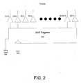
- FIG. 2illustrates an embodiment depicting a block diagram of a gate driver logic.
- a gate driversuch as 106 in FIG. 1 may include a shift register 202 and one or more output buffers 201 a through 201 n.
- One output buffer 201may be used for each row of the active matrix array 107 controlled byte gate driver such as gate driver 106 referenced in FIG. 1 .
- the shift register 202has a data input 204 and a clock input 203 , each of which may operate at any conventional voltage level, such as 5V or 3.3V.
- the output data buffers 201may amplify the output of the shift register 202 .
- the power consumed by the circuitmay be reduced because the shift register 202 does not operate at the higher voltage level required to drive the gates of the TFTs in the active matrix array 107 . This may occur because the shift register 202 encompasses the majority of the circuitry for controlling the gate driver logic.
- FIG. 3illustrates an embodiment depicting a block diagram of the data control logic.
- the data control logicmay include a shift register 306 , a latch 305 , and an output buffer 301 for each column of the active matrix array 107 illustrated in FIG. 1 .
- the shift register 306has a data input 308 and a clock input 302 , each of which may operate at any conventional voltage level, such as 5V or 3.3V.
- datamay be loaded one row at a time into the shift register 306 .
- a data enable line 309may be used to permit the data in the shift register 306 to be passed through the latch 305 to the output buffers 301 .
- the output data buffers 301may amplify the output of the latch 305 .
- the power consumed byte data control logicmay thus be reduced in a manner consistent with the power consumption reduction of the gate control logic described above in reference to FIG. 2 .
- more than one shift registersmay replace the shift register 306 of FIG. 3 .
- the data linesmay be more rapidly loaded with information.
- Such a designmay be used where the refresh cycle of the display is shorter than the write cycle of the active matrix array 107 of FIG. 1 where only a single shift register is used for the data lines.
- multiple shift registersmay be used to enable rapid display updates.
- more than one latchesmay be used to replace the single latch 305 of FIG. 3 where the width of a single latch is less than the number of columns in the active matrix array 107 illustrated in FIG. 1 .
Landscapes
- Engineering & Computer Science (AREA)
- Physics & Mathematics (AREA)
- Computer Hardware Design (AREA)
- General Physics & Mathematics (AREA)
- Theoretical Computer Science (AREA)
- Control Of Indicators Other Than Cathode Ray Tubes (AREA)
Abstract
Description
- This application claims benefit of, under 35 U.S.C. §119(e), U.S. Provisional Application Ser. No. 60/570,938, filed May 13, 2004.
- Disclosed is an electric visual display. More particularly, an electric paper display using a thin film transistor active matrix array and integrated addressing logic to control the output of the display is disclosed useful, for example, as point of purchase signs.
- Traditional signs have been based upon printed materials, paper, plastic, metal, etc., and are, therefore, not programmable. Accordingly, they are not easily changed. In an attempt to overcome this problem, electronically programmable and/or controllable signs have been in existence for many years. For example, liquid crystal diode (LCD) displays, cathode ray tube (CRT) displays, and other electrically-addressable displays will display an image in response to applied electric signals or fields. However, such signs typically require a large amount of electricity, since they must provide illumination in order to be visible to a viewer.
- Electric writeable media, including twisting-cylinder and rotary ball displays, such as those described in U.S. Pat. Nos. 4,126,854 and 4,143,103 to Sheridon, incorporated herein by reference in their entirety, have been developed to overcome the problems with previous programmable signs. Twisting-cylinder displays, rotary-ball displays and related displays have numerous advantages over conventional displays, such as LCDs and CRTs, since they are suitable for viewing in ambient light, they retain an image indefinitely in the absence of an applied electric field, and they can be made to be very lightweight and/or flexible. For further advantages of such displays, see U.S. Pat. No. 5,389,945 to Sheridon, incorporated herein by reference in its entirety. Such displays are referred to herein as “electric paper” displays. An example of such a display is a SmartPaper™ display from Gyricon LLC.
- Another type of electric writeable media is known as an electronic ink display, such as the one described in U.S. Pat. No. 6,518,949 to Drzaic, which is incorporated herein by reference. An electronic ink display includes at least one capsule filled with a plurality of particles, made of a material such as titania, and a dyed suspending fluid. When a direct-current electric field of an appropriate polarity is applied across the capsule, the particles move to a viewed surface of the display and scatter light. When the applied electric field is reversed, the particles move to the rear surface of the display and the viewed surface of the display then appears dark.
- Yet another type of electric writeable media, also described in U.S. Pat. No. 6,518,949 to Drzaic, includes a first set of particles and a second set of particles in a capsule. The first set of particles and the second set of particles have contrasting optical properties, such as contrasting colors, and can have, for example, differing electrophoretic properties. The capsule also contains a substantially clear fluid. The capsule has electrodes disposed adjacent to it connected to a voltage source, which may provide an alternating-current field or a direct-current field to the capsule. Upon application of an electric field across the electrodes, the first set of particles moves toward a first electrode, while the second set of particles moves toward a second electrode. If the electric field is reversed, the first set of particles moves toward the second electrode and the second set of particles moves toward the first electrode. Other examples of writeable media include liquid crystal diode displays, encapsulated electrophoretic displays, and other displays.
- Electric paper displays respond slowly to changes in applied voltage. However, electric paper displays are also generally addressed infrequently. Recent developments in electric paper displays are permitting operation at voltage thresholds of approximately 40V. Current electric displays are driven with crystal silicon integrated circuits in separate packages. Such integrated circuits are costly and increase the size of the display. As a result, new technologies for supplying threshold voltages are being explored.
- A thin film transistor (TFT) active matrix array is composed of an array of TFTs. A TFT is a Metal-Oxide-Semiconductor Field Effect Transistor (MOSFET) implemented using thin film technology. A TFT uses thin films, which may be made of for example, amorphous silicon (a-Si), polycrystalline silicon (p-Si), or which may be an organic material, and a glass substrate. Current flows between the source and drain of a TFT when a voltage is applied to its gate. Thus, by connecting the gate of a TFT to the power rail of the TFT active matrix array, a TFT is turned on (at a positive voltage). If the gate of a TFT is connected to the ground rail, the TFT is turned off (at zero voltage).
- Active matrix liquid crystal displays are a well-established technology. The gate voltage swing is typically from −10 V to +15 V, and the data voltage swing is typically ±10V. However, the transistors are capable of withstanding substantially greater voltages. For example, it is reasonable to expect that a transistor with a gate nitride thickness of 300 nm will have a breakdown voltage of more than 50V. Moreover, threshold voltage shifts that are induced by a high gate voltage are insignificant if the transistor is not turned on for a large percentage of time.
- Addressing logic has previously been constructed for active matrix liquid crystal display arrays. However, such designs require logic to compensate for threshold drifts of critical transistors.
- A need exists for methods and systems of controlling a display that use electric paper and thin film transistor active matrix technologies to provide low power operation and/or pixel-addressability without the need for additional logic to compensate for transistor threshold drifts.
- Aspects disclosed herein include
- an electric display, comprising a plurality of rotatable elements;
- a thin film transistor active matrix array comprising a plurality of thin film transistors arranged as one or more rows and one or more columns, wherein each thin film transistor has a gate input and a data input;
- gate control logic coupled to the gate inputs of the thin film transistors; and
- data control logic coupled to the data inputs of the plurality of transistors, and
- an electric display, comprising a plurality of multichromal media;
- a thin film transistor active matrix array comprising a plurality of thin film transistors arranged as one or more rows and one or more columns, wherein each thin film transistor has a gate input and a data input;
- gate control logic coupled to the gate inputs of the thin film transistors; and
- data control logic coupled to the data inputs of the thin film transistors.
FIG. 1 depicts a block diagram of an exemplary control circuitry for an electric paper display.FIG. 2 depicts a block diagram of an exemplary gate driver logic.FIG. 3 depicts a block diagram of an exemplary data control logic.- In embodiments there is illustrated:
- an electric paper display for use, for example, as a point of purchase sign, comprising a thin film transistor active matrix array and an integrated addressing logic to control the output of the display. In an embodiment, an electric paper display includes a plurality of rotatable elements, a thin film transistor active matrix array which includes a plurality of thin film transistors, gate control logic coupled to the gate inputs of the plurality of transistors, and data control logic coupled to the data inputs of the thin film transistors. The thin film transistors may be arranged as one or more rows and one or more columns of film transistors, for example, at least one row and at least one column of transistors. Furthermore, each transistor may have a gate input and a data input. In an embodiment, the gate control logic includes a shift register and one or more output buffers. Each of the output buffers may be coupled to the shift register. In an embodiment, the data control logic includes a shift register, one or more latches and one or more output buffers. Each of the latches may be coupled to the shift register. Each of the output buffers may be coupled to one of the latches.
- In an embodiment, an electric display includes a plurality of multichromal media, a thin film transistor active matrix array including a plurality of thin film transistors each having a gate input and a data input, gate control logic coupled to the gate inputs of the thin film transistors, and data control logic coupled to the data inputs of the plurality of transistors. The plurality of thin film transistors may be arranged as one or more rows and one or more columns of thin film transistors, for example, at least one row and at least one column of thin film transistors. In an embodiment, the gate control logic includes a shift register and one or more output buffers. Each output buffer may be coupled to the shift register. In an embodiment, the data control logic includes a shift register, one or more latches coupled to the shift register, and one or more output buffers. Each output buffer may be coupled to one of the latches.
- In an embodiment, the electric paper display using a thin film transistor (TFT) active matrix and an integrated addressing logic to control the output of the display is provided, in which a TFT active matrix array is similar to a dynamic random access memory (DRAM) array. In other words, each pixel may be at the intersection of horizontal and vertical address lines and may be addressed by enabling both lines. In one embodiment, when using TFT active matrix arrays with electric paper displays, a localized electric field used to rotate one or more rotatable elements within an electric paper display may be generated from each TFT. A rotatable element may be an anisotropic particle such as, for example, a ball, a cylinder or other particulate matter. The rotatable element may rotate when an electric field is applied across the element while the element is suspended in an electrophoretic substance. As such, an individual TFT may be used as an active switch for each picture element or pixel. Alternatively, multiple TFTs may be used to form a pixel where a first TFT controls rotatable elements of a first color, such as red, a second TFT controls rotatable elements of a second color, such as blue, and a third TFT controls rotatable elements of a third color, such as green. Each sub-pixel TFT may control one or more rotatable elements.
- In an alternative embodiment, other multichromal media may be used in place of or in addition to the rotatable elements described above. Such multichromal media may include inks, dyes, pigments, pigment dispersions, dye solutions, multichromal rotatable elements, and other media that can display two or more colors depending on their orientation with respect to a viewer. Furthermore, multichromal media may include any combination of the above-listed exemplary substances or elements.
- In the application of electric paper to point of purchase signs, the circuitry to control the sign may only be empowered for a very small portion of the day. For example, if a point of purchase sign were updated once a day, the sign may only be powered for about two minutes per day, or for about 0.14% of the time. If a threshold shift were to occur in a TFT during this time because a voltage surpassing the TFT gate breakdown voltage is supplied to the TFT, the TFT would return to its original state during the time that the circuit is not powered. As a result, control circuitry for a TFT active matrix array used in an electric paper display may be simplified by not accounting for voltage levels greater than the TFT gate breakdown voltage.
- Generally, TFT active matrix arrays may be limited by the speed with which they may be updated. Since liquid crystal displays are generally refreshed at 60 Hz, the low mobility of the TFT active matrix array may be unable to provide a complete refresh to a liquid crystal display with a refresh cycle. In addition, as the size of the display increases, the load capacitance and, therefore, the transistor power up time increases as well. In contrast, the addressing speed required for electric paper displays is much slower than for an active matrix liquid crystal display. As a result a TFT active matrix array may be used in an electric paper display to perform the addressing logic of the pixel elements.
- In addition, the control circuitry of an electric paper display would differ from active matrix liquid crystal displays in that the gate and data lines would each require only a two-level output. Although the addressing logic for gate lines in an electric paper display and in a liquid crystal display may be similar, the data lines in a liquid crystal display utilizes a range of output voltages to provide the grayscale capability of an LCD. In contrast, in electric paper displays the data lines may require only two states: on or off. In this embodiment, the circuitry may be vastly simplified.
FIG. 1 illustrates a block diagram of a control circuitry for an electric paper display according to an embodiment. Theelectric paper display 105 includes one or more data drivers, such as the five data drivers shown inFIG. 1 at101a,101b,101c,101dand101e;agate driver 106 and anactive matrix array 107. Each data driver101a-101emay include adata input 108, a shareddata clock 102 and a data enable109, for latching the data input to the output of the data driver. Thegate driver 106 may include agate input 104 and agate clock 103. Thegate driver 106 may have one output for each row of theactive matrix array 107.- Alternate embodiments may include different numbers of data drivers101 ad/or
gate drivers 106. In addition, different voltage levels may be used for the one or more gate drivers. For instance, where a color electric paper display is used, one or more gate drivers may be used for each color used for a pixel. The gate drivers for each sub-pixel color may be driven at different voltage levels so that only the rotatable elements corresponding to an appropriate color are updated at a given time. FIG. 2 illustrates an embodiment depicting a block diagram of a gate driver logic. A gate driver, such as106 inFIG. 1 may include ashift register 202 and one ormore output buffers 201athrough201n.Oneoutput buffer 201 may be used for each row of theactive matrix array 107 controlled byte gate driver such asgate driver 106 referenced inFIG. 1 . Theshift register 202 has adata input 204 and aclock input 203, each of which may operate at any conventional voltage level, such as 5V or 3.3V. The output data buffers201 may amplify the output of theshift register 202. As a result the power consumed by the circuit may be reduced because theshift register 202 does not operate at the higher voltage level required to drive the gates of the TFTs in theactive matrix array 107. This may occur because theshift register 202 encompasses the majority of the circuitry for controlling the gate driver logic.FIG. 3 illustrates an embodiment depicting a block diagram of the data control logic. The data control logic may include ashift register 306, alatch 305, and anoutput buffer 301 for each column of theactive matrix array 107 illustrated inFIG. 1 . Theshift register 306 has adata input 308 and aclock input 302, each of which may operate at any conventional voltage level, such as 5V or 3.3V. In operation, data may be loaded one row at a time into theshift register 306. When a complete row has been enabled, a data enableline 309 may be used to permit the data in theshift register 306 to be passed through thelatch 305 to the output buffers301. The output data buffers301 may amplify the output of thelatch 305. The power consumed byte data control logic may thus be reduced in a manner consistent with the power consumption reduction of the gate control logic described above in reference toFIG. 2 .- In an alternate embodiment, more than one shift registers may replace the
shift register 306 ofFIG. 3 . By using multiple shift registers, the data lines may be more rapidly loaded with information. Such a design may be used where the refresh cycle of the display is shorter than the write cycle of theactive matrix array 107 ofFIG. 1 where only a single shift register is used for the data lines. In addition, for large displays, multiple shift registers may be used to enable rapid display updates. In addition, more than one latches may be used to replace thesingle latch 305 ofFIG. 3 where the width of a single latch is less than the number of columns in theactive matrix array 107 illustrated inFIG. 1 . - It will be appreciated that various of the above-disclosed and other features and functions, or alternatives thereof, may be desirably combined into many other different systems or applications. Also that various presently unforeseen or unanticipated alternatives, modifications, variations or improvements therein may be subsequently made by those skilled in the art which are also intended to be encompassed by the following claims.
Claims (14)
Priority Applications (1)
| Application Number | Priority Date | Filing Date | Title |
|---|---|---|---|
| US11/001,925US20050253803A1 (en) | 2004-05-13 | 2004-12-02 | Electric paper display with a thin film transistor active matrix and integrated addressing logic |
Applications Claiming Priority (2)
| Application Number | Priority Date | Filing Date | Title |
|---|---|---|---|
| US57093804P | 2004-05-13 | 2004-05-13 | |
| US11/001,925US20050253803A1 (en) | 2004-05-13 | 2004-12-02 | Electric paper display with a thin film transistor active matrix and integrated addressing logic |
Publications (1)
| Publication Number | Publication Date |
|---|---|
| US20050253803A1true US20050253803A1 (en) | 2005-11-17 |
Family
ID=35308943
Family Applications (1)
| Application Number | Title | Priority Date | Filing Date |
|---|---|---|---|
| US11/001,925AbandonedUS20050253803A1 (en) | 2004-05-13 | 2004-12-02 | Electric paper display with a thin film transistor active matrix and integrated addressing logic |
Country Status (1)
| Country | Link |
|---|---|
| US (1) | US20050253803A1 (en) |
Cited By (5)
| Publication number | Priority date | Publication date | Assignee | Title |
|---|---|---|---|---|
| US20070002008A1 (en)* | 2005-07-04 | 2007-01-04 | Seiko Epson Corporation | Electro-optical arrangement |
| US8274077B2 (en) | 2005-09-29 | 2012-09-25 | Semiconductor Energy Laboratory Co., Ltd. | Semiconductor device and manufacturing method thereof |
| WO2014079101A1 (en)* | 2012-11-22 | 2014-05-30 | 深圳市华星光电技术有限公司 | Liquid crystal display panel and liquid crystal display device |
| WO2018018883A1 (en)* | 2016-07-25 | 2018-02-01 | 京东方科技集团股份有限公司 | Pixel circuit, display device, display apparatus and driving method |
| US20240290243A1 (en)* | 2023-02-28 | 2024-08-29 | Wuhan Boe Optoelectronics Technology Co., Ltd. | Display panel and driving method therefor, and display device |
Citations (17)
| Publication number | Priority date | Publication date | Assignee | Title |
|---|---|---|---|---|
| US4126854A (en)* | 1976-05-05 | 1978-11-21 | Xerox Corporation | Twisting ball panel display |
| US4143103A (en)* | 1976-05-04 | 1979-03-06 | Xerox Corporation | Method of making a twisting ball panel display |
| US5389945A (en)* | 1989-11-08 | 1995-02-14 | Xerox Corporation | Writing system including paper-like digitally addressed media and addressing device therefor |
| US5936259A (en)* | 1997-10-16 | 1999-08-10 | Lucent Technologies Inc. | Thin film transistor and organic semiconductor material thereof |
| US5981970A (en)* | 1997-03-25 | 1999-11-09 | International Business Machines Corporation | Thin-film field-effect transistor with organic semiconductor requiring low operating voltages |
| US6194837B1 (en)* | 1997-07-02 | 2001-02-27 | Seiko Epson Corporation | Display device with thin film transistor (TFT) and organic semiconductor film in a luminescent element |
| US6265243B1 (en)* | 1999-03-29 | 2001-07-24 | Lucent Technologies Inc. | Process for fabricating organic circuits |
| US20020033792A1 (en)* | 2000-08-31 | 2002-03-21 | Satoshi Inoue | Electrophoretic display |
| US6373453B1 (en)* | 1997-08-21 | 2002-04-16 | Seiko Epson Corporation | Active matrix display |
| US6518949B2 (en)* | 1998-04-10 | 2003-02-11 | E Ink Corporation | Electronic displays using organic-based field effect transistors |
| US20030137521A1 (en)* | 1999-04-30 | 2003-07-24 | E Ink Corporation | Methods for driving bistable electro-optic displays, and apparatus for use therein |
| US20040032637A1 (en)* | 2002-05-29 | 2004-02-19 | Seiko Epson Corporation | Electro-optical device and method of manufacturing the same, element driving device and method of manufacturing the same, element substrate, and electronic apparatus |
| US20040174335A1 (en)* | 2003-03-03 | 2004-09-09 | Lee Wang | Driver control scheme for electronic-ink display |
| US6885146B2 (en)* | 2002-03-14 | 2005-04-26 | Semiconductor Energy Laboratory Co., Ltd. | Display device comprising substrates, contrast medium and barrier layers between contrast medium and each of substrates |
| US20050104816A1 (en)* | 2003-10-28 | 2005-05-19 | Seiko Epson Corporation | Method for driving electro-optical device, electro-optical device and electronic equipment |
| US7023418B2 (en)* | 2000-07-18 | 2006-04-04 | Matsushita Electric Industrial Co., Ltd. | Display device, electronic paper and electronic paper file |
| US20060209058A1 (en)* | 2003-04-02 | 2006-09-21 | Tetsurou Nakamura | Display |
- 2004
- 2004-12-02USUS11/001,925patent/US20050253803A1/ennot_activeAbandoned
Patent Citations (18)
| Publication number | Priority date | Publication date | Assignee | Title |
|---|---|---|---|---|
| US4143103A (en)* | 1976-05-04 | 1979-03-06 | Xerox Corporation | Method of making a twisting ball panel display |
| US4126854A (en)* | 1976-05-05 | 1978-11-21 | Xerox Corporation | Twisting ball panel display |
| US5389945A (en)* | 1989-11-08 | 1995-02-14 | Xerox Corporation | Writing system including paper-like digitally addressed media and addressing device therefor |
| US5981970A (en)* | 1997-03-25 | 1999-11-09 | International Business Machines Corporation | Thin-film field-effect transistor with organic semiconductor requiring low operating voltages |
| US6194837B1 (en)* | 1997-07-02 | 2001-02-27 | Seiko Epson Corporation | Display device with thin film transistor (TFT) and organic semiconductor film in a luminescent element |
| US6373453B1 (en)* | 1997-08-21 | 2002-04-16 | Seiko Epson Corporation | Active matrix display |
| US5936259A (en)* | 1997-10-16 | 1999-08-10 | Lucent Technologies Inc. | Thin film transistor and organic semiconductor material thereof |
| US6518949B2 (en)* | 1998-04-10 | 2003-02-11 | E Ink Corporation | Electronic displays using organic-based field effect transistors |
| US6265243B1 (en)* | 1999-03-29 | 2001-07-24 | Lucent Technologies Inc. | Process for fabricating organic circuits |
| US6551717B2 (en)* | 1999-03-29 | 2003-04-22 | Lucent Technologies Inc. | Process for fabricating organic circuits |
| US20030137521A1 (en)* | 1999-04-30 | 2003-07-24 | E Ink Corporation | Methods for driving bistable electro-optic displays, and apparatus for use therein |
| US7023418B2 (en)* | 2000-07-18 | 2006-04-04 | Matsushita Electric Industrial Co., Ltd. | Display device, electronic paper and electronic paper file |
| US20020033792A1 (en)* | 2000-08-31 | 2002-03-21 | Satoshi Inoue | Electrophoretic display |
| US6885146B2 (en)* | 2002-03-14 | 2005-04-26 | Semiconductor Energy Laboratory Co., Ltd. | Display device comprising substrates, contrast medium and barrier layers between contrast medium and each of substrates |
| US20040032637A1 (en)* | 2002-05-29 | 2004-02-19 | Seiko Epson Corporation | Electro-optical device and method of manufacturing the same, element driving device and method of manufacturing the same, element substrate, and electronic apparatus |
| US20040174335A1 (en)* | 2003-03-03 | 2004-09-09 | Lee Wang | Driver control scheme for electronic-ink display |
| US20060209058A1 (en)* | 2003-04-02 | 2006-09-21 | Tetsurou Nakamura | Display |
| US20050104816A1 (en)* | 2003-10-28 | 2005-05-19 | Seiko Epson Corporation | Method for driving electro-optical device, electro-optical device and electronic equipment |
Cited By (13)
| Publication number | Priority date | Publication date | Assignee | Title |
|---|---|---|---|---|
| US20070002008A1 (en)* | 2005-07-04 | 2007-01-04 | Seiko Epson Corporation | Electro-optical arrangement |
| US8790959B2 (en) | 2005-09-29 | 2014-07-29 | Semiconductor Energy Laboratory Co., Ltd. | Semiconductor device and manufacturing method thereof |
| US8466463B2 (en) | 2005-09-29 | 2013-06-18 | Semiconductor Energy Laboratory Co., Ltd. | Semiconductor device and manufacturing method thereof |
| US8629069B2 (en) | 2005-09-29 | 2014-01-14 | Semiconductor Energy Laboratory Co., Ltd. | Semiconductor device and manufacturing method thereof |
| US8669550B2 (en) | 2005-09-29 | 2014-03-11 | Semiconductor Energy Laboratory Co., Ltd. | Semiconductor device and manufacturing method thereof |
| US8274077B2 (en) | 2005-09-29 | 2012-09-25 | Semiconductor Energy Laboratory Co., Ltd. | Semiconductor device and manufacturing method thereof |
| US8796069B2 (en) | 2005-09-29 | 2014-08-05 | Semiconductor Energy Laboratory Co., Ltd. | Semiconductor device and manufacturing method thereof |
| US10304962B2 (en) | 2005-09-29 | 2019-05-28 | Semiconductor Energy Laboratory Co., Ltd. | Semiconductor device and manufacturing method thereof |
| US12183832B2 (en) | 2005-09-29 | 2024-12-31 | Semiconductor Energy Laboratory Co., Ltd. | Semiconductor device and manufacturing method thereof |
| WO2014079101A1 (en)* | 2012-11-22 | 2014-05-30 | 深圳市华星光电技术有限公司 | Liquid crystal display panel and liquid crystal display device |
| WO2018018883A1 (en)* | 2016-07-25 | 2018-02-01 | 京东方科技集团股份有限公司 | Pixel circuit, display device, display apparatus and driving method |
| US10482834B2 (en) | 2016-07-25 | 2019-11-19 | Boe Technology Group Co., Ltd. | Pixel circuit, display device, display apparatus and driving method |
| US20240290243A1 (en)* | 2023-02-28 | 2024-08-29 | Wuhan Boe Optoelectronics Technology Co., Ltd. | Display panel and driving method therefor, and display device |
Similar Documents
| Publication | Publication Date | Title |
|---|---|---|
| CN1892803B (en) | Electro-optical device | |
| KR100830106B1 (en) | Electrophoretic device and method of driving the same | |
| US8004490B2 (en) | Active-matrix bistable display device | |
| US20160225321A1 (en) | Electro-optic displays with reduced remnant voltage, and related apparatus and methods | |
| US20070057905A1 (en) | Electrophoretic display activation with blanking frames | |
| KR101838047B1 (en) | Electrophoresis display device and driving method the same | |
| US20080018589A1 (en) | Drive Apparatus for Bistable Displayer and Method Thereof | |
| WO2001091096A1 (en) | Display and recorded medium | |
| US8284156B2 (en) | Electrophoretic display device employing organic thin film transistors, driving method for driving circuits of the electrophoretic display device, and electronic apparatus including the electrophoretic display device | |
| WO2018128040A1 (en) | Display device and driving method | |
| KR20050049547A (en) | Electrophoretic display device | |
| CN116110334A (en) | Display device and data driving circuit | |
| WO2007135594A1 (en) | Electrophoretic display devices | |
| CN102376284B (en) | Electro-optical device and electronic equipment | |
| US20090160759A1 (en) | Moving particle display device | |
| JP4115099B2 (en) | Display device | |
| US20050253803A1 (en) | Electric paper display with a thin film transistor active matrix and integrated addressing logic | |
| JP3863729B2 (en) | Display device | |
| KR102866288B1 (en) | Methods for driving electro-optical displays | |
| US11580919B2 (en) | Driving method of display device | |
| KR100923349B1 (en) | Ferroelectric Liquid Crystal Display | |
| KR20070058071A (en) | How to operate electrophoretic display panel | |
| KR20080034544A (en) | Electrophoresis display |
Legal Events
| Date | Code | Title | Description |
|---|---|---|---|
| AS | Assignment | Owner name:JP MORGAN CHASE BANK,TEXAS Free format text:SECURITY AGREEMENT;ASSIGNOR:XEROX CORPORATION;REEL/FRAME:016761/0158 Effective date:20030625 Owner name:JP MORGAN CHASE BANK, TEXAS Free format text:SECURITY AGREEMENT;ASSIGNOR:XEROX CORPORATION;REEL/FRAME:016761/0158 Effective date:20030625 | |
| AS | Assignment | Owner name:XEROX CORPORATION, CONNECTICUT Free format text:ASSIGNMENT OF ASSIGNORS INTEREST;ASSIGNORS:THOMPSON, MALCOLM;MARTIN, RUSSEL;REEL/FRAME:016468/0724;SIGNING DATES FROM 20040517 TO 20041129 | |
| STCB | Information on status: application discontinuation | Free format text:ABANDONED -- FAILURE TO RESPOND TO AN OFFICE ACTION | |
| AS | Assignment | Owner name:XEROX CORPORATION, CONNECTICUT Free format text:RELEASE BY SECURED PARTY;ASSIGNOR:JPMORGAN CHASE BANK, N.A. AS SUCCESSOR-IN-INTEREST ADMINISTRATIVE AGENT AND COLLATERAL AGENT TO BANK ONE, N.A.;REEL/FRAME:061360/0628 Effective date:20220822 |