US20050253307A1 - Method of patterning a conductive layer on a substrate - Google Patents
Method of patterning a conductive layer on a substrateDownload PDFInfo
- Publication number
- US20050253307A1 US20050253307A1US10/843,194US84319404AUS2005253307A1US 20050253307 A1US20050253307 A1US 20050253307A1US 84319404 AUS84319404 AUS 84319404AUS 2005253307 A1US2005253307 A1US 2005253307A1
- Authority
- US
- United States
- Prior art keywords
- layer
- conductive
- recited
- polymerizable
- forming
- Prior art date
- Legal status (The legal status is an assumption and is not a legal conclusion. Google has not performed a legal analysis and makes no representation as to the accuracy of the status listed.)
- Abandoned
Links
- 238000000034methodMethods0.000titleclaimsabstractdescription50
- 239000000758substrateSubstances0.000titleclaimsabstractdescription41
- 238000000059patterningMethods0.000titleclaimsabstractdescription6
- 239000007788liquidSubstances0.000claimsabstractdescription15
- 239000000203mixtureSubstances0.000claimsdescription53
- 230000005855radiationEffects0.000claimsdescription53
- 239000000463materialSubstances0.000claimsdescription51
- 238000004528spin coatingMethods0.000claimsdescription13
- OKTJSMMVPCPJKN-UHFFFAOYSA-NCarbonChemical compound[C]OKTJSMMVPCPJKN-UHFFFAOYSA-N0.000claimsdescription6
- 235000019241carbon blackNutrition0.000claimsdescription6
- 239000006229carbon blackSubstances0.000claimsdescription6
- 238000000151depositionMethods0.000claimsdescription6
- 239000002861polymer materialSubstances0.000claimsdescription6
- 229910002804graphiteInorganic materials0.000claimsdescription5
- 239000010439graphiteSubstances0.000claimsdescription5
- 239000012530fluidSubstances0.000claims10
- 238000006116polymerization reactionMethods0.000claims1
- 238000007711solidificationMethods0.000abstract1
- 230000008023solidificationEffects0.000abstract1
- 239000010410layerSubstances0.000description136
- 239000004020conductorSubstances0.000description27
- 239000002904solventSubstances0.000description18
- 238000010606normalizationMethods0.000description17
- 238000010521absorption reactionMethods0.000description15
- -1but not limited toPolymers0.000description12
- 230000008569processEffects0.000description12
- 229920002050silicone resinPolymers0.000description12
- 229920001296polysiloxanePolymers0.000description11
- XUIMIQQOPSSXEZ-UHFFFAOYSA-NSiliconChemical compound[Si]XUIMIQQOPSSXEZ-UHFFFAOYSA-N0.000description9
- 238000000576coating methodMethods0.000description9
- 229910052710siliconInorganic materials0.000description9
- 239000010703siliconSubstances0.000description9
- 239000004094surface-active agentSubstances0.000description9
- 239000003431cross linking reagentSubstances0.000description8
- 239000003054catalystSubstances0.000description7
- 239000011248coating agentSubstances0.000description7
- 238000001723curingMethods0.000description7
- 230000015572biosynthetic processEffects0.000description6
- 230000003287optical effectEffects0.000description6
- LBLYYCQCTBFVLH-UHFFFAOYSA-N2-Methylbenzenesulfonic acidChemical compoundCC1=CC=CC=C1S(O)(=O)=OLBLYYCQCTBFVLH-UHFFFAOYSA-N0.000description5
- BNCADMBVWNPPIZ-UHFFFAOYSA-N2-n,2-n,4-n,4-n,6-n,6-n-hexakis(methoxymethyl)-1,3,5-triazine-2,4,6-triamineChemical compoundCOCN(COC)C1=NC(N(COC)COC)=NC(N(COC)COC)=N1BNCADMBVWNPPIZ-UHFFFAOYSA-N0.000description5
- YCKRFDGAMUMZLT-UHFFFAOYSA-NFluorine atomChemical compound[F]YCKRFDGAMUMZLT-UHFFFAOYSA-N0.000description5
- 238000004132cross linkingMethods0.000description5
- 230000008021depositionEffects0.000description5
- 238000001914filtrationMethods0.000description5
- 229910052731fluorineInorganic materials0.000description5
- 239000011737fluorineSubstances0.000description5
- CATSNJVOTSVZJV-UHFFFAOYSA-Nheptan-2-oneChemical compoundCCCCCC(C)=OCATSNJVOTSVZJV-UHFFFAOYSA-N0.000description5
- 229910052751metalInorganic materials0.000description5
- 239000002184metalSubstances0.000description5
- 229920006037cross link polymerPolymers0.000description4
- KUDUQBURMYMBIJ-UHFFFAOYSA-Nethylene glycol diacrylateSubstancesC=CC(=O)OCCOC(=O)C=CKUDUQBURMYMBIJ-UHFFFAOYSA-N0.000description4
- 238000001465metallisationMethods0.000description4
- BPSIOYPQMFLKFR-UHFFFAOYSA-Ntrimethoxy-[3-(oxiran-2-ylmethoxy)propyl]silaneChemical compoundCO[Si](OC)(OC)CCCOCC1CO1BPSIOYPQMFLKFR-UHFFFAOYSA-N0.000description4
- PSGCQDPCAWOCSH-UHFFFAOYSA-N(4,7,7-trimethyl-3-bicyclo[2.2.1]heptanyl) prop-2-enoateChemical compoundC1CC2(C)C(OC(=O)C=C)CC1C2(C)CPSGCQDPCAWOCSH-UHFFFAOYSA-N0.000description3
- 239000000654additiveSubstances0.000description3
- 230000000996additive effectEffects0.000description3
- 238000004891communicationMethods0.000description3
- 229920001577copolymerPolymers0.000description3
- 230000009969flowable effectEffects0.000description3
- 230000009477glass transitionEffects0.000description3
- 238000004519manufacturing processMethods0.000description3
- 238000005240physical vapour depositionMethods0.000description3
- 125000006850spacer groupChemical group0.000description3
- 238000012876topographyMethods0.000description3
- VYZAMTAEIAYCRO-UHFFFAOYSA-NChromiumChemical compound[Cr]VYZAMTAEIAYCRO-UHFFFAOYSA-N0.000description2
- RTZKZFJDLAIYFH-UHFFFAOYSA-NDiethyl etherChemical compoundCCOCCRTZKZFJDLAIYFH-UHFFFAOYSA-N0.000description2
- LYCAIKOWRPUZTN-UHFFFAOYSA-NEthylene glycolChemical compoundOCCOLYCAIKOWRPUZTN-UHFFFAOYSA-N0.000description2
- PXHVJJICTQNCMI-UHFFFAOYSA-NNickelChemical compound[Ni]PXHVJJICTQNCMI-UHFFFAOYSA-N0.000description2
- BLRPTPMANUNPDV-UHFFFAOYSA-NSilaneChemical compound[SiH4]BLRPTPMANUNPDV-UHFFFAOYSA-N0.000description2
- VYPSYNLAJGMNEJ-UHFFFAOYSA-NSilicium dioxideChemical compoundO=[Si]=OVYPSYNLAJGMNEJ-UHFFFAOYSA-N0.000description2
- 238000000231atomic layer depositionMethods0.000description2
- 230000009286beneficial effectEffects0.000description2
- 238000005229chemical vapour depositionMethods0.000description2
- 229910052804chromiumInorganic materials0.000description2
- 239000011651chromiumSubstances0.000description2
- 230000000295complement effectEffects0.000description2
- 150000001875compoundsChemical class0.000description2
- 238000006482condensation reactionMethods0.000description2
- 230000001419dependent effectEffects0.000description2
- 238000005137deposition processMethods0.000description2
- 238000010438heat treatmentMethods0.000description2
- 230000002209hydrophobic effectEffects0.000description2
- 239000003999initiatorSubstances0.000description2
- CWQXQMHSOZUFJS-UHFFFAOYSA-Nmolybdenum disulfideChemical compoundS=[Mo]=SCWQXQMHSOZUFJS-UHFFFAOYSA-N0.000description2
- 229910052982molybdenum disulfideInorganic materials0.000description2
- 229920000620organic polymerPolymers0.000description2
- 125000005375organosiloxane groupChemical group0.000description2
- 238000011160researchMethods0.000description2
- 229910000077silaneInorganic materials0.000description2
- 230000007480spreadingEffects0.000description2
- 238000003892spreadingMethods0.000description2
- 238000012546transferMethods0.000description2
- OXBLVCZKDOZZOJ-UHFFFAOYSA-N2,3-DihydrothiopheneChemical compoundC1CC=CS1OXBLVCZKDOZZOJ-UHFFFAOYSA-N0.000description1
- XMLYCEVDHLAQEL-UHFFFAOYSA-N2-hydroxy-2-methyl-1-phenylpropan-1-oneChemical compoundCC(C)(O)C(=O)C1=CC=CC=C1XMLYCEVDHLAQEL-UHFFFAOYSA-N0.000description1
- QTBSBXVTEAMEQO-UHFFFAOYSA-MAcetateChemical compoundCC([O-])=OQTBSBXVTEAMEQO-UHFFFAOYSA-M0.000description1
- NIXOWILDQLNWCW-UHFFFAOYSA-MAcrylateChemical compound[O-]C(=O)C=CNIXOWILDQLNWCW-UHFFFAOYSA-M0.000description1
- LSNNMFCWUKXFEE-UHFFFAOYSA-MBisulfiteChemical compoundOS([O-])=OLSNNMFCWUKXFEE-UHFFFAOYSA-M0.000description1
- 229920003270Cymel®Polymers0.000description1
- 239000004593EpoxySubstances0.000description1
- LFQSCWFLJHTTHZ-UHFFFAOYSA-NEthanolChemical compoundCCOLFQSCWFLJHTTHZ-UHFFFAOYSA-N0.000description1
- 206010073306Exposure to radiationDiseases0.000description1
- XPDWGBQVDMORPB-UHFFFAOYSA-NFluoroformChemical compoundFC(F)FXPDWGBQVDMORPB-UHFFFAOYSA-N0.000description1
- 229920000265PolyparaphenylenePolymers0.000description1
- 208000034809Product contaminationDiseases0.000description1
- 239000006087Silane Coupling AgentSubstances0.000description1
- 150000007513acidsChemical class0.000description1
- 125000000217alkyl groupChemical group0.000description1
- 229910052782aluminiumInorganic materials0.000description1
- XAGFODPZIPBFFR-UHFFFAOYSA-NaluminiumChemical compound[Al]XAGFODPZIPBFFR-UHFFFAOYSA-N0.000description1
- 229920003180amino resinPolymers0.000description1
- 125000003118aryl groupChemical group0.000description1
- 239000005388borosilicate glassSubstances0.000description1
- 238000005219brazingMethods0.000description1
- 239000006227byproductSubstances0.000description1
- 229910052799carbonInorganic materials0.000description1
- 238000006243chemical reactionMethods0.000description1
- 229920001940conductive polymerPolymers0.000description1
- 229920000547conjugated polymerPolymers0.000description1
- 238000013461designMethods0.000description1
- 239000003989dielectric materialSubstances0.000description1
- MTHSVFCYNBDYFN-UHFFFAOYSA-Ndiethylene glycolChemical compoundOCCOCCOMTHSVFCYNBDYFN-UHFFFAOYSA-N0.000description1
- KPUWHANPEXNPJT-UHFFFAOYSA-NdisiloxaneChemical class[SiH3]O[SiH3]KPUWHANPEXNPJT-UHFFFAOYSA-N0.000description1
- 230000009977dual effectEffects0.000description1
- 150000002148estersChemical class0.000description1
- 230000008020evaporationEffects0.000description1
- 238000001704evaporationMethods0.000description1
- 230000005284excitationEffects0.000description1
- 239000000945fillerSubstances0.000description1
- 125000001153fluoro groupChemical groupF*0.000description1
- 229920002313fluoropolymerPolymers0.000description1
- 239000005350fused silica glassSubstances0.000description1
- 239000000499gelSubstances0.000description1
- 229910052736halogenInorganic materials0.000description1
- 150000002366halogen compoundsChemical class0.000description1
- 150000002367halogensChemical class0.000description1
- LNMQRPPRQDGUDR-UHFFFAOYSA-Nhexyl prop-2-enoateChemical compoundCCCCCCOC(=O)C=CLNMQRPPRQDGUDR-UHFFFAOYSA-N0.000description1
- MVPKCNRIHYSCCY-UHFFFAOYSA-Nhydroxy-dimethyl-[3-(oxiran-2-ylmethoxy)propyl]silaneChemical compoundC[Si](C)(O)CCCOCC1CO1MVPKCNRIHYSCCY-UHFFFAOYSA-N0.000description1
- WGCNASOHLSPBMP-UHFFFAOYSA-NhydroxyacetaldehydeNatural productsOCC=OWGCNASOHLSPBMP-UHFFFAOYSA-N0.000description1
- 238000002329infrared spectrumMethods0.000description1
- 150000002500ionsChemical class0.000description1
- 150000002576ketonesChemical class0.000description1
- 238000001459lithographyMethods0.000description1
- 230000007246mechanismEffects0.000description1
- JDSHMPZPIAZGSV-UHFFFAOYSA-NmelamineChemical compoundNC1=NC(N)=NC(N)=N1JDSHMPZPIAZGSV-UHFFFAOYSA-N0.000description1
- QSHDDOUJBYECFT-UHFFFAOYSA-NmercuryChemical compound[Hg]QSHDDOUJBYECFT-UHFFFAOYSA-N0.000description1
- 229910052753mercuryInorganic materials0.000description1
- 125000002496methyl groupChemical group[H]C([H])([H])*0.000description1
- 238000004377microelectronicMethods0.000description1
- 238000012986modificationMethods0.000description1
- 230000004048modificationEffects0.000description1
- 238000001127nanoimprint lithographyMethods0.000description1
- 229910052759nickelInorganic materials0.000description1
- 239000011368organic materialSubstances0.000description1
- 238000012856packingMethods0.000description1
- 239000012071phaseSubstances0.000description1
- 125000001997phenyl groupChemical group[H]C1=C([H])C([H])=C(*)C([H])=C1[H]0.000description1
- 229920003209poly(hydridosilsesquioxane)Polymers0.000description1
- 229920000553poly(phenylenevinylene)Polymers0.000description1
- 229920000767polyanilinePolymers0.000description1
- 229920000642polymerPolymers0.000description1
- 229920000193polymethacrylatePolymers0.000description1
- 239000002243precursorSubstances0.000description1
- 238000012545processingMethods0.000description1
- 125000001436propyl groupChemical group[H]C([*])([H])C([H])([H])C([H])([H])[H]0.000description1
- 239000010453quartzSubstances0.000description1
- 229920005989resinPolymers0.000description1
- 239000011347resinSubstances0.000description1
- 230000004044responseEffects0.000description1
- 150000004756silanesChemical class0.000description1
- 239000002356single layerSubstances0.000description1
- 239000007787solidSubstances0.000description1
- 239000007790solid phaseSubstances0.000description1
- 239000003381stabilizerSubstances0.000description1
- 239000000126substanceSubstances0.000description1
- 230000008961swellingEffects0.000description1
- 238000001029thermal curingMethods0.000description1
- 229920001187thermosetting polymerPolymers0.000description1
- QTSIIQWGUWMBTD-UHFFFAOYSA-Ntrihydroxy-[3-(oxiran-2-ylmethoxy)propyl]silaneChemical compoundO[Si](O)(O)CCCOCC1CO1QTSIIQWGUWMBTD-UHFFFAOYSA-N0.000description1
- LFBULLRGNLZJAF-UHFFFAOYSA-Ntrimethoxy(oxiran-2-ylmethoxymethyl)silaneChemical compoundCO[Si](OC)(OC)COCC1CO1LFBULLRGNLZJAF-UHFFFAOYSA-N0.000description1
- NCLFWRGBSGFNNA-UHFFFAOYSA-Ntrimethoxy-(3-methyloxiran-2-yl)silaneChemical compoundCO[Si](OC)(OC)C1OC1CNCLFWRGBSGFNNA-UHFFFAOYSA-N0.000description1
- 238000002211ultraviolet spectrumMethods0.000description1
Images


Classifications
- G—PHYSICS
- G03—PHOTOGRAPHY; CINEMATOGRAPHY; ANALOGOUS TECHNIQUES USING WAVES OTHER THAN OPTICAL WAVES; ELECTROGRAPHY; HOLOGRAPHY
- G03F—PHOTOMECHANICAL PRODUCTION OF TEXTURED OR PATTERNED SURFACES, e.g. FOR PRINTING, FOR PROCESSING OF SEMICONDUCTOR DEVICES; MATERIALS THEREFOR; ORIGINALS THEREFOR; APPARATUS SPECIALLY ADAPTED THEREFOR
- G03F7/00—Photomechanical, e.g. photolithographic, production of textured or patterned surfaces, e.g. printing surfaces; Materials therefor, e.g. comprising photoresists; Apparatus specially adapted therefor
- G03F7/0002—Lithographic processes using patterning methods other than those involving the exposure to radiation, e.g. by stamping
- B—PERFORMING OPERATIONS; TRANSPORTING
- B82—NANOTECHNOLOGY
- B82Y—SPECIFIC USES OR APPLICATIONS OF NANOSTRUCTURES; MEASUREMENT OR ANALYSIS OF NANOSTRUCTURES; MANUFACTURE OR TREATMENT OF NANOSTRUCTURES
- B82Y10/00—Nanotechnology for information processing, storage or transmission, e.g. quantum computing or single electron logic
- B—PERFORMING OPERATIONS; TRANSPORTING
- B82—NANOTECHNOLOGY
- B82Y—SPECIFIC USES OR APPLICATIONS OF NANOSTRUCTURES; MEASUREMENT OR ANALYSIS OF NANOSTRUCTURES; MANUFACTURE OR TREATMENT OF NANOSTRUCTURES
- B82Y40/00—Manufacture or treatment of nanostructures
Definitions
- the field of inventionrelates generally to micro-fabrication of structures. More particularly, the present invention is directed to a method for creating positive tone structures employing imprint lithography.
- single level metallizationhas proved desirable where device density is not a constraint, for example, in the manufacture of large displays.
- the simplicity of the single level metallization and reduced cost of manufacture devices employing the samemakes single level metallization a desired design characteristic when forming certain integrated circuits.
- the present inventionincludes a method of forming a patterned conductive layer on a substrate that features creating a multi-layered structure by solidifying a liquid layer to have a pattern including electrically insulative protrusions and recessions, defining a dielectric patterned layer. Formed upon the dielectric patterned layer is an electrically conductive liquid conformal layer. The electrically conductive liquid conformal layer is solidified to form a solidified electrically conductive conformal layer. Portions of the solidified electrically conductive conformal layer are removed to expose regions thereof. The regions are electrically insulated from adjacent regions of the solidified conductive conformal layer by one of the protrusions.
- the pattern of the electrically conductive layeris a function of, if not defined by, the electrically insulative protrusions and recession of the dielectric patterned layer. As a result, a single level layer of high density multiple conductive elements may be fabricated.
- FIG. 1is a perspective view of a lithographic system in accordance with the present invention
- FIG. 2is a simplified elevation view of a lithographic system, shown in FIG. 1 , employed to create a patterned imprinting layer in accordance with the present invention
- FIG. 3is a simplified representation of material from which a patterned imprinting layer, shown in FIG. 2 , is comprised before being polymerized and cross-linked in accordance with the present invention
- FIG. 4is a simplified representation of cross-linked polymer material into which the material shown in FIG. 3 is transformed after being subjected to radiation in accordance with the present invention
- FIG. 5is a simplified elevation view of an imprint device spaced-apart from the patterned imprinting layer, shown in FIG. 1 , after patterning in accordance with the present invention
- FIG. 6is a simplified elevation view of formation of a multi-layered structure on a solidified imprinting layer, shown in FIG. 5 , by deposition of a conformal layer, adjacent to the patterned imprinting layer, employing a mold in accordance with one embodiment of the present invention;
- FIG. 7is a simplified elevation view after a blanket etch of the multi-layered structure, shown in FIG. 6 , to form a crown surface in the conformal layer with portions of the patterned imprinting layer being exposed in accordance with one embodiment of the present invention
- FIG. 8is a simplified elevation view showing formation of a planarization layer in accordance with an alternate embodiment of the present invention.
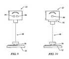
- FIG. 9is a simplified plan view of a radiation source employed in the lithographic system shown in FIG. 1 , depicting dual radiation sources;
- FIG. 10is a simplified plan view of a radiation source employed in the lithographic system, shown in FIG. 1 , depicting single radiation source;
- FIG. 11is a cross-sectional view of a substrate shown in FIGS. 1, 2 , 5 , 6 , 7 and 8 , showing an infra-red absorption layer in accordance with the present invention
- FIG. 12is a cross-sectional view of a substrate shown in FIGS. 1, 2 , 5 , 6 , 7 and 8 , showing an infra-red absorption layer in accordance with an alternate embodiment of the present invention
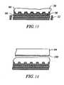
- FIG. 13is a cross-sectional view showing a release layer and a planarization layer that may be employed in accordance with the present invention.
- FIG. 14is a cross-sectional view showing a release layer applied to a planarization mold shown in FIG. 12 .
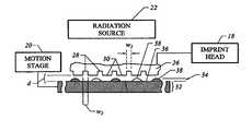
- FIG. 1depicts a lithographic system 10 in accordance with one embodiment of the present invention that includes a pair of spaced-apart bridge supports 12 having a bridge 14 and a stage support 16 extending therebetween. Bridge 14 and stage support 16 are spaced-apart. Coupled to bridge 14 is an imprint head 18 , which extends from bridge 14 toward stage support 16 . Disposed upon stage support 16 to face imprint head 18 is a motion stage 20 . Motion stage 20 is configured to move with respect to stage support 16 along X- and Y-axes and may provide movement along the Z-axis as well.
- a radiation source 22is coupled to system 10 to impinge actinic radiation upon motion stage 20 . As shown, radiation source 22 is coupled to bridge 14 and includes a power generator 23 connected to radiation source 22 .
- Patterned mold 26includes a plurality of features defined by a plurality of spaced-apart recesses 28 and projections 30 . Projections 30 have a width W 1 , and recesses 28 have a width W 2 , both of which are measured in a direction that extends transversely to the Z axis.
- the plurality of featuresdefines an original pattern that forms the basis of a pattern to be transferred into a substrate 32 positioned on motion stage 20 .
- imprint head 18is adapted to move along the Z-axis and to vary a distance “d” between patterned mold 26 and substrate 32 .
- motion stage 20may move template 24 along the Z-axis.
- the features on patterned mold 26may be imprinted into a flowable region of substrate 32 , discussed more fully below.
- Radiation source 22is located so that patterned mold 26 is positioned between radiation source 22 and substrate 32 .
- patterned mold 26is fabricated from material that allows it to be substantially transparent to the radiation produced by radiation source 22 .
- An exemplary systemis available under the trade name IMPRIO 100TM from Molecular Imprints, Inc. having a place of business at 1807-C Braker Lane, Suite 100, Austin, Tex. 78758. The system description for the IMPRIO 100TM is available at www.molecularimprints.com and is incorporated herein by reference.
- a flowable regionsuch as an imprinting layer 34 , is disposed on a portion of surface 36 that presents a substantially planar profile.
- the flowable regionis deposited as a plurality of spaced-apart discrete droplets 38 of a material 40 on substrate 32 , discussed more fully below.
- Material 40is substantially silicon-free and may be selectively polymerized and cross-linked to record an inverse of the original pattern therein, defining a recorded pattern.
- Material 40is shown in FIG. 4 as being cross-linked at points 42 , forming cross-linked polymer material 44 .
- the pattern recorded in imprinting layer 34is produced, in part, by mechanical contact with patterned mold 26 .
- the distance “d”is reduced to allow imprinting layer 34 to come into mechanical contact with patterned mold 26 , spreading droplets 38 so as to form imprinting layer 34 with a contiguous formation of material 40 over surface 36 .
- distance “d”is reduced to allow sub-portions 46 of imprinting layer 34 to ingress into and fill recesses 28 .
- sub-portions 48 of imprinting layer 34 in superimposition with projections 30remain after the desired, usually minimum distance “d,” has been reached, leaving sub-portions 46 with a thickness t, and sub-portions 48 with a thickness t 2 .
- Thickness t 2is referred to as a residual thickness.
- Thicknesses “t 1 “and “t 2 ”may be any thickness desired, dependent upon the application.
- the total volume contained in droplets 38may be such so as to minimize, or to avoid, a quantity of material 40 from extending beyond the region of surface 36 in superimposition with patterned mold 26 , while obtaining desired thicknesses t 1 and t 2 .
- radiation source 22produces actinic radiation that polymerizes and cross-links material 40 , forming cross-linked polymer material 44 .
- the composition of imprinting layer 34transforms from material 40 to material 44 , which is a solid.
- material 44is solidified to form solidified imprinting layer 134 with a side having a shape that conforms to a shape of a surface 50 of patterned mold 26 , shown more clearly in FIG. 5 .
- solidified imprinting layer 134is formed having recessions 52 and protrusions 54 .
- step and repeat processAn exemplary step and repeat process is disclosed in published U.S. patent application No. 2004/0008334, which is assigned to the assignee of the present invention and is incorporated by reference herein.
- the characteristics of material 40are important to efficiently pattern substrate 32 in light of the unique deposition process employed.
- material 40is deposited on substrate 32 as a plurality of discrete and spaced-apart droplets 38 .
- the combined volume of droplets 38is such that the material 40 is distributed appropriately over an area of surface 36 where imprinting layer 34 is to be formed.
- the total volume of imprinting material 40 in droplets 38defines the distance “d” to be obtained so that the total volume occupied by material 40 in the gap defined between patterned mold 26 and the portion of substrate 32 in superimposition therewith once the desired distance “d” is reached is substantially equal to the total volume of material 40 in droplets 38 .
- imprinting layer 34is spread and patterned concurrently with the pattern being subsequently set by exposure to radiation, such as ultraviolet radiation.
- radiationsuch as ultraviolet radiation.
- material 40have certain characteristics to provide rapid and even spreading of material 40 in droplets 38 over surface 36 so that the all thicknesses t 1 are substantially uniform and all residual thicknesses t 2 are substantially uniform.
- An exemplary composition for material 40is silicon-free and consists of the following:
- COMPOSITION 1isobornyl acrylate comprises approximately 55% of the composition, n-hexyl acrylate comprises approximately 27%, ethylene glycol diacrylate comprises approximately 15% and the initiator 2-hydroxy-2-methyl-1-phenyl-propan-1-one comprises approximately 3%.
- the initiatoris sold under the trade name DAROCUR® 1173 by CIBA® of Tarrytown, N.Y.
- the above-identified compositionalso includes stabilizers that are well known in the chemical art to increase the operational life of the composition.
- COMPOSITION 1may be employed with a template treated to have a mold surface that is hydrophobic and/or low surface energy, e.g., an a priori release layer.
- an additivemay be included in COMPOSITION 1.
- material 40may include, as an additive, a surfactant.
- a surfactantis defined as any molecule, one tail of which is hydrophobic.
- Surfactantsmay be either fluorine-containing, e.g., include a fluorine chain, or may not include any fluorine in the surfactant molecule structure.
- An exemplary surfactantis available under the trade name ZONYL® FSO-100 from DUPONTTM that has a general structure of R 1 R 2 , where R 1 ⁇ F(CF 2 CF 2 ) Y with y being in a range of 1 to 7 , inclusive, and R 2 ⁇ CH 2 CH 2 O(CH 2 CH 2 O) X H where X is in a range of 0 to 15, inclusive.
- ZONYL® FSO-100from DUPONTTM that has a general structure of R 1 R 2 , where R 1 ⁇ F(CF 2 CF 2 ) Y with y being in a range of 1 to 7 , inclusive, and R 2 ⁇ CH 2 CH 2 O(CH 2 CH 2 O) X H where X is in a range of 0 to 15, inclusive.
- the ZONYL® FSO-100 additivecomprises less than 1% of the composition with the relative amounts of the remaining components being as discussed above with respect to COMPOSITION 1. However, the percentage of ZONYL® FSO-100 may be greater than 1%.
- COMPOSITIONS 1 and 2are electrically non-conductive, i.e., COMPOSITIONS 1 and 2 are dielectric materials. As a result, COMPOSITIONS 1 and 2 may be employed to form a single level metallized device. Specifically, by forming solidified imprinting layer 134 with a desired pattern, solidified imprinting layer 134 an electrically conductive layer may be disposed adjacent to solidified imprinting layer 134 . In this manner, a desired single level electrical circuit may be formed.
- COMPOSITIONS 1 and 2may be doped with a conductive component, such as carbon-black and graphite, to form a conductive material.
- COMPOSITIONS 1 and 2may be formed from, or doped with, a conductive polymer including, but not limited to, organic polymers, copolymers, and conjugated polymers, such as poly(para-phenylene), polyaniline, and poly(p-phenylenevinylene).
- the conductive materialwould be employed to form a multi-layered structure 56 by forming a conductive conformal layer 58 adjacent to solidified imprinting layer 134 .
- the conductive materialmay be deposited adjacent to solidified imprinting layer 134 using any known technique to form conformal layer 58 , such as the technique discussed above with respect to deposition of material 40 .
- the conductive materialmay be deposited adjacent to solidified imprinting layer 134 employing spin-coating techniques, discussed more fully below.
- planarization mold 126has a substantially smooth, if not planar, surface 150 .
- Surface 150contacts droplets 38 , causing the same to spread in a manner discussed above, excepting that conformal layer 58 is formed having a smooth, if not substantially planar, surface referred to as a normalization surface 62 .
- the shape of normalization surface 62matches the profile of surface 150 .
- planarization mold 126is an optical flat that has sufficient area to concurrently planarize all regions of substrate 32 that includes conductive material employed to form conformal layer 58 .
- conformal layer 58includes first and second opposed sides.
- First side 60faces imprinting layer 134 and has a profile complementary to the profile of the imprinting layer 134 .
- the second sidefaces away from imprinting layer 134 , forming normalization surface 62 .
- a blanket etchis employed to remove portions of conformal layer 58 to provide multi-layered structure 56 with a crown surface 70 .
- the blanket etchmay be achieved in a system available from LAM Research 9400 SE obtained from Lam Research, Inc. of Fremont, Calif.
- normalization surface 62is subjected to an isotropic halogen reactive ion etch (“RIE”) rich in fluorine, i.e., wherein at least one of the precursors was a fluorine-containing material, for example, and without limitation, a combination of CHF 3 and O 2 .
- RIEisotropic halogen reactive ion etch
- Other suitable halogen compoundsinclude, for example, and without limitation, CF 4 .
- Normalization surface 62is subjected to the blanket etch sufficient to expose crown surface 70 .
- Crown surface 70is defined by an exposed surface 72 of each of electrically insulative protrusions 54 and upper surfaces of electrically conductive portions 74 that remain on conformal layer 58 after the blanket etch.
- the composition of conformal layer 58is such that when the blanket etch is applied to conformal layer 58 , crown surface 70 is provided with a substantially planar profile. That is, the thickness of protrusions 54 , shown as “a”, is substantially the same as the thickness of portions 74 , shown as “b”.
- An exemplary blanket etchmay be a plasma etch process employing a fluorine-based chemistry. In this manner, single level circuits may be formed consisting of electrically conductive portions 74 separated by electrically insulative protrusions 54 .
- exemplary material that may be employed to form conformal layer 158includes a silicon-containing composition that is doped with a conductive material, such as polyanyline, carbon black and graphite.
- a silicon-containing compositionincludes a silicone resin, a cross-linking agent, a catalyst, and a solvent.
- the silicone resinis process compatible, satisfying ionic, purity, and by-product contamination requirements desired.
- the cross-linking agentis included to cross-link the silicone resin, providing conformal layer 158 with the properties to record a pattern thereon having very small feature sizes, i.e., on the order of a few nanometers.
- the catalystis provided to produce a condensation reaction in response to thermal energy, e.g., heat, causing the silicone resin and the cross-linking agent to polymerize and to cross-link, forming a cross-linked polymer material.
- the solvent selectedis compatible with the silicone resin and represents the remaining balance of the conductive material. It is desired that the solvent minimize, if not avoid, causing distortions in solidified imprinting layer 134 due, for example, to swelling of solidified imprinting layer 134 .
- the silicone resincan be any alkyl and/or aryl substituted polysiloxane, copolymer, blend or mixture thereof.
- a silicone resininclude ultraviolet (UV) curable sol-gels; UV curable epoxy silicone; UV curable acrylate silicone; and UV curable silicone via thiolene chemistry; and non-cured materials, such as hydrogen silsesquioxanes; and poly(meth)acrylate/siloxane copolymers.
- a hydroxyl-functional polysiloxaneis used, such as a hydroxyl-functional organo-siloxane, with examples of organo-siloxanes including methyl, phenyl, propyl and their mixtures.
- the silicone resinmay be present in the conductive composition in amounts of approximately 2% to 40% by weight, depending on the thicknesses desired for conformal layer 158 .
- An exemplary example of a hydroxyl-functional polysiloxane used in the present inventionis a silicon T-resin intermediate available from Dow Corning® (Midland, Mich.) under the trade name Z-6018.
- the cross-linking agentis a compound that includes two or more polymerizable groups.
- the cross-linking agentmay be present in the conductive composition in amounts of approximately 2% to 50% by weight in relation to the quantity of silicone resin present. Typically, the cross-linking agent is present in the conductive composition in an amount of approximately 20% to 30%.
- An exemplary example of a cross-linking agent used in the present inventionis a hexamethoxymethylmelamine(HMMM)-based aminoplast cross-linking agent available from Cytec Industries, Inc. (West Paterson, N.J.) under the trade name CYMEL 303ULF.
- the catalystmay be any component that catalyzes a condensation reaction. Suitable catalysts may include, but are not limited to, acidic compounds, such as sulfonic acid.
- the catalystmay be present in the conductive material in amounts of approximately 0.05% to 5% by weight in relation to the silicone resin present. Typically, the catalyst is present in the conductive material in an amount of approximately 1% to 2%.
- An exemplary example of a catalyst used in the present inventionis toluenesulfonic acid available from Cytec Industries, Inc. (West Paterson, N.J.) under the trade name CYCAT 4040.
- a solventis utilized.
- the solventcan be any solvent or combination of solvents that satisfies several criteria. As mentioned above, the solvent should not cause solidified imprinting layer 134 to swell. In addition, the evaporation rate of the solvent should be established so that a desired quantity of the solvent evaporates as a result of the spin-coating process, while providing sufficient viscosity to facilitate planarization of the conductive material in furtherance of forming conformal layer 158 .
- Suitable solventsmay include, but are not limited to, alcohol, ether, a glycol or glycol ether, a ketone, an ester, an acetate and mixtures thereof.
- the solventmay be present in the conductive material used to form conformal layer 158 in amounts of approximately 60% to 98% by weight, dependent upon the desired thicknesses of conformal layer 158 .
- An exemplary example of a solvent used in the present inventionis methyl amyl ketone available from Aldrich Co. (St. Louis, Mo.) under the trade name MAK.
- the composition of conformal layer 158is altered to include an epoxy-functional silane coupling agent to improve the cross-linking reaction and to improve the rate of cross-linking.
- epoxy-functional silanesmay include glycidoxymethyltrimethoxysilane, 3-glycidoxypropyltrihydroxysilane, 3-glycidoxypropyldimethylhydroxysilane, 3-glycidoxypropyltrimeth oxysilane, 2,3-epoxypropyltrimethoxysilane, and the like.
- the epoxy-functional silanemay be present in conformal layer 158 in amounts of approximately 2% to 30% by weight of conductive compound in relation to the silicone resin and typically in an amount of 5% to 10%.
- An exemplary example of epoxy-functional silane used in the present inventionis gamma-glycidoxypropyltrimethoxysilane available from GE Silicone/OSi Specialty (Wilton, Conn.) under the trade name A187.
- compositions from which to form conformal layer 158are as follows:
- hydroxyl-functional polysiloxanecomprises approximately 4% of the composition, hexamethoxymethylmelamine comprisies approximately 0.95%, toluenesulfonic acid comprises approximately 0.05% and methyl amyl ketone comprises approximately 95%.
- hydroxyl-functional polysiloxanecomprises approximately 4% of the composition, hexamethoxymethylmelamine comprisies approximately 0.7%, gamma-glycidoxypropyltrimethoxysilane comprisies approximately 0.25%, toluenesulfonic acid comprises approximately 0.05%, and methyl amyl ketone comprises approximately 95%.
- Both COMPOSITIONS 3 and 4are made up of at least 4% of the silicone resin. Upon curing, however, the quantity of silicon present in conformal layer 158 is at least 5% by weight and typically in a range of 20% or greater. Specifically, the quantity and the composition of the solvent present in COMPOSITIONS 3 and 4 are selected so that a substantial portion of the solvent evaporates during spin-coating application of the COMPOSITION 3 or 4 on solidified imprinting layer 134 . In the present exemplary conductive material, approximately 90% of the solvent evaporates during spin-coating. Upon exposing the conductive material to thermal energy, the remaining 10% of the solvent evaporates, leaving conformal layer 158 with approximately 20% silicon by weight.
- An exemplary method of forming conformal layer 158includes spinning-on approximately 4 mL of the conductive material deposited proximate to a center of solidified imprinting layer 134 .
- substrate 32is spun at 1000 rev/min for 1 min by placing substrate 32 on a hot plate.
- the conductive materialis subjected to thermal energy by baking at 150° C. for 1 min.
- the aforementioned spin-coating and curing processesare simply repeated.
- the solvent employedis selected so as not to remove, “wash away,” the conductive material in a well-cured conformal layer 158 .
- the spin-coating and curing processesprovide conformal layer 158 first and second opposed sides.
- First side 160faces imprinting layer 134 and has a profile complementary to the profile of imprinting layer 134 .
- the second sidefaces away from imprinting layer 134 forming normalization surface 162 , which is substantially smooth and typically planar and without necessitating implementation of planarization mold 126 .
- normalization surface 162provides solidified conformal layer 158 with a substantially normalized profile. It is believed that normalization surface 162 is provided with a smooth, e.g., substantially planar, topography by ensuring that COMPOSITIONS 3 and 4 have a glass transition temperature lower than the curing temperature.
- the temperature difference between the glass transition temperature and the curing temperaturebe sufficient to allow the conductive material to reflow during curing to maximize smoothness, e.g., planarity of normalization surface 162 , in a minimum amount of time.
- the COMPOSITIONS 3 and 4each have a glass transition temperature of approximately 50° C. and a curing temperature of 150° C.
- the distances k 2 , k 4 , k 6 , k 8 and k 10 between apex 64 of each of protrusions 54 and normalization surface 162are substantially the same.
- the distances k 1 , k 3 , k 5 , k 7 , k 9 and k 11 between nadir surface 66 of each of recessions 52 and normalization surface 162are substantially the same.
- the silicon-containing conductive materialmay be deposited as a plurality of droplets as discussed above with respect to forming conformal layer 58 , or may be spun-on.
- planarization mold 126is employed to further planarize normalization surface 162 . Thereafter, the silicon-containing conductive material is solidified and planarized mold 126 is separated from conformal layer 158 . Thereafter, conformal layer 158 is processed as discussed above to form single level circuits.
- radiation source 22may be selected to provide actinic radiation to effectuate cross-linking using both infrared (IR) radiation and ultraviolet radiation.
- An exemplary radiation source 22may include multiple sources, each of which produces a single range of wavelengths of radiation, and is shown including two radiation sources 84 and 86 .
- Radiation source 84may be any known in the art capable of producing IR radiation
- radiation source 86may be any known in the art capable of producing actinic radiation employed to polymerize and to cross-link material in droplets 38 , such as UV radiation.
- a circuit(not shown) is in electrical communication with radiation sources 84 and 86 to selectively allow radiation in the UV and IR spectra to impinge upon substrate 32 .
- radiation source 22may include a single radiation source that produces multiple ranges of wavelength, which may be selectively controlled to impinge upon substrate 32 sequentially or concurrently.
- An exemplary radiation source 22consists of a single broad spectrum radiation source 90 that produces UV and IR radiation, which may consist of a mercury (Hg) lamp.
- a filtering system 92is utilized to selectively impinge differing types of radiation upon substrate 32 .
- Filtering system 92comprises a high pass filter (not shown) and a low pass filter (not shown), each in optical communication with radiation source 90 .
- Filtering system 92may position the high pass filter (not shown) such that optical path 88 comprises IR radiation or filtering system 92 may position the low pass filter (not shown) such that optical path 88 comprises UV radiation.
- the high pass and low pass filters (not shown)may be any known in the art, such as interference filters comprising two semi-reflective coatings with a spacer disposed therebetween. The index of refraction and the thickness of the spacer determine the frequency band being selected and transmitted through the interference filter. Therefore, the appropriate index of refraction and thickness of the spacer is chosen for both the high pass filter (not shown) and the low pass filter (not shown), such that the high pass filter (not shown) permits passage of IR radiation and the low pass filter (not shown) permits passage of UV radiation.
- a processor(not shown) is in data communication with radiation source 90 and filtering system 92 to selectively allow the desired wavelength of radiation to propagate along optical path 88 .
- the circuitenables high pass filter (not shown) when IR radiation is desired and enables the low pass filter (not shown) when UV radiation is desired.
- substrate 32may have one or more existing layers disposed thereon before deposition of imprinting layer 34 .
- heating the conductive materialmay be problematic because the material from which the wafer is formed and/or the preexisting layers on the wafer, e.g., solidified imprinting layer 134 , are substantially non-responsive to infrared radiation. As a result, very little energy transfer may occur, resulting in it being difficult to raise the temperature of the conductive material sufficient to achieve cross-linking.
- one of the layers included with substrate 32may be an infrared absorption layer 94 .
- Absorption layer 94comprises a material that is excited when exposed to IR radiation and produces a localized heat source.
- absorption layer 94is formed from a material that maintains a constant phase state during the heating process, which may include a solid phase state. Specifically, the IR radiation impinging upon absorption layer 94 causes an excitation of the molecules contained therein, generating heat.
- absorption layer 94The heat generated in absorption layer 94 is transferred to the conductive material via conduction through the wafer and/or any intervening layer of material thereon, e.g., absorption layer 94 may be disposed on surface 36 so as to be disposed between substrate 32 and solidified imprinting layer 134 .
- absorption layer 94 and substrate 32provide a bifurcated heat transfer mechanism that is able to absorb IR radiation and to produce a localized heat source sensed by the conductive material in one of conformal layers 58 and 158 . In this manner, absorption layer 94 creates a localized heat source on surface 36 .
- absorption layer 94may be deposited using any known technique, including spin-coating, chemical vapor deposition, physical vapor deposition, atomic layer deposition and the like.
- Exemplary materialsmay be formed from a carbon-based PVD coating, organic thermo set coating with carbon black filler or molybdenum disulfide (MoS 2 ) based coating.
- absorption layer 94may be disposed on a side of substrate 32 disposed opposite to solidified imprinting layer 134 . As a result, absorption layer 94 may be permanently or removably attached. Exemplary materials that may be employed as absorption layer 94 include black nickel and anodized black aluminum. Also, black chromium may be employed as absorption layer 94 . Black chromium is typically deposited as a mixture of oxides and is used as a coating for solar cells.
- patterned mold 26may be fabricated from any material, such as, but not limited to, fused-silica, quartz, silicon, organic polymers, siloxane polymers, borosilicate glass, fluorocarbon polymers, metal, and combinations of the above.
- the actinic radiationpropagates through patterned mold 26 . Therefore, it is desired that patterned mold 26 be fabricated from material that is substantially transparent to the actinic radiation.
- the plurality of features on patterned mold 26are shown as recesses 28 extending along a direction parallel to projections 30 that provide a cross-section of patterned mold 26 with a shape of a battlement.
- recesses 28 and projections 30may correspond to virtually any feature required to create an integrated circuit and may be as small as a few tenths of nanometers.
- Primer layer 96may be formed upon substrate 32 .
- Primer layer 96has proved beneficial when surface 36 of substrate 32 appears rough when compared to the features' dimensions to be formed in imprinting layer 34 . Additionally, it has been found beneficial to deposit primer layer 96 when forming imprinting layer 34 upon a previously disposed patterned layer present on substrate 32 .
- Primer layer 96may also functions, inter alia, to provide a standard interface with imprinting layer 34 , thereby reducing the need to customize each process to the material from which substrate 32 is formed.
- primer layer 96may be formed from an organic material with the same etch characteristics as imprinting layer 34 .
- Primer layer 96is fabricated in such a manner so as to possess a continuous, smooth, relatively defect-free surface that may exhibit excellent adhesion to imprinting layer 34 .
- An exemplary material to use to form primer layer 96is available from Brewer Science, Inc. of Rolla, Mo. under the trade name DUV30J-6.
- surface 50may be treated with a low surface energy coating 98 .
- Low surface energy coating 98may be applied using any known process.
- processing techniquesmay include chemical vapor deposition method, physical vapor deposition, atomic layer deposition or various other techniques, brazing and the like.
- a low surface energy coating 198may be applied to planarization mold 126 , shown in FIG. 14 .
- the surfactanthas a surface energy associated therewith that is lower than a surface energy of the polymerizable material in the layer.
Landscapes
- Engineering & Computer Science (AREA)
- Nanotechnology (AREA)
- Chemical & Material Sciences (AREA)
- Physics & Mathematics (AREA)
- General Physics & Mathematics (AREA)
- Crystallography & Structural Chemistry (AREA)
- Theoretical Computer Science (AREA)
- Condensed Matter Physics & Semiconductors (AREA)
- Mathematical Physics (AREA)
- Manufacturing & Machinery (AREA)
- Exposure Of Semiconductors, Excluding Electron Or Ion Beam Exposure (AREA)
- Internal Circuitry In Semiconductor Integrated Circuit Devices (AREA)
- Shaping Of Tube Ends By Bending Or Straightening (AREA)
Abstract
Description
- The field of invention relates generally to micro-fabrication of structures. More particularly, the present invention is directed to a method for creating positive tone structures employing imprint lithography.
- The earliest integrated circuits required a limited number of devices having dimensions that are large by present day standards, typically necessitating only a single layer of metal. Moreover, the pitch of the metal pattern did not limit the device packing density of the integrated circuit. As the devices became smaller and the number of devices employed in a circuit became greater, metal patterns of the integrated circuit limited the device density. These problems were overcome, in large part, by forming multi-level metal patterns.
- However, single level metallization has proved desirable where device density is not a constraint, for example, in the manufacture of large displays. The simplicity of the single level metallization and reduced cost of manufacture devices employing the same makes single level metallization a desired design characteristic when forming certain integrated circuits.
- It is desired, therefore, to provide an improved method for forming circuits from single level metallization.
- The present invention includes a method of forming a patterned conductive layer on a substrate that features creating a multi-layered structure by solidifying a liquid layer to have a pattern including electrically insulative protrusions and recessions, defining a dielectric patterned layer. Formed upon the dielectric patterned layer is an electrically conductive liquid conformal layer. The electrically conductive liquid conformal layer is solidified to form a solidified electrically conductive conformal layer. Portions of the solidified electrically conductive conformal layer are removed to expose regions thereof. The regions are electrically insulated from adjacent regions of the solidified conductive conformal layer by one of the protrusions. The pattern of the electrically conductive layer is a function of, if not defined by, the electrically insulative protrusions and recession of the dielectric patterned layer. As a result, a single level layer of high density multiple conductive elements may be fabricated. These and other embodiments are discussed more fully below.
FIG. 1 is a perspective view of a lithographic system in accordance with the present invention;FIG. 2 is a simplified elevation view of a lithographic system, shown inFIG. 1 , employed to create a patterned imprinting layer in accordance with the present invention;FIG. 3 is a simplified representation of material from which a patterned imprinting layer, shown inFIG. 2 , is comprised before being polymerized and cross-linked in accordance with the present invention;FIG. 4 is a simplified representation of cross-linked polymer material into which the material shown inFIG. 3 is transformed after being subjected to radiation in accordance with the present invention;FIG. 5 is a simplified elevation view of an imprint device spaced-apart from the patterned imprinting layer, shown inFIG. 1 , after patterning in accordance with the present invention;FIG. 6 is a simplified elevation view of formation of a multi-layered structure on a solidified imprinting layer, shown inFIG. 5 , by deposition of a conformal layer, adjacent to the patterned imprinting layer, employing a mold in accordance with one embodiment of the present invention;FIG. 7 is a simplified elevation view after a blanket etch of the multi-layered structure, shown inFIG. 6 , to form a crown surface in the conformal layer with portions of the patterned imprinting layer being exposed in accordance with one embodiment of the present invention;FIG. 8 is a simplified elevation view showing formation of a planarization layer in accordance with an alternate embodiment of the present invention;FIG. 9 is a simplified plan view of a radiation source employed in the lithographic system shown inFIG. 1 , depicting dual radiation sources;FIG. 10 is a simplified plan view of a radiation source employed in the lithographic system, shown inFIG. 1 , depicting single radiation source;FIG. 11 is a cross-sectional view of a substrate shown inFIGS. 1, 2 ,5,6,7 and8, showing an infra-red absorption layer in accordance with the present invention;FIG. 12 is a cross-sectional view of a substrate shown inFIGS. 1, 2 ,5,6,7 and8, showing an infra-red absorption layer in accordance with an alternate embodiment of the present invention;FIG. 13 is a cross-sectional view showing a release layer and a planarization layer that may be employed in accordance with the present invention; andFIG. 14 is a cross-sectional view showing a release layer applied to a planarization mold shown inFIG. 12 .FIG. 1 depicts alithographic system 10 in accordance with one embodiment of the present invention that includes a pair of spaced-apart bridge supports12 having abridge 14 and astage support 16 extending therebetween.Bridge 14 andstage support 16 are spaced-apart. Coupled tobridge 14 is animprint head 18, which extends frombridge 14 towardstage support 16. Disposed uponstage support 16 to faceimprint head 18 is amotion stage 20.Motion stage 20 is configured to move with respect tostage support 16 along X- and Y-axes and may provide movement along the Z-axis as well. Aradiation source 22 is coupled tosystem 10 to impinge actinic radiation uponmotion stage 20. As shown,radiation source 22 is coupled tobridge 14 and includes apower generator 23 connected toradiation source 22.- Referring to both
FIGS. 1 and 2 , connected toimprint head 18 is atemplate 24 having a patternedmold 26 thereon. Anexemplary template 24 is shown in U.S. Pat. No. 6,696,220. Patternedmold 26 includes a plurality of features defined by a plurality of spaced-apart recesses 28 andprojections 30.Projections 30 have a width W1, andrecesses 28 have a width W2, both of which are measured in a direction that extends transversely to the Z axis. The plurality of features defines an original pattern that forms the basis of a pattern to be transferred into asubstrate 32 positioned onmotion stage 20. To that end,imprint head 18 is adapted to move along the Z-axis and to vary a distance “d” between patternedmold 26 andsubstrate 32. Alternatively, or in conjunction withimprint head 18,motion stage 20 may movetemplate 24 along the Z-axis. In this manner, the features on patternedmold 26 may be imprinted into a flowable region ofsubstrate 32, discussed more fully below.Radiation source 22 is located so that patternedmold 26 is positioned betweenradiation source 22 andsubstrate 32. As a result, patternedmold 26 is fabricated from material that allows it to be substantially transparent to the radiation produced byradiation source 22. An exemplary system is available under the trade name IMPRIO 100™ from Molecular Imprints, Inc. having a place of business at 1807-C Braker Lane, Suite 100, Austin, Tex. 78758. The system description for the IMPRIO 100™ is available at www.molecularimprints.com and is incorporated herein by reference. - Referring to both
FIGS. 2 and 3 , a flowable region, such as animprinting layer 34, is disposed on a portion ofsurface 36 that presents a substantially planar profile. In the present embodiment, the flowable region is deposited as a plurality of spaced-apartdiscrete droplets 38 of amaterial 40 onsubstrate 32, discussed more fully below.Material 40 is substantially silicon-free and may be selectively polymerized and cross-linked to record an inverse of the original pattern therein, defining a recorded pattern.Material 40 is shown inFIG. 4 as being cross-linked atpoints 42, formingcross-linked polymer material 44. - Referring to
FIGS. 2, 3 and5, the pattern recorded inimprinting layer 34 is produced, in part, by mechanical contact with patternedmold 26. To that end, the distance “d” is reduced to allowimprinting layer 34 to come into mechanical contact with patternedmold 26, spreadingdroplets 38 so as to formimprinting layer 34 with a contiguous formation ofmaterial 40 oversurface 36. In one embodiment, distance “d” is reduced to allowsub-portions 46 ofimprinting layer 34 to ingress into and fillrecesses 28. - In the present embodiment,
sub-portions 48 ofimprinting layer 34 in superimposition withprojections 30 remain after the desired, usually minimum distance “d,” has been reached, leavingsub-portions 46 with a thickness t, andsub-portions 48 with a thickness t2. Thickness t2is referred to as a residual thickness. Thicknesses “t1“and “t2” may be any thickness desired, dependent upon the application. The total volume contained indroplets 38 may be such so as to minimize, or to avoid, a quantity ofmaterial 40 from extending beyond the region ofsurface 36 in superimposition with patternedmold 26, while obtaining desired thicknesses t1and t2. - Referring to
FIGS. 2, 3 , and4, after a desired distance “d” has been reached,radiation source 22 produces actinic radiation that polymerizes andcross-links material 40, formingcross-linked polymer material 44. As a result, the composition ofimprinting layer 34 transforms frommaterial 40 tomaterial 44, which is a solid. Specifically,material 44 is solidified to form solidifiedimprinting layer 134 with a side having a shape that conforms to a shape of asurface 50 of patternedmold 26, shown more clearly inFIG. 5 . As a result, solidifiedimprinting layer 134 is formed havingrecessions 52 andprotrusions 54. After formation of solidifiedimprinting layer 134, distance “d” is increased so that patternedmold 26 and solidifiedimprinting layer 134 are spaced-apart. Typically, this process is repeated several times to pattern different regions (not shown) ofsubstrate 32, referred to as a step and repeat process. An exemplary step and repeat process is disclosed in published U.S. patent application No. 2004/0008334, which is assigned to the assignee of the present invention and is incorporated by reference herein. - Referring to
FIGS. 1, 2 and3, the characteristics ofmaterial 40 are important to efficientlypattern substrate 32 in light of the unique deposition process employed. As mentioned above,material 40 is deposited onsubstrate 32 as a plurality of discrete and spaced-apartdroplets 38. The combined volume ofdroplets 38 is such that thematerial 40 is distributed appropriately over an area ofsurface 36 whereimprinting layer 34 is to be formed. In this fashion, the total volume of imprintingmaterial 40 indroplets 38 defines the distance “d” to be obtained so that the total volume occupied bymaterial 40 in the gap defined between patternedmold 26 and the portion ofsubstrate 32 in superimposition therewith once the desired distance “d” is reached is substantially equal to the total volume ofmaterial 40 indroplets 38. As a result,imprinting layer 34 is spread and patterned concurrently with the pattern being subsequently set by exposure to radiation, such as ultraviolet radiation. To facilitate the deposition process, it is desired thatmaterial 40 have certain characteristics to provide rapid and even spreading ofmaterial 40 indroplets 38 oversurface 36 so that the all thicknesses t1are substantially uniform and all residual thicknesses t2are substantially uniform. - An exemplary composition for
material 40 is silicon-free and consists of the following: - In COMPOSITION 1, isobornyl acrylate comprises approximately 55% of the composition, n-hexyl acrylate comprises approximately 27%, ethylene glycol diacrylate comprises approximately 15% and the initiator 2-hydroxy-2-methyl-1-phenyl-propan-1-one comprises approximately 3%. The initiator is sold under the trade name DAROCUR® 1173 by CIBA® of Tarrytown, N.Y. The above-identified composition also includes stabilizers that are well known in the chemical art to increase the operational life of the composition. To provide suitable release properties, COMPOSITION 1 may be employed with a template treated to have a mold surface that is hydrophobic and/or low surface energy, e.g., an a priori release layer.
- Referring to
FIGS. 3 and 5 , to improve the release properties of patternedmold 26 and solidifiedimprinting layer 134 and to ensure that solidifiedimprinting layer 134 does not adhere to patternedmold 26, an additive may be included in COMPOSITION 1. To that end,material 40 may include, as an additive, a surfactant. For purposes of this invention a surfactant is defined as any molecule, one tail of which is hydrophobic. Surfactants may be either fluorine-containing, e.g., include a fluorine chain, or may not include any fluorine in the surfactant molecule structure. An exemplary surfactant is available under the trade name ZONYL® FSO-100 from DUPONT™ that has a general structure of R1R2, where R1═F(CF2CF2)Ywith y being in a range of1 to7, inclusive, and R2═CH2CH2O(CH2CH2O)XH where X is in a range of 0 to 15, inclusive. This providesmaterial 40 with the following composition: - The ZONYL® FSO-100 additive comprises less than 1% of the composition with the relative amounts of the remaining components being as discussed above with respect to COMPOSITION 1. However, the percentage of ZONYL® FSO-100 may be greater than 1%.
- Each of COMPOSITIONS 1 and 2 are electrically non-conductive, i.e., COMPOSITIONS 1 and 2 are dielectric materials. As a result, COMPOSITIONS 1 and 2 may be employed to form a single level metallized device. Specifically, by forming solidified
imprinting layer 134 with a desired pattern, solidifiedimprinting layer 134 an electrically conductive layer may be disposed adjacent to solidifiedimprinting layer 134. In this manner, a desired single level electrical circuit may be formed. - Referring to
FIG. 5 , COMPOSITIONS 1 and 2 may be doped with a conductive component, such as carbon-black and graphite, to form a conductive material. In a further embodiment COMPOSITIONS 1 and 2 may be formed from, or doped with, a conductive polymer including, but not limited to, organic polymers, copolymers, and conjugated polymers, such as poly(para-phenylene), polyaniline, and poly(p-phenylenevinylene). The conductive material would be employed to form amulti-layered structure 56 by forming a conductiveconformal layer 58 adjacent to solidifiedimprinting layer 134. Specifically, the conductive material may be deposited adjacent to solidifiedimprinting layer 134 using any known technique to formconformal layer 58, such as the technique discussed above with respect to deposition ofmaterial 40. Alternatively, the conductive material may be deposited adjacent to solidifiedimprinting layer 134 employing spin-coating techniques, discussed more fully below. - Referring to both
FIGS. 2 and 6 , when deposition occurs employing the techniques discussed above, patternedmold 26 is replaced with aplanarization mold 126.Planarization mold 126 has a substantially smooth, if not planar,surface 150.Surface 150contacts droplets 38, causing the same to spread in a manner discussed above, excepting thatconformal layer 58 is formed having a smooth, if not substantially planar, surface referred to as anormalization surface 62. The shape ofnormalization surface 62 matches the profile ofsurface 150. Typically,planarization mold 126 is an optical flat that has sufficient area to concurrently planarize all regions ofsubstrate 32 that includes conductive material employed to formconformal layer 58. Thereafter, the conductive material inconformal layer 58 is solidified andplanarization mold 126 is separated fromconformal layer 58. In this manner,conformal layer 58 includes first and second opposed sides.First side 60 facesimprinting layer 134 and has a profile complementary to the profile of theimprinting layer 134. The second side faces away fromimprinting layer 134, formingnormalization surface 62. - As a result of the topography of
normalization surface 62, distances k2, k4, k6, k8and k10between the apex64 of each ofprotrusions 54 andnormalization surface 62 are substantially the same. Similarly, the distances k1, k3, k5, k7, k9and k11between anadir surface 66 of each ofrecessions 52 andnormalization surface 62 are substantially the same. - Referring to
FIGS. 6 and 7 , after formation ofnormalization surface 62, a blanket etch is employed to remove portions ofconformal layer 58 to providemulti-layered structure 56 with acrown surface 70. For example and without limitation, the blanket etch may be achieved in a system available from LAM Research9400SE obtained from Lam Research, Inc. of Fremont, Calif. In this manner,normalization surface 62 is subjected to an isotropic halogen reactive ion etch (“RIE”) rich in fluorine, i.e., wherein at least one of the precursors was a fluorine-containing material, for example, and without limitation, a combination of CHF3and O2. Other suitable halogen compounds include, for example, and without limitation, CF4.Normalization surface 62 is subjected to the blanket etch sufficient to exposecrown surface 70. Crown surface 70 is defined by an exposedsurface 72 of each of electrically insulativeprotrusions 54 and upper surfaces of electricallyconductive portions 74 that remain onconformal layer 58 after the blanket etch. The composition ofconformal layer 58 is such that when the blanket etch is applied toconformal layer 58,crown surface 70 is provided with a substantially planar profile. That is, the thickness ofprotrusions 54, shown as “a”, is substantially the same as the thickness ofportions 74, shown as “b”. An exemplary blanket etch may be a plasma etch process employing a fluorine-based chemistry. In this manner, single level circuits may be formed consisting of electricallyconductive portions 74 separated by electrically insulativeprotrusions 54.- Referring to
FIGS. 6 and 9 , as discussed above, single level circuits may be formed by formation ofconformal layer 58 employing spin-on and thermal curing techniques. To that end, exemplary material that may be employed to formconformal layer 158 includes a silicon-containing composition that is doped with a conductive material, such as polyanyline, carbon black and graphite. An exemplary silicon-containing composition includes a silicone resin, a cross-linking agent, a catalyst, and a solvent. - The silicone resin is process compatible, satisfying ionic, purity, and by-product contamination requirements desired. The cross-linking agent is included to cross-link the silicone resin, providing
conformal layer 158 with the properties to record a pattern thereon having very small feature sizes, i.e., on the order of a few nanometers. To that end, the catalyst is provided to produce a condensation reaction in response to thermal energy, e.g., heat, causing the silicone resin and the cross-linking agent to polymerize and to cross-link, forming a cross-linked polymer material. The solvent selected is compatible with the silicone resin and represents the remaining balance of the conductive material. It is desired that the solvent minimize, if not avoid, causing distortions in solidifiedimprinting layer 134 due, for example, to swelling of solidifiedimprinting layer 134. - The silicone resin can be any alkyl and/or aryl substituted polysiloxane, copolymer, blend or mixture thereof. Examples of a silicone resin include ultraviolet (UV) curable sol-gels; UV curable epoxy silicone; UV curable acrylate silicone; and UV curable silicone via thiolene chemistry; and non-cured materials, such as hydrogen silsesquioxanes; and poly(meth)acrylate/siloxane copolymers. Preferably, a hydroxyl-functional polysiloxane is used, such as a hydroxyl-functional organo-siloxane, with examples of organo-siloxanes including methyl, phenyl, propyl and their mixtures. The silicone resin may be present in the conductive composition in amounts of approximately 2% to 40% by weight, depending on the thicknesses desired for
conformal layer 158. An exemplary example of a hydroxyl-functional polysiloxane used in the present invention is a silicon T-resin intermediate available from Dow Corning® (Midland, Mich.) under the trade name Z-6018. - The cross-linking agent is a compound that includes two or more polymerizable groups. The cross-linking agent may be present in the conductive composition in amounts of approximately 2% to 50% by weight in relation to the quantity of silicone resin present. Typically, the cross-linking agent is present in the conductive composition in an amount of approximately 20% to 30%. An exemplary example of a cross-linking agent used in the present invention is a hexamethoxymethylmelamine(HMMM)-based aminoplast cross-linking agent available from Cytec Industries, Inc. (West Paterson, N.J.) under the trade name CYMEL 303ULF.
- The catalyst may be any component that catalyzes a condensation reaction. Suitable catalysts may include, but are not limited to, acidic compounds, such as sulfonic acid. The catalyst may be present in the conductive material in amounts of approximately 0.05% to 5% by weight in relation to the silicone resin present. Typically, the catalyst is present in the conductive material in an amount of approximately 1% to 2%. An exemplary example of a catalyst used in the present invention is toluenesulfonic acid available from Cytec Industries, Inc. (West Paterson, N.J.) under the trade name CYCAT 4040.
- For the balance of the composition, a solvent is utilized. The solvent can be any solvent or combination of solvents that satisfies several criteria. As mentioned above, the solvent should not cause solidified
imprinting layer 134 to swell. In addition, the evaporation rate of the solvent should be established so that a desired quantity of the solvent evaporates as a result of the spin-coating process, while providing sufficient viscosity to facilitate planarization of the conductive material in furtherance of formingconformal layer 158. Suitable solvents may include, but are not limited to, alcohol, ether, a glycol or glycol ether, a ketone, an ester, an acetate and mixtures thereof. The solvent may be present in the conductive material used to formconformal layer 158 in amounts of approximately 60% to 98% by weight, dependent upon the desired thicknesses ofconformal layer 158. An exemplary example of a solvent used in the present invention is methyl amyl ketone available from Aldrich Co. (St. Louis, Mo.) under the trade name MAK. - In a further embodiment, the composition of
conformal layer 158 is altered to include an epoxy-functional silane coupling agent to improve the cross-linking reaction and to improve the rate of cross-linking. Examples of epoxy-functional silanes may include glycidoxymethyltrimethoxysilane, 3-glycidoxypropyltrihydroxysilane, 3-glycidoxypropyldimethylhydroxysilane, 3-glycidoxypropyltrimeth oxysilane, 2,3-epoxypropyltrimethoxysilane, and the like. The epoxy-functional silane may be present inconformal layer 158 in amounts of approximately 2% to 30% by weight of conductive compound in relation to the silicone resin and typically in an amount of 5% to 10%. An exemplary example of epoxy-functional silane used in the present invention is gamma-glycidoxypropyltrimethoxysilane available from GE Silicone/OSi Specialty (Wilton, Conn.) under the trade name A187. - Exemplary compositions from which to form
conformal layer 158 are as follows: - In COMPOSITION 3, hydroxyl-functional polysiloxane comprises approximately 4% of the composition, hexamethoxymethylmelamine comprisies approximately 0.95%, toluenesulfonic acid comprises approximately 0.05% and methyl amyl ketone comprises approximately 95%. In COMPOSITION 4, hydroxyl-functional polysiloxane comprises approximately 4% of the composition, hexamethoxymethylmelamine comprisies approximately 0.7%, gamma-glycidoxypropyltrimethoxysilane comprisies approximately 0.25%, toluenesulfonic acid comprises approximately 0.05%, and methyl amyl ketone comprises approximately 95%.
- Both COMPOSITIONS 3 and 4 are made up of at least 4% of the silicone resin. Upon curing, however, the quantity of silicon present in
conformal layer 158 is at least 5% by weight and typically in a range of 20% or greater. Specifically, the quantity and the composition of the solvent present in COMPOSITIONS 3 and 4 are selected so that a substantial portion of the solvent evaporates during spin-coating application of the COMPOSITION 3 or 4 on solidifiedimprinting layer 134. In the present exemplary conductive material, approximately 90% of the solvent evaporates during spin-coating. Upon exposing the conductive material to thermal energy, the remaining 10% of the solvent evaporates, leavingconformal layer 158 with approximately 20% silicon by weight. - An exemplary method of forming
conformal layer 158 includes spinning-on approximately 4 mL of the conductive material deposited proximate to a center of solidifiedimprinting layer 134. To that end,substrate 32 is spun at 1000 rev/min for 1 min by placingsubstrate 32 on a hot plate. Thereafter, the conductive material is subjected to thermal energy by baking at 150° C. for 1 min. This produces the conductive material from whichconformal layer 158 is formed with thickness variations of 20 nm or less. Were it desired to increase the thickness of the solidified conductive layer, e.g., to provide the solidified conductive layer with a thickness of 200 nm, the aforementioned spin-coating and curing processes are simply repeated. As a result, the solvent employed is selected so as not to remove, “wash away,” the conductive material in a well-curedconformal layer 158. - Referring to
FIG. 8 , the spin-coating and curing processes provideconformal layer 158 first and second opposed sides.First side 160 facesimprinting layer 134 and has a profile complementary to the profile ofimprinting layer 134. The second side faces away fromimprinting layer 134 formingnormalization surface 162, which is substantially smooth and typically planar and without necessitating implementation ofplanarization mold 126. In this manner,normalization surface 162 provides solidifiedconformal layer 158 with a substantially normalized profile. It is believed thatnormalization surface 162 is provided with a smooth, e.g., substantially planar, topography by ensuring that COMPOSITIONS 3 and 4 have a glass transition temperature lower than the curing temperature. Specifically, it is desired that the temperature difference between the glass transition temperature and the curing temperature be sufficient to allow the conductive material to reflow during curing to maximize smoothness, e.g., planarity ofnormalization surface 162, in a minimum amount of time. For example, the COMPOSITIONS 3 and 4 each have a glass transition temperature of approximately 50° C. and a curing temperature of 150° C. As a result, of the topography ofnormalization surface 162, the distances k2, k4, k6, k8and k10betweenapex 64 of each ofprotrusions 54 andnormalization surface 162 are substantially the same. Similarly, the distances k1, k3, k5, k7, k9and k11betweennadir surface 66 of each ofrecessions 52 andnormalization surface 162 are substantially the same. - It has been found that additional planarization may be desired when forming
conformal layer 158. To that end, the silicon-containing conductive material may be deposited as a plurality of droplets as discussed above with respect to formingconformal layer 58, or may be spun-on. After deposition of the silicon-containing conductive material,planarization mold 126 is employed to furtherplanarize normalization surface 162. Thereafter, the silicon-containing conductive material is solidified andplanarized mold 126 is separated fromconformal layer 158. Thereafter,conformal layer 158 is processed as discussed above to form single level circuits. - Referring to both
FIGS. 2, 6 and9, it may be desired to implement a step and repeat planarization process when formingconformal layer 58. To that end,radiation source 22 may be selected to provide actinic radiation to effectuate cross-linking using both infrared (IR) radiation and ultraviolet radiation. Anexemplary radiation source 22 may include multiple sources, each of which produces a single range of wavelengths of radiation, and is shown including tworadiation sources Radiation source 84 may be any known in the art capable of producing IR radiation, andradiation source 86 may be any known in the art capable of producing actinic radiation employed to polymerize and to cross-link material indroplets 38, such as UV radiation. Specifically, radiation produced by either ofsources optical path 88 towardsubstrate 32. A circuit (not shown) is in electrical communication withradiation sources substrate 32. - Referring to
FIG. 10 , alternatively,radiation source 22 may include a single radiation source that produces multiple ranges of wavelength, which may be selectively controlled to impinge uponsubstrate 32 sequentially or concurrently. Anexemplary radiation source 22 consists of a single broadspectrum radiation source 90 that produces UV and IR radiation, which may consist of a mercury (Hg) lamp. To selectively impinge differing types of radiation uponsubstrate 32, afiltering system 92 is utilized.Filtering system 92 comprises a high pass filter (not shown) and a low pass filter (not shown), each in optical communication withradiation source 90.Filtering system 92 may position the high pass filter (not shown) such thatoptical path 88 comprises IR radiation orfiltering system 92 may position the low pass filter (not shown) such thatoptical path 88 comprises UV radiation. The high pass and low pass filters (not shown) may be any known in the art, such as interference filters comprising two semi-reflective coatings with a spacer disposed therebetween. The index of refraction and the thickness of the spacer determine the frequency band being selected and transmitted through the interference filter. Therefore, the appropriate index of refraction and thickness of the spacer is chosen for both the high pass filter (not shown) and the low pass filter (not shown), such that the high pass filter (not shown) permits passage of IR radiation and the low pass filter (not shown) permits passage of UV radiation. A processor (not shown) is in data communication withradiation source 90 andfiltering system 92 to selectively allow the desired wavelength of radiation to propagate alongoptical path 88. The circuit enables high pass filter (not shown) when IR radiation is desired and enables the low pass filter (not shown) when UV radiation is desired. - Referring to
FIG. 11 ,substrate 32 may have one or more existing layers disposed thereon before deposition ofimprinting layer 34. As a result, heating the conductive material may be problematic because the material from which the wafer is formed and/or the preexisting layers on the wafer, e.g., solidifiedimprinting layer 134, are substantially non-responsive to infrared radiation. As a result, very little energy transfer may occur, resulting in it being difficult to raise the temperature of the conductive material sufficient to achieve cross-linking. - To facilitate cross-linking of the conductive material in one of
conformal layers substrate 32 may be aninfrared absorption layer 94.Absorption layer 94 comprises a material that is excited when exposed to IR radiation and produces a localized heat source. Typically,absorption layer 94 is formed from a material that maintains a constant phase state during the heating process, which may include a solid phase state. Specifically, the IR radiation impinging uponabsorption layer 94 causes an excitation of the molecules contained therein, generating heat. The heat generated inabsorption layer 94 is transferred to the conductive material via conduction through the wafer and/or any intervening layer of material thereon, e.g.,absorption layer 94 may be disposed onsurface 36 so as to be disposed betweensubstrate 32 and solidifiedimprinting layer 134. As a result,absorption layer 94 andsubstrate 32 provide a bifurcated heat transfer mechanism that is able to absorb IR radiation and to produce a localized heat source sensed by the conductive material in one ofconformal layers absorption layer 94 creates a localized heat source onsurface 36. To that end,absorption layer 94 may be deposited using any known technique, including spin-coating, chemical vapor deposition, physical vapor deposition, atomic layer deposition and the like. Exemplary materials may be formed from a carbon-based PVD coating, organic thermo set coating with carbon black filler or molybdenum disulfide (MoS2) based coating. - Referring to
FIG. 12 ,absorption layer 94 may be disposed on a side ofsubstrate 32 disposed opposite to solidifiedimprinting layer 134. As a result,absorption layer 94 may be permanently or removably attached. Exemplary materials that may be employed asabsorption layer 94 include black nickel and anodized black aluminum. Also, black chromium may be employed asabsorption layer 94. Black chromium is typically deposited as a mixture of oxides and is used as a coating for solar cells. - Furthermore, as shown in
FIG. 2 , patternedmold 26 may be fabricated from any material, such as, but not limited to, fused-silica, quartz, silicon, organic polymers, siloxane polymers, borosilicate glass, fluorocarbon polymers, metal, and combinations of the above. However, in the present embodiment, the actinic radiation propagates through patternedmold 26. Therefore, it is desired that patternedmold 26 be fabricated from material that is substantially transparent to the actinic radiation. The plurality of features on patternedmold 26 are shown asrecesses 28 extending along a direction parallel toprojections 30 that provide a cross-section of patternedmold 26 with a shape of a battlement. However, recesses28 andprojections 30 may correspond to virtually any feature required to create an integrated circuit and may be as small as a few tenths of nanometers. - Referring to
FIGS. 2 and 13 , similarly, it may be desirable to providesubstrate 32 with a planarized surface upon which to form imprintinglayer 34. To that end, aprimer layer 96 may be formed uponsubstrate 32.Primer layer 96 has proved beneficial whensurface 36 ofsubstrate 32 appears rough when compared to the features' dimensions to be formed inimprinting layer 34. Additionally, it has been found beneficial to depositprimer layer 96 when formingimprinting layer 34 upon a previously disposed patterned layer present onsubstrate 32.Primer layer 96 may also functions, inter alia, to provide a standard interface withimprinting layer 34, thereby reducing the need to customize each process to the material from whichsubstrate 32 is formed. In addition,primer layer 96 may be formed from an organic material with the same etch characteristics asimprinting layer 34.Primer layer 96 is fabricated in such a manner so as to possess a continuous, smooth, relatively defect-free surface that may exhibit excellent adhesion toimprinting layer 34. An exemplary material to use to formprimer layer 96 is available from Brewer Science, Inc. of Rolla, Mo. under the trade name DUV30J-6. - Referring to
FIGS. 5 and 13 , to reduce the probability that solidifiedimprinting layer 134 does not adhere to patternedmold 26,surface 50 may be treated with a lowsurface energy coating 98. Lowsurface energy coating 98 may be applied using any known process. For example, processing techniques may include chemical vapor deposition method, physical vapor deposition, atomic layer deposition or various other techniques, brazing and the like. In a similar fashion a lowsurface energy coating 198 may be applied toplanarization mold 126, shown inFIG. 14 . Typically, the surfactant has a surface energy associated therewith that is lower than a surface energy of the polymerizable material in the layer. An exemplary material and process by which to form the aforementioned surfactant is discussed by Bender et al. in MULTIPLE IMPRINTING IN UV-BASED NANOIMPRINT LITHOGRAPHY:RELATED MATERIAL ISSUES, Microelectronic Engineering pp. 61-62 (2002). The low surface energy of the surfactant provides the desired release properties to reduce adherence of eitherimprinting layer 34 orconformal layers mold 26 orplanarization mold 126. It should be understood that the surfactant may be used in conjunction with, or in lieu of, lowsurface energy coatings - The embodiments of the present invention described above are exemplary. Many changes and modifications may be made to the disclosure recited above, while remaining within the scope of the invention. The scope of the invention should, therefore, be determined not with reference to the above description, but instead should be determined with reference to the appended claims along with their full scope of equivalents.
Claims (22)
Priority Applications (3)
| Application Number | Priority Date | Filing Date | Title |
|---|---|---|---|
| US10/843,194US20050253307A1 (en) | 2004-05-11 | 2004-05-11 | Method of patterning a conductive layer on a substrate |
| PCT/US2005/015180WO2005110699A2 (en) | 2004-05-11 | 2005-05-03 | Method of patterning a conductive layer on a substrate |
| TW094115037ATWI296127B (en) | 2004-05-11 | 2005-05-10 | Method of patterning a conductive layer on a substrate |
Applications Claiming Priority (1)
| Application Number | Priority Date | Filing Date | Title |
|---|---|---|---|
| US10/843,194US20050253307A1 (en) | 2004-05-11 | 2004-05-11 | Method of patterning a conductive layer on a substrate |
Publications (1)
| Publication Number | Publication Date |
|---|---|
| US20050253307A1true US20050253307A1 (en) | 2005-11-17 |
Family
ID=35308663
Family Applications (1)
| Application Number | Title | Priority Date | Filing Date |
|---|---|---|---|
| US10/843,194AbandonedUS20050253307A1 (en) | 2004-05-11 | 2004-05-11 | Method of patterning a conductive layer on a substrate |
Country Status (3)
| Country | Link |
|---|---|
| US (1) | US20050253307A1 (en) |
| TW (1) | TWI296127B (en) |
| WO (1) | WO2005110699A2 (en) |
Cited By (14)
| Publication number | Priority date | Publication date | Assignee | Title |
|---|---|---|---|---|
| US20060063277A1 (en)* | 2004-09-21 | 2006-03-23 | Molecular Imprints, Inc. | Method of forming an in-situ recessed structure |
| US20060063112A1 (en)* | 2004-09-21 | 2006-03-23 | Molecular Imprints, Inc. | Pattern reversal employing thick residual layers |
| US20060125154A1 (en)* | 2004-01-15 | 2006-06-15 | Molecular Imprints, Inc. | Method to improve the flow rate of imprinting material employing an absorption layer |
| US20070077770A1 (en)* | 2005-09-30 | 2007-04-05 | Molecular Imprints, Inc. | Etching technique to planarize a multi-layer structure |
| US7205244B2 (en) | 2004-09-21 | 2007-04-17 | Molecular Imprints | Patterning substrates employing multi-film layers defining etch-differential interfaces |
| US20070139397A1 (en)* | 2005-12-19 | 2007-06-21 | Cross Elisa M | Touch sensitive projection screen |
| US20070246441A1 (en)* | 2006-04-25 | 2007-10-25 | Jin Wuk Kim | Resist composition, method for forming resist pattern using the same, array substrate fabricated using the same and method of fabricating the array substrate |
| US20080118872A1 (en)* | 2003-03-25 | 2008-05-22 | Molecular Imprints, Inc. | Positive Tone Bi-Layer Method |
| US7396475B2 (en) | 2003-04-25 | 2008-07-08 | Molecular Imprints, Inc. | Method of forming stepped structures employing imprint lithography |
| US20110210480A1 (en)* | 2008-11-18 | 2011-09-01 | Rolith, Inc | Nanostructures with anti-counterefeiting features and methods of fabricating the same |
| US8142850B2 (en) | 2006-04-03 | 2012-03-27 | Molecular Imprints, Inc. | Patterning a plurality of fields on a substrate to compensate for differing evaporation times |
| US8647554B2 (en) | 2004-06-15 | 2014-02-11 | Molecular Imprints, Inc. | Residual layer thickness measurement and correction |
| US9223202B2 (en) | 2000-07-17 | 2015-12-29 | Board Of Regents, The University Of Texas System | Method of automatic fluid dispensing for imprint lithography processes |
| US11762284B2 (en)* | 2016-08-03 | 2023-09-19 | Board Of Regents, The University Of Texas System | Wafer-scale programmable films for semiconductor planarization and for imprint lithography |
Citations (55)
| Publication number | Priority date | Publication date | Assignee | Title |
|---|---|---|---|---|
| US4512848A (en)* | 1984-02-06 | 1985-04-23 | Exxon Research And Engineering Co. | Procedure for fabrication of microstructures over large areas using physical replication |
| US4576900A (en)* | 1981-10-09 | 1986-03-18 | Amdahl Corporation | Integrated circuit multilevel interconnect system and method |
| US4731155A (en)* | 1987-04-15 | 1988-03-15 | General Electric Company | Process for forming a lithographic mask |
| US4862019A (en)* | 1988-04-20 | 1989-08-29 | Texas Instruments Incorporated | Single-level poly programmable bit circuit |
| US4866307A (en)* | 1988-04-20 | 1989-09-12 | Texas Instruments Incorporated | Integrated programmable bit circuit using single-level poly construction |
| US4943516A (en)* | 1987-11-30 | 1990-07-24 | Taiyo Ink Manufacturing Co., Ltd. | Photosensitive thermosetting resin composition and method of forming solder resist pattern by use thereof |
| US4959252A (en)* | 1986-09-29 | 1990-09-25 | Rhone-Poulenc Chimie | Highly oriented thermotropic optical disc member |
| US5028366A (en)* | 1988-01-12 | 1991-07-02 | Air Products And Chemicals, Inc. | Water based mold release compositions for making molded polyurethane foam |
| US5232874A (en)* | 1992-06-22 | 1993-08-03 | Micron Technology, Inc. | Method for producing a semiconductor wafer having shallow and deep buried contacts |
| US5240550A (en)* | 1990-09-21 | 1993-08-31 | U.S. Philips Corp. | Method of forming at least one groove in a substrate layer |
| US5425848A (en)* | 1993-03-16 | 1995-06-20 | U.S. Philips Corporation | Method of providing a patterned relief of cured photoresist on a flat substrate surface and device for carrying out such a method |
| US5480047A (en)* | 1993-06-04 | 1996-01-02 | Sharp Kabushiki Kaisha | Method for forming a fine resist pattern |
| US5545367A (en)* | 1992-04-15 | 1996-08-13 | Soane Technologies, Inc. | Rapid prototype three dimensional stereolithography |
| US5601641A (en)* | 1992-07-21 | 1997-02-11 | Tse Industries, Inc. | Mold release composition with polybutadiene and method of coating a mold core |
| US5772905A (en)* | 1995-11-15 | 1998-06-30 | Regents Of The University Of Minnesota | Nanoimprint lithography |
| US5849222A (en)* | 1995-09-29 | 1998-12-15 | Johnson & Johnson Vision Products, Inc. | Method for reducing lens hole defects in production of contact lens blanks |
| US5849209A (en)* | 1995-03-31 | 1998-12-15 | Johnson & Johnson Vision Products, Inc. | Mold material made with additives |
| US5888650A (en)* | 1996-06-03 | 1999-03-30 | Minnesota Mining And Manufacturing Company | Temperature-responsive adhesive article |
| US6046056A (en)* | 1996-06-28 | 2000-04-04 | Caliper Technologies Corporation | High throughput screening assay systems in microscale fluidic devices |
| US6074827A (en)* | 1996-07-30 | 2000-06-13 | Aclara Biosciences, Inc. | Microfluidic method for nucleic acid purification and processing |
| US6309580B1 (en)* | 1995-11-15 | 2001-10-30 | Regents Of The University Of Minnesota | Release surfaces, particularly for use in nanoimprint lithography |
| US6326627B1 (en)* | 2000-08-02 | 2001-12-04 | Archimedes Technology Group, Inc. | Mass filtering sputtered ion source |
| US6334960B1 (en)* | 1999-03-11 | 2002-01-01 | Board Of Regents, The University Of Texas System | Step and flash imprint lithography |
| US20020042027A1 (en)* | 1998-10-09 | 2002-04-11 | Chou Stephen Y. | Microscale patterning and articles formed thereby |
| US6391217B2 (en)* | 1999-12-23 | 2002-05-21 | University Of Massachusetts | Methods and apparatus for forming submicron patterns on films |
| US20020132482A1 (en)* | 2000-07-18 | 2002-09-19 | Chou Stephen Y. | Fluid pressure imprint lithography |
| US6495907B1 (en)* | 1994-09-30 | 2002-12-17 | Texas Instruments Incorporated | Conductor reticulation for improved device planarity |
| US6518189B1 (en)* | 1995-11-15 | 2003-02-11 | Regents Of The University Of Minnesota | Method and apparatus for high density nanostructures |
| US6517995B1 (en)* | 1999-09-14 | 2003-02-11 | Massachusetts Institute Of Technology | Fabrication of finely featured devices by liquid embossing |
| US20030080472A1 (en)* | 2001-10-29 | 2003-05-01 | Chou Stephen Y. | Lithographic method with bonded release layer for molding small patterns |
| US6562465B1 (en)* | 1998-04-24 | 2003-05-13 | Catalysts & Chemicals Industries Co., Ltd. | Coating liquid for forming a silica-containing film with a low-dielectric constant and substrate coated with such a film |
| US6580172B2 (en)* | 2001-03-02 | 2003-06-17 | Motorola, Inc. | Lithographic template and method of formation and use |
| US6600207B2 (en)* | 2000-08-31 | 2003-07-29 | Micron Technology Inc. | Structure to reduce line-line capacitance with low K material |
| US6629292B1 (en)* | 2000-10-06 | 2003-09-30 | International Business Machines Corporation | Method for forming graphical images in semiconductor devices |
| US6646662B1 (en)* | 1998-05-26 | 2003-11-11 | Seiko Epson Corporation | Patterning method, patterning apparatus, patterning template, and method for manufacturing the patterning template |
| US20040009673A1 (en)* | 2002-07-11 | 2004-01-15 | Sreenivasan Sidlgata V. | Method and system for imprint lithography using an electric field |
| US20040008334A1 (en)* | 2002-07-11 | 2004-01-15 | Sreenivasan Sidlgata V. | Step and repeat imprint lithography systems |
| US20040007799A1 (en)* | 2002-07-11 | 2004-01-15 | Choi Byung Jin | Formation of discontinuous films during an imprint lithography process |
| US20040021254A1 (en)* | 2002-08-01 | 2004-02-05 | Sreenivasan Sidlgata V. | Alignment methods for imprint lithography |
| US20040022888A1 (en)* | 2002-08-01 | 2004-02-05 | Sreenivasan Sidlgata V. | Alignment systems for imprint lithography |
| US20040021866A1 (en)* | 2002-08-01 | 2004-02-05 | Watts Michael P.C. | Scatterometry alignment for imprint lithography |
| US6696220B2 (en)* | 2000-10-12 | 2004-02-24 | Board Of Regents, The University Of Texas System | Template for room temperature, low pressure micro-and nano-imprint lithography |
| US20040036201A1 (en)* | 2000-07-18 | 2004-02-26 | Princeton University | Methods and apparatus of field-induced pressure imprint lithography |
| US20040046288A1 (en)* | 2000-07-18 | 2004-03-11 | Chou Stephen Y. | Laset assisted direct imprint lithography |
| US20040110856A1 (en)* | 2002-12-04 | 2004-06-10 | Young Jung Gun | Polymer solution for nanoimprint lithography to reduce imprint temperature and pressure |
| US20040124566A1 (en)* | 2002-07-11 | 2004-07-01 | Sreenivasan Sidlgata V. | Step and repeat imprint lithography processes |
| US20040131718A1 (en)* | 2000-07-18 | 2004-07-08 | Princeton University | Lithographic apparatus for fluid pressure imprint lithography |
| US20040137734A1 (en)* | 1995-11-15 | 2004-07-15 | Princeton University | Compositions and processes for nanoimprinting |
| US20040156108A1 (en)* | 2001-10-29 | 2004-08-12 | Chou Stephen Y. | Articles comprising nanoscale patterns with reduced edge roughness and methods of making same |
| US6776094B1 (en)* | 1993-10-04 | 2004-08-17 | President & Fellows Of Harvard College | Kit For Microcontact Printing |
| US20040192041A1 (en)* | 2003-03-27 | 2004-09-30 | Jun-Ho Jeong | UV nanoimprint lithography process using elementwise embossed stamp and selectively additive pressurization |
| US20040188381A1 (en)* | 2003-03-25 | 2004-09-30 | Molecular Imprints, Inc. | Positive tone bi-layer imprint lithography method |
| US20040197843A1 (en)* | 2001-07-25 | 2004-10-07 | Chou Stephen Y. | Nanochannel arrays and their preparation and use for high throughput macromolecular analysis |
| US20040211754A1 (en)* | 2003-04-25 | 2004-10-28 | Molecular Imprints, Inc. | Method of forming stepped structures employing imprint lithography |
| US6814879B2 (en)* | 2000-09-27 | 2004-11-09 | Kabushiki Kaisha Toshiba | Method for forming pattern |
Family Cites Families (1)
| Publication number | Priority date | Publication date | Assignee | Title |
|---|---|---|---|---|
| US6355198B1 (en)* | 1996-03-15 | 2002-03-12 | President And Fellows Of Harvard College | Method of forming articles including waveguides via capillary micromolding and microtransfer molding |
- 2004
- 2004-05-11USUS10/843,194patent/US20050253307A1/ennot_activeAbandoned
- 2005
- 2005-05-03WOPCT/US2005/015180patent/WO2005110699A2/enactiveApplication Filing
- 2005-05-10TWTW094115037Apatent/TWI296127B/ennot_activeIP Right Cessation
Patent Citations (66)
| Publication number | Priority date | Publication date | Assignee | Title |
|---|---|---|---|---|
| US4576900A (en)* | 1981-10-09 | 1986-03-18 | Amdahl Corporation | Integrated circuit multilevel interconnect system and method |
| US4512848A (en)* | 1984-02-06 | 1985-04-23 | Exxon Research And Engineering Co. | Procedure for fabrication of microstructures over large areas using physical replication |
| US4959252A (en)* | 1986-09-29 | 1990-09-25 | Rhone-Poulenc Chimie | Highly oriented thermotropic optical disc member |
| US4731155A (en)* | 1987-04-15 | 1988-03-15 | General Electric Company | Process for forming a lithographic mask |
| US4943516A (en)* | 1987-11-30 | 1990-07-24 | Taiyo Ink Manufacturing Co., Ltd. | Photosensitive thermosetting resin composition and method of forming solder resist pattern by use thereof |
| US4943516B1 (en)* | 1987-11-30 | 1994-01-11 | Taiyo Ink Manufacturing Co.,Ltd. | |
| US5028366A (en)* | 1988-01-12 | 1991-07-02 | Air Products And Chemicals, Inc. | Water based mold release compositions for making molded polyurethane foam |
| US4862019A (en)* | 1988-04-20 | 1989-08-29 | Texas Instruments Incorporated | Single-level poly programmable bit circuit |
| US4866307A (en)* | 1988-04-20 | 1989-09-12 | Texas Instruments Incorporated | Integrated programmable bit circuit using single-level poly construction |
| US5240550A (en)* | 1990-09-21 | 1993-08-31 | U.S. Philips Corp. | Method of forming at least one groove in a substrate layer |
| US5545367A (en)* | 1992-04-15 | 1996-08-13 | Soane Technologies, Inc. | Rapid prototype three dimensional stereolithography |
| US5232874A (en)* | 1992-06-22 | 1993-08-03 | Micron Technology, Inc. | Method for producing a semiconductor wafer having shallow and deep buried contacts |
| US5601641A (en)* | 1992-07-21 | 1997-02-11 | Tse Industries, Inc. | Mold release composition with polybutadiene and method of coating a mold core |
| US5425848A (en)* | 1993-03-16 | 1995-06-20 | U.S. Philips Corporation | Method of providing a patterned relief of cured photoresist on a flat substrate surface and device for carrying out such a method |
| US5480047A (en)* | 1993-06-04 | 1996-01-02 | Sharp Kabushiki Kaisha | Method for forming a fine resist pattern |
| US6776094B1 (en)* | 1993-10-04 | 2004-08-17 | President & Fellows Of Harvard College | Kit For Microcontact Printing |
| US6495907B1 (en)* | 1994-09-30 | 2002-12-17 | Texas Instruments Incorporated | Conductor reticulation for improved device planarity |
| US5849209A (en)* | 1995-03-31 | 1998-12-15 | Johnson & Johnson Vision Products, Inc. | Mold material made with additives |
| US5849222A (en)* | 1995-09-29 | 1998-12-15 | Johnson & Johnson Vision Products, Inc. | Method for reducing lens hole defects in production of contact lens blanks |
| US6309580B1 (en)* | 1995-11-15 | 2001-10-30 | Regents Of The University Of Minnesota | Release surfaces, particularly for use in nanoimprint lithography |
| US6828244B2 (en)* | 1995-11-15 | 2004-12-07 | Regents Of The University Of Minnesota | Method and apparatus for high density nanostructures |
| US6809356B2 (en)* | 1995-11-15 | 2004-10-26 | Regents Of The University Of Minnesota | Method and apparatus for high density nanostructures |
| US20040137734A1 (en)* | 1995-11-15 | 2004-07-15 | Princeton University | Compositions and processes for nanoimprinting |
| US5772905A (en)* | 1995-11-15 | 1998-06-30 | Regents Of The University Of Minnesota | Nanoimprint lithography |
| US6518189B1 (en)* | 1995-11-15 | 2003-02-11 | Regents Of The University Of Minnesota | Method and apparatus for high density nanostructures |
| US5888650A (en)* | 1996-06-03 | 1999-03-30 | Minnesota Mining And Manufacturing Company | Temperature-responsive adhesive article |
| US6046056A (en)* | 1996-06-28 | 2000-04-04 | Caliper Technologies Corporation | High throughput screening assay systems in microscale fluidic devices |
| US6074827A (en)* | 1996-07-30 | 2000-06-13 | Aclara Biosciences, Inc. | Microfluidic method for nucleic acid purification and processing |
| US6562465B1 (en)* | 1998-04-24 | 2003-05-13 | Catalysts & Chemicals Industries Co., Ltd. | Coating liquid for forming a silica-containing film with a low-dielectric constant and substrate coated with such a film |
| US6646662B1 (en)* | 1998-05-26 | 2003-11-11 | Seiko Epson Corporation | Patterning method, patterning apparatus, patterning template, and method for manufacturing the patterning template |
| US20030034329A1 (en)* | 1998-06-30 | 2003-02-20 | Chou Stephen Y. | Lithographic method for molding pattern with nanoscale depth |
| US20020167117A1 (en)* | 1998-06-30 | 2002-11-14 | Regents Of The University Of Minnesota | Release surfaces, particularly for use in nanoimprint lithography |
| US20020042027A1 (en)* | 1998-10-09 | 2002-04-11 | Chou Stephen Y. | Microscale patterning and articles formed thereby |
| US6713238B1 (en)* | 1998-10-09 | 2004-03-30 | Stephen Y. Chou | Microscale patterning and articles formed thereby |
| US20040118809A1 (en)* | 1998-10-09 | 2004-06-24 | Chou Stephen Y. | Microscale patterning and articles formed thereby |
| US6719915B2 (en)* | 1999-03-11 | 2004-04-13 | Board Of Regents, The University Of Texas System | Step and flash imprint lithography |
| US6334960B1 (en)* | 1999-03-11 | 2002-01-01 | Board Of Regents, The University Of Texas System | Step and flash imprint lithography |
| US6517995B1 (en)* | 1999-09-14 | 2003-02-11 | Massachusetts Institute Of Technology | Fabrication of finely featured devices by liquid embossing |
| US6391217B2 (en)* | 1999-12-23 | 2002-05-21 | University Of Massachusetts | Methods and apparatus for forming submicron patterns on films |
| US20040131718A1 (en)* | 2000-07-18 | 2004-07-08 | Princeton University | Lithographic apparatus for fluid pressure imprint lithography |
| US20020132482A1 (en)* | 2000-07-18 | 2002-09-19 | Chou Stephen Y. | Fluid pressure imprint lithography |
| US20020177319A1 (en)* | 2000-07-18 | 2002-11-28 | Chou Stephen Y. | Fluid pressure bonding |
| US20040036201A1 (en)* | 2000-07-18 | 2004-02-26 | Princeton University | Methods and apparatus of field-induced pressure imprint lithography |
| US6482742B1 (en)* | 2000-07-18 | 2002-11-19 | Stephen Y. Chou | Fluid pressure imprint lithography |
| US20040046288A1 (en)* | 2000-07-18 | 2004-03-11 | Chou Stephen Y. | Laset assisted direct imprint lithography |
| US6326627B1 (en)* | 2000-08-02 | 2001-12-04 | Archimedes Technology Group, Inc. | Mass filtering sputtered ion source |
| US6600207B2 (en)* | 2000-08-31 | 2003-07-29 | Micron Technology Inc. | Structure to reduce line-line capacitance with low K material |
| US6814879B2 (en)* | 2000-09-27 | 2004-11-09 | Kabushiki Kaisha Toshiba | Method for forming pattern |
| US6629292B1 (en)* | 2000-10-06 | 2003-09-30 | International Business Machines Corporation | Method for forming graphical images in semiconductor devices |
| US6696220B2 (en)* | 2000-10-12 | 2004-02-24 | Board Of Regents, The University Of Texas System | Template for room temperature, low pressure micro-and nano-imprint lithography |
| US6580172B2 (en)* | 2001-03-02 | 2003-06-17 | Motorola, Inc. | Lithographic template and method of formation and use |
| US20040197843A1 (en)* | 2001-07-25 | 2004-10-07 | Chou Stephen Y. | Nanochannel arrays and their preparation and use for high throughput macromolecular analysis |
| US20040156108A1 (en)* | 2001-10-29 | 2004-08-12 | Chou Stephen Y. | Articles comprising nanoscale patterns with reduced edge roughness and methods of making same |
| US20030080471A1 (en)* | 2001-10-29 | 2003-05-01 | Chou Stephen Y. | Lithographic method for molding pattern with nanoscale features |
| US20030080472A1 (en)* | 2001-10-29 | 2003-05-01 | Chou Stephen Y. | Lithographic method with bonded release layer for molding small patterns |
| US20040124566A1 (en)* | 2002-07-11 | 2004-07-01 | Sreenivasan Sidlgata V. | Step and repeat imprint lithography processes |
| US20040007799A1 (en)* | 2002-07-11 | 2004-01-15 | Choi Byung Jin | Formation of discontinuous films during an imprint lithography process |
| US20040008334A1 (en)* | 2002-07-11 | 2004-01-15 | Sreenivasan Sidlgata V. | Step and repeat imprint lithography systems |
| US20040009673A1 (en)* | 2002-07-11 | 2004-01-15 | Sreenivasan Sidlgata V. | Method and system for imprint lithography using an electric field |
| US20040021866A1 (en)* | 2002-08-01 | 2004-02-05 | Watts Michael P.C. | Scatterometry alignment for imprint lithography |
| US20040022888A1 (en)* | 2002-08-01 | 2004-02-05 | Sreenivasan Sidlgata V. | Alignment systems for imprint lithography |
| US20040021254A1 (en)* | 2002-08-01 | 2004-02-05 | Sreenivasan Sidlgata V. | Alignment methods for imprint lithography |
| US20040110856A1 (en)* | 2002-12-04 | 2004-06-10 | Young Jung Gun | Polymer solution for nanoimprint lithography to reduce imprint temperature and pressure |
| US20040188381A1 (en)* | 2003-03-25 | 2004-09-30 | Molecular Imprints, Inc. | Positive tone bi-layer imprint lithography method |
| US20040192041A1 (en)* | 2003-03-27 | 2004-09-30 | Jun-Ho Jeong | UV nanoimprint lithography process using elementwise embossed stamp and selectively additive pressurization |
| US20040211754A1 (en)* | 2003-04-25 | 2004-10-28 | Molecular Imprints, Inc. | Method of forming stepped structures employing imprint lithography |
Cited By (20)
| Publication number | Priority date | Publication date | Assignee | Title |
|---|---|---|---|---|
| US9223202B2 (en) | 2000-07-17 | 2015-12-29 | Board Of Regents, The University Of Texas System | Method of automatic fluid dispensing for imprint lithography processes |
| US20080118872A1 (en)* | 2003-03-25 | 2008-05-22 | Molecular Imprints, Inc. | Positive Tone Bi-Layer Method |
| US7670953B2 (en) | 2003-03-25 | 2010-03-02 | Molecular Imprints, Inc. | Positive tone bi-layer method |
| US7396475B2 (en) | 2003-04-25 | 2008-07-08 | Molecular Imprints, Inc. | Method of forming stepped structures employing imprint lithography |
| US20060125154A1 (en)* | 2004-01-15 | 2006-06-15 | Molecular Imprints, Inc. | Method to improve the flow rate of imprinting material employing an absorption layer |
| US8647554B2 (en) | 2004-06-15 | 2014-02-11 | Molecular Imprints, Inc. | Residual layer thickness measurement and correction |
| US7205244B2 (en) | 2004-09-21 | 2007-04-17 | Molecular Imprints | Patterning substrates employing multi-film layers defining etch-differential interfaces |
| US20060063277A1 (en)* | 2004-09-21 | 2006-03-23 | Molecular Imprints, Inc. | Method of forming an in-situ recessed structure |
| US20060063112A1 (en)* | 2004-09-21 | 2006-03-23 | Molecular Imprints, Inc. | Pattern reversal employing thick residual layers |
| US7547504B2 (en) | 2004-09-21 | 2009-06-16 | Molecular Imprints, Inc. | Pattern reversal employing thick residual layers |
| US20070077770A1 (en)* | 2005-09-30 | 2007-04-05 | Molecular Imprints, Inc. | Etching technique to planarize a multi-layer structure |
| US20070077763A1 (en)* | 2005-09-30 | 2007-04-05 | Molecular Imprints, Inc. | Deposition technique to planarize a multi-layer structure |
| US7259102B2 (en) | 2005-09-30 | 2007-08-21 | Molecular Imprints, Inc. | Etching technique to planarize a multi-layer structure |
| US20070139397A1 (en)* | 2005-12-19 | 2007-06-21 | Cross Elisa M | Touch sensitive projection screen |
| US9442600B2 (en) | 2005-12-19 | 2016-09-13 | 3M Innovative Properties Company | Touch sensitive projection screen |
| US8142850B2 (en) | 2006-04-03 | 2012-03-27 | Molecular Imprints, Inc. | Patterning a plurality of fields on a substrate to compensate for differing evaporation times |
| US8329089B2 (en)* | 2006-04-25 | 2012-12-11 | Lg Display Co., Ltd. | Method for forming a resist pattern |
| US20070246441A1 (en)* | 2006-04-25 | 2007-10-25 | Jin Wuk Kim | Resist composition, method for forming resist pattern using the same, array substrate fabricated using the same and method of fabricating the array substrate |
| US20110210480A1 (en)* | 2008-11-18 | 2011-09-01 | Rolith, Inc | Nanostructures with anti-counterefeiting features and methods of fabricating the same |
| US11762284B2 (en)* | 2016-08-03 | 2023-09-19 | Board Of Regents, The University Of Texas System | Wafer-scale programmable films for semiconductor planarization and for imprint lithography |
Also Published As
| Publication number | Publication date |
|---|---|
| TW200603258A (en) | 2006-01-16 |
| TWI296127B (en) | 2008-04-21 |
| WO2005110699A2 (en) | 2005-11-24 |
| WO2005110699A3 (en) | 2007-01-04 |
Similar Documents
| Publication | Publication Date | Title |
|---|---|---|
| US20050276919A1 (en) | Method for dispensing a fluid on a substrate | |
| US7122079B2 (en) | Composition for an etching mask comprising a silicon-containing material | |
| CN1802265B (en) | Positive double-layer imprint lithography method and composition used therefor | |
| US20110140306A1 (en) | Composition for an Etching Mask Comprising a Silicon-Containing Material | |
| US20050253307A1 (en) | Method of patterning a conductive layer on a substrate | |
| US8349241B2 (en) | Method to arrange features on a substrate to replicate features having minimal dimensional variability | |
| US8066930B2 (en) | Forming a layer on a substrate | |
| JP4791357B2 (en) | Method for reducing adhesion between a molded area and a mold pattern | |
| US7547504B2 (en) | Pattern reversal employing thick residual layers | |
| US8889332B2 (en) | Low-K dielectric functional imprinting materials | |
| US7691275B2 (en) | Use of step and flash imprint lithography for direct imprinting of dielectric materials for dual damascene processing | |
| US7041604B2 (en) | Method of patterning surfaces while providing greater control of recess anisotropy | |
| US7241395B2 (en) | Reverse tone patterning on surfaces having planarity perturbations | |
| US20060125154A1 (en) | Method to improve the flow rate of imprinting material employing an absorption layer | |
| WO2007011468A1 (en) | Method of controlling the critical dimension of structures formed on a substrate | |
| Pina-Hernandez et al. | High-resolution functional epoxysilsesquioxane-based patterning layers for large-area nanoimprinting | |
| US7205244B2 (en) | Patterning substrates employing multi-film layers defining etch-differential interfaces | |
| EP1614004B1 (en) | Positive tone bi-layer imprint lithography method and compositions therefor | |
| US20050158419A1 (en) | Thermal processing system for imprint lithography | |
| US7252777B2 (en) | Method of forming an in-situ recessed structure | |
| EP2146369A2 (en) | Method of forming an in-situ recessed structure | |
| KR100700435B1 (en) | Organofluorinated silicon fluoride compound for mold production used for pattern replication, organic-inorganic hybrid mold for pattern replication using the same, pattern replication method using the mold and pattern replicated by the method |
Legal Events
| Date | Code | Title | Description |
|---|---|---|---|
| AS | Assignment | Owner name:MOLECULAR IMPRINTS, INC., TEXAS Free format text:ASSIGNMENT OF ASSIGNORS INTEREST;ASSIGNOR:SREENIVASAN, SIDLGATA V.;REEL/FRAME:015322/0714 Effective date:20040511 | |
| AS | Assignment | Owner name:VENTURE LENDING & LEASING IV, INC., CALIFORNIA Free format text:SECURITY INTEREST;ASSIGNOR:MOLECULAR IMPRINTS, INC.;REEL/FRAME:016133/0369 Effective date:20040928 Owner name:VENTURE LENDING & LEASING IV, INC.,CALIFORNIA Free format text:SECURITY INTEREST;ASSIGNOR:MOLECULAR IMPRINTS, INC.;REEL/FRAME:016133/0369 Effective date:20040928 | |
| STCB | Information on status: application discontinuation | Free format text:ABANDONED -- FAILURE TO RESPOND TO AN OFFICE ACTION | |
| AS | Assignment | Owner name:MOLECULAR IMPRINTS, INC.,TEXAS Free format text:RELEASE BY SECURED PARTY;ASSIGNOR:VENTURE LENDING & LEASING IV, INC.;REEL/FRAME:019072/0882 Effective date:20070326 Owner name:MOLECULAR IMPRINTS, INC., TEXAS Free format text:RELEASE BY SECURED PARTY;ASSIGNOR:VENTURE LENDING & LEASING IV, INC.;REEL/FRAME:019072/0882 Effective date:20070326 |