US20050253213A1 - Covers for microelectronic imagers and methods for wafer-level packaging of microelectronics imagers - Google Patents
Covers for microelectronic imagers and methods for wafer-level packaging of microelectronics imagersDownload PDFInfo
- Publication number
- US20050253213A1 US20050253213A1US10/845,304US84530404AUS2005253213A1US 20050253213 A1US20050253213 A1US 20050253213A1US 84530404 AUS84530404 AUS 84530404AUS 2005253213 A1US2005253213 A1US 2005253213A1
- Authority
- US
- United States
- Prior art keywords
- substrate
- covers
- stand
- offs
- dies
- Prior art date
- Legal status (The legal status is an assumption and is not a legal conclusion. Google has not performed a legal analysis and makes no representation as to the accuracy of the status listed.)
- Granted
Links
- 238000000034methodMethods0.000titleclaimsabstractdescription94
- 238000004377microelectronicMethods0.000titleclaimsabstractdescription91
- 238000004806packaging method and processMethods0.000titleabstractdescription23
- 239000000758substrateSubstances0.000claimsabstractdescription221
- 238000003384imaging methodMethods0.000claimsabstractdescription59
- 239000000463materialSubstances0.000claimsdescription52
- 238000005520cutting processMethods0.000claimsdescription21
- 230000005855radiationEffects0.000claimsdescription16
- 238000005530etchingMethods0.000claimsdescription13
- 238000004519manufacturing processMethods0.000claimsdescription11
- 238000001429visible spectrumMethods0.000claimsdescription11
- VYPSYNLAJGMNEJ-UHFFFAOYSA-Nsilicon dioxideInorganic materialsO=[Si]=OVYPSYNLAJGMNEJ-UHFFFAOYSA-N0.000claimsdescription10
- 239000010453quartzSubstances0.000claimsdescription8
- 238000007650screen-printingMethods0.000claimsdescription3
- 239000011261inert gasSubstances0.000claimsdescription2
- 239000011800void materialSubstances0.000claimsdescription2
- 238000000151depositionMethods0.000claims21
- 238000000465mouldingMethods0.000claims2
- 230000008569processEffects0.000description15
- 238000012360testing methodMethods0.000description10
- 238000001228spectrumMethods0.000description7
- 230000008901benefitEffects0.000description6
- 239000004065semiconductorSubstances0.000description5
- 239000002245particleSubstances0.000description4
- 239000000523sampleSubstances0.000description4
- 229910000679solderInorganic materials0.000description3
- 125000006850spacer groupChemical group0.000description3
- 239000004593EpoxySubstances0.000description2
- 238000003491arrayMethods0.000description2
- 230000008878couplingEffects0.000description2
- 238000010168coupling processMethods0.000description2
- 238000005859coupling reactionMethods0.000description2
- 238000005516engineering processMethods0.000description2
- 239000000853adhesiveSubstances0.000description1
- 230000001070adhesive effectEffects0.000description1
- 239000002313adhesive filmSubstances0.000description1
- 239000006117anti-reflective coatingSubstances0.000description1
- 230000000712assemblyEffects0.000description1
- 238000000429assemblyMethods0.000description1
- UMIVXZPTRXBADB-UHFFFAOYSA-NbenzocyclobuteneChemical compoundC1=CC=C2CCC2=C1UMIVXZPTRXBADB-UHFFFAOYSA-N0.000description1
- 239000011248coating agentSubstances0.000description1
- 238000000576coating methodMethods0.000description1
- 229910052681coesiteInorganic materials0.000description1
- 230000000295complement effectEffects0.000description1
- 239000000356contaminantSubstances0.000description1
- 229910052906cristobaliteInorganic materials0.000description1
- 238000005137deposition processMethods0.000description1
- 238000005538encapsulationMethods0.000description1
- 239000012530fluidSubstances0.000description1
- 230000004927fusionEffects0.000description1
- 239000011521glassSubstances0.000description1
- 238000002329infrared spectrumMethods0.000description1
- 229910044991metal oxideInorganic materials0.000description1
- 150000004706metal oxidesChemical class0.000description1
- 238000012986modificationMethods0.000description1
- 230000004048modificationEffects0.000description1
- 239000012778molding materialSubstances0.000description1
- 230000003287optical effectEffects0.000description1
- 238000012858packaging processMethods0.000description1
- 230000037361pathwayEffects0.000description1
- 238000000059patterningMethods0.000description1
- 239000004033plasticSubstances0.000description1
- 229920003023plasticPolymers0.000description1
- 229920000642polymerPolymers0.000description1
- 239000000377silicon dioxideSubstances0.000description1
- 229910052682stishoviteInorganic materials0.000description1
- 229910052905tridymiteInorganic materials0.000description1
Images


Classifications
- H—ELECTRICITY
- H10—SEMICONDUCTOR DEVICES; ELECTRIC SOLID-STATE DEVICES NOT OTHERWISE PROVIDED FOR
- H10F—INORGANIC SEMICONDUCTOR DEVICES SENSITIVE TO INFRARED RADIATION, LIGHT, ELECTROMAGNETIC RADIATION OF SHORTER WAVELENGTH OR CORPUSCULAR RADIATION
- H10F77/00—Constructional details of devices covered by this subclass
- H10F77/50—Encapsulations or containers
- H—ELECTRICITY
- H04—ELECTRIC COMMUNICATION TECHNIQUE
- H04N—PICTORIAL COMMUNICATION, e.g. TELEVISION
- H04N23/00—Cameras or camera modules comprising electronic image sensors; Control thereof
- H04N23/50—Constructional details
- H04N23/54—Mounting of pick-up tubes, electronic image sensors, deviation or focusing coils
- H—ELECTRICITY
- H04—ELECTRIC COMMUNICATION TECHNIQUE
- H04N—PICTORIAL COMMUNICATION, e.g. TELEVISION
- H04N23/00—Cameras or camera modules comprising electronic image sensors; Control thereof
- H04N23/50—Constructional details
- H04N23/55—Optical parts specially adapted for electronic image sensors; Mounting thereof
- H—ELECTRICITY
- H10—SEMICONDUCTOR DEVICES; ELECTRIC SOLID-STATE DEVICES NOT OTHERWISE PROVIDED FOR
- H10F—INORGANIC SEMICONDUCTOR DEVICES SENSITIVE TO INFRARED RADIATION, LIGHT, ELECTROMAGNETIC RADIATION OF SHORTER WAVELENGTH OR CORPUSCULAR RADIATION
- H10F39/00—Integrated devices, or assemblies of multiple devices, comprising at least one element covered by group H10F30/00, e.g. radiation detectors comprising photodiode arrays
- H10F39/011—Manufacture or treatment of image sensors covered by group H10F39/12
- H10F39/026—Wafer-level processing
- H—ELECTRICITY
- H10—SEMICONDUCTOR DEVICES; ELECTRIC SOLID-STATE DEVICES NOT OTHERWISE PROVIDED FOR
- H10F—INORGANIC SEMICONDUCTOR DEVICES SENSITIVE TO INFRARED RADIATION, LIGHT, ELECTROMAGNETIC RADIATION OF SHORTER WAVELENGTH OR CORPUSCULAR RADIATION
- H10F39/00—Integrated devices, or assemblies of multiple devices, comprising at least one element covered by group H10F30/00, e.g. radiation detectors comprising photodiode arrays
- H10F39/10—Integrated devices
- H10F39/12—Image sensors
- H—ELECTRICITY
- H10—SEMICONDUCTOR DEVICES; ELECTRIC SOLID-STATE DEVICES NOT OTHERWISE PROVIDED FOR
- H10F—INORGANIC SEMICONDUCTOR DEVICES SENSITIVE TO INFRARED RADIATION, LIGHT, ELECTROMAGNETIC RADIATION OF SHORTER WAVELENGTH OR CORPUSCULAR RADIATION
- H10F39/00—Integrated devices, or assemblies of multiple devices, comprising at least one element covered by group H10F30/00, e.g. radiation detectors comprising photodiode arrays
- H10F39/80—Constructional details of image sensors
- H10F39/804—Containers or encapsulations
- H—ELECTRICITY
- H10—SEMICONDUCTOR DEVICES; ELECTRIC SOLID-STATE DEVICES NOT OTHERWISE PROVIDED FOR
- H10F—INORGANIC SEMICONDUCTOR DEVICES SENSITIVE TO INFRARED RADIATION, LIGHT, ELECTROMAGNETIC RADIATION OF SHORTER WAVELENGTH OR CORPUSCULAR RADIATION
- H10F39/00—Integrated devices, or assemblies of multiple devices, comprising at least one element covered by group H10F30/00, e.g. radiation detectors comprising photodiode arrays
- H10F39/80—Constructional details of image sensors
- H10F39/806—Optical elements or arrangements associated with the image sensors
- H—ELECTRICITY
- H10—SEMICONDUCTOR DEVICES; ELECTRIC SOLID-STATE DEVICES NOT OTHERWISE PROVIDED FOR
- H10F—INORGANIC SEMICONDUCTOR DEVICES SENSITIVE TO INFRARED RADIATION, LIGHT, ELECTROMAGNETIC RADIATION OF SHORTER WAVELENGTH OR CORPUSCULAR RADIATION
- H10F77/00—Constructional details of devices covered by this subclass
- H10F77/40—Optical elements or arrangements
- H10F77/407—Optical elements or arrangements indirectly associated with the devices
- B—PERFORMING OPERATIONS; TRANSPORTING
- B33—ADDITIVE MANUFACTURING TECHNOLOGY
- B33Y—ADDITIVE MANUFACTURING, i.e. MANUFACTURING OF THREE-DIMENSIONAL [3-D] OBJECTS BY ADDITIVE DEPOSITION, ADDITIVE AGGLOMERATION OR ADDITIVE LAYERING, e.g. BY 3-D PRINTING, STEREOLITHOGRAPHY OR SELECTIVE LASER SINTERING
- B33Y80/00—Products made by additive manufacturing
- H—ELECTRICITY
- H01—ELECTRIC ELEMENTS
- H01L—SEMICONDUCTOR DEVICES NOT COVERED BY CLASS H10
- H01L2224/00—Indexing scheme for arrangements for connecting or disconnecting semiconductor or solid-state bodies and methods related thereto as covered by H01L24/00
- H01L2224/01—Means for bonding being attached to, or being formed on, the surface to be connected, e.g. chip-to-package, die-attach, "first-level" interconnects; Manufacturing methods related thereto
- H01L2224/42—Wire connectors; Manufacturing methods related thereto
- H01L2224/47—Structure, shape, material or disposition of the wire connectors after the connecting process
- H01L2224/48—Structure, shape, material or disposition of the wire connectors after the connecting process of an individual wire connector
- H01L2224/481—Disposition
- H01L2224/48151—Connecting between a semiconductor or solid-state body and an item not being a semiconductor or solid-state body, e.g. chip-to-substrate, chip-to-passive
- H01L2224/48221—Connecting between a semiconductor or solid-state body and an item not being a semiconductor or solid-state body, e.g. chip-to-substrate, chip-to-passive the body and the item being stacked
- H01L2224/48225—Connecting between a semiconductor or solid-state body and an item not being a semiconductor or solid-state body, e.g. chip-to-substrate, chip-to-passive the body and the item being stacked the item being non-metallic, e.g. insulating substrate with or without metallisation
- H01L2224/48227—Connecting between a semiconductor or solid-state body and an item not being a semiconductor or solid-state body, e.g. chip-to-substrate, chip-to-passive the body and the item being stacked the item being non-metallic, e.g. insulating substrate with or without metallisation connecting the wire to a bond pad of the item
- H—ELECTRICITY
- H10—SEMICONDUCTOR DEVICES; ELECTRIC SOLID-STATE DEVICES NOT OTHERWISE PROVIDED FOR
- H10F—INORGANIC SEMICONDUCTOR DEVICES SENSITIVE TO INFRARED RADIATION, LIGHT, ELECTROMAGNETIC RADIATION OF SHORTER WAVELENGTH OR CORPUSCULAR RADIATION
- H10F39/00—Integrated devices, or assemblies of multiple devices, comprising at least one element covered by group H10F30/00, e.g. radiation detectors comprising photodiode arrays
- H10F39/80—Constructional details of image sensors
- H10F39/805—Coatings
Definitions
- the present inventionis related to microelectronic devices and methods for packaging microelectronic devices.
- Several aspects of the present inventionare directed toward covers for protecting image sensors and methods for wafer-level packaging of microelectronic imaging units that are responsive to radiation in the visible light spectrum or in other spectrums.
- Microelectronic imagersare used in digital cameras, wireless devices with picture capabilities, and many other applications.
- Cell phones and Personal Digital Assistants (PDAs)for example, incorporate microelectronic imagers for capturing and sending pictures.
- PDAsPersonal Digital Assistants
- the growth rate of microelectronic imagershas been steadily increasing as they become smaller and produce better images with higher pixel counts.
- Microelectronic imagersinclude image sensors that use Charged Coupled Device (CCD) systems, Complementary Metal-Oxide Semiconductor (CMOS) systems, or other systems.
- CCD image sensorshave been widely used in digital cameras and other applications.
- CMOS image sensorsare also becoming very popular because they have low production costs, high yields, and small sizes.
- CMOS image sensorsprovide these advantages because they are manufactured using technology and equipment developed for fabricating semiconductor devices.
- CMOS image sensors, as well as CCD image sensors,are accordingly “packaged” to protect their delicate components and provide external electrical contacts.
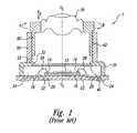
- FIG. 1is a schematic cross-sectional view of a conventional microelectronic imager 1 with a conventional package.
- the imager 1includes a die 10 , an interposer substrate 20 attached to the die 10 , and a housing 30 attached to the interposer substrate 20 .
- the housing 30surrounds the periphery of the die 10 and has an opening 32 .
- the imager 1also includes a transparent cover 40 over the die 10 .
- the die 10includes an image sensor 12 and a plurality of bond-pads 14 electrically coupled to the image sensor 12 .
- the interposer substrate 20is typically a dielectric fixture having a plurality of bond-pads 22 , a plurality of ball-pads 24 , and traces 26 electrically coupling bond-pads 22 to corresponding ball-pads 24 .
- the ball-pads 24are arranged in an array for surface mounting the imager 1 to a board or module of another device.
- the bond-pads 14 on the die 10are electrically coupled to the bond-pads 22 on the interposer substrate 20 by wire-bonds 28 to provide electrical pathways between the bond.-pads 14 and the ball-pads 24 .
- the imager 1 shown in FIG. 1also has an optics unit including a support 50 attached to the housing 30 and a barrel 60 adjustably attached to the support 50 .
- the support 50can include internal threads 52
- the barrel 60can include external threads 62 engaged with the threads 52 .
- the optics unitalso includes a lens 70 carried by the barrel 60 .
- the footprint of the imager 1 in FIG. 1is the surface area of the bottom of the interposer substrate 20 , which is significantly larger than the surface area of the die 10 . Accordingly, the footprint of conventional packaged microelectronic imagers can be a limiting factor in the design and marketability of picture cell phones or PDAs because these devices are continually shrinking to be more portable. Therefore, there is a need to provide microelectronic imagers with smaller footprints and lower vertical profiles.
- Yet another problem of the conventional imager 1 shown in FIG. 1is that moisture and/or other contaminants can impair the performance of the imager 1 .
- the die 10is singulated before the housing 30 and cover 40 are placed over the image sensor 12 .
- the image sensor 12 on the die 10can be damaged by tiny particles generated during the cutting process. Unprotected image sensors can also be damaged by particles or moisture in other process steps. Therefore, there is a need to protect the image sensor during the assembly and packaging of the imager.
- FIG. 1Another concern of conventional microelectronic imagers is the drive to reduce costs for packaging the dies.
- the housing 30 shown in FIG. 1is relatively expensive to form and mount because the cover 40 must be properly aligned and mounted in the opening 32 and the housing 30 must be positioned and mounted to the interposer substrate 20 . This process can be subject to error and is generally time-consuming. Therefore, there is a significant need to enhance the efficiency, reliability, and precision of packaging microelectronic imagers.
- FIG. 1is a schematic cross-sectional view of a packaged microelectronic imager in accordance with the prior art.
- FIGS. 2A and 2Bare schematic side cross-sectional views illustrating subsequent stages in a method for fabricating covers for use in packaging a plurality of microelectronic imaging units at the wafer level in accordance with an embodiment of the invention.
- FIGS. 3A-3Care schematic side cross-sectional views illustrating subsequent stages in a method for packaging a plurality of microelectronic imaging units at the wafer level in accordance with an embodiment of the invention.
- FIGS. 4A and 4Bare schematic side cross-sectional views illustrating various stages in a method for packaging a plurality of microelectronic imaging units at the wafer level in accordance with another embodiment of the invention.
- FIG. 5is a schematic side cross-sectional view illustrating a stage in a method for packaging a plurality of microelectronic imaging units at the wafer level in accordance with another embodiment of the invention.
- FIG. 6is a schematic side cross-sectional view of a packaged microelectronic imager in accordance with one embodiment of the invention.
- FIG. 7is a schematic side cross-sectional view of a packaged microelectronic imager in accordance with another embodiment of the invention.
- the following disclosuredescribes several embodiments of methods for forming and attaching covers to microelectronic imaging units, packaging microelectronic imagers at the wafer level, and microelectronic imagers having covers that protect the image sensor.
- Several embodiments of the inventionattach covers to the imaging units early in the packaging process to protect the image sensors during subsequent assembly and packaging procedures.
- covers for microelectronic imaging units and methods for attaching such covers to microelectronic imaging unitsare expected to significantly reduce the cost for assembling imaging units and produce more robust microelectronic imagers compared to conventional devices.
- the coverscan be formed and installed at the wafer-level, which is expected to significantly enhance the efficiency of manufacturing microelectronic imagers because a plurality of imaging units can be packaged simultaneously using highly accurate and efficient processes developed for fabricating semiconductor devices.
- One aspect of the inventionis directed toward wafer-level processes for forming a plurality of covers for use in microelectronic imaging units.
- An embodiment of one such methodcomprises providing a cover workpiece having a first substrate transmissive to a radiation and a plurality of covers on and/or in the first substrate.
- the covershave windows comprising regions of the first substrate and stand-offs projecting from the windows.
- the methodfurther includes providing a microelectronic workpiece including a second substrate having a plurality of microelectronic dies.
- the dieshave image sensors, integrated circuits electrically coupled to the image sensors, and a plurality of terminals (e.g., bond-pads) electrically coupled to corresponding integrated circuits.
- the methodcontinues by assembling the covers with corresponding dies so that windows are aligned with corresponding image sensors and the stand-offs contact corresponding dies inboard of the terminals and outboard of the image sensors.
- the first substrateis then cut to singulate the individual covers.
- the second substrateis cut to singulate the individual imaging units.
- One-embodiment of a microelectronic imaging unit assembly in accordance with the inventioncomprises a cover workpiece and a microfeature workpiece.
- the cover workpieceincludes a first substrate transmissive to a desired radiation with a plurality of covers.
- the individual coversinclude a window and a stand-off projecting from the window.
- the microfeature workpieceincludes a second substrate with a plurality of microelectronic dies. Individual dies include an image sensor, an integrated circuit electrically coupled to the image sensor, and a plurality of terminals (e.g., bond-pads) electrically coupled to the integrated circuit.
- the first and second substratesare coupled together so that (a) the windows are aligned with corresponding image sensors, and (b) the stand-offs of individual covers are between an individual image sensor and the terminals corresponding to the individual image sensor such that the stand-offs do not completely cover the terminals.
- CMOS imagersto provide a thorough understanding of these embodiments, but other embodiments can be CCD imagers or other types of imagers.
- CCD imagersCCD imagers or other types of imagers.
- Several details describing well-known structures often associated with microelectronic devicesare not set forth in the following description to avoid unnecessarily obscuring the description of the disclosed embodiments.
- the following disclosuresets forth several embodiments of different aspects of the invention, several other embodiments of the invention can have different configurations or different components than those described in this section. As such, it should be understood that the invention may have other embodiments with additional elements or without several of the elements shown and described below with reference to FIGS. 2A-7 .
- FIGS. 2A-3Care schematic side cross-sectional views illustrating stages in a method for fabricating and installing covers used with imaging units in accordance with an embodiment of the invention.
- FIG. 2Ais a schematic side cross-sectional view of a cover workpiece 200 including a first substrate 202 having a first side 204 and a second side 206 opposite the first side 204 .
- the first substrate 202further includes a plurality of discrete device sites 210 at which individual covers are constructed on and/or in the first substrate 202 .
- the device sites 210are arranged in a desired array on the substrate 202 .
- the boundaries of the device sites 210can be defined by cutting lanes A-A along which the first substrate 202 can be cut to singulate individual covers from each other.
- the first substrate 202is transmissive to a desired spectrum of radiation.
- the first substrate 202when the imaging dies are for use in digital cameras, the first substrate 202 is transmissive to light in the visible spectrum.
- the first substrate 202can be transmissive to ultraviolet (UV) light, infrared radiation (IR) and/or any other suitable spectrum according to the particular application of the imaging die.
- the first substrate 202can be composed of glass, quartz, plastics, and/or other suitable materials. In embodiments directed toward imaging radiation in the visible spectrum, the first substrate 202 can also have films that filter UV, IR, or other undesirable spectrums of radiation.
- the first substrate 202for example, can be formed of a material and/or have a coating that filters IR or near IR spectrums, and the first substrate 202 can have an anti-reflective coating.
- FIG. 2Bis a schematic side cross-sectional view of the cover workpiece 200 after forming a plurality of covers 220 on and/or in the first substrate 202 .
- the first substrate 202typically has a cover 220 at each device site 210 .
- the covers 220can be formed together using efficient and highly accurate processes used in semiconductor fabrication technology.
- the covers 220are formed by patterning a layer of resist (not shown) on the first side 204 of the first substrate 202 and etching the first substrate 202 to form stand-offs 222 and a plurality of windows 226 comprising regions of the first substrate 202 between the stand-offs 222 .
- the windows 226 and stand-offs 222 at each device site 210are configured to enclose an image sensor.
- An isotropic etchis used to form the covers 220 on the first substrate 202 , but anisotropic etches and/or other deposition processes may be used to form the covers 220 in other embodiments.
- FIG. 3Ais a schematic side cross-sectional view showing a portion of an imaging unit assembly 300 including a microfeature workpiece 230 and the cover workpiece 200 ( FIG. 2B ) aligned with each other for wafer-level packaging of microelectronic imaging units.
- the microfeature workpiece 230includes a second substrate 232 having a first side 234 , a second side 236 opposite the first side 234 , and a plurality of microelectronic dies 250 formed on and/or in the second substrate 232 .
- the dies 250are arranged in an array on the second substrate 232 , and the covers 220 on the first substrate 202 are arranged in an array corresponding to the arrangement of the dies 250 .
- Individual dies 250can include an integrated circuit 252 (shown schematically), an image sensor 254 operably coupled to the integrated circuit 252 , and a plurality of terminals 256 (e.g., bond-pads) electrically coupled to the integrated circuit 252 .
- the image sensors 254can be CMOS or CCD image sensors for capturing pictures or other images in the visible spectrum. In other embodiments, the image sensors 254 can detect radiation in other spectrums (e.g., IR or UV ranges).
- FIG. 3Bis a schematic side cross-sectional view of the imaging unit assembly 300 after attaching the first substrate 202 to the second substrate 232 .
- the first substrate 202is assembled with the second substrate 232 by placing the stand-offs 222 of the individual covers 220 inboard of the terminals 256 and outboard of the image sensors 254 on corresponding dies 250 .
- Each stand-off 222more specifically, can contact the second substrate 232 in a mounting zone “Z” between an image sensor 254 and the terminals 256 to which the specific image sensor 254 is operatively coupled so that at least a portion of the terminals 256 are exposed.
- the windows 226 of individual covers 220are positioned over corresponding image sensors 254 such that each stand-off 222 and window 226 enclose an image sensor 254 in a recess 224 .
- the windows 226are spaced apart from the image sensors 254 by a gap G to create an enclosed cell 260 .
- the cells 260can be a vacant space sealed under a vacuum to be virtually void of any matter between the image sensors 254 and the windows 226 .
- the cells 260can alternatively be filled with an inert gas having the appropriate tranmissivity to the particular radiation.
- the distal ends of the stand-offs 222can be attached to the second substrate 232 using wafer-level bonding processes known in the semiconductor manufacturing art, such as adhesives (e.g., SU-8 or Benzocyclobutene) or SiO 2 fusion bonding. In other embodiments, different bonding processes may be used.
- wafer-level bonding processesknown in the semiconductor manufacturing art, such as adhesives (e.g., SU-8 or Benzocyclobutene) or SiO 2 fusion bonding. In other embodiments, different bonding processes may be used.
- the first substrate 202is cut along lines A-A to singulate the individual covers 220 and expose the terminals 256 on each die 250 .
- the first substrate 202is cut along lines A-A without contacting the underlying terminals 256 or the second substrate 232 with the cutting blades.
- the first substrate 202is generally cut with blade pairs 270 arranged in a gang, but different methods can be used to cut the first substrate 202 along lines A-A (e.g., a laser).
- the second substrate 232is cut along lines B-B to singulate individual microelectronic imaging units 280 from each other.
- the individual microelectronic imaging units 280can then undergo additional packaging steps, as described below with reference to FIGS. 6 and 7 .
- the image sensors 254are protected within the sealed cells 260 before proceeding with singulating the second substrate 232 or subsequent packaging procedures.
- the covers 220protect the image sensors 254 on the individual dies 250 from fluids and particles while cutting the first or second substrates 202 or 232 . A single small particle can ruin an image sensor 254 for high-end applications, such as digital cameras and picture cell phones.
- the covers 220by attaching the covers 220 at the wafer level before singulating the individual dies 250 , the image sensors 254 on the individual dies 250 are protected during the singulation process. Further, the image sensors 254 on the individual dies 250 are also protected during subsequent packaging and assembly processes, such as wire-bonding and/or encapsulation.
- the stand-offs 222are integral components of the individual covers 220 -and are attached to the individual dies 250 to accurately position each cover 220 over corresponding image sensors 254 on the dies 250 .
- This is an efficient manufacturing processbecause there is no need for additional steps or processes to construct spacer elements on the dies 250 , mount individual cover windows to such spacers, or mount a separate housing to an interposer substrate.
- the stand-offs 222 on the covers 220provide very precise control of the stand-off distance for the covers 220 with respect to the image sensors 254 .
- FIGS. 4A and 4Billustrate stages in a method for fabricating microelectronic imaging units in accordance with another embodiment of the invention.
- the first substrate 202is initially processed as shown and described above with reference to FIGS. 2 A-B.
- FIG. 4Ais a schematic side cross-sectional view of the cover workpiece 200 illustrated in FIG. 2B in hypothetical alignment with the microfeature workpiece 230 shown in FIG. 3A .
- the first substrate 202is cut to singulate the individual covers 220 before attaching the covers 220 to the microfeature workpiece 230 .
- the first substrate 202is accordingly cut along lines C-C to separate individual covers 220 from each other before aligning the covers 220 with the image sensors 254 .
- the individual covers 220are aligned with corresponding image sensors 254 and attached to the second substrate 232 .
- the windows 226are individually installed at a desired location relative to one of the image sensors 254 on the individual dies 250 .
- the second substrate 232is cut along lines D-D to construct a plurality of microelectronic imaging units as illustrated in FIG. 3C .
- One advantage of this embodimentis that the dies 250 can be tested to determine known-good dies 250 before attaching the covers 220 to the individual dies 250 . As such, the covers 220 can be attached to only the known-good dies 250 to avoid wasting good covers.
- FIG. 5is a schematic side cross-sectional view showing a cover workpiece 500 in accordance with another embodiment of the invention.
- the cover workpiece 500includes a first substrate 502 having a first side 504 and a second side 506 opposite the first side 504 .
- the cover workpiece 500further includes a plurality of discrete device sites 510 at which individual covers are constructed on the first substrate 502 .
- the boundaries of the device sites 510can be defined by cutting lanes E-E along which the first substrate 502 can be cut to singulate individual covers from each other.
- the first substrate 502can be at least generally similar to the first substrate 202 described above with reference to FIG. 2A .
- the first substrate 502further includes a plurality of stand-offs 522 on one side (e.g., the first side 504 ) of the first substrate 502 .
- the stand-offs 522can be composed of the same material as the first substrate 502 , but the stand-offs 522 are generally composed of a different material.
- the first substrate 502can be quartz and the stand-offs 522 can be an epoxy or other polymer.
- the stand-offs 522project away from the first substrate 502 at the individual device sites 510 in a pattern corresponding to the pattern of image sensors 254 and terminals 256 on the microfeature workpiece 230 ( FIG. 3A ).
- the stand-offs 522create a recess 524 at each device site 510 , and the regions of the first substrate 502 between the stand-offs 522 are windows 526 .
- the stand-offs 522can be formed on the first substrate 502 using screen-printing processes, three-dimensional stereolithography techniques, or other disposing processes. In still further embodiments, the stand-offs 522 are formed on the first substrate 502 by molding material onto the substrate or attaching pre-formed stand-offs onto the substrate. After the plurality of stand-offs 522 have been formed on the first substrate 502 , the cover workpiece 500 can be cut along lines E-E either before or after attaching the stand-offs 522 to the second substrate 232 as shown in either FIG. 3B or FIG. 4B .
- FIGS. 2A-5 and the associated text abovedescribe several embodiments of fabricating covers and imaging units for use in microelectronic imagers.
- the covers and/or the imaging unitscan be formed using other methods and they can have other configurations. Accordingly, the present invention is not limited to the particular methods and/or structures described above, but it also includes alternative methods for fabricating the covers and imaging units.
- FIGS. 6 and 7illustrate different embodiments of methods for packaging microelectronic imagers using imaging units with covers as described above. Although the following embodiments illustrate packaging only a single microelectronic imager, it will be appreciated that a plurality of imagers can be packaged simultaneously at the wafer level.
- FIG. 6is a schematic side cross-sectional view of a packaged microelectronic imager 600 in accordance with an embodiment of the invention.
- the imager 600 in the illustrated embodimentincludes an imaging unit 680 including the cover 220 described above with respect to FIG. 3C and a microelectronic die 650 .
- the die 650has a front side 610 and a backside 611 .
- the die 650further includes an integrated circuit 652 (shown schematically), an image sensor 654 operably coupled to the integrated circuit 652 , and an array of terminals 656 (e.g., bond-pads) electrically coupled to the integrated circuit 652 .
- an integrated circuit 652shown schematically
- an image sensor 654operably coupled to the integrated circuit 652
- an array of terminals 656e.g., bond-pads
- the die 650differs from the die 250 shown in FIG. 3C in that the die 650 has a plurality of electrically conductive interconnects 657 having a first portion electrically coupled to corresponding terminals 656 and a second portion electrically coupled to corresponding ball-pads 658 on the second side 611 of the die 650 .
- the interconnects 657are thus through-wafer interconnects that extend completely through the die 650 from the first side 610 to the second side 611 .
- other diesmay not include through-wafer type interconnects 657 .
- the interconnects 657can be formed according to the processes disclosed in U.S. patent application Ser. No.
- the interconnects 657can be formed in the die 650 either before or after singulating the dies 650 ( FIG. 3C ).
- the ball-pads 658are formed on and/or in the second side 611 of the die 650 and are configured to receive solder balls (not shown) or other conductive elements. In other embodiments, the imager 600 may not include the ball-pads 658 and/or the solder balls.
- the imager 600can further include an optics unit 690 attached to the cover 220 and aligned with the image sensor 654 .
- the optics unit 690can include a plate 692 and an optic member 694 on the plate 692 to transmit at least the desired spectrum of radiation to the image sensor 654 .
- the optic member 694can be a lens for focusing the light, pinholes for reducing higher order refractions, and/or other optical structures for performing other functions.
- the plate 692 and optic member 694are supported by a support member 696 that accurately situates the optic member 694 at a desired location with respect to the image sensor 654 .
- Suitable support members 696 with corresponding interface featuresare disclosed in U.S. application Ser. No. 10/723,363, entitled “Packaged Microelectronic Imagers and Methods of Packaging Microelectronic Imagers,” filed on Nov. 26, 2003 (Perkins Coie Docket No. 108298746US), which is herein incorporated by reference in its entirety.
- the plate 692is attached to the support member 696 in the embodiment shown in FIG. 6 , but other embodiments of the optics unit 690 may not include a plate such that the optic member 694 is attached directly to the support member 696 .
- the imager 600 illustrated in FIG. 6can be much smaller than the conventional imager shown in FIG. 1 .
- the footprint of the imager 600can be as small as the size of the die 650 because the die is not mounted to a separate interposer substrate. This is possible because the interconnects 657 provide an electrical connection to the array of ball-pads 658 on the second side 611 of the die 650 instead of using wire-bonds on the first side 610 of the die 650 .
- the height of the imager 600is also less than with conventional imagers because the imager 600 can be mounted directly to a module or board without an interposer substrate. Therefore, the imager 600 is expected to have a smaller footprint and a lower profile than conventional microelectronic imagers, which is particularly advantageous for picture cell phones, PDAs, or other applications where space is limited.
- a further advantage of the imager 600 illustrated in FIG. 6is that the imager 600 can be tested from the backside 611 of the die 650 .
- a test probecan contact the backside 611 of the die 650 to test the imager 600 because the through-wafer interconnects 657 provide backside electrical contacts (e.g., ball-pads 658 ). Accordingly, because the test probe engages contacts on the backside 611 of the die 650 , it will not damage the image sensor 654 , the optics units 690 , or associated circuitry on the front of the die 650 .
- test probedoes not obstruct the image sensor 654 during a backside test, which allows the test probe to more easily test the imager compared to processes that test imaging dies from the front side. Furthermore, it is advantageous to test the microelectronic imager 600 in an environment where the image sensor 654 and/or optics unit 690 will not be damaged during testing.
- FIG. 7is a schematic side cross-sectional view of a packaged microelectronic imager 700 in accordance with another embodiment of the invention.
- the imager 700 in the illustrated embodimentcan include the imaging unit 280 described above with respect to FIG. 3C , the optics unit 690 described above in FIG. 6 , and an interposer substrate 702 ; like reference numbers accordingly refer to like components in FIGS. 3C, 6 , and 7 .
- the interposer substrate 702includes a first side 704 having a plurality of contacts 766 and a second side 706 having a plurality of pads 768 .
- the interposer substrate 702further includes a plurality of traces 767 electrically coupling individual contacts 766 to corresponding pads 768 .
- the contacts 766can be arranged in arrays for attachment to the corresponding terminals 256 on the die 250
- the pads 768can be arranged in arrays for attachment to a plurality of electrical couplers (e.g., solder balls).
- the imaging unit 280can be attached to the interposer substrate 702 with an adhesive film, an epoxy, or another suitable material. After attaching the imaging unit 280 to the interposer substrate 702 , a plurality of wire-bonds 722 are formed to electrically couple the die 250 to the interposer substrate 702 .
- the imager 700can further include the optics unit 690 attached to the cover 220 and aligned with the image sensor 254 .
- microelectronic imaging units and microelectronic imagerscan have any combination of the features described above with reference to FIGS. 2A-7 . Accordingly, the invention is not limited except as by the appended claims.
Landscapes
- Engineering & Computer Science (AREA)
- Multimedia (AREA)
- Signal Processing (AREA)
- Solid State Image Pick-Up Elements (AREA)
- Transforming Light Signals Into Electric Signals (AREA)
Abstract
Description
- The present invention is related to microelectronic devices and methods for packaging microelectronic devices. Several aspects of the present invention are directed toward covers for protecting image sensors and methods for wafer-level packaging of microelectronic imaging units that are responsive to radiation in the visible light spectrum or in other spectrums.
- Microelectronic imagers are used in digital cameras, wireless devices with picture capabilities, and many other applications. Cell phones and Personal Digital Assistants (PDAs), for example, incorporate microelectronic imagers for capturing and sending pictures. The growth rate of microelectronic imagers has been steadily increasing as they become smaller and produce better images with higher pixel counts.
- Microelectronic imagers include image sensors that use Charged Coupled Device (CCD) systems, Complementary Metal-Oxide Semiconductor (CMOS) systems, or other systems. CCD image sensors have been widely used in digital cameras and other applications. CMOS image sensors are also becoming very popular because they have low production costs, high yields, and small sizes. CMOS image sensors provide these advantages because they are manufactured using technology and equipment developed for fabricating semiconductor devices. CMOS image sensors, as well as CCD image sensors, are accordingly “packaged” to protect their delicate components and provide external electrical contacts.
FIG. 1 is a schematic cross-sectional view of a conventionalmicroelectronic imager 1 with a conventional package. Theimager 1 includes adie 10, aninterposer substrate 20 attached to thedie 10, and ahousing 30 attached to theinterposer substrate 20. Thehousing 30 surrounds the periphery of the die10 and has anopening 32. Theimager 1 also includes atransparent cover 40 over the die10.- The die10 includes an
image sensor 12 and a plurality of bond-pads 14 electrically coupled to theimage sensor 12. Theinterposer substrate 20 is typically a dielectric fixture having a plurality of bond-pads 22, a plurality of ball-pads 24, and traces26 electrically coupling bond-pads 22 to corresponding ball-pads 24. The ball-pads 24 are arranged in an array for surface mounting theimager 1 to a board or module of another device. The bond-pads 14 on thedie 10 are electrically coupled to the bond-pads 22 on theinterposer substrate 20 by wire-bonds 28 to provide electrical pathways between the bond.-pads 14 and the ball-pads 24. - The
imager 1 shown inFIG. 1 also has an optics unit including asupport 50 attached to thehousing 30 and abarrel 60 adjustably attached to thesupport 50. Thesupport 50 can includeinternal threads 52, and thebarrel 60 can includeexternal threads 62 engaged with thethreads 52. The optics unit also includes alens 70 carried by thebarrel 60. - One problem with conventional packaged microelectronic imagers is that they have relatively large footprints and occupy a significant amount of vertical space (i.e., high profiles). For example, the footprint of the
imager 1 inFIG. 1 is the surface area of the bottom of theinterposer substrate 20, which is significantly larger than the surface area of thedie 10. Accordingly, the footprint of conventional packaged microelectronic imagers can be a limiting factor in the design and marketability of picture cell phones or PDAs because these devices are continually shrinking to be more portable. Therefore, there is a need to provide microelectronic imagers with smaller footprints and lower vertical profiles. - Yet another problem of the
conventional imager 1 shown inFIG. 1 is that moisture and/or other contaminants can impair the performance of theimager 1. For example, thedie 10 is singulated before thehousing 30 andcover 40 are placed over theimage sensor 12. Accordingly, theimage sensor 12 on thedie 10 can be damaged by tiny particles generated during the cutting process. Unprotected image sensors can also be damaged by particles or moisture in other process steps. Therefore, there is a need to protect the image sensor during the assembly and packaging of the imager. - Another concern of conventional microelectronic imagers is the drive to reduce costs for packaging the dies. The
housing 30 shown inFIG. 1 is relatively expensive to form and mount because thecover 40 must be properly aligned and mounted in theopening 32 and thehousing 30 must be positioned and mounted to theinterposer substrate 20. This process can be subject to error and is generally time-consuming. Therefore, there is a significant need to enhance the efficiency, reliability, and precision of packaging microelectronic imagers. FIG. 1 is a schematic cross-sectional view of a packaged microelectronic imager in accordance with the prior art.FIGS. 2A and 2B are schematic side cross-sectional views illustrating subsequent stages in a method for fabricating covers for use in packaging a plurality of microelectronic imaging units at the wafer level in accordance with an embodiment of the invention.FIGS. 3A-3C are schematic side cross-sectional views illustrating subsequent stages in a method for packaging a plurality of microelectronic imaging units at the wafer level in accordance with an embodiment of the invention.FIGS. 4A and 4B are schematic side cross-sectional views illustrating various stages in a method for packaging a plurality of microelectronic imaging units at the wafer level in accordance with another embodiment of the invention.FIG. 5 is a schematic side cross-sectional view illustrating a stage in a method for packaging a plurality of microelectronic imaging units at the wafer level in accordance with another embodiment of the invention.FIG. 6 is a schematic side cross-sectional view of a packaged microelectronic imager in accordance with one embodiment of the invention.FIG. 7 is a schematic side cross-sectional view of a packaged microelectronic imager in accordance with another embodiment of the invention.- A. Overview
- The following disclosure describes several embodiments of methods for forming and attaching covers to microelectronic imaging units, packaging microelectronic imagers at the wafer level, and microelectronic imagers having covers that protect the image sensor. Several embodiments of the invention attach covers to the imaging units early in the packaging process to protect the image sensors during subsequent assembly and packaging procedures. Several embodiments of covers for microelectronic imaging units and methods for attaching such covers to microelectronic imaging units are expected to significantly reduce the cost for assembling imaging units and produce more robust microelectronic imagers compared to conventional devices. Moreover, the covers can be formed and installed at the wafer-level, which is expected to significantly enhance the efficiency of manufacturing microelectronic imagers because a plurality of imaging units can be packaged simultaneously using highly accurate and efficient processes developed for fabricating semiconductor devices.
- One aspect of the invention is directed toward wafer-level processes for forming a plurality of covers for use in microelectronic imaging units. An embodiment of one such method comprises providing a cover workpiece having a first substrate transmissive to a radiation and a plurality of covers on and/or in the first substrate. The covers have windows comprising regions of the first substrate and stand-offs projecting from the windows. The method further includes providing a microelectronic workpiece including a second substrate having a plurality of microelectronic dies. The dies have image sensors, integrated circuits electrically coupled to the image sensors, and a plurality of terminals (e.g., bond-pads) electrically coupled to corresponding integrated circuits. The method continues by assembling the covers with corresponding dies so that windows are aligned with corresponding image sensors and the stand-offs contact corresponding dies inboard of the terminals and outboard of the image sensors. The first substrate is then cut to singulate the individual covers. After cutting the first substrate, the second substrate is cut to singulate the individual imaging units.
- Another aspect of the present invention is directed toward microelectronic imaging unit assemblies that are packaged or otherwise used in wafer-level packaging of microelectronic imaging units. One-embodiment of a microelectronic imaging unit assembly in accordance with the invention comprises a cover workpiece and a microfeature workpiece. The cover workpiece includes a first substrate transmissive to a desired radiation with a plurality of covers. The individual covers include a window and a stand-off projecting from the window. The microfeature workpiece includes a second substrate with a plurality of microelectronic dies. Individual dies include an image sensor, an integrated circuit electrically coupled to the image sensor, and a plurality of terminals (e.g., bond-pads) electrically coupled to the integrated circuit. The first and second substrates are coupled together so that (a) the windows are aligned with corresponding image sensors, and (b) the stand-offs of individual covers are between an individual image sensor and the terminals corresponding to the individual image sensor such that the stand-offs do not completely cover the terminals.
- Specific details of several embodiments of the invention are described below with reference to CMOS imagers to provide a thorough understanding of these embodiments, but other embodiments can be CCD imagers or other types of imagers. Several details describing well-known structures often associated with microelectronic devices are not set forth in the following description to avoid unnecessarily obscuring the description of the disclosed embodiments. Moreover, although the following disclosure sets forth several embodiments of different aspects of the invention, several other embodiments of the invention can have different configurations or different components than those described in this section. As such, it should be understood that the invention may have other embodiments with additional elements or without several of the elements shown and described below with reference to
FIGS. 2A-7 . - B. Fabricating Imaging Units for Use in Microelectronic Imagers
FIGS. 2A-3C are schematic side cross-sectional views illustrating stages in a method for fabricating and installing covers used with imaging units in accordance with an embodiment of the invention.FIG. 2A , more specifically, is a schematic side cross-sectional view of acover workpiece 200 including afirst substrate 202 having afirst side 204 and asecond side 206 opposite thefirst side 204. Thefirst substrate 202 further includes a plurality ofdiscrete device sites 210 at which individual covers are constructed on and/or in thefirst substrate 202. Thedevice sites 210 are arranged in a desired array on thesubstrate 202. The boundaries of thedevice sites 210 can be defined by cutting lanes A-A along which thefirst substrate 202 can be cut to singulate individual covers from each other.- The
first substrate 202 is transmissive to a desired spectrum of radiation. For example, when the imaging dies are for use in digital cameras, thefirst substrate 202 is transmissive to light in the visible spectrum. Thefirst substrate 202, however, can be transmissive to ultraviolet (UV) light, infrared radiation (IR) and/or any other suitable spectrum according to the particular application of the imaging die. Thefirst substrate 202 can be composed of glass, quartz, plastics, and/or other suitable materials. In embodiments directed toward imaging radiation in the visible spectrum, thefirst substrate 202 can also have films that filter UV, IR, or other undesirable spectrums of radiation. Thefirst substrate 202, for example, can be formed of a material and/or have a coating that filters IR or near IR spectrums, and thefirst substrate 202 can have an anti-reflective coating. FIG. 2B is a schematic side cross-sectional view of thecover workpiece 200 after forming a plurality ofcovers 220 on and/or in thefirst substrate 202. Thefirst substrate 202 typically has acover 220 at eachdevice site 210. Thecovers 220 can be formed together using efficient and highly accurate processes used in semiconductor fabrication technology. In one embodiment, thecovers 220 are formed by patterning a layer of resist (not shown) on thefirst side 204 of thefirst substrate 202 and etching thefirst substrate 202 to form stand-offs 222 and a plurality ofwindows 226 comprising regions of thefirst substrate 202 between the stand-offs 222. Thewindows 226 and stand-offs 222 at eachdevice site 210 are configured to enclose an image sensor. An isotropic etch is used to form thecovers 220 on thefirst substrate 202, but anisotropic etches and/or other deposition processes may be used to form thecovers 220 in other embodiments.FIG. 3A is a schematic side cross-sectional view showing a portion of animaging unit assembly 300 including amicrofeature workpiece 230 and the cover workpiece200 (FIG. 2B ) aligned with each other for wafer-level packaging of microelectronic imaging units. Themicrofeature workpiece 230 includes asecond substrate 232 having afirst side 234, asecond side 236 opposite thefirst side 234, and a plurality of microelectronic dies250 formed on and/or in thesecond substrate 232. The dies250 are arranged in an array on thesecond substrate 232, and thecovers 220 on thefirst substrate 202 are arranged in an array corresponding to the arrangement of the dies250. Individual dies250 can include an integrated circuit252 (shown schematically), animage sensor 254 operably coupled to theintegrated circuit 252, and a plurality of terminals256 (e.g., bond-pads) electrically coupled to theintegrated circuit 252. Theimage sensors 254 can be CMOS or CCD image sensors for capturing pictures or other images in the visible spectrum. In other embodiments, theimage sensors 254 can detect radiation in other spectrums (e.g., IR or UV ranges).FIG. 3B is a schematic side cross-sectional view of theimaging unit assembly 300 after attaching thefirst substrate 202 to thesecond substrate 232. Thefirst substrate 202 is assembled with thesecond substrate 232 by placing the stand-offs 222 of the individual covers220 inboard of theterminals 256 and outboard of theimage sensors 254 on corresponding dies250. Each stand-off 222, more specifically, can contact thesecond substrate 232 in a mounting zone “Z” between animage sensor 254 and theterminals 256 to which thespecific image sensor 254 is operatively coupled so that at least a portion of theterminals 256 are exposed. Thewindows 226 ofindividual covers 220 are positioned overcorresponding image sensors 254 such that each stand-off222 andwindow 226 enclose animage sensor 254 in arecess 224. Thewindows 226 are spaced apart from theimage sensors 254 by a gap G to create anenclosed cell 260. Thecells 260 can be a vacant space sealed under a vacuum to be virtually void of any matter between theimage sensors 254 and thewindows 226. Thecells 260 can alternatively be filled with an inert gas having the appropriate tranmissivity to the particular radiation. The distal ends of the stand-offs 222 can be attached to thesecond substrate 232 using wafer-level bonding processes known in the semiconductor manufacturing art, such as adhesives (e.g., SU-8 or Benzocyclobutene) or SiO2fusion bonding. In other embodiments, different bonding processes may be used.- After attaching the
first substrate 202 to thesecond substrate 232 as described above, thefirst substrate 202 is cut along lines A-A to singulate the individual covers220 and expose theterminals 256 on each die250. Thefirst substrate 202 is cut along lines A-A without contacting theunderlying terminals 256 or thesecond substrate 232 with the cutting blades. Thefirst substrate 202 is generally cut with blade pairs270 arranged in a gang, but different methods can be used to cut thefirst substrate 202 along lines A-A (e.g., a laser). - Referring next to
FIG. 3C , thesecond substrate 232 is cut along lines B-B to singulate individualmicroelectronic imaging units 280 from each other. The individualmicroelectronic imaging units 280 can then undergo additional packaging steps, as described below with reference toFIGS. 6 and 7 . - One advantage of several embodiments for fabricating microelectronic imaging units described above with respect to
FIGS. 2A-3C is that theimage sensors 254 are protected within the sealedcells 260 before proceeding with singulating thesecond substrate 232 or subsequent packaging procedures. For example, thecovers 220 protect theimage sensors 254 on the individual dies250 from fluids and particles while cutting the first orsecond substrates image sensor 254 for high-end applications, such as digital cameras and picture cell phones. However, by attaching thecovers 220 at the wafer level before singulating the individual dies250, theimage sensors 254 on the individual dies250 are protected during the singulation process. Further, theimage sensors 254 on the individual dies250 are also protected during subsequent packaging and assembly processes, such as wire-bonding and/or encapsulation. - Yet another advantage of the processes for fabricating the
imaging units 280 described above is that there is no need for additional spacers or support members to support thecovers 220 over the individual dies250. The stand-offs 222 are integral components of the individual covers220-and are attached to the individual dies250 to accurately position eachcover 220 overcorresponding image sensors 254 on the dies250. This is an efficient manufacturing process because there is no need for additional steps or processes to construct spacer elements on the dies250, mount individual cover windows to such spacers, or mount a separate housing to an interposer substrate. Further, the stand-offs 222 on thecovers 220 provide very precise control of the stand-off distance for thecovers 220 with respect to theimage sensors 254. FIGS. 4A and 4B illustrate stages in a method for fabricating microelectronic imaging units in accordance with another embodiment of the invention. Thefirst substrate 202 is initially processed as shown and described above with reference to FIGS.2A-B.FIG. 4A is a schematic side cross-sectional view of thecover workpiece 200 illustrated inFIG. 2B in hypothetical alignment with themicrofeature workpiece 230 shown inFIG. 3A . Unlike the process described inFIGS. 3A-3C , however, thefirst substrate 202 is cut to singulate the individual covers220 before attaching thecovers 220 to themicrofeature workpiece 230. Thefirst substrate 202 is accordingly cut along lines C-C to separateindividual covers 220 from each other before aligning thecovers 220 with theimage sensors 254.- Referring next to
FIG. 4B , the individual covers220 are aligned withcorresponding image sensors 254 and attached to thesecond substrate 232. Thewindows 226 are individually installed at a desired location relative to one of theimage sensors 254 on the individual dies250. After the individual covers220 have been attached to the corresponding dies250, thesecond substrate 232 is cut along lines D-D to construct a plurality of microelectronic imaging units as illustrated inFIG. 3C . One advantage of this embodiment is that the dies250 can be tested to determine known-good dies250 before attaching thecovers 220 to the individual dies250. As such, thecovers 220 can be attached to only the known-good dies250 to avoid wasting good covers. FIG. 5 is a schematic side cross-sectional view showing acover workpiece 500 in accordance with another embodiment of the invention. Thecover workpiece 500 includes afirst substrate 502 having afirst side 504 and asecond side 506 opposite thefirst side 504. Thecover workpiece 500 further includes a plurality ofdiscrete device sites 510 at which individual covers are constructed on thefirst substrate 502. The boundaries of thedevice sites 510 can be defined by cutting lanes E-E along which thefirst substrate 502 can be cut to singulate individual covers from each other. Thefirst substrate 502 can be at least generally similar to thefirst substrate 202 described above with reference toFIG. 2A .- The
first substrate 502 further includes a plurality of stand-offs 522 on one side (e.g., the first side504) of thefirst substrate 502. The stand-offs 522 can be composed of the same material as thefirst substrate 502, but the stand-offs 522 are generally composed of a different material. For example, thefirst substrate 502 can be quartz and the stand-offs 522 can be an epoxy or other polymer. The stand-offs 522 project away from thefirst substrate 502 at theindividual device sites 510 in a pattern corresponding to the pattern ofimage sensors 254 andterminals 256 on the microfeature workpiece230 (FIG. 3A ). The stand-offs 522 create arecess 524 at eachdevice site 510, and the regions of thefirst substrate 502 between the stand-offs 522 arewindows 526. - The stand-
offs 522 can be formed on thefirst substrate 502 using screen-printing processes, three-dimensional stereolithography techniques, or other disposing processes. In still further embodiments, the stand-offs 522 are formed on thefirst substrate 502 by molding material onto the substrate or attaching pre-formed stand-offs onto the substrate. After the plurality of stand-offs 522 have been formed on thefirst substrate 502, thecover workpiece 500 can be cut along lines E-E either before or after attaching the stand-offs 522 to thesecond substrate 232 as shown in eitherFIG. 3B orFIG. 4B . FIGS. 2A-5 and the associated text above describe several embodiments of fabricating covers and imaging units for use in microelectronic imagers. The covers and/or the imaging units, however, can be formed using other methods and they can have other configurations. Accordingly, the present invention is not limited to the particular methods and/or structures described above, but it also includes alternative methods for fabricating the covers and imaging units.- C. Packaging of Microelectronic Imagers
FIGS. 6 and 7 illustrate different embodiments of methods for packaging microelectronic imagers using imaging units with covers as described above. Although the following embodiments illustrate packaging only a single microelectronic imager, it will be appreciated that a plurality of imagers can be packaged simultaneously at the wafer level.FIG. 6 is a schematic side cross-sectional view of a packagedmicroelectronic imager 600 in accordance with an embodiment of the invention. Theimager 600 in the illustrated embodiment includes animaging unit 680 including thecover 220 described above with respect toFIG. 3C and amicroelectronic die 650. Like reference numbers refer to like components inFIGS. 3C and 6 . Thedie 650 has afront side 610 and abackside 611. The die650 further includes an integrated circuit652 (shown schematically), animage sensor 654 operably coupled to theintegrated circuit 652, and an array of terminals656 (e.g., bond-pads) electrically coupled to theintegrated circuit 652.- The
die 650 differs from thedie 250 shown inFIG. 3C in that thedie 650 has a plurality of electricallyconductive interconnects 657 having a first portion electrically coupled tocorresponding terminals 656 and a second portion electrically coupled to corresponding ball-pads 658 on thesecond side 611 of thedie 650. In the embodiment shown inFIG. 6 , theinterconnects 657 are thus through-wafer interconnects that extend completely through the die650 from thefirst side 610 to thesecond side 611. Alternatively, other dies may not include through-wafer type interconnects657. Theinterconnects 657 can be formed according to the processes disclosed in U.S. patent application Ser. No. 10/713,878, entitled “Microelectronic Devices, Methods for Forming Vias in Microelectronic Devices, and Methods for Packaging Microelectronic Devices,” filed on Nov. 13, 2003 (Perkins Coie Docket No. 108298742US), which is herein incorporated by reference in its entirety. Theinterconnects 657 can be formed in thedie 650 either before or after singulating the dies650 (FIG. 3C ). The ball-pads 658 are formed on and/or in thesecond side 611 of thedie 650 and are configured to receive solder balls (not shown) or other conductive elements. In other embodiments, theimager 600 may not include the ball-pads 658 and/or the solder balls. - In another aspect of the embodiment illustrated in
FIG. 6 , theimager 600 can further include anoptics unit 690 attached to thecover 220 and aligned with theimage sensor 654. Theoptics unit 690 can include aplate 692 and anoptic member 694 on theplate 692 to transmit at least the desired spectrum of radiation to theimage sensor 654. Theoptic member 694 can be a lens for focusing the light, pinholes for reducing higher order refractions, and/or other optical structures for performing other functions. - The
plate 692 andoptic member 694 are supported by asupport member 696 that accurately situates theoptic member 694 at a desired location with respect to theimage sensor 654.Suitable support members 696 with corresponding interface features are disclosed in U.S. application Ser. No. 10/723,363, entitled “Packaged Microelectronic Imagers and Methods of Packaging Microelectronic Imagers,” filed on Nov. 26, 2003 (Perkins Coie Docket No. 108298746US), which is herein incorporated by reference in its entirety. Theplate 692 is attached to thesupport member 696 in the embodiment shown inFIG. 6 , but other embodiments of theoptics unit 690 may not include a plate such that theoptic member 694 is attached directly to thesupport member 696. - One advantage of the
imager 600 illustrated inFIG. 6 is that theimager 600 can be much smaller than the conventional imager shown inFIG. 1 . The footprint of theimager 600 can be as small as the size of thedie 650 because the die is not mounted to a separate interposer substrate. This is possible because theinterconnects 657 provide an electrical connection to the array of ball-pads 658 on thesecond side 611 of thedie 650 instead of using wire-bonds on thefirst side 610 of thedie 650. The height of theimager 600 is also less than with conventional imagers because theimager 600 can be mounted directly to a module or board without an interposer substrate. Therefore, theimager 600 is expected to have a smaller footprint and a lower profile than conventional microelectronic imagers, which is particularly advantageous for picture cell phones, PDAs, or other applications where space is limited. - A further advantage of the
imager 600 illustrated inFIG. 6 is that theimager 600 can be tested from thebackside 611 of thedie 650. A test probe can contact thebackside 611 of the die650 to test theimager 600 because the through-wafer interconnects 657 provide backside electrical contacts (e.g., ball-pads658). Accordingly, because the test probe engages contacts on thebackside 611 of thedie 650, it will not damage theimage sensor 654, theoptics units 690, or associated circuitry on the front of thedie 650. Moreover, the test probe does not obstruct theimage sensor 654 during a backside test, which allows the test probe to more easily test the imager compared to processes that test imaging dies from the front side. Furthermore, it is advantageous to test themicroelectronic imager 600 in an environment where theimage sensor 654 and/oroptics unit 690 will not be damaged during testing. FIG. 7 is a schematic side cross-sectional view of a packagedmicroelectronic imager 700 in accordance with another embodiment of the invention. Theimager 700 in the illustrated embodiment can include theimaging unit 280 described above with respect toFIG. 3C , theoptics unit 690 described above inFIG. 6 , and aninterposer substrate 702; like reference numbers accordingly refer to like components inFIGS. 3C, 6 , and7. Theinterposer substrate 702 includes afirst side 704 having a plurality ofcontacts 766 and asecond side 706 having a plurality ofpads 768. Theinterposer substrate 702 further includes a plurality oftraces 767 electrically couplingindividual contacts 766 tocorresponding pads 768. Thecontacts 766 can be arranged in arrays for attachment to thecorresponding terminals 256 on thedie 250, and thepads 768 can be arranged in arrays for attachment to a plurality of electrical couplers (e.g., solder balls).- The
imaging unit 280 can be attached to theinterposer substrate 702 with an adhesive film, an epoxy, or another suitable material. After attaching theimaging unit 280 to theinterposer substrate 702, a plurality of wire-bonds 722 are formed to electrically couple the die250 to theinterposer substrate 702. Theimager 700 can further include theoptics unit 690 attached to thecover 220 and aligned with theimage sensor 254. - From the foregoing, it will be appreciated that specific embodiments of the invention have been described herein for purposes of illustration, but that various modifications may be made without deviating from the spirit and scope of the invention. For example, the microelectronic imaging units and microelectronic imagers can have any combination of the features described above with reference to
FIGS. 2A-7 . Accordingly, the invention is not limited except as by the appended claims.
Claims (80)
Priority Applications (7)
| Application Number | Priority Date | Filing Date | Title |
|---|---|---|---|
| US10/845,304US8092734B2 (en) | 2004-05-13 | 2004-05-13 | Covers for microelectronic imagers and methods for wafer-level packaging of microelectronics imagers |
| KR1020067026151AKR100846962B1 (en) | 2004-05-13 | 2005-04-27 | Wafer-Level Packaging of Microelectronic Imagers and Covers for Microelectronic Imagers |
| PCT/US2005/014632WO2005114750A1 (en) | 2004-05-13 | 2005-04-27 | Covers for microelectronic imagers and methods for wafer-level packaging of microelectronic imagers |
| JP2007513178AJP2007537670A (en) | 2004-05-13 | 2005-04-27 | Cover for microelectronic imager and method for packaging microelectronic imager at wafer level |
| CN2005800238502ACN1985379B (en) | 2004-05-13 | 2005-04-27 | Covers for microelectronic imagers and methods for wafer-level packaging of microelectronic imagers |
| EP05741899.8AEP1747591B1 (en) | 2004-05-13 | 2005-04-27 | Covers for microelectronic imagers and method for wafer-level packaging of microelectronic imagers |
| TW094115463ATWI264118B (en) | 2004-05-13 | 2005-05-12 | Covers for microelectronic imagers and methods for wafer-level packaging of microelectronic imagers |
Applications Claiming Priority (1)
| Application Number | Priority Date | Filing Date | Title |
|---|---|---|---|
| US10/845,304US8092734B2 (en) | 2004-05-13 | 2004-05-13 | Covers for microelectronic imagers and methods for wafer-level packaging of microelectronics imagers |
Publications (2)
| Publication Number | Publication Date |
|---|---|
| US20050253213A1true US20050253213A1 (en) | 2005-11-17 |
| US8092734B2 US8092734B2 (en) | 2012-01-10 |
Family
ID=34967912
Family Applications (1)
| Application Number | Title | Priority Date | Filing Date |
|---|---|---|---|
| US10/845,304Active2028-01-01US8092734B2 (en) | 2004-05-13 | 2004-05-13 | Covers for microelectronic imagers and methods for wafer-level packaging of microelectronics imagers |
Country Status (7)
| Country | Link |
|---|---|
| US (1) | US8092734B2 (en) |
| EP (1) | EP1747591B1 (en) |
| JP (1) | JP2007537670A (en) |
| KR (1) | KR100846962B1 (en) |
| CN (1) | CN1985379B (en) |
| TW (1) | TWI264118B (en) |
| WO (1) | WO2005114750A1 (en) |
Cited By (81)
| Publication number | Priority date | Publication date | Assignee | Title |
|---|---|---|---|---|
| US20050275750A1 (en)* | 2004-06-09 | 2005-12-15 | Salman Akram | Wafer-level packaged microelectronic imagers and processes for wafer-level packaging |
| US20060040421A1 (en)* | 2004-08-19 | 2006-02-23 | Farnworth Warren M | Spacers for packaged microelectronic imagers and methods of making and using spacers for wafer-level packaging of imagers |
| US20060043555A1 (en)* | 2004-08-24 | 2006-03-02 | Liu Chung Y | Sensor package |
| US20060216850A1 (en)* | 2004-08-10 | 2006-09-28 | Street Bret K | Microelectronic imaging units and methods of manufacturing microelectronic imaging units |
| WO2007006378A1 (en)* | 2005-07-08 | 2007-01-18 | Tridonic Optoelectronics Gmbh | Optoelectronic components comprising adhesive |
| US20070272846A1 (en)* | 2005-10-17 | 2007-11-29 | Taiwan Electronic Packaging Co., Ltd. | Image chip package structure and the method of making the same |
| US7329943B2 (en) | 2004-06-29 | 2008-02-12 | Micron Technology, Inc. | Microelectronic devices and methods for forming interconnects in microelectronic devices |
| US7413979B2 (en) | 2003-11-13 | 2008-08-19 | Micron Technology, Inc. | Methods for forming vias in microelectronic devices, and methods for packaging microelectronic devices |
| US7417294B2 (en) | 2004-07-16 | 2008-08-26 | Micron Technology, Inc. | Microelectronic imaging units and methods of manufacturing microelectronic imaging units |
| US7425499B2 (en) | 2004-08-24 | 2008-09-16 | Micron Technology, Inc. | Methods for forming interconnects in vias and microelectronic workpieces including such interconnects |
| US7435913B2 (en) | 2004-08-27 | 2008-10-14 | Micron Technology, Inc. | Slanted vias for electrical circuits on circuit boards and other substrates |
| US20080290438A1 (en)* | 2007-05-23 | 2008-11-27 | Visera Technologies Company Limited | Image sensing devices and methods for fabricating the same |
| US20080303031A1 (en)* | 2007-06-07 | 2008-12-11 | United Test And Assembly Center Ltd. | Vented die and package |
| US20090011544A1 (en)* | 2007-07-02 | 2009-01-08 | Frank Hall | Method of forming molded standoff structures on integrated circuit devices |
| US20090014859A1 (en)* | 2007-07-12 | 2009-01-15 | Micron Technology, Inc. | Interconnects for packaged semiconductor devices and methods for manufacturing such devices |
| US20090032925A1 (en)* | 2007-07-31 | 2009-02-05 | England Luke G | Packaging with a connection structure |
| US7504615B2 (en) | 2004-07-19 | 2009-03-17 | Aptina Imaging Corporation | Microelectronic imagers with optical devices and methods of manufacturing such microelectronic imagers |
| US20090085139A1 (en)* | 2007-10-02 | 2009-04-02 | Yasuo Takeuchi | Solid-state image sensing device and method for manufacturing the same |
| US20090166846A1 (en)* | 2007-12-28 | 2009-07-02 | Micron Technology, Inc. | Pass-through 3d interconnect for microelectronic dies and associated systems and methods |
| US7589008B2 (en) | 2004-12-30 | 2009-09-15 | Micron Technology, Inc. | Methods for forming interconnects in microelectronic workpieces and microelectronic workpieces formed using such methods |
| US20090283898A1 (en)* | 2008-05-15 | 2009-11-19 | Janzen Jeffery W | Disabling electrical connections using pass-through 3d interconnects and associated systems and methods |
| US7622377B2 (en) | 2005-09-01 | 2009-11-24 | Micron Technology, Inc. | Microfeature workpiece substrates having through-substrate vias, and associated methods of formation |
| US7629249B2 (en) | 2006-08-28 | 2009-12-08 | Micron Technology, Inc. | Microfeature workpieces having conductive interconnect structures formed by chemically reactive processes, and associated systems and methods |
| US7683458B2 (en) | 2004-09-02 | 2010-03-23 | Micron Technology, Inc. | Through-wafer interconnects for photoimager and memory wafers |
| US20100105160A1 (en)* | 2007-06-08 | 2010-04-29 | Harpuneet Singh | Techniques for Glass Attachment in an Image Sensor Package |
| US7749899B2 (en) | 2006-06-01 | 2010-07-06 | Micron Technology, Inc. | Microelectronic workpieces and methods and systems for forming interconnects in microelectronic workpieces |
| US20100186821A1 (en)* | 2007-10-01 | 2010-07-29 | Suinno Oy | Thermodynamically shielded solar cell |
| US7830018B2 (en) | 2007-08-31 | 2010-11-09 | Micron Technology, Inc. | Partitioned through-layer via and associated systems and methods |
| US7863187B2 (en) | 2005-09-01 | 2011-01-04 | Micron Technology, Inc. | Microfeature workpieces and methods for forming interconnects in microfeature workpieces |
| US7884015B2 (en) | 2007-12-06 | 2011-02-08 | Micron Technology, Inc. | Methods for forming interconnects in microelectronic workpieces and microelectronic workpieces formed using such methods |
| US7902643B2 (en) | 2006-08-31 | 2011-03-08 | Micron Technology, Inc. | Microfeature workpieces having interconnects and conductive backplanes, and associated systems and methods |
| US7915736B2 (en) | 2005-09-01 | 2011-03-29 | Micron Technology, Inc. | Microfeature workpieces and methods for forming interconnects in microfeature workpieces |
| US20110169118A1 (en)* | 2010-01-13 | 2011-07-14 | Panasonic Corporation | Optical device, method of manufacturing the same, and electronic apparatus |
| US20110181797A1 (en)* | 2008-09-01 | 2011-07-28 | Lensvector Inc. | Wafer-level fabrication of liquid crystal optoelectronic devices |
| US8008192B2 (en) | 2005-06-28 | 2011-08-30 | Micron Technology, Inc. | Conductive interconnect structures and formation methods using supercritical fluids |
| US8084866B2 (en) | 2003-12-10 | 2011-12-27 | Micron Technology, Inc. | Microelectronic devices and methods for filling vias in microelectronic devices |
| CN102339837A (en)* | 2010-07-20 | 2012-02-01 | 宏宝科技股份有限公司 | Packaging Manufacturing Process of Backside Illumination Image Sensor |
| US8536485B2 (en) | 2004-05-05 | 2013-09-17 | Micron Technology, Inc. | Systems and methods for forming apertures in microfeature workpieces |
| US20130344682A1 (en)* | 2004-11-03 | 2013-12-26 | Tessera, Inc. | Stacked packaging improvements |
| US20130341747A1 (en)* | 2012-06-20 | 2013-12-26 | Xintec Inc. | Chip package and method for forming the same |
| WO2014004162A1 (en)* | 2012-06-25 | 2014-01-03 | Raytheon Company | Fabrication of window cavity cap structures in wafer level packaging |
| US8836136B2 (en) | 2011-10-17 | 2014-09-16 | Invensas Corporation | Package-on-package assembly with wire bond vias |
| US8835228B2 (en) | 2012-05-22 | 2014-09-16 | Invensas Corporation | Substrate-less stackable package with wire-bond interconnect |
| US8878353B2 (en) | 2012-12-20 | 2014-11-04 | Invensas Corporation | Structure for microelectronic packaging with bond elements to encapsulation surface |
| US8883563B1 (en) | 2013-07-15 | 2014-11-11 | Invensas Corporation | Fabrication of microelectronic assemblies having stack terminals coupled by connectors extending through encapsulation |
| US8907466B2 (en) | 2010-07-19 | 2014-12-09 | Tessera, Inc. | Stackable molded microelectronic packages |
| US8957527B2 (en) | 2010-11-15 | 2015-02-17 | Tessera, Inc. | Microelectronic package with terminals on dielectric mass |
| US8975738B2 (en) | 2012-11-12 | 2015-03-10 | Invensas Corporation | Structure for microelectronic packaging with terminals on dielectric mass |
| US9023691B2 (en) | 2013-07-15 | 2015-05-05 | Invensas Corporation | Microelectronic assemblies with stack terminals coupled by connectors extending through encapsulation |
| US9034696B2 (en) | 2013-07-15 | 2015-05-19 | Invensas Corporation | Microelectronic assemblies having reinforcing collars on connectors extending through encapsulation |
| US9082753B2 (en) | 2013-11-12 | 2015-07-14 | Invensas Corporation | Severing bond wire by kinking and twisting |
| US9087815B2 (en) | 2013-11-12 | 2015-07-21 | Invensas Corporation | Off substrate kinking of bond wire |
| US9093435B2 (en) | 2011-05-03 | 2015-07-28 | Tessera, Inc. | Package-on-package assembly with wire bonds to encapsulation surface |
| US9159708B2 (en) | 2010-07-19 | 2015-10-13 | Tessera, Inc. | Stackable molded microelectronic packages with area array unit connectors |
| US9214454B2 (en) | 2014-03-31 | 2015-12-15 | Invensas Corporation | Batch process fabrication of package-on-package microelectronic assemblies |
| US9218988B2 (en) | 2005-12-23 | 2015-12-22 | Tessera, Inc. | Microelectronic packages and methods therefor |
| US9224717B2 (en) | 2011-05-03 | 2015-12-29 | Tessera, Inc. | Package-on-package assembly with wire bonds to encapsulation surface |
| US9324681B2 (en) | 2010-12-13 | 2016-04-26 | Tessera, Inc. | Pin attachment |
| US9349706B2 (en) | 2012-02-24 | 2016-05-24 | Invensas Corporation | Method for package-on-package assembly with wire bonds to encapsulation surface |
| US9391008B2 (en) | 2012-07-31 | 2016-07-12 | Invensas Corporation | Reconstituted wafer-level package DRAM |
| US9412714B2 (en) | 2014-05-30 | 2016-08-09 | Invensas Corporation | Wire bond support structure and microelectronic package including wire bonds therefrom |
| US9502390B2 (en) | 2012-08-03 | 2016-11-22 | Invensas Corporation | BVA interposer |
| US9583411B2 (en) | 2014-01-17 | 2017-02-28 | Invensas Corporation | Fine pitch BVA using reconstituted wafer with area array accessible for testing |
| US9601454B2 (en) | 2013-02-01 | 2017-03-21 | Invensas Corporation | Method of forming a component having wire bonds and a stiffening layer |
| US9646917B2 (en) | 2014-05-29 | 2017-05-09 | Invensas Corporation | Low CTE component with wire bond interconnects |
| US9659848B1 (en) | 2015-11-18 | 2017-05-23 | Invensas Corporation | Stiffened wires for offset BVA |
| US9685365B2 (en) | 2013-08-08 | 2017-06-20 | Invensas Corporation | Method of forming a wire bond having a free end |
| US9691811B1 (en) | 2016-06-02 | 2017-06-27 | Semiconductor Components Industries, Llc | Image sensor chip scale packages and related methods |
| US9691679B2 (en) | 2012-02-24 | 2017-06-27 | Invensas Corporation | Method for package-on-package assembly with wire bonds to encapsulation surface |
| US9728527B2 (en) | 2013-11-22 | 2017-08-08 | Invensas Corporation | Multiple bond via arrays of different wire heights on a same substrate |
| US20170309660A1 (en)* | 2015-01-15 | 2017-10-26 | Koninklijke Philips N.V. | Imaging detector module assembly |
| US9852969B2 (en) | 2013-11-22 | 2017-12-26 | Invensas Corporation | Die stacks with one or more bond via arrays of wire bond wires and with one or more arrays of bump interconnects |
| US10008477B2 (en) | 2013-09-16 | 2018-06-26 | Invensas Corporation | Microelectronic element with bond elements to encapsulation surface |
| US10026717B2 (en) | 2013-11-22 | 2018-07-17 | Invensas Corporation | Multiple bond via arrays of different wire heights on a same substrate |
| US10332854B2 (en) | 2015-10-23 | 2019-06-25 | Invensas Corporation | Anchoring structure of fine pitch bva |
| US20190305164A1 (en)* | 2018-03-28 | 2019-10-03 | National Technology & Engineering Solutions Of Sandia, Llc | Photovoltaic Array for a Power-by-Light System |
| US10460958B2 (en) | 2013-08-07 | 2019-10-29 | Invensas Corporation | Method of manufacturing embedded packaging with preformed vias |
| US11069729B2 (en)* | 2018-05-01 | 2021-07-20 | Canon Kabushiki Kaisha | Photoelectric conversion device, and equipment |
| US11117796B2 (en)* | 2014-01-16 | 2021-09-14 | Taiwan Semiconductor Manufacturing Company, Ltd. | MEMS devices including MEMS dies and connectors thereto |
| CN113921551A (en)* | 2020-07-09 | 2022-01-11 | 特里希尔公司 | Imager and method of making an imager |
| CN116206986A (en)* | 2022-12-15 | 2023-06-02 | 湖南越摩先进半导体有限公司 | Chip packaging method and packaging structure |
Families Citing this family (20)
| Publication number | Priority date | Publication date | Assignee | Title |
|---|---|---|---|---|
| CU23002A1 (en)* | 2000-12-01 | 2004-11-18 | Ct Ingenieria Genetica Biotech | METHOD OF OBTAINING ANTIGENIC AGGREGATES AND THEIR USE IN FORMULATIONS |
| EP2069851A4 (en)* | 2006-09-14 | 2010-02-24 | Tessera Tech Hungary Kft | IMAGING SYSTEM WITH ASSOUPLY ASSEMBLED TOLERANCES AND ASSOCIATED METHODS |
| TWI480935B (en)* | 2008-12-24 | 2015-04-11 | Nanchang O Film Optoelectronics Technology Ltd | Techniques for glass attachment in an image sensor package |
| JP2011128140A (en)* | 2009-11-19 | 2011-06-30 | Dainippon Printing Co Ltd | Sensor device and method of manufacturing the same |
| US8946757B2 (en) | 2012-02-17 | 2015-02-03 | Invensas Corporation | Heat spreading substrate with embedded interconnects |
| TWI564975B (en)* | 2014-04-09 | 2017-01-01 | 精材科技股份有限公司 | Chip package and method of manufacturing same |
| US10381326B2 (en) | 2014-05-28 | 2019-08-13 | Invensas Corporation | Structure and method for integrated circuits packaging with increased density |
| US9735084B2 (en) | 2014-12-11 | 2017-08-15 | Invensas Corporation | Bond via array for thermal conductivity |
| US9888579B2 (en) | 2015-03-05 | 2018-02-06 | Invensas Corporation | Pressing of wire bond wire tips to provide bent-over tips |
| US9502372B1 (en) | 2015-04-30 | 2016-11-22 | Invensas Corporation | Wafer-level packaging using wire bond wires in place of a redistribution layer |
| US9761554B2 (en) | 2015-05-07 | 2017-09-12 | Invensas Corporation | Ball bonding metal wire bond wires to metal pads |
| US10490528B2 (en) | 2015-10-12 | 2019-11-26 | Invensas Corporation | Embedded wire bond wires |
| US9490222B1 (en) | 2015-10-12 | 2016-11-08 | Invensas Corporation | Wire bond wires for interference shielding |
| US10181457B2 (en) | 2015-10-26 | 2019-01-15 | Invensas Corporation | Microelectronic package for wafer-level chip scale packaging with fan-out |
| US10043779B2 (en) | 2015-11-17 | 2018-08-07 | Invensas Corporation | Packaged microelectronic device for a package-on-package device |
| US9984992B2 (en) | 2015-12-30 | 2018-05-29 | Invensas Corporation | Embedded wire bond wires for vertical integration with separate surface mount and wire bond mounting surfaces |
| US9935075B2 (en) | 2016-07-29 | 2018-04-03 | Invensas Corporation | Wire bonding method and apparatus for electromagnetic interference shielding |
| US10299368B2 (en) | 2016-12-21 | 2019-05-21 | Invensas Corporation | Surface integrated waveguides and circuit structures therefor |
| CN110364540A (en)* | 2018-04-09 | 2019-10-22 | 宁波舜宇光电信息有限公司 | Photosensitive component, camera module and manufacturing method thereof |
| WO2019196584A1 (en)* | 2018-04-09 | 2019-10-17 | 宁波舜宇光电信息有限公司 | Photosensitive assembly, camera module, and manufacturing methods therefor |
Citations (95)
| Publication number | Priority date | Publication date | Assignee | Title |
|---|---|---|---|---|
| US3345134A (en)* | 1962-04-21 | 1967-10-03 | Knapsack Ag | Process and apparatus for the manufacture of titanium nitride |
| US3448354A (en)* | 1967-01-20 | 1969-06-03 | Rca Corp | Semiconductor device having increased resistance to second breakdown |
| US3507006A (en)* | 1967-06-26 | 1970-04-21 | Shell Oil Co | Apparatus for producing thermoplastic film |
| US3835209A (en)* | 1971-11-09 | 1974-09-10 | Owens Illinois Inc | Process of extruding a foamed extrudate and controlling the thickness thereof |
| US3913217A (en)* | 1972-08-09 | 1975-10-21 | Hitachi Ltd | Method of producing a semiconductor device |
| US4115048A (en)* | 1976-12-27 | 1978-09-19 | Union Carbide Corporation | Apparatus for internally cooling a plastic tubular film bubble |
| US4209475A (en)* | 1978-10-20 | 1980-06-24 | Mobil Oil Corporation | Method and apparatus for effecting uniform film thickness |
| US4288284A (en)* | 1977-12-05 | 1981-09-08 | Matsushima Kogyo Kabushiki Kaisha | Method of producing housing element for quartz crystal oscillator |
| US4534100A (en)* | 1982-06-28 | 1985-08-13 | The United States Of America As Represented By The Secretary Of The Air Force | Electrical method of making conductive paths in silicon |
| US4906314A (en)* | 1988-12-30 | 1990-03-06 | Micron Technology, Inc. | Process for simultaneously applying precut swatches of precured polyimide film to each semiconductor die on a wafer |
| US4941225A (en)* | 1989-11-13 | 1990-07-17 | Liao Su Land | Automatic chalk-powder collecting device for blackboard eraser |
| US4941255A (en)* | 1989-11-15 | 1990-07-17 | Eastman Kodak Company | Method for precision multichip assembly |
| US4955802A (en)* | 1988-06-16 | 1990-09-11 | Reifenhauser Gmbh & Co. Maschinenfabrik | Blow-extruding a multilayer synthetic-resin tube |
| US5130783A (en)* | 1991-03-04 | 1992-07-14 | Texas Instruments Incorporated | Flexible film semiconductor package |
| US5281375A (en)* | 1989-06-21 | 1994-01-25 | Stefan Konermann | Process and device for producing bubble-film |
| US5310329A (en)* | 1992-02-05 | 1994-05-10 | Cree Robert E | Air shroud device for a blown film extrusion line |
| US5322431A (en)* | 1992-02-21 | 1994-06-21 | Reiffenhauser Gmbh & Co. Maschinenfabrik | Apparatus for blowing a film of thermoplastic synthetic resin |
| US5352393A (en)* | 1990-03-21 | 1994-10-04 | Joseph Daniel R | Method of and apparatus for gaging and controlling circumference of extrusion-blown film |
| US5424573A (en)* | 1992-03-04 | 1995-06-13 | Hitachi, Ltd. | Semiconductor package having optical interconnection access |
| US5435887A (en)* | 1993-11-03 | 1995-07-25 | Massachusetts Institute Of Technology | Methods for the fabrication of microstructure arrays |
| US5447601A (en)* | 1993-04-07 | 1995-09-05 | British Aerospace Plc | Method of manufacturing a motion sensor |
| US5505804A (en)* | 1993-12-24 | 1996-04-09 | Sharp Kabushiki Kaisha | Method of producing a condenser lens substrate |
| US5560047A (en)* | 1994-10-04 | 1996-10-01 | Kernel Technical Ability Corp. | Swimming instrument |
| US5562926A (en)* | 1991-05-10 | 1996-10-08 | Karl; Veit-Holger | Film-blowing plant for manufacturing plastic films |
| US5591563A (en)* | 1994-12-28 | 1997-01-07 | Takemoto Yushi Kabushiki Kaisha | Photocurable resins for stereolithography and compositions containing same |
| US5593913A (en)* | 1993-09-28 | 1997-01-14 | Sharp Kabushiki Kaisha | Method of manufacturing solid state imaging device having high sensitivity and exhibiting high degree of light utilization |
| US5604160A (en)* | 1996-07-29 | 1997-02-18 | Motorola, Inc. | Method for packaging semiconductor devices |
| US5605783A (en)* | 1995-01-06 | 1997-02-25 | Eastman Kodak Company | Pattern transfer techniques for fabrication of lenslet arrays for solid state imagers |
| US5672519A (en)* | 1994-02-23 | 1997-09-30 | Lg Semicon Co., Ltd. | Method of fabricating solid state image sensing elements |
| US5676893A (en)* | 1993-12-01 | 1997-10-14 | Addex Design, Inc. | Cooling and thickness control for extruded products |
| US5708293A (en)* | 1996-01-05 | 1998-01-13 | Matsushita Electronics Corporation | Lead frame and method of mounting semiconductor chip |
| US5771158A (en)* | 1995-09-21 | 1998-06-23 | Mitsubishi Denki Kabushiki Kaisha | Printed circuit board, printed circuit board used for flat panel display drive circuit, and flat panel display device |
| US5776824A (en)* | 1995-12-22 | 1998-07-07 | Micron Technology, Inc. | Method for producing laminated film/metal structures for known good die ("KG") applications |
| US5804221A (en)* | 1996-09-05 | 1998-09-08 | Macro Engineering & Technology Inc. | Air ring for cooling blown plastic film |
| US5811799A (en)* | 1997-07-31 | 1998-09-22 | Wu; Liang-Chung | Image sensor package having a wall with a sealed cover |
| US5821532A (en)* | 1997-06-16 | 1998-10-13 | Eastman Kodak Company | Imager package substrate |
| US5857963A (en)* | 1996-07-17 | 1999-01-12 | Welch Allyn, Inc. | Tab imager assembly for use in an endoscope |
| US5861654A (en)* | 1995-11-28 | 1999-01-19 | Eastman Kodak Company | Image sensor assembly |
| US5877040A (en)* | 1995-08-10 | 1999-03-02 | Lg Semicon Co., Ltd. | Method of making charge-coupled device with microlens |
| US5891383A (en)* | 1994-06-03 | 1999-04-06 | Joseph; Daniel R. | Method and apparatus for cooling extruded film tubes |
| US5897338A (en)* | 1996-06-11 | 1999-04-27 | European Semiconductor Assembly (Eurasem) B.V. | Method for encapsulating an integrated semi-conductor circuit |
| US5915168A (en)* | 1996-08-29 | 1999-06-22 | Harris Corporation | Lid wafer bond packaging and micromachining |
| US5914488A (en)* | 1996-03-05 | 1999-06-22 | Mitsubishi Denki Kabushiki Kaisha | Infrared detector |
| US5950074A (en)* | 1997-04-18 | 1999-09-07 | Amkor Technology, Inc. | Method of making an integrated circuit package |
| US6080291A (en)* | 1998-07-10 | 2000-06-27 | Semitool, Inc. | Apparatus for electrochemically processing a workpiece including an electrical contact assembly having a seal member |
| US6104086A (en)* | 1997-05-20 | 2000-08-15 | Nec Corporation | Semiconductor device having lead terminals bent in J-shape |
| US6114240A (en)* | 1997-12-18 | 2000-09-05 | Micron Technology, Inc. | Method for fabricating semiconductor components using focused laser beam |
| US6190152B1 (en)* | 1996-08-26 | 2001-02-20 | Addex, Inc. | Regular division of molten extrusion flow |
| US6236046B1 (en)* | 1997-10-28 | 2001-05-22 | Matsushita Electric Works, Ltd. | Infrared sensor |
| US6259083B1 (en)* | 1997-08-13 | 2001-07-10 | Sony Corporation | Solid state imaging device and manufacturing method thereof |
| US6266197B1 (en)* | 1999-12-08 | 2001-07-24 | Amkor Technology, Inc. | Molded window array for image sensor packages |
| US6274927B1 (en)* | 1999-06-03 | 2001-08-14 | Amkor Technology, Inc. | Plastic package for an optical integrated circuit device and method of making |
| US6285064B1 (en)* | 2000-03-28 | 2001-09-04 | Omnivision Technologies, Inc. | Chip scale packaging technique for optical image sensing integrated circuits |
| US20020006687A1 (en)* | 2000-05-23 | 2002-01-17 | Lam Ken M. | Integrated IC chip package for electronic image sensor die |
| US6351027B1 (en)* | 2000-02-29 | 2002-02-26 | Agilent Technologies, Inc. | Chip-mounted enclosure |
| US6372548B2 (en)* | 1998-06-04 | 2002-04-16 | Matsushita Electric Industrial Co., Ltd. | Method for fabricating a semiconductor package with a semiconductor device attached to a multilayered substrate |
| US20020057468A1 (en)* | 2000-11-14 | 2002-05-16 | Masao Segawa | Image pickup apparatus, method thereof, and electric apparatus |
| US6407381B1 (en)* | 2000-07-05 | 2002-06-18 | Amkor Technology, Inc. | Wafer scale image sensor package |
| US6411439B2 (en)* | 1998-05-19 | 2002-06-25 | Seiko Epson Corporation | Microlens array, a manufacturing method therefor, and a display apparatus using the same |
| US20020089025A1 (en)* | 2001-01-05 | 2002-07-11 | Li-Kun Chou | Package structure for image IC |
| US20020096729A1 (en)* | 2001-01-24 | 2002-07-25 | Tu Hsiu Wen | Stacked package structure of image sensor |
| US6428650B1 (en)* | 1998-06-23 | 2002-08-06 | Amerasia International Technology, Inc. | Cover for an optical device and method for making same |
| US20020113296A1 (en)* | 2001-02-03 | 2002-08-22 | Samsung Electronics Co., Ltd. | Wafer level hermetic sealing method |
| US20020145676A1 (en)* | 2001-02-26 | 2002-10-10 | Tetsuya Kuno | Image pickup apparatus |
| US6503780B1 (en)* | 2000-07-05 | 2003-01-07 | Amkor Technology, Inc. | Wafer scale image sensor package fabrication method |
| US6541762B2 (en)* | 2001-08-14 | 2003-04-01 | Samsung Electro-Mechanics Co., Ltd. | Sub chip on board for optical mouse |
| US20030062601A1 (en)* | 2001-05-15 | 2003-04-03 | James Harnden | Surface mount package |
| US6566745B1 (en)* | 1999-03-29 | 2003-05-20 | Imec Vzw | Image sensor ball grid array package and the fabrication thereof |
| US6603183B1 (en)* | 2001-09-04 | 2003-08-05 | Amkor Technology, Inc. | Quick sealing glass-lidded package |
| US20030151479A1 (en)* | 2001-09-17 | 2003-08-14 | John Stafford | Latching micro magnetic relay packages and methods of packaging |
| US6617623B2 (en)* | 1999-06-15 | 2003-09-09 | Micron Technology, Inc. | Multi-layered gate for a CMOS imager |
| US20040012698A1 (en)* | 2001-03-05 | 2004-01-22 | Yasuo Suda | Image pickup model and image pickup device |
| US6686588B1 (en)* | 2001-01-16 | 2004-02-03 | Amkor Technology, Inc. | Optical module with lens integral holder |
| US20040023469A1 (en)* | 2001-03-21 | 2004-02-05 | Canon Kabushiki Kaisha | Semiconductor device and its manufacture method |
| US20040038442A1 (en)* | 2002-08-26 | 2004-02-26 | Kinsman Larry D. | Optically interactive device packages and methods of assembly |
| US20040041261A1 (en)* | 2002-08-29 | 2004-03-04 | Kinsman Larry D. | Flip-chip image sensor packages and methods of fabrication |
| US6703310B2 (en)* | 2001-06-14 | 2004-03-09 | Shinko Electric Industries Co., Ltd. | Semiconductor device and method of production of same |
| US20040082094A1 (en)* | 2002-10-25 | 2004-04-29 | Katsumi Yamamoto | Method for making and packaging image sensor die using protective coating |
| US6734419B1 (en)* | 2001-06-28 | 2004-05-11 | Amkor Technology, Inc. | Method for forming an image sensor package with vision die in lens housing |
| US6759266B1 (en)* | 2001-09-04 | 2004-07-06 | Amkor Technology, Inc. | Quick sealing glass-lidded package fabrication method |
| US6774486B2 (en)* | 2001-10-10 | 2004-08-10 | Micron Technology, Inc. | Circuit boards containing vias and methods for producing same |
| US6791076B2 (en)* | 1999-12-08 | 2004-09-14 | Amkor Technology, Inc. | Image sensor package |
| US6795120B2 (en)* | 1996-05-17 | 2004-09-21 | Sony Corporation | Solid-state imaging apparatus and camera using the same |
| US6844978B2 (en)* | 1997-10-03 | 2005-01-18 | Digital Optics Corp. | Wafer level creation of multiple optical elements |
| US6861763B2 (en)* | 2000-06-08 | 2005-03-01 | Micron Technology, Inc. | Semiconductor devices having stereolithographically fabricated protective layers thereon through which contact pads are exposed and assemblies including the same |
| US6864172B2 (en)* | 2002-06-18 | 2005-03-08 | Sanyo Electric Co., Ltd. | Manufacturing method of semiconductor device |
| US20050052751A1 (en)* | 2000-12-27 | 2005-03-10 | Yue Liu | Wafer integration of micro-optics |
| US6882021B2 (en)* | 2003-05-30 | 2005-04-19 | Micron Technology, Inc. | Packaged image sensing microelectronic devices including a lead and methods of packaging image sensing microelectronic devices including a lead |
| US20050104228A1 (en)* | 2003-11-13 | 2005-05-19 | Rigg Sidney B. | Microelectronic devices, methods for forming vias in microelectronic devices, and methods for packaging microelectronic devices |
| US20050110889A1 (en)* | 2003-11-26 | 2005-05-26 | Tuttle Mark E. | Packaged microelectronic imagers and methods of packaging microelectronic imagers |
| US20050127478A1 (en)* | 2003-12-10 | 2005-06-16 | Hiatt William M. | Microelectronic devices and methods for filling vias in microelectronic devices |
| US20050151228A1 (en)* | 2003-12-04 | 2005-07-14 | Kazumasa Tanida | Semiconductor chip and manufacturing method for the same, and semiconductor device |
| US6934065B2 (en)* | 2003-09-18 | 2005-08-23 | Micron Technology, Inc. | Microelectronic devices and methods for packaging microelectronic devices |
| US6946325B2 (en)* | 2003-03-14 | 2005-09-20 | Micron Technology, Inc. | Methods for packaging microelectronic devices |
| US20090026567A1 (en)* | 2004-07-28 | 2009-01-29 | Industrial Technology Research Institute | Image sensor package structure and method for fabricating the same |
Family Cites Families (34)
| Publication number | Priority date | Publication date | Assignee | Title |
|---|---|---|---|---|
| JPS59101882A (en) | 1982-12-03 | 1984-06-12 | Nec Corp | Optical semiconductor device |
| JPS59191388A (en) | 1983-04-14 | 1984-10-30 | Victor Co Of Japan Ltd | semiconductor equipment |
| MY104152A (en)* | 1988-08-12 | 1994-02-28 | Mitsui Chemicals Inc | Processes for producing semiconductor devices. |
| DE3837063C1 (en) | 1988-10-31 | 1990-03-29 | Reimar Dr. 8000 Muenchen De Lenz | |
| US5760834A (en) | 1992-09-30 | 1998-06-02 | Lsi Logic | Electronic camera with binary lens element array |
| JP2833941B2 (en) | 1992-10-09 | 1998-12-09 | 三菱電機株式会社 | Solid-state imaging device and method of manufacturing the same |
| JP3161142B2 (en) | 1993-03-26 | 2001-04-25 | ソニー株式会社 | Semiconductor device |
| US5536455A (en) | 1994-01-03 | 1996-07-16 | Omron Corporation | Method of manufacturing lens array |
| JPH07263607A (en) | 1994-03-17 | 1995-10-13 | Sumitomo Kinzoku Ceramics:Kk | Semiconductor package with j-lead and bending method of lead frame |
| US5962810A (en) | 1997-09-09 | 1999-10-05 | Amkor Technology, Inc. | Integrated circuit package employing a transparent encapsulant |
| US6558986B1 (en) | 1998-09-03 | 2003-05-06 | Lg.Philips Lcd Co., Ltd | Method of crystallizing amorphous silicon thin film and method of fabricating polysilicon thin film transistor using the crystallization method |
| IL126165A0 (en) | 1998-09-10 | 1999-05-09 | Scitex Corp Ltd | Apparatus for the orthogonal movement of a ccd sensor |
| JP2001077496A (en) | 1999-09-06 | 2001-03-23 | Ngk Insulators Ltd | Substrate for printed circuit and its manufacture |
| DE19952363A1 (en) | 1999-10-30 | 2001-05-03 | Bosch Gmbh Robert | Optoelectronic receiver |
| JP3736607B2 (en) | 2000-01-21 | 2006-01-18 | セイコーエプソン株式会社 | Semiconductor device and manufacturing method thereof, circuit board, and electronic apparatus |
| US6441481B1 (en) | 2000-04-10 | 2002-08-27 | Analog Devices, Inc. | Hermetically sealed microstructure package |
| US6433411B1 (en) | 2000-05-22 | 2002-08-13 | Agere Systems Guardian Corp. | Packaging micromechanical devices |
| JP3725012B2 (en) | 2000-08-17 | 2005-12-07 | シャープ株式会社 | Manufacturing method of lens-integrated solid-state imaging device |
| JP2002231921A (en) | 2001-02-06 | 2002-08-16 | Olympus Optical Co Ltd | Solid-state image pickup device and its manufacturing method |
| US6828663B2 (en) | 2001-03-07 | 2004-12-07 | Teledyne Technologies Incorporated | Method of packaging a device with a lead frame, and an apparatus formed therefrom |
| FR2822326B1 (en) | 2001-03-16 | 2003-07-04 | Atmel Grenoble Sa | LOW COST ELECTRONIC CAMERA IN INTEGRATED CIRCUIT TECHNOLOGY |
| JP2002299595A (en) | 2001-04-03 | 2002-10-11 | Matsushita Electric Ind Co Ltd | Solid-state imaging device and method of manufacturing the same |
| US6504196B1 (en) | 2001-08-30 | 2003-01-07 | Micron Technology, Inc. | CMOS imager and method of formation |
| KR200264824Y1 (en) | 2001-11-29 | 2002-02-21 | 임근택 | A portable sub-charger of the handphone battery |
| US6660562B2 (en)* | 2001-12-03 | 2003-12-09 | Azimuth Industrial Co., Inc. | Method and apparatus for a lead-frame air-cavity package |
| JP3881888B2 (en) | 2001-12-27 | 2007-02-14 | セイコーエプソン株式会社 | Optical device manufacturing method |
| FR2835654B1 (en) | 2002-02-06 | 2004-07-09 | St Microelectronics Sa | OPTICAL SEMICONDUCTOR PACKAGE WITH COUPLED LENS HOLDER |
| JP4241160B2 (en) | 2002-04-22 | 2009-03-18 | 富士フイルム株式会社 | Method for manufacturing solid-state imaging device |
| WO2004054001A2 (en) | 2002-12-09 | 2004-06-24 | Quantum Semiconductor Llc | Cmos image sensor |
| US6813154B2 (en) | 2002-12-10 | 2004-11-02 | Motorola, Inc. | Reversible heat sink packaging assembly for an integrated circuit |
| JP3800335B2 (en) | 2003-04-16 | 2006-07-26 | セイコーエプソン株式会社 | Optical device, optical module, semiconductor device, and electronic apparatus |
| US7312101B2 (en) | 2003-04-22 | 2007-12-25 | Micron Technology, Inc. | Packaged microelectronic devices and methods for packaging microelectronic devices |
| US7632713B2 (en) | 2004-04-27 | 2009-12-15 | Aptina Imaging Corporation | Methods of packaging microelectronic imaging devices |
| US7253957B2 (en) | 2004-05-13 | 2007-08-07 | Micron Technology, Inc. | Integrated optics units and methods of manufacturing integrated optics units for use with microelectronic imagers |
- 2004
- 2004-05-13USUS10/845,304patent/US8092734B2/enactiveActive
- 2005
- 2005-04-27WOPCT/US2005/014632patent/WO2005114750A1/enactiveApplication Filing
- 2005-04-27EPEP05741899.8Apatent/EP1747591B1/ennot_activeExpired - Lifetime
- 2005-04-27JPJP2007513178Apatent/JP2007537670A/enactivePending
- 2005-04-27CNCN2005800238502Apatent/CN1985379B/ennot_activeExpired - Lifetime
- 2005-04-27KRKR1020067026151Apatent/KR100846962B1/ennot_activeExpired - Lifetime
- 2005-05-12TWTW094115463Apatent/TWI264118B/ennot_activeIP Right Cessation
Patent Citations (98)
| Publication number | Priority date | Publication date | Assignee | Title |
|---|---|---|---|---|
| US3345134A (en)* | 1962-04-21 | 1967-10-03 | Knapsack Ag | Process and apparatus for the manufacture of titanium nitride |
| US3448354A (en)* | 1967-01-20 | 1969-06-03 | Rca Corp | Semiconductor device having increased resistance to second breakdown |
| US3507006A (en)* | 1967-06-26 | 1970-04-21 | Shell Oil Co | Apparatus for producing thermoplastic film |
| US3835209A (en)* | 1971-11-09 | 1974-09-10 | Owens Illinois Inc | Process of extruding a foamed extrudate and controlling the thickness thereof |
| US3913217A (en)* | 1972-08-09 | 1975-10-21 | Hitachi Ltd | Method of producing a semiconductor device |
| US4115048A (en)* | 1976-12-27 | 1978-09-19 | Union Carbide Corporation | Apparatus for internally cooling a plastic tubular film bubble |
| US4288284A (en)* | 1977-12-05 | 1981-09-08 | Matsushima Kogyo Kabushiki Kaisha | Method of producing housing element for quartz crystal oscillator |
| US4209475A (en)* | 1978-10-20 | 1980-06-24 | Mobil Oil Corporation | Method and apparatus for effecting uniform film thickness |
| US4534100A (en)* | 1982-06-28 | 1985-08-13 | The United States Of America As Represented By The Secretary Of The Air Force | Electrical method of making conductive paths in silicon |
| US4955802A (en)* | 1988-06-16 | 1990-09-11 | Reifenhauser Gmbh & Co. Maschinenfabrik | Blow-extruding a multilayer synthetic-resin tube |
| US4906314A (en)* | 1988-12-30 | 1990-03-06 | Micron Technology, Inc. | Process for simultaneously applying precut swatches of precured polyimide film to each semiconductor die on a wafer |
| US5281375A (en)* | 1989-06-21 | 1994-01-25 | Stefan Konermann | Process and device for producing bubble-film |
| US4941225A (en)* | 1989-11-13 | 1990-07-17 | Liao Su Land | Automatic chalk-powder collecting device for blackboard eraser |
| US4941255A (en)* | 1989-11-15 | 1990-07-17 | Eastman Kodak Company | Method for precision multichip assembly |
| US5352393A (en)* | 1990-03-21 | 1994-10-04 | Joseph Daniel R | Method of and apparatus for gaging and controlling circumference of extrusion-blown film |
| US5130783A (en)* | 1991-03-04 | 1992-07-14 | Texas Instruments Incorporated | Flexible film semiconductor package |
| US5562926A (en)* | 1991-05-10 | 1996-10-08 | Karl; Veit-Holger | Film-blowing plant for manufacturing plastic films |
| US5310329A (en)* | 1992-02-05 | 1994-05-10 | Cree Robert E | Air shroud device for a blown film extrusion line |
| US5322431A (en)* | 1992-02-21 | 1994-06-21 | Reiffenhauser Gmbh & Co. Maschinenfabrik | Apparatus for blowing a film of thermoplastic synthetic resin |
| US5424573A (en)* | 1992-03-04 | 1995-06-13 | Hitachi, Ltd. | Semiconductor package having optical interconnection access |
| US5447601A (en)* | 1993-04-07 | 1995-09-05 | British Aerospace Plc | Method of manufacturing a motion sensor |
| US5593913A (en)* | 1993-09-28 | 1997-01-14 | Sharp Kabushiki Kaisha | Method of manufacturing solid state imaging device having high sensitivity and exhibiting high degree of light utilization |
| US5435887A (en)* | 1993-11-03 | 1995-07-25 | Massachusetts Institute Of Technology | Methods for the fabrication of microstructure arrays |
| US5676893A (en)* | 1993-12-01 | 1997-10-14 | Addex Design, Inc. | Cooling and thickness control for extruded products |
| US5505804A (en)* | 1993-12-24 | 1996-04-09 | Sharp Kabushiki Kaisha | Method of producing a condenser lens substrate |
| US5672519A (en)* | 1994-02-23 | 1997-09-30 | Lg Semicon Co., Ltd. | Method of fabricating solid state image sensing elements |
| US5891383A (en)* | 1994-06-03 | 1999-04-06 | Joseph; Daniel R. | Method and apparatus for cooling extruded film tubes |
| US5560047A (en)* | 1994-10-04 | 1996-10-01 | Kernel Technical Ability Corp. | Swimming instrument |
| US5591563A (en)* | 1994-12-28 | 1997-01-07 | Takemoto Yushi Kabushiki Kaisha | Photocurable resins for stereolithography and compositions containing same |
| US5605783A (en)* | 1995-01-06 | 1997-02-25 | Eastman Kodak Company | Pattern transfer techniques for fabrication of lenslet arrays for solid state imagers |
| US5877040A (en)* | 1995-08-10 | 1999-03-02 | Lg Semicon Co., Ltd. | Method of making charge-coupled device with microlens |
| US5771158A (en)* | 1995-09-21 | 1998-06-23 | Mitsubishi Denki Kabushiki Kaisha | Printed circuit board, printed circuit board used for flat panel display drive circuit, and flat panel display device |
| US5861654A (en)* | 1995-11-28 | 1999-01-19 | Eastman Kodak Company | Image sensor assembly |
| US5776824A (en)* | 1995-12-22 | 1998-07-07 | Micron Technology, Inc. | Method for producing laminated film/metal structures for known good die ("KG") applications |
| US5708293A (en)* | 1996-01-05 | 1998-01-13 | Matsushita Electronics Corporation | Lead frame and method of mounting semiconductor chip |
| US5914488A (en)* | 1996-03-05 | 1999-06-22 | Mitsubishi Denki Kabushiki Kaisha | Infrared detector |
| US6795120B2 (en)* | 1996-05-17 | 2004-09-21 | Sony Corporation | Solid-state imaging apparatus and camera using the same |
| US5897338A (en)* | 1996-06-11 | 1999-04-27 | European Semiconductor Assembly (Eurasem) B.V. | Method for encapsulating an integrated semi-conductor circuit |
| US5857963A (en)* | 1996-07-17 | 1999-01-12 | Welch Allyn, Inc. | Tab imager assembly for use in an endoscope |
| US5604160A (en)* | 1996-07-29 | 1997-02-18 | Motorola, Inc. | Method for packaging semiconductor devices |
| US6190152B1 (en)* | 1996-08-26 | 2001-02-20 | Addex, Inc. | Regular division of molten extrusion flow |
| US5915168A (en)* | 1996-08-29 | 1999-06-22 | Harris Corporation | Lid wafer bond packaging and micromachining |
| US5804221A (en)* | 1996-09-05 | 1998-09-08 | Macro Engineering & Technology Inc. | Air ring for cooling blown plastic film |
| US5950074A (en)* | 1997-04-18 | 1999-09-07 | Amkor Technology, Inc. | Method of making an integrated circuit package |
| US6104086A (en)* | 1997-05-20 | 2000-08-15 | Nec Corporation | Semiconductor device having lead terminals bent in J-shape |
| US5821532A (en)* | 1997-06-16 | 1998-10-13 | Eastman Kodak Company | Imager package substrate |
| US5811799A (en)* | 1997-07-31 | 1998-09-22 | Wu; Liang-Chung | Image sensor package having a wall with a sealed cover |
| US6259083B1 (en)* | 1997-08-13 | 2001-07-10 | Sony Corporation | Solid state imaging device and manufacturing method thereof |
| US6844978B2 (en)* | 1997-10-03 | 2005-01-18 | Digital Optics Corp. | Wafer level creation of multiple optical elements |
| US6236046B1 (en)* | 1997-10-28 | 2001-05-22 | Matsushita Electric Works, Ltd. | Infrared sensor |
| US6114240A (en)* | 1997-12-18 | 2000-09-05 | Micron Technology, Inc. | Method for fabricating semiconductor components using focused laser beam |
| US6411439B2 (en)* | 1998-05-19 | 2002-06-25 | Seiko Epson Corporation | Microlens array, a manufacturing method therefor, and a display apparatus using the same |
| US6372548B2 (en)* | 1998-06-04 | 2002-04-16 | Matsushita Electric Industrial Co., Ltd. | Method for fabricating a semiconductor package with a semiconductor device attached to a multilayered substrate |
| US6428650B1 (en)* | 1998-06-23 | 2002-08-06 | Amerasia International Technology, Inc. | Cover for an optical device and method for making same |
| US6080291A (en)* | 1998-07-10 | 2000-06-27 | Semitool, Inc. | Apparatus for electrochemically processing a workpiece including an electrical contact assembly having a seal member |
| US6566745B1 (en)* | 1999-03-29 | 2003-05-20 | Imec Vzw | Image sensor ball grid array package and the fabrication thereof |
| US6274927B1 (en)* | 1999-06-03 | 2001-08-14 | Amkor Technology, Inc. | Plastic package for an optical integrated circuit device and method of making |
| US6617623B2 (en)* | 1999-06-15 | 2003-09-09 | Micron Technology, Inc. | Multi-layered gate for a CMOS imager |
| US6791076B2 (en)* | 1999-12-08 | 2004-09-14 | Amkor Technology, Inc. | Image sensor package |
| US6266197B1 (en)* | 1999-12-08 | 2001-07-24 | Amkor Technology, Inc. | Molded window array for image sensor packages |
| US6351027B1 (en)* | 2000-02-29 | 2002-02-26 | Agilent Technologies, Inc. | Chip-mounted enclosure |
| US6285064B1 (en)* | 2000-03-28 | 2001-09-04 | Omnivision Technologies, Inc. | Chip scale packaging technique for optical image sensing integrated circuits |
| US20020006687A1 (en)* | 2000-05-23 | 2002-01-17 | Lam Ken M. | Integrated IC chip package for electronic image sensor die |
| US6861763B2 (en)* | 2000-06-08 | 2005-03-01 | Micron Technology, Inc. | Semiconductor devices having stereolithographically fabricated protective layers thereon through which contact pads are exposed and assemblies including the same |
| US6407381B1 (en)* | 2000-07-05 | 2002-06-18 | Amkor Technology, Inc. | Wafer scale image sensor package |
| US6503780B1 (en)* | 2000-07-05 | 2003-01-07 | Amkor Technology, Inc. | Wafer scale image sensor package fabrication method |
| US20020057468A1 (en)* | 2000-11-14 | 2002-05-16 | Masao Segawa | Image pickup apparatus, method thereof, and electric apparatus |
| US20050052751A1 (en)* | 2000-12-27 | 2005-03-10 | Yue Liu | Wafer integration of micro-optics |
| US20020089025A1 (en)* | 2001-01-05 | 2002-07-11 | Li-Kun Chou | Package structure for image IC |
| US6686588B1 (en)* | 2001-01-16 | 2004-02-03 | Amkor Technology, Inc. | Optical module with lens integral holder |
| US20020096729A1 (en)* | 2001-01-24 | 2002-07-25 | Tu Hsiu Wen | Stacked package structure of image sensor |
| US20020113296A1 (en)* | 2001-02-03 | 2002-08-22 | Samsung Electronics Co., Ltd. | Wafer level hermetic sealing method |
| US20020145676A1 (en)* | 2001-02-26 | 2002-10-10 | Tetsuya Kuno | Image pickup apparatus |
| US20040012698A1 (en)* | 2001-03-05 | 2004-01-22 | Yasuo Suda | Image pickup model and image pickup device |
| US20040023469A1 (en)* | 2001-03-21 | 2004-02-05 | Canon Kabushiki Kaisha | Semiconductor device and its manufacture method |
| US20030062601A1 (en)* | 2001-05-15 | 2003-04-03 | James Harnden | Surface mount package |
| US6703310B2 (en)* | 2001-06-14 | 2004-03-09 | Shinko Electric Industries Co., Ltd. | Semiconductor device and method of production of same |
| US6734419B1 (en)* | 2001-06-28 | 2004-05-11 | Amkor Technology, Inc. | Method for forming an image sensor package with vision die in lens housing |
| US6541762B2 (en)* | 2001-08-14 | 2003-04-01 | Samsung Electro-Mechanics Co., Ltd. | Sub chip on board for optical mouse |
| US6759266B1 (en)* | 2001-09-04 | 2004-07-06 | Amkor Technology, Inc. | Quick sealing glass-lidded package fabrication method |
| US6603183B1 (en)* | 2001-09-04 | 2003-08-05 | Amkor Technology, Inc. | Quick sealing glass-lidded package |
| US6778046B2 (en)* | 2001-09-17 | 2004-08-17 | Magfusion Inc. | Latching micro magnetic relay packages and methods of packaging |
| US20030151479A1 (en)* | 2001-09-17 | 2003-08-14 | John Stafford | Latching micro magnetic relay packages and methods of packaging |
| US6774486B2 (en)* | 2001-10-10 | 2004-08-10 | Micron Technology, Inc. | Circuit boards containing vias and methods for producing same |
| US6797616B2 (en)* | 2001-10-10 | 2004-09-28 | Micron Technology, Inc. | Circuit boards containing vias and methods for producing same |
| US6864172B2 (en)* | 2002-06-18 | 2005-03-08 | Sanyo Electric Co., Ltd. | Manufacturing method of semiconductor device |
| US20040038442A1 (en)* | 2002-08-26 | 2004-02-26 | Kinsman Larry D. | Optically interactive device packages and methods of assembly |
| US20040041261A1 (en)* | 2002-08-29 | 2004-03-04 | Kinsman Larry D. | Flip-chip image sensor packages and methods of fabrication |
| US6885107B2 (en)* | 2002-08-29 | 2005-04-26 | Micron Technology, Inc. | Flip-chip image sensor packages and methods of fabrication |
| US20040082094A1 (en)* | 2002-10-25 | 2004-04-29 | Katsumi Yamamoto | Method for making and packaging image sensor die using protective coating |
| US6946325B2 (en)* | 2003-03-14 | 2005-09-20 | Micron Technology, Inc. | Methods for packaging microelectronic devices |
| US6882021B2 (en)* | 2003-05-30 | 2005-04-19 | Micron Technology, Inc. | Packaged image sensing microelectronic devices including a lead and methods of packaging image sensing microelectronic devices including a lead |
| US6934065B2 (en)* | 2003-09-18 | 2005-08-23 | Micron Technology, Inc. | Microelectronic devices and methods for packaging microelectronic devices |
| US20050104228A1 (en)* | 2003-11-13 | 2005-05-19 | Rigg Sidney B. | Microelectronic devices, methods for forming vias in microelectronic devices, and methods for packaging microelectronic devices |
| US20050110889A1 (en)* | 2003-11-26 | 2005-05-26 | Tuttle Mark E. | Packaged microelectronic imagers and methods of packaging microelectronic imagers |
| US20050151228A1 (en)* | 2003-12-04 | 2005-07-14 | Kazumasa Tanida | Semiconductor chip and manufacturing method for the same, and semiconductor device |
| US20050127478A1 (en)* | 2003-12-10 | 2005-06-16 | Hiatt William M. | Microelectronic devices and methods for filling vias in microelectronic devices |
| US20090026567A1 (en)* | 2004-07-28 | 2009-01-29 | Industrial Technology Research Institute | Image sensor package structure and method for fabricating the same |
Cited By (174)
| Publication number | Priority date | Publication date | Assignee | Title |
|---|---|---|---|---|
| US9653420B2 (en) | 2003-11-13 | 2017-05-16 | Micron Technology, Inc. | Microelectronic devices and methods for filling vias in microelectronic devices |
| US7759800B2 (en) | 2003-11-13 | 2010-07-20 | Micron Technology, Inc. | Microelectronics devices, having vias, and packaged microelectronic devices having vias |
| US7413979B2 (en) | 2003-11-13 | 2008-08-19 | Micron Technology, Inc. | Methods for forming vias in microelectronic devices, and methods for packaging microelectronic devices |
| US8748311B2 (en) | 2003-12-10 | 2014-06-10 | Micron Technology, Inc. | Microelectronic devices and methods for filing vias in microelectronic devices |
| US11177175B2 (en) | 2003-12-10 | 2021-11-16 | Micron Technology, Inc. | Microelectronic devices and methods for filling vias in microelectronic devices |
| US8084866B2 (en) | 2003-12-10 | 2011-12-27 | Micron Technology, Inc. | Microelectronic devices and methods for filling vias in microelectronic devices |
| US8686313B2 (en) | 2004-05-05 | 2014-04-01 | Micron Technology, Inc. | System and methods for forming apertures in microfeature workpieces |
| US9452492B2 (en) | 2004-05-05 | 2016-09-27 | Micron Technology, Inc. | Systems and methods for forming apertures in microfeature workpieces |
| US10010977B2 (en) | 2004-05-05 | 2018-07-03 | Micron Technology, Inc. | Systems and methods for forming apertures in microfeature workpieces |
| US8664562B2 (en) | 2004-05-05 | 2014-03-04 | Micron Technology, Inc. | Systems and methods for forming apertures in microfeature workpieces |
| US8536485B2 (en) | 2004-05-05 | 2013-09-17 | Micron Technology, Inc. | Systems and methods for forming apertures in microfeature workpieces |
| US8816463B2 (en) | 2004-06-09 | 2014-08-26 | Round Rock Research, Llc | Wafer-level packaged microelectronic imagers having interconnects formed through terminals |
| US20050275750A1 (en)* | 2004-06-09 | 2005-12-15 | Salman Akram | Wafer-level packaged microelectronic imagers and processes for wafer-level packaging |
| US7829976B2 (en) | 2004-06-29 | 2010-11-09 | Micron Technology, Inc. | Microelectronic devices and methods for forming interconnects in microelectronic devices |
| US7531453B2 (en) | 2004-06-29 | 2009-05-12 | Micron Technology, Inc. | Microelectronic devices and methods for forming interconnects in microelectronic devices |
| US7329943B2 (en) | 2004-06-29 | 2008-02-12 | Micron Technology, Inc. | Microelectronic devices and methods for forming interconnects in microelectronic devices |
| US7417294B2 (en) | 2004-07-16 | 2008-08-26 | Micron Technology, Inc. | Microelectronic imaging units and methods of manufacturing microelectronic imaging units |
| US7709776B2 (en) | 2004-07-19 | 2010-05-04 | Aptina Imaging Corporation | Microelectronic imagers with optical devices and methods of manufacturing such microelectronic imagers |
| US7504615B2 (en) | 2004-07-19 | 2009-03-17 | Aptina Imaging Corporation | Microelectronic imagers with optical devices and methods of manufacturing such microelectronic imagers |
| US20060216850A1 (en)* | 2004-08-10 | 2006-09-28 | Street Bret K | Microelectronic imaging units and methods of manufacturing microelectronic imaging units |
| US7364934B2 (en)* | 2004-08-10 | 2008-04-29 | Micron Technology, Inc. | Microelectronic imaging units and methods of manufacturing microelectronic imaging units |
| US7498606B2 (en) | 2004-08-10 | 2009-03-03 | Micron Technology, Inc. | Microelectronic imaging units and methods of manufacturing microelectronic imaging units |
| US20060234422A1 (en)* | 2004-08-19 | 2006-10-19 | Farnworth Warren M | Spacers for packaged microelectronic imagers and methods of making and using spacers for wafer-level packaging of imagers |
| US7223626B2 (en)* | 2004-08-19 | 2007-05-29 | Micron Technology, Inc. | Spacers for packaged microelectronic imagers and methods of making and using spacers for wafer-level packaging of imagers |
| US7723741B2 (en) | 2004-08-19 | 2010-05-25 | Aptina Imaging Corporation | Spacers for packaged microelectronic imagers and methods of making and using spacers for wafer-level packaging of imagers |
| US20060040421A1 (en)* | 2004-08-19 | 2006-02-23 | Farnworth Warren M | Spacers for packaged microelectronic imagers and methods of making and using spacers for wafer-level packaging of imagers |
| US20060043555A1 (en)* | 2004-08-24 | 2006-03-02 | Liu Chung Y | Sensor package |
| US7425499B2 (en) | 2004-08-24 | 2008-09-16 | Micron Technology, Inc. | Methods for forming interconnects in vias and microelectronic workpieces including such interconnects |
| US8322031B2 (en) | 2004-08-27 | 2012-12-04 | Micron Technology, Inc. | Method of manufacturing an interposer |
| US7435913B2 (en) | 2004-08-27 | 2008-10-14 | Micron Technology, Inc. | Slanted vias for electrical circuits on circuit boards and other substrates |
| US8669179B2 (en) | 2004-09-02 | 2014-03-11 | Micron Technology, Inc. | Through-wafer interconnects for photoimager and memory wafers |
| US8502353B2 (en) | 2004-09-02 | 2013-08-06 | Micron Technology, Inc. | Through-wafer interconnects for photoimager and memory wafers |
| US7683458B2 (en) | 2004-09-02 | 2010-03-23 | Micron Technology, Inc. | Through-wafer interconnects for photoimager and memory wafers |
| US7956443B2 (en) | 2004-09-02 | 2011-06-07 | Micron Technology, Inc. | Through-wafer interconnects for photoimager and memory wafers |
| US9153562B2 (en) | 2004-11-03 | 2015-10-06 | Tessera, Inc. | Stacked packaging improvements |
| US8927337B2 (en)* | 2004-11-03 | 2015-01-06 | Tessera, Inc. | Stacked packaging improvements |
| US20130344682A1 (en)* | 2004-11-03 | 2013-12-26 | Tessera, Inc. | Stacked packaging improvements |
| US9570416B2 (en) | 2004-11-03 | 2017-02-14 | Tessera, Inc. | Stacked packaging improvements |
| US7589008B2 (en) | 2004-12-30 | 2009-09-15 | Micron Technology, Inc. | Methods for forming interconnects in microelectronic workpieces and microelectronic workpieces formed using such methods |
| US9214391B2 (en) | 2004-12-30 | 2015-12-15 | Micron Technology, Inc. | Methods for forming interconnects in microelectronic workpieces and microelectronic workpieces formed using such methods |
| US8008192B2 (en) | 2005-06-28 | 2011-08-30 | Micron Technology, Inc. | Conductive interconnect structures and formation methods using supercritical fluids |
| US9293367B2 (en) | 2005-06-28 | 2016-03-22 | Micron Technology, Inc. | Conductive interconnect structures and formation methods using supercritical fluids |
| US8530914B2 (en) | 2005-07-08 | 2013-09-10 | Tridonicatco Optoelectronics Gmbh | Optoelectronic components with adhesion agent |
| WO2007006378A1 (en)* | 2005-07-08 | 2007-01-18 | Tridonic Optoelectronics Gmbh | Optoelectronic components comprising adhesive |
| US20080203413A1 (en)* | 2005-07-08 | 2008-08-28 | Tridonicatco Optoelectronics Gmbh | Optoelectronic Components With Adhesion Agent |
| US7915736B2 (en) | 2005-09-01 | 2011-03-29 | Micron Technology, Inc. | Microfeature workpieces and methods for forming interconnects in microfeature workpieces |
| US7622377B2 (en) | 2005-09-01 | 2009-11-24 | Micron Technology, Inc. | Microfeature workpiece substrates having through-substrate vias, and associated methods of formation |
| US7863187B2 (en) | 2005-09-01 | 2011-01-04 | Micron Technology, Inc. | Microfeature workpieces and methods for forming interconnects in microfeature workpieces |
| US12014958B2 (en) | 2005-09-01 | 2024-06-18 | Micron Technology, Inc. | Microfeature workpieces and methods for forming interconnects in microfeature workpieces |
| US11476160B2 (en) | 2005-09-01 | 2022-10-18 | Micron Technology, Inc. | Microfeature workpieces and methods for forming interconnects in microfeature workpieces |
| US20070272846A1 (en)* | 2005-10-17 | 2007-11-29 | Taiwan Electronic Packaging Co., Ltd. | Image chip package structure and the method of making the same |
| US9984901B2 (en) | 2005-12-23 | 2018-05-29 | Tessera, Inc. | Method for making a microelectronic assembly having conductive elements |
| US9218988B2 (en) | 2005-12-23 | 2015-12-22 | Tessera, Inc. | Microelectronic packages and methods therefor |
| US7749899B2 (en) | 2006-06-01 | 2010-07-06 | Micron Technology, Inc. | Microelectronic workpieces and methods and systems for forming interconnects in microelectronic workpieces |
| US7629249B2 (en) | 2006-08-28 | 2009-12-08 | Micron Technology, Inc. | Microfeature workpieces having conductive interconnect structures formed by chemically reactive processes, and associated systems and methods |
| US20100065970A1 (en)* | 2006-08-28 | 2010-03-18 | Micron Technology, Inc. | Microfeature workpieces having conductive interconnect structures formed by chemically reactive processes, and associated systems and methods |
| US8610279B2 (en) | 2006-08-28 | 2013-12-17 | Micron Technologies, Inc. | Microfeature workpieces having conductive interconnect structures formed by chemically reactive processes, and associated systems and methods |
| US7973411B2 (en) | 2006-08-28 | 2011-07-05 | Micron Technology, Inc. | Microfeature workpieces having conductive interconnect structures formed by chemically reactive processes, and associated systems and methods |
| US7902643B2 (en) | 2006-08-31 | 2011-03-08 | Micron Technology, Inc. | Microfeature workpieces having interconnects and conductive backplanes, and associated systems and methods |
| US9570350B2 (en) | 2006-08-31 | 2017-02-14 | Micron Technology, Inc. | Microfeature workpieces having interconnects and conductive backplanes, and associated systems and methods |
| US9099539B2 (en) | 2006-08-31 | 2015-08-04 | Micron Technology, Inc. | Microfeature workpieces having interconnects and conductive backplanes, and associated systems and methods |
| US7528420B2 (en)* | 2007-05-23 | 2009-05-05 | Visera Technologies Company Limited | Image sensing devices and methods for fabricating the same |
| US20090181490A1 (en)* | 2007-05-23 | 2009-07-16 | Visera Technologies Company Limited | Image sensing devices and methods for fabricating the same |
| US20080290438A1 (en)* | 2007-05-23 | 2008-11-27 | Visera Technologies Company Limited | Image sensing devices and methods for fabricating the same |
| US8153458B2 (en) | 2007-05-23 | 2012-04-10 | Visera Technologies Company Limited | Image sensing devices and methods for fabricating the same |
| US20080303031A1 (en)* | 2007-06-07 | 2008-12-11 | United Test And Assembly Center Ltd. | Vented die and package |
| US8426246B2 (en) | 2007-06-07 | 2013-04-23 | United Test And Assembly Center Ltd. | Vented die and package |
| US8143719B2 (en)* | 2007-06-07 | 2012-03-27 | United Test And Assembly Center Ltd. | Vented die and package |
| US8093092B2 (en) | 2007-06-08 | 2012-01-10 | Flextronics Ap, Llc | Techniques for glass attachment in an image sensor package |
| US20100105160A1 (en)* | 2007-06-08 | 2010-04-29 | Harpuneet Singh | Techniques for Glass Attachment in an Image Sensor Package |
| US20090011544A1 (en)* | 2007-07-02 | 2009-01-08 | Frank Hall | Method of forming molded standoff structures on integrated circuit devices |
| US7993977B2 (en)* | 2007-07-02 | 2011-08-09 | Micron Technology, Inc. | Method of forming molded standoff structures on integrated circuit devices |
| US7791203B2 (en) | 2007-07-12 | 2010-09-07 | Micron Technology, Inc. | Interconnects for packaged semiconductor devices and methods for manufacturing such devices |
| US20090014859A1 (en)* | 2007-07-12 | 2009-01-15 | Micron Technology, Inc. | Interconnects for packaged semiconductor devices and methods for manufacturing such devices |
| US8168476B2 (en) | 2007-07-12 | 2012-05-01 | Micron Technology, Inc. | Interconnects for packaged semiconductor devices and methods for manufacturing such devices |
| US8445330B2 (en) | 2007-07-12 | 2013-05-21 | Micron Technology, Inc. | Interconnects for packaged semiconductor devices and methods for manufacturing such devices |
| US20090032925A1 (en)* | 2007-07-31 | 2009-02-05 | England Luke G | Packaging with a connection structure |
| US8536046B2 (en) | 2007-08-31 | 2013-09-17 | Micron Technology | Partitioned through-layer via and associated systems and methods |
| US7830018B2 (en) | 2007-08-31 | 2010-11-09 | Micron Technology, Inc. | Partitioned through-layer via and associated systems and methods |
| US8367538B2 (en) | 2007-08-31 | 2013-02-05 | Micron Technology, Inc. | Partitioned through-layer via and associated systems and methods |
| US20100186821A1 (en)* | 2007-10-01 | 2010-07-29 | Suinno Oy | Thermodynamically shielded solar cell |
| US20090085139A1 (en)* | 2007-10-02 | 2009-04-02 | Yasuo Takeuchi | Solid-state image sensing device and method for manufacturing the same |
| US9281241B2 (en) | 2007-12-06 | 2016-03-08 | Micron Technology, Inc. | Methods for forming interconnects in microelectronic workpieces and microelectronic workpieces formed using such methods |
| US7884015B2 (en) | 2007-12-06 | 2011-02-08 | Micron Technology, Inc. | Methods for forming interconnects in microelectronic workpieces and microelectronic workpieces formed using such methods |
| US8247907B2 (en) | 2007-12-06 | 2012-08-21 | Micron Technology, Inc. | Methods for forming interconnects in microelectronic workpieces and microelectronic workpieces formed using such methods |
| US9209158B2 (en) | 2007-12-28 | 2015-12-08 | Micron Technology, Inc. | Pass-through 3D interconnect for microelectronic dies and associated systems and methods |
| US10020287B2 (en) | 2007-12-28 | 2018-07-10 | Micron Technology, Inc. | Pass-through interconnect structure for microelectronic dies and associated systems and methods |
| US20090166846A1 (en)* | 2007-12-28 | 2009-07-02 | Micron Technology, Inc. | Pass-through 3d interconnect for microelectronic dies and associated systems and methods |
| US8084854B2 (en) | 2007-12-28 | 2011-12-27 | Micron Technology, Inc. | Pass-through 3D interconnect for microelectronic dies and associated systems and methods |
| US9607930B2 (en) | 2008-05-15 | 2017-03-28 | Micron Technologies, Inc. | Disabling electrical connections using pass-through 3D interconnects and associated systems and methods |
| US20090283898A1 (en)* | 2008-05-15 | 2009-11-19 | Janzen Jeffery W | Disabling electrical connections using pass-through 3d interconnects and associated systems and methods |
| US8772086B2 (en) | 2008-05-15 | 2014-07-08 | Micron Technology, Inc. | Disabling electrical connections using pass-through 3D interconnects and associated systems and methods |
| US9343368B2 (en) | 2008-05-15 | 2016-05-17 | Micron Technology, Inc. | Disabling electrical connections using pass-through 3D interconnects and associated systems and methods |
| US8404521B2 (en) | 2008-05-15 | 2013-03-26 | Micron Technology, Inc. | Disabling electrical connections using pass-through 3D interconnects and associated systems and methods |
| US8253230B2 (en) | 2008-05-15 | 2012-08-28 | Micron Technology, Inc. | Disabling electrical connections using pass-through 3D interconnects and associated systems and methods |
| US20110181797A1 (en)* | 2008-09-01 | 2011-07-28 | Lensvector Inc. | Wafer-level fabrication of liquid crystal optoelectronic devices |
| US20110169118A1 (en)* | 2010-01-13 | 2011-07-14 | Panasonic Corporation | Optical device, method of manufacturing the same, and electronic apparatus |
| US8907466B2 (en) | 2010-07-19 | 2014-12-09 | Tessera, Inc. | Stackable molded microelectronic packages |
| US9159708B2 (en) | 2010-07-19 | 2015-10-13 | Tessera, Inc. | Stackable molded microelectronic packages with area array unit connectors |
| US9570382B2 (en) | 2010-07-19 | 2017-02-14 | Tessera, Inc. | Stackable molded microelectronic packages |
| US9553076B2 (en) | 2010-07-19 | 2017-01-24 | Tessera, Inc. | Stackable molded microelectronic packages with area array unit connectors |
| US9123664B2 (en) | 2010-07-19 | 2015-09-01 | Tessera, Inc. | Stackable molded microelectronic packages |
| US10128216B2 (en) | 2010-07-19 | 2018-11-13 | Tessera, Inc. | Stackable molded microelectronic packages |
| CN102339837A (en)* | 2010-07-20 | 2012-02-01 | 宏宝科技股份有限公司 | Packaging Manufacturing Process of Backside Illumination Image Sensor |
| US8957527B2 (en) | 2010-11-15 | 2015-02-17 | Tessera, Inc. | Microelectronic package with terminals on dielectric mass |
| US9324681B2 (en) | 2010-12-13 | 2016-04-26 | Tessera, Inc. | Pin attachment |
| US9691731B2 (en) | 2011-05-03 | 2017-06-27 | Tessera, Inc. | Package-on-package assembly with wire bonds to encapsulation surface |
| US11424211B2 (en) | 2011-05-03 | 2022-08-23 | Tessera Llc | Package-on-package assembly with wire bonds to encapsulation surface |
| US9093435B2 (en) | 2011-05-03 | 2015-07-28 | Tessera, Inc. | Package-on-package assembly with wire bonds to encapsulation surface |
| US9224717B2 (en) | 2011-05-03 | 2015-12-29 | Tessera, Inc. | Package-on-package assembly with wire bonds to encapsulation surface |
| US10756049B2 (en) | 2011-10-17 | 2020-08-25 | Invensas Corporation | Package-on-package assembly with wire bond vias |
| US9252122B2 (en) | 2011-10-17 | 2016-02-02 | Invensas Corporation | Package-on-package assembly with wire bond vias |
| US8836136B2 (en) | 2011-10-17 | 2014-09-16 | Invensas Corporation | Package-on-package assembly with wire bond vias |
| US11189595B2 (en) | 2011-10-17 | 2021-11-30 | Invensas Corporation | Package-on-package assembly with wire bond vias |
| US11735563B2 (en) | 2011-10-17 | 2023-08-22 | Invensas Llc | Package-on-package assembly with wire bond vias |
| US9761558B2 (en) | 2011-10-17 | 2017-09-12 | Invensas Corporation | Package-on-package assembly with wire bond vias |
| US9041227B2 (en) | 2011-10-17 | 2015-05-26 | Invensas Corporation | Package-on-package assembly with wire bond vias |
| US9349706B2 (en) | 2012-02-24 | 2016-05-24 | Invensas Corporation | Method for package-on-package assembly with wire bonds to encapsulation surface |
| US9691679B2 (en) | 2012-02-24 | 2017-06-27 | Invensas Corporation | Method for package-on-package assembly with wire bonds to encapsulation surface |
| US8835228B2 (en) | 2012-05-22 | 2014-09-16 | Invensas Corporation | Substrate-less stackable package with wire-bond interconnect |
| US9953914B2 (en) | 2012-05-22 | 2018-04-24 | Invensas Corporation | Substrate-less stackable package with wire-bond interconnect |
| CN103515334A (en)* | 2012-06-20 | 2014-01-15 | 精材科技股份有限公司 | Chip package, method for forming the same, and method for forming semiconductor structure |
| US20130341747A1 (en)* | 2012-06-20 | 2013-12-26 | Xintec Inc. | Chip package and method for forming the same |
| WO2014004162A1 (en)* | 2012-06-25 | 2014-01-03 | Raytheon Company | Fabrication of window cavity cap structures in wafer level packaging |
| US8980676B2 (en) | 2012-06-25 | 2015-03-17 | Raytheon Company | Fabrication of window cavity cap structures in wafer level packaging |
| US9917073B2 (en) | 2012-07-31 | 2018-03-13 | Invensas Corporation | Reconstituted wafer-level package dram with conductive interconnects formed in encapsulant at periphery of the package |
| US9391008B2 (en) | 2012-07-31 | 2016-07-12 | Invensas Corporation | Reconstituted wafer-level package DRAM |
| US9502390B2 (en) | 2012-08-03 | 2016-11-22 | Invensas Corporation | BVA interposer |
| US10297582B2 (en) | 2012-08-03 | 2019-05-21 | Invensas Corporation | BVA interposer |
| US8975738B2 (en) | 2012-11-12 | 2015-03-10 | Invensas Corporation | Structure for microelectronic packaging with terminals on dielectric mass |
| US9615456B2 (en) | 2012-12-20 | 2017-04-04 | Invensas Corporation | Microelectronic assembly for microelectronic packaging with bond elements to encapsulation surface |
| US8878353B2 (en) | 2012-12-20 | 2014-11-04 | Invensas Corporation | Structure for microelectronic packaging with bond elements to encapsulation surface |
| US9095074B2 (en) | 2012-12-20 | 2015-07-28 | Invensas Corporation | Structure for microelectronic packaging with bond elements to encapsulation surface |
| US9601454B2 (en) | 2013-02-01 | 2017-03-21 | Invensas Corporation | Method of forming a component having wire bonds and a stiffening layer |
| US8883563B1 (en) | 2013-07-15 | 2014-11-11 | Invensas Corporation | Fabrication of microelectronic assemblies having stack terminals coupled by connectors extending through encapsulation |
| US9034696B2 (en) | 2013-07-15 | 2015-05-19 | Invensas Corporation | Microelectronic assemblies having reinforcing collars on connectors extending through encapsulation |
| US9633979B2 (en) | 2013-07-15 | 2017-04-25 | Invensas Corporation | Microelectronic assemblies having stack terminals coupled by connectors extending through encapsulation |
| US9023691B2 (en) | 2013-07-15 | 2015-05-05 | Invensas Corporation | Microelectronic assemblies with stack terminals coupled by connectors extending through encapsulation |
| US10460958B2 (en) | 2013-08-07 | 2019-10-29 | Invensas Corporation | Method of manufacturing embedded packaging with preformed vias |
| US9685365B2 (en) | 2013-08-08 | 2017-06-20 | Invensas Corporation | Method of forming a wire bond having a free end |
| US10008477B2 (en) | 2013-09-16 | 2018-06-26 | Invensas Corporation | Microelectronic element with bond elements to encapsulation surface |
| US9087815B2 (en) | 2013-11-12 | 2015-07-21 | Invensas Corporation | Off substrate kinking of bond wire |
| US9082753B2 (en) | 2013-11-12 | 2015-07-14 | Invensas Corporation | Severing bond wire by kinking and twisting |
| US9893033B2 (en) | 2013-11-12 | 2018-02-13 | Invensas Corporation | Off substrate kinking of bond wire |
| US10026717B2 (en) | 2013-11-22 | 2018-07-17 | Invensas Corporation | Multiple bond via arrays of different wire heights on a same substrate |
| US9728527B2 (en) | 2013-11-22 | 2017-08-08 | Invensas Corporation | Multiple bond via arrays of different wire heights on a same substrate |
| US9852969B2 (en) | 2013-11-22 | 2017-12-26 | Invensas Corporation | Die stacks with one or more bond via arrays of wire bond wires and with one or more arrays of bump interconnects |
| US11117796B2 (en)* | 2014-01-16 | 2021-09-14 | Taiwan Semiconductor Manufacturing Company, Ltd. | MEMS devices including MEMS dies and connectors thereto |
| US11990382B2 (en) | 2014-01-17 | 2024-05-21 | Adeia Semiconductor Technologies Llc | Fine pitch BVA using reconstituted wafer with area array accessible for testing |
| US9583411B2 (en) | 2014-01-17 | 2017-02-28 | Invensas Corporation | Fine pitch BVA using reconstituted wafer with area array accessible for testing |
| US9837330B2 (en) | 2014-01-17 | 2017-12-05 | Invensas Corporation | Fine pitch BVA using reconstituted wafer with area array accessible for testing |
| US11404338B2 (en) | 2014-01-17 | 2022-08-02 | Invensas Corporation | Fine pitch bva using reconstituted wafer with area array accessible for testing |
| US10529636B2 (en) | 2014-01-17 | 2020-01-07 | Invensas Corporation | Fine pitch BVA using reconstituted wafer with area array accessible for testing |
| US9812433B2 (en) | 2014-03-31 | 2017-11-07 | Invensas Corporation | Batch process fabrication of package-on-package microelectronic assemblies |
| US9214454B2 (en) | 2014-03-31 | 2015-12-15 | Invensas Corporation | Batch process fabrication of package-on-package microelectronic assemblies |
| US9356006B2 (en) | 2014-03-31 | 2016-05-31 | Invensas Corporation | Batch process fabrication of package-on-package microelectronic assemblies |
| US10032647B2 (en) | 2014-05-29 | 2018-07-24 | Invensas Corporation | Low CTE component with wire bond interconnects |
| US10475726B2 (en) | 2014-05-29 | 2019-11-12 | Invensas Corporation | Low CTE component with wire bond interconnects |
| US9646917B2 (en) | 2014-05-29 | 2017-05-09 | Invensas Corporation | Low CTE component with wire bond interconnects |
| US9412714B2 (en) | 2014-05-30 | 2016-08-09 | Invensas Corporation | Wire bond support structure and microelectronic package including wire bonds therefrom |
| US10217790B2 (en)* | 2015-01-15 | 2019-02-26 | Koninklijke Philips N.V. | Imaging detector module assembly |
| US20170309660A1 (en)* | 2015-01-15 | 2017-10-26 | Koninklijke Philips N.V. | Imaging detector module assembly |
| US10680034B2 (en) | 2015-01-15 | 2020-06-09 | Koninklijke Philips N.V. | Imaging detector module assembly |
| US10332854B2 (en) | 2015-10-23 | 2019-06-25 | Invensas Corporation | Anchoring structure of fine pitch bva |
| US9659848B1 (en) | 2015-11-18 | 2017-05-23 | Invensas Corporation | Stiffened wires for offset BVA |
| US9893115B2 (en) | 2016-06-02 | 2018-02-13 | Semiconductor Components Industries, Llc | Image sensor chip scale packages and related methods |
| US9691811B1 (en) | 2016-06-02 | 2017-06-27 | Semiconductor Components Industries, Llc | Image sensor chip scale packages and related methods |
| US11437426B2 (en) | 2016-06-02 | 2022-09-06 | Semiconductor Components Industries, Llc | Image sensor chip scale packages and related methods |
| US10490595B2 (en) | 2016-06-02 | 2019-11-26 | Semiconductor Components Industries, Llc | Image sensor chip scale packages and related methods |
| US11476376B2 (en)* | 2018-03-28 | 2022-10-18 | National Technology & Engineering Solutions Of Sandia, Llc | Photovoltaic array for a power-by-light system |
| US20190305164A1 (en)* | 2018-03-28 | 2019-10-03 | National Technology & Engineering Solutions Of Sandia, Llc | Photovoltaic Array for a Power-by-Light System |
| US11069729B2 (en)* | 2018-05-01 | 2021-07-20 | Canon Kabushiki Kaisha | Photoelectric conversion device, and equipment |
| CN113921551A (en)* | 2020-07-09 | 2022-01-11 | 特里希尔公司 | Imager and method of making an imager |
| CN116206986A (en)* | 2022-12-15 | 2023-06-02 | 湖南越摩先进半导体有限公司 | Chip packaging method and packaging structure |
Also Published As
| Publication number | Publication date |
|---|---|
| KR100846962B1 (en) | 2008-07-17 |
| TWI264118B (en) | 2006-10-11 |
| WO2005114750A1 (en) | 2005-12-01 |
| CN1985379B (en) | 2010-05-05 |
| TW200620643A (en) | 2006-06-16 |
| KR20070034489A (en) | 2007-03-28 |
| EP1747591B1 (en) | 2019-06-05 |
| US8092734B2 (en) | 2012-01-10 |
| JP2007537670A (en) | 2007-12-20 |
| CN1985379A (en) | 2007-06-20 |
| EP1747591A1 (en) | 2007-01-31 |
Similar Documents
| Publication | Publication Date | Title |
|---|---|---|
| US8092734B2 (en) | Covers for microelectronic imagers and methods for wafer-level packaging of microelectronics imagers | |
| US7189954B2 (en) | Microelectronic imagers with optical devices and methods of manufacturing such microelectronic imagers | |
| US7511262B2 (en) | Optical device and assembly for use with imaging dies, and wafer-label imager assembly | |
| US7547877B2 (en) | Microelectronic imagers with integrated optical devices and methods for manufacturing such microelectronic imagers | |
| US7646075B2 (en) | Microelectronic imagers having front side contacts | |
| US7262405B2 (en) | Prefabricated housings for microelectronic imagers | |
| US7253397B2 (en) | Packaged microelectronic imagers and methods of packaging microelectronic imagers | |
| US7645635B2 (en) | Frame structure and semiconductor attach process for use therewith for fabrication of image sensor packages and the like, and resulting packages | |
| US7364934B2 (en) | Microelectronic imaging units and methods of manufacturing microelectronic imaging units | |
| US7253957B2 (en) | Integrated optics units and methods of manufacturing integrated optics units for use with microelectronic imagers | |
| KR101817412B1 (en) | Sensor package with exposed sensor array and method of making same | |
| KR101571964B1 (en) | Low profile image sensor | |
| HK1196181B (en) | Low profile image sensor package and method |
Legal Events
| Date | Code | Title | Description |
|---|---|---|---|
| AS | Assignment | Owner name:MICRON TECHNOLOGY INC., IDAHO Free format text:ASSIGNMENT OF ASSIGNORS INTEREST;ASSIGNORS:JIANG, TONGBI;BROOKS, J. MIKE;REEL/FRAME:015339/0710 Effective date:20040504 | |
| AS | Assignment | Owner name:APTINA IMAGING CORPORATION, CAYMAN ISLANDS Free format text:ASSIGNMENT OF ASSIGNORS INTEREST;ASSIGNOR:MICRON TECHNOLOGY, INC.;REEL/FRAME:022234/0335 Effective date:20080926 | |
| FEPP | Fee payment procedure | Free format text:PAYOR NUMBER ASSIGNED (ORIGINAL EVENT CODE: ASPN); ENTITY STATUS OF PATENT OWNER: LARGE ENTITY | |
| STCF | Information on status: patent grant | Free format text:PATENTED CASE | |
| FPAY | Fee payment | Year of fee payment:4 | |
| MAFP | Maintenance fee payment | Free format text:PAYMENT OF MAINTENANCE FEE, 8TH YEAR, LARGE ENTITY (ORIGINAL EVENT CODE: M1552); ENTITY STATUS OF PATENT OWNER: LARGE ENTITY Year of fee payment:8 | |
| MAFP | Maintenance fee payment | Free format text:PAYMENT OF MAINTENANCE FEE, 12TH YEAR, LARGE ENTITY (ORIGINAL EVENT CODE: M1553); ENTITY STATUS OF PATENT OWNER: LARGE ENTITY Year of fee payment:12 |