US20050253181A1 - Semiconductor device - Google Patents
Semiconductor deviceDownload PDFInfo
- Publication number
- US20050253181A1 US20050253181A1US11/129,440US12944005AUS2005253181A1US 20050253181 A1US20050253181 A1US 20050253181A1US 12944005 AUS12944005 AUS 12944005AUS 2005253181 A1US2005253181 A1US 2005253181A1
- Authority
- US
- United States
- Prior art keywords
- film
- dielectric constant
- high dielectric
- constant film
- type mosfet
- Prior art date
- Legal status (The legal status is an assumption and is not a legal conclusion. Google has not performed a legal analysis and makes no representation as to the accuracy of the status listed.)
- Granted
Links
Images


Classifications
- H—ELECTRICITY
- H10—SEMICONDUCTOR DEVICES; ELECTRIC SOLID-STATE DEVICES NOT OTHERWISE PROVIDED FOR
- H10D—INORGANIC ELECTRIC SEMICONDUCTOR DEVICES
- H10D64/00—Electrodes of devices having potential barriers
- H10D64/60—Electrodes characterised by their materials
- H10D64/66—Electrodes having a conductor capacitively coupled to a semiconductor by an insulator, e.g. MIS electrodes
- H10D64/68—Electrodes having a conductor capacitively coupled to a semiconductor by an insulator, e.g. MIS electrodes characterised by the insulator, e.g. by the gate insulator
- H10D64/691—Electrodes having a conductor capacitively coupled to a semiconductor by an insulator, e.g. MIS electrodes characterised by the insulator, e.g. by the gate insulator comprising metallic compounds, e.g. metal oxides or metal silicates
- H—ELECTRICITY
- H10—SEMICONDUCTOR DEVICES; ELECTRIC SOLID-STATE DEVICES NOT OTHERWISE PROVIDED FOR
- H10D—INORGANIC ELECTRIC SEMICONDUCTOR DEVICES
- H10D64/00—Electrodes of devices having potential barriers
- H10D64/60—Electrodes characterised by their materials
- H10D64/66—Electrodes having a conductor capacitively coupled to a semiconductor by an insulator, e.g. MIS electrodes
- H10D64/661—Electrodes having a conductor capacitively coupled to a semiconductor by an insulator, e.g. MIS electrodes the conductor comprising a layer of silicon contacting the insulator, e.g. polysilicon having vertical doping variation
- H—ELECTRICITY
- H10—SEMICONDUCTOR DEVICES; ELECTRIC SOLID-STATE DEVICES NOT OTHERWISE PROVIDED FOR
- H10D—INORGANIC ELECTRIC SEMICONDUCTOR DEVICES
- H10D64/00—Electrodes of devices having potential barriers
- H10D64/60—Electrodes characterised by their materials
- H10D64/66—Electrodes having a conductor capacitively coupled to a semiconductor by an insulator, e.g. MIS electrodes
- H10D64/68—Electrodes having a conductor capacitively coupled to a semiconductor by an insulator, e.g. MIS electrodes characterised by the insulator, e.g. by the gate insulator
- H10D64/681—Electrodes having a conductor capacitively coupled to a semiconductor by an insulator, e.g. MIS electrodes characterised by the insulator, e.g. by the gate insulator having a compositional variation, e.g. multilayered
- H10D64/685—Electrodes having a conductor capacitively coupled to a semiconductor by an insulator, e.g. MIS electrodes characterised by the insulator, e.g. by the gate insulator having a compositional variation, e.g. multilayered being perpendicular to the channel plane
- H—ELECTRICITY
- H10—SEMICONDUCTOR DEVICES; ELECTRIC SOLID-STATE DEVICES NOT OTHERWISE PROVIDED FOR
- H10D—INORGANIC ELECTRIC SEMICONDUCTOR DEVICES
- H10D84/00—Integrated devices formed in or on semiconductor substrates that comprise only semiconducting layers, e.g. on Si wafers or on GaAs-on-Si wafers
- H10D84/01—Manufacture or treatment
- H10D84/0123—Integrating together multiple components covered by H10D12/00 or H10D30/00, e.g. integrating multiple IGBTs
- H10D84/0126—Integrating together multiple components covered by H10D12/00 or H10D30/00, e.g. integrating multiple IGBTs the components including insulated gates, e.g. IGFETs
- H10D84/0165—Integrating together multiple components covered by H10D12/00 or H10D30/00, e.g. integrating multiple IGBTs the components including insulated gates, e.g. IGFETs the components including complementary IGFETs, e.g. CMOS devices
- H10D84/0181—Manufacturing their gate insulating layers
- H—ELECTRICITY
- H10—SEMICONDUCTOR DEVICES; ELECTRIC SOLID-STATE DEVICES NOT OTHERWISE PROVIDED FOR
- H10D—INORGANIC ELECTRIC SEMICONDUCTOR DEVICES
- H10D84/00—Integrated devices formed in or on semiconductor substrates that comprise only semiconducting layers, e.g. on Si wafers or on GaAs-on-Si wafers
- H10D84/01—Manufacture or treatment
- H10D84/02—Manufacture or treatment characterised by using material-based technologies
- H10D84/03—Manufacture or treatment characterised by using material-based technologies using Group IV technology, e.g. silicon technology or silicon-carbide [SiC] technology
- H10D84/038—Manufacture or treatment characterised by using material-based technologies using Group IV technology, e.g. silicon technology or silicon-carbide [SiC] technology using silicon technology, e.g. SiGe
- H—ELECTRICITY
- H01—ELECTRIC ELEMENTS
- H01L—SEMICONDUCTOR DEVICES NOT COVERED BY CLASS H10
- H01L2924/00—Indexing scheme for arrangements or methods for connecting or disconnecting semiconductor or solid-state bodies as covered by H01L24/00
- H01L2924/0001—Technical content checked by a classifier
- H01L2924/0002—Not covered by any one of groups H01L24/00, H01L24/00 and H01L2224/00
Definitions
- the present inventionrelates to a semiconductor device comprising an N-type metal oxide semiconductor field effect transistor (MOSFET) and a P-type MOSFET both containing high dielectric constant films.
- MOSFETmetal oxide semiconductor field effect transistor
- Typical high-k materialsinclude oxides of elements such as Zr, Hf and the like.
- MOSFETmetal oxide semiconductor
- Japanese Laid-open patent publication No. 2002-280,461discloses a complementary metal oxide semiconductor (CMOS) device including an N-MOSFET and P-MOSFET employing such high-k material.
- the N-MOSFET and P-MOSFETinclude a gate insulating film composed of a low dielectric constant film such as silicon oxide and the like, and a high dielectric constant film and a gate electrode composed of polycrystalline silicon.
- the gate electrodeis disposed so as to contact with the high dielectric constant film of the gate insulating film.
- Fermi level pinningis caused when the gate insulating film is composed of a high-k film and the gate electrode is composed of a polycrystalline silicon
- C. Hobbs et al.entitled “Fermi Level Pinning at the Poly Si/Metal Oxide Interface”, 2003 Symposium on VLSI Technology Digest of Technical Papers, 4-89114-035-6/03.
- Fermi level pinningis caused when an energy level is created on the basis of chemical bonding of silicon with the above-described metal for composing the high-dielectric constant film diffusing through the polycrystalline silicon that composes the gate electrode, in vicinity of an interface on the side of the gate insulating film in the gate electrode.
- Such Fermi level pinningis easy to be occurred in a P-type MOSFET that includes a gate electrode composed of a polycrystalline silicon containing P-type impurity, in particular in a case of employing Hf and/or Zr for the high dielectric constant film.
- a threshold voltage for the P-type MOSFET employing a high dielectric constant film containing a specific element such as Hf, Zr and the likeis increased to a level that is higher than that for the P-type MOSFET employing silicon oxide for the gate insulating film, for the reason stated above, and is eventually increased to a level that provides a difficult situation in establishing a desired threshold voltage by adjusting density of an impurity in the Si substrate.
- the present inventorshave found in the process of examining measures to the above-described problem that a quantity of an increase of the threshold voltage is dependent on the film thickness of the high dielectric constant film.
- the present inventorsalso have found that the reason for causing the above-described problem is not from an increase of MOS capacity caused by the reduction of the thickness of the high dielectric constant film, but from the fact that a quantity of the specific element originally contained in high dielectric constant film diffusing from the high dielectric constant film to the gate electrode is dependent on the film thickness thereof, and thus being attained to invent the present invention.
- a semiconductor devicecomprising: an N-type MOSFET including: a semiconductor substrate, a first gate insulating film, formed on the semiconductor substrate, and composed of a first high dielectric constant film containing one or more element(s) selected from a group consisting of Hf and Zr; and a first gate electrode, disposed on the first gate insulating film to contact with the first high dielectric constant film, and composed of a polycrystalline silicon film; and a P-type MOSFET including: a second gate insulating film, formed on the semiconductor substrate to be juxtaposed to the N-type MOSFET, and composed of a second high dielectric constant film containing one or more element(s) selected from a group consisting of Hf and Zr; and a second gate electrode, disposed on the second gate insulating film to contact with the second high dielectric constant film, and composed of a polycrystalline silicon film, wherein a film thickness of the second high dielectric constant film is less than a film thickness of the
- the first high dielectric constant film and the second high dielectric constant filmmay also be composed of a chemical compound of one or more element(s) selected from a group consisting of Hf and Zr and one or more element(s) selected from a group consisting of Si, O and N.
- the second high dielectric constant film in the P-type MOSFETis formed to have thinner film thickness in the present invention, the quantity of the metal, which is originally contained in the second high dielectric constant film and is diffused into the polycrystalline silicon film, is reduced, even though the second high dielectric constant film contacts with the polycrystalline silicon film, and thus the generation of the depletion layer in the polycrystalline silicon can be avoided.
- Thiscan diminish the influence of Fermi level pinning to the P-type MOSFET. Therefore, the increase of the threshold voltage of the P-type MOSFET can be inhibited and the fluctuation thereof can also be reduced.
- the high dielectric constant film in the N-type MOSFETcan be formed to have larger film thickness, and thus the enhancement of the gate leakage current, which is a problem for the N-type MOSFET, can be also inhibited.
- the semiconductor devices according to the above-described aspects of the present inventionmay further has a configuration, in which the first high dielectric constant film and the second high dielectric constant film may contain Hf and Si.
- a content ratio of Hf for the total content of Hf and Simay be equal to or higher than 20 atomic % in the first high dielectric constant film and the second high dielectric constant film. More preferably, the content ratio of Hf for the total content of Hf and Si may be equal to or higher than 30%.
- the semiconductor devices according to the above-described aspects of the present inventionmay further have a configuration, in which the first high dielectric constant film and the second high dielectric constant film may be respectively and independently composed of HfSiO or HfAlO, or nitride thereof.
- a lower limit of the percentage of Hf over the total content of Hf and Al in HfAlOmay be equal to or higher than 20 atomic %.
- the semiconductor devicesmay have a configuration, in which the first high dielectric constant film and the second high dielectric constant film are free of Al.
- the influence of Fermi level pinning in the P-type MOSFETmay be a problem in the above-described cases.
- the second high dielectric constant film in the P-type MOSFETis formed to have thinner film thickness in the present invention, this can diminish the influence of Fermi level pinning to the operation of the P-type MOSFET, as described above.
- the semiconductor devices according to the above-described aspects of the present inventionmay further have a configuration, in which the first gate insulating film of the N-type MOSFET further includes a silicon oxide film provided between the semiconductor substrate and the first high dielectric constant film, and the second gate insulating film of the P-type MOSFET further includes a silicon oxide film provided between the semiconductor substrate and the second high dielectric constant film.
- the silicon oxide filmmay include nitrogen.
- Diffusion, migration or the like of the metal contained in the first high dielectric constant film and the second high dielectric constant film into the semiconductor substratecan be prevented by providing the silicon oxide films between the semiconductor substrate and the first high dielectric constant film and between the semiconductor substrate and the second high dielectric constant film, respectively.
- the semiconductor devices according to the above-described aspects of the present inventionmay further have a configuration, in which, in the first gate electrode of the N-type MOSFET in the semiconductor device, the polycrystalline silicon film includes an N-type impurity, and in the second gate electrode of the P-type MOSFET, the polycrystalline silicon film includes a P-type impurity.
- Fermi level pinning described aboveis considerably caused when the polycrystalline silicon film containing P-type impurity contacts with the high dielectric constant film.
- the second high dielectric constant film in the P-type MOSFETis formed to have thinner film thickness in the present invention, the quantity of the metal, which is originally contained in the second high dielectric constant film and is diffused into the polycrystalline silicon film, is reduced, even though the second high dielectric constant film contacts with the polycrystalline silicon film, and thus the generation of the depletion layer in the polycrystalline silicon can be avoided.
- the semiconductor devices according to the above-described aspects of the present inventionmay further have a configuration, in which a relationship of a film thickness d 1 of the first high dielectric constant film with a film thickness d 2 of the second high dielectric constant film is: d 1 /d 2 ⁇ 1.5.
- the upper limit thereofis not particularly limited, the upper limit thereof may be, for example, d 1 /d 2 ⁇ 3.
- the influence of Fermi level pinningcan be moderated to reduce the threshold voltage and the increase of the gate leakage current can be inhibited by providing such relationship between the film thickness of the first high dielectric constant film and the film thickness of the second high dielectric constant film.
- the film thickness d 1may be equal to or higher than 1.5 nm. Having this configuration, the increase of the gate leakage current in the N-type MOSFET can be inhibited.
- the film thickness d 2 of the second high dielectric constant filmmay be equal to or less than 1 nm, for example, and more preferably equal to or less than 0.5 nm. Having such configuration, the influence of Fermi level pinning can be reduced.
- the semiconductor devices according to the above-described aspects of the present inventionmay further have a configuration, in which the N-type MOSFET and the P-type MOSFET compose internal circuits of LSI.
- a method for manufacturing a semiconductor device including an N-type MOSFET and a P-type MOSFETcomprising: forming on an entire surface of a semiconductor substrate a first layer composed of a high dielectric constant material including one or more element(s) selected from a group consisting of Hf and Zr, said semiconductor substrate being provided with a P-well and an N-well that are juxtaposed; covering said first layer on said P-well with a protective film; selectively removing said first layer on said N-well through a mask of said protective film; forming on at least said N-well a second layer composed of a high dielectric constant material including one or more element(s) selected from a group consisting of Hf and Zr; forming a polycrystalline silicon film on said first layer and said second layer; selectively removing said first layer, said second layer and said polycrystalline silicon film to form the layers into a shape of a gate electrode, wherein said second layer is formed in said forming said second layer to provide
- the first layer and the second layermay also be composed of a chemical compound of one or more element (s) selected from a group consisting of Hf and Zr and one or more element(s) selected from a group consisting of Si, O and N.
- the method for manufacturing the semiconductor devices according to the above-described aspect of the present inventionmay further have a configuration, in which the method further comprises, before forming the first layer, forming a silicon oxide film on the entire surface of the semiconductor substrate, wherein the first layer is formed on the silicon oxide film in the forming the first layer.
- the silicon oxide filmmay contain nitrogen.
- the method for manufacturing the semiconductor devices according to the above-described aspect of the present inventionmay further have a configuration, in which the first layer and the second layer contain Hf and Si.
- the method for manufacturing the semiconductor devices according to the above-described aspect of the present inventionmay further have a configuration, in which a content ratio of Hf for total content of Hf and Si is equal to or higher than 20% in said first layer and said second layer.
- the method for manufacturing the semiconductor devices according to the above-described aspect of the present inventionmay further have a configuration, in which the first layer and said second layer are respectively and independently composed of HfSiO or HfAlO, or nitride thereof.
- a lower limit of the percentage of Hf over the total content of Hf and Al in HfAlOmay be equal to or higher than 20 atomic %.
- the semiconductor devicesmay have a configuration, in which the first high dielectric constant film and the second high dielectric constant film are free of Al.
- the controllability of the threshold voltage of the P-type MOSFET within an desired range by reducing the threshold voltage of the P-type MOSFETis provided while preventing an increase of the gate leakage current in N-type MOSFET for the semiconductor device that comprises the N-type MOSFET and P-type MOSFET including high dielectric constant films.
- FIG. 1is a cross-sectional view of an exemplary configuration of a semiconductor device in an embodiment of the present invention
- FIGS. 2A to 2 Dare cross-sectional views of the semiconductor device, illustrating an exemplary manufacturing procedure of the semiconductor device in the embodiment of the present invention
- FIGS. 3E to 3 Hare cross-sectional views of the semiconductor device, illustrating an exemplary manufacturing procedure of the semiconductor device in the embodiment of the present invention
- FIG. 4is a cross-sectional view of the semiconductor device, illustrating an intermediate stage in the manufacturing procedure of the semiconductor device in the embodiment of the present invention
- FIG. 5is a cross-sectional view of the semiconductor device, illustrating an exemplary configuration of a semiconductor device in an embodiment of the present invention.
- FIG. 6is a graph showing a relationship of the threshold voltage over the film thickness of the high dielectric constant film in the P-type MOSFET.
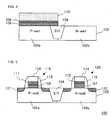
- FIG. 1is a cross-sectional view, illustrating a configuration of a semiconductor device in this embodiment.
- the semiconductor device 100is a complementary metal oxide semiconductor (CMOS) device including an N-type MOSFET 118 and a P-type MOSFET 120 .
- CMOScomplementary metal oxide semiconductor
- this CMOS devicecomposes an internal circuit of a LSI.
- the semiconductor device 100comprises a silicon substrate 102 , which has a P-well 102 a of P-type conductivity and an N-well 102 b of N-type conductivity provided thereon and a device separating-region 104 for separating the P-well 102 a from the N-well 102 b .
- An N-type MOSFET 118 and a P-type MOSFET 120are formed in the P-well 102 a and the N-well 102 b , respectively.
- a pair of impurity diffusion regions 121is provided in the P-well 102 a , and a channel region is formed therebetween.
- a gatewhich comprises a gate insulating film having a silicon oxide film 106 and a first high dielectric constant film 111 formed thereon in this sequence, a gate electrode provided on the gate insulating film and composed of a polycrystalline silicon film 114 and a side wall insulating film 115 .
- the polycrystalline silicon film 114is disposed so as to contact with the first high dielectric constant film 111 .
- the polycrystalline silicon film 114 of the N-type MOSFET 118is doped with an N-type impurity.
- the N-type MOSFET 118is constituted by these components.
- a pair of impurity diffusion regions 122is provided in the N-well 102 b , and a channel region is formed therebetween.
- a gatewhich comprises a gate insulating film having a silicon oxide film 106 and a second high dielectric constant film 112 formed thereon in this sequence, a gate electrode provided on the gate insulating film and composed of a polycrystalline silicon film 114 and a side wall insulating film 116 .
- the polycrystalline silicon film 114is disposed so as to contact with the second high dielectric constant film 112 .
- the polycrystalline silicon film 114 of the P-type MOSFET 120is doped with a P-type impurity.
- the P-type MOSFET 120is constituted by these components.
- the first high dielectric constant film 111 and the second high dielectric constant film 112are films having higher relative dielectric constant than silicon oxide, and so-called high-k film can be employed for these films.
- the first high dielectric constant film 111 and the second high dielectric constant film 112may be composed of a material having relative dielectric constant of equal to or higher than 10. More specifically, the first high dielectric constant film 111 and the second high dielectric constant film 112 may be composed of a material containing one or more element selected from a group consisting of Hf and Zr, respectively, and the available films may be an oxide film containing any of the above-described element, a silicate film or the like.
- the use of such materialsincreases the relative dielectric constants of the first high dielectric constant film 111 and the second high dielectric constant film 112 , while providing improved heat resistances. This feature can contribute a miniaturization and an improvement on the reliability of the MOSFET.
- the first high dielectric constant film 111 and the second high dielectric constant film 112may be composed of the same material or may be composed of different materials.
- the first high dielectric constant film 111 and the second high dielectric constant film 112may be composed of a material containing Hf and Si. In such case, the content ratio of Hf over the total content of Hf and Si can be equal to or higher than 20 atomic %.
- the first high dielectric constant film 111 and the second high dielectric constant film 112may be respectively and independently composed of HfSiO or HfAlO, or nitride thereof. In such case, a lower limit of the percentage of Hf for the total content of Hf and Al in HfAlO may be equal to or higher than 20 atomic %.
- the semiconductor devicesmay have a configuration, in which the first high dielectric constant film and the second high dielectric constant film are free of Al.
- the second high dielectric constant film 112 of the P-type MOSFET 120is formed to have the film thickness in the laminating direction, which is thinner than the film thickness of the first high dielectric constant film 111 of the N-type MOSFET 118 .
- film thicknessparticularly indicates the film thickness in the laminating direction.
- the P-type MOSFET 120In order to inhibit the increase of the gate leakage current in the N-type MOSFET 118 and to reduce the influence of Fermi level pinning to the P-type MOSFET 120 in the semiconductor device 100 comprising the N-type MOSFET 118 and the P-type MOSFET 120 , it is preferable to have a configuration, in which the relationship of the film thickness d 1 of the first high dielectric constant film 111 with the film thickness d 2 of the second high dielectric constant film 112 is presented as: d 1 /d 2 ⁇ 1.5.
- the film thickness of the first high dielectric constant film 111 of the N-type MOSFET 118may be, for example, equal to or larger than 1.5 nm. Having this configuration, the increase of the gate leakage current in the N-type MOSFET 118 can be inhibited. Further, while the upper limit thereof is not particularly limited, the upper limit thereof may be, for example, d 1 /d 2 ⁇ 3.
- the film thickness d 2 of the second high dielectric constant film 112 of the P-type MOSFET 120may be equal to or less than 1 nm, for example, and more preferably equal to or less than 0.5 nm. Having such configuration, influence of Fermi level pinning can be reduced.
- the materials containing the above-described elementsare employed for the materials composing the first high dielectric constant film 111 and the second high dielectric constant film 112 , a problem of increasing the threshold voltage may be occurred due to the influence of Fermi level pinning in the P-type MOSFET 120 .
- the second high dielectric constant film 112 in the P-type MOSFET 120is formed to have thinner film thickness according to the configuration of the semiconductor device 100 in the present embodiment, this can diminish the influence of Fermi level pinning.
- the first high dielectric constant film 111 of the N-type MOSFET 118is formed to have thicker film thickness, the increase of the gate leakage current can also be inhibited.
- the N-type MOSFET 118 and the P-type MOSFET 120can be typically formed to have substantially same film thickness in the laminating direction in the silicon oxide films 106 .
- FIGS. 2A to 2 D and FIGS. 3E to 3 Hare cross-sectional views, illustrating an example of a manufacturing procedure for the semiconductor device 100 having the configuration shown in FIG. 1 .
- an element-separating region 104is formed according to a shallow trench isolation (STI) in the silicon substrate 102 via a known technique, and thereafter, a P-type impurity is ion-implanted to form the P-well 102 a and an N-type impurity is ion-implanted to form the N-well 102 b , respectively ( FIG. 2A ).
- the element-separating region 104may be formed via other known methods such as, for example, local oxidation of silicon (LOCOS) method or the like.
- LOClocal oxidation of silicon
- channel regionsare formed in the P-well 102 a and the N-well 102 b , respectively, via a known technique.
- an N-type impurity and a P-type impuritycan be ion-implanted into the lower parts of the channel regions of the P-well 102 a and the N-well 102 b , respectively, to form punch through stop regions.
- the short-channel effect theretocan be inhibited by forming such punch through stop regions.
- a silicon oxide film 106(having film thickness of, e.g., 1 nm to 2 nm) is formed on the surface of the silicon substrate 102 ( FIG. 2B ).
- the silicon oxide film 106can be formed by, for example, conducting a thermal oxidation on the surface of the silicon substrate 102 .
- a condition for conducting the thermal oxidationmay be, for example, at a process temperature of 900 degree C. and for a duration time of on the order of from 40 to 50 seconds.
- a high dielectric constant film 108(having a film thickness of, e.g., about 1 nm) is formed on the silicon oxide film 106 ( FIG. 2C ).
- the high dielectric constant film 108may be deposited via a chemical vapor deposition (CVD), an atomic layer deposition (ALD) or the like.
- Hafnium silicateis employed for depositing the high dielectric constant film 108 in the present embodiment.
- the deposition thereofis conducted by using an organic hafnium source gas, an oxidizing gas and a silicon-containing gas.
- oxygenmay be employed for the oxidizing gas
- monosilane (SiH 4 )may be employed for the silicon-containing gas, for example.
- an annealingis carried out by using, for example, a nitrogen-containing gas such as ammonia.
- the processing condition thereofmay be, for example, at a process temperature of 900 to 1,000 degree C. and for a duration time of 40 seconds or the like.
- An unwanted crystallization of hafnium silicatecan be prevented by conducting the annealing process.
- a photo resist 110is formed on the P-well 102 a ( FIG. 2D ).
- the photo resist 110is formed by applying a resist over the surface of the high dielectric constant film 108 and then exposing and developing thereof through a mask for patterning (not shown). Then, a wet etching is carried out, by using, for example, diluted fluorinated acid (DHF). This procedure provides a selective removal of the high dielectric constant film 108 on the N-well 102 b .
- the photo resist 110is stripped under the dry atmosphere employing, for example, ozone, so as not to remove the high dielectric constant film 108 on the P-well 102 a ( FIG. 3E ).
- the second high dielectric constant film 112(having a film thickness of, e.g., about 0.7 nm) is formed on the high dielectric constant film 108 and the silicon oxide film 106 ( FIG. 3F ).
- the second high dielectric constant film 112can be formed similarly as in forming the high dielectric constant film 108 .
- the above-mentioned processprovides forming the high dielectric constant film on the P-well 102 a having thicker film thickness than the high dielectric constant film on the N-well 102 b.
- the polycrystalline silicon film 114is formed on the second high dielectric constant film 112 ( FIG. 3G ). Then, an N-type impurity is ion-implanted into the polycrystalline silicon film 114 deposited on the P-well 102 a , and a P-type impurity is ion-implanted into the polycrystalline silicon film 114 deposited on the N-well 102 b.
- the silicon oxide film 106 , the high dielectric constant film 108 , the second high dielectric constant film 112 and the polycrystalline silicon film 114are selectively dry-etched to form the shape of the gate electrode.
- a side wall insulating film 115is formed to cover the respective side walls of the silicon oxide film 106 , the high dielectric constant film 108 , the second high dielectric constant film 112 and the polycrystalline silicon film 114 .
- a side wall insulating film 116is formed to cover the respective side walls of the silicon oxide film 106 , the second high dielectric constant film 112 and the polycrystalline silicon film 114 ( FIG. 3H ).
- the side wall insulating film 115 and the side wall insulating film 116can be formed via an anisotropic etch process by using, for example, a fluorocarbon gas or the like. It is noted that the first high dielectric constant film 111 is composed of the high dielectric constant film 108 and the second high dielectric constant film 112 .
- source/drain extension regionswhich are electric connecting sections between the channel regions and the impurity diffusion regions described later, are formed on the surface of the P-well 102 a and the N-well 102 b , respectively.
- the outer layer of the P-well 102 ais doped with an N-type impurity such as P, As and the like through a mask of the gate electrode and the side wall insulating film 115 to form the impurity diffusion region 121 .
- the outer layer of the N-well 102 bis doped with a P-type impurity such as B, Al and the like through a mask of the gate electrode and the side wall insulating film 116 to form the impurity diffusion region 122 .
- the source region and the drain regionare formed according to this procedure.
- an activation of the doped impuritiesis carried out by thermally processing thereof within a non-oxidizing atmosphere.
- the semiconductor device 100which is the CMOS device, is formed by the above-mentioned process.
- quantity of a metal (Hf in this embodiment) diffusing into the polycrystalline silicon film 114 from the second high dielectric constant film 112can be reduced for the P-type MOSFET 120 , which is vulnerable by Fermi level pinning, by having thinner film thickness of the second high dielectric constant film 112 , thereby reducing the generation of the depletion layer in the polycrystalline silicon film 114 .
- Thiscan reduce the threshold voltage in the P-type MOSFET. Having such configuration, the threshold voltage in the P-type MOSFET can be controlled within a desired voltage range by adjusting a concentration of the impurity that is implanted into the silicon substrate.
- the N-type MOSFET 118a problem of increasing the gate leakage current is occurred, if the first high dielectric constant film 111 is provided to have thinner film thickness, similarly as in the second high dielectric constant film 112 .
- the film thickness of the first high dielectric constant film 111 of the N-type MOSFET 118can be controlled independently from the second high dielectric constant film 112 to provide the thicker film thickness than the thickness of the second high dielectric constant film 112 , and therefore the increase of the gate leakage current in the N-type MOSFET 118 is prevented.
- Fermi level pinning in the P-type MOSFET 120can be inhibited without increasing the gate leakage current in the N-type MOSFET 118 .
- the gate leakage current in the N-type MOSFET 118is not increased, thereby keeping the power consumption in the standby condition to a level equivalent to the conventional device.
- a wet etching processis conducted by using, for example, diluted fluorinated acid (DHF) to selectively remove the high dielectric constant film 108 and the silicon oxide film 106 on the N-well 102 b ( FIG. 4 ).
- DHFdiluted fluorinated acid
- the present embodimentis different from the first embodiment in the point that the silicon oxide film 106 is also removed with the high dielectric constant film 108 .
- the photo resist 110is removed and thereafter, a thermal oxidation is conducted on the surface of the N-well 102 b of the silicon substrate 102 to form a silicon oxide film (not shown) on the N-well 102 b .
- the high dielectric constant filmis formed on the silicon oxide film 106 and on the silicon oxide film disposed on the N-well 102 b .
- Such high dielectric constant filmcan be formed similarly as in the formation of the high dielectric constant film 108 .
- Film thickness of the silicon oxide film formed on the N-well 102 bmay be substantially same as the film thickness of the silicon oxide film 106 , or may be thinner or thicker than the film thickness of the silicon oxide film 106 .
- the film thickness of the silicon oxide film disposed on the N-well 102 bmay be substantially equal to a total film thickness of the film thickness of the silicon oxide film 106 and the high dielectric constant film 108 . Example of such situation is shown in FIG. 5 .
- the silicon oxide filmis formed on the N-well 102 b after removing the high dielectric constant film 108 according to the method for manufacturing the semiconductor device 100 in the present embodiment, there is no concern about generating a defect in the silicon oxide film when the high dielectric constant film 108 is etched off. Therefore, the high dielectric constant film 108 can be etched off under various conditions.
- the P-type MOSFET 120 described in the first embodiment and having the configuration shown in FIG. 1was employed to investigate a relationship of the film thickness of the second high dielectric constant film 112 with the threshold voltage in the P-type MOSFET 120 . The results thereof are shown in FIG. 6 .
- thicker film thickness of the second high dielectric constant film 112provides an increase of the threshold voltage in the P-type MOSFET 120 . It was exhibited that the threshold voltage was in a level that is applicable to the manufacturing application (not higher than about 0.5 V) when the film thickness of the second high dielectric constant film 112 was equal to or less than 1 nm. In addition, it was found that the increase of the threshold voltage could be more effectively controlled by providing the film thickness of the second high dielectric constant film 112 as not greater than 0.5 nm.
- the P-type MOSFETs 120 having different film thicknesses of the silicon oxide films 106were examined, and similar results were exhibited in all of the examinations.
- the high dielectric constant film 108 and the second high dielectric constant film 112may be formed of different materials, respectively, in the process described in the first embodiment in reference to FIGS. 2A to 2 D and FIGS. 3E to 3 H.
- the first high dielectric constant film 111 and the second high dielectric constant film 112 shown in FIG. 1may also have laminated structures comprising a plurality of high dielectric constant films having different compositions, respectively.
- the present inventionis not limited to Hf and Zr, but is applicable to an N-type MOSFET and a P-type MOSFET having a gate.
- the second high dielectric constant film 112may be formed only on the N-well 102 b while remaining the photo resist 110 .
- the film thickness of the high dielectric constant film 108can be adjusted to a thickness, which provides sufficiently lower gate leakage current in the N-type MOSFET 118 that will not cause any problem.
- the first high dielectric constant film 111 and the second high dielectric constant film 112can be formed via various types of processes.
- the high dielectric constant film 108may not be completely removed.
- the high dielectric constant film 108 on N-well 102 bmay be removed and simultaneously the silicon oxide film 106 on the N-well 102 b may also be partially removed. It is satisfactory in the present invention that the desired film thickness of the first high dielectric constant film 111 of the N-type MOSFET 118 and the desired film thickness of the second high dielectric constant film 112 of the P-type MOSFET 120 may be eventually attained, respectively.
Landscapes
- Metal-Oxide And Bipolar Metal-Oxide Semiconductor Integrated Circuits (AREA)
- Insulated Gate Type Field-Effect Transistor (AREA)
Abstract
Description
- This application is based on Japanese patent application NO. 2004-144652, the content of which is incorporated hereinto by reference.
- 1. Field of the Invention
- The present invention relates to a semiconductor device comprising an N-type metal oxide semiconductor field effect transistor (MOSFET) and a P-type MOSFET both containing high dielectric constant films.
- 2. Description of the Related Art
- In recent years, the utilization of a thin film having high dielectric constant called high-k as a component material for semiconductor devices is actively investigated. Typical high-k materials include oxides of elements such as Zr, Hf and the like. The use of such materials for a gate insulating film of a MOSFET reduces a silicon oxide-conversion electrical thickness, even though the physical thickness of the gate insulating film is increased to a certain level, thereby providing physically and structurally stable gate insulating films. Thus, both or either one of an increase of metal oxide semiconductor (MOS) capacity for enhancing MOSFET characteristics and a reduction of a gate leakage current as compared with a conventional case of employing silicon oxide can be achieved.
- Japanese Laid-open patent publication No. 2002-280,461 discloses a complementary metal oxide semiconductor (CMOS) device including an N-MOSFET and P-MOSFET employing such high-k material. The N-MOSFET and P-MOSFET include a gate insulating film composed of a low dielectric constant film such as silicon oxide and the like, and a high dielectric constant film and a gate electrode composed of polycrystalline silicon. The gate electrode is disposed so as to contact with the high dielectric constant film of the gate insulating film.
- However, a comprehension is obtained according to the recent study, in which a phenomenon called Fermi level pinning is caused when the gate insulating film is composed of a high-k film and the gate electrode is composed of a polycrystalline silicon (C. Hobbs et al., entitled “Fermi Level Pinning at the Poly Si/Metal Oxide Interface”, 2003 Symposium on VLSI Technology Digest of Technical Papers, 4-89114-035-6/03). It is considered that Fermi level pinning is caused when an energy level is created on the basis of chemical bonding of silicon with the above-described metal for composing the high-dielectric constant film diffusing through the polycrystalline silicon that composes the gate electrode, in vicinity of an interface on the side of the gate insulating film in the gate electrode.
- When the metal composing the high dielectric constant film is diffused in the polycrystalline silicon of the gate electrode of the MOSFET, a depletion layer is created in the gate polycrystalline silicon in vicinity of an interface thereof with the gate insulating film. Sufficient electrical field cannot be applied to the gate insulating film due to an influence of such depletion layer even though a gate voltage is applied, and thus it is difficult to induce enough amount of carrier in the channel region. As a result, a problem is arisen, in which a threshold voltage is increased, and further a fluctuation in the threshold voltage is also increased.
- Such Fermi level pinning is easy to be occurred in a P-type MOSFET that includes a gate electrode composed of a polycrystalline silicon containing P-type impurity, in particular in a case of employing Hf and/or Zr for the high dielectric constant film.
- In the meantime, high dielectric constant films having same composition and same film thickness are employed for gate insulating films of N-type MOSFET and P-type MOSFET, which respectively constitute internal circuits of LSI in conventional CMOS devices. In such case, a problem is occurred that the gate leakage current generated in the N-type MOSFET is higher than that generated in the P-type MOSFET in the CMOS device. Therefore, the gate leakage current in the N-type MOSFET is focused in view of power consumption design, and a high dielectric constant film having a suitable film thickness, which is capable of sufficiently reducing the gate leakage current to an acceptable level, is deposited.
- On the other hand, a threshold voltage for the P-type MOSFET employing a high dielectric constant film containing a specific element such as Hf, Zr and the like is increased to a level that is higher than that for the P-type MOSFET employing silicon oxide for the gate insulating film, for the reason stated above, and is eventually increased to a level that provides a difficult situation in establishing a desired threshold voltage by adjusting density of an impurity in the Si substrate.
- The present inventors have found in the process of examining measures to the above-described problem that a quantity of an increase of the threshold voltage is dependent on the film thickness of the high dielectric constant film. In addition, the present inventors also have found that the reason for causing the above-described problem is not from an increase of MOS capacity caused by the reduction of the thickness of the high dielectric constant film, but from the fact that a quantity of the specific element originally contained in high dielectric constant film diffusing from the high dielectric constant film to the gate electrode is dependent on the film thickness thereof, and thus being attained to invent the present invention.
- According to one aspect of the present invention, there is provided a semiconductor device, comprising: an N-type MOSFET including: a semiconductor substrate, a first gate insulating film, formed on the semiconductor substrate, and composed of a first high dielectric constant film containing one or more element(s) selected from a group consisting of Hf and Zr; and a first gate electrode, disposed on the first gate insulating film to contact with the first high dielectric constant film, and composed of a polycrystalline silicon film; and a P-type MOSFET including: a second gate insulating film, formed on the semiconductor substrate to be juxtaposed to the N-type MOSFET, and composed of a second high dielectric constant film containing one or more element(s) selected from a group consisting of Hf and Zr; and a second gate electrode, disposed on the second gate insulating film to contact with the second high dielectric constant film, and composed of a polycrystalline silicon film, wherein a film thickness of the second high dielectric constant film is less than a film thickness of the first high dielectric constant film.
- In the configuration described above, the first high dielectric constant film and the second high dielectric constant film may also be composed of a chemical compound of one or more element(s) selected from a group consisting of Hf and Zr and one or more element(s) selected from a group consisting of Si, O and N.
- The disclosure of C. Hobbs et al, entitled “Fermi Level Pinning at the Poly Si/Metal Oxide Interface”, 2003 Symposium on VLSI Technology Digest of Technical Papers describes that Fermi level pinning is caused when a high-k film such as HfO2and the like is provided so as to contact with a polycrystalline silicon. Such Fermi level pinning is considerably influential to the operation of the P-type MOSFET. In particular, the influence to the P-type MOSFET becomes larger when the P-type MOSFET includes the high dielectric constant film containing Hf such as HfO2and HfAlO. However, since the second high dielectric constant film in the P-type MOSFET is formed to have thinner film thickness in the present invention, the quantity of the metal, which is originally contained in the second high dielectric constant film and is diffused into the polycrystalline silicon film, is reduced, even though the second high dielectric constant film contacts with the polycrystalline silicon film, and thus the generation of the depletion layer in the polycrystalline silicon can be avoided. This can diminish the influence of Fermi level pinning to the P-type MOSFET. Therefore, the increase of the threshold voltage of the P-type MOSFET can be inhibited and the fluctuation thereof can also be reduced.
- In addition, the high dielectric constant film in the N-type MOSFET can be formed to have larger film thickness, and thus the enhancement of the gate leakage current, which is a problem for the N-type MOSFET, can be also inhibited.
- The semiconductor devices according to the above-described aspects of the present invention may further has a configuration, in which the first high dielectric constant film and the second high dielectric constant film may contain Hf and Si. In addition, in such case, a content ratio of Hf for the total content of Hf and Si may be equal to or higher than 20 atomic % in the first high dielectric constant film and the second high dielectric constant film. More preferably, the content ratio of Hf for the total content of Hf and Si may be equal to or higher than 30%. The semiconductor devices according to the above-described aspects of the present invention may further have a configuration, in which the first high dielectric constant film and the second high dielectric constant film may be respectively and independently composed of HfSiO or HfAlO, or nitride thereof. In such case, a lower limit of the percentage of Hf over the total content of Hf and Al in HfAlO may be equal to or higher than 20 atomic %. Further, the semiconductor devices may have a configuration, in which the first high dielectric constant film and the second high dielectric constant film are free of Al.
- The influence of Fermi level pinning in the P-type MOSFET may be a problem in the above-described cases. On the contrary, since the second high dielectric constant film in the P-type MOSFET is formed to have thinner film thickness in the present invention, this can diminish the influence of Fermi level pinning to the operation of the P-type MOSFET, as described above.
- The semiconductor devices according to the above-described aspects of the present invention may further have a configuration, in which the first gate insulating film of the N-type MOSFET further includes a silicon oxide film provided between the semiconductor substrate and the first high dielectric constant film, and the second gate insulating film of the P-type MOSFET further includes a silicon oxide film provided between the semiconductor substrate and the second high dielectric constant film. The silicon oxide film may include nitrogen.
- Diffusion, migration or the like of the metal contained in the first high dielectric constant film and the second high dielectric constant film into the semiconductor substrate can be prevented by providing the silicon oxide films between the semiconductor substrate and the first high dielectric constant film and between the semiconductor substrate and the second high dielectric constant film, respectively.
- The semiconductor devices according to the above-described aspects of the present invention may further have a configuration, in which, in the first gate electrode of the N-type MOSFET in the semiconductor device, the polycrystalline silicon film includes an N-type impurity, and in the second gate electrode of the P-type MOSFET, the polycrystalline silicon film includes a P-type impurity.
- Fermi level pinning described above is considerably caused when the polycrystalline silicon film containing P-type impurity contacts with the high dielectric constant film. On the contrary, since the second high dielectric constant film in the P-type MOSFET is formed to have thinner film thickness in the present invention, the quantity of the metal, which is originally contained in the second high dielectric constant film and is diffused into the polycrystalline silicon film, is reduced, even though the second high dielectric constant film contacts with the polycrystalline silicon film, and thus the generation of the depletion layer in the polycrystalline silicon can be avoided.
- The semiconductor devices according to the above-described aspects of the present invention may further have a configuration, in which a relationship of a film thickness d1 of the first high dielectric constant film with a film thickness d2 of the second high dielectric constant film is: d1/d2≧1.5. Further, while the upper limit thereof is not particularly limited, the upper limit thereof may be, for example, d1/d2≦3.
- The influence of Fermi level pinning can be moderated to reduce the threshold voltage and the increase of the gate leakage current can be inhibited by providing such relationship between the film thickness of the first high dielectric constant film and the film thickness of the second high dielectric constant film. When the first high dielectric constant film is composed of, for example, HfSiNO, the film thickness d1 may be equal to or higher than 1.5 nm. Having this configuration, the increase of the gate leakage current in the N-type MOSFET can be inhibited. In addition, the film thickness d2 of the second high dielectric constant film may be equal to or less than 1 nm, for example, and more preferably equal to or less than 0.5 nm. Having such configuration, the influence of Fermi level pinning can be reduced.
- The semiconductor devices according to the above-described aspects of the present invention may further have a configuration, in which the N-type MOSFET and the P-type MOSFET compose internal circuits of LSI.
- According to another aspect of the present invention, there is provided a method for manufacturing a semiconductor device including an N-type MOSFET and a P-type MOSFET, comprising: forming on an entire surface of a semiconductor substrate a first layer composed of a high dielectric constant material including one or more element(s) selected from a group consisting of Hf and Zr, said semiconductor substrate being provided with a P-well and an N-well that are juxtaposed; covering said first layer on said P-well with a protective film; selectively removing said first layer on said N-well through a mask of said protective film; forming on at least said N-well a second layer composed of a high dielectric constant material including one or more element(s) selected from a group consisting of Hf and Zr; forming a polycrystalline silicon film on said first layer and said second layer; selectively removing said first layer, said second layer and said polycrystalline silicon film to form the layers into a shape of a gate electrode, wherein said second layer is formed in said forming said second layer to provide a total film thickness of said first layer and said second layer on said N-well, which is thinner than a total film thickness of said first layer and said second layer on said P-well.
- In such aspect of the present invention, the first layer and the second layer may also be composed of a chemical compound of one or more element (s) selected from a group consisting of Hf and Zr and one or more element(s) selected from a group consisting of Si, O and N.
- The method for manufacturing the semiconductor devices according to the above-described aspect of the present invention may further have a configuration, in which the method further comprises, before forming the first layer, forming a silicon oxide film on the entire surface of the semiconductor substrate, wherein the first layer is formed on the silicon oxide film in the forming the first layer. The silicon oxide film may contain nitrogen.
- The method for manufacturing the semiconductor devices according to the above-described aspect of the present invention may further have a configuration, in which the first layer and the second layer contain Hf and Si.
- The method for manufacturing the semiconductor devices according to the above-described aspect of the present invention may further have a configuration, in which a content ratio of Hf for total content of Hf and Si is equal to or higher than 20% in said first layer and said second layer.
- The method for manufacturing the semiconductor devices according to the above-described aspect of the present invention may further have a configuration, in which the first layer and said second layer are respectively and independently composed of HfSiO or HfAlO, or nitride thereof. In such case, a lower limit of the percentage of Hf over the total content of Hf and Al in HfAlO may be equal to or higher than 20 atomic %.
- Further, the semiconductor devices may have a configuration, in which the first high dielectric constant film and the second high dielectric constant film are free of Al.
- According to the present invention, the controllability of the threshold voltage of the P-type MOSFET within an desired range by reducing the threshold voltage of the P-type MOSFET is provided while preventing an increase of the gate leakage current in N-type MOSFET for the semiconductor device that comprises the N-type MOSFET and P-type MOSFET including high dielectric constant films.
- The above and other objects, advantages and features of the present invention will be more apparent from the following description taken in conjunction with the accompanying drawings, in which:
FIG. 1 is a cross-sectional view of an exemplary configuration of a semiconductor device in an embodiment of the present invention;FIGS. 2A to2D are cross-sectional views of the semiconductor device, illustrating an exemplary manufacturing procedure of the semiconductor device in the embodiment of the present invention;FIGS. 3E to3H are cross-sectional views of the semiconductor device, illustrating an exemplary manufacturing procedure of the semiconductor device in the embodiment of the present invention;FIG. 4 is a cross-sectional view of the semiconductor device, illustrating an intermediate stage in the manufacturing procedure of the semiconductor device in the embodiment of the present invention;FIG. 5 is a cross-sectional view of the semiconductor device, illustrating an exemplary configuration of a semiconductor device in an embodiment of the present invention; andFIG. 6 is a graph showing a relationship of the threshold voltage over the film thickness of the high dielectric constant film in the P-type MOSFET.- The invention will be now described herein with reference to illustrative embodiments. Those skilled in the art will recognize that many alternative embodiments can be accomplished using the teachings of the present invention and that the invention is not limited to the embodiments illustrated for explanatory purposed.
- Preferable embodiments according to the present invention will be described as follows in further detail, in reference to the annexed figures. In all figures, identical numeral is assigned to an element commonly appeared in the figures, and the detailed description thereof will not be presented.
FIG. 1 is a cross-sectional view, illustrating a configuration of a semiconductor device in this embodiment.- In this embodiment, the
semiconductor device 100 is a complementary metal oxide semiconductor (CMOS) device including an N-type MOSFET 118 and a P-type MOSFET 120. In addition, this CMOS device composes an internal circuit of a LSI. - The
semiconductor device 100 comprises asilicon substrate 102, which has a P-well102aof P-type conductivity and an N-well102bof N-type conductivity provided thereon and a device separating-region 104 for separating the P-well102afrom the N-well102b. An N-type MOSFET 118 and a P-type MOSFET 120 are formed in the P-well102aand the N-well102b, respectively. - A pair of
impurity diffusion regions 121 is provided in the P-well102a, and a channel region is formed therebetween. On the channel region is provided with a gate, which comprises a gate insulating film having asilicon oxide film 106 and a first high dielectricconstant film 111 formed thereon in this sequence, a gate electrode provided on the gate insulating film and composed of apolycrystalline silicon film 114 and a sidewall insulating film 115. Here, thepolycrystalline silicon film 114 is disposed so as to contact with the first high dielectricconstant film 111. Thepolycrystalline silicon film 114 of the N-type MOSFET 118 is doped with an N-type impurity. The N-type MOSFET 118 is constituted by these components. - Similarly, a pair of
impurity diffusion regions 122 is provided in the N-well102b, and a channel region is formed therebetween. On the channel region is provided with a gate, which comprises a gate insulating film having asilicon oxide film 106 and a second high dielectricconstant film 112 formed thereon in this sequence, a gate electrode provided on the gate insulating film and composed of apolycrystalline silicon film 114 and a sidewall insulating film 116. Here, thepolycrystalline silicon film 114 is disposed so as to contact with the second high dielectricconstant film 112. Thepolycrystalline silicon film 114 of the P-type MOSFET 120 is doped with a P-type impurity. The P-type MOSFET 120 is constituted by these components. - The first high dielectric
constant film 111 and the second high dielectricconstant film 112 are films having higher relative dielectric constant than silicon oxide, and so-called high-k film can be employed for these films. The first high dielectricconstant film 111 and the second high dielectricconstant film 112 may be composed of a material having relative dielectric constant of equal to or higher than 10. More specifically, the first high dielectricconstant film 111 and the second high dielectricconstant film 112 may be composed of a material containing one or more element selected from a group consisting of Hf and Zr, respectively, and the available films may be an oxide film containing any of the above-described element, a silicate film or the like. The use of such materials increases the relative dielectric constants of the first high dielectricconstant film 111 and the second high dielectricconstant film 112, while providing improved heat resistances. This feature can contribute a miniaturization and an improvement on the reliability of the MOSFET. The first high dielectricconstant film 111 and the second high dielectricconstant film 112 may be composed of the same material or may be composed of different materials. - The first high dielectric
constant film 111 and the second high dielectricconstant film 112 may be composed of a material containing Hf and Si. In such case, the content ratio of Hf over the total content of Hf and Si can be equal to or higher than 20 atomic %. In addition, the first high dielectricconstant film 111 and the second high dielectricconstant film 112 may be respectively and independently composed of HfSiO or HfAlO, or nitride thereof. In such case, a lower limit of the percentage of Hf for the total content of Hf and Al in HfAlO may be equal to or higher than 20 atomic %. Further, the semiconductor devices may have a configuration, in which the first high dielectric constant film and the second high dielectric constant film are free of Al. - In the present embodiment, the second high dielectric
constant film 112 of the P-type MOSFET 120 is formed to have the film thickness in the laminating direction, which is thinner than the film thickness of the first high dielectricconstant film 111 of the N-type MOSFET 118. Hereinafter, a simple statement as “film thickness” particularly indicates the film thickness in the laminating direction. In order to inhibit the increase of the gate leakage current in the N-type MOSFET 118 and to reduce the influence of Fermi level pinning to the P-type MOSFET 120 in thesemiconductor device 100 comprising the N-type MOSFET 118 and the P-type MOSFET 120, it is preferable to have a configuration, in which the relationship of the film thickness d1 of the first high dielectricconstant film 111 with the film thickness d2 of the second high dielectricconstant film 112 is presented as: d1/d2≧1.5. - The film thickness of the first high dielectric
constant film 111 of the N-type MOSFET 118 may be, for example, equal to or larger than 1.5 nm. Having this configuration, the increase of the gate leakage current in the N-type MOSFET 118 can be inhibited. Further, while the upper limit thereof is not particularly limited, the upper limit thereof may be, for example, d1/d2≦3. The film thickness d2 of the second high dielectricconstant film 112 of the P-type MOSFET 120 may be equal to or less than 1 nm, for example, and more preferably equal to or less than 0.5 nm. Having such configuration, influence of Fermi level pinning can be reduced. - When the materials containing the above-described elements are employed for the materials composing the first high dielectric
constant film 111 and the second high dielectricconstant film 112, a problem of increasing the threshold voltage may be occurred due to the influence of Fermi level pinning in the P-type MOSFET 120. However, since the second high dielectricconstant film 112 in the P-type MOSFET 120 is formed to have thinner film thickness according to the configuration of thesemiconductor device 100 in the present embodiment, this can diminish the influence of Fermi level pinning. On the other hand, since the first high dielectricconstant film 111 of the N-type MOSFET 118 is formed to have thicker film thickness, the increase of the gate leakage current can also be inhibited. - Although it is not intended to particularly limit the scope of the invention, the N-
type MOSFET 118 and the P-type MOSFET 120 can be typically formed to have substantially same film thickness in the laminating direction in thesilicon oxide films 106. FIGS. 2A to2D andFIGS. 3E to3H are cross-sectional views, illustrating an example of a manufacturing procedure for thesemiconductor device 100 having the configuration shown inFIG. 1 .- At first, an element-separating
region 104 is formed according to a shallow trench isolation (STI) in thesilicon substrate 102 via a known technique, and thereafter, a P-type impurity is ion-implanted to form the P-well102aand an N-type impurity is ion-implanted to form the N-well102b, respectively (FIG. 2A ). The element-separatingregion 104 may be formed via other known methods such as, for example, local oxidation of silicon (LOCOS) method or the like. - Subsequently, channel regions are formed in the P-well102aand the N-well102b, respectively, via a known technique. Here, an N-type impurity and a P-type impurity can be ion-implanted into the lower parts of the channel regions of the P-well102aand the N-well102b, respectively, to form punch through stop regions. The short-channel effect thereto can be inhibited by forming such punch through stop regions.
- Subsequently, a silicon oxide film106 (having film thickness of, e.g., 1 nm to 2 nm) is formed on the surface of the silicon substrate102 (
FIG. 2B ). Thesilicon oxide film 106 can be formed by, for example, conducting a thermal oxidation on the surface of thesilicon substrate 102. A condition for conducting the thermal oxidation may be, for example, at a process temperature of 900 degree C. and for a duration time of on the order of from 40 to 50 seconds. - Subsequently, a high dielectric constant film108 (having a film thickness of, e.g., about 1 nm) is formed on the silicon oxide film106 (
FIG. 2C ). The high dielectricconstant film 108 may be deposited via a chemical vapor deposition (CVD), an atomic layer deposition (ALD) or the like. Hafnium silicate is employed for depositing the high dielectricconstant film 108 in the present embodiment. The deposition thereof is conducted by using an organic hafnium source gas, an oxidizing gas and a silicon-containing gas. Here, oxygen may be employed for the oxidizing gas and monosilane (SiH4) may be employed for the silicon-containing gas, for example. - Thereafter, an annealing is carried out by using, for example, a nitrogen-containing gas such as ammonia. The processing condition thereof may be, for example, at a process temperature of 900 to 1,000 degree C. and for a duration time of 40 seconds or the like. An unwanted crystallization of hafnium silicate can be prevented by conducting the annealing process.
- Subsequently, a photo resist110 is formed on the P-well102a(
FIG. 2D ). The photo resist110 is formed by applying a resist over the surface of the high dielectricconstant film 108 and then exposing and developing thereof through a mask for patterning (not shown). Then, a wet etching is carried out, by using, for example, diluted fluorinated acid (DHF). This procedure provides a selective removal of the high dielectricconstant film 108 on the N-well102b. Subsequently, the photo resist110 is stripped under the dry atmosphere employing, for example, ozone, so as not to remove the high dielectricconstant film 108 on the P-well102a(FIG. 3E ). - Then, the second high dielectric constant film112 (having a film thickness of, e.g., about 0.7 nm) is formed on the high dielectric
constant film 108 and the silicon oxide film106 (FIG. 3F ). The second high dielectricconstant film 112 can be formed similarly as in forming the high dielectricconstant film 108. The above-mentioned process provides forming the high dielectric constant film on the P-well102ahaving thicker film thickness than the high dielectric constant film on the N-well102b. - Thereafter, the
polycrystalline silicon film 114 is formed on the second high dielectric constant film112 (FIG. 3G ). Then, an N-type impurity is ion-implanted into thepolycrystalline silicon film 114 deposited on the P-well102a, and a P-type impurity is ion-implanted into thepolycrystalline silicon film 114 deposited on the N-well102b. - Subsequently, the
silicon oxide film 106, the high dielectricconstant film 108, the second high dielectricconstant film 112 and thepolycrystalline silicon film 114 are selectively dry-etched to form the shape of the gate electrode. Then, on the P-well102a, a sidewall insulating film 115 is formed to cover the respective side walls of thesilicon oxide film 106, the high dielectricconstant film 108, the second high dielectricconstant film 112 and thepolycrystalline silicon film 114. Similarly, on the N-well102b, a sidewall insulating film 116 is formed to cover the respective side walls of thesilicon oxide film 106, the second high dielectricconstant film 112 and the polycrystalline silicon film114 (FIG. 3H ). The sidewall insulating film 115 and the sidewall insulating film 116 can be formed via an anisotropic etch process by using, for example, a fluorocarbon gas or the like. It is noted that the first high dielectricconstant film 111 is composed of the high dielectricconstant film 108 and the second high dielectricconstant film 112. - Subsequently, source/drain extension regions, which are electric connecting sections between the channel regions and the impurity diffusion regions described later, are formed on the surface of the P-well102aand the N-well102b, respectively.
- Next, concerning the surface of the P-well102a, the outer layer of the P-well102ais doped with an N-type impurity such as P, As and the like through a mask of the gate electrode and the side
wall insulating film 115 to form theimpurity diffusion region 121. Similarly, concerning the surface of the N-well102b, the outer layer of the N-well102bis doped with a P-type impurity such as B, Al and the like through a mask of the gate electrode and the sidewall insulating film 116 to form theimpurity diffusion region 122. The source region and the drain region are formed according to this procedure. Thereafter, an activation of the doped impurities is carried out by thermally processing thereof within a non-oxidizing atmosphere. Thesemiconductor device 100, which is the CMOS device, is formed by the above-mentioned process. - In this embodiment, quantity of a metal (Hf in this embodiment) diffusing into the
polycrystalline silicon film 114 from the second high dielectricconstant film 112 can be reduced for the P-type MOSFET 120, which is vulnerable by Fermi level pinning, by having thinner film thickness of the second high dielectricconstant film 112, thereby reducing the generation of the depletion layer in thepolycrystalline silicon film 114. This can reduce the threshold voltage in the P-type MOSFET. Having such configuration, the threshold voltage in the P-type MOSFET can be controlled within a desired voltage range by adjusting a concentration of the impurity that is implanted into the silicon substrate. On the other hand, in the N-type MOSFET 118, a problem of increasing the gate leakage current is occurred, if the first high dielectricconstant film 111 is provided to have thinner film thickness, similarly as in the second high dielectricconstant film 112. However, in this embodiment, the film thickness of the first high dielectricconstant film 111 of the N-type MOSFET 118 can be controlled independently from the second high dielectricconstant film 112 to provide the thicker film thickness than the thickness of the second high dielectricconstant film 112, and therefore the increase of the gate leakage current in the N-type MOSFET 118 is prevented. As such, according to thesemiconductor device 100 in the present embodiment, Fermi level pinning in the P-type MOSFET 120 can be inhibited without increasing the gate leakage current in the N-type MOSFET 118. In addition, according to thesemiconductor device 100 in the present embodiment, the gate leakage current in the N-type MOSFET 118 is not increased, thereby keeping the power consumption in the standby condition to a level equivalent to the conventional device. - In this embodiment, similar process as described in the first embodiment in reference to
FIG. 2A toFIG. 2D is conducted, and more specifically thesilicon oxide film 106 and the high dielectricconstant film 108 are formed on thesilicon substrate 102 and the photo resist110 is formed over the P-well102a. A wet etching process is conducted by using, for example, diluted fluorinated acid (DHF) to selectively remove the high dielectricconstant film 108 and thesilicon oxide film 106 on the N-well102b(FIG. 4 ). The present embodiment is different from the first embodiment in the point that thesilicon oxide film 106 is also removed with the high dielectricconstant film 108. - Subsequently, the photo resist110 is removed and thereafter, a thermal oxidation is conducted on the surface of the N-well102bof the
silicon substrate 102 to form a silicon oxide film (not shown) on the N-well102b. Subsequently, the high dielectric constant film is formed on thesilicon oxide film 106 and on the silicon oxide film disposed on the N-well102b. Such high dielectric constant film can be formed similarly as in the formation of the high dielectricconstant film 108. - Film thickness of the silicon oxide film formed on the N-well102bmay be substantially same as the film thickness of the
silicon oxide film 106, or may be thinner or thicker than the film thickness of thesilicon oxide film 106. - For example, the film thickness of the silicon oxide film disposed on the N-well102bmay be substantially equal to a total film thickness of the film thickness of the
silicon oxide film 106 and the high dielectricconstant film 108. Example of such situation is shown inFIG. 5 . - Since the silicon oxide film is formed on the N-well102bafter removing the high dielectric
constant film 108 according to the method for manufacturing thesemiconductor device 100 in the present embodiment, there is no concern about generating a defect in the silicon oxide film when the high dielectricconstant film 108 is etched off. Therefore, the high dielectricconstant film 108 can be etched off under various conditions. - The P-
type MOSFET 120 described in the first embodiment and having the configuration shown inFIG. 1 was employed to investigate a relationship of the film thickness of the second high dielectricconstant film 112 with the threshold voltage in the P-type MOSFET 120. The results thereof are shown inFIG. 6 . - As can be seen in the graph, thicker film thickness of the second high dielectric
constant film 112 provides an increase of the threshold voltage in the P-type MOSFET 120. It was exhibited that the threshold voltage was in a level that is applicable to the manufacturing application (not higher than about 0.5 V) when the film thickness of the second high dielectricconstant film 112 was equal to or less than 1 nm. In addition, it was found that the increase of the threshold voltage could be more effectively controlled by providing the film thickness of the second high dielectricconstant film 112 as not greater than 0.5 nm. The P-type MOSFETs 120 having different film thicknesses of thesilicon oxide films 106 were examined, and similar results were exhibited in all of the examinations. - On the other hand, it was also indicated that the influence of the gate leakage current is reduced when the film thickness of the first high dielectric
constant film 111 in the N-type MOSFET 118 is equal to or greater than 1.5 nm, although it is not shown in this graph. - It was found from the above-mentioned results that both of the influence of the gate leakage current and the influence of Fermi level pinning in the CMOS device can be reduced when the relationship of the film thickness d1 of the first high dielectric
constant film 111 with the film thickness d2 of the second high dielectricconstant film 112 is presented as: d1/d2≧1.5. - While the preferred embodiments of the present invention have been described above in reference to the annexed figures, it should be understood that the disclosures above are presented for the purpose of illustrating the present invention, and various configurations other than the above-described configurations can also be adopted.
- For example, while the configuration employing the hafnium silicate film as the high dielectric constant film is described in the above-described embodiment, in addition thereto, oxide film of Hf, Zr or the like, silicate film of Hf, Zr or the like, oxynitride film of Hf, Zr or the like can similarly be employed. Further, the high dielectric
constant film 108 and the second high dielectricconstant film 112 maybe formed of different materials, respectively, in the process described in the first embodiment in reference toFIGS. 2A to2D andFIGS. 3E to3H. Moreover, the first high dielectricconstant film 111 and the second high dielectricconstant film 112 shown inFIG. 1 may also have laminated structures comprising a plurality of high dielectric constant films having different compositions, respectively. - Further, the present invention is not limited to Hf and Zr, but is applicable to an N-type MOSFET and a P-type MOSFET having a gate. insulating film containing an element, which may otherwise be diffused into the polycrystalline silicon film as being contacted with the polycrystalline silicon film to possibly cause Fermi level pinning.
- While it was described that the photo resist110 is removed in the process described in reference to
FIG. 3E in the first embodiment and the second high dielectricconstant film 112 is formed on the P-well102ain the process described in reference toFIG. 3F , the second high dielectricconstant film 112 may be formed only on the N-well102bwhile remaining the photo resist110. In this case, the film thickness of the high dielectricconstant film 108 can be adjusted to a thickness, which provides sufficiently lower gate leakage current in the N-type MOSFET 118 that will not cause any problem. As such, the first high dielectricconstant film 111 and the second high dielectricconstant film 112 can be formed via various types of processes. - While a configuration of removing the high dielectric
constant film 108 on the N-well102bin the process described in reference toFIG. 3E is described in the first embodiment, the high dielectricconstant film 108 may not be completely removed. In addition, the high dielectricconstant film 108 on N-well102bmay be removed and simultaneously thesilicon oxide film 106 on the N-well102bmay also be partially removed. It is satisfactory in the present invention that the desired film thickness of the first high dielectricconstant film 111 of the N-type MOSFET 118 and the desired film thickness of the second high dielectricconstant film 112 of the P-type MOSFET 120 may be eventually attained, respectively. - It is apparent that the present invention is not limited to the above embodiment, that may be modified and changed without departing from the scope and spirit of the invention.
Claims (8)
Applications Claiming Priority (2)
| Application Number | Priority Date | Filing Date | Title |
|---|---|---|---|
| JP2004144652AJP4040602B2 (en) | 2004-05-14 | 2004-05-14 | Semiconductor device |
| JP2004-144652 | 2004-05-14 |
Publications (2)
| Publication Number | Publication Date |
|---|---|
| US20050253181A1true US20050253181A1 (en) | 2005-11-17 |
| US7759744B2 US7759744B2 (en) | 2010-07-20 |
Family
ID=35308588
Family Applications (1)
| Application Number | Title | Priority Date | Filing Date |
|---|---|---|---|
| US11/129,440Active2026-06-22US7759744B2 (en) | 2004-05-14 | 2005-05-16 | Semiconductor device having high dielectric constant layers of different thicknesses |
Country Status (3)
| Country | Link |
|---|---|
| US (1) | US7759744B2 (en) |
| JP (1) | JP4040602B2 (en) |
| CN (1) | CN100461416C (en) |
Cited By (4)
| Publication number | Priority date | Publication date | Assignee | Title |
|---|---|---|---|---|
| US20070090471A1 (en)* | 2005-10-26 | 2007-04-26 | International Business Machines Corporation | Low threshold voltage semiconductor device with dual threshold voltage control means |
| US20090146215A1 (en)* | 2007-12-07 | 2009-06-11 | Hisashi Ogawa | Semiconductor device and method for fabricating the same |
| US20090206417A1 (en)* | 2008-02-20 | 2009-08-20 | Interuniversitair Microelektornica Centrum Vzw (Imec) | Semiconductor device and method for fabricating the same |
| US10714486B2 (en)* | 2018-09-13 | 2020-07-14 | Sandisk Technologies Llc | Static random access memory cell employing n-doped PFET gate electrodes and methods of manufacturing the same |
Families Citing this family (5)
| Publication number | Priority date | Publication date | Assignee | Title |
|---|---|---|---|---|
| JP4938262B2 (en)* | 2004-08-25 | 2012-05-23 | ルネサスエレクトロニクス株式会社 | Semiconductor device and manufacturing method thereof |
| US7518145B2 (en)* | 2007-01-25 | 2009-04-14 | International Business Machines Corporation | Integrated multiple gate dielectric composition and thickness semiconductor chip and method of manufacturing the same |
| JP2009027083A (en)* | 2007-07-23 | 2009-02-05 | Toshiba Corp | Semiconductor device and manufacturing method thereof |
| CN104952734B (en)* | 2015-07-16 | 2020-01-24 | 矽力杰半导体技术(杭州)有限公司 | Semiconductor structure and method of making the same |
| KR102328279B1 (en)* | 2017-08-11 | 2021-11-17 | 삼성전자주식회사 | A semiconductor device |
Citations (52)
| Publication number | Priority date | Publication date | Assignee | Title |
|---|---|---|---|---|
| US5480828A (en)* | 1994-09-30 | 1996-01-02 | Taiwan Semiconductor Manufacturing Corp. Ltd. | Differential gate oxide process by depressing or enhancing oxidation rate for mixed 3/5 V CMOS process |
| US5650958A (en)* | 1996-03-18 | 1997-07-22 | International Business Machines Corporation | Magnetic tunnel junctions with controlled magnetic response |
| US5859249A (en)* | 1997-02-19 | 1999-01-12 | Takasago International Corporation | 2-phenyl-2-(2'-piperidinylidene)acetate derivative, process for manufacturing the same, and process for manufacturing optically active 2-phenyl-2-(2'-piperidinyl)acetate derivative by asymmetrically hydrogenating the same |
| US5949707A (en)* | 1996-09-06 | 1999-09-07 | Nonvolatile Electronics, Incorporated | Giant magnetoresistive effect memory cell |
| US6107134A (en)* | 1998-05-26 | 2000-08-22 | Etron Technology, Inc. | High performance DRAM structure employing multiple thickness gate oxide |
| US6159799A (en)* | 1998-12-01 | 2000-12-12 | Hyundai Electronics Industries Co., Ltd. | Method of manufacturing semiconductor device comprising high voltage regions and floating gates |
| US6255698B1 (en)* | 1999-04-28 | 2001-07-03 | Advanced Micro Devices, Inc. | Separately optimized gate structures for n-channel and p-channel transistors in an integrated circuit |
| US6261978B1 (en)* | 1999-02-22 | 2001-07-17 | Motorola, Inc. | Process for forming semiconductor device with thick and thin films |
| US6346445B1 (en)* | 2000-11-17 | 2002-02-12 | United Microelectronics Corp. | Method for fabricating semiconductor devices with dual gate oxides |
| US6392922B1 (en)* | 2000-08-14 | 2002-05-21 | Micron Technology, Inc. | Passivated magneto-resistive bit structure and passivation method therefor |
| US6436771B1 (en)* | 2001-07-12 | 2002-08-20 | Taiwan Semiconductor Manufacturing Company | Method of forming a semiconductor device with multiple thickness gate dielectric layers |
| US6445554B1 (en)* | 2000-03-10 | 2002-09-03 | Read-Rite Corporation | Method and system for providing edge-junction TMR for high areal density magnetic recording |
| US6486682B1 (en)* | 2001-05-18 | 2002-11-26 | Advanced Micro Devices, Inc. | Determination of dielectric constants of thin dielectric materials in a MOS (metal oxide semiconductor) stack |
| US20030015763A1 (en)* | 2001-07-18 | 2003-01-23 | Matsushita Electric Industrial Co., Ltd. | Semiconductor device and method for manufacturing the same |
| US20030035254A1 (en)* | 2000-11-08 | 2003-02-20 | Akio Furukawa | Magnetic head using magneto-resistive effect and a manufacturing method thereof |
| US6541321B1 (en)* | 2002-05-14 | 2003-04-01 | Advanced Micro Devices, Inc. | Method of making transistors with gate insulation layers of differing thickness |
| US20030062586A1 (en)* | 2001-09-28 | 2003-04-03 | Wallace Robert M. | Gate structure and method |
| US6573134B2 (en)* | 2001-03-27 | 2003-06-03 | Sharp Laboratories Of America, Inc. | Dual metal gate CMOS devices and method for making the same |
| US6583013B1 (en)* | 1998-11-30 | 2003-06-24 | Texas Instruments Incorporated | Method for forming a mixed voltage circuit having complementary devices |
| US20030148625A1 (en)* | 2002-02-01 | 2003-08-07 | Ho Hsieh Yue | Method for wet etching of high k thin film at low temperature |
| US20030173586A1 (en)* | 2001-04-02 | 2003-09-18 | Masaru Moriwaki | Semiconductor device and method for manufacture thereof |
| US6624987B1 (en)* | 1999-05-31 | 2003-09-23 | Nec Corporation | Magnetic head with a tunnel junction including metallic material sandwiched between one of an oxide and a nitride of the metallic material |
| US6627932B1 (en)* | 2002-04-11 | 2003-09-30 | Micron Technology, Inc. | Magnetoresistive memory device |
| US20030186652A1 (en)* | 2000-08-17 | 2003-10-02 | Hopf Bernd Peter | System and method for transmitting signals in vehicles |
| US20030183939A1 (en)* | 2002-03-28 | 2003-10-02 | Fujitsu Limited | Semiconductor device with copper wirings |
| US20030222296A1 (en)* | 2002-06-04 | 2003-12-04 | Applied Materials, Inc. | Method of forming a capacitor using a high K dielectric material |
| US6670248B1 (en)* | 2002-08-07 | 2003-12-30 | Chartered Semiconductor Manufacturing Ltd. | Triple gate oxide process with high-k gate dielectric |
| US6669983B2 (en)* | 2001-10-25 | 2003-12-30 | Tdk Corporation | Manufacturing method of thin-film magnetic head with magnetoresistive effect element |
| US6686298B1 (en)* | 2000-06-22 | 2004-02-03 | Micron Technology, Inc. | Methods of forming structures over semiconductor substrates, and methods of forming transistors associated with semiconductor substrates |
| US20040023478A1 (en)* | 2002-07-31 | 2004-02-05 | Samavedam Srikanth B. | Capped dual metal gate transistors for CMOS process and method for making the same |
| US6700759B1 (en)* | 2000-06-02 | 2004-03-02 | Western Digital (Fremont), Inc. | Narrow track width magnetoresistive sensor and method of making |
| US6723658B2 (en)* | 2002-07-15 | 2004-04-20 | Texas Instruments Incorporated | Gate structure and method |
| US6734527B1 (en)* | 2002-12-12 | 2004-05-11 | Advanced Micro Devices, Inc. | CMOS devices with balanced drive currents based on SiGe |
| US20040105195A1 (en)* | 2002-11-29 | 2004-06-03 | Fontana Robert E. | Spin valve transistor with stabilization and method for producing the same |
| US20040105194A1 (en)* | 2002-11-29 | 2004-06-03 | Fontana Robert E. | Spin valve transistor with stabilization and method for producing the same |
| US20040124476A1 (en)* | 2002-11-14 | 2004-07-01 | Kiyotaka Miyano | Semiconductor device and method of manufacturing the same |
| US6759263B2 (en)* | 2002-08-29 | 2004-07-06 | Chentsau Ying | Method of patterning a layer of magnetic material |
| US6759081B2 (en)* | 2001-05-11 | 2004-07-06 | Asm International, N.V. | Method of depositing thin films for magnetic heads |
| US6784311B2 (en)* | 2000-02-22 | 2004-08-31 | Lonza Ag | Method of producing 3-aminoalkanoic acid esters |
| US6806127B2 (en)* | 2002-12-03 | 2004-10-19 | Freescale Semiconductor, Inc. | Method and structure for contacting an overlying electrode for a magnetoelectronics element |
| US6884887B1 (en)* | 1999-07-17 | 2005-04-26 | Degussa Ag | Method for producing amines by homogeneously catalyzed reductive amination of carbonyl compounds |
| US6897095B1 (en)* | 2004-05-12 | 2005-05-24 | Freescale Semiconductor, Inc. | Semiconductor process and integrated circuit having dual metal oxide gate dielectric with single metal gate electrode |
| US20050127417A1 (en)* | 2003-12-10 | 2005-06-16 | Saenger Katherine L. | Field effect transistor with etched-back gate dielectric |
| US6919251B2 (en)* | 2002-07-31 | 2005-07-19 | Texas Instruments Incorporated | Gate dielectric and method |
| US20050233562A1 (en)* | 2004-04-19 | 2005-10-20 | Adetutu Olubunmi O | Method for forming a gate electrode having a metal |
| US6967130B2 (en)* | 2003-06-20 | 2005-11-22 | Taiwan Semiconductor Manufacturing Company, Ltd. | Method of forming dual gate insulator layers for CMOS applications |
| US7018902B2 (en)* | 2001-11-30 | 2006-03-28 | Texas Instruments Incorporated | Gate dielectric and method |
| US7023049B2 (en)* | 2003-06-30 | 2006-04-04 | Kabushiki Kaisha Toshiba | Semiconductor device including nonvolatile memory |
| US7109077B2 (en)* | 2002-11-21 | 2006-09-19 | Texas Instruments Incorporated | Dual work function gate electrodes using doped polysilicon and a metal silicon germanium compound |
| US7217611B2 (en)* | 2003-12-29 | 2007-05-15 | Intel Corporation | Methods for integrating replacement metal gate structures |
| US7217971B2 (en)* | 2001-05-22 | 2007-05-15 | Hitachi, Ltd. | Miniaturized semiconductor device with improved dielectric properties |
| US7304004B2 (en)* | 2002-06-14 | 2007-12-04 | Applied Materials, Inc. | System and method for forming a gate dielectric |
Family Cites Families (8)
| Publication number | Priority date | Publication date | Assignee | Title |
|---|---|---|---|---|
| JPH04271166A (en) | 1991-01-28 | 1992-09-28 | Mitsubishi Electric Corp | Complementary mos integrated circuit and manufacture thereof |
| JP3025385B2 (en) | 1993-01-21 | 2000-03-27 | シャープ株式会社 | Semiconductor device |
| JP3415496B2 (en) | 1999-07-07 | 2003-06-09 | Necエレクトロニクス株式会社 | Semiconductor device and manufacturing method thereof |
| JP4895430B2 (en) | 2001-03-22 | 2012-03-14 | ルネサスエレクトロニクス株式会社 | Semiconductor device and manufacturing method of semiconductor device |
| KR100399356B1 (en) | 2001-04-11 | 2003-09-26 | 삼성전자주식회사 | Method of forming cmos type semiconductor device having dual gate |
| EP1347511A1 (en)* | 2002-03-22 | 2003-09-24 | STMicroelectronics S.r.l. | Method for manufacturing a MOS transistor and MOS transistor. |
| JP2003309188A (en) | 2002-04-15 | 2003-10-31 | Nec Corp | Semiconductor device and manufacturing method thereof |
| JP2004111538A (en)* | 2002-09-17 | 2004-04-08 | Fujitsu Ltd | Semiconductor device, semiconductor device manufacturing method and evaluation method, and process condition evaluation method |
- 2004
- 2004-05-14JPJP2004144652Apatent/JP4040602B2/ennot_activeExpired - Fee Related
- 2005
- 2005-05-13CNCNB2005100712257Apatent/CN100461416C/ennot_activeExpired - Fee Related
- 2005-05-16USUS11/129,440patent/US7759744B2/enactiveActive
Patent Citations (54)
| Publication number | Priority date | Publication date | Assignee | Title |
|---|---|---|---|---|
| US5480828A (en)* | 1994-09-30 | 1996-01-02 | Taiwan Semiconductor Manufacturing Corp. Ltd. | Differential gate oxide process by depressing or enhancing oxidation rate for mixed 3/5 V CMOS process |
| US5650958A (en)* | 1996-03-18 | 1997-07-22 | International Business Machines Corporation | Magnetic tunnel junctions with controlled magnetic response |
| US5949707A (en)* | 1996-09-06 | 1999-09-07 | Nonvolatile Electronics, Incorporated | Giant magnetoresistive effect memory cell |
| US5859249A (en)* | 1997-02-19 | 1999-01-12 | Takasago International Corporation | 2-phenyl-2-(2'-piperidinylidene)acetate derivative, process for manufacturing the same, and process for manufacturing optically active 2-phenyl-2-(2'-piperidinyl)acetate derivative by asymmetrically hydrogenating the same |
| US6107134A (en)* | 1998-05-26 | 2000-08-22 | Etron Technology, Inc. | High performance DRAM structure employing multiple thickness gate oxide |
| US6583013B1 (en)* | 1998-11-30 | 2003-06-24 | Texas Instruments Incorporated | Method for forming a mixed voltage circuit having complementary devices |
| US6159799A (en)* | 1998-12-01 | 2000-12-12 | Hyundai Electronics Industries Co., Ltd. | Method of manufacturing semiconductor device comprising high voltage regions and floating gates |
| US6261978B1 (en)* | 1999-02-22 | 2001-07-17 | Motorola, Inc. | Process for forming semiconductor device with thick and thin films |
| US6255698B1 (en)* | 1999-04-28 | 2001-07-03 | Advanced Micro Devices, Inc. | Separately optimized gate structures for n-channel and p-channel transistors in an integrated circuit |
| US6624987B1 (en)* | 1999-05-31 | 2003-09-23 | Nec Corporation | Magnetic head with a tunnel junction including metallic material sandwiched between one of an oxide and a nitride of the metallic material |
| US6884887B1 (en)* | 1999-07-17 | 2005-04-26 | Degussa Ag | Method for producing amines by homogeneously catalyzed reductive amination of carbonyl compounds |
| US6784311B2 (en)* | 2000-02-22 | 2004-08-31 | Lonza Ag | Method of producing 3-aminoalkanoic acid esters |
| US6445554B1 (en)* | 2000-03-10 | 2002-09-03 | Read-Rite Corporation | Method and system for providing edge-junction TMR for high areal density magnetic recording |
| US6700759B1 (en)* | 2000-06-02 | 2004-03-02 | Western Digital (Fremont), Inc. | Narrow track width magnetoresistive sensor and method of making |
| US6686298B1 (en)* | 2000-06-22 | 2004-02-03 | Micron Technology, Inc. | Methods of forming structures over semiconductor substrates, and methods of forming transistors associated with semiconductor substrates |
| US6392922B1 (en)* | 2000-08-14 | 2002-05-21 | Micron Technology, Inc. | Passivated magneto-resistive bit structure and passivation method therefor |
| US20030186652A1 (en)* | 2000-08-17 | 2003-10-02 | Hopf Bernd Peter | System and method for transmitting signals in vehicles |
| US20030035254A1 (en)* | 2000-11-08 | 2003-02-20 | Akio Furukawa | Magnetic head using magneto-resistive effect and a manufacturing method thereof |
| US6346445B1 (en)* | 2000-11-17 | 2002-02-12 | United Microelectronics Corp. | Method for fabricating semiconductor devices with dual gate oxides |
| US6573134B2 (en)* | 2001-03-27 | 2003-06-03 | Sharp Laboratories Of America, Inc. | Dual metal gate CMOS devices and method for making the same |
| US20030173586A1 (en)* | 2001-04-02 | 2003-09-18 | Masaru Moriwaki | Semiconductor device and method for manufacture thereof |
| US6759081B2 (en)* | 2001-05-11 | 2004-07-06 | Asm International, N.V. | Method of depositing thin films for magnetic heads |
| US6486682B1 (en)* | 2001-05-18 | 2002-11-26 | Advanced Micro Devices, Inc. | Determination of dielectric constants of thin dielectric materials in a MOS (metal oxide semiconductor) stack |
| US7217971B2 (en)* | 2001-05-22 | 2007-05-15 | Hitachi, Ltd. | Miniaturized semiconductor device with improved dielectric properties |
| US7608899B2 (en)* | 2001-05-22 | 2009-10-27 | Renesas Technology Corporation | Semiconductor device |
| US6436771B1 (en)* | 2001-07-12 | 2002-08-20 | Taiwan Semiconductor Manufacturing Company | Method of forming a semiconductor device with multiple thickness gate dielectric layers |
| US20030015763A1 (en)* | 2001-07-18 | 2003-01-23 | Matsushita Electric Industrial Co., Ltd. | Semiconductor device and method for manufacturing the same |
| US6784507B2 (en)* | 2001-09-28 | 2004-08-31 | Texas Instruments Incorporated | Gate structure and method |
| US20030062586A1 (en)* | 2001-09-28 | 2003-04-03 | Wallace Robert M. | Gate structure and method |
| US6669983B2 (en)* | 2001-10-25 | 2003-12-30 | Tdk Corporation | Manufacturing method of thin-film magnetic head with magnetoresistive effect element |
| US7018902B2 (en)* | 2001-11-30 | 2006-03-28 | Texas Instruments Incorporated | Gate dielectric and method |
| US20030148625A1 (en)* | 2002-02-01 | 2003-08-07 | Ho Hsieh Yue | Method for wet etching of high k thin film at low temperature |
| US20030183939A1 (en)* | 2002-03-28 | 2003-10-02 | Fujitsu Limited | Semiconductor device with copper wirings |
| US6627932B1 (en)* | 2002-04-11 | 2003-09-30 | Micron Technology, Inc. | Magnetoresistive memory device |
| US6541321B1 (en)* | 2002-05-14 | 2003-04-01 | Advanced Micro Devices, Inc. | Method of making transistors with gate insulation layers of differing thickness |
| US20030222296A1 (en)* | 2002-06-04 | 2003-12-04 | Applied Materials, Inc. | Method of forming a capacitor using a high K dielectric material |
| US7304004B2 (en)* | 2002-06-14 | 2007-12-04 | Applied Materials, Inc. | System and method for forming a gate dielectric |
| US6723658B2 (en)* | 2002-07-15 | 2004-04-20 | Texas Instruments Incorporated | Gate structure and method |
| US20040023478A1 (en)* | 2002-07-31 | 2004-02-05 | Samavedam Srikanth B. | Capped dual metal gate transistors for CMOS process and method for making the same |
| US6919251B2 (en)* | 2002-07-31 | 2005-07-19 | Texas Instruments Incorporated | Gate dielectric and method |
| US6670248B1 (en)* | 2002-08-07 | 2003-12-30 | Chartered Semiconductor Manufacturing Ltd. | Triple gate oxide process with high-k gate dielectric |
| US6759263B2 (en)* | 2002-08-29 | 2004-07-06 | Chentsau Ying | Method of patterning a layer of magnetic material |
| US20040124476A1 (en)* | 2002-11-14 | 2004-07-01 | Kiyotaka Miyano | Semiconductor device and method of manufacturing the same |
| US7109077B2 (en)* | 2002-11-21 | 2006-09-19 | Texas Instruments Incorporated | Dual work function gate electrodes using doped polysilicon and a metal silicon germanium compound |
| US20040105194A1 (en)* | 2002-11-29 | 2004-06-03 | Fontana Robert E. | Spin valve transistor with stabilization and method for producing the same |
| US20040105195A1 (en)* | 2002-11-29 | 2004-06-03 | Fontana Robert E. | Spin valve transistor with stabilization and method for producing the same |
| US6806127B2 (en)* | 2002-12-03 | 2004-10-19 | Freescale Semiconductor, Inc. | Method and structure for contacting an overlying electrode for a magnetoelectronics element |
| US6734527B1 (en)* | 2002-12-12 | 2004-05-11 | Advanced Micro Devices, Inc. | CMOS devices with balanced drive currents based on SiGe |
| US6967130B2 (en)* | 2003-06-20 | 2005-11-22 | Taiwan Semiconductor Manufacturing Company, Ltd. | Method of forming dual gate insulator layers for CMOS applications |
| US7023049B2 (en)* | 2003-06-30 | 2006-04-04 | Kabushiki Kaisha Toshiba | Semiconductor device including nonvolatile memory |
| US20050127417A1 (en)* | 2003-12-10 | 2005-06-16 | Saenger Katherine L. | Field effect transistor with etched-back gate dielectric |
| US7217611B2 (en)* | 2003-12-29 | 2007-05-15 | Intel Corporation | Methods for integrating replacement metal gate structures |
| US20050233562A1 (en)* | 2004-04-19 | 2005-10-20 | Adetutu Olubunmi O | Method for forming a gate electrode having a metal |
| US6897095B1 (en)* | 2004-05-12 | 2005-05-24 | Freescale Semiconductor, Inc. | Semiconductor process and integrated circuit having dual metal oxide gate dielectric with single metal gate electrode |
Cited By (12)
| Publication number | Priority date | Publication date | Assignee | Title |
|---|---|---|---|---|
| US20070090471A1 (en)* | 2005-10-26 | 2007-04-26 | International Business Machines Corporation | Low threshold voltage semiconductor device with dual threshold voltage control means |
| US20080182389A1 (en)* | 2005-10-26 | 2008-07-31 | International Business Machines Corporation | Low threshold voltage semiconductor device with dual threshold voltage control means |
| US7655994B2 (en)* | 2005-10-26 | 2010-02-02 | International Business Machines Corporation | Low threshold voltage semiconductor device with dual threshold voltage control means |
| US7858500B2 (en)* | 2005-10-26 | 2010-12-28 | International Business Machines Corporation | Low threshold voltage semiconductor device with dual threshold voltage control means |
| US20090146215A1 (en)* | 2007-12-07 | 2009-06-11 | Hisashi Ogawa | Semiconductor device and method for fabricating the same |
| US7915687B2 (en) | 2007-12-07 | 2011-03-29 | Panasonic Corporation | Semiconductor device and method for fabricating the same |
| US20110136331A1 (en)* | 2007-12-07 | 2011-06-09 | Panasonic Corporation | Semiconductor device and method for fabricating the same |
| US8021938B2 (en) | 2007-12-07 | 2011-09-20 | Panasonic Corporation | Semiconductor device and method for fabricating the same |
| US20090206417A1 (en)* | 2008-02-20 | 2009-08-20 | Interuniversitair Microelektornica Centrum Vzw (Imec) | Semiconductor device and method for fabricating the same |
| EP2093796A1 (en)* | 2008-02-20 | 2009-08-26 | Imec | Semiconductor device and method for fabricating the same |
| US10714486B2 (en)* | 2018-09-13 | 2020-07-14 | Sandisk Technologies Llc | Static random access memory cell employing n-doped PFET gate electrodes and methods of manufacturing the same |
| US11088152B2 (en) | 2018-09-13 | 2021-08-10 | Sandisk Technologies Llc | Static random access memory cell employing n-doped PFET gate electrodes and methods of manufacturing the same |
Also Published As
| Publication number | Publication date |
|---|---|
| JP2005327902A (en) | 2005-11-24 |
| US7759744B2 (en) | 2010-07-20 |
| JP4040602B2 (en) | 2008-01-30 |
| CN1697182A (en) | 2005-11-16 |
| CN100461416C (en) | 2009-02-11 |
Similar Documents
| Publication | Publication Date | Title |
|---|---|---|
| US7759260B2 (en) | Selective nitridation of gate oxides | |
| JP5442332B2 (en) | Semiconductor device and manufacturing method thereof | |
| US20100176456A1 (en) | Semiconductor device and method for manufacturing the same | |
| US7368356B2 (en) | Transistor with doped gate dielectric | |
| US20060252264A1 (en) | Semiconductor device and manufacturing method thereof | |
| US7939396B2 (en) | Base oxide engineering for high-K gate stacks | |
| EP1892759A2 (en) | Method for Fabricating dual-metal gate CMOS transistors | |
| US7238996B2 (en) | Semiconductor device | |
| US20110284971A1 (en) | Semiconductor device and manufacturing method thereof | |
| JP5627165B2 (en) | Semiconductor device and manufacturing method of semiconductor device | |
| US7989896B2 (en) | Semiconductor device and method of fabricating the same | |
| US7306985B2 (en) | Method for manufacturing semiconductor device including heat treating with a flash lamp | |
| US7759744B2 (en) | Semiconductor device having high dielectric constant layers of different thicknesses | |
| JP3544535B2 (en) | Semiconductor device and manufacturing method thereof | |
| US20080200000A1 (en) | Method for manufacturing semiconductor device | |
| US20070173023A1 (en) | Semiconductor device manufacturing method | |
| JP2005158998A (en) | Manufacturing method of semiconductor device | |
| US7517760B2 (en) | Semiconductor device manufacturing method including three gate insulating films | |
| US7102183B2 (en) | MOS transistor | |
| TW200939354A (en) | Improved nitrogen profile in high-k dielectrics using ultrathin disposable capping layers | |
| JP2008243942A (en) | Semiconductor device and its manufacturing method | |
| JPH113935A (en) | Semiconductor device and manufacturing method thereof | |
| JP2004288886A (en) | Semiconductor device and manufacturing method thereof | |
| JP2005252052A (en) | Semiconductor device and manufacturing method thereof | |
| JP2002100749A (en) | Semiconductor device and method of manufacturing the same |
Legal Events
| Date | Code | Title | Description |
|---|---|---|---|
| AS | Assignment | Owner name:NEC ELECTRONICS CORPORATION, JAPAN Free format text:ASSIGNMENT OF ASSIGNORS INTEREST;ASSIGNORS:KIMIZUKA, NAOHIKO;IMAI, KIYOTAKA;MASUOKA, YURI;AND OTHERS;REEL/FRAME:016572/0919 Effective date:20050412 | |
| AS | Assignment | Owner name:NEC CORPORATION,JAPAN Free format text:ASSIGNMENT OF ASSIGNORS INTEREST;ASSIGNORS:KIMIZUKA, NAOHIKO;IMAI, KIYOTAKA;MASUOKA, YURI;AND OTHERS;REEL/FRAME:024208/0751 Effective date:20050412 Owner name:NEC CORPORATION, JAPAN Free format text:ASSIGNMENT OF ASSIGNORS INTEREST;ASSIGNORS:KIMIZUKA, NAOHIKO;IMAI, KIYOTAKA;MASUOKA, YURI;AND OTHERS;REEL/FRAME:024208/0751 Effective date:20050412 | |
| STCF | Information on status: patent grant | Free format text:PATENTED CASE | |
| AS | Assignment | Owner name:RENESAS ELECTRONICS CORPORATION, JAPAN Free format text:CHANGE OF NAME;ASSIGNOR:NEC ELECTRONICS CORPORATION;REEL/FRAME:025346/0868 Effective date:20100401 | |
| AS | Assignment | Owner name:RENESAS ELECTRONICS CORPORATION, JAPAN Free format text:ASSIGNMENT OF ASSIGNORS INTEREST;ASSIGNOR:NEC CORPORATION;REEL/FRAME:030783/0873 Effective date:20130621 | |
| FPAY | Fee payment | Year of fee payment:4 | |
| AS | Assignment | Owner name:RENESAS ELECTRONICS CORPORATION, JAPAN Free format text:CHANGE OF ADDRESS;ASSIGNOR:RENESAS ELECTRONICS CORPORATION;REEL/FRAME:044928/0001 Effective date:20150806 | |
| MAFP | Maintenance fee payment | Free format text:PAYMENT OF MAINTENANCE FEE, 8TH YEAR, LARGE ENTITY (ORIGINAL EVENT CODE: M1552) Year of fee payment:8 | |
| MAFP | Maintenance fee payment | Free format text:PAYMENT OF MAINTENANCE FEE, 12TH YEAR, LARGE ENTITY (ORIGINAL EVENT CODE: M1553); ENTITY STATUS OF PATENT OWNER: LARGE ENTITY Year of fee payment:12 |