US20050251990A1 - Plasma uniformity control by gas diffuser hole design - Google Patents
Plasma uniformity control by gas diffuser hole designDownload PDFInfo
- Publication number
- US20050251990A1 US20050251990A1US10/889,683US88968304AUS2005251990A1US 20050251990 A1US20050251990 A1US 20050251990A1US 88968304 AUS88968304 AUS 88968304AUS 2005251990 A1US2005251990 A1US 2005251990A1
- Authority
- US
- United States
- Prior art keywords
- inch
- diffuser plate
- cones
- hollow cathode
- cylinders
- Prior art date
- Legal status (The legal status is an assumption and is not a legal conclusion. Google has not performed a legal analysis and makes no representation as to the accuracy of the status listed.)
- Granted
Links
Images


Classifications
- H—ELECTRICITY
- H01—ELECTRIC ELEMENTS
- H01J—ELECTRIC DISCHARGE TUBES OR DISCHARGE LAMPS
- H01J37/00—Discharge tubes with provision for introducing objects or material to be exposed to the discharge, e.g. for the purpose of examination or processing thereof
- H01J37/32—Gas-filled discharge tubes
- H01J37/32431—Constructional details of the reactor
- H01J37/3244—Gas supply means
- C—CHEMISTRY; METALLURGY
- C23—COATING METALLIC MATERIAL; COATING MATERIAL WITH METALLIC MATERIAL; CHEMICAL SURFACE TREATMENT; DIFFUSION TREATMENT OF METALLIC MATERIAL; COATING BY VACUUM EVAPORATION, BY SPUTTERING, BY ION IMPLANTATION OR BY CHEMICAL VAPOUR DEPOSITION, IN GENERAL; INHIBITING CORROSION OF METALLIC MATERIAL OR INCRUSTATION IN GENERAL
- C23C—COATING METALLIC MATERIAL; COATING MATERIAL WITH METALLIC MATERIAL; SURFACE TREATMENT OF METALLIC MATERIAL BY DIFFUSION INTO THE SURFACE, BY CHEMICAL CONVERSION OR SUBSTITUTION; COATING BY VACUUM EVAPORATION, BY SPUTTERING, BY ION IMPLANTATION OR BY CHEMICAL VAPOUR DEPOSITION, IN GENERAL
- C23C16/00—Chemical coating by decomposition of gaseous compounds, without leaving reaction products of surface material in the coating, i.e. chemical vapour deposition [CVD] processes
- C23C16/22—Chemical coating by decomposition of gaseous compounds, without leaving reaction products of surface material in the coating, i.e. chemical vapour deposition [CVD] processes characterised by the deposition of inorganic material, other than metallic material
- C23C16/30—Deposition of compounds, mixtures or solid solutions, e.g. borides, carbides, nitrides
- C23C16/34—Nitrides
- C23C16/345—Silicon nitride
- C—CHEMISTRY; METALLURGY
- C23—COATING METALLIC MATERIAL; COATING MATERIAL WITH METALLIC MATERIAL; CHEMICAL SURFACE TREATMENT; DIFFUSION TREATMENT OF METALLIC MATERIAL; COATING BY VACUUM EVAPORATION, BY SPUTTERING, BY ION IMPLANTATION OR BY CHEMICAL VAPOUR DEPOSITION, IN GENERAL; INHIBITING CORROSION OF METALLIC MATERIAL OR INCRUSTATION IN GENERAL
- C23C—COATING METALLIC MATERIAL; COATING MATERIAL WITH METALLIC MATERIAL; SURFACE TREATMENT OF METALLIC MATERIAL BY DIFFUSION INTO THE SURFACE, BY CHEMICAL CONVERSION OR SUBSTITUTION; COATING BY VACUUM EVAPORATION, BY SPUTTERING, BY ION IMPLANTATION OR BY CHEMICAL VAPOUR DEPOSITION, IN GENERAL
- C23C16/00—Chemical coating by decomposition of gaseous compounds, without leaving reaction products of surface material in the coating, i.e. chemical vapour deposition [CVD] processes
- C23C16/44—Chemical coating by decomposition of gaseous compounds, without leaving reaction products of surface material in the coating, i.e. chemical vapour deposition [CVD] processes characterised by the method of coating
- C23C16/455—Chemical coating by decomposition of gaseous compounds, without leaving reaction products of surface material in the coating, i.e. chemical vapour deposition [CVD] processes characterised by the method of coating characterised by the method used for introducing gases into reaction chamber or for modifying gas flows in reaction chamber
- C23C16/45563—Gas nozzles
- C23C16/45565—Shower nozzles
- C—CHEMISTRY; METALLURGY
- C23—COATING METALLIC MATERIAL; COATING MATERIAL WITH METALLIC MATERIAL; CHEMICAL SURFACE TREATMENT; DIFFUSION TREATMENT OF METALLIC MATERIAL; COATING BY VACUUM EVAPORATION, BY SPUTTERING, BY ION IMPLANTATION OR BY CHEMICAL VAPOUR DEPOSITION, IN GENERAL; INHIBITING CORROSION OF METALLIC MATERIAL OR INCRUSTATION IN GENERAL
- C23C—COATING METALLIC MATERIAL; COATING MATERIAL WITH METALLIC MATERIAL; SURFACE TREATMENT OF METALLIC MATERIAL BY DIFFUSION INTO THE SURFACE, BY CHEMICAL CONVERSION OR SUBSTITUTION; COATING BY VACUUM EVAPORATION, BY SPUTTERING, BY ION IMPLANTATION OR BY CHEMICAL VAPOUR DEPOSITION, IN GENERAL
- C23C16/00—Chemical coating by decomposition of gaseous compounds, without leaving reaction products of surface material in the coating, i.e. chemical vapour deposition [CVD] processes
- C23C16/44—Chemical coating by decomposition of gaseous compounds, without leaving reaction products of surface material in the coating, i.e. chemical vapour deposition [CVD] processes characterised by the method of coating
- C23C16/50—Chemical coating by decomposition of gaseous compounds, without leaving reaction products of surface material in the coating, i.e. chemical vapour deposition [CVD] processes characterised by the method of coating using electric discharges
- C23C16/505—Chemical coating by decomposition of gaseous compounds, without leaving reaction products of surface material in the coating, i.e. chemical vapour deposition [CVD] processes characterised by the method of coating using electric discharges using radio frequency discharges
- C23C16/509—Chemical coating by decomposition of gaseous compounds, without leaving reaction products of surface material in the coating, i.e. chemical vapour deposition [CVD] processes characterised by the method of coating using electric discharges using radio frequency discharges using internal electrodes
- C23C16/5096—Flat-bed apparatus
- H—ELECTRICITY
- H01—ELECTRIC ELEMENTS
- H01J—ELECTRIC DISCHARGE TUBES OR DISCHARGE LAMPS
- H01J37/00—Discharge tubes with provision for introducing objects or material to be exposed to the discharge, e.g. for the purpose of examination or processing thereof
- H01J37/32—Gas-filled discharge tubes
- H01J37/32009—Arrangements for generation of plasma specially adapted for examination or treatment of objects, e.g. plasma sources
- H01J37/32082—Radio frequency generated discharge
- H01J37/32091—Radio frequency generated discharge the radio frequency energy being capacitively coupled to the plasma
- H—ELECTRICITY
- H01—ELECTRIC ELEMENTS
- H01J—ELECTRIC DISCHARGE TUBES OR DISCHARGE LAMPS
- H01J37/00—Discharge tubes with provision for introducing objects or material to be exposed to the discharge, e.g. for the purpose of examination or processing thereof
- H01J37/32—Gas-filled discharge tubes
- H01J37/32431—Constructional details of the reactor
- H01J37/32532—Electrodes
- H01J37/32541—Shape
- H—ELECTRICITY
- H01—ELECTRIC ELEMENTS
- H01J—ELECTRIC DISCHARGE TUBES OR DISCHARGE LAMPS
- H01J37/00—Discharge tubes with provision for introducing objects or material to be exposed to the discharge, e.g. for the purpose of examination or processing thereof
- H01J37/32—Gas-filled discharge tubes
- H01J37/32431—Constructional details of the reactor
- H01J37/32532—Electrodes
- H01J37/32596—Hollow cathodes
- H—ELECTRICITY
- H01—ELECTRIC ELEMENTS
- H01J—ELECTRIC DISCHARGE TUBES OR DISCHARGE LAMPS
- H01J2237/00—Discharge tubes exposing object to beam, e.g. for analysis treatment, etching, imaging
- H01J2237/32—Processing objects by plasma generation
- H01J2237/327—Arrangements for generating the plasma
- H—ELECTRICITY
- H01—ELECTRIC ELEMENTS
- H01J—ELECTRIC DISCHARGE TUBES OR DISCHARGE LAMPS
- H01J2237/00—Discharge tubes exposing object to beam, e.g. for analysis treatment, etching, imaging
- H01J2237/32—Processing objects by plasma generation
- H01J2237/33—Processing objects by plasma generation characterised by the type of processing
- H01J2237/332—Coating
- H01J2237/3321—CVD [Chemical Vapor Deposition]
- H—ELECTRICITY
- H01—ELECTRIC ELEMENTS
- H01J—ELECTRIC DISCHARGE TUBES OR DISCHARGE LAMPS
- H01J2237/00—Discharge tubes exposing object to beam, e.g. for analysis treatment, etching, imaging
- H01J2237/32—Processing objects by plasma generation
- H01J2237/33—Processing objects by plasma generation characterised by the type of processing
- H01J2237/332—Coating
- H01J2237/3322—Problems associated with coating
- H01J2237/3323—Problems associated with coating uniformity
- H—ELECTRICITY
- H01—ELECTRIC ELEMENTS
- H01J—ELECTRIC DISCHARGE TUBES OR DISCHARGE LAMPS
- H01J2237/00—Discharge tubes exposing object to beam, e.g. for analysis treatment, etching, imaging
- H01J2237/32—Processing objects by plasma generation
- H01J2237/33—Processing objects by plasma generation characterised by the type of processing
- H01J2237/332—Coating
- H01J2237/3322—Problems associated with coating
- H01J2237/3325—Problems associated with coating large area
- Y—GENERAL TAGGING OF NEW TECHNOLOGICAL DEVELOPMENTS; GENERAL TAGGING OF CROSS-SECTIONAL TECHNOLOGIES SPANNING OVER SEVERAL SECTIONS OF THE IPC; TECHNICAL SUBJECTS COVERED BY FORMER USPC CROSS-REFERENCE ART COLLECTIONS [XRACs] AND DIGESTS
- Y10—TECHNICAL SUBJECTS COVERED BY FORMER USPC
- Y10T—TECHNICAL SUBJECTS COVERED BY FORMER US CLASSIFICATION
- Y10T29/00—Metal working
- Y10T29/49—Method of mechanical manufacture
- Y10T29/49826—Assembling or joining
- Y10T29/49885—Assembling or joining with coating before or during assembling
- Y—GENERAL TAGGING OF NEW TECHNOLOGICAL DEVELOPMENTS; GENERAL TAGGING OF CROSS-SECTIONAL TECHNOLOGIES SPANNING OVER SEVERAL SECTIONS OF THE IPC; TECHNICAL SUBJECTS COVERED BY FORMER USPC CROSS-REFERENCE ART COLLECTIONS [XRACs] AND DIGESTS
- Y10—TECHNICAL SUBJECTS COVERED BY FORMER USPC
- Y10T—TECHNICAL SUBJECTS COVERED BY FORMER US CLASSIFICATION
- Y10T29/00—Metal working
- Y10T29/49—Method of mechanical manufacture
- Y10T29/49995—Shaping one-piece blank by removing material
- Y10T29/49996—Successive distinct removal operations
Definitions
- Embodiments of the inventiongenerally relate to a gas distribution plate assembly and method for distributing gas in a processing chamber.
- PECVDPlasma enhanced chemical vapor deposition
- a substratesuch as a transparent substrate for flat panel display or semiconductor wafer.
- PECVDis generally accomplished by introducing a precursor gas or gas mixture into a vacuum chamber that contains a substrate.
- the precursor gas or gas mixtureis typically directed downwardly through a distribution plate situated near the top of the chamber.
- the precursor gas or gas mixture in the chamberis energized (e.g., excited) into a plasma by applying radio frequency (RF) power to the chamber from one or more RF sources coupled to the chamber.
- RFradio frequency
- the excited gas or gas mixturereacts to form a layer of material on a surface of the substrate that is positioned on a temperature controlled substrate support. Volatile by-products produced during the reaction are pumped from the chamber through an exhaust system.
- Gas distribution platesutilized to provide uniform process gas flow over flat panels are relatively large in size, particularly as compared to gas distribution plates utilized for 200 mm and 300 mm semiconductor wafer processing.
- TFTis one type of flat panel display.
- the difference of deposition rate and/or film property, such as film stress, between the center and the edge of the substratebecomes significant.
- a gas distribution plate assembly for a plasma processing chambercomprises a diffuser plate having an upstream side and a downstream side, and inner and outer gas passages passing between the upstream and downstream sides of the diffuser plate and comprising hollow cathode cavities at the downstream side, wherein the hollow cathode cavity volume density of the inner gas passages are less than the hollow cathode cavity volume density of the outer gas passages.
- a gas distribution plate assembly for a plasma processing chambercomprises a diffuser plate having an upstream side and a downstream side, and inner and outer gas passages passing between the upstream and downstream sides of the diffuser plate and comprising hollow cathode cavities at the downstream side, wherein the hollow cathode cavity surface area density of the inner gas passages are less than the hollow cathode cavity surface area density of the outer gas passages.
- a gas distribution plate assembly for a plasma processing chambercomprises a diffuser plate having an upstream side and a down stream side, and a plurality of gas passages passing between the upstream and downstream sides of the diffuser plate, wherein the densities of hollow cathode cavities gradually increase from the center to the edge of the diffuser plate.
- a plasma processing chambercomprises a diffuser plate having an upstream side and a downstream side, inner and outer gas passages passing between the upstream and downstream sides of the diffuser plate and comprising hollow cathode cavities at the downstream side, wherein the hollow cathode cavity volume density of the inner gas passages are less than the hollow cathode cavity volume density of the outer gas passages, and a substrate support adjacent the downstream side of the diffuser plate.
- a plasma processing chambercomprises a diffuser plate having an upstream side and a downstream side, inner and outer gas passages passing between the upstream and downstream sides of the diffuser plate and comprising hollow cathode cavities at the downstream side, wherein the hollow cathode cavity surface area density of the inner gas passages are less than the hollow cathode cavity surface area density of the outer gas passages, and a substrate support adjacent the downstream side of the diffuser plate.
- a plasma processing chambercomprises a diffuser plate having an upstream side and a down stream side, a plurality of gas passages passing between the upstream and downstream sides of the diffuser plate, wherein the densities of hollow cathode cavities gradually increase from the center to the edge of the diffuser plate, and a substrate support adjacent the downstream side of the diffuser plate.
- a method of making a gas diffuser plate for a plasma processing chambercomprises making a gas diffuser plate to have an upstream side and a down stream side, and a plurality of gas passages passing between the upstream and downstream sides of the diffuser plate, bending the diffuser plate to make it convex smoothly toward downstream side, and machining out the convex surface to flatten the downstream side surface.
- a method of making a gas diffuser plate for a plasma processing chambercomprises machining a gas diffuser plate to have an upstream side and a down stream side, and a plurality of gas passages passing between the upstream and downstream sides of the diffuser plate, wherein densities, volumes or surface area of hollow cathode cavities of the diffuser plate gradually increase from the center to the edge of the diffuser plate.
- a method of depositing a thin film on a substratecomprises placing a substrate in a process chamber with a gas diffuser plate having an upstream side and inner and outer gas passages passing between the upstream and downstream sides of the diffuser plate and comprising hollow cathode cavities at the downstream side, wherein either the hollow cathode cavity volume density, or the hollow cathode cavity surface area density, or the hollow cathode cavity density of the inner gas passages are less than the same parameter of the outer gas passages, flowing process gas(es) through a diffuser plate toward a substrate supported on a substrate support, creating a plasma between the diffuser plate and the substrate support, and depositing a thin film on the substrate in the process chamber.
- a method of making a gas diffuser plate for a plasma processing chambercomprises making a gas diffuser plate to have an upstream side and a down stream side, and a plurality of gas passages passing between the upstream and downstream sides of the diffuser plate, and machining the downstream surface to make the downstream surface concave.
- a method of making a gas diffuser plate for a plasma processing chambercomprises bending a diffuser plate that have an upstream side and a down stream side to make the downstream surface concave and the upstream surface convex, making a plurality of gas passages passing between the upstream and downstream sides of the diffuser plate by making hollow cathode cavities to the same depth from a fictitious flat downstream surface, and making all gas passages to have the same-size orifice holes which are connected to the hollow cathode cavities.
- FIG. 1depicts a cross-sectional schematic view of a bottom gate thin film transistor.
- FIG. 2is a schematic cross-sectional view of an illustrative processing chamber having one embodiment of a gas distribution plate assembly of the present invention.
- FIG. 3depicts a cross-sectional schematic view of a gas diffuser plate.
- FIG. 4Ashows the process flow of depositing a thin film on a substrate in a process chamber with a diffuser plate.
- FIG. 4Bshows the deposition rate measurement across a 1500 mm by 1800 mm substrate collected from deposition with a diffuser plate with uniform diffuser holes diameters and depths.
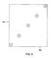
- FIG. 5shows 2 sides ( 501 and 502 ) of the substrate that are close to the sides with pumping channels closed and the 5 measurement locations on a substrate.
- FIG. 6A(Prior Art) illustrates the concept of hollow cathode effect.
- FIGS. 6B-6Gillustrates various designs of hollow cathode cavities.
- FIG. 7Ashows the definition of diameter “D”, the depth “d” and the flaring angle “ ⁇ ” of the bore that extends to the downstream end of a gas passage.
- FIG. 7Bshows the dimensions of a gas passage.
- FIG. 7Cshows the dimensions of a gas passage.
- FIG. 7Dshows the dimensions of a gas passage.
- FIG. 7Eshows the distribution of gas passages across a diffuser plate.
- FIG. 8shows the deposition rate measurement across a 1500 mm by 1800 mm substrate collected from deposition with a diffuser plate with a distribution of gas passages across the diffuser plate as shown in FIG. 7E .
- FIG. 9Ashows the process flow of making a diffuser plate.
- FIG. 9Bshows a bent diffuser plate.
- FIG. 9Cshows a diffuser plate that was previously bent and the side that facing the downstream side was machined to be flat.
- FIG. 9Dshows the distribution of depths of diffuser bores that extends to the downstream ends of gas passages of a diffuser plate used to process 1500 mm by 1850 mm substrates.
- FIG. 9Eshows the measurement of deposition rates across a 1500 mm by 1850 mm substrate.
- FIG. 9Fshows the distribution of depths of diffuser bores that extends to the downstream ends of gas passages of a diffuser plate used to process 1870 mm by 2200 mm substrates.
- FIG. 9Gshows the measurement of deposition rates across an 1870 mm by 2200 mm substrate.
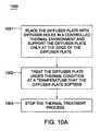
- FIG. 10Ashows the process flow of bending the diffuser plate by a thermal process.
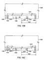
- FIG. 10Bshows the diffuser plate on the supports in the thermal environment that could be used to bend the diffuser plate.
- FIG. 10Cshows the convex diffuser plate on the supports in the thermal environment.
- FIG. 11Ashows the process flow of bending the diffuser plate by a vacuum process.
- FIG. 11Bshows the diffuser plate on the vacuum assembly.
- FIG. 11Cshows the convex diffuser plate on the vacuum assembly.
- FIG. 12Ashows the process flow of creating a diffuser plate with varying diameters and depths of bores that extends to the downstream side of the diffuser plate.
- FIG. 12Bshows the cross section of a diffuser plate with varying diameters and depths of bores that extends to the downstream side of the diffuser plate.
- FIG. 12Cshows a diffuser plate with substantially identical diffuser holes from center to edge of the diffuser plate.
- FIG. 12Dshows the diffuser plate of FIG. 12C after the bottom surface has been machined into a concave shape.
- FIG. 12Eshows the diffuser plate of FIG. 12D after its bottom surface has been pulled substantially flat.
- FIG. 12Fshows a diffuser plate, without any diffuser holes, that has been bent into a concave (bottom surface) shape.
- FIG. 12Gshows the diffuser plate of FIG. 12F with diffuser holes.
- FIG. 12Hshows the diffuser plate of FIG. 12G after its bottom surface has been pulled substantially flat.
- FIG. 12Ishows a diffuser plate with diffuser holes in multiple zones.
- FIG. 12Jshows a diffuser plate with mixed hollow cathode cavity diameters and the inner region hollow cathode cavity volume and/or surface area density is higher than the outer region hollow cathode cavity volume and/or surface area density.
- FIG. 12Kshows a diffuser plate with most of the hollow cathode cavities the same, while there are a few larger hollow cathode cavities near the edge of the diffuser plate.
- FIG. 13shows the downstream side view of a diffuser plate with varying diffuser hole densities.
- the inventiongenerally provides a gas distribution assembly for providing gas delivery within a processing chamber.
- the inventionis illustratively described below in reference to a plasma enhanced chemical vapor deposition system configured to process large area substrates, such as a plasma enhanced chemical vapor deposition (PECVD) system, available from AKT, a division of Applied Materials, Inc., Santa Clara, Calif.
- PECVDplasma enhanced chemical vapor deposition
- AKTa plasma enhanced chemical vapor deposition
- the inventionhas utility in other system configurations such as etch systems, other chemical vapor deposition systems and any other system in which distributing gas within a process chamber is desired, including those systems configured to process round substrates.
- FIG. 1illustrates cross-sectional schematic views of a thin film transistor structure.
- a common TFT structureis the back channel etch (BCE) inverted staggered (or bottom gate) TFT structure shown in FIG. 1 .
- the BCE processis preferred, because the gate dielectric (SiN), and the intrinsic as well as n+ doped amorphous silicon films can be deposited in the same PECVD pump-down run.
- the BCE process shown hereinvolves only 5 patterning masks.
- the substrate 101may comprise a material that is essentially optically transparent in the visible spectrum, such as, for example, glass or clear plastic.
- the substratemay be of varying shapes or dimensions.
- the substrateis a glass substrate with a surface area greater than about 500 mm 2 .
- a gate electrode layer 102is formed on the substrate 101 .
- the gate electrode layer 102comprises an electrically conductive layer that controls the movement of charge carriers within the TFT.
- the gate electrode layer 102may comprise a metal such as, for example, aluminum (Al), tungsten (W), chromium (Cr), tantalum (Ta), or combinations thereof, among others.
- the gate electrode layer 102may be formed using conventional deposition, lithography and etching techniques. Between the substrate 101 and the gate electrode layer 102 , there may be an optional insulating material, for example, such as silicon dioxide (SiO 2 ) or silicon nitride (SiN), which may also be formed using an embodiment of a PECVD system described in this invention.
- the gate electrode layer 102is then lithographically patterned and etched using conventional techniques to define the gate electrode.
- a gate dielectric layer 103is formed on the gate electrode layer 102 .
- the gate dielectric layer 103may be silicon dioxide (SiO 2 ), silicon oxynitride (SiON), or silicon nitride (SiN), deposited using an embodiment of a PECVD system described in this invention.
- the gate dielectric layer 103may be formed to a thickness in the range of about 100 ⁇ to about 6000 ⁇ .
- a bulk semiconductor layer 104is formed on the gate dielectric layer 103 .
- the bulk semiconductor layer 104may comprise polycrystalline silicon (polysilicon) or amorphous silicon ( ⁇ -Si), which could be deposited using an embodiment of a PECVD system described in this invention or other conventional methods known to the art.
- Bulk semiconductor layer 104may be deposited to a thickness in the range of about 100 ⁇ to about 3000 ⁇ .
- a doped semiconductor layer 105is formed on top of the semiconductor layer 104 .
- the doped semiconductor layer 105may comprise n-type (n+) or p-type (p+) doped polycrystalline (polysilicon) or amorphous silicon ( ⁇ -Si), which could be deposited using an embodiment of a PECVD system described in this invention or other conventional methods known to the art. Doped semiconductor layer 105 may be deposited to a thickness within a range of about 100 ⁇ to about 3000 ⁇ . An example of the doped semiconductor layer 105 is n+ doped ⁇ -Si film.
- the bulk semiconductor layer 104 and the doped semiconductor layer 105are lithographically patterned and etched using conventional techniques to define a mesa of these two films over the gate dielectric insulator, which also serves as storage capacitor dielectric.
- the doped semiconductor layer 105directly contacts portions of the bulk semiconductor layer 104 , forming a semiconductor junction.
- a conductive layer 106is then deposited on the exposed surface.
- the conductive layer 106may comprise a metal such as, for example, aluminum (Al), tungsten (W), molybdenum (Mo), chromium (Cr), tantalum (Ta), and combinations thereof, among others.
- the conductive layer 106may be formed using conventional deposition techniques. Both the conductive layer 106 and the doped semiconductor layer 105 may be lithographically patterned to define source and drain contacts of the TFT. Afterwards, a passivation layer 107 may be deposited. Passivation layer 107 conformably coats exposed surfaces.
- the passivation layer 107is generally an insulator and may comprise, for example, silicon dioxide (SiO 2 ) or silicon nitride (SiN).
- the passivation layer 107may be formed using, for example, PECVD or other conventional methods known to the art.
- the passivation layer 107may be deposited to a thickness in the range of about 1000 ⁇ to about 5000 ⁇ .
- the passivation layer 107is then lithographically patterned and etched using conventional techniques to open contact holes in the passivation layer.
- a transparent conductor layer 108is then deposited and patterned to make contacts with the conductive layer 106 .
- the transparent conductor layer 108comprises a material that is essentially optically transparent in the visible spectrum and is electrically conductive.
- Transparent conductor layer 108may comprise, for example, indium tin oxide (ITO) or zinc oxide, among others. Patterning of the transparent conductive layer 108 is accomplished by conventional lithographical and etching techniques.
- the doped or un-doped (intrinsic) amorphous silicon ( ⁇ -Si), silicon dioxide (SiO2), silicon oxynitride (SiON) and silicon nitride (SiN) films used in liquid crystal displays (or flat panels)could all be deposited using an embodiment of a plasma enhanced chemical vapor deposition (PECVD) system described in this invention.
- PECVDplasma enhanced chemical vapor deposition
- the TFT structure described hereis merely used as an example. The current invention applies to manufacturing any devices that are applicable.
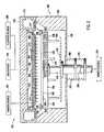
- FIG. 2is a schematic cross-sectional view of one embodiment of a plasma enhanced chemical vapor deposition system 200 , available from AKT, a division of Applied Materials, Inc., Santa Clara, Calif.
- the system 200generally includes a processing chamber 202 coupled to a gas source 204 .
- the processing chamber 202has walls 206 and a bottom 208 that partially define a process volume 212 .
- the process volume 212is typically accessed through a port (not shown) in the walls 206 that facilitate movement of a substrate 240 into and out of the processing chamber 202 .
- the walls 206 and bottom 208are typically fabricated from a unitary block of aluminum or other material compatible with processing.
- the walls 206support a lid assembly 210 that contains a pumping plenum 214 that couples the process volume 212 to an exhaust port (that includes various pumping components, not shown).
- a temperature controlled substrate support assembly 238is centrally disposed within the processing chamber 202 .
- the support assembly 238supports a glass substrate 240 during processing.
- the substrate support assembly 238comprises an aluminum body 224 that encapsulates at least one embedded heater 232 .
- the heater 232such as a resistive element, disposed in the support assembly 238 , is coupled to an optional power source 274 and controllably heats the support assembly 238 and the glass substrate 240 positioned thereon to a predetermined temperature.
- the heater 232maintains the glass substrate 240 at a uniform temperature between about 150 to at least about 460 degrees Celsius, depending on the deposition processing parameters for the material being deposited.
- the support assembly 238has a lower side 226 and an upper side 234 .
- the upper side 234supports the glass substrate 240 .
- the lower side 226has a stem 242 coupled thereto.
- the stem 242couples the support assembly 238 to a lift system (not shown) that moves the support assembly 238 between an elevated processing position (as shown) and a lowered position that facilitates substrate transfer to and from the processing chamber 202 .
- the stem 242additionally provides a conduit for electrical and thermocouple leads between the support assembly 238 and other components of the system 200 .
- a bellows 246is coupled between support assembly 238 (or the stem 242 ) and the bottom 208 of the processing chamber 202 .
- the bellows 246provides a vacuum seal between the chamber volume 212 and the atmosphere outside the processing chamber 202 while facilitating vertical movement of the support assembly 238 .
- the support assembly 238generally is grounded such that RF power supplied by a power source 222 to a gas distribution plate assembly 218 positioned between the lid assembly 210 and substrate support assembly 238 (or other electrode positioned within or near the lid assembly of the chamber) may excite gases present in the process volume 212 between the support assembly 238 and the distribution plate assembly 218 .
- the RF power from the power source 222is generally selected commensurate with the size of the substrate to drive the chemical vapor deposition process.
- the support assembly 238additionally supports a circumscribing shadow frame 248 .
- the shadow frame 248prevents deposition at the edge of the glass substrate 240 and support assembly 238 so that the substrate does not stick to the support assembly 238 .
- the support assembly 238has a plurality of holes 228 disposed therethrough that accept a plurality of lift pins 250 .
- the lift pins 250are typically comprised of ceramic or anodized aluminum.
- the lift pins 250may be actuated relative to the support assembly 238 by an optional lift plate 254 to project from the support surface 230 , thereby placing the substrate in a spaced-apart relation to the support assembly 238 .
- the lid assembly 210provides an upper boundary to the process volume 212 .
- the lid assembly 210typically can be removed or opened to service the processing chamber 202 .
- the lid assembly 210is fabricated from aluminum (Al).
- the lid assembly 210includes a pumping plenum 214 formed therein coupled to an external pumping system (not shown). The pumping plenum 214 is utilized to channel gases and processing by-products uniformly from the process volume 212 and out of the processing chamber 202 .
- the lid assembly 210typically includes an entry port 280 through which process gases provided by the gas source 204 are introduced into the processing chamber 202 .
- the entry port 280is also coupled to a cleaning source 282 .
- the cleaning source 282typically provides a cleaning agent, such as dissociated fluorine, that is introduced into the processing chamber 202 to remove deposition by-products and films from processing chamber hardware, including the gas distribution plate assembly 218 .
- the gas distribution plate assembly 218is coupled to an interior side 220 of the lid assembly 210 .
- the gas distribution plate assembly 218is typically configured to substantially follow the profile of the glass substrate 240 , for example, polygonal for large area flat panel substrates and circular for wafers.
- the gas distribution plate assembly 218includes a perforated area 216 through which process and other gases supplied from the gas source 204 are delivered to the process volume 212 .
- the perforated area 216 of the gas distribution plate assembly 218is configured to provide uniform distribution of gases passing through the gas distribution plate assembly 218 into the processing chamber 202 .
- Gas distribution platesthat may be adapted to benefit from the invention are described in commonly assigned U.S.
- the gas distribution plate assembly 218typically includes a diffuser plate (or distribution plate) 258 suspended from a hanger plate 260 .
- the diffuser plate 258 and hanger plate 260may alternatively comprise a single unitary member.
- a plurality of gas passages 262are formed through the diffuser plate 258 to allow a predetermined distribution of gas passing through the gas distribution plate assembly 218 and into the process volume 212 .
- the hanger plate 260maintains the diffuser plate 258 and the interior surface 220 of the lid assembly 210 in a spaced-apart relation, thus defining a plenum 264 therebetween.
- the plenum 264allows gases flowing through the lid assembly 210 to uniformly distribute across the width of the diffuser plate 258 so that gas is provided uniformly above the center perforated area 216 and flows with a uniform distribution through the gas passages 262 .
- the diffuser plate 258is typically fabricated from stainless steel, aluminum (Al), anodized aluminum, nickel (Ni) or other RF conductive material.
- the diffuser plate 258could be cast, brazed, forged, hot iso-statically pressed or sintered.
- the diffuser plate 258is configured with a thickness that maintains sufficient flatness across the aperture 266 as not to adversely affect substrate processing.
- the thickness of the diffuser plate 258is between about 0.8 inch to about 2.0 inches.
- the diffuser plate 258could be circular for semiconductor wafer manufacturing or polygonal, such as rectangular, for flat panel display manufacturing.
- FIG. 3is a partial sectional view of an exemplary diffuser plate 258 that is described in commonly assigned U.S. patent application Ser. No. 10/417,592, titled “Gas Distribution Plate Assembly for Large Area Plasma Enhanced Chemical Vapor Deposition”, filed on Apr. 16, 2003.
- the diffuser plate 258includes a first or upstream side 302 facing the lid assembly 210 and an opposing second or downstream side 304 that faces the support assembly 238 .
- Each gas passage 262is defined by a first bore 310 coupled by an orifice hole 314 to a second bore 312 that combine to form a fluid path through the gas distribution plate 258 .
- the first bore 310extends a first depth 330 from the upstream side 302 of the gas distribution plate 258 to a bottom 318 .
- the bottom 318 of the first bore 310may be tapered, beveled, chamfered or rounded to minimize the flow restriction as gases flow from the first bore into the orifice hole 314 .
- the first bore 310generally has a diameter of about 0.093 to about 0.218 inches, and in one embodiment is about 0.156 inches.
- the second bore 312is formed in the diffuser plate 258 and extends from the downstream side (or end) 304 to a depth 332 of about 0.10 inch to about 2.0 inches.
- the depth 332is between about 0.1 inch to about 1.0 inch.
- the diameter 336 of the second bore 312is generally about 0.1 inch to about 1.0 inch and may be flared at an angle 316 of about 10 degrees to about 50 degrees.
- the diameter 336is between about 0.1 inch to about 0.5 inch and the flaring angle 316 is between 20 degrees to about 40 degrees.
- the surface of the second bore 312is between about 0.05 inch 2 to about 10 inch 2 and preferably between about 0.05 inch 2 to about 5 inch 2 .
- the diameter of second bore 312refers to the diameter intersecting the downstream surface 304 .
- An example of diffuser plate, used to process 1500 mm by 1850 mm substrates,has second bores 312 at a diameter of 0.250 inch and at a flare angle 316 of about 22 degrees.
- the distances 380 between rims 382 of adjacent second bores 312are between about 0 inch to about 0.6 inch, preferably between about 0 inch to about 0.4 inch.
- the diameter of the first bore 310is usually, but not limited to, being at least equal to or smaller than the diameter of the second bore 312 .
- a bottom 320 of the second bore 312may be tapered, beveled, chamfered or rounded to minimize the pressure loss of gases flowing out from the orifice hole 314 and into the second bore 312 .
- the proximity of the orifice hole 314 to the downstream side 304serves to minimize the exposed surface area of the second bore 312 and the downstream side 304 that face the substrate, the downstream area of the diffuser plate 258 exposed to fluorine provided during chamber cleaning is reduced, thereby reducing the occurrence of fluorine contamination of deposited films.
- the orifice hole 314generally couples the bottom 318 of the first hole 310 and the bottom 320 of the second bore 312 .
- the orifice hole 314generally has a diameter of about 0.01 inch to about 0.3 inch, preferably about 0.01 inch to about 0.1 inch, and typically has a length 334 of about 0.02 inch to about 1.0 inch, preferably about 0.02 inch to about 0.5 inch.
- the length 334 and diameter (or other geometric attribute) of the orifice hole 314is the primary source of back pressure in the plenum 264 which promotes even distribution of gas across the upstream side 302 of the gas distribution plate 258 .
- the orifice hole 314is typically configured uniformly among the plurality of gas passages 262 ; however, the restriction through the orifice hole 314 may be configured differently among the gas passages 262 to promote more gas flow through one area of the gas distribution plate 258 relative to another area.
- the orifice hole 314may have a larger diameter and/or a shorter length 334 in those gas passages 262 , of the gas distribution plate 258 , closer to the wall 206 of the processing chamber 202 so that more gas flows through the edges of the perforated area 216 to increase the deposition rate at the perimeter of the glass substrate.
- the thickness of the diffuser plateis between about 0.8 inch to about 3.0 inches, preferably between about 0.8 inch to about 2.0 inch.
- film thickness and property uniformity for large area plasma-enhanced chemical vapor depositionbecomes more problematic.
- noticeable uniformity problemsinclude higher deposition rates and more compressive films in the central area of large substrates for some high deposition rate silicon nitride films.
- the thickness uniformity across the substrateappears “dome shaped” with film in center region thicker than the edge region. The less compressive film in the edge region has higher Si—H content.
- the manufacturing requirements for TFT-LCDinclude low Si—H content, for example ⁇ 15 atomic %, high deposition rate, for example >1500 ⁇ /min, and low thickness non-uniformity, for example ⁇ 15%, across the substrate.
- the Si—H contentis calculated from FTIR (Fourier Transform Infra-Red) measurement.
- FTIRFastier Transform Infra-Red
- the larger substrateshave worse “dome shape” uniformity issue. The problem could not be eliminated by process recipe modification to meet all requirements. Therefore, the issue needs to be addressed by modifying the gas and/or plasma distribution.
- FIG. 4AThe process of depositing a thin film in a process chamber is shown in FIG. 4A .
- the processstarts at step 401 by placing a substrate in a process chamber with a diffuser plate.
- flow process gas(es)through a diffuser plate toward a substrate supported on a substrate support.
- FIG. 4Bshows a thickness profile of a silicon nitride film across a glass substrate.
- the size of the substrateis 1500 mm by 1800 mm.
- the diffuser platehas diffuser holes with design shown in FIG. 3 .
- the diameter of the first bore 310is 0.156 inch.
- the length 330 of the first bore 310is 1.049 inch.
- the diameter 336 of the second bore 312is 0.250 inch.
- the flaring angle 316 of the second bore 312is 22 degree.
- the length 332 of the second bore 312is 0.243 inch.
- the diameter of the orifice hole 314is 0.016 inch and the length 334 of the orifice hole 314 is 0.046 inch.
- the SiN filmis deposited using 2800 sccm SiH 4 , 9600 sccm NH 3 and 28000 sccm N 2 , under 1.5 Torr, and 15000 watts source power.
- the spacing between the diffuser plate and the support assemblyis 1.05 inch.
- the process temperatureis maintained at about 355 ° C.
- the deposition rateis averaged to be 2444 ⁇ /min and the thickness uniformity (with 15 mm edge exclusion) is 25.1%, which is higher than the manufacturing specification ( ⁇ 15%).
- the thickness profileshows a center thick profile, or “dome shape” profile.
- Table 1shows the film properties measured from wafers placed on the glass substrate for the above film. TABLE 1 Measurement of thickness and film properties on a substrate deposited with SiN film. Measure- Stress ment Thickness (E9 Si-H WER location ( ⁇ ) RI Dynes/cm 2 ) (atomic %) ( ⁇ /min ) Edge I 5562 1.92 ⁇ 0.7 12.5 664 Center 8544 1.90 ⁇ 6.7 4.2 456 Edge II 6434 1.91 ⁇ 1.2 10.8 665
- Edge I and Edge IIrepresent two extreme ends of the substrate with width at 1800 mm.
- the refractive index (RI), film stress, Si—H concentration data and wet etch rate (WER) datashow a more compressive film near the center region in comparison to the edge region.
- the Si—H concentrations at the substrate edgesare approaching the manufacturing limit of 15%.
- Wet etch rateis measured by immersing the samples in a BOE (buffered oxide etch) 6:1 solution.
- thermo-resistant tapeis used to block of the pumping channels 214 (shown in FIG. 2 ) near side 501 and side 502 of substrate in a PECVD process chamber.
- the pumping channels 214 near the other two sidesare left open. Due to this, an asymmetric gas pumping situation was created.
- thermo-resistant tape near two edges of the substrateshould worsen the uniformity issue and cause worse uniformity across the substrate.
- the diffuser plate used herehas the same design and dimensions as the one used for FIG. 4B and Table 1 .
- the SiN films in Table 2are deposited using 3300 sccm SiH 4 , 28000 sccm NH 3 and 18000 sccm N 2 , under 1.3 Torr, and 11000 watts source power.
- the spacing between the diffuser plate and the support assemblyis 0.6 inch.
- the process temperatureis maintained at about 355° C.
- Film thickness and propertiesare measured on location 1 , 2 , 3 , 4 and 5 (as shown in FIG. 5 ) on the substrates.
- the SiH content shownis Table 2 is measured in atomic %. TABLE 2 SiN thickness and film properties comparison between deposition with all pumping channels open and with 2 pumping channels closed.
- a possible cause for the center to edge non-uniformityis plasma non-uniformity.
- Deposition of films by PECVDdepends substantially on the source of the active plasma. Dense chemically reactive plasma can be generated due to hollow cathode effect.
- the driving force in the RF generation of a hollow cathode dischargeis the frequency modulated d.c. voltage Vs (the self-bias voltage) across the space charge sheath at the RF electrode.
- Vsthe self-bias voltage
- a RF hollow cathode and oscillation movement of electrons between repelling electric fields, Es, of the opposite sheathsare shown schematically in FIG. 6A .
- An electron emitted from the cathode wallwhich could be the walls of the reactive gas passages that are close to the process volume 212 , is accelerated by the electric field Es across the wall sheath “ ⁇ ”.
- the electronoscillates across the inner space between walls of the electrode owing to the repelling fields of the opposite wall sheaths.
- the electronloses energy by collisions with the gas and creates more ions.
- the created ionscan be accelerated to the cathode walls thereby enhancing emissions of secondary electrons, which could create additional ions.
- the cavities between the cathode wallsenhance the electron emission and ionization of the gas. Flared-cone shaped cathode walls, with gas inlet diameter smaller than the gas outlet diameter, are more efficient in ionizing the gas than cylindrical walls.
- the potential Ezis created due to difference in ionization efficiency between the gas inlet and gas outlet.
- the gas ionizationcould be modified to control the film thickness and property uniformity.
- An example of the walls of the hollow cathode cavities that are close to the process volume 212is the second bore 312 of FIG. 3 .
- the hollow cathode effectmainly occurs in the flared cone 312 that faces the process volume 212 .
- the FIG. 3 designis merely used as an example.
- the inventioncan be applied to other types of hollow cathode cavity designs.
- Other examples of hollow cathode cavity designinclude, but not limited to, the designs shown in FIGS. 6B-6G .
- the volume of second bore (or hollow cathode cavity) 312can be changed by varying the diameter “D” (or diameter 336 in FIG. 3 ), the depth “d” (or length 332 in FIG. 3 ) and the flaring angle “ ⁇ ” (or flaring angle 316 of FIG. 3 ), as shown in FIG. 7A .
- Changing the diameter, depth and/or the flaring anglewould also change the surface area of the bore 312 . Since the center of substrate has higher deposition rate and is more compressive, higher plasma density is likely the cause.
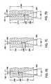
- FIGS. 7B, 7C and 7 Dshow 3 diffuser passage (or diffuser hole) designs that are arranged on a diffuser plate shown in FIG. 7E .
- FIGS. 7B, 7C and 7 D designshave the same cone (or bore) diameter, but the cone (or bore) depth and total cone (bore) surface areas are largest for FIG. 7B design and smallest for FIG. 7D design.
- the cone flaring angleshave been changed to match the final cone diameter.
- the cone depth for FIG. 7Bis 0.7 inch.
- the cone depth for FIG. 7Cis 0.5 inch and the cone depth for FIG. 7D is 0.325 inch.
- the smallest rectangle 710 in FIG. 7Eis 500 mm by 600 mm and the diffuser holes have cone depth 0.325 inch, cone diameter 0.302 inch and flare angel 45° FIG. 7D ).
- the medium rectangle in FIG. 7Eis 1000 mm by 1200 mm.
- the diffuser holes in the area 720 between the medium rectangle and the smallest rectanglehave cone depth 0.5 inch, cone diameter 0.302 inch and flare angle 30° (See FIG. 7C ).
- the largest rectangle in Figureis 1500 mm by 1800 mm.
- the diffuser holes in the area 730 between the largest rectangle and the medium rectanglehave cone depth 0.7 inch, cone diameter 0.302 inch and flare angle 22° (See FIG. 7B )
- the orifice holes diametersare all 0.03 inch and holes depths are all 0.2 inch for FIGS. 7B, 7C and 7 D.
- the thickness of the three diffuser platesare all 1.44 inch.
- the diameters for first bore 310 of FIG. 7B, 7C and 7 Dare all 0.156 inch and the depth are 0.54 inch ( FIG. 7B ), 0.74 inch ( FIG. 7C ) and 0.915 inch ( FIG. 7C ) respectively.
- FIG. 8shows the deposition rate across the substrate.
- Region Icorrelates to the area under “0.325 inch depth” cones, while regions II and III correlates to “0.5 inch depth” (region II) and “0.7 inch depth” (region II) respectively.
- Table 3shows the measurement of film thickness and properties across the substrate.
- the SiN film in Table 3is deposited using 3300 sccm SiH 4 , 28000 sccm NH 3 and 18000 sccm N 2 , under 1.3 Torr, and 11000 watts source power.
- the spacing between the diffuser plate and the support assemblyis 0.6 inch.
- the process temperatureis maintained at about 355° C.
- the locations 1 , 2 , 3 , 4 and 5are the same locations indicated in FIG. 5 .
- the resultsshow that reducing the cone depth and cone surface area reduces the deposition rate.
- the resultsalso show that reducing the volume and/or surface area of hollow cathode cavity reduces the deposition rate.
- the reduction of the plasma deposition ratereflects a reduction in plasma ionization rate. Since the change of cone depth and total cone surface area from region I to region II to region III is not smooth, the deposition rates across the substrate shows three regions. Regions I, II and III on the substrate match the diffuser holes regions 710 , 720 and 730 . This indicates that changing the hollow cathode cavity design can change the plasma ionization rate and also the importance of making the changes smooth and gradual.
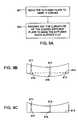
- FIG. 9Ashows the process flow of this concept. The process starts by bending the diffuser plate to make it convex at step 901 , followed by machining out the curvature of the convex diffuser plate to make the diffuser plate surface flat at step 902 .
- FIG. 9Ashows the process flow of this concept. The process starts by bending the diffuser plate to make it convex at step 901 , followed by machining out the curvature of the convex diffuser plate to make the diffuser plate surface flat at step 902 .
- FIG. 9Bshows a schematic drawing of a convex diffuser plate with an exemplary diffuser hole (or gas passage) 911 at the edge (and outer region) and an exemplary diffuser hole 912 in the center (and inner region) as diffuser holes.
- the diffuser holes 911 and 912are identical before the bending process and are simplified drawings of diffuser holes as shown in FIGS. 3 and 7 A.
- the inventioncan be used for any diffuser holes designs.
- the design in FIG. 3is merely used for example.
- Diffuser plate downstream surface 304faces the process volume 212 .
- the gradual changing distance between the 913 surface and the flat 914 surfaceshows the curvature.
- FIG. 9Cshows the schematic drawing of a diffuser plate after the curvature has been machined out.
- the surface facing the process volume 212is machined to 914 (a flat surface), leaving center cone 918 significantly shorter than the edge cone 917 . Since the change of the cone size (volume and/or surface area) is created by bending the diffuser plate followed by machining out the curvature, the change of the cone size (volume and/or surface area) from center to edge is gradual.
- the center cone 918would have diameter “D” and depth “d” smaller than the edge cone 917 .
- the definition of cone diameter “D” and cone depth “d”can be found in the description of FIG. 7A .
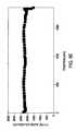
- FIG. 9Dshows the depth “d” of the bores 312 (or cone) that extend to the downstream side of an exemplary diffuser plate, which is used to process 1500 mm by 1850 mm substrates.
- the diffuser platehas diffuser holes with design shown in FIG. 7A .
- the diameter of the first bore 310is 0.156 inch.
- the length 330 of the first bore 310is 1.049 inch.
- the diameter 336 of the second bore 312is 0.250 inch.
- the flaring angle 316 of the second bore 312is 22degree.
- the length 332 of the second bore 312is 0.243 inch.
- the diameter of the orifice hole 314is 0.016 inch and the length 334 of the orifice hole 314 is 0.046 inch.
- 9Dshows a gradual increasing of bore depth 332 (or “d” in FIG. 7A ) from center of the diffuser plate to the edge of the diffuser plate. Due to the bending and machining processes, the diameter 336 (or “D” in FIG. 7A ) of the bore 312 also gradually increases from center of the diffuser plate to the edge of the diffuser plate.
- FIG. 9Eshows the thickness distribution across a substrate deposited with SiN film under a diffuser plate with a design described in FIGS. 9B, 9C and 9 D.
- the size of substrateis 1500 mm by 1850 mm, which is only slightly larger than the size of substrate (1500 mm by 1800 mm) in FIG. 4B and Table 1 .
- the diffuser plate sizesscale with the substrate sizes.
- the diffuser plate used to process 1500 mm by 1850 mm substratesis about 1530 mm by 1860 mm, which is slightly larger than the diffuser plate used to process 1500 mm by 1800 mm substrates (diffuser plate about 1530 mm by 1829 mm).
- the thickness uniformityis improved to 5.0%, which is much smaller than 25.1% for film in FIG. 4B .
- Table 4shows the film property distribution across the substrate.
- the diffuser platehas diffuser holes with design shown in FIG. 7A .
- the diameter of the first bore 310is 0.156 inch.
- the length 330 of the first bore 310is 1.049 inch.
- the diameter 336 of the second bore 312is 0.250 inch.
- the flaring angle 316 of the second bore 312is 22 degree.
- the length 332 of the second bore 312is 0.243 inch.
- the diameter of the orifice hole 314is 0.016 inch and the length 334 of the orifice hole 314 is 0.046 inch.
- 9E and Table 4are deposited using 2800 sccm SiH 4 , 9600 sccm NH 3 and 28000 sccm N 2 , under 1.5 Torr, and 15000 watts source power.
- the spacing between the diffuser plate and the support assemblyis 1.05 inch.
- the process temperatureis maintained at about 355° C.
- Edge I and Edge IIrepresent two extreme ends of the substrate, as described in Table 1 measurement.
- the film thickness and property data in Table 4show much smaller center to edge variation compared to the data in Table 1. TABLE 4 SiN film thickness and property measurement using a diffuser plate with gradually varied bore depths and diameters from center to edge for a 1500 mm by 1850 mm substrate.
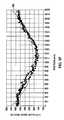
- FIG. 9Fshows the depth “d” measurement of the bores 312 across an exemplary diffuser plate, which is used to process 1870 mm by 2200 mm substrates
- Curve 960shows an example of an ideal bore depth distribution the diffuser plate.
- the measurement of depths of the bores in FIG. 9Fshows a gradual increasing of bore depth from center of the diffuser plate to the edge of the diffuser plate.
- the downstream bore diameterwould also gradually increase from center of the diffuser plate to the edge of the diffuser plate.
- FIG. 9Gshows the thickness distribution across a substrate deposited with SiN film under a diffuser plate with a design similar to the one described in FIGS. 9B, 9C and 9 F.
- the size of the substrateis 1870 mm by 2200 mm.
- Table 5shows the film property distribution across the substrate.
- the diffuser platehas diffuser holes with design shown in FIG. 7A .
- the diameter of the first bore 310is 0.156 inch.
- the length 330 of the first bore 310is 0.915 inch.
- the diameter 336 of the second bore 312is 0.302 inch.
- the flaring angle 316 of the second bore 312is 22 degree.
- the length 332 of the second bore 312is 0.377 inch.
- the diameter of the orifice hole 314is 0.018 inch and the length 334 of the orifice hole 314 is 0.046 inch.
- the SiN films in Table 5are deposited using 5550 sccm SiH 4 , 24700 sccm NH 3 and 61700 sccm N 2 , under 1.5 Torr, and 19000 watts source power.
- the spacing between the diffuser plate and the support assemblyis 1.0 inch.
- the process temperatureis maintained at about 350° C.
- Edge I and Edge IIrepresent two extreme ends of the substrate, as described in Table 1 measurement.
- the film thickness and property data in Table 5show much smaller center to edge variation compared to the data in Table 1.
- the thickness uniformityis 9.9%, which is much better than 25.1% for film in FIG. 4B .
- the data shown in FIG. 4B and Table 1are film thickness and property data on smaller substrate (1500 mm by 1800 mm), compared to the substrate (1870 mm by 2200 mm) for data in FIG. 9G and Table 5. Thickness and property uniformities are expected to be worse for larger substrate.
- the uniformity of 9.9% and the improved film property data in Table 5 by the new designshow that the new design, with gradual increasing diameters and depths of diffuser bores extended to the downstream side of the diffuser plate, greatly improves the plasma uniformity and process uniformity.
- TABLE 5SiN film thickness and property measurement using a diffuser plate with gradually varied bore depths and diameters from center to edge for an 1870 mm by 2200 mm substrate.
- the exemplary diffuser plate described hereis rectangular, the invention applies to diffuser plate of other shapes and sizes.
- the convex downstream surfacedoes not have to be machined to be completely flat across the entire surface. As long as the diameters and depths of the bores are increased gradually from center to edge of the diffuser plate, the edge of the diffuser plate could be left un-flattened.
- FIG. 10Ashows the process flow 1000 of such thermal treatment.
- step 1001place the diffuser plate, which already has diffuser holes in it, in an environment 1005 or chamber that could be thermally controlled and place the diffuser plate 1010 on a support 1020 that only support the edge of the diffuser plate (See FIG. 10B ).
- the diffuser plate facing downis the downstream surface 304 of the diffuser plate.
- One embodimentis to keep the thermal environment at a constant treatment temperature (iso-thermal), once the constant treatment temperature has been reached.
- optional diffuser support 1030could be placed under diffuser plate 1010 at support height 1035 lower than the support height 1025 of support 1020 and at a support distance 1037 shorter than the support distance 1027 of support 1020 .
- the optional support 1030could help determine the diffuser curvature and could be made of elastic materials that could withstand temperature greater than 400° C. (the same temperature as the thermal conditioning temperature) and would not damage the diffuser plate surface.
- FIG. 10Cshows that the curved diffuser plate 1010 resting on the diffuser plate supports 1020 and 1030 after the bending process.
- FIG. 11Ashows the process flow 1100 of such bending by vacuum process.
- step 1101place the diffuser plate, which already has diffuser holes in it and the downstream side 304 facing down, on a vacuum assembly 1105 and seal the upstream end 302 of the diffuser plate with a cover.
- the material used to cover (or seal) the upstream end of the diffuser platemust be strong enough to keep its integrity under vacuum.
- the vacuum assemblyonly supports the diffuser plate at the edge (See FIG. 11B ) by diffuser plate holder 1120 .
- the vacuum assembly 1105is configured to have a pump channel 1150 to pull vacuum in the volume 1115 between the diffuser plate and the vacuum assembly 1105 when the upstream end of the diffuser plate is covered.
- the pumping channel 1150 in FIGS. 11B and 11Care merely used to demonstrate the concept. There could be more than one pumping channels placed at different locations in the vacuum assembly 1105 .
- pull vacuum in the volume 1115 between the diffuser plate and the diffuser plate holderWhen the curvature of the diffuser plate has reached the desired curvature, stop the vacuuming process at step 1103 and restore the pressure of the volume 1115 between the diffuser plate and the vacuum assembly to be equal to the surrounding environment 1140 to allow the diffuser plate to be removed from the vacuum assembly 1105 .
- optional diffuser support 1130could be placed under diffuser plate 1110 at support height 1135 lower than the support height 1125 of the diffuser plate support 1120 and at a support distance 1137 shorter than the support distance 1127 of support 1120 .
- the optional supportcould help determine the diffuser curvature and could be made of materials, such as rubber, that would not damage the diffuser plate surface.
- FIG. 11Cshows that the curved diffuser plate 1110 resting on the diffuser plate supports 1120 and 1130 after the bending process.
- FIG. 12Ashows the process flow of such a process 1200 .
- the process 1200starts at step 1230 by creating bores that extend to the downstream side of a diffuser plate with gradually increasing bore depths and/or bore diameters from center to edge of the diffuser plate.
- the flaring anglecan also be varied from center to edge of the diffuser plate.
- step 1240the process is completed by creating the remaining portions of the gas passages of the diffuser plate.
- the downstream conescan be created by using drill tools. If drill tools with the same flaring angle are used across the diffuser plate, the cone flaring angles would stay constant and cone depth and cone diameter are varied. The cone diameter would be determined by the flaring angle and cone depth. The important thing is to vary the cone depth smoothly and gradually to ensure smooth deposition thickness and film property change across the substrate.
- FIG. 12Bshows an example of varying cone depths and cone diameters. Diffuser hole 1201 is near the center of the diffuser plate and has the smallest cone depth 1211 and cone diameter 1221 .
- Diffuser hole 1202is between the center and edge of the diffuser plate and has the medium cone depth 1212 and cone diameter 1222 .
- Diffuser hole 1203is near the edge of the diffuser plate and has the largest cone depth 1213 and cone diameter 1223 .
- the cone flaring angle of all diffuser holesare the same for the design in FIG. 12B . However, it is possible to optimize deposition uniformity by varying the cone design across the diffuser plate by varying both the cone diameters, cone depths and flaring angles. Changing the cone depth, cone diameter and cone flaring angle affects the total cone surface area, which also affects the hollow cathode effect. Smaller cone surface area lowers the plasma ionization efficiency.
- FIG. 12CYet another way to change the downstream bore ( 312 in FIG. 3 ) depth (“d”), and bore diameter (“D”) is by drilling identical diffuser holes across the diffuser plate (see FIG. 12C ).
- the gas diffuser hole 1251 at the edge (at outer region) of the diffuser plateis identical to the gas diffuser hole 1252 at the center (at inner region) of the diffuser plate.
- the downstream bore 1255is also identical to downstream bore 1256 .
- the downstream surface 1254 of gas diffuser plateis initially flat. Afterwards, machine downstream side of the diffuser plate to make a concave shape with center thinner than the edge.
- the machiningcan be achieved by computer numerically controlled machining or other types of controlled machining to make the machining process repeatable.
- the downstream bore 1258 at the center (an inner region) of the diffuser platehas smaller diameter (“D”) and smaller length (“d”) than the downstream bore 1257 at the edge (an outer region) of the diffuser plate.
- the diffuser platecan be left the way it is as in FIG. 12D , or downstream surface 1259 can be pulled flat as shown in FIG. 12E , or to other curvatures (not shown), to be used in a process chamber to achieve desired film results.
- downstream bore ( 312 in FIG. 3 ) depth (“d”), and bore diameter (“D”)is by bending the diffuser plate without any diffuser hole into concave shape (See FIG. 12F ).
- the downstream surfaceis surface 1269 .
- downstream bore 1268 at the center of the diffuser plateis drilled to the same depth from the fictitious surface 1264 as the downstream bore 1267 , the diameter and length of the downstream bore 1268 are smaller than the diameter and length of the downstream bore 1267 .
- the rest of the diffuser holeswhich include orifice holes 1265 , upstream bores 1263 , and connecting bottoms, are machined to complete the diffuser holes. All orifice holes and upstream bores should have identical diameters, although it is not necessary. The diameters and lengths of the orifice holes should be kept the same across the diffuser plate (as shown in FIG. 12G ). The orifice holes controls the back pressure. By keeping the diameters and the lengths of the orifice holes the same across the diffuser plate, the back pressure, which affects the gas flow, can be kept the same across the diffuser plate.
- the diffuser platecan be left the way it is as in FIG. 12G , or downstream surface 1269 can be pulled flat as shown in FIG. 12H , or to other curvatures (not shown), to be used in a process chamber to achieve desired film results.
- FIG. 12Ishows a schematic plot of bottom view (looking down at the downstream side) of a diffuser plate.
- the diffuser plateis divided into N concentric zones.
- Concentric zonesare defined as areas between an inner and an outer boundaries, which both have the same geometric shapes as the overall shape of the diffuser plate. Within each zone, the diffuser holes are identical. From zone 1 to zone N, the hollow cathode cavity gradually increase in size (volume and/or surface area). The increase can be accomplished by increase of hollow cathode cavity diameter, length, flaring angle, or a combination of these parameters.
- the increase of diameters and/or lengths of the hollow cathode cavities from center to edge of the diffuser platealso do not have to apply to all diffuser holes, as long as there is an overall increase in the size (volume and/or surface area) of hollow cathode cavities per downstream diffuser plate surface area of the hollow cathode cavities.
- some diffuser holescould be kept the same throughout the diffuser plate, while the rest of the diffuser holes have a gradual increase in the sizes (volumes and/or surface areas) of the hollow cathode cavities.
- the diffuser holeshave a gradual increase in sizes (volumes and/or surface areas) of the hollow cathode cavities, while there are some small hollow cathode cavities at the edge of the diffuser plate, as shown in FIG. 12J .
- most of the hollow cathode cavitiesare uniform across the diffuser plate, while there are a few larger hollow cathode cavities towards the edge of the diffuser plate, as shown in FIG. 12K .
- hollow cathode cavity volume densityas the volumes of the hollow cathode cavities per downstream diffuser plate surface area of the hollow cathode cavities.
- hollow cathode cavity surface area density of the hollow cathode cavityas the total surface areas of the hollow cathode cavities per downstream diffuser plate surface area of the hollow cathode cavities.
- the density of diffuser holesis calculated by dividing the total surface of holes of bores 312 intersecting the downstream side 304 by the total surface of downstream side 304 of the diffuser plate in the measured region.
- the density of diffuser holescan be varied from about 10% to about 100%, and preferably varied from 30% to about 100%.
- the diffuser holes densityshould be lowered in the inner region, compared to the outer region, to reduce the plasma density in the inner region.
- the density changes from the inner region to the outer regionshould be gradual and smooth to ensure uniform and smooth deposition and film property profiles.
- FIG. 13shows the gradual change of diffuser holes density from low in the center (region A) to high at the edge (region B).
- the lower density of diffuser holes in the center regionwould reduce the plasma density in the center region and reduce the “dome shape” problem.
- the arrangement of the diffuser holes in FIG. 13is merely used to demonstrate the increasing diffuser holes densities from center to edge.
- the inventionapplies to any diffuser holes arrangement and patterns.
- the density change conceptcan also be combined with the diffuser hole design change to improve center to edge uniformity.
- the spacing of hollow cathode cavities at the down stream endcould exceed 0.6 inch.
- the inventive concept of gradual increase of hollow cathode cavity size (volume and/or surface area) from the center of the diffuser plate to the edge of the diffuser platecan be accomplished by a combination of the one of the hollow cathode cavity size (volume and/or surface area) and shape variation, with or without the diffuser hole density variation, with one of the diffuser plate bending method, and with one of the hollow cathode cavity machining methods applicable.
- the concept of increasing density of diffuser holes from the center to the edge of the diffuser platecan be used increasing the diameter of the hollow cathode cavity (or downstream bore) from the center to the edge of the diffuser plate.
- the diffuser platecould be kept flat and the diffuser holes are drilled by CNC method.
- the combinationis numerous. Therefore, the concept is very capable of meeting the film thickness and property uniformity requirements.
- the various embodiments of the inventionare mainly described to increase the diameters and lengths of the hollow cathode cavities from center of the diffuser plate to the edge of the diffuser plate to improve the plasma uniformity across the substrate.
- the diameter and the lengths of the hollow cathode cavitiesmight decrease from the center of the diffuser plate to the edge of the diffuser plate.
- the power sourcemight be lower near the center of the substrate and the hollow cathode cavities need to be larger to compensate for the lower power source.
- the concept of the inventiontherefore, applies to decreasing the sizes (volumes and/or areas) hollow cathode cavities from the center of the diffuser plate to the edge of the diffuser plate.
- the concept of the inventionapplies to any design of gas diffuser holes, which includes any design of hollow cathode cavity, and any shapes/sizes of gas diffuser plates.
- the concept of the inventionapplies to a diffuser plate that utilizes multiple designs of gas diffuser holes, which include multiple designs of hollow cathode cavities.
- the concept of the inventionapplies to diffuser plate of any curvatures and diffuser plate made of any materials, for example, aluminum (Al), tungsten (W), chromium (Cr), tantalum (Ta), or combinations thereof, among others, and by any methods, for example, cast, brazed, forged, hot iso-statically pressed or sintered.
- the concept of the inventionalso applies to diffuser plate made of multiple layers of materials that are pressed or glued together.
- the concept of the inventioncan be used in a chamber that could be in a cluster system, a stand-alone system, an in-line system, or any systems that are applicable.
Landscapes
- Chemical & Material Sciences (AREA)
- Engineering & Computer Science (AREA)
- Physics & Mathematics (AREA)
- Plasma & Fusion (AREA)
- Analytical Chemistry (AREA)
- Mechanical Engineering (AREA)
- Chemical Kinetics & Catalysis (AREA)
- Materials Engineering (AREA)
- General Chemical & Material Sciences (AREA)
- Metallurgy (AREA)
- Organic Chemistry (AREA)
- Inorganic Chemistry (AREA)
- Chemical Vapour Deposition (AREA)
- Drying Of Semiconductors (AREA)
- Formation Of Insulating Films (AREA)
- Physical Or Chemical Processes And Apparatus (AREA)
- Plasma Technology (AREA)
Abstract
Description
- This application claims benefit of U.S. provisional patent application Ser. No. 60/570,876, filed May 12, 2004, which is herein incorporated by reference.
- 1. Field of the Invention
- Embodiments of the invention generally relate to a gas distribution plate assembly and method for distributing gas in a processing chamber.
- 2. Description of the Background Art
- Liquid crystal displays or flat panels are commonly used for active matrix displays such as computer and television monitors. Plasma enhanced chemical vapor deposition (PECVD) is generally employed to deposit thin films on a substrate such as a transparent substrate for flat panel display or semiconductor wafer. PECVD is generally accomplished by introducing a precursor gas or gas mixture into a vacuum chamber that contains a substrate. The precursor gas or gas mixture is typically directed downwardly through a distribution plate situated near the top of the chamber. The precursor gas or gas mixture in the chamber is energized (e.g., excited) into a plasma by applying radio frequency (RF) power to the chamber from one or more RF sources coupled to the chamber. The excited gas or gas mixture reacts to form a layer of material on a surface of the substrate that is positioned on a temperature controlled substrate support. Volatile by-products produced during the reaction are pumped from the chamber through an exhaust system.
- Flat panels processed by PECVD techniques are typically large, often exceeding 370 mm×470 mm. Large area substrates approaching and exceeding 4 square meters are envisioned in the near future. Gas distribution plates (or gas diffuser plates) utilized to provide uniform process gas flow over flat panels are relatively large in size, particularly as compared to gas distribution plates utilized for 200 mm and 300 mm semiconductor wafer processing.
- As the size of substrates continues to grow in the TFT-LCD industry, film thickness and film property uniformity control for large area plasma-enhanced chemical vapor deposition (PECVD) becomes an issue. TFT is one type of flat panel display. The difference of deposition rate and/or film property, such as film stress, between the center and the edge of the substrate becomes significant.
- Therefore, there is a need for an improved gas distribution plate assembly that improves the uniformities of film deposition thickness and film properties.
- Embodiments of a gas distribution plate for distributing gas in a processing chamber are provided. In one embodiment, a gas distribution plate assembly for a plasma processing chamber comprises a diffuser plate having an upstream side and a downstream side, and inner and outer gas passages passing between the upstream and downstream sides of the diffuser plate and comprising hollow cathode cavities at the downstream side, wherein the hollow cathode cavity volume density of the inner gas passages are less than the hollow cathode cavity volume density of the outer gas passages.
- In another embodiment, a gas distribution plate assembly for a plasma processing chamber comprises a diffuser plate having an upstream side and a downstream side, and inner and outer gas passages passing between the upstream and downstream sides of the diffuser plate and comprising hollow cathode cavities at the downstream side, wherein the hollow cathode cavity surface area density of the inner gas passages are less than the hollow cathode cavity surface area density of the outer gas passages.
- In another embodiment, a gas distribution plate assembly for a plasma processing chamber comprises a diffuser plate having an upstream side and a down stream side, and a plurality of gas passages passing between the upstream and downstream sides of the diffuser plate, wherein the densities of hollow cathode cavities gradually increase from the center to the edge of the diffuser plate.
- In another embodiment, a plasma processing chamber comprises a diffuser plate having an upstream side and a downstream side, inner and outer gas passages passing between the upstream and downstream sides of the diffuser plate and comprising hollow cathode cavities at the downstream side, wherein the hollow cathode cavity volume density of the inner gas passages are less than the hollow cathode cavity volume density of the outer gas passages, and a substrate support adjacent the downstream side of the diffuser plate.
- In another embodiment, a plasma processing chamber comprises a diffuser plate having an upstream side and a downstream side, inner and outer gas passages passing between the upstream and downstream sides of the diffuser plate and comprising hollow cathode cavities at the downstream side, wherein the hollow cathode cavity surface area density of the inner gas passages are less than the hollow cathode cavity surface area density of the outer gas passages, and a substrate support adjacent the downstream side of the diffuser plate.
- In another embodiment, a plasma processing chamber comprises a diffuser plate having an upstream side and a down stream side, a plurality of gas passages passing between the upstream and downstream sides of the diffuser plate, wherein the densities of hollow cathode cavities gradually increase from the center to the edge of the diffuser plate, and a substrate support adjacent the downstream side of the diffuser plate.
- In another embodiment, a gas distribution plate assembly for a plasma processing chamber comprises a diffuser plate having an upstream side and a down stream side and the gas diffuser plate are divided into a number of concentric zones, and a plurality of gas passages passing between the upstream and downstream sides of the diffuser plate, wherein the gas passages in each zones are identical and the density, the volume, or surface area of hollow cathode cavities of gas passages in each zone gradually increase from the center to the edge of the diffuser plate.
- In another embodiment, a method of making a gas diffuser plate for a plasma processing chamber, comprises making a gas diffuser plate to have an upstream side and a down stream side, and a plurality of gas passages passing between the upstream and downstream sides of the diffuser plate, bending the diffuser plate to make it convex smoothly toward downstream side, and machining out the convex surface to flatten the downstream side surface.
- In another embodiment, a method of making a gas diffuser plate for a plasma processing chamber comprises machining a gas diffuser plate to have an upstream side and a down stream side, and a plurality of gas passages passing between the upstream and downstream sides of the diffuser plate, wherein densities, volumes or surface area of hollow cathode cavities of the diffuser plate gradually increase from the center to the edge of the diffuser plate.
- In another embodiment, a method of depositing a thin film on a substrate comprises placing a substrate in a process chamber with a gas diffuser plate having an upstream side and inner and outer gas passages passing between the upstream and downstream sides of the diffuser plate and comprising hollow cathode cavities at the downstream side, wherein either the hollow cathode cavity volume density, or the hollow cathode cavity surface area density, or the hollow cathode cavity density of the inner gas passages are less than the same parameter of the outer gas passages, flowing process gas(es) through a diffuser plate toward a substrate supported on a substrate support, creating a plasma between the diffuser plate and the substrate support, and depositing a thin film on the substrate in the process chamber.
- In another embodiment, a diffuser plate comprises a body having a top surface and a bottom surface, a plurality of gas passages between the top surface the bottom surface, and an outer region and an inner region wherein the body between the top and the bottom of the outer region is thicker than the body between the top and the bottom of the inner region.
- In another embodiment, a method of making a gas diffuser plate for a plasma processing chamber comprises making a gas diffuser plate to have an upstream side and a down stream side, and a plurality of gas passages passing between the upstream and downstream sides of the diffuser plate, and machining the downstream surface to make the downstream surface concave.
- In yet another embodiment, a method of making a gas diffuser plate for a plasma processing chamber comprises bending a diffuser plate that have an upstream side and a down stream side to make the downstream surface concave and the upstream surface convex, making a plurality of gas passages passing between the upstream and downstream sides of the diffuser plate by making hollow cathode cavities to the same depth from a fictitious flat downstream surface, and making all gas passages to have the same-size orifice holes which are connected to the hollow cathode cavities.
- The teachings of the present invention can be readily understood by considering the following detailed description in conjunction with the accompanying drawings, in which:
FIG. 1 depicts a cross-sectional schematic view of a bottom gate thin film transistor.FIG. 2 is a schematic cross-sectional view of an illustrative processing chamber having one embodiment of a gas distribution plate assembly of the present invention.FIG. 3 depicts a cross-sectional schematic view of a gas diffuser plate.FIG. 4A shows the process flow of depositing a thin film on a substrate in a process chamber with a diffuser plate.FIG. 4B shows the deposition rate measurement across a 1500 mm by 1800 mm substrate collected from deposition with a diffuser plate with uniform diffuser holes diameters and depths.FIG. 5 shows 2 sides (501 and502) of the substrate that are close to the sides with pumping channels closed and the 5 measurement locations on a substrate.FIG. 6A (Prior Art) illustrates the concept of hollow cathode effect.FIGS. 6B-6G illustrates various designs of hollow cathode cavities.FIG. 7A shows the definition of diameter “D”, the depth “d” and the flaring angle “α” of the bore that extends to the downstream end of a gas passage.FIG. 7B shows the dimensions of a gas passage.FIG. 7C shows the dimensions of a gas passage.FIG. 7D shows the dimensions of a gas passage.FIG. 7E shows the distribution of gas passages across a diffuser plate.FIG. 8 shows the deposition rate measurement across a 1500 mm by 1800 mm substrate collected from deposition with a diffuser plate with a distribution of gas passages across the diffuser plate as shown inFIG. 7E .FIG. 9A shows the process flow of making a diffuser plate.FIG. 9B shows a bent diffuser plate.FIG. 9C shows a diffuser plate that was previously bent and the side that facing the downstream side was machined to be flat.FIG. 9D shows the distribution of depths of diffuser bores that extends to the downstream ends of gas passages of a diffuser plate used to process 1500 mm by 1850 mm substrates.FIG. 9E shows the measurement of deposition rates across a 1500 mm by 1850 mm substrate.FIG. 9F shows the distribution of depths of diffuser bores that extends to the downstream ends of gas passages of a diffuser plate used to process 1870 mm by 2200 mm substrates.FIG. 9G shows the measurement of deposition rates across an 1870 mm by 2200 mm substrate.FIG. 10A shows the process flow of bending the diffuser plate by a thermal process.FIG. 10B shows the diffuser plate on the supports in the thermal environment that could be used to bend the diffuser plate.FIG. 10C shows the convex diffuser plate on the supports in the thermal environment.FIG. 11A shows the process flow of bending the diffuser plate by a vacuum process.FIG. 11B shows the diffuser plate on the vacuum assembly.FIG. 11C shows the convex diffuser plate on the vacuum assembly.FIG. 12A shows the process flow of creating a diffuser plate with varying diameters and depths of bores that extends to the downstream side of the diffuser plate.FIG. 12B shows the cross section of a diffuser plate with varying diameters and depths of bores that extends to the downstream side of the diffuser plate.FIG. 12C shows a diffuser plate with substantially identical diffuser holes from center to edge of the diffuser plate.FIG. 12D shows the diffuser plate ofFIG. 12C after the bottom surface has been machined into a concave shape.FIG. 12E shows the diffuser plate ofFIG. 12D after its bottom surface has been pulled substantially flat.FIG. 12F shows a diffuser plate, without any diffuser holes, that has been bent into a concave (bottom surface) shape.FIG. 12G shows the diffuser plate ofFIG. 12F with diffuser holes.FIG. 12H shows the diffuser plate ofFIG. 12G after its bottom surface has been pulled substantially flat.FIG. 12I shows a diffuser plate with diffuser holes in multiple zones.FIG. 12J shows a diffuser plate with mixed hollow cathode cavity diameters and the inner region hollow cathode cavity volume and/or surface area density is higher than the outer region hollow cathode cavity volume and/or surface area density.FIG. 12K shows a diffuser plate with most of the hollow cathode cavities the same, while there are a few larger hollow cathode cavities near the edge of the diffuser plate.FIG. 13 shows the downstream side view of a diffuser plate with varying diffuser hole densities.- To facilitate understanding, identical reference numerals have been used, where possible, to designate identical elements that are common to the figures.
- The invention generally provides a gas distribution assembly for providing gas delivery within a processing chamber. The invention is illustratively described below in reference to a plasma enhanced chemical vapor deposition system configured to process large area substrates, such as a plasma enhanced chemical vapor deposition (PECVD) system, available from AKT, a division of Applied Materials, Inc., Santa Clara, Calif. However, it should be understood that the invention has utility in other system configurations such as etch systems, other chemical vapor deposition systems and any other system in which distributing gas within a process chamber is desired, including those systems configured to process round substrates.
FIG. 1 illustrates cross-sectional schematic views of a thin film transistor structure. A common TFT structure is the back channel etch (BCE) inverted staggered (or bottom gate) TFT structure shown inFIG. 1 . The BCE process is preferred, because the gate dielectric (SiN), and the intrinsic as well as n+ doped amorphous silicon films can be deposited in the same PECVD pump-down run. The BCE process shown here involves only 5 patterning masks. Thesubstrate 101 may comprise a material that is essentially optically transparent in the visible spectrum, such as, for example, glass or clear plastic. The substrate may be of varying shapes or dimensions. Typically, for TFT applications, the substrate is a glass substrate with a surface area greater than about 500 mm2. Agate electrode layer 102 is formed on thesubstrate 101. Thegate electrode layer 102 comprises an electrically conductive layer that controls the movement of charge carriers within the TFT. Thegate electrode layer 102 may comprise a metal such as, for example, aluminum (Al), tungsten (W), chromium (Cr), tantalum (Ta), or combinations thereof, among others. Thegate electrode layer 102 may be formed using conventional deposition, lithography and etching techniques. Between thesubstrate 101 and thegate electrode layer 102, there may be an optional insulating material, for example, such as silicon dioxide (SiO2) or silicon nitride (SiN), which may also be formed using an embodiment of a PECVD system described in this invention. Thegate electrode layer 102 is then lithographically patterned and etched using conventional techniques to define the gate electrode.- A
gate dielectric layer 103 is formed on thegate electrode layer 102. Thegate dielectric layer 103 may be silicon dioxide (SiO2), silicon oxynitride (SiON), or silicon nitride (SiN), deposited using an embodiment of a PECVD system described in this invention. Thegate dielectric layer 103 may be formed to a thickness in the range of about 100 Å to about 6000 Å. - A
bulk semiconductor layer 104 is formed on thegate dielectric layer 103. Thebulk semiconductor layer 104 may comprise polycrystalline silicon (polysilicon) or amorphous silicon (α-Si), which could be deposited using an embodiment of a PECVD system described in this invention or other conventional methods known to the art.Bulk semiconductor layer 104 may be deposited to a thickness in the range of about 100 Å to about 3000 Å. A dopedsemiconductor layer 105 is formed on top of thesemiconductor layer 104. The dopedsemiconductor layer 105 may comprise n-type (n+) or p-type (p+) doped polycrystalline (polysilicon) or amorphous silicon (α-Si), which could be deposited using an embodiment of a PECVD system described in this invention or other conventional methods known to the art.Doped semiconductor layer 105 may be deposited to a thickness within a range of about 100 Å to about 3000 Å. An example of the dopedsemiconductor layer 105 is n+ doped α-Si film. Thebulk semiconductor layer 104 and the dopedsemiconductor layer 105 are lithographically patterned and etched using conventional techniques to define a mesa of these two films over the gate dielectric insulator, which also serves as storage capacitor dielectric. The dopedsemiconductor layer 105 directly contacts portions of thebulk semiconductor layer 104, forming a semiconductor junction. - A
conductive layer 106 is then deposited on the exposed surface. Theconductive layer 106 may comprise a metal such as, for example, aluminum (Al), tungsten (W), molybdenum (Mo), chromium (Cr), tantalum (Ta), and combinations thereof, among others. Theconductive layer 106 may be formed using conventional deposition techniques. Both theconductive layer 106 and the dopedsemiconductor layer 105 may be lithographically patterned to define source and drain contacts of the TFT. Afterwards, apassivation layer 107 may be deposited.Passivation layer 107 conformably coats exposed surfaces. Thepassivation layer 107 is generally an insulator and may comprise, for example, silicon dioxide (SiO2) or silicon nitride (SiN). Thepassivation layer 107 may be formed using, for example, PECVD or other conventional methods known to the art. Thepassivation layer 107 may be deposited to a thickness in the range of about 1000 Å to about 5000 Å. Thepassivation layer 107 is then lithographically patterned and etched using conventional techniques to open contact holes in the passivation layer. - A
transparent conductor layer 108 is then deposited and patterned to make contacts with theconductive layer 106. Thetransparent conductor layer 108 comprises a material that is essentially optically transparent in the visible spectrum and is electrically conductive.Transparent conductor layer 108 may comprise, for example, indium tin oxide (ITO) or zinc oxide, among others. Patterning of the transparentconductive layer 108 is accomplished by conventional lithographical and etching techniques. - The doped or un-doped (intrinsic) amorphous silicon (α-Si), silicon dioxide (SiO2), silicon oxynitride (SiON) and silicon nitride (SiN) films used in liquid crystal displays (or flat panels) could all be deposited using an embodiment of a plasma enhanced chemical vapor deposition (PECVD) system described in this invention. The TFT structure described here is merely used as an example. The current invention applies to manufacturing any devices that are applicable.
FIG. 2 is a schematic cross-sectional view of one embodiment of a plasma enhanced chemicalvapor deposition system 200, available from AKT, a division of Applied Materials, Inc., Santa Clara, Calif. Thesystem 200 generally includes aprocessing chamber 202 coupled to agas source 204. Theprocessing chamber 202 haswalls 206 and a bottom208 that partially define aprocess volume 212. Theprocess volume 212 is typically accessed through a port (not shown) in thewalls 206 that facilitate movement of asubstrate 240 into and out of theprocessing chamber 202. Thewalls 206 and bottom208 are typically fabricated from a unitary block of aluminum or other material compatible with processing. Thewalls 206 support alid assembly 210 that contains apumping plenum 214 that couples theprocess volume 212 to an exhaust port (that includes various pumping components, not shown).- A temperature controlled
substrate support assembly 238 is centrally disposed within theprocessing chamber 202. Thesupport assembly 238 supports aglass substrate 240 during processing. In one embodiment, thesubstrate support assembly 238 comprises analuminum body 224 that encapsulates at least one embeddedheater 232. Theheater 232, such as a resistive element, disposed in thesupport assembly 238, is coupled to anoptional power source 274 and controllably heats thesupport assembly 238 and theglass substrate 240 positioned thereon to a predetermined temperature. Typically, in a CVD process, theheater 232 maintains theglass substrate 240 at a uniform temperature between about 150 to at least about 460 degrees Celsius, depending on the deposition processing parameters for the material being deposited. - Generally, the
support assembly 238 has alower side 226 and anupper side 234. Theupper side 234 supports theglass substrate 240. Thelower side 226 has astem 242 coupled thereto. Thestem 242 couples thesupport assembly 238 to a lift system (not shown) that moves thesupport assembly 238 between an elevated processing position (as shown) and a lowered position that facilitates substrate transfer to and from theprocessing chamber 202. Thestem 242 additionally provides a conduit for electrical and thermocouple leads between thesupport assembly 238 and other components of thesystem 200. - A bellows246 is coupled between support assembly238 (or the stem242) and the
bottom 208 of theprocessing chamber 202. The bellows246 provides a vacuum seal between thechamber volume 212 and the atmosphere outside theprocessing chamber 202 while facilitating vertical movement of thesupport assembly 238. - The
support assembly 238 generally is grounded such that RF power supplied by apower source 222 to a gasdistribution plate assembly 218 positioned between thelid assembly 210 and substrate support assembly238 (or other electrode positioned within or near the lid assembly of the chamber) may excite gases present in theprocess volume 212 between thesupport assembly 238 and thedistribution plate assembly 218. The RF power from thepower source 222 is generally selected commensurate with the size of the substrate to drive the chemical vapor deposition process. - The
support assembly 238 additionally supports a circumscribingshadow frame 248. Generally, theshadow frame 248 prevents deposition at the edge of theglass substrate 240 andsupport assembly 238 so that the substrate does not stick to thesupport assembly 238. Thesupport assembly 238 has a plurality ofholes 228 disposed therethrough that accept a plurality of lift pins250. The lift pins250 are typically comprised of ceramic or anodized aluminum. The lift pins250 may be actuated relative to thesupport assembly 238 by anoptional lift plate 254 to project from thesupport surface 230, thereby placing the substrate in a spaced-apart relation to thesupport assembly 238. - The
lid assembly 210 provides an upper boundary to theprocess volume 212. Thelid assembly 210 typically can be removed or opened to service theprocessing chamber 202. In one embodiment, thelid assembly 210 is fabricated from aluminum (Al). Thelid assembly 210 includes apumping plenum 214 formed therein coupled to an external pumping system (not shown). Thepumping plenum 214 is utilized to channel gases and processing by-products uniformly from theprocess volume 212 and out of theprocessing chamber 202. - The
lid assembly 210 typically includes anentry port 280 through which process gases provided by thegas source 204 are introduced into theprocessing chamber 202. Theentry port 280 is also coupled to acleaning source 282. Thecleaning source 282 typically provides a cleaning agent, such as dissociated fluorine, that is introduced into theprocessing chamber 202 to remove deposition by-products and films from processing chamber hardware, including the gasdistribution plate assembly 218. - The gas
distribution plate assembly 218 is coupled to aninterior side 220 of thelid assembly 210. The gasdistribution plate assembly 218 is typically configured to substantially follow the profile of theglass substrate 240, for example, polygonal for large area flat panel substrates and circular for wafers. The gasdistribution plate assembly 218 includes aperforated area 216 through which process and other gases supplied from thegas source 204 are delivered to theprocess volume 212. Theperforated area 216 of the gasdistribution plate assembly 218 is configured to provide uniform distribution of gases passing through the gasdistribution plate assembly 218 into theprocessing chamber 202. Gas distribution plates that may be adapted to benefit from the invention are described in commonly assigned U.S. patent application Ser. No. 09/922,219, filed Aug. 8, 2001 by Keller et al., U.S. patent application Ser. No. 10/140,324, filed May 6, 2002 by Yim et al., and Ser. No. 10/337,483, filed Jan. 7, 2003 by Blonigan et al., U.S. Pat. No. 6,477,980, issued Nov. 12, 2002 to White et al., U.S. patent application Ser. No. 10/417,592, filed Apr. 16, 2003 by Choi et al., and U.S. patent application Ser. No. 10/823,347, filed on Apr. 12, 2004 by Choi et al., which are hereby incorporated by reference in their entireties. - The gas
distribution plate assembly 218 typically includes a diffuser plate (or distribution plate)258 suspended from ahanger plate 260. Thediffuser plate 258 andhanger plate 260 may alternatively comprise a single unitary member. A plurality ofgas passages 262 are formed through thediffuser plate 258 to allow a predetermined distribution of gas passing through the gasdistribution plate assembly 218 and into theprocess volume 212. Thehanger plate 260 maintains thediffuser plate 258 and theinterior surface 220 of thelid assembly 210 in a spaced-apart relation, thus defining aplenum 264 therebetween. Theplenum 264 allows gases flowing through thelid assembly 210 to uniformly distribute across the width of thediffuser plate 258 so that gas is provided uniformly above the center perforatedarea 216 and flows with a uniform distribution through thegas passages 262. - The
diffuser plate 258 is typically fabricated from stainless steel, aluminum (Al), anodized aluminum, nickel (Ni) or other RF conductive material. Thediffuser plate 258 could be cast, brazed, forged, hot iso-statically pressed or sintered. Thediffuser plate 258 is configured with a thickness that maintains sufficient flatness across theaperture 266 as not to adversely affect substrate processing. The thickness of thediffuser plate 258 is between about 0.8 inch to about 2.0 inches. Thediffuser plate 258 could be circular for semiconductor wafer manufacturing or polygonal, such as rectangular, for flat panel display manufacturing. FIG. 3 is a partial sectional view of anexemplary diffuser plate 258 that is described in commonly assigned U.S. patent application Ser. No. 10/417,592, titled “Gas Distribution Plate Assembly for Large Area Plasma Enhanced Chemical Vapor Deposition”, filed on Apr. 16, 2003. Thediffuser plate 258 includes a first orupstream side 302 facing thelid assembly 210 and an opposing second ordownstream side 304 that faces thesupport assembly 238. Eachgas passage 262 is defined by afirst bore 310 coupled by anorifice hole 314 to asecond bore 312 that combine to form a fluid path through thegas distribution plate 258. Thefirst bore 310 extends afirst depth 330 from theupstream side 302 of thegas distribution plate 258 to a bottom318. Thebottom 318 of thefirst bore 310 may be tapered, beveled, chamfered or rounded to minimize the flow restriction as gases flow from the first bore into theorifice hole 314. Thefirst bore 310 generally has a diameter of about 0.093 to about 0.218 inches, and in one embodiment is about 0.156 inches.- The
second bore 312 is formed in thediffuser plate 258 and extends from the downstream side (or end)304 to adepth 332 of about 0.10 inch to about 2.0 inches. Preferably, thedepth 332 is between about 0.1 inch to about 1.0 inch. Thediameter 336 of thesecond bore 312 is generally about 0.1 inch to about 1.0 inch and may be flared at anangle 316 of about 10 degrees to about 50 degrees. Preferably, thediameter 336 is between about 0.1 inch to about 0.5 inch and theflaring angle 316 is between 20 degrees to about 40 degrees. The surface of thesecond bore 312 is between about 0.05 inch2to about 10 inch2and preferably between about 0.05 inch2to about 5 inch2. The diameter ofsecond bore 312 refers to the diameter intersecting thedownstream surface 304. An example of diffuser plate, used to process 1500 mm by 1850 mm substrates, has second bores312 at a diameter of 0.250 inch and at aflare angle 316 of about 22 degrees. Thedistances 380 betweenrims 382 of adjacentsecond bores 312 are between about 0 inch to about 0.6 inch, preferably between about 0 inch to about 0.4 inch. The diameter of thefirst bore 310 is usually, but not limited to, being at least equal to or smaller than the diameter of thesecond bore 312. A bottom320 of thesecond bore 312 may be tapered, beveled, chamfered or rounded to minimize the pressure loss of gases flowing out from theorifice hole 314 and into thesecond bore 312. Moreover, as the proximity of theorifice hole 314 to thedownstream side 304 serves to minimize the exposed surface area of thesecond bore 312 and thedownstream side 304 that face the substrate, the downstream area of thediffuser plate 258 exposed to fluorine provided during chamber cleaning is reduced, thereby reducing the occurrence of fluorine contamination of deposited films. - The
orifice hole 314 generally couples thebottom 318 of thefirst hole 310 and thebottom 320 of thesecond bore 312. Theorifice hole 314 generally has a diameter of about 0.01 inch to about 0.3 inch, preferably about 0.01 inch to about 0.1 inch, and typically has alength 334 of about 0.02 inch to about 1.0 inch, preferably about 0.02 inch to about 0.5 inch. Thelength 334 and diameter (or other geometric attribute) of theorifice hole 314 is the primary source of back pressure in theplenum 264 which promotes even distribution of gas across theupstream side 302 of thegas distribution plate 258. Theorifice hole 314 is typically configured uniformly among the plurality ofgas passages 262; however, the restriction through theorifice hole 314 may be configured differently among thegas passages 262 to promote more gas flow through one area of thegas distribution plate 258 relative to another area. For example, theorifice hole 314 may have a larger diameter and/or ashorter length 334 in thosegas passages 262, of thegas distribution plate 258, closer to thewall 206 of theprocessing chamber 202 so that more gas flows through the edges of theperforated area 216 to increase the deposition rate at the perimeter of the glass substrate. The thickness of the diffuser plate is between about 0.8 inch to about 3.0 inches, preferably between about 0.8 inch to about 2.0 inch. - As the size of substrate continues to grow in the TFT-LCD industry, especially, when the substrate size is at least about 1000 mm by about 1200 mm (or about 1,200,000 mm2), film thickness and property uniformity for large area plasma-enhanced chemical vapor deposition (PECVD) becomes more problematic. Examples of noticeable uniformity problems include higher deposition rates and more compressive films in the central area of large substrates for some high deposition rate silicon nitride films. The thickness uniformity across the substrate appears “dome shaped” with film in center region thicker than the edge region. The less compressive film in the edge region has higher Si—H content. The manufacturing requirements for TFT-LCD include low Si—H content, for example <15 atomic %, high deposition rate, for example >1500 Å/min, and low thickness non-uniformity, for example <15%, across the substrate. The Si—H content is calculated from FTIR (Fourier Transform Infra-Red) measurement. The larger substrates have worse “dome shape” uniformity issue. The problem could not be eliminated by process recipe modification to meet all requirements. Therefore, the issue needs to be addressed by modifying the gas and/or plasma distribution.
- The process of depositing a thin film in a process chamber is shown in
FIG. 4A . The process starts atstep 401 by placing a substrate in a process chamber with a diffuser plate. Next atstep 402, flow process gas(es) through a diffuser plate toward a substrate supported on a substrate support. Then atstep 403, create a plasma between the diffuser plate and the substrate support. Atstep 404, deposit a thin film on the substrate in the process chamber.FIG. 4B shows a thickness profile of a silicon nitride film across a glass substrate. The size of the substrate is 1500 mm by 1800 mm. The diffuser plate has diffuser holes with design shown inFIG. 3 . The diameter of thefirst bore 310 is 0.156 inch. Thelength 330 of thefirst bore 310 is 1.049 inch. Thediameter 336 of thesecond bore 312 is 0.250 inch. Theflaring angle 316 of thesecond bore 312 is 22 degree. Thelength 332 of thesecond bore 312 is 0.243 inch. The diameter of theorifice hole 314 is 0.016 inch and thelength 334 of theorifice hole 314 is 0.046 inch. The SiN film is deposited using 2800 sccm SiH4, 9600 sccm NH3and 28000 sccm N2, under 1.5 Torr, and 15000 watts source power. The spacing between the diffuser plate and the support assembly is 1.05 inch. The process temperature is maintained at about 355 ° C. The deposition rate is averaged to be 2444 Å/min and the thickness uniformity (with 15 mm edge exclusion) is 25.1%, which is higher than the manufacturing specification (<15%). The thickness profile shows a center thick profile, or “dome shape” profile. Table 1 shows the film properties measured from wafers placed on the glass substrate for the above film.TABLE 1 Measurement of thickness and film properties on a substrate deposited with SiN film. Measure- Stress ment Thickness (E9 Si-H WER location (Å) RI Dynes/cm2) (atomic %) (Å/min ) Edge I 5562 1.92 −0.7 12.5 664 Center 8544 1.90 −6.7 4.2 456 Edge II 6434 1.91 −1.2 10.8 665 - Edge I and Edge II represent two extreme ends of the substrate with width at 1800 mm. The refractive index (RI), film stress, Si—H concentration data and wet etch rate (WER) data show a more compressive film near the center region in comparison to the edge region. The Si—H concentrations at the substrate edges are approaching the manufacturing limit of 15%. Wet etch rate is measured by immersing the samples in a BOE (buffered oxide etch) 6:1 solution.
- One theory for the cause of the center to edge non-uniformity problem is excess residual gas between diffuser plate and substrate and in the center region of the substrate that could not be pumped away effectively, which may have caused high deposition rate and more compressive film in the center region of the substrate. A simple test has been designed to see if this theory would stand. As shown in
FIG. 5 , a thermo-resistant tape is used to block of the pumping channels214 (shown inFIG. 2 ) nearside 501 andside 502 of substrate in a PECVD process chamber. The pumpingchannels 214 near the other two sides are left open. Due to this, an asymmetric gas pumping situation was created. If the cause of the “dome shape” problem is due to excess residual gas that could not be pumped away at the edge of the substrate, the use of thermo-resistant tape near two edges of the substrate should worsen the uniformity issue and cause worse uniformity across the substrate. However, little changes has been observed comparing the deposition results between deposition done with 2 pumping channels blocked and deposition with all pumping channel opened (see Table 2). The diffuser plate used here has the same design and dimensions as the one used forFIG. 4B and Table 1 . The SiN films in Table 2 are deposited using 3300 sccm SiH4, 28000 sccm NH3and 18000 sccm N2, under 1.3 Torr, and 11000 watts source power. The spacing between the diffuser plate and the support assembly is 0.6 inch. The process temperature is maintained at about 355° C. Film thickness and properties are measured onlocation FIG. 5 ) on the substrates. The SiH content shown is Table 2 is measured in atomic %.TABLE 2 SiN thickness and film properties comparison between deposition with all pumping channels open and with 2 pumping channels closed. All pumping channels open 2 pumping channels blocked Stress Stress Thickness (E9 SiH Thickness (E9 SiH Position (Å) RI dynes/cm2) (%) (Å) RI dynes/cm2) (%) 1 6156 1.92 −4.6 11.1 5922 1.93 −3.9 11.5 2 7108 1.91 −5.1 8.8 7069 1.92 −5.1 9.1 3 7107 1.91 −5.1 8.5 7107 1.91 −4.8 8.9 4 7052 1.91 −5.0 8.1 7048 1.91 −4.6 8.5 5 6173 1.92 −4.2 10.8 6003 1.92 −3.8 11.2 - The results in Table 2 show little difference between the deposition done with 2 pumping channels blocked and deposition with all pumping channel opened. In addition, there is little difference between measurement collected at
locations - Another possible cause for the center to edge non-uniformity is plasma non-uniformity. Deposition of films by PECVD depends substantially on the source of the active plasma. Dense chemically reactive plasma can be generated due to hollow cathode effect. The driving force in the RF generation of a hollow cathode discharge is the frequency modulated d.c. voltage Vs (the self-bias voltage) across the space charge sheath at the RF electrode. A RF hollow cathode and oscillation movement of electrons between repelling electric fields, Es, of the opposite sheaths are shown schematically in
FIG. 6A . An electron emitted from the cathode wall, which could be the walls of the reactive gas passages that are close to theprocess volume 212, is accelerated by the electric field Es across the wall sheath “δ”. The electron oscillates across the inner space between walls of the electrode owing to the repelling fields of the opposite wall sheaths. The electron loses energy by collisions with the gas and creates more ions. The created ions can be accelerated to the cathode walls thereby enhancing emissions of secondary electrons, which could create additional ions. Overall, the cavities between the cathode walls enhance the electron emission and ionization of the gas. Flared-cone shaped cathode walls, with gas inlet diameter smaller than the gas outlet diameter, are more efficient in ionizing the gas than cylindrical walls. The potential Ez is created due to difference in ionization efficiency between the gas inlet and gas outlet. - By changing the design of the walls of the hollow cathode cavities, which faces the substrate and are at the downstream ends of the gas diffuser holes (or passages), that are close to the
process volume 212 and the arrangement (or density) of the hollow cathode cavities, the gas ionization could be modified to control the film thickness and property uniformity. An example of the walls of the hollow cathode cavities that are close to theprocess volume 212 is thesecond bore 312 ofFIG. 3 . The hollow cathode effect mainly occurs in the flaredcone 312 that faces theprocess volume 212. TheFIG. 3 design is merely used as an example. The invention can be applied to other types of hollow cathode cavity designs. Other examples of hollow cathode cavity design include, but not limited to, the designs shown inFIGS. 6B-6G . By varying the volume and/or the surface area of the hollow cathode cavity, the plasma ionization rate can be varied. - Using the design in
FIG. 3 as an example, the volume of second bore (or hollow cathode cavity)312 can be changed by varying the diameter “D” (ordiameter 336 inFIG. 3 ), the depth “d” (orlength 332 inFIG. 3 ) and the flaring angle “α” (or flaringangle 316 ofFIG. 3 ), as shown inFIG. 7A . Changing the diameter, depth and/or the flaring angle would also change the surface area of thebore 312. Since the center of substrate has higher deposition rate and is more compressive, higher plasma density is likely the cause. By reducing the bore depth, the diameter, the flaring angle, or a combination of these three parameters from edge to center of the diffuser plate, the plasma density could be reduced in the center region of the substrate to improve the film thickness and film property uniformities. Reducing the cone (or bore) depth, cone diameter, flaring angle also reduces the surface area of thebore 312.FIGS. 7B, 7C and7D show 3 diffuser passage (or diffuser hole) designs that are arranged on a diffuser plate shown inFIG. 7E .FIGS. 7B, 7C and7D designs have the same cone (or bore) diameter, but the cone (or bore) depth and total cone (bore) surface areas are largest forFIG. 7B design and smallest forFIG. 7D design. The cone flaring angles have been changed to match the final cone diameter. The cone depth forFIG. 7B is 0.7 inch. The cone depth forFIG. 7C is 0.5 inch and the cone depth forFIG. 7D is 0.325 inch. Thesmallest rectangle 710 inFIG. 7E is 500 mm by 600 mm and the diffuser holes have cone depth 0.325 inch, cone diameter 0.302 inch and flare angel 45°FIG. 7D ). The medium rectangle inFIG. 7E is 1000 mm by 1200 mm. The diffuser holes in thearea 720 between the medium rectangle and the smallest rectangle have cone depth 0.5 inch, cone diameter 0.302 inch andflare angle 30° (SeeFIG. 7C ). The largest rectangle in Figure is 1500 mm by 1800 mm. The diffuser holes in thearea 730 between the largest rectangle and the medium rectangle have cone depth 0.7 inch, cone diameter 0.302 inch and flare angle 22° (SeeFIG. 7B ) The orifice holes diameters are all 0.03 inch and holes depths are all 0.2 inch forFIGS. 7B, 7C and7D. The thickness of the three diffuser plates are all 1.44 inch. The diameters forfirst bore 310 ofFIG. 7B, 7C and7D are all 0.156 inch and the depth are 0.54 inch (FIG. 7B ), 0.74 inch (FIG. 7C ) and 0.915 inch (FIG. 7C ) respectively. FIG. 8 shows the deposition rate across the substrate. Region I correlates to the area under “0.325 inch depth” cones, while regions II and III correlates to “0.5 inch depth” (region II) and “0.7 inch depth” (region II) respectively. Table 3 shows the measurement of film thickness and properties across the substrate. The SiN film in Table 3 is deposited using 3300 sccm SiH4, 28000 sccm NH3and 18000 sccm N2, under 1.3 Torr, and 11000 watts source power. The spacing between the diffuser plate and the support assembly is 0.6 inch. The process temperature is maintained at about 355° C. Thelocations FIG. 5 .TABLE 3 SiN film thickness and property measurement with diffuser plate with 3 regions of varying cone depths. Stress Cone depth Thickness (E9 SiH Position (inch) (Å) RI dynes/cm2) (atomic %) 1 0.7 6060 1.924 −4.09 9.10 2 0.5 6631 1.921 −5.49 9.66 3 0.325 5659 1.915 −2.02 12.34 4 0.5 6956 1.916 −5.45 9.37 5 0.7 6634 1.917 −4.14 8.83 - The results show that reducing the cone depth and cone surface area reduces the deposition rate. The results also show that reducing the volume and/or surface area of hollow cathode cavity reduces the deposition rate. The reduction of the plasma deposition rate reflects a reduction in plasma ionization rate. Since the change of cone depth and total cone surface area from region I to region II to region III is not smooth, the deposition rates across the substrate shows three regions. Regions I, II and III on the substrate match the
diffuser holes regions - There are many ways to gradually change hollow cathode cavities from inner regions of the diffuser plate to the outer regions-of the diffuser plate to improve plasma uniformity. One way is to first bend the diffuser plate, which has identical gas diffusing passages across the diffuser plate, to a pre-determined curvature and afterwards machine out the curvature to leave the surface flat.
FIG. 9A shows the process flow of this concept. The process starts by bending the diffuser plate to make it convex atstep 901, followed by machining out the curvature of the convex diffuser plate to make the diffuser plate surface flat atstep 902.FIG. 9B shows a schematic drawing of a convex diffuser plate with an exemplary diffuser hole (or gas passage)911 at the edge (and outer region) and anexemplary diffuser hole 912 in the center (and inner region) as diffuser holes. The diffuser holes911 and912 are identical before the bending process and are simplified drawings of diffuser holes as shown inFIGS. 3 and 7 A. However, the invention can be used for any diffuser holes designs. The design inFIG. 3 is merely used for example. Diffuser platedownstream surface 304 faces theprocess volume 212. The gradual changing distance between the913 surface and the flat914 surface (dotted due to its non-existence) shows the curvature. Theedge diffuser cone 915 andcenter diffuser cone 916 are identical in size and shape prior to the bending process.FIG. 9C shows the schematic drawing of a diffuser plate after the curvature has been machined out. The surface facing theprocess volume 212 is machined to914 (a flat surface), leavingcenter cone 918 significantly shorter than theedge cone 917. Since the change of the cone size (volume and/or surface area) is created by bending the diffuser plate followed by machining out the curvature, the change of the cone size (volume and/or surface area) from center to edge is gradual. Thecenter cone 918 would have diameter “D” and depth “d” smaller than theedge cone 917. The definition of cone diameter “D” and cone depth “d” can be found in the description ofFIG. 7A . FIG. 9D shows the depth “d” of the bores312 (or cone) that extend to the downstream side of an exemplary diffuser plate, which is used to process 1500 mm by 1850 mm substrates. The diffuser plate has diffuser holes with design shown inFIG. 7A . The diameter of thefirst bore 310 is 0.156 inch. Thelength 330 of thefirst bore 310 is 1.049 inch. Thediameter 336 of thesecond bore 312 is 0.250 inch. Theflaring angle 316 of thesecond bore 312 is 22degree. Thelength 332 of thesecond bore 312 is 0.243 inch. The diameter of theorifice hole 314 is 0.016 inch and thelength 334 of theorifice hole 314 is 0.046 inch. The measurement of depths of the second bores inFIG. 9D shows a gradual increasing of bore depth332 (or “d” inFIG. 7A ) from center of the diffuser plate to the edge of the diffuser plate. Due to the bending and machining processes, the diameter336 (or “D” inFIG. 7A ) of thebore 312 also gradually increases from center of the diffuser plate to the edge of the diffuser plate.FIG. 9E shows the thickness distribution across a substrate deposited with SiN film under a diffuser plate with a design described inFIGS. 9B, 9C and9D. The size of substrate is 1500 mm by 1850 mm, which is only slightly larger than the size of substrate (1500 mm by 1800 mm) inFIG. 4B and Table 1 . Typically, the diffuser plate sizes scale with the substrate sizes. The diffuser plate used to process 1500 mm by 1850 mm substrates is about 1530 mm by 1860 mm, which is slightly larger than the diffuser plate used to process 1500 mm by 1800 mm substrates (diffuser plate about 1530 mm by 1829 mm). The thickness uniformity is improved to 5.0%, which is much smaller than 25.1% for film inFIG. 4B . Table 4 shows the film property distribution across the substrate. The diffuser plate has diffuser holes with design shown inFIG. 7A . The diameter of thefirst bore 310 is 0.156 inch. Thelength 330 of thefirst bore 310 is 1.049 inch. Thediameter 336 of thesecond bore 312 is 0.250 inch. Theflaring angle 316 of thesecond bore 312 is 22 degree. Thelength 332 of thesecond bore 312 is 0.243 inch. The diameter of theorifice hole 314 is 0.016 inch and thelength 334 of theorifice hole 314 is 0.046 inch. The SiN films inFIG. 9E and Table 4 are deposited using 2800 sccm SiH4, 9600 sccm NH3and 28000 sccm N2, under 1.5 Torr, and 15000 watts source power. The spacing between the diffuser plate and the support assembly is 1.05 inch. The process temperature is maintained at about 355° C. Edge I and Edge II represent two extreme ends of the substrate, as described in Table 1 measurement. The film thickness and property data in Table 4 show much smaller center to edge variation compared to the data in Table 1.TABLE 4 SiN film thickness and property measurement using a diffuser plate with gradually varied bore depths and diameters from center to edge for a 1500 mm by 1850 mm substrate. Measure- Stress ment Thickness (E9 Si-H WER location (Å) RI Dynes/cm2) (atomic %) (Å/min ) Edge I 6405 1.92 −0.7 13.3 451 Center 6437 1.91 −1.8 12.7 371 Edge II 6428 1.92 −1.2 11.9 427 - Comparing the data in Table 4 to the data in Table 1, which are collected from deposition with a diffuser plate with the same diameters and depths of
bores 312 across the diffuser plate, the variation of thickness, stress, Si—H content and wet etch rate (WER) are all much less for the data in Table 4, which is collected from deposition with a diffuser plate with gradually increasing diameters and depths ofbore 312 from the center to the edge of the diffuser plate. The results show that uniformity for thickness and film properties can be greatly improved by gradually increasing the diameters and depths of the bores, which extend to the downstream side of the diffuser plate, from center to edge. The wet etch rates in the tables are measured by immersing the samples in a BOE 6:1 solution. FIG. 9F shows the depth “d” measurement of thebores 312 across an exemplary diffuser plate, which is used to process 1870 mm by 2200mm substrates Curve 960 shows an example of an ideal bore depth distribution the diffuser plate. The measurement of depths of the bores inFIG. 9F shows a gradual increasing of bore depth from center of the diffuser plate to the edge of the diffuser plate. The downstream bore diameter would also gradually increase from center of the diffuser plate to the edge of the diffuser plate.FIG. 9G shows the thickness distribution across a substrate deposited with SiN film under a diffuser plate with a design similar to the one described inFIGS. 9B, 9C and9F. The size of the substrate is 1870 mm by 2200 mm. Table 5 shows the film property distribution across the substrate. The diffuser plate has diffuser holes with design shown inFIG. 7A . The diameter of thefirst bore 310 is 0.156 inch. Thelength 330 of thefirst bore 310 is 0.915 inch. Thediameter 336 of thesecond bore 312 is 0.302 inch. Theflaring angle 316 of thesecond bore 312 is 22 degree. Thelength 332 of thesecond bore 312 is 0.377 inch. The diameter of theorifice hole 314 is 0.018 inch and thelength 334 of theorifice hole 314 is 0.046 inch. The SiN films in Table 5 are deposited using 5550 sccm SiH4, 24700 sccm NH3and 61700 sccm N2, under 1.5 Torr, and 19000 watts source power. The spacing between the diffuser plate and the support assembly is 1.0 inch. The process temperature is maintained at about 350° C. Edge I and Edge II represent two extreme ends of the substrate, as described in Table 1 measurement. The film thickness and property data in Table 5 show much smaller center to edge variation compared to the data in Table 1. The thickness uniformity is 9.9%, which is much better than 25.1% for film inFIG. 4B . The data shown inFIG. 4B and Table 1 are film thickness and property data on smaller substrate (1500 mm by 1800 mm), compared to the substrate (1870 mm by 2200 mm) for data inFIG. 9G and Table 5. Thickness and property uniformities are expected to be worse for larger substrate. The uniformity of 9.9% and the improved film property data in Table 5 by the new design show that the new design, with gradual increasing diameters and depths of diffuser bores extended to the downstream side of the diffuser plate, greatly improves the plasma uniformity and process uniformity.TABLE 5 SiN film thickness and property measurement using a diffuser plate with gradually varied bore depths and diameters from center to edge for an 1870 mm by 2200 mm substrate. Measure- Stress ment Thickness (E9 Si-H WER location (Å) RI Dynes/cm2) (atomic %) (Å/min ) Edge I 5814 1.94 −0.3 16.4 509 Center 5826 1.93 0.8 17.3 716 Edge II 5914 1.92 −0.6 13.9 644 - Although the exemplary diffuser plate described here is rectangular, the invention applies to diffuser plate of other shapes and sizes. One thing to note is that the convex downstream surface does not have to be machined to be completely flat across the entire surface. As long as the diameters and depths of the bores are increased gradually from center to edge of the diffuser plate, the edge of the diffuser plate could be left un-flattened.
- There are also many ways to create curvature of the diffuser plate. One way is to thermally treat the diffuser plate at a temperature that the diffuser plate softens, such as a >400° C. temperature for aluminum, for a period of time by supporter only the edge of the diffuser plate. When the metal diffuser plate softens under the high temperature treatment, the gravity would pull center of the diffuser plate down and the diffuser plate would become curved.
FIG. 10A shows theprocess flow 1000 of such thermal treatment. First, atstep 1001 place the diffuser plate, which already has diffuser holes in it, in anenvironment 1005 or chamber that could be thermally controlled and place thediffuser plate 1010 on asupport 1020 that only support the edge of the diffuser plate (SeeFIG. 10B ). The diffuser plate facing down is thedownstream surface 304 of the diffuser plate. Afterwards atstep 1002, raise the temperature of the environment and treat the diffuser plate at a thermal condition at a temperature that the diffuser plate softens. One embodiment is to keep the thermal environment at a constant treatment temperature (iso-thermal), once the constant treatment temperature has been reached. After the curvature of the diffuser plate has reached the desired curvature, stop the thermal treatment process atstep 1003. Note that in the thermal environment,optional diffuser support 1030 could be placed underdiffuser plate 1010 atsupport height 1035 lower than thesupport height 1025 ofsupport 1020 and at asupport distance 1037 shorter than thesupport distance 1027 ofsupport 1020. Theoptional support 1030 could help determine the diffuser curvature and could be made of elastic materials that could withstand temperature greater than 400° C. (the same temperature as the thermal conditioning temperature) and would not damage the diffuser plate surface.FIG. 10C shows that thecurved diffuser plate 1010 resting on the diffuser plate supports1020 and1030 after the bending process. - Another way to create curvature is to use vacuum to smoothly bend the diffuser plate to a convex shape.
FIG. 11A shows theprocess flow 1100 of such bending by vacuum process. First, atstep 1101 place the diffuser plate, which already has diffuser holes in it and thedownstream side 304 facing down, on avacuum assembly 1105 and seal theupstream end 302 of the diffuser plate with a cover. The material used to cover (or seal) the upstream end of the diffuser plate must be strong enough to keep its integrity under vacuum. The vacuum assembly only supports the diffuser plate at the edge (SeeFIG. 11B ) bydiffuser plate holder 1120. Thevacuum assembly 1105 is configured to have apump channel 1150 to pull vacuum in thevolume 1115 between the diffuser plate and thevacuum assembly 1105 when the upstream end of the diffuser plate is covered. Thepumping channel 1150 inFIGS. 11B and 11C are merely used to demonstrate the concept. There could be more than one pumping channels placed at different locations in thevacuum assembly 1105. Afterwards atstep 1102, pull vacuum in thevolume 1115 between the diffuser plate and the diffuser plate holder. When the curvature of the diffuser plate has reached the desired curvature, stop the vacuuming process atstep 1103 and restore the pressure of thevolume 1115 between the diffuser plate and the vacuum assembly to be equal to the surroundingenvironment 1140 to allow the diffuser plate to be removed from thevacuum assembly 1105. Note that in the vacuum assembly,optional diffuser support 1130 could be placed underdiffuser plate 1110 atsupport height 1135 lower than thesupport height 1125 of thediffuser plate support 1120 and at asupport distance 1137 shorter than thesupport distance 1127 ofsupport 1120. The optional support could help determine the diffuser curvature and could be made of materials, such as rubber, that would not damage the diffuser plate surface.FIG. 11C shows that thecurved diffuser plate 1110 resting on the diffuser plate supports1120 and1130 after the bending process. - Another way to change the downstream cone (312 in
FIG. 3 ) depth, cone diameter, cone flaring angle or a combination of these three parameters is by drilling the diffuser holes with varying cone depth, cone diameter or cone flaring angles from center of the diffuser plate to the edge of the diffuser plate. The drilling can be achieved by computer numerically controlled (CNC) machining.FIG. 12A shows the process flow of such aprocess 1200. Theprocess 1200 starts atstep 1230 by creating bores that extend to the downstream side of a diffuser plate with gradually increasing bore depths and/or bore diameters from center to edge of the diffuser plate. The flaring angle can also be varied from center to edge of the diffuser plate. Next atstep 1240, the process is completed by creating the remaining portions of the gas passages of the diffuser plate. The downstream cones can be created by using drill tools. If drill tools with the same flaring angle are used across the diffuser plate, the cone flaring angles would stay constant and cone depth and cone diameter are varied. The cone diameter would be determined by the flaring angle and cone depth. The important thing is to vary the cone depth smoothly and gradually to ensure smooth deposition thickness and film property change across the substrate.FIG. 12B shows an example of varying cone depths and cone diameters.Diffuser hole 1201 is near the center of the diffuser plate and has thesmallest cone depth 1211 andcone diameter 1221.Diffuser hole 1202 is between the center and edge of the diffuser plate and has themedium cone depth 1212 andcone diameter 1222.Diffuser hole 1203 is near the edge of the diffuser plate and has thelargest cone depth 1213 andcone diameter 1223. The cone flaring angle of all diffuser holes are the same for the design inFIG. 12B . However, it is possible to optimize deposition uniformity by varying the cone design across the diffuser plate by varying both the cone diameters, cone depths and flaring angles. Changing the cone depth, cone diameter and cone flaring angle affects the total cone surface area, which also affects the hollow cathode effect. Smaller cone surface area lowers the plasma ionization efficiency. - Yet another way to change the downstream bore (312 in
FIG. 3 ) depth (“d”), and bore diameter (“D”) is by drilling identical diffuser holes across the diffuser plate (seeFIG. 12C ). InFIG. 12C , thegas diffuser hole 1251 at the edge (at outer region) of the diffuser plate is identical to thegas diffuser hole 1252 at the center (at inner region) of the diffuser plate. Thedownstream bore 1255 is also identical todownstream bore 1256. Thedownstream surface 1254 of gas diffuser plate is initially flat. Afterwards, machine downstream side of the diffuser plate to make a concave shape with center thinner than the edge. The machining can be achieved by computer numerically controlled machining or other types of controlled machining to make the machining process repeatable. After machining thedownstream surface 1254 to a concave shape (surface1259), thedownstream bore 1258 at the center (an inner region) of the diffuser plate has smaller diameter (“D”) and smaller length (“d”) than thedownstream bore 1257 at the edge (an outer region) of the diffuser plate. The diffuser plate can be left the way it is as inFIG. 12D , ordownstream surface 1259 can be pulled flat as shown inFIG. 12E , or to other curvatures (not shown), to be used in a process chamber to achieve desired film results. - Yet another way to change the downstream bore (312 in
FIG. 3 ) depth (“d”), and bore diameter (“D”) is by bending the diffuser plate without any diffuser hole into concave shape (SeeFIG. 12F ). InFIG. 12F , the downstream surface issurface 1269. Afterwards, drill the downstream bores to the same depth using the same type of drill from a fictitious flat surface1264 (SeeFIG. 12G ). Althoughdownstream bore 1268 at the center of the diffuser plate is drilled to the same depth from thefictitious surface 1264 as thedownstream bore 1267, the diameter and length of thedownstream bore 1268 are smaller than the diameter and length of thedownstream bore 1267. The rest of the diffuser holes, which includeorifice holes 1265,upstream bores 1263, and connecting bottoms, are machined to complete the diffuser holes. All orifice holes and upstream bores should have identical diameters, although it is not necessary. The diameters and lengths of the orifice holes should be kept the same across the diffuser plate (as shown inFIG. 12G ). The orifice holes controls the back pressure. By keeping the diameters and the lengths of the orifice holes the same across the diffuser plate, the back pressure, which affects the gas flow, can be kept the same across the diffuser plate. The diffuser plate can be left the way it is as inFIG. 12G , ordownstream surface 1269 can be pulled flat as shown inFIG. 12H , or to other curvatures (not shown), to be used in a process chamber to achieve desired film results. - The changes of diameters and/or lengths of the hollow cathode cavities do not have to be perfectly continuous from center of the diffuser plate to the edge of the diffuser plate, as long the changes are smooth and gradual. It can be accomplished by a number of uniform zones arranged in a concentric pattern as long as the change from zone to zone is sufficiently small. But, there need to be an overall increase of size (volume and/or surface area) of hollow cathode cavity from the center of the diffuser plate to the edge of the diffuser plate.
FIG. 12I shows a schematic plot of bottom view (looking down at the downstream side) of a diffuser plate. The diffuser plate is divided into N concentric zones. Concentric zones are defined as areas between an inner and an outer boundaries, which both have the same geometric shapes as the overall shape of the diffuser plate. Within each zone, the diffuser holes are identical. Fromzone 1 to zone N, the hollow cathode cavity gradually increase in size (volume and/or surface area). The increase can be accomplished by increase of hollow cathode cavity diameter, length, flaring angle, or a combination of these parameters. - The increase of diameters and/or lengths of the hollow cathode cavities from center to edge of the diffuser plate also do not have to apply to all diffuser holes, as long as there is an overall increase in the size (volume and/or surface area) of hollow cathode cavities per downstream diffuser plate surface area of the hollow cathode cavities. For example, some diffuser holes could be kept the same throughout the diffuser plate, while the rest of the diffuser holes have a gradual increase in the sizes (volumes and/or surface areas) of the hollow cathode cavities. In another example, the diffuser holes have a gradual increase in sizes (volumes and/or surface areas) of the hollow cathode cavities, while there are some small hollow cathode cavities at the edge of the diffuser plate, as shown in
FIG. 12J . Yet in another example, most of the hollow cathode cavities are uniform across the diffuser plate, while there are a few larger hollow cathode cavities towards the edge of the diffuser plate, as shown inFIG. 12K . - We can define the hollow cathode cavity volume density as the volumes of the hollow cathode cavities per downstream diffuser plate surface area of the hollow cathode cavities. Similarly, we can define the hollow cathode cavity surface area density of the hollow cathode cavity as the total surface areas of the hollow cathode cavities per downstream diffuser plate surface area of the hollow cathode cavities. The results above show that plasma and process uniformities can be improved by gradual increase in either the hollow cathode cavity volume density or the hollow cathode cavity surface area density of the hollow cathode cavities from the inner regions to the outer regions of the diffuser plate, or from center to edge of the diffuser plate.
- Another way to change the film deposition thickness and property uniformity is by changing the diffuser holes density across the diffuser plate, while keeping the diffuser holes identical. The density of diffuser holes is calculated by dividing the total surface of holes of
bores 312 intersecting thedownstream side 304 by the total surface ofdownstream side 304 of the diffuser plate in the measured region. The density of diffuser holes can be varied from about 10% to about 100%, and preferably varied from 30% to about 100%. To reduce the “dome shape” problem, the diffuser holes density should be lowered in the inner region, compared to the outer region, to reduce the plasma density in the inner region. The density changes from the inner region to the outer region should be gradual and smooth to ensure uniform and smooth deposition and film property profiles.FIG. 13 shows the gradual change of diffuser holes density from low in the center (region A) to high at the edge (region B). The lower density of diffuser holes in the center region would reduce the plasma density in the center region and reduce the “dome shape” problem. The arrangement of the diffuser holes inFIG. 13 is merely used to demonstrate the increasing diffuser holes densities from center to edge. The invention applies to any diffuser holes arrangement and patterns. The density change concept can also be combined with the diffuser hole design change to improve center to edge uniformity. When the density of the gas passages is varied to achieve the plasma uniformity, the spacing of hollow cathode cavities at the down stream end could exceed 0.6 inch. - The inventive concept of gradual increase of hollow cathode cavity size (volume and/or surface area) from the center of the diffuser plate to the edge of the diffuser plate can be accomplished by a combination of the one of the hollow cathode cavity size (volume and/or surface area) and shape variation, with or without the diffuser hole density variation, with one of the diffuser plate bending method, and with one of the hollow cathode cavity machining methods applicable. For example, the concept of increasing density of diffuser holes from the center to the edge of the diffuser plate can be used increasing the diameter of the hollow cathode cavity (or downstream bore) from the center to the edge of the diffuser plate. The diffuser plate could be kept flat and the diffuser holes are drilled by CNC method. The combination is numerous. Therefore, the concept is very capable of meeting the film thickness and property uniformity requirements.
- Up to this point, the various embodiments of the invention are mainly described to increase the diameters and lengths of the hollow cathode cavities from center of the diffuser plate to the edge of the diffuser plate to improve the plasma uniformity across the substrate. There are situations that might require the diameter and the lengths of the hollow cathode cavities to decrease from the center of the diffuser plate to the edge of the diffuser plate. For example, the power source might be lower near the center of the substrate and the hollow cathode cavities need to be larger to compensate for the lower power source. The concept of the invention, therefore, applies to decreasing the sizes (volumes and/or areas) hollow cathode cavities from the center of the diffuser plate to the edge of the diffuser plate.
- The concept of the invention applies to any design of gas diffuser holes, which includes any design of hollow cathode cavity, and any shapes/sizes of gas diffuser plates. The concept of the invention applies to a diffuser plate that utilizes multiple designs of gas diffuser holes, which include multiple designs of hollow cathode cavities. The concept of the invention applies to diffuser plate of any curvatures and diffuser plate made of any materials, for example, aluminum (Al), tungsten (W), chromium (Cr), tantalum (Ta), or combinations thereof, among others, and by any methods, for example, cast, brazed, forged, hot iso-statically pressed or sintered. The concept of the invention also applies to diffuser plate made of multiple layers of materials that are pressed or glued together. In addition, the concept of the invention can be used in a chamber that could be in a cluster system, a stand-alone system, an in-line system, or any systems that are applicable.
- Although several preferred embodiments which incorporate the teachings of the present invention have been shown and described in detail, those skilled in the art can readily devise many other varied embodiments that still incorporate these teachings.
Claims (151)
Priority Applications (16)
| Application Number | Priority Date | Filing Date | Title |
|---|---|---|---|
| US10/889,683US8083853B2 (en) | 2004-05-12 | 2004-07-12 | Plasma uniformity control by gas diffuser hole design |
| TW093136349ATWI259506B (en) | 2004-05-12 | 2004-11-25 | Plasma uniformity control by gas diffuser hole design |
| JP2004353175AJP4541117B2 (en) | 2004-05-12 | 2004-12-06 | Gas distribution plate assembly, plasma processing chamber and diffuser plate |
| KR1020040108843AKR100856690B1 (en) | 2004-05-12 | 2004-12-20 | Plasma uniformity control by gas diffuser hole design |
| US11/021,416US7785672B2 (en) | 2004-04-20 | 2004-12-22 | Method of controlling the film properties of PECVD-deposited thin films |
| CN2007101669357ACN101144154B (en) | 2004-05-12 | 2004-12-31 | Plasma uniformity control by gas diffuser hole design |
| EP05000831AEP1595974A3 (en) | 2004-05-12 | 2005-01-17 | Plasma uniformity control by gas diffuser hole design |
| EP10184016AEP2261393A3 (en) | 2004-05-12 | 2005-01-17 | Plasma uniformity control by gas diffuser hole design |
| US11/173,210US8074599B2 (en) | 2004-05-12 | 2005-07-01 | Plasma uniformity control by gas diffuser curvature |
| US11/473,661US20060236934A1 (en) | 2004-05-12 | 2006-06-22 | Plasma uniformity control by gas diffuser hole design |
| US11/780,478US8328939B2 (en) | 2004-05-12 | 2007-07-20 | Diffuser plate with slit valve compensation |
| KR1020070079040AKR100931910B1 (en) | 2004-05-12 | 2007-08-07 | Uniform Plasma Control by Gas Diffusion Hole Structure |
| JP2009212123AJP5202486B2 (en) | 2004-05-12 | 2009-09-14 | Plasma uniformity control by gas diffuser hole design |
| US13/207,227US9200368B2 (en) | 2004-05-12 | 2011-08-10 | Plasma uniformity control by gas diffuser hole design |
| US14/932,618US10262837B2 (en) | 2004-05-12 | 2015-11-04 | Plasma uniformity control by gas diffuser hole design |
| US15/719,465US10312058B2 (en) | 2004-05-12 | 2017-09-28 | Plasma uniformity control by gas diffuser hole design |
Applications Claiming Priority (2)
| Application Number | Priority Date | Filing Date | Title |
|---|---|---|---|
| US57087604P | 2004-05-12 | 2004-05-12 | |
| US10/889,683US8083853B2 (en) | 2004-05-12 | 2004-07-12 | Plasma uniformity control by gas diffuser hole design |
Related Child Applications (5)
| Application Number | Title | Priority Date | Filing Date |
|---|---|---|---|
| US10/897,775Continuation-In-PartUS20060019502A1 (en) | 2004-04-20 | 2004-07-23 | Method of controlling the film properties of a CVD-deposited silicon nitride film |
| US10/962,936Continuation-In-PartUS20050233092A1 (en) | 2004-04-20 | 2004-10-12 | Method of controlling the uniformity of PECVD-deposited thin films |
| US11/473,661ContinuationUS20060236934A1 (en) | 2004-05-12 | 2006-06-22 | Plasma uniformity control by gas diffuser hole design |
| US11/780,478Continuation-In-PartUS8328939B2 (en) | 2004-05-12 | 2007-07-20 | Diffuser plate with slit valve compensation |
| US13/207,227ContinuationUS9200368B2 (en) | 2004-05-12 | 2011-08-10 | Plasma uniformity control by gas diffuser hole design |
Publications (2)
| Publication Number | Publication Date |
|---|---|
| US20050251990A1true US20050251990A1 (en) | 2005-11-17 |
| US8083853B2 US8083853B2 (en) | 2011-12-27 |
Family
ID=34933328
Family Applications (5)
| Application Number | Title | Priority Date | Filing Date |
|---|---|---|---|
| US10/889,683Expired - LifetimeUS8083853B2 (en) | 2004-04-20 | 2004-07-12 | Plasma uniformity control by gas diffuser hole design |
| US11/473,661AbandonedUS20060236934A1 (en) | 2004-05-12 | 2006-06-22 | Plasma uniformity control by gas diffuser hole design |
| US13/207,227Active2027-06-30US9200368B2 (en) | 2004-05-12 | 2011-08-10 | Plasma uniformity control by gas diffuser hole design |
| US14/932,618Active2026-06-08US10262837B2 (en) | 2004-05-12 | 2015-11-04 | Plasma uniformity control by gas diffuser hole design |
| US15/719,465Expired - LifetimeUS10312058B2 (en) | 2004-05-12 | 2017-09-28 | Plasma uniformity control by gas diffuser hole design |
Family Applications After (4)
| Application Number | Title | Priority Date | Filing Date |
|---|---|---|---|
| US11/473,661AbandonedUS20060236934A1 (en) | 2004-05-12 | 2006-06-22 | Plasma uniformity control by gas diffuser hole design |
| US13/207,227Active2027-06-30US9200368B2 (en) | 2004-05-12 | 2011-08-10 | Plasma uniformity control by gas diffuser hole design |
| US14/932,618Active2026-06-08US10262837B2 (en) | 2004-05-12 | 2015-11-04 | Plasma uniformity control by gas diffuser hole design |
| US15/719,465Expired - LifetimeUS10312058B2 (en) | 2004-05-12 | 2017-09-28 | Plasma uniformity control by gas diffuser hole design |
Country Status (5)
| Country | Link |
|---|---|
| US (5) | US8083853B2 (en) |
| EP (2) | EP2261393A3 (en) |
| JP (2) | JP4541117B2 (en) |
| KR (2) | KR100856690B1 (en) |
| TW (1) | TWI259506B (en) |
Cited By (603)
| Publication number | Priority date | Publication date | Assignee | Title |
|---|---|---|---|---|
| US20040040932A1 (en)* | 2002-08-27 | 2004-03-04 | Kyocera Corporation | Method and apparatus for processing substrate and plate used therein |
| US20040069412A1 (en)* | 2002-08-28 | 2004-04-15 | Kyocera Corporation | Dry etching apparatus, dry etching method, and cleaning method adopted in dry etching apparatus |
| US20040079725A1 (en)* | 2002-08-28 | 2004-04-29 | Kyocera Corporation | Dry etching apparatus, dry etching method, and plate and tray used therein |
| US20050145170A1 (en)* | 2004-01-07 | 2005-07-07 | Matsushita Electric Industrial Co., Ltd. | Substrate processing apparatus and cleaning method therefor |
| US20050223986A1 (en)* | 2004-04-12 | 2005-10-13 | Choi Soo Y | Gas diffusion shower head design for large area plasma enhanced chemical vapor deposition |
| US20070039942A1 (en)* | 2005-08-16 | 2007-02-22 | Applied Materials, Inc. | Active cooling substrate support |
| US20070044714A1 (en)* | 2005-08-31 | 2007-03-01 | Applied Materials, Inc. | Method and apparatus for maintaining a cross sectional shape of a diffuser during processing |
| US20070256636A1 (en)* | 2006-05-04 | 2007-11-08 | Honeywell International | Gas preheater for chemical vapor processing furnace |
| US20070275339A1 (en)* | 2006-05-26 | 2007-11-29 | Honeywell International Inc. | Gas preheater for chemical vapor processing furnace having circuitous passages |
| US20070298590A1 (en)* | 2006-06-23 | 2007-12-27 | Soo Young Choi | Methods and apparatus for depositing a microcrystalline silicon film for photovoltaic device |
| US20080020550A1 (en)* | 2006-07-19 | 2008-01-24 | Yan Ye | Process for making thin film field effect transistors using zinc oxide |
| US20080173350A1 (en)* | 2007-01-18 | 2008-07-24 | Applied Materials, Inc. | Multi-junction solar cells and methods and apparatuses for forming the same |
| US20080182423A1 (en)* | 2007-01-30 | 2008-07-31 | Tokyo Electron Limited | Substrate processing apparatus and gas supply method |
| US20080188033A1 (en)* | 2007-01-18 | 2008-08-07 | Applied Materials, Inc. | Multi-junction solar cells and methods and apparatuses for forming the same |
| US20080230518A1 (en)* | 2007-03-21 | 2008-09-25 | Applied Materials, Inc. | Gas flow diffuser |
| US20080245414A1 (en)* | 2007-04-09 | 2008-10-09 | Shuran Sheng | Methods for forming a photovoltaic device with low contact resistance |
| US20080254613A1 (en)* | 2007-04-10 | 2008-10-16 | Applied Materials, Inc. | Methods for forming metal interconnect structure for thin film transistor applications |
| US20080264777A1 (en)* | 2007-04-27 | 2008-10-30 | Yan Ye | Thin film semiconductor material produced through reactive sputtering of zinc target using nitrogen gases |
| US20080289687A1 (en)* | 2007-05-23 | 2008-11-27 | Tae Kyung Won | Methods for depositing a silicon layer on a laser scribed transmitting conductive oxide layer suitable for use in solar cell applications |
| US20080289686A1 (en)* | 2007-05-23 | 2008-11-27 | Tae Kyung Won | Method and apparatus for depositing a silicon layer on a transmitting conductive oxide layer suitable for use in solar cell applications |
| US20080305246A1 (en)* | 2007-06-07 | 2008-12-11 | Applied Materials, Inc. | Apparatus for depositing a uniform silicon film and methods for manufacturing the same |
| US20080302303A1 (en)* | 2007-06-07 | 2008-12-11 | Applied Materials, Inc. | Methods and apparatus for depositing a uniform silicon film with flow gradient designs |
| US20090020154A1 (en)* | 2007-01-18 | 2009-01-22 | Shuran Sheng | Multi-junction solar cells and methods and apparatuses for forming the same |
| US20090095221A1 (en)* | 2007-10-16 | 2009-04-16 | Alexander Tam | Multi-gas concentric injection showerhead |
| US20090098276A1 (en)* | 2007-10-16 | 2009-04-16 | Applied Materials, Inc. | Multi-gas straight channel showerhead |
| US20090104733A1 (en)* | 2007-10-22 | 2009-04-23 | Yong Kee Chae | Microcrystalline silicon deposition for thin film solar applications |
| US20090159001A1 (en)* | 2004-08-11 | 2009-06-25 | Pyung-Yong Um | Shower head of chemical vapor deposition apparatus |
| US7552521B2 (en)* | 2004-12-08 | 2009-06-30 | Tokyo Electron Limited | Method and apparatus for improved baffle plate |
| WO2009082986A1 (en)* | 2008-01-01 | 2009-07-09 | Dongguan Anwell Digital Machinery Ltd. | Plasma enhanced chemical vapor deposition method as well as the system therefor |
| US20090200551A1 (en)* | 2008-02-11 | 2009-08-13 | Tae Kyung Won | Microcrystalline silicon thin film transistor |
| US20090218212A1 (en)* | 2008-02-28 | 2009-09-03 | Tokyo Electron Limited | Hollow cathode device and method for using the device to control the uniformity of a plasma process |
| US20090239359A1 (en)* | 2008-03-24 | 2009-09-24 | Applied Materials, Inc. | Integrated process system and process sequence for production of thin film transistor arrays using doped or compounded metal oxide semiconductor |
| US7601242B2 (en) | 2005-01-11 | 2009-10-13 | Tokyo Electron Limited | Plasma processing system and baffle assembly for use in plasma processing system |
| US20100051098A1 (en)* | 2008-08-29 | 2010-03-04 | Applied Materials, Inc. | High quality tco-silicon interface contact structure for high efficiency thin film silicon solar cells |
| US20100133094A1 (en)* | 2008-12-02 | 2010-06-03 | Applied Materials, Inc. | Transparent conductive film with high transmittance formed by a reactive sputter deposition |
| US7741144B2 (en) | 2007-11-02 | 2010-06-22 | Applied Materials, Inc. | Plasma treatment between deposition processes |
| US20100163406A1 (en)* | 2008-12-30 | 2010-07-01 | Applied Materials, Inc. | Substrate support in a reactive sputter chamber |
| US20100206376A1 (en)* | 2009-02-16 | 2010-08-19 | You Dongjoo | Solar cell, method and apparatus for manufacturing solar cell, and method of depositing thin film layer |
| US7833885B2 (en) | 2008-02-11 | 2010-11-16 | Applied Materials, Inc. | Microcrystalline silicon thin film transistor |
| US20100319854A1 (en)* | 2009-06-23 | 2010-12-23 | Kenetsu Yokogawa | Plasma processing apparatus |
| US20110000529A1 (en)* | 2008-04-08 | 2011-01-06 | Shimadzu Corporation | Cathode Electrode for Plasma CVD and Plasma CVD Apparatus |
| US7875486B2 (en) | 2007-07-10 | 2011-01-25 | Applied Materials, Inc. | Solar cells and methods and apparatuses for forming the same including I-layer and N-layer chamber cleaning |
| US20110053311A1 (en)* | 2009-08-25 | 2011-03-03 | Semiconductor Energy Laboratory Co., Ltd. | Method of manufacturing photoelectric conversion device |
| US20110053356A1 (en)* | 2009-09-02 | 2011-03-03 | Applied Materials,Inc. | Gas mixing method realized by back diffusion in a pecvd system with showerhead |
| US20110053358A1 (en)* | 2009-08-25 | 2011-03-03 | Semiconductor Energy Laboratory Co., Ltd. | Method for manufacturing microcrystalline semiconductor film and method for manufacturing semiconductor device |
| US20110053357A1 (en)* | 2009-08-25 | 2011-03-03 | Semiconductor Energy Laboratory Co., Ltd. | Plasma cvd apparatus, method for forming microcrystalline semiconductor film and method for manufacturing semiconductor device |
| US20110070691A1 (en)* | 2009-09-24 | 2011-03-24 | Applied Materials, Inc. | Methods of fabricating metal oxide or metal oxynitride tfts using wet process for source-drain metal etch |
| US20110088762A1 (en)* | 2009-10-15 | 2011-04-21 | Applied Materials, Inc. | Barrier layer disposed between a substrate and a transparent conductive oxide layer for thin film silicon solar cells |
| US20110114177A1 (en)* | 2009-07-23 | 2011-05-19 | Applied Materials, Inc. | Mixed silicon phase film for high efficiency thin film silicon solar cells |
| US20110126875A1 (en)* | 2009-12-01 | 2011-06-02 | Hien-Minh Huu Le | Conductive contact layer formed on a transparent conductive layer by a reactive sputter deposition |
| US20110135844A1 (en)* | 2009-11-17 | 2011-06-09 | Applied Materials, Inc. | Large area plasma processing chamber with at-electrode rf matching |
| US8012794B2 (en) | 2008-07-02 | 2011-09-06 | Applied Materials, Inc. | Capping layers for metal oxynitride TFTS |
| US20110232753A1 (en)* | 2010-03-23 | 2011-09-29 | Applied Materials, Inc. | Methods of forming a thin-film solar energy device |
| US20110272099A1 (en)* | 2008-05-02 | 2011-11-10 | Oerlikon Trading Ag, Truebbach | Plasma processing apparatus and method for the plasma processing of substrates |
| US8075690B2 (en) | 2004-09-20 | 2011-12-13 | Applied Materials, Inc. | Diffuser gravity support |
| US8074599B2 (en) | 2004-05-12 | 2011-12-13 | Applied Materials, Inc. | Plasma uniformity control by gas diffuser curvature |
| US8083853B2 (en)* | 2004-05-12 | 2011-12-27 | Applied Materials, Inc. | Plasma uniformity control by gas diffuser hole design |
| EP2426737A1 (en) | 2010-09-03 | 2012-03-07 | Applied Materials, Inc. | Thin-film solar fabrication process, deposition method for solar cell precursor layer stack, and solar cell precursor layer stack |
| US8143093B2 (en) | 2008-03-20 | 2012-03-27 | Applied Materials, Inc. | Process to make metal oxide thin film transistor array with etch stopping layer |
| US20120073753A1 (en)* | 2010-09-27 | 2012-03-29 | Tokyo Electron Limited | Electrode plate for plasma etching and plasma etching apparatus |
| EP2439792A1 (en) | 2010-10-05 | 2012-04-11 | Applied Materials, Inc. | Thin-film solar cell fabrication process, deposition method for solar cell precursor layer stack, and solar cell precursor layer stack |
| US20120152171A1 (en)* | 2009-08-31 | 2012-06-21 | Wonik Ips Co., Ltd. | Gas injection apparatus and substrate processing apparatus using same |
| WO2012113441A1 (en) | 2011-02-21 | 2012-08-30 | Applied Materials, Inc. | Thin-film solar fabrication process, deposition method for a layer stack of a solar cell, and solar cell precursor |
| EP2523227A1 (en) | 2011-05-13 | 2012-11-14 | Applied Materials, Inc. | Thin-film solar fabrication process, deposition method for TCO layer, and solar cell precursor layer stack |
| US8328939B2 (en) | 2004-05-12 | 2012-12-11 | Applied Materials, Inc. | Diffuser plate with slit valve compensation |
| DE112011101134T5 (en) | 2010-03-30 | 2013-01-10 | Applied Materials, Inc. | A method of forming a negatively charged passivation layer over a distributed p-doped region |
| US20130008005A1 (en)* | 2009-11-09 | 2013-01-10 | Global Material Science CO., LTD. | Diffuser structure and manufacturing method thereof |
| US20130014895A1 (en)* | 2011-07-08 | 2013-01-17 | Tokyo Electron Limited | Substrate processing apparatus |
| US20130082197A1 (en)* | 2011-01-18 | 2013-04-04 | Applied Materials, Inc. | Semiconductor processing system and methods using capacitively coupled plasma |
| US8455310B2 (en) | 2011-07-13 | 2013-06-04 | Applied Materials, Inc. | Methods of manufacturing thin film transistor devices |
| US20130240482A1 (en)* | 2012-03-19 | 2013-09-19 | Sang Ki Nam | Methods and apparatus for selectively modifying rf current paths in a plasma processing system |
| US20140103145A1 (en)* | 2012-10-12 | 2014-04-17 | Asm Ip Holding B.V. | Semiconductor reaction chamber showerhead |
| US20140202388A1 (en)* | 2008-09-30 | 2014-07-24 | Eugene Technology Co., Ltd. | Shower head unit and chemical vapor deposition apparatus |
| US8840763B2 (en) | 2009-09-28 | 2014-09-23 | Applied Materials, Inc. | Methods for stable process in a reactive sputtering process using zinc or doped zinc target |
| US20150111394A1 (en)* | 2013-10-23 | 2015-04-23 | Taiwan Semiconductor Manufacturing Co., Ltd. | Mechanisms for forming uniform film on semiconductor substrate |
| US20150214009A1 (en)* | 2014-01-25 | 2015-07-30 | Yuri Glukhoy | Showerhead-cooler system of a semiconductor-processing chamber for semiconductor wafers of large area |
| US20150221508A1 (en)* | 2014-02-05 | 2015-08-06 | Applied Materials, Inc. | Apparatus and method of forming an indium gallium zinc oxide layer |
| US20160024656A1 (en)* | 2014-07-28 | 2016-01-28 | Asm Ip Holding B.V. | Showerhead assembly and components thereof |
| US9269590B2 (en) | 2014-04-07 | 2016-02-23 | Applied Materials, Inc. | Spacer formation |
| US9287095B2 (en) | 2013-12-17 | 2016-03-15 | Applied Materials, Inc. | Semiconductor system assemblies and methods of operation |
| US9287137B2 (en) | 2011-10-07 | 2016-03-15 | Applied Materials, Inc. | Methods for depositing a silicon containing layer with argon gas dilution |
| US9287134B2 (en) | 2014-01-17 | 2016-03-15 | Applied Materials, Inc. | Titanium oxide etch |
| US9293568B2 (en) | 2014-01-27 | 2016-03-22 | Applied Materials, Inc. | Method of fin patterning |
| US9299583B1 (en) | 2014-12-05 | 2016-03-29 | Applied Materials, Inc. | Aluminum oxide selective etch |
| US9299575B2 (en) | 2014-03-17 | 2016-03-29 | Applied Materials, Inc. | Gas-phase tungsten etch |
| US9299537B2 (en) | 2014-03-20 | 2016-03-29 | Applied Materials, Inc. | Radial waveguide systems and methods for post-match control of microwaves |
| US9309598B2 (en) | 2014-05-28 | 2016-04-12 | Applied Materials, Inc. | Oxide and metal removal |
| US9324576B2 (en) | 2010-05-27 | 2016-04-26 | Applied Materials, Inc. | Selective etch for silicon films |
| US9343272B1 (en) | 2015-01-08 | 2016-05-17 | Applied Materials, Inc. | Self-aligned process |
| US9349605B1 (en) | 2015-08-07 | 2016-05-24 | Applied Materials, Inc. | Oxide etch selectivity systems and methods |
| US9355862B2 (en) | 2014-09-24 | 2016-05-31 | Applied Materials, Inc. | Fluorine-based hardmask removal |
| US9355863B2 (en) | 2012-12-18 | 2016-05-31 | Applied Materials, Inc. | Non-local plasma oxide etch |
| US9355856B2 (en) | 2014-09-12 | 2016-05-31 | Applied Materials, Inc. | V trench dry etch |
| US9362130B2 (en) | 2013-03-01 | 2016-06-07 | Applied Materials, Inc. | Enhanced etching processes using remote plasma sources |
| US9368364B2 (en) | 2014-09-24 | 2016-06-14 | Applied Materials, Inc. | Silicon etch process with tunable selectivity to SiO2 and other materials |
| US9373517B2 (en) | 2012-08-02 | 2016-06-21 | Applied Materials, Inc. | Semiconductor processing with DC assisted RF power for improved control |
| US9373522B1 (en) | 2015-01-22 | 2016-06-21 | Applied Mateials, Inc. | Titanium nitride removal |
| US9378978B2 (en) | 2014-07-31 | 2016-06-28 | Applied Materials, Inc. | Integrated oxide recess and floating gate fin trimming |
| US9378969B2 (en) | 2014-06-19 | 2016-06-28 | Applied Materials, Inc. | Low temperature gas-phase carbon removal |
| US9385028B2 (en) | 2014-02-03 | 2016-07-05 | Applied Materials, Inc. | Air gap process |
| US9384997B2 (en) | 2012-11-20 | 2016-07-05 | Applied Materials, Inc. | Dry-etch selectivity |
| US9390937B2 (en) | 2012-09-20 | 2016-07-12 | Applied Materials, Inc. | Silicon-carbon-nitride selective etch |
| US9396989B2 (en) | 2014-01-27 | 2016-07-19 | Applied Materials, Inc. | Air gaps between copper lines |
| US9406523B2 (en) | 2014-06-19 | 2016-08-02 | Applied Materials, Inc. | Highly selective doped oxide removal method |
| US9412608B2 (en) | 2012-11-30 | 2016-08-09 | Applied Materials, Inc. | Dry-etch for selective tungsten removal |
| US9416451B2 (en) | 2010-10-06 | 2016-08-16 | Eugene Technology Co., Ltd. | Substrate processing device equipped with semicircle shaped antenna |
| US9418858B2 (en) | 2011-10-07 | 2016-08-16 | Applied Materials, Inc. | Selective etch of silicon by way of metastable hydrogen termination |
| US9425058B2 (en) | 2014-07-24 | 2016-08-23 | Applied Materials, Inc. | Simplified litho-etch-litho-etch process |
| US9437451B2 (en) | 2012-09-18 | 2016-09-06 | Applied Materials, Inc. | Radical-component oxide etch |
| US9449846B2 (en) | 2015-01-28 | 2016-09-20 | Applied Materials, Inc. | Vertical gate separation |
| US9449845B2 (en) | 2012-12-21 | 2016-09-20 | Applied Materials, Inc. | Selective titanium nitride etching |
| US9449850B2 (en) | 2013-03-15 | 2016-09-20 | Applied Materials, Inc. | Processing systems and methods for halide scavenging |
| US9472417B2 (en) | 2013-11-12 | 2016-10-18 | Applied Materials, Inc. | Plasma-free metal etch |
| US9472412B2 (en) | 2013-12-02 | 2016-10-18 | Applied Materials, Inc. | Procedure for etch rate consistency |
| US9478432B2 (en) | 2014-09-25 | 2016-10-25 | Applied Materials, Inc. | Silicon oxide selective removal |
| US9496167B2 (en) | 2014-07-31 | 2016-11-15 | Applied Materials, Inc. | Integrated bit-line airgap formation and gate stack post clean |
| US9493879B2 (en) | 2013-07-12 | 2016-11-15 | Applied Materials, Inc. | Selective sputtering for pattern transfer |
| US9502258B2 (en) | 2014-12-23 | 2016-11-22 | Applied Materials, Inc. | Anisotropic gap etch |
| US9499898B2 (en) | 2014-03-03 | 2016-11-22 | Applied Materials, Inc. | Layered thin film heater and method of fabrication |
| US9553102B2 (en) | 2014-08-19 | 2017-01-24 | Applied Materials, Inc. | Tungsten separation |
| US9558931B2 (en) | 2012-07-27 | 2017-01-31 | Asm Ip Holding B.V. | System and method for gas-phase sulfur passivation of a semiconductor surface |
| US9576809B2 (en) | 2013-11-04 | 2017-02-21 | Applied Materials, Inc. | Etch suppression with germanium |
| US9580804B2 (en) | 2007-06-22 | 2017-02-28 | Applied Materials, Inc. | Diffuser support |
| US9589770B2 (en) | 2013-03-08 | 2017-03-07 | Asm Ip Holding B.V. | Method and systems for in-situ formation of intermediate reactive species |
| CN106521620A (en)* | 2015-09-11 | 2017-03-22 | 株式会社Eugene科技 | Substrate processing apparatus |
| US9605342B2 (en) | 2012-09-12 | 2017-03-28 | Asm Ip Holding B.V. | Process gas management for an inductively-coupled plasma deposition reactor |
| US9605343B2 (en) | 2013-11-13 | 2017-03-28 | Asm Ip Holding B.V. | Method for forming conformal carbon films, structures conformal carbon film, and system of forming same |
| US9607856B2 (en) | 2013-03-05 | 2017-03-28 | Applied Materials, Inc. | Selective titanium nitride removal |
| US9627221B1 (en) | 2015-12-28 | 2017-04-18 | Asm Ip Holding B.V. | Continuous process incorporating atomic layer etching |
| US9647114B2 (en) | 2015-08-14 | 2017-05-09 | Asm Ip Holding B.V. | Methods of forming highly p-type doped germanium tin films and structures and devices including the films |
| US9659753B2 (en) | 2014-08-07 | 2017-05-23 | Applied Materials, Inc. | Grooved insulator to reduce leakage current |
| US9657845B2 (en) | 2014-10-07 | 2017-05-23 | Asm Ip Holding B.V. | Variable conductance gas distribution apparatus and method |
| US9659799B2 (en) | 2012-08-28 | 2017-05-23 | Asm Ip Holding B.V. | Systems and methods for dynamic semiconductor process scheduling |
| US20170178867A1 (en)* | 2015-12-18 | 2017-06-22 | Applied Materials, Inc. | Gas diffuser having grooved hollow cathodes |
| US9691645B2 (en) | 2015-08-06 | 2017-06-27 | Applied Materials, Inc. | Bolted wafer chuck thermal management systems and methods for wafer processing systems |
| US9721789B1 (en) | 2016-10-04 | 2017-08-01 | Applied Materials, Inc. | Saving ion-damaged spacers |
| US9728437B2 (en) | 2015-02-03 | 2017-08-08 | Applied Materials, Inc. | High temperature chuck for plasma processing systems |
| US9741593B2 (en) | 2015-08-06 | 2017-08-22 | Applied Materials, Inc. | Thermal management systems and methods for wafer processing systems |
| US9768034B1 (en) | 2016-11-11 | 2017-09-19 | Applied Materials, Inc. | Removal methods for high aspect ratio structures |
| US9773648B2 (en) | 2013-08-30 | 2017-09-26 | Applied Materials, Inc. | Dual discharge modes operation for remote plasma |
| US9793135B1 (en) | 2016-07-14 | 2017-10-17 | ASM IP Holding B.V | Method of cyclic dry etching using etchant film |
| US9790595B2 (en) | 2013-07-12 | 2017-10-17 | Asm Ip Holding B.V. | Method and system to reduce outgassing in a reaction chamber |
| US9812320B1 (en) | 2016-07-28 | 2017-11-07 | Asm Ip Holding B.V. | Method and apparatus for filling a gap |
| US9842744B2 (en) | 2011-03-14 | 2017-12-12 | Applied Materials, Inc. | Methods for etch of SiN films |
| US9859151B1 (en) | 2016-07-08 | 2018-01-02 | Asm Ip Holding B.V. | Selective film deposition method to form air gaps |
| US9865484B1 (en) | 2016-06-29 | 2018-01-09 | Applied Materials, Inc. | Selective etch using material modification and RF pulsing |
| US9881805B2 (en) | 2015-03-02 | 2018-01-30 | Applied Materials, Inc. | Silicon selective removal |
| US9887082B1 (en) | 2016-07-28 | 2018-02-06 | Asm Ip Holding B.V. | Method and apparatus for filling a gap |
| US9887096B2 (en) | 2012-09-17 | 2018-02-06 | Applied Materials, Inc. | Differential silicon oxide etch |
| US9885117B2 (en) | 2014-03-31 | 2018-02-06 | Applied Materials, Inc. | Conditioned semiconductor system parts |
| US9891521B2 (en) | 2014-11-19 | 2018-02-13 | Asm Ip Holding B.V. | Method for depositing thin film |
| US9890456B2 (en) | 2014-08-21 | 2018-02-13 | Asm Ip Holding B.V. | Method and system for in situ formation of gas-phase compounds |
| US9899405B2 (en) | 2014-12-22 | 2018-02-20 | Asm Ip Holding B.V. | Semiconductor device and manufacturing method thereof |
| US9916980B1 (en) | 2016-12-15 | 2018-03-13 | Asm Ip Holding B.V. | Method of forming a structure on a substrate |
| US9934942B1 (en) | 2016-10-04 | 2018-04-03 | Applied Materials, Inc. | Chamber with flow-through source |
| US9947549B1 (en) | 2016-10-10 | 2018-04-17 | Applied Materials, Inc. | Cobalt-containing material removal |
| US9978564B2 (en) | 2012-09-21 | 2018-05-22 | Applied Materials, Inc. | Chemical control features in wafer process equipment |
| US20180148841A1 (en)* | 2016-11-30 | 2018-05-31 | Lg Display Co., Ltd. | Shower head and roll-to-roll plasma-processing apparatus including the same |
| US20180171479A1 (en)* | 2011-06-17 | 2018-06-21 | Applied Materials, Inc. | Materials and coatings for a showerhead in a processing system |
| US20180182598A1 (en)* | 2016-12-23 | 2018-06-28 | Tes Co., Ltd | Large Sized Showerhead Assembly |
| US20180185893A1 (en)* | 2016-12-31 | 2018-07-05 | Applied Materials, Inc. | Systems, methods, and apparatus for transfer chamber gas purge of electronic device processing systems |
| US10026621B2 (en) | 2016-11-14 | 2018-07-17 | Applied Materials, Inc. | SiN spacer profile patterning |
| WO2018132788A1 (en)* | 2017-01-16 | 2018-07-19 | Larry Baxter | Method and apparatus for desublimation prevention in a direct contact heat exchanger |
| US10032628B2 (en) | 2016-05-02 | 2018-07-24 | Asm Ip Holding B.V. | Source/drain performance through conformal solid state doping |
| US10043684B1 (en) | 2017-02-06 | 2018-08-07 | Applied Materials, Inc. | Self-limiting atomic thermal etching systems and methods |
| US10043661B2 (en) | 2015-07-13 | 2018-08-07 | Asm Ip Holding B.V. | Method for protecting layer by forming hydrocarbon-based extremely thin film |
| US10043674B1 (en) | 2017-08-04 | 2018-08-07 | Applied Materials, Inc. | Germanium etching systems and methods |
| US10049891B1 (en) | 2017-05-31 | 2018-08-14 | Applied Materials, Inc. | Selective in situ cobalt residue removal |
| US10062587B2 (en) | 2012-07-18 | 2018-08-28 | Applied Materials, Inc. | Pedestal with multi-zone temperature control and multiple purge capabilities |
| US10062575B2 (en) | 2016-09-09 | 2018-08-28 | Applied Materials, Inc. | Poly directional etch by oxidation |
| US10062579B2 (en) | 2016-10-07 | 2018-08-28 | Applied Materials, Inc. | Selective SiN lateral recess |
| US10062585B2 (en) | 2016-10-04 | 2018-08-28 | Applied Materials, Inc. | Oxygen compatible plasma source |
| US10062578B2 (en) | 2011-03-14 | 2018-08-28 | Applied Materials, Inc. | Methods for etch of metal and metal-oxide films |
| US10083836B2 (en) | 2015-07-24 | 2018-09-25 | Asm Ip Holding B.V. | Formation of boron-doped titanium metal films with high work function |
| US10087522B2 (en) | 2016-04-21 | 2018-10-02 | Asm Ip Holding B.V. | Deposition of metal borides |
| US10090316B2 (en) | 2016-09-01 | 2018-10-02 | Asm Ip Holding B.V. | 3D stacked multilayer semiconductor memory using doped select transistor channel |
| US10087525B2 (en) | 2015-08-04 | 2018-10-02 | Asm Ip Holding B.V. | Variable gap hard stop design |
| USD830981S1 (en) | 2017-04-07 | 2018-10-16 | Asm Ip Holding B.V. | Susceptor for semiconductor substrate processing apparatus |
| US10103040B1 (en) | 2017-03-31 | 2018-10-16 | Asm Ip Holding B.V. | Apparatus and method for manufacturing a semiconductor device |
| US10128086B1 (en) | 2017-10-24 | 2018-11-13 | Applied Materials, Inc. | Silicon pretreatment for nitride removal |
| US10134757B2 (en) | 2016-11-07 | 2018-11-20 | Asm Ip Holding B.V. | Method of processing a substrate and a device manufactured by using the method |
| US20180340257A1 (en)* | 2017-05-25 | 2018-11-29 | Applied Materials, Inc. | Diffuser for uniformity improvement in display pecvd applications |
| US10163696B2 (en) | 2016-11-11 | 2018-12-25 | Applied Materials, Inc. | Selective cobalt removal for bottom up gapfill |
| US10170336B1 (en) | 2017-08-04 | 2019-01-01 | Applied Materials, Inc. | Methods for anisotropic control of selective silicon removal |
| US10167557B2 (en) | 2014-03-18 | 2019-01-01 | Asm Ip Holding B.V. | Gas distribution system, reactor including the system, and methods of using the same |
| US10177025B2 (en) | 2016-07-28 | 2019-01-08 | Asm Ip Holding B.V. | Method and apparatus for filling a gap |
| US10190213B2 (en) | 2016-04-21 | 2019-01-29 | Asm Ip Holding B.V. | Deposition of metal borides |
| US10211308B2 (en) | 2015-10-21 | 2019-02-19 | Asm Ip Holding B.V. | NbMC layers |
| US10224210B2 (en) | 2014-12-09 | 2019-03-05 | Applied Materials, Inc. | Plasma processing system with direct outlet toroidal plasma source |
| US10229833B2 (en) | 2016-11-01 | 2019-03-12 | Asm Ip Holding B.V. | Methods for forming a transition metal nitride film on a substrate by atomic layer deposition and related semiconductor device structures |
| US10236177B1 (en) | 2017-08-22 | 2019-03-19 | ASM IP Holding B.V.. | Methods for depositing a doped germanium tin semiconductor and related semiconductor device structures |
| US10242908B2 (en) | 2016-11-14 | 2019-03-26 | Applied Materials, Inc. | Airgap formation with damage-free copper |
| US10249577B2 (en) | 2016-05-17 | 2019-04-02 | Asm Ip Holding B.V. | Method of forming metal interconnection and method of fabricating semiconductor apparatus using the method |
| US10249524B2 (en) | 2017-08-09 | 2019-04-02 | Asm Ip Holding B.V. | Cassette holder assembly for a substrate cassette and holding member for use in such assembly |
| US10256079B2 (en) | 2013-02-08 | 2019-04-09 | Applied Materials, Inc. | Semiconductor processing systems having multiple plasma configurations |
| US10256112B1 (en) | 2017-12-08 | 2019-04-09 | Applied Materials, Inc. | Selective tungsten removal |
| US10262859B2 (en) | 2016-03-24 | 2019-04-16 | Asm Ip Holding B.V. | Process for forming a film on a substrate using multi-port injection assemblies |
| US10269558B2 (en) | 2016-12-22 | 2019-04-23 | Asm Ip Holding B.V. | Method of forming a structure on a substrate |
| US10276355B2 (en) | 2015-03-12 | 2019-04-30 | Asm Ip Holding B.V. | Multi-zone reactor, system including the reactor, and method of using the same |
| US10283353B2 (en) | 2017-03-29 | 2019-05-07 | Asm Ip Holding B.V. | Method of reforming insulating film deposited on substrate with recess pattern |
| US10283324B1 (en) | 2017-10-24 | 2019-05-07 | Applied Materials, Inc. | Oxygen treatment for nitride etching |
| US10290508B1 (en) | 2017-12-05 | 2019-05-14 | Asm Ip Holding B.V. | Method for forming vertical spacers for spacer-defined patterning |
| US10297458B2 (en) | 2017-08-07 | 2019-05-21 | Applied Materials, Inc. | Process window widening using coated parts in plasma etch processes |
| US10312129B2 (en) | 2015-09-29 | 2019-06-04 | Asm Ip Holding B.V. | Variable adjustment for precise matching of multiple chamber cavity housings |
| US10312055B2 (en) | 2017-07-26 | 2019-06-04 | Asm Ip Holding B.V. | Method of depositing film by PEALD using negative bias |
| US10319588B2 (en) | 2017-10-10 | 2019-06-11 | Asm Ip Holding B.V. | Method for depositing a metal chalcogenide on a substrate by cyclical deposition |
| US10319600B1 (en) | 2018-03-12 | 2019-06-11 | Applied Materials, Inc. | Thermal silicon etch |
| US10319649B2 (en) | 2017-04-11 | 2019-06-11 | Applied Materials, Inc. | Optical emission spectroscopy (OES) for remote plasma monitoring |
| US10319739B2 (en) | 2017-02-08 | 2019-06-11 | Applied Materials, Inc. | Accommodating imperfectly aligned memory holes |
| US10322384B2 (en) | 2015-11-09 | 2019-06-18 | Asm Ip Holding B.V. | Counter flow mixer for process chamber |
| US10340125B2 (en) | 2013-03-08 | 2019-07-02 | Asm Ip Holding B.V. | Pulsed remote plasma method and system |
| US10340135B2 (en) | 2016-11-28 | 2019-07-02 | Asm Ip Holding B.V. | Method of topologically restricted plasma-enhanced cyclic deposition of silicon or metal nitride |
| US10343920B2 (en) | 2016-03-18 | 2019-07-09 | Asm Ip Holding B.V. | Aligned carbon nanotubes |
| US10354889B2 (en) | 2017-07-17 | 2019-07-16 | Applied Materials, Inc. | Non-halogen etching of silicon-containing materials |
| US10361201B2 (en) | 2013-09-27 | 2019-07-23 | Asm Ip Holding B.V. | Semiconductor structure and device formed using selective epitaxial process |
| US10364496B2 (en) | 2011-06-27 | 2019-07-30 | Asm Ip Holding B.V. | Dual section module having shared and unshared mass flow controllers |
| US10367080B2 (en) | 2016-05-02 | 2019-07-30 | Asm Ip Holding B.V. | Method of forming a germanium oxynitride film |
| US10381226B2 (en) | 2016-07-27 | 2019-08-13 | Asm Ip Holding B.V. | Method of processing substrate |
| US10381219B1 (en) | 2018-10-25 | 2019-08-13 | Asm Ip Holding B.V. | Methods for forming a silicon nitride film |
| US10378106B2 (en) | 2008-11-14 | 2019-08-13 | Asm Ip Holding B.V. | Method of forming insulation film by modified PEALD |
| US10388509B2 (en) | 2016-06-28 | 2019-08-20 | Asm Ip Holding B.V. | Formation of epitaxial layers via dislocation filtering |
| US10388513B1 (en) | 2018-07-03 | 2019-08-20 | Asm Ip Holding B.V. | Method for depositing silicon-free carbon-containing film as gap-fill layer by pulse plasma-assisted deposition |
| US10395919B2 (en) | 2016-07-28 | 2019-08-27 | Asm Ip Holding B.V. | Method and apparatus for filling a gap |
| US10403504B2 (en) | 2017-10-05 | 2019-09-03 | Asm Ip Holding B.V. | Method for selectively depositing a metallic film on a substrate |
| US10403507B2 (en) | 2017-02-03 | 2019-09-03 | Applied Materials, Inc. | Shaped etch profile with oxidation |
| US10410943B2 (en) | 2016-10-13 | 2019-09-10 | Asm Ip Holding B.V. | Method for passivating a surface of a semiconductor and related systems |
| US10431429B2 (en) | 2017-02-03 | 2019-10-01 | Applied Materials, Inc. | Systems and methods for radial and azimuthal control of plasma uniformity |
| US10435790B2 (en) | 2016-11-01 | 2019-10-08 | Asm Ip Holding B.V. | Method of subatmospheric plasma-enhanced ALD using capacitively coupled electrodes with narrow gap |
| US10446393B2 (en) | 2017-05-08 | 2019-10-15 | Asm Ip Holding B.V. | Methods for forming silicon-containing epitaxial layers and related semiconductor device structures |
| CN110337714A (en)* | 2017-02-22 | 2019-10-15 | 朗姆研究公司 | Helium plug design to reduce arcing |
| US10458018B2 (en) | 2015-06-26 | 2019-10-29 | Asm Ip Holding B.V. | Structures including metal carbide material, devices including the structures, and methods of forming same |
| US10468262B2 (en) | 2017-02-15 | 2019-11-05 | Asm Ip Holding B.V. | Methods for forming a metallic film on a substrate by a cyclical deposition and related semiconductor device structures |
| CN110416048A (en)* | 2018-04-27 | 2019-11-05 | 北京北方华创微电子装备有限公司 | A kind of reaction chamber and semiconductor processing equipment |
| US10468267B2 (en) | 2017-05-31 | 2019-11-05 | Applied Materials, Inc. | Water-free etching methods |
| US10468251B2 (en) | 2016-02-19 | 2019-11-05 | Asm Ip Holding B.V. | Method for forming spacers using silicon nitride film for spacer-defined multiple patterning |
| US10480072B2 (en) | 2009-04-06 | 2019-11-19 | Asm Ip Holding B.V. | Semiconductor processing reactor and components thereof |
| US10483099B1 (en) | 2018-07-26 | 2019-11-19 | Asm Ip Holding B.V. | Method for forming thermally stable organosilicon polymer film |
| US10490406B2 (en) | 2018-04-10 | 2019-11-26 | Appled Materials, Inc. | Systems and methods for material breakthrough |
| US10490418B2 (en) | 2014-10-14 | 2019-11-26 | Applied Materials, Inc. | Systems and methods for internal surface conditioning assessment in plasma processing equipment |
| US10497573B2 (en) | 2018-03-13 | 2019-12-03 | Applied Materials, Inc. | Selective atomic layer etching of semiconductor materials |
| US10504700B2 (en) | 2015-08-27 | 2019-12-10 | Applied Materials, Inc. | Plasma etching systems and methods with secondary plasma injection |
| US10501866B2 (en) | 2016-03-09 | 2019-12-10 | Asm Ip Holding B.V. | Gas distribution apparatus for improved film uniformity in an epitaxial system |
| US10504742B2 (en) | 2017-05-31 | 2019-12-10 | Asm Ip Holding B.V. | Method of atomic layer etching using hydrogen plasma |
| US10504754B2 (en) | 2016-05-19 | 2019-12-10 | Applied Materials, Inc. | Systems and methods for improved semiconductor etching and component protection |
| US10510536B2 (en) | 2018-03-29 | 2019-12-17 | Asm Ip Holding B.V. | Method of depositing a co-doped polysilicon film on a surface of a substrate within a reaction chamber |
| US10522371B2 (en) | 2016-05-19 | 2019-12-31 | Applied Materials, Inc. | Systems and methods for improved semiconductor etching and component protection |
| US10529542B2 (en) | 2015-03-11 | 2020-01-07 | Asm Ip Holdings B.V. | Cross-flow reactor and method |
| US10529563B2 (en) | 2017-03-29 | 2020-01-07 | Asm Ip Holdings B.V. | Method for forming doped metal oxide films on a substrate by cyclical deposition and related semiconductor device structures |
| US10529554B2 (en) | 2016-02-19 | 2020-01-07 | Asm Ip Holding B.V. | Method for forming silicon nitride film selectively on sidewalls or flat surfaces of trenches |
| US10535516B2 (en) | 2018-02-01 | 2020-01-14 | Asm Ip Holdings B.V. | Method for depositing a semiconductor structure on a surface of a substrate and related semiconductor structures |
| US10541333B2 (en) | 2017-07-19 | 2020-01-21 | Asm Ip Holding B.V. | Method for depositing a group IV semiconductor and related semiconductor device structures |
| US10541246B2 (en) | 2017-06-26 | 2020-01-21 | Applied Materials, Inc. | 3D flash memory cells which discourage cross-cell electrical tunneling |
| US10541184B2 (en) | 2017-07-11 | 2020-01-21 | Applied Materials, Inc. | Optical emission spectroscopic techniques for monitoring etching |
| US10546729B2 (en) | 2016-10-04 | 2020-01-28 | Applied Materials, Inc. | Dual-channel showerhead with improved profile |
| US10559458B1 (en) | 2018-11-26 | 2020-02-11 | Asm Ip Holding B.V. | Method of forming oxynitride film |
| US10566206B2 (en) | 2016-12-27 | 2020-02-18 | Applied Materials, Inc. | Systems and methods for anisotropic material breakthrough |
| US10573527B2 (en) | 2018-04-06 | 2020-02-25 | Applied Materials, Inc. | Gas-phase selective etching systems and methods |
| US10573496B2 (en) | 2014-12-09 | 2020-02-25 | Applied Materials, Inc. | Direct outlet toroidal plasma source |
| CN110846636A (en)* | 2018-08-20 | 2020-02-28 | 应用材料公司 | Coating material for processing chamber |
| US10590535B2 (en) | 2017-07-26 | 2020-03-17 | Asm Ip Holdings B.V. | Chemical treatment, deposition and/or infiltration apparatus and method for using the same |
| US10593523B2 (en) | 2014-10-14 | 2020-03-17 | Applied Materials, Inc. | Systems and methods for internal surface conditioning in plasma processing equipment |
| US10593560B2 (en) | 2018-03-01 | 2020-03-17 | Applied Materials, Inc. | Magnetic induction plasma source for semiconductor processes and equipment |
| US10600673B2 (en) | 2015-07-07 | 2020-03-24 | Asm Ip Holding B.V. | Magnetic susceptor to baseplate seal |
| US10607895B2 (en) | 2017-09-18 | 2020-03-31 | Asm Ip Holdings B.V. | Method for forming a semiconductor device structure comprising a gate fill metal |
| US10605530B2 (en) | 2017-07-26 | 2020-03-31 | Asm Ip Holding B.V. | Assembly of a liner and a flange for a vertical furnace as well as the liner and the vertical furnace |
| US10615047B2 (en) | 2018-02-28 | 2020-04-07 | Applied Materials, Inc. | Systems and methods to form airgaps |
| US10612137B2 (en) | 2016-07-08 | 2020-04-07 | Asm Ip Holdings B.V. | Organic reactants for atomic layer deposition |
| USD880437S1 (en) | 2018-02-01 | 2020-04-07 | Asm Ip Holding B.V. | Gas supply plate for semiconductor manufacturing apparatus |
| US10612136B2 (en) | 2018-06-29 | 2020-04-07 | ASM IP Holding, B.V. | Temperature-controlled flange and reactor system including same |
| US10629473B2 (en) | 2016-09-09 | 2020-04-21 | Applied Materials, Inc. | Footing removal for nitride spacer |
| US10643826B2 (en) | 2016-10-26 | 2020-05-05 | Asm Ip Holdings B.V. | Methods for thermally calibrating reaction chambers |
| US10643904B2 (en) | 2016-11-01 | 2020-05-05 | Asm Ip Holdings B.V. | Methods for forming a semiconductor device and related semiconductor device structures |
| US10655221B2 (en) | 2017-02-09 | 2020-05-19 | Asm Ip Holding B.V. | Method for depositing oxide film by thermal ALD and PEALD |
| US10658181B2 (en) | 2018-02-20 | 2020-05-19 | Asm Ip Holding B.V. | Method of spacer-defined direct patterning in semiconductor fabrication |
| US10658205B2 (en) | 2017-09-28 | 2020-05-19 | Asm Ip Holdings B.V. | Chemical dispensing apparatus and methods for dispensing a chemical to a reaction chamber |
| US10672642B2 (en) | 2018-07-24 | 2020-06-02 | Applied Materials, Inc. | Systems and methods for pedestal configuration |
| US10679870B2 (en) | 2018-02-15 | 2020-06-09 | Applied Materials, Inc. | Semiconductor processing chamber multistage mixing apparatus |
| US10683571B2 (en) | 2014-02-25 | 2020-06-16 | Asm Ip Holding B.V. | Gas supply manifold and method of supplying gases to chamber using same |
| US10685834B2 (en) | 2017-07-05 | 2020-06-16 | Asm Ip Holdings B.V. | Methods for forming a silicon germanium tin layer and related semiconductor device structures |
| US10692741B2 (en) | 2017-08-08 | 2020-06-23 | Asm Ip Holdings B.V. | Radiation shield |
| US10699879B2 (en) | 2018-04-17 | 2020-06-30 | Applied Materials, Inc. | Two piece electrode assembly with gap for plasma control |
| US10707106B2 (en) | 2011-06-06 | 2020-07-07 | Asm Ip Holding B.V. | High-throughput semiconductor-processing apparatus equipped with multiple dual-chamber modules |
| US10714350B2 (en) | 2016-11-01 | 2020-07-14 | ASM IP Holdings, B.V. | Methods for forming a transition metal niobium nitride film on a substrate by atomic layer deposition and related semiconductor device structures |
| US10714385B2 (en) | 2016-07-19 | 2020-07-14 | Asm Ip Holding B.V. | Selective deposition of tungsten |
| US10714335B2 (en) | 2017-04-25 | 2020-07-14 | Asm Ip Holding B.V. | Method of depositing thin film and method of manufacturing semiconductor device |
| US10727080B2 (en) | 2017-07-07 | 2020-07-28 | Applied Materials, Inc. | Tantalum-containing material removal |
| US10734497B2 (en) | 2017-07-18 | 2020-08-04 | Asm Ip Holding B.V. | Methods for forming a semiconductor device structure and related semiconductor device structures |
| US10731249B2 (en) | 2018-02-15 | 2020-08-04 | Asm Ip Holding B.V. | Method of forming a transition metal containing film on a substrate by a cyclical deposition process, a method for supplying a transition metal halide compound to a reaction chamber, and related vapor deposition apparatus |
| US10734244B2 (en) | 2017-11-16 | 2020-08-04 | Asm Ip Holding B.V. | Method of processing a substrate and a device manufactured by the same |
| US10755941B2 (en) | 2018-07-06 | 2020-08-25 | Applied Materials, Inc. | Self-limiting selective etching systems and methods |
| US10755922B2 (en) | 2018-07-03 | 2020-08-25 | Asm Ip Holding B.V. | Method for depositing silicon-free carbon-containing film as gap-fill layer by pulse plasma-assisted deposition |
| US10770336B2 (en) | 2017-08-08 | 2020-09-08 | Asm Ip Holding B.V. | Substrate lift mechanism and reactor including same |
| US10770286B2 (en) | 2017-05-08 | 2020-09-08 | Asm Ip Holdings B.V. | Methods for selectively forming a silicon nitride film on a substrate and related semiconductor device structures |
| US10767789B2 (en) | 2018-07-16 | 2020-09-08 | Asm Ip Holding B.V. | Diaphragm valves, valve components, and methods for forming valve components |
| US10797133B2 (en) | 2018-06-21 | 2020-10-06 | Asm Ip Holding B.V. | Method for depositing a phosphorus doped silicon arsenide film and related semiconductor device structures |
| US10804098B2 (en) | 2009-08-14 | 2020-10-13 | Asm Ip Holding B.V. | Systems and methods for thin-film deposition of metal oxides using excited nitrogen-oxygen species |
| US10811256B2 (en) | 2018-10-16 | 2020-10-20 | Asm Ip Holding B.V. | Method for etching a carbon-containing feature |
| USD900036S1 (en) | 2017-08-24 | 2020-10-27 | Asm Ip Holding B.V. | Heater electrical connector and adapter |
| US10818758B2 (en) | 2018-11-16 | 2020-10-27 | Asm Ip Holding B.V. | Methods for forming a metal silicate film on a substrate in a reaction chamber and related semiconductor device structures |
| US10829852B2 (en) | 2018-08-16 | 2020-11-10 | Asm Ip Holding B.V. | Gas distribution device for a wafer processing apparatus |
| US10832903B2 (en) | 2011-10-28 | 2020-11-10 | Asm Ip Holding B.V. | Process feed management for semiconductor substrate processing |
| US10847366B2 (en) | 2018-11-16 | 2020-11-24 | Asm Ip Holding B.V. | Methods for depositing a transition metal chalcogenide film on a substrate by a cyclical deposition process |
| US10847371B2 (en) | 2018-03-27 | 2020-11-24 | Asm Ip Holding B.V. | Method of forming an electrode on a substrate and a semiconductor device structure including an electrode |
| US10847365B2 (en) | 2018-10-11 | 2020-11-24 | Asm Ip Holding B.V. | Method of forming conformal silicon carbide film by cyclic CVD |
| US10844484B2 (en) | 2017-09-22 | 2020-11-24 | Asm Ip Holding B.V. | Apparatus for dispensing a vapor phase reactant to a reaction chamber and related methods |
| US10854426B2 (en) | 2018-01-08 | 2020-12-01 | Applied Materials, Inc. | Metal recess for semiconductor structures |
| US10854498B2 (en) | 2011-07-15 | 2020-12-01 | Asm Ip Holding B.V. | Wafer-supporting device and method for producing same |
| USD903477S1 (en) | 2018-01-24 | 2020-12-01 | Asm Ip Holdings B.V. | Metal clamp |
| US10867788B2 (en) | 2016-12-28 | 2020-12-15 | Asm Ip Holding B.V. | Method of forming a structure on a substrate |
| US10867786B2 (en) | 2018-03-30 | 2020-12-15 | Asm Ip Holding B.V. | Substrate processing method |
| US10865475B2 (en) | 2016-04-21 | 2020-12-15 | Asm Ip Holding B.V. | Deposition of metal borides and silicides |
| US10872778B2 (en) | 2018-07-06 | 2020-12-22 | Applied Materials, Inc. | Systems and methods utilizing solid-phase etchants |
| US10872771B2 (en) | 2018-01-16 | 2020-12-22 | Asm Ip Holding B. V. | Method for depositing a material film on a substrate within a reaction chamber by a cyclical deposition process and related device structures |
| US10886137B2 (en) | 2018-04-30 | 2021-01-05 | Applied Materials, Inc. | Selective nitride removal |
| US10883175B2 (en) | 2018-08-09 | 2021-01-05 | Asm Ip Holding B.V. | Vertical furnace for processing substrates and a liner for use therein |
| US10886123B2 (en) | 2017-06-02 | 2021-01-05 | Asm Ip Holding B.V. | Methods for forming low temperature semiconductor layers and related semiconductor device structures |
| US10892156B2 (en) | 2017-05-08 | 2021-01-12 | Asm Ip Holding B.V. | Methods for forming a silicon nitride film on a substrate and related semiconductor device structures |
| US10892198B2 (en) | 2018-09-14 | 2021-01-12 | Applied Materials, Inc. | Systems and methods for improved performance in semiconductor processing |
| US10896820B2 (en) | 2018-02-14 | 2021-01-19 | Asm Ip Holding B.V. | Method for depositing a ruthenium-containing film on a substrate by a cyclical deposition process |
| US10903054B2 (en) | 2017-12-19 | 2021-01-26 | Applied Materials, Inc. | Multi-zone gas distribution systems and methods |
| US10910262B2 (en) | 2017-11-16 | 2021-02-02 | Asm Ip Holding B.V. | Method of selectively depositing a capping layer structure on a semiconductor device structure |
| US10914004B2 (en) | 2018-06-29 | 2021-02-09 | Asm Ip Holding B.V. | Thin-film deposition method and manufacturing method of semiconductor device |
| US10923344B2 (en) | 2017-10-30 | 2021-02-16 | Asm Ip Holding B.V. | Methods for forming a semiconductor structure and related semiconductor structures |
| US10920319B2 (en) | 2019-01-11 | 2021-02-16 | Applied Materials, Inc. | Ceramic showerheads with conductive electrodes |
| US10920320B2 (en) | 2017-06-16 | 2021-02-16 | Applied Materials, Inc. | Plasma health determination in semiconductor substrate processing reactors |
| US20210047730A1 (en)* | 2019-08-13 | 2021-02-18 | Applied Materials, Inc. | Chamber configurations for controlled deposition |
| US10928731B2 (en) | 2017-09-21 | 2021-02-23 | Asm Ip Holding B.V. | Method of sequential infiltration synthesis treatment of infiltrateable material and structures and devices formed using same |
| US10934619B2 (en) | 2016-11-15 | 2021-03-02 | Asm Ip Holding B.V. | Gas supply unit and substrate processing apparatus including the gas supply unit |
| US10943834B2 (en) | 2017-03-13 | 2021-03-09 | Applied Materials, Inc. | Replacement contact process |
| US10941490B2 (en) | 2014-10-07 | 2021-03-09 | Asm Ip Holding B.V. | Multiple temperature range susceptor, assembly, reactor and system including the susceptor, and methods of using the same |
| US10964512B2 (en) | 2018-02-15 | 2021-03-30 | Applied Materials, Inc. | Semiconductor processing chamber multistage mixing apparatus and methods |
| US10975470B2 (en) | 2018-02-23 | 2021-04-13 | Asm Ip Holding B.V. | Apparatus for detecting or monitoring for a chemical precursor in a high temperature environment |
| US20210110999A1 (en)* | 2019-10-11 | 2021-04-15 | Tokyo Electron Limited | Plasma processing apparatus |
| US11001925B2 (en) | 2016-12-19 | 2021-05-11 | Asm Ip Holding B.V. | Substrate processing apparatus |
| US11018047B2 (en) | 2018-01-25 | 2021-05-25 | Asm Ip Holding B.V. | Hybrid lift pin |
| US11018002B2 (en) | 2017-07-19 | 2021-05-25 | Asm Ip Holding B.V. | Method for selectively depositing a Group IV semiconductor and related semiconductor device structures |
| US11015245B2 (en) | 2014-03-19 | 2021-05-25 | Asm Ip Holding B.V. | Gas-phase reactor and system having exhaust plenum and components thereof |
| US11022879B2 (en) | 2017-11-24 | 2021-06-01 | Asm Ip Holding B.V. | Method of forming an enhanced unexposed photoresist layer |
| US11024523B2 (en) | 2018-09-11 | 2021-06-01 | Asm Ip Holding B.V. | Substrate processing apparatus and method |
| US11031242B2 (en) | 2018-11-07 | 2021-06-08 | Asm Ip Holding B.V. | Methods for depositing a boron doped silicon germanium film |
| USD922229S1 (en) | 2019-06-05 | 2021-06-15 | Asm Ip Holding B.V. | Device for controlling a temperature of a gas supply unit |
| US11049751B2 (en) | 2018-09-14 | 2021-06-29 | Asm Ip Holding B.V. | Cassette supply system to store and handle cassettes and processing apparatus equipped therewith |
| US11049755B2 (en) | 2018-09-14 | 2021-06-29 | Applied Materials, Inc. | Semiconductor substrate supports with embedded RF shield |
| US11056344B2 (en) | 2017-08-30 | 2021-07-06 | Asm Ip Holding B.V. | Layer forming method |
| US11056567B2 (en) | 2018-05-11 | 2021-07-06 | Asm Ip Holding B.V. | Method of forming a doped metal carbide film on a substrate and related semiconductor device structures |
| US11053591B2 (en) | 2018-08-06 | 2021-07-06 | Asm Ip Holding B.V. | Multi-port gas injection system and reactor system including same |
| US11062887B2 (en) | 2018-09-17 | 2021-07-13 | Applied Materials, Inc. | High temperature RF heater pedestals |
| US20210214846A1 (en)* | 2020-01-15 | 2021-07-15 | Asm Ip Holding B.V. | Showerhead assembly and components |
| US11069510B2 (en) | 2017-08-30 | 2021-07-20 | Asm Ip Holding B.V. | Substrate processing apparatus |
| US11081345B2 (en) | 2018-02-06 | 2021-08-03 | Asm Ip Holding B.V. | Method of post-deposition treatment for silicon oxide film |
| US11088002B2 (en) | 2018-03-29 | 2021-08-10 | Asm Ip Holding B.V. | Substrate rack and a substrate processing system and method |
| US11087997B2 (en) | 2018-10-31 | 2021-08-10 | Asm Ip Holding B.V. | Substrate processing apparatus for processing substrates |
| US20210272777A1 (en)* | 2018-07-19 | 2021-09-02 | Nissin Electric Co., Ltd. | Plasma treatment device |
| US11114283B2 (en) | 2018-03-16 | 2021-09-07 | Asm Ip Holding B.V. | Reactor, system including the reactor, and methods of manufacturing and using same |
| US11114294B2 (en) | 2019-03-08 | 2021-09-07 | Asm Ip Holding B.V. | Structure including SiOC layer and method of forming same |
| US11121002B2 (en) | 2018-10-24 | 2021-09-14 | Applied Materials, Inc. | Systems and methods for etching metals and metal derivatives |
| USD930782S1 (en) | 2019-08-22 | 2021-09-14 | Asm Ip Holding B.V. | Gas distributor |
| US11127589B2 (en) | 2019-02-01 | 2021-09-21 | Asm Ip Holding B.V. | Method of topology-selective film formation of silicon oxide |
| US11127617B2 (en) | 2017-11-27 | 2021-09-21 | Asm Ip Holding B.V. | Storage device for storing wafer cassettes for use with a batch furnace |
| USD931978S1 (en) | 2019-06-27 | 2021-09-28 | Asm Ip Holding B.V. | Showerhead vacuum transport |
| US11139191B2 (en) | 2017-08-09 | 2021-10-05 | Asm Ip Holding B.V. | Storage apparatus for storing cassettes for substrates and processing apparatus equipped therewith |
| US11139308B2 (en) | 2015-12-29 | 2021-10-05 | Asm Ip Holding B.V. | Atomic layer deposition of III-V compounds to form V-NAND devices |
| US20210310122A1 (en)* | 2020-04-03 | 2021-10-07 | Applied Materials, Inc. | Method of forming holes from both sides of substrate |
| US11158513B2 (en) | 2018-12-13 | 2021-10-26 | Asm Ip Holding B.V. | Methods for forming a rhenium-containing film on a substrate by a cyclical deposition process and related semiconductor device structures |
| USD935572S1 (en) | 2019-05-24 | 2021-11-09 | Asm Ip Holding B.V. | Gas channel plate |
| US11171025B2 (en) | 2019-01-22 | 2021-11-09 | Asm Ip Holding B.V. | Substrate processing device |
| US11205585B2 (en) | 2016-07-28 | 2021-12-21 | Asm Ip Holding B.V. | Substrate processing apparatus and method of operating the same |
| US11217444B2 (en) | 2018-11-30 | 2022-01-04 | Asm Ip Holding B.V. | Method for forming an ultraviolet radiation responsive metal oxide-containing film |
| US11222772B2 (en) | 2016-12-14 | 2022-01-11 | Asm Ip Holding B.V. | Substrate processing apparatus |
| USD940837S1 (en) | 2019-08-22 | 2022-01-11 | Asm Ip Holding B.V. | Electrode |
| US11227782B2 (en) | 2019-07-31 | 2022-01-18 | Asm Ip Holding B.V. | Vertical batch furnace assembly |
| US11227789B2 (en) | 2019-02-20 | 2022-01-18 | Asm Ip Holding B.V. | Method and apparatus for filling a recess formed within a substrate surface |
| US11232963B2 (en) | 2018-10-03 | 2022-01-25 | Asm Ip Holding B.V. | Substrate processing apparatus and method |
| US11230766B2 (en) | 2018-03-29 | 2022-01-25 | Asm Ip Holding B.V. | Substrate processing apparatus and method |
| US11239061B2 (en) | 2014-11-26 | 2022-02-01 | Applied Materials, Inc. | Methods and systems to enhance process uniformity |
| US11251068B2 (en) | 2018-10-19 | 2022-02-15 | Asm Ip Holding B.V. | Substrate processing apparatus and substrate processing method |
| US11251040B2 (en) | 2019-02-20 | 2022-02-15 | Asm Ip Holding B.V. | Cyclical deposition method including treatment step and apparatus for same |
| US11257693B2 (en) | 2015-01-09 | 2022-02-22 | Applied Materials, Inc. | Methods and systems to improve pedestal temperature control |
| USD944946S1 (en) | 2019-06-14 | 2022-03-01 | Asm Ip Holding B.V. | Shower plate |
| US11270899B2 (en) | 2018-06-04 | 2022-03-08 | Asm Ip Holding B.V. | Wafer handling chamber with moisture reduction |
| US11274369B2 (en) | 2018-09-11 | 2022-03-15 | Asm Ip Holding B.V. | Thin film deposition method |
| US11276590B2 (en) | 2017-05-17 | 2022-03-15 | Applied Materials, Inc. | Multi-zone semiconductor substrate supports |
| US11276559B2 (en) | 2017-05-17 | 2022-03-15 | Applied Materials, Inc. | Semiconductor processing chamber for multiple precursor flow |
| US11282698B2 (en) | 2019-07-19 | 2022-03-22 | Asm Ip Holding B.V. | Method of forming topology-controlled amorphous carbon polymer film |
| US11289326B2 (en) | 2019-05-07 | 2022-03-29 | Asm Ip Holding B.V. | Method for reforming amorphous carbon polymer film |
| US11286565B2 (en)* | 2018-12-13 | 2022-03-29 | Xia Tai Xin Semiconductor (Qing Dao) Ltd. | Apparatus and method for semiconductor fabrication |
| US11286558B2 (en) | 2019-08-23 | 2022-03-29 | Asm Ip Holding B.V. | Methods for depositing a molybdenum nitride film on a surface of a substrate by a cyclical deposition process and related semiconductor device structures including a molybdenum nitride film |
| US11286562B2 (en) | 2018-06-08 | 2022-03-29 | Asm Ip Holding B.V. | Gas-phase chemical reactor and method of using same |
| US11295980B2 (en) | 2017-08-30 | 2022-04-05 | Asm Ip Holding B.V. | Methods for depositing a molybdenum metal film over a dielectric surface of a substrate by a cyclical deposition process and related semiconductor device structures |
| USD947913S1 (en) | 2019-05-17 | 2022-04-05 | Asm Ip Holding B.V. | Susceptor shaft |
| USD948463S1 (en) | 2018-10-24 | 2022-04-12 | Asm Ip Holding B.V. | Susceptor for semiconductor substrate supporting apparatus |
| USD949319S1 (en) | 2019-08-22 | 2022-04-19 | Asm Ip Holding B.V. | Exhaust duct |
| US11306395B2 (en) | 2017-06-28 | 2022-04-19 | Asm Ip Holding B.V. | Methods for depositing a transition metal nitride film on a substrate by atomic layer deposition and related deposition apparatus |
| US11315794B2 (en) | 2019-10-21 | 2022-04-26 | Asm Ip Holding B.V. | Apparatus and methods for selectively etching films |
| US11328909B2 (en) | 2017-12-22 | 2022-05-10 | Applied Materials, Inc. | Chamber conditioning and removal processes |
| US11332827B2 (en)* | 2019-03-27 | 2022-05-17 | Applied Materials, Inc. | Gas distribution plate with high aspect ratio holes and a high hole density |
| US11342216B2 (en) | 2019-02-20 | 2022-05-24 | Asm Ip Holding B.V. | Cyclical deposition method and apparatus for filling a recess formed within a substrate surface |
| US11339476B2 (en) | 2019-10-08 | 2022-05-24 | Asm Ip Holding B.V. | Substrate processing device having connection plates, substrate processing method |
| US11345999B2 (en) | 2019-06-06 | 2022-05-31 | Asm Ip Holding B.V. | Method of using a gas-phase reactor system including analyzing exhausted gas |
| US11355338B2 (en) | 2019-05-10 | 2022-06-07 | Asm Ip Holding B.V. | Method of depositing material onto a surface and structure formed according to the method |
| US11361990B2 (en) | 2018-05-28 | 2022-06-14 | Asm Ip Holding B.V. | Substrate processing method and device manufactured by using the same |
| US11374112B2 (en) | 2017-07-19 | 2022-06-28 | Asm Ip Holding B.V. | Method for depositing a group IV semiconductor and related semiconductor device structures |
| US11378337B2 (en) | 2019-03-28 | 2022-07-05 | Asm Ip Holding B.V. | Door opener and substrate processing apparatus provided therewith |
| US11384432B2 (en)* | 2015-04-22 | 2022-07-12 | Applied Materials, Inc. | Atomic layer deposition chamber with funnel-shaped gas dispersion channel and gas distribution plate |
| US11390945B2 (en) | 2019-07-03 | 2022-07-19 | Asm Ip Holding B.V. | Temperature control assembly for substrate processing apparatus and method of using same |
| US11390950B2 (en) | 2017-01-10 | 2022-07-19 | Asm Ip Holding B.V. | Reactor system and method to reduce residue buildup during a film deposition process |
| US11393690B2 (en) | 2018-01-19 | 2022-07-19 | Asm Ip Holding B.V. | Deposition method |
| US11390946B2 (en) | 2019-01-17 | 2022-07-19 | Asm Ip Holding B.V. | Methods of forming a transition metal containing film on a substrate by a cyclical deposition process |
| US11401605B2 (en) | 2019-11-26 | 2022-08-02 | Asm Ip Holding B.V. | Substrate processing apparatus |
| US11417534B2 (en) | 2018-09-21 | 2022-08-16 | Applied Materials, Inc. | Selective material removal |
| US11414760B2 (en) | 2018-10-08 | 2022-08-16 | Asm Ip Holding B.V. | Substrate support unit, thin film deposition apparatus including the same, and substrate processing apparatus including the same |
| US11424119B2 (en) | 2019-03-08 | 2022-08-23 | Asm Ip Holding B.V. | Method for selective deposition of silicon nitride layer and structure including selectively-deposited silicon nitride layer |
| US11430674B2 (en) | 2018-08-22 | 2022-08-30 | Asm Ip Holding B.V. | Sensor array, apparatus for dispensing a vapor phase reactant to a reaction chamber and related methods |
| US11430640B2 (en) | 2019-07-30 | 2022-08-30 | Asm Ip Holding B.V. | Substrate processing apparatus |
| US11437241B2 (en) | 2020-04-08 | 2022-09-06 | Asm Ip Holding B.V. | Apparatus and methods for selectively etching silicon oxide films |
| US11437242B2 (en) | 2018-11-27 | 2022-09-06 | Applied Materials, Inc. | Selective removal of silicon-containing materials |
| US11443926B2 (en) | 2019-07-30 | 2022-09-13 | Asm Ip Holding B.V. | Substrate processing apparatus |
| US11447861B2 (en) | 2016-12-15 | 2022-09-20 | Asm Ip Holding B.V. | Sequential infiltration synthesis apparatus and a method of forming a patterned structure |
| US11447864B2 (en) | 2019-04-19 | 2022-09-20 | Asm Ip Holding B.V. | Layer forming method and apparatus |
| US11453943B2 (en) | 2016-05-25 | 2022-09-27 | Asm Ip Holding B.V. | Method for forming carbon-containing silicon/metal oxide or nitride film by ALD using silicon precursor and hydrocarbon precursor |
| USD965044S1 (en) | 2019-08-19 | 2022-09-27 | Asm Ip Holding B.V. | Susceptor shaft |
| USD965524S1 (en) | 2019-08-19 | 2022-10-04 | Asm Ip Holding B.V. | Susceptor support |
| US11469098B2 (en) | 2018-05-08 | 2022-10-11 | Asm Ip Holding B.V. | Methods for depositing an oxide film on a substrate by a cyclical deposition process and related device structures |
| US11473195B2 (en) | 2018-03-01 | 2022-10-18 | Asm Ip Holding B.V. | Semiconductor processing apparatus and a method for processing a substrate |
| US11476109B2 (en) | 2019-06-11 | 2022-10-18 | Asm Ip Holding B.V. | Method of forming an electronic structure using reforming gas, system for performing the method, and structure formed using the method |
| US11482412B2 (en) | 2018-01-19 | 2022-10-25 | Asm Ip Holding B.V. | Method for depositing a gap-fill layer by plasma-assisted deposition |
| US11482533B2 (en) | 2019-02-20 | 2022-10-25 | Asm Ip Holding B.V. | Apparatus and methods for plug fill deposition in 3-D NAND applications |
| US11482418B2 (en) | 2018-02-20 | 2022-10-25 | Asm Ip Holding B.V. | Substrate processing method and apparatus |
| US11488854B2 (en) | 2020-03-11 | 2022-11-01 | Asm Ip Holding B.V. | Substrate handling device with adjustable joints |
| US11488819B2 (en) | 2018-12-04 | 2022-11-01 | Asm Ip Holding B.V. | Method of cleaning substrate processing apparatus |
| US11492703B2 (en) | 2018-06-27 | 2022-11-08 | Asm Ip Holding B.V. | Cyclic deposition methods for forming metal-containing material and films and structures including the metal-containing material |
| US11495459B2 (en) | 2019-09-04 | 2022-11-08 | Asm Ip Holding B.V. | Methods for selective deposition using a sacrificial capping layer |
| US11499226B2 (en) | 2018-11-02 | 2022-11-15 | Asm Ip Holding B.V. | Substrate supporting unit and a substrate processing device including the same |
| US11501968B2 (en) | 2019-11-15 | 2022-11-15 | Asm Ip Holding B.V. | Method for providing a semiconductor device with silicon filled gaps |
| US11499222B2 (en) | 2018-06-27 | 2022-11-15 | Asm Ip Holding B.V. | Cyclic deposition methods for forming metal-containing material and films and structures including the metal-containing material |
| US11515188B2 (en) | 2019-05-16 | 2022-11-29 | Asm Ip Holding B.V. | Wafer boat handling device, vertical batch furnace and method |
| US11515187B2 (en) | 2020-05-01 | 2022-11-29 | Asm Ip Holding B.V. | Fast FOUP swapping with a FOUP handler |
| US11521851B2 (en) | 2020-02-03 | 2022-12-06 | Asm Ip Holding B.V. | Method of forming structures including a vanadium or indium layer |
| US11527400B2 (en) | 2019-08-23 | 2022-12-13 | Asm Ip Holding B.V. | Method for depositing silicon oxide film having improved quality by peald using bis(diethylamino)silane |
| US11527403B2 (en) | 2019-12-19 | 2022-12-13 | Asm Ip Holding B.V. | Methods for filling a gap feature on a substrate surface and related semiconductor structures |
| US11530483B2 (en) | 2018-06-21 | 2022-12-20 | Asm Ip Holding B.V. | Substrate processing system |
| US11532757B2 (en) | 2016-10-27 | 2022-12-20 | Asm Ip Holding B.V. | Deposition of charge trapping layers |
| US11530876B2 (en) | 2020-04-24 | 2022-12-20 | Asm Ip Holding B.V. | Vertical batch furnace assembly comprising a cooling gas supply |
| US11551912B2 (en) | 2020-01-20 | 2023-01-10 | Asm Ip Holding B.V. | Method of forming thin film and method of modifying surface of thin film |
| US11551925B2 (en) | 2019-04-01 | 2023-01-10 | Asm Ip Holding B.V. | Method for manufacturing a semiconductor device |
| KR20230007266A (en)* | 2016-09-30 | 2023-01-12 | 램 리써치 코포레이션 | Frequency and match tuning in one state and frequency tuning in the other state |
| US11557474B2 (en) | 2019-07-29 | 2023-01-17 | Asm Ip Holding B.V. | Methods for selective deposition utilizing n-type dopants and/or alternative dopants to achieve high dopant incorporation |
| USD975665S1 (en) | 2019-05-17 | 2023-01-17 | Asm Ip Holding B.V. | Susceptor shaft |
| US11562901B2 (en) | 2019-09-25 | 2023-01-24 | Asm Ip Holding B.V. | Substrate processing method |
| US11572620B2 (en) | 2018-11-06 | 2023-02-07 | Asm Ip Holding B.V. | Methods for selectively depositing an amorphous silicon film on a substrate |
| US11581186B2 (en) | 2016-12-15 | 2023-02-14 | Asm Ip Holding B.V. | Sequential infiltration synthesis apparatus |
| US11587814B2 (en) | 2019-07-31 | 2023-02-21 | Asm Ip Holding B.V. | Vertical batch furnace assembly |
| US11587815B2 (en) | 2019-07-31 | 2023-02-21 | Asm Ip Holding B.V. | Vertical batch furnace assembly |
| US11594428B2 (en) | 2015-02-03 | 2023-02-28 | Applied Materials, Inc. | Low temperature chuck for plasma processing systems |
| USD979506S1 (en) | 2019-08-22 | 2023-02-28 | Asm Ip Holding B.V. | Insulator |
| US11594450B2 (en) | 2019-08-22 | 2023-02-28 | Asm Ip Holding B.V. | Method for forming a structure with a hole |
| US11594600B2 (en) | 2019-11-05 | 2023-02-28 | Asm Ip Holding B.V. | Structures with doped semiconductor layers and methods and systems for forming same |
| US11605528B2 (en) | 2019-07-09 | 2023-03-14 | Asm Ip Holding B.V. | Plasma device using coaxial waveguide, and substrate treatment method |
| USD980813S1 (en) | 2021-05-11 | 2023-03-14 | Asm Ip Holding B.V. | Gas flow control plate for substrate processing apparatus |
| USD980814S1 (en) | 2021-05-11 | 2023-03-14 | Asm Ip Holding B.V. | Gas distributor for substrate processing apparatus |
| US11610774B2 (en) | 2019-10-02 | 2023-03-21 | Asm Ip Holding B.V. | Methods for forming a topographically selective silicon oxide film by a cyclical plasma-enhanced deposition process |
| USD981973S1 (en) | 2021-05-11 | 2023-03-28 | Asm Ip Holding B.V. | Reactor wall for substrate processing apparatus |
| US11615970B2 (en) | 2019-07-17 | 2023-03-28 | Asm Ip Holding B.V. | Radical assist ignition plasma system and method |
| US11626316B2 (en) | 2019-11-20 | 2023-04-11 | Asm Ip Holding B.V. | Method of depositing carbon-containing material on a surface of a substrate, structure formed using the method, and system for forming the structure |
| US11626308B2 (en) | 2020-05-13 | 2023-04-11 | Asm Ip Holding B.V. | Laser alignment fixture for a reactor system |
| US11629407B2 (en) | 2019-02-22 | 2023-04-18 | Asm Ip Holding B.V. | Substrate processing apparatus and method for processing substrates |
| US11629406B2 (en) | 2018-03-09 | 2023-04-18 | Asm Ip Holding B.V. | Semiconductor processing apparatus comprising one or more pyrometers for measuring a temperature of a substrate during transfer of the substrate |
| US20230122134A1 (en)* | 2021-10-19 | 2023-04-20 | Applied Materials, Inc. | Deposition chamber system diffuser with increased power efficiency |
| US11637014B2 (en) | 2019-10-17 | 2023-04-25 | Asm Ip Holding B.V. | Methods for selective deposition of doped semiconductor material |
| US11637011B2 (en) | 2019-10-16 | 2023-04-25 | Asm Ip Holding B.V. | Method of topology-selective film formation of silicon oxide |
| US11639811B2 (en) | 2017-11-27 | 2023-05-02 | Asm Ip Holding B.V. | Apparatus including a clean mini environment |
| US11639548B2 (en) | 2019-08-21 | 2023-05-02 | Asm Ip Holding B.V. | Film-forming material mixed-gas forming device and film forming device |
| US11643724B2 (en) | 2019-07-18 | 2023-05-09 | Asm Ip Holding B.V. | Method of forming structures using a neutral beam |
| US11646184B2 (en) | 2019-11-29 | 2023-05-09 | Asm Ip Holding B.V. | Substrate processing apparatus |
| US11646205B2 (en) | 2019-10-29 | 2023-05-09 | Asm Ip Holding B.V. | Methods of selectively forming n-type doped material on a surface, systems for selectively forming n-type doped material, and structures formed using same |
| US11644758B2 (en) | 2020-07-17 | 2023-05-09 | Asm Ip Holding B.V. | Structures and methods for use in photolithography |
| US11646204B2 (en) | 2020-06-24 | 2023-05-09 | Asm Ip Holding B.V. | Method for forming a layer provided with silicon |
| US11658035B2 (en) | 2020-06-30 | 2023-05-23 | Asm Ip Holding B.V. | Substrate processing method |
| US11658029B2 (en) | 2018-12-14 | 2023-05-23 | Asm Ip Holding B.V. | Method of forming a device structure using selective deposition of gallium nitride and system for same |
| US11664199B2 (en) | 2018-10-19 | 2023-05-30 | Asm Ip Holding B.V. | Substrate processing apparatus and substrate processing method |
| US11664267B2 (en) | 2019-07-10 | 2023-05-30 | Asm Ip Holding B.V. | Substrate support assembly and substrate processing device including the same |
| US11664245B2 (en) | 2019-07-16 | 2023-05-30 | Asm Ip Holding B.V. | Substrate processing device |
| CN116209785A (en)* | 2020-09-21 | 2023-06-02 | 应用材料公司 | Fine-tuning of wafer non-uniformity by localized ion-enhanced plasma (IEP) |
| US11674220B2 (en) | 2020-07-20 | 2023-06-13 | Asm Ip Holding B.V. | Method for depositing molybdenum layers using an underlayer |
| US11680839B2 (en) | 2019-08-05 | 2023-06-20 | Asm Ip Holding B.V. | Liquid level sensor for a chemical source vessel |
| US11682560B2 (en) | 2018-10-11 | 2023-06-20 | Applied Materials, Inc. | Systems and methods for hafnium-containing film removal |
| USD990534S1 (en) | 2020-09-11 | 2023-06-27 | Asm Ip Holding B.V. | Weighted lift pin |
| US11685991B2 (en) | 2018-02-14 | 2023-06-27 | Asm Ip Holding B.V. | Method for depositing a ruthenium-containing film on a substrate by a cyclical deposition process |
| USD990441S1 (en) | 2021-09-07 | 2023-06-27 | Asm Ip Holding B.V. | Gas flow control plate |
| US11688603B2 (en) | 2019-07-17 | 2023-06-27 | Asm Ip Holding B.V. | Methods of forming silicon germanium structures |
| US11705333B2 (en) | 2020-05-21 | 2023-07-18 | Asm Ip Holding B.V. | Structures including multiple carbon layers and methods of forming and using same |
| US11718913B2 (en) | 2018-06-04 | 2023-08-08 | Asm Ip Holding B.V. | Gas distribution system and reactor system including same |
| US11721527B2 (en) | 2019-01-07 | 2023-08-08 | Applied Materials, Inc. | Processing chamber mixing systems |
| US11725280B2 (en) | 2020-08-26 | 2023-08-15 | Asm Ip Holding B.V. | Method for forming metal silicon oxide and metal silicon oxynitride layers |
| US11725277B2 (en) | 2011-07-20 | 2023-08-15 | Asm Ip Holding B.V. | Pressure transmitter for a semiconductor processing environment |
| US11735422B2 (en) | 2019-10-10 | 2023-08-22 | Asm Ip Holding B.V. | Method of forming a photoresist underlayer and structure including same |
| US11742198B2 (en) | 2019-03-08 | 2023-08-29 | Asm Ip Holding B.V. | Structure including SiOCN layer and method of forming same |
| US11769682B2 (en) | 2017-08-09 | 2023-09-26 | Asm Ip Holding B.V. | Storage apparatus for storing cassettes for substrates and processing apparatus equipped therewith |
| US11767589B2 (en) | 2020-05-29 | 2023-09-26 | Asm Ip Holding B.V. | Substrate processing device |
| US20230307228A1 (en)* | 2022-03-24 | 2023-09-28 | Applied Materials, Inc. | Pixelated showerhead for rf sensitive processes |
| US11776846B2 (en) | 2020-02-07 | 2023-10-03 | Asm Ip Holding B.V. | Methods for depositing gap filling fluids and related systems and devices |
| US11781243B2 (en) | 2020-02-17 | 2023-10-10 | Asm Ip Holding B.V. | Method for depositing low temperature phosphorous-doped silicon |
| US11781221B2 (en) | 2019-05-07 | 2023-10-10 | Asm Ip Holding B.V. | Chemical source vessel with dip tube |
| US11804364B2 (en) | 2020-05-19 | 2023-10-31 | Asm Ip Holding B.V. | Substrate processing apparatus |
| CN117059466A (en)* | 2023-10-13 | 2023-11-14 | 江苏邑文微电子科技有限公司 | Semiconductor deposition apparatus |
| US11814747B2 (en) | 2019-04-24 | 2023-11-14 | Asm Ip Holding B.V. | Gas-phase reactor system-with a reaction chamber, a solid precursor source vessel, a gas distribution system, and a flange assembly |
| US11821078B2 (en) | 2020-04-15 | 2023-11-21 | Asm Ip Holding B.V. | Method for forming precoat film and method for forming silicon-containing film |
| US11823866B2 (en) | 2020-04-02 | 2023-11-21 | Asm Ip Holding B.V. | Thin film forming method |
| US11823876B2 (en) | 2019-09-05 | 2023-11-21 | Asm Ip Holding B.V. | Substrate processing apparatus |
| US11827981B2 (en) | 2020-10-14 | 2023-11-28 | Asm Ip Holding B.V. | Method of depositing material on stepped structure |
| US11828707B2 (en) | 2020-02-04 | 2023-11-28 | Asm Ip Holding B.V. | Method and apparatus for transmittance measurements of large articles |
| US11830738B2 (en) | 2020-04-03 | 2023-11-28 | Asm Ip Holding B.V. | Method for forming barrier layer and method for manufacturing semiconductor device |
| US11830730B2 (en) | 2017-08-29 | 2023-11-28 | Asm Ip Holding B.V. | Layer forming method and apparatus |
| US11840761B2 (en) | 2019-12-04 | 2023-12-12 | Asm Ip Holding B.V. | Substrate processing apparatus |
| US11859284B2 (en)* | 2019-08-23 | 2024-01-02 | Taiwan Semiconductor Manufacturing Company Ltd. | Shower head structure and plasma processing apparatus using the same |
| US11876356B2 (en) | 2020-03-11 | 2024-01-16 | Asm Ip Holding B.V. | Lockout tagout assembly and system and method of using same |
| US11873557B2 (en) | 2020-10-22 | 2024-01-16 | Asm Ip Holding B.V. | Method of depositing vanadium metal |
| US11887857B2 (en) | 2020-04-24 | 2024-01-30 | Asm Ip Holding B.V. | Methods and systems for depositing a layer comprising vanadium, nitrogen, and a further element |
| US11885023B2 (en) | 2018-10-01 | 2024-01-30 | Asm Ip Holding B.V. | Substrate retaining apparatus, system including the apparatus, and method of using same |
| US11885020B2 (en) | 2020-12-22 | 2024-01-30 | Asm Ip Holding B.V. | Transition metal deposition method |
| USD1012873S1 (en) | 2020-09-24 | 2024-01-30 | Asm Ip Holding B.V. | Electrode for semiconductor processing apparatus |
| US11885013B2 (en) | 2019-12-17 | 2024-01-30 | Asm Ip Holding B.V. | Method of forming vanadium nitride layer and structure including the vanadium nitride layer |
| US11891696B2 (en) | 2020-11-30 | 2024-02-06 | Asm Ip Holding B.V. | Injector configured for arrangement within a reaction chamber of a substrate processing apparatus |
| US11898243B2 (en) | 2020-04-24 | 2024-02-13 | Asm Ip Holding B.V. | Method of forming vanadium nitride-containing layer |
| US11901179B2 (en) | 2020-10-28 | 2024-02-13 | Asm Ip Holding B.V. | Method and device for depositing silicon onto substrates |
| US11915929B2 (en) | 2019-11-26 | 2024-02-27 | Asm Ip Holding B.V. | Methods for selectively forming a target film on a substrate comprising a first dielectric surface and a second metallic surface |
| US11923181B2 (en) | 2019-11-29 | 2024-03-05 | Asm Ip Holding B.V. | Substrate processing apparatus for minimizing the effect of a filling gas during substrate processing |
| US11929251B2 (en) | 2019-12-02 | 2024-03-12 | Asm Ip Holding B.V. | Substrate processing apparatus having electrostatic chuck and substrate processing method |
| US11946137B2 (en) | 2020-12-16 | 2024-04-02 | Asm Ip Holding B.V. | Runout and wobble measurement fixtures |
| US11961741B2 (en) | 2020-03-12 | 2024-04-16 | Asm Ip Holding B.V. | Method for fabricating layer structure having target topological profile |
| US11959168B2 (en) | 2020-04-29 | 2024-04-16 | Asm Ip Holding B.V. | Solid source precursor vessel |
| US11967488B2 (en) | 2013-02-01 | 2024-04-23 | Asm Ip Holding B.V. | Method for treatment of deposition reactor |
| USD1023959S1 (en) | 2021-05-11 | 2024-04-23 | Asm Ip Holding B.V. | Electrode for substrate processing apparatus |
| US11976359B2 (en) | 2020-01-06 | 2024-05-07 | Asm Ip Holding B.V. | Gas supply assembly, components thereof, and reactor system including same |
| US11987881B2 (en) | 2020-05-22 | 2024-05-21 | Asm Ip Holding B.V. | Apparatus for depositing thin films using hydrogen peroxide |
| US11986868B2 (en) | 2020-02-28 | 2024-05-21 | Asm Ip Holding B.V. | System dedicated for parts cleaning |
| US11996289B2 (en) | 2020-04-16 | 2024-05-28 | Asm Ip Holding B.V. | Methods of forming structures including silicon germanium and silicon layers, devices formed using the methods, and systems for performing the methods |
| US11993843B2 (en) | 2017-08-31 | 2024-05-28 | Asm Ip Holding B.V. | Substrate processing apparatus |
| US11993847B2 (en) | 2020-01-08 | 2024-05-28 | Asm Ip Holding B.V. | Injector |
| US11996309B2 (en) | 2019-05-16 | 2024-05-28 | Asm Ip Holding B.V. | Wafer boat handling device, vertical batch furnace and method |
| US11996292B2 (en) | 2019-10-25 | 2024-05-28 | Asm Ip Holding B.V. | Methods for filling a gap feature on a substrate surface and related semiconductor structures |
| US12009224B2 (en) | 2020-09-29 | 2024-06-11 | Asm Ip Holding B.V. | Apparatus and method for etching metal nitrides |
| US12006572B2 (en) | 2019-10-08 | 2024-06-11 | Asm Ip Holding B.V. | Reactor system including a gas distribution assembly for use with activated species and method of using same |
| US12009241B2 (en) | 2019-10-14 | 2024-06-11 | Asm Ip Holding B.V. | Vertical batch furnace assembly with detector to detect cassette |
| US12020934B2 (en) | 2020-07-08 | 2024-06-25 | Asm Ip Holding B.V. | Substrate processing method |
| US12027365B2 (en) | 2020-11-24 | 2024-07-02 | Asm Ip Holding B.V. | Methods for filling a gap and related systems and devices |
| US12025484B2 (en) | 2018-05-08 | 2024-07-02 | Asm Ip Holding B.V. | Thin film forming method |
| US12033885B2 (en) | 2020-01-06 | 2024-07-09 | Asm Ip Holding B.V. | Channeled lift pin |
| US12040199B2 (en) | 2018-11-28 | 2024-07-16 | Asm Ip Holding B.V. | Substrate processing apparatus for processing substrates |
| US12040177B2 (en) | 2020-08-18 | 2024-07-16 | Asm Ip Holding B.V. | Methods for forming a laminate film by cyclical plasma-enhanced deposition processes |
| US12040200B2 (en) | 2017-06-20 | 2024-07-16 | Asm Ip Holding B.V. | Semiconductor processing apparatus and methods for calibrating a semiconductor processing apparatus |
| US12051602B2 (en) | 2020-05-04 | 2024-07-30 | Asm Ip Holding B.V. | Substrate processing system for processing substrates with an electronics module located behind a door in a front wall of the substrate processing system |
| US12051567B2 (en) | 2020-10-07 | 2024-07-30 | Asm Ip Holding B.V. | Gas supply unit and substrate processing apparatus including gas supply unit |
| US12057314B2 (en) | 2020-05-15 | 2024-08-06 | Asm Ip Holding B.V. | Methods for silicon germanium uniformity control using multiple precursors |
| US12074022B2 (en) | 2020-08-27 | 2024-08-27 | Asm Ip Holding B.V. | Method and system for forming patterned structures using multiple patterning process |
| US12087586B2 (en) | 2020-04-15 | 2024-09-10 | Asm Ip Holding B.V. | Method of forming chromium nitride layer and structure including the chromium nitride layer |
| US12107005B2 (en) | 2020-10-06 | 2024-10-01 | Asm Ip Holding B.V. | Deposition method and an apparatus for depositing a silicon-containing material |
| US12106944B2 (en) | 2020-06-02 | 2024-10-01 | Asm Ip Holding B.V. | Rotating substrate support |
| US12112940B2 (en) | 2019-07-19 | 2024-10-08 | Asm Ip Holding B.V. | Method of forming topology-controlled amorphous carbon polymer film |
| US12125700B2 (en) | 2020-01-16 | 2024-10-22 | Asm Ip Holding B.V. | Method of forming high aspect ratio features |
| US12131885B2 (en) | 2020-12-22 | 2024-10-29 | Asm Ip Holding B.V. | Plasma treatment device having matching box |
| US12129545B2 (en) | 2020-12-22 | 2024-10-29 | Asm Ip Holding B.V. | Precursor capsule, a vessel and a method |
| US12148609B2 (en) | 2020-09-16 | 2024-11-19 | Asm Ip Holding B.V. | Silicon oxide deposition method |
| US12154824B2 (en) | 2020-08-14 | 2024-11-26 | Asm Ip Holding B.V. | Substrate processing method |
| US12159788B2 (en) | 2020-12-14 | 2024-12-03 | Asm Ip Holding B.V. | Method of forming structures for threshold voltage control |
| US12169361B2 (en) | 2019-07-30 | 2024-12-17 | Asm Ip Holding B.V. | Substrate processing apparatus and method |
| US12173404B2 (en) | 2020-03-17 | 2024-12-24 | Asm Ip Holding B.V. | Method of depositing epitaxial material, structure formed using the method, and system for performing the method |
| US12195852B2 (en) | 2020-11-23 | 2025-01-14 | Asm Ip Holding B.V. | Substrate processing apparatus with an injector |
| US12205800B2 (en)* | 2021-09-17 | 2025-01-21 | Tokyo Electron Limited | Plasma processing apparatus and plasma processing method |
| US12211742B2 (en) | 2020-09-10 | 2025-01-28 | Asm Ip Holding B.V. | Methods for depositing gap filling fluid |
| US12209308B2 (en) | 2020-11-12 | 2025-01-28 | Asm Ip Holding B.V. | Reactor and related methods |
| US12217946B2 (en) | 2020-10-15 | 2025-02-04 | Asm Ip Holding B.V. | Method of manufacturing semiconductor device, and substrate treatment apparatus using ether-CAT |
| USD1060598S1 (en) | 2021-12-03 | 2025-02-04 | Asm Ip Holding B.V. | Split showerhead cover |
| US12218000B2 (en) | 2020-09-25 | 2025-02-04 | Asm Ip Holding B.V. | Semiconductor processing method |
| US12217954B2 (en) | 2020-08-25 | 2025-02-04 | Asm Ip Holding B.V. | Method of cleaning a surface |
| US12218269B2 (en) | 2020-02-13 | 2025-02-04 | Asm Ip Holding B.V. | Substrate processing apparatus including light receiving device and calibration method of light receiving device |
| US12221357B2 (en) | 2020-04-24 | 2025-02-11 | Asm Ip Holding B.V. | Methods and apparatus for stabilizing vanadium compounds |
| US12230531B2 (en) | 2018-04-09 | 2025-02-18 | Asm Ip Holding B.V. | Substrate supporting apparatus, substrate processing apparatus including the same, and substrate processing method |
| US12241158B2 (en) | 2020-07-20 | 2025-03-04 | Asm Ip Holding B.V. | Method for forming structures including transition metal layers |
| US12243757B2 (en) | 2020-05-21 | 2025-03-04 | Asm Ip Holding B.V. | Flange and apparatus for processing substrates |
| US12243742B2 (en) | 2020-04-21 | 2025-03-04 | Asm Ip Holding B.V. | Method for processing a substrate |
| US12243747B2 (en) | 2020-04-24 | 2025-03-04 | Asm Ip Holding B.V. | Methods of forming structures including vanadium boride and vanadium phosphide layers |
| US12247286B2 (en) | 2019-08-09 | 2025-03-11 | Asm Ip Holding B.V. | Heater assembly including cooling apparatus and method of using same |
| US12255053B2 (en) | 2020-12-10 | 2025-03-18 | Asm Ip Holding B.V. | Methods and systems for depositing a layer |
| US12252785B2 (en) | 2019-06-10 | 2025-03-18 | Asm Ip Holding B.V. | Method for cleaning quartz epitaxial chambers |
| US12266524B2 (en) | 2020-06-16 | 2025-04-01 | Asm Ip Holding B.V. | Method for depositing boron containing silicon germanium layers |
| US12272527B2 (en) | 2018-05-09 | 2025-04-08 | Asm Ip Holding B.V. | Apparatus for use with hydrogen radicals and method of using same |
| US12278129B2 (en) | 2020-03-04 | 2025-04-15 | Asm Ip Holding B.V. | Alignment fixture for a reactor system |
| US12276023B2 (en) | 2017-08-04 | 2025-04-15 | Asm Ip Holding B.V. | Showerhead assembly for distributing a gas within a reaction chamber |
| US12281385B2 (en)* | 2015-06-15 | 2025-04-22 | Taiwan Semiconductor Manufacturing Co., Ltd. | Gas dispenser and deposition apparatus using the same |
| US12288710B2 (en) | 2020-12-18 | 2025-04-29 | Asm Ip Holding B.V. | Wafer processing apparatus with a rotatable table |
| US12322591B2 (en) | 2020-07-27 | 2025-06-03 | Asm Ip Holding B.V. | Thin film deposition process |
| US12340979B2 (en) | 2017-05-17 | 2025-06-24 | Applied Materials, Inc. | Semiconductor processing chamber for improved precursor flow |
| US12369501B2 (en) | 2012-03-08 | 2025-07-22 | 1372934 B.C. Ltd. | Systems and methods for fabrication of superconducting integrated circuits |
| US12376501B2 (en) | 2020-05-11 | 2025-07-29 | 1372934 B.C. Ltd. | Kinetic inductance devices, methods for fabricating kinetic inductance devices, and articles employing the same |
| US12378665B2 (en) | 2018-10-26 | 2025-08-05 | Asm Ip Holding B.V. | High temperature coatings for a preclean and etch apparatus and related methods |
| US12392823B2 (en) | 2021-11-05 | 2025-08-19 | D-Wave Systems Inc. | Systems and methods for on-chip noise measurements |
| US12406846B2 (en) | 2020-05-26 | 2025-09-02 | Asm Ip Holding B.V. | Method for depositing boron and gallium containing silicon germanium layers |
| US12410515B2 (en) | 2020-01-29 | 2025-09-09 | Asm Ip Holding B.V. | Contaminant trap system for a reactor system |
| US12431334B2 (en) | 2020-02-13 | 2025-09-30 | Asm Ip Holding B.V. | Gas distribution assembly |
| US12431354B2 (en) | 2020-07-01 | 2025-09-30 | Asm Ip Holding B.V. | Silicon nitride and silicon oxide deposition methods using fluorine inhibitor |
| US12428726B2 (en) | 2019-10-08 | 2025-09-30 | Asm Ip Holding B.V. | Gas injection system and reactor system including same |
| US12444599B2 (en) | 2021-12-08 | 2025-10-14 | Asm Ip Holding B.V. | Method for forming an ultraviolet radiation responsive metal oxide-containing film |
Families Citing this family (108)
| Publication number | Priority date | Publication date | Assignee | Title |
|---|---|---|---|---|
| JP4683334B2 (en)* | 2006-03-31 | 2011-05-18 | 株式会社島津製作所 | Surface wave excitation plasma processing equipment |
| US20080000424A1 (en)* | 2006-06-29 | 2008-01-03 | Aviza Technology, Inc. | Showerhead for a Gas Supply Apparatus |
| KR100910182B1 (en)* | 2007-06-21 | 2009-07-31 | 주식회사 에스에프에이 | Chemical Vapor Deposition Equipment for Flat Panel Displays |
| US8291857B2 (en)* | 2008-07-03 | 2012-10-23 | Applied Materials, Inc. | Apparatuses and methods for atomic layer deposition |
| US8221582B2 (en) | 2008-07-07 | 2012-07-17 | Lam Research Corporation | Clamped monolithic showerhead electrode |
| US8206506B2 (en)* | 2008-07-07 | 2012-06-26 | Lam Research Corporation | Showerhead electrode |
| US8161906B2 (en) | 2008-07-07 | 2012-04-24 | Lam Research Corporation | Clamped showerhead electrode assembly |
| KR100978859B1 (en)* | 2008-07-11 | 2010-08-31 | 피에스케이 주식회사 | Large area substrate processing apparatus using hollow cathode plasma generator and hollow cathode plasma |
| KR101046335B1 (en) | 2008-07-29 | 2011-07-05 | 피에스케이 주식회사 | Hollow cathode plasma generation method and large area substrate processing method using hollow cathode plasma |
| EP2151509A1 (en)* | 2008-08-04 | 2010-02-10 | Applied Materials, Inc. | Reactive gas distributor, reactive gas treatment system, and reactive gas treatment method |
| KR101092879B1 (en)* | 2009-04-06 | 2011-12-12 | 한국과학기술원 | Substrate treatment apparatus, substrate treatment method, preliminary electrode structure, measuring electrode structure, and process electrode structure |
| US8402918B2 (en) | 2009-04-07 | 2013-03-26 | Lam Research Corporation | Showerhead electrode with centering feature |
| US8272346B2 (en) | 2009-04-10 | 2012-09-25 | Lam Research Corporation | Gasket with positioning feature for clamped monolithic showerhead electrode |
| SG169960A1 (en) | 2009-09-18 | 2011-04-29 | Lam Res Corp | Clamped monolithic showerhead electrode |
| JP3160877U (en) | 2009-10-13 | 2010-07-15 | ラム リサーチ コーポレーションLam Research Corporation | End-clamping and machine-fixed inner electrode of showerhead electrode assembly |
| US8573152B2 (en) | 2010-09-03 | 2013-11-05 | Lam Research Corporation | Showerhead electrode |
| US8845806B2 (en)* | 2010-10-22 | 2014-09-30 | Asm Japan K.K. | Shower plate having different aperture dimensions and/or distributions |
| US8741778B2 (en) | 2010-12-14 | 2014-06-03 | Applied Materials, Inc. | Uniform dry etch in two stages |
| US8771539B2 (en) | 2011-02-22 | 2014-07-08 | Applied Materials, Inc. | Remotely-excited fluorine and water vapor etch |
| US9793148B2 (en) | 2011-06-22 | 2017-10-17 | Asm Japan K.K. | Method for positioning wafers in multiple wafer transport |
| US8771536B2 (en) | 2011-08-01 | 2014-07-08 | Applied Materials, Inc. | Dry-etch for silicon-and-carbon-containing films |
| US8679982B2 (en) | 2011-08-26 | 2014-03-25 | Applied Materials, Inc. | Selective suppression of dry-etch rate of materials containing both silicon and oxygen |
| US8679983B2 (en) | 2011-09-01 | 2014-03-25 | Applied Materials, Inc. | Selective suppression of dry-etch rate of materials containing both silicon and nitrogen |
| US8927390B2 (en) | 2011-09-26 | 2015-01-06 | Applied Materials, Inc. | Intrench profile |
| WO2013070436A1 (en) | 2011-11-08 | 2013-05-16 | Applied Materials, Inc. | Methods of reducing substrate dislocation during gapfill processing |
| JP6054695B2 (en)* | 2011-11-25 | 2016-12-27 | 東京エレクトロン株式会社 | Deposition equipment |
| US8586487B2 (en) | 2012-01-18 | 2013-11-19 | Applied Materials, Inc. | Low temperature plasma enhanced chemical vapor deposition of conformal silicon carbon nitride and silicon nitride films |
| JP5895603B2 (en)* | 2012-03-01 | 2016-03-30 | 三菱マテリアル株式会社 | Electrode plate for plasma processing equipment |
| US8946830B2 (en) | 2012-04-04 | 2015-02-03 | Asm Ip Holdings B.V. | Metal oxide protective layer for a semiconductor device |
| CN103388132B (en)* | 2012-05-11 | 2015-11-25 | 中微半导体设备(上海)有限公司 | Gas shower head, its manufacturing method and thin film growth reactor |
| KR102015011B1 (en)* | 2012-06-20 | 2019-10-21 | 주성엔지니어링(주) | Plasma Processing Apparatus And Plasma Processing Method |
| US9447499B2 (en)* | 2012-06-22 | 2016-09-20 | Novellus Systems, Inc. | Dual plenum, axi-symmetric showerhead with edge-to-center gas delivery |
| US9324811B2 (en) | 2012-09-26 | 2016-04-26 | Asm Ip Holding B.V. | Structures and devices including a tensile-stressed silicon arsenic layer and methods of forming same |
| US8765574B2 (en) | 2012-11-09 | 2014-07-01 | Applied Materials, Inc. | Dry etch process |
| US9064816B2 (en) | 2012-11-30 | 2015-06-23 | Applied Materials, Inc. | Dry-etch for selective oxidation removal |
| US10316409B2 (en) | 2012-12-21 | 2019-06-11 | Novellus Systems, Inc. | Radical source design for remote plasma atomic layer deposition |
| US9640416B2 (en) | 2012-12-26 | 2017-05-02 | Asm Ip Holding B.V. | Single-and dual-chamber module-attachable wafer-handling chamber |
| US8801952B1 (en) | 2013-03-07 | 2014-08-12 | Applied Materials, Inc. | Conformal oxide dry etch |
| US10170282B2 (en) | 2013-03-08 | 2019-01-01 | Applied Materials, Inc. | Insulated semiconductor faceplate designs |
| US9255326B2 (en) | 2013-03-12 | 2016-02-09 | Novellus Systems, Inc. | Systems and methods for remote plasma atomic layer deposition |
| US8895449B1 (en) | 2013-05-16 | 2014-11-25 | Applied Materials, Inc. | Delicate dry clean |
| US9114438B2 (en) | 2013-05-21 | 2015-08-25 | Applied Materials, Inc. | Copper residue chamber clean |
| US9677176B2 (en) | 2013-07-03 | 2017-06-13 | Novellus Systems, Inc. | Multi-plenum, dual-temperature showerhead |
| US9018111B2 (en) | 2013-07-22 | 2015-04-28 | Asm Ip Holding B.V. | Semiconductor reaction chamber with plasma capabilities |
| CN104342632B (en)* | 2013-08-07 | 2017-06-06 | 北京北方微电子基地设备工艺研究中心有限责任公司 | Pre-cleaning cavity and plasma processing device |
| US9793115B2 (en) | 2013-08-14 | 2017-10-17 | Asm Ip Holding B.V. | Structures and devices including germanium-tin films and methods of forming same |
| JP6338462B2 (en) | 2013-09-11 | 2018-06-06 | 東京エレクトロン株式会社 | Plasma processing equipment |
| US8956980B1 (en) | 2013-09-16 | 2015-02-17 | Applied Materials, Inc. | Selective etch of silicon nitride |
| US9556516B2 (en) | 2013-10-09 | 2017-01-31 | ASM IP Holding B.V | Method for forming Ti-containing film by PEALD using TDMAT or TDEAT |
| US8951429B1 (en) | 2013-10-29 | 2015-02-10 | Applied Materials, Inc. | Tungsten oxide processing |
| US9236265B2 (en) | 2013-11-04 | 2016-01-12 | Applied Materials, Inc. | Silicon germanium processing |
| US10179947B2 (en) | 2013-11-26 | 2019-01-15 | Asm Ip Holding B.V. | Method for forming conformal nitrided, oxidized, or carbonized dielectric film by atomic layer deposition |
| US9117855B2 (en) | 2013-12-04 | 2015-08-25 | Applied Materials, Inc. | Polarity control for remote plasma |
| US9263278B2 (en) | 2013-12-17 | 2016-02-16 | Applied Materials, Inc. | Dopant etch selectivity control |
| US9190293B2 (en) | 2013-12-18 | 2015-11-17 | Applied Materials, Inc. | Even tungsten etch for high aspect ratio trenches |
| KR102180119B1 (en)* | 2013-12-30 | 2020-11-17 | 주성엔지니어링(주) | Apparatus For Processing Substrate |
| US9447498B2 (en) | 2014-03-18 | 2016-09-20 | Asm Ip Holding B.V. | Method for performing uniform processing in gas system-sharing multiple reaction chambers |
| US9299538B2 (en) | 2014-03-20 | 2016-03-29 | Applied Materials, Inc. | Radial waveguide systems and methods for post-match control of microwaves |
| US9136273B1 (en) | 2014-03-21 | 2015-09-15 | Applied Materials, Inc. | Flash gate air gap |
| EP2937890B1 (en)* | 2014-04-22 | 2020-06-03 | Europlasma nv | Plasma coating apparatus with a plasma diffuser and method preventing discolouration of a substrate |
| US9404587B2 (en) | 2014-04-24 | 2016-08-02 | ASM IP Holding B.V | Lockout tagout for semiconductor vacuum valve |
| US9847289B2 (en) | 2014-05-30 | 2017-12-19 | Applied Materials, Inc. | Protective via cap for improved interconnect performance |
| US9159606B1 (en) | 2014-07-31 | 2015-10-13 | Applied Materials, Inc. | Metal air gap |
| US9543180B2 (en) | 2014-08-01 | 2017-01-10 | Asm Ip Holding B.V. | Apparatus and method for transporting wafers between wafer carrier and process tool under vacuum |
| US9165786B1 (en) | 2014-08-05 | 2015-10-20 | Applied Materials, Inc. | Integrated oxide and nitride recess for better channel contact in 3D architectures |
| JP6404111B2 (en)* | 2014-12-18 | 2018-10-10 | 東京エレクトロン株式会社 | Plasma processing equipment |
| US9478415B2 (en) | 2015-02-13 | 2016-10-25 | Asm Ip Holding B.V. | Method for forming film having low resistance and shallow junction depth |
| US9748093B2 (en) | 2015-03-18 | 2017-08-29 | Applied Materials, Inc. | Pulsed nitride encapsulation |
| US9646818B2 (en) | 2015-03-23 | 2017-05-09 | Applied Materials, Inc. | Method of forming planar carbon layer by applying plasma power to a combination of hydrocarbon precursor and hydrogen-containing precursor |
| US10023959B2 (en) | 2015-05-26 | 2018-07-17 | Lam Research Corporation | Anti-transient showerhead |
| US9899291B2 (en) | 2015-07-13 | 2018-02-20 | Asm Ip Holding B.V. | Method for protecting layer by forming hydrocarbon-based extremely thin film |
| US9711345B2 (en) | 2015-08-25 | 2017-07-18 | Asm Ip Holding B.V. | Method for forming aluminum nitride-based film by PEALD |
| US10047440B2 (en) | 2015-09-04 | 2018-08-14 | Applied Materials, Inc. | Methods and apparatus for uniformly and high-rate depositing low resistivity microcrystalline silicon films for display devices |
| US9909214B2 (en) | 2015-10-15 | 2018-03-06 | Asm Ip Holding B.V. | Method for depositing dielectric film in trenches by PEALD |
| CN108140551A (en)* | 2015-10-26 | 2018-06-08 | 应用材料公司 | The high production rate PECVD tools handled for the chip of semiconductor manufacturing |
| US9455138B1 (en) | 2015-11-10 | 2016-09-27 | Asm Ip Holding B.V. | Method for forming dielectric film in trenches by PEALD using H-containing gas |
| US9905420B2 (en) | 2015-12-01 | 2018-02-27 | Asm Ip Holding B.V. | Methods of forming silicon germanium tin films and structures and devices including the films |
| US9607837B1 (en) | 2015-12-21 | 2017-03-28 | Asm Ip Holding B.V. | Method for forming silicon oxide cap layer for solid state diffusion process |
| US9735024B2 (en) | 2015-12-28 | 2017-08-15 | Asm Ip Holding B.V. | Method of atomic layer etching using functional group-containing fluorocarbon |
| US9754779B1 (en) | 2016-02-19 | 2017-09-05 | Asm Ip Holding B.V. | Method for forming silicon nitride film selectively on sidewalls or flat surfaces of trenches |
| TWI677593B (en) | 2016-04-01 | 2019-11-21 | 美商應用材料股份有限公司 | Apparatus and method for providing a uniform flow of gas |
| US9997336B2 (en)* | 2016-04-26 | 2018-06-12 | Taiwan Semiconductor Manufacturing Co., Ltd. | Multi-zone gas distribution plate (GDP) and a method for designing the multi-zone GDP |
| US10519545B2 (en) | 2016-05-31 | 2019-12-31 | Taiwan Semiconductor Manufacturing Co., Ltd. | Systems and methods for a plasma enhanced deposition of material on a semiconductor substrate |
| US20190055651A1 (en) | 2016-12-13 | 2019-02-21 | Ulvac, Inc. | Shower head and vacuum processing apparatus |
| US10604841B2 (en) | 2016-12-14 | 2020-03-31 | Lam Research Corporation | Integrated showerhead with thermal control for delivering radical and precursor gas to a downstream chamber to enable remote plasma film deposition |
| USD834686S1 (en) | 2016-12-15 | 2018-11-27 | Asm Ip Holding B.V. | Shower plate |
| US10801106B2 (en) | 2016-12-15 | 2020-10-13 | Asm Ip Holding B.V. | Shower plate structure for exhausting deposition inhibiting gas |
| US20180245216A1 (en)* | 2017-02-28 | 2018-08-30 | Tokyo Electron Limited | Film forming apparatus |
| JP2020510307A (en)* | 2017-03-09 | 2020-04-02 | アプライド マテリアルズ インコーポレイテッドApplied Materials,Incorporated | Diffuser design for fluidity CVD |
| JP7058485B2 (en)* | 2017-05-16 | 2022-04-22 | 東京エレクトロン株式会社 | Plasma processing equipment |
| KR102185735B1 (en)* | 2017-11-30 | 2020-12-02 | 시너스텍 주식회사 | Parylene deposition apparatus and method |
| WO2019113478A1 (en) | 2017-12-08 | 2019-06-13 | Lam Research Corporation | Integrated showerhead with improved hole pattern for delivering radical and precursor gas to a downstream chamber to enable remote plasma film deposition |
| KR102572740B1 (en)* | 2018-06-08 | 2023-08-29 | 어플라이드 머티어리얼스, 인코포레이티드 | Temperature Controlled Gas Diffusers for Flat Panel Process Equipment |
| KR102436079B1 (en) | 2018-06-20 | 2022-08-25 | 가부시키가이샤 아루박 | Vacuum processing unit, support shaft |
| JP7110020B2 (en) | 2018-07-24 | 2022-08-01 | キオクシア株式会社 | Substrate support device and plasma processing device |
| KR20200015264A (en) | 2018-08-03 | 2020-02-12 | 삼성전자주식회사 | Wafer to wafer bonding method and wafer to wafer bonding system |
| DE102018130859A1 (en) | 2018-12-04 | 2020-06-04 | Aixtron Se | CVD reactor with a gas inlet element covered by a screen plate arrangement |
| KR102719710B1 (en) | 2018-12-12 | 2024-10-22 | 삼성디스플레이 주식회사 | Deposition apparatus |
| US12312689B2 (en)* | 2019-05-01 | 2025-05-27 | Applied Materials, Inc. | Large-area high-density plasma processing chamber for flat panel displays |
| KR102712141B1 (en)* | 2019-07-10 | 2024-10-02 | 주성엔지니어링(주) | Apparatus for processing substrate |
| KR102697450B1 (en) | 2019-09-27 | 2024-08-21 | 삼성전자주식회사 | Substrate processing apparatus and method, and semiconductor device manufacturing method using the processing method |
| US11236424B2 (en)* | 2019-11-01 | 2022-02-01 | Applied Materials, Inc. | Process kit for improving edge film thickness uniformity on a substrate |
| KR102323037B1 (en)* | 2021-06-28 | 2021-11-10 | 주식회사 에이치앤이루자 | Method of manufacturing shower head of substrate processing apparatus |
| TW202403086A (en)* | 2021-07-12 | 2024-01-16 | 美商應用材料股份有限公司 | Improved showerhead pumping geometry for precursor containment |
| KR102677204B1 (en) | 2021-09-16 | 2024-06-21 | (주)티티에스 | Diffuser and processing method thereof |
| JP7417652B2 (en)* | 2022-04-08 | 2024-01-18 | 株式会社アルバック | Shower plate, plasma treatment equipment |
| CN120359324A (en)* | 2022-12-16 | 2025-07-22 | 朗姆研究公司 | Composite orifice inlet nozzle for tuning flow from a gas distribution showerhead |
| US20250132178A1 (en)* | 2023-10-20 | 2025-04-24 | Applied Materials, Inc. | Fin structures, plate apparatus, and related methods, process kits, and processing chambers for growth rates and process uniformity |
Citations (94)
| Publication number | Priority date | Publication date | Assignee | Title |
|---|---|---|---|---|
| US3830194A (en)* | 1972-09-28 | 1974-08-20 | Applied Materials Tech | Susceptor support structure and docking assembly |
| US4491520A (en)* | 1984-02-22 | 1985-01-01 | Jaye Richard C | Filter for water jugs |
| US4522149A (en)* | 1983-11-21 | 1985-06-11 | General Instrument Corp. | Reactor and susceptor for chemical vapor deposition process |
| US4563367A (en)* | 1984-05-29 | 1986-01-07 | Applied Materials, Inc. | Apparatus and method for high rate deposition and etching |
| US4726924A (en)* | 1984-06-28 | 1988-02-23 | The Boeing Company | Method of planar forming of zero degree composite tape |
| US4763690A (en)* | 1986-07-29 | 1988-08-16 | Harsco Corporation | Leak-proof valve for gas cylinders |
| US4799418A (en)* | 1987-08-21 | 1989-01-24 | Mitsuba Electric Mfg. Co., Ltd. | Vacuum actuator for vehicle speed control |
| US4809421A (en)* | 1984-01-16 | 1989-03-07 | Precision Brand Products, Inc. | Slotted shim |
| US4854263A (en)* | 1987-08-14 | 1989-08-08 | Applied Materials, Inc. | Inlet manifold and methods for increasing gas dissociation and for PECVD of dielectric films |
| US4927991A (en)* | 1987-11-10 | 1990-05-22 | The Pillsbury Company | Susceptor in combination with grid for microwave oven package |
| US4993358A (en)* | 1989-07-28 | 1991-02-19 | Watkins-Johnson Company | Chemical vapor deposition reactor and method of operation |
| US5000113A (en)* | 1986-12-19 | 1991-03-19 | Applied Materials, Inc. | Thermal CVD/PECVD reactor and use for thermal chemical vapor deposition of silicon dioxide and in-situ multi-step planarized process |
| US5044943A (en)* | 1990-08-16 | 1991-09-03 | Applied Materials, Inc. | Spoked susceptor support for enhanced thermal uniformity of susceptor in semiconductor wafer processing apparatus |
| US5124635A (en)* | 1990-02-15 | 1992-06-23 | Photon Dynamics, Inc. | Voltage imaging system using electro-optics |
| US5332443A (en)* | 1993-06-09 | 1994-07-26 | Applied Materials, Inc. | Lift fingers for substrate processing apparatus |
| US5339387A (en)* | 1991-10-24 | 1994-08-16 | Abekas Video Systems, Inc. | Planar color gradients constructed as an arbitrary function of a distance function from an arbitrary 2-D curvilinear function |
| US5399387A (en)* | 1993-01-28 | 1995-03-21 | Applied Materials, Inc. | Plasma CVD of silicon nitride thin films on large area glass substrates at high deposition rates |
| US5421893A (en)* | 1993-02-26 | 1995-06-06 | Applied Materials, Inc. | Susceptor drive and wafer displacement mechanism |
| US5439524A (en)* | 1993-04-05 | 1995-08-08 | Vlsi Technology, Inc. | Plasma processing apparatus |
| US5500256A (en)* | 1994-08-16 | 1996-03-19 | Fujitsu Limited | Dry process apparatus using plural kinds of gas |
| US5503809A (en)* | 1993-04-19 | 1996-04-02 | John T. Towles | Compact ozone generator |
| US5611865A (en)* | 1993-01-28 | 1997-03-18 | Applied Materials, Inc. | Alignment of a shadow frame and large flat substrates on a heated support |
| US5614055A (en)* | 1993-08-27 | 1997-03-25 | Applied Materials, Inc. | High density plasma CVD and etching reactor |
| US5614026A (en)* | 1996-03-29 | 1997-03-25 | Lam Research Corporation | Showerhead for uniform distribution of process gas |
| US5628829A (en)* | 1994-06-03 | 1997-05-13 | Materials Research Corporation | Method and apparatus for low temperature deposition of CVD and PECVD films |
| US5628869A (en)* | 1994-05-09 | 1997-05-13 | Lsi Logic Corporation | Plasma enhanced chemical vapor reactor with shaped electrodes |
| US5647911A (en)* | 1993-12-14 | 1997-07-15 | Sony Corporation | Gas diffuser plate assembly and RF electrode |
| US5714408A (en)* | 1995-12-14 | 1998-02-03 | Denso Corporation | Method of forming silicon nitride with varied hydrogen concentration |
| US5766364A (en)* | 1996-07-17 | 1998-06-16 | Matsushita Electric Industrial Co., Ltd. | Plasma processing apparatus |
| US5882411A (en)* | 1996-10-21 | 1999-03-16 | Applied Materials, Inc. | Faceplate thermal choke in a CVD plasma reactor |
| US5928732A (en)* | 1993-12-28 | 1999-07-27 | Applied Materials, Inc. | Method of forming silicon oxy-nitride films by plasma-enhanced chemical vapor deposition |
| US6024799A (en)* | 1997-07-11 | 2000-02-15 | Applied Materials, Inc. | Chemical vapor deposition manifold |
| US6030508A (en)* | 1995-11-02 | 2000-02-29 | Taiwan Semiconductor Manufacturing Company | Sputter etching chamber having a gas baffle with improved uniformity |
| US6041733A (en)* | 1996-10-24 | 2000-03-28 | Samsung Electronics, Co., Ltd. | Plasma processing apparatus protected from discharges in association with secondary potentials |
| US6050506A (en)* | 1998-02-13 | 2000-04-18 | Applied Materials, Inc. | Pattern of apertures in a showerhead for chemical vapor deposition |
| US6079356A (en)* | 1997-12-02 | 2000-06-27 | Applied Materials, Inc. | Reactor optimized for chemical vapor deposition of titanium |
| US6170432B1 (en)* | 2000-01-24 | 2001-01-09 | M.E.C. Technology, Inc. | Showerhead electrode assembly for plasma processing |
| US6176668B1 (en)* | 1998-05-20 | 2001-01-23 | Applied Komatsu Technology, Inc. | In-situ substrate transfer shuttle |
| US6182603B1 (en)* | 1998-07-13 | 2001-02-06 | Applied Komatsu Technology, Inc. | Surface-treated shower head for use in a substrate processing chamber |
| US6182602B1 (en)* | 1996-07-15 | 2001-02-06 | Applied Materials, Inc. | Inductively coupled HDP-CVD reactor |
| US6197151B1 (en)* | 1996-03-01 | 2001-03-06 | Hitachi, Ltd. | Plasma processing apparatus and plasma processing method |
| US6203622B1 (en)* | 1995-09-01 | 2001-03-20 | Asm America, Inc. | Wafer support system |
| US6228438B1 (en)* | 1999-08-10 | 2001-05-08 | Unakis Balzers Aktiengesellschaft | Plasma reactor for the treatment of large size substrates |
| US6232218B1 (en)* | 1995-11-15 | 2001-05-15 | Micron Technology, Inc. | Etch stop for use in etching of silicon oxide |
| US6254742B1 (en)* | 1999-07-12 | 2001-07-03 | Semitool, Inc. | Diffuser with spiral opening pattern for an electroplating reactor vessel |
| US6281469B1 (en)* | 1997-01-17 | 2001-08-28 | Unaxis Balzers Aktiengesellschaft | Capacitively coupled RF-plasma reactor |
| US6338874B1 (en)* | 1993-01-28 | 2002-01-15 | Applied Materials, Inc. | Method for multilayer CVD processing in a single chamber |
| US20020006478A1 (en)* | 2000-07-12 | 2002-01-17 | Katsuhisa Yuda | Method of forming silicon oxide film and forming apparatus thereof |
| US20020011215A1 (en)* | 1997-12-12 | 2002-01-31 | Goushu Tei | Plasma treatment apparatus and method of manufacturing optical parts using the same |
| US6344420B1 (en)* | 1999-03-15 | 2002-02-05 | Kabushiki Kaisha Toshiba | Plasma processing method and plasma processing apparatus |
| US6364949B1 (en)* | 1999-10-19 | 2002-04-02 | Applied Materials, Inc. | 300 mm CVD chamber design for metal-organic thin film deposition |
| US6371712B1 (en)* | 1999-09-21 | 2002-04-16 | Applied Komatsu Technology, Inc. | Support frame for substrates |
| US6383573B1 (en)* | 2000-05-17 | 2002-05-07 | Unaxis Balzers Aktiengesellschaft | Process for manufacturing coated plastic body |
| US6428850B1 (en)* | 1998-05-13 | 2002-08-06 | Tokyo Electron Limited | Single-substrate-processing CVD method of forming film containing metal element |
| US6502530B1 (en)* | 2000-04-26 | 2003-01-07 | Unaxis Balzers Aktiengesellschaft | Design of gas injection for the electrode in a capacitively coupled RF plasma reactor |
| US6527908B2 (en)* | 2000-03-21 | 2003-03-04 | Sharp Kabushiki Kaisha | Plasma process apparatus |
| US6548122B1 (en)* | 1997-09-16 | 2003-04-15 | Sri International | Method of producing and depositing a metal film |
| US6548112B1 (en)* | 1999-11-18 | 2003-04-15 | Tokyo Electron Limited | Apparatus and method for delivery of precursor vapor from low vapor pressure liquid sources to a CVD chamber |
| US6556536B1 (en)* | 1998-04-24 | 2003-04-29 | Unaxis Nimbus Limited | Vacuum apparatus |
| US20030089314A1 (en)* | 1999-03-18 | 2003-05-15 | Nobuo Matsuki | Plasma CVD film-forming device |
| US6566186B1 (en)* | 2000-05-17 | 2003-05-20 | Lsi Logic Corporation | Capacitor with stoichiometrically adjusted dielectric and method of fabricating same |
| US6565661B1 (en)* | 1999-06-04 | 2003-05-20 | Simplus Systems Corporation | High flow conductance and high thermal conductance showerhead system and method |
| US6593548B2 (en)* | 2000-09-14 | 2003-07-15 | Japan As Represented By President Of Japan Advanced Institute Of Science And Technology | Heating element CVD system |
| US6596576B2 (en)* | 2001-04-10 | 2003-07-22 | Applied Materials, Inc. | Limiting hydrogen ion diffusion using multiple layers of SiO2 and Si3N4 |
| US6599367B1 (en)* | 1998-03-06 | 2003-07-29 | Tokyo Electron Limited | Vacuum processing apparatus |
| US20030143410A1 (en)* | 1997-03-24 | 2003-07-31 | Applied Materials, Inc. | Method for reduction of contaminants in amorphous-silicon film |
| US20040003777A1 (en)* | 2002-07-08 | 2004-01-08 | Carpenter Craig M. | Apparatus and method for depositing materials onto microelectronic workpieces |
| US6683216B1 (en)* | 2002-11-06 | 2004-01-27 | Eastman Chemical Company | Continuous process for the preparation of amines |
| US6682630B1 (en)* | 1999-09-29 | 2004-01-27 | European Community (Ec) | Uniform gas distribution in large area plasma source |
| US20040043637A1 (en)* | 2002-09-02 | 2004-03-04 | Yukito Aota | Method of forming silicon nitride deposited film |
| US20040055537A1 (en)* | 2002-06-21 | 2004-03-25 | Shinichi Kurita | Transfer chamber for vacuum processing system |
| US20040064407A1 (en)* | 1991-07-25 | 2004-04-01 | Kight Peter J. | Integrated electronic bill presentment and universal payment |
| US6756324B1 (en)* | 1997-03-25 | 2004-06-29 | International Business Machines Corporation | Low temperature processes for making electronic device structures |
| US20040129211A1 (en)* | 2003-01-07 | 2004-07-08 | Applied Materials, Inc. | Tunable gas distribution plate assembly |
| US20040145383A1 (en)* | 2002-11-18 | 2004-07-29 | Matthias Brunner | Apparatus and method for contacting of test objects |
| US6772827B2 (en)* | 2000-01-20 | 2004-08-10 | Applied Materials, Inc. | Suspended gas distribution manifold for plasma chamber |
| US20050000430A1 (en)* | 2003-05-22 | 2005-01-06 | Jang Geun-Ha | Showerhead assembly and apparatus for manufacturing semiconductor device having the same |
| US6852168B2 (en)* | 2000-06-24 | 2005-02-08 | Ips Ltd. | Reactor for depositing thin film on wafer |
| US6860965B1 (en)* | 2000-06-23 | 2005-03-01 | Novellus Systems, Inc. | High throughput architecture for semiconductor processing |
| US6873764B2 (en)* | 2000-01-27 | 2005-03-29 | Unaxis Balzers Aktiengesellschaft | Method for producing a grid structure, an optical element, an evanescence field sensor plate, microtitre plate and an optical communication engineering coupler as well as a device for monitoring a wavelength |
| US20050066898A1 (en)* | 2003-09-10 | 2005-03-31 | Unaxis Balzers Ltd. | Voltage non-uniformity compensation method for high frequency plasma reactor for the treatment of rectangular large area substrates |
| US20050133160A1 (en)* | 2003-12-23 | 2005-06-23 | Kennedy William S. | Showerhead electrode assembly for plasma processing apparatuses |
| US6916407B2 (en)* | 2000-11-27 | 2005-07-12 | Unaxis Trading Ag | Target comprising thickness profiling for an RF magnetron |
| US6918352B2 (en)* | 1997-06-13 | 2005-07-19 | Unaxis Trading Ag | Method for producing coated workpieces, uses and installation for the method |
| US6924241B2 (en)* | 2003-02-24 | 2005-08-02 | Promos Technologies, Inc. | Method of making a silicon nitride film that is transmissive to ultraviolet light |
| US20050183827A1 (en)* | 2004-02-24 | 2005-08-25 | Applied Materials, Inc. | Showerhead mounting to accommodate thermal expansion |
| US20060005926A1 (en)* | 2004-07-09 | 2006-01-12 | Jusung Engineering Co., Ltd. | Gas distributor and apparatus using the same |
| US20060005771A1 (en)* | 2004-07-12 | 2006-01-12 | Applied Materials, Inc. | Apparatus and method of shaping profiles of large-area PECVD electrodes |
| US20060054280A1 (en)* | 2004-02-23 | 2006-03-16 | Jang Geun-Ha | Apparatus of manufacturing display substrate and showerhead assembly equipped therein |
| US20060060138A1 (en)* | 2004-09-20 | 2006-03-23 | Applied Materials, Inc. | Diffuser gravity support |
| US20060130764A1 (en)* | 2004-12-16 | 2006-06-22 | Jusung Engineering Co., Ltd. | Susceptor for apparatus fabricating thin film |
| US20080020146A1 (en)* | 2004-05-12 | 2008-01-24 | Choi Soo Y | Diffuser plate with slit valve compensation |
| US7534301B2 (en)* | 2004-09-21 | 2009-05-19 | Applied Materials, Inc. | RF grounding of cathode in process chamber |
| US20100006031A1 (en)* | 2008-07-08 | 2010-01-14 | Jusung Engineering Co., Ltd. | Gas distribution plate and substrate treating apparatus including the same |
Family Cites Families (129)
| Publication number | Priority date | Publication date | Assignee | Title |
|---|---|---|---|---|
| US539387A (en)* | 1895-05-14 | Refrigerator | ||
| US3854443A (en) | 1973-12-19 | 1974-12-17 | Intel Corp | Gas reactor for depositing thin films |
| AU555553B2 (en) | 1981-10-27 | 1986-10-02 | Arthur Malcolm Bennett | Valve member |
| US4568027A (en)* | 1983-05-13 | 1986-02-04 | Hydralast Products, Inc. | Fluid spray-forming device |
| JPS6025235A (en) | 1983-07-22 | 1985-02-08 | Hitachi Ltd | Etching device |
| JPS63187619A (en) | 1987-01-30 | 1988-08-03 | Fuji Xerox Co Ltd | Plasma cvd system |
| US4780169A (en) | 1987-05-11 | 1988-10-25 | Tegal Corporation | Non-uniform gas inlet for dry etching apparatus |
| JPS644481A (en) | 1987-06-24 | 1989-01-09 | Minoru Sugawara | Parallel-plate discharge electrode |
| JPH01149964A (en) | 1987-12-04 | 1989-06-13 | Furukawa Electric Co Ltd:The | Shower electrode for plasma CVD equipment |
| US4792378A (en) | 1987-12-15 | 1988-12-20 | Texas Instruments Incorporated | Gas dispersion disk for use in plasma enhanced chemical vapor deposition reactor |
| JPH03122285A (en)* | 1989-10-06 | 1991-05-24 | Hitachi Electron Eng Co Ltd | Plasma CVD equipment |
| JP2969596B2 (en) | 1989-10-06 | 1999-11-02 | アネルバ株式会社 | CVD equipment |
| JPH03122285U (en) | 1990-03-26 | 1991-12-13 | ||
| JPH04115531A (en)* | 1990-09-05 | 1992-04-16 | Mitsubishi Electric Corp | chemical vapor deposition equipment |
| US5173580A (en) | 1990-11-15 | 1992-12-22 | The Pillsbury Company | Susceptor with conductive border for heating foods in a microwave oven |
| US5268034A (en) | 1991-06-25 | 1993-12-07 | Lsi Logic Corporation | Fluid dispersion head for CVD appratus |
| US5152504A (en) | 1991-09-11 | 1992-10-06 | Janis Research Company, Inc. | Vacuum valve |
| US5248371A (en) | 1992-08-13 | 1993-09-28 | General Signal Corporation | Hollow-anode glow discharge apparatus |
| JPH06216078A (en)* | 1992-08-31 | 1994-08-05 | Texas Instr Inc <Ti> | Equipment and method for capacitive coupling discharge processing of wafer |
| KR960000190B1 (en) | 1992-11-09 | 1996-01-03 | 엘지전자주식회사 | Semiconductor manufacturing method and apparatus thereof |
| US5820686A (en) | 1993-01-21 | 1998-10-13 | Moore Epitaxial, Inc. | Multi-layer susceptor for rapid thermal process reactors |
| JP2662365B2 (en) | 1993-01-28 | 1997-10-08 | アプライド マテリアルズ インコーポレイテッド | Single-substrate vacuum processing apparatus with improved discharge system |
| US5464480A (en) | 1993-07-16 | 1995-11-07 | Legacy Systems, Inc. | Process and apparatus for the treatment of semiconductor wafers in a fluid |
| DE4326308C1 (en) | 1993-08-05 | 1994-10-20 | Jenoptik Jena Gmbh | Transport device for magazines for holding disk-shaped objects |
| DE4413077C2 (en) | 1994-04-15 | 1997-02-06 | Steag Micro Tech Gmbh | Method and device for chemical treatment of substrates |
| US5665640A (en) | 1994-06-03 | 1997-09-09 | Sony Corporation | Method for producing titanium-containing thin films by low temperature plasma-enhanced chemical vapor deposition using a rotating susceptor reactor |
| WO1995033866A1 (en) | 1994-06-03 | 1995-12-14 | Materials Research Corporation | Method and apparatus for producing thin films by low temperature plasma-enhanced chemical vapor deposition using a rotating susceptor reactor |
| US5976989A (en) | 1995-08-04 | 1999-11-02 | Seiko Epson Corporation | Thin film transistor fabrication method, active matrix substrate fabrication method, and liquid crystal display device |
| US5552017A (en)* | 1995-11-27 | 1996-09-03 | Taiwan Semiconductor Manufacturing Company | Method for improving the process uniformity in a reactor by asymmetrically adjusting the reactant gas flow |
| US5844205A (en) | 1996-04-19 | 1998-12-01 | Applied Komatsu Technology, Inc. | Heated substrate support structure |
| US5819434A (en) | 1996-04-25 | 1998-10-13 | Applied Materials, Inc. | Etch enhancement using an improved gas distribution plate |
| US5846332A (en) | 1996-07-12 | 1998-12-08 | Applied Materials, Inc. | Thermally floating pedestal collar in a chemical vapor deposition chamber |
| KR100492258B1 (en)* | 1996-10-11 | 2005-09-02 | 가부시키가이샤 에바라 세이사꾸쇼 | Reaction gas ejection head |
| US6114216A (en) | 1996-11-13 | 2000-09-05 | Applied Materials, Inc. | Methods for shallow trench isolation |
| KR19980032712U (en) | 1996-12-04 | 1998-09-05 | 오상수 | Air Bag Gas Discharge Device |
| KR100252210B1 (en) | 1996-12-24 | 2000-04-15 | 윤종용 | Dry etching facility for manufacturing semiconductor devices |
| TW415970B (en) | 1997-01-08 | 2000-12-21 | Ebara Corp | Vapor-phase film growth apparatus and gas ejection head |
| US6093645A (en) | 1997-02-10 | 2000-07-25 | Tokyo Electron Limited | Elimination of titanium nitride film deposition in tungsten plug technology using PE-CVD-TI and in-situ plasma nitridation |
| US5994678A (en) | 1997-02-12 | 1999-11-30 | Applied Materials, Inc. | Apparatus for ceramic pedestal and metal shaft assembly |
| US5968276A (en) | 1997-07-11 | 1999-10-19 | Applied Materials, Inc. | Heat exchange passage connection |
| US6321680B2 (en) | 1997-08-11 | 2001-11-27 | Torrex Equipment Corporation | Vertical plasma enhanced process apparatus and method |
| KR20010032205A (en) | 1997-11-17 | 2001-04-16 | 래리 디. 맥밀란 | Method and apparatus for misted deposition of thin films |
| KR100279963B1 (en) | 1997-12-30 | 2001-04-02 | 윤종용 | Gas diffuser for semiconductor device manufacturing and reactor installed |
| US6395128B2 (en)* | 1998-02-19 | 2002-05-28 | Micron Technology, Inc. | RF powered plasma enhanced chemical vapor deposition reactor and methods of effecting plasma enhanced chemical vapor deposition |
| US5997649A (en) | 1998-04-09 | 1999-12-07 | Tokyo Electron Limited | Stacked showerhead assembly for delivering gases and RF power to a reaction chamber |
| JP2001102309A (en) | 1998-04-09 | 2001-04-13 | Tokyo Electron Ltd | Gas treatment device |
| US6073577A (en) | 1998-06-30 | 2000-06-13 | Lam Research Corporation | Electrode for plasma processes and method for manufacture and use thereof |
| US6619131B2 (en) | 1998-07-16 | 2003-09-16 | Unaxis Balzers Ag | Combination pressure sensor with capacitive and thermal elements |
| TW384502B (en) | 1998-08-27 | 2000-03-11 | Winbond Electronics Corp | Gas dispensing apparatus |
| CA2277394C (en) | 1998-09-09 | 2003-10-21 | Saint-Gobain Industrial Ceramics, Inc. | Plasma jet chemical vapor deposition system having a plurality of distribution heads |
| US6302057B1 (en) | 1998-09-15 | 2001-10-16 | Tokyo Electron Limited | Apparatus and method for electrically isolating an electrode in a PECVD process chamber |
| EP1118095B1 (en) | 1998-09-30 | 2015-02-25 | Oerlikon Advanced Technologies AG | Vacuum treatment chamber and method for treating surfaces |
| US6454860B2 (en) | 1998-10-27 | 2002-09-24 | Applied Materials, Inc. | Deposition reactor having vaporizing, mixing and cleaning capabilities |
| US6140255A (en) | 1998-12-15 | 2000-10-31 | Advanced Micro Devices, Inc. | Method for depositing silicon nitride using low temperatures |
| JP2000235954A (en) | 1999-02-15 | 2000-08-29 | Hiroshima Nippon Denki Kk | Gas-discharging member |
| JP4547125B2 (en) | 1999-05-13 | 2010-09-22 | 東京エレクトロン株式会社 | Inductively coupled plasma processing equipment |
| DE19923300A1 (en) | 1999-05-21 | 2000-11-23 | Bayer Ag | Polyurethane crosslinked by silane polycondensation, used e.g. in sealants or adhesives, contains alkoxysilyl-terminated polyurethane, phosphate or polyphosphate ester, filler, aminosilane and metal-organic compound |
| US6548402B2 (en)* | 1999-06-11 | 2003-04-15 | Applied Materials, Inc. | Method of depositing a thick titanium nitride film |
| US6214714B1 (en)* | 1999-06-25 | 2001-04-10 | Applied Materials, Inc. | Method of titanium/titanium nitride integration |
| US6123775A (en) | 1999-06-30 | 2000-09-26 | Lam Research Corporation | Reaction chamber component having improved temperature uniformity |
| US6206972B1 (en) | 1999-07-08 | 2001-03-27 | Genus, Inc. | Method and apparatus for providing uniform gas delivery to substrates in CVD and PECVD processes |
| JP2001164371A (en) | 1999-12-07 | 2001-06-19 | Nec Corp | Plasma cvd system and plasma cvd film deposition method |
| KR200189495Y1 (en) | 1999-12-31 | 2000-07-15 | 아남반도체주식회사 | Cleaning apparatus using hf vapor gas |
| US6477980B1 (en) | 2000-01-20 | 2002-11-12 | Applied Materials, Inc. | Flexibly suspended gas distribution manifold for plasma chamber |
| US6961490B2 (en) | 2000-01-27 | 2005-11-01 | Unaxis-Balzers Aktiengesellschaft | Waveguide plate and process for its production and microtitre plate |
| JP2001210603A (en) | 2000-01-27 | 2001-08-03 | Semiconductor Leading Edge Technologies Inc | Reaction tube for vertical heat treatment apparatus and vertical heat treatment apparatus using the reaction tube |
| TW507256B (en) | 2000-03-13 | 2002-10-21 | Mitsubishi Heavy Ind Ltd | Discharge plasma generating method, discharge plasma generating apparatus, semiconductor device fabrication method, and semiconductor device fabrication apparatus |
| AU2001255309A1 (en) | 2000-04-28 | 2001-11-12 | Tokyo Electron Limited | Method and apparatus for distributing gas within high density plasma process chamber to ensure uniform plasma |
| US6444040B1 (en)* | 2000-05-05 | 2002-09-03 | Applied Materials Inc. | Gas distribution plate |
| TW584902B (en) | 2000-06-19 | 2004-04-21 | Applied Materials Inc | Method of plasma processing silicon nitride using argon, nitrogen and silane gases |
| JP4567148B2 (en) | 2000-06-23 | 2010-10-20 | 東京エレクトロン株式会社 | Thin film forming equipment |
| US6447980B1 (en) | 2000-07-19 | 2002-09-10 | Clariant Finance (Bvi) Limited | Photoresist composition for deep UV and process thereof |
| JP2002064084A (en) | 2000-08-17 | 2002-02-28 | Sumitomo Metal Ind Ltd | Gas introduction device for plasma processing and plasma processing method |
| US9255329B2 (en)* | 2000-12-06 | 2016-02-09 | Novellus Systems, Inc. | Modulated ion-induced atomic layer deposition (MII-ALD) |
| US20020104481A1 (en)* | 2000-12-06 | 2002-08-08 | Chiang Tony P. | System and method for modulated ion-induced atomic layer deposition (MII-ALD) |
| US6428859B1 (en)* | 2000-12-06 | 2002-08-06 | Angstron Systems, Inc. | Sequential method for depositing a film by modulated ion-induced atomic layer deposition (MII-ALD) |
| US7871676B2 (en)* | 2000-12-06 | 2011-01-18 | Novellus Systems, Inc. | System for depositing a film by modulated ion-induced atomic layer deposition (MII-ALD) |
| US6416822B1 (en)* | 2000-12-06 | 2002-07-09 | Angstrom Systems, Inc. | Continuous method for depositing a film by modulated ion-induced atomic layer deposition (MII-ALD) |
| KR20010044503A (en) | 2001-02-28 | 2001-06-05 | 김태열 | A clamping device of the outlet for a waste-paper compressing machine |
| JP3924483B2 (en) | 2001-03-19 | 2007-06-06 | アイピーエス リミテッド | Chemical vapor deposition equipment |
| JP2002299240A (en) | 2001-03-28 | 2002-10-11 | Tadahiro Omi | Plasma processor |
| US6663025B1 (en) | 2001-03-29 | 2003-12-16 | Lam Research Corporation | Diffuser and rapid cycle chamber |
| KR100422199B1 (en) | 2001-05-04 | 2004-03-12 | 주성엔지니어링(주) | Manufacture apparatus for semiconductor device |
| JP4504012B2 (en)* | 2001-06-29 | 2010-07-14 | 東京エレクトロン株式会社 | Oriented gas injection equipment for semiconductor processing |
| KR20030009853A (en) | 2001-07-24 | 2003-02-05 | 에스케이텔레텍주식회사 | Method for searching menu in mobile phone |
| KR20030042920A (en) | 2001-11-26 | 2003-06-02 | 현대자동차주식회사 | Automobile Door Hinge Pin |
| US6986814B2 (en) | 2001-12-20 | 2006-01-17 | General Electric Company | Gas distributor for vapor coating method and container |
| US20040060514A1 (en)* | 2002-01-25 | 2004-04-01 | Applied Materials, Inc. A Delaware Corporation | Gas distribution showerhead |
| US6793733B2 (en) | 2002-01-25 | 2004-09-21 | Applied Materials Inc. | Gas distribution showerhead |
| KR20030066118A (en) | 2002-02-04 | 2003-08-09 | 주성엔지니어링(주) | Showerhead type gas supplier which minimizes thermal expansion-induced deformation |
| DE10211442A1 (en) | 2002-03-15 | 2003-09-25 | Aixtron Ag | Device for depositing thin layers on a substrate used in the production of III-V semiconductors comprises a process chamber arranged in a reactor housing and having a base formed by a susceptor for receiving at least one substrate |
| KR20030077803A (en) | 2002-03-27 | 2003-10-04 | 삼성전자주식회사 | Gas distribution plate in semiconductor manufacturing apparatus |
| US6664202B2 (en) | 2002-04-18 | 2003-12-16 | Applied Materials Inc. | Mixed frequency high temperature nitride CVD process |
| US7008484B2 (en) | 2002-05-06 | 2006-03-07 | Applied Materials Inc. | Method and apparatus for deposition of low dielectric constant materials |
| JP2003324072A (en) | 2002-05-07 | 2003-11-14 | Nec Electronics Corp | Semiconductor manufacturing equipment |
| JP4338355B2 (en) | 2002-05-10 | 2009-10-07 | 東京エレクトロン株式会社 | Plasma processing equipment |
| US7217336B2 (en)* | 2002-06-20 | 2007-05-15 | Tokyo Electron Limited | Directed gas injection apparatus for semiconductor processing |
| JP2004035971A (en)* | 2002-07-05 | 2004-02-05 | Ulvac Japan Ltd | Thin film manufacturing apparatus |
| JP3935401B2 (en) | 2002-07-22 | 2007-06-20 | 東京エレクトロン株式会社 | Inductively coupled plasma processing equipment |
| KR100454138B1 (en) | 2002-07-31 | 2004-10-28 | 권혁수 | Apparatus for grinding corneous tissue and manufacturing method thereof |
| CN1230044C (en) | 2002-11-14 | 2005-11-30 | 友达光电股份有限公司 | Plasma processing apparatus |
| KR101088329B1 (en) | 2003-01-16 | 2011-11-30 | 스미또모 가가꾸 가부시끼가이샤 | Anti-glare film, its manufacturing method and display device equipped with anti-glare film |
| US7314652B2 (en) | 2003-02-28 | 2008-01-01 | General Electric Company | Diffuser for flat panel display |
| US6942753B2 (en) | 2003-04-16 | 2005-09-13 | Applied Materials, Inc. | Gas distribution plate assembly for large area plasma enhanced chemical vapor deposition |
| KR100941960B1 (en) | 2003-06-03 | 2010-02-11 | 주성엔지니어링(주) | Shower head of chemical vapor deposition system |
| US7083702B2 (en) | 2003-06-12 | 2006-08-01 | Applied Materials, Inc. | RF current return path for a large area substrate plasma reactor |
| KR101022662B1 (en) | 2003-08-05 | 2011-03-22 | 주성엔지니어링(주) | Chamber and shower head for uniform film deposition |
| KR20050024949A (en) | 2003-09-05 | 2005-03-11 | 삼성전자주식회사 | Plasma etcher |
| KR101021876B1 (en) | 2004-01-19 | 2011-03-17 | 주성엔지니어링(주) | Shower head of LCD manufacturing device |
| KR100592682B1 (en) | 2004-02-23 | 2006-06-28 | 주성엔지니어링(주) | Substrate manufacturing equipment for display device and gas injection device |
| KR101036463B1 (en) | 2004-02-27 | 2011-05-24 | 엘지전자 주식회사 | Drying duct structure |
| US7695231B2 (en) | 2004-03-08 | 2010-04-13 | Jusung Engineering Co., Ltd. | Vacuum pumping system, driving method thereof, apparatus having the same, and method of transferring substrate using the same |
| US20050223986A1 (en)* | 2004-04-12 | 2005-10-13 | Choi Soo Y | Gas diffusion shower head design for large area plasma enhanced chemical vapor deposition |
| US7125758B2 (en) | 2004-04-20 | 2006-10-24 | Applied Materials, Inc. | Controlling the properties and uniformity of a silicon nitride film by controlling the film forming precursors |
| US7785672B2 (en)* | 2004-04-20 | 2010-08-31 | Applied Materials, Inc. | Method of controlling the film properties of PECVD-deposited thin films |
| US8083853B2 (en)* | 2004-05-12 | 2011-12-27 | Applied Materials, Inc. | Plasma uniformity control by gas diffuser hole design |
| CH706979B1 (en) | 2004-04-30 | 2014-03-31 | Tel Solar Ag | Method for producing a disc-shaped workpiece based on a dielectric substrate and vacuum treatment plant therefor. |
| US8074599B2 (en)* | 2004-05-12 | 2011-12-13 | Applied Materials, Inc. | Plasma uniformity control by gas diffuser curvature |
| CN100386668C (en) | 2004-05-12 | 2008-05-07 | 应用材料股份有限公司 | Plasma uniformity control using gas diffuser plate channel design |
| JP4451221B2 (en) | 2004-06-04 | 2010-04-14 | 東京エレクトロン株式会社 | Gas processing apparatus and film forming apparatus |
| JP2008506273A (en)* | 2004-07-12 | 2008-02-28 | アプライド マテリアルズ インコーポレイテッド | Control of plasma uniformity by gas diffuser curvature |
| TWI287279B (en) | 2004-09-20 | 2007-09-21 | Applied Materials Inc | Diffuser gravity support |
| JP2006120872A (en) | 2004-10-21 | 2006-05-11 | Matsushita Electric Ind Co Ltd | Gas diffusion plate |
| JP3913244B2 (en) | 2004-10-21 | 2007-05-09 | 松下電器産業株式会社 | Substrate processing method |
| KR100650229B1 (en) | 2005-07-12 | 2006-11-27 | 주식회사 대양스치로폴 | Schiropol Ocher Board |
| US8142606B2 (en)* | 2007-06-07 | 2012-03-27 | Applied Materials, Inc. | Apparatus for depositing a uniform silicon film and methods for manufacturing the same |
| US9493875B2 (en)* | 2008-09-30 | 2016-11-15 | Eugene Technology Co., Ltd. | Shower head unit and chemical vapor deposition apparatus |
| US8721791B2 (en)* | 2010-07-28 | 2014-05-13 | Applied Materials, Inc. | Showerhead support structure for improved gas flow |
| JP2015529395A (en)* | 2012-08-23 | 2015-10-05 | アプライド マテリアルズ インコーポレイテッドApplied Materials,Incorporated | Method and hardware for cleaning a UV chamber |
- 2004
- 2004-07-12USUS10/889,683patent/US8083853B2/ennot_activeExpired - Lifetime
- 2004-11-25TWTW093136349Apatent/TWI259506B/ennot_activeIP Right Cessation
- 2004-12-06JPJP2004353175Apatent/JP4541117B2/ennot_activeExpired - Lifetime
- 2004-12-20KRKR1020040108843Apatent/KR100856690B1/ennot_activeExpired - Lifetime
- 2005
- 2005-01-17EPEP10184016Apatent/EP2261393A3/ennot_activeWithdrawn
- 2005-01-17EPEP05000831Apatent/EP1595974A3/ennot_activeWithdrawn
- 2006
- 2006-06-22USUS11/473,661patent/US20060236934A1/ennot_activeAbandoned
- 2007
- 2007-08-07KRKR1020070079040Apatent/KR100931910B1/ennot_activeExpired - Lifetime
- 2009
- 2009-09-14JPJP2009212123Apatent/JP5202486B2/ennot_activeExpired - Lifetime
- 2011
- 2011-08-10USUS13/207,227patent/US9200368B2/enactiveActive
- 2015
- 2015-11-04USUS14/932,618patent/US10262837B2/enactiveActive
- 2017
- 2017-09-28USUS15/719,465patent/US10312058B2/ennot_activeExpired - Lifetime
Patent Citations (100)
| Publication number | Priority date | Publication date | Assignee | Title |
|---|---|---|---|---|
| US3830194A (en)* | 1972-09-28 | 1974-08-20 | Applied Materials Tech | Susceptor support structure and docking assembly |
| US4522149A (en)* | 1983-11-21 | 1985-06-11 | General Instrument Corp. | Reactor and susceptor for chemical vapor deposition process |
| US4809421A (en)* | 1984-01-16 | 1989-03-07 | Precision Brand Products, Inc. | Slotted shim |
| US4491520A (en)* | 1984-02-22 | 1985-01-01 | Jaye Richard C | Filter for water jugs |
| US4563367A (en)* | 1984-05-29 | 1986-01-07 | Applied Materials, Inc. | Apparatus and method for high rate deposition and etching |
| US4726924A (en)* | 1984-06-28 | 1988-02-23 | The Boeing Company | Method of planar forming of zero degree composite tape |
| US4763690A (en)* | 1986-07-29 | 1988-08-16 | Harsco Corporation | Leak-proof valve for gas cylinders |
| US5000113A (en)* | 1986-12-19 | 1991-03-19 | Applied Materials, Inc. | Thermal CVD/PECVD reactor and use for thermal chemical vapor deposition of silicon dioxide and in-situ multi-step planarized process |
| US6040022A (en)* | 1987-08-14 | 2000-03-21 | Applied Materials, Inc. | PECVD of compounds of silicon from silane and nitrogen |
| US4854263B1 (en)* | 1987-08-14 | 1997-06-17 | Applied Materials Inc | Inlet manifold and methods for increasing gas dissociation and for PECVD of dielectric films |
| US4854263A (en)* | 1987-08-14 | 1989-08-08 | Applied Materials, Inc. | Inlet manifold and methods for increasing gas dissociation and for PECVD of dielectric films |
| US4799418A (en)* | 1987-08-21 | 1989-01-24 | Mitsuba Electric Mfg. Co., Ltd. | Vacuum actuator for vehicle speed control |
| US4927991A (en)* | 1987-11-10 | 1990-05-22 | The Pillsbury Company | Susceptor in combination with grid for microwave oven package |
| US4993358A (en)* | 1989-07-28 | 1991-02-19 | Watkins-Johnson Company | Chemical vapor deposition reactor and method of operation |
| US5124635A (en)* | 1990-02-15 | 1992-06-23 | Photon Dynamics, Inc. | Voltage imaging system using electro-optics |
| US5044943A (en)* | 1990-08-16 | 1991-09-03 | Applied Materials, Inc. | Spoked susceptor support for enhanced thermal uniformity of susceptor in semiconductor wafer processing apparatus |
| US20040064407A1 (en)* | 1991-07-25 | 2004-04-01 | Kight Peter J. | Integrated electronic bill presentment and universal payment |
| US5339387A (en)* | 1991-10-24 | 1994-08-16 | Abekas Video Systems, Inc. | Planar color gradients constructed as an arbitrary function of a distance function from an arbitrary 2-D curvilinear function |
| US6338874B1 (en)* | 1993-01-28 | 2002-01-15 | Applied Materials, Inc. | Method for multilayer CVD processing in a single chamber |
| US5399387A (en)* | 1993-01-28 | 1995-03-21 | Applied Materials, Inc. | Plasma CVD of silicon nitride thin films on large area glass substrates at high deposition rates |
| US5611865A (en)* | 1993-01-28 | 1997-03-18 | Applied Materials, Inc. | Alignment of a shadow frame and large flat substrates on a heated support |
| US5421893A (en)* | 1993-02-26 | 1995-06-06 | Applied Materials, Inc. | Susceptor drive and wafer displacement mechanism |
| US5439524A (en)* | 1993-04-05 | 1995-08-08 | Vlsi Technology, Inc. | Plasma processing apparatus |
| US5503809A (en)* | 1993-04-19 | 1996-04-02 | John T. Towles | Compact ozone generator |
| US5332443A (en)* | 1993-06-09 | 1994-07-26 | Applied Materials, Inc. | Lift fingers for substrate processing apparatus |
| US5614055A (en)* | 1993-08-27 | 1997-03-25 | Applied Materials, Inc. | High density plasma CVD and etching reactor |
| US5647911A (en)* | 1993-12-14 | 1997-07-15 | Sony Corporation | Gas diffuser plate assembly and RF electrode |
| US5928732A (en)* | 1993-12-28 | 1999-07-27 | Applied Materials, Inc. | Method of forming silicon oxy-nitride films by plasma-enhanced chemical vapor deposition |
| US5628869A (en)* | 1994-05-09 | 1997-05-13 | Lsi Logic Corporation | Plasma enhanced chemical vapor reactor with shaped electrodes |
| US5876838A (en)* | 1994-05-09 | 1999-03-02 | Lsi Logic Corporation | Semiconductor integrated circuit processing wafer having a PECVD material layer of improved thickness uniformity |
| US5628829A (en)* | 1994-06-03 | 1997-05-13 | Materials Research Corporation | Method and apparatus for low temperature deposition of CVD and PECVD films |
| US5500256A (en)* | 1994-08-16 | 1996-03-19 | Fujitsu Limited | Dry process apparatus using plural kinds of gas |
| US6203622B1 (en)* | 1995-09-01 | 2001-03-20 | Asm America, Inc. | Wafer support system |
| US6030508A (en)* | 1995-11-02 | 2000-02-29 | Taiwan Semiconductor Manufacturing Company | Sputter etching chamber having a gas baffle with improved uniformity |
| US6232218B1 (en)* | 1995-11-15 | 2001-05-15 | Micron Technology, Inc. | Etch stop for use in etching of silicon oxide |
| US5714408A (en)* | 1995-12-14 | 1998-02-03 | Denso Corporation | Method of forming silicon nitride with varied hydrogen concentration |
| US6197151B1 (en)* | 1996-03-01 | 2001-03-06 | Hitachi, Ltd. | Plasma processing apparatus and plasma processing method |
| US5614026A (en)* | 1996-03-29 | 1997-03-25 | Lam Research Corporation | Showerhead for uniform distribution of process gas |
| US6182602B1 (en)* | 1996-07-15 | 2001-02-06 | Applied Materials, Inc. | Inductively coupled HDP-CVD reactor |
| US5766364A (en)* | 1996-07-17 | 1998-06-16 | Matsushita Electric Industrial Co., Ltd. | Plasma processing apparatus |
| US5882411A (en)* | 1996-10-21 | 1999-03-16 | Applied Materials, Inc. | Faceplate thermal choke in a CVD plasma reactor |
| US6041733A (en)* | 1996-10-24 | 2000-03-28 | Samsung Electronics, Co., Ltd. | Plasma processing apparatus protected from discharges in association with secondary potentials |
| US6281469B1 (en)* | 1997-01-17 | 2001-08-28 | Unaxis Balzers Aktiengesellschaft | Capacitively coupled RF-plasma reactor |
| US20030143410A1 (en)* | 1997-03-24 | 2003-07-31 | Applied Materials, Inc. | Method for reduction of contaminants in amorphous-silicon film |
| US6756324B1 (en)* | 1997-03-25 | 2004-06-29 | International Business Machines Corporation | Low temperature processes for making electronic device structures |
| US6918352B2 (en)* | 1997-06-13 | 2005-07-19 | Unaxis Trading Ag | Method for producing coated workpieces, uses and installation for the method |
| US6024799A (en)* | 1997-07-11 | 2000-02-15 | Applied Materials, Inc. | Chemical vapor deposition manifold |
| US6548122B1 (en)* | 1997-09-16 | 2003-04-15 | Sri International | Method of producing and depositing a metal film |
| US6079356A (en)* | 1997-12-02 | 2000-06-27 | Applied Materials, Inc. | Reactor optimized for chemical vapor deposition of titanium |
| US20020011215A1 (en)* | 1997-12-12 | 2002-01-31 | Goushu Tei | Plasma treatment apparatus and method of manufacturing optical parts using the same |
| US6050506A (en)* | 1998-02-13 | 2000-04-18 | Applied Materials, Inc. | Pattern of apertures in a showerhead for chemical vapor deposition |
| US6599367B1 (en)* | 1998-03-06 | 2003-07-29 | Tokyo Electron Limited | Vacuum processing apparatus |
| US6556536B1 (en)* | 1998-04-24 | 2003-04-29 | Unaxis Nimbus Limited | Vacuum apparatus |
| US6428850B1 (en)* | 1998-05-13 | 2002-08-06 | Tokyo Electron Limited | Single-substrate-processing CVD method of forming film containing metal element |
| US6176668B1 (en)* | 1998-05-20 | 2001-01-23 | Applied Komatsu Technology, Inc. | In-situ substrate transfer shuttle |
| US6182603B1 (en)* | 1998-07-13 | 2001-02-06 | Applied Komatsu Technology, Inc. | Surface-treated shower head for use in a substrate processing chamber |
| US6344420B1 (en)* | 1999-03-15 | 2002-02-05 | Kabushiki Kaisha Toshiba | Plasma processing method and plasma processing apparatus |
| US20030089314A1 (en)* | 1999-03-18 | 2003-05-15 | Nobuo Matsuki | Plasma CVD film-forming device |
| US6740367B2 (en)* | 1999-03-18 | 2004-05-25 | Asm Japan K.K. | Plasma CVD film-forming device |
| US6565661B1 (en)* | 1999-06-04 | 2003-05-20 | Simplus Systems Corporation | High flow conductance and high thermal conductance showerhead system and method |
| US6254742B1 (en)* | 1999-07-12 | 2001-07-03 | Semitool, Inc. | Diffuser with spiral opening pattern for an electroplating reactor vessel |
| US6228438B1 (en)* | 1999-08-10 | 2001-05-08 | Unakis Balzers Aktiengesellschaft | Plasma reactor for the treatment of large size substrates |
| US6371712B1 (en)* | 1999-09-21 | 2002-04-16 | Applied Komatsu Technology, Inc. | Support frame for substrates |
| US6682630B1 (en)* | 1999-09-29 | 2004-01-27 | European Community (Ec) | Uniform gas distribution in large area plasma source |
| US6364949B1 (en)* | 1999-10-19 | 2002-04-02 | Applied Materials, Inc. | 300 mm CVD chamber design for metal-organic thin film deposition |
| US6548112B1 (en)* | 1999-11-18 | 2003-04-15 | Tokyo Electron Limited | Apparatus and method for delivery of precursor vapor from low vapor pressure liquid sources to a CVD chamber |
| US6772827B2 (en)* | 2000-01-20 | 2004-08-10 | Applied Materials, Inc. | Suspended gas distribution manifold for plasma chamber |
| US6170432B1 (en)* | 2000-01-24 | 2001-01-09 | M.E.C. Technology, Inc. | Showerhead electrode assembly for plasma processing |
| US6873764B2 (en)* | 2000-01-27 | 2005-03-29 | Unaxis Balzers Aktiengesellschaft | Method for producing a grid structure, an optical element, an evanescence field sensor plate, microtitre plate and an optical communication engineering coupler as well as a device for monitoring a wavelength |
| US6527908B2 (en)* | 2000-03-21 | 2003-03-04 | Sharp Kabushiki Kaisha | Plasma process apparatus |
| US6502530B1 (en)* | 2000-04-26 | 2003-01-07 | Unaxis Balzers Aktiengesellschaft | Design of gas injection for the electrode in a capacitively coupled RF plasma reactor |
| US6383573B1 (en)* | 2000-05-17 | 2002-05-07 | Unaxis Balzers Aktiengesellschaft | Process for manufacturing coated plastic body |
| US6566186B1 (en)* | 2000-05-17 | 2003-05-20 | Lsi Logic Corporation | Capacitor with stoichiometrically adjusted dielectric and method of fabricating same |
| US6860965B1 (en)* | 2000-06-23 | 2005-03-01 | Novellus Systems, Inc. | High throughput architecture for semiconductor processing |
| US6852168B2 (en)* | 2000-06-24 | 2005-02-08 | Ips Ltd. | Reactor for depositing thin film on wafer |
| US20020006478A1 (en)* | 2000-07-12 | 2002-01-17 | Katsuhisa Yuda | Method of forming silicon oxide film and forming apparatus thereof |
| US6593548B2 (en)* | 2000-09-14 | 2003-07-15 | Japan As Represented By President Of Japan Advanced Institute Of Science And Technology | Heating element CVD system |
| US6916407B2 (en)* | 2000-11-27 | 2005-07-12 | Unaxis Trading Ag | Target comprising thickness profiling for an RF magnetron |
| US6596576B2 (en)* | 2001-04-10 | 2003-07-22 | Applied Materials, Inc. | Limiting hydrogen ion diffusion using multiple layers of SiO2 and Si3N4 |
| US20040055537A1 (en)* | 2002-06-21 | 2004-03-25 | Shinichi Kurita | Transfer chamber for vacuum processing system |
| US20040003777A1 (en)* | 2002-07-08 | 2004-01-08 | Carpenter Craig M. | Apparatus and method for depositing materials onto microelectronic workpieces |
| US20050133161A1 (en)* | 2002-07-08 | 2005-06-23 | Carpenter Craig M. | Apparatus and method for depositing materials onto microelectronic workpieces |
| US20040043637A1 (en)* | 2002-09-02 | 2004-03-04 | Yukito Aota | Method of forming silicon nitride deposited film |
| US6881684B2 (en)* | 2002-09-02 | 2005-04-19 | Canon Kabushiki Kaisha | Method of forming silicon nitride deposited film |
| US6683216B1 (en)* | 2002-11-06 | 2004-01-27 | Eastman Chemical Company | Continuous process for the preparation of amines |
| US20040145383A1 (en)* | 2002-11-18 | 2004-07-29 | Matthias Brunner | Apparatus and method for contacting of test objects |
| US20040129211A1 (en)* | 2003-01-07 | 2004-07-08 | Applied Materials, Inc. | Tunable gas distribution plate assembly |
| US6924241B2 (en)* | 2003-02-24 | 2005-08-02 | Promos Technologies, Inc. | Method of making a silicon nitride film that is transmissive to ultraviolet light |
| US20050000430A1 (en)* | 2003-05-22 | 2005-01-06 | Jang Geun-Ha | Showerhead assembly and apparatus for manufacturing semiconductor device having the same |
| US20050066898A1 (en)* | 2003-09-10 | 2005-03-31 | Unaxis Balzers Ltd. | Voltage non-uniformity compensation method for high frequency plasma reactor for the treatment of rectangular large area substrates |
| US20050133160A1 (en)* | 2003-12-23 | 2005-06-23 | Kennedy William S. | Showerhead electrode assembly for plasma processing apparatuses |
| US20060054280A1 (en)* | 2004-02-23 | 2006-03-16 | Jang Geun-Ha | Apparatus of manufacturing display substrate and showerhead assembly equipped therein |
| US20050183827A1 (en)* | 2004-02-24 | 2005-08-25 | Applied Materials, Inc. | Showerhead mounting to accommodate thermal expansion |
| US20080020146A1 (en)* | 2004-05-12 | 2008-01-24 | Choi Soo Y | Diffuser plate with slit valve compensation |
| US20060005926A1 (en)* | 2004-07-09 | 2006-01-12 | Jusung Engineering Co., Ltd. | Gas distributor and apparatus using the same |
| US20060005771A1 (en)* | 2004-07-12 | 2006-01-12 | Applied Materials, Inc. | Apparatus and method of shaping profiles of large-area PECVD electrodes |
| US20060060138A1 (en)* | 2004-09-20 | 2006-03-23 | Applied Materials, Inc. | Diffuser gravity support |
| US7534301B2 (en)* | 2004-09-21 | 2009-05-19 | Applied Materials, Inc. | RF grounding of cathode in process chamber |
| US20060130764A1 (en)* | 2004-12-16 | 2006-06-22 | Jusung Engineering Co., Ltd. | Susceptor for apparatus fabricating thin film |
| US20100006031A1 (en)* | 2008-07-08 | 2010-01-14 | Jusung Engineering Co., Ltd. | Gas distribution plate and substrate treating apparatus including the same |
Cited By (844)
| Publication number | Priority date | Publication date | Assignee | Title |
|---|---|---|---|---|
| US20040040932A1 (en)* | 2002-08-27 | 2004-03-04 | Kyocera Corporation | Method and apparatus for processing substrate and plate used therein |
| US7556740B2 (en) | 2002-08-27 | 2009-07-07 | Kyocera Corporation | Method for producing a solar cell |
| US7556741B2 (en) | 2002-08-28 | 2009-07-07 | Kyocera Corporation | Method for producing a solar cell |
| US20040069412A1 (en)* | 2002-08-28 | 2004-04-15 | Kyocera Corporation | Dry etching apparatus, dry etching method, and cleaning method adopted in dry etching apparatus |
| US20040079725A1 (en)* | 2002-08-28 | 2004-04-29 | Kyocera Corporation | Dry etching apparatus, dry etching method, and plate and tray used therein |
| US7459098B2 (en)* | 2002-08-28 | 2008-12-02 | Kyocera Corporation | Dry etching apparatus, dry etching method, and plate and tray used therein |
| US20050145170A1 (en)* | 2004-01-07 | 2005-07-07 | Matsushita Electric Industrial Co., Ltd. | Substrate processing apparatus and cleaning method therefor |
| US20090104376A1 (en)* | 2004-04-12 | 2009-04-23 | Soo Young Choi | Gas diffusion shower head design for large area plasma enhanced chemical vapor deposition |
| US8795793B2 (en) | 2004-04-12 | 2014-08-05 | Applied Materials, Inc. | Gas diffusion shower head design for large area plasma enhanced chemical vapor deposition |
| US20050223986A1 (en)* | 2004-04-12 | 2005-10-13 | Choi Soo Y | Gas diffusion shower head design for large area plasma enhanced chemical vapor deposition |
| US8328939B2 (en) | 2004-05-12 | 2012-12-11 | Applied Materials, Inc. | Diffuser plate with slit valve compensation |
| US10262837B2 (en) | 2004-05-12 | 2019-04-16 | Applied Materials, Inc. | Plasma uniformity control by gas diffuser hole design |
| US9200368B2 (en) | 2004-05-12 | 2015-12-01 | Applied Materials, Inc. | Plasma uniformity control by gas diffuser hole design |
| US10312058B2 (en) | 2004-05-12 | 2019-06-04 | Applied Materials, Inc. | Plasma uniformity control by gas diffuser hole design |
| US8083853B2 (en)* | 2004-05-12 | 2011-12-27 | Applied Materials, Inc. | Plasma uniformity control by gas diffuser hole design |
| US8074599B2 (en) | 2004-05-12 | 2011-12-13 | Applied Materials, Inc. | Plasma uniformity control by gas diffuser curvature |
| US20090159001A1 (en)* | 2004-08-11 | 2009-06-25 | Pyung-Yong Um | Shower head of chemical vapor deposition apparatus |
| US8075690B2 (en) | 2004-09-20 | 2011-12-13 | Applied Materials, Inc. | Diffuser gravity support |
| US7552521B2 (en)* | 2004-12-08 | 2009-06-30 | Tokyo Electron Limited | Method and apparatus for improved baffle plate |
| US7601242B2 (en) | 2005-01-11 | 2009-10-13 | Tokyo Electron Limited | Plasma processing system and baffle assembly for use in plasma processing system |
| US20070039942A1 (en)* | 2005-08-16 | 2007-02-22 | Applied Materials, Inc. | Active cooling substrate support |
| US8709162B2 (en)* | 2005-08-16 | 2014-04-29 | Applied Materials, Inc. | Active cooling substrate support |
| US20070044714A1 (en)* | 2005-08-31 | 2007-03-01 | Applied Materials, Inc. | Method and apparatus for maintaining a cross sectional shape of a diffuser during processing |
| US7811085B2 (en) | 2006-05-04 | 2010-10-12 | Honeywell International Inc. | Gas preheater for chemical vapor processing furnace |
| US20070256636A1 (en)* | 2006-05-04 | 2007-11-08 | Honeywell International | Gas preheater for chemical vapor processing furnace |
| US20070275339A1 (en)* | 2006-05-26 | 2007-11-29 | Honeywell International Inc. | Gas preheater for chemical vapor processing furnace having circuitous passages |
| US7771194B2 (en) | 2006-05-26 | 2010-08-10 | Honeywell International Inc. | Gas preheater for chemical vapor processing furnace having circuitous passages |
| US20070298590A1 (en)* | 2006-06-23 | 2007-12-27 | Soo Young Choi | Methods and apparatus for depositing a microcrystalline silicon film for photovoltaic device |
| US20090053847A1 (en)* | 2006-06-23 | 2009-02-26 | Soo Young Choi | Methods and apparatus for depositing a microcrystalline silicon film for photovoltaic device |
| US7923354B2 (en) | 2006-06-23 | 2011-04-12 | Applied Materials, Inc. | Methods for depositing a microcrystalline silicon film for a photovoltaic device |
| JP2009542008A (en)* | 2006-06-23 | 2009-11-26 | アプライド マテリアルズ インコーポレイテッド | Method and apparatus for depositing microcrystalline silicon films for photovoltaic devices |
| US20100003780A1 (en)* | 2006-06-23 | 2010-01-07 | Soo Young Choi | Methods and apparatus for depositing a microcrystalline silicon film for photovoltaic device |
| US7648892B2 (en) | 2006-06-23 | 2010-01-19 | Applied Materials, Inc. | Methods and apparatus for depositing a microcrystalline silicon film for photovoltaic device |
| US7655542B2 (en) | 2006-06-23 | 2010-02-02 | Applied Materials, Inc. | Methods and apparatus for depositing a microcrystalline silicon film for photovoltaic device |
| US7674662B2 (en) | 2006-07-19 | 2010-03-09 | Applied Materials, Inc. | Process for making thin film field effect transistors using zinc oxide |
| US20080020550A1 (en)* | 2006-07-19 | 2008-01-24 | Yan Ye | Process for making thin film field effect transistors using zinc oxide |
| US8203071B2 (en) | 2007-01-18 | 2012-06-19 | Applied Materials, Inc. | Multi-junction solar cells and methods and apparatuses for forming the same |
| US7582515B2 (en) | 2007-01-18 | 2009-09-01 | Applied Materials, Inc. | Multi-junction solar cells and methods and apparatuses for forming the same |
| US20090020154A1 (en)* | 2007-01-18 | 2009-01-22 | Shuran Sheng | Multi-junction solar cells and methods and apparatuses for forming the same |
| US20080264480A1 (en)* | 2007-01-18 | 2008-10-30 | Soo-Young Choi | Multi-junction solar cells and methods and apparatuses for forming the same |
| US20080188033A1 (en)* | 2007-01-18 | 2008-08-07 | Applied Materials, Inc. | Multi-junction solar cells and methods and apparatuses for forming the same |
| US20080173350A1 (en)* | 2007-01-18 | 2008-07-24 | Applied Materials, Inc. | Multi-junction solar cells and methods and apparatuses for forming the same |
| US8465593B2 (en)* | 2007-01-30 | 2013-06-18 | Tokyo Electron Limited | Substrate processing apparatus and gas supply method |
| US20080182423A1 (en)* | 2007-01-30 | 2008-07-31 | Tokyo Electron Limited | Substrate processing apparatus and gas supply method |
| US8123902B2 (en) | 2007-03-21 | 2012-02-28 | Applied Materials, Inc. | Gas flow diffuser |
| US20080230518A1 (en)* | 2007-03-21 | 2008-09-25 | Applied Materials, Inc. | Gas flow diffuser |
| US20080245414A1 (en)* | 2007-04-09 | 2008-10-09 | Shuran Sheng | Methods for forming a photovoltaic device with low contact resistance |
| US20080254613A1 (en)* | 2007-04-10 | 2008-10-16 | Applied Materials, Inc. | Methods for forming metal interconnect structure for thin film transistor applications |
| US20080264777A1 (en)* | 2007-04-27 | 2008-10-30 | Yan Ye | Thin film semiconductor material produced through reactive sputtering of zinc target using nitrogen gases |
| US8614007B2 (en) | 2007-04-27 | 2013-12-24 | Applied Materials, Inc. | Thin film semiconductor material produced through reactive sputtering of zinc target using nitrogen gases |
| US7927713B2 (en) | 2007-04-27 | 2011-04-19 | Applied Materials, Inc. | Thin film semiconductor material produced through reactive sputtering of zinc target using nitrogen gases |
| US10629581B2 (en) | 2007-04-27 | 2020-04-21 | Applied Materials, Inc. | Thin film semiconductor material produced through reactive sputtering of zinc target using nitrogen gases |
| US7964430B2 (en) | 2007-05-23 | 2011-06-21 | Applied Materials, Inc. | Silicon layer on a laser transparent conductive oxide layer suitable for use in solar cell applications |
| US20080289687A1 (en)* | 2007-05-23 | 2008-11-27 | Tae Kyung Won | Methods for depositing a silicon layer on a laser scribed transmitting conductive oxide layer suitable for use in solar cell applications |
| US20080289686A1 (en)* | 2007-05-23 | 2008-11-27 | Tae Kyung Won | Method and apparatus for depositing a silicon layer on a transmitting conductive oxide layer suitable for use in solar cell applications |
| US20090000551A1 (en)* | 2007-06-07 | 2009-01-01 | Soo Young Choi | Methods and apparatus for depositing a uniform silicon film with flow gradient designs |
| US20080305246A1 (en)* | 2007-06-07 | 2008-12-11 | Applied Materials, Inc. | Apparatus for depositing a uniform silicon film and methods for manufacturing the same |
| US8142606B2 (en) | 2007-06-07 | 2012-03-27 | Applied Materials, Inc. | Apparatus for depositing a uniform silicon film and methods for manufacturing the same |
| US20080302303A1 (en)* | 2007-06-07 | 2008-12-11 | Applied Materials, Inc. | Methods and apparatus for depositing a uniform silicon film with flow gradient designs |
| US9580804B2 (en) | 2007-06-22 | 2017-02-28 | Applied Materials, Inc. | Diffuser support |
| US7875486B2 (en) | 2007-07-10 | 2011-01-25 | Applied Materials, Inc. | Solar cells and methods and apparatuses for forming the same including I-layer and N-layer chamber cleaning |
| US8481118B2 (en) | 2007-10-16 | 2013-07-09 | Applied Materials, Inc. | Multi-gas straight channel showerhead |
| US20090095221A1 (en)* | 2007-10-16 | 2009-04-16 | Alexander Tam | Multi-gas concentric injection showerhead |
| US20090098276A1 (en)* | 2007-10-16 | 2009-04-16 | Applied Materials, Inc. | Multi-gas straight channel showerhead |
| US9644267B2 (en) | 2007-10-16 | 2017-05-09 | Applied Materials, Inc. | Multi-gas straight channel showerhead |
| US7976631B2 (en)* | 2007-10-16 | 2011-07-12 | Applied Materials, Inc. | Multi-gas straight channel showerhead |
| US20090104733A1 (en)* | 2007-10-22 | 2009-04-23 | Yong Kee Chae | Microcrystalline silicon deposition for thin film solar applications |
| US7741144B2 (en) | 2007-11-02 | 2010-06-22 | Applied Materials, Inc. | Plasma treatment between deposition processes |
| WO2009082986A1 (en)* | 2008-01-01 | 2009-07-09 | Dongguan Anwell Digital Machinery Ltd. | Plasma enhanced chemical vapor deposition method as well as the system therefor |
| US20090200551A1 (en)* | 2008-02-11 | 2009-08-13 | Tae Kyung Won | Microcrystalline silicon thin film transistor |
| US7833885B2 (en) | 2008-02-11 | 2010-11-16 | Applied Materials, Inc. | Microcrystalline silicon thin film transistor |
| US8076222B2 (en) | 2008-02-11 | 2011-12-13 | Applied Materials, Inc. | Microcrystalline silicon thin film transistor |
| US20130228284A1 (en)* | 2008-02-28 | 2013-09-05 | Tokyo Electron Limited | Hollow cathode device and method for using the device to control the uniformity of a plasma process |
| US8409459B2 (en)* | 2008-02-28 | 2013-04-02 | Tokyo Electron Limited | Hollow cathode device and method for using the device to control the uniformity of a plasma process |
| US9455133B2 (en)* | 2008-02-28 | 2016-09-27 | Tokyo Electron Limited | Hollow cathode device and method for using the device to control the uniformity of a plasma process |
| US20090218212A1 (en)* | 2008-02-28 | 2009-09-03 | Tokyo Electron Limited | Hollow cathode device and method for using the device to control the uniformity of a plasma process |
| US8143093B2 (en) | 2008-03-20 | 2012-03-27 | Applied Materials, Inc. | Process to make metal oxide thin film transistor array with etch stopping layer |
| US20090239359A1 (en)* | 2008-03-24 | 2009-09-24 | Applied Materials, Inc. | Integrated process system and process sequence for production of thin film transistor arrays using doped or compounded metal oxide semiconductor |
| US7879698B2 (en) | 2008-03-24 | 2011-02-01 | Applied Materials, Inc. | Integrated process system and process sequence for production of thin film transistor arrays using doped or compounded metal oxide semiconductor |
| US20110000529A1 (en)* | 2008-04-08 | 2011-01-06 | Shimadzu Corporation | Cathode Electrode for Plasma CVD and Plasma CVD Apparatus |
| US20110272099A1 (en)* | 2008-05-02 | 2011-11-10 | Oerlikon Trading Ag, Truebbach | Plasma processing apparatus and method for the plasma processing of substrates |
| US8012794B2 (en) | 2008-07-02 | 2011-09-06 | Applied Materials, Inc. | Capping layers for metal oxynitride TFTS |
| US8435843B2 (en) | 2008-07-02 | 2013-05-07 | Applied Materials, Inc. | Treatment of gate dielectric for making high performance metal oxide and metal oxynitride thin film transistors |
| US8101949B2 (en) | 2008-07-02 | 2012-01-24 | Applied Materials, Inc. | Treatment of gate dielectric for making high performance metal oxide and metal oxynitride thin film transistors |
| US8258511B2 (en) | 2008-07-02 | 2012-09-04 | Applied Materials, Inc. | Thin film transistors using multiple active channel layers |
| US8809132B2 (en) | 2008-07-02 | 2014-08-19 | Applied Materials, Inc. | Capping layers for metal oxynitride TFTs |
| US8349669B2 (en) | 2008-07-02 | 2013-01-08 | Applied Materials, Inc. | Thin film transistors using multiple active channel layers |
| US20100051098A1 (en)* | 2008-08-29 | 2010-03-04 | Applied Materials, Inc. | High quality tco-silicon interface contact structure for high efficiency thin film silicon solar cells |
| US8895842B2 (en) | 2008-08-29 | 2014-11-25 | Applied Materials, Inc. | High quality TCO-silicon interface contact structure for high efficiency thin film silicon solar cells |
| US9493875B2 (en)* | 2008-09-30 | 2016-11-15 | Eugene Technology Co., Ltd. | Shower head unit and chemical vapor deposition apparatus |
| US20140202388A1 (en)* | 2008-09-30 | 2014-07-24 | Eugene Technology Co., Ltd. | Shower head unit and chemical vapor deposition apparatus |
| US10378106B2 (en) | 2008-11-14 | 2019-08-13 | Asm Ip Holding B.V. | Method of forming insulation film by modified PEALD |
| US20100133094A1 (en)* | 2008-12-02 | 2010-06-03 | Applied Materials, Inc. | Transparent conductive film with high transmittance formed by a reactive sputter deposition |
| US20100163406A1 (en)* | 2008-12-30 | 2010-07-01 | Applied Materials, Inc. | Substrate support in a reactive sputter chamber |
| US20100206376A1 (en)* | 2009-02-16 | 2010-08-19 | You Dongjoo | Solar cell, method and apparatus for manufacturing solar cell, and method of depositing thin film layer |
| US10844486B2 (en) | 2009-04-06 | 2020-11-24 | Asm Ip Holding B.V. | Semiconductor processing reactor and components thereof |
| US10480072B2 (en) | 2009-04-06 | 2019-11-19 | Asm Ip Holding B.V. | Semiconductor processing reactor and components thereof |
| US20100319854A1 (en)* | 2009-06-23 | 2010-12-23 | Kenetsu Yokogawa | Plasma processing apparatus |
| US20110114177A1 (en)* | 2009-07-23 | 2011-05-19 | Applied Materials, Inc. | Mixed silicon phase film for high efficiency thin film silicon solar cells |
| US10804098B2 (en) | 2009-08-14 | 2020-10-13 | Asm Ip Holding B.V. | Systems and methods for thin-film deposition of metal oxides using excited nitrogen-oxygen species |
| US20110053358A1 (en)* | 2009-08-25 | 2011-03-03 | Semiconductor Energy Laboratory Co., Ltd. | Method for manufacturing microcrystalline semiconductor film and method for manufacturing semiconductor device |
| US8252669B2 (en) | 2009-08-25 | 2012-08-28 | Semiconductor Energy Laboratory Co., Ltd. | Method for manufacturing microcrystalline semiconductor film by plasma CVD apparatus |
| US8207011B2 (en) | 2009-08-25 | 2012-06-26 | Semiconductor Energy Laboratory Co., Ltd. | Method of manufacturing photoelectric conversion device |
| US20110053357A1 (en)* | 2009-08-25 | 2011-03-03 | Semiconductor Energy Laboratory Co., Ltd. | Plasma cvd apparatus, method for forming microcrystalline semiconductor film and method for manufacturing semiconductor device |
| US8476638B2 (en) | 2009-08-25 | 2013-07-02 | Semiconductor Energy Laboratory Co., Ltd. | Plasma CVD apparatus |
| US20110053311A1 (en)* | 2009-08-25 | 2011-03-03 | Semiconductor Energy Laboratory Co., Ltd. | Method of manufacturing photoelectric conversion device |
| US9177761B2 (en) | 2009-08-25 | 2015-11-03 | Semiconductor Energy Laboratory Co., Ltd. | Plasma CVD apparatus, method for forming microcrystalline semiconductor film and method for manufacturing semiconductor device |
| US9732424B2 (en)* | 2009-08-31 | 2017-08-15 | Wonik Ips Co., Ltd. | Gas injection apparatus and substrate processing apparatus using same |
| US20120152171A1 (en)* | 2009-08-31 | 2012-06-21 | Wonik Ips Co., Ltd. | Gas injection apparatus and substrate processing apparatus using same |
| US8026157B2 (en)* | 2009-09-02 | 2011-09-27 | Applied Materials, Inc. | Gas mixing method realized by back diffusion in a PECVD system with showerhead |
| US20110053356A1 (en)* | 2009-09-02 | 2011-03-03 | Applied Materials,Inc. | Gas mixing method realized by back diffusion in a pecvd system with showerhead |
| US20110070691A1 (en)* | 2009-09-24 | 2011-03-24 | Applied Materials, Inc. | Methods of fabricating metal oxide or metal oxynitride tfts using wet process for source-drain metal etch |
| US7988470B2 (en) | 2009-09-24 | 2011-08-02 | Applied Materials, Inc. | Methods of fabricating metal oxide or metal oxynitride TFTs using wet process for source-drain metal etch |
| US8298879B2 (en) | 2009-09-24 | 2012-10-30 | Applied Materials, Inc. | Methods of fabricating metal oxide or metal oxynitride TFTS using wet process for source-drain metal etch |
| US8840763B2 (en) | 2009-09-28 | 2014-09-23 | Applied Materials, Inc. | Methods for stable process in a reactive sputtering process using zinc or doped zinc target |
| US20110088762A1 (en)* | 2009-10-15 | 2011-04-21 | Applied Materials, Inc. | Barrier layer disposed between a substrate and a transparent conductive oxide layer for thin film silicon solar cells |
| US20130008005A1 (en)* | 2009-11-09 | 2013-01-10 | Global Material Science CO., LTD. | Diffuser structure and manufacturing method thereof |
| US20110135844A1 (en)* | 2009-11-17 | 2011-06-09 | Applied Materials, Inc. | Large area plasma processing chamber with at-electrode rf matching |
| US8691047B2 (en)* | 2009-11-17 | 2014-04-08 | Applied Materials, Inc. | Large area plasma processing chamber with at-electrode RF matching |
| TWI500804B (en)* | 2009-11-17 | 2015-09-21 | Applied Materials Inc | Large area plasma processing chamber with at-electrode rf matching |
| US20110126875A1 (en)* | 2009-12-01 | 2011-06-02 | Hien-Minh Huu Le | Conductive contact layer formed on a transparent conductive layer by a reactive sputter deposition |
| US20110232753A1 (en)* | 2010-03-23 | 2011-09-29 | Applied Materials, Inc. | Methods of forming a thin-film solar energy device |
| DE112011101134T5 (en) | 2010-03-30 | 2013-01-10 | Applied Materials, Inc. | A method of forming a negatively charged passivation layer over a distributed p-doped region |
| US9324576B2 (en) | 2010-05-27 | 2016-04-26 | Applied Materials, Inc. | Selective etch for silicon films |
| US9754800B2 (en) | 2010-05-27 | 2017-09-05 | Applied Materials, Inc. | Selective etch for silicon films |
| EP2426737A1 (en) | 2010-09-03 | 2012-03-07 | Applied Materials, Inc. | Thin-film solar fabrication process, deposition method for solar cell precursor layer stack, and solar cell precursor layer stack |
| US9117635B2 (en)* | 2010-09-27 | 2015-08-25 | Tokyo Electron Limited | Electrode plate for plasma etching and plasma etching apparatus |
| US20120073753A1 (en)* | 2010-09-27 | 2012-03-29 | Tokyo Electron Limited | Electrode plate for plasma etching and plasma etching apparatus |
| US9818583B2 (en)* | 2010-09-27 | 2017-11-14 | Tokyo Electron Limited | Electrode plate for plasma etching and plasma etching apparatus |
| US20150348762A1 (en)* | 2010-09-27 | 2015-12-03 | Tokyo Electron Limited | Electrode plate for plasma etching and plasma etching apparatus |
| EP2439792A1 (en) | 2010-10-05 | 2012-04-11 | Applied Materials, Inc. | Thin-film solar cell fabrication process, deposition method for solar cell precursor layer stack, and solar cell precursor layer stack |
| US9416451B2 (en) | 2010-10-06 | 2016-08-16 | Eugene Technology Co., Ltd. | Substrate processing device equipped with semicircle shaped antenna |
| US20130082197A1 (en)* | 2011-01-18 | 2013-04-04 | Applied Materials, Inc. | Semiconductor processing system and methods using capacitively coupled plasma |
| US10283321B2 (en)* | 2011-01-18 | 2019-05-07 | Applied Materials, Inc. | Semiconductor processing system and methods using capacitively coupled plasma |
| WO2012113441A1 (en) | 2011-02-21 | 2012-08-30 | Applied Materials, Inc. | Thin-film solar fabrication process, deposition method for a layer stack of a solar cell, and solar cell precursor |
| US10062578B2 (en) | 2011-03-14 | 2018-08-28 | Applied Materials, Inc. | Methods for etch of metal and metal-oxide films |
| US9842744B2 (en) | 2011-03-14 | 2017-12-12 | Applied Materials, Inc. | Methods for etch of SiN films |
| EP2523227A1 (en) | 2011-05-13 | 2012-11-14 | Applied Materials, Inc. | Thin-film solar fabrication process, deposition method for TCO layer, and solar cell precursor layer stack |
| US10707106B2 (en) | 2011-06-06 | 2020-07-07 | Asm Ip Holding B.V. | High-throughput semiconductor-processing apparatus equipped with multiple dual-chamber modules |
| US20180171479A1 (en)* | 2011-06-17 | 2018-06-21 | Applied Materials, Inc. | Materials and coatings for a showerhead in a processing system |
| US10364496B2 (en) | 2011-06-27 | 2019-07-30 | Asm Ip Holding B.V. | Dual section module having shared and unshared mass flow controllers |
| US9460893B2 (en)* | 2011-07-08 | 2016-10-04 | Tokyo Electron Limited | Substrate processing apparatus |
| US20130014895A1 (en)* | 2011-07-08 | 2013-01-17 | Tokyo Electron Limited | Substrate processing apparatus |
| US8455310B2 (en) | 2011-07-13 | 2013-06-04 | Applied Materials, Inc. | Methods of manufacturing thin film transistor devices |
| US10854498B2 (en) | 2011-07-15 | 2020-12-01 | Asm Ip Holding B.V. | Wafer-supporting device and method for producing same |
| US11725277B2 (en) | 2011-07-20 | 2023-08-15 | Asm Ip Holding B.V. | Pressure transmitter for a semiconductor processing environment |
| US9418858B2 (en) | 2011-10-07 | 2016-08-16 | Applied Materials, Inc. | Selective etch of silicon by way of metastable hydrogen termination |
| US9287137B2 (en) | 2011-10-07 | 2016-03-15 | Applied Materials, Inc. | Methods for depositing a silicon containing layer with argon gas dilution |
| US10832903B2 (en) | 2011-10-28 | 2020-11-10 | Asm Ip Holding B.V. | Process feed management for semiconductor substrate processing |
| US12369501B2 (en) | 2012-03-08 | 2025-07-22 | 1372934 B.C. Ltd. | Systems and methods for fabrication of superconducting integrated circuits |
| US20130240482A1 (en)* | 2012-03-19 | 2013-09-19 | Sang Ki Nam | Methods and apparatus for selectively modifying rf current paths in a plasma processing system |
| US8911588B2 (en)* | 2012-03-19 | 2014-12-16 | Lam Research Corporation | Methods and apparatus for selectively modifying RF current paths in a plasma processing system |
| US20150053644A1 (en)* | 2012-03-19 | 2015-02-26 | Lam Research Corporation | Methods for Selectively Modifying RF Current Paths in a Plasma Processing System |
| US10062587B2 (en) | 2012-07-18 | 2018-08-28 | Applied Materials, Inc. | Pedestal with multi-zone temperature control and multiple purge capabilities |
| US9558931B2 (en) | 2012-07-27 | 2017-01-31 | Asm Ip Holding B.V. | System and method for gas-phase sulfur passivation of a semiconductor surface |
| US9373517B2 (en) | 2012-08-02 | 2016-06-21 | Applied Materials, Inc. | Semiconductor processing with DC assisted RF power for improved control |
| US10032606B2 (en) | 2012-08-02 | 2018-07-24 | Applied Materials, Inc. | Semiconductor processing with DC assisted RF power for improved control |
| US9659799B2 (en) | 2012-08-28 | 2017-05-23 | Asm Ip Holding B.V. | Systems and methods for dynamic semiconductor process scheduling |
| US10566223B2 (en) | 2012-08-28 | 2020-02-18 | Asm Ip Holdings B.V. | Systems and methods for dynamic semiconductor process scheduling |
| US10023960B2 (en) | 2012-09-12 | 2018-07-17 | Asm Ip Holdings B.V. | Process gas management for an inductively-coupled plasma deposition reactor |
| US9605342B2 (en) | 2012-09-12 | 2017-03-28 | Asm Ip Holding B.V. | Process gas management for an inductively-coupled plasma deposition reactor |
| US9887096B2 (en) | 2012-09-17 | 2018-02-06 | Applied Materials, Inc. | Differential silicon oxide etch |
| US9437451B2 (en) | 2012-09-18 | 2016-09-06 | Applied Materials, Inc. | Radical-component oxide etch |
| US9390937B2 (en) | 2012-09-20 | 2016-07-12 | Applied Materials, Inc. | Silicon-carbon-nitride selective etch |
| US10354843B2 (en) | 2012-09-21 | 2019-07-16 | Applied Materials, Inc. | Chemical control features in wafer process equipment |
| US11264213B2 (en) | 2012-09-21 | 2022-03-01 | Applied Materials, Inc. | Chemical control features in wafer process equipment |
| US9978564B2 (en) | 2012-09-21 | 2018-05-22 | Applied Materials, Inc. | Chemical control features in wafer process equipment |
| US11501956B2 (en) | 2012-10-12 | 2022-11-15 | Asm Ip Holding B.V. | Semiconductor reaction chamber showerhead |
| US20140103145A1 (en)* | 2012-10-12 | 2014-04-17 | Asm Ip Holding B.V. | Semiconductor reaction chamber showerhead |
| US10714315B2 (en)* | 2012-10-12 | 2020-07-14 | Asm Ip Holdings B.V. | Semiconductor reaction chamber showerhead |
| US9384997B2 (en) | 2012-11-20 | 2016-07-05 | Applied Materials, Inc. | Dry-etch selectivity |
| US9412608B2 (en) | 2012-11-30 | 2016-08-09 | Applied Materials, Inc. | Dry-etch for selective tungsten removal |
| US9355863B2 (en) | 2012-12-18 | 2016-05-31 | Applied Materials, Inc. | Non-local plasma oxide etch |
| US9449845B2 (en) | 2012-12-21 | 2016-09-20 | Applied Materials, Inc. | Selective titanium nitride etching |
| US11967488B2 (en) | 2013-02-01 | 2024-04-23 | Asm Ip Holding B.V. | Method for treatment of deposition reactor |
| US11024486B2 (en) | 2013-02-08 | 2021-06-01 | Applied Materials, Inc. | Semiconductor processing systems having multiple plasma configurations |
| US10256079B2 (en) | 2013-02-08 | 2019-04-09 | Applied Materials, Inc. | Semiconductor processing systems having multiple plasma configurations |
| US10424485B2 (en) | 2013-03-01 | 2019-09-24 | Applied Materials, Inc. | Enhanced etching processes using remote plasma sources |
| US9362130B2 (en) | 2013-03-01 | 2016-06-07 | Applied Materials, Inc. | Enhanced etching processes using remote plasma sources |
| US9607856B2 (en) | 2013-03-05 | 2017-03-28 | Applied Materials, Inc. | Selective titanium nitride removal |
| US10340125B2 (en) | 2013-03-08 | 2019-07-02 | Asm Ip Holding B.V. | Pulsed remote plasma method and system |
| US9589770B2 (en) | 2013-03-08 | 2017-03-07 | Asm Ip Holding B.V. | Method and systems for in-situ formation of intermediate reactive species |
| US10366864B2 (en) | 2013-03-08 | 2019-07-30 | Asm Ip Holding B.V. | Method and system for in-situ formation of intermediate reactive species |
| US9659792B2 (en) | 2013-03-15 | 2017-05-23 | Applied Materials, Inc. | Processing systems and methods for halide scavenging |
| US9704723B2 (en) | 2013-03-15 | 2017-07-11 | Applied Materials, Inc. | Processing systems and methods for halide scavenging |
| US9449850B2 (en) | 2013-03-15 | 2016-09-20 | Applied Materials, Inc. | Processing systems and methods for halide scavenging |
| US9493879B2 (en) | 2013-07-12 | 2016-11-15 | Applied Materials, Inc. | Selective sputtering for pattern transfer |
| US9790595B2 (en) | 2013-07-12 | 2017-10-17 | Asm Ip Holding B.V. | Method and system to reduce outgassing in a reaction chamber |
| US9773648B2 (en) | 2013-08-30 | 2017-09-26 | Applied Materials, Inc. | Dual discharge modes operation for remote plasma |
| US10361201B2 (en) | 2013-09-27 | 2019-07-23 | Asm Ip Holding B.V. | Semiconductor structure and device formed using selective epitaxial process |
| US20150111394A1 (en)* | 2013-10-23 | 2015-04-23 | Taiwan Semiconductor Manufacturing Co., Ltd. | Mechanisms for forming uniform film on semiconductor substrate |
| US9576809B2 (en) | 2013-11-04 | 2017-02-21 | Applied Materials, Inc. | Etch suppression with germanium |
| US9472417B2 (en) | 2013-11-12 | 2016-10-18 | Applied Materials, Inc. | Plasma-free metal etch |
| US9711366B2 (en) | 2013-11-12 | 2017-07-18 | Applied Materials, Inc. | Selective etch for metal-containing materials |
| US9520303B2 (en) | 2013-11-12 | 2016-12-13 | Applied Materials, Inc. | Aluminum selective etch |
| US9605343B2 (en) | 2013-11-13 | 2017-03-28 | Asm Ip Holding B.V. | Method for forming conformal carbon films, structures conformal carbon film, and system of forming same |
| US9472412B2 (en) | 2013-12-02 | 2016-10-18 | Applied Materials, Inc. | Procedure for etch rate consistency |
| US9287095B2 (en) | 2013-12-17 | 2016-03-15 | Applied Materials, Inc. | Semiconductor system assemblies and methods of operation |
| US9287134B2 (en) | 2014-01-17 | 2016-03-15 | Applied Materials, Inc. | Titanium oxide etch |
| US20150214009A1 (en)* | 2014-01-25 | 2015-07-30 | Yuri Glukhoy | Showerhead-cooler system of a semiconductor-processing chamber for semiconductor wafers of large area |
| US9484190B2 (en)* | 2014-01-25 | 2016-11-01 | Yuri Glukhoy | Showerhead-cooler system of a semiconductor-processing chamber for semiconductor wafers of large area |
| US9396989B2 (en) | 2014-01-27 | 2016-07-19 | Applied Materials, Inc. | Air gaps between copper lines |
| US9293568B2 (en) | 2014-01-27 | 2016-03-22 | Applied Materials, Inc. | Method of fin patterning |
| US9385028B2 (en) | 2014-02-03 | 2016-07-05 | Applied Materials, Inc. | Air gap process |
| US9214340B2 (en)* | 2014-02-05 | 2015-12-15 | Applied Materials, Inc. | Apparatus and method of forming an indium gallium zinc oxide layer |
| US20150221508A1 (en)* | 2014-02-05 | 2015-08-06 | Applied Materials, Inc. | Apparatus and method of forming an indium gallium zinc oxide layer |
| US10683571B2 (en) | 2014-02-25 | 2020-06-16 | Asm Ip Holding B.V. | Gas supply manifold and method of supplying gases to chamber using same |
| US9499898B2 (en) | 2014-03-03 | 2016-11-22 | Applied Materials, Inc. | Layered thin film heater and method of fabrication |
| US9299575B2 (en) | 2014-03-17 | 2016-03-29 | Applied Materials, Inc. | Gas-phase tungsten etch |
| US10167557B2 (en) | 2014-03-18 | 2019-01-01 | Asm Ip Holding B.V. | Gas distribution system, reactor including the system, and methods of using the same |
| US10604847B2 (en) | 2014-03-18 | 2020-03-31 | Asm Ip Holding B.V. | Gas distribution system, reactor including the system, and methods of using the same |
| US11015245B2 (en) | 2014-03-19 | 2021-05-25 | Asm Ip Holding B.V. | Gas-phase reactor and system having exhaust plenum and components thereof |
| US9837249B2 (en) | 2014-03-20 | 2017-12-05 | Applied Materials, Inc. | Radial waveguide systems and methods for post-match control of microwaves |
| US9564296B2 (en) | 2014-03-20 | 2017-02-07 | Applied Materials, Inc. | Radial waveguide systems and methods for post-match control of microwaves |
| US9299537B2 (en) | 2014-03-20 | 2016-03-29 | Applied Materials, Inc. | Radial waveguide systems and methods for post-match control of microwaves |
| US9903020B2 (en) | 2014-03-31 | 2018-02-27 | Applied Materials, Inc. | Generation of compact alumina passivation layers on aluminum plasma equipment components |
| US9885117B2 (en) | 2014-03-31 | 2018-02-06 | Applied Materials, Inc. | Conditioned semiconductor system parts |
| US9269590B2 (en) | 2014-04-07 | 2016-02-23 | Applied Materials, Inc. | Spacer formation |
| US10465294B2 (en) | 2014-05-28 | 2019-11-05 | Applied Materials, Inc. | Oxide and metal removal |
| US9309598B2 (en) | 2014-05-28 | 2016-04-12 | Applied Materials, Inc. | Oxide and metal removal |
| US9406523B2 (en) | 2014-06-19 | 2016-08-02 | Applied Materials, Inc. | Highly selective doped oxide removal method |
| US9378969B2 (en) | 2014-06-19 | 2016-06-28 | Applied Materials, Inc. | Low temperature gas-phase carbon removal |
| US9425058B2 (en) | 2014-07-24 | 2016-08-23 | Applied Materials, Inc. | Simplified litho-etch-litho-etch process |
| US10858737B2 (en)* | 2014-07-28 | 2020-12-08 | Asm Ip Holding B.V. | Showerhead assembly and components thereof |
| US20160024656A1 (en)* | 2014-07-28 | 2016-01-28 | Asm Ip Holding B.V. | Showerhead assembly and components thereof |
| US9773695B2 (en) | 2014-07-31 | 2017-09-26 | Applied Materials, Inc. | Integrated bit-line airgap formation and gate stack post clean |
| US9378978B2 (en) | 2014-07-31 | 2016-06-28 | Applied Materials, Inc. | Integrated oxide recess and floating gate fin trimming |
| US9496167B2 (en) | 2014-07-31 | 2016-11-15 | Applied Materials, Inc. | Integrated bit-line airgap formation and gate stack post clean |
| US9659753B2 (en) | 2014-08-07 | 2017-05-23 | Applied Materials, Inc. | Grooved insulator to reduce leakage current |
| US9553102B2 (en) | 2014-08-19 | 2017-01-24 | Applied Materials, Inc. | Tungsten separation |
| US10787741B2 (en) | 2014-08-21 | 2020-09-29 | Asm Ip Holding B.V. | Method and system for in situ formation of gas-phase compounds |
| US9890456B2 (en) | 2014-08-21 | 2018-02-13 | Asm Ip Holding B.V. | Method and system for in situ formation of gas-phase compounds |
| US9355856B2 (en) | 2014-09-12 | 2016-05-31 | Applied Materials, Inc. | V trench dry etch |
| US9355862B2 (en) | 2014-09-24 | 2016-05-31 | Applied Materials, Inc. | Fluorine-based hardmask removal |
| US9368364B2 (en) | 2014-09-24 | 2016-06-14 | Applied Materials, Inc. | Silicon etch process with tunable selectivity to SiO2 and other materials |
| US9478434B2 (en) | 2014-09-24 | 2016-10-25 | Applied Materials, Inc. | Chlorine-based hardmask removal |
| US9478432B2 (en) | 2014-09-25 | 2016-10-25 | Applied Materials, Inc. | Silicon oxide selective removal |
| US9837284B2 (en) | 2014-09-25 | 2017-12-05 | Applied Materials, Inc. | Oxide etch selectivity enhancement |
| US9613822B2 (en) | 2014-09-25 | 2017-04-04 | Applied Materials, Inc. | Oxide etch selectivity enhancement |
| US10941490B2 (en) | 2014-10-07 | 2021-03-09 | Asm Ip Holding B.V. | Multiple temperature range susceptor, assembly, reactor and system including the susceptor, and methods of using the same |
| US11795545B2 (en) | 2014-10-07 | 2023-10-24 | Asm Ip Holding B.V. | Multiple temperature range susceptor, assembly, reactor and system including the susceptor, and methods of using the same |
| US9657845B2 (en) | 2014-10-07 | 2017-05-23 | Asm Ip Holding B.V. | Variable conductance gas distribution apparatus and method |
| US10561975B2 (en) | 2014-10-07 | 2020-02-18 | Asm Ip Holdings B.V. | Variable conductance gas distribution apparatus and method |
| US10707061B2 (en) | 2014-10-14 | 2020-07-07 | Applied Materials, Inc. | Systems and methods for internal surface conditioning in plasma processing equipment |
| US10796922B2 (en) | 2014-10-14 | 2020-10-06 | Applied Materials, Inc. | Systems and methods for internal surface conditioning assessment in plasma processing equipment |
| US10593523B2 (en) | 2014-10-14 | 2020-03-17 | Applied Materials, Inc. | Systems and methods for internal surface conditioning in plasma processing equipment |
| US10490418B2 (en) | 2014-10-14 | 2019-11-26 | Applied Materials, Inc. | Systems and methods for internal surface conditioning assessment in plasma processing equipment |
| US9891521B2 (en) | 2014-11-19 | 2018-02-13 | Asm Ip Holding B.V. | Method for depositing thin film |
| US11239061B2 (en) | 2014-11-26 | 2022-02-01 | Applied Materials, Inc. | Methods and systems to enhance process uniformity |
| US11637002B2 (en) | 2014-11-26 | 2023-04-25 | Applied Materials, Inc. | Methods and systems to enhance process uniformity |
| US9299583B1 (en) | 2014-12-05 | 2016-03-29 | Applied Materials, Inc. | Aluminum oxide selective etch |
| US10224210B2 (en) | 2014-12-09 | 2019-03-05 | Applied Materials, Inc. | Plasma processing system with direct outlet toroidal plasma source |
| US10573496B2 (en) | 2014-12-09 | 2020-02-25 | Applied Materials, Inc. | Direct outlet toroidal plasma source |
| US10438965B2 (en) | 2014-12-22 | 2019-10-08 | Asm Ip Holding B.V. | Semiconductor device and manufacturing method thereof |
| US9899405B2 (en) | 2014-12-22 | 2018-02-20 | Asm Ip Holding B.V. | Semiconductor device and manufacturing method thereof |
| US9502258B2 (en) | 2014-12-23 | 2016-11-22 | Applied Materials, Inc. | Anisotropic gap etch |
| US9343272B1 (en) | 2015-01-08 | 2016-05-17 | Applied Materials, Inc. | Self-aligned process |
| US11257693B2 (en) | 2015-01-09 | 2022-02-22 | Applied Materials, Inc. | Methods and systems to improve pedestal temperature control |
| US9373522B1 (en) | 2015-01-22 | 2016-06-21 | Applied Mateials, Inc. | Titanium nitride removal |
| US9449846B2 (en) | 2015-01-28 | 2016-09-20 | Applied Materials, Inc. | Vertical gate separation |
| US11594428B2 (en) | 2015-02-03 | 2023-02-28 | Applied Materials, Inc. | Low temperature chuck for plasma processing systems |
| US10468285B2 (en) | 2015-02-03 | 2019-11-05 | Applied Materials, Inc. | High temperature chuck for plasma processing systems |
| US9728437B2 (en) | 2015-02-03 | 2017-08-08 | Applied Materials, Inc. | High temperature chuck for plasma processing systems |
| US12009228B2 (en) | 2015-02-03 | 2024-06-11 | Applied Materials, Inc. | Low temperature chuck for plasma processing systems |
| US9881805B2 (en) | 2015-03-02 | 2018-01-30 | Applied Materials, Inc. | Silicon selective removal |
| US10529542B2 (en) | 2015-03-11 | 2020-01-07 | Asm Ip Holdings B.V. | Cross-flow reactor and method |
| US11742189B2 (en) | 2015-03-12 | 2023-08-29 | Asm Ip Holding B.V. | Multi-zone reactor, system including the reactor, and method of using the same |
| US10276355B2 (en) | 2015-03-12 | 2019-04-30 | Asm Ip Holding B.V. | Multi-zone reactor, system including the reactor, and method of using the same |
| US11384432B2 (en)* | 2015-04-22 | 2022-07-12 | Applied Materials, Inc. | Atomic layer deposition chamber with funnel-shaped gas dispersion channel and gas distribution plate |
| US11932939B2 (en) | 2015-04-22 | 2024-03-19 | Applied Materials, Inc. | Lids and lid assembly kits for atomic layer deposition chambers |
| US12281385B2 (en)* | 2015-06-15 | 2025-04-22 | Taiwan Semiconductor Manufacturing Co., Ltd. | Gas dispenser and deposition apparatus using the same |
| US11242598B2 (en) | 2015-06-26 | 2022-02-08 | Asm Ip Holding B.V. | Structures including metal carbide material, devices including the structures, and methods of forming same |
| US10458018B2 (en) | 2015-06-26 | 2019-10-29 | Asm Ip Holding B.V. | Structures including metal carbide material, devices including the structures, and methods of forming same |
| US10600673B2 (en) | 2015-07-07 | 2020-03-24 | Asm Ip Holding B.V. | Magnetic susceptor to baseplate seal |
| US10043661B2 (en) | 2015-07-13 | 2018-08-07 | Asm Ip Holding B.V. | Method for protecting layer by forming hydrocarbon-based extremely thin film |
| US10083836B2 (en) | 2015-07-24 | 2018-09-25 | Asm Ip Holding B.V. | Formation of boron-doped titanium metal films with high work function |
| US10087525B2 (en) | 2015-08-04 | 2018-10-02 | Asm Ip Holding B.V. | Variable gap hard stop design |
| US11158527B2 (en) | 2015-08-06 | 2021-10-26 | Applied Materials, Inc. | Thermal management systems and methods for wafer processing systems |
| US9691645B2 (en) | 2015-08-06 | 2017-06-27 | Applied Materials, Inc. | Bolted wafer chuck thermal management systems and methods for wafer processing systems |
| US10607867B2 (en) | 2015-08-06 | 2020-03-31 | Applied Materials, Inc. | Bolted wafer chuck thermal management systems and methods for wafer processing systems |
| US10147620B2 (en) | 2015-08-06 | 2018-12-04 | Applied Materials, Inc. | Bolted wafer chuck thermal management systems and methods for wafer processing systems |
| US9741593B2 (en) | 2015-08-06 | 2017-08-22 | Applied Materials, Inc. | Thermal management systems and methods for wafer processing systems |
| US10468276B2 (en) | 2015-08-06 | 2019-11-05 | Applied Materials, Inc. | Thermal management systems and methods for wafer processing systems |
| US10424464B2 (en) | 2015-08-07 | 2019-09-24 | Applied Materials, Inc. | Oxide etch selectivity systems and methods |
| US9349605B1 (en) | 2015-08-07 | 2016-05-24 | Applied Materials, Inc. | Oxide etch selectivity systems and methods |
| US10424463B2 (en) | 2015-08-07 | 2019-09-24 | Applied Materials, Inc. | Oxide etch selectivity systems and methods |
| US9647114B2 (en) | 2015-08-14 | 2017-05-09 | Asm Ip Holding B.V. | Methods of forming highly p-type doped germanium tin films and structures and devices including the films |
| US10504700B2 (en) | 2015-08-27 | 2019-12-10 | Applied Materials, Inc. | Plasma etching systems and methods with secondary plasma injection |
| US11476093B2 (en) | 2015-08-27 | 2022-10-18 | Applied Materials, Inc. | Plasma etching systems and methods with secondary plasma injection |
| CN106521620A (en)* | 2015-09-11 | 2017-03-22 | 株式会社Eugene科技 | Substrate processing apparatus |
| US10337103B2 (en)* | 2015-09-11 | 2019-07-02 | Eugene Technology Co., Ltd. | Substrate processing apparatus |
| US10312129B2 (en) | 2015-09-29 | 2019-06-04 | Asm Ip Holding B.V. | Variable adjustment for precise matching of multiple chamber cavity housings |
| US10211308B2 (en) | 2015-10-21 | 2019-02-19 | Asm Ip Holding B.V. | NbMC layers |
| US11233133B2 (en) | 2015-10-21 | 2022-01-25 | Asm Ip Holding B.V. | NbMC layers |
| US10322384B2 (en) | 2015-11-09 | 2019-06-18 | Asm Ip Holding B.V. | Counter flow mixer for process chamber |
| TWI733712B (en)* | 2015-12-18 | 2021-07-21 | 美商應用材料股份有限公司 | A diffuser for a deposition chamber and an electrode for a deposition chamber |
| US20170178867A1 (en)* | 2015-12-18 | 2017-06-22 | Applied Materials, Inc. | Gas diffuser having grooved hollow cathodes |
| US9627221B1 (en) | 2015-12-28 | 2017-04-18 | Asm Ip Holding B.V. | Continuous process incorporating atomic layer etching |
| US11956977B2 (en) | 2015-12-29 | 2024-04-09 | Asm Ip Holding B.V. | Atomic layer deposition of III-V compounds to form V-NAND devices |
| US11139308B2 (en) | 2015-12-29 | 2021-10-05 | Asm Ip Holding B.V. | Atomic layer deposition of III-V compounds to form V-NAND devices |
| US10468251B2 (en) | 2016-02-19 | 2019-11-05 | Asm Ip Holding B.V. | Method for forming spacers using silicon nitride film for spacer-defined multiple patterning |
| US10720322B2 (en) | 2016-02-19 | 2020-07-21 | Asm Ip Holding B.V. | Method for forming silicon nitride film selectively on top surface |
| US10529554B2 (en) | 2016-02-19 | 2020-01-07 | Asm Ip Holding B.V. | Method for forming silicon nitride film selectively on sidewalls or flat surfaces of trenches |
| US11676812B2 (en) | 2016-02-19 | 2023-06-13 | Asm Ip Holding B.V. | Method for forming silicon nitride film selectively on top/bottom portions |
| US10501866B2 (en) | 2016-03-09 | 2019-12-10 | Asm Ip Holding B.V. | Gas distribution apparatus for improved film uniformity in an epitaxial system |
| US12240760B2 (en) | 2016-03-18 | 2025-03-04 | Asm Ip Holding B.V. | Aligned carbon nanotubes |
| US10343920B2 (en) | 2016-03-18 | 2019-07-09 | Asm Ip Holding B.V. | Aligned carbon nanotubes |
| US10262859B2 (en) | 2016-03-24 | 2019-04-16 | Asm Ip Holding B.V. | Process for forming a film on a substrate using multi-port injection assemblies |
| US10087522B2 (en) | 2016-04-21 | 2018-10-02 | Asm Ip Holding B.V. | Deposition of metal borides |
| US10190213B2 (en) | 2016-04-21 | 2019-01-29 | Asm Ip Holding B.V. | Deposition of metal borides |
| US10865475B2 (en) | 2016-04-21 | 2020-12-15 | Asm Ip Holding B.V. | Deposition of metal borides and silicides |
| US10851456B2 (en) | 2016-04-21 | 2020-12-01 | Asm Ip Holding B.V. | Deposition of metal borides |
| US10665452B2 (en) | 2016-05-02 | 2020-05-26 | Asm Ip Holdings B.V. | Source/drain performance through conformal solid state doping |
| US10032628B2 (en) | 2016-05-02 | 2018-07-24 | Asm Ip Holding B.V. | Source/drain performance through conformal solid state doping |
| US11101370B2 (en) | 2016-05-02 | 2021-08-24 | Asm Ip Holding B.V. | Method of forming a germanium oxynitride film |
| US10367080B2 (en) | 2016-05-02 | 2019-07-30 | Asm Ip Holding B.V. | Method of forming a germanium oxynitride film |
| US10249577B2 (en) | 2016-05-17 | 2019-04-02 | Asm Ip Holding B.V. | Method of forming metal interconnection and method of fabricating semiconductor apparatus using the method |
| US10504754B2 (en) | 2016-05-19 | 2019-12-10 | Applied Materials, Inc. | Systems and methods for improved semiconductor etching and component protection |
| US10522371B2 (en) | 2016-05-19 | 2019-12-31 | Applied Materials, Inc. | Systems and methods for improved semiconductor etching and component protection |
| US11735441B2 (en) | 2016-05-19 | 2023-08-22 | Applied Materials, Inc. | Systems and methods for improved semiconductor etching and component protection |
| US11453943B2 (en) | 2016-05-25 | 2022-09-27 | Asm Ip Holding B.V. | Method for forming carbon-containing silicon/metal oxide or nitride film by ALD using silicon precursor and hydrocarbon precursor |
| US10388509B2 (en) | 2016-06-28 | 2019-08-20 | Asm Ip Holding B.V. | Formation of epitaxial layers via dislocation filtering |
| US12057329B2 (en) | 2016-06-29 | 2024-08-06 | Applied Materials, Inc. | Selective etch using material modification and RF pulsing |
| US9865484B1 (en) | 2016-06-29 | 2018-01-09 | Applied Materials, Inc. | Selective etch using material modification and RF pulsing |
| US11094582B2 (en) | 2016-07-08 | 2021-08-17 | Asm Ip Holding B.V. | Selective deposition method to form air gaps |
| US11649546B2 (en) | 2016-07-08 | 2023-05-16 | Asm Ip Holding B.V. | Organic reactants for atomic layer deposition |
| US11749562B2 (en) | 2016-07-08 | 2023-09-05 | Asm Ip Holding B.V. | Selective deposition method to form air gaps |
| US10612137B2 (en) | 2016-07-08 | 2020-04-07 | Asm Ip Holdings B.V. | Organic reactants for atomic layer deposition |
| US9859151B1 (en) | 2016-07-08 | 2018-01-02 | Asm Ip Holding B.V. | Selective film deposition method to form air gaps |
| US10541173B2 (en) | 2016-07-08 | 2020-01-21 | Asm Ip Holding B.V. | Selective deposition method to form air gaps |
| US9793135B1 (en) | 2016-07-14 | 2017-10-17 | ASM IP Holding B.V | Method of cyclic dry etching using etchant film |
| US10714385B2 (en) | 2016-07-19 | 2020-07-14 | Asm Ip Holding B.V. | Selective deposition of tungsten |
| US10381226B2 (en) | 2016-07-27 | 2019-08-13 | Asm Ip Holding B.V. | Method of processing substrate |
| US9812320B1 (en) | 2016-07-28 | 2017-11-07 | Asm Ip Holding B.V. | Method and apparatus for filling a gap |
| US9887082B1 (en) | 2016-07-28 | 2018-02-06 | Asm Ip Holding B.V. | Method and apparatus for filling a gap |
| US11205585B2 (en) | 2016-07-28 | 2021-12-21 | Asm Ip Holding B.V. | Substrate processing apparatus and method of operating the same |
| US10741385B2 (en) | 2016-07-28 | 2020-08-11 | Asm Ip Holding B.V. | Method and apparatus for filling a gap |
| US11694892B2 (en) | 2016-07-28 | 2023-07-04 | Asm Ip Holding B.V. | Method and apparatus for filling a gap |
| US11107676B2 (en) | 2016-07-28 | 2021-08-31 | Asm Ip Holding B.V. | Method and apparatus for filling a gap |
| US10395919B2 (en) | 2016-07-28 | 2019-08-27 | Asm Ip Holding B.V. | Method and apparatus for filling a gap |
| US11610775B2 (en) | 2016-07-28 | 2023-03-21 | Asm Ip Holding B.V. | Method and apparatus for filling a gap |
| US10177025B2 (en) | 2016-07-28 | 2019-01-08 | Asm Ip Holding B.V. | Method and apparatus for filling a gap |
| US10090316B2 (en) | 2016-09-01 | 2018-10-02 | Asm Ip Holding B.V. | 3D stacked multilayer semiconductor memory using doped select transistor channel |
| US10062575B2 (en) | 2016-09-09 | 2018-08-28 | Applied Materials, Inc. | Poly directional etch by oxidation |
| US10629473B2 (en) | 2016-09-09 | 2020-04-21 | Applied Materials, Inc. | Footing removal for nitride spacer |
| KR102663153B1 (en) | 2016-09-30 | 2024-05-03 | 램 리써치 코포레이션 | Frequency and match tuning in one state and frequency tuning in the other state |
| KR20230007266A (en)* | 2016-09-30 | 2023-01-12 | 램 리써치 코포레이션 | Frequency and match tuning in one state and frequency tuning in the other state |
| US10541113B2 (en) | 2016-10-04 | 2020-01-21 | Applied Materials, Inc. | Chamber with flow-through source |
| US9721789B1 (en) | 2016-10-04 | 2017-08-01 | Applied Materials, Inc. | Saving ion-damaged spacers |
| US10224180B2 (en) | 2016-10-04 | 2019-03-05 | Applied Materials, Inc. | Chamber with flow-through source |
| US10062585B2 (en) | 2016-10-04 | 2018-08-28 | Applied Materials, Inc. | Oxygen compatible plasma source |
| US10546729B2 (en) | 2016-10-04 | 2020-01-28 | Applied Materials, Inc. | Dual-channel showerhead with improved profile |
| US11049698B2 (en) | 2016-10-04 | 2021-06-29 | Applied Materials, Inc. | Dual-channel showerhead with improved profile |
| US9934942B1 (en) | 2016-10-04 | 2018-04-03 | Applied Materials, Inc. | Chamber with flow-through source |
| US10062579B2 (en) | 2016-10-07 | 2018-08-28 | Applied Materials, Inc. | Selective SiN lateral recess |
| US10319603B2 (en) | 2016-10-07 | 2019-06-11 | Applied Materials, Inc. | Selective SiN lateral recess |
| US9947549B1 (en) | 2016-10-10 | 2018-04-17 | Applied Materials, Inc. | Cobalt-containing material removal |
| US10410943B2 (en) | 2016-10-13 | 2019-09-10 | Asm Ip Holding B.V. | Method for passivating a surface of a semiconductor and related systems |
| US10643826B2 (en) | 2016-10-26 | 2020-05-05 | Asm Ip Holdings B.V. | Methods for thermally calibrating reaction chambers |
| US10943771B2 (en) | 2016-10-26 | 2021-03-09 | Asm Ip Holding B.V. | Methods for thermally calibrating reaction chambers |
| US11532757B2 (en) | 2016-10-27 | 2022-12-20 | Asm Ip Holding B.V. | Deposition of charge trapping layers |
| US10229833B2 (en) | 2016-11-01 | 2019-03-12 | Asm Ip Holding B.V. | Methods for forming a transition metal nitride film on a substrate by atomic layer deposition and related semiconductor device structures |
| US10720331B2 (en) | 2016-11-01 | 2020-07-21 | ASM IP Holdings, B.V. | Methods for forming a transition metal nitride film on a substrate by atomic layer deposition and related semiconductor device structures |
| US10714350B2 (en) | 2016-11-01 | 2020-07-14 | ASM IP Holdings, B.V. | Methods for forming a transition metal niobium nitride film on a substrate by atomic layer deposition and related semiconductor device structures |
| US11810788B2 (en) | 2016-11-01 | 2023-11-07 | Asm Ip Holding B.V. | Methods for forming a transition metal niobium nitride film on a substrate by atomic layer deposition and related semiconductor device structures |
| US10643904B2 (en) | 2016-11-01 | 2020-05-05 | Asm Ip Holdings B.V. | Methods for forming a semiconductor device and related semiconductor device structures |
| US10435790B2 (en) | 2016-11-01 | 2019-10-08 | Asm Ip Holding B.V. | Method of subatmospheric plasma-enhanced ALD using capacitively coupled electrodes with narrow gap |
| US10644025B2 (en) | 2016-11-07 | 2020-05-05 | Asm Ip Holding B.V. | Method of processing a substrate and a device manufactured by using the method |
| US10134757B2 (en) | 2016-11-07 | 2018-11-20 | Asm Ip Holding B.V. | Method of processing a substrate and a device manufactured by using the method |
| US10622375B2 (en) | 2016-11-07 | 2020-04-14 | Asm Ip Holding B.V. | Method of processing a substrate and a device manufactured by using the method |
| US10186428B2 (en) | 2016-11-11 | 2019-01-22 | Applied Materials, Inc. | Removal methods for high aspect ratio structures |
| US10163696B2 (en) | 2016-11-11 | 2018-12-25 | Applied Materials, Inc. | Selective cobalt removal for bottom up gapfill |
| US9768034B1 (en) | 2016-11-11 | 2017-09-19 | Applied Materials, Inc. | Removal methods for high aspect ratio structures |
| US10770346B2 (en) | 2016-11-11 | 2020-09-08 | Applied Materials, Inc. | Selective cobalt removal for bottom up gapfill |
| US10242908B2 (en) | 2016-11-14 | 2019-03-26 | Applied Materials, Inc. | Airgap formation with damage-free copper |
| US10026621B2 (en) | 2016-11-14 | 2018-07-17 | Applied Materials, Inc. | SiN spacer profile patterning |
| US10600639B2 (en) | 2016-11-14 | 2020-03-24 | Applied Materials, Inc. | SiN spacer profile patterning |
| US10934619B2 (en) | 2016-11-15 | 2021-03-02 | Asm Ip Holding B.V. | Gas supply unit and substrate processing apparatus including the gas supply unit |
| US11396702B2 (en) | 2016-11-15 | 2022-07-26 | Asm Ip Holding B.V. | Gas supply unit and substrate processing apparatus including the gas supply unit |
| US10340135B2 (en) | 2016-11-28 | 2019-07-02 | Asm Ip Holding B.V. | Method of topologically restricted plasma-enhanced cyclic deposition of silicon or metal nitride |
| US20180148841A1 (en)* | 2016-11-30 | 2018-05-31 | Lg Display Co., Ltd. | Shower head and roll-to-roll plasma-processing apparatus including the same |
| KR102756219B1 (en)* | 2016-11-30 | 2025-01-17 | 엘지디스플레이 주식회사 | Shower head and roll-to-roll plasma process apparatus including the same |
| KR20180062101A (en)* | 2016-11-30 | 2018-06-08 | 엘지디스플레이 주식회사 | Shower head and roll-to-roll plasma process apparatus including the same |
| US11222772B2 (en) | 2016-12-14 | 2022-01-11 | Asm Ip Holding B.V. | Substrate processing apparatus |
| US9916980B1 (en) | 2016-12-15 | 2018-03-13 | Asm Ip Holding B.V. | Method of forming a structure on a substrate |
| US11970766B2 (en) | 2016-12-15 | 2024-04-30 | Asm Ip Holding B.V. | Sequential infiltration synthesis apparatus |
| US11851755B2 (en) | 2016-12-15 | 2023-12-26 | Asm Ip Holding B.V. | Sequential infiltration synthesis apparatus and a method of forming a patterned structure |
| US11447861B2 (en) | 2016-12-15 | 2022-09-20 | Asm Ip Holding B.V. | Sequential infiltration synthesis apparatus and a method of forming a patterned structure |
| US11581186B2 (en) | 2016-12-15 | 2023-02-14 | Asm Ip Holding B.V. | Sequential infiltration synthesis apparatus |
| US12000042B2 (en) | 2016-12-15 | 2024-06-04 | Asm Ip Holding B.V. | Sequential infiltration synthesis apparatus and a method of forming a patterned structure |
| US11001925B2 (en) | 2016-12-19 | 2021-05-11 | Asm Ip Holding B.V. | Substrate processing apparatus |
| US10269558B2 (en) | 2016-12-22 | 2019-04-23 | Asm Ip Holding B.V. | Method of forming a structure on a substrate |
| US10784102B2 (en) | 2016-12-22 | 2020-09-22 | Asm Ip Holding B.V. | Method of forming a structure on a substrate |
| US11251035B2 (en) | 2016-12-22 | 2022-02-15 | Asm Ip Holding B.V. | Method of forming a structure on a substrate |
| US20180182598A1 (en)* | 2016-12-23 | 2018-06-28 | Tes Co., Ltd | Large Sized Showerhead Assembly |
| US10566206B2 (en) | 2016-12-27 | 2020-02-18 | Applied Materials, Inc. | Systems and methods for anisotropic material breakthrough |
| US10867788B2 (en) | 2016-12-28 | 2020-12-15 | Asm Ip Holding B.V. | Method of forming a structure on a substrate |
| US20180185893A1 (en)* | 2016-12-31 | 2018-07-05 | Applied Materials, Inc. | Systems, methods, and apparatus for transfer chamber gas purge of electronic device processing systems |
| US12043899B2 (en) | 2017-01-10 | 2024-07-23 | Asm Ip Holding B.V. | Reactor system and method to reduce residue buildup during a film deposition process |
| US11390950B2 (en) | 2017-01-10 | 2022-07-19 | Asm Ip Holding B.V. | Reactor system and method to reduce residue buildup during a film deposition process |
| WO2018132788A1 (en)* | 2017-01-16 | 2018-07-19 | Larry Baxter | Method and apparatus for desublimation prevention in a direct contact heat exchanger |
| CN110678573A (en)* | 2017-01-16 | 2020-01-10 | 持续能源解决有限公司 | Method and device for preventing desublimation in direct contact heat exchanger |
| US10403507B2 (en) | 2017-02-03 | 2019-09-03 | Applied Materials, Inc. | Shaped etch profile with oxidation |
| US10903052B2 (en) | 2017-02-03 | 2021-01-26 | Applied Materials, Inc. | Systems and methods for radial and azimuthal control of plasma uniformity |
| US10431429B2 (en) | 2017-02-03 | 2019-10-01 | Applied Materials, Inc. | Systems and methods for radial and azimuthal control of plasma uniformity |
| US10043684B1 (en) | 2017-02-06 | 2018-08-07 | Applied Materials, Inc. | Self-limiting atomic thermal etching systems and methods |
| US10319739B2 (en) | 2017-02-08 | 2019-06-11 | Applied Materials, Inc. | Accommodating imperfectly aligned memory holes |
| US10529737B2 (en) | 2017-02-08 | 2020-01-07 | Applied Materials, Inc. | Accommodating imperfectly aligned memory holes |
| US10325923B2 (en) | 2017-02-08 | 2019-06-18 | Applied Materials, Inc. | Accommodating imperfectly aligned memory holes |
| US10655221B2 (en) | 2017-02-09 | 2020-05-19 | Asm Ip Holding B.V. | Method for depositing oxide film by thermal ALD and PEALD |
| US12106965B2 (en) | 2017-02-15 | 2024-10-01 | Asm Ip Holding B.V. | Methods for forming a metallic film on a substrate by cyclical deposition and related semiconductor device structures |
| US10468262B2 (en) | 2017-02-15 | 2019-11-05 | Asm Ip Holding B.V. | Methods for forming a metallic film on a substrate by a cyclical deposition and related semiconductor device structures |
| US10468261B2 (en) | 2017-02-15 | 2019-11-05 | Asm Ip Holding B.V. | Methods for forming a metallic film on a substrate by cyclical deposition and related semiconductor device structures |
| US11410851B2 (en) | 2017-02-15 | 2022-08-09 | Asm Ip Holding B.V. | Methods for forming a metallic film on a substrate by cyclical deposition and related semiconductor device structures |
| CN110337714A (en)* | 2017-02-22 | 2019-10-15 | 朗姆研究公司 | Helium plug design to reduce arcing |
| US10943834B2 (en) | 2017-03-13 | 2021-03-09 | Applied Materials, Inc. | Replacement contact process |
| US11658030B2 (en) | 2017-03-29 | 2023-05-23 | Asm Ip Holding B.V. | Method for forming doped metal oxide films on a substrate by cyclical deposition and related semiconductor device structures |
| US10283353B2 (en) | 2017-03-29 | 2019-05-07 | Asm Ip Holding B.V. | Method of reforming insulating film deposited on substrate with recess pattern |
| US10529563B2 (en) | 2017-03-29 | 2020-01-07 | Asm Ip Holdings B.V. | Method for forming doped metal oxide films on a substrate by cyclical deposition and related semiconductor device structures |
| US10103040B1 (en) | 2017-03-31 | 2018-10-16 | Asm Ip Holding B.V. | Apparatus and method for manufacturing a semiconductor device |
| USD830981S1 (en) | 2017-04-07 | 2018-10-16 | Asm Ip Holding B.V. | Susceptor for semiconductor substrate processing apparatus |
| US10319649B2 (en) | 2017-04-11 | 2019-06-11 | Applied Materials, Inc. | Optical emission spectroscopy (OES) for remote plasma monitoring |
| US10714335B2 (en) | 2017-04-25 | 2020-07-14 | Asm Ip Holding B.V. | Method of depositing thin film and method of manufacturing semiconductor device |
| US10950432B2 (en) | 2017-04-25 | 2021-03-16 | Asm Ip Holding B.V. | Method of depositing thin film and method of manufacturing semiconductor device |
| US10446393B2 (en) | 2017-05-08 | 2019-10-15 | Asm Ip Holding B.V. | Methods for forming silicon-containing epitaxial layers and related semiconductor device structures |
| US10770286B2 (en) | 2017-05-08 | 2020-09-08 | Asm Ip Holdings B.V. | Methods for selectively forming a silicon nitride film on a substrate and related semiconductor device structures |
| US10892156B2 (en) | 2017-05-08 | 2021-01-12 | Asm Ip Holding B.V. | Methods for forming a silicon nitride film on a substrate and related semiconductor device structures |
| US11848200B2 (en) | 2017-05-08 | 2023-12-19 | Asm Ip Holding B.V. | Methods for selectively forming a silicon nitride film on a substrate and related semiconductor device structures |
| US11361939B2 (en) | 2017-05-17 | 2022-06-14 | Applied Materials, Inc. | Semiconductor processing chamber for multiple precursor flow |
| US11915950B2 (en) | 2017-05-17 | 2024-02-27 | Applied Materials, Inc. | Multi-zone semiconductor substrate supports |
| US12340979B2 (en) | 2017-05-17 | 2025-06-24 | Applied Materials, Inc. | Semiconductor processing chamber for improved precursor flow |
| US11276590B2 (en) | 2017-05-17 | 2022-03-15 | Applied Materials, Inc. | Multi-zone semiconductor substrate supports |
| US11276559B2 (en) | 2017-05-17 | 2022-03-15 | Applied Materials, Inc. | Semiconductor processing chamber for multiple precursor flow |
| US20180340257A1 (en)* | 2017-05-25 | 2018-11-29 | Applied Materials, Inc. | Diffuser for uniformity improvement in display pecvd applications |
| US10049891B1 (en) | 2017-05-31 | 2018-08-14 | Applied Materials, Inc. | Selective in situ cobalt residue removal |
| US10497579B2 (en) | 2017-05-31 | 2019-12-03 | Applied Materials, Inc. | Water-free etching methods |
| US10468267B2 (en) | 2017-05-31 | 2019-11-05 | Applied Materials, Inc. | Water-free etching methods |
| US10504742B2 (en) | 2017-05-31 | 2019-12-10 | Asm Ip Holding B.V. | Method of atomic layer etching using hydrogen plasma |
| US10886123B2 (en) | 2017-06-02 | 2021-01-05 | Asm Ip Holding B.V. | Methods for forming low temperature semiconductor layers and related semiconductor device structures |
| US10920320B2 (en) | 2017-06-16 | 2021-02-16 | Applied Materials, Inc. | Plasma health determination in semiconductor substrate processing reactors |
| US12040200B2 (en) | 2017-06-20 | 2024-07-16 | Asm Ip Holding B.V. | Semiconductor processing apparatus and methods for calibrating a semiconductor processing apparatus |
| US10541246B2 (en) | 2017-06-26 | 2020-01-21 | Applied Materials, Inc. | 3D flash memory cells which discourage cross-cell electrical tunneling |
| US11306395B2 (en) | 2017-06-28 | 2022-04-19 | Asm Ip Holding B.V. | Methods for depositing a transition metal nitride film on a substrate by atomic layer deposition and related deposition apparatus |
| US11976361B2 (en) | 2017-06-28 | 2024-05-07 | Asm Ip Holding B.V. | Methods for depositing a transition metal nitride film on a substrate by atomic layer deposition and related deposition apparatus |
| US10685834B2 (en) | 2017-07-05 | 2020-06-16 | Asm Ip Holdings B.V. | Methods for forming a silicon germanium tin layer and related semiconductor device structures |
| US10727080B2 (en) | 2017-07-07 | 2020-07-28 | Applied Materials, Inc. | Tantalum-containing material removal |
| US10541184B2 (en) | 2017-07-11 | 2020-01-21 | Applied Materials, Inc. | Optical emission spectroscopic techniques for monitoring etching |
| US10354889B2 (en) | 2017-07-17 | 2019-07-16 | Applied Materials, Inc. | Non-halogen etching of silicon-containing materials |
| US11695054B2 (en) | 2017-07-18 | 2023-07-04 | Asm Ip Holding B.V. | Methods for forming a semiconductor device structure and related semiconductor device structures |
| US11164955B2 (en) | 2017-07-18 | 2021-11-02 | Asm Ip Holding B.V. | Methods for forming a semiconductor device structure and related semiconductor device structures |
| US10734497B2 (en) | 2017-07-18 | 2020-08-04 | Asm Ip Holding B.V. | Methods for forming a semiconductor device structure and related semiconductor device structures |
| US10541333B2 (en) | 2017-07-19 | 2020-01-21 | Asm Ip Holding B.V. | Method for depositing a group IV semiconductor and related semiconductor device structures |
| US12363960B2 (en) | 2017-07-19 | 2025-07-15 | Asm Ip Holding B.V. | Method for depositing a Group IV semiconductor and related semiconductor device structures |
| US11374112B2 (en) | 2017-07-19 | 2022-06-28 | Asm Ip Holding B.V. | Method for depositing a group IV semiconductor and related semiconductor device structures |
| US11018002B2 (en) | 2017-07-19 | 2021-05-25 | Asm Ip Holding B.V. | Method for selectively depositing a Group IV semiconductor and related semiconductor device structures |
| US11004977B2 (en) | 2017-07-19 | 2021-05-11 | Asm Ip Holding B.V. | Method for depositing a group IV semiconductor and related semiconductor device structures |
| US10590535B2 (en) | 2017-07-26 | 2020-03-17 | Asm Ip Holdings B.V. | Chemical treatment, deposition and/or infiltration apparatus and method for using the same |
| US11802338B2 (en) | 2017-07-26 | 2023-10-31 | Asm Ip Holding B.V. | Chemical treatment, deposition and/or infiltration apparatus and method for using the same |
| US10605530B2 (en) | 2017-07-26 | 2020-03-31 | Asm Ip Holding B.V. | Assembly of a liner and a flange for a vertical furnace as well as the liner and the vertical furnace |
| US10312055B2 (en) | 2017-07-26 | 2019-06-04 | Asm Ip Holding B.V. | Method of depositing film by PEALD using negative bias |
| US10170336B1 (en) | 2017-08-04 | 2019-01-01 | Applied Materials, Inc. | Methods for anisotropic control of selective silicon removal |
| US10043674B1 (en) | 2017-08-04 | 2018-08-07 | Applied Materials, Inc. | Germanium etching systems and methods |
| US12276023B2 (en) | 2017-08-04 | 2025-04-15 | Asm Ip Holding B.V. | Showerhead assembly for distributing a gas within a reaction chamber |
| US10593553B2 (en) | 2017-08-04 | 2020-03-17 | Applied Materials, Inc. | Germanium etching systems and methods |
| US10297458B2 (en) | 2017-08-07 | 2019-05-21 | Applied Materials, Inc. | Process window widening using coated parts in plasma etch processes |
| US11101136B2 (en) | 2017-08-07 | 2021-08-24 | Applied Materials, Inc. | Process window widening using coated parts in plasma etch processes |
| US11417545B2 (en) | 2017-08-08 | 2022-08-16 | Asm Ip Holding B.V. | Radiation shield |
| US11587821B2 (en) | 2017-08-08 | 2023-02-21 | Asm Ip Holding B.V. | Substrate lift mechanism and reactor including same |
| US10692741B2 (en) | 2017-08-08 | 2020-06-23 | Asm Ip Holdings B.V. | Radiation shield |
| US10770336B2 (en) | 2017-08-08 | 2020-09-08 | Asm Ip Holding B.V. | Substrate lift mechanism and reactor including same |
| US10249524B2 (en) | 2017-08-09 | 2019-04-02 | Asm Ip Holding B.V. | Cassette holder assembly for a substrate cassette and holding member for use in such assembly |
| US11769682B2 (en) | 2017-08-09 | 2023-09-26 | Asm Ip Holding B.V. | Storage apparatus for storing cassettes for substrates and processing apparatus equipped therewith |
| US10672636B2 (en) | 2017-08-09 | 2020-06-02 | Asm Ip Holding B.V. | Cassette holder assembly for a substrate cassette and holding member for use in such assembly |
| US11139191B2 (en) | 2017-08-09 | 2021-10-05 | Asm Ip Holding B.V. | Storage apparatus for storing cassettes for substrates and processing apparatus equipped therewith |
| US10236177B1 (en) | 2017-08-22 | 2019-03-19 | ASM IP Holding B.V.. | Methods for depositing a doped germanium tin semiconductor and related semiconductor device structures |
| USD900036S1 (en) | 2017-08-24 | 2020-10-27 | Asm Ip Holding B.V. | Heater electrical connector and adapter |
| US11830730B2 (en) | 2017-08-29 | 2023-11-28 | Asm Ip Holding B.V. | Layer forming method and apparatus |
| US11295980B2 (en) | 2017-08-30 | 2022-04-05 | Asm Ip Holding B.V. | Methods for depositing a molybdenum metal film over a dielectric surface of a substrate by a cyclical deposition process and related semiconductor device structures |
| US11056344B2 (en) | 2017-08-30 | 2021-07-06 | Asm Ip Holding B.V. | Layer forming method |
| US11069510B2 (en) | 2017-08-30 | 2021-07-20 | Asm Ip Holding B.V. | Substrate processing apparatus |
| US11581220B2 (en) | 2017-08-30 | 2023-02-14 | Asm Ip Holding B.V. | Methods for depositing a molybdenum metal film over a dielectric surface of a substrate by a cyclical deposition process and related semiconductor device structures |
| US11993843B2 (en) | 2017-08-31 | 2024-05-28 | Asm Ip Holding B.V. | Substrate processing apparatus |
| US10607895B2 (en) | 2017-09-18 | 2020-03-31 | Asm Ip Holdings B.V. | Method for forming a semiconductor device structure comprising a gate fill metal |
| US10928731B2 (en) | 2017-09-21 | 2021-02-23 | Asm Ip Holding B.V. | Method of sequential infiltration synthesis treatment of infiltrateable material and structures and devices formed using same |
| US10844484B2 (en) | 2017-09-22 | 2020-11-24 | Asm Ip Holding B.V. | Apparatus for dispensing a vapor phase reactant to a reaction chamber and related methods |
| US11387120B2 (en) | 2017-09-28 | 2022-07-12 | Asm Ip Holding B.V. | Chemical dispensing apparatus and methods for dispensing a chemical to a reaction chamber |
| US10658205B2 (en) | 2017-09-28 | 2020-05-19 | Asm Ip Holdings B.V. | Chemical dispensing apparatus and methods for dispensing a chemical to a reaction chamber |
| US10403504B2 (en) | 2017-10-05 | 2019-09-03 | Asm Ip Holding B.V. | Method for selectively depositing a metallic film on a substrate |
| US11094546B2 (en) | 2017-10-05 | 2021-08-17 | Asm Ip Holding B.V. | Method for selectively depositing a metallic film on a substrate |
| US12033861B2 (en) | 2017-10-05 | 2024-07-09 | Asm Ip Holding B.V. | Method for selectively depositing a metallic film on a substrate |
| US10734223B2 (en) | 2017-10-10 | 2020-08-04 | Asm Ip Holding B.V. | Method for depositing a metal chalcogenide on a substrate by cyclical deposition |
| US10319588B2 (en) | 2017-10-10 | 2019-06-11 | Asm Ip Holding B.V. | Method for depositing a metal chalcogenide on a substrate by cyclical deposition |
| US10128086B1 (en) | 2017-10-24 | 2018-11-13 | Applied Materials, Inc. | Silicon pretreatment for nitride removal |
| US10283324B1 (en) | 2017-10-24 | 2019-05-07 | Applied Materials, Inc. | Oxygen treatment for nitride etching |
| US10923344B2 (en) | 2017-10-30 | 2021-02-16 | Asm Ip Holding B.V. | Methods for forming a semiconductor structure and related semiconductor structures |
| US12040184B2 (en) | 2017-10-30 | 2024-07-16 | Asm Ip Holding B.V. | Methods for forming a semiconductor structure and related semiconductor structures |
| US10910262B2 (en) | 2017-11-16 | 2021-02-02 | Asm Ip Holding B.V. | Method of selectively depositing a capping layer structure on a semiconductor device structure |
| US10734244B2 (en) | 2017-11-16 | 2020-08-04 | Asm Ip Holding B.V. | Method of processing a substrate and a device manufactured by the same |
| US11022879B2 (en) | 2017-11-24 | 2021-06-01 | Asm Ip Holding B.V. | Method of forming an enhanced unexposed photoresist layer |
| US11127617B2 (en) | 2017-11-27 | 2021-09-21 | Asm Ip Holding B.V. | Storage device for storing wafer cassettes for use with a batch furnace |
| US11639811B2 (en) | 2017-11-27 | 2023-05-02 | Asm Ip Holding B.V. | Apparatus including a clean mini environment |
| US11682572B2 (en) | 2017-11-27 | 2023-06-20 | Asm Ip Holdings B.V. | Storage device for storing wafer cassettes for use with a batch furnace |
| US10290508B1 (en) | 2017-12-05 | 2019-05-14 | Asm Ip Holding B.V. | Method for forming vertical spacers for spacer-defined patterning |
| US10256112B1 (en) | 2017-12-08 | 2019-04-09 | Applied Materials, Inc. | Selective tungsten removal |
| US10903054B2 (en) | 2017-12-19 | 2021-01-26 | Applied Materials, Inc. | Multi-zone gas distribution systems and methods |
| US12148597B2 (en) | 2017-12-19 | 2024-11-19 | Applied Materials, Inc. | Multi-zone gas distribution systems and methods |
| US11328909B2 (en) | 2017-12-22 | 2022-05-10 | Applied Materials, Inc. | Chamber conditioning and removal processes |
| US10854426B2 (en) | 2018-01-08 | 2020-12-01 | Applied Materials, Inc. | Metal recess for semiconductor structures |
| US10861676B2 (en) | 2018-01-08 | 2020-12-08 | Applied Materials, Inc. | Metal recess for semiconductor structures |
| US10872771B2 (en) | 2018-01-16 | 2020-12-22 | Asm Ip Holding B. V. | Method for depositing a material film on a substrate within a reaction chamber by a cyclical deposition process and related device structures |
| US11501973B2 (en) | 2018-01-16 | 2022-11-15 | Asm Ip Holding B.V. | Method for depositing a material film on a substrate within a reaction chamber by a cyclical deposition process and related device structures |
| US11482412B2 (en) | 2018-01-19 | 2022-10-25 | Asm Ip Holding B.V. | Method for depositing a gap-fill layer by plasma-assisted deposition |
| US12119228B2 (en) | 2018-01-19 | 2024-10-15 | Asm Ip Holding B.V. | Deposition method |
| US11393690B2 (en) | 2018-01-19 | 2022-07-19 | Asm Ip Holding B.V. | Deposition method |
| US11972944B2 (en) | 2018-01-19 | 2024-04-30 | Asm Ip Holding B.V. | Method for depositing a gap-fill layer by plasma-assisted deposition |
| USD903477S1 (en) | 2018-01-24 | 2020-12-01 | Asm Ip Holdings B.V. | Metal clamp |
| US11018047B2 (en) | 2018-01-25 | 2021-05-25 | Asm Ip Holding B.V. | Hybrid lift pin |
| USD913980S1 (en) | 2018-02-01 | 2021-03-23 | Asm Ip Holding B.V. | Gas supply plate for semiconductor manufacturing apparatus |
| US10535516B2 (en) | 2018-02-01 | 2020-01-14 | Asm Ip Holdings B.V. | Method for depositing a semiconductor structure on a surface of a substrate and related semiconductor structures |
| USD880437S1 (en) | 2018-02-01 | 2020-04-07 | Asm Ip Holding B.V. | Gas supply plate for semiconductor manufacturing apparatus |
| US11735414B2 (en) | 2018-02-06 | 2023-08-22 | Asm Ip Holding B.V. | Method of post-deposition treatment for silicon oxide film |
| US11081345B2 (en) | 2018-02-06 | 2021-08-03 | Asm Ip Holding B.V. | Method of post-deposition treatment for silicon oxide film |
| US11685991B2 (en) | 2018-02-14 | 2023-06-27 | Asm Ip Holding B.V. | Method for depositing a ruthenium-containing film on a substrate by a cyclical deposition process |
| US10896820B2 (en) | 2018-02-14 | 2021-01-19 | Asm Ip Holding B.V. | Method for depositing a ruthenium-containing film on a substrate by a cyclical deposition process |
| US11387106B2 (en) | 2018-02-14 | 2022-07-12 | Asm Ip Holding B.V. | Method for depositing a ruthenium-containing film on a substrate by a cyclical deposition process |
| US10699921B2 (en) | 2018-02-15 | 2020-06-30 | Applied Materials, Inc. | Semiconductor processing chamber multistage mixing apparatus |
| US10964512B2 (en) | 2018-02-15 | 2021-03-30 | Applied Materials, Inc. | Semiconductor processing chamber multistage mixing apparatus and methods |
| US12173402B2 (en) | 2018-02-15 | 2024-12-24 | Asm Ip Holding B.V. | Method of forming a transition metal containing film on a substrate by a cyclical deposition process, a method for supplying a transition metal halide compound to a reaction chamber, and related vapor deposition apparatus |
| US10679870B2 (en) | 2018-02-15 | 2020-06-09 | Applied Materials, Inc. | Semiconductor processing chamber multistage mixing apparatus |
| US10731249B2 (en) | 2018-02-15 | 2020-08-04 | Asm Ip Holding B.V. | Method of forming a transition metal containing film on a substrate by a cyclical deposition process, a method for supplying a transition metal halide compound to a reaction chamber, and related vapor deposition apparatus |
| US10658181B2 (en) | 2018-02-20 | 2020-05-19 | Asm Ip Holding B.V. | Method of spacer-defined direct patterning in semiconductor fabrication |
| US11482418B2 (en) | 2018-02-20 | 2022-10-25 | Asm Ip Holding B.V. | Substrate processing method and apparatus |
| US11939673B2 (en) | 2018-02-23 | 2024-03-26 | Asm Ip Holding B.V. | Apparatus for detecting or monitoring for a chemical precursor in a high temperature environment |
| US10975470B2 (en) | 2018-02-23 | 2021-04-13 | Asm Ip Holding B.V. | Apparatus for detecting or monitoring for a chemical precursor in a high temperature environment |
| US10615047B2 (en) | 2018-02-28 | 2020-04-07 | Applied Materials, Inc. | Systems and methods to form airgaps |
| US10593560B2 (en) | 2018-03-01 | 2020-03-17 | Applied Materials, Inc. | Magnetic induction plasma source for semiconductor processes and equipment |
| US11473195B2 (en) | 2018-03-01 | 2022-10-18 | Asm Ip Holding B.V. | Semiconductor processing apparatus and a method for processing a substrate |
| US11629406B2 (en) | 2018-03-09 | 2023-04-18 | Asm Ip Holding B.V. | Semiconductor processing apparatus comprising one or more pyrometers for measuring a temperature of a substrate during transfer of the substrate |
| US11004689B2 (en) | 2018-03-12 | 2021-05-11 | Applied Materials, Inc. | Thermal silicon etch |
| US10319600B1 (en) | 2018-03-12 | 2019-06-11 | Applied Materials, Inc. | Thermal silicon etch |
| US10497573B2 (en) | 2018-03-13 | 2019-12-03 | Applied Materials, Inc. | Selective atomic layer etching of semiconductor materials |
| US11114283B2 (en) | 2018-03-16 | 2021-09-07 | Asm Ip Holding B.V. | Reactor, system including the reactor, and methods of manufacturing and using same |
| US11398382B2 (en) | 2018-03-27 | 2022-07-26 | Asm Ip Holding B.V. | Method of forming an electrode on a substrate and a semiconductor device structure including an electrode |
| US12020938B2 (en) | 2018-03-27 | 2024-06-25 | Asm Ip Holding B.V. | Method of forming an electrode on a substrate and a semiconductor device structure including an electrode |
| US10847371B2 (en) | 2018-03-27 | 2020-11-24 | Asm Ip Holding B.V. | Method of forming an electrode on a substrate and a semiconductor device structure including an electrode |
| US11088002B2 (en) | 2018-03-29 | 2021-08-10 | Asm Ip Holding B.V. | Substrate rack and a substrate processing system and method |
| US10510536B2 (en) | 2018-03-29 | 2019-12-17 | Asm Ip Holding B.V. | Method of depositing a co-doped polysilicon film on a surface of a substrate within a reaction chamber |
| US11230766B2 (en) | 2018-03-29 | 2022-01-25 | Asm Ip Holding B.V. | Substrate processing apparatus and method |
| US10867786B2 (en) | 2018-03-30 | 2020-12-15 | Asm Ip Holding B.V. | Substrate processing method |
| US10573527B2 (en) | 2018-04-06 | 2020-02-25 | Applied Materials, Inc. | Gas-phase selective etching systems and methods |
| US12230531B2 (en) | 2018-04-09 | 2025-02-18 | Asm Ip Holding B.V. | Substrate supporting apparatus, substrate processing apparatus including the same, and substrate processing method |
| US10490406B2 (en) | 2018-04-10 | 2019-11-26 | Appled Materials, Inc. | Systems and methods for material breakthrough |
| US10699879B2 (en) | 2018-04-17 | 2020-06-30 | Applied Materials, Inc. | Two piece electrode assembly with gap for plasma control |
| CN110416048A (en)* | 2018-04-27 | 2019-11-05 | 北京北方华创微电子装备有限公司 | A kind of reaction chamber and semiconductor processing equipment |
| US10886137B2 (en) | 2018-04-30 | 2021-01-05 | Applied Materials, Inc. | Selective nitride removal |
| US11469098B2 (en) | 2018-05-08 | 2022-10-11 | Asm Ip Holding B.V. | Methods for depositing an oxide film on a substrate by a cyclical deposition process and related device structures |
| US12025484B2 (en) | 2018-05-08 | 2024-07-02 | Asm Ip Holding B.V. | Thin film forming method |
| US12272527B2 (en) | 2018-05-09 | 2025-04-08 | Asm Ip Holding B.V. | Apparatus for use with hydrogen radicals and method of using same |
| US11056567B2 (en) | 2018-05-11 | 2021-07-06 | Asm Ip Holding B.V. | Method of forming a doped metal carbide film on a substrate and related semiconductor device structures |
| US11361990B2 (en) | 2018-05-28 | 2022-06-14 | Asm Ip Holding B.V. | Substrate processing method and device manufactured by using the same |
| US11908733B2 (en) | 2018-05-28 | 2024-02-20 | Asm Ip Holding B.V. | Substrate processing method and device manufactured by using the same |
| US11270899B2 (en) | 2018-06-04 | 2022-03-08 | Asm Ip Holding B.V. | Wafer handling chamber with moisture reduction |
| US11837483B2 (en) | 2018-06-04 | 2023-12-05 | Asm Ip Holding B.V. | Wafer handling chamber with moisture reduction |
| US11718913B2 (en) | 2018-06-04 | 2023-08-08 | Asm Ip Holding B.V. | Gas distribution system and reactor system including same |
| US11286562B2 (en) | 2018-06-08 | 2022-03-29 | Asm Ip Holding B.V. | Gas-phase chemical reactor and method of using same |
| US11296189B2 (en) | 2018-06-21 | 2022-04-05 | Asm Ip Holding B.V. | Method for depositing a phosphorus doped silicon arsenide film and related semiconductor device structures |
| US10797133B2 (en) | 2018-06-21 | 2020-10-06 | Asm Ip Holding B.V. | Method for depositing a phosphorus doped silicon arsenide film and related semiconductor device structures |
| US11530483B2 (en) | 2018-06-21 | 2022-12-20 | Asm Ip Holding B.V. | Substrate processing system |
| US11492703B2 (en) | 2018-06-27 | 2022-11-08 | Asm Ip Holding B.V. | Cyclic deposition methods for forming metal-containing material and films and structures including the metal-containing material |
| US11499222B2 (en) | 2018-06-27 | 2022-11-15 | Asm Ip Holding B.V. | Cyclic deposition methods for forming metal-containing material and films and structures including the metal-containing material |
| US11952658B2 (en) | 2018-06-27 | 2024-04-09 | Asm Ip Holding B.V. | Cyclic deposition methods for forming metal-containing material and films and structures including the metal-containing material |
| US11814715B2 (en) | 2018-06-27 | 2023-11-14 | Asm Ip Holding B.V. | Cyclic deposition methods for forming metal-containing material and films and structures including the metal-containing material |
| US10612136B2 (en) | 2018-06-29 | 2020-04-07 | ASM IP Holding, B.V. | Temperature-controlled flange and reactor system including same |
| US11168395B2 (en) | 2018-06-29 | 2021-11-09 | Asm Ip Holding B.V. | Temperature-controlled flange and reactor system including same |
| US10914004B2 (en) | 2018-06-29 | 2021-02-09 | Asm Ip Holding B.V. | Thin-film deposition method and manufacturing method of semiconductor device |
| US11646197B2 (en) | 2018-07-03 | 2023-05-09 | Asm Ip Holding B.V. | Method for depositing silicon-free carbon-containing film as gap-fill layer by pulse plasma-assisted deposition |
| US10755923B2 (en) | 2018-07-03 | 2020-08-25 | Asm Ip Holding B.V. | Method for depositing silicon-free carbon-containing film as gap-fill layer by pulse plasma-assisted deposition |
| US10388513B1 (en) | 2018-07-03 | 2019-08-20 | Asm Ip Holding B.V. | Method for depositing silicon-free carbon-containing film as gap-fill layer by pulse plasma-assisted deposition |
| US11923190B2 (en) | 2018-07-03 | 2024-03-05 | Asm Ip Holding B.V. | Method for depositing silicon-free carbon-containing film as gap-fill layer by pulse plasma-assisted deposition |
| US10755922B2 (en) | 2018-07-03 | 2020-08-25 | Asm Ip Holding B.V. | Method for depositing silicon-free carbon-containing film as gap-fill layer by pulse plasma-assisted deposition |
| US10755941B2 (en) | 2018-07-06 | 2020-08-25 | Applied Materials, Inc. | Self-limiting selective etching systems and methods |
| US10872778B2 (en) | 2018-07-06 | 2020-12-22 | Applied Materials, Inc. | Systems and methods utilizing solid-phase etchants |
| US10767789B2 (en) | 2018-07-16 | 2020-09-08 | Asm Ip Holding B.V. | Diaphragm valves, valve components, and methods for forming valve components |
| US12278092B2 (en)* | 2018-07-19 | 2025-04-15 | Nissin Electric Co., Ltd. | Plasma treatment device |
| US20210272777A1 (en)* | 2018-07-19 | 2021-09-02 | Nissin Electric Co., Ltd. | Plasma treatment device |
| US10672642B2 (en) | 2018-07-24 | 2020-06-02 | Applied Materials, Inc. | Systems and methods for pedestal configuration |
| US10483099B1 (en) | 2018-07-26 | 2019-11-19 | Asm Ip Holding B.V. | Method for forming thermally stable organosilicon polymer film |
| US11053591B2 (en) | 2018-08-06 | 2021-07-06 | Asm Ip Holding B.V. | Multi-port gas injection system and reactor system including same |
| US10883175B2 (en) | 2018-08-09 | 2021-01-05 | Asm Ip Holding B.V. | Vertical furnace for processing substrates and a liner for use therein |
| US10829852B2 (en) | 2018-08-16 | 2020-11-10 | Asm Ip Holding B.V. | Gas distribution device for a wafer processing apparatus |
| CN110846636A (en)* | 2018-08-20 | 2020-02-28 | 应用材料公司 | Coating material for processing chamber |
| US11430674B2 (en) | 2018-08-22 | 2022-08-30 | Asm Ip Holding B.V. | Sensor array, apparatus for dispensing a vapor phase reactant to a reaction chamber and related methods |
| US11804388B2 (en) | 2018-09-11 | 2023-10-31 | Asm Ip Holding B.V. | Substrate processing apparatus and method |
| US11274369B2 (en) | 2018-09-11 | 2022-03-15 | Asm Ip Holding B.V. | Thin film deposition method |
| US11024523B2 (en) | 2018-09-11 | 2021-06-01 | Asm Ip Holding B.V. | Substrate processing apparatus and method |
| US11049751B2 (en) | 2018-09-14 | 2021-06-29 | Asm Ip Holding B.V. | Cassette supply system to store and handle cassettes and processing apparatus equipped therewith |
| US11049755B2 (en) | 2018-09-14 | 2021-06-29 | Applied Materials, Inc. | Semiconductor substrate supports with embedded RF shield |
| US10892198B2 (en) | 2018-09-14 | 2021-01-12 | Applied Materials, Inc. | Systems and methods for improved performance in semiconductor processing |
| US11062887B2 (en) | 2018-09-17 | 2021-07-13 | Applied Materials, Inc. | High temperature RF heater pedestals |
| US11417534B2 (en) | 2018-09-21 | 2022-08-16 | Applied Materials, Inc. | Selective material removal |
| US11885023B2 (en) | 2018-10-01 | 2024-01-30 | Asm Ip Holding B.V. | Substrate retaining apparatus, system including the apparatus, and method of using same |
| US11232963B2 (en) | 2018-10-03 | 2022-01-25 | Asm Ip Holding B.V. | Substrate processing apparatus and method |
| US11414760B2 (en) | 2018-10-08 | 2022-08-16 | Asm Ip Holding B.V. | Substrate support unit, thin film deposition apparatus including the same, and substrate processing apparatus including the same |
| US10847365B2 (en) | 2018-10-11 | 2020-11-24 | Asm Ip Holding B.V. | Method of forming conformal silicon carbide film by cyclic CVD |
| US11682560B2 (en) | 2018-10-11 | 2023-06-20 | Applied Materials, Inc. | Systems and methods for hafnium-containing film removal |
| US10811256B2 (en) | 2018-10-16 | 2020-10-20 | Asm Ip Holding B.V. | Method for etching a carbon-containing feature |
| US11664199B2 (en) | 2018-10-19 | 2023-05-30 | Asm Ip Holding B.V. | Substrate processing apparatus and substrate processing method |
| US11251068B2 (en) | 2018-10-19 | 2022-02-15 | Asm Ip Holding B.V. | Substrate processing apparatus and substrate processing method |
| US11121002B2 (en) | 2018-10-24 | 2021-09-14 | Applied Materials, Inc. | Systems and methods for etching metals and metal derivatives |
| USD948463S1 (en) | 2018-10-24 | 2022-04-12 | Asm Ip Holding B.V. | Susceptor for semiconductor substrate supporting apparatus |
| US10381219B1 (en) | 2018-10-25 | 2019-08-13 | Asm Ip Holding B.V. | Methods for forming a silicon nitride film |
| US12378665B2 (en) | 2018-10-26 | 2025-08-05 | Asm Ip Holding B.V. | High temperature coatings for a preclean and etch apparatus and related methods |
| US11087997B2 (en) | 2018-10-31 | 2021-08-10 | Asm Ip Holding B.V. | Substrate processing apparatus for processing substrates |
| US11735445B2 (en) | 2018-10-31 | 2023-08-22 | Asm Ip Holding B.V. | Substrate processing apparatus for processing substrates |
| US11866823B2 (en) | 2018-11-02 | 2024-01-09 | Asm Ip Holding B.V. | Substrate supporting unit and a substrate processing device including the same |
| US11499226B2 (en) | 2018-11-02 | 2022-11-15 | Asm Ip Holding B.V. | Substrate supporting unit and a substrate processing device including the same |
| US11572620B2 (en) | 2018-11-06 | 2023-02-07 | Asm Ip Holding B.V. | Methods for selectively depositing an amorphous silicon film on a substrate |
| US11031242B2 (en) | 2018-11-07 | 2021-06-08 | Asm Ip Holding B.V. | Methods for depositing a boron doped silicon germanium film |
| US11798999B2 (en) | 2018-11-16 | 2023-10-24 | Asm Ip Holding B.V. | Methods for forming a metal silicate film on a substrate in a reaction chamber and related semiconductor device structures |
| US11244825B2 (en) | 2018-11-16 | 2022-02-08 | Asm Ip Holding B.V. | Methods for depositing a transition metal chalcogenide film on a substrate by a cyclical deposition process |
| US10818758B2 (en) | 2018-11-16 | 2020-10-27 | Asm Ip Holding B.V. | Methods for forming a metal silicate film on a substrate in a reaction chamber and related semiconductor device structures |
| US11411088B2 (en) | 2018-11-16 | 2022-08-09 | Asm Ip Holding B.V. | Methods for forming a metal silicate film on a substrate in a reaction chamber and related semiconductor device structures |
| US10847366B2 (en) | 2018-11-16 | 2020-11-24 | Asm Ip Holding B.V. | Methods for depositing a transition metal chalcogenide film on a substrate by a cyclical deposition process |
| US10559458B1 (en) | 2018-11-26 | 2020-02-11 | Asm Ip Holding B.V. | Method of forming oxynitride film |
| US11437242B2 (en) | 2018-11-27 | 2022-09-06 | Applied Materials, Inc. | Selective removal of silicon-containing materials |
| US12040199B2 (en) | 2018-11-28 | 2024-07-16 | Asm Ip Holding B.V. | Substrate processing apparatus for processing substrates |
| US11217444B2 (en) | 2018-11-30 | 2022-01-04 | Asm Ip Holding B.V. | Method for forming an ultraviolet radiation responsive metal oxide-containing film |
| US11488819B2 (en) | 2018-12-04 | 2022-11-01 | Asm Ip Holding B.V. | Method of cleaning substrate processing apparatus |
| US11286565B2 (en)* | 2018-12-13 | 2022-03-29 | Xia Tai Xin Semiconductor (Qing Dao) Ltd. | Apparatus and method for semiconductor fabrication |
| US20220178030A1 (en)* | 2018-12-13 | 2022-06-09 | Xia Tai Xin Semiconductor (Qing Dao) Ltd. | Apparatus and method for semiconductor fabrication |
| US11680321B2 (en)* | 2018-12-13 | 2023-06-20 | Xia Tai Xin Semiconductor (Qing Dao) Ltd. | Apparatus and method for semiconductor fabrication |
| US11769670B2 (en) | 2018-12-13 | 2023-09-26 | Asm Ip Holding B.V. | Methods for forming a rhenium-containing film on a substrate by a cyclical deposition process and related semiconductor device structures |
| US11158513B2 (en) | 2018-12-13 | 2021-10-26 | Asm Ip Holding B.V. | Methods for forming a rhenium-containing film on a substrate by a cyclical deposition process and related semiconductor device structures |
| US11658029B2 (en) | 2018-12-14 | 2023-05-23 | Asm Ip Holding B.V. | Method of forming a device structure using selective deposition of gallium nitride and system for same |
| US11721527B2 (en) | 2019-01-07 | 2023-08-08 | Applied Materials, Inc. | Processing chamber mixing systems |
| US10920319B2 (en) | 2019-01-11 | 2021-02-16 | Applied Materials, Inc. | Ceramic showerheads with conductive electrodes |
| US11390946B2 (en) | 2019-01-17 | 2022-07-19 | Asm Ip Holding B.V. | Methods of forming a transition metal containing film on a substrate by a cyclical deposition process |
| US11959171B2 (en) | 2019-01-17 | 2024-04-16 | Asm Ip Holding B.V. | Methods of forming a transition metal containing film on a substrate by a cyclical deposition process |
| US11171025B2 (en) | 2019-01-22 | 2021-11-09 | Asm Ip Holding B.V. | Substrate processing device |
| US11127589B2 (en) | 2019-02-01 | 2021-09-21 | Asm Ip Holding B.V. | Method of topology-selective film formation of silicon oxide |
| US11482533B2 (en) | 2019-02-20 | 2022-10-25 | Asm Ip Holding B.V. | Apparatus and methods for plug fill deposition in 3-D NAND applications |
| US12176243B2 (en) | 2019-02-20 | 2024-12-24 | Asm Ip Holding B.V. | Method and apparatus for filling a recess formed within a substrate surface |
| US11342216B2 (en) | 2019-02-20 | 2022-05-24 | Asm Ip Holding B.V. | Cyclical deposition method and apparatus for filling a recess formed within a substrate surface |
| US11227789B2 (en) | 2019-02-20 | 2022-01-18 | Asm Ip Holding B.V. | Method and apparatus for filling a recess formed within a substrate surface |
| US11251040B2 (en) | 2019-02-20 | 2022-02-15 | Asm Ip Holding B.V. | Cyclical deposition method including treatment step and apparatus for same |
| US11798834B2 (en) | 2019-02-20 | 2023-10-24 | Asm Ip Holding B.V. | Cyclical deposition method and apparatus for filling a recess formed within a substrate surface |
| US11615980B2 (en) | 2019-02-20 | 2023-03-28 | Asm Ip Holding B.V. | Method and apparatus for filling a recess formed within a substrate surface |
| US12410522B2 (en) | 2019-02-22 | 2025-09-09 | Asm Ip Holding B.V. | Substrate processing apparatus and method for processing substrates |
| US11629407B2 (en) | 2019-02-22 | 2023-04-18 | Asm Ip Holding B.V. | Substrate processing apparatus and method for processing substrates |
| US11901175B2 (en) | 2019-03-08 | 2024-02-13 | Asm Ip Holding B.V. | Method for selective deposition of silicon nitride layer and structure including selectively-deposited silicon nitride layer |
| US11424119B2 (en) | 2019-03-08 | 2022-08-23 | Asm Ip Holding B.V. | Method for selective deposition of silicon nitride layer and structure including selectively-deposited silicon nitride layer |
| US11114294B2 (en) | 2019-03-08 | 2021-09-07 | Asm Ip Holding B.V. | Structure including SiOC layer and method of forming same |
| US11742198B2 (en) | 2019-03-08 | 2023-08-29 | Asm Ip Holding B.V. | Structure including SiOCN layer and method of forming same |
| US11332827B2 (en)* | 2019-03-27 | 2022-05-17 | Applied Materials, Inc. | Gas distribution plate with high aspect ratio holes and a high hole density |
| US11378337B2 (en) | 2019-03-28 | 2022-07-05 | Asm Ip Holding B.V. | Door opener and substrate processing apparatus provided therewith |
| US11551925B2 (en) | 2019-04-01 | 2023-01-10 | Asm Ip Holding B.V. | Method for manufacturing a semiconductor device |
| US11447864B2 (en) | 2019-04-19 | 2022-09-20 | Asm Ip Holding B.V. | Layer forming method and apparatus |
| US11814747B2 (en) | 2019-04-24 | 2023-11-14 | Asm Ip Holding B.V. | Gas-phase reactor system-with a reaction chamber, a solid precursor source vessel, a gas distribution system, and a flange assembly |
| US11289326B2 (en) | 2019-05-07 | 2022-03-29 | Asm Ip Holding B.V. | Method for reforming amorphous carbon polymer film |
| US11781221B2 (en) | 2019-05-07 | 2023-10-10 | Asm Ip Holding B.V. | Chemical source vessel with dip tube |
| US11355338B2 (en) | 2019-05-10 | 2022-06-07 | Asm Ip Holding B.V. | Method of depositing material onto a surface and structure formed according to the method |
| US11996309B2 (en) | 2019-05-16 | 2024-05-28 | Asm Ip Holding B.V. | Wafer boat handling device, vertical batch furnace and method |
| US11515188B2 (en) | 2019-05-16 | 2022-11-29 | Asm Ip Holding B.V. | Wafer boat handling device, vertical batch furnace and method |
| USD947913S1 (en) | 2019-05-17 | 2022-04-05 | Asm Ip Holding B.V. | Susceptor shaft |
| USD975665S1 (en) | 2019-05-17 | 2023-01-17 | Asm Ip Holding B.V. | Susceptor shaft |
| USD935572S1 (en) | 2019-05-24 | 2021-11-09 | Asm Ip Holding B.V. | Gas channel plate |
| USD922229S1 (en) | 2019-06-05 | 2021-06-15 | Asm Ip Holding B.V. | Device for controlling a temperature of a gas supply unit |
| US12195855B2 (en) | 2019-06-06 | 2025-01-14 | Asm Ip Holding B.V. | Gas-phase reactor system including a gas detector |
| US11345999B2 (en) | 2019-06-06 | 2022-05-31 | Asm Ip Holding B.V. | Method of using a gas-phase reactor system including analyzing exhausted gas |
| US11453946B2 (en) | 2019-06-06 | 2022-09-27 | Asm Ip Holding B.V. | Gas-phase reactor system including a gas detector |
| US12252785B2 (en) | 2019-06-10 | 2025-03-18 | Asm Ip Holding B.V. | Method for cleaning quartz epitaxial chambers |
| US11908684B2 (en) | 2019-06-11 | 2024-02-20 | Asm Ip Holding B.V. | Method of forming an electronic structure using reforming gas, system for performing the method, and structure formed using the method |
| US11476109B2 (en) | 2019-06-11 | 2022-10-18 | Asm Ip Holding B.V. | Method of forming an electronic structure using reforming gas, system for performing the method, and structure formed using the method |
| USD944946S1 (en) | 2019-06-14 | 2022-03-01 | Asm Ip Holding B.V. | Shower plate |
| USD931978S1 (en) | 2019-06-27 | 2021-09-28 | Asm Ip Holding B.V. | Showerhead vacuum transport |
| US11390945B2 (en) | 2019-07-03 | 2022-07-19 | Asm Ip Holding B.V. | Temperature control assembly for substrate processing apparatus and method of using same |
| US11746414B2 (en) | 2019-07-03 | 2023-09-05 | Asm Ip Holding B.V. | Temperature control assembly for substrate processing apparatus and method of using same |
| US11605528B2 (en) | 2019-07-09 | 2023-03-14 | Asm Ip Holding B.V. | Plasma device using coaxial waveguide, and substrate treatment method |
| US12107000B2 (en) | 2019-07-10 | 2024-10-01 | Asm Ip Holding B.V. | Substrate support assembly and substrate processing device including the same |
| US11664267B2 (en) | 2019-07-10 | 2023-05-30 | Asm Ip Holding B.V. | Substrate support assembly and substrate processing device including the same |
| US11996304B2 (en) | 2019-07-16 | 2024-05-28 | Asm Ip Holding B.V. | Substrate processing device |
| US11664245B2 (en) | 2019-07-16 | 2023-05-30 | Asm Ip Holding B.V. | Substrate processing device |
| US11688603B2 (en) | 2019-07-17 | 2023-06-27 | Asm Ip Holding B.V. | Methods of forming silicon germanium structures |
| US11615970B2 (en) | 2019-07-17 | 2023-03-28 | Asm Ip Holding B.V. | Radical assist ignition plasma system and method |
| US12129548B2 (en) | 2019-07-18 | 2024-10-29 | Asm Ip Holding B.V. | Method of forming structures using a neutral beam |
| US11643724B2 (en) | 2019-07-18 | 2023-05-09 | Asm Ip Holding B.V. | Method of forming structures using a neutral beam |
| US11282698B2 (en) | 2019-07-19 | 2022-03-22 | Asm Ip Holding B.V. | Method of forming topology-controlled amorphous carbon polymer film |
| US12112940B2 (en) | 2019-07-19 | 2024-10-08 | Asm Ip Holding B.V. | Method of forming topology-controlled amorphous carbon polymer film |
| US11557474B2 (en) | 2019-07-29 | 2023-01-17 | Asm Ip Holding B.V. | Methods for selective deposition utilizing n-type dopants and/or alternative dopants to achieve high dopant incorporation |
| US11443926B2 (en) | 2019-07-30 | 2022-09-13 | Asm Ip Holding B.V. | Substrate processing apparatus |
| US12169361B2 (en) | 2019-07-30 | 2024-12-17 | Asm Ip Holding B.V. | Substrate processing apparatus and method |
| US11430640B2 (en) | 2019-07-30 | 2022-08-30 | Asm Ip Holding B.V. | Substrate processing apparatus |
| US11587815B2 (en) | 2019-07-31 | 2023-02-21 | Asm Ip Holding B.V. | Vertical batch furnace assembly |
| US11876008B2 (en) | 2019-07-31 | 2024-01-16 | Asm Ip Holding B.V. | Vertical batch furnace assembly |
| US11227782B2 (en) | 2019-07-31 | 2022-01-18 | Asm Ip Holding B.V. | Vertical batch furnace assembly |
| US11587814B2 (en) | 2019-07-31 | 2023-02-21 | Asm Ip Holding B.V. | Vertical batch furnace assembly |
| US11680839B2 (en) | 2019-08-05 | 2023-06-20 | Asm Ip Holding B.V. | Liquid level sensor for a chemical source vessel |
| US12247286B2 (en) | 2019-08-09 | 2025-03-11 | Asm Ip Holding B.V. | Heater assembly including cooling apparatus and method of using same |
| US20210047730A1 (en)* | 2019-08-13 | 2021-02-18 | Applied Materials, Inc. | Chamber configurations for controlled deposition |
| USD965524S1 (en) | 2019-08-19 | 2022-10-04 | Asm Ip Holding B.V. | Susceptor support |
| USD965044S1 (en) | 2019-08-19 | 2022-09-27 | Asm Ip Holding B.V. | Susceptor shaft |
| US11639548B2 (en) | 2019-08-21 | 2023-05-02 | Asm Ip Holding B.V. | Film-forming material mixed-gas forming device and film forming device |
| USD940837S1 (en) | 2019-08-22 | 2022-01-11 | Asm Ip Holding B.V. | Electrode |
| USD979506S1 (en) | 2019-08-22 | 2023-02-28 | Asm Ip Holding B.V. | Insulator |
| US12040229B2 (en) | 2019-08-22 | 2024-07-16 | Asm Ip Holding B.V. | Method for forming a structure with a hole |
| USD949319S1 (en) | 2019-08-22 | 2022-04-19 | Asm Ip Holding B.V. | Exhaust duct |
| US11594450B2 (en) | 2019-08-22 | 2023-02-28 | Asm Ip Holding B.V. | Method for forming a structure with a hole |
| USD930782S1 (en) | 2019-08-22 | 2021-09-14 | Asm Ip Holding B.V. | Gas distributor |
| US12033849B2 (en) | 2019-08-23 | 2024-07-09 | Asm Ip Holding B.V. | Method for depositing silicon oxide film having improved quality by PEALD using bis(diethylamino)silane |
| US11898242B2 (en) | 2019-08-23 | 2024-02-13 | Asm Ip Holding B.V. | Methods for forming a polycrystalline molybdenum film over a surface of a substrate and related structures including a polycrystalline molybdenum film |
| US11859284B2 (en)* | 2019-08-23 | 2024-01-02 | Taiwan Semiconductor Manufacturing Company Ltd. | Shower head structure and plasma processing apparatus using the same |
| US11527400B2 (en) | 2019-08-23 | 2022-12-13 | Asm Ip Holding B.V. | Method for depositing silicon oxide film having improved quality by peald using bis(diethylamino)silane |
| US11827978B2 (en) | 2019-08-23 | 2023-11-28 | Asm Ip Holding B.V. | Methods for depositing a molybdenum nitride film on a surface of a substrate by a cyclical deposition process and related semiconductor device structures including a molybdenum nitride film |
| US11286558B2 (en) | 2019-08-23 | 2022-03-29 | Asm Ip Holding B.V. | Methods for depositing a molybdenum nitride film on a surface of a substrate by a cyclical deposition process and related semiconductor device structures including a molybdenum nitride film |
| US11495459B2 (en) | 2019-09-04 | 2022-11-08 | Asm Ip Holding B.V. | Methods for selective deposition using a sacrificial capping layer |
| US11823876B2 (en) | 2019-09-05 | 2023-11-21 | Asm Ip Holding B.V. | Substrate processing apparatus |
| US11562901B2 (en) | 2019-09-25 | 2023-01-24 | Asm Ip Holding B.V. | Substrate processing method |
| US11610774B2 (en) | 2019-10-02 | 2023-03-21 | Asm Ip Holding B.V. | Methods for forming a topographically selective silicon oxide film by a cyclical plasma-enhanced deposition process |
| US12230497B2 (en) | 2019-10-02 | 2025-02-18 | Asm Ip Holding B.V. | Methods for forming a topographically selective silicon oxide film by a cyclical plasma-enhanced deposition process |
| US12006572B2 (en) | 2019-10-08 | 2024-06-11 | Asm Ip Holding B.V. | Reactor system including a gas distribution assembly for use with activated species and method of using same |
| US12428726B2 (en) | 2019-10-08 | 2025-09-30 | Asm Ip Holding B.V. | Gas injection system and reactor system including same |
| US11339476B2 (en) | 2019-10-08 | 2022-05-24 | Asm Ip Holding B.V. | Substrate processing device having connection plates, substrate processing method |
| US11735422B2 (en) | 2019-10-10 | 2023-08-22 | Asm Ip Holding B.V. | Method of forming a photoresist underlayer and structure including same |
| US20210110999A1 (en)* | 2019-10-11 | 2021-04-15 | Tokyo Electron Limited | Plasma processing apparatus |
| US12009241B2 (en) | 2019-10-14 | 2024-06-11 | Asm Ip Holding B.V. | Vertical batch furnace assembly with detector to detect cassette |
| US11637011B2 (en) | 2019-10-16 | 2023-04-25 | Asm Ip Holding B.V. | Method of topology-selective film formation of silicon oxide |
| US11637014B2 (en) | 2019-10-17 | 2023-04-25 | Asm Ip Holding B.V. | Methods for selective deposition of doped semiconductor material |
| US11315794B2 (en) | 2019-10-21 | 2022-04-26 | Asm Ip Holding B.V. | Apparatus and methods for selectively etching films |
| US11996292B2 (en) | 2019-10-25 | 2024-05-28 | Asm Ip Holding B.V. | Methods for filling a gap feature on a substrate surface and related semiconductor structures |
| US11646205B2 (en) | 2019-10-29 | 2023-05-09 | Asm Ip Holding B.V. | Methods of selectively forming n-type doped material on a surface, systems for selectively forming n-type doped material, and structures formed using same |
| US12266695B2 (en) | 2019-11-05 | 2025-04-01 | Asm Ip Holding B.V. | Structures with doped semiconductor layers and methods and systems for forming same |
| US11594600B2 (en) | 2019-11-05 | 2023-02-28 | Asm Ip Holding B.V. | Structures with doped semiconductor layers and methods and systems for forming same |
| US11501968B2 (en) | 2019-11-15 | 2022-11-15 | Asm Ip Holding B.V. | Method for providing a semiconductor device with silicon filled gaps |
| US11626316B2 (en) | 2019-11-20 | 2023-04-11 | Asm Ip Holding B.V. | Method of depositing carbon-containing material on a surface of a substrate, structure formed using the method, and system for forming the structure |
| US11915929B2 (en) | 2019-11-26 | 2024-02-27 | Asm Ip Holding B.V. | Methods for selectively forming a target film on a substrate comprising a first dielectric surface and a second metallic surface |
| US11401605B2 (en) | 2019-11-26 | 2022-08-02 | Asm Ip Holding B.V. | Substrate processing apparatus |
| US11646184B2 (en) | 2019-11-29 | 2023-05-09 | Asm Ip Holding B.V. | Substrate processing apparatus |
| US11923181B2 (en) | 2019-11-29 | 2024-03-05 | Asm Ip Holding B.V. | Substrate processing apparatus for minimizing the effect of a filling gas during substrate processing |
| US11929251B2 (en) | 2019-12-02 | 2024-03-12 | Asm Ip Holding B.V. | Substrate processing apparatus having electrostatic chuck and substrate processing method |
| US11840761B2 (en) | 2019-12-04 | 2023-12-12 | Asm Ip Holding B.V. | Substrate processing apparatus |
| US11885013B2 (en) | 2019-12-17 | 2024-01-30 | Asm Ip Holding B.V. | Method of forming vanadium nitride layer and structure including the vanadium nitride layer |
| US12119220B2 (en) | 2019-12-19 | 2024-10-15 | Asm Ip Holding B.V. | Methods for filling a gap feature on a substrate surface and related semiconductor structures |
| US11527403B2 (en) | 2019-12-19 | 2022-12-13 | Asm Ip Holding B.V. | Methods for filling a gap feature on a substrate surface and related semiconductor structures |
| US11976359B2 (en) | 2020-01-06 | 2024-05-07 | Asm Ip Holding B.V. | Gas supply assembly, components thereof, and reactor system including same |
| US12033885B2 (en) | 2020-01-06 | 2024-07-09 | Asm Ip Holding B.V. | Channeled lift pin |
| US11993847B2 (en) | 2020-01-08 | 2024-05-28 | Asm Ip Holding B.V. | Injector |
| US20210214846A1 (en)* | 2020-01-15 | 2021-07-15 | Asm Ip Holding B.V. | Showerhead assembly and components |
| US12125700B2 (en) | 2020-01-16 | 2024-10-22 | Asm Ip Holding B.V. | Method of forming high aspect ratio features |
| US11551912B2 (en) | 2020-01-20 | 2023-01-10 | Asm Ip Holding B.V. | Method of forming thin film and method of modifying surface of thin film |
| US12410515B2 (en) | 2020-01-29 | 2025-09-09 | Asm Ip Holding B.V. | Contaminant trap system for a reactor system |
| US11521851B2 (en) | 2020-02-03 | 2022-12-06 | Asm Ip Holding B.V. | Method of forming structures including a vanadium or indium layer |
| US11828707B2 (en) | 2020-02-04 | 2023-11-28 | Asm Ip Holding B.V. | Method and apparatus for transmittance measurements of large articles |
| US11776846B2 (en) | 2020-02-07 | 2023-10-03 | Asm Ip Holding B.V. | Methods for depositing gap filling fluids and related systems and devices |
| US12218269B2 (en) | 2020-02-13 | 2025-02-04 | Asm Ip Holding B.V. | Substrate processing apparatus including light receiving device and calibration method of light receiving device |
| US12431334B2 (en) | 2020-02-13 | 2025-09-30 | Asm Ip Holding B.V. | Gas distribution assembly |
| US11781243B2 (en) | 2020-02-17 | 2023-10-10 | Asm Ip Holding B.V. | Method for depositing low temperature phosphorous-doped silicon |
| US11986868B2 (en) | 2020-02-28 | 2024-05-21 | Asm Ip Holding B.V. | System dedicated for parts cleaning |
| US12278129B2 (en) | 2020-03-04 | 2025-04-15 | Asm Ip Holding B.V. | Alignment fixture for a reactor system |
| US11876356B2 (en) | 2020-03-11 | 2024-01-16 | Asm Ip Holding B.V. | Lockout tagout assembly and system and method of using same |
| US11488854B2 (en) | 2020-03-11 | 2022-11-01 | Asm Ip Holding B.V. | Substrate handling device with adjustable joints |
| US11837494B2 (en) | 2020-03-11 | 2023-12-05 | Asm Ip Holding B.V. | Substrate handling device with adjustable joints |
| US11961741B2 (en) | 2020-03-12 | 2024-04-16 | Asm Ip Holding B.V. | Method for fabricating layer structure having target topological profile |
| US12173404B2 (en) | 2020-03-17 | 2024-12-24 | Asm Ip Holding B.V. | Method of depositing epitaxial material, structure formed using the method, and system for performing the method |
| US11823866B2 (en) | 2020-04-02 | 2023-11-21 | Asm Ip Holding B.V. | Thin film forming method |
| US20210310122A1 (en)* | 2020-04-03 | 2021-10-07 | Applied Materials, Inc. | Method of forming holes from both sides of substrate |
| US11830738B2 (en) | 2020-04-03 | 2023-11-28 | Asm Ip Holding B.V. | Method for forming barrier layer and method for manufacturing semiconductor device |
| US11437241B2 (en) | 2020-04-08 | 2022-09-06 | Asm Ip Holding B.V. | Apparatus and methods for selectively etching silicon oxide films |
| US12087586B2 (en) | 2020-04-15 | 2024-09-10 | Asm Ip Holding B.V. | Method of forming chromium nitride layer and structure including the chromium nitride layer |
| US11821078B2 (en) | 2020-04-15 | 2023-11-21 | Asm Ip Holding B.V. | Method for forming precoat film and method for forming silicon-containing film |
| US11996289B2 (en) | 2020-04-16 | 2024-05-28 | Asm Ip Holding B.V. | Methods of forming structures including silicon germanium and silicon layers, devices formed using the methods, and systems for performing the methods |
| US12243742B2 (en) | 2020-04-21 | 2025-03-04 | Asm Ip Holding B.V. | Method for processing a substrate |
| US11887857B2 (en) | 2020-04-24 | 2024-01-30 | Asm Ip Holding B.V. | Methods and systems for depositing a layer comprising vanadium, nitrogen, and a further element |
| US12130084B2 (en) | 2020-04-24 | 2024-10-29 | Asm Ip Holding B.V. | Vertical batch furnace assembly comprising a cooling gas supply |
| US11530876B2 (en) | 2020-04-24 | 2022-12-20 | Asm Ip Holding B.V. | Vertical batch furnace assembly comprising a cooling gas supply |
| US11898243B2 (en) | 2020-04-24 | 2024-02-13 | Asm Ip Holding B.V. | Method of forming vanadium nitride-containing layer |
| US12243747B2 (en) | 2020-04-24 | 2025-03-04 | Asm Ip Holding B.V. | Methods of forming structures including vanadium boride and vanadium phosphide layers |
| US12221357B2 (en) | 2020-04-24 | 2025-02-11 | Asm Ip Holding B.V. | Methods and apparatus for stabilizing vanadium compounds |
| US11959168B2 (en) | 2020-04-29 | 2024-04-16 | Asm Ip Holding B.V. | Solid source precursor vessel |
| US11798830B2 (en) | 2020-05-01 | 2023-10-24 | Asm Ip Holding B.V. | Fast FOUP swapping with a FOUP handler |
| US11515187B2 (en) | 2020-05-01 | 2022-11-29 | Asm Ip Holding B.V. | Fast FOUP swapping with a FOUP handler |
| US12051602B2 (en) | 2020-05-04 | 2024-07-30 | Asm Ip Holding B.V. | Substrate processing system for processing substrates with an electronics module located behind a door in a front wall of the substrate processing system |
| US12376501B2 (en) | 2020-05-11 | 2025-07-29 | 1372934 B.C. Ltd. | Kinetic inductance devices, methods for fabricating kinetic inductance devices, and articles employing the same |
| US11626308B2 (en) | 2020-05-13 | 2023-04-11 | Asm Ip Holding B.V. | Laser alignment fixture for a reactor system |
| US12057314B2 (en) | 2020-05-15 | 2024-08-06 | Asm Ip Holding B.V. | Methods for silicon germanium uniformity control using multiple precursors |
| US11804364B2 (en) | 2020-05-19 | 2023-10-31 | Asm Ip Holding B.V. | Substrate processing apparatus |
| US12243757B2 (en) | 2020-05-21 | 2025-03-04 | Asm Ip Holding B.V. | Flange and apparatus for processing substrates |
| US11705333B2 (en) | 2020-05-21 | 2023-07-18 | Asm Ip Holding B.V. | Structures including multiple carbon layers and methods of forming and using same |
| US11987881B2 (en) | 2020-05-22 | 2024-05-21 | Asm Ip Holding B.V. | Apparatus for depositing thin films using hydrogen peroxide |
| US12406846B2 (en) | 2020-05-26 | 2025-09-02 | Asm Ip Holding B.V. | Method for depositing boron and gallium containing silicon germanium layers |
| US11767589B2 (en) | 2020-05-29 | 2023-09-26 | Asm Ip Holding B.V. | Substrate processing device |
| US12106944B2 (en) | 2020-06-02 | 2024-10-01 | Asm Ip Holding B.V. | Rotating substrate support |
| US12266524B2 (en) | 2020-06-16 | 2025-04-01 | Asm Ip Holding B.V. | Method for depositing boron containing silicon germanium layers |
| US11646204B2 (en) | 2020-06-24 | 2023-05-09 | Asm Ip Holding B.V. | Method for forming a layer provided with silicon |
| US11658035B2 (en) | 2020-06-30 | 2023-05-23 | Asm Ip Holding B.V. | Substrate processing method |
| US12431354B2 (en) | 2020-07-01 | 2025-09-30 | Asm Ip Holding B.V. | Silicon nitride and silicon oxide deposition methods using fluorine inhibitor |
| US12020934B2 (en) | 2020-07-08 | 2024-06-25 | Asm Ip Holding B.V. | Substrate processing method |
| US11644758B2 (en) | 2020-07-17 | 2023-05-09 | Asm Ip Holding B.V. | Structures and methods for use in photolithography |
| US12055863B2 (en) | 2020-07-17 | 2024-08-06 | Asm Ip Holding B.V. | Structures and methods for use in photolithography |
| US12241158B2 (en) | 2020-07-20 | 2025-03-04 | Asm Ip Holding B.V. | Method for forming structures including transition metal layers |
| US11674220B2 (en) | 2020-07-20 | 2023-06-13 | Asm Ip Holding B.V. | Method for depositing molybdenum layers using an underlayer |
| US12322591B2 (en) | 2020-07-27 | 2025-06-03 | Asm Ip Holding B.V. | Thin film deposition process |
| US12154824B2 (en) | 2020-08-14 | 2024-11-26 | Asm Ip Holding B.V. | Substrate processing method |
| US12040177B2 (en) | 2020-08-18 | 2024-07-16 | Asm Ip Holding B.V. | Methods for forming a laminate film by cyclical plasma-enhanced deposition processes |
| US12217954B2 (en) | 2020-08-25 | 2025-02-04 | Asm Ip Holding B.V. | Method of cleaning a surface |
| US11725280B2 (en) | 2020-08-26 | 2023-08-15 | Asm Ip Holding B.V. | Method for forming metal silicon oxide and metal silicon oxynitride layers |
| US12074022B2 (en) | 2020-08-27 | 2024-08-27 | Asm Ip Holding B.V. | Method and system for forming patterned structures using multiple patterning process |
| US12211742B2 (en) | 2020-09-10 | 2025-01-28 | Asm Ip Holding B.V. | Methods for depositing gap filling fluid |
| USD990534S1 (en) | 2020-09-11 | 2023-06-27 | Asm Ip Holding B.V. | Weighted lift pin |
| US12148609B2 (en) | 2020-09-16 | 2024-11-19 | Asm Ip Holding B.V. | Silicon oxide deposition method |
| CN116209785A (en)* | 2020-09-21 | 2023-06-02 | 应用材料公司 | Fine-tuning of wafer non-uniformity by localized ion-enhanced plasma (IEP) |
| USD1012873S1 (en) | 2020-09-24 | 2024-01-30 | Asm Ip Holding B.V. | Electrode for semiconductor processing apparatus |
| US12218000B2 (en) | 2020-09-25 | 2025-02-04 | Asm Ip Holding B.V. | Semiconductor processing method |
| US12009224B2 (en) | 2020-09-29 | 2024-06-11 | Asm Ip Holding B.V. | Apparatus and method for etching metal nitrides |
| US12107005B2 (en) | 2020-10-06 | 2024-10-01 | Asm Ip Holding B.V. | Deposition method and an apparatus for depositing a silicon-containing material |
| US12051567B2 (en) | 2020-10-07 | 2024-07-30 | Asm Ip Holding B.V. | Gas supply unit and substrate processing apparatus including gas supply unit |
| US11827981B2 (en) | 2020-10-14 | 2023-11-28 | Asm Ip Holding B.V. | Method of depositing material on stepped structure |
| US12217946B2 (en) | 2020-10-15 | 2025-02-04 | Asm Ip Holding B.V. | Method of manufacturing semiconductor device, and substrate treatment apparatus using ether-CAT |
| US11873557B2 (en) | 2020-10-22 | 2024-01-16 | Asm Ip Holding B.V. | Method of depositing vanadium metal |
| US11901179B2 (en) | 2020-10-28 | 2024-02-13 | Asm Ip Holding B.V. | Method and device for depositing silicon onto substrates |
| US12209308B2 (en) | 2020-11-12 | 2025-01-28 | Asm Ip Holding B.V. | Reactor and related methods |
| US12195852B2 (en) | 2020-11-23 | 2025-01-14 | Asm Ip Holding B.V. | Substrate processing apparatus with an injector |
| US12027365B2 (en) | 2020-11-24 | 2024-07-02 | Asm Ip Holding B.V. | Methods for filling a gap and related systems and devices |
| US11891696B2 (en) | 2020-11-30 | 2024-02-06 | Asm Ip Holding B.V. | Injector configured for arrangement within a reaction chamber of a substrate processing apparatus |
| US12255053B2 (en) | 2020-12-10 | 2025-03-18 | Asm Ip Holding B.V. | Methods and systems for depositing a layer |
| US12159788B2 (en) | 2020-12-14 | 2024-12-03 | Asm Ip Holding B.V. | Method of forming structures for threshold voltage control |
| US11946137B2 (en) | 2020-12-16 | 2024-04-02 | Asm Ip Holding B.V. | Runout and wobble measurement fixtures |
| US12288710B2 (en) | 2020-12-18 | 2025-04-29 | Asm Ip Holding B.V. | Wafer processing apparatus with a rotatable table |
| US12131885B2 (en) | 2020-12-22 | 2024-10-29 | Asm Ip Holding B.V. | Plasma treatment device having matching box |
| US12129545B2 (en) | 2020-12-22 | 2024-10-29 | Asm Ip Holding B.V. | Precursor capsule, a vessel and a method |
| US11885020B2 (en) | 2020-12-22 | 2024-01-30 | Asm Ip Holding B.V. | Transition metal deposition method |
| US12442082B2 (en) | 2021-05-04 | 2025-10-14 | Asm Ip Holding B.V. | Reactor system comprising a tuning circuit |
| USD981973S1 (en) | 2021-05-11 | 2023-03-28 | Asm Ip Holding B.V. | Reactor wall for substrate processing apparatus |
| USD1023959S1 (en) | 2021-05-11 | 2024-04-23 | Asm Ip Holding B.V. | Electrode for substrate processing apparatus |
| USD980813S1 (en) | 2021-05-11 | 2023-03-14 | Asm Ip Holding B.V. | Gas flow control plate for substrate processing apparatus |
| USD980814S1 (en) | 2021-05-11 | 2023-03-14 | Asm Ip Holding B.V. | Gas distributor for substrate processing apparatus |
| USD990441S1 (en) | 2021-09-07 | 2023-06-27 | Asm Ip Holding B.V. | Gas flow control plate |
| US12205800B2 (en)* | 2021-09-17 | 2025-01-21 | Tokyo Electron Limited | Plasma processing apparatus and plasma processing method |
| US12136538B2 (en)* | 2021-10-19 | 2024-11-05 | Applied Materials, Inc. | Deposition chamber system diffuser with increased power efficiency |
| US20230122134A1 (en)* | 2021-10-19 | 2023-04-20 | Applied Materials, Inc. | Deposition chamber system diffuser with increased power efficiency |
| US12392823B2 (en) | 2021-11-05 | 2025-08-19 | D-Wave Systems Inc. | Systems and methods for on-chip noise measurements |
| USD1060598S1 (en) | 2021-12-03 | 2025-02-04 | Asm Ip Holding B.V. | Split showerhead cover |
| US12444599B2 (en) | 2021-12-08 | 2025-10-14 | Asm Ip Holding B.V. | Method for forming an ultraviolet radiation responsive metal oxide-containing film |
| US20230307228A1 (en)* | 2022-03-24 | 2023-09-28 | Applied Materials, Inc. | Pixelated showerhead for rf sensitive processes |
| CN117059466A (en)* | 2023-10-13 | 2023-11-14 | 江苏邑文微电子科技有限公司 | Semiconductor deposition apparatus |
Also Published As
| Publication number | Publication date |
|---|---|
| US20160056019A1 (en) | 2016-02-25 |
| KR100931910B1 (en) | 2009-12-15 |
| US20060236934A1 (en) | 2006-10-26 |
| KR20050109041A (en) | 2005-11-17 |
| JP5202486B2 (en) | 2013-06-05 |
| EP2261393A3 (en) | 2012-03-07 |
| US20110290183A1 (en) | 2011-12-01 |
| US10262837B2 (en) | 2019-04-16 |
| TWI259506B (en) | 2006-08-01 |
| US9200368B2 (en) | 2015-12-01 |
| US10312058B2 (en) | 2019-06-04 |
| KR100856690B1 (en) | 2008-09-04 |
| JP4541117B2 (en) | 2010-09-08 |
| EP1595974A2 (en) | 2005-11-16 |
| KR20070091589A (en) | 2007-09-11 |
| JP2010050466A (en) | 2010-03-04 |
| EP2261393A2 (en) | 2010-12-15 |
| JP2005328021A (en) | 2005-11-24 |
| EP1595974A3 (en) | 2006-04-05 |
| TW200537561A (en) | 2005-11-16 |
| US8083853B2 (en) | 2011-12-27 |
| US20180025890A1 (en) | 2018-01-25 |
Similar Documents
| Publication | Publication Date | Title |
|---|---|---|
| US10312058B2 (en) | Plasma uniformity control by gas diffuser hole design | |
| US8074599B2 (en) | Plasma uniformity control by gas diffuser curvature | |
| US7785672B2 (en) | Method of controlling the film properties of PECVD-deposited thin films | |
| CN100575547C (en) | Plasma uniformity control by gas disperser | |
| US11692268B2 (en) | Gas diffusion shower head design for large area plasma enhanced chemical vapor deposition | |
| JP3122484U (en) | Improved gas supply uniformity with baffle plates with various sized holes for large PECVD systems | |
| CN100386668C (en) | Plasma uniformity control using gas diffuser plate channel design | |
| CN101871099B (en) | Plasma uniformity control by gas diffuser curvature | |
| CN110846636A (en) | Coating material for processing chamber | |
| WO2023069227A1 (en) | Dummy hole and mesh patch for diffuser |
Legal Events
| Date | Code | Title | Description |
|---|---|---|---|
| AS | Assignment | Owner name:APPLIED MATERIALS, INC., CALIFORNIA Free format text:ASSIGNMENT OF ASSIGNORS INTEREST;ASSIGNORS:CHOI, SOO YOUNG;WHITE, JOHN M.;WANG, QUNHUA;AND OTHERS;REEL/FRAME:015604/0451;SIGNING DATES FROM 20040801 TO 20040921 Owner name:APPLIED MATERIALS, INC., CALIFORNIA Free format text:ASSIGNMENT OF ASSIGNORS INTEREST;ASSIGNORS:CHOI, SOO YOUNG;WHITE, JOHN M.;WANG, QUNHUA;AND OTHERS;SIGNING DATES FROM 20040801 TO 20040921;REEL/FRAME:015604/0451 | |
| STCF | Information on status: patent grant | Free format text:PATENTED CASE | |
| CC | Certificate of correction | ||
| FPAY | Fee payment | Year of fee payment:4 | |
| MAFP | Maintenance fee payment | Free format text:PAYMENT OF MAINTENANCE FEE, 8TH YEAR, LARGE ENTITY (ORIGINAL EVENT CODE: M1552); ENTITY STATUS OF PATENT OWNER: LARGE ENTITY Year of fee payment:8 | |
| MAFP | Maintenance fee payment | Free format text:PAYMENT OF MAINTENANCE FEE, 12TH YEAR, LARGE ENTITY (ORIGINAL EVENT CODE: M1553); ENTITY STATUS OF PATENT OWNER: LARGE ENTITY Year of fee payment:12 |