US20050250274A1 - Gettering using voids formed by surface transformation - Google Patents
Gettering using voids formed by surface transformationDownload PDFInfo
- Publication number
- US20050250274A1 US20050250274A1US11/167,894US16789405AUS2005250274A1US 20050250274 A1US20050250274 A1US 20050250274A1US 16789405 AUS16789405 AUS 16789405AUS 2005250274 A1US2005250274 A1US 2005250274A1
- Authority
- US
- United States
- Prior art keywords
- forming
- region
- wafer
- crystalline semiconductor
- voids
- Prior art date
- Legal status (The legal status is an assumption and is not a legal conclusion. Google has not performed a legal analysis and makes no representation as to the accuracy of the status listed.)
- Granted
Links
- 238000005247getteringMethods0.000titleclaimsabstractdescription130
- 230000009466transformationEffects0.000titleabstractdescription38
- 239000004065semiconductorSubstances0.000claimsabstractdescription117
- 238000000034methodMethods0.000claimsabstractdescription92
- 230000008569processEffects0.000claimsabstractdescription50
- 239000011800void materialSubstances0.000claimsdescription36
- 238000009792diffusion processMethods0.000claimsdescription34
- 239000012535impuritySubstances0.000claimsdescription29
- 239000000758substrateSubstances0.000claimsdescription22
- 238000000137annealingMethods0.000claimsdescription20
- 238000004519manufacturing processMethods0.000claimsdescription7
- 239000012212insulatorSubstances0.000claimsdescription6
- 229910021419crystalline siliconInorganic materials0.000claimsdescription5
- 230000001419dependent effectEffects0.000claimsdescription3
- 238000005498polishingMethods0.000claims1
- 238000002360preparation methodMethods0.000claims1
- 235000012431wafersNutrition0.000description34
- 239000000463materialSubstances0.000description21
- 230000008018meltingEffects0.000description10
- 238000002844meltingMethods0.000description10
- 230000007547defectEffects0.000description9
- 230000015572biosynthetic processEffects0.000description6
- 239000011343solid materialSubstances0.000description6
- 229910000577Silicon-germaniumInorganic materials0.000description5
- 230000001413cellular effectEffects0.000description5
- 238000010586diagramMethods0.000description5
- XUIMIQQOPSSXEZ-UHFFFAOYSA-NSiliconChemical compound[Si]XUIMIQQOPSSXEZ-UHFFFAOYSA-N0.000description4
- LEVVHYCKPQWKOP-UHFFFAOYSA-N[Si].[Ge]Chemical compound[Si].[Ge]LEVVHYCKPQWKOP-UHFFFAOYSA-N0.000description4
- 238000005137deposition processMethods0.000description4
- 230000000694effectsEffects0.000description4
- 239000007943implantSubstances0.000description4
- 230000008520organizationEffects0.000description4
- 229910052710siliconInorganic materials0.000description4
- 239000010703siliconSubstances0.000description4
- QVGXLLKOCUKJST-UHFFFAOYSA-Natomic oxygenChemical compound[O]QVGXLLKOCUKJST-UHFFFAOYSA-N0.000description3
- 238000004891communicationMethods0.000description3
- 230000006870functionEffects0.000description3
- 239000001307heliumSubstances0.000description3
- 229910052734heliumInorganic materials0.000description3
- SWQJXJOGLNCZEY-UHFFFAOYSA-Nhelium atomChemical compound[He]SWQJXJOGLNCZEY-UHFFFAOYSA-N0.000description3
- 229910052760oxygenInorganic materials0.000description3
- 239000001301oxygenSubstances0.000description3
- 239000007787solidSubstances0.000description3
- XKRFYHLGVUSROY-UHFFFAOYSA-NArgonChemical compound[Ar]XKRFYHLGVUSROY-UHFFFAOYSA-N0.000description2
- IJGRMHOSHXDMSA-UHFFFAOYSA-NAtomic nitrogenChemical compoundN#NIJGRMHOSHXDMSA-UHFFFAOYSA-N0.000description2
- 239000000356contaminantSubstances0.000description2
- 239000013078crystalSubstances0.000description2
- 238000000151depositionMethods0.000description2
- 238000009826distributionMethods0.000description2
- 239000002105nanoparticleSubstances0.000description2
- 238000001556precipitationMethods0.000description2
- ZOXJGFHDIHLPTG-UHFFFAOYSA-NBoronChemical compound[B]ZOXJGFHDIHLPTG-UHFFFAOYSA-N0.000description1
- UFHFLCQGNIYNRP-UHFFFAOYSA-NHydrogenChemical compound[H][H]UFHFLCQGNIYNRP-UHFFFAOYSA-N0.000description1
- 230000006978adaptationEffects0.000description1
- 238000004458analytical methodMethods0.000description1
- 229910052786argonInorganic materials0.000description1
- 229910052796boronInorganic materials0.000description1
- 239000003990capacitorSubstances0.000description1
- 238000012512characterization methodMethods0.000description1
- 230000001351cycling effectEffects0.000description1
- 230000008021depositionEffects0.000description1
- 239000002019doping agentSubstances0.000description1
- 238000005553drillingMethods0.000description1
- 230000009977dual effectEffects0.000description1
- 238000005516engineering processMethods0.000description1
- 238000002474experimental methodMethods0.000description1
- 229910052732germaniumInorganic materials0.000description1
- GNPVGFCGXDBREM-UHFFFAOYSA-Ngermanium atomChemical compound[Ge]GNPVGFCGXDBREM-UHFFFAOYSA-N0.000description1
- 239000011521glassSubstances0.000description1
- 150000002371heliumChemical class0.000description1
- 239000001257hydrogenSubstances0.000description1
- 229910052739hydrogenInorganic materials0.000description1
- 238000002513implantationMethods0.000description1
- 239000011810insulating materialSubstances0.000description1
- 230000003993interactionEffects0.000description1
- 238000002955isolationMethods0.000description1
- 238000012986modificationMethods0.000description1
- 230000004048modificationEffects0.000description1
- 229910052757nitrogenInorganic materials0.000description1
- 230000002093peripheral effectEffects0.000description1
- 238000007517polishing processMethods0.000description1
- 229910021420polycrystalline siliconInorganic materials0.000description1
- 229920005591polysiliconPolymers0.000description1
- 238000004886process controlMethods0.000description1
- 238000012545processingMethods0.000description1
Images


Classifications
- H—ELECTRICITY
- H01—ELECTRIC ELEMENTS
- H01L—SEMICONDUCTOR DEVICES NOT COVERED BY CLASS H10
- H01L21/00—Processes or apparatus adapted for the manufacture or treatment of semiconductor or solid state devices or of parts thereof
- H01L21/02—Manufacture or treatment of semiconductor devices or of parts thereof
- H01L21/04—Manufacture or treatment of semiconductor devices or of parts thereof the devices having potential barriers, e.g. a PN junction, depletion layer or carrier concentration layer
- H01L21/18—Manufacture or treatment of semiconductor devices or of parts thereof the devices having potential barriers, e.g. a PN junction, depletion layer or carrier concentration layer the devices having semiconductor bodies comprising elements of Group IV of the Periodic Table or AIIIBV compounds with or without impurities, e.g. doping materials
- H01L21/30—Treatment of semiconductor bodies using processes or apparatus not provided for in groups H01L21/20 - H01L21/26
- H01L21/322—Treatment of semiconductor bodies using processes or apparatus not provided for in groups H01L21/20 - H01L21/26 to modify their internal properties, e.g. to produce internal imperfections
- H01L21/3221—Treatment of semiconductor bodies using processes or apparatus not provided for in groups H01L21/20 - H01L21/26 to modify their internal properties, e.g. to produce internal imperfections of silicon bodies, e.g. for gettering
- H01L21/3223—Treatment of semiconductor bodies using processes or apparatus not provided for in groups H01L21/20 - H01L21/26 to modify their internal properties, e.g. to produce internal imperfections of silicon bodies, e.g. for gettering using cavities formed by hydrogen or noble gas ion implantation
- H—ELECTRICITY
- H01—ELECTRIC ELEMENTS
- H01L—SEMICONDUCTOR DEVICES NOT COVERED BY CLASS H10
- H01L21/00—Processes or apparatus adapted for the manufacture or treatment of semiconductor or solid state devices or of parts thereof
- H01L21/02—Manufacture or treatment of semiconductor devices or of parts thereof
- H01L21/04—Manufacture or treatment of semiconductor devices or of parts thereof the devices having potential barriers, e.g. a PN junction, depletion layer or carrier concentration layer
- H01L21/18—Manufacture or treatment of semiconductor devices or of parts thereof the devices having potential barriers, e.g. a PN junction, depletion layer or carrier concentration layer the devices having semiconductor bodies comprising elements of Group IV of the Periodic Table or AIIIBV compounds with or without impurities, e.g. doping materials
- H01L21/30—Treatment of semiconductor bodies using processes or apparatus not provided for in groups H01L21/20 - H01L21/26
- H01L21/324—Thermal treatment for modifying the properties of semiconductor bodies, e.g. annealing, sintering
- H—ELECTRICITY
- H10—SEMICONDUCTOR DEVICES; ELECTRIC SOLID-STATE DEVICES NOT OTHERWISE PROVIDED FOR
- H10D—INORGANIC ELECTRIC SEMICONDUCTOR DEVICES
- H10D30/00—Field-effect transistors [FET]
- H10D30/60—Insulated-gate field-effect transistors [IGFET]
- H—ELECTRICITY
- H10—SEMICONDUCTOR DEVICES; ELECTRIC SOLID-STATE DEVICES NOT OTHERWISE PROVIDED FOR
- H10B—ELECTRONIC MEMORY DEVICES
- H10B12/00—Dynamic random access memory [DRAM] devices
- Y—GENERAL TAGGING OF NEW TECHNOLOGICAL DEVELOPMENTS; GENERAL TAGGING OF CROSS-SECTIONAL TECHNOLOGIES SPANNING OVER SEVERAL SECTIONS OF THE IPC; TECHNICAL SUBJECTS COVERED BY FORMER USPC CROSS-REFERENCE ART COLLECTIONS [XRACs] AND DIGESTS
- Y10—TECHNICAL SUBJECTS COVERED BY FORMER USPC
- Y10S—TECHNICAL SUBJECTS COVERED BY FORMER USPC CROSS-REFERENCE ART COLLECTIONS [XRACs] AND DIGESTS
- Y10S257/00—Active solid-state devices, e.g. transistors, solid-state diodes
- Y10S257/913—Active solid-state devices, e.g. transistors, solid-state diodes with means to absorb or localize unwanted impurities or defects from semiconductors, e.g. heavy metal gettering
Definitions
- This disclosurerelates generally to integrated circuits, and more particularly, to strained semiconductor structures.
- Unwanted crystalline defects and impuritiescan be introduced during crystal growth or subsequent wafer fabrication processes. These defect and impurities can degrade device characteristics and overall yield. Gettering has been described as a process for moving contaminants and/or defects in a semiconductor into its bulk and away from its top surface to create a denuded zone cleared from contaminants and/or defects. Preferably, devices are built in the denuded zone.
- extrinsic backside getteringwas used to getter silicon wafers.
- Various extrinsic backside gettering processesinvolve damaging the backside of the wafer mechanically or by implanting argon, germanium, hydrogen or other implants, or providing a gettering layer on the backside of the wafer using a phophorosilicate glass or oxide backside layer, a polysilicon backside layer, and a silicon germanium (SiGe) backside epitaxial layer.
- “intrinsic” getteringwas developed, which employed oxygen precipitation and “bulk microdefects” precipitated into the bulk of the wafer after the surface was “denuded” of oxygen.
- gettering processesdepend on the diffusion of unwanted impurities over significant distances from desired device regions to the gettering sites.
- modern low temperature processeshave small thermal budgets, and do not afford an opportunity for significant diffusion of dopants and/or unwanted impurities.
- Implanting heliumforms cavities that function to getter impurities.
- This helium implantation techniquehas been proposed to getter both bulk and silicon-on-insulator devices.
- the location and density of these cavities formed by implanting heliumis random.
- One problem associated with the random location and density of cavitiesis that the effectiveness of the gettering unwanted impurities from the desired device regions is inconsistent.
- Other problems associated with the random location and density of cavitiesinvolves the varying strain in the substrate and the varying ability of the substrate to withstand mechanical strain. The inconsistent effectiveness of gettering, the inconsistent strain and the inconsistent ability to withstand strain can negatively affect the ability to precisely form devices as the semiconductor industry strives to fabricate smaller and thinner devices.
- Various aspects and embodiments of the present inventiongetter a semiconductor wafer by precisely forming voids, such as nano-sized voids, at desired locations in the wafers.
- precisely-formed gettering void patternsare formed in selected regions below where devices are fabricated on semiconductor wafers. Numerous dangling bonds are present at the internal surfaces of the voids such that these internal surfaces are highly chemically reactive.
- various embodimentsform the voids and void patterns to have a large surface to volume ratio to increase gettering of impurities.
- One aspect of this disclosurerelates to a method for creating a gettering site in a semiconductor wafer.
- a predetermined arrangement of a plurality of holesis formed in the semiconductor wafer through a surface of the wafer.
- the waferis annealed such that the wafer undergoes a surface transformation to transform the arrangement of the plurality of holes into a predetermined arrangement of at least one empty space of a predetermined size within the wafer to form the gettering site.
- the waferincludes at least one device region, and at least one gettering region located proximate to the at least one device region.
- the gettering regionincludes a precisely-determined arrangement of a plurality of precisely-formed voids that are formed within the wafer using a surface transformation process.
- FIG. 1illustrates a semiconductor structure having a gettering region with precisely formed voids at precise locations, according to various embodiments of the present invention.
- FIG. 2illustrates a semiconductor structure having a gettering region with precisely formed voids at precise locations, according to various embodiments of the present invention.
- FIG. 3illustrates a transistor formed in a device region proximate to a gettering region with precisely formed voids at precise locations, according to various embodiments of the present invention.
- FIGS. 4A-4Fillustrate a process to form a sphere-shaped empty space in a gettering region, according to various embodiments of the present invention.
- FIGS. 5A-5Cillustrate a process to form a pipe-shaped empty space in a gettering region, according to various embodiments of the present invention.
- FIGS. 6A-6Billustrate a process to form a plate-shaped empty space in a gettering region, according to various embodiments of the present invention.
- FIGS. 7A-7Eillustrate the formation of empty spheres in a gettering region from initial cylindrical holes with the same radii and with varying length, according to various embodiments of the present invention.
- FIG. 8illustrates a transformation formed stack of empty plates in a gettering region, according to various embodiments of the present invention.
- FIG. 9illustrates fourteen representative unit cells of space lattices which the voids in the gettering region can form, according to various embodiments of the present invention.
- FIG. 10illustrates a void pattern in a gettering region arranged to form the cubic P unit cell shown among the fourteen representative unit cells of FIG. 9 .
- FIGS. 11A-11Billustrate a process for forming a cubic P lattice of spherical empty spaces, according to various embodiments of the present invention.
- FIGS. 12A-12Dillustrate a process for forming a simple unit of empty spheres having two radii in a gettering region, according to various embodiments of the present invention.
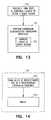
- FIG. 13illustrates a process for forming semiconductor devices, according to various embodiments of the present invention.
- FIG. 14illustrates a process for precisely forming voids in a substrate located to getter a device region as performed in the process for forming semiconductor devices of FIG. 13 .
- FIG. 15is a simplified block diagram of a high-level organization of a memory device, according to various embodiments of the present invention.
- FIG. 16is a simplified block diagram of a high-level organization of an electronic system, according to various embodiments of the present invention.
- wafer and substrateare interchangeably used to refer generally to any structure on which integrated circuits are formed, and also to such structures during various stages of integrated circuit fabrication. Both terms include doped and undoped semiconductors, epitaxial layers of a semiconductor on a supporting semiconductor or insulating material, combinations of such layers, as well as other such structures that are known in the art.
- aspects of the present inventionprecisely form voids at desired location using a surface transformation process to getter semiconductor wafers.
- Various embodimentsprecisely form patterns of nano-voids (voids having a diameter on the order of a nanometer) as a proximity gettering region to effectively and consistently getter impurities from device regions.
- FIG. 1illustrates a semiconductor structure having a gettering region with precisely formed voids at precise locations, according to various embodiments of the present invention.
- the illustrated structure 100includes a semiconductor wafer, also referred to here as a substrate 101 .
- a proximity gettering region 102is located near to a device region 103 such that unwanted impurities can travel a short distance from the device region 103 to the gettering region 102 , even with modern low temperature processes.
- the gettering region 102includes a number of precisely formed and located voids 104 formed by surface transformation. Surface transformation is described in detail below.
- the present inventionis not limited to gettering regions having a particular pattern, shape or size of voids.
- the device region 103includes crystalline silicon.
- Semiconductor devicessuch as transistors, are fabricated in the crystalline silicon. Other crystalline semiconductor materials can be used to form the device region 103 . Thus, it is desired to getter unwanted impurities from the device region.
- the voids 104 in the gettering region 102generate defects that getter impurities from the device region 103 .
- the internal surfaces of the voidshave numerous dangling bonds, and thus are highly chemically reactive, which serves to getter impurities from the device region 103 .
- FIG. 2illustrates a semiconductor structure having a gettering region with precisely formed voids at precise locations, according to various embodiments of the present invention.
- the illustrated structure 200includes a semiconductor wafer, also referred to here as a substrate 201 .
- a number of proximity gettering regions 202are located near to a number of device regions 203 such that unwanted impurities can travel a short distance from the device regions 203 to the gettering regions 202 , even with modern low temperature processes.
- the gettering region 202includes a number of precisely formed and located voids 204 .
- the present inventionis not limited to gettering regions having the illustrated pattern, size or shape of voids.
- the voidscreate defects that are highly chemically reactive and serve to getter impurities from the device region 203 .
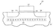
- FIG. 3illustrates a transistor formed in a device region proximate to a gettering region with precisely formed voids at precise locations, according to various embodiments of the present invention.
- the illustrated transistor 305is fabricated over a proximity gettering region 302 .
- the gettering region 302has a predetermined and precise arrangement of precisely formed voids 304 .
- a gate oxide 306is formed on the substrate 301 , and a gate is formed over the gate oxide.
- First and second diffusion regions 308 and 309are formed.
- a transistor channel region 310is formed between the first and second diffusion regions 308 and 309 .
- Other devicessuch as capacitors and diodes, can be formed in device regions proximate to a gettering region.
- These gettering regions and device regionscan be formed in both bulk and semiconductor-on-insulator (SOI) technology. Furthermore, these gettering regions can be used to getter both strained and unstrained device regions.
- SOIsemiconductor-on-insulator
- the precisely-determined arrangement of voidsprovides the gettering region with voids that are more uniformly spaced and with a majority of voids that are closed voids.
- the uniformity, density, and space symmetry of the voids in the gettering regionis precisely determined by controlling the diameter, depth and position of an initial arrangement of cylindrical holes formed through a surface of a solid (e.g. a surface of a semiconductor wafer).
- the holeshave a generally-elongated shape extending into the volume away from the surface.
- the holeshave a generally cylindrical shape. The present subject matter is not so limited, however.
- the voids in the gettering regiongenerate defects that getter impurities from the device region.
- the internal surfaces of the voidshave numerous dangling bonds, and thus are highly chemically reactive which serves to getter impurities from the device region.
- various embodiments for voids and voids patternsto have a large surface to volume ratio to increase the gettering of impurities.
- the precisely-determined arrangement of voidsprovides the semiconductor wafer with a predictable mechanical failure for a given force.
- the precisely-determined arrangement of voidsprovides the semiconductor wafer with an anisotropic stiffness.
- holesWhen a solid is heated to a higher temperature, a solid with a hole that is beyond a critical length ( ⁇ c ) becomes unstable.
- ⁇ ccritical length
- the holesare referred to as cylindrical holes.
- the cylindrical holeis transformed into one or more empty spheres formed along the cylinder axis.
- the number (N) of spheres formeddepends on the length (L) and radius (R C ) of the cylinder.
- Two models of diffusionare the surface diffusion model and the pure volume diffusion model. With respect to the surface diffusion model, for example, the relation between the cylinder length (L), cylinder radius (R C ), and number of spheres (N) is expressed by the following equation: 8.89 ⁇ R C ⁇ N ⁇ L ⁇ 8.89 ⁇ R C ⁇ ( N+ 1). (1) Equation (1) predicts that no empty spheres will form if L ⁇ 8.89 ⁇ R C .
- the pure volume diffusion modelprovides similar results, with slightly different constants. For example, depending on the exact magnitude of the diffusion parameters, ⁇ C can vary from 9.02 ⁇ R C to 12.96 ⁇ R C .
- ⁇ Ccan vary from 9.02 ⁇ R C to 12.96 ⁇ R C .
- the diffusion modelis capable of being determined by experiment. The remainder of this disclosure uses the surface diffusion model.
- One of ordinary skill in the artwill understand, upon reading and comprehending this disclosure, how to apply this disclosure to another diffusion model.
- Various shaped empty spaces or voidssuch as sphere-shaped voids, pipe-shaped voids, and plate-shaped voids are capable of being formed under the surface of a semiconductor substrate or wafer with a well-defined melting temperature.
- the shape of the empty spaces formed during the annealing conditionsdepends on the size, number and spacing of the cylindrical holes that are initially formed at a lower temperature.
- Various predetermined arrangements of empty spaces or voidsare capable of being formed under the surface of a semiconductor substrate or wafer with a well-defined melting temperature. For example, an appropriately-sized deep trench in a material with a well-defined melting temperature is transformed into empty spheres along the axis of the original trench at an annealing temperature within a predetermined a range below the melting temperature. The empty spheres are uniformly sized and spaced. Other predetermined arrangements are provided below.
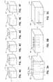
- FIGS. 4A-4Fillustrate a process to form a sphere-shaped empty space in a gettering region, according to various embodiments of the present invention.
- a cylindrical hole 411is formed through the surface 412 of a semiconductor volume where at least part of the volume forms a gettering region 402 .
- the term holerefers to a void that extends from a surface of the volume into the solid material and that is defined by the solid material.
- the semiconductor volume 402is heated (annealed) and undergoes the transformation illustrated in FIGS. 4B through 4F .
- the desired annealing temperatureis dependent on the well-defined melting temperature of the semiconductor material.
- the result of the surface transformation processis an empty sphere 413 formed below the surface 412 of the semiconductor volume 402 .
- the center-to-center spacing (D NT ) between the initial cylindrical holeswill satisfy the following equation: 2 ⁇ R C ⁇ D NT ⁇ 3.76 ⁇ R C . (4) Satisfying this equation prevents the adjacent initial cylindrical holes from touching, yet allows the adjacent surface-transformed spheres to combine and form pipe and plate empty spaces, as shown in FIGS. 5A-5C and FIGS. 6A-6B and described below.
- FIGS. 5A-5Cillustrate a process to form a pipe-shaped empty space in a gettering region, according to various embodiments of the present invention.
- a linear array of cylindrical holes 511is formed through a surface 512 of a semiconductor volume where at least part of the volume forms a gettering region 502 .
- the cylindrical holes 511have a center-to-center spacing (D NT ) as calculated using equation (4).
- the semiconductor material 502is heated (annealed) and undergoes the transformation illustrated in FIGS. 5B through 5C .
- the result of the surface transformation processis an empty pipe-shaped void 514 formed below the surface 512 of the semiconductor volume 502 .
- FIGS. 6A-6Billustrate a process to form a plate-shaped empty space in a gettering region, according to various embodiments of the present invention.
- a two-dimensional array of cylindrical holes 611is formed in a surface 612 of a semiconductor volume where at least part of the volume forms a gettering region 602 .
- the cylindrical holes 611have a center-to-center spacing (D NT ) as calculated using equation (4).
- the material 602is heated (annealed) and undergoes the transformation illustrated in FIGS. 6B .
- the result of the surface transformation processis an empty plate-shaped void 615 formed below the surface 612 of the volume of material 602 .
- the voidsare formed in a gettering region using surface transformation.
- a precisely-determined arrangement of voidsis formed using surface transformation to provide a large interior void surface to volume ratio and to provide a desired distribution of the voids throughout the gettering region.
- the voids in the gettering regioninclude nano-sized voids (“nano-voids”).
- the present subject matterforms a precisely-determined arrangement of voids using surface transformation to provide a cellular material with a predictable mechanical failure for a given force.
- the present subject matterforms a precisely-determined arrangement of voids using surface transformation to provide a cellular material with an anisotropic stiffness.
- the size, shape and spacing of empty spacesis controlled by the diameter, depth and spacing of holes (or trenches) initially formed in a semiconductor material that has a defined melting temperature.
- Empty spaces or voidsare formed after annealing the material in a temperature range below and near the defined melting temperature.
- the empty spaces or voidsare capable of being formed with a spherical shape, a pipe shape, plate shape, various combinations of these shape types, and/or various dimensions for the various shape type and combinations of shape type.
- the volume of air incorporated in the surface transformed empty spacesis equal to the volume of air within the initial starting pattern of cylindrical holes. Thus, the surface transformed empty spaces do not cause additional stress in the material or a tendency for the material to crack.
- the surface of the semiconductor volumewill be smooth after the surface transformed empty spaces are formed if the initial cylinder length (L) is equal to an integer of a critical length ( ⁇ c ) such as 1 ⁇ c to form one sphere, 2 ⁇ c to form two spheres, 3 ⁇ c to form three spheres, etc. If the cylinder length (L) is not equal to an integer of a critical length ( ⁇ c ), then the surface will have dimples caused by air in the cylinder attributable to the length beyond an integer of a critical length ( ⁇ c ). That is, for a given length L and ⁇ c , the number of spheres formed is the integer of L/ ⁇ c , and the remainder of L/ ⁇ c contributes to the dimples on the surface.
- a critical length⁇ c
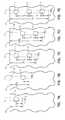
- FIGS. 7A-7Eillustrate the formation of empty spheres in a gettering region from initial cylindrical holes with the same radii and with varying length, according to various embodiments of the present invention.
- Initial cylindrical holesare represented using dashed lines 711 .
- These initial cylindrical holes 711have the same radius (R C ) and are drilled or otherwise formed to different depths as represented by FIGS. 7A, 7B , 7 C, 7 D and 7 E.
- the resulting surface-transformed spheres 713are illustrated with a solid line, as are the surface dimples 716 that form when the cylindrical hole depth is not an integer multiple of ⁇ C .
- These surface dimplescan be removed using a simple polishing process to leave a smooth surface with uniform and closed spherical voids within the material.
- a crystalline semiconductorcan be formed over the polished gettering region for use in fabricating semiconductor devices. The vertical position and number of the spherical voids is determined by the depth of the initial cylindrical holes.
- the gettering region of the semiconductor substrateis formed by appropriately spacing the initially-formed holes such that, upon annealing the semiconductor material to provide the surface transformation process, the resulting voids are uniformly spaced (or approximately uniformly spaced) throughout the gettering region.
- the uniformly spaced voidsprovide the gettering region with the ability to getter a device region with more uniformity. Smaller voids provide more gettering uniformity. With more predictable gettering of device regions, the performance of the devices formed therein is more predictable, thus providing better yield.
- a gettering region with voidsit is desirable to provide a gettering region with voids to provide a high internal void surface to volume ratio to improve gettering.
- the interior void surfaceshave dangling bonds that are highly chemically reactive, and are useful to getter impurities.
- FIG. 8illustrates a transformation formed stack of empty plates 815 in a gettering region 802 , according to various embodiments of the present invention.
- the illustrated filling factor, fis approximately equal to 0.78, which provides a relatively high porosity, a relatively low density, and a relatively high internal void surface to volume ratio.
- the surface transformationproduces a vertical stack of empty plates in the materials. The number of empty plates formed depends on the length of the holes.
- a plurality of space group symmetries of empty spheres of equal sizeare formed in a solid material.
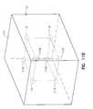
- FIG. 9illustrates fourteen representative unit cells of space lattices which the voids in the gettering region can form, according to various embodiments of the present invention.
- a 0lattice constant
- FIG. 9illustrates fourteen representative unit cells of space lattices which the voids in the gettering region can form, according to various embodiments of the present invention.
- Each void in the unit cellcan be the same shape (e.g. sphere-shaped, plate-shaped or pipe-shaped voids).
- the unit cellincludes different combinations of sphere-shaped, plate-shaped, or pipe-shaped voids.
- FIG. 10illustrates a void pattern in a gettering region arranged to form the cubic P unit cell shown among the fourteen representative unit cells of FIG. 9 .
- a defined set of cylindrical holesare drilled or otherwise formed into the gettering region to form empty spheres 1013 of the same radius in the solid material at each of the illustrated unit cell lattice positions.
- the formation of one unit cell in the x-y plane and n unit cells in the z directionis discussed. Additional unit cells in the x-y planes are formed by repeatedly translating the hole pattern for the unit cell in the x and y directions.
- FIGS. 11A-11Billustrate a process for forming a cubic P lattice of spherical empty spaces, according to various embodiments of the present invention.
- the four cylindrical holes 1111 A, 1111 B, 1111 C and 1111 Dare spaced apart along the x and y axes at a distance a 0 .
- the solid materialis annealed near its melting temperature to form sphere-shaped empty spaces 1113 A, 1113 B, 1113 C, 1113 D, 1113 E, 1113 F, 1113 G and 1113 H by surface transformation at desired sites of the cubic P unit cell as is shown in FIG. 11B .
- each primitive lattice in FIG. 6can be formed to have equal sized empty spheres at each lattice site by forming in the Z direction an appropriate pattern of cylindrical holes of the same diameter in the x-y plane. The prescribed depths for these unit cells will generally be different.
- space lattices having more than one size of empty spheres in the unit cellare formed by forming initial cylindrical holes of more than one radius. In various embodiments, the holes are formed in more than one direction. The number of surface transformation annealing steps used to form the space lattice depends on the structure to be formed. A method to form a simple illustrative structural unit of empty spheres is described below.
- FIGS. 12A-12Dillustrate a process for forming a simple unit of empty spheres having two radii in a gettering region, according to various embodiments of the present invention.
- the process to form the above-described structureis illustrated in FIGS. 12A, 12B , 12 C and 12 D.
- FIG. 12DAnother method for forming the structure in FIG. 12D involves forming the cellular material in various deposition layers and forming the voids using a surface transformation process (i.e. hole formation and annealing) for each layer before a successive layer of material is deposited.
- a surface transformation processi.e. hole formation and annealing
- the structure illustrated in FIG. 12Dis formed by a first deposition process, a first surface transformation process, a second deposition process, a second surface transformation process, a third deposition process, a third surface transformation process, a fourth deposition process, and a fourth surface transformation process.
- Each surface transformation stepincludes hole formation and annealing.
- the hole formation patternis calculated to achieve the desired spacing of resulting voids, both between and within layers, after the layer is annealed.
- a cellular materialcan include a number of sphere-shaped voids, a number of pipe-shaped voids, a number of plate-shaped voids, and various combinations of sphere-shaped void(s), pipe-shaped void(s), and plate-shaped void(s).
- each stack of voidscan include various shapes.
- the precisely-determined arrangement of empty spacesis determined by the position, depth and diameter of the holes formed prior to the annealing process.
- FIG. 13illustrates a process for forming semiconductor devices, according to various embodiments of the present invention.
- voidsare precisely formed and are located to getter a device region.
- subsequent semiconductor fabrication processesare performed, As represented at 1322 , these subsequent semiconductor fabrication processes include forming a semiconductor device in a device region.
- An example of a semiconductor deviceis a transistor.
- these semiconductor processesinclude depositing a semiconductor such as crystalline silicon on the gettering region, and forming a transistor using the crystalline silicon.
- the voidsare formed in a crystalline semiconductor volume, and the devices are formed using the crystalline semiconductor above the voids.
- the voidsare formed in a crystalline semiconductor volume, and the devices are formed using the crystalline semiconductor adjacent to the voids.
- FIG. 14illustrates a process for precisely forming voids in a substrate located to getter a device region as performed in the process for forming semiconductor devices of FIG. 13 .
- the illustrated process 1420generally corresponds to the 1320 in FIG. 13 .
- holesare formed to extend from a substrate surface and into a semiconductor substrate at 1423 .
- the holeshave a predetermined size and shape, and are formed in a predetermined location or pattern of locations in the substrate.
- the holeshave a generally cylindrical shape.
- the substrateis annealed to form predetermined voids in the substrate.
- the substratehas a well-defined melting temperature, and the annealing temperature is slightly below the melting temperature.
- the voidscan include sphere-shape voids, a pipe-shape voids and/or plate-shaped voids.
- the present subject matterprovides the ability to form gettering regions with a precisely-determined arrangement of precisely-formed voids using surface transformation.
- the precisely-determined arrangement of precisely-formed voidsinclude uniformly spaced and closed voids that provide the gettering region with uniform gettering characteristics and with a large internal surface to volume ratio to provide a large number of uniformly distributed dangling bonds (defects in the crystalline structure) in proximity to a device region to effectively getter the device region.
- semiconductor devicesare cable of being precisely fabricated.
- FIG. 15is a simplified block diagram of a high-level organization of a memory device, according to various embodiments of the present invention.
- the illustrated memory device 1530includes a memory array 1531 and read/write control circuitry 1532 to perform operations on the memory array via communication line(s) 1533 .
- the illustrated memory device 1530may be a memory card or a memory module such as a single inline memory module (SIMM) and dual inline memory module (DIMM).
- SIMMsingle inline memory module
- DIMMdual inline memory module
- the memory array 1531includes a number of memory cells 1534 .
- the memory cells in the arrayare arranged in rows and columns.
- word lines 1535connect the memory cells in the rows
- bit lines 1536connect the memory cells in the columns.
- the read/write control circuitry 1532includes word line select circuitry 1537 , which functions to select a desired row.
- the read/write control circuitry 1532further includes bit line select circuitry 1538 , which functions to select a desired column.
- FIG. 16is a simplified block diagram of a high-level organization of an electronic system, according to various embodiments of the present invention.
- the system 1640is a computer system, a process control system or other system that employs a processor and associated memory.
- the electronic system 1640has functional elements, including a processor or arithmetic/logic unit (ALU) 1641 , a control unit 1642 , a memory device unit 1643 (such as illustrated at 1530 in FIG. 15 ) and an input/output (I/O) device 1644 .
- ALUarithmetic/logic unit
- the control unit 1642coordinates all operations of the processor 1641 , the memory device 1643 and the I/O devices 1644 by continuously cycling through a set of operations that cause instructions to be fetched from the memory device 1643 and executed.
- the memory device 1643includes, but is not limited to, random access memory (RAM) devices, read-only memory (ROM) devices, and peripheral devices such as a floppy disk drive and a compact disk CD-ROM drive.
- RAMrandom access memory
- ROMread-only memory
- peripheral devicessuch as a floppy disk drive and a compact disk CD-ROM drive.
- the illustration of the system 1640is intended to provide a general understanding of one application for the structure and circuitry, and is not intended to serve as a complete description of all the elements and features of an electronic system using proximity gettering regions according to the various embodiments of the present invention.
- an electronic systemcan be fabricated in single-package processing units, or even on a single semiconductor chip, in order to reduce the communication time between the processor and the memory device.
- Applications containing a gettering region as described in this disclosureinclude electronic systems for use in memory modules, device drivers, power modules, communication modems, processor modules, and application-specific modules, and may include multilayer, multichip modules. Such circuitry can further be a subcomponent of a variety of electronic systems.
- Various embodiments disclosed hereingetter a semiconductor wafer by precisely forming voids, such as nano-voids, at desired locations in the wafers. Various embodiments form an even distribution of voids across the wafer below device regions. In various embodiments, precisely-formed gettering void patterns are formed proximate to selected regions where devices are fabricated on the semiconductor wafer. Various embodiments precisely form the void patterns below device regions. Numerous dangling bonds are present at the internal surfaces of the voids such that these internal surfaces are highly chemically reactive. Thus, various embodiments form the voids and void patterns to have the greatest surface to volume ratio to increase the gettering of impurities.
Landscapes
- Engineering & Computer Science (AREA)
- Physics & Mathematics (AREA)
- Condensed Matter Physics & Semiconductors (AREA)
- General Physics & Mathematics (AREA)
- Manufacturing & Machinery (AREA)
- Computer Hardware Design (AREA)
- Microelectronics & Electronic Packaging (AREA)
- Power Engineering (AREA)
- Insulated Gate Type Field-Effect Transistor (AREA)
- Semiconductor Memories (AREA)
- Non-Volatile Memory (AREA)
Abstract
Description
- The present application is a continuation of U.S. application Ser. No. 10/623,794, filed Jul. 21, 2003, which is incorporated herein by reference.
- This application is related to the following commonly assigned U.S. patent applications which are herein incorporated by reference in their entirety: “Cellular Materials Formed Using Surface Transformation,” application Ser. No. 10/382,246, filed Mar. 5, 2003; “Gettering of Silicon On Insulator Using Relaxed Silicon Germanium Epitaxial Proximity Layers,” application Ser. No. 10/443,337, filed May 21, 2003; and “Wafer Gettering Using Relaxed Silicon Germanium Epitaxial Proximity Layers,” application Ser. No. 10/443,339, filed May 21, 2003.
- This disclosure relates generally to integrated circuits, and more particularly, to strained semiconductor structures.
- Unwanted crystalline defects and impurities can be introduced during crystal growth or subsequent wafer fabrication processes. These defect and impurities can degrade device characteristics and overall yield. Gettering has been described as a process for moving contaminants and/or defects in a semiconductor into its bulk and away from its top surface to create a denuded zone cleared from contaminants and/or defects. Preferably, devices are built in the denuded zone.
- Historically, extrinsic backside gettering was used to getter silicon wafers. Various extrinsic backside gettering processes involve damaging the backside of the wafer mechanically or by implanting argon, germanium, hydrogen or other implants, or providing a gettering layer on the backside of the wafer using a phophorosilicate glass or oxide backside layer, a polysilicon backside layer, and a silicon germanium (SiGe) backside epitaxial layer. Subsequently, “intrinsic” gettering was developed, which employed oxygen precipitation and “bulk microdefects” precipitated into the bulk of the wafer after the surface was “denuded” of oxygen. The precipitation process, the gettering effects, and the electrical characterization of defects and gettering silicon wafers have been investigated. Recently, intrinsic gettering modifications have been developed, including neutron irradiation, high boron doping, nitrogen doping, and the use of magnetic fields during crystal growth.
- These gettering processes depend on the diffusion of unwanted impurities over significant distances from desired device regions to the gettering sites. However, modern low temperature processes have small thermal budgets, and do not afford an opportunity for significant diffusion of dopants and/or unwanted impurities. Thus, it is desirable to reduce the distance between the gettering sites and the device area. It has been previously proposed to implant various impurities in proximity to the device areas, to co-implant oxygen and silicon to form a gettering layer in close proximity to the device area, to implant helium to form cavities close to the device areas which getter impurities, and to getter material in trench isolation areas in close proximity to the device areas.
- Implanting helium forms cavities that function to getter impurities. This helium implantation technique has been proposed to getter both bulk and silicon-on-insulator devices. However, the location and density of these cavities formed by implanting helium is random. One problem associated with the random location and density of cavities is that the effectiveness of the gettering unwanted impurities from the desired device regions is inconsistent. Other problems associated with the random location and density of cavities involves the varying strain in the substrate and the varying ability of the substrate to withstand mechanical strain. The inconsistent effectiveness of gettering, the inconsistent strain and the inconsistent ability to withstand strain can negatively affect the ability to precisely form devices as the semiconductor industry strives to fabricate smaller and thinner devices.
- The above mentioned problems are addressed and will be understood by reading and studying this specification. Various aspects and embodiments of the present invention getter a semiconductor wafer by precisely forming voids, such as nano-sized voids, at desired locations in the wafers. Thus, precisely-formed gettering void patterns are formed in selected regions below where devices are fabricated on semiconductor wafers. Numerous dangling bonds are present at the internal surfaces of the voids such that these internal surfaces are highly chemically reactive. Thus, various embodiments form the voids and void patterns to have a large surface to volume ratio to increase gettering of impurities.
- One aspect of this disclosure relates to a method for creating a gettering site in a semiconductor wafer. In various embodiments, a predetermined arrangement of a plurality of holes is formed in the semiconductor wafer through a surface of the wafer. The wafer is annealed such that the wafer undergoes a surface transformation to transform the arrangement of the plurality of holes into a predetermined arrangement of at least one empty space of a predetermined size within the wafer to form the gettering site.
- One aspect relates to a semiconductor wafer. In various embodiments, the wafer includes at least one device region, and at least one gettering region located proximate to the at least one device region. The gettering region includes a precisely-determined arrangement of a plurality of precisely-formed voids that are formed within the wafer using a surface transformation process. Other aspects and embodiments are provided herein.
- This Summary is an overview of some of the teachings of the present application and not intended to be an exclusive or exhaustive treatment of the present subject matter. Further details are found in the detailed description and appended claims. Other aspects will be apparent to persons skilled in the art upon reading and understanding the following detailed description and viewing the drawings that form a part thereof, each of which are not to be taken in a limiting sense. The scope of the present invention is defined by the appended claims and their legal equivalents.
FIG. 1 illustrates a semiconductor structure having a gettering region with precisely formed voids at precise locations, according to various embodiments of the present invention.FIG. 2 illustrates a semiconductor structure having a gettering region with precisely formed voids at precise locations, according to various embodiments of the present invention.FIG. 3 illustrates a transistor formed in a device region proximate to a gettering region with precisely formed voids at precise locations, according to various embodiments of the present invention.FIGS. 4A-4F illustrate a process to form a sphere-shaped empty space in a gettering region, according to various embodiments of the present invention.FIGS. 5A-5C illustrate a process to form a pipe-shaped empty space in a gettering region, according to various embodiments of the present invention.FIGS. 6A-6B illustrate a process to form a plate-shaped empty space in a gettering region, according to various embodiments of the present invention.FIGS. 7A-7E illustrate the formation of empty spheres in a gettering region from initial cylindrical holes with the same radii and with varying length, according to various embodiments of the present invention.FIG. 8 illustrates a transformation formed stack of empty plates in a gettering region, according to various embodiments of the present invention.FIG. 9 illustrates fourteen representative unit cells of space lattices which the voids in the gettering region can form, according to various embodiments of the present invention.FIG. 10 illustrates a void pattern in a gettering region arranged to form the cubic P unit cell shown among the fourteen representative unit cells ofFIG. 9 .FIGS. 11A-11B illustrate a process for forming a cubic P lattice of spherical empty spaces, according to various embodiments of the present invention.FIGS. 12A-12D illustrate a process for forming a simple unit of empty spheres having two radii in a gettering region, according to various embodiments of the present invention.FIG. 13 illustrates a process for forming semiconductor devices, according to various embodiments of the present invention.FIG. 14 illustrates a process for precisely forming voids in a substrate located to getter a device region as performed in the process for forming semiconductor devices ofFIG. 13 .FIG. 15 is a simplified block diagram of a high-level organization of a memory device, according to various embodiments of the present invention.FIG. 16 is a simplified block diagram of a high-level organization of an electronic system, according to various embodiments of the present invention.- The following detailed description refers to the accompanying drawings which show, by way of illustration, specific aspects and embodiments in which the present invention may be practiced. The various embodiments are not necessarily mutually exclusive as aspects of one embodiment can be combined with aspects of another embodiment. Other embodiments may be utilized and structural, logical, and electrical changes may be made without departing from the scope of the present invention. In the following description, the terms wafer and substrate are interchangeably used to refer generally to any structure on which integrated circuits are formed, and also to such structures during various stages of integrated circuit fabrication. Both terms include doped and undoped semiconductors, epitaxial layers of a semiconductor on a supporting semiconductor or insulating material, combinations of such layers, as well as other such structures that are known in the art. The terms “horizontal” and “vertical”, as well as prepositions such as “on”, “over” and “under” are used in relation to the conventional plane or surface of a wafer or substrate, regardless of the orientation of the wafer or substrate. References to “an”, “one”, or “various” embodiments in this disclosure are not necessarily to the same embodiment, and such references contemplate more than one embodiment. The following detailed description is, therefore, not to be taken in a limiting sense, and the scope of the present invention is defined only by the appended claims, along with the full scope of equivalents to which such claims are entitled.
- Aspects of the present invention precisely form voids at desired location using a surface transformation process to getter semiconductor wafers. Various embodiments precisely form patterns of nano-voids (voids having a diameter on the order of a nanometer) as a proximity gettering region to effectively and consistently getter impurities from device regions.
FIG. 1 illustrates a semiconductor structure having a gettering region with precisely formed voids at precise locations, according to various embodiments of the present invention. The illustratedstructure 100 includes a semiconductor wafer, also referred to here as asubstrate 101. A proximity gettering region102 is located near to adevice region 103 such that unwanted impurities can travel a short distance from thedevice region 103 to the gettering region102, even with modern low temperature processes. The gettering region102 includes a number of precisely formed and located voids104 formed by surface transformation. Surface transformation is described in detail below. The present invention is not limited to gettering regions having a particular pattern, shape or size of voids. In various embodiments, thedevice region 103 includes crystalline silicon. Semiconductor devices, such as transistors, are fabricated in the crystalline silicon. Other crystalline semiconductor materials can be used to form thedevice region 103. Thus, it is desired to getter unwanted impurities from the device region. The voids104 in the gettering region102 generate defects that getter impurities from thedevice region 103. The internal surfaces of the voids have numerous dangling bonds, and thus are highly chemically reactive, which serves to getter impurities from thedevice region 103.FIG. 2 illustrates a semiconductor structure having a gettering region with precisely formed voids at precise locations, according to various embodiments of the present invention. The illustratedstructure 200 includes a semiconductor wafer, also referred to here as asubstrate 201. A number ofproximity gettering regions 202 are located near to a number ofdevice regions 203 such that unwanted impurities can travel a short distance from thedevice regions 203 to thegettering regions 202, even with modern low temperature processes. Thegettering region 202 includes a number of precisely formed and locatedvoids 204. The present invention is not limited to gettering regions having the illustrated pattern, size or shape of voids. The voids create defects that are highly chemically reactive and serve to getter impurities from thedevice region 203.FIG. 3 illustrates a transistor formed in a device region proximate to a gettering region with precisely formed voids at precise locations, according to various embodiments of the present invention. The illustratedtransistor 305 is fabricated over aproximity gettering region 302. Thegettering region 302 has a predetermined and precise arrangement of precisely formed voids304. Agate oxide 306 is formed on thesubstrate 301, and a gate is formed over the gate oxide. First andsecond diffusion regions transistor channel region 310 is formed between the first andsecond diffusion regions - In various embodiments, the precisely-determined arrangement of voids provides the gettering region with voids that are more uniformly spaced and with a majority of voids that are closed voids. The uniformity, density, and space symmetry of the voids in the gettering region is precisely determined by controlling the diameter, depth and position of an initial arrangement of cylindrical holes formed through a surface of a solid (e.g. a surface of a semiconductor wafer). In various embodiments, the holes have a generally-elongated shape extending into the volume away from the surface. In various embodiments, the holes have a generally cylindrical shape. The present subject matter is not so limited, however.
- The voids in the gettering region generate defects that getter impurities from the device region. The internal surfaces of the voids have numerous dangling bonds, and thus are highly chemically reactive which serves to getter impurities from the device region. Thus, various embodiments for voids and voids patterns to have a large surface to volume ratio to increase the gettering of impurities. In various embodiments, the precisely-determined arrangement of voids provides the semiconductor wafer with a predictable mechanical failure for a given force. In various embodiments, the precisely-determined arrangement of voids provides the semiconductor wafer with an anisotropic stiffness.
- When a solid is heated to a higher temperature, a solid with a hole that is beyond a critical length (λc) becomes unstable. For the purposes of the analysis provided below, the holes are referred to as cylindrical holes. Upon reading and comprehending this disclosure, one of ordinary skill in the art will understand that holes which are not geometrically cylindrical can be used in a surface transformation process, and further will understand how to form a predetermined arrangement of voids using holes that are not geometrically cylindrical.
- The cylindrical hole is transformed into one or more empty spheres formed along the cylinder axis. The number (N) of spheres formed depends on the length (L) and radius (RC) of the cylinder. Two models of diffusion are the surface diffusion model and the pure volume diffusion model. With respect to the surface diffusion model, for example, the relation between the cylinder length (L), cylinder radius (RC), and number of spheres (N) is expressed by the following equation:
8.89×RC×N≦L<8.89×RC×(N+1). (1)
Equation (1) predicts that no empty spheres will form if L<8.89×RC. Each empty sphere that forms has a radius (RS) expressed by the following equation:
RS=1.88×RC. (2)
If the cylinder has sufficient length L to form two spheres, the center-to-center spacing between the spheres corresponds to the critical length (λC) and is provided by the equation:
λC=8.89×RC. (3)
The pure volume diffusion model provides similar results, with slightly different constants. For example, depending on the exact magnitude of the diffusion parameters, λCcan vary from 9.02×RCto 12.96×RC. One of ordinary skill in the art will understand, upon reading and understanding this disclosure, that the diffusion model is capable of being determined by experiment. The remainder of this disclosure uses the surface diffusion model. One of ordinary skill in the art will understand, upon reading and comprehending this disclosure, how to apply this disclosure to another diffusion model. - Various shaped empty spaces or voids such as sphere-shaped voids, pipe-shaped voids, and plate-shaped voids are capable of being formed under the surface of a semiconductor substrate or wafer with a well-defined melting temperature. The shape of the empty spaces formed during the annealing conditions depends on the size, number and spacing of the cylindrical holes that are initially formed at a lower temperature.
- Various predetermined arrangements of empty spaces or voids are capable of being formed under the surface of a semiconductor substrate or wafer with a well-defined melting temperature. For example, an appropriately-sized deep trench in a material with a well-defined melting temperature is transformed into empty spheres along the axis of the original trench at an annealing temperature within a predetermined a range below the melting temperature. The empty spheres are uniformly sized and spaced. Other predetermined arrangements are provided below.
FIGS. 4A-4F illustrate a process to form a sphere-shaped empty space in a gettering region, according to various embodiments of the present invention. Acylindrical hole 411 is formed through thesurface 412 of a semiconductor volume where at least part of the volume forms agettering region 402. As used here, the term hole refers to a void that extends from a surface of the volume into the solid material and that is defined by the solid material. Thesemiconductor volume 402 is heated (annealed) and undergoes the transformation illustrated inFIGS. 4B through 4F . One of ordinary skill in the art would understand, upon reading and comprehending this disclosure, that the desired annealing temperature is dependent on the well-defined melting temperature of the semiconductor material. The result of the surface transformation process is anempty sphere 413 formed below thesurface 412 of thesemiconductor volume 402.- In order to form a single sphere, which holds true for forming a single pipe (
FIGS. 5A-5C ) or plate (FIGS. 6A-6B ), the length (L) and radius (RC) of the cylindrical holes are chosen such that equation (1) with N=1 is satisfied. A vertical stacking of N empty spaces results if the length of the cylindrical holes is such that equation (1) is satisfied. - In order for single surface-transformed spheres to combine with other surface-transformed spheres, the center-to-center spacing (DNT) between the initial cylindrical holes will satisfy the following equation:
2×RC<DNT<3.76×RC. (4)
Satisfying this equation prevents the adjacent initial cylindrical holes from touching, yet allows the adjacent surface-transformed spheres to combine and form pipe and plate empty spaces, as shown inFIGS. 5A-5C andFIGS. 6A-6B and described below. FIGS. 5A-5C illustrate a process to form a pipe-shaped empty space in a gettering region, according to various embodiments of the present invention. A linear array of cylindrical holes511 is formed through asurface 512 of a semiconductor volume where at least part of the volume forms agettering region 502. The cylindrical holes511 have a center-to-center spacing (DNT) as calculated using equation (4). Thesemiconductor material 502 is heated (annealed) and undergoes the transformation illustrated inFIGS. 5B through 5C . The result of the surface transformation process is an empty pipe-shapedvoid 514 formed below thesurface 512 of thesemiconductor volume 502. The radius (RP) of the pipe-shapedvoid 514 is provided by the following equation:FIGS. 6A-6B illustrate a process to form a plate-shaped empty space in a gettering region, according to various embodiments of the present invention. A two-dimensional array ofcylindrical holes 611 is formed in asurface 612 of a semiconductor volume where at least part of the volume forms agettering region 602. Thecylindrical holes 611 have a center-to-center spacing (DNT) as calculated using equation (4). Thematerial 602 is heated (annealed) and undergoes the transformation illustrated inFIGS. 6B . The result of the surface transformation process is an empty plate-shapedvoid 615 formed below thesurface 612 of the volume ofmaterial 602. The thickness (TP) of a plate320 is given by the following equation:- The voids are formed in a gettering region using surface transformation. In various embodiments, a precisely-determined arrangement of voids is formed using surface transformation to provide a large interior void surface to volume ratio and to provide a desired distribution of the voids throughout the gettering region. In various embodiments, the voids in the gettering region include nano-sized voids (“nano-voids”). In various embodiments, the present subject matter forms a precisely-determined arrangement of voids using surface transformation to provide a cellular material with a predictable mechanical failure for a given force. In various embodiments, the present subject matter forms a precisely-determined arrangement of voids using surface transformation to provide a cellular material with an anisotropic stiffness.
- The size, shape and spacing of empty spaces is controlled by the diameter, depth and spacing of holes (or trenches) initially formed in a semiconductor material that has a defined melting temperature. Empty spaces or voids are formed after annealing the material in a temperature range below and near the defined melting temperature. The empty spaces or voids are capable of being formed with a spherical shape, a pipe shape, plate shape, various combinations of these shape types, and/or various dimensions for the various shape type and combinations of shape type. The volume of air incorporated in the surface transformed empty spaces is equal to the volume of air within the initial starting pattern of cylindrical holes. Thus, the surface transformed empty spaces do not cause additional stress in the material or a tendency for the material to crack.
- The surface of the semiconductor volume will be smooth after the surface transformed empty spaces are formed if the initial cylinder length (L) is equal to an integer of a critical length (λc) such as 1×λcto form one sphere, 2×λcto form two spheres, 3×λcto form three spheres, etc. If the cylinder length (L) is not equal to an integer of a critical length (λc), then the surface will have dimples caused by air in the cylinder attributable to the length beyond an integer of a critical length (λc). That is, for a given length L and λc, the number of spheres formed is the integer of L/λc, and the remainder of L/λccontributes to the dimples on the surface.
FIGS. 7A-7E illustrate the formation of empty spheres in a gettering region from initial cylindrical holes with the same radii and with varying length, according to various embodiments of the present invention. Initial cylindrical holes are represented using dashedlines 711. These initialcylindrical holes 711 have the same radius (RC) and are drilled or otherwise formed to different depths as represented byFIGS. 7A, 7B ,7C,7D and7E. The resulting surface-transformedspheres 713 are illustrated with a solid line, as are the surface dimples716 that form when the cylindrical hole depth is not an integer multiple of λC. These surface dimples can be removed using a simple polishing process to leave a smooth surface with uniform and closed spherical voids within the material. A crystalline semiconductor can be formed over the polished gettering region for use in fabricating semiconductor devices. The vertical position and number of the spherical voids is determined by the depth of the initial cylindrical holes.- In various embodiments of the present subject matter, the gettering region of the semiconductor substrate is formed by appropriately spacing the initially-formed holes such that, upon annealing the semiconductor material to provide the surface transformation process, the resulting voids are uniformly spaced (or approximately uniformly spaced) throughout the gettering region. The uniformly spaced voids provide the gettering region with the ability to getter a device region with more uniformity. Smaller voids provide more gettering uniformity. With more predictable gettering of device regions, the performance of the devices formed therein is more predictable, thus providing better yield.
- In various embodiments, it is desirable to provide a gettering region with voids to provide a high internal void surface to volume ratio to improve gettering. The interior void surfaces have dangling bonds that are highly chemically reactive, and are useful to getter impurities.
FIG. 8 illustrates a transformation formed stack ofempty plates 815 in agettering region 802, according to various embodiments of the present invention. For example, the illustrated filling factor, f, is approximately equal to 0.78, which provides a relatively high porosity, a relatively low density, and a relatively high internal void surface to volume ratio. In the illustrated example, the surface transformation produces a vertical stack of empty plates in the materials. The number of empty plates formed depends on the length of the holes. Various embodiments of the vertical stack includes one ore more empty plates. From equation (6), it is determined that the thickness TPof the empty plate has a maximum value of 6.95×RCwhen DNTis near the minimum allowed value of 2×RCas inferred from equation (4). From equation (3), the center-to-center spacing (λ) of empty plates is 8.89×Rc. It can be calculated that f=0.78.- In various embodiments of the present subject matter, a plurality of space group symmetries of empty spheres of equal size are formed in a solid material.
FIG. 9 illustrates fourteen representative unit cells of space lattices which the voids in the gettering region can form, according to various embodiments of the present invention. For simplicity, only the cubic P unit cell ofFIG. 9 with a lattice constant “a0” is discussed below. One of ordinary skill in the art will understand, upon reading and comprehending this disclosure, how to form void patterns for the other unit cells illustrated inFIG. 9 . Each void in the unit cell can be the same shape (e.g. sphere-shaped, plate-shaped or pipe-shaped voids). In various embodiments, the unit cell includes different combinations of sphere-shaped, plate-shaped, or pipe-shaped voids.FIG. 10 illustrates a void pattern in a gettering region arranged to form the cubic P unit cell shown among the fourteen representative unit cells ofFIG. 9 . A defined set of cylindrical holes are drilled or otherwise formed into the gettering region to formempty spheres 1013 of the same radius in the solid material at each of the illustrated unit cell lattice positions. For simplicity, the formation of one unit cell in the x-y plane and n unit cells in the z direction is discussed. Additional unit cells in the x-y planes are formed by repeatedly translating the hole pattern for the unit cell in the x and y directions. From equations (2) and (3), spheres are created with periodicity a0in the Z direction by drilling or otherwise forming the holes in the Z direction such that the radius of the holes (RC) are represented by the following equation:
After surface transformation, the radius, RSof each formed empty sphere is:
In order to form n unit cells in the Z direction through surface transformation, the depth (Ln)of the initial cylinder in the Z direction is:
Ln=(n+1)×a0=(n+1)×8.99×RC. (9)
To form a single cubic P unit cell in the Z direction, n is set to 1 for the two deep arrangement of spheres such that the cylindrical holes are formed to the following hole depth:
L1=2×8.89×RC=2×a0. (10)FIGS. 11A-11B illustrate a process for forming a cubic P lattice of spherical empty spaces, according to various embodiments of the present invention. Referring toFIG. 11A , fourcylindrical holes semiconductor volume 1102 from asurface 1112 to a depth L=2×a0. The fourcylindrical holes empty spaces FIG. 11B .- One of ordinary skill in the art will understand, upon reading and comprehending this disclosure, that the unit cells of each primitive lattice in
FIG. 6 can be formed to have equal sized empty spheres at each lattice site by forming in the Z direction an appropriate pattern of cylindrical holes of the same diameter in the x-y plane. The prescribed depths for these unit cells will generally be different. - In various embodiments, space lattices having more than one size of empty spheres in the unit cell are formed by forming initial cylindrical holes of more than one radius. In various embodiments, the holes are formed in more than one direction. The number of surface transformation annealing steps used to form the space lattice depends on the structure to be formed. A method to form a simple illustrative structural unit of empty spheres is described below.
FIGS. 12A-12D illustrate a process for forming a simple unit of empty spheres having two radii in a gettering region, according to various embodiments of the present invention. The desired structure has four empty spheres of radius RS=0.212×a0, and four empty spheres of radius RS′=½×RS=0.106×a0. All of the empty spheres have a closest center-to-center spacing of a0/2. The process to form the above-described structure is illustrated inFIGS. 12A, 12B ,12C and12D. - In
FIG. 12A , twocylindrical holes 1211A of radius, RC=0.11×a0and of length L=2×a0are formed in the Z direction. The solid material is annealed to effect surface transformation and form the fourspheres 1213A with RS=0.212×a0, as shown inFIG. 12B . - In
FIG. 12C , twocylindrical holes 1211B are drilled in the y-direction. Theseholes 1211B have a radius RC′=0.055a0, and a length L′=a0. Again the material is annealed to effect surface transformation and the four smallerempty spheres 1213B to form the desired structure shown inFIG. 12D . The second annealing step only effects the cylindrical holes since they are not energetically stable. The four previously formed larger empty spheres are stable since they were formed during the first annealing. - Another method for forming the structure in
FIG. 12D involves forming the cellular material in various deposition layers and forming the voids using a surface transformation process (i.e. hole formation and annealing) for each layer before a successive layer of material is deposited. Using this method, the structure illustrated inFIG. 12D is formed by a first deposition process, a first surface transformation process, a second deposition process, a second surface transformation process, a third deposition process, a third surface transformation process, a fourth deposition process, and a fourth surface transformation process. Each surface transformation step includes hole formation and annealing. For each layer, the hole formation pattern is calculated to achieve the desired spacing of resulting voids, both between and within layers, after the layer is annealed. - One of ordinary skill in the art will understand, upon reading and comprehending this disclosure, that a number of void arrangements are capable of being formed, a number of void sizes are capable of being formed, and that various combinations of void arrangements and void sizes are capable of being formed. One of ordinary skill in the art will understand, upon reading and comprehending this disclosure, that various different shapes of empty spaces can be formed, and that these various different shapes of empty spaces can be combined with other shapes of empty spaces. For example, a cellular material can include a number of sphere-shaped voids, a number of pipe-shaped voids, a number of plate-shaped voids, and various combinations of sphere-shaped void(s), pipe-shaped void(s), and plate-shaped void(s). One of ordinary skill in the art will understand, upon reading and comprehending this disclosure, that the various shapes can be stacked, and that various different shapes can be stacked together. For example, an arrangement of spheres can be stacked on top of an arrangement of plates. Additionally, each stack of voids can include various shapes. The precisely-determined arrangement of empty spaces is determined by the position, depth and diameter of the holes formed prior to the annealing process.
- The figures presented and described above are useful to illustrate method aspects of the present subject matter. Some of these method aspects are described below. The methods described below are nonexclusive as other methods may be understood from the specification and the figures described above.
FIG. 13 illustrates a process for forming semiconductor devices, according to various embodiments of the present invention. At1320, voids are precisely formed and are located to getter a device region. At1321, subsequent semiconductor fabrication processes are performed, As represented at1322, these subsequent semiconductor fabrication processes include forming a semiconductor device in a device region. An example of a semiconductor device is a transistor. In various embodiments, these semiconductor processes include depositing a semiconductor such as crystalline silicon on the gettering region, and forming a transistor using the crystalline silicon. In various embodiments, the voids are formed in a crystalline semiconductor volume, and the devices are formed using the crystalline semiconductor above the voids. In various embodiments, the voids are formed in a crystalline semiconductor volume, and the devices are formed using the crystalline semiconductor adjacent to the voids.FIG. 14 illustrates a process for precisely forming voids in a substrate located to getter a device region as performed in the process for forming semiconductor devices ofFIG. 13 . The illustratedprocess 1420 generally corresponds to the1320 inFIG. 13 . In the illustrated embodiment, holes are formed to extend from a substrate surface and into a semiconductor substrate at1423. The holes have a predetermined size and shape, and are formed in a predetermined location or pattern of locations in the substrate. In various embodiments, the holes have a generally cylindrical shape. At1424, the substrate is annealed to form predetermined voids in the substrate. The substrate has a well-defined melting temperature, and the annealing temperature is slightly below the melting temperature. Depending on the size, shape and pattern of holes formed at1423, the voids can include sphere-shape voids, a pipe-shape voids and/or plate-shaped voids.- The present subject matter provides the ability to form gettering regions with a precisely-determined arrangement of precisely-formed voids using surface transformation. In various embodiments, the precisely-determined arrangement of precisely-formed voids include uniformly spaced and closed voids that provide the gettering region with uniform gettering characteristics and with a large internal surface to volume ratio to provide a large number of uniformly distributed dangling bonds (defects in the crystalline structure) in proximity to a device region to effectively getter the device region. Thus, by effectively removing impurities from device regions, semiconductor devices are cable of being precisely fabricated.
- System Level
FIG. 15 is a simplified block diagram of a high-level organization of a memory device, according to various embodiments of the present invention. The illustratedmemory device 1530 includes amemory array 1531 and read/write control circuitry 1532 to perform operations on the memory array via communication line(s)1533. The illustratedmemory device 1530 may be a memory card or a memory module such as a single inline memory module (SIMM) and dual inline memory module (DIMM). One of ordinary skill in the art will understand, upon reading and comprehending this disclosure, that semiconductor components in thememory array 1531 and/or thecontrol circuitry 1532 are able to be fabricated using the gettering regions having precise patterns of voids formed by surface transformation, as described above.- The
memory array 1531 includes a number ofmemory cells 1534. The memory cells in the array are arranged in rows and columns. In various embodiments,word lines 1535 connect the memory cells in the rows, andbit lines 1536 connect the memory cells in the columns. The read/write control circuitry 1532 includes word lineselect circuitry 1537, which functions to select a desired row. The read/write control circuitry 1532 further includes bit lineselect circuitry 1538, which functions to select a desired column. FIG. 16 is a simplified block diagram of a high-level organization of an electronic system, according to various embodiments of the present invention. In various embodiments, thesystem 1640 is a computer system, a process control system or other system that employs a processor and associated memory. Theelectronic system 1640 has functional elements, including a processor or arithmetic/logic unit (ALU)1641, acontrol unit 1642, a memory device unit1643 (such as illustrated at1530 inFIG. 15 ) and an input/output (I/O)device 1644. Generally such anelectronic system 1640 will have a native set of instructions that specify operations to be performed on data by theprocessor 1641 and other interactions between theprocessor 1641, thememory device unit 1643 and the I/O devices 1644. Thecontrol unit 1642 coordinates all operations of theprocessor 1641, thememory device 1643 and the I/O devices 1644 by continuously cycling through a set of operations that cause instructions to be fetched from thememory device 1643 and executed. According to various embodiments, thememory device 1643 includes, but is not limited to, random access memory (RAM) devices, read-only memory (ROM) devices, and peripheral devices such as a floppy disk drive and a compact disk CD-ROM drive. As one of ordinary skill in the art will understand, upon reading and comprehending this disclosure, any of the illustrated electrical components are capable of being fabricated to include the silicon germanium proximity gettering region in accordance with various embodiments of the present invention.- The illustration of the
system 1640 is intended to provide a general understanding of one application for the structure and circuitry, and is not intended to serve as a complete description of all the elements and features of an electronic system using proximity gettering regions according to the various embodiments of the present invention. As one of ordinary skill in the art will understand, such an electronic system can be fabricated in single-package processing units, or even on a single semiconductor chip, in order to reduce the communication time between the processor and the memory device. - Applications containing a gettering region as described in this disclosure include electronic systems for use in memory modules, device drivers, power modules, communication modems, processor modules, and application-specific modules, and may include multilayer, multichip modules. Such circuitry can further be a subcomponent of a variety of electronic systems.
- Various embodiments disclosed herein getter a semiconductor wafer by precisely forming voids, such as nano-voids, at desired locations in the wafers. Various embodiments form an even distribution of voids across the wafer below device regions. In various embodiments, precisely-formed gettering void patterns are formed proximate to selected regions where devices are fabricated on the semiconductor wafer. Various embodiments precisely form the void patterns below device regions. Numerous dangling bonds are present at the internal surfaces of the voids such that these internal surfaces are highly chemically reactive. Thus, various embodiments form the voids and void patterns to have the greatest surface to volume ratio to increase the gettering of impurities.
- This disclosure includes several processes, circuit diagrams, and structures. The present invention is not limited to a particular process order or logical arrangement. Although specific embodiments have been illustrated and described herein, it will be appreciated by those of ordinary skill in the art that any arrangement which is calculated to achieve the same purpose may be substituted for the specific embodiments shown. This application is intended to cover adaptations or variations. It is to be understood that the above description is intended to be illustrative, and not restrictive. Combinations of the above embodiments, and other embodiments, will be apparent to those of skill in the art upon reviewing the above description. The scope of the present invention should be determined with reference to the appended claims, along with the full scope of equivalents to which such claims are entitled.
Claims (31)
Priority Applications (1)
| Application Number | Priority Date | Filing Date | Title |
|---|---|---|---|
| US11/167,894US7326597B2 (en) | 2003-07-21 | 2005-06-27 | Gettering using voids formed by surface transformation |
Applications Claiming Priority (2)
| Application Number | Priority Date | Filing Date | Title |
|---|---|---|---|
| US10/623,794US6929984B2 (en) | 2003-07-21 | 2003-07-21 | Gettering using voids formed by surface transformation |
| US11/167,894US7326597B2 (en) | 2003-07-21 | 2005-06-27 | Gettering using voids formed by surface transformation |
Related Parent Applications (1)
| Application Number | Title | Priority Date | Filing Date |
|---|---|---|---|
| US10/623,794ContinuationUS6929984B2 (en) | 2003-07-21 | 2003-07-21 | Gettering using voids formed by surface transformation |
Publications (2)
| Publication Number | Publication Date |
|---|---|
| US20050250274A1true US20050250274A1 (en) | 2005-11-10 |
| US7326597B2 US7326597B2 (en) | 2008-02-05 |
Family
ID=34079863
Family Applications (5)
| Application Number | Title | Priority Date | Filing Date |
|---|---|---|---|
| US10/623,794Expired - Fee RelatedUS6929984B2 (en) | 2003-07-21 | 2003-07-21 | Gettering using voids formed by surface transformation |
| US10/931,344AbandonedUS20050029683A1 (en) | 2003-07-21 | 2004-08-31 | Gettering using voids formed by surface transformation |
| US11/167,894Expired - LifetimeUS7326597B2 (en) | 2003-07-21 | 2005-06-27 | Gettering using voids formed by surface transformation |
| US11/606,503Expired - Fee RelatedUS7564082B2 (en) | 2003-07-21 | 2006-11-30 | Gettering using voids formed by surface transformation |
| US11/606,479Expired - Fee RelatedUS7544984B2 (en) | 2003-07-21 | 2006-11-30 | Gettering using voids formed by surface transformation |
Family Applications Before (2)
| Application Number | Title | Priority Date | Filing Date |
|---|---|---|---|
| US10/623,794Expired - Fee RelatedUS6929984B2 (en) | 2003-07-21 | 2003-07-21 | Gettering using voids formed by surface transformation |
| US10/931,344AbandonedUS20050029683A1 (en) | 2003-07-21 | 2004-08-31 | Gettering using voids formed by surface transformation |
Family Applications After (2)
| Application Number | Title | Priority Date | Filing Date |
|---|---|---|---|
| US11/606,503Expired - Fee RelatedUS7564082B2 (en) | 2003-07-21 | 2006-11-30 | Gettering using voids formed by surface transformation |
| US11/606,479Expired - Fee RelatedUS7544984B2 (en) | 2003-07-21 | 2006-11-30 | Gettering using voids formed by surface transformation |
Country Status (1)
| Country | Link |
|---|---|
| US (5) | US6929984B2 (en) |
Cited By (18)
| Publication number | Priority date | Publication date | Assignee | Title |
|---|---|---|---|---|
| US20050023612A1 (en)* | 2003-05-21 | 2005-02-03 | Micron Technology, Inc. | Ultra-thin semiconductors bonded on glass substrates |
| US20050176222A1 (en)* | 2002-05-08 | 2005-08-11 | Atsushi Ogura | Semiconductor substrate manufacturing method and semiconductor device manufacturing method, and semiconductor substrate and semiconductor device manufactured by the methods |
| US20060011982A1 (en)* | 2003-03-05 | 2006-01-19 | Micron Technology, Inc. | Micro-mechanically strained semiconductor film |
| US7142577B2 (en) | 2001-05-16 | 2006-11-28 | Micron Technology, Inc. | Method of forming mirrors by surface transformation of empty spaces in solid state materials and structures thereon |
| US7153753B2 (en) | 2003-08-05 | 2006-12-26 | Micron Technology, Inc. | Strained Si/SiGe/SOI islands and processes of making same |
| US7164188B2 (en) | 2000-12-13 | 2007-01-16 | Micron Technology, Inc. | Buried conductor patterns formed by surface transformation of empty spaces in solid state materials |
| US20070080335A1 (en)* | 2003-07-21 | 2007-04-12 | Micron Technology, Inc. | Gettering using voids formed by surface transformation |
| US20080124565A1 (en)* | 2006-11-29 | 2008-05-29 | Innovative Micro Technology | Current-driven device using NiMn alloy and method of manufacture |
| US7439158B2 (en) | 2003-07-21 | 2008-10-21 | Micron Technology, Inc. | Strained semiconductor by full wafer bonding |
| US7482190B2 (en) | 2003-05-07 | 2009-01-27 | Micron Technology, Inc. | Micromechanical strained semiconductor by wafer bonding |
| US7501329B2 (en) | 2003-05-21 | 2009-03-10 | Micron Technology, Inc. | Wafer gettering using relaxed silicon germanium epitaxial proximity layers |
| US7528463B2 (en) | 2003-05-21 | 2009-05-05 | Micron Technolgy, Inc. | Semiconductor on insulator structure |
| US20090189159A1 (en)* | 2008-01-28 | 2009-07-30 | Atmel Corporation | Gettering layer on substrate |
| US7662701B2 (en) | 2003-05-21 | 2010-02-16 | Micron Technology, Inc. | Gettering of silicon on insulator using relaxed silicon germanium epitaxial proximity layers |
| US20110131542A1 (en)* | 2009-11-30 | 2011-06-02 | International Business Machines Corporation | Silicon-on-insulator (soi) structure configured for reduced harmonics, design structure and method |
| US20110127529A1 (en)* | 2009-11-30 | 2011-06-02 | International Business Machines Corporation | Silicon-on-insulator (soi) structure configured for reduced harmonics and method of forming the structure |
| US7964124B2 (en) | 2002-01-17 | 2011-06-21 | Micron Technology, Inc. | Method of forming cellular material |
| US8227309B2 (en) | 2006-02-16 | 2012-07-24 | Micron Technology, Inc. | Localized compressive strained semiconductor |
Families Citing this family (24)
| Publication number | Priority date | Publication date | Assignee | Title |
|---|---|---|---|---|
| US7132348B2 (en)* | 2002-03-25 | 2006-11-07 | Micron Technology, Inc. | Low k interconnect dielectric using surface transformation |
| EP1441445B1 (en)* | 2003-01-24 | 2006-11-29 | STMicroelectronics S.r.l. | A pipeline analog-to-digital converter with correction of inter-stage gain errors |
| US7041575B2 (en)* | 2003-04-29 | 2006-05-09 | Micron Technology, Inc. | Localized strained semiconductor on insulator |
| US7220656B2 (en) | 2003-04-29 | 2007-05-22 | Micron Technology, Inc. | Strained semiconductor by wafer bonding with misorientation |
| US7179719B2 (en)* | 2004-09-28 | 2007-02-20 | Sharp Laboratories Of America, Inc. | System and method for hydrogen exfoliation |
| US7071047B1 (en)* | 2005-01-28 | 2006-07-04 | International Business Machines Corporation | Method of forming buried isolation regions in semiconductor substrates and semiconductor devices with buried isolation regions |
| WO2008051216A2 (en)* | 2005-10-25 | 2008-05-02 | The Curators Of The University Of Missouri | Micro-scale power source |
| DE102005054218B4 (en)* | 2005-11-14 | 2011-06-09 | Infineon Technologies Ag | Method for producing a semiconductor element and semiconductor element |
| GB2437995A (en)* | 2006-05-11 | 2007-11-14 | X Fab Semiconductor Foundries | Semiconductor processing |
| KR100834742B1 (en)* | 2006-11-30 | 2008-06-05 | 삼성전자주식회사 | Silicon semiconductor substrate comprising an insulating region therein, semiconductor device manufactured using the same and method for manufacturing same |
| KR100837280B1 (en)* | 2007-03-12 | 2008-06-11 | 삼성전자주식회사 | Semiconductor device including gettering region and method for forming same |
| TWI355046B (en)* | 2007-07-10 | 2011-12-21 | Nanya Technology Corp | Two bit memory structure and method of making the |
| US8128749B2 (en)* | 2007-10-04 | 2012-03-06 | International Business Machines Corporation | Fabrication of SOI with gettering layer |
| US20100187572A1 (en)* | 2009-01-26 | 2010-07-29 | Cho Hans S | Suspended mono-crystalline structure and method of fabrication from a heteroepitaxial layer |
| US8692310B2 (en) | 2009-02-09 | 2014-04-08 | Spansion Llc | Gate fringing effect based channel formation for semiconductor device |
| US20150017466A1 (en)* | 2012-03-09 | 2015-01-15 | Arturo A. Ayon | Self-aligned tunable metamaterials |
| US20160085311A1 (en)* | 2014-09-24 | 2016-03-24 | Sony Corporation | Control unit and method of interacting with a graphical user interface |
| MY186294A (en)* | 2015-03-24 | 2021-07-06 | Vesuvius Usa Corp | Metallurgical vessel lining with configured perforation structure |
| US10833175B2 (en)* | 2015-06-04 | 2020-11-10 | International Business Machines Corporation | Formation of dislocation-free SiGe finFET using porous silicon |
| CN105890827B (en)* | 2016-01-18 | 2019-05-21 | 广东合微集成电路技术有限公司 | A kind of capacitance pressure transducer, and its manufacturing method |
| TWI750205B (en)* | 2016-08-24 | 2021-12-21 | 美商維蘇威美國公司 | Metallurgical vessel lining with enclosed metal layer and process for minimization of oxidation of molten metal |
| JP7194694B2 (en)* | 2018-03-29 | 2022-12-22 | 日本碍子株式会社 | gas sensor element |
| BR112021000177A2 (en)* | 2018-07-11 | 2021-04-06 | Monsanto Technology Llc | POLYNUCLEOTIDE EXTRACTION |
| US11243071B2 (en)* | 2020-02-03 | 2022-02-08 | The Boeing Company | Sub-surface patterning for diffraction-based strain measurement and damage detection in structures |
Citations (81)
| Publication number | Priority date | Publication date | Assignee | Title |
|---|---|---|---|---|
| US4314595A (en)* | 1979-01-19 | 1982-02-09 | Vlsi Technology Research Association | Method of forming nondefective zone in silicon single crystal wafer by two stage-heat treatment |
| US4589928A (en)* | 1984-08-21 | 1986-05-20 | At&T Bell Laboratories | Method of making semiconductor integrated circuits having backside gettered with phosphorus |
| US4717681A (en)* | 1986-05-19 | 1988-01-05 | Texas Instruments Incorporated | Method of making a heterojunction bipolar transistor with SIPOS |
| US4962051A (en)* | 1988-11-18 | 1990-10-09 | Motorola, Inc. | Method of forming a defect-free semiconductor layer on insulator |
| US5426061A (en)* | 1994-09-06 | 1995-06-20 | Midwest Research Institute | Impurity gettering in semiconductors |
| US5443661A (en)* | 1993-07-27 | 1995-08-22 | Nec Corporation | SOI (silicon on insulator) substrate with enhanced gettering effects |
| US5461243A (en)* | 1993-10-29 | 1995-10-24 | International Business Machines Corporation | Substrate for tensilely strained semiconductor |
| US5471180A (en)* | 1991-02-15 | 1995-11-28 | Lockheed Sanders, Inc. | Low-loss dielectric resonant devices having lattice structures with elongated resonant defects |
| US5482869A (en)* | 1993-03-01 | 1996-01-09 | Kabushiki Kaisha Toshiba | Gettering of unwanted metal impurity introduced into semiconductor substrate during trench formation |
| US5526449A (en)* | 1993-01-08 | 1996-06-11 | Massachusetts Institute Of Technology | Optoelectronic integrated circuits and method of fabricating and reducing losses using same |
| US5646053A (en)* | 1995-12-20 | 1997-07-08 | International Business Machines Corporation | Method and structure for front-side gettering of silicon-on-insulator substrates |
| US5661044A (en)* | 1993-11-24 | 1997-08-26 | Lockheed Martin Energy Systems, Inc. | Processing method for forming dislocation-free SOI and other materials for semiconductor use |
| US5691230A (en)* | 1996-09-04 | 1997-11-25 | Micron Technology, Inc. | Technique for producing small islands of silicon on insulator |
| US5739796A (en)* | 1995-10-30 | 1998-04-14 | The United States Of America As Represented By The Secretary Of The Army | Ultra-wideband photonic band gap crystal having selectable and controllable bad gaps and methods for achieving photonic band gaps |
| US5773152A (en)* | 1994-10-13 | 1998-06-30 | Nec Corporation | SOI substrate having a high heavy metal gettering effect for semiconductor device |
| US5789859A (en)* | 1996-11-25 | 1998-08-04 | Micron Display Technology, Inc. | Field emission display with non-evaporable getter material |
| US5840590A (en)* | 1993-12-01 | 1998-11-24 | Sandia Corporation | Impurity gettering in silicon using cavities formed by helium implantation and annealing |
| US5879996A (en)* | 1996-09-18 | 1999-03-09 | Micron Technology, Inc. | Silicon-germanium devices for CMOS formed by ion implantation and solid phase epitaxial regrowth |
| US5900652A (en)* | 1994-07-25 | 1999-05-04 | Consorzio Per La Ricerca Sulla Microelettronica Nel Mezzogiorno | Apparatus for the localized reduction of the lifetime of charge carriers, particularly in integrated electronic devices |
| US5963817A (en)* | 1997-10-16 | 1999-10-05 | International Business Machines Corporation | Bulk and strained silicon on insulator using local selective oxidation |
| US6022793A (en)* | 1997-10-21 | 2000-02-08 | Seh America, Inc. | Silicon and oxygen ion co-implantation for metallic gettering in epitaxial wafers |
| US6054808A (en)* | 1997-03-19 | 2000-04-25 | Micron Technology, Inc. | Display device with grille having getter material |
| US6075640A (en)* | 1997-11-26 | 2000-06-13 | Massachusetts Institute Of Technology | Signal processing by optically manipulating polaritons |
| US6083324A (en)* | 1998-02-19 | 2000-07-04 | Silicon Genesis Corporation | Gettering technique for silicon-on-insulator wafers |
| US6093624A (en)* | 1997-12-23 | 2000-07-25 | Philips Electronics North America Corporation | Method of providing a gettering scheme in the manufacture of silicon-on-insulator (SOI) integrated circuits |
| US6093623A (en)* | 1998-08-04 | 2000-07-25 | Micron Technology, Inc. | Methods for making silicon-on-insulator structures |
| US6136666A (en)* | 1998-06-30 | 2000-10-24 | Hyundai Electronics Industries Co., Ltd. | Method for fabricating silicon-on-insulator wafer |
| US6139626A (en)* | 1998-09-04 | 2000-10-31 | Nec Research Institute, Inc. | Three-dimensionally patterned materials and methods for manufacturing same using nanocrystals |
| US6172456B1 (en)* | 1995-02-10 | 2001-01-09 | Micron Technology, Inc. | Field emission display |
| US6204145B1 (en)* | 1996-11-12 | 2001-03-20 | Micron Technology, Inc. | Silicon-on-insulator islands and method for their formation |
| US6228694B1 (en)* | 1999-06-28 | 2001-05-08 | Intel Corporation | Method of increasing the mobility of MOS transistors by use of localized stress regions |
| US6261876B1 (en)* | 1999-11-04 | 2001-07-17 | International Business Machines Corporation | Planar mixed SOI-bulk substrate for microelectronic applications |
| US6274460B1 (en)* | 1998-05-21 | 2001-08-14 | Intersil Corporation | Defect gettering by induced stress |
| US6315826B1 (en)* | 1997-02-12 | 2001-11-13 | Nec Corporation | Semiconductor substrate and method of manufacturing the same |
| US6337260B1 (en)* | 1999-09-24 | 2002-01-08 | Advanced Micro Devices, Inc. | Use of knocked-on oxygen atoms for reduction of transient enhanced diffusion |
| US6338805B1 (en)* | 1999-07-14 | 2002-01-15 | Memc Electronic Materials, Inc. | Process for fabricating semiconductor wafers with external gettering |
| US6339011B1 (en)* | 2001-03-05 | 2002-01-15 | Micron Technology, Inc. | Method of forming semiconductive active area having a proximity gettering region therein and method of processing a monocrystalline silicon substrate to have a proximity gettering region |
| US6368938B1 (en)* | 1999-10-05 | 2002-04-09 | Silicon Wafer Technologies, Inc. | Process for manufacturing a silicon-on-insulator substrate and semiconductor devices on said substrate |
| US6377070B1 (en)* | 2001-02-09 | 2002-04-23 | Micron Technology, Inc. | In-service programmable logic arrays with ultra thin vertical body transistors |
| US6376336B1 (en)* | 2001-02-01 | 2002-04-23 | Advanced Micro Devices, Inc. | Frontside SOI gettering with phosphorus doping |
| US20020048968A1 (en)* | 1997-10-14 | 2002-04-25 | Micron Technology, Inc. | Porous silicon oxycarbide integrated circuit insulator |
| US6383924B1 (en)* | 2000-12-13 | 2002-05-07 | Micron Technology, Inc. | Method of forming buried conductor patterns by surface transformation of empty spaces in solid state materials |
| US6391738B2 (en)* | 1998-07-22 | 2002-05-21 | Micron Technology, Inc. | Semiconductor processing method and trench isolation method |
| US20020062782A1 (en)* | 2000-11-28 | 2002-05-30 | Norris David J. | Self-assembled photonic crystals and methods for manufacturing same |
| US20020070421A1 (en)* | 1997-12-31 | 2002-06-13 | Ashburn Stanton Petree | Embedded gettering layer in shallow trench isolation structure |
| US20020076896A1 (en)* | 2000-12-15 | 2002-06-20 | Farrar Paul A. | Method of alignment for buried structures formed by surface transformation of empty spaces in solid state materials |
| US6423613B1 (en)* | 1998-11-10 | 2002-07-23 | Micron Technology, Inc. | Low temperature silicon wafer bond process with bulk material bond strength |
| US6424001B1 (en)* | 2001-02-09 | 2002-07-23 | Micron Technology, Inc. | Flash memory with ultra thin vertical body transistors |
| US6436187B1 (en)* | 1999-09-01 | 2002-08-20 | Agere Systems Guardian Corp. | Process for fabricating article having substantial three-dimensional order |
| US6444534B1 (en)* | 2001-01-30 | 2002-09-03 | Advanced Micro Devices, Inc. | SOI semiconductor device opening implantation gettering method |
| US6448157B1 (en)* | 1999-02-02 | 2002-09-10 | Nec Corporation | Fabrication process for a semiconductor device |
| US6448601B1 (en)* | 2001-02-09 | 2002-09-10 | Micron Technology, Inc. | Memory address and decode circuits with ultra thin body transistors |
| US6451672B1 (en)* | 1999-04-15 | 2002-09-17 | Stmicroelectronics S.R.L. | Method for manufacturing electronic devices in semiconductor substrates provided with gettering sites |
| US6452713B1 (en)* | 2000-12-29 | 2002-09-17 | Agere Systems Guardian Corp. | Device for tuning the propagation of electromagnetic energy |
| US6461933B2 (en)* | 2000-12-30 | 2002-10-08 | Texas Instruments Incorporated | SPIMOX/SIMOX combination with ITOX option |
| US6465873B1 (en)* | 1997-08-21 | 2002-10-15 | Micron Technology, Inc. | Semiconductor gettering structures |
| US6478883B1 (en)* | 1998-08-31 | 2002-11-12 | Shin-Etsu Handotai Co., Ltd. | Silicon single crystal wafer, epitaxial silicon wafer, and methods for producing them |
| US20020175330A1 (en)* | 2001-05-22 | 2002-11-28 | Geusic Joseph E. | Method of forming three-dimensional photonic band structures in solid materials |
| US20030027406A1 (en)* | 2001-08-01 | 2003-02-06 | Malone Farris D. | Gettering of SOI wafers without regions of heavy doping |
| US6531727B2 (en)* | 2001-02-09 | 2003-03-11 | Micron Technology, Inc. | Open bit line DRAM with ultra thin body transistors |
| US6541356B2 (en)* | 2001-05-21 | 2003-04-01 | International Business Machines Corporation | Ultimate SIMOX |
| US6542682B2 (en)* | 2000-08-15 | 2003-04-01 | Corning Incorporated | Active photonic crystal waveguide device |
| US6559491B2 (en)* | 2001-02-09 | 2003-05-06 | Micron Technology, Inc. | Folded bit line DRAM with ultra thin body transistors |
| US6566682B2 (en)* | 2001-02-09 | 2003-05-20 | Micron Technology, Inc. | Programmable memory address and decode circuits with ultra thin vertical body transistors |
| US6583437B2 (en)* | 2000-03-17 | 2003-06-24 | Kabushiki Kaisha Toshiba | Semiconductor device and method of manufacturing the same |
| US6593625B2 (en)* | 2001-06-12 | 2003-07-15 | International Business Machines Corporation | Relaxed SiGe layers on Si or silicon-on-insulator substrates by ion implantation and thermal annealing |
| US20030131782A1 (en)* | 2002-01-17 | 2003-07-17 | Micron Technology, Inc. | Three-dimensional complete bandgap photonic crystal formed by crystal modification |
| US20030133683A1 (en)* | 2002-01-17 | 2003-07-17 | Micron Technology, Inc. | Three-dimensional photonic crystal waveguide structure and method |
| US6597203B2 (en)* | 2001-03-14 | 2003-07-22 | Micron Technology, Inc. | CMOS gate array with vertical transistors |
| US20030181018A1 (en)* | 2002-03-25 | 2003-09-25 | Micron Technology, Inc. | Low k interconnect dielectric using surface transformation |
| US20030190796A1 (en)* | 2002-04-09 | 2003-10-09 | Geusic Joseph E. | Method of forming spatial regions of a second material in a first material |
| US6642123B2 (en)* | 2001-11-12 | 2003-11-04 | Young-Hee Mun | Method of fabricating a silicon wafer including steps of different temperature ramp-up rates and cool-down rates |
| US6649476B2 (en)* | 2001-02-15 | 2003-11-18 | Micron Technology, Inc. | Monotonic dynamic-static pseudo-NMOS logic circuit and method of forming a logic gate array |
| US20030218189A1 (en)* | 2001-06-12 | 2003-11-27 | International Business Machines Corporation | Relaxed SiGe layers on Si or silicon-on-insulator substrates by ion implantation and thermal annealing |
| US6740913B2 (en)* | 1999-06-28 | 2004-05-25 | Intel Corporation | MOS transistor using mechanical stress to control short channel effects |
| US20040176483A1 (en)* | 2003-03-05 | 2004-09-09 | Micron Technology, Inc. | Cellular materials formed using surface transformation |
| US20050017273A1 (en)* | 2003-07-21 | 2005-01-27 | Micron Technology, Inc. | Gettering using voids formed by surface transformation |
| US20050070036A1 (en)* | 2001-05-16 | 2005-03-31 | Geusic Joseph E. | Method of forming mirrors by surface transformation of empty spaces in solid state materials |
| US20060244105A1 (en)* | 2003-07-21 | 2006-11-02 | Micron Technology, Inc. | Strained semiconductor by full wafer bonding |
| US20060258123A1 (en)* | 2003-05-21 | 2006-11-16 | Micron Technology, Inc. | Wafer gettering using relaxed silicon germanium epitaxial proximity layers |
| US20060258063A1 (en)* | 2003-05-21 | 2006-11-16 | Micron Technology, Inc. | Gettering of silicon on insulator using relaxed silicon germanium epitaxial proximity layers |
Family Cites Families (35)
| Publication number | Priority date | Publication date | Assignee | Title |
|---|---|---|---|---|
| US4053925A (en)* | 1975-08-07 | 1977-10-11 | Ibm Corporation | Method and structure for controllng carrier lifetime in semiconductor devices |
| JPS5721856B2 (en)* | 1977-11-28 | 1982-05-10 | Nippon Telegraph & Telephone | Semiconductor and its manufacture |
| US5298452A (en)* | 1986-09-12 | 1994-03-29 | International Business Machines Corporation | Method and apparatus for low temperature, low pressure chemical vapor deposition of epitaxial silicon layers |
| JPH0821559B2 (en)* | 1988-02-12 | 1996-03-04 | 三菱電機株式会社 | Method for manufacturing semiconductor integrated circuit device |
| JPH0338044A (en)* | 1989-07-05 | 1991-02-19 | Toshiba Corp | Manufacture of semiconductor device |
| US5229306A (en) | 1989-12-27 | 1993-07-20 | Texas Instruments Incorporated | Backside gettering method employing a monocrystalline germanium-silicon layer |
| US5240876A (en)* | 1991-02-22 | 1993-08-31 | Harris Corporation | Method of fabricating SOI wafer with SiGe as an etchback film in a BESOI process |
| JPH04304653A (en)* | 1991-04-02 | 1992-10-28 | Fujitsu Ltd | Semiconductor device and its manufacturing method |
| US5344524A (en)* | 1993-06-30 | 1994-09-06 | Honeywell Inc. | SOI substrate fabrication |
| US5508211A (en)* | 1994-02-17 | 1996-04-16 | Lsi Logic Corporation | Method of making integrated circuit structure with vertical isolation from single crystal substrate comprising isolation layer formed by implantation and annealing of noble gas atoms in substrate |
| US5489792A (en)* | 1994-04-07 | 1996-02-06 | Regents Of The University Of California | Silicon-on-insulator transistors having improved current characteristics and reduced electrostatic discharge susceptibility |
| US5534713A (en)* | 1994-05-20 | 1996-07-09 | International Business Machines Corporation | Complementary metal-oxide semiconductor transistor logic using strained SI/SIGE heterostructure layers |
| EP0799495A4 (en)* | 1994-11-10 | 1999-11-03 | Lawrence Semiconductor Researc | SILICON-GERMANIUM-CARBON COMPOSITIONS AND RELATED PROCESSES |
| US5697825A (en)* | 1995-09-29 | 1997-12-16 | Micron Display Technology, Inc. | Method for evacuating and sealing field emission displays |
| JPH1083689A (en)* | 1996-09-10 | 1998-03-31 | Mitsubishi Electric Corp | Nonvolatile semiconductor memory device |
| US6433931B1 (en) | 1997-02-11 | 2002-08-13 | Massachusetts Institute Of Technology | Polymeric photonic band gap materials |
| JPH10256261A (en)* | 1997-03-12 | 1998-09-25 | Nec Corp | Method for manufacturing semiconductor device |
| US5891769A (en)* | 1997-04-07 | 1999-04-06 | Motorola, Inc. | Method for forming a semiconductor device having a heteroepitaxial layer |
| US5906951A (en)* | 1997-04-30 | 1999-05-25 | International Business Machines Corporation | Strained Si/SiGe layers on insulator |
| JPH1186548A (en)* | 1997-09-16 | 1999-03-30 | Mitsubishi Electric Corp | Semiconductor storage device |
| US6243299B1 (en)* | 1998-02-27 | 2001-06-05 | Micron Technology, Inc. | Flash memory system having fast erase operation |
| US5999308A (en)* | 1998-04-01 | 1999-12-07 | Massachusetts Institute Of Technology | Methods and systems for introducing electromagnetic radiation into photonic crystals |
| JP3762221B2 (en)* | 1998-04-10 | 2006-04-05 | マサチューセッツ・インスティテュート・オブ・テクノロジー | Silicon germanium etch stop layer system |
| US6409907B1 (en) | 1999-02-11 | 2002-06-25 | Lucent Technologies Inc. | Electrochemical process for fabricating article exhibiting substantial three-dimensional order and resultant article |
| US6656822B2 (en)* | 1999-06-28 | 2003-12-02 | Intel Corporation | Method for reduced capacitance interconnect system using gaseous implants into the ILD |
| JP3980801B2 (en) | 1999-09-16 | 2007-09-26 | 株式会社東芝 | Three-dimensional structure and manufacturing method thereof |
| JP2001093887A (en) | 1999-09-22 | 2001-04-06 | Toshiba Corp | Semiconductor device manufacturing method |
| US6437375B1 (en)* | 2000-06-05 | 2002-08-20 | Micron Technology, Inc. | PD-SOI substrate with suppressed floating body effect and method for its fabrication |
| US6446671B2 (en)* | 2000-08-04 | 2002-09-10 | John G. Armenia | Double wall safety hose |
| US6496034B2 (en)* | 2001-02-09 | 2002-12-17 | Micron Technology, Inc. | Programmable logic arrays with ultra thin body transistors |
| US6433640B1 (en) | 2001-05-25 | 2002-08-13 | Motorola, Inc. | Methods and apparatus for amplifying a telecommunication signal |
| US6900521B2 (en)* | 2002-06-10 | 2005-05-31 | Micron Technology, Inc. | Vertical transistors and output prediction logic circuits containing same |
| US6979630B2 (en)* | 2002-08-08 | 2005-12-27 | Isonics Corporation | Method and apparatus for transferring a thin layer of semiconductor material |
| US6903384B2 (en)* | 2003-01-15 | 2005-06-07 | Sharp Laboratories Of America, Inc. | System and method for isolating silicon germanium dislocation regions in strained-silicon CMOS applications |
| EP1538650B1 (en)* | 2003-12-02 | 2017-11-08 | Schneider Electric Energy Manufacturing Italia S.r.l. | Isolator/circuit-breaker device for electric substations |
- 2003
- 2003-07-21USUS10/623,794patent/US6929984B2/ennot_activeExpired - Fee Related
- 2004
- 2004-08-31USUS10/931,344patent/US20050029683A1/ennot_activeAbandoned
- 2005
- 2005-06-27USUS11/167,894patent/US7326597B2/ennot_activeExpired - Lifetime
- 2006
- 2006-11-30USUS11/606,503patent/US7564082B2/ennot_activeExpired - Fee Related
- 2006-11-30USUS11/606,479patent/US7544984B2/ennot_activeExpired - Fee Related
Patent Citations (99)
| Publication number | Priority date | Publication date | Assignee | Title |
|---|---|---|---|---|
| US4314595A (en)* | 1979-01-19 | 1982-02-09 | Vlsi Technology Research Association | Method of forming nondefective zone in silicon single crystal wafer by two stage-heat treatment |
| US4589928A (en)* | 1984-08-21 | 1986-05-20 | At&T Bell Laboratories | Method of making semiconductor integrated circuits having backside gettered with phosphorus |
| US4717681A (en)* | 1986-05-19 | 1988-01-05 | Texas Instruments Incorporated | Method of making a heterojunction bipolar transistor with SIPOS |
| US4962051A (en)* | 1988-11-18 | 1990-10-09 | Motorola, Inc. | Method of forming a defect-free semiconductor layer on insulator |
| US5471180A (en)* | 1991-02-15 | 1995-11-28 | Lockheed Sanders, Inc. | Low-loss dielectric resonant devices having lattice structures with elongated resonant defects |
| US5526449A (en)* | 1993-01-08 | 1996-06-11 | Massachusetts Institute Of Technology | Optoelectronic integrated circuits and method of fabricating and reducing losses using same |
| US5482869A (en)* | 1993-03-01 | 1996-01-09 | Kabushiki Kaisha Toshiba | Gettering of unwanted metal impurity introduced into semiconductor substrate during trench formation |
| US5443661A (en)* | 1993-07-27 | 1995-08-22 | Nec Corporation | SOI (silicon on insulator) substrate with enhanced gettering effects |
| US5461243A (en)* | 1993-10-29 | 1995-10-24 | International Business Machines Corporation | Substrate for tensilely strained semiconductor |
| US5759898A (en)* | 1993-10-29 | 1998-06-02 | International Business Machines Corporation | Production of substrate for tensilely strained semiconductor |
| US5661044A (en)* | 1993-11-24 | 1997-08-26 | Lockheed Martin Energy Systems, Inc. | Processing method for forming dislocation-free SOI and other materials for semiconductor use |
| US5840590A (en)* | 1993-12-01 | 1998-11-24 | Sandia Corporation | Impurity gettering in silicon using cavities formed by helium implantation and annealing |
| US5900652A (en)* | 1994-07-25 | 1999-05-04 | Consorzio Per La Ricerca Sulla Microelettronica Nel Mezzogiorno | Apparatus for the localized reduction of the lifetime of charge carriers, particularly in integrated electronic devices |
| US5426061A (en)* | 1994-09-06 | 1995-06-20 | Midwest Research Institute | Impurity gettering in semiconductors |
| US5773152A (en)* | 1994-10-13 | 1998-06-30 | Nec Corporation | SOI substrate having a high heavy metal gettering effect for semiconductor device |
| US6172456B1 (en)* | 1995-02-10 | 2001-01-09 | Micron Technology, Inc. | Field emission display |
| US5739796A (en)* | 1995-10-30 | 1998-04-14 | The United States Of America As Represented By The Secretary Of The Army | Ultra-wideband photonic band gap crystal having selectable and controllable bad gaps and methods for achieving photonic band gaps |
| US5646053A (en)* | 1995-12-20 | 1997-07-08 | International Business Machines Corporation | Method and structure for front-side gettering of silicon-on-insulator substrates |
| US20020001965A1 (en)* | 1996-09-04 | 2002-01-03 | Leonard Forbes | Technique for producing small islands of silicon on insulator |
| US5691230A (en)* | 1996-09-04 | 1997-11-25 | Micron Technology, Inc. | Technique for producing small islands of silicon on insulator |
| US6174784B1 (en)* | 1996-09-04 | 2001-01-16 | Micron Technology, Inc. | Technique for producing small islands of silicon on insulator |
| US5879996A (en)* | 1996-09-18 | 1999-03-09 | Micron Technology, Inc. | Silicon-germanium devices for CMOS formed by ion implantation and solid phase epitaxial regrowth |
| US6204145B1 (en)* | 1996-11-12 | 2001-03-20 | Micron Technology, Inc. | Silicon-on-insulator islands and method for their formation |
| US5789859A (en)* | 1996-11-25 | 1998-08-04 | Micron Display Technology, Inc. | Field emission display with non-evaporable getter material |
| US6127777A (en)* | 1996-11-25 | 2000-10-03 | Micron Technology, Inc. | Field emission display with non-evaporable getter material |
| US6315826B1 (en)* | 1997-02-12 | 2001-11-13 | Nec Corporation | Semiconductor substrate and method of manufacturing the same |
| US6054808A (en)* | 1997-03-19 | 2000-04-25 | Micron Technology, Inc. | Display device with grille having getter material |
| US6465873B1 (en)* | 1997-08-21 | 2002-10-15 | Micron Technology, Inc. | Semiconductor gettering structures |
| US20020048968A1 (en)* | 1997-10-14 | 2002-04-25 | Micron Technology, Inc. | Porous silicon oxycarbide integrated circuit insulator |
| US20020079557A1 (en)* | 1997-10-14 | 2002-06-27 | Micron Technology, Inc. | Porous silicon oxycarbide integrated circuit insulator |
| US6251751B1 (en)* | 1997-10-16 | 2001-06-26 | International Business Machines Corporation | Bulk and strained silicon on insulator using local selective oxidation |
| US5963817A (en)* | 1997-10-16 | 1999-10-05 | International Business Machines Corporation | Bulk and strained silicon on insulator using local selective oxidation |
| US6022793A (en)* | 1997-10-21 | 2000-02-08 | Seh America, Inc. | Silicon and oxygen ion co-implantation for metallic gettering in epitaxial wafers |
| US6075640A (en)* | 1997-11-26 | 2000-06-13 | Massachusetts Institute Of Technology | Signal processing by optically manipulating polaritons |
| US6093624A (en)* | 1997-12-23 | 2000-07-25 | Philips Electronics North America Corporation | Method of providing a gettering scheme in the manufacture of silicon-on-insulator (SOI) integrated circuits |
| US20020070421A1 (en)* | 1997-12-31 | 2002-06-13 | Ashburn Stanton Petree | Embedded gettering layer in shallow trench isolation structure |
| US6083324A (en)* | 1998-02-19 | 2000-07-04 | Silicon Genesis Corporation | Gettering technique for silicon-on-insulator wafers |
| US6274460B1 (en)* | 1998-05-21 | 2001-08-14 | Intersil Corporation | Defect gettering by induced stress |
| US6136666A (en)* | 1998-06-30 | 2000-10-24 | Hyundai Electronics Industries Co., Ltd. | Method for fabricating silicon-on-insulator wafer |
| US6391738B2 (en)* | 1998-07-22 | 2002-05-21 | Micron Technology, Inc. | Semiconductor processing method and trench isolation method |
| US6309950B1 (en)* | 1998-08-04 | 2001-10-30 | Micron Technology, Inc. | Methods for making silicon-on-insulator structures |
| US6538330B1 (en)* | 1998-08-04 | 2003-03-25 | Micron Technology, Inc. | Multilevel semiconductor-on-insulator structures and circuits |
| US6093623A (en)* | 1998-08-04 | 2000-07-25 | Micron Technology, Inc. | Methods for making silicon-on-insulator structures |
| US6478883B1 (en)* | 1998-08-31 | 2002-11-12 | Shin-Etsu Handotai Co., Ltd. | Silicon single crystal wafer, epitaxial silicon wafer, and methods for producing them |
| US6139626A (en)* | 1998-09-04 | 2000-10-31 | Nec Research Institute, Inc. | Three-dimensionally patterned materials and methods for manufacturing same using nanocrystals |
| US6630713B2 (en)* | 1998-11-10 | 2003-10-07 | Micron Technology, Inc. | Low temperature silicon wafer bond process with bulk material bond strength |
| US6423613B1 (en)* | 1998-11-10 | 2002-07-23 | Micron Technology, Inc. | Low temperature silicon wafer bond process with bulk material bond strength |
| US6448157B1 (en)* | 1999-02-02 | 2002-09-10 | Nec Corporation | Fabrication process for a semiconductor device |
| US6451672B1 (en)* | 1999-04-15 | 2002-09-17 | Stmicroelectronics S.R.L. | Method for manufacturing electronic devices in semiconductor substrates provided with gettering sites |
| US6228694B1 (en)* | 1999-06-28 | 2001-05-08 | Intel Corporation | Method of increasing the mobility of MOS transistors by use of localized stress regions |
| US6740913B2 (en)* | 1999-06-28 | 2004-05-25 | Intel Corporation | MOS transistor using mechanical stress to control short channel effects |
| US6338805B1 (en)* | 1999-07-14 | 2002-01-15 | Memc Electronic Materials, Inc. | Process for fabricating semiconductor wafers with external gettering |
| US6436187B1 (en)* | 1999-09-01 | 2002-08-20 | Agere Systems Guardian Corp. | Process for fabricating article having substantial three-dimensional order |
| US6337260B1 (en)* | 1999-09-24 | 2002-01-08 | Advanced Micro Devices, Inc. | Use of knocked-on oxygen atoms for reduction of transient enhanced diffusion |
| US6368938B1 (en)* | 1999-10-05 | 2002-04-09 | Silicon Wafer Technologies, Inc. | Process for manufacturing a silicon-on-insulator substrate and semiconductor devices on said substrate |
| US6261876B1 (en)* | 1999-11-04 | 2001-07-17 | International Business Machines Corporation | Planar mixed SOI-bulk substrate for microelectronic applications |
| US6583437B2 (en)* | 2000-03-17 | 2003-06-24 | Kabushiki Kaisha Toshiba | Semiconductor device and method of manufacturing the same |
| US6542682B2 (en)* | 2000-08-15 | 2003-04-01 | Corning Incorporated | Active photonic crystal waveguide device |
| US20020062782A1 (en)* | 2000-11-28 | 2002-05-30 | Norris David J. | Self-assembled photonic crystals and methods for manufacturing same |
| US20020070419A1 (en)* | 2000-12-13 | 2002-06-13 | Farrar Paul A. | Method of forming buried conductor patterns by surface transformation of empty spaces in solid state materials |
| US6383924B1 (en)* | 2000-12-13 | 2002-05-07 | Micron Technology, Inc. | Method of forming buried conductor patterns by surface transformation of empty spaces in solid state materials |
| US20030042627A1 (en)* | 2000-12-15 | 2003-03-06 | Farrar Paul A. | Method of alignment for buried structures formed by surface transformation of empty spaces in solid state materials |
| US20020076896A1 (en)* | 2000-12-15 | 2002-06-20 | Farrar Paul A. | Method of alignment for buried structures formed by surface transformation of empty spaces in solid state materials |
| US6579738B2 (en)* | 2000-12-15 | 2003-06-17 | Micron Technology, Inc. | Method of alignment for buried structures formed by surface transformation of empty spaces in solid state materials |
| US20030157780A1 (en)* | 2000-12-15 | 2003-08-21 | Farrar Paul A. | Method of alignment for buried structures formed by surface transformation of empty spaces in solid state materials |
| US6452713B1 (en)* | 2000-12-29 | 2002-09-17 | Agere Systems Guardian Corp. | Device for tuning the propagation of electromagnetic energy |
| US6461933B2 (en)* | 2000-12-30 | 2002-10-08 | Texas Instruments Incorporated | SPIMOX/SIMOX combination with ITOX option |
| US6444534B1 (en)* | 2001-01-30 | 2002-09-03 | Advanced Micro Devices, Inc. | SOI semiconductor device opening implantation gettering method |
| US6376336B1 (en)* | 2001-02-01 | 2002-04-23 | Advanced Micro Devices, Inc. | Frontside SOI gettering with phosphorus doping |
| US6448601B1 (en)* | 2001-02-09 | 2002-09-10 | Micron Technology, Inc. | Memory address and decode circuits with ultra thin body transistors |
| US6377070B1 (en)* | 2001-02-09 | 2002-04-23 | Micron Technology, Inc. | In-service programmable logic arrays with ultra thin vertical body transistors |
| US6531727B2 (en)* | 2001-02-09 | 2003-03-11 | Micron Technology, Inc. | Open bit line DRAM with ultra thin body transistors |
| US6559491B2 (en)* | 2001-02-09 | 2003-05-06 | Micron Technology, Inc. | Folded bit line DRAM with ultra thin body transistors |
| US6566682B2 (en)* | 2001-02-09 | 2003-05-20 | Micron Technology, Inc. | Programmable memory address and decode circuits with ultra thin vertical body transistors |
| US6424001B1 (en)* | 2001-02-09 | 2002-07-23 | Micron Technology, Inc. | Flash memory with ultra thin vertical body transistors |
| US6649476B2 (en)* | 2001-02-15 | 2003-11-18 | Micron Technology, Inc. | Monotonic dynamic-static pseudo-NMOS logic circuit and method of forming a logic gate array |
| US6339011B1 (en)* | 2001-03-05 | 2002-01-15 | Micron Technology, Inc. | Method of forming semiconductive active area having a proximity gettering region therein and method of processing a monocrystalline silicon substrate to have a proximity gettering region |
| US6597203B2 (en)* | 2001-03-14 | 2003-07-22 | Micron Technology, Inc. | CMOS gate array with vertical transistors |
| US20050070036A1 (en)* | 2001-05-16 | 2005-03-31 | Geusic Joseph E. | Method of forming mirrors by surface transformation of empty spaces in solid state materials |
| US6541356B2 (en)* | 2001-05-21 | 2003-04-01 | International Business Machines Corporation | Ultimate SIMOX |
| US20050105869A1 (en)* | 2001-05-22 | 2005-05-19 | Micron Technology, Inc. | Three-dimensional photonic crystal waveguide structure and method |
| US6582512B2 (en)* | 2001-05-22 | 2003-06-24 | Micron Technology, Inc. | Method of forming three-dimensional photonic band structures in solid materials |
| US20020175330A1 (en)* | 2001-05-22 | 2002-11-28 | Geusic Joseph E. | Method of forming three-dimensional photonic band structures in solid materials |
| US6593625B2 (en)* | 2001-06-12 | 2003-07-15 | International Business Machines Corporation | Relaxed SiGe layers on Si or silicon-on-insulator substrates by ion implantation and thermal annealing |
| US20030218189A1 (en)* | 2001-06-12 | 2003-11-27 | International Business Machines Corporation | Relaxed SiGe layers on Si or silicon-on-insulator substrates by ion implantation and thermal annealing |
| US20030201468A1 (en)* | 2001-06-12 | 2003-10-30 | Christiansen Silke H. | Relaxed SiGe layers on Si or silicon-on-insulator substrates by ion implantation and thermal annealing |
| US20030027406A1 (en)* | 2001-08-01 | 2003-02-06 | Malone Farris D. | Gettering of SOI wafers without regions of heavy doping |
| US6642123B2 (en)* | 2001-11-12 | 2003-11-04 | Young-Hee Mun | Method of fabricating a silicon wafer including steps of different temperature ramp-up rates and cool-down rates |
| US20030133683A1 (en)* | 2002-01-17 | 2003-07-17 | Micron Technology, Inc. | Three-dimensional photonic crystal waveguide structure and method |
| US20030131782A1 (en)* | 2002-01-17 | 2003-07-17 | Micron Technology, Inc. | Three-dimensional complete bandgap photonic crystal formed by crystal modification |
| US6898362B2 (en)* | 2002-01-17 | 2005-05-24 | Micron Technology Inc. | Three-dimensional photonic crystal waveguide structure and method |
| US20030181018A1 (en)* | 2002-03-25 | 2003-09-25 | Micron Technology, Inc. | Low k interconnect dielectric using surface transformation |
| US20030190796A1 (en)* | 2002-04-09 | 2003-10-09 | Geusic Joseph E. | Method of forming spatial regions of a second material in a first material |
| US20040176483A1 (en)* | 2003-03-05 | 2004-09-09 | Micron Technology, Inc. | Cellular materials formed using surface transformation |
| US20060258123A1 (en)* | 2003-05-21 | 2006-11-16 | Micron Technology, Inc. | Wafer gettering using relaxed silicon germanium epitaxial proximity layers |
| US20060258063A1 (en)* | 2003-05-21 | 2006-11-16 | Micron Technology, Inc. | Gettering of silicon on insulator using relaxed silicon germanium epitaxial proximity layers |
| US20050017273A1 (en)* | 2003-07-21 | 2005-01-27 | Micron Technology, Inc. | Gettering using voids formed by surface transformation |
| US6929984B2 (en)* | 2003-07-21 | 2005-08-16 | Micron Technology Inc. | Gettering using voids formed by surface transformation |
| US20060244105A1 (en)* | 2003-07-21 | 2006-11-02 | Micron Technology, Inc. | Strained semiconductor by full wafer bonding |
Cited By (41)
| Publication number | Priority date | Publication date | Assignee | Title |
|---|---|---|---|---|
| US7164188B2 (en) | 2000-12-13 | 2007-01-16 | Micron Technology, Inc. | Buried conductor patterns formed by surface transformation of empty spaces in solid state materials |
| US7142577B2 (en) | 2001-05-16 | 2006-11-28 | Micron Technology, Inc. | Method of forming mirrors by surface transformation of empty spaces in solid state materials and structures thereon |
| US7260125B2 (en) | 2001-05-16 | 2007-08-21 | Micron Technology, Inc. | Method of forming mirrors by surface transformation of empty spaces in solid state materials |
| US7512170B2 (en) | 2001-05-16 | 2009-03-31 | Micron Technology, Inc. | Method of forming mirrors by surface transformation of empty spaces in solid state materials |
| US7964124B2 (en) | 2002-01-17 | 2011-06-21 | Micron Technology, Inc. | Method of forming cellular material |
| US20050176222A1 (en)* | 2002-05-08 | 2005-08-11 | Atsushi Ogura | Semiconductor substrate manufacturing method and semiconductor device manufacturing method, and semiconductor substrate and semiconductor device manufactured by the methods |
| US7605443B2 (en)* | 2002-05-08 | 2009-10-20 | Nec Corporation | Semiconductor substrate manufacturing method and semiconductor device manufacturing method, and semiconductor substrate and semiconductor device manufactured by the methods |
| US7405444B2 (en) | 2003-03-05 | 2008-07-29 | Micron Technology, Inc. | Micro-mechanically strained semiconductor film |
| US20060011982A1 (en)* | 2003-03-05 | 2006-01-19 | Micron Technology, Inc. | Micro-mechanically strained semiconductor film |
| US7202530B2 (en) | 2003-03-05 | 2007-04-10 | Micron Technology, Inc. | Micro-mechanically strained semiconductor film |
| US20070164361A1 (en)* | 2003-03-05 | 2007-07-19 | Micron Technology, Inc. | Micro-mechanically strained semiconductor film |
| US7482190B2 (en) | 2003-05-07 | 2009-01-27 | Micron Technology, Inc. | Micromechanical strained semiconductor by wafer bonding |
| US7273788B2 (en) | 2003-05-21 | 2007-09-25 | Micron Technology, Inc. | Ultra-thin semiconductors bonded on glass substrates |
| US20050023612A1 (en)* | 2003-05-21 | 2005-02-03 | Micron Technology, Inc. | Ultra-thin semiconductors bonded on glass substrates |
| US7662701B2 (en) | 2003-05-21 | 2010-02-16 | Micron Technology, Inc. | Gettering of silicon on insulator using relaxed silicon germanium epitaxial proximity layers |
| US7687329B2 (en) | 2003-05-21 | 2010-03-30 | Micron Technology, Inc. | Gettering of silicon on insulator using relaxed silicon germanium epitaxial proximity layers |
| US7528463B2 (en) | 2003-05-21 | 2009-05-05 | Micron Technolgy, Inc. | Semiconductor on insulator structure |
| US7271445B2 (en) | 2003-05-21 | 2007-09-18 | Micron Technology, Inc. | Ultra-thin semiconductors bonded on glass substrates |
| US7501329B2 (en) | 2003-05-21 | 2009-03-10 | Micron Technology, Inc. | Wafer gettering using relaxed silicon germanium epitaxial proximity layers |
| US7504310B2 (en) | 2003-05-21 | 2009-03-17 | Micron Technology, Inc. | Semiconductors bonded on glass substrates |
| US7439158B2 (en) | 2003-07-21 | 2008-10-21 | Micron Technology, Inc. | Strained semiconductor by full wafer bonding |
| US7994595B2 (en) | 2003-07-21 | 2011-08-09 | Micron Technology, Inc. | Strained semiconductor by full wafer bonding |
| US7544984B2 (en) | 2003-07-21 | 2009-06-09 | Micron Technology, Inc. | Gettering using voids formed by surface transformation |
| US7564082B2 (en) | 2003-07-21 | 2009-07-21 | Micron Technology, Inc. | Gettering using voids formed by surface transformation |
| US20070080335A1 (en)* | 2003-07-21 | 2007-04-12 | Micron Technology, Inc. | Gettering using voids formed by surface transformation |
| US8470687B2 (en) | 2003-07-21 | 2013-06-25 | Micron Technology, Inc. | Strained semiconductor by full wafer bonding |
| US7989311B2 (en) | 2003-07-21 | 2011-08-02 | Micron Technlogy, Inc. | Strained semiconductor by full wafer bonding |
| US7262428B2 (en) | 2003-08-05 | 2007-08-28 | Micron Technology, Inc. | Strained Si/SiGe/SOI islands and processes of making same |
| US7153753B2 (en) | 2003-08-05 | 2006-12-26 | Micron Technology, Inc. | Strained Si/SiGe/SOI islands and processes of making same |
| US8227309B2 (en) | 2006-02-16 | 2012-07-24 | Micron Technology, Inc. | Localized compressive strained semiconductor |
| US8435850B2 (en) | 2006-02-16 | 2013-05-07 | Micron Technology, Inc. | Localized compressive strained semiconductor |
| WO2008066794A1 (en)* | 2006-11-29 | 2008-06-05 | Innovative Micro Technology | Current-driven device using nimn alloy and method of manufacture |
| US20080124565A1 (en)* | 2006-11-29 | 2008-05-29 | Innovative Micro Technology | Current-driven device using NiMn alloy and method of manufacture |
| US7687304B2 (en) | 2006-11-29 | 2010-03-30 | Innovative Micro Technology | Current-driven device using NiMn alloy and method of manufacture |
| US20090189159A1 (en)* | 2008-01-28 | 2009-07-30 | Atmel Corporation | Gettering layer on substrate |
| US20110127529A1 (en)* | 2009-11-30 | 2011-06-02 | International Business Machines Corporation | Silicon-on-insulator (soi) structure configured for reduced harmonics and method of forming the structure |
| US8471340B2 (en) | 2009-11-30 | 2013-06-25 | International Business Machines Corporation | Silicon-on-insulator (SOI) structure configured for reduced harmonics and method of forming the structure |
| US20110131542A1 (en)* | 2009-11-30 | 2011-06-02 | International Business Machines Corporation | Silicon-on-insulator (soi) structure configured for reduced harmonics, design structure and method |
| US8564067B2 (en) | 2009-11-30 | 2013-10-22 | International Business Machines Corporation | Silicon-on-insulator (SOI) structure configured for reduced harmonics and method of forming the structure |
| US8698244B2 (en)* | 2009-11-30 | 2014-04-15 | International Business Machines Corporation | Silicon-on-insulator (SOI) structure configured for reduced harmonics, design structure and method |
| US8709903B2 (en) | 2009-11-30 | 2014-04-29 | International Business Machines Corporation | Silicon-on-insulator (SOI) structure configured for reduced harmonics and method of forming the structure |
Also Published As
| Publication number | Publication date |
|---|---|
| US20070075401A1 (en) | 2007-04-05 |
| US20050017273A1 (en) | 2005-01-27 |
| US20070080335A1 (en) | 2007-04-12 |
| US20050029683A1 (en) | 2005-02-10 |
| US7544984B2 (en) | 2009-06-09 |
| US6929984B2 (en) | 2005-08-16 |
| US7564082B2 (en) | 2009-07-21 |
| US7326597B2 (en) | 2008-02-05 |
Similar Documents
| Publication | Publication Date | Title |
|---|---|---|
| US6929984B2 (en) | Gettering using voids formed by surface transformation | |
| US7994595B2 (en) | Strained semiconductor by full wafer bonding | |
| US7888744B2 (en) | Strained semiconductor, devices and systems and methods of formation | |
| US7202530B2 (en) | Micro-mechanically strained semiconductor film | |
| US9379241B2 (en) | Semiconductor device with strained channels | |
| US7368790B2 (en) | Strained Si/SiGe/SOI islands and processes of making same | |
| US7045874B2 (en) | Micromechanical strained semiconductor by wafer bonding | |
| JP5229635B2 (en) | Nanowire transistor with surrounding gate | |
| TWI755650B (en) | Methods of forming dislocation enhanced strain in nmos structures | |
| WO2019139622A1 (en) | Ferroelectric field-effect transistors for 3d memory arrays and methods of manufacturing the same | |
| US11264500B2 (en) | Device isolation | |
| US20100237422A1 (en) | Apparatus and method for controlling diffusion | |
| US20100155807A1 (en) | Apparatus and methods for improved flash cell characteristics | |
| US20050208769A1 (en) | Semiconductor structure |
Legal Events
| Date | Code | Title | Description |
|---|---|---|---|
| FEPP | Fee payment procedure | Free format text:PAYOR NUMBER ASSIGNED (ORIGINAL EVENT CODE: ASPN); ENTITY STATUS OF PATENT OWNER: LARGE ENTITY | |
| STCF | Information on status: patent grant | Free format text:PATENTED CASE | |
| FPAY | Fee payment | Year of fee payment:4 | |
| FPAY | Fee payment | Year of fee payment:8 | |
| AS | Assignment | Owner name:U.S. BANK NATIONAL ASSOCIATION, AS COLLATERAL AGENT, CALIFORNIA Free format text:SECURITY INTEREST;ASSIGNOR:MICRON TECHNOLOGY, INC.;REEL/FRAME:038669/0001 Effective date:20160426 Owner name:U.S. BANK NATIONAL ASSOCIATION, AS COLLATERAL AGEN Free format text:SECURITY INTEREST;ASSIGNOR:MICRON TECHNOLOGY, INC.;REEL/FRAME:038669/0001 Effective date:20160426 | |
| AS | Assignment | Owner name:MORGAN STANLEY SENIOR FUNDING, INC., AS COLLATERAL AGENT, MARYLAND Free format text:PATENT SECURITY AGREEMENT;ASSIGNOR:MICRON TECHNOLOGY, INC.;REEL/FRAME:038954/0001 Effective date:20160426 Owner name:MORGAN STANLEY SENIOR FUNDING, INC., AS COLLATERAL Free format text:PATENT SECURITY AGREEMENT;ASSIGNOR:MICRON TECHNOLOGY, INC.;REEL/FRAME:038954/0001 Effective date:20160426 | |
| AS | Assignment | Owner name:U.S. BANK NATIONAL ASSOCIATION, AS COLLATERAL AGENT, CALIFORNIA Free format text:CORRECTIVE ASSIGNMENT TO CORRECT THE REPLACE ERRONEOUSLY FILED PATENT #7358718 WITH THE CORRECT PATENT #7358178 PREVIOUSLY RECORDED ON REEL 038669 FRAME 0001. ASSIGNOR(S) HEREBY CONFIRMS THE SECURITY INTEREST;ASSIGNOR:MICRON TECHNOLOGY, INC.;REEL/FRAME:043079/0001 Effective date:20160426 Owner name:U.S. BANK NATIONAL ASSOCIATION, AS COLLATERAL AGEN Free format text:CORRECTIVE ASSIGNMENT TO CORRECT THE REPLACE ERRONEOUSLY FILED PATENT #7358718 WITH THE CORRECT PATENT #7358178 PREVIOUSLY RECORDED ON REEL 038669 FRAME 0001. ASSIGNOR(S) HEREBY CONFIRMS THE SECURITY INTEREST;ASSIGNOR:MICRON TECHNOLOGY, INC.;REEL/FRAME:043079/0001 Effective date:20160426 | |
| AS | Assignment | Owner name:JPMORGAN CHASE BANK, N.A., AS COLLATERAL AGENT, ILLINOIS Free format text:SECURITY INTEREST;ASSIGNORS:MICRON TECHNOLOGY, INC.;MICRON SEMICONDUCTOR PRODUCTS, INC.;REEL/FRAME:047540/0001 Effective date:20180703 Owner name:JPMORGAN CHASE BANK, N.A., AS COLLATERAL AGENT, IL Free format text:SECURITY INTEREST;ASSIGNORS:MICRON TECHNOLOGY, INC.;MICRON SEMICONDUCTOR PRODUCTS, INC.;REEL/FRAME:047540/0001 Effective date:20180703 | |
| AS | Assignment | Owner name:MICRON TECHNOLOGY, INC., IDAHO Free format text:RELEASE BY SECURED PARTY;ASSIGNOR:U.S. BANK NATIONAL ASSOCIATION, AS COLLATERAL AGENT;REEL/FRAME:047243/0001 Effective date:20180629 | |
| MAFP | Maintenance fee payment | Free format text:PAYMENT OF MAINTENANCE FEE, 12TH YEAR, LARGE ENTITY (ORIGINAL EVENT CODE: M1553); ENTITY STATUS OF PATENT OWNER: LARGE ENTITY Year of fee payment:12 | |
| AS | Assignment | Owner name:MICRON TECHNOLOGY, INC., IDAHO Free format text:RELEASE BY SECURED PARTY;ASSIGNOR:MORGAN STANLEY SENIOR FUNDING, INC., AS COLLATERAL AGENT;REEL/FRAME:050937/0001 Effective date:20190731 | |
| AS | Assignment | Owner name:MICRON SEMICONDUCTOR PRODUCTS, INC., IDAHO Free format text:RELEASE BY SECURED PARTY;ASSIGNOR:JPMORGAN CHASE BANK, N.A., AS COLLATERAL AGENT;REEL/FRAME:051028/0001 Effective date:20190731 Owner name:MICRON TECHNOLOGY, INC., IDAHO Free format text:RELEASE BY SECURED PARTY;ASSIGNOR:JPMORGAN CHASE BANK, N.A., AS COLLATERAL AGENT;REEL/FRAME:051028/0001 Effective date:20190731 |