US20050248386A1 - Four phase charge pump operable without phase overlap with improved efficiency - Google Patents
Four phase charge pump operable without phase overlap with improved efficiencyDownload PDFInfo
- Publication number
- US20050248386A1 US20050248386A1US10/842,910US84291004AUS2005248386A1US 20050248386 A1US20050248386 A1US 20050248386A1US 84291004 AUS84291004 AUS 84291004AUS 2005248386 A1US2005248386 A1US 2005248386A1
- Authority
- US
- United States
- Prior art keywords
- charge
- charge transfer
- diode
- transfer transistor
- node
- Prior art date
- Legal status (The legal status is an assumption and is not a legal conclusion. Google has not performed a legal analysis and makes no representation as to the accuracy of the status listed.)
- Granted
Links
- 238000011084recoveryMethods0.000claimsabstractdescription19
- 230000008878couplingEffects0.000claimsabstract5
- 238000010168coupling processMethods0.000claimsabstract5
- 238000005859coupling reactionMethods0.000claimsabstract5
- 238000005086pumpingMethods0.000claimsdescription5
- 238000000034methodMethods0.000claims6
- 239000003990capacitorSubstances0.000description5
- 230000007704transitionEffects0.000description2
- 238000012986modificationMethods0.000description1
- 230000004048modificationEffects0.000description1
Images

Classifications
- H—ELECTRICITY
- H02—GENERATION; CONVERSION OR DISTRIBUTION OF ELECTRIC POWER
- H02M—APPARATUS FOR CONVERSION BETWEEN AC AND AC, BETWEEN AC AND DC, OR BETWEEN DC AND DC, AND FOR USE WITH MAINS OR SIMILAR POWER SUPPLY SYSTEMS; CONVERSION OF DC OR AC INPUT POWER INTO SURGE OUTPUT POWER; CONTROL OR REGULATION THEREOF
- H02M3/00—Conversion of DC power input into DC power output
- H02M3/02—Conversion of DC power input into DC power output without intermediate conversion into AC
- H02M3/04—Conversion of DC power input into DC power output without intermediate conversion into AC by static converters
- H02M3/06—Conversion of DC power input into DC power output without intermediate conversion into AC by static converters using resistors or capacitors, e.g. potential divider
- H02M3/07—Conversion of DC power input into DC power output without intermediate conversion into AC by static converters using resistors or capacitors, e.g. potential divider using capacitors charged and discharged alternately by semiconductor devices with control electrode, e.g. charge pumps
- H02M3/073—Charge pumps of the Schenkel-type
- H02M3/075—Charge pumps of the Schenkel-type including a plurality of stages and two sets of clock signals, one set for the odd and one set for the even numbered stages
- H—ELECTRICITY
- H02—GENERATION; CONVERSION OR DISTRIBUTION OF ELECTRIC POWER
- H02M—APPARATUS FOR CONVERSION BETWEEN AC AND AC, BETWEEN AC AND DC, OR BETWEEN DC AND DC, AND FOR USE WITH MAINS OR SIMILAR POWER SUPPLY SYSTEMS; CONVERSION OF DC OR AC INPUT POWER INTO SURGE OUTPUT POWER; CONTROL OR REGULATION THEREOF
- H02M3/00—Conversion of DC power input into DC power output
- H02M3/02—Conversion of DC power input into DC power output without intermediate conversion into AC
- H02M3/04—Conversion of DC power input into DC power output without intermediate conversion into AC by static converters
- H02M3/06—Conversion of DC power input into DC power output without intermediate conversion into AC by static converters using resistors or capacitors, e.g. potential divider
- H02M3/07—Conversion of DC power input into DC power output without intermediate conversion into AC by static converters using resistors or capacitors, e.g. potential divider using capacitors charged and discharged alternately by semiconductor devices with control electrode, e.g. charge pumps
- H02M3/073—Charge pumps of the Schenkel-type
- H02M3/078—Charge pumps of the Schenkel-type with means for reducing the back bias effect, i.e. the effect which causes the threshold voltage of transistors to increase as more stages are added to the converters
Definitions
- This inventionrelates generally to electric circuits that generate a voltage larger than a supply voltage from which they operate by the switching of charge along serial capacitive cells, known as charge pumps.
- a well known charge pumpis the Dickson charge pump, which is shown in FIG. 1 .
- the circuithas two pumping clocks which are anti-phased and have a voltage amplitude of V ⁇ or ⁇ overscore (V ⁇ ) ⁇ .
- Serial diodes or diode connected NMOSFETS, D 1 -D 4operate as self-timed switches characterized by a forward biased voltage, Vt, which is the threshold voltage of each diode.
- Vtforward biased voltage of each diode.
- Each diodehas a stray capacitance, Cs, associated therewith.
- the charge pumpoperates by pumping charge along the diode chain as capacitors C 1 -C 4 are successively charged and discharged during each clock cycle.
- V ⁇goes high
- diode D 1conducts and the voltage at its anode, V 1 , is boosted by voltage V ⁇ and transferred to node V 2 less a voltage drop, Vt, associated with diode D 1 .
- Vtvoltage drop
- Vtvoltage drop
- V outV in +N ⁇ ( V ⁇ ⁇ V d ) ⁇ V d (1)
- Csthe stray capacitance
- a more efficient charge pumpis provided by altering the Dickson charge pump in accordance with the present invention.
- a parallel transistoris provided with each transfer diode whereby residual trapped charge of each node is transferred by the transistor. This requires a transistor clock within each cycle of the diode clock.
- Clock frequencycan be increased by providing with each parallel transistor a pre-charge diode to pre-charge the gate of the parallel transistor after the input node is charge is raised but before the charge transfer. This facilitates the conductance of the transistor with each transistor cycle.
- the pre-charge diodeguarantees pre-charge of gate T 1 , the parallel transistor, without the need for clock phase overlap.
- a recovery transistorcouples the gate of the parallel transistor to the input node to return transistor bias voltage to source voltage in the recovery period where the input node again goes low and the output node is high.
- the charge pump in accordance with the inventioncan operate with 50/50 clock pulses having no overlap.
- FIG. 1illustrates a prior art Dickson charge pump.
- FIG. 2illustrates an equivalent circuit of the Dickson charge pump.
- FIG. 3is a schematic of a charge pump in accordance with one embodiment of the invention.
- FIG. 4illustrates clocks for operating the charge pump of FIG. 3 .
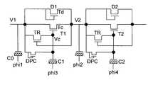
- FIG. 3is a schematic of a charge pump in accordance with one embodiment of the invention in which the cells of the conventional Dickson charge pump are modified to facilitate charge transfer and to accommodate a higher clock frequency or f osc .
- FIG. 3shows two adjacent cells, such as diodes D 1 and D 2 of the Dickson charge pump of FIG. 1 , for transferring charge from node V 1 to node V 2 .
- Each cellis modified by providing a MOS transistor T 1 or T 2 in parallel with diode D 1 or diode D 2 which facilitate the transfer of residual trapped charge at each node.
- a recovery transistor TRis connected between the gate of transistor T 1 and node V 1 with the gate of transistor TR controlled by the voltage on node V 2 .
- FIG. 4illustrates the four phase clock operation of the charge pump of FIG. 3 .
- Charge transfer from node V 1 to node V 2must occur during clock cycle ⁇ 1 when charge coupled through capacitor C 0 raises the charge of node V 1 and forward biases diode D 1 which partially transfers the charge to node V 2 .
- Transistor T 1is in parallel with diode D 1 and conducts in response to clock ⁇ 3 which is shorter than clock ⁇ 1 and lies within clock cycle ⁇ 1 .
- clock ⁇ 3pumps node VC high and transistor T 1 conducts fully and transfers the remaining trapped charge at node V 1 to node V 2 , with node V 1 and node V 2 equalized. This operation is repeated for diode D 2 and transistor T 2 when clock ⁇ 2 is high for stage 2 .
- a pre-charge diode DPCis connected between node V 1 and the gate of transistor T 1 to apply V 1 minus V t on the gate of transistor T 1 before charge transfer. Then, any rise of clock ⁇ 3 will cause the immediate conduction of transistor T 1 and accelerate the transfer of residual charge through transistor T 1 .
- the pre-charge diodeguarantees pre-charge of gate T 1 , the parallel transistor, without the need for clock phase overlap.
- gate of T 1is returned to pre-charge level, which could be slightly higher (initial ramp up phase) or lower (after initial ramp up phase) than after V 1 node fully transfers charge to V 2 , and T 1 could be slightly on or off.
- V 2is coupled high and V 1 is coupled low, and if it is 50/50 transition, the gate of T 1 is a very low capacitive node compared with that of V 1 , V 2 nodes.
- the gate of TRis at V 2 voltage, which is much higher than gate of T 1 , and the charge on gate of T 1 can be quickly discharged. Even if T 1 could be slightly turned on during the recovery phase, since its gate is discharged to source quickly, it is in weak conduction state, the amount of charge that could potentially leak backward from V 2 to V 1 is a very small percentage of charge transferred. If the recovery phase and clock phases are overlapped, it is more like normal four phase charge pump recovery. By using 50/50 clock phases in recovery, no overlap of clocks is required, the clock can run at faster frequencies and the gain of high frequency is much more significant when compared with any potential loss of charge by leakage during recovery transition.
- turn on and turn off of transistor T 1is facilitated by the guaranteed pre-charge of the gate of transistor T 1 to the voltage on node V 1 minus V t prior to turn on, and the equalizing of voltage at the gate of transistor T 1 and the voltage at V 1 in recovery.
- This guaranteed pre-charging and recoverypermits maximum charge transfer forward and minimum charge leakage backward.
- the charge pumpcan operate with 50% cross over of clocks, or overlap of overlap clocks ⁇ 1 and ⁇ 2 , which is unlike prior art four phase charge pumps which require ⁇ 1 and ⁇ 2 overlap to do both pre-charge and discharge of gate equivalent T 1 transistor.
- the charge pump in accordance with the inventionpermits greater efficiency in charge transfer with the same size capacitors as in the prior art Dickson charge pump.
Landscapes
- Engineering & Computer Science (AREA)
- Power Engineering (AREA)
- Dc-Dc Converters (AREA)
Abstract
Description
- This invention relates generally to electric circuits that generate a voltage larger than a supply voltage from which they operate by the switching of charge along serial capacitive cells, known as charge pumps.
- A well known charge pump is the Dickson charge pump, which is shown in
FIG. 1 . As described by Louie Pylarinos of the University of Toronto in “Charge Pumps: An Overview”, the circuit has two pumping clocks which are anti-phased and have a voltage amplitude of Vφ or {overscore (Vφ)}. Serial diodes or diode connected NMOSFETS, D1-D4, operate as self-timed switches characterized by a forward biased voltage, Vt, which is the threshold voltage of each diode. Each diode has a stray capacitance, Cs, associated therewith. The charge pump operates by pumping charge along the diode chain as capacitors C1-C4 are successively charged and discharged during each clock cycle. For example, when Vφ goes high, diode D1 conducts and the voltage at its anode, V1, is boosted by voltage Vφ and transferred to node V2 less a voltage drop, Vt, associated with diode D1. Then when Vφ goes low, and {overscore (Vφ)} goes high, the charge at node V2 is transferred to node V3 less a voltage drop, Vt, associated with diode V2. After N stages, it is seen that the output voltage is
Vout=Vin+N·(Vφ−Vd)−Vd (1)
The stray capacitance, Cs, can be taken into account by noticing that it reduces the transferred clock voltage, Vφ, by a factor
Thus, the actual output voltage becomes - Until now is has been assumed that no load was connected to the output of the charge pump. In the presence of such a load which draws a current, lout, the output voltage is reduced by an amount
where fosc is the operating frequency of the charge pump. The output voltage now becomes
From this equation it becomes apparent that the voltage multiplication will occur only if
Following Dickson, eq (3) can be written as
Equation (3) leads to an equivalent circuit of the charge pump as shown inFIG. 2 . - Limitations of the Dickson charge pump when implemented with NMOS transistors or diode connected transistors lies in the trapped charge associated with each node due to the threshold voltage, Vt, of each NMOS diode. While increasing capacitor charge reduces effective series resistance, Rs, there is a practical limitation of capacitor size in an integrated circuit. While clock frequency, fosc, reduces series resistance, the charge must be able to be transferred from node to node within a cycle, otherwise increasing frequency will not improve pump performance.
- A more efficient charge pump is provided by altering the Dickson charge pump in accordance with the present invention.
- To facilitate charge transfer from one node to the next node, a parallel transistor is provided with each transfer diode whereby residual trapped charge of each node is transferred by the transistor. This requires a transistor clock within each cycle of the diode clock.
- Clock frequency can be increased by providing with each parallel transistor a pre-charge diode to pre-charge the gate of the parallel transistor after the input node is charge is raised but before the charge transfer. This facilitates the conductance of the transistor with each transistor cycle.
- During pre-charge, the pre-charge diode guarantees pre-charge of gate T1, the parallel transistor, without the need for clock phase overlap. A recovery transistor couples the gate of the parallel transistor to the input node to return transistor bias voltage to source voltage in the recovery period where the input node again goes low and the output node is high. Unlike known four phase charge pumps which require overlap of the pumping clocks, the charge pump in accordance with the invention can operate with 50/50 clock pulses having no overlap.
- The invention and objects and features thereof will be more readily apparent from the following detailed description and appended claims when taken with the drawings.
FIG. 1 illustrates a prior art Dickson charge pump.FIG. 2 illustrates an equivalent circuit of the Dickson charge pump.FIG. 3 is a schematic of a charge pump in accordance with one embodiment of the invention.FIG. 4 illustrates clocks for operating the charge pump ofFIG. 3 .FIG. 3 is a schematic of a charge pump in accordance with one embodiment of the invention in which the cells of the conventional Dickson charge pump are modified to facilitate charge transfer and to accommodate a higher clock frequency or fosc.FIG. 3 shows two adjacent cells, such as diodes D1 and D2 of the Dickson charge pump ofFIG. 1 , for transferring charge from node V1 to node V2. Each cell is modified by providing a MOS transistor T1 or T2 in parallel with diode D1 or diode D2 which facilitate the transfer of residual trapped charge at each node. A recovery transistor TR is connected between the gate of transistor T1 and node V1 with the gate of transistor TR controlled by the voltage on node V2. When charge is transferred from node V1 to node V2, the increased voltage at node V2 causes transistor TR to conduct and bring the voltage on the gate of transistor T1 to the voltage level of node V1. After clock φ3 is removed, the conductance of transistor T1 is terminated.FIG. 4 illustrates the four phase clock operation of the charge pump ofFIG. 3 . Charge transfer from node V1 to node V2 must occur during clock cycle φ1 when charge coupled through capacitor C0 raises the charge of node V1 and forward biases diode D1 which partially transfers the charge to node V2.- Transistor T1 is in parallel with diode D1 and conducts in response to clock φ3 which is shorter than clock φ1 and lies within clock cycle φ1. Thus, when φ1 goes high, diode D1 conducts but the current is limited because of the high Vtof the diode. After a short delay, to allow pre-charge from V1 to the gate of T1, clock φ3 pumps node VC high and transistor T1 conducts fully and transfers the remaining trapped charge at node V1 to node V2, with node V1 and node V2 equalized. This operation is repeated for diode D2 and transistor T2 when clock φ2 is high for stage2.
- After charge is transferred from node V1 to node V2 in the first half cycle (Phi1=1, Phi2=0, Phi3=1, Phi4=0), Phi3 goes from 1 to 0 bring down the gate of T1 back to the pre-charge level before charge is transferred. T1 is weakly on at this point or T1 could be completely off depending upon pump operations. In the second half cycle (Phi11=0, Phi12=1), V2 is coupled up by Phi2, V1 is coupled down by Phi11, transistor TR is turned on (V2−V1−Vt>0) and brings the voltage on the gate of transistor T1 to the voltage level of node V1. Since the voltages of T1 gate and source are the same, T1 is completely shut off to prevent any backward leakage.
- To facilitate the conductance of transistor T1 in response to clock φ3, a pre-charge diode DPC is connected between node V1 and the gate of transistor T1 to apply V1 minus Vton the gate of transistor T1 before charge transfer. Then, any rise of clock φ3 will cause the immediate conduction of transistor T1 and accelerate the transfer of residual charge through transistor T1.
- During pre-charge, the pre-charge diode guarantees pre-charge of gate T1, the parallel transistor, without the need for clock phase overlap. Before recovery, since Phi3 goes low before Phi1/Phi2 clocks switch, gate of T1 is returned to pre-charge level, which could be slightly higher (initial ramp up phase) or lower (after initial ramp up phase) than after V1 node fully transfers charge to V2, and T1 could be slightly on or off. In recovery phase, V2 is coupled high and V1 is coupled low, and if it is 50/50 transition, the gate of T1 is a very low capacitive node compared with that of V1, V2 nodes. The gate of TR is at V2 voltage, which is much higher than gate of T1, and the charge on gate of T1 can be quickly discharged. Even if T1 could be slightly turned on during the recovery phase, since its gate is discharged to source quickly, it is in weak conduction state, the amount of charge that could potentially leak backward from V2 to V1 is a very small percentage of charge transferred. If the recovery phase and clock phases are overlapped, it is more like normal four phase charge pump recovery. By using 50/50 clock phases in recovery, no overlap of clocks is required, the clock can run at faster frequencies and the gain of high frequency is much more significant when compared with any potential loss of charge by leakage during recovery transition.
- As noted above, turn on and turn off of transistor T1 is facilitated by the guaranteed pre-charge of the gate of transistor T1 to the voltage on node V1 minus Vtprior to turn on, and the equalizing of voltage at the gate of transistor T1 and the voltage at V1 in recovery. This guaranteed pre-charging and recovery permits maximum charge transfer forward and minimum charge leakage backward. Moreover, the charge pump can operate with 50% cross over of clocks, or overlap of overlap clocks φ1 and φ2, which is unlike prior art four phase charge pumps which require φ1 and φ2 overlap to do both pre-charge and discharge of gate equivalent T1 transistor. Because charge can be fully transferred by boosted T1 transistor, without Vtdrop, capacitance can be reduced per stage to have the same efficiency since no Vtdrops. The equivalent resistance of T1 is much smaller due to boosted gate voltage, and the RC delay per stage to fully transfer charge is much smaller compared with the normal Dickson charge pump. Clock frequency can be in creased due to the smaller RC delay, and faster clock frequency can allow even smaller capacitance per stage to be used to meet the same performance. Accordingly, the charge pump in accordance with the invention permits greater efficiency in charge transfer with the same size capacitors as in the prior art Dickson charge pump.
- While the invention has been described with reference to a specific embodiment, the description is illustrative of the invention, and is not to be construed limiting the invention. Various modifications and applications may occur to those skilled in the art without departing from the true spirit and scope of the invention as defined by the appended claims.
Claims (13)
1. A charge pump comprising a plurality of serially connected cells for pumping and transferring charge along a series of nodes between the cells, each cell including:
a) a charge transfer diode connected between adjacent nodes and responsive to an increasing charge at one node in response to a first clock, φ1, or a second anti-phase second clock, φ2, and
b) a charge transfer transistor connected between the adjacent nodes in parallel with the charge transfer diode and responsive to a third clock, φ3, within the period of clock φ1 or to a fourth clock φ4 within the period of clock φ2,
whereby each charge transfer diode transfers charge from one node to a next node in response to a clock (φ1 or φ2) and each charge transfer transistor transfers residual trapped charge at the one node to the next node while the charge transfer diode is conducting charge.
2. The charge pump as defined byclaim 1 wherein each cell further includes a pre charge diode coupling an input node to a control terminal of the charge transfer transistor to facilitate the conductance of the charge transfer transistor in response to the third clock (φ3) or the fourth clock (φ4).
3. The charge pump as defined byclaim 2 wherein each cell further includes a recovery transistor for equalizing charge on the control terminal of the charge transfer transistor to charge on the input node during a recovery period.
4. The charge pump as defined byclaim 3 wherein each diode comprises a diode NMOSFET and each charge transfer transistor comprises a NMOSFET.
5. The charge pump as defined byclaim 1 wherein each cell further includes a recovery transistor for equalizing charge on the control terminal of the charge transfer transistor to charge on the input node during a recovery period.
6. The charge pump as defined byclaim 5 wherein each diode comprises a diode connected NMOSFET and each charge transfer transistor comprises a NMOSFET.
7. The charge pump as defined byclaim 1 wherein each diode comprises a diode connect NMOSFET and each charge transfer transistor comprises a NMOSFET.
8. A method of increasing efficiency in charge transfer in a charge pump having a plurality of serially connected diodes which sequentially respond to anti-phase pumping clocks (φ1, φ2) comprising the steps of:
a) providing for each diode a charge transfer transistor in parallel therewith between two adjacent nodes, and
b) driving the charge transfer transistor to conduction during a time when the parallel diode is conducting, thereby transferring any residual trapped charge at one node through the charge transfer transistor to the next node.
9. The method as defined byclaim 8 and further including the step of:
c) precharging a control terminal of the charge transfer transistor to facilitate the conductance of the charge transfer transistor.
10. The method as defined byclaim 9 and further including the step of:
d) coupling the control terminal of the charge transfer transistor to an input node in response to charge on an output node to thereby equalize charge on the control terminal and on the input node during a recovery period.
11. The method as defined byclaim 10 wherein each diode comprises a diode connected NMOSFET and each charge transfer transistor comprises a NMOSFET.
12. The method as defined byclaim 8 and further including the step of:
c) coupling the control terminal of the charge transfer transistor to an input node in response to charge on an output node to thereby equalize charge on the control terminal and on the input node during a recovery period.
13. The method as defined byclaim 8 wherein each diode comprises a diode connected NMOSFET and each charge transfer transistor comprises a NMOSFET.
Priority Applications (3)
| Application Number | Priority Date | Filing Date | Title |
|---|---|---|---|
| US10/842,910US7030683B2 (en) | 2004-05-10 | 2004-05-10 | Four phase charge pump operable without phase overlap with improved efficiency |
| PCT/US2005/015762WO2005111757A1 (en) | 2004-05-10 | 2005-05-05 | Four phase charge pump operable without phase overlap with improved efficiency |
| TW094115100ATWI341446B (en) | 2004-05-10 | 2005-05-10 | Charge pump and method of increasing efficiency in charge transfer in a charge pump |
Applications Claiming Priority (1)
| Application Number | Priority Date | Filing Date | Title |
|---|---|---|---|
| US10/842,910US7030683B2 (en) | 2004-05-10 | 2004-05-10 | Four phase charge pump operable without phase overlap with improved efficiency |
Publications (2)
| Publication Number | Publication Date |
|---|---|
| US20050248386A1true US20050248386A1 (en) | 2005-11-10 |
| US7030683B2 US7030683B2 (en) | 2006-04-18 |
Family
ID=35238922
Family Applications (1)
| Application Number | Title | Priority Date | Filing Date |
|---|---|---|---|
| US10/842,910Expired - LifetimeUS7030683B2 (en) | 2004-05-10 | 2004-05-10 | Four phase charge pump operable without phase overlap with improved efficiency |
Country Status (3)
| Country | Link |
|---|---|
| US (1) | US7030683B2 (en) |
| TW (1) | TWI341446B (en) |
| WO (1) | WO2005111757A1 (en) |
Cited By (39)
| Publication number | Priority date | Publication date | Assignee | Title |
|---|---|---|---|---|
| US20080157852A1 (en)* | 2006-12-29 | 2008-07-03 | Sandisk Corporation | Unified voltage generation apparatus with improved power efficiency |
| US20080239836A1 (en)* | 2007-03-30 | 2008-10-02 | Tyler Thorp | Method for Managing Electrical Load of an Electronic Device |
| US20080239801A1 (en)* | 2007-03-30 | 2008-10-02 | Tyler Thorp | Load Management for Memory Device |
| US20080239802A1 (en)* | 2007-03-30 | 2008-10-02 | Tyler Thorp | Device with Load-Based Voltage Generation |
| US20080239856A1 (en)* | 2007-03-30 | 2008-10-02 | Tyler Thorp | Method for Load-Based Voltage Generation |
| US7440342B2 (en) | 2006-12-29 | 2008-10-21 | Sandisk Corporation | Unified voltage generation method with improved power efficiency |
| US20090153231A1 (en)* | 2007-12-12 | 2009-06-18 | Feng Pan | Diode Connected Regulation of Charge Pumps |
| US20090153230A1 (en)* | 2007-12-12 | 2009-06-18 | Feng Pan | Low Voltage Charge Pump with Regulation |
| US20090302930A1 (en)* | 2008-06-09 | 2009-12-10 | Feng Pan | Charge Pump with Vt Cancellation Through Parallel Structure |
| US7683700B2 (en) | 2008-06-25 | 2010-03-23 | Sandisk Corporation | Techniques of ripple reduction for charge pumps |
| US7795952B2 (en) | 2008-12-17 | 2010-09-14 | Sandisk Corporation | Regulation of recovery rates in charge pumps |
| US7969235B2 (en) | 2008-06-09 | 2011-06-28 | Sandisk Corporation | Self-adaptive multi-stage charge pump |
| US7973592B2 (en) | 2009-07-21 | 2011-07-05 | Sandisk Corporation | Charge pump with current based regulation |
| US8044705B2 (en) | 2007-08-28 | 2011-10-25 | Sandisk Technologies Inc. | Bottom plate regulation of charge pumps |
| CN102624222A (en)* | 2012-03-27 | 2012-08-01 | 上海宏力半导体制造有限公司 | Charge pump and charge pump system |
| US8294509B2 (en) | 2010-12-20 | 2012-10-23 | Sandisk Technologies Inc. | Charge pump systems with reduction in inefficiencies due to charge sharing between capacitances |
| US8339183B2 (en) | 2009-07-24 | 2012-12-25 | Sandisk Technologies Inc. | Charge pump with reduced energy consumption through charge sharing and clock boosting suitable for high voltage word line in flash memories |
| US8339185B2 (en) | 2010-12-20 | 2012-12-25 | Sandisk 3D Llc | Charge pump system that dynamically selects number of active stages |
| US8400212B1 (en) | 2011-09-22 | 2013-03-19 | Sandisk Technologies Inc. | High voltage charge pump regulation system with fine step adjustment |
| CN103138566A (en)* | 2011-11-23 | 2013-06-05 | 上海华虹Nec电子有限公司 | Control circuit for various high voltage output by single charge pump |
| US8514628B2 (en) | 2011-09-22 | 2013-08-20 | Sandisk Technologies Inc. | Dynamic switching approach to reduce area and power consumption of high voltage charge pumps |
| TWI413127B (en)* | 2007-11-26 | 2013-10-21 | Elite Semiconductor Esmt | Charge pump circuit and cell thereof |
| US8699247B2 (en) | 2011-09-09 | 2014-04-15 | Sandisk Technologies Inc. | Charge pump system dynamically reconfigurable for read and program |
| US8710907B2 (en) | 2008-06-24 | 2014-04-29 | Sandisk Technologies Inc. | Clock generator circuit for a charge pump |
| US8710909B2 (en) | 2012-09-14 | 2014-04-29 | Sandisk Technologies Inc. | Circuits for prevention of reverse leakage in Vth-cancellation charge pumps |
| US8836412B2 (en) | 2013-02-11 | 2014-09-16 | Sandisk 3D Llc | Charge pump with a power-controlled clock buffer to reduce power consumption and output voltage ripple |
| US8981835B2 (en) | 2013-06-18 | 2015-03-17 | Sandisk Technologies Inc. | Efficient voltage doubler |
| US9007046B2 (en) | 2013-06-27 | 2015-04-14 | Sandisk Technologies Inc. | Efficient high voltage bias regulation circuit |
| US9024680B2 (en) | 2013-06-24 | 2015-05-05 | Sandisk Technologies Inc. | Efficiency for charge pumps with low supply voltages |
| US9077238B2 (en) | 2013-06-25 | 2015-07-07 | SanDisk Technologies, Inc. | Capacitive regulation of charge pumps without refresh operation interruption |
| CN104767383A (en)* | 2015-04-21 | 2015-07-08 | 苏州芯宽电子科技有限公司 | Low-voltage four-phase charge pump boosted circuit |
| US9083231B2 (en) | 2013-09-30 | 2015-07-14 | Sandisk Technologies Inc. | Amplitude modulation for pass gate to improve charge pump efficiency |
| US9154027B2 (en) | 2013-12-09 | 2015-10-06 | Sandisk Technologies Inc. | Dynamic load matching charge pump for reduced current consumption |
| CN105336368A (en)* | 2014-07-18 | 2016-02-17 | 北京兆易创新科技股份有限公司 | Non-overlapping four-phase clock generation circuit |
| US9520776B1 (en) | 2015-09-18 | 2016-12-13 | Sandisk Technologies Llc | Selective body bias for charge pump transfer switches |
| US9647536B2 (en) | 2015-07-28 | 2017-05-09 | Sandisk Technologies Llc | High voltage generation using low voltage devices |
| US9917507B2 (en) | 2015-05-28 | 2018-03-13 | Sandisk Technologies Llc | Dynamic clock period modulation scheme for variable charge pump load currents |
| US10847227B2 (en) | 2018-10-16 | 2020-11-24 | Silicon Storage Technology, Inc. | Charge pump for use in non-volatile flash memory devices |
| WO2020256555A1 (en)* | 2019-06-21 | 2020-12-24 | Nowi Energy B.V. | Dc-dc converter |
Families Citing this family (47)
| Publication number | Priority date | Publication date | Assignee | Title |
|---|---|---|---|---|
| JP2006311703A (en)* | 2005-04-28 | 2006-11-09 | Seiko Instruments Inc | Electronic apparatus having charge pump circuit |
| WO2007149559A2 (en)* | 2006-06-22 | 2007-12-27 | Board Of Regents Of The University Of Nebraska | Magnetically coupleable robotic devices and related methods |
| JP4284345B2 (en)* | 2006-08-30 | 2009-06-24 | 株式会社 日立ディスプレイズ | Voltage conversion circuit and display device including the voltage conversion circuit |
| JP2008092667A (en)* | 2006-10-02 | 2008-04-17 | Seiko Instruments Inc | Electronic equipment with step-up circuit |
| US7741898B2 (en)* | 2007-01-23 | 2010-06-22 | Etron Technology, Inc. | Charge pump circuit for high voltage generation |
| KR100877623B1 (en)* | 2007-02-12 | 2009-01-09 | 삼성전자주식회사 | High voltage generation circuit and its method for reducing peak current and power supply noise |
| TWI328925B (en)* | 2007-04-11 | 2010-08-11 | Au Optronics Corp | Negative voltage converter |
| US7446596B1 (en)* | 2007-05-25 | 2008-11-04 | Atmel Corporation | Low voltage charge pump |
| US20090058507A1 (en)* | 2007-08-28 | 2009-03-05 | Prajit Nandi | Bottom Plate Regulated Charge Pump |
| TW200945751A (en)* | 2008-04-17 | 2009-11-01 | Sitronix Technology Corp | Charge pump |
| WO2011013403A1 (en)* | 2009-07-29 | 2011-02-03 | 京セラ株式会社 | Transfer gate circuit, and power combining circuit, power amplifying circuit, transmission device, and communication device using the transfer gate circuit |
| US20110133820A1 (en)* | 2009-12-09 | 2011-06-09 | Feng Pan | Multi-Stage Charge Pump with Variable Number of Boosting Stages |
| US20110148509A1 (en) | 2009-12-17 | 2011-06-23 | Feng Pan | Techniques to Reduce Charge Pump Overshoot |
| US8432732B2 (en) | 2010-07-09 | 2013-04-30 | Sandisk Technologies Inc. | Detection of word-line leakage in memory arrays |
| US8514630B2 (en) | 2010-07-09 | 2013-08-20 | Sandisk Technologies Inc. | Detection of word-line leakage in memory arrays: current based approach |
| US8305807B2 (en) | 2010-07-09 | 2012-11-06 | Sandisk Technologies Inc. | Detection of broken word-lines in memory arrays |
| US8106701B1 (en) | 2010-09-30 | 2012-01-31 | Sandisk Technologies Inc. | Level shifter with shoot-through current isolation |
| US8274322B2 (en)* | 2010-10-18 | 2012-09-25 | National Tsing Hua University | Charge pump with low noise and high output current and voltage |
| US8537593B2 (en) | 2011-04-28 | 2013-09-17 | Sandisk Technologies Inc. | Variable resistance switch suitable for supplying high voltage to drive load |
| US8379454B2 (en) | 2011-05-05 | 2013-02-19 | Sandisk Technologies Inc. | Detection of broken word-lines in memory arrays |
| US8775901B2 (en) | 2011-07-28 | 2014-07-08 | SanDisk Technologies, Inc. | Data recovery for defective word lines during programming of non-volatile memory arrays |
| US8726104B2 (en) | 2011-07-28 | 2014-05-13 | Sandisk Technologies Inc. | Non-volatile memory and method with accelerated post-write read using combined verification of multiple pages |
| US8750042B2 (en) | 2011-07-28 | 2014-06-10 | Sandisk Technologies Inc. | Combined simultaneous sensing of multiple wordlines in a post-write read (PWR) and detection of NAND failures |
| US8395434B1 (en) | 2011-10-05 | 2013-03-12 | Sandisk Technologies Inc. | Level shifter with negative voltage capability |
| TWI496143B (en)* | 2011-10-18 | 2015-08-11 | Winbond Electronics Corp | Voltage generator |
| US8928395B2 (en)* | 2012-01-17 | 2015-01-06 | Winbond Electronics Corp. | Voltage generator |
| US8730722B2 (en) | 2012-03-02 | 2014-05-20 | Sandisk Technologies Inc. | Saving of data in cases of word-line to word-line short in memory arrays |
| US9810723B2 (en) | 2012-09-27 | 2017-11-07 | Sandisk Technologies Llc | Charge pump based over-sampling ADC for current detection |
| US9164526B2 (en) | 2012-09-27 | 2015-10-20 | Sandisk Technologies Inc. | Sigma delta over-sampling charge pump analog-to-digital converter |
| KR20150087410A (en)* | 2012-12-19 | 2015-07-29 | 노우레스 일렉트로닉스, 엘엘시 | Apparatus and method for high voltage I/O electro-static discharge protection |
| US9165683B2 (en) | 2013-09-23 | 2015-10-20 | Sandisk Technologies Inc. | Multi-word line erratic programming detection |
| US20160006348A1 (en)* | 2014-07-07 | 2016-01-07 | Ememory Technology Inc. | Charge pump apparatus |
| US9460809B2 (en) | 2014-07-10 | 2016-10-04 | Sandisk Technologies Llc | AC stress mode to screen out word line to word line shorts |
| US9514835B2 (en) | 2014-07-10 | 2016-12-06 | Sandisk Technologies Llc | Determination of word line to word line shorts between adjacent blocks |
| US9484086B2 (en) | 2014-07-10 | 2016-11-01 | Sandisk Technologies Llc | Determination of word line to local source line shorts |
| US9443612B2 (en) | 2014-07-10 | 2016-09-13 | Sandisk Technologies Llc | Determination of bit line to low voltage signal shorts |
| US9330776B2 (en) | 2014-08-14 | 2016-05-03 | Sandisk Technologies Inc. | High voltage step down regulator with breakdown protection |
| US9202593B1 (en) | 2014-09-02 | 2015-12-01 | Sandisk Technologies Inc. | Techniques for detecting broken word lines in non-volatile memories |
| US9240249B1 (en) | 2014-09-02 | 2016-01-19 | Sandisk Technologies Inc. | AC stress methods to screen out bit line defects |
| US9449694B2 (en) | 2014-09-04 | 2016-09-20 | Sandisk Technologies Llc | Non-volatile memory with multi-word line select for defect detection operations |
| US9659666B2 (en) | 2015-08-31 | 2017-05-23 | Sandisk Technologies Llc | Dynamic memory recovery at the sub-block level |
| US9698676B1 (en) | 2016-03-11 | 2017-07-04 | Sandisk Technologies Llc | Charge pump based over-sampling with uniform step size for current detection |
| US9917510B2 (en)* | 2016-07-21 | 2018-03-13 | Dialog Semiconductor (Uk) Limited | Multi-staged buck converter with efficient low power operation |
| US10461635B1 (en) | 2018-05-15 | 2019-10-29 | Analog Devices Global Unlimited Company | Low VIN high efficiency chargepump |
| US10707749B2 (en)* | 2018-07-31 | 2020-07-07 | Samsung Electronics Co., Ltd. | Charge pump, and high voltage generator and flash memory device having the same |
| US11908521B2 (en) | 2022-02-01 | 2024-02-20 | Western Digital Technologies, Inc. | Non-volatile memory with redundant control line driver |
| US12348132B2 (en) | 2023-02-16 | 2025-07-01 | SanDisk Technologies, Inc. | Stage based frequency optimization for area reduction of charge pumps |
Citations (9)
| Publication number | Priority date | Publication date | Assignee | Title |
|---|---|---|---|---|
| US5754476A (en)* | 1995-10-31 | 1998-05-19 | Sgs-Thomson Microelectronics S.R.L. | Negative charge pump circuit for electrically erasable semiconductor memory devices |
| US6175264B1 (en)* | 1998-03-16 | 2001-01-16 | Nec Corporation | Charge pump for generating negative voltage without change of threshold due to undesirable back-gate biasing effect |
| US6292048B1 (en)* | 1999-11-11 | 2001-09-18 | Intel Corporation | Gate enhancement charge pump for low voltage power supply |
| US6373324B2 (en)* | 1998-08-21 | 2002-04-16 | Intel Corporation | Voltage blocking method and apparatus for a charge pump with diode connected pull-up and pull-down on boot nodes |
| US6452438B1 (en)* | 2000-12-28 | 2002-09-17 | Intel Corporation | Triple well no body effect negative charge pump |
| US20030214346A1 (en)* | 2002-02-25 | 2003-11-20 | Stmicroelectronics S.R.I. | Charge pump for negative voltages |
| US6690227B2 (en)* | 2001-07-07 | 2004-02-10 | Samsung Electronics Co., Ltd. | Charge pump circuit for use in high voltage generating circuit |
| US20050088220A1 (en)* | 2003-10-27 | 2005-04-28 | Hahn Wook-Ghee | Charge pump circuit having high charge transfer efficiency |
| US20050146375A1 (en)* | 2004-01-02 | 2005-07-07 | Ming-Dou Ker | Charge pump circuit suitable for low-voltage process |
- 2004
- 2004-05-10USUS10/842,910patent/US7030683B2/ennot_activeExpired - Lifetime
- 2005
- 2005-05-05WOPCT/US2005/015762patent/WO2005111757A1/enactiveApplication Filing
- 2005-05-10TWTW094115100Apatent/TWI341446B/ennot_activeIP Right Cessation
Patent Citations (9)
| Publication number | Priority date | Publication date | Assignee | Title |
|---|---|---|---|---|
| US5754476A (en)* | 1995-10-31 | 1998-05-19 | Sgs-Thomson Microelectronics S.R.L. | Negative charge pump circuit for electrically erasable semiconductor memory devices |
| US6175264B1 (en)* | 1998-03-16 | 2001-01-16 | Nec Corporation | Charge pump for generating negative voltage without change of threshold due to undesirable back-gate biasing effect |
| US6373324B2 (en)* | 1998-08-21 | 2002-04-16 | Intel Corporation | Voltage blocking method and apparatus for a charge pump with diode connected pull-up and pull-down on boot nodes |
| US6292048B1 (en)* | 1999-11-11 | 2001-09-18 | Intel Corporation | Gate enhancement charge pump for low voltage power supply |
| US6452438B1 (en)* | 2000-12-28 | 2002-09-17 | Intel Corporation | Triple well no body effect negative charge pump |
| US6690227B2 (en)* | 2001-07-07 | 2004-02-10 | Samsung Electronics Co., Ltd. | Charge pump circuit for use in high voltage generating circuit |
| US20030214346A1 (en)* | 2002-02-25 | 2003-11-20 | Stmicroelectronics S.R.I. | Charge pump for negative voltages |
| US20050088220A1 (en)* | 2003-10-27 | 2005-04-28 | Hahn Wook-Ghee | Charge pump circuit having high charge transfer efficiency |
| US20050146375A1 (en)* | 2004-01-02 | 2005-07-07 | Ming-Dou Ker | Charge pump circuit suitable for low-voltage process |
Cited By (58)
| Publication number | Priority date | Publication date | Assignee | Title |
|---|---|---|---|---|
| US7440342B2 (en) | 2006-12-29 | 2008-10-21 | Sandisk Corporation | Unified voltage generation method with improved power efficiency |
| US7477092B2 (en) | 2006-12-29 | 2009-01-13 | Sandisk Corporation | Unified voltage generation apparatus with improved power efficiency |
| US20080157852A1 (en)* | 2006-12-29 | 2008-07-03 | Sandisk Corporation | Unified voltage generation apparatus with improved power efficiency |
| US7558129B2 (en) | 2007-03-30 | 2009-07-07 | Sandisk 3D Llc | Device with load-based voltage generation |
| US20080239836A1 (en)* | 2007-03-30 | 2008-10-02 | Tyler Thorp | Method for Managing Electrical Load of an Electronic Device |
| US20080239801A1 (en)* | 2007-03-30 | 2008-10-02 | Tyler Thorp | Load Management for Memory Device |
| US20080239802A1 (en)* | 2007-03-30 | 2008-10-02 | Tyler Thorp | Device with Load-Based Voltage Generation |
| US20080239856A1 (en)* | 2007-03-30 | 2008-10-02 | Tyler Thorp | Method for Load-Based Voltage Generation |
| US7515488B2 (en) | 2007-03-30 | 2009-04-07 | Sandisk 3D Llc | Method for load-based voltage generation |
| US7580298B2 (en) | 2007-03-30 | 2009-08-25 | Sandisk 3D Llc | Method for managing electrical load of an electronic device |
| US7580296B2 (en) | 2007-03-30 | 2009-08-25 | Sandisk 3D Llc | Load management for memory device |
| US8044705B2 (en) | 2007-08-28 | 2011-10-25 | Sandisk Technologies Inc. | Bottom plate regulation of charge pumps |
| TWI413127B (en)* | 2007-11-26 | 2013-10-21 | Elite Semiconductor Esmt | Charge pump circuit and cell thereof |
| WO2009076137A1 (en)* | 2007-12-12 | 2009-06-18 | Sandisk Corporation | Diode connected regulation of charge pumps |
| US7586363B2 (en) | 2007-12-12 | 2009-09-08 | Sandisk Corporation | Diode connected regulation of charge pumps |
| US7586362B2 (en) | 2007-12-12 | 2009-09-08 | Sandisk Corporation | Low voltage charge pump with regulation |
| US20090153230A1 (en)* | 2007-12-12 | 2009-06-18 | Feng Pan | Low Voltage Charge Pump with Regulation |
| US20090153231A1 (en)* | 2007-12-12 | 2009-06-18 | Feng Pan | Diode Connected Regulation of Charge Pumps |
| US20090302930A1 (en)* | 2008-06-09 | 2009-12-10 | Feng Pan | Charge Pump with Vt Cancellation Through Parallel Structure |
| US7969235B2 (en) | 2008-06-09 | 2011-06-28 | Sandisk Corporation | Self-adaptive multi-stage charge pump |
| US8710907B2 (en) | 2008-06-24 | 2014-04-29 | Sandisk Technologies Inc. | Clock generator circuit for a charge pump |
| US7683700B2 (en) | 2008-06-25 | 2010-03-23 | Sandisk Corporation | Techniques of ripple reduction for charge pumps |
| US7795952B2 (en) | 2008-12-17 | 2010-09-14 | Sandisk Corporation | Regulation of recovery rates in charge pumps |
| US7973592B2 (en) | 2009-07-21 | 2011-07-05 | Sandisk Corporation | Charge pump with current based regulation |
| US8339183B2 (en) | 2009-07-24 | 2012-12-25 | Sandisk Technologies Inc. | Charge pump with reduced energy consumption through charge sharing and clock boosting suitable for high voltage word line in flash memories |
| US8339185B2 (en) | 2010-12-20 | 2012-12-25 | Sandisk 3D Llc | Charge pump system that dynamically selects number of active stages |
| US8294509B2 (en) | 2010-12-20 | 2012-10-23 | Sandisk Technologies Inc. | Charge pump systems with reduction in inefficiencies due to charge sharing between capacitances |
| US8421524B2 (en) | 2010-12-20 | 2013-04-16 | Sandisk Technologies Inc. | Charge pump systems with reduction in inefficiencies due to charge sharing between capacitances |
| USRE46263E1 (en) | 2010-12-20 | 2017-01-03 | Sandisk Technologies Llc | Charge pump system that dynamically selects number of active stages |
| US8699247B2 (en) | 2011-09-09 | 2014-04-15 | Sandisk Technologies Inc. | Charge pump system dynamically reconfigurable for read and program |
| US8514628B2 (en) | 2011-09-22 | 2013-08-20 | Sandisk Technologies Inc. | Dynamic switching approach to reduce area and power consumption of high voltage charge pumps |
| US8400212B1 (en) | 2011-09-22 | 2013-03-19 | Sandisk Technologies Inc. | High voltage charge pump regulation system with fine step adjustment |
| CN103138566A (en)* | 2011-11-23 | 2013-06-05 | 上海华虹Nec电子有限公司 | Control circuit for various high voltage output by single charge pump |
| CN102624222A (en)* | 2012-03-27 | 2012-08-01 | 上海宏力半导体制造有限公司 | Charge pump and charge pump system |
| US8710909B2 (en) | 2012-09-14 | 2014-04-29 | Sandisk Technologies Inc. | Circuits for prevention of reverse leakage in Vth-cancellation charge pumps |
| US8836412B2 (en) | 2013-02-11 | 2014-09-16 | Sandisk 3D Llc | Charge pump with a power-controlled clock buffer to reduce power consumption and output voltage ripple |
| US8860501B2 (en) | 2013-02-11 | 2014-10-14 | Sandisk 3D Llc | Charge pump with a power-controlled clock buffer to reduce power consumption and output voltage ripple |
| US8981835B2 (en) | 2013-06-18 | 2015-03-17 | Sandisk Technologies Inc. | Efficient voltage doubler |
| US9024680B2 (en) | 2013-06-24 | 2015-05-05 | Sandisk Technologies Inc. | Efficiency for charge pumps with low supply voltages |
| US9077238B2 (en) | 2013-06-25 | 2015-07-07 | SanDisk Technologies, Inc. | Capacitive regulation of charge pumps without refresh operation interruption |
| US9007046B2 (en) | 2013-06-27 | 2015-04-14 | Sandisk Technologies Inc. | Efficient high voltage bias regulation circuit |
| US9083231B2 (en) | 2013-09-30 | 2015-07-14 | Sandisk Technologies Inc. | Amplitude modulation for pass gate to improve charge pump efficiency |
| US9154027B2 (en) | 2013-12-09 | 2015-10-06 | Sandisk Technologies Inc. | Dynamic load matching charge pump for reduced current consumption |
| CN105336368A (en)* | 2014-07-18 | 2016-02-17 | 北京兆易创新科技股份有限公司 | Non-overlapping four-phase clock generation circuit |
| CN104767383A (en)* | 2015-04-21 | 2015-07-08 | 苏州芯宽电子科技有限公司 | Low-voltage four-phase charge pump boosted circuit |
| US9917507B2 (en) | 2015-05-28 | 2018-03-13 | Sandisk Technologies Llc | Dynamic clock period modulation scheme for variable charge pump load currents |
| US9647536B2 (en) | 2015-07-28 | 2017-05-09 | Sandisk Technologies Llc | High voltage generation using low voltage devices |
| US9520776B1 (en) | 2015-09-18 | 2016-12-13 | Sandisk Technologies Llc | Selective body bias for charge pump transfer switches |
| TWI716137B (en)* | 2018-10-16 | 2021-01-11 | 美商超捷公司 | Improved charge pump for use in non-volatile flash memory devices |
| US10847227B2 (en) | 2018-10-16 | 2020-11-24 | Silicon Storage Technology, Inc. | Charge pump for use in non-volatile flash memory devices |
| CN112868062A (en)* | 2018-10-16 | 2021-05-28 | 硅存储技术股份有限公司 | Improved charge pump for use in non-volatile flash memory devices |
| US11120881B2 (en) | 2018-10-16 | 2021-09-14 | Silicon Storage Technology, Inc. | Charge pump for use in non-volatile flash memory devices |
| JP2022505083A (en)* | 2018-10-16 | 2022-01-14 | シリコン ストーリッジ テクノロージー インコーポレイテッド | Improved charge pump used in non-volatile flash memory devices |
| EP3867903B1 (en)* | 2018-10-16 | 2023-03-29 | Silicon Storage Technology, Inc. | Improved charge pump for use in non-volatile flash memory devices |
| JP7407809B2 (en) | 2018-10-16 | 2024-01-04 | シリコン ストーリッジ テクノロージー インコーポレイテッド | Improved charge pump used in non-volatile flash memory devices |
| WO2020256555A1 (en)* | 2019-06-21 | 2020-12-24 | Nowi Energy B.V. | Dc-dc converter |
| CN114223123A (en)* | 2019-06-21 | 2022-03-22 | 诺维能源公司 | DC-DC converter |
| US12046994B2 (en) | 2019-06-21 | 2024-07-23 | Nexperia B.V. | DC-DC converter |
Also Published As
| Publication number | Publication date |
|---|---|
| WO2005111757A1 (en) | 2005-11-24 |
| TW200619894A (en) | 2006-06-16 |
| US7030683B2 (en) | 2006-04-18 |
| TWI341446B (en) | 2011-05-01 |
Similar Documents
| Publication | Publication Date | Title |
|---|---|---|
| US7030683B2 (en) | Four phase charge pump operable without phase overlap with improved efficiency | |
| US7113023B2 (en) | Area efficient charge pump | |
| KR100834195B1 (en) | Charge Pump Power Supply | |
| US6661682B2 (en) | High voltage generating charge pump circuit | |
| US6501325B1 (en) | Low voltage supply higher efficiency cross-coupled high voltage charge pumps | |
| US7602233B2 (en) | Voltage multiplier with improved efficiency | |
| EP1899785B1 (en) | Efficient charge pump for a wide range of supply voltages | |
| US5994949A (en) | Negative voltage charge pump particularly for flash EEPROM memories | |
| US20070285150A1 (en) | Method and system for providing a charge pump very low voltage applications | |
| US6356137B1 (en) | Voltage boost circuit with low power supply voltage | |
| WO1998020401A1 (en) | Positive/negative high voltage charge pump system | |
| JPH06261538A (en) | High-voltage charge pump | |
| WO2008030728A2 (en) | High efficiency low cost bi-directional charge pump circuit for very low voltage applications | |
| US7714636B2 (en) | Charge pump circuit and cell thereof | |
| CN100568689C (en) | Charge pump power supply | |
| US6605985B2 (en) | High-efficiency power charge pump supplying high DC output currents | |
| US5543668A (en) | Charge stacking on-chip high-voltage generator and method | |
| EP0865149B1 (en) | High current CMOS charge pump, particularly for flash EEPROM memories | |
| EP0798845A2 (en) | Voltage-boosting circuit with mode signal | |
| US20060120157A1 (en) | Charge-pump device with increased current output | |
| US7688001B2 (en) | Method and system for providing a charge pump for low voltage applications | |
| US7095268B2 (en) | Single-stage and modular multi-stage clock-booster | |
| EP0851562B1 (en) | High voltage charge pump, particularly for flash EEPROM memories | |
| Zhao et al. | Negative high voltage DC-DC converter using a New Cross-coupled Structure | |
| HK1119793A (en) | Efficient charge pump for a wide range of supply voltages |
Legal Events
| Date | Code | Title | Description |
|---|---|---|---|
| AS | Assignment | Owner name:SANDISK CORPORATION, CALIFORNIA Free format text:ASSIGNMENT OF ASSIGNORS INTEREST;ASSIGNORS:PAN, FENG;PHAM, TRUNG;REEL/FRAME:015321/0239 Effective date:20040504 | |
| STCF | Information on status: patent grant | Free format text:PATENTED CASE | |
| FPAY | Fee payment | Year of fee payment:4 | |
| AS | Assignment | Owner name:SANDISK TECHNOLOGIES INC., TEXAS Free format text:ASSIGNMENT OF ASSIGNORS INTEREST;ASSIGNOR:SANDISK CORPORATION;REEL/FRAME:026339/0638 Effective date:20110404 | |
| FPAY | Fee payment | Year of fee payment:8 | |
| AS | Assignment | Owner name:SANDISK TECHNOLOGIES LLC, TEXAS Free format text:CHANGE OF NAME;ASSIGNOR:SANDISK TECHNOLOGIES INC;REEL/FRAME:038813/0004 Effective date:20160516 | |
| MAFP | Maintenance fee payment | Free format text:PAYMENT OF MAINTENANCE FEE, 12TH YEAR, LARGE ENTITY (ORIGINAL EVENT CODE: M1553) Year of fee payment:12 |