US20050245085A1 - Method for forming pattern using printing method - Google Patents
Method for forming pattern using printing methodDownload PDFInfo
- Publication number
- US20050245085A1 US20050245085A1US11/114,095US11409505AUS2005245085A1US 20050245085 A1US20050245085 A1US 20050245085A1US 11409505 AUS11409505 AUS 11409505AUS 2005245085 A1US2005245085 A1US 2005245085A1
- Authority
- US
- United States
- Prior art keywords
- cliché
- substrate
- ink
- patterns
- pattern
- Prior art date
- Legal status (The legal status is an assumption and is not a legal conclusion. Google has not performed a legal analysis and makes no representation as to the accuracy of the status listed.)
- Granted
Links
Images


Classifications
- H—ELECTRICITY
- H01—ELECTRIC ELEMENTS
- H01L—SEMICONDUCTOR DEVICES NOT COVERED BY CLASS H10
- H01L21/00—Processes or apparatus adapted for the manufacture or treatment of semiconductor or solid state devices or of parts thereof
- H01L21/70—Manufacture or treatment of devices consisting of a plurality of solid state components formed in or on a common substrate or of parts thereof; Manufacture of integrated circuit devices or of parts thereof
- H01L21/71—Manufacture of specific parts of devices defined in group H01L21/70
- H01L21/768—Applying interconnections to be used for carrying current between separate components within a device comprising conductors and dielectrics
- H01L21/76838—Applying interconnections to be used for carrying current between separate components within a device comprising conductors and dielectrics characterised by the formation and the after-treatment of the conductors
- G—PHYSICS
- G21—NUCLEAR PHYSICS; NUCLEAR ENGINEERING
- G21F—PROTECTION AGAINST X-RADIATION, GAMMA RADIATION, CORPUSCULAR RADIATION OR PARTICLE BOMBARDMENT; TREATING RADIOACTIVELY CONTAMINATED MATERIAL; DECONTAMINATION ARRANGEMENTS THEREFOR
- G21F3/00—Shielding characterised by its physical form, e.g. granules, or shape of the material
- G21F3/04—Bricks; Shields made up therefrom
- B—PERFORMING OPERATIONS; TRANSPORTING
- B82—NANOTECHNOLOGY
- B82Y—SPECIFIC USES OR APPLICATIONS OF NANOSTRUCTURES; MEASUREMENT OR ANALYSIS OF NANOSTRUCTURES; MANUFACTURE OR TREATMENT OF NANOSTRUCTURES
- B82Y10/00—Nanotechnology for information processing, storage or transmission, e.g. quantum computing or single electron logic
- B—PERFORMING OPERATIONS; TRANSPORTING
- B82—NANOTECHNOLOGY
- B82Y—SPECIFIC USES OR APPLICATIONS OF NANOSTRUCTURES; MEASUREMENT OR ANALYSIS OF NANOSTRUCTURES; MANUFACTURE OR TREATMENT OF NANOSTRUCTURES
- B82Y40/00—Manufacture or treatment of nanostructures
- G—PHYSICS
- G03—PHOTOGRAPHY; CINEMATOGRAPHY; ANALOGOUS TECHNIQUES USING WAVES OTHER THAN OPTICAL WAVES; ELECTROGRAPHY; HOLOGRAPHY
- G03F—PHOTOMECHANICAL PRODUCTION OF TEXTURED OR PATTERNED SURFACES, e.g. FOR PRINTING, FOR PROCESSING OF SEMICONDUCTOR DEVICES; MATERIALS THEREFOR; ORIGINALS THEREFOR; APPARATUS SPECIALLY ADAPTED THEREFOR
- G03F7/00—Photomechanical, e.g. photolithographic, production of textured or patterned surfaces, e.g. printing surfaces; Materials therefor, e.g. comprising photoresists; Apparatus specially adapted therefor
- G03F7/0002—Lithographic processes using patterning methods other than those involving the exposure to radiation, e.g. by stamping
- G—PHYSICS
- G21—NUCLEAR PHYSICS; NUCLEAR ENGINEERING
- G21F—PROTECTION AGAINST X-RADIATION, GAMMA RADIATION, CORPUSCULAR RADIATION OR PARTICLE BOMBARDMENT; TREATING RADIOACTIVELY CONTAMINATED MATERIAL; DECONTAMINATION ARRANGEMENTS THEREFOR
- G21F1/00—Shielding characterised by the composition of the materials
- G21F1/02—Selection of uniform shielding materials
- G21F1/04—Concretes; Other hydraulic hardening materials
- H—ELECTRICITY
- H05—ELECTRIC TECHNIQUES NOT OTHERWISE PROVIDED FOR
- H05K—PRINTED CIRCUITS; CASINGS OR CONSTRUCTIONAL DETAILS OF ELECTRIC APPARATUS; MANUFACTURE OF ASSEMBLAGES OF ELECTRICAL COMPONENTS
- H05K3/00—Apparatus or processes for manufacturing printed circuits
- H05K3/02—Apparatus or processes for manufacturing printed circuits in which the conductive material is applied to the surface of the insulating support and is thereafter removed from such areas of the surface which are not intended for current conducting or shielding
- H05K3/06—Apparatus or processes for manufacturing printed circuits in which the conductive material is applied to the surface of the insulating support and is thereafter removed from such areas of the surface which are not intended for current conducting or shielding the conductive material being removed chemically or electrolytically, e.g. by photo-etch process
- H05K3/061—Etching masks
- G—PHYSICS
- G02—OPTICS
- G02F—OPTICAL DEVICES OR ARRANGEMENTS FOR THE CONTROL OF LIGHT BY MODIFICATION OF THE OPTICAL PROPERTIES OF THE MEDIA OF THE ELEMENTS INVOLVED THEREIN; NON-LINEAR OPTICS; FREQUENCY-CHANGING OF LIGHT; OPTICAL LOGIC ELEMENTS; OPTICAL ANALOGUE/DIGITAL CONVERTERS
- G02F1/00—Devices or arrangements for the control of the intensity, colour, phase, polarisation or direction of light arriving from an independent light source, e.g. switching, gating or modulating; Non-linear optics
- G02F1/01—Devices or arrangements for the control of the intensity, colour, phase, polarisation or direction of light arriving from an independent light source, e.g. switching, gating or modulating; Non-linear optics for the control of the intensity, phase, polarisation or colour
- G02F1/13—Devices or arrangements for the control of the intensity, colour, phase, polarisation or direction of light arriving from an independent light source, e.g. switching, gating or modulating; Non-linear optics for the control of the intensity, phase, polarisation or colour based on liquid crystals, e.g. single liquid crystal display cells
- G02F1/133—Constructional arrangements; Operation of liquid crystal cells; Circuit arrangements
- G02F1/136—Liquid crystal cells structurally associated with a semi-conducting layer or substrate, e.g. cells forming part of an integrated circuit
- G02F1/1362—Active matrix addressed cells
- G02F1/136286—Wiring, e.g. gate line, drain line
- G02F1/136295—Materials; Compositions; Manufacture processes
- H—ELECTRICITY
- H05—ELECTRIC TECHNIQUES NOT OTHERWISE PROVIDED FOR
- H05K—PRINTED CIRCUITS; CASINGS OR CONSTRUCTIONAL DETAILS OF ELECTRIC APPARATUS; MANUFACTURE OF ASSEMBLAGES OF ELECTRICAL COMPONENTS
- H05K2203/00—Indexing scheme relating to apparatus or processes for manufacturing printed circuits covered by H05K3/00
- H05K2203/01—Tools for processing; Objects used during processing
- H05K2203/0104—Tools for processing; Objects used during processing for patterning or coating
- H05K2203/0108—Male die used for patterning, punching or transferring
- H—ELECTRICITY
- H05—ELECTRIC TECHNIQUES NOT OTHERWISE PROVIDED FOR
- H05K—PRINTED CIRCUITS; CASINGS OR CONSTRUCTIONAL DETAILS OF ELECTRIC APPARATUS; MANUFACTURE OF ASSEMBLAGES OF ELECTRICAL COMPONENTS
- H05K2203/00—Indexing scheme relating to apparatus or processes for manufacturing printed circuits covered by H05K3/00
- H05K2203/05—Patterning and lithography; Masks; Details of resist
- H05K2203/0502—Patterning and lithography
- H05K2203/0522—Using an adhesive pattern
- H—ELECTRICITY
- H05—ELECTRIC TECHNIQUES NOT OTHERWISE PROVIDED FOR
- H05K—PRINTED CIRCUITS; CASINGS OR CONSTRUCTIONAL DETAILS OF ELECTRIC APPARATUS; MANUFACTURE OF ASSEMBLAGES OF ELECTRICAL COMPONENTS
- H05K2203/00—Indexing scheme relating to apparatus or processes for manufacturing printed circuits covered by H05K3/00
- H05K2203/05—Patterning and lithography; Masks; Details of resist
- H05K2203/0502—Patterning and lithography
- H05K2203/0537—Transfer of pre-fabricated insulating pattern
Definitions
- the present inventionrelates to a printing method for forming a pattern in a liquid crystal display panel, and more particularly, to a method for forming a pattern with uniform thickness on a substrate.
- a display deviceespecially, a flat panel display such as a liquid crystal display (LCD) device is driven by an active device such as a thin film transistor provided at each pixel.
- the driving methodis referred as an active matrix driving method.
- the active deviceis arranged at each pixel to drive the corresponding pixel.
- FIG. 1is a view illustrating an active matrix type LCD device.
- the LCD deviceis a TFT LCD device in which a thin film transistor is used as the active device.
- a TFT formed at a gate line 4 to which a scan signal is applied from an external driving circuit and a data line 6 to which an image signal is appliedis provided at each pixel of the TFT LCD device, wherein N ⁇ M pixels are arranged horizontally and vertically.
- the TFTincludes a gate electrode 3 connected to the gate line 4 , a semiconductor layer 8 formed on the gate electrode 3 and activated as a scan signal is applied to the gate electrode 3 , and a source/drain electrode 5 formed on the semiconductor layer 8 .
- a pixel electrode 10is formed in a display region of the pixel 1 .
- the pixel electrode 10is connected to the source/drain electrode 5 and operates liquid crystal (not illustrated) by receiving an image signal through the source/drain electrode 5 as the semiconductor layer 8 is activated.
- FIG. 2is a view illustrating the structure of the TFT arranged at each pixel.
- the TFTincludes a substrate 20 formed of a transparent insulating material such as glass, a gate electrode 3 formed on the substrate 20 , a gate insulating layer 22 formed on the entire surface of the substrate 20 , a semiconductor layer 8 formed on the gate insulating layer 22 and activated as a signal is applied to the gate electrode 3 , a source/drain electrode 5 formed on the semiconductor layer, and a passivation layer 25 formed on the source/drain electrode 5 for protecting the device.
- a transparent insulating materialsuch as glass
- a gate electrode 3formed on the substrate 20
- a gate insulating layer 22formed on the entire surface of the substrate 20
- a semiconductor layer 8formed on the gate insulating layer 22 and activated as a signal is applied to the gate electrode 3
- a source/drain electrode 5formed on the semiconductor layer
- a passivation layer 25formed on the source/drain electrode 5 for protecting the device.
- the source/drain electrode 5 of the TFTis electrically connected to a pixel electrode formed in the pixel region, and displays an image by driving liquid crystal as a signal is applied to the pixel electrode through the source/drain electrode 5 .
- each pixelhas a size corresponding to several tens of ⁇ m. Accordingly, the active device such as the TFT arranged in the pixel has to be formed to have a minute size corresponding to several ⁇ m. Moreover, as the consumer's demand for a display device of a high image quality such as an HDTV is being increased, more pixels have to be arranged on a screen of the same area. Accordingly, an active device pattern arranged in each pixel (including a gate line pattern and a data line pattern) has to be also formed to have a minute size.
- a pattern, a line, and the like of the active deviceare formed using a photolithographic process using an exposing device.
- the photolithographic processincludes a series of processes such as a photoresist deposition, an alignment process, an exposure process, a developing process, a cleaning process, and the like.
- the photolithographic processmust be repeated several times to form patterns of the liquid crystal display device, thereby lowering productivity.
- the present inventionis directed to a printing method for forming a pattern that substantially obviates one or more of the problems due to limitations and disadvantages of the related art.
- an advantage of the present inventionis to provide a printing method for forming a pattern capable of improving productivity by forming patterns using a single process.
- Another advantage of the present inventionis to provide a method for forming a pattern uniform thickness.
- a method for forming a pattern in a display devicecomprising: providing a cliché having a plurality of convex patterns; applying an adhesive force reinforcing agent onto each surface of the plurality of convex patterns; forming an etching object layer on a substrate and then applying ink onto the etching object layer; attaching the cliché and the substrate to each other such that the convex patterns onto which the adhesive force reinforcing agent is applied contact the ink applied to the etching object layer; and forming ink patterns which selectively remain on the etching object layer by separating the substrate and the cliché from each other.
- FIG. 1is a plane view illustrating a structure of a typical liquid crystal display device
- FIG. 2is a cross-sectional diagram illustrating a structure of a thin film transistor of the liquid crystal display device illustrated in FIG. 1 ;
- FIGS. 3A to 3 Care views illustrating a gravure offset printing method for forming a pattern
- FIGS. 4A to 4 Gare views illustrating a method for forming a pattern in accordance with an embodiment of the present invention.
- FIGS. 5A to 5 Gare views illustrating a method for forming a pattern in accordance with the another embodiment of the present invention.
- the present inventionprovides a printing method for forming a pattern for an active device of a display device like a liquid crystal display device.
- the present inventionprovides a gravure offset printing method in which ink is put on a concave plate, redundant ink is removed by scraping, and then printing is performed.
- Gravure offset printingsince ink is transferred to a substrate using a transfer roller, the pattern can be formed with a single transfer even in display devices having large display areas because the transfer roller used corresponds to the area of the desired display device.
- Gravure offset printingcan be used to form various patterns for the display device such as a gate line and a data line connecting with a TFT, a pixel electrode, a metal pattern for a capacitor as well as the TFT, which constitute a liquid crystal display device.
- FIGS. 3A to 3 Care views illustrating a printing method for forming ink patterns on a substrate.
- the grooves 132are filled ink 134 .
- the grooves 132 formed on the cliché 130are formed by a photolithographic method.
- the ink 134is filled in the grooves 132 by applying the ink 134 onto the cliché 130 and then pushing a blade 138 across the surface of the cliché 130 .
- the blade 138is pushed, the ink 134 is filled in the grooves 132 and at the same time the ink 130 remaining at the surface of the cliché 130 is removed.
- the ink 134 filled in the grooves 132is transferred onto a surface of a printing roller 131 as the roller is rotated across the surface of the cliché 130 .
- the printing roller 131is formed to have the same width as a the desired display panel to be fabricated, and has a circumference equal to a length of the panel. Accordingly, the ink 134 is transferred onto the printing roller 33 in a single pass across the cliché.
- the ink 134 transferred to the printing roller 131is transferred onto an etching object layer 140 as the printing roller 131 is rotated across the surface of the etching object layer 140 formed on a substrate 130 ′.
- the transferred ink 134is dried by UV-irradiation or heat to form ink patterns 133 .
- the desired patterns 133are formed on the etching object layer 140 of the display device in a single rotation of the printing roller 131 .
- the etching object layer 140is etched using the ink patterns 133 as a mask to form the desired patterns.
- the cliché 130 and the printing roller 131are fabricated according to the size of a desired display device, such that the desired pattern can be transferred to the substrate 130 ′ in a single pass of the printing roller 131 .
- the etching object layer 140may be a metal layer for forming a gate electrode, a source/drain electrode, a gate line, a data line of a TFT, or a pixel electrode, a semiconductor layer for forming an active layer, or an insulating layer such as SiOx or SiNx.
- the ink pattern 133serves as a resist in the conventional photolithographic process. Accordingly, the ink pattern 133 is formed on a metal layer or an insulating layer, and then the metal layer or the insulating layer is etched by a general etching process, thereby forming a metal layer of a desired pattern (for example, an electrode structure) or an insulating layer of a desired pattern (for example, a contact hole, etc.).
- a desired patternfor example, an electrode structure
- insulating layer of a desired patternfor example, a contact hole, etc.
- the printing methodhas many advantages.
- the printing methodhas a typical advantage that ink patterns are formed on a large area display unit with a single process or processes which are very simple in comparison to the photolithographic processes of the related art.
- the ink pattern formed on the substratemay have a non-uniform thickness.
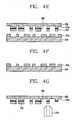
- inkis applied directly on the substrate and then partially removed using a cliché, such the remaining ink provides the desired pattern, as illustrated in FIGS. 4A to 4 G and FIGS. 5A to 5 G.
- a ink 250is applied to the entire surface of a substrate 240 , as illustrated in FIG. 4A and FIG. 5A .
- the substrate 240includes an etching object layer, and the ink 250 is applied onto the etching object layer.
- a cliché 230 having a plurality of convex patterns 230 ais formed, for example, from a transparent glass substrate.
- the clichémay be formed by depositing a metal layer on a glass substrate, and patterning the metal layer to form a metal pattern. Then, the glass substrate is etched using the metal pattern as a mask to form convex patterns as illustrated in FIG. 4B and FIG. 5B .
- the cliché 230having a plurality of convex patterns 230 a is prepared, and then an adhesion force intensifier 220 , for example, Hexa Methyl Disilazane (HMDS), is applied to the surface of the convex pattern 230 a using an adhesion force intensifying applicator 220 ′.
- HMDSHexa Methyl Disilazane
- an ink layer 250 applied onto the substrate 240is arranged to face the convex patterns 230 a of the cliché 230 .
- the substrate 240is positioned at a lower side and the cliché 230 is positioned at an upper side. Then, the cliché 230 is moved downward and applied with uniform pressure so that the convex patterns 230 a of the cliché 230 come into contact with the ink layer 250 .
- the substrate 240is moved downward to contact the ink layer 250 of the substrate 240 to the convex patterns 230 a of the cliché 230 .
- the ink 250 ′ in the regions that are in contact with the convex patterns 230 ais attached to the surfaces of the convex patterns 230 a and therefore removed from the substrate 240 . Accordingly, an ink pattern 250 a is formed on the substrate 240 , and the ink pattern 250 a remains at a region that is not in contact with the convex patterns 230 a of the cliché 230 .
- the adhesion force intensifier 220 applied to the surfaces of the convex patterns 230 aenhances the adhesion force between the cliché and the ink such that it is greater than the is adhesion force between the ink and the substrate 240 .
- the ink 250 ′ contacting the cliché 230is easily removed from the substrate 240 .
- ink in a region that is in contact with the convex patterns 230 a of the cliché 230is removed, and the ink pattern 250 a is formed at a region that is not in contact with the convex patterns 230 a .
- the convex patterns 230 a of the cliché 230have the same shape as the rest region except pattern regions to be formed on the substrate 240 .
- FIG. 4F and FIG. 5Fillustrates the ink pattern 250 a formed on the substrate 240 .
- An etching object layer of the substrateis etched by using the ink pattern 250 a as a mask to form a desired device pattern.
- the patternis harden by applying heat or irradiating with ultraviolet rays
- the etching object layermay be a metal layer for forming a gate electrode, a source/drain electrode, a gate line, a data line of a TFT, or a pixel electrode, a semiconductor layer for forming an active layer, or an insulating layer such as SiOx or SiNx.
- the ink pattern 250 aserves as a resist in the conventional photolithographic process.
- the ink pattern 250 ais formed on a metal layer or an insulating layer, and then the metal layer or the insulating layer is etched by a general etching process using the ink pattern 250 a as a mask, thereby forming a metal layer of a desired pattern (fore example, an electrode structure) or an insulating layer of a desired pattern (for example, a contact hole)
- a metal layer of a desired patternfore example, an electrode structure
- insulating layer of a desired patternfor example, a contact hole
- the ink 250 ′ and the adhesion force intensifier 220 applied to the surfaces of the convex patterns 230 a of the cliché 230can be removed from the cliché with a cleaning device 270 .
- Cleaning solution injected from the cleaning device 270removes the ink 250 ′ and the adhesion force intensifier 220 applied to the surfaces of the convex patterns 230 a .
- the cleaning solutioncan be acetone, N-Methyle Pyrolidone (NMP) and the like.
- the cleaning devicecan be a nozzle type which removes ink by spraying a cleaning solution from a nozzle.
- a roller type cleanermay be used. With the roller type cleaning device, a material capable of improving an adhesive force with respect to ink is applied onto the surface of a cleaning roller and the cleaning roller is rotated across the cliché thereby transferring the ink from the cliché to the surface of the cleaning roller. Accordingly, the ink applied onto the cliché can be removed.
- the ink in contact with convex patternsis separated from the substrate by contacting a cliché having convex patterns with a surface of the ink with uniform pressure applied thereto, so that ink patterns are formed at regions where they do not contact with the convex patterns.
- a cliché having convex patternscomes in contact with the ink to form printing patterns.
- printing equipmentcan be simplified because a printing roller is not used, processes are simplified compared to the case where the printing roller is used, and accuracy of patterns can be improved. By simplifying printing equipment and printing processes, production efficiency can be improved.
- the present inventionprovides a method for forming a pattern by a printing method, and more particularly, a method for forming a pattern, capable of forming ink patterns having a uniform thickness by using a cliché having convex patterns.
- the method for forming a pattern by a printing methodmay be used to form a device in a semiconductor substrate as well as an active device or a circuit of a display device such as a liquid crystal display device.
Landscapes
- Engineering & Computer Science (AREA)
- Physics & Mathematics (AREA)
- Chemical & Material Sciences (AREA)
- Nanotechnology (AREA)
- General Physics & Mathematics (AREA)
- Manufacturing & Machinery (AREA)
- Condensed Matter Physics & Semiconductors (AREA)
- Crystallography & Structural Chemistry (AREA)
- Microelectronics & Electronic Packaging (AREA)
- Computer Hardware Design (AREA)
- High Energy & Nuclear Physics (AREA)
- General Engineering & Computer Science (AREA)
- Power Engineering (AREA)
- Mathematical Physics (AREA)
- Theoretical Computer Science (AREA)
- Liquid Crystal (AREA)
- Printing Methods (AREA)
- Manufacturing Of Printed Circuit Boards (AREA)
- Exposure Of Semiconductors, Excluding Electron Or Ion Beam Exposure (AREA)
- Thin Film Transistor (AREA)
- Devices For Indicating Variable Information By Combining Individual Elements (AREA)
Abstract
Description
- This application claims the benefit of Korean Patent Application No. 30772, filed on Apr. 30, 2004, which is hereby incorporated by reference for all purposes as if fully set forth herein.
- 1. Field of the Invention
- The present invention relates to a printing method for forming a pattern in a liquid crystal display panel, and more particularly, to a method for forming a pattern with uniform thickness on a substrate.
- 2. Description of the Related Art
- A display device, especially, a flat panel display such as a liquid crystal display (LCD) device is driven by an active device such as a thin film transistor provided at each pixel. The driving method is referred as an active matrix driving method. According to the active matrix driving method, the active device is arranged at each pixel to drive the corresponding pixel.
FIG. 1 is a view illustrating an active matrix type LCD device. The LCD device is a TFT LCD device in which a thin film transistor is used as the active device. As illustrated, at each pixel of the TFT LCD device, wherein N×M pixels are arranged horizontally and vertically, a TFT formed at a gate line4 to which a scan signal is applied from an external driving circuit and adata line 6 to which an image signal is applied is provided. The TFT includes agate electrode 3 connected to the gate line4, asemiconductor layer 8 formed on thegate electrode 3 and activated as a scan signal is applied to thegate electrode 3, and a source/drain electrode 5 formed on thesemiconductor layer 8. Apixel electrode 10 is formed in a display region of the pixel1. Thepixel electrode 10 is connected to the source/drain electrode 5 and operates liquid crystal (not illustrated) by receiving an image signal through the source/drain electrode 5 as thesemiconductor layer 8 is activated.FIG. 2 is a view illustrating the structure of the TFT arranged at each pixel. As illustrated, the TFT includes a substrate20 formed of a transparent insulating material such as glass, agate electrode 3 formed on the substrate20, a gate insulating layer22 formed on the entire surface of the substrate20, asemiconductor layer 8 formed on the gate insulating layer22 and activated as a signal is applied to thegate electrode 3, a source/drain electrode 5 formed on the semiconductor layer, and a passivation layer25 formed on the source/drain electrode 5 for protecting the device.- The source/
drain electrode 5 of the TFT is electrically connected to a pixel electrode formed in the pixel region, and displays an image by driving liquid crystal as a signal is applied to the pixel electrode through the source/drain electrode 5. - In the active matrix type LCD device, each pixel has a size corresponding to several tens of μm. Accordingly, the active device such as the TFT arranged in the pixel has to be formed to have a minute size corresponding to several μm. Moreover, as the consumer's demand for a display device of a high image quality such as an HDTV is being increased, more pixels have to be arranged on a screen of the same area. Accordingly, an active device pattern arranged in each pixel (including a gate line pattern and a data line pattern) has to be also formed to have a minute size.
- In order to fabricate an active device such as a TFT according to the related art, a pattern, a line, and the like of the active device are formed using a photolithographic process using an exposing device. However, the photolithographic process includes a series of processes such as a photoresist deposition, an alignment process, an exposure process, a developing process, a cleaning process, and the like.
- Also, the photolithographic process must be repeated several times to form patterns of the liquid crystal display device, thereby lowering productivity.
- Accordingly, the present invention is directed to a printing method for forming a pattern that substantially obviates one or more of the problems due to limitations and disadvantages of the related art.
- Therefore, an advantage of the present invention is to provide a printing method for forming a pattern capable of improving productivity by forming patterns using a single process.
- Another advantage of the present invention is to provide a method for forming a pattern uniform thickness.
- Additional features and advantages of the invention will be set forth in the description which follows, and in part will be apparent from the description, or my be learned by practice of the invention. The objectives and other advantages of the invention will be realized and attained by the structure particularly pointed out in the written description and claims hereof as well as the appended drawings.
- To achieve these and other advantages and in accordance with the purpose of the present invention, as embodied and broadly described herein, there is provided A method for forming a pattern in a display device, comprising: providing a cliché having a plurality of convex patterns; applying an adhesive force reinforcing agent onto each surface of the plurality of convex patterns; forming an etching object layer on a substrate and then applying ink onto the etching object layer; attaching the cliché and the substrate to each other such that the convex patterns onto which the adhesive force reinforcing agent is applied contact the ink applied to the etching object layer; and forming ink patterns which selectively remain on the etching object layer by separating the substrate and the cliché from each other.
- It is to be understood that both the foregoing general description and the following detailed description are exemplary and explanatory and are intended to provide further explanation of the invention as claimed.
- The accompanying drawings, which are included to provide a further understanding of the invention and are incorporated in and constitute a part of this specification, illustrate embodiments of the invention and together with the description serve to explain the principles of the invention.
- In the drawings:
FIG. 1 is a plane view illustrating a structure of a typical liquid crystal display device;FIG. 2 is a cross-sectional diagram illustrating a structure of a thin film transistor of the liquid crystal display device illustrated inFIG. 1 ;FIGS. 3A to3C are views illustrating a gravure offset printing method for forming a pattern;FIGS. 4A to4G are views illustrating a method for forming a pattern in accordance with an embodiment of the present invention; andFIGS. 5A to5G are views illustrating a method for forming a pattern in accordance with the another embodiment of the present invention.- Reference will now be made in detail to embodiments of the present invention, examples of which are illustrated in the accompanying drawings.
- The present invention provides a printing method for forming a pattern for an active device of a display device like a liquid crystal display device. In particular, the present invention provides a gravure offset printing method in which ink is put on a concave plate, redundant ink is removed by scraping, and then printing is performed.
- In gravure offset printing, since ink is transferred to a substrate using a transfer roller, the pattern can be formed with a single transfer even in display devices having large display areas because the transfer roller used corresponds to the area of the desired display device. Gravure offset printing can be used to form various patterns for the display device such as a gate line and a data line connecting with a TFT, a pixel electrode, a metal pattern for a capacitor as well as the TFT, which constitute a liquid crystal display device.
FIGS. 3A to3C are views illustrating a printing method for forming ink patterns on a substrate. As illustrated inFIG. 3A , aftergrooves 132 are formed at specific positions on a concave plate or acliché 130, thegrooves 132 are filled ink134. Thegrooves 132 formed on thecliché 130 are formed by a photolithographic method. Theink 134 is filled in thegrooves 132 by applying theink 134 onto thecliché 130 and then pushing ablade 138 across the surface of thecliché 130. Thus, as theblade 138 is pushed, theink 134 is filled in thegrooves 132 and at the same time theink 130 remaining at the surface of thecliché 130 is removed.- As illustrated in
FIG. 3B , theink 134 filled in thegrooves 132 is transferred onto a surface of aprinting roller 131 as the roller is rotated across the surface of thecliché 130. Theprinting roller 131 is formed to have the same width as a the desired display panel to be fabricated, and has a circumference equal to a length of the panel. Accordingly, theink 134 is transferred onto the printing roller33 in a single pass across the cliché. - Thereafter, as illustrated in
FIG. 3C , theink 134 transferred to theprinting roller 131 is transferred onto anetching object layer 140 as theprinting roller 131 is rotated across the surface of theetching object layer 140 formed on asubstrate 130′. The transferredink 134 is dried by UV-irradiation or heat to formink patterns 133. The desiredpatterns 133 are formed on theetching object layer 140 of the display device in a single rotation of theprinting roller 131. Subsequently, theetching object layer 140 is etched using theink patterns 133 as a mask to form the desired patterns. - In the aforementioned printing method, the
cliché 130 and theprinting roller 131 are fabricated according to the size of a desired display device, such that the desired pattern can be transferred to thesubstrate 130′ in a single pass of theprinting roller 131. - The
etching object layer 140 may be a metal layer for forming a gate electrode, a source/drain electrode, a gate line, a data line of a TFT, or a pixel electrode, a semiconductor layer for forming an active layer, or an insulating layer such as SiOx or SiNx. - The
ink pattern 133 serves as a resist in the conventional photolithographic process. Accordingly, theink pattern 133 is formed on a metal layer or an insulating layer, and then the metal layer or the insulating layer is etched by a general etching process, thereby forming a metal layer of a desired pattern (for example, an electrode structure) or an insulating layer of a desired pattern (for example, a contact hole, etc.). - The above described printing method has many advantages. In particular, the printing method has a typical advantage that ink patterns are formed on a large area display unit with a single process or processes which are very simple in comparison to the photolithographic processes of the related art.
- As the size of the printing roller increases, the likelihood of a non-uniform pressure being applied to the substrate when the ink pattern is transferred from the surface of the printing roller increases. Accordingly, the ink pattern formed on the substrate may have a non-uniform thickness.
- To solve the problem, a method for forming a pattern on a substrate without using a printing roller is provided. Accordingly, to this embodiment of the invention ink is applied directly on the substrate and then partially removed using a cliché, such the remaining ink provides the desired pattern, as illustrated in
FIGS. 4A to4G andFIGS. 5A to5G. - According to this embodiment of the invention, a
ink 250 is applied to the entire surface of asubstrate 240, as illustrated inFIG. 4A andFIG. 5A . Thesubstrate 240 includes an etching object layer, and theink 250 is applied onto the etching object layer. - A
cliché 230 having a plurality ofconvex patterns 230ais formed, for example, from a transparent glass substrate. The cliché may be formed by depositing a metal layer on a glass substrate, and patterning the metal layer to form a metal pattern. Then, the glass substrate is etched using the metal pattern as a mask to form convex patterns as illustrated inFIG. 4B andFIG. 5B . Thecliché 230, having a plurality ofconvex patterns 230ais prepared, and then anadhesion force intensifier 220, for example, Hexa Methyl Disilazane (HMDS), is applied to the surface of theconvex pattern 230ausing an adhesionforce intensifying applicator 220′. - As illustrated in
FIG. 4C , anink layer 250 applied onto thesubstrate 240 is arranged to face theconvex patterns 230aof thecliché 230. Thesubstrate 240 is positioned at a lower side and thecliché 230 is positioned at an upper side. Then, thecliché 230 is moved downward and applied with uniform pressure so that theconvex patterns 230aof thecliché 230 come into contact with theink layer 250. - As illustrated in
FIG. 5C , it is also possible to position thesubstrate 240 at an upper side and to position thecliché 230 at a lower side. In this case, thesubstrate 240 is moved downward to contact theink layer 250 of thesubstrate 240 to theconvex patterns 230aof thecliché 230. - As illustrated in
FIG. 4E , when thecliché 230 is detached from thesubstrate 240, or thesubstrate 240 is detached from the cliché, as illustrated inFIG. 5E , theink 250′ in the regions that are in contact with theconvex patterns 230ais attached to the surfaces of theconvex patterns 230aand therefore removed from thesubstrate 240. Accordingly, anink pattern 250ais formed on thesubstrate 240, and theink pattern 250aremains at a region that is not in contact with theconvex patterns 230aof thecliché 230. Theadhesion force intensifier 220 applied to the surfaces of theconvex patterns 230aenhances the adhesion force between the cliché and the ink such that it is greater than the is adhesion force between the ink and thesubstrate 240. As a result, theink 250′ contacting thecliché 230 is easily removed from thesubstrate 240. Accordingly, ink in a region that is in contact with theconvex patterns 230aof thecliché 230 is removed, and theink pattern 250ais formed at a region that is not in contact with theconvex patterns 230a. Accordingly, theconvex patterns 230aof thecliché 230 have the same shape as the rest region except pattern regions to be formed on thesubstrate 240. FIG. 4F andFIG. 5F illustrates theink pattern 250aformed on thesubstrate 240. An etching object layer of the substrate is etched by using theink pattern 250aas a mask to form a desired device pattern. Before using theink pattern 250aas a mask, the pattern is harden by applying heat or irradiating with ultraviolet rays- The etching object layer may be a metal layer for forming a gate electrode, a source/drain electrode, a gate line, a data line of a TFT, or a pixel electrode, a semiconductor layer for forming an active layer, or an insulating layer such as SiOx or SiNx. When forming a pattern of a display device, the
ink pattern 250aserves as a resist in the conventional photolithographic process. Accordingly, theink pattern 250ais formed on a metal layer or an insulating layer, and then the metal layer or the insulating layer is etched by a general etching process using theink pattern 250aas a mask, thereby forming a metal layer of a desired pattern (fore example, an electrode structure) or an insulating layer of a desired pattern (for example, a contact hole) - M As illustrated in
FIG. 4G andFIG. 5G , theink 250′ and theadhesion force intensifier 220 applied to the surfaces of theconvex patterns 230aof thecliché 230 can be removed from the cliché with acleaning device 270. Cleaning solution injected from thecleaning device 270 removes theink 250′ and theadhesion force intensifier 220 applied to the surfaces of theconvex patterns 230a. For example, the cleaning solution can be acetone, N-Methyle Pyrolidone (NMP) and the like. - The cleaning device can be a nozzle type which removes ink by spraying a cleaning solution from a nozzle. In addition, though not illustrated in the drawings, a roller type cleaner may be used. With the roller type cleaning device, a material capable of improving an adhesive force with respect to ink is applied onto the surface of a cleaning roller and the cleaning roller is rotated across the cliché thereby transferring the ink from the cliché to the surface of the cleaning roller. Accordingly, the ink applied onto the cliché can be removed.
- According to the aforementioned embodiment of the present invention, after ink is applied onto a substrate on which a pattern is formed, the ink in contact with convex patterns is separated from the substrate by contacting a cliché having convex patterns with a surface of the ink with uniform pressure applied thereto, so that ink patterns are formed at regions where they do not contact with the convex patterns.
- After ink is pre-applied onto a substrate, a cliché having convex patterns comes in contact with the ink to form printing patterns. In such a case, printing equipment can be simplified because a printing roller is not used, processes are simplified compared to the case where the printing roller is used, and accuracy of patterns can be improved. By simplifying printing equipment and printing processes, production efficiency can be improved.
- As described so far, the present invention provides a method for forming a pattern by a printing method, and more particularly, a method for forming a pattern, capable of forming ink patterns having a uniform thickness by using a cliché having convex patterns.
- In addition, the method for forming a pattern by a printing method may be used to form a device in a semiconductor substrate as well as an active device or a circuit of a display device such as a liquid crystal display device.
- It will be apparent to those skilled in the art that various modifications and variation can be made in the present invention without departing from the spirit or scope of the invention. Thus, it is intended that the present invention cover the modifications and variations of this invention provided they come within the scope of the appended claims and their equivalents.
Claims (13)
Applications Claiming Priority (2)
| Application Number | Priority Date | Filing Date | Title |
|---|---|---|---|
| KR1020040030772AKR100631017B1 (en) | 2004-04-30 | 2004-04-30 | Pattern Forming Method Using Printing Method |
| KR2004-0030772 | 2004-04-30 |
Publications (2)
| Publication Number | Publication Date |
|---|---|
| US20050245085A1true US20050245085A1 (en) | 2005-11-03 |
| US7276445B2 US7276445B2 (en) | 2007-10-02 |
Family
ID=35187676
Family Applications (1)
| Application Number | Title | Priority Date | Filing Date |
|---|---|---|---|
| US11/114,095Expired - LifetimeUS7276445B2 (en) | 2004-04-30 | 2005-04-26 | Method for forming pattern using printing method |
Country Status (5)
| Country | Link |
|---|---|
| US (1) | US7276445B2 (en) |
| JP (1) | JP4322226B2 (en) |
| KR (1) | KR100631017B1 (en) |
| CN (1) | CN100363795C (en) |
| TW (1) | TWI252532B (en) |
Cited By (5)
| Publication number | Priority date | Publication date | Assignee | Title |
|---|---|---|---|---|
| US20070084367A1 (en)* | 2005-10-13 | 2007-04-19 | Yoo Hong S | Printing device system and patterning method using the same |
| US20070154655A1 (en)* | 2005-12-30 | 2007-07-05 | Lg.Philips Lcd Co., Ltd. | Liquid crystal display device having organic alignment layer and fabrication method thereof |
| US8470617B2 (en) | 2006-04-07 | 2013-06-25 | Qd Vision, Inc. | Composition including material, methods of depositing material, articles including same and systems for depositing material |
| US20150155339A1 (en)* | 2013-11-29 | 2015-06-04 | Tsinghua University | Method of making organic light emitting diode array |
| US9120149B2 (en) | 2006-06-24 | 2015-09-01 | Qd Vision, Inc. | Methods and articles including nanomaterial |
Families Citing this family (10)
| Publication number | Priority date | Publication date | Assignee | Title |
|---|---|---|---|---|
| KR101255294B1 (en)* | 2005-12-29 | 2013-04-23 | 엘지디스플레이 주식회사 | Printing Apparatus and Method of manufacturing Liquid Crystal Display Device using the same |
| KR101212151B1 (en) | 2005-12-29 | 2012-12-13 | 엘지디스플레이 주식회사 | Method of manufacturing Liquid Crystal Display Device using Patterning Method |
| US20080233280A1 (en)* | 2007-03-22 | 2008-09-25 | Graciela Beatriz Blanchet | Method to form a pattern of functional material on a substrate by treating a surface of a stamp |
| KR100957703B1 (en)* | 2007-04-13 | 2010-05-12 | 주식회사 엘지화학 | Fine pattern formation method |
| US8101519B2 (en) | 2008-08-14 | 2012-01-24 | Samsung Electronics Co., Ltd. | Mold, manufacturing method of mold, method for forming patterns using mold, and display substrate and display device manufactured by using method for forming patterns |
| KR101490484B1 (en) | 2008-09-26 | 2015-02-05 | 삼성디스플레이 주식회사 | Liquid crystal display device and manufacturing method thereof |
| CN102300802A (en)* | 2008-12-17 | 2011-12-28 | 3M创新有限公司 | Fabrication Of Conductive Nanostructures On A Flexible Substrate |
| CN102629077A (en)* | 2011-06-29 | 2012-08-08 | 北京京东方光电科技有限公司 | Preparation methods of resin dielectric layer and its material, liquid crystal panel and display member |
| KR101232828B1 (en) | 2012-02-23 | 2013-02-13 | 한국기계연구원 | Cliche with partition and method and apparatus for electronic printing |
| CN109076703A (en)* | 2016-04-15 | 2018-12-21 | 3M创新有限公司 | Electronic circuit is prepared by adhesive transfer |
Citations (2)
| Publication number | Priority date | Publication date | Assignee | Title |
|---|---|---|---|---|
| US6375870B1 (en)* | 1998-11-17 | 2002-04-23 | Corning Incorporated | Replicating a nanoscale pattern |
| US20050243233A1 (en)* | 2004-04-30 | 2005-11-03 | Chul-Ho Kim | Method for fabricating cliche and method for forming pattern using the same |
Family Cites Families (5)
| Publication number | Priority date | Publication date | Assignee | Title |
|---|---|---|---|---|
| KR100257811B1 (en)* | 1997-10-24 | 2000-06-01 | 구본준 | Fabrication method for lcd panel |
| KR100425856B1 (en)* | 1998-03-26 | 2004-06-18 | 엘지.필립스 엘시디 주식회사 | Method for etching layer to be etched |
| CN2349218Y (en)* | 1998-11-18 | 1999-11-17 | 中国科学院长春光学精密机械研究所 | Attached type mask assembly for quasi-molecule laser etching |
| JP2002280711A (en) | 2001-03-21 | 2002-09-27 | Fuji Photo Film Co Ltd | Method of forming metallic image and substrate |
| JP2003082469A (en) | 2001-09-13 | 2003-03-19 | Tdk Corp | Metallic film pattern forming method |
- 2004
- 2004-04-30KRKR1020040030772Apatent/KR100631017B1/ennot_activeExpired - Fee Related
- 2005
- 2005-04-26USUS11/114,095patent/US7276445B2/ennot_activeExpired - Lifetime
- 2005-04-27TWTW094113544Apatent/TWI252532B/ennot_activeIP Right Cessation
- 2005-04-28JPJP2005131066Apatent/JP4322226B2/ennot_activeExpired - Fee Related
- 2005-04-28CNCNB2005100700029Apatent/CN100363795C/ennot_activeExpired - Fee Related
Patent Citations (2)
| Publication number | Priority date | Publication date | Assignee | Title |
|---|---|---|---|---|
| US6375870B1 (en)* | 1998-11-17 | 2002-04-23 | Corning Incorporated | Replicating a nanoscale pattern |
| US20050243233A1 (en)* | 2004-04-30 | 2005-11-03 | Chul-Ho Kim | Method for fabricating cliche and method for forming pattern using the same |
Cited By (15)
| Publication number | Priority date | Publication date | Assignee | Title |
|---|---|---|---|---|
| US20070084367A1 (en)* | 2005-10-13 | 2007-04-19 | Yoo Hong S | Printing device system and patterning method using the same |
| US8629961B2 (en) | 2005-12-30 | 2014-01-14 | Lg Display Co., Ltd. | Liquid crystal display device having organic alignment layer and fabrication method thereof |
| US20070154655A1 (en)* | 2005-12-30 | 2007-07-05 | Lg.Philips Lcd Co., Ltd. | Liquid crystal display device having organic alignment layer and fabrication method thereof |
| US7755731B2 (en)* | 2005-12-30 | 2010-07-13 | Lg Display Co., Ltd. | Liquid crystal display device having organic alignment layer and fabrication method thereof |
| US20100260937A1 (en)* | 2005-12-30 | 2010-10-14 | Lg Display Co., Ltd. | Liquid crystal display device having organic alignment layer and fabrication method thereof |
| US8039063B2 (en) | 2005-12-30 | 2011-10-18 | Lg Display Co., Ltd. | Liquid crystal display device having organic alignment layer and fabrication method thereof |
| US8345200B2 (en) | 2005-12-30 | 2013-01-01 | Lg Display Co., Ltd. | Liquid crystal display device having organic alignment layer and fabrication method thereof |
| US8470617B2 (en) | 2006-04-07 | 2013-06-25 | Qd Vision, Inc. | Composition including material, methods of depositing material, articles including same and systems for depositing material |
| US8906804B2 (en) | 2006-04-07 | 2014-12-09 | Qd Vision, Inc. | Composition including material, methods of depositing material, articles including same and systems for depositing materials |
| US9034669B2 (en) | 2006-04-07 | 2015-05-19 | Qd Vision, Inc. | Methods of depositing nanomaterial and methods of making a device |
| US9252013B2 (en) | 2006-04-07 | 2016-02-02 | Qd Vision, Inc. | Methods and articles including nanomaterial |
| US9390920B2 (en) | 2006-04-07 | 2016-07-12 | Qd Vision, Inc. | Composition including material, methods of depositing material, articles including same and systems for depositing material |
| US9120149B2 (en) | 2006-06-24 | 2015-09-01 | Qd Vision, Inc. | Methods and articles including nanomaterial |
| US20150155339A1 (en)* | 2013-11-29 | 2015-06-04 | Tsinghua University | Method of making organic light emitting diode array |
| US9305978B2 (en)* | 2013-11-29 | 2016-04-05 | Tsinghua University | Method of making organic light emitting diode array |
Also Published As
| Publication number | Publication date |
|---|---|
| CN100363795C (en) | 2008-01-23 |
| TW200536006A (en) | 2005-11-01 |
| KR100631017B1 (en) | 2006-10-04 |
| CN1693955A (en) | 2005-11-09 |
| JP2005354042A (en) | 2005-12-22 |
| TWI252532B (en) | 2006-04-01 |
| KR20050105048A (en) | 2005-11-03 |
| US7276445B2 (en) | 2007-10-02 |
| JP4322226B2 (en) | 2009-08-26 |
Similar Documents
| Publication | Publication Date | Title |
|---|---|---|
| US7361285B2 (en) | Method for fabricating cliche and method for forming pattern using the same | |
| CN100575077C (en) | Printing apparatus for liquid crystal display device | |
| US7276445B2 (en) | Method for forming pattern using printing method | |
| US6940578B2 (en) | Method for fabricating liquid crystal display device | |
| KR101339170B1 (en) | Liquid crystal display panel and manufacturing method thereof | |
| US7704678B2 (en) | Method of manufacturing printing plate and method of manufacturing liquid crystal display device using the same | |
| KR101308441B1 (en) | Appartus For Fabricating Thin Film Pattern And Method For Fabricating Using The Same | |
| CN101266950A (en) | Method for manufacturing array substrate for liquid crystal display device | |
| US7441500B2 (en) | Method for forming printing roll patterns | |
| US6875704B2 (en) | Method for forming pattern using printing process | |
| US7520220B2 (en) | Cliché unit, printing apparatus, and printing method using the same | |
| KR100631016B1 (en) | Manufacturing method of printing roll used for pattern formation by printing method and pattern forming method using the same | |
| KR20080062952A (en) | Printing roll, manufacturing method of liquid crystal display device using the same | |
| US20070165181A1 (en) | Apparatus for fabricating flat panel display device and method for fabricating thereof | |
| KR100631015B1 (en) | Manufacturing method of printing roll and pattern forming method using the same | |
| US20040149683A1 (en) | Method for forming pattern using printing process | |
| JPH0667135A (en) | Liquid crystal display manufacturing method | |
| US6930733B2 (en) | Liquid crystal display device and fabrication method thereof | |
| KR100922797B1 (en) | Pattern Forming Device and Forming Method | |
| US20060160033A1 (en) | Method for printing by printed pattern and production equipment for printing printed pattern | |
| US7441502B2 (en) | Printing apparatus and method for forming patterns for liquid crystal display device using the same | |
| KR20070114901A (en) | Thin film transistor substrate and its manufacturing method | |
| KR20050053199A (en) | Method for fabricating liquid crystal display device | |
| KR20090070134A (en) | Manufacturing Method of Flat Panel Display | |
| KR20080062953A (en) | Pattern Forming Method by Printing Method |
Legal Events
| Date | Code | Title | Description |
|---|---|---|---|
| AS | Assignment | Owner name:LG.PHILIPS LCD CO., LTD., KOREA, REPUBLIC OF Free format text:ASSIGNMENT OF ASSIGNORS INTEREST;ASSIGNOR:YOO, HONG-SUK;REEL/FRAME:016508/0267 Effective date:20050419 | |
| STCF | Information on status: patent grant | Free format text:PATENTED CASE | |
| FEPP | Fee payment procedure | Free format text:PAYOR NUMBER ASSIGNED (ORIGINAL EVENT CODE: ASPN); ENTITY STATUS OF PATENT OWNER: LARGE ENTITY | |
| AS | Assignment | Owner name:LG DISPLAY CO., LTD., KOREA, REPUBLIC OF Free format text:CHANGE OF NAME;ASSIGNOR:LG.PHILIPS LCD CO., LTD.;REEL/FRAME:021763/0212 Effective date:20080304 | |
| FEPP | Fee payment procedure | Free format text:PAYER NUMBER DE-ASSIGNED (ORIGINAL EVENT CODE: RMPN); ENTITY STATUS OF PATENT OWNER: LARGE ENTITY Free format text:PAYOR NUMBER ASSIGNED (ORIGINAL EVENT CODE: ASPN); ENTITY STATUS OF PATENT OWNER: LARGE ENTITY | |
| FPAY | Fee payment | Year of fee payment:4 | |
| FPAY | Fee payment | Year of fee payment:8 | |
| MAFP | Maintenance fee payment | Free format text:PAYMENT OF MAINTENANCE FEE, 12TH YEAR, LARGE ENTITY (ORIGINAL EVENT CODE: M1553); ENTITY STATUS OF PATENT OWNER: LARGE ENTITY Year of fee payment:12 |