US20050242446A1 - Integrated circuit package with different hardness bump pad and bump and manufacturing method therefor - Google Patents
Integrated circuit package with different hardness bump pad and bump and manufacturing method thereforDownload PDFInfo
- Publication number
- US20050242446A1 US20050242446A1US10/908,254US90825405AUS2005242446A1US 20050242446 A1US20050242446 A1US 20050242446A1US 90825405 AUS90825405 AUS 90825405AUS 2005242446 A1US2005242446 A1US 2005242446A1
- Authority
- US
- United States
- Prior art keywords
- bump
- pad
- forming
- integrated circuit
- contact pad
- Prior art date
- Legal status (The legal status is an assumption and is not a legal conclusion. Google has not performed a legal analysis and makes no representation as to the accuracy of the status listed.)
- Abandoned
Links
- 238000004519manufacturing processMethods0.000titleclaimsabstractdescription10
- 238000002161passivationMethods0.000claimsabstractdescription36
- 238000005272metallurgyMethods0.000claimsabstractdescription22
- 238000000034methodMethods0.000claimsabstractdescription19
- 239000000463materialSubstances0.000claimsabstractdescription18
- PXHVJJICTQNCMI-UHFFFAOYSA-NNickelChemical compound[Ni]PXHVJJICTQNCMI-UHFFFAOYSA-N0.000claimsdescription18
- PCHJSUWPFVWCPO-UHFFFAOYSA-NgoldChemical compound[Au]PCHJSUWPFVWCPO-UHFFFAOYSA-N0.000claimsdescription18
- 239000010931goldSubstances0.000claimsdescription18
- 229910052737goldInorganic materials0.000claimsdescription18
- 229920002120photoresistant polymerPolymers0.000claimsdescription11
- 229910052759nickelInorganic materials0.000claimsdescription9
- 229910000838Al alloyInorganic materials0.000claimsdescription8
- XAGFODPZIPBFFR-UHFFFAOYSA-NaluminiumChemical compound[Al]XAGFODPZIPBFFR-UHFFFAOYSA-N0.000claimsdescription8
- 229910000990Ni alloyInorganic materials0.000claimsdescription7
- 229910052782aluminiumInorganic materials0.000claimsdescription7
- 238000005260corrosionMethods0.000claimsdescription6
- 229910001020Au alloyInorganic materials0.000claimsdescription5
- 230000007797corrosionEffects0.000claimsdescription5
- 239000003353gold alloySubstances0.000claimsdescription5
- 238000007747platingMethods0.000description13
- 238000005530etchingMethods0.000description5
- RYGMFSIKBFXOCR-UHFFFAOYSA-NCopperChemical compound[Cu]RYGMFSIKBFXOCR-UHFFFAOYSA-N0.000description4
- 238000005516engineering processMethods0.000description4
- 229910052802copperInorganic materials0.000description3
- 239000010949copperSubstances0.000description3
- 238000000151depositionMethods0.000description3
- 230000008021depositionEffects0.000description3
- 229910052751metalInorganic materials0.000description3
- 239000002184metalSubstances0.000description3
- 238000000637aluminium metallisationMethods0.000description2
- 238000011161developmentMethods0.000description2
- 230000018109developmental processEffects0.000description2
- 229910001092metal group alloyInorganic materials0.000description2
- 238000012986modificationMethods0.000description2
- 230000004048modificationEffects0.000description2
- 238000001020plasma etchingMethods0.000description2
- 238000004544sputter depositionMethods0.000description2
- 239000000758substrateSubstances0.000description2
- VYZAMTAEIAYCRO-UHFFFAOYSA-NChromiumChemical compound[Cr]VYZAMTAEIAYCRO-UHFFFAOYSA-N0.000description1
- 239000004642PolyimideSubstances0.000description1
- 229910052581Si3N4Inorganic materials0.000description1
- VYPSYNLAJGMNEJ-UHFFFAOYSA-NSilicium dioxideChemical compoundO=[Si]=OVYPSYNLAJGMNEJ-UHFFFAOYSA-N0.000description1
- XUIMIQQOPSSXEZ-UHFFFAOYSA-NSiliconChemical compound[Si]XUIMIQQOPSSXEZ-UHFFFAOYSA-N0.000description1
- ATJFFYVFTNAWJD-UHFFFAOYSA-NTinChemical compound[Sn]ATJFFYVFTNAWJD-UHFFFAOYSA-N0.000description1
- 229910001080W alloyInorganic materials0.000description1
- 239000002253acidSubstances0.000description1
- 238000004140cleaningMethods0.000description1
- 239000003989dielectric materialSubstances0.000description1
- 238000009713electroplatingMethods0.000description1
- 230000008020evaporationEffects0.000description1
- 238000001704evaporationMethods0.000description1
- 230000003203everyday effectEffects0.000description1
- 238000000059patterningMethods0.000description1
- 239000004033plasticSubstances0.000description1
- 229920001721polyimidePolymers0.000description1
- 238000004886process controlMethods0.000description1
- 230000001681protective effectEffects0.000description1
- 230000009467reductionEffects0.000description1
- 239000004065semiconductorSubstances0.000description1
- 229910052710siliconInorganic materials0.000description1
- 239000010703siliconSubstances0.000description1
- HQVNEWCFYHHQES-UHFFFAOYSA-Nsilicon nitrideChemical compoundN12[Si]34N5[Si]62N3[Si]51N64HQVNEWCFYHHQES-UHFFFAOYSA-N0.000description1
- 229910052814silicon oxideInorganic materials0.000description1
- 238000005549size reductionMethods0.000description1
- 239000010409thin filmSubstances0.000description1
- 238000000427thin-film depositionMethods0.000description1
- 229910052718tinInorganic materials0.000description1
- 239000011135tinSubstances0.000description1
- MAKDTFFYCIMFQP-UHFFFAOYSA-Ntitanium tungstenChemical compound[Ti].[W]MAKDTFFYCIMFQP-UHFFFAOYSA-N0.000description1
Images

Classifications
- H—ELECTRICITY
- H01—ELECTRIC ELEMENTS
- H01L—SEMICONDUCTOR DEVICES NOT COVERED BY CLASS H10
- H01L24/00—Arrangements for connecting or disconnecting semiconductor or solid-state bodies; Methods or apparatus related thereto
- H01L24/01—Means for bonding being attached to, or being formed on, the surface to be connected, e.g. chip-to-package, die-attach, "first-level" interconnects; Manufacturing methods related thereto
- H01L24/02—Bonding areas ; Manufacturing methods related thereto
- H01L24/04—Structure, shape, material or disposition of the bonding areas prior to the connecting process
- H01L24/05—Structure, shape, material or disposition of the bonding areas prior to the connecting process of an individual bonding area
- H—ELECTRICITY
- H01—ELECTRIC ELEMENTS
- H01L—SEMICONDUCTOR DEVICES NOT COVERED BY CLASS H10
- H01L24/00—Arrangements for connecting or disconnecting semiconductor or solid-state bodies; Methods or apparatus related thereto
- H01L24/01—Means for bonding being attached to, or being formed on, the surface to be connected, e.g. chip-to-package, die-attach, "first-level" interconnects; Manufacturing methods related thereto
- H01L24/10—Bump connectors ; Manufacturing methods related thereto
- H01L24/12—Structure, shape, material or disposition of the bump connectors prior to the connecting process
- H01L24/13—Structure, shape, material or disposition of the bump connectors prior to the connecting process of an individual bump connector
- H—ELECTRICITY
- H01—ELECTRIC ELEMENTS
- H01L—SEMICONDUCTOR DEVICES NOT COVERED BY CLASS H10
- H01L2224/00—Indexing scheme for arrangements for connecting or disconnecting semiconductor or solid-state bodies and methods related thereto as covered by H01L24/00
- H01L2224/01—Means for bonding being attached to, or being formed on, the surface to be connected, e.g. chip-to-package, die-attach, "first-level" interconnects; Manufacturing methods related thereto
- H01L2224/02—Bonding areas; Manufacturing methods related thereto
- H01L2224/03—Manufacturing methods
- H01L2224/034—Manufacturing methods by blanket deposition of the material of the bonding area
- H01L2224/0346—Plating
- H—ELECTRICITY
- H01—ELECTRIC ELEMENTS
- H01L—SEMICONDUCTOR DEVICES NOT COVERED BY CLASS H10
- H01L2224/00—Indexing scheme for arrangements for connecting or disconnecting semiconductor or solid-state bodies and methods related thereto as covered by H01L24/00
- H01L2224/01—Means for bonding being attached to, or being formed on, the surface to be connected, e.g. chip-to-package, die-attach, "first-level" interconnects; Manufacturing methods related thereto
- H01L2224/02—Bonding areas; Manufacturing methods related thereto
- H01L2224/03—Manufacturing methods
- H01L2224/0347—Manufacturing methods using a lift-off mask
- H—ELECTRICITY
- H01—ELECTRIC ELEMENTS
- H01L—SEMICONDUCTOR DEVICES NOT COVERED BY CLASS H10
- H01L2224/00—Indexing scheme for arrangements for connecting or disconnecting semiconductor or solid-state bodies and methods related thereto as covered by H01L24/00
- H01L2224/01—Means for bonding being attached to, or being formed on, the surface to be connected, e.g. chip-to-package, die-attach, "first-level" interconnects; Manufacturing methods related thereto
- H01L2224/02—Bonding areas; Manufacturing methods related thereto
- H01L2224/03—Manufacturing methods
- H01L2224/039—Methods of manufacturing bonding areas involving a specific sequence of method steps
- H01L2224/03914—Methods of manufacturing bonding areas involving a specific sequence of method steps the bonding area, e.g. under bump metallisation [UBM], being used as a mask for patterning other parts
- H—ELECTRICITY
- H01—ELECTRIC ELEMENTS
- H01L—SEMICONDUCTOR DEVICES NOT COVERED BY CLASS H10
- H01L2224/00—Indexing scheme for arrangements for connecting or disconnecting semiconductor or solid-state bodies and methods related thereto as covered by H01L24/00
- H01L2224/01—Means for bonding being attached to, or being formed on, the surface to be connected, e.g. chip-to-package, die-attach, "first-level" interconnects; Manufacturing methods related thereto
- H01L2224/02—Bonding areas; Manufacturing methods related thereto
- H01L2224/04—Structure, shape, material or disposition of the bonding areas prior to the connecting process
- H01L2224/05—Structure, shape, material or disposition of the bonding areas prior to the connecting process of an individual bonding area
- H01L2224/05001—Internal layers
- H01L2224/0502—Disposition
- H01L2224/05022—Disposition the internal layer being at least partially embedded in the surface
- H—ELECTRICITY
- H01—ELECTRIC ELEMENTS
- H01L—SEMICONDUCTOR DEVICES NOT COVERED BY CLASS H10
- H01L2224/00—Indexing scheme for arrangements for connecting or disconnecting semiconductor or solid-state bodies and methods related thereto as covered by H01L24/00
- H01L2224/01—Means for bonding being attached to, or being formed on, the surface to be connected, e.g. chip-to-package, die-attach, "first-level" interconnects; Manufacturing methods related thereto
- H01L2224/02—Bonding areas; Manufacturing methods related thereto
- H01L2224/04—Structure, shape, material or disposition of the bonding areas prior to the connecting process
- H01L2224/05—Structure, shape, material or disposition of the bonding areas prior to the connecting process of an individual bonding area
- H01L2224/05001—Internal layers
- H01L2224/0502—Disposition
- H01L2224/05026—Disposition the internal layer being disposed in a recess of the surface
- H01L2224/05027—Disposition the internal layer being disposed in a recess of the surface the internal layer extending out of an opening
- H—ELECTRICITY
- H01—ELECTRIC ELEMENTS
- H01L—SEMICONDUCTOR DEVICES NOT COVERED BY CLASS H10
- H01L2224/00—Indexing scheme for arrangements for connecting or disconnecting semiconductor or solid-state bodies and methods related thereto as covered by H01L24/00
- H01L2224/01—Means for bonding being attached to, or being formed on, the surface to be connected, e.g. chip-to-package, die-attach, "first-level" interconnects; Manufacturing methods related thereto
- H01L2224/02—Bonding areas; Manufacturing methods related thereto
- H01L2224/04—Structure, shape, material or disposition of the bonding areas prior to the connecting process
- H01L2224/05—Structure, shape, material or disposition of the bonding areas prior to the connecting process of an individual bonding area
- H01L2224/05001—Internal layers
- H01L2224/05099—Material
- H01L2224/051—Material with a principal constituent of the material being a metal or a metalloid, e.g. boron [B], silicon [Si], germanium [Ge], arsenic [As], antimony [Sb], tellurium [Te] and polonium [Po], and alloys thereof
- H01L2224/05117—Material with a principal constituent of the material being a metal or a metalloid, e.g. boron [B], silicon [Si], germanium [Ge], arsenic [As], antimony [Sb], tellurium [Te] and polonium [Po], and alloys thereof the principal constituent melting at a temperature of greater than or equal to 400°C and less than 950°C
- H01L2224/05124—Aluminium [Al] as principal constituent
- H—ELECTRICITY
- H01—ELECTRIC ELEMENTS
- H01L—SEMICONDUCTOR DEVICES NOT COVERED BY CLASS H10
- H01L2224/00—Indexing scheme for arrangements for connecting or disconnecting semiconductor or solid-state bodies and methods related thereto as covered by H01L24/00
- H01L2224/01—Means for bonding being attached to, or being formed on, the surface to be connected, e.g. chip-to-package, die-attach, "first-level" interconnects; Manufacturing methods related thereto
- H01L2224/02—Bonding areas; Manufacturing methods related thereto
- H01L2224/04—Structure, shape, material or disposition of the bonding areas prior to the connecting process
- H01L2224/05—Structure, shape, material or disposition of the bonding areas prior to the connecting process of an individual bonding area
- H01L2224/05001—Internal layers
- H01L2224/05099—Material
- H01L2224/051—Material with a principal constituent of the material being a metal or a metalloid, e.g. boron [B], silicon [Si], germanium [Ge], arsenic [As], antimony [Sb], tellurium [Te] and polonium [Po], and alloys thereof
- H01L2224/05163—Material with a principal constituent of the material being a metal or a metalloid, e.g. boron [B], silicon [Si], germanium [Ge], arsenic [As], antimony [Sb], tellurium [Te] and polonium [Po], and alloys thereof the principal constituent melting at a temperature of greater than 1550°C
- H01L2224/05166—Titanium [Ti] as principal constituent
- H—ELECTRICITY
- H01—ELECTRIC ELEMENTS
- H01L—SEMICONDUCTOR DEVICES NOT COVERED BY CLASS H10
- H01L2224/00—Indexing scheme for arrangements for connecting or disconnecting semiconductor or solid-state bodies and methods related thereto as covered by H01L24/00
- H01L2224/01—Means for bonding being attached to, or being formed on, the surface to be connected, e.g. chip-to-package, die-attach, "first-level" interconnects; Manufacturing methods related thereto
- H01L2224/02—Bonding areas; Manufacturing methods related thereto
- H01L2224/04—Structure, shape, material or disposition of the bonding areas prior to the connecting process
- H01L2224/05—Structure, shape, material or disposition of the bonding areas prior to the connecting process of an individual bonding area
- H01L2224/0554—External layer
- H01L2224/0556—Disposition
- H01L2224/05571—Disposition the external layer being disposed in a recess of the surface
- H01L2224/05572—Disposition the external layer being disposed in a recess of the surface the external layer extending out of an opening
- H—ELECTRICITY
- H01—ELECTRIC ELEMENTS
- H01L—SEMICONDUCTOR DEVICES NOT COVERED BY CLASS H10
- H01L2224/00—Indexing scheme for arrangements for connecting or disconnecting semiconductor or solid-state bodies and methods related thereto as covered by H01L24/00
- H01L2224/01—Means for bonding being attached to, or being formed on, the surface to be connected, e.g. chip-to-package, die-attach, "first-level" interconnects; Manufacturing methods related thereto
- H01L2224/02—Bonding areas; Manufacturing methods related thereto
- H01L2224/04—Structure, shape, material or disposition of the bonding areas prior to the connecting process
- H01L2224/05—Structure, shape, material or disposition of the bonding areas prior to the connecting process of an individual bonding area
- H01L2224/0554—External layer
- H01L2224/05575—Plural external layers
- H01L2224/0558—Plural external layers being stacked
- H01L2224/05582—Two-layer coating
- H—ELECTRICITY
- H01—ELECTRIC ELEMENTS
- H01L—SEMICONDUCTOR DEVICES NOT COVERED BY CLASS H10
- H01L2224/00—Indexing scheme for arrangements for connecting or disconnecting semiconductor or solid-state bodies and methods related thereto as covered by H01L24/00
- H01L2224/01—Means for bonding being attached to, or being formed on, the surface to be connected, e.g. chip-to-package, die-attach, "first-level" interconnects; Manufacturing methods related thereto
- H01L2224/02—Bonding areas; Manufacturing methods related thereto
- H01L2224/04—Structure, shape, material or disposition of the bonding areas prior to the connecting process
- H01L2224/05—Structure, shape, material or disposition of the bonding areas prior to the connecting process of an individual bonding area
- H01L2224/0554—External layer
- H01L2224/05599—Material
- H01L2224/056—Material with a principal constituent of the material being a metal or a metalloid, e.g. boron [B], silicon [Si], germanium [Ge], arsenic [As], antimony [Sb], tellurium [Te] and polonium [Po], and alloys thereof
- H01L2224/05638—Material with a principal constituent of the material being a metal or a metalloid, e.g. boron [B], silicon [Si], germanium [Ge], arsenic [As], antimony [Sb], tellurium [Te] and polonium [Po], and alloys thereof the principal constituent melting at a temperature of greater than or equal to 950°C and less than 1550°C
- H01L2224/05644—Gold [Au] as principal constituent
- H—ELECTRICITY
- H01—ELECTRIC ELEMENTS
- H01L—SEMICONDUCTOR DEVICES NOT COVERED BY CLASS H10
- H01L2224/00—Indexing scheme for arrangements for connecting or disconnecting semiconductor or solid-state bodies and methods related thereto as covered by H01L24/00
- H01L2224/01—Means for bonding being attached to, or being formed on, the surface to be connected, e.g. chip-to-package, die-attach, "first-level" interconnects; Manufacturing methods related thereto
- H01L2224/10—Bump connectors; Manufacturing methods related thereto
- H01L2224/11—Manufacturing methods
- H01L2224/114—Manufacturing methods by blanket deposition of the material of the bump connector
- H01L2224/1146—Plating
- H—ELECTRICITY
- H01—ELECTRIC ELEMENTS
- H01L—SEMICONDUCTOR DEVICES NOT COVERED BY CLASS H10
- H01L2224/00—Indexing scheme for arrangements for connecting or disconnecting semiconductor or solid-state bodies and methods related thereto as covered by H01L24/00
- H01L2224/01—Means for bonding being attached to, or being formed on, the surface to be connected, e.g. chip-to-package, die-attach, "first-level" interconnects; Manufacturing methods related thereto
- H01L2224/10—Bump connectors; Manufacturing methods related thereto
- H01L2224/11—Manufacturing methods
- H01L2224/1147—Manufacturing methods using a lift-off mask
- H—ELECTRICITY
- H01—ELECTRIC ELEMENTS
- H01L—SEMICONDUCTOR DEVICES NOT COVERED BY CLASS H10
- H01L2224/00—Indexing scheme for arrangements for connecting or disconnecting semiconductor or solid-state bodies and methods related thereto as covered by H01L24/00
- H01L2224/01—Means for bonding being attached to, or being formed on, the surface to be connected, e.g. chip-to-package, die-attach, "first-level" interconnects; Manufacturing methods related thereto
- H01L2224/10—Bump connectors; Manufacturing methods related thereto
- H01L2224/11—Manufacturing methods
- H01L2224/119—Methods of manufacturing bump connectors involving a specific sequence of method steps
- H01L2224/11901—Methods of manufacturing bump connectors involving a specific sequence of method steps with repetition of the same manufacturing step
- H01L2224/11902—Multiple masking steps
- H01L2224/11906—Multiple masking steps with modification of the same mask
- H—ELECTRICITY
- H01—ELECTRIC ELEMENTS
- H01L—SEMICONDUCTOR DEVICES NOT COVERED BY CLASS H10
- H01L2224/00—Indexing scheme for arrangements for connecting or disconnecting semiconductor or solid-state bodies and methods related thereto as covered by H01L24/00
- H01L2224/01—Means for bonding being attached to, or being formed on, the surface to be connected, e.g. chip-to-package, die-attach, "first-level" interconnects; Manufacturing methods related thereto
- H01L2224/10—Bump connectors; Manufacturing methods related thereto
- H01L2224/12—Structure, shape, material or disposition of the bump connectors prior to the connecting process
- H01L2224/13—Structure, shape, material or disposition of the bump connectors prior to the connecting process of an individual bump connector
- H01L2224/13001—Core members of the bump connector
- H01L2224/13099—Material
- H01L2224/131—Material with a principal constituent of the material being a metal or a metalloid, e.g. boron [B], silicon [Si], germanium [Ge], arsenic [As], antimony [Sb], tellurium [Te] and polonium [Po], and alloys thereof
- H01L2224/13138—Material with a principal constituent of the material being a metal or a metalloid, e.g. boron [B], silicon [Si], germanium [Ge], arsenic [As], antimony [Sb], tellurium [Te] and polonium [Po], and alloys thereof the principal constituent melting at a temperature of greater than or equal to 950°C and less than 1550°C
- H01L2224/13144—Gold [Au] as principal constituent
- H—ELECTRICITY
- H01—ELECTRIC ELEMENTS
- H01L—SEMICONDUCTOR DEVICES NOT COVERED BY CLASS H10
- H01L24/00—Arrangements for connecting or disconnecting semiconductor or solid-state bodies; Methods or apparatus related thereto
- H01L24/01—Means for bonding being attached to, or being formed on, the surface to be connected, e.g. chip-to-package, die-attach, "first-level" interconnects; Manufacturing methods related thereto
- H01L24/02—Bonding areas ; Manufacturing methods related thereto
- H01L24/03—Manufacturing methods
- H—ELECTRICITY
- H01—ELECTRIC ELEMENTS
- H01L—SEMICONDUCTOR DEVICES NOT COVERED BY CLASS H10
- H01L24/00—Arrangements for connecting or disconnecting semiconductor or solid-state bodies; Methods or apparatus related thereto
- H01L24/01—Means for bonding being attached to, or being formed on, the surface to be connected, e.g. chip-to-package, die-attach, "first-level" interconnects; Manufacturing methods related thereto
- H01L24/10—Bump connectors ; Manufacturing methods related thereto
- H01L24/11—Manufacturing methods
- H—ELECTRICITY
- H01—ELECTRIC ELEMENTS
- H01L—SEMICONDUCTOR DEVICES NOT COVERED BY CLASS H10
- H01L2924/00—Indexing scheme for arrangements or methods for connecting or disconnecting semiconductor or solid-state bodies as covered by H01L24/00
- H01L2924/0001—Technical content checked by a classifier
- H—ELECTRICITY
- H01—ELECTRIC ELEMENTS
- H01L—SEMICONDUCTOR DEVICES NOT COVERED BY CLASS H10
- H01L2924/00—Indexing scheme for arrangements or methods for connecting or disconnecting semiconductor or solid-state bodies as covered by H01L24/00
- H01L2924/01—Chemical elements
- H01L2924/01013—Aluminum [Al]
- H—ELECTRICITY
- H01—ELECTRIC ELEMENTS
- H01L—SEMICONDUCTOR DEVICES NOT COVERED BY CLASS H10
- H01L2924/00—Indexing scheme for arrangements or methods for connecting or disconnecting semiconductor or solid-state bodies as covered by H01L24/00
- H01L2924/01—Chemical elements
- H01L2924/01022—Titanium [Ti]
- H—ELECTRICITY
- H01—ELECTRIC ELEMENTS
- H01L—SEMICONDUCTOR DEVICES NOT COVERED BY CLASS H10
- H01L2924/00—Indexing scheme for arrangements or methods for connecting or disconnecting semiconductor or solid-state bodies as covered by H01L24/00
- H01L2924/01—Chemical elements
- H01L2924/01027—Cobalt [Co]
- H—ELECTRICITY
- H01—ELECTRIC ELEMENTS
- H01L—SEMICONDUCTOR DEVICES NOT COVERED BY CLASS H10
- H01L2924/00—Indexing scheme for arrangements or methods for connecting or disconnecting semiconductor or solid-state bodies as covered by H01L24/00
- H01L2924/01—Chemical elements
- H01L2924/01029—Copper [Cu]
- H—ELECTRICITY
- H01—ELECTRIC ELEMENTS
- H01L—SEMICONDUCTOR DEVICES NOT COVERED BY CLASS H10
- H01L2924/00—Indexing scheme for arrangements or methods for connecting or disconnecting semiconductor or solid-state bodies as covered by H01L24/00
- H01L2924/01—Chemical elements
- H01L2924/01033—Arsenic [As]
- H—ELECTRICITY
- H01—ELECTRIC ELEMENTS
- H01L—SEMICONDUCTOR DEVICES NOT COVERED BY CLASS H10
- H01L2924/00—Indexing scheme for arrangements or methods for connecting or disconnecting semiconductor or solid-state bodies as covered by H01L24/00
- H01L2924/01—Chemical elements
- H01L2924/01074—Tungsten [W]
- H—ELECTRICITY
- H01—ELECTRIC ELEMENTS
- H01L—SEMICONDUCTOR DEVICES NOT COVERED BY CLASS H10
- H01L2924/00—Indexing scheme for arrangements or methods for connecting or disconnecting semiconductor or solid-state bodies as covered by H01L24/00
- H01L2924/01—Chemical elements
- H01L2924/01078—Platinum [Pt]
- H—ELECTRICITY
- H01—ELECTRIC ELEMENTS
- H01L—SEMICONDUCTOR DEVICES NOT COVERED BY CLASS H10
- H01L2924/00—Indexing scheme for arrangements or methods for connecting or disconnecting semiconductor or solid-state bodies as covered by H01L24/00
- H01L2924/01—Chemical elements
- H01L2924/01079—Gold [Au]
- H—ELECTRICITY
- H01—ELECTRIC ELEMENTS
- H01L—SEMICONDUCTOR DEVICES NOT COVERED BY CLASS H10
- H01L2924/00—Indexing scheme for arrangements or methods for connecting or disconnecting semiconductor or solid-state bodies as covered by H01L24/00
- H01L2924/01—Chemical elements
- H01L2924/01082—Lead [Pb]
- H—ELECTRICITY
- H01—ELECTRIC ELEMENTS
- H01L—SEMICONDUCTOR DEVICES NOT COVERED BY CLASS H10
- H01L2924/00—Indexing scheme for arrangements or methods for connecting or disconnecting semiconductor or solid-state bodies as covered by H01L24/00
- H01L2924/10—Details of semiconductor or other solid state devices to be connected
- H01L2924/11—Device type
- H01L2924/14—Integrated circuits
Definitions
- the present inventionrelates generally to the fabrication of semiconductor integrated circuit packages, and more specifically to packages with metal bumps for making electrical connections.
- An integrated circuitis typically packaged in a tiny box-type structure usually on the order of a few millimeters per side.
- the integrated circuit packagegenerally has cylindrical terminals formed through a passivation layer of the integrated circuit near its edges for directly bonding the integrated circuit package to a foil-type lead frame that is usually less than 0.5 mm in thickness.
- the bonding techniqueis referred to as tape automated bonding or TAB.
- TABtape automated bonding
- a lead tapeis first prepared by etching electrical leads into it at positions corresponding to the locations of the cylindrical terminals on the integrated circuit package.
- the lead tapeis then fed into an inner lead bonder, which is an apparatus equipped with a thermode (a heated instrument that presses the integrated circuit package and the tape together).
- the inner ends of the electrical leadsare bonded to the cylindrical terminals on the integrated circuit package by compressing them together in the heated thermode in a single operation.
- the integrated circuit package and the bonded leadscan then be excised out of the tape for connection to a circuit board, which goes into the electronic products.
- the cylindrical terminals on the integrated circuitare often called “gold bumps” because they are gold-plated and look like bumps protruding from the integrated circuit package.
- This structureis required because aluminum metallization is typically used for wiring inside integrated circuits so input/output contact pads under the passivation layer are typically aluminum or aluminum alloy.
- Aluminum and aluminum alloysare highly susceptible to corrosion if left exposed to the environment and, as a result, one or two protective passivation layers of silicon oxide, silicon nitride or polyimide are applied. Then an opening is formed by plasma or reactive ion etching in the passivation layers to expose the input/output contact pad.
- the thin film depositionis performed by evaporation or sputtering.
- the thin film layers depositedare called “under bump metallurgy” (UBM).
- UBMplays critical roles: as an adhesion layer between the aluminum metallization and the gold bumps; and as a common ground for the subsequent electroplating of the gold bump. Before plating, a photoresist layer is coated and developed to define the opening for bumps.
- the photoresist openingmust have some overlap on both side of passivation opening to protect the aluminum input/output contact pad during UBM etching after plating because acid will be applied during etching.
- the overlapis from 6 um to 10 um depending on the exposure tools and process control.
- the plating rateis same at everywhere, so the final surface of gold bump is not flat because of the thickness of the passivation layers. At center area of the gold bump, the thickness is always lower, like the center of a ring. If the thickness of the passivation layers is less than 1 um, there is no any problem. But more products now require passivation layers, which are more than 1 um thick so the current technology is limited.
- the present inventionprovides a manufacturing method for an integrated circuit package including forming a contact pad under a passivation layer on an integrated circuit, forming an opening in the passivation layer exposing the contact pad, and forming an under bump metallurgy over the contact pad and the passivation layer.
- the methodfurther includes forming a bump pad over the under bump metallurgy of a material having a first hardness and forming a bump on and over the bump pad, the bump having a top flat surface and of a material having a second hardness softer than the first hardness.
- the TAB using the bump technology of the present inventionprovides bonds that hold and have a flat surface and low resistance even with reductions in the size of the technology.
- FIG. 1(PRIOR ART) is a cross-sectional view of prior art integrated circuit package
- FIG. 2is a close up view of an integrated circuit package with a contact pad in an intermediate stage of manufacture according to the present invention
- FIG. 3is the structure of FIG. 2 after deposition of an under bump metallurgy
- FIG. 4is the structure of FIG. 3 after plating of a bump pad
- FIG. 5is the structure of FIG. 4 after plating of a bump
- FIG. 6is the completed integrated circuit package with a bump in accordance with the present invention.
- FIG. 7is a flowchart of a method for manufacturing an integrated circuit package with a gold bump in accordance with the present invention.
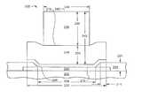
- FIG. 1PRIOR ART
- the integrated circuit package 100includes an integrated circuit 102 having input/output contact pads 104 under a passivation layer 106 .
- horizontalas used in herein is defined as a plane parallel to the conventional plane or under surface of the integrated circuit package, such as the integrated circuit package 100 , regardless of its orientation.
- verticalrefers to a direction perpendicular to the horizontal as just defined. Terms, such as “on”, “above”, “below”, “side”, “higher”, “lower”, “over”, and “under”, are defined with respect to the horizontal plane.
- processingas used herein includes deposition of material or photoresist, patterning, exposure, development, etching, cleaning, and/or removal of the material or photoresist as required in forming a described structure.
- the passivation layer 106has openings 108 provided therein which expose the input/output contact pads 104 .
- Under bump metallurgies (UBMs) 110line the openings 108 and extend distances 112 beyond the edges of the openings 108 . Where the openings 108 are rectangular, the UBMs 110 are rectangular.
- the bumps 114 for the UMBs 110will be of substantially rectangular block configurations; e.g., blocks with rounded corners and flat tops. Different configurations of the UMBs 110 are possible including cylindrical and cubical.
- the bumps 114do not have flat top surfaces which match with the flat surface of the lead tape (not shown) to which the bumps 114 are bonded.
- the UBM 110In order to protect the input/output contact pads 104 from corrosion, it is necessary that the UBM 110 must extend the distances 112 beyond the openings 108 . It has been discovered that the thicknesses of the passivation layer 106 in the distances 112 causes the top surfaces of the bumps 114 to have depressions 116 surrounded by rectangular ring structures 118 having ring thicknesses 120 .
- the ring thicknesses 120are about 5 um to about 10 um thick in a horizontal direction and about 1 um in a vertical direction. Since the thickness of the passivation layer 106 is about 1 um, the uniform bump plating causes the depression 116 to be around 1 urn deep. The depression 116 is extremely small, but it is believed that the rectangular ring structures 118 are sufficiently deep and large enough to entrap air in the depressions 116 between the bumps 114 the flat tape during TAB and sometimes prevent bonding and/or sometimes affect the electrical properties of the bond.
- the bumps 114 of the prior arthave widths 122 , heights 124 and are spaced apart a center-to-center distance 126 .
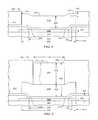
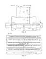
- the integrated circuit package 200includes an integrated circuit 202 having an input/output contact pad 204 under a passivation layer 206 .
- the input/output contact pad 204is of aluminum or an aluminum alloy under the passivation layer 206 of a dielectric material.
- the passivation layer 206is deposited to a thickness 207 and has an opening 208 provided therein which exposes the input/output contact pad 204 to define a contact area 209 .
- the contact area 209will have a contact width and contact length as dimensions.
- the opening 208is circular or square, the contact area 209 will have a diameter or a width as dimensions.
- the UMB 210includes a first layer of titanium-tungsten alloy or chrome and a second layer of gold, which are successively deposited on the contact area 209 and the passivation layer 206 by sputter deposition.
- FIG. 4therein is shown the structure of FIG. 3 after plating of a bump pad 214 .
- the bump pad 214is formed in a number of steps.
- a photoresist 213is deposited, patterned, and processed on the under bump metallurgy to form an opening 215 .
- the opening 215will extend beyond the perimeter of the opening 208 by a distance 212 to provide corrosion protection for the input/output contact pad 204 when applying the under bump metalurgy etching later.
- the opening 208is rectangular
- the opening 215is rectangular and has an outside dimension 222 .
- the bump pad 214is formed on the UMB 210 by plating in the opening 215 using the UMB 210 as a common ground.
- the bump pad 214is of a metal or metal alloy having a hardness in a critical range from 500 to 600 HV (Vickers Hardness), such as a nickel or nickel alloy.
- HVVanickers Hardness
- the thickness of the passivation layer 206 in the distance 212causes the top surface of the bump pad 214 to have an depression 216 surrounded by a rectangular ring structure 218 having a ring thicknesses 220 .
- the bump pad 214will have a cross-sectional area with a dimension 222 and a height 224 above the UBM 210 .
- the height 224will be less than the height 124 of FIG. 1 (PRIOR ART).
- FIG. 5therein is shown the structure of FIG. 4 after plating of a bump 230 .
- a photoresist 232has been deposited over the photoresist 213 of FIG. 4 and the bump pad 214 .
- the photoresist 232has been patterned and processed to form an opening 234 around the depression 216 of the bump pad 214 .
- the bump 230is of a metal or metal alloy having a hardness from 30 to 70 HV, such as a gold or gold alloy.
- the bump pad 214 of a material including nickel and the bump 230 of a material including goldhas been discovered to be that the softness and anti-corrosion resistance of the gold material allows for good wire bonding connections to gold or copper wire while at the same time, the hardness of the nickel material, which corrodes relatively easily, protects the silicon substrate of the integrated circuit 202 from being broken by the bonding or assembly process.
- the particular ranges of hardnesshave been found to be critical to optimize the balance between being sufficiently hard while being sufficiently soft to confer both good wire bonding and substrate protection.
- the bump 230can be deposited by a number of different methods including plating.
- the bump pad 214 and the bump 230can be of different materials to conserve cost or the same materials to improve electrical performance.
- the bump 230is gold deposited by plating to be compatible with the tape automated bonding (TAB) process, which requires the integrated circuit 200 to bond to a copper, gold, tin plated copper, or a copper/plastic laminated tape.
- TABtape automated bonding
- the bump 230has been plated into the opening 234 to have a cross-sectional area with a dimension 236 which is less than a dimension 209 and a height 238 over the UBM 210 so as to have an overall height of 240 .
- the overall height 240is same to the height 124 of FIG. 1 and greater than the height 224 .
- the top surface 242 of the bump 230will be flat within 0.5 um regardless of the thickness 207 of the passivation layer 206 .
- the term “flat”will mean a degree of flatness within 0.5 um. This means that the top surface 242 of the bump 230 will not have a depression so proper bonding will always occur and the electrical properties of the bond will be uniform despite size reductions in the technology and in the bump 230 .
- FIG. 6therein is shown the completed integrated circuit package 200 with the bump 230 in accordance with the present invention.
- the photoresist 232has been removed and UBM 210 has been etched to the size of the bump pad 214 .
- the method 300includes: a step 302 of forming a contact pad on an integrated circuit; a step 304 of forming a passivation layer on the integrated circuit; a step 306 of forming an opening in the passivation layer exposing the contact pad; a step 308 of forming an under bump metallurgy over the contact pad; a step 310 forming a bump pad over the under bump metallurgy; and a step 312 of forming a bump on and over the bump pad.
Landscapes
- Engineering & Computer Science (AREA)
- Computer Hardware Design (AREA)
- Microelectronics & Electronic Packaging (AREA)
- Power Engineering (AREA)
- Manufacturing & Machinery (AREA)
- Wire Bonding (AREA)
Abstract
Description
- This is a continuation-in-part of co-pending U.S. patent application Ser. No. 10/251,512 filed Sep. 19, 2002.
- The present invention relates generally to the fabrication of semiconductor integrated circuit packages, and more specifically to packages with metal bumps for making electrical connections.
- Electronic products have become an aspect of every day life from televisions to cell phones to wristwatches. The hearts of these electronic products are integrated circuits, which continue to be made smaller and more reliable while increasing performance and speed.
- An integrated circuit is typically packaged in a tiny box-type structure usually on the order of a few millimeters per side. The integrated circuit package generally has cylindrical terminals formed through a passivation layer of the integrated circuit near its edges for directly bonding the integrated circuit package to a foil-type lead frame that is usually less than 0.5 mm in thickness.
- The bonding technique is referred to as tape automated bonding or TAB. In the TAB process a lead tape is first prepared by etching electrical leads into it at positions corresponding to the locations of the cylindrical terminals on the integrated circuit package. The lead tape is then fed into an inner lead bonder, which is an apparatus equipped with a thermode (a heated instrument that presses the integrated circuit package and the tape together). The inner ends of the electrical leads are bonded to the cylindrical terminals on the integrated circuit package by compressing them together in the heated thermode in a single operation.
- The integrated circuit package and the bonded leads can then be excised out of the tape for connection to a circuit board, which goes into the electronic products.
- The cylindrical terminals on the integrated circuit are often called “gold bumps” because they are gold-plated and look like bumps protruding from the integrated circuit package. This structure is required because aluminum metallization is typically used for wiring inside integrated circuits so input/output contact pads under the passivation layer are typically aluminum or aluminum alloy.
- Aluminum and aluminum alloys are highly susceptible to corrosion if left exposed to the environment and, as a result, one or two protective passivation layers of silicon oxide, silicon nitride or polyimide are applied. Then an opening is formed by plasma or reactive ion etching in the passivation layers to expose the input/output contact pad. The thin film deposition is performed by evaporation or sputtering. The thin film layers deposited are called “under bump metallurgy” (UBM). UBM plays critical roles: as an adhesion layer between the aluminum metallization and the gold bumps; and as a common ground for the subsequent electroplating of the gold bump. Before plating, a photoresist layer is coated and developed to define the opening for bumps. The photoresist opening must have some overlap on both side of passivation opening to protect the aluminum input/output contact pad during UBM etching after plating because acid will be applied during etching. The overlap is from 6 um to 10 um depending on the exposure tools and process control. During plating, the plating rate is same at everywhere, so the final surface of gold bump is not flat because of the thickness of the passivation layers. At center area of the gold bump, the thickness is always lower, like the center of a ring. If the thickness of the passivation layers is less than 1 um, there is no any problem. But more products now require passivation layers, which are more than 1 um thick so the current technology is limited.
- A solution to this problem has been long sought but prior developments have not taught or suggested any solutions and, thus, a solution to this problem has long eluded those skilled in the art.
- The present invention provides a manufacturing method for an integrated circuit package including forming a contact pad under a passivation layer on an integrated circuit, forming an opening in the passivation layer exposing the contact pad, and forming an under bump metallurgy over the contact pad and the passivation layer. The method further includes forming a bump pad over the under bump metallurgy of a material having a first hardness and forming a bump on and over the bump pad, the bump having a top flat surface and of a material having a second hardness softer than the first hardness.
- The TAB using the bump technology of the present invention provides bonds that hold and have a flat surface and low resistance even with reductions in the size of the technology.
- Certain embodiments of the invention have other advantages in addition to or in place of those mentioned above. The advantages will become apparent to those skilled in the art from a reading of the following detailed description when taken with reference to the accompanying drawings.
FIG. 1 (PRIOR ART) is a cross-sectional view of prior art integrated circuit package;FIG. 2 is a close up view of an integrated circuit package with a contact pad in an intermediate stage of manufacture according to the present invention;FIG. 3 is the structure ofFIG. 2 after deposition of an under bump metallurgy;FIG. 4 is the structure ofFIG. 3 after plating of a bump pad;FIG. 5 is the structure ofFIG. 4 after plating of a bump;FIG. 6 is the completed integrated circuit package with a bump in accordance with the present invention; andFIG. 7 is a flowchart of a method for manufacturing an integrated circuit package with a gold bump in accordance with the present invention.- Referring now to
FIG. 1 (PRIOR ART), therein is shown a cross-sectional view of aintegrated circuit package 100 in the prior art. Theintegrated circuit package 100 includes anintegrated circuit 102 having input/output contact pads 104 under apassivation layer 106. - The term “horizontal” as used in herein is defined as a plane parallel to the conventional plane or under surface of the integrated circuit package, such as the
integrated circuit package 100, regardless of its orientation. The term “vertical” refers to a direction perpendicular to the horizontal as just defined. Terms, such as “on”, “above”, “below”, “side”, “higher”, “lower”, “over”, and “under”, are defined with respect to the horizontal plane. The term “processing” as used herein includes deposition of material or photoresist, patterning, exposure, development, etching, cleaning, and/or removal of the material or photoresist as required in forming a described structure. - The
passivation layer 106 hasopenings 108 provided therein which expose the input/output contact pads 104. Under bump metallurgies (UBMs)110 line theopenings 108 and extenddistances 112 beyond the edges of theopenings 108. Where theopenings 108 are rectangular, theUBMs 110 are rectangular. Bumps 114 are deposited on theUBMs 110 by a plating process. Thebumps 114 for the UMBs110 will be of substantially rectangular block configurations; e.g., blocks with rounded corners and flat tops. Different configurations of theUMBs 110 are possible including cylindrical and cubical.- It has been unexpectedly discovered, while investigating the problems of poor bonding and poor electrical connection using the
bumps 114, that thebumps 114 do not have flat top surfaces which match with the flat surface of the lead tape (not shown) to which thebumps 114 are bonded. - In order to protect the input/
output contact pads 104 from corrosion, it is necessary that theUBM 110 must extend thedistances 112 beyond theopenings 108. It has been discovered that the thicknesses of thepassivation layer 106 in thedistances 112 causes the top surfaces of thebumps 114 to havedepressions 116 surrounded byrectangular ring structures 118 havingring thicknesses 120. - In some embodiments, the
ring thicknesses 120 are about 5 um to about 10 um thick in a horizontal direction and about 1 um in a vertical direction. Since the thickness of thepassivation layer 106 is about 1 um, the uniform bump plating causes thedepression 116 to be around1 urn deep. Thedepression 116 is extremely small, but it is believed that therectangular ring structures 118 are sufficiently deep and large enough to entrap air in thedepressions 116 between thebumps 114 the flat tape during TAB and sometimes prevent bonding and/or sometimes affect the electrical properties of the bond. - The
bumps 114 of the prior art havewidths 122,heights 124 and are spaced apart a center-to-center distance 126. - Referring now to
FIG. 2 , therein is shown a close up view of anintegrated circuit package 200 in an intermediate stage of manufacture according to the present invention. Theintegrated circuit package 200 includes anintegrated circuit 202 having an input/output contact pad 204 under apassivation layer 206. In one embodiment, the input/output contact pad 204 is of aluminum or an aluminum alloy under thepassivation layer 206 of a dielectric material. - The
passivation layer 206 is deposited to athickness 207 and has anopening 208 provided therein which exposes the input/output contact pad 204 to define acontact area 209. Where theopening 208 is rectangular, thecontact area 209 will have a contact width and contact length as dimensions. Where theopening 208 is circular or square, thecontact area 209 will have a diameter or a width as dimensions. - Referring now to
FIG. 3 , therein is shown the structure ofFIG. 2 after deposition of an under bump metallurgy (UBM)210. In one embodiment of the present invention, theUMB 210 includes a first layer of titanium-tungsten alloy or chrome and a second layer of gold, which are successively deposited on thecontact area 209 and thepassivation layer 206 by sputter deposition. - Referring now to
FIG. 4 , therein is shown the structure ofFIG. 3 after plating of abump pad 214. Thebump pad 214 is formed in a number of steps. - A
photoresist 213 is deposited, patterned, and processed on the under bump metallurgy to form anopening 215. Theopening 215 will extend beyond the perimeter of theopening 208 by adistance 212 to provide corrosion protection for the input/output contact pad 204 when applying the under bump metalurgy etching later. Where theopening 208 is rectangular, theopening 215 is rectangular and has anoutside dimension 222. Thebump pad 214 is formed on theUMB 210 by plating in theopening 215 using theUMB 210 as a common ground. - It has been unexpectedly discovered that it is particularly advantageous when the
bump pad 214 is of a metal or metal alloy having a hardness in a critical range from 500 to 600 HV (Vickers Hardness), such as a nickel or nickel alloy. The full extent of the discovery will be discussed below. - It will be noted that the thickness of the
passivation layer 206 in thedistance 212 causes the top surface of thebump pad 214 to have andepression 216 surrounded by arectangular ring structure 218 having a ring thicknesses220. - The
bump pad 214 will have a cross-sectional area with adimension 222 and aheight 224 above theUBM 210. Theheight 224 will be less than theheight 124 ofFIG. 1 (PRIOR ART). - Referring now to
FIG. 5 , therein is shown the structure ofFIG. 4 after plating of abump 230. - In one embodiment, a
photoresist 232 has been deposited over thephotoresist 213 ofFIG. 4 and thebump pad 214. Thephotoresist 232 has been patterned and processed to form anopening 234 around thedepression 216 of thebump pad 214. - It has been unexpectedly discovered that it is particularly advantageous when the
bump 230 is of a metal or metal alloy having a hardness from 30 to 70 HV, such as a gold or gold alloy. - As explained above, it is unexpectedly advantageous to have the
bump pad 214 of a material including nickel and thebump 230 of a material including gold. The reason for this synergy has been discovered to be that the softness and anti-corrosion resistance of the gold material allows for good wire bonding connections to gold or copper wire while at the same time, the hardness of the nickel material, which corrodes relatively easily, protects the silicon substrate of theintegrated circuit 202 from being broken by the bonding or assembly process. The particular ranges of hardness have been found to be critical to optimize the balance between being sufficiently hard while being sufficiently soft to confer both good wire bonding and substrate protection. - The
bump 230 can be deposited by a number of different methods including plating. Thebump pad 214 and thebump 230 can be of different materials to conserve cost or the same materials to improve electrical performance. In one embodiment, thebump 230 is gold deposited by plating to be compatible with the tape automated bonding (TAB) process, which requires theintegrated circuit 200 to bond to a copper, gold, tin plated copper, or a copper/plastic laminated tape. - The
bump 230 has been plated into theopening 234 to have a cross-sectional area with adimension 236 which is less than adimension 209 and aheight 238 over theUBM 210 so as to have an overall height of240. In one embodiment, theoverall height 240 is same to theheight 124 ofFIG. 1 and greater than theheight 224. - Since the bottom of the
depression 216 is flat within 0.5 um, thetop surface 242 of thebump 230 will be flat within 0.5 um regardless of thethickness 207 of thepassivation layer 206. As used herein, the term “flat” will mean a degree of flatness within 0.5 um. This means that thetop surface 242 of thebump 230 will not have a depression so proper bonding will always occur and the electrical properties of the bond will be uniform despite size reductions in the technology and in thebump 230. - Referring now to
FIG. 6 , therein is shown the completedintegrated circuit package 200 with thebump 230 in accordance with the present invention. Thephotoresist 232 has been removed andUBM 210 has been etched to the size of thebump pad 214. - Referring now to
FIG. 7 therein is shown a flowchart of amethod 300 for manufacturing an integrated circuit package with a bump in accordance with the present invention. Themethod 300 includes: astep 302 of forming a contact pad on an integrated circuit; astep 304 of forming a passivation layer on the integrated circuit; astep 306 of forming an opening in the passivation layer exposing the contact pad; astep 308 of forming an under bump metallurgy over the contact pad; astep 310 forming a bump pad over the under bump metallurgy; and astep 312 of forming a bump on and over the bump pad. - While the invention has been described in conjunction with a specific best mode, it is to be understood that many alternatives, modifications, and variations will be apparent to those skilled in the art in light of the aforegoing description. Accordingly, it is intended to embrace all such alternatives, modifications, and variations that fall within the spirit and scope of the included claims. All matters hither-to-fore set forth or shown in the accompanying drawings are to be interpreted in an illustrative and non-limiting sense.
Claims (20)
Priority Applications (2)
| Application Number | Priority Date | Filing Date | Title |
|---|---|---|---|
| US10/908,254US20050242446A1 (en) | 2002-09-19 | 2005-05-04 | Integrated circuit package with different hardness bump pad and bump and manufacturing method therefor |
| SG200508485ASG126814A1 (en) | 2005-05-04 | 2005-10-31 | Integrated circuit package with different hardnes s bump pad and bump and manufacturing method therefor |
Applications Claiming Priority (2)
| Application Number | Priority Date | Filing Date | Title |
|---|---|---|---|
| US10/251,512US20040222520A1 (en) | 2002-09-19 | 2002-09-19 | Integrated circuit package with flat metal bump and manufacturing method therefor |
| US10/908,254US20050242446A1 (en) | 2002-09-19 | 2005-05-04 | Integrated circuit package with different hardness bump pad and bump and manufacturing method therefor |
Related Parent Applications (1)
| Application Number | Title | Priority Date | Filing Date |
|---|---|---|---|
| US10/251,512Continuation-In-PartUS20040222520A1 (en) | 2002-09-19 | 2002-09-19 | Integrated circuit package with flat metal bump and manufacturing method therefor |
Publications (1)
| Publication Number | Publication Date |
|---|---|
| US20050242446A1true US20050242446A1 (en) | 2005-11-03 |
Family
ID=46205573
Family Applications (1)
| Application Number | Title | Priority Date | Filing Date |
|---|---|---|---|
| US10/908,254AbandonedUS20050242446A1 (en) | 2002-09-19 | 2005-05-04 | Integrated circuit package with different hardness bump pad and bump and manufacturing method therefor |
Country Status (1)
| Country | Link |
|---|---|
| US (1) | US20050242446A1 (en) |
Cited By (13)
| Publication number | Priority date | Publication date | Assignee | Title |
|---|---|---|---|---|
| US20050054187A1 (en)* | 2003-09-05 | 2005-03-10 | Advanced Semiconductor Engineering, Inc. | Method for forming ball pads of BGA substrate |
| US20060189114A1 (en)* | 2005-02-23 | 2006-08-24 | Kabushiki Kaisha Toshiba | Method of manufacturing semiconductor device and semiconductor device |
| US20070052110A1 (en)* | 2005-09-07 | 2007-03-08 | Su-Tsai Lu | Chip structure, chip package structure and bumping process thereof |
| US20070235873A1 (en)* | 2006-03-28 | 2007-10-11 | Cheng Hsu M | Pad structures and methods for forming pad structures |
| US20090079082A1 (en)* | 2007-09-24 | 2009-03-26 | Yong Liu | Bonding pad structure allowing wire bonding over an active area in a semiconductor die and method of manufacturing same |
| US20100200969A1 (en)* | 2009-02-09 | 2010-08-12 | Advanced Semiconductor Engineering, Inc. | Semiconductor package and method of manufacturing the same |
| US20130292819A1 (en)* | 2012-05-07 | 2013-11-07 | Novatek Microelectronics Corp. | Chip-on-film device |
| US8618677B2 (en) | 2012-04-06 | 2013-12-31 | Advanced Semiconductor Engineering, Inc. | Wirebonded semiconductor package |
| TWI467719B (en)* | 2012-05-07 | 2015-01-01 | Novatek Microelectronics Corp | Chip-on-film device |
| KR101495713B1 (en)* | 2012-05-07 | 2015-02-25 | 노바텍 마이크로일렉트로닉스 코포레이션 | Chip-on-film device |
| US10438916B2 (en)* | 2016-04-01 | 2019-10-08 | Intel Corporation | Wire bond connection with intermediate contact structure |
| US10755995B2 (en)* | 2018-06-28 | 2020-08-25 | Taiwan Semiconductor Manufacturing Co., Ltd. | Warpage control of semiconductor die |
| CN112951784A (en)* | 2019-12-11 | 2021-06-11 | 长鑫存储技术有限公司 | Wire bonding structure, wire bonding method, and semiconductor device |
Citations (6)
| Publication number | Priority date | Publication date | Assignee | Title |
|---|---|---|---|---|
| US5310699A (en)* | 1984-08-28 | 1994-05-10 | Sharp Kabushiki Kaisha | Method of manufacturing a bump electrode |
| US5783868A (en)* | 1996-09-20 | 1998-07-21 | Integrated Device Technology, Inc. | Extended bond pads with a plurality of perforations |
| US6417089B1 (en)* | 2000-01-03 | 2002-07-09 | Samsung Electronics, Co., Ltd. | Method of forming solder bumps with reduced undercutting of under bump metallurgy (UBM) |
| US6448171B1 (en)* | 2000-05-05 | 2002-09-10 | Aptos Corporation | Microelectronic fabrication having formed therein terminal electrode structure providing enhanced passivation and enhanced bondability |
| US20020192939A1 (en)* | 1999-12-27 | 2002-12-19 | Hoya Corporation | Method of manufacturing a contract element and a multi-layered wiring substrate, and wafer batch contact board |
| US20030129822A1 (en)* | 2002-01-07 | 2003-07-10 | Jin-Yuan Lee | Cylindrical bonding structure and method of manufacture |
- 2005
- 2005-05-04USUS10/908,254patent/US20050242446A1/ennot_activeAbandoned
Patent Citations (7)
| Publication number | Priority date | Publication date | Assignee | Title |
|---|---|---|---|---|
| US5310699A (en)* | 1984-08-28 | 1994-05-10 | Sharp Kabushiki Kaisha | Method of manufacturing a bump electrode |
| US5783868A (en)* | 1996-09-20 | 1998-07-21 | Integrated Device Technology, Inc. | Extended bond pads with a plurality of perforations |
| US20020192939A1 (en)* | 1999-12-27 | 2002-12-19 | Hoya Corporation | Method of manufacturing a contract element and a multi-layered wiring substrate, and wafer batch contact board |
| US6417089B1 (en)* | 2000-01-03 | 2002-07-09 | Samsung Electronics, Co., Ltd. | Method of forming solder bumps with reduced undercutting of under bump metallurgy (UBM) |
| US6448171B1 (en)* | 2000-05-05 | 2002-09-10 | Aptos Corporation | Microelectronic fabrication having formed therein terminal electrode structure providing enhanced passivation and enhanced bondability |
| US20030129822A1 (en)* | 2002-01-07 | 2003-07-10 | Jin-Yuan Lee | Cylindrical bonding structure and method of manufacture |
| US20030127734A1 (en)* | 2002-01-07 | 2003-07-10 | Jin-Yuan Lee | Cylindrical bonding structure and method of manufacture |
Cited By (21)
| Publication number | Priority date | Publication date | Assignee | Title |
|---|---|---|---|---|
| US20050054187A1 (en)* | 2003-09-05 | 2005-03-10 | Advanced Semiconductor Engineering, Inc. | Method for forming ball pads of BGA substrate |
| US20060189114A1 (en)* | 2005-02-23 | 2006-08-24 | Kabushiki Kaisha Toshiba | Method of manufacturing semiconductor device and semiconductor device |
| US7473628B2 (en)* | 2005-02-23 | 2009-01-06 | Kabushiki Kaisha Toshiba | Method of manufacturing semiconductor device and semiconductor device |
| US20090134516A1 (en)* | 2005-02-23 | 2009-05-28 | Kabushiki Kaisha Toshiba, | Method of manufacturing semiconductor device and semiconductor device |
| US20070052110A1 (en)* | 2005-09-07 | 2007-03-08 | Su-Tsai Lu | Chip structure, chip package structure and bumping process thereof |
| US7423348B2 (en)* | 2005-09-07 | 2008-09-09 | Industrial Technology Research Institute | Chip structure and chip package structure |
| US20070235873A1 (en)* | 2006-03-28 | 2007-10-11 | Cheng Hsu M | Pad structures and methods for forming pad structures |
| US7759776B2 (en) | 2006-03-28 | 2010-07-20 | Taiwan Semiconductor Manufacturing Co., Ltd. | Space transformer having multi-layer pad structures |
| US20090079082A1 (en)* | 2007-09-24 | 2009-03-26 | Yong Liu | Bonding pad structure allowing wire bonding over an active area in a semiconductor die and method of manufacturing same |
| US8357998B2 (en) | 2009-02-09 | 2013-01-22 | Advanced Semiconductor Engineering, Inc. | Wirebonded semiconductor package |
| US20100200969A1 (en)* | 2009-02-09 | 2010-08-12 | Advanced Semiconductor Engineering, Inc. | Semiconductor package and method of manufacturing the same |
| US8618677B2 (en) | 2012-04-06 | 2013-12-31 | Advanced Semiconductor Engineering, Inc. | Wirebonded semiconductor package |
| US20130292819A1 (en)* | 2012-05-07 | 2013-11-07 | Novatek Microelectronics Corp. | Chip-on-film device |
| TWI467719B (en)* | 2012-05-07 | 2015-01-01 | Novatek Microelectronics Corp | Chip-on-film device |
| KR101495713B1 (en)* | 2012-05-07 | 2015-02-25 | 노바텍 마이크로일렉트로닉스 코포레이션 | Chip-on-film device |
| US20150069602A1 (en)* | 2012-05-07 | 2015-03-12 | Novatek Microelectronics Corp. | Chip-on-film device |
| US10438916B2 (en)* | 2016-04-01 | 2019-10-08 | Intel Corporation | Wire bond connection with intermediate contact structure |
| US10755995B2 (en)* | 2018-06-28 | 2020-08-25 | Taiwan Semiconductor Manufacturing Co., Ltd. | Warpage control of semiconductor die |
| US11450584B2 (en) | 2018-06-28 | 2022-09-20 | Taiwan Semiconductor Manufacturing Co., Ltd. | Warpage control of semiconductor die |
| US12021002B2 (en) | 2018-06-28 | 2024-06-25 | Taiwan Semiconductor Manufacturing Co., Ltd. | Warpage control of semiconductor die |
| CN112951784A (en)* | 2019-12-11 | 2021-06-11 | 长鑫存储技术有限公司 | Wire bonding structure, wire bonding method, and semiconductor device |
Similar Documents
| Publication | Publication Date | Title |
|---|---|---|
| US7682960B2 (en) | Method of fabricating a wafer structure having a pad and a first protection layer and a second protection layer | |
| USRE48420E1 (en) | Method for fabricating low resistance, low inductance interconnections in high current semiconductor devices | |
| US7867826B2 (en) | Semiconductor device packaged into chip size and manufacturing method thereof | |
| US8785317B2 (en) | Wafer level packaging of semiconductor chips | |
| US5631499A (en) | Semiconductor device comprising fine bump electrode having small side etch portion and stable characteristics | |
| US20070145603A1 (en) | Semiconductor chip, mounting structure thereof, and methods for forming a semiconductor chip and printed circuit board for the mounting structure thereof | |
| US20070224798A1 (en) | Semiconductor device and medium of fabricating the same | |
| USRE48421E1 (en) | Flip chip and method of making flip chip | |
| US20050242446A1 (en) | Integrated circuit package with different hardness bump pad and bump and manufacturing method therefor | |
| US20040222520A1 (en) | Integrated circuit package with flat metal bump and manufacturing method therefor | |
| US7381636B2 (en) | Planar bond pad design and method of making the same | |
| US7217656B2 (en) | Structure and method for bond pads of copper-metallized integrated circuits | |
| USRE48422E1 (en) | Method of making flip chip | |
| JP2005123247A (en) | Semiconductor device and manufacturing method thereof | |
| US20030189249A1 (en) | Chip structure and wire bonding process suited for the same | |
| US20070085224A1 (en) | Semiconductor device having strong adhesion between wiring and protective film, and manufacturing method therefor | |
| KR100620911B1 (en) | Gold bump manufacturing method of semiconductor device | |
| US11705399B2 (en) | Terminal configuration and semiconductor device | |
| CN118366872B (en) | Preparation method of fan-out type packaging structure and fan-out type packaging structure | |
| US20040115942A1 (en) | Bonding pad of a semiconductor device and formation method thereof | |
| JP3213923B2 (en) | Underbarrier metal ribbon for bump formation and bump formation method | |
| TW200522307A (en) | Semiconductor device and method of manufacturing thereof, circuit board, and electronic apparatus | |
| JPH03132036A (en) | Manufacturing method of semiconductor device | |
| JPH02244722A (en) | Forming method for bump electrode of semiconductor element | |
| WO2004105132A1 (en) | An electrical connection for a microelectronic chip, and a method for manufacturing such a connection |
Legal Events
| Date | Code | Title | Description |
|---|---|---|---|
| AS | Assignment | Owner name:STATS CHIPPAC LTD., SINGAPORE Free format text:ASSIGNMENT OF ASSIGNORS INTEREST;ASSIGNOR:JIN, YONGGANG;REEL/FRAME:016848/0509 Effective date:20050714 | |
| STCB | Information on status: application discontinuation | Free format text:ABANDONED -- FAILURE TO RESPOND TO AN OFFICE ACTION | |
| AS | Assignment | Owner name:CITICORP INTERNATIONAL LIMITED, AS COMMON SECURITY AGENT, HONG KONG Free format text:SECURITY INTEREST;ASSIGNORS:STATS CHIPPAC, INC.;STATS CHIPPAC LTD.;REEL/FRAME:036288/0748 Effective date:20150806 Owner name:CITICORP INTERNATIONAL LIMITED, AS COMMON SECURITY Free format text:SECURITY INTEREST;ASSIGNORS:STATS CHIPPAC, INC.;STATS CHIPPAC LTD.;REEL/FRAME:036288/0748 Effective date:20150806 | |
| AS | Assignment | Owner name:STATS CHIPPAC PTE. LTE., SINGAPORE Free format text:CHANGE OF NAME;ASSIGNOR:STATS CHIPPAC LD.;REEL/FRAME:038378/0442 Effective date:20160329 | |
| AS | Assignment | Owner name:STATS CHIPPAC PTE. LTE., SINGAPORE Free format text:CORRECTIVE ASSIGNMENT TO CORRECT THE ASSIGNOR'S NAME PREVIOUSLY RECORDED ON REEL 038378 FRAME 0442. ASSIGNOR(S) HEREBY CONFIRMS THE CHANGE OF NAME;ASSIGNOR:STATS CHIPPAC LTD.;REEL/FRAME:039514/0451 Effective date:20160329 | |
| AS | Assignment | Owner name:STATS CHIPPAC PTE. LTD., SINGAPORE Free format text:CORRECTIVE ASSIGNMENT TO CORRECT THE ASSIGNOR NAME PREVIOUSLY RECORDED AT REEL: 039514 FRAME: 0451. ASSIGNOR(S) HEREBY CONFIRMS THE CHANGE OF NAME;ASSIGNOR:STATS CHIPPAC LTD.;REEL/FRAME:039980/0838 Effective date:20160329 | |
| AS | Assignment | Owner name:STATS CHIPPAC PTE. LTD. FORMERLY KNOWN AS STATS CHIPPAC LTD., SINGAPORE Free format text:RELEASE BY SECURED PARTY;ASSIGNOR:CITICORP INTERNATIONAL LIMITED, AS COMMON SECURITY AGENT;REEL/FRAME:053476/0094 Effective date:20190503 Owner name:STATS CHIPPAC, INC., CALIFORNIA Free format text:RELEASE BY SECURED PARTY;ASSIGNOR:CITICORP INTERNATIONAL LIMITED, AS COMMON SECURITY AGENT;REEL/FRAME:053476/0094 Effective date:20190503 |