US20050242348A1 - Thin film transistor and organic electroluminescence display using the same - Google Patents
Thin film transistor and organic electroluminescence display using the sameDownload PDFInfo
- Publication number
- US20050242348A1 US20050242348A1US11/095,601US9560105AUS2005242348A1US 20050242348 A1US20050242348 A1US 20050242348A1US 9560105 AUS9560105 AUS 9560105AUS 2005242348 A1US2005242348 A1US 2005242348A1
- Authority
- US
- United States
- Prior art keywords
- region
- display
- electrode
- layer
- drain
- Prior art date
- Legal status (The legal status is an assumption and is not a legal conclusion. Google has not performed a legal analysis and makes no representation as to the accuracy of the status listed.)
- Granted
Links
Images


Classifications
- H—ELECTRICITY
- H05—ELECTRIC TECHNIQUES NOT OTHERWISE PROVIDED FOR
- H05B—ELECTRIC HEATING; ELECTRIC LIGHT SOURCES NOT OTHERWISE PROVIDED FOR; CIRCUIT ARRANGEMENTS FOR ELECTRIC LIGHT SOURCES, IN GENERAL
- H05B33/00—Electroluminescent light sources
- H—ELECTRICITY
- H10—SEMICONDUCTOR DEVICES; ELECTRIC SOLID-STATE DEVICES NOT OTHERWISE PROVIDED FOR
- H10D—INORGANIC ELECTRIC SEMICONDUCTOR DEVICES
- H10D30/00—Field-effect transistors [FET]
- H10D30/01—Manufacture or treatment
- H10D30/021—Manufacture or treatment of FETs having insulated gates [IGFET]
- H10D30/031—Manufacture or treatment of FETs having insulated gates [IGFET] of thin-film transistors [TFT]
- H10D30/0312—Manufacture or treatment of FETs having insulated gates [IGFET] of thin-film transistors [TFT] characterised by the gate electrodes
- H10D30/0314—Manufacture or treatment of FETs having insulated gates [IGFET] of thin-film transistors [TFT] characterised by the gate electrodes of lateral top-gate TFTs comprising only a single gate
- H—ELECTRICITY
- H10—SEMICONDUCTOR DEVICES; ELECTRIC SOLID-STATE DEVICES NOT OTHERWISE PROVIDED FOR
- H10D—INORGANIC ELECTRIC SEMICONDUCTOR DEVICES
- H10D30/00—Field-effect transistors [FET]
- H10D30/01—Manufacture or treatment
- H10D30/021—Manufacture or treatment of FETs having insulated gates [IGFET]
- H10D30/031—Manufacture or treatment of FETs having insulated gates [IGFET] of thin-film transistors [TFT]
- H10D30/0321—Manufacture or treatment of FETs having insulated gates [IGFET] of thin-film transistors [TFT] comprising silicon, e.g. amorphous silicon or polysilicon
- H—ELECTRICITY
- H10—SEMICONDUCTOR DEVICES; ELECTRIC SOLID-STATE DEVICES NOT OTHERWISE PROVIDED FOR
- H10D—INORGANIC ELECTRIC SEMICONDUCTOR DEVICES
- H10D30/00—Field-effect transistors [FET]
- H10D30/60—Insulated-gate field-effect transistors [IGFET]
- H10D30/67—Thin-film transistors [TFT]
- H10D30/6704—Thin-film transistors [TFT] having supplementary regions or layers in the thin films or in the insulated bulk substrates for controlling properties of the device
- H10D30/6713—Thin-film transistors [TFT] having supplementary regions or layers in the thin films or in the insulated bulk substrates for controlling properties of the device characterised by the properties of the source or drain regions, e.g. compositions or sectional shapes
- H10D30/6715—Thin-film transistors [TFT] having supplementary regions or layers in the thin films or in the insulated bulk substrates for controlling properties of the device characterised by the properties of the source or drain regions, e.g. compositions or sectional shapes characterised by the doping profiles, e.g. having lightly-doped source or drain extensions
- H—ELECTRICITY
- H10—SEMICONDUCTOR DEVICES; ELECTRIC SOLID-STATE DEVICES NOT OTHERWISE PROVIDED FOR
- H10D—INORGANIC ELECTRIC SEMICONDUCTOR DEVICES
- H10D30/00—Field-effect transistors [FET]
- H10D30/60—Insulated-gate field-effect transistors [IGFET]
- H10D30/67—Thin-film transistors [TFT]
- H10D30/6729—Thin-film transistors [TFT] characterised by the electrodes
- H10D30/673—Thin-film transistors [TFT] characterised by the electrodes characterised by the shapes, relative sizes or dispositions of the gate electrodes
- H10D30/6731—Top-gate only TFTs
- H—ELECTRICITY
- H10—SEMICONDUCTOR DEVICES; ELECTRIC SOLID-STATE DEVICES NOT OTHERWISE PROVIDED FOR
- H10D—INORGANIC ELECTRIC SEMICONDUCTOR DEVICES
- H10D30/00—Field-effect transistors [FET]
- H10D30/60—Insulated-gate field-effect transistors [IGFET]
- H10D30/67—Thin-film transistors [TFT]
- H10D30/674—Thin-film transistors [TFT] characterised by the active materials
- H10D30/6741—Group IV materials, e.g. germanium or silicon carbide
- H10D30/6743—Silicon
- H10D30/6745—Polycrystalline or microcrystalline silicon
- H—ELECTRICITY
- H10—SEMICONDUCTOR DEVICES; ELECTRIC SOLID-STATE DEVICES NOT OTHERWISE PROVIDED FOR
- H10D—INORGANIC ELECTRIC SEMICONDUCTOR DEVICES
- H10D62/00—Semiconductor bodies, or regions thereof, of devices having potential barriers
- H10D62/40—Crystalline structures
- H—ELECTRICITY
- H10—SEMICONDUCTOR DEVICES; ELECTRIC SOLID-STATE DEVICES NOT OTHERWISE PROVIDED FOR
- H10K—ORGANIC ELECTRIC SOLID-STATE DEVICES
- H10K59/00—Integrated devices, or assemblies of multiple devices, comprising at least one organic light-emitting element covered by group H10K50/00
- H10K59/10—OLED displays
- H10K59/12—Active-matrix OLED [AMOLED] displays
- H10K59/121—Active-matrix OLED [AMOLED] displays characterised by the geometry or disposition of pixel elements
- H10K59/1213—Active-matrix OLED [AMOLED] displays characterised by the geometry or disposition of pixel elements the pixel elements being TFTs
- H—ELECTRICITY
- H10—SEMICONDUCTOR DEVICES; ELECTRIC SOLID-STATE DEVICES NOT OTHERWISE PROVIDED FOR
- H10K—ORGANIC ELECTRIC SOLID-STATE DEVICES
- H10K59/00—Integrated devices, or assemblies of multiple devices, comprising at least one organic light-emitting element covered by group H10K50/00
- H10K59/10—OLED displays
- H10K59/12—Active-matrix OLED [AMOLED] displays
- H10K59/123—Connection of the pixel electrodes to the thin film transistors [TFT]
Definitions
- the present inventionrelates to a thin film transistor (TFT) and an electroluminescence display using the same and, more particularly, to a TFT having a lightly doped drain (LDD) structure and an organic electroluminescence display using the same.
- TFTthin film transistor
- LDDlightly doped drain
- a pixel driving TFTmay be formed in each pixel to drive the pixel, and a TFT may be used in a driving circuit that drives the pixel driving TFT and applies a signal to a scan line (i.e., gate line) and a signal line (i.e., data line).
- a scan linei.e., gate line
- a signal linei.e., data line
- a polycrystalline silicon TFTmay be fabricated at a temperature similar to an amorphous silicon TFT, and it may have higher electron or hole mobility compared to the amorphous silicon TFT. Additionally, it may be possible to implement a complementary metal-oxide semiconductor (CMOS) TFT having an n-channel and a p-channel so that the driving circuit TFT and the pixel driving TFT may be simultaneously formed on a large-sized insulating substrate.
- CMOScomplementary metal-oxide semiconductor
- phosphorus (P)is typically used as a doping ion, and because phosphorus has mass relatively larger than that of boron (B), which is typically used for fabricating a PMOS TFT, silicon crystal may be destroyed, resulting in a damaged region. The damaged region may not be fully recovered even in subsequent activation processes.
- This damaged regionmay cause hot carrier stress, in which electrons may penetrate a gate insulating layer or a MOS interface when they accelerate from a source region to a drain region. Furthermore, the hot carrier stress may reduce electron mobility, which adversely affects stability of circuit operation in the organic electroluminescence display, and may increase an off current.
- LDDlightly doped drain
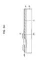
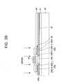
- FIG. 1A , FIG. 1B and FIG. 1Care cross-sectional views showing a TFT with a conventional LDD structure.
- a polycrystalline silicon (poly-Si) layermay be formed by depositing and crystallizing amorphous silicon on an insulating substrate 10 having a buffer layer 11 using plasma enhanced chemical vapor deposition (PECVD), low pressure chemical vapor deposition (LPCVD), sputtering, or other like methods.
- PECVDplasma enhanced chemical vapor deposition
- LPCVDlow pressure chemical vapor deposition
- sputteringor other like methods.
- photoresistmay then be formed on it to form an active layer, and an active layer 12 may be formed by patterning the poly-Si layer using the photoresist as a mask.
- a gate insulating layer 13may then be deposited on the active layer 12 , and a gate metal may be deposited on the gate insulating layer 13 .
- a gate electrode 14may then be formed by patterning the gate metal.
- low concentration dopingmay be carried out using the gate electrode 14 as a mask to form an LDD region in the active layer, thus defining source and drain regions 12 S and 12 D.
- a region between the source and drain regions 12 S and 12 Dacts as a channel region 12 C of the TFT.
- a photoresist pattern 15for forming the source and drain regions 12 S and 12 D having the LDD region of the TFT, may be formed by applying and exposing photoresist on the insulating substrate 10 .
- LDD regions 12 S-L and 12 D-L and highly doped regions 12 S-H and 12 D-Hmay be formed by performing high concentration doping into the active layer using the photoresist pattern 15 as a mask.
- contact holes 16 awhich expose a portion of the source and drain regions 12 S and 12 D, may be formed by forming and patterning an interlayer insulating layer 16 on an entire surface of the insulating substrate 10 having the gate electrode 14 .
- a conductive layermay be deposited on the entire surface of the insulating substrate 10 and be subjected to photolithography to form source and drain electrodes 17 S and 17 D, which are electrically connected to the source and drain regions 12 S and 12 D via the contact holes 16 a, thereby forming the TFT.
- the present inventionprovides a TFT having an LDD structure, and an organic electroluminescence display using the same, that may be formed without using a separate mask.
- the present inventiondiscloses a TFT comprising a lightly doped drain (LDD) region formation pattern and an active layer formed in an uneven structure on the LDD region formation pattern, and having a source region and a drain region including an LDD region
- LDDlightly doped drain
- the present inventionalso discloses a display comprising a lightly doped drain (LDD) region formation pattern and a pixel electrode formed on a same layer on an insulating substrate, an active layer formed in an uneven structure on the LDD region formation pattern, and having a source region and a drain region including an LDD region, a gate electrode formed on a gate insulating layer, and a source electrode and a drain electrode coupled to the source and drain regions, respectively. Either the source electrode or the drain electrode is coupled to the pixel electrode.
- LDDlightly doped drain
- the present inventionalso discloses a TFT comprising a source electrode and a drain electrode formed on an insulating substrate, and an active layer formed in an uneven structure on the source electrode and the drain electrodes and having a source region and a drain region including an LDD region.
- the present inventionalso discloses a display comprising a source electrode, a drain electrode, and a pixel electrode formed on a same layer on an insulating substrate, and an active layer having a source region and a drain region including an LDD region, and formed in an uneven structure on the source and drain electrodes.
- a gate insulating layeris formed on an entire surface of the insulating substrate having the active layer, and a gate electrode is formed on the gate insulating layer.
- An insulating layeris formed on an entire surface of the insulating substrate having the gate electrode, and it has an opening that defines an emission region by exposing a portion of the pixel electrode.
- An organic layeris formed on the opening of the insulating layer, and an upper electrode is formed on an entire surface of the insulating substrate.
- FIG. 1A , FIG. 1B and FIG. 1Care cross-sectional views showing a manufacturing process of a TFT having a conventional LDD structure.
- FIG. 2A , FIG. 2B , FIG. 2C and FIG. 2Dare cross-sectional views showing a manufacturing process of an organic electroluminescence display according to a first exemplary embodiment of the present invention.
- FIG. 3A , FIG. 3B and FIG. 3Care cross-sectional views showing a manufacturing process of an organic electroluminescence display according to a second exemplary embodiment of the present invention.
- FIG. 2A , FIG. 2B , FIG. 2C and FIG. 2Dare cross-sectional views showing a manufacturing process of an organic electroluminescence display according to a first exemplary embodiment of the present invention.
- a buffer layer 21(or, diffusion barrier) may be deposited on an insulating substrate 20 by PECVD, LPCVD, sputtering, or other like methods.
- the buffer layer 21may prevent insulating substrate impurities, such as metal ions, from diffusing and penetrating a poly-Si active layer.
- a glass or plastic substratemay be used as the insulating substrate 20 , glass is preferable.
- a pixel electrode 31 and an LDD region formation pattern 22may be formed on the buffer layer 21 by depositing and patterning a transparent conductive material, such as ITO, IZO or other like materials.
- Edge portions of the pixel electrode 31 and the LDD region formation pattern 22may have a taper angle of about 10° to about 45°.
- an amorphous silicon layermay be deposited on an entire surface of the insulating substrate by PECVD, LPCVD, sputtering, or other like methods.
- the amorphous silicon layermay be unevenly formed along the shape of the LDD region formation pattern 22 because the amorphous silicon layer on the edge portion of the LDD region formation pattern 22 may be formed along the edge portion's taper angle.
- a dehydrogenation processmay be carried out in a vacuum furnace after forming the amorphous silicon layer.
- the dehydrogenation processmay not be carried out when the amorphous silicon layer is deposited by the LPCVD or sputtering method.
- a poly-Si layermay be formed by crystallizing the amorphous silicon layer through an amorphous silicon crystallization process in which high energy is irradiated to the amorphous silicon layer.
- a crystallization process using a lasersuch as excimer laser annealing (ELA), sequential lateral solidification (SLS) or other like processes, may be employed as the crystallization process.
- ELAexcimer laser annealing
- SLSsequential lateral solidification
- a portion of the poly-Si layer on the edge portion of the LDD region formation pattern 22may have a lower crystallinity than a portion of the poly-Si layer on the other portion of the LDD region formation pattern 22 .
- portion of the amorphous silicon layer on the edge portion of the LDD region formation pattern 22may be thicker than the portion of the amorphous silicon layer on the other portion of the LDD region formation pattern 22 .
- photoresistmay be formed on the poly-Si layer. Patterning the poly-Si layer using the photoresist as a mask forms an active layer 23 .
- the active layer 23may be uneven due to the below LDD region formation pattern 22 .
- a portion of the active layer 23 on the edge portion of the LDD region formation pattern 22may be formed in a shape inclined by 10° to 45° according to the taper angle of the edge portion of the LDD region formation pattern 22 .
- a gate electrode 25may be formed by depositing a gate insulating layer 24 on the active layer 23 , depositing a gate metal on the gate insulating layer 24 , and then patterning the gate metal.
- source and drain regions 23 S and 23 Dmay be formed by doping impurity ions at a high concentration into the active layer 23 using the gate electrode 25 as a mask.
- a region between the source and drain regions 23 S and 23 Dacts as the TFT's channel region 23 C.
- An inclined portion of the source and drain regions 23 S and 23 D on the edge portion of the LDD region formation pattern 22may act as a region having a lower doping concentration, namely, LDD regions 23 S-L and 23 D-L, as compared to other portions 23 S-H and 23 D-H of the source and drain regions 23 S and 23 D on the other portions of the LDD region formation pattern 22 .
- Portions of the source and drain regions 23 S and 23 D on the other portions of the LDD region formation pattern 22may act as highly doped regions 23 S-H and 23 D-H.
- the inclined portion of the active layer 23 on the edge portion of the LDD region formation pattern 22may have less crystallinity than the non-inclined portions of the active layer 23 formed on other portions of the LDD region formation pattern 22 , resulting in a lower doping degree of impurity.
- an interlayer insulating layer 26may be formed on the entire surface of the insulating substrate 10 having the gate electrode 25 .
- An activation processmay then be performed in which doped impurities in the active layer 23 are further activated through annealing in a furnace.
- contact holes 26 awhich expose a portion of the source and drain regions 23 S and 23 D, may be formed by patterning the interlayer insulating layer 26 , while simultaneously forming an opening 26 b exposing the pixel electrode 31 .
- source and drain electrodes 27 S and 27 Dwhich are coupled to the source and drain regions 23 S and 23 D via the contact holes 26 a, may be formed by depositing and patterning a conductive layer on the entire surface of the insulating substrate 20 , thus forming the TFT.
- either the source electrode or the drain electrode 27 S, 27 Dmay be coupled to the pixel electrode 31 via the opening 26 b.
- the exemplary embodiment of FIG. 2Cshows the drain electrode 27 D coupled to the pixel electrode 31 .
- a passivation layer 28may be formed on the entire surface of the insulating substrate.
- the passivation layer 28may be formed by CVD or other like methods, and it may be made of SiO 2 or SiNx.
- an annealing processmay be carried out to enhance the TFT's characteristics by curing damage arising during the fabrication process.
- a planarization layer 29may be formed to remove a step of the lower structure.
- the planarization layer 29may be formed of acryl, polyimide (PI), polyamide (PA), benzocyclobutene (BCB), or other like materials.
- an opening 29 a that exposes a portion of the pixel electrode 31may be formed to define an emission region of the organic light emitting device OLED.
- An organic layer 32may then be formed on the entire surface of the insulating substrate 20 including the pixel electrode 31 .
- the organic layer 32may comprise several layers according to its function.
- the organic layer 32may comprise a multi-layered structure including at least one of a hole injecting layer (HIL), a hole transporting layer (HTL), a hole blocking layer (HBL), an electron transporting layer (ETL), and an electron injecting layer (EIL).
- HILhole injecting layer
- HTLhole transporting layer
- HBLhole blocking layer
- ETLelectron transporting layer
- EILelectron injecting layer
- the emission layeremits light having a specific wavelength when electrons and holes, which are injected from a cathode and an anode of the organic electroluminescence device OLED, recombine.
- At least one of an HIL, HTL, HBL, ETL, EIL, and the like, which have charge transporting capability,may be selectively inserted between an electrode and the emission layer to obtain highly efficient emission.
- a subsequently formed upper electrodemay act as a cathode electrode.
- an HIL and an HTLmay be positioned between the pixel electrode 31 and the emission layer
- an HBL, an ETL and an EILmay be positioned between the emission layer and the subsequently formed upper electrode.
- the subsequently formed upper electrodemay act as an anode electrode, resulting in an organic layer arrangement that may be opposite to the above-described arrangement.
- Such an organic layer 32 including the emission layermay be formed by a wet coating method in which coating is performed in a solution state, such as spin coating, deep coating, spray, screen printing, inkjet printing, or other like methods, or by a dry coating method, such as sputtering, vacuum deposition, or other like methods.
- an upper electrode 33may then be formed on the organic layer 32 , thus forming the organic light emitting device OLED including the pixel electrode 31 , the organic layer 32 and the upper electrode 33 .
- an upper substratemay encapsulate the organic light emitting device OLED.
- FIG. 3A , FIG. 3B and FIG. 3Care cross-sectional views showing a manufacturing process of an organic electroluminescence display according to a second exemplary embodiment of the present invention.
- a transparent conductive materialsuch as ITO, IZO, or other like material, may be deposited and patterned on an insulating substrate 40 having a buffer layer 41 to form source and drain electrodes 42 S and 42 D and a pixel electrode 51 .
- Edge portions of the source and drain electrodes 42 S and 42 D and the pixel electrode 51may have a taper angle of about 10° to about 45°.
- an active layer 43 of the TFTmay then be formed by depositing an amorphous silicon layer, and forming and patterning a poly-Si layer through a crystallization process using a laser.
- a portion of the poly-Si layer on the inclined edge portions of the source and drain electrodes 42 S and 42 Dmay have less crystallinity than a portion of the poly-Si layer that is not on the inclined edge portions of the source and drain electrodes 42 S and 42 D.
- the active layer 43may be unevenly formed due to the below source and drain electrodes 42 S and 42 D.
- a gate electrode 45may be formed by depositing a gate insulating layer 44 on the active layer 43 , depositing a gate metal on the gate insulating layer 44 , and patterning the gate metal.
- source and drain regions 43 S and 43 Dmay be formed by doping impurity ions at a high concentration into the active layer 43 using the gate electrode 45 as a mask.
- a region between the source and drain regions 43 S and 43 Dacts as the TFT's channel region 43 C.
- Inclined portions of the source and drain regions 43 S and 43 D on the edge portions of the source and drain electrodes 42 S and 42 Dbecome regions having a lower doping concentration, namely, LDD regions 43 S-L and 43 D-L, as compared to portions 43 S-H and 43 D-H of the source and drain regions 43 S and 43 D on other portions of the source and drain electrodes 42 S and 42 D.
- the portions 43 S-H and 43 D-H of the source and drain regions 43 S and 43 D on the source and drain electrodes 42 S and 42 Dmay act as highly doped regions 43 S-H and 43 D-H.
- a passivation layer 46which may be made of SiO 2 or SiNx, may be formed on an entire surface of the insulating substrate 40 having the gate electrode 45 .
- An annealing processmay then be carried out in a furnace to further activate the impurities doped into the active layer 43 and enhance the TFT's characteristics by curing a damaged region arising in the TFT manufacturing process.
- a planarization layer 47may be formed on the entire surface of the insulating substrate 40 after performing the annealing process. Similar to the first exemplary embodiment, the planarization layer 47 may be made of acryl, polyimide (PI), polyamide (PA), benzocyclobutene (BCB), or other like materials.
- An opening 47 amay then be formed to expose a portion of the pixel electrode 51 and define an emission region of the organic light emitting device OLED.
- an organic layer 52may be formed on the pixel electrode 51 , similarly to the first exemplary embodiment.
- an upper electrode 53may be formed on the organic layer 52 , thus forming the organic light emitting device OLED including the pixel electrode 51 , the organic layer 52 , and the upper electrode 53 .
- an upper substratemay encapsulate the organic light emitting device OLED.
- the LDD regionmay be formed using one doping process and without a separate additional mask.
- a TFT having an LDD structure and an organic electroluminescence display using the samemay be achieved without adding a separate mask.
- the present inventionis not limited thereto and the TFT of the present invention may be utilized in any device using a TFT.
Landscapes
- Electroluminescent Light Sources (AREA)
- Thin Film Transistor (AREA)
Abstract
Description
- This application claims priority to and the benefit of Korean Patent Application No. 10-2004-0029508, filed Apr. 28, 2004, which is hereby incorporated by reference for all purposes as if fully set forth herein.
- 1. Field of the Invention
- The present invention relates to a thin film transistor (TFT) and an electroluminescence display using the same and, more particularly, to a TFT having a lightly doped drain (LDD) structure and an organic electroluminescence display using the same.
- 2. Discussion of the Background
- Generally, in an active matrix organic electroluminescence display that uses a TFT as a switching device, a pixel driving TFT may be formed in each pixel to drive the pixel, and a TFT may be used in a driving circuit that drives the pixel driving TFT and applies a signal to a scan line (i.e., gate line) and a signal line (i.e., data line).
- A polycrystalline silicon TFT may be fabricated at a temperature similar to an amorphous silicon TFT, and it may have higher electron or hole mobility compared to the amorphous silicon TFT. Additionally, it may be possible to implement a complementary metal-oxide semiconductor (CMOS) TFT having an n-channel and a p-channel so that the driving circuit TFT and the pixel driving TFT may be simultaneously formed on a large-sized insulating substrate.
- However, in an NMOS TFT of the CMOS polycrystalline silicon TFT, phosphorus (P) is typically used as a doping ion, and because phosphorus has mass relatively larger than that of boron (B), which is typically used for fabricating a PMOS TFT, silicon crystal may be destroyed, resulting in a damaged region. The damaged region may not be fully recovered even in subsequent activation processes.
- This damaged region may cause hot carrier stress, in which electrons may penetrate a gate insulating layer or a MOS interface when they accelerate from a source region to a drain region. Furthermore, the hot carrier stress may reduce electron mobility, which adversely affects stability of circuit operation in the organic electroluminescence display, and may increase an off current.
- In order to solve this problem, a method for forming a lightly doped drain (LDD) and a LDD structure has been suggested in which certain portions of source and drain regions are doped at a low concentration to reduce an off-current and minimize a reduction in on current.
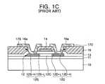
FIG. 1A ,FIG. 1B andFIG. 1C are cross-sectional views showing a TFT with a conventional LDD structure.- Referring to
FIG. 1A , a polycrystalline silicon (poly-Si) layer may be formed by depositing and crystallizing amorphous silicon on aninsulating substrate 10 having abuffer layer 11 using plasma enhanced chemical vapor deposition (PECVD), low pressure chemical vapor deposition (LPCVD), sputtering, or other like methods. - After forming the poly-Si layer, photoresist may then be formed on it to form an active layer, and an
active layer 12 may be formed by patterning the poly-Si layer using the photoresist as a mask. - A
gate insulating layer 13 may then be deposited on theactive layer 12, and a gate metal may be deposited on thegate insulating layer 13. Agate electrode 14 may then be formed by patterning the gate metal. - After forming the
gate electrode 14, low concentration doping may be carried out using thegate electrode 14 as a mask to form an LDD region in the active layer, thus defining source anddrain regions drain regions channel region 12C of the TFT. - Referring to
FIG. 1B , after forming the source anddrain regions photoresist pattern 15, for forming the source anddrain regions insulating substrate 10. - After forming the
photoresist pattern 15,LDD regions 12S-L and12D-L and highly dopedregions 12S-H and12D-H may be formed by performing high concentration doping into the active layer using thephotoresist pattern 15 as a mask. - Referring to
FIG. 1C , after the high concentration doping,contact holes 16a,which expose a portion of the source anddrain regions interlayer insulating layer 16 on an entire surface of theinsulating substrate 10 having thegate electrode 14. - Next, a conductive layer may be deposited on the entire surface of the
insulating substrate 10 and be subjected to photolithography to form source anddrain electrodes drain regions contact holes 16a,thereby forming the TFT. - However, forming the TFT as described above requires a separate mask process to form the LDD region, which increases manufacturing time and cost.
- The present invention provides a TFT having an LDD structure, and an organic electroluminescence display using the same, that may be formed without using a separate mask.
- Additional features of the invention will be set forth in the description which follows, and in part will be apparent from the description, or may be learned by practice of the invention.
- The present invention discloses a TFT comprising a lightly doped drain (LDD) region formation pattern and an active layer formed in an uneven structure on the LDD region formation pattern, and having a source region and a drain region including an LDD region
- The present invention also discloses a display comprising a lightly doped drain (LDD) region formation pattern and a pixel electrode formed on a same layer on an insulating substrate, an active layer formed in an uneven structure on the LDD region formation pattern, and having a source region and a drain region including an LDD region, a gate electrode formed on a gate insulating layer, and a source electrode and a drain electrode coupled to the source and drain regions, respectively. Either the source electrode or the drain electrode is coupled to the pixel electrode.
- The present invention also discloses a TFT comprising a source electrode and a drain electrode formed on an insulating substrate, and an active layer formed in an uneven structure on the source electrode and the drain electrodes and having a source region and a drain region including an LDD region.
- The present invention also discloses a display comprising a source electrode, a drain electrode, and a pixel electrode formed on a same layer on an insulating substrate, and an active layer having a source region and a drain region including an LDD region, and formed in an uneven structure on the source and drain electrodes. A gate insulating layer is formed on an entire surface of the insulating substrate having the active layer, and a gate electrode is formed on the gate insulating layer. An insulating layer is formed on an entire surface of the insulating substrate having the gate electrode, and it has an opening that defines an emission region by exposing a portion of the pixel electrode. An organic layer is formed on the opening of the insulating layer, and an upper electrode is formed on an entire surface of the insulating substrate.
- It is to be understood that both the foregoing general description and the following detailed description are exemplary and explanatory and are intended to provide further explanation of the invention as claimed.
- The accompanying drawings, which are included to provide a further understanding of the invention and are incorporated in and constitute a part of this specification, illustrate embodiments of the invention and together with the description serve to explain the principles of the invention.
FIG. 1A ,FIG. 1B andFIG. 1C are cross-sectional views showing a manufacturing process of a TFT having a conventional LDD structure.FIG. 2A ,FIG. 2B ,FIG. 2C andFIG. 2D are cross-sectional views showing a manufacturing process of an organic electroluminescence display according to a first exemplary embodiment of the present invention.FIG. 3A ,FIG. 3B andFIG. 3C are cross-sectional views showing a manufacturing process of an organic electroluminescence display according to a second exemplary embodiment of the present invention.- Hereinafter, exemplary embodiments of the present invention will be described with reference to the accompanying drawings.
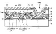
FIG. 2A ,FIG. 2B ,FIG. 2C andFIG. 2D are cross-sectional views showing a manufacturing process of an organic electroluminescence display according to a first exemplary embodiment of the present invention.- Referring to
FIG. 2A , a buffer layer21 (or, diffusion barrier) may be deposited on an insulatingsubstrate 20 by PECVD, LPCVD, sputtering, or other like methods. Thebuffer layer 21 may prevent insulating substrate impurities, such as metal ions, from diffusing and penetrating a poly-Si active layer. - While a glass or plastic substrate may be used as the insulating
substrate 20, glass is preferable. - After forming the
buffer layer 21, apixel electrode 31 and an LDDregion formation pattern 22 may be formed on thebuffer layer 21 by depositing and patterning a transparent conductive material, such as ITO, IZO or other like materials. - Edge portions of the
pixel electrode 31 and the LDDregion formation pattern 22 may have a taper angle of about 10° to about 45°. - Next, an amorphous silicon layer may be deposited on an entire surface of the insulating substrate by PECVD, LPCVD, sputtering, or other like methods. The amorphous silicon layer may be unevenly formed along the shape of the LDD
region formation pattern 22 because the amorphous silicon layer on the edge portion of the LDDregion formation pattern 22 may be formed along the edge portion's taper angle. - A dehydrogenation process may be carried out in a vacuum furnace after forming the amorphous silicon layer. The dehydrogenation process may not be carried out when the amorphous silicon layer is deposited by the LPCVD or sputtering method.
- A poly-Si layer may be formed by crystallizing the amorphous silicon layer through an amorphous silicon crystallization process in which high energy is irradiated to the amorphous silicon layer. A crystallization process using a laser, such as excimer laser annealing (ELA), sequential lateral solidification (SLS) or other like processes, may be employed as the crystallization process.
- After crystallization, a portion of the poly-Si layer on the edge portion of the LDD
region formation pattern 22 may have a lower crystallinity than a portion of the poly-Si layer on the other portion of the LDDregion formation pattern 22. - This is because the portion of the amorphous silicon layer on the edge portion of the LDD
region formation pattern 22 may be thicker than the portion of the amorphous silicon layer on the other portion of the LDDregion formation pattern 22. - After forming the poly-Si layer, photoresist may be formed on the poly-Si layer. Patterning the poly-Si layer using the photoresist as a mask forms an
active layer 23. - The
active layer 23 may be uneven due to the below LDDregion formation pattern 22. A portion of theactive layer 23 on the edge portion of the LDDregion formation pattern 22 may be formed in a shape inclined by 10° to 45° according to the taper angle of the edge portion of the LDDregion formation pattern 22. - Referring to
FIG. 2B , after forming theactive layer 23, agate electrode 25 may be formed by depositing agate insulating layer 24 on theactive layer 23, depositing a gate metal on thegate insulating layer 24, and then patterning the gate metal. - Next, source and
drain regions active layer 23 using thegate electrode 25 as a mask. A region between the source anddrain regions channel region 23C. - An inclined portion of the source and
drain regions region formation pattern 22 may act as a region having a lower doping concentration, namely,LDD regions 23S-L and23D-L, as compared toother portions 23S-H and23D-H of the source anddrain regions region formation pattern 22. Portions of the source anddrain regions region formation pattern 22 may act as highlydoped regions 23S-H and23D-H. - This is because the inclined portion of the
active layer 23 on the edge portion of the LDDregion formation pattern 22 may have less crystallinity than the non-inclined portions of theactive layer 23 formed on other portions of the LDDregion formation pattern 22, resulting in a lower doping degree of impurity. - Referring to
FIG. 2C , after forming the source anddrain regions LDD regions 23S-L and23D-L, aninterlayer insulating layer 26 may be formed on the entire surface of the insulatingsubstrate 10 having thegate electrode 25. - An activation process may then be performed in which doped impurities in the
active layer 23 are further activated through annealing in a furnace. - After performing the annealing process, contact holes26a,which expose a portion of the source and
drain regions interlayer insulating layer 26, while simultaneously forming anopening 26bexposing thepixel electrode 31. - Next, source and
drain electrodes drain regions substrate 20, thus forming the TFT. - Further, either the source electrode or the
drain electrode pixel electrode 31 via theopening 26b.The exemplary embodiment ofFIG. 2C shows thedrain electrode 27D coupled to thepixel electrode 31. - Referring to
FIG. 2D , after forming the source anddrain electrodes passivation layer 28 may be formed on the entire surface of the insulating substrate. Thepassivation layer 28 may be formed by CVD or other like methods, and it may be made of SiO2or SiNx. - Next, an annealing process may be carried out to enhance the TFT's characteristics by curing damage arising during the fabrication process.
- After annealing, a
planarization layer 29 may be formed to remove a step of the lower structure. Theplanarization layer 29 may be formed of acryl, polyimide (PI), polyamide (PA), benzocyclobutene (BCB), or other like materials. - Next, an opening29athat exposes a portion of the
pixel electrode 31 may be formed to define an emission region of the organic light emitting device OLED. - An
organic layer 32 may then be formed on the entire surface of the insulatingsubstrate 20 including thepixel electrode 31. Theorganic layer 32 may comprise several layers according to its function. Generally, in addition to an emission layer, theorganic layer 32 may comprise a multi-layered structure including at least one of a hole injecting layer (HIL), a hole transporting layer (HTL), a hole blocking layer (HBL), an electron transporting layer (ETL), and an electron injecting layer (EIL). - The emission layer emits light having a specific wavelength when electrons and holes, which are injected from a cathode and an anode of the organic electroluminescence device OLED, recombine. At least one of an HIL, HTL, HBL, ETL, EIL, and the like, which have charge transporting capability, may be selectively inserted between an electrode and the emission layer to obtain highly efficient emission.
- When the
pixel electrode 31 of the organic electroluminescence device acts as an anode electrode, a subsequently formed upper electrode may act as a cathode electrode. In this case, an HIL and an HTL may be positioned between thepixel electrode 31 and the emission layer, and an HBL, an ETL and an EIL may be positioned between the emission layer and the subsequently formed upper electrode. - Further, when the
pixel electrode 31 acts as a cathode electrode, the subsequently formed upper electrode may act as an anode electrode, resulting in an organic layer arrangement that may be opposite to the above-described arrangement. - Such an
organic layer 32 including the emission layer may be formed by a wet coating method in which coating is performed in a solution state, such as spin coating, deep coating, spray, screen printing, inkjet printing, or other like methods, or by a dry coating method, such as sputtering, vacuum deposition, or other like methods. - After forming the
organic layer 32, anupper electrode 33 may then be formed on theorganic layer 32, thus forming the organic light emitting device OLED including thepixel electrode 31, theorganic layer 32 and theupper electrode 33. - Although not shown in the drawings, an upper substrate may encapsulate the organic light emitting device OLED.
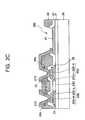
FIG. 3A ,FIG. 3B andFIG. 3C are cross-sectional views showing a manufacturing process of an organic electroluminescence display according to a second exemplary embodiment of the present invention.- Referring to
FIG. 3A , a transparent conductive material, such as ITO, IZO, or other like material, may be deposited and patterned on an insulatingsubstrate 40 having abuffer layer 41 to form source anddrain electrodes pixel electrode 51. - Edge portions of the source and
drain electrodes pixel electrode 51 may have a taper angle of about 10° to about 45°. - Similar to the first embodiment, an
active layer 43 of the TFT may then be formed by depositing an amorphous silicon layer, and forming and patterning a poly-Si layer through a crystallization process using a laser. - After the crystallization process, a portion of the poly-Si layer on the inclined edge portions of the source and
drain electrodes drain electrodes - The
active layer 43 may be unevenly formed due to the below source anddrain electrodes - Referring to
FIG. 3B , after forming theactive layer 43, agate electrode 45 may be formed by depositing agate insulating layer 44 on theactive layer 43, depositing a gate metal on thegate insulating layer 44, and patterning the gate metal. - Next, source and
drain regions active layer 43 using thegate electrode 45 as a mask. A region between the source anddrain regions channel region 43C. - Inclined portions of the source and
drain regions drain electrodes LDD regions 43S-L and43D-L, as compared toportions 43S-H and43D-H of the source anddrain regions drain electrodes portions 43S-H and43D-H of the source anddrain regions drain electrodes doped regions 43S-H and43D-H. - Referring to
FIG. 3C , after forming the source anddrain regions LDD regions 43S-L and43D-L, apassivation layer 46, which may be made of SiO2or SiNx, may be formed on an entire surface of the insulatingsubstrate 40 having thegate electrode 45. - An annealing process may then be carried out in a furnace to further activate the impurities doped into the
active layer 43 and enhance the TFT's characteristics by curing a damaged region arising in the TFT manufacturing process. - A
planarization layer 47 may be formed on the entire surface of the insulatingsubstrate 40 after performing the annealing process. Similar to the first exemplary embodiment, theplanarization layer 47 may be made of acryl, polyimide (PI), polyamide (PA), benzocyclobutene (BCB), or other like materials. - An
opening 47amay then be formed to expose a portion of thepixel electrode 51 and define an emission region of the organic light emitting device OLED. - After forming the opening47a,an
organic layer 52 may be formed on thepixel electrode 51, similarly to the first exemplary embodiment. - Next, an
upper electrode 53 may be formed on theorganic layer 52, thus forming the organic light emitting device OLED including thepixel electrode 51, theorganic layer 52, and theupper electrode 53. - Although not shown, an upper substrate may encapsulate the organic light emitting device OLED.
- For the TFT formed as described above, the LDD region may be formed using one doping process and without a separate additional mask.
- As described above, according to exemplary embodiments of the present invention, a TFT having an LDD structure and an organic electroluminescence display using the same may be achieved without adding a separate mask.
- While the exemplary embodiments described above show an organic electroluminescence display, the present invention is not limited thereto and the TFT of the present invention may be utilized in any device using a TFT.
- It will be apparent to those skilled in the art that various modifications and variation can be made in the present invention without departing from the spirit or scope of the invention. Thus, it is intended that the present invention cover the modifications and variations of this invention provided they come within the scope of the appended claims and their equivalents.
Claims (36)
Priority Applications (1)
| Application Number | Priority Date | Filing Date | Title |
|---|---|---|---|
| US11/832,003US7928444B2 (en) | 2004-04-28 | 2007-08-01 | Thin film transistor and organic electroluminescence display using the same |
Applications Claiming Priority (2)
| Application Number | Priority Date | Filing Date | Title |
|---|---|---|---|
| KR1020040029508AKR100601370B1 (en) | 2004-04-28 | 2004-04-28 | Thin film transistor and organic electroluminescent display using same |
| KR2004-29508 | 2004-04-28 |
Related Child Applications (1)
| Application Number | Title | Priority Date | Filing Date |
|---|---|---|---|
| US11/832,003DivisionUS7928444B2 (en) | 2004-04-28 | 2007-08-01 | Thin film transistor and organic electroluminescence display using the same |
Publications (2)
| Publication Number | Publication Date |
|---|---|
| US20050242348A1true US20050242348A1 (en) | 2005-11-03 |
| US7265384B2 US7265384B2 (en) | 2007-09-04 |
Family
ID=35186175
Family Applications (2)
| Application Number | Title | Priority Date | Filing Date |
|---|---|---|---|
| US11/095,601Expired - LifetimeUS7265384B2 (en) | 2004-04-28 | 2005-04-01 | Thin film transistor and organic electroluminescence display using the same |
| US11/832,003Expired - LifetimeUS7928444B2 (en) | 2004-04-28 | 2007-08-01 | Thin film transistor and organic electroluminescence display using the same |
Family Applications After (1)
| Application Number | Title | Priority Date | Filing Date |
|---|---|---|---|
| US11/832,003Expired - LifetimeUS7928444B2 (en) | 2004-04-28 | 2007-08-01 | Thin film transistor and organic electroluminescence display using the same |
Country Status (3)
| Country | Link |
|---|---|
| US (2) | US7265384B2 (en) |
| KR (1) | KR100601370B1 (en) |
| CN (1) | CN100544029C (en) |
Cited By (4)
| Publication number | Priority date | Publication date | Assignee | Title |
|---|---|---|---|---|
| US20060238115A1 (en)* | 2005-04-21 | 2006-10-26 | Lee Ho-Nyeon | Active matrix organic light emitting device and method of manufacturing the same |
| US20070075633A1 (en)* | 2005-09-30 | 2007-04-05 | Seiko Epson Corporation | Organic electroluminescence device and electronic apparatus |
| US20140346448A1 (en)* | 2013-05-21 | 2014-11-27 | Samsung Display Co., Ltd. | Organic light-emitting display apparatus and method of manufacturing the same |
| US20160306472A1 (en)* | 2015-04-16 | 2016-10-20 | Samsung Display Co., Ltd. | Display device |
Families Citing this family (23)
| Publication number | Priority date | Publication date | Assignee | Title |
|---|---|---|---|---|
| KR100839470B1 (en)* | 2007-01-12 | 2008-06-19 | 엘지전자 주식회사 | Organic electroluminescent display and manufacturing method thereof |
| JP5515281B2 (en)* | 2008-12-03 | 2014-06-11 | ソニー株式会社 | THIN FILM TRANSISTOR, DISPLAY DEVICE, ELECTRONIC DEVICE, AND METHOD FOR PRODUCING THIN FILM TRANSISTOR |
| JP4752927B2 (en)* | 2009-02-09 | 2011-08-17 | ソニー株式会社 | Thin film transistor and display device |
| KR101065413B1 (en) | 2009-07-03 | 2011-09-16 | 삼성모바일디스플레이주식회사 | Organic light emitting display device and manufacturing method |
| KR101041144B1 (en)* | 2009-08-13 | 2011-06-13 | 삼성모바일디스플레이주식회사 | Thin film transistor, manufacturing method thereof and organic light emitting display device comprising same |
| KR20110024531A (en)* | 2009-09-02 | 2011-03-09 | 삼성모바일디스플레이주식회사 | Organic light emitting display device |
| KR101084256B1 (en) | 2009-12-08 | 2011-11-16 | 삼성모바일디스플레이주식회사 | Organic light emitting display device and manufacturing method thereof |
| KR20250048807A (en) | 2009-12-25 | 2025-04-10 | 가부시키가이샤 한도오따이 에네루기 켄큐쇼 | Semiconductor device |
| KR101839930B1 (en)* | 2010-12-29 | 2018-04-27 | 삼성디스플레이 주식회사 | Organic light emitting display apparatus and method of manufacturing organic light emitting display apparatus |
| KR102070951B1 (en)* | 2013-05-23 | 2020-01-30 | 삼성디스플레이 주식회사 | Organic light emitting display device and method of fabricating the same |
| KR20150137214A (en)* | 2014-05-28 | 2015-12-09 | 삼성디스플레이 주식회사 | Organic light-emitting display apparatus and manufacturing the same |
| CN104992926B (en)* | 2015-07-24 | 2018-03-13 | 深圳市华星光电技术有限公司 | LTPS array base paltes and its manufacture method |
| KR102391346B1 (en)* | 2015-08-04 | 2022-04-28 | 삼성디스플레이 주식회사 | Organic light display apparatus, apparatus for organic layer deposition, and method for manufacturing of organic light emitting display apparatus using the same |
| CN105140128B (en)* | 2015-09-08 | 2018-01-02 | 信利(惠州)智能显示有限公司 | Low-temperature polysilicon film transistor and preparation method thereof |
| US10361385B2 (en) | 2016-02-12 | 2019-07-23 | Samsung Display Co., Ltd. | Display device |
| KR102505879B1 (en)* | 2016-03-24 | 2023-03-06 | 삼성디스플레이 주식회사 | Display apparatus |
| CN106057735B (en)* | 2016-06-07 | 2019-04-02 | 深圳市华星光电技术有限公司 | The production method and TFT backplate of TFT backplate |
| CN107221497B (en)* | 2017-07-28 | 2020-07-21 | 京东方科技集团股份有限公司 | Manufacturing method of lead and display panel |
| CN109244081B (en)* | 2018-08-30 | 2021-06-22 | 武汉华星光电半导体显示技术有限公司 | Array substrate and display panel |
| CN109300990B (en)* | 2018-09-29 | 2022-04-22 | 合肥鑫晟光电科技有限公司 | Thin film transistor and preparation method, array substrate, display panel and display device |
| CN110021653B (en)* | 2019-04-23 | 2021-02-12 | 合肥鑫晟光电科技有限公司 | Array substrate, manufacturing method thereof, display panel and display device |
| CN111834395A (en)* | 2019-09-30 | 2020-10-27 | 昆山国显光电有限公司 | Transparent display panel, display device and display panel thereof |
| CN115000087B (en)* | 2022-05-26 | 2025-09-26 | 武汉华星光电技术有限公司 | Array substrate and preparation method thereof |
Citations (6)
| Publication number | Priority date | Publication date | Assignee | Title |
|---|---|---|---|---|
| US5585647A (en)* | 1993-06-29 | 1996-12-17 | Kabushiki Kaisha Toshiba | Integrated circuit device having an insulating substrate, and a liquid crystal display device having an insulating substrate |
| US5821565A (en)* | 1988-06-29 | 1998-10-13 | Hitachi, Ltd. | Thin film transistor structure having increased on-current |
| US6563136B2 (en)* | 2000-08-10 | 2003-05-13 | Sony Corporation | Thin-film semiconductor device having a thin-film transistor for circuits that differs from a thin-film transistor for pixels |
| US20040206956A1 (en)* | 2001-08-02 | 2004-10-21 | Fujitsu Dispaly Technologies Corporation | Thin film transistor device and method of manufacturing the same |
| US6835586B2 (en)* | 1998-12-25 | 2004-12-28 | Semiconductor Energy Laboratory Co., Ltd. | Semiconductor device and manufacturing method thereof |
| US6909114B1 (en)* | 1998-11-17 | 2005-06-21 | Semiconductor Energy Laboratory Co., Ltd. | Semiconductor device having LDD regions |
Family Cites Families (7)
| Publication number | Priority date | Publication date | Assignee | Title |
|---|---|---|---|---|
| JP2794678B2 (en)* | 1991-08-26 | 1998-09-10 | 株式会社 半導体エネルギー研究所 | Insulated gate semiconductor device and method of manufacturing the same |
| JP4202502B2 (en)* | 1998-12-28 | 2008-12-24 | 株式会社半導体エネルギー研究所 | Semiconductor device |
| JP3645755B2 (en)* | 1999-09-17 | 2005-05-11 | 日本電気株式会社 | Thin film transistor and manufacturing method thereof |
| KR100582198B1 (en)* | 2000-02-24 | 2006-05-24 | 엘지.필립스 엘시디 주식회사 | Manufacturing method of complementary MOS thin film transistor |
| JP4836339B2 (en) | 2000-03-06 | 2011-12-14 | 株式会社半導体エネルギー研究所 | Semiconductor display device and manufacturing method thereof |
| JP4982918B2 (en) | 2000-10-13 | 2012-07-25 | 日本電気株式会社 | Liquid crystal display substrate and manufacturing method thereof |
| KR100491141B1 (en)* | 2001-03-02 | 2005-05-24 | 삼성에스디아이 주식회사 | TFT and Method for Fabricating the Same and Active Matrix display device and Method for fabricating the Same using the TFT |
- 2004
- 2004-04-28KRKR1020040029508Apatent/KR100601370B1/ennot_activeExpired - Lifetime
- 2005
- 2005-04-01USUS11/095,601patent/US7265384B2/ennot_activeExpired - Lifetime
- 2005-04-15CNCNB2005100659518Apatent/CN100544029C/ennot_activeExpired - Lifetime
- 2007
- 2007-08-01USUS11/832,003patent/US7928444B2/ennot_activeExpired - Lifetime
Patent Citations (6)
| Publication number | Priority date | Publication date | Assignee | Title |
|---|---|---|---|---|
| US5821565A (en)* | 1988-06-29 | 1998-10-13 | Hitachi, Ltd. | Thin film transistor structure having increased on-current |
| US5585647A (en)* | 1993-06-29 | 1996-12-17 | Kabushiki Kaisha Toshiba | Integrated circuit device having an insulating substrate, and a liquid crystal display device having an insulating substrate |
| US6909114B1 (en)* | 1998-11-17 | 2005-06-21 | Semiconductor Energy Laboratory Co., Ltd. | Semiconductor device having LDD regions |
| US6835586B2 (en)* | 1998-12-25 | 2004-12-28 | Semiconductor Energy Laboratory Co., Ltd. | Semiconductor device and manufacturing method thereof |
| US6563136B2 (en)* | 2000-08-10 | 2003-05-13 | Sony Corporation | Thin-film semiconductor device having a thin-film transistor for circuits that differs from a thin-film transistor for pixels |
| US20040206956A1 (en)* | 2001-08-02 | 2004-10-21 | Fujitsu Dispaly Technologies Corporation | Thin film transistor device and method of manufacturing the same |
Cited By (10)
| Publication number | Priority date | Publication date | Assignee | Title |
|---|---|---|---|---|
| US10649569B2 (en)* | 2005-04-16 | 2020-05-12 | Samsung Display Co., Ltd. | Display device |
| US20060238115A1 (en)* | 2005-04-21 | 2006-10-26 | Lee Ho-Nyeon | Active matrix organic light emitting device and method of manufacturing the same |
| US7626331B2 (en)* | 2005-04-21 | 2009-12-01 | Samsung Electronics Co., Ltd. | Active matrix organic light emitting device having organic thin film transistor disposed on organic light emitting diode structure |
| US20070075633A1 (en)* | 2005-09-30 | 2007-04-05 | Seiko Epson Corporation | Organic electroluminescence device and electronic apparatus |
| US20140346448A1 (en)* | 2013-05-21 | 2014-11-27 | Samsung Display Co., Ltd. | Organic light-emitting display apparatus and method of manufacturing the same |
| US9040993B2 (en)* | 2013-05-21 | 2015-05-26 | Samsung Display Co., Ltd. | Organic light-emitting display apparatus and method of manufacturing the same |
| US20160306472A1 (en)* | 2015-04-16 | 2016-10-20 | Samsung Display Co., Ltd. | Display device |
| US10198103B2 (en)* | 2015-04-16 | 2019-02-05 | Samsung Display Co., Ltd. | Display device |
| US11137848B2 (en) | 2015-04-16 | 2021-10-05 | Samsung Display Co., Ltd. | Display device |
| US11599215B2 (en) | 2015-04-16 | 2023-03-07 | Samsung Display Co., Ltd. | Display device |
Also Published As
| Publication number | Publication date |
|---|---|
| KR100601370B1 (en) | 2006-07-13 |
| KR20050104157A (en) | 2005-11-02 |
| US7265384B2 (en) | 2007-09-04 |
| US7928444B2 (en) | 2011-04-19 |
| CN100544029C (en) | 2009-09-23 |
| US20080035932A1 (en) | 2008-02-14 |
| CN1691356A (en) | 2005-11-02 |
Similar Documents
| Publication | Publication Date | Title |
|---|---|---|
| US7928444B2 (en) | Thin film transistor and organic electroluminescence display using the same | |
| US8278664B2 (en) | Organic light emitting display device and method of fabricating the same | |
| US8283860B2 (en) | Organic light emitting display device and method of fabricating the same | |
| US7728510B2 (en) | Organic light emitting display with auxiliary electrode line and method of fabricating the same | |
| US7598111B2 (en) | Thin film transistor and method of manufacturing the same | |
| CN102082164B (en) | Oled display apparatus and method of manufacturing the same | |
| US7915102B2 (en) | Methods of fabricating thin film transistor and organic light emitting display device using the same | |
| US20120326174A1 (en) | Organic light-emitting display device and method of manufacturing the same | |
| JP5084184B2 (en) | Organic thin film transistor, manufacturing method thereof, and organic light emitting display device including the same | |
| KR100611155B1 (en) | Organic electroluminescent display and manufacturing method thereof | |
| US7189995B2 (en) | Organic electroluminescence display device and method for fabricating the same | |
| KR100685803B1 (en) | Method for manufacturing organic electroluminescent device | |
| KR100805155B1 (en) | Organic EL display device having thin film transistor and manufacturing method thereof | |
| KR100669457B1 (en) | Thin film transistor, flat panel display device with the thin film transistor and method of manufacturing the same | |
| US7629738B2 (en) | Organic electroluminescence display device providing uniformity of color coordinates by controlling inorganic layer thickness deviation | |
| KR100592267B1 (en) | Manufacturing method of organic electroluminescent display | |
| KR100943953B1 (en) | Manufacturing method of display device | |
| KR101225347B1 (en) | Fabrication method of poly-silicon layer and fabrication method of Thin Film Transistor and organic electroluminescence display device using it | |
| KR101854703B1 (en) | Organic light emitting display device | |
| KR20050077832A (en) | Tft and flat panel display therewith | |
| KR100669415B1 (en) | Thin Film Transistor Manufacturing Method | |
| KR100635059B1 (en) | Organic electroluminescent display |
Legal Events
| Date | Code | Title | Description |
|---|---|---|---|
| AS | Assignment | Owner name:SAMSUNG SDI CO., LTD., KOREA, REPUBLIC OF Free format text:ASSIGNMENT OF ASSIGNORS INTEREST;ASSIGNOR:OH, SANG-HUN;REEL/FRAME:016445/0630 Effective date:20050317 | |
| STCF | Information on status: patent grant | Free format text:PATENTED CASE | |
| FEPP | Fee payment procedure | Free format text:PAYOR NUMBER ASSIGNED (ORIGINAL EVENT CODE: ASPN); ENTITY STATUS OF PATENT OWNER: LARGE ENTITY | |
| AS | Assignment | Owner name:SAMSUNG MOBILE DISPLAY CO., LTD., KOREA, REPUBLIC Free format text:ASSIGNMENT OF ASSIGNORS INTEREST;ASSIGNOR:SAMSUNG SDI CO., LTD.;REEL/FRAME:022024/0026 Effective date:20081212 Owner name:SAMSUNG MOBILE DISPLAY CO., LTD.,KOREA, REPUBLIC O Free format text:ASSIGNMENT OF ASSIGNORS INTEREST;ASSIGNOR:SAMSUNG SDI CO., LTD.;REEL/FRAME:022024/0026 Effective date:20081212 | |
| FPAY | Fee payment | Year of fee payment:4 | |
| AS | Assignment | Owner name:SAMSUNG DISPLAY CO., LTD., KOREA, REPUBLIC OF Free format text:MERGER;ASSIGNOR:SAMSUNG MOBILE DISPLAY CO., LTD.;REEL/FRAME:028868/0387 Effective date:20120702 | |
| FEPP | Fee payment procedure | Free format text:PAYOR NUMBER ASSIGNED (ORIGINAL EVENT CODE: ASPN); ENTITY STATUS OF PATENT OWNER: LARGE ENTITY Free format text:PAYER NUMBER DE-ASSIGNED (ORIGINAL EVENT CODE: RMPN); ENTITY STATUS OF PATENT OWNER: LARGE ENTITY | |
| FPAY | Fee payment | Year of fee payment:8 | |
| MAFP | Maintenance fee payment | Free format text:PAYMENT OF MAINTENANCE FEE, 12TH YEAR, LARGE ENTITY (ORIGINAL EVENT CODE: M1553); ENTITY STATUS OF PATENT OWNER: LARGE ENTITY Year of fee payment:12 |