US20050230356A1 - Methods of making, positioning and orienting nanostructures, nanostructure arrays and nanostructure devices - Google Patents
Methods of making, positioning and orienting nanostructures, nanostructure arrays and nanostructure devicesDownload PDFInfo
- Publication number
- US20050230356A1 US20050230356A1US11/142,563US14256305AUS2005230356A1US 20050230356 A1US20050230356 A1US 20050230356A1US 14256305 AUS14256305 AUS 14256305AUS 2005230356 A1US2005230356 A1US 2005230356A1
- Authority
- US
- United States
- Prior art keywords
- nanostructure
- nanostructures
- etchable
- substrate
- catalyst
- Prior art date
- Legal status (The legal status is an assumption and is not a legal conclusion. Google has not performed a legal analysis and makes no representation as to the accuracy of the status listed.)
- Granted
Links
- 239000002086nanomaterialSubstances0.000titleclaimsabstractdescription905
- 238000000034methodMethods0.000titleclaimsabstractdescription236
- 238000003491arrayMethods0.000titleabstractdescription84
- 239000002070nanowireSubstances0.000claimsdescription209
- 239000000463materialSubstances0.000claimsdescription179
- 239000000758substrateSubstances0.000claimsdescription179
- 238000005530etchingMethods0.000claimsdescription23
- 239000002071nanotubeSubstances0.000claimsdescription22
- 239000002073nanorodSubstances0.000claimsdescription21
- VYPSYNLAJGMNEJ-UHFFFAOYSA-NSilicium dioxideChemical compoundO=[Si]=OVYPSYNLAJGMNEJ-UHFFFAOYSA-N0.000claimsdescription19
- 229910052814silicon oxideInorganic materials0.000claimsdescription13
- 239000002074nanoribbonSubstances0.000claimsdescription8
- 238000003306harvestingMethods0.000claimsdescription7
- 238000004519manufacturing processMethods0.000abstractdescription27
- 239000003054catalystSubstances0.000description229
- 239000002243precursorSubstances0.000description121
- 239000007789gasSubstances0.000description99
- 239000002019doping agentSubstances0.000description89
- 230000015572biosynthetic processEffects0.000description82
- 238000003556assayMethods0.000description70
- 210000002381plasmaAnatomy0.000description69
- 238000003786synthesis reactionMethods0.000description55
- 239000002245particleSubstances0.000description51
- 239000012530fluidSubstances0.000description48
- 239000004065semiconductorSubstances0.000description45
- 239000000203mixtureSubstances0.000description38
- XEEYBQQBJWHFJM-UHFFFAOYSA-NIronChemical compound[Fe]XEEYBQQBJWHFJM-UHFFFAOYSA-N0.000description35
- 239000000047productSubstances0.000description35
- PCHJSUWPFVWCPO-UHFFFAOYSA-NgoldChemical compound[Au]PCHJSUWPFVWCPO-UHFFFAOYSA-N0.000description33
- 229910052710siliconInorganic materials0.000description33
- 230000008569processEffects0.000description32
- 230000005684electric fieldEffects0.000description31
- XUIMIQQOPSSXEZ-UHFFFAOYSA-NSiliconChemical compound[Si]XUIMIQQOPSSXEZ-UHFFFAOYSA-N0.000description29
- 239000010931goldSubstances0.000description29
- 229910052737goldInorganic materials0.000description28
- 239000010703siliconSubstances0.000description28
- 239000000725suspensionSubstances0.000description28
- 239000000084colloidal systemSubstances0.000description24
- 239000013078crystalSubstances0.000description23
- 238000000605extractionMethods0.000description22
- 239000000126substanceSubstances0.000description22
- 238000000151depositionMethods0.000description21
- 238000013459approachMethods0.000description18
- 238000001514detection methodMethods0.000description18
- 229910052742ironInorganic materials0.000description18
- 239000012491analyteSubstances0.000description15
- 230000008859changeEffects0.000description15
- -1nanodotsSubstances0.000description15
- 239000002096quantum dotSubstances0.000description15
- 239000010410layerSubstances0.000description13
- 229910052751metalInorganic materials0.000description13
- 239000002184metalSubstances0.000description13
- 230000002441reversible effectEffects0.000description13
- 239000002159nanocrystalSubstances0.000description12
- 239000000523sampleSubstances0.000description12
- 238000000059patterningMethods0.000description11
- JBRZTFJDHDCESZ-UHFFFAOYSA-NAsGaChemical compound[As]#[Ga]JBRZTFJDHDCESZ-UHFFFAOYSA-N0.000description10
- 229910001218Gallium arsenideInorganic materials0.000description10
- 230000001276controlling effectEffects0.000description10
- 238000009826distributionMethods0.000description10
- 238000010438heat treatmentMethods0.000description10
- 229910052738indiumInorganic materials0.000description10
- 238000012545processingMethods0.000description10
- 239000002585baseSubstances0.000description9
- 229910052796boronInorganic materials0.000description9
- 238000006243chemical reactionMethods0.000description9
- 238000010276constructionMethods0.000description9
- 238000005516engineering processMethods0.000description9
- 230000033001locomotionEffects0.000description9
- 229910052698phosphorusInorganic materials0.000description9
- 229920000642polymerPolymers0.000description9
- 230000004044responseEffects0.000description9
- IJGRMHOSHXDMSA-UHFFFAOYSA-NAtomic nitrogenChemical compoundN#NIJGRMHOSHXDMSA-UHFFFAOYSA-N0.000description8
- 229910052785arsenicInorganic materials0.000description8
- 238000003776cleavage reactionMethods0.000description8
- 230000008021depositionEffects0.000description8
- 229910052732germaniumInorganic materials0.000description8
- 230000000737periodic effectEffects0.000description8
- 230000007017scissionEffects0.000description8
- 102000004190EnzymesHuman genes0.000description7
- 108090000790EnzymesProteins0.000description7
- 230000008901benefitEffects0.000description7
- 229910017052cobaltInorganic materials0.000description7
- 239000010941cobaltSubstances0.000description7
- GUTLYIVDDKVIGB-UHFFFAOYSA-Ncobalt atomChemical compound[Co]GUTLYIVDDKVIGB-UHFFFAOYSA-N0.000description7
- 229940088598enzymeDrugs0.000description7
- 230000005669field effectEffects0.000description7
- 239000007788liquidSubstances0.000description7
- 102000004169proteins and genesHuman genes0.000description7
- 108090000623proteins and genesProteins0.000description7
- QGZKDVFQNNGYKY-UHFFFAOYSA-NAmmoniaChemical compoundNQGZKDVFQNNGYKY-UHFFFAOYSA-N0.000description6
- BLRPTPMANUNPDV-UHFFFAOYSA-NSilaneChemical compound[SiH4]BLRPTPMANUNPDV-UHFFFAOYSA-N0.000description6
- UHYPYGJEEGLRJD-UHFFFAOYSA-Ncadmium(2+);selenium(2-)Chemical compound[Se-2].[Cd+2]UHYPYGJEEGLRJD-UHFFFAOYSA-N0.000description6
- 125000000524functional groupChemical group0.000description6
- 229910052733galliumInorganic materials0.000description6
- 239000011521glassSubstances0.000description6
- 238000000608laser ablationMethods0.000description6
- 239000003446ligandSubstances0.000description6
- 230000003287optical effectEffects0.000description6
- 239000007787solidSubstances0.000description6
- 235000012431wafersNutrition0.000description6
- OKTJSMMVPCPJKN-UHFFFAOYSA-NCarbonChemical compound[C]OKTJSMMVPCPJKN-UHFFFAOYSA-N0.000description5
- PNEYBMLMFCGWSK-UHFFFAOYSA-Naluminium oxideInorganic materials[O-2].[O-2].[O-2].[Al+3].[Al+3]PNEYBMLMFCGWSK-UHFFFAOYSA-N0.000description5
- 150000001412aminesChemical class0.000description5
- 239000002041carbon nanotubeSubstances0.000description5
- 150000001875compoundsChemical class0.000description5
- 230000000694effectsEffects0.000description5
- 238000001962electrophoresisMethods0.000description5
- 239000002105nanoparticleSubstances0.000description5
- 239000004054semiconductor nanocrystalSubstances0.000description5
- 235000012239silicon dioxideNutrition0.000description5
- 230000003068static effectEffects0.000description5
- WQZGKKKJIJFFOK-GASJEMHNSA-NGlucoseNatural productsOC[C@H]1OC(O)[C@H](O)[C@@H](O)[C@@H]1OWQZGKKKJIJFFOK-GASJEMHNSA-N0.000description4
- 229910000673Indium arsenideInorganic materials0.000description4
- 239000000443aerosolSubstances0.000description4
- 229910045601alloyInorganic materials0.000description4
- 239000000956alloySubstances0.000description4
- 229910021393carbon nanotubeInorganic materials0.000description4
- HVYWMOMLDIMFJA-DPAQBDIFSA-NcholesterolChemical compoundC1C=C2C[C@@H](O)CC[C@]2(C)[C@@H]2[C@@H]1[C@@H]1CC[C@H]([C@H](C)CCCC(C)C)[C@@]1(C)CC2HVYWMOMLDIMFJA-DPAQBDIFSA-N0.000description4
- 238000000576coating methodMethods0.000description4
- 239000000470constituentSubstances0.000description4
- 230000008878couplingEffects0.000description4
- 238000010168coupling processMethods0.000description4
- 238000005859coupling reactionMethods0.000description4
- 239000002178crystalline materialSubstances0.000description4
- 239000012717electrostatic precipitatorSubstances0.000description4
- 230000005496eutecticsEffects0.000description4
- 239000012634fragmentSubstances0.000description4
- 230000006870functionEffects0.000description4
- 239000008103glucoseSubstances0.000description4
- RPQDHPTXJYYUPQ-UHFFFAOYSA-Nindium arsenideChemical compound[In]#[As]RPQDHPTXJYYUPQ-UHFFFAOYSA-N0.000description4
- 230000000873masking effectEffects0.000description4
- 229910044991metal oxideInorganic materials0.000description4
- 150000004706metal oxidesChemical class0.000description4
- 150000004767nitridesChemical class0.000description4
- 229910052757nitrogenInorganic materials0.000description4
- 229910052756noble gasInorganic materials0.000description4
- 125000002924primary amino groupChemical class[H]N([H])*0.000description4
- 239000010453quartzSubstances0.000description4
- 229910052711seleniumInorganic materials0.000description4
- 239000002094self assembled monolayerSubstances0.000description4
- 229910052714telluriumInorganic materials0.000description4
- 229910017115AlSbInorganic materials0.000description3
- UHOVQNZJYSORNB-UHFFFAOYSA-NBenzeneChemical compoundC1=CC=CC=C1UHOVQNZJYSORNB-UHFFFAOYSA-N0.000description3
- LFQSCWFLJHTTHZ-UHFFFAOYSA-NEthanolChemical compoundCCOLFQSCWFLJHTTHZ-UHFFFAOYSA-N0.000description3
- 229910005542GaSbInorganic materials0.000description3
- 108010015776Glucose oxidaseProteins0.000description3
- PWHULOQIROXLJO-UHFFFAOYSA-NManganeseChemical compound[Mn]PWHULOQIROXLJO-UHFFFAOYSA-N0.000description3
- 229910017920NH3OHInorganic materials0.000description3
- 229910000577Silicon-germaniumInorganic materials0.000description3
- YXFVVABEGXRONW-UHFFFAOYSA-NTolueneChemical compoundCC1=CC=CC=C1YXFVVABEGXRONW-UHFFFAOYSA-N0.000description3
- 229910052782aluminiumInorganic materials0.000description3
- 229910021529ammoniaInorganic materials0.000description3
- 239000000427antigenSubstances0.000description3
- 102000036639antigensHuman genes0.000description3
- 108091007433antigensProteins0.000description3
- 230000003197catalytic effectEffects0.000description3
- 238000004140cleaningMethods0.000description3
- 239000011248coating agentSubstances0.000description3
- 238000009833condensationMethods0.000description3
- 230000005494condensationEffects0.000description3
- 239000011258core-shell materialSubstances0.000description3
- 238000013500data storageMethods0.000description3
- 230000004907fluxEffects0.000description3
- 235000019420glucose oxidaseNutrition0.000description3
- 229910052739hydrogenInorganic materials0.000description3
- 239000001257hydrogenSubstances0.000description3
- 238000010348incorporationMethods0.000description3
- WPYVAWXEWQSOGY-UHFFFAOYSA-Nindium antimonideChemical compound[Sb]#[In]WPYVAWXEWQSOGY-UHFFFAOYSA-N0.000description3
- 230000010354integrationEffects0.000description3
- 230000003993interactionEffects0.000description3
- 230000002427irreversible effectEffects0.000description3
- 229910052748manganeseInorganic materials0.000description3
- 239000011572manganeseSubstances0.000description3
- 238000005259measurementMethods0.000description3
- 230000007246mechanismEffects0.000description3
- 238000002844meltingMethods0.000description3
- 230000008018meltingEffects0.000description3
- 150000002739metalsChemical class0.000description3
- 150000007523nucleic acidsChemical class0.000description3
- 102000039446nucleic acidsHuman genes0.000description3
- 108020004707nucleic acidsProteins0.000description3
- 230000003647oxidationEffects0.000description3
- 238000007254oxidation reactionMethods0.000description3
- 238000000206photolithographyMethods0.000description3
- 238000002360preparation methodMethods0.000description3
- 238000003672processing methodMethods0.000description3
- 239000013545self-assembled monolayerSubstances0.000description3
- 229910052717sulfurInorganic materials0.000description3
- 238000007740vapor depositionMethods0.000description3
- YBJHBAHKTGYVGT-ZKWXMUAHSA-N(+)-BiotinChemical compoundN1C(=O)N[C@@H]2[C@H](CCCCC(=O)O)SC[C@@H]21YBJHBAHKTGYVGT-ZKWXMUAHSA-N0.000description2
- YBNMDCCMCLUHBL-UHFFFAOYSA-N(2,5-dioxopyrrolidin-1-yl) 4-pyren-1-ylbutanoateChemical compoundC=1C=C(C2=C34)C=CC3=CC=CC4=CC=C2C=1CCCC(=O)ON1C(=O)CCC1=OYBNMDCCMCLUHBL-UHFFFAOYSA-N0.000description2
- XMWRBQBLMFGWIX-UHFFFAOYSA-NC60 fullereneChemical compoundC12=C3C(C4=C56)=C7C8=C5C5=C9C%10=C6C6=C4C1=C1C4=C6C6=C%10C%10=C9C9=C%11C5=C8C5=C8C7=C3C3=C7C2=C1C1=C2C4=C6C4=C%10C6=C9C9=C%11C5=C5C8=C3C3=C7C1=C1C2=C4C6=C2C9=C5C3=C12XMWRBQBLMFGWIX-UHFFFAOYSA-N0.000description2
- 229910004613CdTeInorganic materials0.000description2
- ULGZDMOVFRHVEP-RWJQBGPGSA-NErythromycinChemical compoundO([C@@H]1[C@@H](C)C(=O)O[C@@H]([C@@]([C@H](O)[C@@H](C)C(=O)[C@H](C)C[C@@](C)(O)[C@H](O[C@H]2[C@@H]([C@H](C[C@@H](C)O2)N(C)C)O)[C@H]1C)(C)O)CC)[C@H]1C[C@@](C)(OC)[C@@H](O)[C@H](C)O1ULGZDMOVFRHVEP-RWJQBGPGSA-N0.000description2
- 239000004366Glucose oxidaseSubstances0.000description2
- 229910004262HgTeInorganic materials0.000description2
- UFHFLCQGNIYNRP-UHFFFAOYSA-NHydrogenChemical compound[H][H]UFHFLCQGNIYNRP-UHFFFAOYSA-N0.000description2
- 108090000854OxidoreductasesProteins0.000description2
- 102000004316OxidoreductasesHuman genes0.000description2
- 229910002665PbTeInorganic materials0.000description2
- 229910052581Si3N4Inorganic materials0.000description2
- MUMGGOZAMZWBJJ-DYKIIFRCSA-NTestostosteroneChemical compoundO=C1CC[C@]2(C)[C@H]3CC[C@](C)([C@H](CC4)O)[C@@H]4[C@@H]3CCC2=C1MUMGGOZAMZWBJJ-DYKIIFRCSA-N0.000description2
- 229910007709ZnTeInorganic materials0.000description2
- 239000002253acidSubstances0.000description2
- 150000007513acidsChemical class0.000description2
- 230000009471actionEffects0.000description2
- 230000002776aggregationEffects0.000description2
- 238000004220aggregationMethods0.000description2
- 238000000429assemblyMethods0.000description2
- 230000000712assemblyEffects0.000description2
- JRPBQTZRNDNNOP-UHFFFAOYSA-Nbarium titanateChemical compound[Ba+2].[Ba+2].[O-][Ti]([O-])([O-])[O-]JRPBQTZRNDNNOP-UHFFFAOYSA-N0.000description2
- 229910002113barium titanateInorganic materials0.000description2
- WQZGKKKJIJFFOK-VFUOTHLCSA-Nbeta-D-glucoseChemical compoundOC[C@H]1O[C@@H](O)[C@H](O)[C@@H](O)[C@@H]1OWQZGKKKJIJFFOK-VFUOTHLCSA-N0.000description2
- 230000002902bimodal effectEffects0.000description2
- 238000004166bioassayMethods0.000description2
- 238000004364calculation methodMethods0.000description2
- 210000004027cellAnatomy0.000description2
- 239000003795chemical substances by applicationSubstances0.000description2
- 238000001816coolingMethods0.000description2
- 229910021419crystalline siliconInorganic materials0.000description2
- 230000007423decreaseEffects0.000description2
- 230000003247decreasing effectEffects0.000description2
- 230000001419dependent effectEffects0.000description2
- 238000013461designMethods0.000description2
- 238000009792diffusion processMethods0.000description2
- 230000005672electromagnetic fieldEffects0.000description2
- 238000002875fluorescence polarizationMethods0.000description2
- 238000002866fluorescence resonance energy transferMethods0.000description2
- 229910003472fullereneInorganic materials0.000description2
- 238000003205genotyping methodMethods0.000description2
- GNPVGFCGXDBREM-UHFFFAOYSA-Ngermanium atomChemical compound[Ge]GNPVGFCGXDBREM-UHFFFAOYSA-N0.000description2
- 229940116332glucose oxidaseDrugs0.000description2
- 239000013056hazardous productSubstances0.000description2
- 230000000977initiatory effectEffects0.000description2
- 239000012212insulatorSubstances0.000description2
- 238000010329laser etchingMethods0.000description2
- 230000000670limiting effectEffects0.000description2
- WPBNNNQJVZRUHP-UHFFFAOYSA-Lmanganese(2+);methyl n-[[2-(methoxycarbonylcarbamothioylamino)phenyl]carbamothioyl]carbamate;n-[2-(sulfidocarbothioylamino)ethyl]carbamodithioateChemical compound[Mn+2].[S-]C(=S)NCCNC([S-])=S.COC(=O)NC(=S)NC1=CC=CC=C1NC(=S)NC(=O)OCWPBNNNQJVZRUHP-UHFFFAOYSA-L0.000description2
- 230000001404mediated effectEffects0.000description2
- 108020004999messenger RNAProteins0.000description2
- VNWKTOKETHGBQD-UHFFFAOYSA-NmethaneChemical groupCVNWKTOKETHGBQD-UHFFFAOYSA-N0.000description2
- 238000000386microscopyMethods0.000description2
- 238000007639printingMethods0.000description2
- 238000010791quenchingMethods0.000description2
- 230000000171quenching effectEffects0.000description2
- 230000001105regulatory effectEffects0.000description2
- SBIBMFFZSBJNJF-UHFFFAOYSA-Nselenium;zincChemical compound[Se]=[Zn]SBIBMFFZSBJNJF-UHFFFAOYSA-N0.000description2
- 229910000077silaneInorganic materials0.000description2
- 229910010271silicon carbideInorganic materials0.000description2
- 229910052709silverInorganic materials0.000description2
- 239000002109single walled nanotubeSubstances0.000description2
- 238000010561standard procedureMethods0.000description2
- 238000002198surface plasmon resonance spectroscopyMethods0.000description2
- 238000001308synthesis methodMethods0.000description2
- OCGWQDWYSQAFTO-UHFFFAOYSA-NtellanylideneleadChemical compound[Pb]=[Te]OCGWQDWYSQAFTO-UHFFFAOYSA-N0.000description2
- 238000012360testing methodMethods0.000description2
- 238000002207thermal evaporationMethods0.000description2
- 229910052718tinInorganic materials0.000description2
- 230000008016vaporizationEffects0.000description2
- PJVWKTKQMONHTI-UHFFFAOYSA-NwarfarinChemical compoundOC=1C2=CC=CC=C2OC(=O)C=1C(CC(=O)C)C1=CC=CC=C1PJVWKTKQMONHTI-UHFFFAOYSA-N0.000description2
- 229960005080warfarinDrugs0.000description2
- 238000009736wettingMethods0.000description2
- 229910018873(CdSe)ZnSInorganic materials0.000description1
- 108010031132Alcohol OxidoreductasesProteins0.000description1
- 102000005751Alcohol OxidoreductasesHuman genes0.000description1
- 108091023020Aldehyde OxidaseProteins0.000description1
- 102000016912Aldehyde ReductaseHuman genes0.000description1
- 102000048262Aldehyde oxidasesHuman genes0.000description1
- 108010053754Aldehyde reductaseProteins0.000description1
- 229910015808BaTeInorganic materials0.000description1
- 241000193738Bacillus anthracisSpecies0.000description1
- 229910015849BeSiN2Inorganic materials0.000description1
- 229910015894BeTeInorganic materials0.000description1
- 229910004813CaTeInorganic materials0.000description1
- 229910004608CdSnAs2Inorganic materials0.000description1
- 108010089254Cholesterol oxidaseProteins0.000description1
- 229910021589Copper(I) bromideInorganic materials0.000description1
- 229910021591Copper(I) chlorideInorganic materials0.000description1
- 229910021593Copper(I) fluorideInorganic materials0.000description1
- 229910021595Copper(I) iodideInorganic materials0.000description1
- VMQMZMRVKUZKQL-UHFFFAOYSA-NCu+Chemical compound[Cu+]VMQMZMRVKUZKQL-UHFFFAOYSA-N0.000description1
- 229910016518CuGeP3Inorganic materials0.000description1
- 229910016351CuSi2P3Inorganic materials0.000description1
- 102000018832CytochromesHuman genes0.000description1
- 108010052832CytochromesProteins0.000description1
- 102000005486Epoxide hydrolaseHuman genes0.000description1
- 108020002908Epoxide hydrolaseProteins0.000description1
- 229910002601GaNInorganic materials0.000description1
- 229910005540GaPInorganic materials0.000description1
- 229910005987Ge3N4Inorganic materials0.000description1
- 229910005829GeSInorganic materials0.000description1
- 229910005866GeSeInorganic materials0.000description1
- 229910005900GeTeInorganic materials0.000description1
- 229910005939Ge—SnInorganic materials0.000description1
- GPXJNWSHGFTCBW-UHFFFAOYSA-NIndium phosphideChemical compound[In]#PGPXJNWSHGFTCBW-UHFFFAOYSA-N0.000description1
- 229910017680MgTeInorganic materials0.000description1
- 102000010909Monoamine OxidaseHuman genes0.000description1
- 108010062431Monoamine oxidaseProteins0.000description1
- 229910052778PlutoniumInorganic materials0.000description1
- LCTONWCANYUPML-UHFFFAOYSA-MPyruvateChemical compoundCC(=O)C([O-])=OLCTONWCANYUPML-UHFFFAOYSA-M0.000description1
- 108091007187ReductasesProteins0.000description1
- 229910018540Si CInorganic materials0.000description1
- 229910008355Si-SnInorganic materials0.000description1
- 229910003910SiCl4Inorganic materials0.000description1
- BQCADISMDOOEFD-UHFFFAOYSA-NSilverChemical compound[Ag]BQCADISMDOOEFD-UHFFFAOYSA-N0.000description1
- 229910021607Silver chlorideInorganic materials0.000description1
- 229910021608Silver(I) fluorideInorganic materials0.000description1
- 229910008310Si—GeInorganic materials0.000description1
- 229910006453Si—SnInorganic materials0.000description1
- 229910005642SnTeInorganic materials0.000description1
- 229910004411SrTeInorganic materials0.000description1
- 108010090804StreptavidinProteins0.000description1
- 101000953909Streptomyces viridifaciens Isobutylamine N-hydroxylaseProteins0.000description1
- 241001455273TetrapodaSpecies0.000description1
- 108010093894Xanthine oxidaseProteins0.000description1
- 102100033220Xanthine oxidaseHuman genes0.000description1
- 229910007475ZnGeP2Inorganic materials0.000description1
- 229910007707ZnSnSb2Inorganic materials0.000description1
- 230000002378acidificating effectEffects0.000description1
- 230000006978adaptationEffects0.000description1
- 239000000853adhesiveSubstances0.000description1
- 230000001070adhesive effectEffects0.000description1
- 150000001298alcoholsChemical class0.000description1
- 150000001299aldehydesChemical class0.000description1
- 229910052783alkali metalInorganic materials0.000description1
- 150000001340alkali metalsChemical class0.000description1
- 230000004075alterationEffects0.000description1
- 150000001408amidesChemical class0.000description1
- 238000004873anchoringMethods0.000description1
- 238000000137annealingMethods0.000description1
- 229910052787antimonyInorganic materials0.000description1
- 229910052454barium strontium titanateInorganic materials0.000description1
- 230000004888barrier functionEffects0.000description1
- 230000006399behaviorEffects0.000description1
- 239000013060biological fluidSubstances0.000description1
- 230000033228biological regulationEffects0.000description1
- 229960002685biotinDrugs0.000description1
- 235000020958biotinNutrition0.000description1
- 239000011616biotinSubstances0.000description1
- 210000004369bloodAnatomy0.000description1
- 239000008280bloodSubstances0.000description1
- 239000000872bufferSubstances0.000description1
- 229910052793cadmiumInorganic materials0.000description1
- 150000001720carbohydratesChemical class0.000description1
- 235000014633carbohydratesNutrition0.000description1
- 229910052799carbonInorganic materials0.000description1
- 229910052800carbon group elementInorganic materials0.000description1
- 239000000919ceramicSubstances0.000description1
- 238000012512characterization methodMethods0.000description1
- 239000007795chemical reaction productSubstances0.000description1
- 239000003153chemical reaction reagentSubstances0.000description1
- 238000005229chemical vapour depositionMethods0.000description1
- 235000012000cholesterolNutrition0.000description1
- 230000000295complement effectEffects0.000description1
- 229920001940conductive polymerPolymers0.000description1
- 239000004020conductorSubstances0.000description1
- 229910052802copperInorganic materials0.000description1
- OXBLHERUFWYNTN-UHFFFAOYSA-Mcopper(I) chlorideChemical compound[Cu]ClOXBLHERUFWYNTN-UHFFFAOYSA-M0.000description1
- 229910052593corundumInorganic materials0.000description1
- 230000007547defectEffects0.000description1
- 238000005137deposition processMethods0.000description1
- 229910003460diamondInorganic materials0.000description1
- 239000010432diamondSubstances0.000description1
- 229940079593drugDrugs0.000description1
- 239000003814drugSubstances0.000description1
- 238000000609electron-beam lithographyMethods0.000description1
- 230000008030eliminationEffects0.000description1
- 238000003379elimination reactionMethods0.000description1
- 230000002255enzymatic effectEffects0.000description1
- 229960003276erythromycinDrugs0.000description1
- 150000002148estersChemical class0.000description1
- 239000006023eutectic alloySubstances0.000description1
- 230000008713feedback mechanismEffects0.000description1
- YAGKRVSRTSUGEY-UHFFFAOYSA-NferricyanideChemical compound[Fe+3].N#[C-].N#[C-].N#[C-].N#[C-].N#[C-].N#[C-]YAGKRVSRTSUGEY-UHFFFAOYSA-N0.000description1
- KTWOOEGAPBSYNW-UHFFFAOYSA-NferroceneChemical compound[Fe+2].C=1C=C[CH-]C=1.C=1C=C[CH-]C=1KTWOOEGAPBSYNW-UHFFFAOYSA-N0.000description1
- 238000007306functionalization reactionMethods0.000description1
- 230000007274generation of a signal involved in cell-cell signalingEffects0.000description1
- 230000005484gravityEffects0.000description1
- 125000005842heteroatomChemical group0.000description1
- 150000002431hydrogenChemical class0.000description1
- 238000005286illuminationMethods0.000description1
- 238000009413insulationMethods0.000description1
- 230000001788irregularEffects0.000description1
- 238000002372labellingMethods0.000description1
- 238000001182laser chemical vapour depositionMethods0.000description1
- 239000002346layers by functionSubstances0.000description1
- 229910052451lead zirconate titanateInorganic materials0.000description1
- HFGPZNIAWCZYJU-UHFFFAOYSA-Nlead zirconate titanateChemical compound[O-2].[O-2].[O-2].[O-2].[O-2].[Ti+4].[Zr+4].[Pb+2]HFGPZNIAWCZYJU-UHFFFAOYSA-N0.000description1
- 150000002632lipidsChemical class0.000description1
- 239000004973liquid crystal related substanceSubstances0.000description1
- 238000001459lithographyMethods0.000description1
- 238000003754machiningMethods0.000description1
- 229910052749magnesiumInorganic materials0.000description1
- 239000000696magnetic materialSubstances0.000description1
- 229910052753mercuryInorganic materials0.000description1
- 239000002207metaboliteSubstances0.000description1
- 229910021404metallic carbonInorganic materials0.000description1
- 238000001465metallisationMethods0.000description1
- 229910052752metalloidInorganic materials0.000description1
- 150000002738metalloidsChemical class0.000description1
- WSFSSNUMVMOOMR-NJFSPNSNSA-NmethanoneChemical compoundO=[14CH2]WSFSSNUMVMOOMR-NJFSPNSNSA-N0.000description1
- 239000000693micelleSubstances0.000description1
- 238000000813microcontact printingMethods0.000description1
- 238000002156mixingMethods0.000description1
- 229910003465moissaniteInorganic materials0.000description1
- 238000012544monitoring processMethods0.000description1
- 229910021421monocrystalline siliconInorganic materials0.000description1
- 230000007935neutral effectEffects0.000description1
- 125000000962organic groupChemical group0.000description1
- 150000001282organosilanesChemical class0.000description1
- 229910052762osmiumInorganic materials0.000description1
- SYQBFIAQOQZEGI-UHFFFAOYSA-Nosmium atomChemical compound[Os]SYQBFIAQOQZEGI-UHFFFAOYSA-N0.000description1
- JMANVNJQNLATNU-UHFFFAOYSA-NoxalonitrileChemical compoundN#CC#NJMANVNJQNLATNU-UHFFFAOYSA-N0.000description1
- 239000005022packaging materialSubstances0.000description1
- 230000036961partial effectEffects0.000description1
- 239000000575pesticideSubstances0.000description1
- OYEHPCDNVJXUIW-UHFFFAOYSA-Nplutonium atomChemical compound[Pu]OYEHPCDNVJXUIW-UHFFFAOYSA-N0.000description1
- 230000010287polarizationEffects0.000description1
- 229920000767polyanilinePolymers0.000description1
- 108090000765processed proteins & peptidesProteins0.000description1
- 125000006239protecting groupChemical group0.000description1
- 238000004549pulsed laser depositionMethods0.000description1
- 230000009467reductionEffects0.000description1
- 230000002829reductive effectEffects0.000description1
- 239000012488sample solutionSubstances0.000description1
- 238000001338self-assemblyMethods0.000description1
- 230000019491signal transductionEffects0.000description1
- 239000000377silicon dioxideSubstances0.000description1
- HQVNEWCFYHHQES-UHFFFAOYSA-Nsilicon nitrideChemical compoundN12[Si]34N5[Si]62N3[Si]51N64HQVNEWCFYHHQES-UHFFFAOYSA-N0.000description1
- FDNAPBUWERUEDA-UHFFFAOYSA-Nsilicon tetrachlorideChemical compoundCl[Si](Cl)(Cl)ClFDNAPBUWERUEDA-UHFFFAOYSA-N0.000description1
- 239000004332silverSubstances0.000description1
- ADZWSOLPGZMUMY-UHFFFAOYSA-Msilver bromideChemical compound[Ag]BrADZWSOLPGZMUMY-UHFFFAOYSA-M0.000description1
- HKZLPVFGJNLROG-UHFFFAOYSA-Msilver monochlorideChemical compound[Cl-].[Ag+]HKZLPVFGJNLROG-UHFFFAOYSA-M0.000description1
- REYHXKZHIMGNSE-UHFFFAOYSA-Msilver monofluorideChemical compound[F-].[Ag+]REYHXKZHIMGNSE-UHFFFAOYSA-M0.000description1
- 239000002356single layerSubstances0.000description1
- MBEGFNBBAVRKLK-UHFFFAOYSA-Nsodium;iminomethylideneazanideChemical compound[Na+].[NH-]C#NMBEGFNBBAVRKLK-UHFFFAOYSA-N0.000description1
- 238000002174soft lithographyMethods0.000description1
- 238000000527sonicationMethods0.000description1
- 241000894007speciesSpecies0.000description1
- 238000002798spectrophotometry methodMethods0.000description1
- VEALVRVVWBQVSL-UHFFFAOYSA-Nstrontium titanateChemical compound[Sr+2].[O-][Ti]([O-])=OVEALVRVVWBQVSL-UHFFFAOYSA-N0.000description1
- 229960003604testosteroneDrugs0.000description1
- 229910052716thalliumInorganic materials0.000description1
- 239000010409thin filmSubstances0.000description1
- 150000003573thiolsChemical class0.000description1
- 231100000331toxicToxicity0.000description1
- 230000002588toxic effectEffects0.000description1
- 238000012546transferMethods0.000description1
- 229910001845yogo sapphireInorganic materials0.000description1
- 229910052725zincInorganic materials0.000description1
Images


Classifications
- B—PERFORMING OPERATIONS; TRANSPORTING
- B81—MICROSTRUCTURAL TECHNOLOGY
- B81C—PROCESSES OR APPARATUS SPECIALLY ADAPTED FOR THE MANUFACTURE OR TREATMENT OF MICROSTRUCTURAL DEVICES OR SYSTEMS
- B81C99/00—Subject matter not provided for in other groups of this subclass
- B81C99/0075—Manufacture of substrate-free structures
- B81C99/008—Manufacture of substrate-free structures separating the processed structure from a mother substrate
- B—PERFORMING OPERATIONS; TRANSPORTING
- B81—MICROSTRUCTURAL TECHNOLOGY
- B81C—PROCESSES OR APPARATUS SPECIALLY ADAPTED FOR THE MANUFACTURE OR TREATMENT OF MICROSTRUCTURAL DEVICES OR SYSTEMS
- B81C3/00—Assembling of devices or systems from individually processed components
- B81C3/002—Aligning microparts
- B81C3/005—Passive alignment, i.e. without a detection of the position of the elements or using only structural arrangements or thermodynamic forces
- B—PERFORMING OPERATIONS; TRANSPORTING
- B82—NANOTECHNOLOGY
- B82B—NANOSTRUCTURES FORMED BY MANIPULATION OF INDIVIDUAL ATOMS, MOLECULES, OR LIMITED COLLECTIONS OF ATOMS OR MOLECULES AS DISCRETE UNITS; MANUFACTURE OR TREATMENT THEREOF
- B82B3/00—Manufacture or treatment of nanostructures by manipulation of individual atoms or molecules, or limited collections of atoms or molecules as discrete units
- B—PERFORMING OPERATIONS; TRANSPORTING
- B82—NANOTECHNOLOGY
- B82Y—SPECIFIC USES OR APPLICATIONS OF NANOSTRUCTURES; MEASUREMENT OR ANALYSIS OF NANOSTRUCTURES; MANUFACTURE OR TREATMENT OF NANOSTRUCTURES
- B82Y10/00—Nanotechnology for information processing, storage or transmission, e.g. quantum computing or single electron logic
- B—PERFORMING OPERATIONS; TRANSPORTING
- B82—NANOTECHNOLOGY
- B82Y—SPECIFIC USES OR APPLICATIONS OF NANOSTRUCTURES; MEASUREMENT OR ANALYSIS OF NANOSTRUCTURES; MANUFACTURE OR TREATMENT OF NANOSTRUCTURES
- B82Y30/00—Nanotechnology for materials or surface science, e.g. nanocomposites
- B—PERFORMING OPERATIONS; TRANSPORTING
- B82—NANOTECHNOLOGY
- B82Y—SPECIFIC USES OR APPLICATIONS OF NANOSTRUCTURES; MEASUREMENT OR ANALYSIS OF NANOSTRUCTURES; MANUFACTURE OR TREATMENT OF NANOSTRUCTURES
- B82Y40/00—Manufacture or treatment of nanostructures
- G—PHYSICS
- G11—INFORMATION STORAGE
- G11B—INFORMATION STORAGE BASED ON RELATIVE MOVEMENT BETWEEN RECORD CARRIER AND TRANSDUCER
- G11B5/00—Recording by magnetisation or demagnetisation of a record carrier; Reproducing by magnetic means; Record carriers therefor
- G11B5/74—Record carriers characterised by the form, e.g. sheet shaped to wrap around a drum
- G11B5/743—Patterned record carriers, wherein the magnetic recording layer is patterned into magnetic isolated data islands, e.g. discrete tracks
- H—ELECTRICITY
- H10—SEMICONDUCTOR DEVICES; ELECTRIC SOLID-STATE DEVICES NOT OTHERWISE PROVIDED FOR
- H10K—ORGANIC ELECTRIC SOLID-STATE DEVICES
- H10K10/00—Organic devices specially adapted for rectifying, amplifying, oscillating or switching; Organic capacitors or resistors having potential barriers
- H10K10/701—Organic molecular electronic devices
- H—ELECTRICITY
- H10—SEMICONDUCTOR DEVICES; ELECTRIC SOLID-STATE DEVICES NOT OTHERWISE PROVIDED FOR
- H10K—ORGANIC ELECTRIC SOLID-STATE DEVICES
- H10K71/00—Manufacture or treatment specially adapted for the organic devices covered by this subclass
- H—ELECTRICITY
- H10—SEMICONDUCTOR DEVICES; ELECTRIC SOLID-STATE DEVICES NOT OTHERWISE PROVIDED FOR
- H10K—ORGANIC ELECTRIC SOLID-STATE DEVICES
- H10K85/00—Organic materials used in the body or electrodes of devices covered by this subclass
- H10K85/20—Carbon compounds, e.g. carbon nanotubes or fullerenes
- H10K85/221—Carbon nanotubes
- B—PERFORMING OPERATIONS; TRANSPORTING
- B01—PHYSICAL OR CHEMICAL PROCESSES OR APPARATUS IN GENERAL
- B01J—CHEMICAL OR PHYSICAL PROCESSES, e.g. CATALYSIS OR COLLOID CHEMISTRY; THEIR RELEVANT APPARATUS
- B01J23/00—Catalysts comprising metals or metal oxides or hydroxides, not provided for in group B01J21/00
- B01J23/38—Catalysts comprising metals or metal oxides or hydroxides, not provided for in group B01J21/00 of noble metals
- B01J23/48—Silver or gold
- B01J23/52—Gold
- B—PERFORMING OPERATIONS; TRANSPORTING
- B81—MICROSTRUCTURAL TECHNOLOGY
- B81B—MICROSTRUCTURAL DEVICES OR SYSTEMS, e.g. MICROMECHANICAL DEVICES
- B81B2203/00—Basic microelectromechanical structures
- B81B2203/03—Static structures
- B81B2203/0361—Tips, pillars
- B—PERFORMING OPERATIONS; TRANSPORTING
- B81—MICROSTRUCTURAL TECHNOLOGY
- B81B—MICROSTRUCTURAL DEVICES OR SYSTEMS, e.g. MICROMECHANICAL DEVICES
- B81B2207/00—Microstructural systems or auxiliary parts thereof
- B81B2207/01—Microstructural systems or auxiliary parts thereof comprising a micromechanical device connected to control or processing electronics, i.e. Smart-MEMS
- B81B2207/015—Microstructural systems or auxiliary parts thereof comprising a micromechanical device connected to control or processing electronics, i.e. Smart-MEMS the micromechanical device and the control or processing electronics being integrated on the same substrate
- B—PERFORMING OPERATIONS; TRANSPORTING
- B81—MICROSTRUCTURAL TECHNOLOGY
- B81C—PROCESSES OR APPARATUS SPECIALLY ADAPTED FOR THE MANUFACTURE OR TREATMENT OF MICROSTRUCTURAL DEVICES OR SYSTEMS
- B81C2203/00—Forming microstructural systems
- B81C2203/05—Aligning components to be assembled
- B81C2203/052—Passive alignment, i.e. using only structural arrangements or thermodynamic forces without an internal or external apparatus
- B81C2203/057—Passive alignment techniques not provided for in B81C2203/054 - B81C2203/055
- G—PHYSICS
- G11—INFORMATION STORAGE
- G11C—STATIC STORES
- G11C2213/00—Indexing scheme relating to G11C13/00 for features not covered by this group
- G11C2213/70—Resistive array aspects
- G11C2213/81—Array wherein the array conductors, e.g. word lines, bit lines, are made of nanowires
- H—ELECTRICITY
- H01—ELECTRIC ELEMENTS
- H01L—SEMICONDUCTOR DEVICES NOT COVERED BY CLASS H10
- H01L2924/00—Indexing scheme for arrangements or methods for connecting or disconnecting semiconductor or solid-state bodies as covered by H01L24/00
- H01L2924/0001—Technical content checked by a classifier
- H01L2924/0002—Not covered by any one of groups H01L24/00, H01L24/00 and H01L2224/00
- H—ELECTRICITY
- H10—SEMICONDUCTOR DEVICES; ELECTRIC SOLID-STATE DEVICES NOT OTHERWISE PROVIDED FOR
- H10D—INORGANIC ELECTRIC SEMICONDUCTOR DEVICES
- H10D30/00—Field-effect transistors [FET]
- H10D30/60—Insulated-gate field-effect transistors [IGFET]
- H10D30/67—Thin-film transistors [TFT]
- H10D30/674—Thin-film transistors [TFT] characterised by the active materials
- H10D30/6755—Oxide semiconductors, e.g. zinc oxide, copper aluminium oxide or cadmium stannate
- Y—GENERAL TAGGING OF NEW TECHNOLOGICAL DEVELOPMENTS; GENERAL TAGGING OF CROSS-SECTIONAL TECHNOLOGIES SPANNING OVER SEVERAL SECTIONS OF THE IPC; TECHNICAL SUBJECTS COVERED BY FORMER USPC CROSS-REFERENCE ART COLLECTIONS [XRACs] AND DIGESTS
- Y10—TECHNICAL SUBJECTS COVERED BY FORMER USPC
- Y10S—TECHNICAL SUBJECTS COVERED BY FORMER USPC CROSS-REFERENCE ART COLLECTIONS [XRACs] AND DIGESTS
- Y10S438/00—Semiconductor device manufacturing: process
- Y10S438/962—Quantum dots and lines
- Y—GENERAL TAGGING OF NEW TECHNOLOGICAL DEVELOPMENTS; GENERAL TAGGING OF CROSS-SECTIONAL TECHNOLOGIES SPANNING OVER SEVERAL SECTIONS OF THE IPC; TECHNICAL SUBJECTS COVERED BY FORMER USPC CROSS-REFERENCE ART COLLECTIONS [XRACs] AND DIGESTS
- Y10—TECHNICAL SUBJECTS COVERED BY FORMER USPC
- Y10S—TECHNICAL SUBJECTS COVERED BY FORMER USPC CROSS-REFERENCE ART COLLECTIONS [XRACs] AND DIGESTS
- Y10S977/00—Nanotechnology
- Y10S977/70—Nanostructure
- Y10S977/762—Nanowire or quantum wire, i.e. axially elongated structure having two dimensions of 100 nm or less
- Y—GENERAL TAGGING OF NEW TECHNOLOGICAL DEVELOPMENTS; GENERAL TAGGING OF CROSS-SECTIONAL TECHNOLOGIES SPANNING OVER SEVERAL SECTIONS OF THE IPC; TECHNICAL SUBJECTS COVERED BY FORMER USPC CROSS-REFERENCE ART COLLECTIONS [XRACs] AND DIGESTS
- Y10—TECHNICAL SUBJECTS COVERED BY FORMER USPC
- Y10S—TECHNICAL SUBJECTS COVERED BY FORMER USPC CROSS-REFERENCE ART COLLECTIONS [XRACs] AND DIGESTS
- Y10S977/00—Nanotechnology
- Y10S977/84—Manufacture, treatment, or detection of nanostructure
- Y10S977/849—Manufacture, treatment, or detection of nanostructure with scanning probe
- Y10S977/855—Manufacture, treatment, or detection of nanostructure with scanning probe for manufacture of nanostructure
- Y10S977/856—Manufacture, treatment, or detection of nanostructure with scanning probe for manufacture of nanostructure including etching/cutting
- Y—GENERAL TAGGING OF NEW TECHNOLOGICAL DEVELOPMENTS; GENERAL TAGGING OF CROSS-SECTIONAL TECHNOLOGIES SPANNING OVER SEVERAL SECTIONS OF THE IPC; TECHNICAL SUBJECTS COVERED BY FORMER USPC CROSS-REFERENCE ART COLLECTIONS [XRACs] AND DIGESTS
- Y10—TECHNICAL SUBJECTS COVERED BY FORMER USPC
- Y10S—TECHNICAL SUBJECTS COVERED BY FORMER USPC CROSS-REFERENCE ART COLLECTIONS [XRACs] AND DIGESTS
- Y10S977/00—Nanotechnology
- Y10S977/84—Manufacture, treatment, or detection of nanostructure
- Y10S977/849—Manufacture, treatment, or detection of nanostructure with scanning probe
- Y10S977/855—Manufacture, treatment, or detection of nanostructure with scanning probe for manufacture of nanostructure
- Y10S977/857—Manufacture, treatment, or detection of nanostructure with scanning probe for manufacture of nanostructure including coating
- Y—GENERAL TAGGING OF NEW TECHNOLOGICAL DEVELOPMENTS; GENERAL TAGGING OF CROSS-SECTIONAL TECHNOLOGIES SPANNING OVER SEVERAL SECTIONS OF THE IPC; TECHNICAL SUBJECTS COVERED BY FORMER USPC CROSS-REFERENCE ART COLLECTIONS [XRACs] AND DIGESTS
- Y10—TECHNICAL SUBJECTS COVERED BY FORMER USPC
- Y10S—TECHNICAL SUBJECTS COVERED BY FORMER USPC CROSS-REFERENCE ART COLLECTIONS [XRACs] AND DIGESTS
- Y10S977/00—Nanotechnology
- Y10S977/84—Manufacture, treatment, or detection of nanostructure
- Y10S977/849—Manufacture, treatment, or detection of nanostructure with scanning probe
- Y10S977/855—Manufacture, treatment, or detection of nanostructure with scanning probe for manufacture of nanostructure
- Y10S977/858—Manufacture, treatment, or detection of nanostructure with scanning probe for manufacture of nanostructure including positioning/mounting nanostructure
- Y—GENERAL TAGGING OF NEW TECHNOLOGICAL DEVELOPMENTS; GENERAL TAGGING OF CROSS-SECTIONAL TECHNOLOGIES SPANNING OVER SEVERAL SECTIONS OF THE IPC; TECHNICAL SUBJECTS COVERED BY FORMER USPC CROSS-REFERENCE ART COLLECTIONS [XRACs] AND DIGESTS
- Y10—TECHNICAL SUBJECTS COVERED BY FORMER USPC
- Y10S—TECHNICAL SUBJECTS COVERED BY FORMER USPC CROSS-REFERENCE ART COLLECTIONS [XRACs] AND DIGESTS
- Y10S977/00—Nanotechnology
- Y10S977/84—Manufacture, treatment, or detection of nanostructure
- Y10S977/89—Deposition of materials, e.g. coating, cvd, or ald
Definitions
- This inventionis in the field of nanostructure (e.g., nanowire, nanotube, nanorod, nanoribbon, quantum dot, nanodot, nanotetrapods, etc.) manufacture and assembly.
- nanostructuree.g., nanowire, nanotube, nanorod, nanoribbon, quantum dot, nanodot, nanotetrapods, etc.
- the basic building block of a deviceis the nanostructure itself, e.g., a nanowire, nanotube, nanorod, nanoribbon, quantum dot, nanodot, nanotetrapod, or the like.
- These structurescan be semiconductors (e.g., doped semiconductors).
- An interfacecan exist between a conductor (which is generally coupled to a power source) and the nanostructure, e.g., a pinout.
- junctions and interfacesprovide for the formation of bipolar or field effect transistors (e.g., npn or pnp transistors), rectifiers, diodes, gates, amplifiers and the like. These elements form the basic elements of a circuit, which, in turn, provide the basic element of essentially all electrical devices.
- nanostructuressuch as nanowires and nanotubes transport electrons and excitons, providing building blocks for nanoscale devices.
- charge carrying properties of such elementshave led to the creation of field effect transistors, single electron transistors, rectifying junctions, and even complete circuits.
- nanostructuresWhile a variety of ways of making nanostructures are available, current technologies are largely insufficient to form high yields of nanostructures, particularly of nanostructures having pre-selected properties (e.g., uniformity). In addition, existing methods of assembling nanostructures into junctions, arrays and functional devices are fairly cumbersome. The following disclosure provides a number of nanostructure manufacturing methods that greatly increase the yield of desired nanostructures, as well methods for assembling nanostructures into functional elements, such as junctions, arrays, devices and/or the like. Systems for practicing the methods and devices and arrays made by the methods are also a feature of the invention.
- the present inventionprovides a variety of methods for making nanostructures, nanostructure arrays and nanostructure devices, as well as the nanostructures, nanostructure arrays and nanostructure devices themselves. Corresponding systems which are useful for practicing the methods or that use the arrays or devices of the invention are also provided.
- the various methods for making nanostructure arrayscan utilize nanostructures made by the methods herein, as well as nanostructures made by other methods. Nanostructures of interest include, but are not limited to, nanowires, nanodots, nanotubes, nanorods, nanotetrapods, quantum dots and/or the like.
- a nanostructuree.g., a nanowire
- a nanostructure catalyste.g., gold, iron or the like
- a volume of the patterned elementshas a sphere diameter less than the diameter of a selected nanostructure.
- the nanostructure catalystsare heated to form nanostructure catalyst spheres.
- the catalystscan be made to aggregate into single droplets, e.g., of a pre-selected size.
- the size of the single dropletsmay be uniform or non uniform and can display a Gaussian or non-Gaussian (e.g., bimodal, trimodal, etc.) size distribution.
- the aggregation characteristicscan be pre-selected based upon theoretical calculations considering the substrate and droplet properties, or can be based on empirical observation, or both, and can be controlled by controlling the thickness or surface dimensions of the patterned elements.
- Nanostructure precursorse.g., comprising silicon are added to form precursor/catalyst spheres, and nanostructures such as nanowires are formed from the nanostructure precursors.
- the precursor/catalyst sphereshave a diameter which determines the diameter of the final nanostructure.
- the resulting array of nanostructurescan be a regularly or irregularly ordered spatial array of structures, with the specific arrangement related directly to the arrangement of the patterned elements on the substrate.
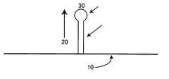
- the shape of a patterned element and the nature of the substratecan be selected to cause the catalyst sphere to form in substantially the center of the patterned element.
- the nanostructureis located in a region that is not substantially in the center of the area of the substrate initially covered by the patterned element, corresponding to the location of a predetermine position selected on the substrate (e.g., defined by a pit).
- the heating stepcan be performed before or after the adding step—that is, it is understood that the sphere optionally will be formed until after the precursors are added, e.g., where the presence of the precursor lowers the melting point causing the metal to melt and form the sphere.
- a “catalyst sphere”is not necessarily spherical in shape.
- a catalyst sphererefers to a single liquid drop of material comprising one or more nanostructure catalyst materials and one or more nanostructure precursors, where the shape of the drop is governed by the wetting properties of the liquid on the substrate, and/or the contact angle of the liquid on the substrate.
- the nanostructuresthemselves can include heterostructures or homostructures, which can be substantially uniform in diameter or substantially nonuniform in diameter.
- Arrays of nanostructures resulting from the methodare also a feature of the invention.
- an array of nanostructures comprising an arbitrary pattern of a plurality of nanostructures, each comprising a selected diameterare a feature of the invention.
- the individual characteristics of the nanostructures within the arrayare controlled, in part, by the individual features of the patterned elements from which they are formed.
- By creating an array of patterned elements with different sphere volumes, different materials and/or different shapesit is possible to form a predefined array of nanostructures with preselected characteristics of location, diameter and composition. It is also possible to form drops with a substantially geometric shape (e.g. square, hexagon, etc) through either the intrinsic crystal structure of the substrate, or active patterning of the substrate prior to metal deposition.
- nanostructures of the present inventionoptionally interact to form functional or operational elements such as LEDs, lasers, biosensors, logic circuits, memory, and/or the like.
- a patterned array of nanostructure catalystswith an almost unlimited set of parameters. These parameters can include the size and shape of each individual patterned element, the thickness of each individual patterned element, the material from which each individual patterned element is formed (e.g. including but not limited to gold, iron, cobalt, manganese, alloys, etc.). It is even possible, using standard lithographic processes, to create arrays of multiple different patterned materials, each from a different material. Each of these different patterned elements can be fabricated simultaneously or sequentially. It is possible to grow nanostructures from one array of patterned elements and then add additional patterned elements to the substrate to grow a second set of nanostructures.
- parameterscan include the size and shape of each individual patterned element, the thickness of each individual patterned element, the material from which each individual patterned element is formed (e.g. including but not limited to gold, iron, cobalt, manganese, alloys, etc.). It is even possible, using standard lithographic processes, to create arrays of multiple different patterned materials, each from a
- the nanostructures of the first and second setcan be made from either the same or different nanostructure precursors. It is also possible to remove any remaining catalyst/precursor spheres created in the first step prior to depositing the second set of patterned elements. This provides precise control over the material characteristics of the final nanostructure array.
- radiusis the same as the effective radius, defined as the average of the major and minor axes of the cross-section of the sphere at the interface with the substrate or nanostructure.
- sphere diametere.g. effective diameter
- patterned elementswith a surface area across the substrate that is much larger than the diameter of the resulting catalyst/precursor sphere.
- the thickness of the patterned elementwill be substantially smaller than the lateral dimensions of the element across the substrate.
- lithographic processeswith a resolution far larger than the defined diameter of the resulting nanostructures to create the array of patterned elements.
- a 50 nm diameter nanowirecan be formed from a circular patterned element with a diameter of 300 nm and a thickness of 7.4 nm. Note that these numbers are intended to emphasize a point, and that they do not necessarily represent the real numbers for an actual set of materials.
- the diameter of the resulting catalyst/precursor spherewill be modified by the additional volume resulting from the addition of the nanostructure precursor to the sphere.
- a magnetic fieldis applied to a eutectic interface between a nanostructure crystal and a catalyst mixture comprising a magnetic colloid (e.g., iron) and a nanostructure precursor.
- the catalyst mixturemay optionally comprise additional nonmetallic catalyst materials. This results in control over the direction or and diameter of nanostructure growth.
- a force that interacts with the catalyst colloide.g. a magnetic field
- the direction of the interface between the liquid and solidcan be modified and the direction of subsequent growth affected.
- the nanostructurewill tend to grow in a direction normal to the resulting interface.
- the resultwill be a deformation of the catalyst colloid, increasing or decreasing the effective diameter of the resulting sphere and therefore the resulting nanostructure.
- the methods of the present inventioncan be used to intentionally modify the diameter of the nanostructure during the growth process. Note that even forces that are directed non-normal to the existing interface can optionally change the effective diameter of the sphere.
- the magnetic fieldcan be, e.g., an electromagnetic grid, a grid of electro-magnets, a magnetic grid, or the like and the intensity or direction of the magnetic field can be altered during growth of the nanostructure.
- Resulting nanostructurescan be homostructures or heterostructures.
- the magnetic fieldcan be applied only at the beginning of the nanostructure growth process to influence the overall direction of the growth of a substantially straight nanostructure such as a substantially straight nanowire. This could be used to cause a catalyst colloid formed or placed at one electrode to grow a nanostructure substantially in the direction of a second electrode, even if no change in direction was applied after the growth process was started (i.e. after the first monolayer of the nanostructure was formed.
- Corresponding systemsare also a feature of the invention, e.g., a system comprising a nanowire crystal, a catalyst mixture comprising a magnetic colloid proximal to or in contact with the crystal, an electrical, magnetic, or electromagnetic field generator and a controller which directs orientation or intensity of a magnetic field produced by the magnetic field generator.
- the systemoptionally comprises a user interface which permits a user to direct the controller to direct the orientation or intensity of the magnetic field.
- the inventionincludes methods of making non-static (assemble-able and disassemble-able) arrays of nanostructures, such as nanowires, via fluidic control methods.
- at least a first set of nanostructuresis flowed into position to form a first array of nanostructures.
- more than one type of nanostructurecan comprise the set, e.g., a first type of nanostructure can be flowed from a first source and a second type of nanostructure can be flowed from a second source to provide the first set of nanostructures.
- first and second types of nanostructurescan be flowed from a single mixed source.
- nanostructure members of the first arraycan be the same or different (e.g., differ by size, composition, attachment of chemical or biological moieties, etc.) and can include homostructures or heterostructures.
- the nanostructures of the first arrayare reversibly immobilized in position.
- the first arraycan be a spatially ordered array, an individually addressable array, or a random array and members of the array can be in electrical contact with one another, or with external elements such as electrodes.
- the first array of nanostructuresis disassembled or moved by unimmobilizing the first set of nanostructures or the first array, or both. At least a second set of nanostructures is flowed into position to form a second array of nanostructures, which optionally includes any of the features noted for the first array.
- the nanostructures of the second arrayare immobilized in position, and this immobilization can be either reversible or irreversible.
- reversible immobilizationcan include one or more of: binding the nanostructures to a substrate via one or more reversible chemical bonds, applying fluidic pressure to the nanostructures, applying an electric field to the nanostructures, and/or applying a magnetic field to the nanostructures, using biological binding elements, covalent bonds or ionic bonds, and using electrostatic forces.
- the reversible immobilizationoptionally comprises individually locating and positioning (“individually addressing”) at least one of the nanostructures.
- nanostructuresare flowed into position within the arrays of nanostructures, it is not required that a flow be involved.
- nanostructuressuch as nanowires in solution are placed over the final location of the array and are transported to their final location by passive diffusion or active means such as electric or magnetic fields. This solution can be placed over the array location in a static drop, or the location of the final array can be immersed in the solution. It will be understood that any of the methods described here that do not explicitly require the force of fluidic movement for placement or alignment, can be repeated in a non-flow-based process using the methods of the present invention.
- Assayscan be performed using the first or second array, or both.
- the same assaycan be performed using the first array as using the second array, or different assays can be performed.
- one benefit of the non-static nature of the arraysis that assays that permanently alter an array (e.g., chemically modify or degrade the array) can desirably be performed using the non-static arrays, given that the arrays can be used once and then disassembled (that is, the arrays are optionally “single-use” arrays).
- An assay result detected using the arraycan include detecting a detectable signal such as an assay product mass, an assay product optical emission, an assay product electrical emission, a change in conductivity of the nanostructure array, an assay product magnetic field, and an assay product binding event, or the like.
- the methodsinclude flowing an electric current into or through the first or second array.
- the detectable signalcan also be generated by a secondary product of the assay product.
- an assay for mRNAcan be performed by measuring the detectable signal from a tRNA or DNA transcribed or reverse transcribed from the mRNA and still fall within the scope of the present invention.
- a protein fragment generated from a protein analytecan be used to quantify the presence of the original protein.
- the detectable productmay be an indirect product of the analyte.
- assay resultscan be determined by detecting any of changes described above for the enzyme product.
- binding elementssuch as aptazymes can be used that change configuration upon interaction with a specific analyte. The presence of the analyte then results in a change in the aptazyme, which, in turn, can be detected by the changes described above.
- any assaythat produces a quantitative or qualitative amount of a product in response to the presence of an analyte of interest can be detected using the methods described here. Such products are referred to as assay secondary products.
- the systemcan include a first source (well, chamber, microtiter tray, or the like) comprising at least a first suspension of nanostructures and a fluid conduit coupling the first suspension of nanostructures to a nanostructure array construction region.
- a first sourcewell, chamber, microtiter tray, or the like
- the systemcan be configured with multiple array assembly regions, multiple sources of nanostructures and fluidic conduit networks that couple the sources to the array assembly regions for the parallel assembly and disassembly of arrays.
- the array construction region(s)is/are configured to reversibly detain nanostructures from the first suspension such that the nanostructures in the suspensions are connected into an operable nanostructure array (or arrays).
- the systemoptionally includes a controller which regulates reversible detention of the nanostructures in the nanostructure array construction region(s).
- the systemoptionally includes a signal detector configured to be operably coupled to the array construction region(s) or to one or more nanostructure array(s) in the region(s). The signal detector detects, e.g., a mass signal, an optical signal, an electrical signal, a magnetic signal, a force signal, or a combination thereof, e.g., to detect an assay result or condition of the array.
- the signal detectorcan detect a signal from a single nanostructure (e.g., from a nanowire), or from multiple nanostructures simultaneously. These multiple nanostructures can be measured as a single measurement, or individually addressable, or some combination of the two.
- the systemoptionally includes a digital to analog or analog to digital converter (and A/D or D/A converter) which converts an analog signal from the signal detector into digital data.
- the systemoptionally includes a data storage module operably coupled to the signal detector, which stores signal data from the signal detector.
- the inventionprovides methods of performing an assay.
- at least a first set of nanostructures such as nanowiresis flowed into position to form a first array of nanostructures such as nanowires and an assay is performed.
- the assayproduces an assay result that is detectable by the first array and the assay result is detected.
- this aspectdoes not require non-static arrays, i.e., the array assembled by this method can be permanent or temporary. All of the various issues noted for arrays made via fluidic assembly methods apply equally to this embodiment.
- the assaysthat can be performed include detecting presence, concentration or relative concentration of a chemical or biological molecule, genotyping a sample, detecting a SNP, detecting an antigen, detecting an antibody, detecting a nucleic acid, detecting a protein, detecting a hazardous material, detecting a chemical or biological warfare agent, or the like.
- This embodimentcan be used to assemble an array of nanostructures immediately prior to running an assay, but can also be used to create a specific nanostructure array for an assay to be run in the future.
- the system comprising the as-assembled arraycan be packaged and shipped prior to running the assay.
- the present inventiondescribes a method of manufacturing a nanostructure array for use in a bioassay in which nanostructures such as nanowires with a specific assay binding element on their surface are flowed into position within an array and immobilized. This array is then later used to perform a bioassay.
- the nanostructurese.g., nanowires
- the binding elements on the surface of each wirecan either be the same or different within or between wires.
- This second alternativecan be done by taking advantage of compositional differences such as different chemically active groups on the surface of different nanostructures that are then used to bind to binding elements with specific complementary active groups.
- at least one of the nanostructuresis preferably in electrical contact with an electrode.
- some of the nanostructures/nanowiresare optionally individually addressable, and assay results from each assay type are determined by measuring a signal from a nanostructure with a binding element for that assay.
- the present inventionincludes methods of harvesting nanostructures.
- an etchable portion of the nanostructure or an etchable materiale.g., silicon oxide
- the nanostructurescan include heterostructure nanostructures, homostructure nanostructures, nanowires, nanotubes, nanorods, nanotetrapods, nanodots, nanoribbons quantum dots, or the like.
- the etchable materialcan be an etchable substrate.
- the substratecan comprise e.g., a layer of etchable material over a layer of a non-etchable material, or the etchable substrate can be etchable throughout.
- the etchable materialcan include an etchable attachment site to a substrate, or, e.g., an etchable region of the nanostructure that is differentially etchable from a non-etchable region of the nanostructure.
- the methodincludes etching a set of etchable portions, thereby releasing a set of nanostructures or, etching a set of etchable materials in contact with a set of nanostructures, thereby releasing the set of nanostructures.
- One or more etchantcan be used to release the nanostructures, e.g., a dry etchant, a wet-etchant, an isotropic etchant, an anisotrpic etchant a selective etchant, or the like.
- an etchable region of a nanostructurecan be located near the end of the nanostructure, before the catalyst colloid.
- etchingcan be used to cleanly remove the catalyst colloid from the nanostructure.
- etchable regionscan be located at both ends to cleanly release the nanostructure from both the substrate and the catalyst colloid.
- harvesting of nanostructures by the methods described hereresults in a substantially faceted end of the nanostructure where the etchable region was removed. This is in contrast to standard methods for harvesting nanostructures such as nanowires using sonication or the like, which result in a broken end.
- two or more etchable regions of a nanostructurecan be located at predefined distances from each other along the length of the nanostructure, so that, upon etching, the resulting nanostructure fragments are of a predefined length. If more than two etchable regions are included in each nanostructure, the spacing between the regions can be the same or different, and can be predefined or random to produce a plurality of different resulting nanostructure lengths.
- Corresponding systemsare also a feature of the invention, e.g., a system comprising at least one etchant, and at least one nanostructure comprising an etchable portion, or comprising one or more nanostructure coupled to an etchable material.
- the systemcan also include, e.g., an etchant controller which controls placement of the etchant onto the etchable portion or material, or which controls a duration of contact between the etchant and the etchable portion or material.
- the etchant controlleroptionally receives feedback from the system regarding the degree of etching achieved by the etchant and can control further contact of the etchant and the etchable portion or material in response to the feedback.
- the systemoptionally includes one or more etchant dispensing modules which dispense the etchant into contact with the etchable portion or material.
- the etchant dispensing modulesoptionally include one or more etchant flow channels or chambers which contain or direct flow of the etchant.
- feedbackcould involve direct measurement of the etchable material in the solution surrounding the nanostructure. The progress of etching can be measured by the rate of increase of concentration as a function of etching time, and the concentration of etchant can be adjusted to control the rate.
- methods of making one or more controlled length nanostructuresinclude depositing at least one nanostructure catalyst on a substrate and growing a nanostructure from the catalyst in a nanostructure growth process that comprises adding a first and a second material at different times during growth of the nanostructure, thereby controllably incorporating the first or second material, or both, into the nanostructure during the growth process.
- the resulting nanostructureis exposed to an etchant that differentially etches regions of the nanostructure made from the first or second material, thereby controllably cleaving the nanostructure into one or more controlled length nanostructures.
- the first or second materialcan comprise a dopant (e.g., the second material can be the first material plus a dopant).
- the methodwould include depositing at least one nanostructure catalyst on a substrate, growing a nanostructure from the catalyst in a nanostructure growth process that comprises periodically introducing one or more dopant during growth of the nanostructure, thereby controllably incorporating the dopant into the nanostructure during the growth process, and, exposing the resulting doped nanostructure to an etchant that differentially etches doped or non-doped regions of the doped nanostructure, thereby controllably cleaving the nanostructure into one or more controlled length nanostructures.
- the processcomprises periodically introducing a second material composition entirely, resulting in an alternating heterostructure of two materials, one of which is selected to be selectively etchable relative to the other.
- the substratecan include, e.g., a semiconducting crystalline material, a polymer, an amorphous surface, silicon, glass, quartz, alumina, gallium arsenide, or the like.
- the nanostructure catalystis optionally deposited lithographically, or, optionally, via controlled vapor deposition.
- the nanostructure catalystis typically deposited as a colloid that includes gold or another suitable catalyst (iron, silver, cobalt, etc) material.
- the nanostructure precursor or the dopantcan comprise, e.g., a group II, group III, group IV, group V, or group VI compound.
- the nanostructure precursorcan comprise silicon, while the dopant comprises B, P, As, Ge, Ga, In, or Al.
- the etchantcan include a dry etchant, a wet-etchant, an isotropic etchant, an anisotrpic etchant, a selective etchant, or the like.
- An example etchantcomprises NH 3 OH.
- the etchantselectively cleaves regions of the nanostructure comprising the dopant, or regions of the nanostructure that do not comprise the dopant, depending on the application.
- the nanostructureis cleaved such that the ends of the nanostructure comprise one or more dopant.
- the cleaved endsoptionally provide one or more conductive or semiconductive contact region for the nanostructure (which can be, e.g., a nanowire, a nanotube, a nanorod, a nanodot, or the like).
- a systemthat includes a substrate, a source of a nanostructure catalyst, system instructions for transporting the catalyst to the substrate and for depositing the nanostructure catalyst on the substrate, and a source of a nanostructure precursor are provided.
- the systemalso includes a source of a dopant material, system instructions for transporting the nanostructure precursors from the nanostructure precursor source to the substrate and into contact with deposited nanostructure catalyst, under conditions suitable for nanostructure growth, and system instructions for periodically introducing dopant from the dopant source to the substrate during growth of the nanostructure, thereby providing for controlled introduction of the dopant during growth of the nanostructure.
- the systemcan include a source of etchant that differentially etches doped or non-doped regions of the nanostructure, and instructions for introducing the etchant into contact with the nanostructure, thereby controllably cleaving the nanostructure into controlled length nanostructures.
- the substrate, nanostructure precursor, dopant or etchantcan be any of those previously noted and the nanostructure made in the system can be any of those previously noted as well.
- the catalyst source, the nanostructure precursor source, the dopant material source, or the etchant sourceoptionally comprises one or more gaseous or vapor materials containers.
- the system instructionsare typically embodied in a computer or in a computer readable media.
- this class of embodimentsincludes populations (including, optionally, arrays) of nanostructures comprising substantially similar lengths and dopant material composition, wherein the dopant material is heterogeneously distributed throughout the nanostructures.
- an array of nanostructurescomprising a substrate having a plurality of nanostructures projecting therefrom, wherein the nanostructures have dopant material similarly distributed in a plurality of regions of the nanostructures, wherein the distribution of the dopant material is non-uniform.
- the material composition of different nanostructuresis entirely different, rather than simply differing by dopant type.
- methods of making a nanostructure deviceare provided.
- a substrateis provided.
- a nanostructure catalyst particleis deposited on the substrate and a nanostructure is grown from the catalyst particle, providing a nanostructure with a catalyst particle at one end of the nanostructure.
- the end comprising the catalyst particleis then connected to one or more functional (e.g., electrical) contacts.
- Nanostructure devices made by the methodsare also a feature of the invention.
- the substrate in this class of embodimentscan include any of those noted above, e.g., a semiconducting crystalline material, a polymer, an amorphous surface, silicon, glass, quartz, alumina, gallium arsenide, or the like.
- the catalystcan be any of those noted herein, e.g., a gold particle.
- Depositing the nanostructure catalystoptionally includes etching the substrate, masking the etched substrate, and laying catalyst particles on the area accessible through the mask.
- the electrical contactsare coupled to each end of the nanostructure by planar processing, e.g., photolithography as in standard integrated circuit manufacturing.
- This set of embodimentsalso includes nanostructure devices.
- Example devicesinclude a substrate having a nanostructure thereon, wherein the nanostructure is coupled to a particle at least at one end of the nanostructure, wherein the particle is coupled to an electrical contact.
- the nanostructure deviceis optionally coupled to an electrical contact at each end of the nanostructure.
- the nanostructureis optionally oriented in a same plane as the substrate, or, in another desirable class of embodiments, is oriented perpendicular to the substrate. Arrays of such devices are also a feature of the invention.
- the inventionincludes methods of controlling growth of a nanostructure such as a nanowire.
- the methodincludes providing an electric field between two electrodes. Nanowire or other nanostructure growth is initiated at one or both of the electrodes by either forming the electrode from an appropriate catalytic material, or by incorporating a catalyst patterned element or colloid on the electrode. A nanostructure is then grown between the electrodes, with the electric field used to affect the direction of growth.
- the electric fielddirects nanostructure formation, e.g., by controlling the direction, orientation, and/or diameter of nanostructure formation.
- Electric-field directed growth of nanowires and nanotubesis know in the art; however, in the art, the electric field used to direct growth does not originate from the same electrodes that the wire is grown between.
- the magnitude of the electric fieldis modulated by a feedback mechanism that prevents a significant current from flowing through nanostructure after it bridges the gap between the electrodes.
- a change in current between the electrodes upon contact, or a change in capacitance between the electrodes during growthis detected, and the electric field is modified (e.g., reduced or turned off) in response to the nanostructure contact or the change in capacitance.
- the automatic detectionis performed with a circuit comprising a resistor.
- the systemcomprises a current-divider, as is known in the art, such that the relative resistance of a nanostructure is substantially larger than a second conducting path that the amount of current flow across the nanostructure at the voltages used for directed growth do not cause the nanostructure to break.
- This processcan be performed in parallel with multiple electrodes, e.g., by growing a plurality of additional nanostructures between a plurality of additional electrodes comprising nanostructure catalysts.
- the electric field or one or more additional electric fieldsdirect additional nanostructure growth between the additional electrodes.
- Nanostructure contact between the additional electrodesis automatically detected and the electric field or fields is modified in response to the contact.
- nanostructure contact between any two electrodescan be detected, e.g., by a series of resistors, e.g., one resistor per nanostructure.
- Extended contact by a nanostructure such as a nanowire to both electrodes while a potential difference exists between the electrodescan be undesirable, because the flow of current through the nanowire (or other relevant nanostructure) can burn out the nanowire if the flow is to high.
- detection of capacitancecan be used to shut the electric field off just prior to or approximately simultaneous with contact of a growing nanowire to a destination electrode. As the nanostructure grows toward the second electrode, the spacing between the electrodes decreases, and the capacitance decreases. This measurement can be calibrated as a direct measure of the remaining distance between the nanostructure and the second electrode.
- the nanostructurecan be grown for a period of time known to bridge enough of the gap between electrodes that the nanostructure will continue to grow in substantially the same direction, contacting the second electrode in the absence of an electric field. That way, the electric field can be turned off in the absence of any direct feedback.
- the nanostructuresare grown in the presence of a gate voltage, whereby the nanostructures are rendered non-conducting. As a result, the nanostructures act as insulators and no current flows upon connection with the second electrode.
- the systemsinclude a first electrode and a second electrode, where at least one of the electrodes comprises a nanostructure catalyst.
- the systemalso includes a nanostructure precursor, a power source coupled to the electrodes, a detector which detects nanostructure contact between the two electrodes or the progress of the growth of the nanostructure from one electrode to the other, and a controller which controls the power source in response to a signal from the detector.
- the power sourcecan be an AC or DC power source.
- the detector or controlleroptionally includes an electrical circuit that includes a resistor.
- the electrical circuitis coupled to the first electrode, the second electrode, or both the first and second electrodes. In one embodiment, the detector and the controller are provided by a single electrical circuit comprising a resistor.
- the electrical circuitis coupled to the first electrode, the second electrode, or both the first and second electrodes.
- the inventionincludes methods of making geometrically defined nanostructures.
- a nanostructure templateis seeded with a nanostructure catalyst (e.g., a particulate such as a gold or other metallic particulate).
- Nanostructuresare grown from or on the template, wherein the shape, direction, orientation or position of the nanostructures is constrained by the template.
- Systems for making geometrically defined nanostructuresare also a feature of the invention.
- the systemsinclude, e.g., a template seeded with a nanostructure catalyst and, a nanostructure precursor.
- the nanostructure templatecan include wells, pits, trenches, channels or grooves into which the catalyst is seeded.
- the nanostructure templateincludes a shaped region (e.g., produced by laser ablation or etching) into which the catalyst is seeded.
- the shaped regionscan be evenly or irregularly spaced.
- the nanostructures produced by these methods and systemsoptionally include heterostructure nanostructures or homostructure nanostructures.
- the templatecan be used to define the origination point of a growing nanostructure by localizing the catalyst material (e.g. in a pit).
- the templatecan also influence the direction of the growth. For instance, a catalyst placed at the end of a long narrow trench is forced to grow along the trench, unless some force causes it to grow in a direction that takes it outside of the trench. This can be prevented by using a substrate that is substantially amorphous under the growth conditions for the wires. In that case, the wires generally grow isotropically along the surface of the substrate. Alternatively, the wires can be grown in a channel that is closed on all sides, with precursors flowed in from the end.
- a templatecould be created with a trench extending from one electrode to another.
- the trenchshould have an aspect ratio of greater than 10:1, and preferably be less than 1 micron wide.
- a catalyst placed on one electrode at one end of the trenchwill begin to grow a nanostructure.
- the direction of that growthcan be influence by an electric or magnetic field, or not be influenced at all.
- the walls of the trench, acting as barriers to growth in 3 of 4 possible growth directions,causes the wire to grow in a direction substantially toward the second electrode. This channel can be straight or bent, and/or can intersect other channels.
- crossed channelscan be used to create cross-bar structures between several nanostructures that can be grown either simultaneously or sequentially.
- the present inventionincludes methods of depositing nanostructures such as nanowires on a substrate.
- nanostructuresare suspended in solution.
- the resulting nanostructure suspensionis applied to a rotatable substrate which is rotated, thereby depositing the nanostructures on the rotating rotatable substrate.
- Thishas the advantage of radially aligning the nanostructures on the rotatable substrate.
- the nanostructuresare optionally applied to the rotatable substrate prior to rotation of the rotatable substrate, or alternately can be applied to the rotatable substrate during rotation of the rotatable substrate.
- the nanostructures which are radially alignedcan comprise heterostructures or homostructure nanostructures.
- the substrateis optionally chemically functionalized to bind to the nanostructures, securing them in position once they contact the surface.
- Corresponding systems for radially aligning nanostructurescan also be produced.
- the systemsinclude a rotatable substrate adapted to receive nanostructures, a rotation mechanism which is configured to rotate the rotatable substrate and a suspension of nanostructures.
- the systemalso optionally includes a contact module which contacts the suspension of nanostructures to the rotatable substrate.
- the inventionincludes a large scale method of nanostructure (e.g., nanowire) production.
- the methodincludes providing a particulate nanostructure catalyst to a fluid or aerosol reactor and growing nanostructures from the particulate catalysts.
- Corresponding systemsare also a feature of the invention, e.g., which include a particulate nanostructure catalyst, a fluid or aerosol reaction chamber and a nanostructure precursor.
- the nanostructures that are providedinclude heterostructure nanostructures, homostructure nanostructures and/or the like.
- methods of making nanostructuresinclude entrapping a nanostructure catalyst in a flowing gas or plasma stream, contacting the nanostructure catalyst with one or more nanostructure precursors, whereby the nanostructures are formed in the flowing gas or plasma stream, and extracting the nanostructures from the flowing gas or plasma stream.
- the nanostructure catalystis typically a colloid, e.g., a gold colloid solution.
- the gastypically comprises one or more noble gas, e.g., He or Ar.
- the nanostructure catalystis optionally entrapped in the gas stream, which is converted into a plasma stream prior to contacting the nanostructure precursors to the catalysts in the resulting plasma stream, e.g., by exposing the stream to a radio frequency or microwave field.
- the catalystis optionally entrapped in the gas stream by pulsing a catalyst target with a laser, thereby vaporizing a portion of the catalyst target and releasing catalyst into the gas stream.
- the catalystis optionally on a movable (e.g., motorized) stage that is moved to provide release of a regulated, e.g., constant, amount of catalyst by the laser.
- the laseris optionally controlled by a feedback loop, also to assist in regulating release of catalyst.
- the nanostructure precursortypically comprises a group II, group II, group IV, group V, or group VI compound, e.g., silicon.
- the nanostructure precursoroptionally comprises a dopant, e.g., any of those noted herein.
- the nanostructures producedare any of those noted herein.
- nanostructure precursorsare introduced into the flowing stream before, during or after introduction of the catalyst.
- nanowire precursorsare optionally preheated in the flowing gas stream before contacting the catalyst.
- the precursorsoptionally contact the catalyst in a reaction chamber in which the catalyst is released from a catalyst target by pulsing the target with a laser.
- the catalystis optionally entrapped in a gas stream and converted into a plasma by flowing the gas stream through a radio frequency or microwave field.
- the precursoris optionally entrapped in an additional gas stream that is preheated prior to being exposed to the plasma in a reaction chamber.
- the extractionoptionally includes condensing the nanostructures on a cold substrate.
- the methodalso optionally includes extracting gas or plasma downstream of a site where the nanostructures are extracted.
- the gas or plasmais optionally scrubbed.
- a continuous phase nanostructure synthesis systemincludes a gas or plasma source, a nanostructure synthesis region, and a flow path that permits flow of gas or plasma from the gas or plasma source to the nanostructure synthesis region.
- the systemalso includes a nanostructure catalyst source coupled to the synthesis region, a nanostructure precursor source coupled to the synthesis region, and a nanostructure extraction site coupled to the synthesis region.
- the systemincludes a gas or plasma extraction region downstream of the synthesis region, configured to flow gas from the gas source to the gas extraction region during synthesis of the nanostructure in the synthesis region.
- the gas or plasma sourceoptionally comprises a noble gas source, e.g., an He source or an Ar source.
- the plasma sourceis optionally coupled to a gas source, wherein a gas is flowed from the gas source through a radio frequency or microwave field to produce the plasma.
- the nanostructure catalyst, precursor and dopantcan be any of those noted above.
- the nanostructure synthesis regioncomprises a target that comprises the catalyst.
- the systemalso optionally comprises a laser that releases the catalyst from the target during operation of the system.
- the laseroptionally comprises a control loop that pulses the laser and a laser energy meter which are used to regulate the about of catalyst released from the target.
- the targetis optionally motorized, permitting movement of the target relative to the laser and concomitant regulation of catalyst release from the target.
- the flow pathoptionally comprises a gas preheater that preheats the gas prior to flow of the gas to the nanostructure synthesis region.
- An additional gas source and an additional flow path from the additional gas source to the synthesis regioncan also be incorporated into the system, along with a preheater that preheats gas in the additional flow path.
- the precursor sourceis optionally coupled to the additional gas source and the system optionally includes system instructions that direct the precursor to be flowed through the preheater prior to delivery of the precursor to the nanostructure synthesis region.
- the gas or plasma sourceis optionally coupled to the catalyst source and the system optionally includes system instructions that direct the catalyst to be flowed into the synthesis region.
- the nanostructure extraction sitetypically includes a substrate that is sufficiently cold to condense gas or plasma comprising a nanostructure onto the substrate.
- the gas or plasma extraction regionoptionally comprises a scrubber that scrubs the gas or plasma to remove nanostructures from the gas or plasma.
- Another class of embodimentsrelates to methods of functionalizing nanostructures, including any of those made by any of the preceding methods.
- methods of making a functionalized nanostructure or nanostructure precursorare provided.
- the methodsinclude treating the nanostructure or precursor with a functionalizing plasma, whereby a functional group is attached to the precursor or nanostructure.
- Any suitable functionalizing chemistrycan be used in this process, including, e.g., where the functionalizing plasma comprises ammonia, nitrogen, a primary amine, or hydrogen.
- the precursoris optionally subsequently incorporated into a nanostructure.
- Nanostructures made according to these methodsare also a feature of the invention.
- a plasma that includes a functionalizing precursor and a nanostructure precursor or a nanostructureis also a feature of the invention.
- a nanostructure comprising a functionalized outer surface, e.g., a nitride layeris a feature of the invention.
- the functional groupis attached to the outer surface of the nanostructure. This can provide an insulating layer on the nanostructure and/or a site for chemical attachment of additional moieties.
- Kitscomprising any of the above nanostructures, devices, arrays, systems or the like, e.g., comprising instructions for the use of the nanostructures, devices, arrays, systems in the methods herein are also a feature of the invention. Kits optionally further include end use features, containers for storing other components of the kit, packaging materials and the like.
- An “array” of nanostructuresis an assemblage of nanostructures.
- the assemblagecan be spatially ordered (a “patterned array”) or disordered (a “randomly patterned” array).
- the arraycan form or comprise one or more functional elements (e.g., a junction or collection of junctions) or can be non-functional.
- a “functional element”is a component of a circuit, device, detector, or system. Examples include wires, current paths, transistors, diodes, rectifiers, amplifiers, and many others known to one of skill.
- a “nanostructure”is a structure having at least one region or characteristic dimension with a dimension of less than 500 nm, e.g., less than 200 nm, less than 100 nm, less than 50 nm, or even less than 20 nm. In many cases, the region or characteristic dimension will be along the smallest axis of the structure.
- a conductive or semi-conductive nanostructureoften displays 1-dimensional quantum confinement, e.g., an electron can often travel along only one dimension of the structure. Examples of nanostructures include nanowires, nanotubes, nanodots, nanorods, nanotetrapods, quantum dots, nanoribbons and the like.
- a “homonanostructure”is a nanostructure that has an essentially homogeneous arrangement of constituent elements.
- a homonanowireis a homonanostructure that can be a substantially single crystal structure comprising a base material such as silicon and, optionally, a dopant dispersed in essentially the same manner throughout the crystal.
- a “heteronanostructure”is a nanostructure that includes subdomains comprising different compositions.
- a heteronanowireis a heteronanostructure that can be a single crystal structure comprising a base material such as silicon with different subdomains or “segments” having different dopants, or different concentrations of one dopant, or an entirely different material, or any combination thereof.
- the nanostructures of the inventiontypically have an aspect ratio greater than 5, typically greater than 10, generally greater than 50, and, optionally, greater than 100 or more.
- a “nanowire”is an elongated nanostructure having at least one cross sectional dimension that is less than about 500 nm e.g., less than about 200 nm, less than about 100 nm, less than about 50 nm, or even less than about 20 nm or less, and has an aspect ratio (e.g., length:width) of greater than about 10, preferably, greater than about 50, and more preferably, greater than about 100.
- a nanowireis optionally substantially single crystal in structure (a “single crystal nanowire” or a “monocrystalline nanowire”). It is optionally conductive or semiconductive.
- a “homonanowire”is a nanowire that has an essentially homogeneous arrangement of constituent elements.
- a homonanowirecan be a single crystal structure comprising a base material such as silicon and a dopant dispersed in essentially the same manner throughout the crystal.
- a “heteronanowire”is a nanowire that includes subdomains comprising different compositions.
- a heteronanowirecan be a single crystal structure comprising a base material such as silicon, with different subdomains or “segments” having different dopants, or different concentrations of one dopant, or both.
- nanowiresinclude semiconductor nanowires as described in Published International Patent Application Nos. WO 02/17362, WO 02/48701, and 01/03208, carbon nanotubes, and other elongated conductive or semiconductive structures of like dimensions.
- nanowiresinclude semiconductive nanowires, e.g., those that are comprised of semiconductor material selected from, e.g., Si, Ge, Sn, Se, Te, B, Diamond, P, B—C, B—P(BP6), B—Si, Si—C, Si—Ge, Si—Sn and Ge—Sn, SiC, BN/BP/BAs, AlN/AlP/AlAs/AlSb, GaN/GaP/GaAs/GaSb, InN/InP/InAs/InSb, BN/BP/BAs, AlN/AIP/AlAs/AlSb, GaN/GaP/GaAs/GaSb, InN/InP/InAs/InSb, ZnO/ZnS/ZnSe/ZnTe, CdS/CdSe/CdTe, HgS/HgSe/HgTe, BeS/BeSe/
- the semiconductormay comprise a dopant from a group consisting of: a p-type dopant from Group III of the periodic table; an n-type dopant from Group V of the periodic table; a p-type dopant selected from a group consisting of: B, Al and In; an n-type dopant selected from a group consisting of: P, As and Sb; a p-type dopant from Group II of the periodic table; a p-type dopant selected from a group consisting of: Mg, Zn, Cd and Hg; a p-type dopant from Group IV of the periodic table; a p-type dopant selected from a group consisting of: C and Si.; or an n-type is selected from a group consisting of: Si, Ge, Sn, S, Se and Te.
- substantially single crystalrefers to a structure that has long-range order over at least 100 nm in at least 1 dimension within the structure. It will be understood that a substantially single crystal nanowire may contain defects or stacking faults and still be referred to as substantially single crystal as long as long-range order is present.
- the surface of a nanowirecan be either single crystalline, polycrystalline or amorphous without affecting the description of the overall nanowire as being substantially single crystal.
- the nanowireis considered to be single crystal if it comprises a substantially single crystal core extending radially from the center of the wire more than 1 ⁇ 5 of the distance to the surface, preferably 1 ⁇ 2 of the way to the surface.
- a “controlled length nanostructure”is a nanostructure produced under conditions that regulate, in a controlled or controllable manner, the length of the nanostructure produced.
- nanostructure catalystis a material that facilitates the formation or growth of a nanostructure.
- colloidssuch as gold act as nanostructure catalysts.
- FIG. 1is a schematic of a nanostructure growing from a substrate.
- FIG. 2is a schematic of a graph of time-controlled dopant introduction, and a resulting nanostructure.
- FIG. 3is a schematic of cleavage of a nanostructure.
- FIG. 4is a schematic of a continuous reactor for producing nanostructures.
- FIG. 5is a schematic of a continuous reactor for producing nanostructures.
- FIG. 6is a schematic of a continuous reactor for producing nanostructures.
- FIG. 7schematically illustrates a nanostructure on a substrate.
- FIG. 8schematically illustrates a system for planar processing of a nanostructure.
- FIG. 9schematically illustrates formation of an array of catalyst particles via patterning with a resist.
- FIG. 10schematically illustrates alteration of nanostructure growth upon application of a magnetic field.
- the present inventionprovides a variety of methods of making and arranging nanostructures such as nanowires, e.g., into functional devices, arrays or device or array components.
- the following discussionfocuses first on the formation of nanostructures and nanostructure arrays via patterning, then focuses on oriented growth in magnetic fields and then on fluidic assembly of nanostructure arrays.
- Harvesting of nanostructures from a substrate via etching (including use of etch planes for making nanostructures such as nanowires with defined ends and/or controlled lengths) and manufacturing of nanostructures on substrates and integration with IC by planar processing methodsis then covered.
- Power directed orientation and growth of nanostructures, template directed nanostructures growth and radial nanostructures depositionare addressed.
- Large scale growth of nanostructurese.g., by continuous gas and plasma phase synthesis approaches are then covered, followed by nanostructure functionalization via functionalizing plasmas. Integration of nanowires into biosensors and device elements is then addressed.
- synthesis methods hereincan be used to make nanostructures used in any of the ordering approaches herein.
- methods of modifying nanostructures, e.g., via functionalizing plasmasare also described and can be applied to any of the manufacturing or array/device approaches herein.
- Various methods of making nanostructures, device components and whole devices (e.g., biosensors) using the methods hereinare also discussed.
- nanostructurese.g., nanowires
- any other small/1-dimensional componentsuch as nanowires, nanodots, nanotubes, nanoribbons, nanotetrapods, quantum dots or the like can be made/ordered/arranged using the methods and systems herein.
- certain structures that can fall outside of the definition of nanostructures, such as semiconductor whiskers,can also be assembled/ordered/produced by the methods herein.
- the present inventionprovides methods of forming nanowires (or any other small or one-dimensional structure, e.g., a nanodot, nanoribbon, nanotetrapod, etc.) and corresponding arrays with any of a variety of properties by patterning nanostructure catalysts and/or precursors on a substrate. Nanostructure catalysts and/or precursors are heated, melting into spheres that influence the eventual diameter and location of nanostructures made from the spheres.
- the nanowires or other structures produced by the methodscan be homostructures (homonanowires), heterostructures (heteronanowire) and can be formed into functional or non-functional elements.
- the wirescan form junctions, transistors, field effect transistors, amplifiers, circuits, diodes, gates, emitters, collectors, p-type gates, sensors, memory, or the like, or can be simple arrays of nanowires.
- FIG. 9Patterning of a catalyst on a substrate is illustrated in FIG. 9 .
- substrate 904e.g., a silicon wafer
- coating 903e.g., silicon dioxide
- catalyst 901e.g., gold
- panel Bcatalyst 901 is lifted off by removing resist 902 .
- the catalystis then reformed, e.g., via heating to form spheres ( 9 C).
- a nanostructure catalystis patterned on a substrate in a plurality of patterned elements.
- the patterned elementsare typically of a thickness and shape such that a corresponding sphere diameter for the patterned element is less than a selected nanostructure (upon addition of nanowire catalyst, the sphere volume becomes approximately equal to the selected nanostructure, e.g., nanowire).
- the sphere diameteris actually the effective diameter of a liquid drop, with the wetting-characteristics of the materials used in contact with the substrate surface.
- the catalystcan be essentially any nanostructure catalyst material, e.g., a metal. Examples of suitable materials include gold, iron, cobalt, manganese and sliver.
- nanostructure catalystis heated to form nanostructure catalyst spheres and nanostructure precursors are added to form spheres of catalyst and precursor (generally, the addition of the precursors is performed at approximately the same time as the catalyst is heated, though the catalyst or the precursor can be added before or after the heating step). Alternatively, the catalyst can be heated prior to addition of the precursor and precursor addition can occur prior to sphere formation. Nanostructures are then formed from the catalyst/precursor spheres.
- the shape and thickness of the patterned elements and the interaction of the element constituents with the substratedetermine droplet formation characteristics of the catalyst and catalyst/precursor materials.
- the shape and thickness of the elementsis selected to provide any desired drop formation characteristics.
- the patterned elementsare simply formed as disks, but any other geometric shape can be used, as long as the thickness and shape provide for droplet formation.
- the parameters for shape formationinclude surface tension of melted catalyst/precursor components, friction between the melted catalyst/precursor components and the substrate, gravity, the presence or absence of centripetal forces and the like.
- the methodoptionally includes a step of selecting a desired nanostructure diameter and selecting a corresponding sphere diameter to determine the desired nanostructure diameter.
- the sphere diametercan be selected in part by empirically determining droplet formation characteristics of the nanostructure catalyst on a selected surface. Droplet formation is controlled by controlling lateral or thickness dimensions, or both, of the patterned elements.
- the methodoptionally includes selecting thickness or surface dimensions of the patterned elements to control sphere formation.
- the methodoptionally includes selecting a plurality of desired nanostructure diameters, selecting a plurality of sphere diameters to equal the plurality of desired nanostructure (e.g., nanowire) diameters, and depositing a plurality of patterned elements to generate that plurality of sphere diameters.
- Sphere formationcan optionally be controlled by controlling the rate of heating and the rate of precursor addition.
- the patterned elementsaggregate into single droplets when heated in the presence of the nanostructure precursors.
- the formation of single dropletsprovides better sphere size control than patterning element that break into multiple droplets ⁇ although this later approach can be used as well, e.g., where the size of nanostructures grown from spheres can vary in the application of interest.
- Parameterssuch as temperature, rate of temperature change, presence or absence of nanostructure precursor gasses during or prior to heating, as well as timing and rate of precursor introduction and relative rates of different precursor components in binary and higher-order materials all be used to control the formation of droplets and promote single-drop vs multi-drop formation.
- the substratecan be pre-patterned in such a way as to promote droplet formation in specific locations on the substrate. This can be done with patterned catalyst that coats the entire substrate, or just covers the patterned locations.
- patterned catalystthat coats the entire substrate, or just covers the patterned locations.
- One example of patterningcould be an etched pit (or pinhole) that creates a high-surface tension at on location on the substrate and promotes aggregation of the melted catalyst at that location.
- this processcan be used to control the size and density of catalyst drops that form on a surface. This can be either periodic or non-periodic.
- the single dropletscan be substantially uniform in size, or not substantially uniform in size across an array.
- the distribution of sizes of patterned elementscan vary in a selected fashion, e.g., in a manner that is not simply the result of manufacturing variation.
- the usercan select to place nanostructures of any diameter in any location by placing patterned elements with appropriate characteristics in those locations.
- the size of the patterned elementscan display a non-Gaussian size distribution.
- the patterned elementsaggregate into single droplets that display a bimodal volume distribution. Where 3 sizes are desirable, the patterned elements aggregate into single droplets that display at a trimodal volume distribution.
- the number of desired sizes in the final application (n)will lead to an n-modal volume distribution of droplets and a corresponding n-modal size/shape/thickness distribution of patterned elements.
- the nanostructure catalyst/precursor spheresform an array of droplets, from which an array of nanostructures are grown.
- the arraycan be a regularly ordered array or an irregular array, depending on the intended application.
- the nanostructures or other components of the arraycan be homostructure or heterostructure elements, also depending on the intended application.
- nanowirescan be of a substantially uniform diameter, or can be of varying (non-uniform) diameter.
- the nanowirescan comprise silicon or other materials, and can be doped or non-doped. The precise size, array arrangement and composition of the array and nanostructures within the array are dependent on the application to which the array is to be put.
- Applications of this technologyinclude, but are not limited to, cold-cathodes, field-emission arrays, laser diodes arrays, LED arrays, solid adhesives, thermoelectric coolers, thermo-generators, photovoltaic cells, transistor arrays, biosensor arrays, and the like.
- the catalyst materials which are patterned on the substratecan be essentially anything that can function as a nanostructure catalyst, e.g., a gold, iron, etc. catalyst.
- the array of patterned catalyst elementscan include one or more than one catalysts component. These components can be separated into different elements in the array (e.g., one patterned element optionally includes gold while another includes iron), or can be combined into a single patterned element (e.g., a patterned element can include gold, or iron, or both gold and iron).
- the patterned elementsoptionally differ in volume. Patterned elements that differ in volume or composition can be patterned sequentially or simultaneously.
- the various steps of the methodscan also be performed recursively, e.g., by repeating patterning, catalyst/precursor addition/heating steps performed on a first set of nanostructure catalysts/precursors on a second set of nanostructure catalysts/precursors.
- This cyclecan be performed as many times as desired, until the array achieves a desired complexity.
- This ability to increase array complexity by patterning different types of nanostructures into the array during different rounds of nanostructure assemblypermits the formation of highly complex arrays.
- Thiscan be done by selective etching, for example with an acidic etchant, to remove the metal catalysts over the semiconductor nanostructures (in another embodiment, the nanostructure can simply be etched below the catalyst, e.g., by incorporating an appropriate selectively etchable material into the nanostructure, as described in more detail herein).
- etch planes to provide uniform wire cleavage pointsis described below in more detail and can be performed in this application.
- thermoelectric deviceswhere one desires both n- and p-doped thermoelectric channels, to provided for running heating and/or cooling in parallel on the same substrate.
- the patterned elements that differ in volume or compositioncan be formed into functional components, e.g., by crossing component types in the arrays. That is, a first type of nanostructure can be formed in one region of the array, with a second type of nanostructure being formed in another region of the array. These regions can intersect to provide functional elements through the interaction of different types of nanostructures.
- the nanostructurescan interact to form functional elements such as a transistor, an LED, a laser, a biosensor, a logic circuit, memory, a heating or cooling element, and/or the like.
- arrays of nanostructures having an arbitrary (e.g., a selected) pattern of a plurality of nanostructures, each nanostructure having a given (e.g., selected) diameterare a feature of the invention.
- the arbitrary patterncan be a randomly or non-randomly selected pattern.
- the nanostructures of the arraycan be the same or different, and can comprise heterostructure or homostructure nanostructures.
- the nanostructurescan be substantially uniform or non-uniform in diameter.
- the nanostructurescan differ or be the same with respect to composition, size uniformity, spacing in the array, or the like.
- the arrayscan form functional or non-functional elements (e.g., can form one or more of: an LED, a laser, a biosensor, a logic circuit, and/or memory).
- the inventionprovides a patterned array of nanostructure catalyst elements on a substrate, where a volume of a plurality of the patterned elements has a sphere diameter less than a nanostructure.
- the diameter of the sphere volume corresponding to the patterned catalyst elementsis less than the diameter of the nanostructure, because, in general, the volume of the patterned catalyst elements plus the nanostructure precursors determines the nanostructure diameter.
- the patterned elementscan include elements which differ in size or composition as noted above.
- the patterned elementscan be patterned in any suitable catalyst material, e.g., colloidal gold, iron, or the like.
- a first set of patterned elementscomprises gold and a second set of elements comprises iron.
- the patterned elementswill generally include the catalyst(s) of interest and optionally include the precursors.
- the nanostructure precursorscan be added after the catalysts are patterned on the substrate.
- the nanostructure precursorsare patterned on the substrate and the catalysts are added to the patterned precursors. In any case, the various principles noted above can be applied.
- the spheres formed from the patterned elements and any added componentscan also differ in size or composition as noted above.
- the inventionalso provides an array of nanowire catalyst/nanowire precursor spheres on a substrate, where a volume of a plurality of the spheres have sphere diameters approximately equal to a nanowire.
- the present inventionprovides a variety of methods of orienting and directing nanostructure growth which can be applied in a number of the other embodiments herein.
- methods of growing nanowires in a selected direction or orientationare provided, in which a magnetic field is applied to a eutectic interface between a nanowire crystal and a catalyst mixture comprising a magnetic colloid and a nanowire precursor.
- a variety of ways of generating the magnetic fieldcan be used, e.g., via an electromagnetic grid, an electromagnet grid, a magnetic grid, or the like. That is, the magnetic field can comprise or be produced using any of these components.
- the methodoptionally includes altering the direction of the magnetic field during growth of the nanowire, thereby influencing the direction or orientation of nanowire growth.
- FIG. 10This embodiment is further illustrated in FIG. 10 .
- growth of a nanostructure in the absence of a magnetic fieldis upwards (in this example).
- application of a magnetic field(illustrated by arrows) results in growth in the direction of the magnetic field.
- the nanostructuresare shown with a catalyst cap.
- the colloidcan include magnetic materials such as iron.
- the precursorcan include any appropriate nanowire precursor material, such as silicon, doped silicon or the like.
- the product nanowires of the methodscan include heterostructure nanowires, homostructure nanowires, or both.
- systems for practicing the methodsare also a feature of the invention.
- systemscan include a nanowire crystal, a catalyst mixture comprising a magnetic colloid proximal to or in contact with the crystal, an electrical, magnetic, or electromagnetic field generator and a controller which directs orientation or intensity of a magnetic field produced by the magnetic field generator.
- the systemsalso optionally include additional features such as a user interface which permits a user to direct the controller to direct the orientation or intensity of the magnetic field.
- the methods of the inventioninclude making arrays by flowing nanostructures into contact with one another.
- the nanostructurescan be individually addressable, with each nanostructure captured in a particular position and/or orientation in a particular region, or the assembly can be addressed via group capture methods (or even via stochastic assembly).
- the composition of an individually addressed array of nanostructurescan be predetermined, such that the presence of a selected nanostructure at each position in the individually addressable array is pre-selected. Alternately, the presence of a selected nanostructure from a nanostructure set or suspension at each position in the individually addressable array can be not pre-selected.
- the methodcan include determining which nanostructures are positioned in which positions in the individually addressable array. For example, position can be determined by detecting one or more property of each of the nanostructures and comparing the property to a nanostructure property look-up table.
- One arrangement for capturing nanostructuresinvolves forming surfaces that comprise regions that selectively attract nanostructures.
- —NH 2can be presented in a particular pattern at a surface, and that pattern will attract nanowires or nanotubes having surface functionality attractive to amines.
- Surfacescan be patterned using known techniques such as electron-beam patterning, soft-lithography, or the like. See also, International Patent Publication No. WO 96/29629, published Jul. 26, 1996, and U.S. Pat. No. 5,512,131, issued Apr. 30, 1996.
- assaysare performed using the nanostructure arrays.
- the nanostructuresare released following use and fresh nanostructures can be flowed into position to form additional nanostructure arrays.
- array construction/deconstructioncan be performed in real time as compared to the assays that are run using the arrays.
- This ability to quickly assemble and disassemble nanostructure arrays, in any desired configurationprovides many advantages, particularly when the arrays can be used only once in the assay at issue. For example, many assays involve irreversible binding of materials to the nanostructures, which prevents further use of the nanostructure array in the assay at issue.
- the inventionincludes methods of performing an assay in which at least a first set of nanostructures is flowed into position to form a first array of nanostructures, performing an assay, which produces an assay result that is detectable by the first array, and, detecting the assay result.
- the nanostructures which are flowed into positioncan be reversibly or irreversibly positioned in place.
- the assaycomprises irreversible binding of an analyte to at least one member of the first set of nanostructures
- methods of making arrays of nanostructuresare provided in which at least a first set of nanostructures is flowed into position to form a first array of nanostructures, where the nanostructures of the first array are reversibly immobilized in position.
- the first array of nanostructuresis then disassembled or moved by unimmobilizing the first set of nanostructures, or the first array, or both.
- At least a second set of nanostructuresis flowed into position to form a second array of nanostructures, where the nanostructures of the second array are reversibly immobilized in position.
- the reversible immobilizationcan include any method of achieving reversible binding, e.g., binding the nanostructures to a substrate via one or more reversible chemical bonds, applying fluidic pressure to the nanostructures, applying an electric field to the nanostructures, and/or applying a magnetic field to the nanostructures, or the like.
- the reversible immobilizationoptionally includes individually locating and positioning at least one of the nanostructure, e.g., where the members of an array are “individually addressable.”
- the members of the arrayare not individually positioned, but are, instead, positioned as nanostructure types or other nanostructure sets, e.g., by capturing groups that share a common feature (e.g., a size dimension, presence of a capture moiety (e.g., a magnetic or ferric particle, an antibody or the like), and/or that are released or flowed as a group in the fluidic system.
- a common featuree.g., a size dimension, presence of a capture moiety (e.g., a magnetic or ferric particle, an antibody or the like)
- a capture moietye.g., a magnetic or ferric particle, an antibody or the like
- the arraysare most typically spatially ordered arrays, e.g., assemblies of nanostructures that form regularly spaced components.
- the arrayscan be randomly ordered, or can include randomly ordered regions, e.g., show a random spatial pattern of assembly.
- Different types of nanostructurescan be flowed from different sources of the nanostructures to form the arrays, e.g., where the nanostructures are flowed from fluidic suspensions of different types of nanostructures.
- a first type of nanostructureis flowed from a first source and a second type of nanostructure is flowed from a second source to provide a set (e.g., the first or second set noted above) or an assemblage (e.g., array) of nanostructures.
- the arrays which are assembledcan include more than one type of nanostructure, e.g., where assemblies of nanowires provide a functional element such as an assay element.
- the arraycan comprise semiconducting nanowires such as n-type semiconducting nanowires and/or p-type semiconducting nanowires.
- device elementssuch as diodes, rectifiers, transistors, amplifiers and the like, can be constructed from p-n or various p-n combination (e.g., pnp, npn, pin, pip, etc.) junctions.
- the nanowires or other structures which are assembled into arraysare optionally doped, e.g., in a conventional manner using conventional dopants such as B, P, As, Ga, In and/or Al.
- Both the nanowire or other nanostructure materials and the dopant materialscan be selected from, e.g., Groups II, III, IV, V, VI, etc., and can include quaternaries and tertiaries, as well as oxides.
- Different nanostructure semiconductor typescan be assembled by the methods herein, e.g., group III-V semiconductor nanowires, group II-VI semiconductor nanowires, group II-IV semiconductor nanowires, etc.
- Nanowirescan be homonanowires (having the same basic structure throughout) or heteronanowires (having regions of different structure, e.g., regions which differ by dopant).
- the nanowirescan comprise molecules permanently or temporarily attached to the surface of the nanowires.
- the first or second sets of nanowires noted aboveare optionally attached to the same or to different chemical or biological moieties.
- the nanowires of the arrays which are assembled by this methodcan differ or be the same with respect to properties (e.g., semiconducting vs. conducting or non-conducting), presence, absence or type of dopants, presence, absence or type of bound moieties (chemical, biological, structural, etc.), basic composition, or the like.
- the plurality of nanostructure members of the first or second or any subsequently assembled arrayare optionally in electrical contact with each other.
- This electrical contactcan be any type of electrical contact, whether direct or indirect.
- the arrays of the inventioncan be used to perform one or more assay of interest.
- one or more assaycan be performed on or with the first array and the results of the assay detected, followed by flowing the second set of nanostructures into position and performing an assay on or with the second array. This process can be repeated until the source of nanostructures is depleted (and, of course, the source can be replenished (or continuously replenished) and the process continued as desired.
- the assay resultscan comprise a detectable signal such as product mass (e.g., the mass of an assay product can be detected on the array), an optical emission (e.g., emission of light, e.g., a fluorescent or luminescent emission), an electrical emission from the array, a change in conductivity of the nanostructure array, an magnetic field produced by a product (e.g., captured by the array), a product binding event (e.g., binding of an antibody or antigen to the array), or the like.
- detection modalitiescan include flowing an electric current into or proximal to the first or second array, detecting an optical signal, or the like.
- the different arrays that are constructed in by the fluidic systemcan be used to perform the same or different assays and, thus, can involve detection of the same type of signal or of different signal types.
- a system of the inventioncan include a first source comprising a first suspension of nanostructures as noted above.
- the systemcan also include a fluid conduit (e.g., a channel or channel network, e.g., a microfluidic channel or channel network) coupling the first suspension of nanostructures to a nanostructure array construction region, which is configured to reversibly detain nanostructures from the first suspension such that the nanostructures in the suspensions are connected into an operable nanostructure array.
- the systemfurther optionally includes a controller which regulates reversible detention of the nanostructures in the nanostructure array construction region.
- Fluid movement methodsinclude pressure-based fluid movement, electrokinetic based fluid movement and capillary action-based fluid movement.
- Systems for moving fluids from fluid sources into microscale channelscan include glass, polymer or rubber microfluidic chips that include or can be coupled to external fluid sources. These systems can be adapted to the present invention by incorporating suspensions of nanostructures into the fluid sources of such devices and using the devices to move and position nanostructures.
- Microscale channels in these commercially available systemstypically have at least one cross-sectional size dimension on the order of 500 ⁇ m or less, and typically less than 100 ⁇ m, often about 10 ⁇ m-about 50 ⁇ m.
- Another approach to determining whether a channel has microscale dimensionsis to consider the flow properties of fluid in the channel microchannels have dimensions that provide low Reynolds number operation, i.e., for which fluid dynamics are dominated by viscous forces rather than inertial forces.
- characteristic dimensionis used herein for the dimension that determines Reynolds number, as is known in the art. For a cylindrical channel it is the diameter. For a rectangular channel, it depends primarily on the smaller of the width and depth. For a V-shaped channel it depends on the width of the top of the “V”, and so forth.
- the channel with a typical nanowire containing fluidprovides a Reynolds number less than about 0.001. Since the Reynolds number depends not only on channel dimension, but on fluid density, fluid viscosity, fluid velocity and the timescale on which the velocity is changing, the absolute upper limit to the channel diameter is not sharply defined. In fact, with well designed channel geometries, turbulence can be avoided for R ⁇ 100 and possibly for R ⁇ 1000, so that high throughput systems with relatively large channel sizes are also useful.
- the systemoptionally includes any of a variety of fluid handling components, such as sample sources (e.g., wells, chambers, microtiter trays, or other containers), channel networks (e.g., fluidic channels through which nanowires are flowed), microscale channels or channel networks, fluid controllers (e.g., including pressure sources, electrokinetic controllers, combinations of such elements, etc.), and the like.
- sample sources and channelscan be fluidly coupled, e.g., in a single integrated device.
- microfluidic devices that include one or more channel networkscan include fluid sources comprising nanowire suspensions, or can be coupled to such fluid sources.
- Microfluidic devicesare commercially available from Caliper Technologies (Mountain View, Calif.).
- the Caliper 250 HTSTMis a system that couples a microfluidic chip to external fluid sources such as microtiter plates by sipping fluids through sipper capillaries which extend from the device.
- this or similar systemscan be adapted to the present invention by placing suspensions of nanowires or other nanostructures in the external fluid sources (e.g., microtiter plates) and the various fluid movement systems of the device can be used to transport and position nanowires.
- Other commercially available systemsinclude the Agilent Technologies 2100 bioanalyzerTM co-developed by Caliper and Agilent. In this system, the fluid sources are wells on top of the chip.
- these fluid sourceswould be filled with nanowire suspensions and the system used to move and position nanowires.
- Other companies which describe various microfluidic systemsinclude Aclara Technologies (Mountain View, Calif.) (e.g., the AretasTM), and Fluidigm (South San Francisco, Calif.) (e.g., the Fluidigm StarterKitTM).
- the present inventioncan include first, second, third, . . . n sources of nanowires or other nanostructures, comprising first, second, third, . . . nth suspensions of nanowires/nanostructures.
- the suspensionscan be the same or different, e.g., the nanostructure compositions can vary based on size, shape, type, composition, population characteristics, or the like.
- nanowires of the suspensionscan be heterostructures or homostructures, or mixtures thereof.
- the suspensionscan be placed into fluid sources such as wells, chambers, or other containers.
- the suspensionsare flowed from the source to a destination, e.g., a site where the nanowires are assembled into arrays or any into any other functional element.
- the suspensionsare flowed through channels or channel networks, e.g., microscale channels or channel networks.
- the systemsoptionally include any of a variety of detection systems for detecting a property of or signal emitted from the array.
- Any available detection systemcan be used, e.g., a detection system that detects a mass signal (e.g., a mass-spectrometer or biacore type device, or changes in modulation frequency of a piezoelectric nanowire upon binding of an analyte), an optical signal (e.g., a microscope, CCD array, photo-diode, photo-emitter, or the like), an electrical signal or property (a conductivity meter, detection of a transmitted electron, or the like), a magnetic signal, a force signal, or a combination thereof.
- Signals or propertiescan be detected from single nanowires/nanostructures or the arrays, or subportions of the arrays.
- the detectorscan comprise or be operably coupled to a digital or analog converter (an “A/D converter”) which converts an analog signal from the signal detector into digital data, or a digital signal from the detector into analog information, or both.
- A/D converteran “A/D converter”
- the systemcan also further include a data storage module operably coupled to the signal detector or to the converter, which stores signal data from the signal detector.
- the data storage modulecan be, e.g., a component of a computer, such as a hard-drive, CD-ROM, memory, or the like.
- Example assaysinclude assays which detect presence or concentration of a chemical or biological molecule, assays which provide for genotyping a sample, e.g., by detecting an SNP, assays for detecting an antigen, assays for detecting an antibody, assays for detecting a nucleic acid, assays for detecting a protein, assays for detecting a hazardous material, assays for detecting a chemical or biological warfare agent, or the like.
- flowdoes not necessarily require a continuous fluid motion of the materials.
- the term flowis used to describe the transport to or from a location. In this case, an operator transferring nanostructures from a sample bottle to an array location, followed by diffusion of the wires into the final array form would be considered “flowing” the wires to the array locations. In some embodiments, however, samples are flowed through channels, for example form a microfluidic system, to and from their array locations. This is also covered by the term “flow.”
- the inventionprovides methods of harvesting nanostructures (nanowires, nanotubes, nanodots, quantum dots, etc.) from a substrate.
- the methodsinclude etching away an etchable portion of the nanostructure, or an etchable material in contact with the nanostructure, to release the nanostructure from the etchable portion or etchable material.
- the systems of the inventioncan include, e.g., an etchant and one or more nanostructure comprising an etchable portion, or an etchant and one or more nanostructure coupled to an etchable material.
- the nanostructurecan comprise a heterostructure nanostructure (a “heteronanostructure”), or can comprise a homostructure nanostructure.
- the nanostructuresare optionally doped as in the other embodiments noted herein, e.g., in a conventional manner using conventional dopants such as B, P, As, In and/or Al.
- Both the nanostructure materials and the dopant materialscan be selected from, e.g., Groups II, III, IV, V, VI, etc., and can include quaternaries and tertiaries, as well as oxides.
- nanostructure semiconductor typescan be assembled by the methods herein, e.g., group III-V semiconductor nanostructures, group II-VI semiconductor nanostructures, group II-IV semiconductor nanostructures, etc.
- the nanostructurescan be homonanostructures (having the same basic structure throughout) or heteronanostructures (having regions of different structure, e.g., regions which differ by dopant).
- the nanostructurescan comprise molecules permanently or temporarily attached to the surface of the nanostructures.
- the first or second sets of nanostructures noted aboveare optionally attached to the same or to different chemical or biological moieties.
- the nanostructures of the arrays which are assembled by this methodcan differ or be the same with respect to properties (e.g., semiconducting vs. conducting or non-conducting), presence, absence or type of dopants, presence, absence or type of bound moieties (chemical, biological, structural, etc.), basic composition, or the like.
- propertiese.g., semiconducting vs. conducting or non-conducting
- dopantse.g., dopants, presence, absence or type of bound moieties (chemical, biological, structural, etc.), basic composition, or the like.
- the etchable materialcan include an etchable substrate.
- the etchable substrateoptionally comprises a layer of etchable material over a layer of a non-etchable material. Alternately, the etchable substrate can be etchable throughout the substrate.
- the etchable materialcan alternatively or additionally include an etchable attachment site to a substrate, or an etchable region of the nanostructure that is differentially etchable from a non-etchable region of the nanostructure.
- the methodcan include etching a single etchable portion for each nanostructure, or a set of etchable portions for each structure, thereby releasing sets of nanostructures.
- a single etchable region of a substrate or other material in contact with the nanostructurecan be etched, or a set of etchable materials in contact with a set of nanostructures can be etched, thereby releasing the set of nanostructures (e.g., releasing nanowires, nanotubes or nanodots).
- any common etchable materialcan be used to form the etchable portion or material, e.g., silicon oxide, or other available oxides.
- the etchable portion or material of the nanostructurecan include different etchable materials, to provide for differential release of nanostructures from the array.
- the etchable materialscan be etched with one or more etchant, e.g., which provide specific activity against one or more etchable materials, providing additional control over release of etchable materials.
- Common etchantsinclude dry etchants, wet-etchants, isotropic etchants, anisotrpic etchants and various selective etchants such as acids, bases and HF.
- the systems of certain embodimentsalso optionally include an etchant controller which controls placement of the etchant onto the etchable portion or material, or which controls a duration of contact between the etchant and the etchable portion or material.
- the etchant controllerreceives feedback from the system regarding the degree of etching achieved by the etchant and controls further contact of the etchant and the etchable portion or material in response to the feedback.
- Etchant controllerscontrol distribution of etchant materials and can include or be operably coupled to etchant dispensing modules, e.g., fluid flow components (e.g., conventional fluid flow channels or conduits such as microfluidic channels or channel networks), robotic handlers, power sources or any other features that contain, transport or control contact of etchant e.g., coupled to system software, a user interface, a computer or the like.
- fluid flow componentse.g., conventional fluid flow channels or conduits such as microfluidic channels or channel networks
- robotic handlerse.g., power sources or any other features that contain, transport or control contact of etchant e.g., coupled to system software, a user interface, a computer or the like.
- the user interfaceoptionally accesses the system software to direct controller operations, e.g., to provide for selection of any alternative operations that the system is capable of (e.g., selection of the etchant, contact time between the etchant and any etchable material, placement of etchant, removal of etchant, or the like).
- controller operationse.g., to provide for selection of any alternative operations that the system is capable of (e.g., selection of the etchant, contact time between the etchant and any etchable material, placement of etchant, removal of etchant, or the like).
- Nanostructures such as nanowiresare typically grown in an essentially random or stochastic way. This results in nanostructures having random lengths and having features of interest (e.g., junctions) at unpredictable lengths from any given end of a nanowire. Furthermore, for heteronanostructures, random synthesis methods make it difficult to make a nanostructure with a change in dopant or other feature (e.g., a junction, or a region with differing material composition) in a defined part of the nanostructure. That is, because the nanostructures are of random lengths, changes in dopants or other features are also random.
- dopant or other featuree.g., a junction, or a region with differing material composition
- the present inventionovercomes these difficulties by providing methods and systems for making controlled length nanostructures via differential etching of regions of the nanostructures (e.g., where the nanostructure comprises a first and a second material, where the first and second material are differentially etchable), e.g., using adaptations of the methods previously described.
- the first or second materialcomprises a dopant that is more or less susceptible to the relevant etchant than the first or second material.
- etch planescan be defined for removing the nanostructures from the substrate.
- nanostructuressuch as nanowires to be grown with doping changes, junctions, or other structures of interest at defined places relative to the ends of the nanostructures. This facilitates construction of a variety of arrays and devices (and device arrays) as well as simplifying a variety of fabrication techniques.
- a method of placing a particular feature, such as a heterojunction, a specified distance from one end of a nanostructure such as a nanowireis provided.
- the featurecan be a heterojunction such as a p-n junction or a junction between a doped and non-doped region of the nanostructure (e.g., nanowire), or any other feature of interest.
- the wireis released with the feature (e.g., junction) an exact defined distance from the end of the structure.
- a nanowireis grown that comprises silicon for 10 nm followed by germanium for 10 nm followed by 50 microns of n-doped silicon followed by 50 microns of p-doped silicon.
- the structureis then exposed to a germanium etch that dissolves the second segment, releasing a p-n nanowire junction exactly 50 microns from either end.
- This etchable regioncan be a doped region (if an etch that selectively etches doped vs non-doped material is used), or a non-doped region, or can include any material that is selectively etchable as compared to the rest of the nanostructure.
- a doped eutectic catalyst colloid or patterned materialis heated to form catalyst balls.
- catalyst ballsFor example an Au/Si ball with B doping can be made. If this is then grown in a SiH 4 or SiCl 4 ambient, the end of the wire is doped from the catalyst ball, and can be cleaved or used electronically (e.g., as a contact). Starting with a eutectic can ease initiation and improve uniformity of final products.
- the methods of making one or more controlled length nanostructurescan include, e.g., depositing at least one nanostructure catalyst on a substrate and growing a nanostructure from the catalyst in a nanostructure growth process that includes periodically introducing one or more material (e.g., a dopant) during growth of the nanostructure.
- a materiale.g., a dopant
- there are typically at least two material types in the nanostructuree.g., a first material and a second material—either of which can comprise, e.g., a dopant.
- the first and second materialare differentially etchable, showing different cleavage properties when exposed to the relevant etchant. This controllable incorporation of material into the nanostructure during the growth process provides nanostructures with defined regions of materials.
- the resulting nanostructureis exposed to an etchant (e.g., as described above) that differentially etches different regions of the nanostructure (e.g., doped or non-doped), controllably cleaving the nanostructure into one or more controlled length nanostructures.
- an etchante.g., as described above
- These nanostructurescan include any feature of interest.
- the systemscan include a substrate and a source of a nanostructure catalyst.
- the systemcan include instructions for transporting the catalyst to the substrate and for depositing the nanostructure catalyst on the substrate.
- a source of a nanostructure precursorcan be included along with a source of a second material (e.g., a dopant) and system instructions for transporting the nanostructure precursors from the nanostructure precursor source to the substrate and into contact with deposited nanostructure catalyst, under conditions suitable for nanostructure growth.
- the systemwill also include system instructions for periodically introducing the materials from relevant sources to the substrate during growth of the nanostructure, thereby providing for controlled introduction of the materials during growth of the nanostructure.
- the systemcan include a source of etchant that differentially etches, e.g., doped or non-doped regions of the nanostructure (e.g., where the one of the material sources comprises a dopant) and instructions for introducing the etchant into contact with the nanostructure, thereby controllably cleaving the nanostructure into controlled length nanostructures.
- the systemcan include a system timer for measuring or controlling the length of time that any relevant material is introduced during nanostructure manufacture.
- At least one nanostructure catalyst(s)is typically deposited on a substrate.
- the substratecan be any material suitable for growth of the nanostructure of interest, e.g., ceramics such as glass, silicon wafer materials, polymers, metals, metalloids or the like.
- the substratecan be, e.g., a semiconducting crystalline material, a polymer, an amorphous surface, silicon, glass, quartz, alumina, or gallium arsenide.
- the substratecan include features which aid in nanostructure formation, e.g., by providing retaining features for the nanostructure catalyst(s) such as wells, pits, depressions, trenches, channels, or the like.
- the depositioncan be performed by any available method, e.g., via lithography (e.g., photolithography) or simply via colloid deposition.
- the catalyst(s)can be any that catalyzes growth of the desired nanostructure. Examples include metals such as gold, iron, cobalt, manganese and sliver.
- System instructionscan direct any of these processes, e.g., by directing the relevant catalyst deposition components of the system, e.g., robotics, fluid dispensers, illumination sources, or the like.
- a nanostructureis grown from the catalyst in a nanostructure growth process that includes periodically introducing one or more dopant during growth of the nanostructure.
- One common nanostructure growth processcomprises that can be applied to the present invention is controlled vapor deposition of one or more nanostructure precursors onto the catalyst.
- Other methodscan also be used, e.g., vapor liquid solid growth (VLS), laser ablation (laser assisted catalytic growth) and thermal evaporation.
- VLSvapor liquid solid growth
- laser ablationlaser assisted catalytic growth
- thermal evaporationthermal evaporation.
- the periodic introduction of one or more dopant during growthresults in controlled incorporation of the dopant into the nanostructure during the growth process. That is, the dopant concentration varies along the length of the nanostructure as a function of the concentration of the dopant at different time points during the synthesis of the nanostructure.
- the resulting (hetero)nanostructurecan have regions that include dopant and regions that do not, and/or regions of high and low dopant concentration.
- the heteronanostructurecan have any feature that is not destroyed by the etching process.
- the inventionis not limited to the use of conventional dopants, but conventional dopants such as B, P, As, Ge, Ga, In and/or Al can be used in the methods and systems of the invention.
- Any of the nanostructure precursor materials and/or dopant materialscan be selected from, e.g., Groups II, III, IV, V, VI, etc., and can include quaternaries and tertiaries, as well as oxides.
- etchable regiondoes not need to comprise a doped region at all, but can be any etchable material that is differentially etchable as compared to the rest of the nanostructure.
- the resulting controllably doped nanostructureis exposed to an etchant that differentially etches (and thereby cleaves) doped or non-doped regions of the doped nanostructure, thereby controllably cleaving the nanostructure into one or more controlled length nanostructures.
- Any common etchable materialcan be used to form the etchable portion of the nanostructure, e.g., silicon oxide, or other available oxides.
- many selectively etchable materials and corresponding etchantsare known in the art, and all can be used in the present invention.
- the etchable portion or material of the nanostructurecan include different etchable materials, to provide for differential release of nanostructure segments from the substrate.
- the etchable materialscan be etched with one or more etchant, e.g., which provide specific activity against one or more etchable materials in the controllably doped nanostructures, providing additional control over cleavage of etchable materials in the structures.
- etchante.g., which provide specific activity against one or more etchable materials in the controllably doped nanostructures, providing additional control over cleavage of etchable materials in the structures.
- Common etchantsinclude dry etchants, wet-etchants, isotropic etchants, anisotrpic etchants and various selective etchants such as acids, bases (e.g., NH 3 OH) and HF.
- the dopantis B 2 H 6 and the etchant is NH 3 OH.
- the nanostructureis a Si nanostructure with a Ge dopant and the etchant is one that shows selectivity for SiGe over Si.
- Cleavage by the etchantcan result in nanostructures with defined features at the cleaved ends of the nanostructures.
- the nanostructurecan be cleaved such that the ends of the nanostructure comprise (or do not comprise) one or more dopant. This can result in the ends of the nanostructure providing one or more conductive or semiconductive contact region for the nanostructure.
- the nanostructuree.g., nanowire, nanotube, nanorod, nanotetrapod, or nanodot
- the nanostructurecan be incorporated into one or more transistors, e.g., one or more npn or pnp transistors, or into rectifiers, diodes, gates, amplifiers and/or the like.
- transistorse.g., one or more npn or pnp transistors
- rectifiers, diodes, gates, amplifiers and/or the likeSuch elements form the basic elements of a circuit, which, in turn, provide the basic element of essentially all electrical devices.
- a resulting feature of these methodsinclude populations of controlled length nanostructures.
- These controlled length populationscan be used in ways that random stochastic populations can not.
- the populationscan be used simultaneously to provide one or more component of one or more electrical circuits.
- the populationcan be produced to provide one or more of these different lengths.
- the nanostructure populationscan be separated into individually sized nanostructure lengths for a particular end use.
- a population of nanostructures that comprises substantially similar lengths and dopant material compositionis provided, in which the dopant material is heterogeneously distributed through the nanostructures.
- Such nanostructure populationscan include nanowires, nanotubes, nanorods, nanotetrapods, nanodots, and/or the like.
- arrays of nanostructuresare provided.
- the arrayscan comprise any of the features noted herein for controlled length nanostructures or nanostructure populations.
- the arraysinclude a substrate having a plurality of nanostructures projecting therefrom, where the nanostructures have dopant material similarly distributed in a plurality of regions of the nanostructures. Typically, the distribution of the dopant material is non-uniform.
- such nanostructure populationscan include nanowires, nanotubes, nanorods, nanotetrapods, nanodots, and/or the like.
- the arrayscan be incorporated into or produced by the systems of the invention.
- the arrayscan be assembled, e.g., using any of the methods herein.
- system instructionsare typically embodied in a computer or in/on a computer readable media.
- the systemcan provide the instructions noted above, and, additionally, other desirable features such as providing instructions for making a nanowire, nanotube, nanorod or nanodot.
- FIGS. 1-3illustrate example embodiments of these methods.
- substrate 10is shown with nanostructure 20 comprising catalyst 30 growing from the substrate during controlled vapor deposition growth of the wires.
- FIG. 2illustrates a time versus dopant concentration plot, illustrating dopant levels (Dp) at different time points and the resulting nanostructure.
- FIG. 3illustrates an etch strategy, showing cleavage of the nanostructure and the resulting cleavage fragments.
- self-assembled nanostructurescan form their own devices or device elements, or can be integrated on a standard integrated circuit (IC) so that they can be driven by conventional integrated electronics in the underlying substrate (most electronics utilize integrated circuits produced by planar processing of a silicon oxide surface).
- ICintegrated circuit
- nanoscale connections to the rest of the integrated circuitused.
- the nanostructuresare anchored at locations defined by any relevant underlying circuitry and are optionally composed of materials compatible with Si integrated-circuit processing where such processing is desired.
- the nanostructuresoptionally comprise features useful for particular applications, e.g., analyte (e.g., biomolecule) attachments for detection of molecule that bind analyte, and the like. Chemistries for such attachments are described herein and are generally available.
- Nanostructure useis limited by the need to produce optimized electrical contacts and the ability to produce “free-standing” devices that comprise the nanostructures.
- An attractive way of using nanostructuresis to produce the structures via standard planar processing methods (e.g., photolithographic) methods, e.g., as used in creating conventional integrated circuits, optionally including those to which the nanostructures are attached.
- planar processing approachese.g., photolithographic
- the advantage to such planar processing approachesis that one can make many devices or device elements simultaneously.
- the present inventionovercomes this difficulty, as well as providing methods for integrating IC and nanostructure manufacture.
- the inventionprovides methods of making nanostructure devices via planar processing methods that, optionally, integrate with standard integrated circuit technology.
- a substrateis provided and a nanostructure catalyst particle is deposited on the substrate.
- This depositionis by any standard method, e.g., via standard masking strategies.
- catalyst particlescan be moved once initially laid down via methods such as electrophoresis. The catalyst particles are conveniently laid down such that they can provide for growth from an element on the substrate (e.g., an IC element) that is to be interfaced with the nanostructure of interest.
- This initial catalyst particle placementcan be used, at least in part, to direct growth of the nanostructure, e.g., providing placement of the nanostructure on the substrate, e.g., relative to IC on the substrate.
- a nanostructureis grown from the catalyst particle, thereby providing a nanostructure growing from the substrate (or feature on the substrate) with a catalyst particle at one end of the nanostructure (the end distal to that attached to the substrate or feature on the substrate).
- the end comprising the catalyst particleis then coupled to one or more electrical contacts (e.g., by growing the particle into place, and/or optionally by moving the particle via electrophoresis or application of a magnetic field).
- Nanostructure devices made according to this methodare also a feature of the invention.
- Any appropriate substrate as described hereincan be used, e.g., semiconducting crystalline materials, polymers, amorphous surfaces, silicon, glass, quartz, alumina, gallium arsenide, etc.
- the catalyst particlecan be any of those noted herein, e.g., gold, iron, cobalt, manganese, sliver or the like. Silicon or similar substrates are particularly preferred for their ability to form or interface with conventional IC, and catalyst particles and nanostructures compatible with such substrates are also preferred.
- Depositing the nanostructure catalystoptionally comprises etching the substrate, masking the etched substrate, and laying catalyst particles on the area accessible through the mask.
- initial etching and maskinge.g., via standard lithographic methods, provides the initial placement of the catalyst, which controls, at least in part, contact between the nanostructures and other (e.g., IC) elements in the final structure.
- the electrical contactsare optionally coupled to each end of the nanostructure (and, optionally, to any standard integrated circuit features) by regular planar processing (e.g., photolithography).
- a nanostructure devicecomprising a substrate having a nanostructure.
- the nanostructureis coupled to a particle at least at one end of the nanostructure, wherein the particle is coupled to an electrical contact.
- the nanostructure deviceis optionally coupled to a functional (e.g., electrical) contact at each end of the nanostructure, e.g., where the structure is grown from a suitable contact point and then coupled to a second suitable contact point.
- the nanostructureis optionally oriented in the same plane as the substrate, or in a plane perpendicular to the substrate.
- FIGS. 7 and 8provide examples of planar processing approaches to make nanostructure devices.
- FIG. 7provides an example in which the nanostructure is grown parallel to the substrate
- FIG. 8provides an example where the wire is grown perpendicular to the substrate.
- the examplesinclude the following steps. First, a silicon oxide or other suitable substrate is provided. Features are etched in the substrate to provide an area to lay gold or other catalyst particles down on the substrate. An area of the substrate is masked for deposition of the catalyst particles (the particles can also be moved on the substrate via electrophoresis for further refinement of catalyst particle positioning. Excess catalyst covered regions are etched away. Silane or other suitable materials are flowed to grow the nanostructures.
- the catalyst particle-tipped end of the nanostructureis attached to a desired point on the substrate (or on another feature such as a pinout, connector or another nanostructure) by heating or electrophoresis. This process is repeated until the desired features are formed on the substrate. As depicted, contact 710 (e.g., a metal pad) is laid on substrate 700 to either side of channel 715 . Wire 730 comprising catalyst particle 740 is grown from substrate 700 . The site of attachment of the catalyst particle to the substrate can be controlled via electrophoresis.
- FIG. 8depicts a variation in which the nanostructures are perpendicular to the substrate.
- wires 830are grown across fluid channels 815 from contact pads 810 towards substrate 800 .
- Catalyst tipped wire end 840contacts doped region 850 of substrate 800 , thereby providing a connection to the substrate.
- methods of controlling growth of a nanostructurein which an electric field is provided between two electrodes.
- the electrodesact as nanostructure catalysts.
- a nanostructureis grown between the electrodes, with the electric field directing nanostructure formation.
- Nanostructure contact between the electrodes, or a change in capacitance between the electrodesis detected and the electric field is modified in response to the nanostructure contact or the change in capacitance.
- Nanostructurescan be grown from a source electrode to a destination electrode. Using this terminology, either or both electrodes can be the source or the destination electrode. That is, the nanostructure can be grown unidirectionally from a source towards a destination, or at least two nanostructures can be grown simultaneously from source electrodes that are also destination electrodes for an oppositely growing nanostructure.
- Corresponding systems for controlling nanostructure growthare also provided, e.g., a system which includes a first electrode and a second electrode, where at least one of the electrodes comprises a nanostructure catalyst, a nanostructure precursor, a power source coupled to the electrodes, a detector which detects nanostructure contact between the two electrodes and a controller which controls the power source in response to a signal from the detector.
- the electric fieldtypically can direct the direction, orientation, or diameter of nanostructure formation.
- the orientation of the electric fielddirects the direction of nanostructure growth.
- the intensity of the electric fieldcontrols the rate of nanostructure growth.
- a power sourcetypically is coupled to the electrodes to provide the electric field.
- Automatic detection of the nanostructure (e.g., nanowire) contact or a change in capacitancecan be performed with an electric circuit that measures current flow between the electrodes.
- automatic detectioncan be performed with a circuit comprising a resistor which shunts current away from the path between the electrodes through the nanostructure upon the electrodes being electrically coupled by the nanostructure.
- the systemis configured to modify the electric field, e.g., by reducing the intensity of the electric field.
- the electric circuitcan be coupled to or integral with the detector or the controller of the system.
- the electrical circuite.g., comprising a resistor, is coupled to the first electrode, the second electrode, or both the first and second electrodes. It will be appreciated that in one simple embodiment, the detector and the controller are provided by a single electrical circuit comprising a resistor, which is coupled to the first electrode, the second electrode, or both the first and second electrodes.
- the approachcan be multiplexed to generate multiple nanostructures, e.g., by growing multiple nanostructures in an array of electrodes.
- the methodscan include growing a plurality of nanostructures between a plurality of electrodes, where the plurality of additional electrodes act as nanostructure catalysts and the electric field or one or more additional electric fields (e.g., multiple electric fields optionally exist between different electrodes) direct additional nanostructure growth between the additional electrodes.
- Nanostructure contact between the plurality of electrodesis automatically detected as noted above and the electric field or fields is modified in response to the contact.
- one or more electric circuitscan include multiple resistors (e.g., one per pair of electrodes).
- the nanostructuresare grown in the presence of a gate voltage, whereby the nanostructures are rendered non-conducting. This can be used to prevent burn out of the nanostructures resulting from contacting the electrodes.
- a gate voltagewhereby the nanostructures are rendered non-conducting. This can be used to prevent burn out of the nanostructures resulting from contacting the electrodes.
- onecan detect changes in capacitance, and the power can be shut off just prior to or immediately following contact by an electrode.
- the electrodescomprise a metal catalyst such as gold or iron.
- the nanostructure precursorstypically includes silicon, but can include other materials and can be doped.
- the nanostructurescan be doped using conventional dopants such as B, P, As, In and/or Al. Both the nanostructure base materials and the dopant materials can be selected from, e.g., Groups II, III, IV, V, VI, etc., and can include quaternaries and tertiaries, as well as oxides.
- Different nanostructure semiconductor typescan be grown between the electrodes, e.g., group III-V semiconductor nanostructures, group H-VI semiconductor nanostructures, group II-IV semiconductor nanostructures, etc.
- the nanostructurescan be homonanostructures (having the same basic structure throughout) or heteronanostructures (having regions of different structure, e.g., regions which differ by dopant).
- the nanostructurescan comprise molecules permanently or temporarily attached to the surface of the nanostructures.
- One aspect of the inventionis the ability to grow nanostructures or other nanostructures with geometrically defined properties and to grow arrays of such nanostructures.
- a nanowire (or other nanostructure) templateis provided.
- the templateis seeded with a nanowire (or other nanostructure) catalyst and nanowires (or other nanostructures) are grown from the template.
- the shape, direction, orientation or spatial position of the nanowires (or other nanostructures)is constrained by the template.
- Systems for making nanowires (or other nanostructure)are also a feature of the invention, e.g., systems which include a template seeded with a nanowire (or other nanostructure) catalyst and a nanowire (or other nanostructure) precursor.
- the following discussionfocuses on nanowires, but it will be appreciated that the same basic approach can be used to produce other nanostructures such as nanotubes, nanodots, nanoribbons or the like, by essentially the same templated growth methods.
- the nanowire templateincludes shaped regions such as pits, wells, trenches, channels or grooves into which the catalyst (e.g., a colloid) is seeded.
- the shaped regionconstrains the direction of nanowire growth, or the shape of the nanowires produced, or the position of the nanowires that are grown, or all of the above.
- the shapescan be produced by any available method, e.g., laser ablation, etching, or the like.
- the wells or other shaped regionscan be evenly or irregularly spaced on the template.
- the templatecan include one type of shaped region (e.g., uniform pits or wells) or can include different shaped regions, e.g., combinations of differently shaped wells or pits, combinations of wells and trenches, or any other combination of shaped regions.
- the construction of different shaped regionsgives rise to differently shaped or spaced nanostructures, which, in turn, can give rise to different functional elements on the array of nanostructures produced by the methods.
- the nanowire catalystwill typically comprise a particle (e.g., comprise a colloidal suspension), but could also comprise a patterned element of the present invention.
- a metal particulatee.g., a gold or iron particulate.
- the nanowire precursor materialscan comprise any of a variety of materials, including metals, silicon or the like.
- the nanowires which grown from the seeded templateare optionally doped materials, e.g., a semiconductor with any conventional dopant.
- the conventional dopantcan be e.g., B, P, As, In and/or Al.
- Both the base nanowire materials and the dopant materialscan be selected from, e.g., Groups II, III, IV, V, VI, etc., and can include quaternaries and tertiaries, as well as oxides.
- Different nanowire semiconductor typescan be assembled by the methods herein, e.g., group III-V semiconductor nanowires, group II-VI semiconductor nanowires, group II-IV semiconductor nanowires, etc.
- the nanowirescan be homonanowires (having the same basic structure throughout) or heteronanowires (having regions of different structure, e.g., regions which differ by dopant).
- the nanowirescan comprise molecules permanently or temporarily attached to the surface of the nanowires.
- the nanowires which are produced from the seeded templatecan also include different nanowire types, e.g., which differ with respect to one or more properties e.g., semiconducting vs. conducting or non-conducting, presence, absence or type of dopants, presence, absence or type of bound moieties (chemical, biological, structural, etc.), basic composition, geometric shape, length, or the like.
- Thiscan be achieved by using a template that includes non-identical shapes, different seeded catalysts or that has different precursor materials applied to different portions of the template.
- the nanowires produced from the arraycan all be the same, or can share any degree of similarity or difference that is desired.
- the nanowirescan be heteronanowires, or homonanowires. Different portions of the template can support growth of different nanowire types (e.g., one portion can be configured to support heteronanowire growth and another portion can be configured to support homonanowire growth).
- the present inventionincludes methods of radially depositing nanostructures on a substrate.
- nanostructuresare suspended in solution and the resulting nanostructure solution is applied to a rotatable substrate.
- the rotatable substrateis rotated, resulting in deposition of the nanostructures onto the rotating rotatable substrate. Typically, this results in radial alignment of the nanostructures on the rotatable substrate.
- the inventionalso optionally includes a system for radially aligning nanostructures according to the method.
- the systemincludes, e.g., a rotatable substrate adapted to receive nanostructures, and a rotation mechanism which is configured to rotate the rotatable substrate.
- the systemoptionally includes a suspension of nanostructures and a contact module which contacts the suspension of nanostructures to the rotatable substrate.
- the nanostructuresare optionally applied to the rotatable substrate prior to rotation of the rotatable substrate, but can also be applied to the rotatable substrate during rotation of the rotatable substrate.
- nanostructurescan be homostructure nanostructures or heterostructure nanostructures of any of the various types noted herein.
- an ‘anchoring’ strategyis used to control both the location and orientation of nanostructures.
- the catalyst materialpresent at the end of many nanostructures, is used as an anchor to localize one end of the nanostructure in a specific spatial location, and to control the orientation of the other end relative to that location.
- chemically functionalizing the surface of the substratesuch that it selectively binds only to the catalyst material at the extreme end of a nanostructure, we can control where that end will bind. For instance, with a gold colloid, a thiolated region on the substrate will selectively bind the end of the wire.
- specific functional groupscan be conjugated to the gold colloid using standard thiol chemistry, and those groups can be used to localize the wires.
- an antibody labeled colloidcan be used to localize one type of nanostructure in one location, while a different antibody on a second type of nanostructure will localize those to different locations.
- the catalyst materialacts like a pivot point for the wire.
- different nanostructurescan be located and oriented differently by using different binding chemistries to attach the colloids to different locations on the substrate.
- a batch of nanowires(type 1), fabricated using a gold catalyst is mixed with a thiolated biotin molecule.
- a second batch of nanowires(type 2), also fabricated with a gold catalyst, is mixed with a thiolated anti-rabbit IgG.
- the surface of a substrateis patterned with a specific electrode pattern, and mirocontact printing or pin-printing is used to deposit streptavidin on the tips of some electrodes and rabbit-anti-goat IgG on others.
- the electrode patternhas electrodes that extend from right to left.
- selective binding chemistry between a specifically functionalized location on a substrate and on a metal catalyst on the extreme end of a nanostructureis used to in combination with directional flow-deposition of the wires onto the substrate to anchor nanowires in a specific location with a defined orientation.
- additional functional groupscan be added to the body of the nanowire and to other locations on the substrate to further facilitate precise placement and orientation.
- the inventionprovides large scale methods of nanostructure production.
- a particulate nanostructure catalystis provided to a fluid or aerosol reactor. Nanostructures are then grown from the particulate catalysts.
- the inventionalso provides systems for performing the method, e.g., including a particulate nanostructure catalyst, a fluid or aerosol reaction chamber and a nanostructure precursor. Nanowires are one particularly preferred embodiment for this approach
- nanostructuresare grown in a gas or plasma. Additional details regarding the gas/plasma embodiments are found below.
- nanostructuresmade according to these methods in other applications above are equally applicable here. That is, the nanostructures can be homostructure nanostructures or heterostructure nanostructures of any of the various types noted herein.
- a number of prior art methods of making nanostructuresoperate in a “batchwise” fashion. This means that nanostructures are typically made in small batches, e.g., using wafer based manufacturing. This is disadvantageous in some applications, because of the relatively low throughput of the system, low nanostructure yields and due to cost of batch materials such as wafers.
- One class of embodiments of the present inventionfeature continuous or semi-continuous manufacturing methods (and corresponding systems) that provide high yields, high throughput and the elimination of certain batch materials such as wafers for nanostructure manufacture.
- the methods of making nanostructuresinclude entrapping a nanostructure catalyst in a flowing gas or plasma stream, contacting the nanostructure catalyst with one or more nanostructure precursors, whereby the nanostructures are formed in the flowing gas or plasma stream and extracting the nanostructures from the flowing gas or plasma stream.
- the corresponding systemsinclude, in overview, a gas or plasma source, a nanostructure synthesis region, a flow path that permits flow of gas or plasma from the gas or plasma source to the nanostructure synthesis region, a nanostructure catalyst source coupled to the synthesis region, a nanostructure precursor source coupled to the synthesis region, a nanostructure extraction site coupled to the synthesis region, and, a gas or plasma extraction region downstream of the synthesis region.
- the nanostructure synthesis systemis configured to flow gas from the gas source to the gas extraction region during synthesis of the nanostructure in the synthesis region.
- the nanostructure catalystis typically a colloid, e.g., a gold colloid solution.
- a colloide.g., a gold colloid solution.
- other catalystssuch as iron, cobalt, manganese or sliver colloids can also be used.
- the gascan comprise one or more non-reactive (e.g., noble) gas, e.g., He or Ar.
- the plasma sourceis optionally coupled to a gas source, e.g., where a gas is flowed from the gas source through a radio frequency or microwave field to produce the plasma (high energy radio or microwaves are typically used to convert gas into plasma).
- Nanostructure precursor materialscan be any of those noted herein, e.g., comprising a group II, group III, group IV, group V, or group VI compound.
- the nanostructure precursorcomprises silicon.
- the precursorcan also include dopant materials. While the invention is not limited to the use of conventional dopants, such conventional dopants as B, P, As, Ge, Ga, In and/or Al can be used in the methods and systems of the invention. Either, or both, the nanostructure precursor materials and/or the dopant materials can be selected from, e.g., Groups II, III, IV, V, VI, etc., and can include quaternaries and tertiaries, as well as oxides.
- nanostructure typescan be assembled by the methods herein, e.g., group III-V semiconductor nanostructures, group II-VI semiconductor nanostructures, group II-IV semiconductor nanostructures, etc.
- the nanostructures produced in the methods and systemsoptionally comprise one or more nanowire, nanotube, nanorod, nanotetrapod or nanodot.
- the catalystis typically entrapped in the gas stream, which is optionally converted into a plasma stream, e.g., prior to contacting the nanostructure precursors to the catalysts in the resulting plasma stream.
- the catalystis optionally entrapped in a gas stream and converted into a plasma by flowing the gas stream through a radio frequency or microwave field.
- the gas streamis optionally converted into a plasma stream by any available method, e.g., by exposing the stream to a radio frequency or microwave field of sufficient intensity to produce plasma, before or after the catalyst is entrapped in the stream.
- the nanostructure synthesis regionoptionally comprises a target that comprises the catalyst.
- the precursoris entrapped in an additional gas stream that is preheated prior to being exposed to the plasma in a reaction chamber.
- the catalystis optionally entrapped in the gas stream by pulsing a catalyst target with a laser, thereby vaporizing a portion of the catalyst target and releasing catalyst into the gas stream.
- the catalystis on a movable stage (e.g., a motorized stage) that is moved to provide release of a constant amount of catalyst by the laser.
- the systemcomprises a laser that releases the catalyst from the target during operation of the system.
- the laseroptionally comprises a control loop that pulses the laser and other features that improve control of the laser, e.g., a laser energy meter.
- the nanostructure precursorsare introduced into the flowing stream before, after or during flowing of the catalyst.
- the nanostructure precursorscan optionally be preheated in the flowing gas stream before contacting the catalyst.
- the precursorsoptionally contact the catalyst in a reaction chamber in which the catalyst is released from a catalyst target by pulsing the target with a laser.
- the extractioncomprises condensing the nanostructures on a cold substrate
- the nanostructure extraction sitetypically comprises a substrate that is sufficiently cold to condense gas or plasma comprising a nanostructure onto the substrate.
- Gas or plasmacan be extracted downstream of a site where the nanostructures are extracted.
- the gas or plasmais optionally scrubbed with a scrubber (e.g., a bag and filter system or an electrostatic precipitator) and can be released or re-used.
- a scrubbere.g., a bag and filter system or an electrostatic precipitator
- the flow pathoptionally includes a gas preheater that preheats the gas prior to flow of the gas to the nanostructure synthesis region.
- the systemcan also include an additional gas source and an additional flow path from the additional gas source to the synthesis region, either of which is optionally pre-heated with an optional additional preheater.
- the precursor sourceis coupled to the additional gas source the system comprises system instructions that direct the precursor to be flowed through the preheater prior to delivery of the precursor to the nanostructure synthesis region.
- the gas or plasma sourceis optionally coupled to the catalyst source and the system optionally comprises system instructions that direct the catalyst to be flowed into the synthesis region.
- FIG. 4provides an example continuous phase reactor for nanostructure synthesis.
- high purity gas source 410e.g., comprising He or another noble gas
- colloid solution 420e.g., comprising gold or other nanostructure precursors as noted herein
- gasses comprising precursor materialse.g., SiH 4 , B 2 H 6 , etc.
- Particles 430 and gasses 440are mixed in reactor 450 , e.g., at 400° C.
- the residence time along a mean free path of gasses 440 mixed with entrapped particles 430defines the length of the nanostructures (e.g., nanowires) produced.
- the residence timeis defined by extraction point 455 which is H above introduction point 460 for particles 430 and gasses 440 .
- the mean free pathis defined by reactor pressure, e.g., driven by a secondary gas non-reactive gas such as Ar.
- the bulk of nanostructurescan be extracted at extraction point 455 and collected by condensation on cold surface 465 . Any residual gas can be extracted above extraction point 455 , at extraction point 470 .
- the gascan then be scrubbed with scrubber 475 , e.g., via filters or bags, or with an electrostatic precipitator, e.g., as commonly used in cleaning gaseous emissions.
- FIG. 5provides a system similar to FIG. 4 , except that particles are run through a radio frequency or microwave field to convert the relevant gas into a plasma.
- the use of plasmareduces the need to preheat gasses comprising nanostructure precursors prior to reaction.
- high purity gas source 510e.g., comprising He or another noble gas
- colloid solution 520e.g., comprising gold or other nanostructure precursors as noted herein
- Thisentraps catalyst particles into the gas stream, producing entrapped particles 530 .
- the entrapped particlesare run through a radio frequency or microwave field in RF plasma cleaner 535 to produce plasma.
- gasses comprising precursor materialse.g., SiH 4 , B 2 H 6 , etc.
- Particles 530 and gasses 540are mixed in reactor 550 in plasma zone 556 .
- the residence time along a mean free path of gasses 540 mixed with entrapped particles 530defines the length of the nanostructures (e.g., nanowires) produced.
- the residence timeis defined by extraction point 555 which is H above introduction point 560 for particles 530 and gasses 540 .
- the mean free pathis defined by reactor pressure, e.g., driven by a secondary gas non-reactive gas such as Ar.
- the bulk of nanostructurescan be extracted at extraction point 555 and collected by condensation on cold surface 565 . Any residual gas can be extracted above extraction point 555 , at extraction point 570 .
- the gascan then be scrubbed with scrubber 575 , e.g., via filters or bags, or with an electrostatic precipitator, e.g., as commonly used in cleaning gaseous emissions.
- This exampleprovides a reactor design for making nanowires or other nanostructures in a continuous or semi-continuous mode.
- the synthesisoccurs in a gas phase using a gold catalyst target and a laser energy source.
- FIG. 6schematically illustrates one embodiment of the reactor design.
- pulsed laser 610fires at gold target 620 within reactor 630 .
- Neutral density filter 640controlled with laser energy meter 650 via control loop 660 controls flux energy to ensure that each shot fired by laser 610 delivers a similar flux energy.
- the flux energyis delivered to target 620 which is motorized with motor 625 to provide movement of the target, thereby ensuring that the amount of gold released is the same for each shot of laser 610 .
- gasses 603 for the type of wire being fabricatedare introduced into gas preheater 670 .
- SiH 4 or B 2 H 6can be introduced into the preheater, where they are preheated to approximately the same temperature as reactor 630 (e.g., about 400° C.).
- Gold particles from target 620i.e., volatilized into reactor 630 by laser 610
- gasses 603 from preheater 670 in reactor 630Residence time along a mean free path of gasses 603 mixed with the gold particles defines the length of the nanostructures (e.g., nanowires) produced in reactor 630 .
- the mean free pathis defined by reactor pressure, e.g., driven by a secondary gas non-reactive gas such as Ar.
- the bulk of nanostructurescan be extracted at extraction point 655 and collected by condensation on cold surface 665 .
- Any residual gascan be extracted above extraction point 655 , at extraction point 671 .
- the gascan then be scrubbed with scrubber 675 , e.g., via filters or bags, or with an electrostatic precipitator, e.g., as commonly used in cleaning gaseous emissions.
- a functionalizing plasmais used to functionalize nanostructures. That is, the nanostructures or nanostructure precursors are treated with a plasma that comprises a desirable moiety to include on the surface of the nanostructures.
- the present inventionprovides a new way of making functionalized nanowires, including amine functionalized nanowires.
- the methodsprovide a plasma-based method of treating nanostructures or nanostructure precursors to develop an insulating nitride layer that is terminated with primary amines. Plasmas used in the methods and nanostructures produced by the methods are also a feature of the invention.
- nitride layerFor example, by treating nanostructures or precursors using ammonia, nitrogen/hydrogen or a primary amine containing precursor, e.g., using plasma initiation, it is possible to exchange or deposit a silicon nitride layer.
- This layercan be optimized so that the outer layer of the nanostructure is amine terminated.
- a ready surface for attachment of ligands via standard chemistriesexists, eliminating the need for treatment with organosilanes or similar chemistries.
- the nitride layerprovides a high quality insulator.
- one aspect of the inventionprovides methods of making a functionalized nanostructure (or a functionalized nanostructure precursor, which is later used to make a nanostructure of interest).
- the nanostructure or precursoris treated with a functionalizing plasma, whereby a functional group is attached to the precursor or nanostructure.
- the plasmacomprises component elements of the moiety to be used to functionalize the nanostructure or precursor (e.g., amine constituents or other chemical moieties such as silane moieties).
- the functionalizing plasmacan comprise ammonia, nitrogen, a primary amine, hydrogen, or the like.
- the functional groupis attached to the outer surface of the nanostructure. This provides for attachment of additional components through the relevant chemistries, or, e.g., for production of an insulating layer on the nanostructure.
- one feature of the inventionalso provides a plasma comprising a functionalizing precursor (the component in the plasma that is incorporated or partly incorporated into the moiety that is used to functionalize the nanostructure) and a nanostructure precursor or a nanostructure.
- a nanostructurecomprising a nitride or other functional layer (e.g., an insulating layer) is also a feature of the invention.
- Certain of the above embodimentscan be used with existing methods of nanostructure fabrication as well as those set forth herein.
- the various methods of fluidically flowing nanostructures to form arrays of nanostructurescan be performed using nanostructures made by the foregoing methods or via other known methods.
- nanostructures in generalcan be functionalized according to the plama-based methods described herein.
- a variety of methods for making nanostructures and nanostructures resulting from the methodshave been described and can be adapted for use in various of the methods, systems and devices of the invention.
- the nanowirescan be fabricated of essentially any convenient material (e.g., a semiconducting material, a ferroelectric material, a metal, etc.) and can comprise essentially a single material or can be heterostructures.
- the nanocrystals employed in the present inventioncan be fabricated from essentially any convenient material.
- the nanocrystalscan comprise a semiconducting material, for example a material comprising a first element selected from group 2 or from group 12 of the periodic table and a second element selected from group 16 (e.g., ZnS, ZnO, ZnSe, ZnTe, CdS, CdSe, CdTe, HgS, HgSe, HgTe, MgS, MgSe, MgTe, CaS, CaSe, CaTe, SrS, SrSe, SrTe, BaS, BaSe, BaTe, and like materials); a material comprising a first element selected from group 13 and a second element selected from group 15 (e.g., GaN, GaP, GaAs, GaSb, InN, InP, InAs, InSb, and like materials); a material comprising a group 14 element (Ge, Si,
- silicon oxideas used herein can be understood to refer to silicon at any level of oxidation.
- silicon oxidecan refer to the chemical structure SiO x , wherein x is between 0 and 2 inclusive.
- VLSvapor liquid solid growth
- laser ablationlaser catalytic growth
- thermal evaporationvapor liquid solid growth
- VLSlaser ablation
- PDA-CVDhybrid pulsed laser ablation/chemical vapor deposition
- substrates and self assembling monolayer (SAM) forming materialscan be used, e.g., along with microcontact printing techniques to make nanostructures, such as those described by Sch-n, Meng, and Bao, “Self-assembled monolayer organic field-effect transistors,” Nature 413:713 (2001); Zhou et al. (1997) “Nanoscale Metal/Self-Assembled Monolayer/Metal Heterostructures,” Applied Physics Letters 71:611; and WO 96/29629 (Whitesides, et al., published Jun. 26, 1996).
- SAMself assembling monolayer
- nanostructuressuch as nanowires having various aspect ratios, including nanowires with controlled diameters, is described in, e.g., Gudiksen et al (2000) “Diameter-selective synthesis of semiconductor nanowires” J. Am. Chem. Soc. 122:8801-8802; Cui et al. (2001) “Diameter-controlled synthesis of single-crystal silicon nanowires” Appl. Phys. Lett. 78: 2214-2216; Gudiksen et al. (2001) “Synthetic control of the diameter and length of single crystal semiconductor nanowires” J. Phys. Chem. B 105:4062-4064; Morales et al.
- branched nanowirese.g., nanotetrapods, tripods, bipods, and branched tetrapods
- branched nanowirese.g., nanotetrapods, tripods, bipods, and branched tetrapods
- FIG. 1“Controlled synthesis of multi-armed CdS nanorod architectures using monosurfactant system” J. Am. Chem. Soc. 123:5150-5151; and Manna et al. (2000) “Synthesis of Soluble and Processable Rod-, Arrow-, Teardrop-, and Tetrapod-Shaped CdSe Nanocrystals” J. Am. Chem. Soc. 122:12700-12706.
- Synthesis of nanoparticlesis described in, e.g., U.S. Pat.
- Haraguchi et al.(U.S. Pat. No. 5,332,910) propose devices that comprise nanowhiskers.
- Semi-conductor whiskersare also described by Haraguchi et al. (1994) “Polarization Dependence of Light Emitted from GaAs p-n junctions in quantum wire crystals” J. Appl. Phys. 75(8): 4220-4225; Hiruma et al. (1993) “GaAs Free Standing Quantum Sized Wires,” J. Appl. Phys. 74(5):3162-3171; Haraguchi et al. (1996) “Self Organized Fabrication of Planar GaAs Nanowhisker Arrays, and Yazawa (1993) “Semiconductor Nanowhiskers” Adv. Mater. 5(78):577-579.
- Nanostructures or nanostructure arrays made according to the present inventionoptionally can similarly be configured as memory, logic, computing elements, or the like.
- structures for use in the present inventioninclude, but are not limited to, various nanostructures and methods of making or modifying such nanostructures.
- nanostructuressuch as nanocrystals, nanowires, nanorods, nanotetrapods, nanoparticles and the like, can be fabricated by any of a number of mechanisms known to one of skill in the art, as well as those described herein.
- the methods and systems of the inventionutilize nanostructures, the methods of the present invention, and/or those that are otherwise available, can be used in the context of the present invention, e.g., for incorporation into the methods or systems described above.
- One aspect of the present inventionis that the various methods herein can be used to make nanostructures, or to assemble nanostructures into functional elements or devices such as biosensors.
- available methods of making functional nanostructure elementscan be applied to the present invention.
- nanowire based devices, arrays and methods of manufacturehave recently been described. See e.g., Lieber et al. (2001) “Nanoscopic Wire-Based Devices, Arrays, and Methods of their Manufacture” WO 01/03208 A1.
- chemical changes associated with nanostructures used or made in the inventioncan modulate the properties of the wires (conductivity, mass, etc.) to detect analytes of interest.
- This propertycan be used in any of a variety of device contexts, e.g., where the nanostructures are formed into biosensor devices.
- the nanoscopic wirescan be coated with a specific coating of interest (e.g., a ligand such as a peptide or protein, e.g., an enzyme), chosen for its ability to bind a particular ligand binding partner (e.g., an antibody or receptor can bind a ligand, or can themselves be the ligand to which ligand binding partner binds).
- a specific coating of intereste.g., a ligand such as a peptide or protein, e.g., an enzyme
- a particular ligand binding partnere.g., an antibody or receptor can bind a ligand, or can themselves be the ligand to which ligand binding partner binds.
- Common analytes of interest for which detection is soughtinclude glucose, cholesterol, warfarin, anthrax, testosterone, erythromycin, metabolites, pesticides, toxic molecules (e.g., formaldehyde, benzene, toluene, plutonium, etc.), ethanol (or other alcohols), pyruvate, and/or drugs.
- toxic moleculese.g., formaldehyde, benzene, toluene, plutonium, etc.
- ethanolor other alcohols
- pyruvateand/or drugs.
- biosensorscan include nanostructures which capture or comprise enzymes such as oxidases, reductases, aldehyde/ketone reductases, alcohol dehdrogenases, aldehyde oxidases, cytochrome p450s, flavin monooxygenases, monoamine oxidases, xanthine oxidases, ester/amide hydrolases, epoxide hydrolases or their substrates or which capture their reaction products.
- Signal transductionis optionally facilitated by use of conductive polymers, to bind compounds to the nanostructure, which facilitates electron transport to the surface of the structure.
- conductive polymersinclude, e.g., polyaniline.
- biomolecules or other analytes to be capturedproteins, nucleic acids, lipids, carbohydrates
- biosensorsproteins, nucleic acids, lipids, carbohydrates
- biomoleculessuch as enzymes generate signals that are detected by an array.
- the arraycan include a glucose oxidase and/or a cholesterol oxidase enzyme for the detection of glucose or cholesterol levels in blood or other biological fluids.
- a glucose monitoring systemincluding ferrocene, ferricyanide and Osmium polymer mediated systems. These systems generally use glucose oxidases in the process of glucose detection. These systems are adapted to the present invention by mounting or capturing one or more analyte detection molecule (e.g., glucose oxidase or the relevant mediator) on a nanostructure of interest.
- analyte detection moleculee.g., glucose oxidase or the relevant mediator
- a p450 or other suitable enzymecan be used to detect the presence of warfarin or another relevant molecule of interest.
- the present inventionprovides a portable (optionally even a “hand-held”) biosensor device for home, field, or hospital use.
- the deviceincludes a nanostructure coupled to an appropriate biological detection system as noted above, and optionally further includes auxilary components such as cofactors, buffers, or other reagents.
- auxilary componentssuch as cofactors, buffers, or other reagents.
- the nanowire arrayis placed in, e.g., a handheld device equipped with electrodes positioned to interface with the array.
- a sampleis added to the array, and the sample is incubated with the array, permitting formation of a signal, e.g., conversion of a substrate to a detectable product, oxidation or reduction of a mediator, emission of an optical signal, etc.
- a variety of signal detection methodsare employed in the context of the nanowire arrays, e.g., utilizing spectrophotometry, surface plasmon resonance (SPR), fluorescence polarization (FP), fluorescent wavelength shift, fluorescence quenching, colorimetric quenching, fluorescence resonance energy transfer (FRET), liquid crystal displays (LCD), and the like.
- SPRsurface plasmon resonance
- FPfluorescence polarization
- FRETfluorescence resonance energy transfer
- LCDliquid crystal displays
- an assay resultcan be measured by determining the presence and/or quantitiy of an assay product by the methods described, or by determining the presence and/or quantity of a secondary product of the assay product.
- Thiscould be an enzymatic product produced by the presence of the assay product, a PCR product of the assay product, a fragment of the assay product, a label bound to the assay product, a product of an enzyme bound to the assay product, or any other product that is present in a calibratable quantity relative to the quantity of the assay product.
- the nanostructurescomprise a shell or sheath.
- a shell or sheathis a coating on at least a portion of the nanostructure that is substantially uniformly distributed on the outside of the nanostructure across at least one portion of the nanostructure. This can be either a complete shell, in which the entire surface of the nanostructure is coated, or can be a partial shell, in which only a portion of the nanostructure is coated.
- silicon oxideas used herein is optionally understood to refer to silicon at any level of oxidation.
- silicon oxidecan refer to the chemical structure SiO x , wherein x is between 0 and 2 inclusive.
Landscapes
- Engineering & Computer Science (AREA)
- Chemical & Material Sciences (AREA)
- Nanotechnology (AREA)
- Crystallography & Structural Chemistry (AREA)
- Materials Engineering (AREA)
- Physics & Mathematics (AREA)
- Manufacturing & Machinery (AREA)
- Microelectronics & Electronic Packaging (AREA)
- General Physics & Mathematics (AREA)
- Condensed Matter Physics & Semiconductors (AREA)
- Composite Materials (AREA)
- Theoretical Computer Science (AREA)
- Mathematical Physics (AREA)
- Spectroscopy & Molecular Physics (AREA)
- Physical Or Chemical Processes And Apparatus (AREA)
- Carbon And Carbon Compounds (AREA)
- Crystals, And After-Treatments Of Crystals (AREA)
- Thin Film Transistor (AREA)
- Electron Tubes For Measurement (AREA)
- Measurement Of The Respiration, Hearing Ability, Form, And Blood Characteristics Of Living Organisms (AREA)
- Liquid Crystal (AREA)
- Internal Circuitry In Semiconductor Integrated Circuit Devices (AREA)
Abstract
Description
- This application is a continuation of U.S. Ser. No. 10/405,992, filed Apr. 1, 2003, which is a continuation-in-part of U.S. Ser. No. 10/239,000, filed Sep. 10, 2002, which claims the benefit of U.S. Ser. No. 60/370,113, filed Apr. 2, 2002. The present application claims priority to and benefit of each of these prior applications, which are hereby incorporated herein by reference in their entirety for all purposes.
- This invention is in the field of nanostructure (e.g., nanowire, nanotube, nanorod, nanoribbon, quantum dot, nanodot, nanotetrapods, etc.) manufacture and assembly.
- In general, a hierarchy of nanostructure building block to nanostructure device exists. The basic building block of a device is the nanostructure itself, e.g., a nanowire, nanotube, nanorod, nanoribbon, quantum dot, nanodot, nanotetrapod, or the like. These structures can be semiconductors (e.g., doped semiconductors). When two such nanostructures interact at a junction, they provide the basic elements of an electrical circuit, e.g., by providing pn, pnp, npn, or pip junctions. An interface can exist between a conductor (which is generally coupled to a power source) and the nanostructure, e.g., a pinout. Arrangements of junctions and interfaces provide for the formation of bipolar or field effect transistors (e.g., npn or pnp transistors), rectifiers, diodes, gates, amplifiers and the like. These elements form the basic elements of a circuit, which, in turn, provide the basic element of essentially all electrical devices.
- A variety of methods of making one-dimensional structures for use in small scale devices and device elements and methods of making junctions and circuits of such devices have been described. For example, nanostructures such as nanowires and nanotubes transport electrons and excitons, providing building blocks for nanoscale devices. Studies of charge carrying properties of such elements have led to the creation of field effect transistors, single electron transistors, rectifying junctions, and even complete circuits.
- While a variety of ways of making nanostructures are available, current technologies are largely insufficient to form high yields of nanostructures, particularly of nanostructures having pre-selected properties (e.g., uniformity). In addition, existing methods of assembling nanostructures into junctions, arrays and functional devices are fairly cumbersome. The following disclosure provides a number of nanostructure manufacturing methods that greatly increase the yield of desired nanostructures, as well methods for assembling nanostructures into functional elements, such as junctions, arrays, devices and/or the like. Systems for practicing the methods and devices and arrays made by the methods are also a feature of the invention.
- The present invention provides a variety of methods for making nanostructures, nanostructure arrays and nanostructure devices, as well as the nanostructures, nanostructure arrays and nanostructure devices themselves. Corresponding systems which are useful for practicing the methods or that use the arrays or devices of the invention are also provided. The various methods for making nanostructure arrays can utilize nanostructures made by the methods herein, as well as nanostructures made by other methods. Nanostructures of interest include, but are not limited to, nanowires, nanodots, nanotubes, nanorods, nanotetrapods, quantum dots and/or the like.
- In a first aspect, methods of forming nanowires or other nanostructures are provided. In the methods, a nanostructure (e.g., a nanowire) catalyst (e.g., gold, iron or the like) is patterned on a substrate in a plurality of patterned elements (e.g., disks or other shapes). A volume of the patterned elements has a sphere diameter less than the diameter of a selected nanostructure. The nanostructure catalysts are heated to form nanostructure catalyst spheres. In certain embodiments, it may be desirable to heat the nanostructure catalyst in the presence of the nanostructure precursor to lower the melting point of the catalyst to form the catalyst spheres. It can also be desirable to deposit the catalyst as a eutectic alloy. In any case, by controlling the size of each patterned element, the volume of each patterned element, the nature of the substrate material, the rate of heating and the final temperature, the catalysts can be made to aggregate into single droplets, e.g., of a pre-selected size. Across all of the patterned elements, the size of the single droplets may be uniform or non uniform and can display a Gaussian or non-Gaussian (e.g., bimodal, trimodal, etc.) size distribution. The aggregation characteristics can be pre-selected based upon theoretical calculations considering the substrate and droplet properties, or can be based on empirical observation, or both, and can be controlled by controlling the thickness or surface dimensions of the patterned elements. Nanostructure precursors (e.g., comprising silicon) are added to form precursor/catalyst spheres, and nanostructures such as nanowires are formed from the nanostructure precursors. The precursor/catalyst spheres have a diameter which determines the diameter of the final nanostructure. The resulting array of nanostructures can be a regularly or irregularly ordered spatial array of structures, with the specific arrangement related directly to the arrangement of the patterned elements on the substrate. In some embodiments, the shape of a patterned element and the nature of the substrate can be selected to cause the catalyst sphere to form in substantially the center of the patterned element. In this case, it will be understood by one of skill in the art that by “center” we mean roughly the center, and that the exact location will be dependent on a combination of factors, including the wetting properties of the catalyst/precursor sphere and the substrate, and symmetry and overall shape of the catalyst pad. In some cases, it will only be possible to determine the exact location of the resulting catalyst sphere through empirical observation, however, after the location has been identified, it will generally be substantially the same for all subsequent catalyst/precursor sphere-substrate combinations. In all cases, the methods of the present invention will result in catalyst/precursor spheres that are located substantially within the area of the patterned element from which it is formed. This provides a novel method for precisely locating individual catalyst/precursor spheres. In another embodiment, the nanostructure is located in a region that is not substantially in the center of the area of the substrate initially covered by the patterned element, corresponding to the location of a predetermine position selected on the substrate (e.g., defined by a pit).
- In the above method, as with the other methods herein, it will be appreciated that the order of the steps can vary with the application. For example, the heating step can be performed before or after the adding step—that is, it is understood that the sphere optionally will be formed until after the precursors are added, e.g., where the presence of the precursor lowers the melting point causing the metal to melt and form the sphere.
- It will be recognized by one of skill in the art that a “catalyst sphere” is not necessarily spherical in shape. A catalyst sphere refers to a single liquid drop of material comprising one or more nanostructure catalyst materials and one or more nanostructure precursors, where the shape of the drop is governed by the wetting properties of the liquid on the substrate, and/or the contact angle of the liquid on the substrate.
- The nanostructures themselves can include heterostructures or homostructures, which can be substantially uniform in diameter or substantially nonuniform in diameter. Arrays of nanostructures resulting from the method are also a feature of the invention. Similarly, an array of nanostructures comprising an arbitrary pattern of a plurality of nanostructures, each comprising a selected diameter, are a feature of the invention. In this feature of the invention, the individual characteristics of the nanostructures within the array are controlled, in part, by the individual features of the patterned elements from which they are formed. By creating an array of patterned elements with different sphere volumes, different materials and/or different shapes, it is possible to form a predefined array of nanostructures with preselected characteristics of location, diameter and composition. It is also possible to form drops with a substantially geometric shape (e.g. square, hexagon, etc) through either the intrinsic crystal structure of the substrate, or active patterning of the substrate prior to metal deposition.
- The nanostructures of the present invention optionally interact to form functional or operational elements such as LEDs, lasers, biosensors, logic circuits, memory, and/or the like.
- In light of the present invention, it will be apparent to one of skill in the art that one can create a patterned array of nanostructure catalysts with an almost unlimited set of parameters. These parameters can include the size and shape of each individual patterned element, the thickness of each individual patterned element, the material from which each individual patterned element is formed (e.g. including but not limited to gold, iron, cobalt, manganese, alloys, etc.). It is even possible, using standard lithographic processes, to create arrays of multiple different patterned materials, each from a different material. Each of these different patterned elements can be fabricated simultaneously or sequentially. It is possible to grow nanostructures from one array of patterned elements and then add additional patterned elements to the substrate to grow a second set of nanostructures. In this case, the nanostructures of the first and second set can be made from either the same or different nanostructure precursors. It is also possible to remove any remaining catalyst/precursor spheres created in the first step prior to depositing the second set of patterned elements. This provides precise control over the material characteristics of the final nanostructure array.
- As used in this application, the term radius is the same as the effective radius, defined as the average of the major and minor axes of the cross-section of the sphere at the interface with the substrate or nanostructure. A similar definition for sphere diameter (e.g. effective diameter) will be understood by one of skill in the art.
- In one aspect of the present invention, it is possible to create patterned elements with a surface area across the substrate that is much larger than the diameter of the resulting catalyst/precursor sphere. In this case, the thickness of the patterned element will be substantially smaller than the lateral dimensions of the element across the substrate. Using this characteristic of the present invention, it is possible to use lithographic processes with a resolution far larger than the defined diameter of the resulting nanostructures to create the array of patterned elements. For instance, a 50 nm diameter nanowire can be formed from a circular patterned element with a diameter of 300 nm and a thickness of 7.4 nm. Note that these numbers are intended to emphasize a point, and that they do not necessarily represent the real numbers for an actual set of materials. In fact, it will be appreciated by one of skill in the art that the diameter of the resulting catalyst/precursor sphere will be modified by the additional volume resulting from the addition of the nanostructure precursor to the sphere.
- In another aspect of the invention, methods of growing a nanostructure such as a nanowire in a selected direction or orientation are provided. In the methods, a magnetic field is applied to a eutectic interface between a nanostructure crystal and a catalyst mixture comprising a magnetic colloid (e.g., iron) and a nanostructure precursor. Note that the catalyst mixture may optionally comprise additional nonmetallic catalyst materials. This results in control over the direction or and diameter of nanostructure growth. By applying a force that interacts with the catalyst colloid (e.g. a magnetic field), the direction of the interface between the liquid and solid can be modified and the direction of subsequent growth affected. The nanostructure will tend to grow in a direction normal to the resulting interface. Alternatively, if the force is directed normal to the existing interface, the result will be a deformation of the catalyst colloid, increasing or decreasing the effective diameter of the resulting sphere and therefore the resulting nanostructure. In this way, the methods of the present invention can be used to intentionally modify the diameter of the nanostructure during the growth process. Note that even forces that are directed non-normal to the existing interface can optionally change the effective diameter of the sphere.
- The magnetic field can be, e.g., an electromagnetic grid, a grid of electro-magnets, a magnetic grid, or the like and the intensity or direction of the magnetic field can be altered during growth of the nanostructure. Resulting nanostructures can be homostructures or heterostructures. In an alternative embodiment, the magnetic field can be applied only at the beginning of the nanostructure growth process to influence the overall direction of the growth of a substantially straight nanostructure such as a substantially straight nanowire. This could be used to cause a catalyst colloid formed or placed at one electrode to grow a nanostructure substantially in the direction of a second electrode, even if no change in direction was applied after the growth process was started (i.e. after the first monolayer of the nanostructure was formed.
- Corresponding systems are also a feature of the invention, e.g., a system comprising a nanowire crystal, a catalyst mixture comprising a magnetic colloid proximal to or in contact with the crystal, an electrical, magnetic, or electromagnetic field generator and a controller which directs orientation or intensity of a magnetic field produced by the magnetic field generator. The system optionally comprises a user interface which permits a user to direct the controller to direct the orientation or intensity of the magnetic field.
- In another aspect, the invention includes methods of making non-static (assemble-able and disassemble-able) arrays of nanostructures, such as nanowires, via fluidic control methods. In the methods, at least a first set of nanostructures is flowed into position to form a first array of nanostructures. Optionally, more than one type of nanostructure can comprise the set, e.g., a first type of nanostructure can be flowed from a first source and a second type of nanostructure can be flowed from a second source to provide the first set of nanostructures. Alternatively, first and second types of nanostructures can be flowed from a single mixed source. Thus, nanostructure members of the first array can be the same or different (e.g., differ by size, composition, attachment of chemical or biological moieties, etc.) and can include homostructures or heterostructures. The nanostructures of the first array are reversibly immobilized in position. The first array can be a spatially ordered array, an individually addressable array, or a random array and members of the array can be in electrical contact with one another, or with external elements such as electrodes. The first array of nanostructures is disassembled or moved by unimmobilizing the first set of nanostructures or the first array, or both. At least a second set of nanostructures is flowed into position to form a second array of nanostructures, which optionally includes any of the features noted for the first array. The nanostructures of the second array are immobilized in position, and this immobilization can be either reversible or irreversible. For both the first and second array, reversible immobilization can include one or more of: binding the nanostructures to a substrate via one or more reversible chemical bonds, applying fluidic pressure to the nanostructures, applying an electric field to the nanostructures, and/or applying a magnetic field to the nanostructures, using biological binding elements, covalent bonds or ionic bonds, and using electrostatic forces. The reversible immobilization optionally comprises individually locating and positioning (“individually addressing”) at least one of the nanostructures.
- While, in a preferred embodiment, the nanostructures are flowed into position within the arrays of nanostructures, it is not required that a flow be involved. In an alternative embodiment, nanostructures such as nanowires in solution are placed over the final location of the array and are transported to their final location by passive diffusion or active means such as electric or magnetic fields. This solution can be placed over the array location in a static drop, or the location of the final array can be immersed in the solution. It will be understood that any of the methods described here that do not explicitly require the force of fluidic movement for placement or alignment, can be repeated in a non-flow-based process using the methods of the present invention.
- Assays can be performed using the first or second array, or both. The same assay can be performed using the first array as using the second array, or different assays can be performed. It will be appreciated that one benefit of the non-static nature of the arrays is that assays that permanently alter an array (e.g., chemically modify or degrade the array) can desirably be performed using the non-static arrays, given that the arrays can be used once and then disassembled (that is, the arrays are optionally “single-use” arrays). An assay result detected using the array can include detecting a detectable signal such as an assay product mass, an assay product optical emission, an assay product electrical emission, a change in conductivity of the nanostructure array, an assay product magnetic field, and an assay product binding event, or the like. In one class of embodiments, therefore, the methods include flowing an electric current into or through the first or second array.
- In alternative embodiments, all of the assays and assay processes described herein, the detectable signal, understood to relate to the overall concentration of the specific analyte of interest in the sample solution, can also be generated by a secondary product of the assay product. For instance, an assay for mRNA can be performed by measuring the detectable signal from a tRNA or DNA transcribed or reverse transcribed from the mRNA and still fall within the scope of the present invention. Similarly, a protein fragment generated from a protein analyte can be used to quantify the presence of the original protein. In still another embodiment, the detectable product may be an indirect product of the analyte. For instance, by secondarily labeling an immobilized analyte with an enzyme, assay results can be determined by detecting any of changes described above for the enzyme product. Finally, binding elements such as aptazymes can be used that change configuration upon interaction with a specific analyte. The presence of the analyte then results in a change in the aptazyme, which, in turn, can be detected by the changes described above. Overall, it will be understood that any assay that produces a quantitative or qualitative amount of a product in response to the presence of an analyte of interest can be detected using the methods described here. Such products are referred to as assay secondary products.
- Corresponding systems for making arrays of nanostructures (e.g., nanowires) via fluidic assembly are also a feature of the invention. For example, the system can include a first source (well, chamber, microtiter tray, or the like) comprising at least a first suspension of nanostructures and a fluid conduit coupling the first suspension of nanostructures to a nanostructure array construction region. There can, of course, be additional fluid sources and fluid conduit networks coupling the suspensions to the array assembly region. Indeed, the system can be configured with multiple array assembly regions, multiple sources of nanostructures and fluidic conduit networks that couple the sources to the array assembly regions for the parallel assembly and disassembly of arrays. The array construction region(s) is/are configured to reversibly detain nanostructures from the first suspension such that the nanostructures in the suspensions are connected into an operable nanostructure array (or arrays). The system optionally includes a controller which regulates reversible detention of the nanostructures in the nanostructure array construction region(s). The system optionally includes a signal detector configured to be operably coupled to the array construction region(s) or to one or more nanostructure array(s) in the region(s). The signal detector detects, e.g., a mass signal, an optical signal, an electrical signal, a magnetic signal, a force signal, or a combination thereof, e.g., to detect an assay result or condition of the array. The signal detector can detect a signal from a single nanostructure (e.g., from a nanowire), or from multiple nanostructures simultaneously. These multiple nanostructures can be measured as a single measurement, or individually addressable, or some combination of the two. The system optionally includes a digital to analog or analog to digital converter (and A/D or D/A converter) which converts an analog signal from the signal detector into digital data. The system optionally includes a data storage module operably coupled to the signal detector, which stores signal data from the signal detector.
- In a related aspect, the invention provides methods of performing an assay. In the methods, at least a first set of nanostructures such as nanowires is flowed into position to form a first array of nanostructures such as nanowires and an assay is performed. The assay produces an assay result that is detectable by the first array and the assay result is detected. It will be appreciated that this aspect does not require non-static arrays, i.e., the array assembled by this method can be permanent or temporary. All of the various issues noted for arrays made via fluidic assembly methods apply equally to this embodiment. Whether the methods use temporary or permanent arrays, the assays that can be performed include detecting presence, concentration or relative concentration of a chemical or biological molecule, genotyping a sample, detecting a SNP, detecting an antigen, detecting an antibody, detecting a nucleic acid, detecting a protein, detecting a hazardous material, detecting a chemical or biological warfare agent, or the like.
- This embodiment can be used to assemble an array of nanostructures immediately prior to running an assay, but can also be used to create a specific nanostructure array for an assay to be run in the future. The system comprising the as-assembled array can be packaged and shipped prior to running the assay.
- In one embodiment, the present invention describes a method of manufacturing a nanostructure array for use in a bioassay in which nanostructures such as nanowires with a specific assay binding element on their surface are flowed into position within an array and immobilized. This array is then later used to perform a bioassay. In this embodiment, the nanostructures (e.g., nanowires) can all be the same or different and the binding elements on the surface of each wire can either be the same or different within or between wires. Optionally, it is possible to assemble the wires into an array and then attach the binding elements to the surface of all the wires or selectively to only some of the wires. This second alternative can be done by taking advantage of compositional differences such as different chemically active groups on the surface of different nanostructures that are then used to bind to binding elements with specific complementary active groups. In this embodiment, at least one of the nanostructures is preferably in electrical contact with an electrode. In some embodiments, some of the nanostructures/nanowires are optionally individually addressable, and assay results from each assay type are determined by measuring a signal from a nanostructure with a binding element for that assay.
- In another aspect, the present invention includes methods of harvesting nanostructures. In the methods, an etchable portion of the nanostructure or an etchable material (e.g., silicon oxide) in contact with the nanostructure is etched away to release the nanostructure from the etchable portion or etchable material. Here again, the nanostructures can include heterostructure nanostructures, homostructure nanostructures, nanowires, nanotubes, nanorods, nanotetrapods, nanodots, nanoribbons quantum dots, or the like. The etchable material can be an etchable substrate. The substrate can comprise e.g., a layer of etchable material over a layer of a non-etchable material, or the etchable substrate can be etchable throughout. The etchable material can include an etchable attachment site to a substrate, or, e.g., an etchable region of the nanostructure that is differentially etchable from a non-etchable region of the nanostructure. Optionally, the method includes etching a set of etchable portions, thereby releasing a set of nanostructures or, etching a set of etchable materials in contact with a set of nanostructures, thereby releasing the set of nanostructures. One or more etchant can be used to release the nanostructures, e.g., a dry etchant, a wet-etchant, an isotropic etchant, an anisotrpic etchant a selective etchant, or the like.
- In an alternative embodiment, an etchable region of a nanostructure can be located near the end of the nanostructure, before the catalyst colloid. In this case, etching can be used to cleanly remove the catalyst colloid from the nanostructure. Alternatively, etchable regions can be located at both ends to cleanly release the nanostructure from both the substrate and the catalyst colloid. In a particularly preferred embodiment, harvesting of nanostructures by the methods described here results in a substantially faceted end of the nanostructure where the etchable region was removed. This is in contrast to standard methods for harvesting nanostructures such as nanowires using sonication or the like, which result in a broken end. In an additional alternative embodiment, two or more etchable regions of a nanostructure can be located at predefined distances from each other along the length of the nanostructure, so that, upon etching, the resulting nanostructure fragments are of a predefined length. If more than two etchable regions are included in each nanostructure, the spacing between the regions can be the same or different, and can be predefined or random to produce a plurality of different resulting nanostructure lengths.
- Corresponding systems are also a feature of the invention, e.g., a system comprising at least one etchant, and at least one nanostructure comprising an etchable portion, or comprising one or more nanostructure coupled to an etchable material. The system can also include, e.g., an etchant controller which controls placement of the etchant onto the etchable portion or material, or which controls a duration of contact between the etchant and the etchable portion or material. The etchant controller optionally receives feedback from the system regarding the degree of etching achieved by the etchant and can control further contact of the etchant and the etchable portion or material in response to the feedback. The system optionally includes one or more etchant dispensing modules which dispense the etchant into contact with the etchable portion or material. The etchant dispensing modules optionally include one or more etchant flow channels or chambers which contain or direct flow of the etchant. As an example, not intended to restrict the scope of the invention, feedback could involve direct measurement of the etchable material in the solution surrounding the nanostructure. The progress of etching can be measured by the rate of increase of concentration as a function of etching time, and the concentration of etchant can be adjusted to control the rate.
- In an additional class of embodiments, methods of making one or more controlled length nanostructures, are provided. The methods include depositing at least one nanostructure catalyst on a substrate and growing a nanostructure from the catalyst in a nanostructure growth process that comprises adding a first and a second material at different times during growth of the nanostructure, thereby controllably incorporating the first or second material, or both, into the nanostructure during the growth process. The resulting nanostructure is exposed to an etchant that differentially etches regions of the nanostructure made from the first or second material, thereby controllably cleaving the nanostructure into one or more controlled length nanostructures. In one example embodiment, the first or second material can comprise a dopant (e.g., the second material can be the first material plus a dopant). Thus, in this embodiment, the method would include depositing at least one nanostructure catalyst on a substrate, growing a nanostructure from the catalyst in a nanostructure growth process that comprises periodically introducing one or more dopant during growth of the nanostructure, thereby controllably incorporating the dopant into the nanostructure during the growth process, and, exposing the resulting doped nanostructure to an etchant that differentially etches doped or non-doped regions of the doped nanostructure, thereby controllably cleaving the nanostructure into one or more controlled length nanostructures.
- Populations of controlled length nanostructures made by these methods are also a feature of the invention. In an alternative embodiment, rather than periodically introducing a dopant, the process comprises periodically introducing a second material composition entirely, resulting in an alternating heterostructure of two materials, one of which is selected to be selectively etchable relative to the other.
- The substrate can include, e.g., a semiconducting crystalline material, a polymer, an amorphous surface, silicon, glass, quartz, alumina, gallium arsenide, or the like. The nanostructure catalyst is optionally deposited lithographically, or, optionally, via controlled vapor deposition. The nanostructure catalyst is typically deposited as a colloid that includes gold or another suitable catalyst (iron, silver, cobalt, etc) material. The nanostructure precursor or the dopant can comprise, e.g., a group II, group III, group IV, group V, or group VI compound. For example, the nanostructure precursor can comprise silicon, while the dopant comprises B, P, As, Ge, Ga, In, or Al. The etchant can include a dry etchant, a wet-etchant, an isotropic etchant, an anisotrpic etchant, a selective etchant, or the like. An example etchant comprises NH3OH. The etchant selectively cleaves regions of the nanostructure comprising the dopant, or regions of the nanostructure that do not comprise the dopant, depending on the application. The nanostructure is cleaved such that the ends of the nanostructure comprise one or more dopant. The cleaved ends optionally provide one or more conductive or semiconductive contact region for the nanostructure (which can be, e.g., a nanowire, a nanotube, a nanorod, a nanodot, or the like).
- Related systems for making controlled length nanostructures are also a feature of the invention. For example, a system that includes a substrate, a source of a nanostructure catalyst, system instructions for transporting the catalyst to the substrate and for depositing the nanostructure catalyst on the substrate, and a source of a nanostructure precursor are provided. Typically, the system also includes a source of a dopant material, system instructions for transporting the nanostructure precursors from the nanostructure precursor source to the substrate and into contact with deposited nanostructure catalyst, under conditions suitable for nanostructure growth, and system instructions for periodically introducing dopant from the dopant source to the substrate during growth of the nanostructure, thereby providing for controlled introduction of the dopant during growth of the nanostructure. Optionally, the system can include a source of etchant that differentially etches doped or non-doped regions of the nanostructure, and instructions for introducing the etchant into contact with the nanostructure, thereby controllably cleaving the nanostructure into controlled length nanostructures.
- The substrate, nanostructure precursor, dopant or etchant can be any of those previously noted and the nanostructure made in the system can be any of those previously noted as well. The catalyst source, the nanostructure precursor source, the dopant material source, or the etchant source optionally comprises one or more gaseous or vapor materials containers. The system instructions are typically embodied in a computer or in a computer readable media.
- It will be appreciated that this class of embodiments includes populations (including, optionally, arrays) of nanostructures comprising substantially similar lengths and dopant material composition, wherein the dopant material is heterogeneously distributed throughout the nanostructures. Thus, in one aspect, an array of nanostructures is provided, comprising a substrate having a plurality of nanostructures projecting therefrom, wherein the nanostructures have dopant material similarly distributed in a plurality of regions of the nanostructures, wherein the distribution of the dopant material is non-uniform. In an alternate embodiment, embodiment, the material composition of different nanostructures is entirely different, rather than simply differing by dopant type.
- In another class of embodiments, methods of making a nanostructure device are provided. In the methods, a substrate is provided. A nanostructure catalyst particle is deposited on the substrate and a nanostructure is grown from the catalyst particle, providing a nanostructure with a catalyst particle at one end of the nanostructure. The end comprising the catalyst particle is then connected to one or more functional (e.g., electrical) contacts. Nanostructure devices made by the methods are also a feature of the invention.
- The substrate in this class of embodiments can include any of those noted above, e.g., a semiconducting crystalline material, a polymer, an amorphous surface, silicon, glass, quartz, alumina, gallium arsenide, or the like. The catalyst can be any of those noted herein, e.g., a gold particle.
- Depositing the nanostructure catalyst optionally includes etching the substrate, masking the etched substrate, and laying catalyst particles on the area accessible through the mask. The electrical contacts are coupled to each end of the nanostructure by planar processing, e.g., photolithography as in standard integrated circuit manufacturing.
- This set of embodiments also includes nanostructure devices. Example devices include a substrate having a nanostructure thereon, wherein the nanostructure is coupled to a particle at least at one end of the nanostructure, wherein the particle is coupled to an electrical contact. The nanostructure device is optionally coupled to an electrical contact at each end of the nanostructure. The nanostructure is optionally oriented in a same plane as the substrate, or, in another desirable class of embodiments, is oriented perpendicular to the substrate. Arrays of such devices are also a feature of the invention.
- In another aspect, the invention includes methods of controlling growth of a nanostructure such as a nanowire. The method includes providing an electric field between two electrodes. Nanowire or other nanostructure growth is initiated at one or both of the electrodes by either forming the electrode from an appropriate catalytic material, or by incorporating a catalyst patterned element or colloid on the electrode. A nanostructure is then grown between the electrodes, with the electric field used to affect the direction of growth. In this embodiment, the electric field directs nanostructure formation, e.g., by controlling the direction, orientation, and/or diameter of nanostructure formation. Electric-field directed growth of nanowires and nanotubes is know in the art; however, in the art, the electric field used to direct growth does not originate from the same electrodes that the wire is grown between. The reason is that the electric fields required to influence the growth direction of the nanowires or nanotubes, is so large that the moment the nanowire or nanotube bridges the space between the electrodes, current flowing through the nanostructure causes the structure to heat and break (like a fuse). As such, previous methods of directed growth use two sets of electrodes, one to apply the field, the other to connect with the nanostructure.
- In the present invention, the magnitude of the electric field is modulated by a feedback mechanism that prevents a significant current from flowing through nanostructure after it bridges the gap between the electrodes. A change in current between the electrodes upon contact, or a change in capacitance between the electrodes during growth is detected, and the electric field is modified (e.g., reduced or turned off) in response to the nanostructure contact or the change in capacitance. In one simple embodiment, the automatic detection is performed with a circuit comprising a resistor. In another embodiment, the system comprises a current-divider, as is known in the art, such that the relative resistance of a nanostructure is substantially larger than a second conducting path that the amount of current flow across the nanostructure at the voltages used for directed growth do not cause the nanostructure to break.
- This process can be performed in parallel with multiple electrodes, e.g., by growing a plurality of additional nanostructures between a plurality of additional electrodes comprising nanostructure catalysts. The electric field or one or more additional electric fields direct additional nanostructure growth between the additional electrodes. Nanostructure contact between the additional electrodes is automatically detected and the electric field or fields is modified in response to the contact. Here again, in one simple embodiment, nanostructure contact between any two electrodes can be detected, e.g., by a series of resistors, e.g., one resistor per nanostructure.
- Extended contact by a nanostructure such as a nanowire to both electrodes while a potential difference exists between the electrodes can be undesirable, because the flow of current through the nanowire (or other relevant nanostructure) can burn out the nanowire if the flow is to high. Thus, detection of capacitance can be used to shut the electric field off just prior to or approximately simultaneous with contact of a growing nanowire to a destination electrode. As the nanostructure grows toward the second electrode, the spacing between the electrodes decreases, and the capacitance decreases. This measurement can be calibrated as a direct measure of the remaining distance between the nanostructure and the second electrode. Alternatively, the nanostructure can be grown for a period of time known to bridge enough of the gap between electrodes that the nanostructure will continue to grow in substantially the same direction, contacting the second electrode in the absence of an electric field. That way, the electric field can be turned off in the absence of any direct feedback. Alternately, the nanostructures are grown in the presence of a gate voltage, whereby the nanostructures are rendered non-conducting. As a result, the nanostructures act as insulators and no current flows upon connection with the second electrode.
- Systems for practicing this class of embodiments are also a feature of the invention. The systems include a first electrode and a second electrode, where at least one of the electrodes comprises a nanostructure catalyst. The system also includes a nanostructure precursor, a power source coupled to the electrodes, a detector which detects nanostructure contact between the two electrodes or the progress of the growth of the nanostructure from one electrode to the other, and a controller which controls the power source in response to a signal from the detector. The power source can be an AC or DC power source. The detector or controller optionally includes an electrical circuit that includes a resistor. The electrical circuit is coupled to the first electrode, the second electrode, or both the first and second electrodes. In one embodiment, the detector and the controller are provided by a single electrical circuit comprising a resistor. The electrical circuit is coupled to the first electrode, the second electrode, or both the first and second electrodes.
- In another aspect, the invention includes methods of making geometrically defined nanostructures. In the methods, a nanostructure template is seeded with a nanostructure catalyst (e.g., a particulate such as a gold or other metallic particulate). Nanostructures are grown from or on the template, wherein the shape, direction, orientation or position of the nanostructures is constrained by the template. Systems for making geometrically defined nanostructures are also a feature of the invention. The systems include, e.g., a template seeded with a nanostructure catalyst and, a nanostructure precursor. The nanostructure template can include wells, pits, trenches, channels or grooves into which the catalyst is seeded. In general, the nanostructure template includes a shaped region (e.g., produced by laser ablation or etching) into which the catalyst is seeded. The shaped regions can be evenly or irregularly spaced. The nanostructures produced by these methods and systems optionally include heterostructure nanostructures or homostructure nanostructures.
- The template can be used to define the origination point of a growing nanostructure by localizing the catalyst material (e.g. in a pit). The template can also influence the direction of the growth. For instance, a catalyst placed at the end of a long narrow trench is forced to grow along the trench, unless some force causes it to grow in a direction that takes it outside of the trench. This can be prevented by using a substrate that is substantially amorphous under the growth conditions for the wires. In that case, the wires generally grow isotropically along the surface of the substrate. Alternatively, the wires can be grown in a channel that is closed on all sides, with precursors flowed in from the end. As an example of how this aspect of the invention could be used, but not intending to limit the scope of the invention, a template could be created with a trench extending from one electrode to another. The trench should have an aspect ratio of greater than 10:1, and preferably be less than 1 micron wide. A catalyst placed on one electrode at one end of the trench will begin to grow a nanostructure. The direction of that growth can be influence by an electric or magnetic field, or not be influenced at all. The walls of the trench, acting as barriers to growth in 3 of 4 possible growth directions, causes the wire to grow in a direction substantially toward the second electrode. This channel can be straight or bent, and/or can intersect other channels. In the case of intersecting channels, it is not likely that at least certain nanostructures will change channels due to the rigid, crystalline structure of many nanostructures. Instead, crossed channels can be used to create cross-bar structures between several nanostructures that can be grown either simultaneously or sequentially.
- In another aspect, the present invention includes methods of depositing nanostructures such as nanowires on a substrate. In the methods, nanostructures are suspended in solution. The resulting nanostructure suspension is applied to a rotatable substrate which is rotated, thereby depositing the nanostructures on the rotating rotatable substrate. This has the advantage of radially aligning the nanostructures on the rotatable substrate. The nanostructures are optionally applied to the rotatable substrate prior to rotation of the rotatable substrate, or alternately can be applied to the rotatable substrate during rotation of the rotatable substrate. The nanostructures which are radially aligned can comprise heterostructures or homostructure nanostructures. In this embodiment, the substrate is optionally chemically functionalized to bind to the nanostructures, securing them in position once they contact the surface.
- Corresponding systems for radially aligning nanostructures can also be produced. The systems include a rotatable substrate adapted to receive nanostructures, a rotation mechanism which is configured to rotate the rotatable substrate and a suspension of nanostructures. The system also optionally includes a contact module which contacts the suspension of nanostructures to the rotatable substrate.
- In another aspect, the invention includes a large scale method of nanostructure (e.g., nanowire) production. The method includes providing a particulate nanostructure catalyst to a fluid or aerosol reactor and growing nanostructures from the particulate catalysts. Corresponding systems are also a feature of the invention, e.g., which include a particulate nanostructure catalyst, a fluid or aerosol reaction chamber and a nanostructure precursor. The nanostructures that are provided include heterostructure nanostructures, homostructure nanostructures and/or the like.
- In an additional class of embodiments, methods of making nanostructures are provided. The methods include entrapping a nanostructure catalyst in a flowing gas or plasma stream, contacting the nanostructure catalyst with one or more nanostructure precursors, whereby the nanostructures are formed in the flowing gas or plasma stream, and extracting the nanostructures from the flowing gas or plasma stream.
- In this class of embodiments, the nanostructure catalyst is typically a colloid, e.g., a gold colloid solution. The gas typically comprises one or more noble gas, e.g., He or Ar. The nanostructure catalyst is optionally entrapped in the gas stream, which is converted into a plasma stream prior to contacting the nanostructure precursors to the catalysts in the resulting plasma stream, e.g., by exposing the stream to a radio frequency or microwave field. The catalyst is optionally entrapped in the gas stream by pulsing a catalyst target with a laser, thereby vaporizing a portion of the catalyst target and releasing catalyst into the gas stream. The catalyst is optionally on a movable (e.g., motorized) stage that is moved to provide release of a regulated, e.g., constant, amount of catalyst by the laser. The laser is optionally controlled by a feedback loop, also to assist in regulating release of catalyst.
- As with other embodiments herein, the nanostructure precursor typically comprises a group II, group II, group IV, group V, or group VI compound, e.g., silicon. The nanostructure precursor optionally comprises a dopant, e.g., any of those noted herein. The nanostructures produced are any of those noted herein.
- The nanostructure precursors are introduced into the flowing stream before, during or after introduction of the catalyst. For example, nanowire precursors are optionally preheated in the flowing gas stream before contacting the catalyst. The precursors optionally contact the catalyst in a reaction chamber in which the catalyst is released from a catalyst target by pulsing the target with a laser. The catalyst is optionally entrapped in a gas stream and converted into a plasma by flowing the gas stream through a radio frequency or microwave field. The precursor is optionally entrapped in an additional gas stream that is preheated prior to being exposed to the plasma in a reaction chamber.
- The extraction optionally includes condensing the nanostructures on a cold substrate. The method also optionally includes extracting gas or plasma downstream of a site where the nanostructures are extracted. The gas or plasma is optionally scrubbed.
- In these embodiments, systems for practicing the methods are also a feature of the invention. For example, a continuous phase nanostructure synthesis system is provided. The system includes a gas or plasma source, a nanostructure synthesis region, and a flow path that permits flow of gas or plasma from the gas or plasma source to the nanostructure synthesis region. The system also includes a nanostructure catalyst source coupled to the synthesis region, a nanostructure precursor source coupled to the synthesis region, and a nanostructure extraction site coupled to the synthesis region. Optionally, the system includes a gas or plasma extraction region downstream of the synthesis region, configured to flow gas from the gas source to the gas extraction region during synthesis of the nanostructure in the synthesis region.
- The gas or plasma source optionally comprises a noble gas source, e.g., an He source or an Ar source. The plasma source is optionally coupled to a gas source, wherein a gas is flowed from the gas source through a radio frequency or microwave field to produce the plasma. The nanostructure catalyst, precursor and dopant can be any of those noted above. Optionally, the nanostructure synthesis region comprises a target that comprises the catalyst. The system also optionally comprises a laser that releases the catalyst from the target during operation of the system. The laser optionally comprises a control loop that pulses the laser and a laser energy meter which are used to regulate the about of catalyst released from the target. The target is optionally motorized, permitting movement of the target relative to the laser and concomitant regulation of catalyst release from the target.
- The flow path optionally comprises a gas preheater that preheats the gas prior to flow of the gas to the nanostructure synthesis region. An additional gas source and an additional flow path from the additional gas source to the synthesis region can also be incorporated into the system, along with a preheater that preheats gas in the additional flow path. For example, the precursor source is optionally coupled to the additional gas source and the system optionally includes system instructions that direct the precursor to be flowed through the preheater prior to delivery of the precursor to the nanostructure synthesis region. Similarly, the gas or plasma source is optionally coupled to the catalyst source and the system optionally includes system instructions that direct the catalyst to be flowed into the synthesis region.
- The nanostructure extraction site typically includes a substrate that is sufficiently cold to condense gas or plasma comprising a nanostructure onto the substrate. The gas or plasma extraction region optionally comprises a scrubber that scrubs the gas or plasma to remove nanostructures from the gas or plasma.
- Another class of embodiments relates to methods of functionalizing nanostructures, including any of those made by any of the preceding methods. For example, methods of making a functionalized nanostructure or nanostructure precursor are provided. The methods include treating the nanostructure or precursor with a functionalizing plasma, whereby a functional group is attached to the precursor or nanostructure. Any suitable functionalizing chemistry can be used in this process, including, e.g., where the functionalizing plasma comprises ammonia, nitrogen, a primary amine, or hydrogen. The precursor is optionally subsequently incorporated into a nanostructure. Nanostructures made according to these methods are also a feature of the invention. Similarly, a plasma that includes a functionalizing precursor and a nanostructure precursor or a nanostructure is also a feature of the invention. A nanostructure comprising a functionalized outer surface, e.g., a nitride layer is a feature of the invention.
- Typically, the functional group is attached to the outer surface of the nanostructure. This can provide an insulating layer on the nanostructure and/or a site for chemical attachment of additional moieties.
- Kits comprising any of the above nanostructures, devices, arrays, systems or the like, e.g., comprising instructions for the use of the nanostructures, devices, arrays, systems in the methods herein are also a feature of the invention. Kits optionally further include end use features, containers for storing other components of the kit, packaging materials and the like.
- The following definitions are directed to the current application and are not to be imputed to any related or unrelated case, e.g., to any commonly owned patent or application.
- Before describing the present invention in detail, it is to be understood that this invention is not limited to particular devices or biological systems, which can, of course, vary. It is also to be understood that the terminology used herein is for the purpose of describing particular embodiments only, and is not intended to be limiting. As used in this specification and the appended claims, the singular forms “a”, “an” and “the” include plural referents unless the content clearly dictates otherwise. Thus, for example, reference to “a substrate” optionally includes a combinations of two or more substrates; reference to “nanowire” optionally includes mixtures of nanowires, and the like.
- Unless defined otherwise, all technical and scientific terms used herein have the same meaning as commonly understood by one of ordinary skill in the art to which the invention pertains. Although any methods and materials similar or equivalent to those described herein can be used in the practice for testing of the present invention, the preferred materials and methods are described herein. In describing and claiming the present invention, the following terminology will be used in accordance with the definitions set out below.
- An “array” of nanostructures is an assemblage of nanostructures. The assemblage can be spatially ordered (a “patterned array”) or disordered (a “randomly patterned” array). The array can form or comprise one or more functional elements (e.g., a junction or collection of junctions) or can be non-functional.
- A “functional element” is a component of a circuit, device, detector, or system. Examples include wires, current paths, transistors, diodes, rectifiers, amplifiers, and many others known to one of skill.
- A “nanostructure” is a structure having at least one region or characteristic dimension with a dimension of less than 500 nm, e.g., less than 200 nm, less than 100 nm, less than 50 nm, or even less than 20 nm. In many cases, the region or characteristic dimension will be along the smallest axis of the structure. A conductive or semi-conductive nanostructure often displays 1-dimensional quantum confinement, e.g., an electron can often travel along only one dimension of the structure. Examples of nanostructures include nanowires, nanotubes, nanodots, nanorods, nanotetrapods, quantum dots, nanoribbons and the like. A “homonanostructure” is a nanostructure that has an essentially homogeneous arrangement of constituent elements. For example, a homonanowire is a homonanostructure that can be a substantially single crystal structure comprising a base material such as silicon and, optionally, a dopant dispersed in essentially the same manner throughout the crystal. A “heteronanostructure” is a nanostructure that includes subdomains comprising different compositions. For example, a heteronanowire is a heteronanostructure that can be a single crystal structure comprising a base material such as silicon with different subdomains or “segments” having different dopants, or different concentrations of one dopant, or an entirely different material, or any combination thereof. For embodiments that utilize flow alignment, the nanostructures of the invention typically have an aspect ratio greater than 5, typically greater than 10, generally greater than 50, and, optionally, greater than 100 or more.
- A “nanowire” is an elongated nanostructure having at least one cross sectional dimension that is less than about 500 nm e.g., less than about 200 nm, less than about 100 nm, less than about 50 nm, or even less than about 20 nm or less, and has an aspect ratio (e.g., length:width) of greater than about 10, preferably, greater than about 50, and more preferably, greater than about 100. A nanowire is optionally substantially single crystal in structure (a “single crystal nanowire” or a “monocrystalline nanowire”). It is optionally conductive or semiconductive. A “homonanowire” is a nanowire that has an essentially homogeneous arrangement of constituent elements. For example, a homonanowire can be a single crystal structure comprising a base material such as silicon and a dopant dispersed in essentially the same manner throughout the crystal. A “heteronanowire” is a nanowire that includes subdomains comprising different compositions. For example, a heteronanowire can be a single crystal structure comprising a base material such as silicon, with different subdomains or “segments” having different dopants, or different concentrations of one dopant, or both. Examples of nanowires include semiconductor nanowires as described in Published International Patent Application Nos. WO 02/17362, WO 02/48701, and 01/03208, carbon nanotubes, and other elongated conductive or semiconductive structures of like dimensions. Particularly preferred nanowires include semiconductive nanowires, e.g., those that are comprised of semiconductor material selected from, e.g., Si, Ge, Sn, Se, Te, B, Diamond, P, B—C, B—P(BP6), B—Si, Si—C, Si—Ge, Si—Sn and Ge—Sn, SiC, BN/BP/BAs, AlN/AlP/AlAs/AlSb, GaN/GaP/GaAs/GaSb, InN/InP/InAs/InSb, BN/BP/BAs, AlN/AIP/AlAs/AlSb, GaN/GaP/GaAs/GaSb, InN/InP/InAs/InSb, ZnO/ZnS/ZnSe/ZnTe, CdS/CdSe/CdTe, HgS/HgSe/HgTe, BeS/BeSe/BeTe/MgS/MgSe, GeS, GeSe, GeTe, SnS, SnSe, SnTe, PbO, PbS, PbSe, PbTe, CuF, CuCl, CuBr, CuI, AgF, AgCl, AgBr, AgI, BeSiN2, CaCN2, ZnGeP2, CdSnAs2, ZnSnSb2, CuGeP3, CuSi2P3, (Cu, Ag)(Al, Ga, In, Tl, Fe)(S, Se, Te)2, Si3N4, Ge3N4, Al2O3, (Al, Ga, In)2(S, Se, Te)3, Al2CO, and/or an appropriate combination of two or more such semiconductors. In certain aspects, the semiconductor may comprise a dopant from a group consisting of: a p-type dopant from Group III of the periodic table; an n-type dopant from Group V of the periodic table; a p-type dopant selected from a group consisting of: B, Al and In; an n-type dopant selected from a group consisting of: P, As and Sb; a p-type dopant from Group II of the periodic table; a p-type dopant selected from a group consisting of: Mg, Zn, Cd and Hg; a p-type dopant from Group IV of the periodic table; a p-type dopant selected from a group consisting of: C and Si.; or an n-type is selected from a group consisting of: Si, Ge, Sn, S, Se and Te.
- “Substantially single crystal” refers to a structure that has long-range order over at least 100 nm in at least 1 dimension within the structure. It will be understood that a substantially single crystal nanowire may contain defects or stacking faults and still be referred to as substantially single crystal as long as long-range order is present. In addition, the surface of a nanowire can be either single crystalline, polycrystalline or amorphous without affecting the description of the overall nanowire as being substantially single crystal. In the case of a non-single crystalline surface, the nanowire is considered to be single crystal if it comprises a substantially single crystal core extending radially from the center of the wire more than ⅕ of the distance to the surface, preferably ½ of the way to the surface.
- A “controlled length nanostructure” is a nanostructure produced under conditions that regulate, in a controlled or controllable manner, the length of the nanostructure produced.
- A “nanostructure catalyst” is a material that facilitates the formation or growth of a nanostructure. For example, under appropriate conditions, colloids such as gold act as nanostructure catalysts.
FIG. 1 is a schematic of a nanostructure growing from a substrate.FIG. 2 is a schematic of a graph of time-controlled dopant introduction, and a resulting nanostructure.FIG. 3 is a schematic of cleavage of a nanostructure.FIG. 4 is a schematic of a continuous reactor for producing nanostructures.FIG. 5 is a schematic of a continuous reactor for producing nanostructures.FIG. 6 is a schematic of a continuous reactor for producing nanostructures.FIG. 7 schematically illustrates a nanostructure on a substrate.FIG. 8 schematically illustrates a system for planar processing of a nanostructure.FIG. 9 schematically illustrates formation of an array of catalyst particles via patterning with a resist.FIG. 10 schematically illustrates alteration of nanostructure growth upon application of a magnetic field.- Introduction
- The present invention provides a variety of methods of making and arranging nanostructures such as nanowires, e.g., into functional devices, arrays or device or array components. The following discussion focuses first on the formation of nanostructures and nanostructure arrays via patterning, then focuses on oriented growth in magnetic fields and then on fluidic assembly of nanostructure arrays. Harvesting of nanostructures from a substrate via etching (including use of etch planes for making nanostructures such as nanowires with defined ends and/or controlled lengths) and manufacturing of nanostructures on substrates and integration with IC by planar processing methods is then covered. Power directed orientation and growth of nanostructures, template directed nanostructures growth and radial nanostructures deposition are addressed. Large scale growth of nanostructures, e.g., by continuous gas and plasma phase synthesis approaches are then covered, followed by nanostructure functionalization via functionalizing plasmas. Integration of nanowires into biosensors and device elements is then addressed.
- It will be appreciated that the synthesis methods herein can be used to make nanostructures used in any of the ordering approaches herein. Furthermore, methods of modifying nanostructures, e.g., via functionalizing plasmas are also described and can be applied to any of the manufacturing or array/device approaches herein. Various methods of making nanostructures, device components and whole devices (e.g., biosensors) using the methods herein are also discussed.
- For ease of description, the following discussion often focuses on one or another type of nanostructure (e.g., nanowires) but it will be appreciated that the same basic assembly/ordering/production methods herein, in most cases, can be applied to nanostructures generally, e.g., any other small/1-dimensional component such as nanowires, nanodots, nanotubes, nanoribbons, nanotetrapods, quantum dots or the like can be made/ordered/arranged using the methods and systems herein. In addition, certain structures that can fall outside of the definition of nanostructures, such as semiconductor whiskers, can also be assembled/ordered/produced by the methods herein.
- Formation of Nanostructures S and Nanostructures Arrays Via Patterning
- In one aspect, the present invention provides methods of forming nanowires (or any other small or one-dimensional structure, e.g., a nanodot, nanoribbon, nanotetrapod, etc.) and corresponding arrays with any of a variety of properties by patterning nanostructure catalysts and/or precursors on a substrate. Nanostructure catalysts and/or precursors are heated, melting into spheres that influence the eventual diameter and location of nanostructures made from the spheres. The nanowires or other structures produced by the methods can be homostructures (homonanowires), heterostructures (heteronanowire) and can be formed into functional or non-functional elements. For example, the wires can form junctions, transistors, field effect transistors, amplifiers, circuits, diodes, gates, emitters, collectors, p-type gates, sensors, memory, or the like, or can be simple arrays of nanowires.
- Patterning of a catalyst on a substrate is illustrated in
FIG. 9 . As shown, substrate904 (e.g., a silicon wafer) comprising coating903 (e.g., silicon dioxide) is first patterned with resist902 and then layered with catalyst901 (e.g., gold) (Panel A). As shown inFIG. 9 , panel B,catalyst 901 is lifted off by removing resist902. The catalyst is then reformed, e.g., via heating to form spheres (9C). - In these methods of forming nanostructures, a nanostructure catalyst is patterned on a substrate in a plurality of patterned elements. The patterned elements are typically of a thickness and shape such that a corresponding sphere diameter for the patterned element is less than a selected nanostructure (upon addition of nanowire catalyst, the sphere volume becomes approximately equal to the selected nanostructure, e.g., nanowire). As described above, the sphere diameter is actually the effective diameter of a liquid drop, with the wetting-characteristics of the materials used in contact with the substrate surface. The catalyst can be essentially any nanostructure catalyst material, e.g., a metal. Examples of suitable materials include gold, iron, cobalt, manganese and sliver. The nanostructure catalyst is heated to form nanostructure catalyst spheres and nanostructure precursors are added to form spheres of catalyst and precursor (generally, the addition of the precursors is performed at approximately the same time as the catalyst is heated, though the catalyst or the precursor can be added before or after the heating step). Alternatively, the catalyst can be heated prior to addition of the precursor and precursor addition can occur prior to sphere formation. Nanostructures are then formed from the catalyst/precursor spheres.
- The shape and thickness of the patterned elements and the interaction of the element constituents with the substrate determine droplet formation characteristics of the catalyst and catalyst/precursor materials. The shape and thickness of the elements is selected to provide any desired drop formation characteristics. In one simple embodiment, the patterned elements are simply formed as disks, but any other geometric shape can be used, as long as the thickness and shape provide for droplet formation. The parameters for shape formation include surface tension of melted catalyst/precursor components, friction between the melted catalyst/precursor components and the substrate, gravity, the presence or absence of centripetal forces and the like.
- One can also test any postulated droplet formation properties simply by making a patterned element to a desired shape/thickness and empirically determining the droplet formation characteristics of the patterned element.
- In general, the method optionally includes a step of selecting a desired nanostructure diameter and selecting a corresponding sphere diameter to determine the desired nanostructure diameter. The sphere diameter can be selected in part by empirically determining droplet formation characteristics of the nanostructure catalyst on a selected surface. Droplet formation is controlled by controlling lateral or thickness dimensions, or both, of the patterned elements. Thus, the method optionally includes selecting thickness or surface dimensions of the patterned elements to control sphere formation. The method optionally includes selecting a plurality of desired nanostructure diameters, selecting a plurality of sphere diameters to equal the plurality of desired nanostructure (e.g., nanowire) diameters, and depositing a plurality of patterned elements to generate that plurality of sphere diameters. Sphere formation can optionally be controlled by controlling the rate of heating and the rate of precursor addition.
- Most typically, the patterned elements aggregate into single droplets when heated in the presence of the nanostructure precursors. The formation of single droplets provides better sphere size control than patterning element that break into multiple droplets·although this later approach can be used as well, e.g., where the size of nanostructures grown from spheres can vary in the application of interest. In general, however, it is advantageous to structure the patterned elements such that they aggregate single droplets of a pre-selected size. This provides the greatest level of control over the final nanostructure diameter. Here again, one can empirically determine whether the patterned elements aggregate into single droplets when heated and what the resulting diameter is, for each configuration. Parameters such as temperature, rate of temperature change, presence or absence of nanostructure precursor gasses during or prior to heating, as well as timing and rate of precursor introduction and relative rates of different precursor components in binary and higher-order materials all be used to control the formation of droplets and promote single-drop vs multi-drop formation.
- In an alternative embodiment, the substrate can be pre-patterned in such a way as to promote droplet formation in specific locations on the substrate. This can be done with patterned catalyst that coats the entire substrate, or just covers the patterned locations. One example of patterning could be an etched pit (or pinhole) that creates a high-surface tension at on location on the substrate and promotes aggregation of the melted catalyst at that location. Depending on the size and spacing of such locations, this process can be used to control the size and density of catalyst drops that form on a surface. This can be either periodic or non-periodic.
- The single droplets can be substantially uniform in size, or not substantially uniform in size across an array. The distribution of sizes of patterned elements (and, thus, spheres and nanostructures formed from the elements) can vary in a selected fashion, e.g., in a manner that is not simply the result of manufacturing variation. The user can select to place nanostructures of any diameter in any location by placing patterned elements with appropriate characteristics in those locations. Thus, the size of the patterned elements can display a non-Gaussian size distribution. For example, where two general nanostructure sizes are useful in the final application, the patterned elements aggregate into single droplets that display a bimodal volume distribution. Where 3 sizes are desirable, the patterned elements aggregate into single droplets that display at a trimodal volume distribution. In general, the number of desired sizes in the final application (n) will lead to an n-modal volume distribution of droplets and a corresponding n-modal size/shape/thickness distribution of patterned elements.
- As noted, the nanostructure catalyst/precursor spheres form an array of droplets, from which an array of nanostructures are grown. The array can be a regularly ordered array or an irregular array, depending on the intended application. The nanostructures or other components of the array can be homostructure or heterostructure elements, also depending on the intended application. For example, nanowires can be of a substantially uniform diameter, or can be of varying (non-uniform) diameter. The nanowires can comprise silicon or other materials, and can be doped or non-doped. The precise size, array arrangement and composition of the array and nanostructures within the array are dependent on the application to which the array is to be put. Applications of this technology include, but are not limited to, cold-cathodes, field-emission arrays, laser diodes arrays, LED arrays, solid adhesives, thermoelectric coolers, thermo-generators, photovoltaic cells, transistor arrays, biosensor arrays, and the like.
- As noted above, the catalyst materials which are patterned on the substrate can be essentially anything that can function as a nanostructure catalyst, e.g., a gold, iron, etc. catalyst. The array of patterned catalyst elements can include one or more than one catalysts component. These components can be separated into different elements in the array (e.g., one patterned element optionally includes gold while another includes iron), or can be combined into a single patterned element (e.g., a patterned element can include gold, or iron, or both gold and iron). In addition to varying in composition, the patterned elements optionally differ in volume. Patterned elements that differ in volume or composition can be patterned sequentially or simultaneously. The various steps of the methods can also be performed recursively, e.g., by repeating patterning, catalyst/precursor addition/heating steps performed on a first set of nanostructure catalysts/precursors on a second set of nanostructure catalysts/precursors. This cycle can be performed as many times as desired, until the array achieves a desired complexity. This ability to increase array complexity by patterning different types of nanostructures into the array during different rounds of nanostructure assembly permits the formation of highly complex arrays.
- In certain embodiments, it may be desirable to remove any of the remaining catalyst/precursor material after the growth of a set of nanostructures and before the growth of a second cycle. This can be done by selective etching, for example with an acidic etchant, to remove the metal catalysts over the semiconductor nanostructures (in another embodiment, the nanostructure can simply be etched below the catalyst, e.g., by incorporating an appropriate selectively etchable material into the nanostructure, as described in more detail herein). The use of etch planes to provide uniform wire cleavage points is described below in more detail and can be performed in this application.
- It is also possible, using the methods of the present invention, to grow different composition nanostructures simultaneously by using catalyst materials of different compositions. In another embodiment, a set (e.g., an array) of structures of one composition is grown, and the remaining catalysts from the ends of the structures is removed. Catalysts are redeposited back onto the substrate surface and a second composition of nanostructures is grown intermixed randomly or in an ordered manner within the original set (array). One application of this embodiment is in thermoelectric devices, where one desires both n- and p-doped thermoelectric channels, to provided for running heating and/or cooling in parallel on the same substrate.
- In any case, the patterned elements that differ in volume or composition can be formed into functional components, e.g., by crossing component types in the arrays. That is, a first type of nanostructure can be formed in one region of the array, with a second type of nanostructure being formed in another region of the array. These regions can intersect to provide functional elements through the interaction of different types of nanostructures. For example, the nanostructures can interact to form functional elements such as a transistor, an LED, a laser, a biosensor, a logic circuit, memory, a heating or cooling element, and/or the like.
- It will be appreciated that the arrays produced by any of the methods noted herein are a feature of the invention. For example, arrays of nanostructures having an arbitrary (e.g., a selected) pattern of a plurality of nanostructures, each nanostructure having a given (e.g., selected) diameter are a feature of the invention. The arbitrary pattern can be a randomly or non-randomly selected pattern. The nanostructures of the array can be the same or different, and can comprise heterostructure or homostructure nanostructures. The nanostructures can be substantially uniform or non-uniform in diameter. The nanostructures can differ or be the same with respect to composition, size uniformity, spacing in the array, or the like. The arrays can form functional or non-functional elements (e.g., can form one or more of: an LED, a laser, a biosensor, a logic circuit, and/or memory).
- It will also be appreciated that the arrays of patterned elements and spheres noted above are an additional feature of the invention. For example, in one aspect, the invention provides a patterned array of nanostructure catalyst elements on a substrate, where a volume of a plurality of the patterned elements has a sphere diameter less than a nanostructure. The diameter of the sphere volume corresponding to the patterned catalyst elements is less than the diameter of the nanostructure, because, in general, the volume of the patterned catalyst elements plus the nanostructure precursors determines the nanostructure diameter.
- The patterned elements can include elements which differ in size or composition as noted above. The patterned elements can be patterned in any suitable catalyst material, e.g., colloidal gold, iron, or the like. Thus, in one embodiment, a first set of patterned elements comprises gold and a second set of elements comprises iron. The patterned elements will generally include the catalyst(s) of interest and optionally include the precursors. Alternately, the nanostructure precursors can be added after the catalysts are patterned on the substrate. In yet another alternate arrangement, the nanostructure precursors are patterned on the substrate and the catalysts are added to the patterned precursors. In any case, the various principles noted above can be applied. The spheres formed from the patterned elements and any added components (e.g., nanowire precursors, e.g., where the patterned elements do not comprise the precursors, but do comprise the catalysts) can also differ in size or composition as noted above. Thus, the invention also provides an array of nanowire catalyst/nanowire precursor spheres on a substrate, where a volume of a plurality of the spheres have sphere diameters approximately equal to a nanowire.
- Oriented Growth in Magnetic Fields
- The present invention provides a variety of methods of orienting and directing nanostructure growth which can be applied in a number of the other embodiments herein. In one class of embodiments, methods of growing nanowires in a selected direction or orientation are provided, in which a magnetic field is applied to a eutectic interface between a nanowire crystal and a catalyst mixture comprising a magnetic colloid and a nanowire precursor.
- A variety of ways of generating the magnetic field can be used, e.g., via an electromagnetic grid, an electromagnet grid, a magnetic grid, or the like. That is, the magnetic field can comprise or be produced using any of these components. The method optionally includes altering the direction of the magnetic field during growth of the nanowire, thereby influencing the direction or orientation of nanowire growth.
- This embodiment is further illustrated in
FIG. 10 . As shown on the left hand side of the figure, growth of a nanostructure in the absence of a magnetic field is upwards (in this example). As shown on the right hand side, application of a magnetic field (illustrated by arrows) results in growth in the direction of the magnetic field. The nanostructures are shown with a catalyst cap. - The colloid can include magnetic materials such as iron. Similarly, the precursor can include any appropriate nanowire precursor material, such as silicon, doped silicon or the like. The product nanowires of the methods can include heterostructure nanowires, homostructure nanowires, or both.
- Systems for practicing the methods are also a feature of the invention. For example, systems can include a nanowire crystal, a catalyst mixture comprising a magnetic colloid proximal to or in contact with the crystal, an electrical, magnetic, or electromagnetic field generator and a controller which directs orientation or intensity of a magnetic field produced by the magnetic field generator. The systems also optionally include additional features such as a user interface which permits a user to direct the controller to direct the orientation or intensity of the magnetic field.
- Fluidic Assembly of Nanowire Arrays
- In one aspect, the methods of the invention include making arrays by flowing nanostructures into contact with one another. The nanostructures can be individually addressable, with each nanostructure captured in a particular position and/or orientation in a particular region, or the assembly can be addressed via group capture methods (or even via stochastic assembly). The composition of an individually addressed array of nanostructures can be predetermined, such that the presence of a selected nanostructure at each position in the individually addressable array is pre-selected. Alternately, the presence of a selected nanostructure from a nanostructure set or suspension at each position in the individually addressable array can be not pre-selected. In either case, the method can include determining which nanostructures are positioned in which positions in the individually addressable array. For example, position can be determined by detecting one or more property of each of the nanostructures and comparing the property to a nanostructure property look-up table.
- One arrangement for capturing nanostructures involves forming surfaces that comprise regions that selectively attract nanostructures. For example, —NH2can be presented in a particular pattern at a surface, and that pattern will attract nanowires or nanotubes having surface functionality attractive to amines. Surfaces can be patterned using known techniques such as electron-beam patterning, soft-lithography, or the like. See also, International Patent Publication No. WO 96/29629, published Jul. 26, 1996, and U.S. Pat. No. 5,512,131, issued Apr. 30, 1996.
- In several embodiments, assays are performed using the nanostructure arrays. Optionally, the nanostructures are released following use and fresh nanostructures can be flowed into position to form additional nanostructure arrays. Thus, array construction/deconstruction can be performed in real time as compared to the assays that are run using the arrays. This ability to quickly assemble and disassemble nanostructure arrays, in any desired configuration, provides many advantages, particularly when the arrays can be used only once in the assay at issue. For example, many assays involve irreversible binding of materials to the nanostructures, which prevents further use of the nanostructure array in the assay at issue.
- Accordingly, in a first aspect, the invention includes methods of performing an assay in which at least a first set of nanostructures is flowed into position to form a first array of nanostructures, performing an assay, which produces an assay result that is detectable by the first array, and, detecting the assay result. The nanostructures which are flowed into position can be reversibly or irreversibly positioned in place. In embodiments in which the assay comprises irreversible binding of an analyte to at least one member of the first set of nanostructures, it is desirable for the positioning of the nanostructures to be reversible, because the arrays are essentially “single-use” arrays. That is, it is desirable to form a new array anytime the assay permanently alters (e.g., modifies or damages), a previous array.
- In one preferred embodiment, methods of making arrays of nanostructures are provided in which at least a first set of nanostructures is flowed into position to form a first array of nanostructures, where the nanostructures of the first array are reversibly immobilized in position. The first array of nanostructures is then disassembled or moved by unimmobilizing the first set of nanostructures, or the first array, or both. At least a second set of nanostructures is flowed into position to form a second array of nanostructures, where the nanostructures of the second array are reversibly immobilized in position. The reversible immobilization can include any method of achieving reversible binding, e.g., binding the nanostructures to a substrate via one or more reversible chemical bonds, applying fluidic pressure to the nanostructures, applying an electric field to the nanostructures, and/or applying a magnetic field to the nanostructures, or the like. The reversible immobilization optionally includes individually locating and positioning at least one of the nanostructure, e.g., where the members of an array are “individually addressable.” In an alternate embodiment, the members of the array are not individually positioned, but are, instead, positioned as nanostructure types or other nanostructure sets, e.g., by capturing groups that share a common feature (e.g., a size dimension, presence of a capture moiety (e.g., a magnetic or ferric particle, an antibody or the like), and/or that are released or flowed as a group in the fluidic system.
- The arrays are most typically spatially ordered arrays, e.g., assemblies of nanostructures that form regularly spaced components. However, the arrays can be randomly ordered, or can include randomly ordered regions, e.g., show a random spatial pattern of assembly. Different types of nanostructures can be flowed from different sources of the nanostructures to form the arrays, e.g., where the nanostructures are flowed from fluidic suspensions of different types of nanostructures. Thus, in one aspect, a first type of nanostructure is flowed from a first source and a second type of nanostructure is flowed from a second source to provide a set (e.g., the first or second set noted above) or an assemblage (e.g., array) of nanostructures.
- Accordingly, the arrays which are assembled can include more than one type of nanostructure, e.g., where assemblies of nanowires provide a functional element such as an assay element. For example, the array can comprise semiconducting nanowires such as n-type semiconducting nanowires and/or p-type semiconducting nanowires. It will be appreciated that a variety of device elements, such as diodes, rectifiers, transistors, amplifiers and the like, can be constructed from p-n or various p-n combination (e.g., pnp, npn, pin, pip, etc.) junctions.
- In this regard in general, the nanowires or other structures which are assembled into arrays are optionally doped, e.g., in a conventional manner using conventional dopants such as B, P, As, Ga, In and/or Al. Both the nanowire or other nanostructure materials and the dopant materials can be selected from, e.g., Groups II, III, IV, V, VI, etc., and can include quaternaries and tertiaries, as well as oxides. Different nanostructure semiconductor types can be assembled by the methods herein, e.g., group III-V semiconductor nanowires, group II-VI semiconductor nanowires, group II-IV semiconductor nanowires, etc.
- Nanowires can be homonanowires (having the same basic structure throughout) or heteronanowires (having regions of different structure, e.g., regions which differ by dopant). In addition, the nanowires can comprise molecules permanently or temporarily attached to the surface of the nanowires. For example, the first or second sets of nanowires noted above are optionally attached to the same or to different chemical or biological moieties. Thus, the nanowires of the arrays which are assembled by this method can differ or be the same with respect to properties (e.g., semiconducting vs. conducting or non-conducting), presence, absence or type of dopants, presence, absence or type of bound moieties (chemical, biological, structural, etc.), basic composition, or the like.
- The plurality of nanostructure members of the first or second or any subsequently assembled array are optionally in electrical contact with each other. This electrical contact can be any type of electrical contact, whether direct or indirect.
- In general, the arrays of the invention can be used to perform one or more assay of interest. For example, one or more assay can be performed on or with the first array and the results of the assay detected, followed by flowing the second set of nanostructures into position and performing an assay on or with the second array. This process can be repeated until the source of nanostructures is depleted (and, of course, the source can be replenished (or continuously replenished) and the process continued as desired.
- The assay results can comprise a detectable signal such as product mass (e.g., the mass of an assay product can be detected on the array), an optical emission (e.g., emission of light, e.g., a fluorescent or luminescent emission), an electrical emission from the array, a change in conductivity of the nanostructure array, an magnetic field produced by a product (e.g., captured by the array), a product binding event (e.g., binding of an antibody or antigen to the array), or the like. Thus, detection modalities can include flowing an electric current into or proximal to the first or second array, detecting an optical signal, or the like. The different arrays that are constructed in by the fluidic system can be used to perform the same or different assays and, thus, can involve detection of the same type of signal or of different signal types.
- Systems for performing the methods are also a feature of the invention. For example, a system of the invention can include a first source comprising a first suspension of nanostructures as noted above. The system can also include a fluid conduit (e.g., a channel or channel network, e.g., a microfluidic channel or channel network) coupling the first suspension of nanostructures to a nanostructure array construction region, which is configured to reversibly detain nanostructures from the first suspension such that the nanostructures in the suspensions are connected into an operable nanostructure array. The system further optionally includes a controller which regulates reversible detention of the nanostructures in the nanostructure array construction region.
- In general, many methods and systems for moving fluids, e.g., in microfluidic systems are well set forth in the literature. Fluid movement methods include pressure-based fluid movement, electrokinetic based fluid movement and capillary action-based fluid movement. Systems for moving fluids from fluid sources into microscale channels can include glass, polymer or rubber microfluidic chips that include or can be coupled to external fluid sources. These systems can be adapted to the present invention by incorporating suspensions of nanostructures into the fluid sources of such devices and using the devices to move and position nanostructures.
- Microscale channels in these commercially available systems typically have at least one cross-sectional size dimension on the order of 500 μm or less, and typically less than 100 μm, often about 10 μm-about 50 μm. Another approach to determining whether a channel has microscale dimensions is to consider the flow properties of fluid in the channel microchannels have dimensions that provide low Reynolds number operation, i.e., for which fluid dynamics are dominated by viscous forces rather than inertial forces. Reynolds number, sometimes referred to the ratio of inertial forces to viscous forces is given as:
Re=ρd2/ητ+ρud/η
where u is the velocity vector, ρ is the fluid density, η is the viscosity of the fluid, d is the characteristic dimension of the channel, and τ is the time scale over which the velocity is changing (where u/τ=δu/dt). The term “characteristic dimension” is used herein for the dimension that determines Reynolds number, as is known in the art. For a cylindrical channel it is the diameter. For a rectangular channel, it depends primarily on the smaller of the width and depth. For a V-shaped channel it depends on the width of the top of the “V”, and so forth. Calculation of Re for channels of various morphologies can be found in standard texts on fluid mechanics (e.g. Granger (1995)Fluid Mechanics, Dover, N.Y.; Meyer (1982)Introduction to Mathematical Fluid Dynamics, Dover, N.Y.). Fluid flow behavior in the steady state (τ→infinity) is characterized by the Reynolds number, Re=ρud/η. Because of the small sizes and slow velocities, microfabricated fluid systems often operate under a low Reynolds number regime (Re less than about 1). In this regime, inertial effects, that cause turbulence and secondary flows, and therefore mixing within the flow, are low and viscous effects dominate the dynamics. Under these conditions, flow through the channel is generally laminar (though under pressure based flow the flow can be parabolic). In certain embodiments, the channel with a typical nanowire containing fluid provides a Reynolds number less than about 0.001. Since the Reynolds number depends not only on channel dimension, but on fluid density, fluid viscosity, fluid velocity and the timescale on which the velocity is changing, the absolute upper limit to the channel diameter is not sharply defined. In fact, with well designed channel geometries, turbulence can be avoided for R<100 and possibly for R<1000, so that high throughput systems with relatively large channel sizes are also useful. - The system optionally includes any of a variety of fluid handling components, such as sample sources (e.g., wells, chambers, microtiter trays, or other containers), channel networks (e.g., fluidic channels through which nanowires are flowed), microscale channels or channel networks, fluid controllers (e.g., including pressure sources, electrokinetic controllers, combinations of such elements, etc.), and the like. The sample sources and channels can be fluidly coupled, e.g., in a single integrated device. For example, microfluidic devices that include one or more channel networks can include fluid sources comprising nanowire suspensions, or can be coupled to such fluid sources. Microfluidic devices are commercially available from Caliper Technologies (Mountain View, Calif.). For example, the Caliper 250 HTS™ is a system that couples a microfluidic chip to external fluid sources such as microtiter plates by sipping fluids through sipper capillaries which extend from the device. In the current invention this or similar systems can be adapted to the present invention by placing suspensions of nanowires or other nanostructures in the external fluid sources (e.g., microtiter plates) and the various fluid movement systems of the device can be used to transport and position nanowires. Other commercially available systems include the Agilent Technologies 2100 bioanalyzer™ co-developed by Caliper and Agilent. In this system, the fluid sources are wells on top of the chip. In the context of the present invention, these fluid sources would be filled with nanowire suspensions and the system used to move and position nanowires. Other companies which describe various microfluidic systems include Aclara Technologies (Mountain View, Calif.) (e.g., the Aretas™), and Fluidigm (South San Francisco, Calif.) (e.g., the Fluidigm StarterKit™).
- The present invention, therefore, can include first, second, third, . . . n sources of nanowires or other nanostructures, comprising first, second, third, . . . nth suspensions of nanowires/nanostructures. The suspensions can be the same or different, e.g., the nanostructure compositions can vary based on size, shape, type, composition, population characteristics, or the like. For example, nanowires of the suspensions can be heterostructures or homostructures, or mixtures thereof. The suspensions can be placed into fluid sources such as wells, chambers, or other containers. The suspensions are flowed from the source to a destination, e.g., a site where the nanowires are assembled into arrays or any into any other functional element. The suspensions are flowed through channels or channel networks, e.g., microscale channels or channel networks.
- The systems optionally include any of a variety of detection systems for detecting a property of or signal emitted from the array. Any available detection system can be used, e.g., a detection system that detects a mass signal (e.g., a mass-spectrometer or biacore type device, or changes in modulation frequency of a piezoelectric nanowire upon binding of an analyte), an optical signal (e.g., a microscope, CCD array, photo-diode, photo-emitter, or the like), an electrical signal or property (a conductivity meter, detection of a transmitted electron, or the like), a magnetic signal, a force signal, or a combination thereof. Signals or properties can be detected from single nanowires/nanostructures or the arrays, or subportions of the arrays.
- The detectors can comprise or be operably coupled to a digital or analog converter (an “A/D converter”) which converts an analog signal from the signal detector into digital data, or a digital signal from the detector into analog information, or both. The system can also further include a data storage module operably coupled to the signal detector or to the converter, which stores signal data from the signal detector. The data storage module can be, e.g., a component of a computer, such as a hard-drive, CD-ROM, memory, or the like.
- Any of a variety of assays can be performed using the arrays produced using the methods herein. Example assays include assays which detect presence or concentration of a chemical or biological molecule, assays which provide for genotyping a sample, e.g., by detecting an SNP, assays for detecting an antigen, assays for detecting an antibody, assays for detecting a nucleic acid, assays for detecting a protein, assays for detecting a hazardous material, assays for detecting a chemical or biological warfare agent, or the like.
- It will be understood that the term “flow” as used herein does not necessarily require a continuous fluid motion of the materials. The term flow is used to describe the transport to or from a location. In this case, an operator transferring nanostructures from a sample bottle to an array location, followed by diffusion of the wires into the final array form would be considered “flowing” the wires to the array locations. In some embodiments, however, samples are flowed through channels, for example form a microfluidic system, to and from their array locations. This is also covered by the term “flow.”
- Harvesting Wires from a Substrate
- In one aspect, the invention provides methods of harvesting nanostructures (nanowires, nanotubes, nanodots, quantum dots, etc.) from a substrate. The methods include etching away an etchable portion of the nanostructure, or an etchable material in contact with the nanostructure, to release the nanostructure from the etchable portion or etchable material.
- Corresponding systems are also a feature of the invention. For example, the systems of the invention can include, e.g., an etchant and one or more nanostructure comprising an etchable portion, or an etchant and one or more nanostructure coupled to an etchable material.
- As in the other embodiments noted herein, the nanostructure can comprise a heterostructure nanostructure (a “heteronanostructure”), or can comprise a homostructure nanostructure. The nanostructures are optionally doped as in the other embodiments noted herein, e.g., in a conventional manner using conventional dopants such as B, P, As, In and/or Al. Both the nanostructure materials and the dopant materials can be selected from, e.g., Groups II, III, IV, V, VI, etc., and can include quaternaries and tertiaries, as well as oxides. Different nanostructure semiconductor types can be assembled by the methods herein, e.g., group III-V semiconductor nanostructures, group II-VI semiconductor nanostructures, group II-IV semiconductor nanostructures, etc. The nanostructures can be homonanostructures (having the same basic structure throughout) or heteronanostructures (having regions of different structure, e.g., regions which differ by dopant). In addition, the nanostructures can comprise molecules permanently or temporarily attached to the surface of the nanostructures. For example, the first or second sets of nanostructures noted above are optionally attached to the same or to different chemical or biological moieties. Thus, the nanostructures of the arrays which are assembled by this method can differ or be the same with respect to properties (e.g., semiconducting vs. conducting or non-conducting), presence, absence or type of dopants, presence, absence or type of bound moieties (chemical, biological, structural, etc.), basic composition, or the like.
- The etchable material can include an etchable substrate. The etchable substrate optionally comprises a layer of etchable material over a layer of a non-etchable material. Alternately, the etchable substrate can be etchable throughout the substrate. The etchable material can alternatively or additionally include an etchable attachment site to a substrate, or an etchable region of the nanostructure that is differentially etchable from a non-etchable region of the nanostructure. The method can include etching a single etchable portion for each nanostructure, or a set of etchable portions for each structure, thereby releasing sets of nanostructures. Similarly, a single etchable region of a substrate or other material in contact with the nanostructure can be etched, or a set of etchable materials in contact with a set of nanostructures can be etched, thereby releasing the set of nanostructures (e.g., releasing nanowires, nanotubes or nanodots).
- Any common etchable material can be used to form the etchable portion or material, e.g., silicon oxide, or other available oxides. In fact, many selectively etchable materials and corresponding etchants are known in the art, and all can be used in the present invention. The etchable portion or material of the nanostructure can include different etchable materials, to provide for differential release of nanostructures from the array. Similarly, the etchable materials can be etched with one or more etchant, e.g., which provide specific activity against one or more etchable materials, providing additional control over release of etchable materials. Common etchants include dry etchants, wet-etchants, isotropic etchants, anisotrpic etchants and various selective etchants such as acids, bases and HF.
- The systems of certain embodiments also optionally include an etchant controller which controls placement of the etchant onto the etchable portion or material, or which controls a duration of contact between the etchant and the etchable portion or material. Optionally, the etchant controller receives feedback from the system regarding the degree of etching achieved by the etchant and controls further contact of the etchant and the etchable portion or material in response to the feedback. Etchant controllers control distribution of etchant materials and can include or be operably coupled to etchant dispensing modules, e.g., fluid flow components (e.g., conventional fluid flow channels or conduits such as microfluidic channels or channel networks), robotic handlers, power sources or any other features that contain, transport or control contact of etchant e.g., coupled to system software, a user interface, a computer or the like. If present, the user interface optionally accesses the system software to direct controller operations, e.g., to provide for selection of any alternative operations that the system is capable of (e.g., selection of the etchant, contact time between the etchant and any etchable material, placement of etchant, removal of etchant, or the like).
- The following two sections describe variations of this method, first in describing time controlled doping and etch-based cleavage to produce controlled length nanostructures and then by describing various planar processing approaches to integrating conventional IC and nanostructures.
- Controlled Etching, Including Controlled Dopant Introduction and Controlled Dopant Etching
- Nanostructures such as nanowires are typically grown in an essentially random or stochastic way. This results in nanostructures having random lengths and having features of interest (e.g., junctions) at unpredictable lengths from any given end of a nanowire. Furthermore, for heteronanostructures, random synthesis methods make it difficult to make a nanostructure with a change in dopant or other feature (e.g., a junction, or a region with differing material composition) in a defined part of the nanostructure. That is, because the nanostructures are of random lengths, changes in dopants or other features are also random.
- In one aspect, the present invention overcomes these difficulties by providing methods and systems for making controlled length nanostructures via differential etching of regions of the nanostructures (e.g., where the nanostructure comprises a first and a second material, where the first and second material are differentially etchable), e.g., using adaptations of the methods previously described. In one specific embodiment, the first or second material comprises a dopant that is more or less susceptible to the relevant etchant than the first or second material.
- For example, by doping nanostructures during growth from a substrate (or simply altering material composition from a first material to a second material), etch planes can be defined for removing the nanostructures from the substrate. This permits nanostructures such as nanowires to be grown with doping changes, junctions, or other structures of interest at defined places relative to the ends of the nanostructures. This facilitates construction of a variety of arrays and devices (and device arrays) as well as simplifying a variety of fabrication techniques.
- For example, in one embodiment, a method of placing a particular feature, such as a heterojunction, a specified distance from one end of a nanostructure such as a nanowire is provided. For example, the feature can be a heterojunction such as a p-n junction or a junction between a doped and non-doped region of the nanostructure (e.g., nanowire), or any other feature of interest. One can grow a nanostructure (e.g., nanowire) with an etchable region followed by a defined length of nanostructure (e.g., nanowire) growth before the feature (e.g., junction). Then, by etching the etchable region, the wire is released with the feature (e.g., junction) an exact defined distance from the end of the structure. For example, in one specific embodiment, a nanowire is grown that comprises silicon for 10 nm followed by germanium for 10 nm followed by 50 microns of n-doped silicon followed by 50 microns of p-doped silicon. The structure is then exposed to a germanium etch that dissolves the second segment, releasing a p-n nanowire junction exactly 50 microns from either end. In general, there can be an extra etchable region in addition to the heterojunction or other feature of interest. This etchable region can be a doped region (if an etch that selectively etches doped vs non-doped material is used), or a non-doped region, or can include any material that is selectively etchable as compared to the rest of the nanostructure.
- In a related embodiment, a doped eutectic catalyst colloid or patterned material is heated to form catalyst balls. For example an Au/Si ball with B doping can be made. If this is then grown in a SiH4or SiCl4ambient, the end of the wire is doped from the catalyst ball, and can be cleaved or used electronically (e.g., as a contact). Starting with a eutectic can ease initiation and improve uniformity of final products.
- In any case, in overview, the methods of making one or more controlled length nanostructures can include, e.g., depositing at least one nanostructure catalyst on a substrate and growing a nanostructure from the catalyst in a nanostructure growth process that includes periodically introducing one or more material (e.g., a dopant) during growth of the nanostructure. Thus, there are typically at least two material types in the nanostructure, e.g., a first material and a second material—either of which can comprise, e.g., a dopant. The first and second material are differentially etchable, showing different cleavage properties when exposed to the relevant etchant. This controllable incorporation of material into the nanostructure during the growth process provides nanostructures with defined regions of materials. The resulting nanostructure is exposed to an etchant (e.g., as described above) that differentially etches different regions of the nanostructure (e.g., doped or non-doped), controllably cleaving the nanostructure into one or more controlled length nanostructures. These nanostructures can include any feature of interest.
- Similarly, systems for practicing the methods are also a feature of the invention. In overview, the systems can include a substrate and a source of a nanostructure catalyst. The system can include instructions for transporting the catalyst to the substrate and for depositing the nanostructure catalyst on the substrate. A source of a nanostructure precursor can be included along with a source of a second material (e.g., a dopant) and system instructions for transporting the nanostructure precursors from the nanostructure precursor source to the substrate and into contact with deposited nanostructure catalyst, under conditions suitable for nanostructure growth. Typically, the system will also include system instructions for periodically introducing the materials from relevant sources to the substrate during growth of the nanostructure, thereby providing for controlled introduction of the materials during growth of the nanostructure. The system can include a source of etchant that differentially etches, e.g., doped or non-doped regions of the nanostructure (e.g., where the one of the material sources comprises a dopant) and instructions for introducing the etchant into contact with the nanostructure, thereby controllably cleaving the nanostructure into controlled length nanostructures. The system can include a system timer for measuring or controlling the length of time that any relevant material is introduced during nanostructure manufacture.
- In the methods and systems, at least one nanostructure catalyst(s) is typically deposited on a substrate. The substrate can be any material suitable for growth of the nanostructure of interest, e.g., ceramics such as glass, silicon wafer materials, polymers, metals, metalloids or the like. For example, the substrate can be, e.g., a semiconducting crystalline material, a polymer, an amorphous surface, silicon, glass, quartz, alumina, or gallium arsenide. The substrate can include features which aid in nanostructure formation, e.g., by providing retaining features for the nanostructure catalyst(s) such as wells, pits, depressions, trenches, channels, or the like. The deposition can be performed by any available method, e.g., via lithography (e.g., photolithography) or simply via colloid deposition. The catalyst(s) can be any that catalyzes growth of the desired nanostructure. Examples include metals such as gold, iron, cobalt, manganese and sliver. System instructions can direct any of these processes, e.g., by directing the relevant catalyst deposition components of the system, e.g., robotics, fluid dispensers, illumination sources, or the like.
- A nanostructure is grown from the catalyst in a nanostructure growth process that includes periodically introducing one or more dopant during growth of the nanostructure. One common nanostructure growth process comprises that can be applied to the present invention is controlled vapor deposition of one or more nanostructure precursors onto the catalyst. Other methods can also be used, e.g., vapor liquid solid growth (VLS), laser ablation (laser assisted catalytic growth) and thermal evaporation. In any case, the periodic introduction of one or more dopant during growth results in controlled incorporation of the dopant into the nanostructure during the growth process. That is, the dopant concentration varies along the length of the nanostructure as a function of the concentration of the dopant at different time points during the synthesis of the nanostructure. Thus, the resulting (hetero)nanostructure can have regions that include dopant and regions that do not, and/or regions of high and low dopant concentration. The heteronanostructure can have any feature that is not destroyed by the etching process. Where a dopant is introduced, the invention is not limited to the use of conventional dopants, but conventional dopants such as B, P, As, Ge, Ga, In and/or Al can be used in the methods and systems of the invention. Any of the nanostructure precursor materials and/or dopant materials can be selected from, e.g., Groups II, III, IV, V, VI, etc., and can include quaternaries and tertiaries, as well as oxides. Different nanostructure types can be assembled by the methods herein, e.g., group III-V semiconductor nanostructures, group II-VI semiconductor nanostructures, group II-IV semiconductor nanostructures, etc. As noted, the etchable region does not need to comprise a doped region at all, but can be any etchable material that is differentially etchable as compared to the rest of the nanostructure.
- The resulting controllably doped nanostructure is exposed to an etchant that differentially etches (and thereby cleaves) doped or non-doped regions of the doped nanostructure, thereby controllably cleaving the nanostructure into one or more controlled length nanostructures. Any common etchable material can be used to form the etchable portion of the nanostructure, e.g., silicon oxide, or other available oxides. In fact, many selectively etchable materials and corresponding etchants are known in the art, and all can be used in the present invention. The etchable portion or material of the nanostructure can include different etchable materials, to provide for differential release of nanostructure segments from the substrate. Similarly, the etchable materials can be etched with one or more etchant, e.g., which provide specific activity against one or more etchable materials in the controllably doped nanostructures, providing additional control over cleavage of etchable materials in the structures. Common etchants include dry etchants, wet-etchants, isotropic etchants, anisotrpic etchants and various selective etchants such as acids, bases (e.g., NH3OH) and HF. In one example, the dopant is B2H6and the etchant is NH3OH. In another example, the nanostructure is a Si nanostructure with a Ge dopant and the etchant is one that shows selectivity for SiGe over Si. System instructions that direct flow of dopants or etchants from relevant sources to sites of action are an optional feature of the invention.
- Cleavage by the etchant can result in nanostructures with defined features at the cleaved ends of the nanostructures. For example, the nanostructure can be cleaved such that the ends of the nanostructure comprise (or do not comprise) one or more dopant. This can result in the ends of the nanostructure providing one or more conductive or semiconductive contact region for the nanostructure. Thus, the nanostructure (e.g., nanowire, nanotube, nanorod, nanotetrapod, or nanodot) optionally comprises one or more conductive or semiconductive end region that can be used as a contact pad for the nanostructure to provide a point of interface with one or more external feature or element. For example, the nanostructure can be incorporated into one or more transistors, e.g., one or more npn or pnp transistors, or into rectifiers, diodes, gates, amplifiers and/or the like. Such elements form the basic elements of a circuit, which, in turn, provide the basic element of essentially all electrical devices.
- It will be appreciated that a resulting feature of these methods include populations of controlled length nanostructures. These controlled length populations can be used in ways that random stochastic populations can not. For example, the populations can be used simultaneously to provide one or more component of one or more electrical circuits. For example, if one, two, three, four or more different nanostructure lengths are needed in a particular application, the population can be produced to provide one or more of these different lengths. The nanostructure populations can be separated into individually sized nanostructure lengths for a particular end use. In one aspect, a population of nanostructures that comprises substantially similar lengths and dopant material composition is provided, in which the dopant material is heterogeneously distributed through the nanostructures. Such nanostructure populations can include nanowires, nanotubes, nanorods, nanotetrapods, nanodots, and/or the like.
- In one related aspect, arrays of nanostructures are provided. For example, the arrays can comprise any of the features noted herein for controlled length nanostructures or nanostructure populations. In one aspect, the arrays include a substrate having a plurality of nanostructures projecting therefrom, where the nanostructures have dopant material similarly distributed in a plurality of regions of the nanostructures. Typically, the distribution of the dopant material is non-uniform. As with the nanostructure or nanostructure populations already noted, such nanostructure populations can include nanowires, nanotubes, nanorods, nanotetrapods, nanodots, and/or the like. The arrays can be incorporated into or produced by the systems of the invention. The arrays can be assembled, e.g., using any of the methods herein.
- In the systems herein, the system instructions are typically embodied in a computer or in/on a computer readable media. The system can provide the instructions noted above, and, additionally, other desirable features such as providing instructions for making a nanowire, nanotube, nanorod or nanodot.
FIGS. 1-3 illustrate example embodiments of these methods. InFIG. 1 ,substrate 10 is shown withnanostructure 20 comprisingcatalyst 30 growing from the substrate during controlled vapor deposition growth of the wires.FIG. 2 illustrates a time versus dopant concentration plot, illustrating dopant levels (Dp) at different time points and the resulting nanostructure.FIG. 3 illustrates an etch strategy, showing cleavage of the nanostructure and the resulting cleavage fragments.- Integration of Nanostructure Fabrication and Planar Processing
- Due to decreasing feature sizes of integrated-circuit devices, the need for increasingly fine, lithographically-defined patterning is a limiting aspect of the technology. A growing amount of effort is being devoted to self-assembly techniques to form nanoscale elements; see, e.g., Collier et al., (1999) “Electronically Configurable Molecular-Based Logic Gates,”Science,285, 391-394 as a way to overcome these difficulties.
- In the present invention, self-assembled nanostructures can form their own devices or device elements, or can be integrated on a standard integrated circuit (IC) so that they can be driven by conventional integrated electronics in the underlying substrate (most electronics utilize integrated circuits produced by planar processing of a silicon oxide surface). To use the nanostructures, nanoscale connections to the rest of the integrated circuit used. The nanostructures are anchored at locations defined by any relevant underlying circuitry and are optionally composed of materials compatible with Si integrated-circuit processing where such processing is desired. The nanostructures optionally comprise features useful for particular applications, e.g., analyte (e.g., biomolecule) attachments for detection of molecule that bind analyte, and the like. Chemistries for such attachments are described herein and are generally available.
- Nanostructure use is limited by the need to produce optimized electrical contacts and the ability to produce “free-standing” devices that comprise the nanostructures. An attractive way of using nanostructures is to produce the structures via standard planar processing methods (e.g., photolithographic) methods, e.g., as used in creating conventional integrated circuits, optionally including those to which the nanostructures are attached. The advantage to such planar processing approaches is that one can make many devices or device elements simultaneously. However, it can be difficult to provide for attachment of analytes to a nanowire on a substrate, e.g., when attaching analyte molecules to the nanostructure. The present invention overcomes this difficulty, as well as providing methods for integrating IC and nanostructure manufacture.
- Accordingly, the invention provides methods of making nanostructure devices via planar processing methods that, optionally, integrate with standard integrated circuit technology. In overview, a substrate is provided and a nanostructure catalyst particle is deposited on the substrate. This deposition is by any standard method, e.g., via standard masking strategies. In addition, catalyst particles can be moved once initially laid down via methods such as electrophoresis. The catalyst particles are conveniently laid down such that they can provide for growth from an element on the substrate (e.g., an IC element) that is to be interfaced with the nanostructure of interest. This initial catalyst particle placement can be used, at least in part, to direct growth of the nanostructure, e.g., providing placement of the nanostructure on the substrate, e.g., relative to IC on the substrate.
- A nanostructure is grown from the catalyst particle, thereby providing a nanostructure growing from the substrate (or feature on the substrate) with a catalyst particle at one end of the nanostructure (the end distal to that attached to the substrate or feature on the substrate). The end comprising the catalyst particle is then coupled to one or more electrical contacts (e.g., by growing the particle into place, and/or optionally by moving the particle via electrophoresis or application of a magnetic field). Nanostructure devices made according to this method are also a feature of the invention.
- Any appropriate substrate as described herein can be used, e.g., semiconducting crystalline materials, polymers, amorphous surfaces, silicon, glass, quartz, alumina, gallium arsenide, etc. The catalyst particle can be any of those noted herein, e.g., gold, iron, cobalt, manganese, sliver or the like. Silicon or similar substrates are particularly preferred for their ability to form or interface with conventional IC, and catalyst particles and nanostructures compatible with such substrates are also preferred.
- Depositing the nanostructure catalyst optionally comprises etching the substrate, masking the etched substrate, and laying catalyst particles on the area accessible through the mask. Thus, initial etching and masking, e.g., via standard lithographic methods, provides the initial placement of the catalyst, which controls, at least in part, contact between the nanostructures and other (e.g., IC) elements in the final structure. The electrical contacts are optionally coupled to each end of the nanostructure (and, optionally, to any standard integrated circuit features) by regular planar processing (e.g., photolithography).
- In one embodiment, a nanostructure device comprising a substrate having a nanostructure is provided. The nanostructure is coupled to a particle at least at one end of the nanostructure, wherein the particle is coupled to an electrical contact. The nanostructure device is optionally coupled to a functional (e.g., electrical) contact at each end of the nanostructure, e.g., where the structure is grown from a suitable contact point and then coupled to a second suitable contact point. The nanostructure is optionally oriented in the same plane as the substrate, or in a plane perpendicular to the substrate.
FIGS. 7 and 8 provide examples of planar processing approaches to make nanostructure devices.FIG. 7 provides an example in which the nanostructure is grown parallel to the substrate, whileFIG. 8 provides an example where the wire is grown perpendicular to the substrate. As illustrated, the examples include the following steps. First, a silicon oxide or other suitable substrate is provided. Features are etched in the substrate to provide an area to lay gold or other catalyst particles down on the substrate. An area of the substrate is masked for deposition of the catalyst particles (the particles can also be moved on the substrate via electrophoresis for further refinement of catalyst particle positioning. Excess catalyst covered regions are etched away. Silane or other suitable materials are flowed to grow the nanostructures. The catalyst particle-tipped end of the nanostructure is attached to a desired point on the substrate (or on another feature such as a pinout, connector or another nanostructure) by heating or electrophoresis. This process is repeated until the desired features are formed on the substrate. As depicted, contact710 (e.g., a metal pad) is laid onsubstrate 700 to either side ofchannel 715.Wire 730 comprisingcatalyst particle 740 is grown fromsubstrate 700. The site of attachment of the catalyst particle to the substrate can be controlled via electrophoresis.FIG. 8 depicts a variation in which the nanostructures are perpendicular to the substrate. As shown,wires 830 are grown acrossfluid channels 815 fromcontact pads 810 towardssubstrate 800. Catalyst tippedwire end 840 contacts dopedregion 850 ofsubstrate 800, thereby providing a connection to the substrate.- Power Directed Orientation and Growth of Nanostructures
- Methods of controlling nanostructure orientation and growth using electric or magnetic fields (or both) are also a feature of the invention.
- In a first embodiment, methods of controlling growth of a nanostructure are provided in which an electric field is provided between two electrodes. The electrodes act as nanostructure catalysts. A nanostructure is grown between the electrodes, with the electric field directing nanostructure formation. Nanostructure contact between the electrodes, or a change in capacitance between the electrodes is detected and the electric field is modified in response to the nanostructure contact or the change in capacitance. Nanostructures can be grown from a source electrode to a destination electrode. Using this terminology, either or both electrodes can be the source or the destination electrode. That is, the nanostructure can be grown unidirectionally from a source towards a destination, or at least two nanostructures can be grown simultaneously from source electrodes that are also destination electrodes for an oppositely growing nanostructure.
- Corresponding systems for controlling nanostructure growth are also provided, e.g., a system which includes a first electrode and a second electrode, where at least one of the electrodes comprises a nanostructure catalyst, a nanostructure precursor, a power source coupled to the electrodes, a detector which detects nanostructure contact between the two electrodes and a controller which controls the power source in response to a signal from the detector.
- In the methods and systems, the electric field typically can direct the direction, orientation, or diameter of nanostructure formation. For example, the orientation of the electric field directs the direction of nanostructure growth. The intensity of the electric field controls the rate of nanostructure growth. A power source typically is coupled to the electrodes to provide the electric field.
- Automatic detection of the nanostructure (e.g., nanowire) contact or a change in capacitance can be performed with an electric circuit that measures current flow between the electrodes. For example, automatic detection can be performed with a circuit comprising a resistor which shunts current away from the path between the electrodes through the nanostructure upon the electrodes being electrically coupled by the nanostructure. In general, the system is configured to modify the electric field, e.g., by reducing the intensity of the electric field. The electric circuit can be coupled to or integral with the detector or the controller of the system. The electrical circuit, e.g., comprising a resistor, is coupled to the first electrode, the second electrode, or both the first and second electrodes. It will be appreciated that in one simple embodiment, the detector and the controller are provided by a single electrical circuit comprising a resistor, which is coupled to the first electrode, the second electrode, or both the first and second electrodes.
- The approach can be multiplexed to generate multiple nanostructures, e.g., by growing multiple nanostructures in an array of electrodes. For example, the methods can include growing a plurality of nanostructures between a plurality of electrodes, where the plurality of additional electrodes act as nanostructure catalysts and the electric field or one or more additional electric fields (e.g., multiple electric fields optionally exist between different electrodes) direct additional nanostructure growth between the additional electrodes. Nanostructure contact between the plurality of electrodes is automatically detected as noted above and the electric field or fields is modified in response to the contact. For example, one or more electric circuits can include multiple resistors (e.g., one per pair of electrodes).
- In one approach, the nanostructures are grown in the presence of a gate voltage, whereby the nanostructures are rendered non-conducting. This can be used to prevent burn out of the nanostructures resulting from contacting the electrodes. In another approach for reducing or eliminating nanostructure burn out, one can detect changes in capacitance, and the power can be shut off just prior to or immediately following contact by an electrode.
- Most typically, the electrodes comprise a metal catalyst such as gold or iron. The nanostructure precursors typically includes silicon, but can include other materials and can be doped. For example, the nanostructures can be doped using conventional dopants such as B, P, As, In and/or Al. Both the nanostructure base materials and the dopant materials can be selected from, e.g., Groups II, III, IV, V, VI, etc., and can include quaternaries and tertiaries, as well as oxides. Different nanostructure semiconductor types can be grown between the electrodes, e.g., group III-V semiconductor nanostructures, group H-VI semiconductor nanostructures, group II-IV semiconductor nanostructures, etc. The nanostructures can be homonanostructures (having the same basic structure throughout) or heteronanostructures (having regions of different structure, e.g., regions which differ by dopant). In addition, the nanostructures can comprise molecules permanently or temporarily attached to the surface of the nanostructures.
- Template Directed Nanostructure Growth
- One aspect of the invention is the ability to grow nanostructures or other nanostructures with geometrically defined properties and to grow arrays of such nanostructures. In the methods, a nanowire (or other nanostructure) template is provided. The template is seeded with a nanowire (or other nanostructure) catalyst and nanowires (or other nanostructures) are grown from the template. The shape, direction, orientation or spatial position of the nanowires (or other nanostructures) is constrained by the template. Systems for making nanowires (or other nanostructure) are also a feature of the invention, e.g., systems which include a template seeded with a nanowire (or other nanostructure) catalyst and a nanowire (or other nanostructure) precursor. For simplicity, the following discussion focuses on nanowires, but it will be appreciated that the same basic approach can be used to produce other nanostructures such as nanotubes, nanodots, nanoribbons or the like, by essentially the same templated growth methods.
- The nanowire template includes shaped regions such as pits, wells, trenches, channels or grooves into which the catalyst (e.g., a colloid) is seeded. The shaped region constrains the direction of nanowire growth, or the shape of the nanowires produced, or the position of the nanowires that are grown, or all of the above. The shapes can be produced by any available method, e.g., laser ablation, etching, or the like. The wells or other shaped regions can be evenly or irregularly spaced on the template. The template can include one type of shaped region (e.g., uniform pits or wells) or can include different shaped regions, e.g., combinations of differently shaped wells or pits, combinations of wells and trenches, or any other combination of shaped regions. The construction of different shaped regions gives rise to differently shaped or spaced nanostructures, which, in turn, can give rise to different functional elements on the array of nanostructures produced by the methods.
- The nanowire catalyst will typically comprise a particle (e.g., comprise a colloidal suspension), but could also comprise a patterned element of the present invention. Examples include a metal particulate, e.g., a gold or iron particulate. The nanowire precursor materials can comprise any of a variety of materials, including metals, silicon or the like. The nanowires which grown from the seeded template are optionally doped materials, e.g., a semiconductor with any conventional dopant. For example, the conventional dopant can be e.g., B, P, As, In and/or Al. Both the base nanowire materials and the dopant materials can be selected from, e.g., Groups II, III, IV, V, VI, etc., and can include quaternaries and tertiaries, as well as oxides. Different nanowire semiconductor types can be assembled by the methods herein, e.g., group III-V semiconductor nanowires, group II-VI semiconductor nanowires, group II-IV semiconductor nanowires, etc. The nanowires can be homonanowires (having the same basic structure throughout) or heteronanowires (having regions of different structure, e.g., regions which differ by dopant). In addition, the nanowires can comprise molecules permanently or temporarily attached to the surface of the nanowires. The nanowires which are produced from the seeded template can also include different nanowire types, e.g., which differ with respect to one or more properties e.g., semiconducting vs. conducting or non-conducting, presence, absence or type of dopants, presence, absence or type of bound moieties (chemical, biological, structural, etc.), basic composition, geometric shape, length, or the like. This can be achieved by using a template that includes non-identical shapes, different seeded catalysts or that has different precursor materials applied to different portions of the template. Alternately, the nanowires produced from the array can all be the same, or can share any degree of similarity or difference that is desired. The nanowires can be heteronanowires, or homonanowires. Different portions of the template can support growth of different nanowire types (e.g., one portion can be configured to support heteronanowire growth and another portion can be configured to support homonanowire growth).
- Radial Nanowire Deposition
- In one aspect, the present invention includes methods of radially depositing nanostructures on a substrate. In the methods, nanostructures are suspended in solution and the resulting nanostructure solution is applied to a rotatable substrate. The rotatable substrate is rotated, resulting in deposition of the nanostructures onto the rotating rotatable substrate. Typically, this results in radial alignment of the nanostructures on the rotatable substrate.
- The invention also optionally includes a system for radially aligning nanostructures according to the method. The system includes, e.g., a rotatable substrate adapted to receive nanostructures, and a rotation mechanism which is configured to rotate the rotatable substrate. The system optionally includes a suspension of nanostructures and a contact module which contacts the suspension of nanostructures to the rotatable substrate.
- The nanostructures are optionally applied to the rotatable substrate prior to rotation of the rotatable substrate, but can also be applied to the rotatable substrate during rotation of the rotatable substrate.
- The discussion above regarding the types of nanostructures and nanostructure suspensions in other application are equally applicable here. That is, the nanostructures can be homostructure nanostructures or heterostructure nanostructures of any of the various types noted herein.
- Anchored Alignment
- In another aspect of the current invention, an ‘anchoring’ strategy is used to control both the location and orientation of nanostructures. In this aspect, the catalyst material, present at the end of many nanostructures, is used as an anchor to localize one end of the nanostructure in a specific spatial location, and to control the orientation of the other end relative to that location. By chemically functionalizing the surface of the substrate such that it selectively binds only to the catalyst material at the extreme end of a nanostructure, we can control where that end will bind. For instance, with a gold colloid, a thiolated region on the substrate will selectively bind the end of the wire. Alternatively, specific functional groups can be conjugated to the gold colloid using standard thiol chemistry, and those groups can be used to localize the wires. For instance, an antibody labeled colloid can be used to localize one type of nanostructure in one location, while a different antibody on a second type of nanostructure will localize those to different locations.
- In addition to the location of the end of the wire, if the wires are applied by a fluid flow-process, the fluid force on the nanostructure will tend to orient the other end of the structure away from the anchor point. In effect, the catalyst material acts like a pivot point for the wire. As such, it is possible to specifically locate nanostructures in a particular location and with a particular orientation relative to a flow. In addition, different nanostructures can be located and oriented differently by using different binding chemistries to attach the colloids to different locations on the substrate.
- As an example, a batch of nanowires (type 1), fabricated using a gold catalyst is mixed with a thiolated biotin molecule. A second batch of nanowires (type 2), also fabricated with a gold catalyst, is mixed with a thiolated anti-rabbit IgG. The surface of a substrate is patterned with a specific electrode pattern, and mirocontact printing or pin-printing is used to deposit streptavidin on the tips of some electrodes and rabbit-anti-goat IgG on others. The electrode pattern has electrodes that extend from right to left. By flowing a combination solution of both nanowire types from right to left along the substrate, the wires of different types bind to their specific locations, and orient toward the second set of electrodes.
- It will be apparent that many variation of this concept can be used to locate and orient nanostructures. Many different types of catalyst materials and many types of binding chemistry and flow-deposition processes can be used to achieve the same goal.
- In a preferred embodiment, selective binding chemistry between a specifically functionalized location on a substrate and on a metal catalyst on the extreme end of a nanostructure is used to in combination with directional flow-deposition of the wires onto the substrate to anchor nanowires in a specific location with a defined orientation. In a further aspect of the current invention, additional functional groups can be added to the body of the nanowire and to other locations on the substrate to further facilitate precise placement and orientation.
- Large Scale Growth
- In one additional aspect, the invention provides large scale methods of nanostructure production. In these methods, a particulate nanostructure catalyst is provided to a fluid or aerosol reactor. Nanostructures are then grown from the particulate catalysts. Thus, the invention also provides systems for performing the method, e.g., including a particulate nanostructure catalyst, a fluid or aerosol reaction chamber and a nanostructure precursor. Nanowires are one particularly preferred embodiment for this approach
- In another embodiment, nanostructures are grown in a gas or plasma. Additional details regarding the gas/plasma embodiments are found below.
- The discussion above regarding the types of nanostructures made according to these methods in other applications above are equally applicable here. That is, the nanostructures can be homostructure nanostructures or heterostructure nanostructures of any of the various types noted herein.
- Gas and Plasma Phase Contiunous Reactor for Nanostructure Synthesis
- A number of prior art methods of making nanostructures operate in a “batchwise” fashion. This means that nanostructures are typically made in small batches, e.g., using wafer based manufacturing. This is disadvantageous in some applications, because of the relatively low throughput of the system, low nanostructure yields and due to cost of batch materials such as wafers. One class of embodiments of the present invention feature continuous or semi-continuous manufacturing methods (and corresponding systems) that provide high yields, high throughput and the elimination of certain batch materials such as wafers for nanostructure manufacture.
- In overview, the methods of making nanostructures include entrapping a nanostructure catalyst in a flowing gas or plasma stream, contacting the nanostructure catalyst with one or more nanostructure precursors, whereby the nanostructures are formed in the flowing gas or plasma stream and extracting the nanostructures from the flowing gas or plasma stream.
- The corresponding systems, e.g., providing continuous phase nanostructure synthesis, include, in overview, a gas or plasma source, a nanostructure synthesis region, a flow path that permits flow of gas or plasma from the gas or plasma source to the nanostructure synthesis region, a nanostructure catalyst source coupled to the synthesis region, a nanostructure precursor source coupled to the synthesis region, a nanostructure extraction site coupled to the synthesis region, and, a gas or plasma extraction region downstream of the synthesis region. The nanostructure synthesis system is configured to flow gas from the gas source to the gas extraction region during synthesis of the nanostructure in the synthesis region.
- In the methods and systems, the nanostructure catalyst is typically a colloid, e.g., a gold colloid solution. However, other catalysts, such as iron, cobalt, manganese or sliver colloids can also be used.
- The gas (or gas source) can comprise one or more non-reactive (e.g., noble) gas, e.g., He or Ar. The plasma source is optionally coupled to a gas source, e.g., where a gas is flowed from the gas source through a radio frequency or microwave field to produce the plasma (high energy radio or microwaves are typically used to convert gas into plasma).
- Nanostructure precursor materials can be any of those noted herein, e.g., comprising a group II, group III, group IV, group V, or group VI compound. In one example embodiment, the nanostructure precursor comprises silicon. The precursor can also include dopant materials. While the invention is not limited to the use of conventional dopants, such conventional dopants as B, P, As, Ge, Ga, In and/or Al can be used in the methods and systems of the invention. Either, or both, the nanostructure precursor materials and/or the dopant materials can be selected from, e.g., Groups II, III, IV, V, VI, etc., and can include quaternaries and tertiaries, as well as oxides. Different nanostructure types can be assembled by the methods herein, e.g., group III-V semiconductor nanostructures, group II-VI semiconductor nanostructures, group II-IV semiconductor nanostructures, etc. The nanostructures produced in the methods and systems optionally comprise one or more nanowire, nanotube, nanorod, nanotetrapod or nanodot.
- The catalyst is typically entrapped in the gas stream, which is optionally converted into a plasma stream, e.g., prior to contacting the nanostructure precursors to the catalysts in the resulting plasma stream. The catalyst is optionally entrapped in a gas stream and converted into a plasma by flowing the gas stream through a radio frequency or microwave field. In general, the gas stream is optionally converted into a plasma stream by any available method, e.g., by exposing the stream to a radio frequency or microwave field of sufficient intensity to produce plasma, before or after the catalyst is entrapped in the stream.
- The nanostructure synthesis region optionally comprises a target that comprises the catalyst. In one embodiment, the precursor is entrapped in an additional gas stream that is preheated prior to being exposed to the plasma in a reaction chamber. In another embodiment, the catalyst is optionally entrapped in the gas stream by pulsing a catalyst target with a laser, thereby vaporizing a portion of the catalyst target and releasing catalyst into the gas stream. In one such embodiment, the catalyst is on a movable stage (e.g., a motorized stage) that is moved to provide release of a constant amount of catalyst by the laser. The system comprises a laser that releases the catalyst from the target during operation of the system. The laser optionally comprises a control loop that pulses the laser and other features that improve control of the laser, e.g., a laser energy meter.
- The nanostructure precursors are introduced into the flowing stream before, after or during flowing of the catalyst. The nanostructure precursors can optionally be preheated in the flowing gas stream before contacting the catalyst. The precursors optionally contact the catalyst in a reaction chamber in which the catalyst is released from a catalyst target by pulsing the target with a laser.
- In one class of embodiments, the extraction comprises condensing the nanostructures on a cold substrate That is, the nanostructure extraction site typically comprises a substrate that is sufficiently cold to condense gas or plasma comprising a nanostructure onto the substrate. Gas or plasma can be extracted downstream of a site where the nanostructures are extracted. The gas or plasma is optionally scrubbed with a scrubber (e.g., a bag and filter system or an electrostatic precipitator) and can be released or re-used.
- The flow path optionally includes a gas preheater that preheats the gas prior to flow of the gas to the nanostructure synthesis region. The system can also include an additional gas source and an additional flow path from the additional gas source to the synthesis region, either of which is optionally pre-heated with an optional additional preheater.
- In one embodiment, the precursor source is coupled to the additional gas source the system comprises system instructions that direct the precursor to be flowed through the preheater prior to delivery of the precursor to the nanostructure synthesis region. In this embodiment, the gas or plasma source is optionally coupled to the catalyst source and the system optionally comprises system instructions that direct the catalyst to be flowed into the synthesis region.
- Gas Phase Continuous Reactor for Nanowire Synthesis
FIG. 4 provides an example continuous phase reactor for nanostructure synthesis. As shown, high purity gas source410 (e.g., comprising He or another noble gas) is aspirated through colloid solution420 (e.g., comprising gold or other nanostructure precursors as noted herein) comprising particles of known diameter. This entraps catalyst particles into the gas stream, producing entrappedparticles 430. In parallel, gasses comprising precursor materials (e.g., SiH4, B2H6, etc.)440 are preheated usinggas preheater 450 to approximately the same temperature as entrappedparticles 430.Particles 430 andgasses 440 are mixed inreactor 450, e.g., at 400° C. The residence time along a mean free path ofgasses 440 mixed with entrappedparticles 430 defines the length of the nanostructures (e.g., nanowires) produced. The residence time, in turn, is defined byextraction point 455 which is H aboveintroduction point 460 forparticles 430 andgasses 440. The mean free path is defined by reactor pressure, e.g., driven by a secondary gas non-reactive gas such as Ar. The bulk of nanostructures can be extracted atextraction point 455 and collected by condensation oncold surface 465. Any residual gas can be extracted aboveextraction point 455, atextraction point 470. The gas can then be scrubbed withscrubber 475, e.g., via filters or bags, or with an electrostatic precipitator, e.g., as commonly used in cleaning gaseous emissions.- Plasma Assisted Gas Phase Nanowire Synthesis
FIG. 5 provides a system similar toFIG. 4 , except that particles are run through a radio frequency or microwave field to convert the relevant gas into a plasma. In addition, the use of plasma reduces the need to preheat gasses comprising nanostructure precursors prior to reaction.- As shown, high purity gas source510 (e.g., comprising He or another noble gas) is aspirated through colloid solution520 (e.g., comprising gold or other nanostructure precursors as noted herein) comprising particles of known diameter. This entraps catalyst particles into the gas stream, producing entrapped
particles 530. The entrapped particles are run through a radio frequency or microwave field inRF plasma cleaner 535 to produce plasma. In parallel, gasses comprising precursor materials (e.g., SiH4, B2H6, etc.)540 are flowed toreactor 550 comprisingplasma zone 556.Particles 530 andgasses 540 are mixed inreactor 550 inplasma zone 556. The residence time along a mean free path ofgasses 540 mixed with entrappedparticles 530 defines the length of the nanostructures (e.g., nanowires) produced. The residence time, in turn, is defined byextraction point 555 which is H aboveintroduction point 560 forparticles 530 andgasses 540. The mean free path is defined by reactor pressure, e.g., driven by a secondary gas non-reactive gas such as Ar. The bulk of nanostructures can be extracted atextraction point 555 and collected by condensation oncold surface 565. Any residual gas can be extracted aboveextraction point 555, at extraction point570. The gas can then be scrubbed withscrubber 575, e.g., via filters or bags, or with an electrostatic precipitator, e.g., as commonly used in cleaning gaseous emissions. - Gas Phase Continuous Reactor for Nanowire Synthesis with Laser and Gold Targets
- This example provides a reactor design for making nanowires or other nanostructures in a continuous or semi-continuous mode. The synthesis occurs in a gas phase using a gold catalyst target and a laser energy source.
FIG. 6 schematically illustrates one embodiment of the reactor design. As depicted,pulsed laser 610 fires atgold target 620 withinreactor 630.Neutral density filter 640 controlled withlaser energy meter 650 viacontrol loop 660 controls flux energy to ensure that each shot fired bylaser 610 delivers a similar flux energy. The flux energy is delivered to target620 which is motorized withmotor 625 to provide movement of the target, thereby ensuring that the amount of gold released is the same for each shot oflaser 610. In parallel atpoint 602,gasses 603 for the type of wire being fabricated are introduced intogas preheater 670. For example, SiH4or B2H6can be introduced into the preheater, where they are preheated to approximately the same temperature as reactor630 (e.g., about 400° C.). Gold particles from target620 (i.e., volatilized intoreactor 630 by laser610) mix withgasses 603 frompreheater 670 inreactor 630. Residence time along a mean free path ofgasses 603 mixed with the gold particles defines the length of the nanostructures (e.g., nanowires) produced inreactor 630. The mean free path is defined by reactor pressure, e.g., driven by a secondary gas non-reactive gas such as Ar. The bulk of nanostructures can be extracted atextraction point 655 and collected by condensation oncold surface 665. Any residual gas can be extracted aboveextraction point 655, atextraction point 671. The gas can then be scrubbed withscrubber 675, e.g., via filters or bags, or with an electrostatic precipitator, e.g., as commonly used in cleaning gaseous emissions.- Methods for Treating Nanostructures to Develop a Functional Surface
- In a number of applications, it is useful to functionalize the surface of a nanostructure to permit attachment of functional chemical moieties to the nanostructures and/or to insulate the nanostructures. One useful class of functionalizing element comprises nitrogen, e.g., to provide an amine functionality on the nanostructure, for either insulation or chemical attachment of additional components. In the past, this has typically been achieved via silanation or nitridation. In the present invention, a functionalizing plasma is used to functionalize nanostructures. That is, the nanostructures or nanostructure precursors are treated with a plasma that comprises a desirable moiety to include on the surface of the nanostructures.
- For example, the present invention provides a new way of making functionalized nanowires, including amine functionalized nanowires. For example, the methods provide a plasma-based method of treating nanostructures or nanostructure precursors to develop an insulating nitride layer that is terminated with primary amines. Plasmas used in the methods and nanostructures produced by the methods are also a feature of the invention.
- For example, by treating nanostructures or precursors using ammonia, nitrogen/hydrogen or a primary amine containing precursor, e.g., using plasma initiation, it is possible to exchange or deposit a silicon nitride layer. This layer can be optimized so that the outer layer of the nanostructure is amine terminated. Thus, for sensor or other applications, a ready surface for attachment of ligands via standard chemistries exists, eliminating the need for treatment with organosilanes or similar chemistries. Additionally, the nitride layer provides a high quality insulator.
- Accordingly, one aspect of the invention provides methods of making a functionalized nanostructure (or a functionalized nanostructure precursor, which is later used to make a nanostructure of interest). In the methods, the nanostructure or precursor is treated with a functionalizing plasma, whereby a functional group is attached to the precursor or nanostructure. That is, the plasma comprises component elements of the moiety to be used to functionalize the nanostructure or precursor (e.g., amine constituents or other chemical moieties such as silane moieties). For example, the functionalizing plasma can comprise ammonia, nitrogen, a primary amine, hydrogen, or the like.
- Most typically, the functional group is attached to the outer surface of the nanostructure. This provides for attachment of additional components through the relevant chemistries, or, e.g., for production of an insulating layer on the nanostructure.
- Accordingly, one feature of the invention also provides a plasma comprising a functionalizing precursor (the component in the plasma that is incorporated or partly incorporated into the moiety that is used to functionalize the nanostructure) and a nanostructure precursor or a nanostructure. Similarly, a nanostructure comprising a nitride or other functional layer (e.g., an insulating layer) is also a feature of the invention.
- Details regarding plasmas and relevant chemistries can be found, e.g., in Kirk-OthmerConcise Encyclopedia of Chemical Technology(1999) Fourth Edition by Grayson et al (ed). John Wiley & Sons, Inc, New York and in Kirk-OthmerEncyclopedia of Chemical TechnologyFourth Edition (1998 and 2000) by Grayson et al (ed). Wiley Interscience (print edition)/John Wiley & Sons, Inc. (e-format). Further relevant information can be found inCRC Handbook of Chemistry and Physics(2003) 83 edition by CRC Press. Details on conductive coatings, which can also be incorporated onto nanostructures by the plasma methods noted above can be found in H. S. Nalwa (ed.),Handbook of Organic Conductive Molecules and Polymers, John Wiley & Sons1997. See also, ORGANIC SPECIES THAT FACILITATE CHARGE TRANSFER TO/FROM NANOCRYSTALS U.S. Ser. No. 60/452,232 filed Mar. 4, 2003 by Whiteford et al. Details regarding organic chemistry, relevant e.g., for coupling of additional moieties to a functionalized surface can be found, e.g., in Greene (1981)Protective Groups in Organic Synthesis, John Wiley and Sons, New York, as well as in Schmidt (1996)Organic Chemistry Mosby, St Louis, Mo., and March'sAdvanced Organic Chemistry reactions, mechansims and structure, Fifth Edition (2000) Smith and March, Wiley Interscience New York ISBN 0-471-58589-0.
- Additional Details Regarding Nanostructures
- Certain of the above embodiments can be used with existing methods of nanostructure fabrication as well as those set forth herein. For example, the various methods of fluidically flowing nanostructures to form arrays of nanostructures (and other manufacturing methods) can be performed using nanostructures made by the foregoing methods or via other known methods. Similarly, nanostructures in general can be functionalized according to the plama-based methods described herein. A variety of methods for making nanostructures and nanostructures resulting from the methods have been described and can be adapted for use in various of the methods, systems and devices of the invention.
- The nanowires can be fabricated of essentially any convenient material (e.g., a semiconducting material, a ferroelectric material, a metal, etc.) and can comprise essentially a single material or can be heterostructures.
- The nanocrystals employed in the present invention can be fabricated from essentially any convenient material. For example, the nanocrystals can comprise a semiconducting material, for example a material comprising a first element selected from group 2 or from group 12 of the periodic table and a second element selected from group 16 (e.g., ZnS, ZnO, ZnSe, ZnTe, CdS, CdSe, CdTe, HgS, HgSe, HgTe, MgS, MgSe, MgTe, CaS, CaSe, CaTe, SrS, SrSe, SrTe, BaS, BaSe, BaTe, and like materials); a material comprising a first element selected from group 13 and a second element selected from group 15 (e.g., GaN, GaP, GaAs, GaSb, InN, InP, InAs, InSb, and like materials); a material comprising a group 14 element (Ge, Si, and like materials); a material such as PbS, PbSe, PbTe, AlS, AlP, and AlSb; or an alloy or a mixture thereof.
- It will be understood by one of skill in the art that the term “silicon oxide” as used herein can be understood to refer to silicon at any level of oxidation. In other words, the term silicon oxide can refer to the chemical structure SiOx, wherein x is between 0 and 2 inclusive.
- Common methods for making silicon nanostructures include vapor liquid solid growth (VLS), laser ablation (laser catalytic growth) and thermal evaporation. See, for example, Morales et al. (1998) “A Laser Ablation Method for the Synthesis of Crystalline Semiconductor Nanowires”Science279, 208-211 (1998). In one example approach, a hybrid pulsed laser ablation/chemical vapor deposition (PLA-CVD) process for the synthesis of semiconductor nanowires with longitudinally ordered heterostructures is used. See, Wu et al. (2002) “Block-by-Block Growth of Single-Crystalline Si/SiGe Superlattice Nanowires,”
Nano Letters Vol 0, No. 0. - In general, several methods of making nanostructures and other resulting nanostructures have been described and can be applied in the methods, systems and devices herein. In addition to Morales et al. and Wu et al. (above), See, for example, Lieber et al. (2001) “Carbide Nanomaterials” U.S. Pat. No. 6,190,634 B1; Lieber et al. (2000) “Nanometer Scale Microscopy Probes U.S. Pat. No. 6,159,742; Lieber et al. (2000) “Method of Producing Metal Oxide Nanorods” U.S. Pat. No. 6,036,774; Lieber et al. (1999) “Metal Oxide Nanorods” U.S. Pat. No. 5,897,945; Lieber et al. (1999) “Preparation of Carbide Nanorods” U.S. Pat. No. 5,997,832; Lieber et al. (1998) “Covalent Carbon Nitride Material Comprising C2N and Formation Method; Thess, et al. (1996) “Crystalline Ropes of Metallic Carbon Nanotubes” Science 273, 483-486; Lieber et al. (1993) “Method of Making a Superconducting Fullerene Composition By Reacting a Fullerene with an Alloy Containing Alkali Metal U.S. Pat. No. 5,196,396, and Lieber et al. (1993) Machining Oxide Thin Films with an Atomic Force Microscope: Pattern and Object Formation on the Nanometer Scale” U.S. Pat. No. 5,252,835. Recently, one dimensional semiconductor heterostructure nanocrystals which can be arranged/positioned/oriented, etc., according to the present invention, have been described. See, e.g., Bjork et al. (2002) “One-dimensional Steeplechase for Electrons Realized”
Nano Letters Vol 0, No. 0. - In another approach, synthetic procedures to prepare individual nanowires on surfaces and in bulk are described, for example, by Kong, et al. (1998) “Synthesis of Individual Single-Walled Carbon Nanotubes on Patterned Silicon Wafers,”Nature395, 878-881, and Kong, et al. (1998), “Chemical Vapor Deposition of Methane for Single-Walled Carbon Nanotubes”Chem. Phys. Lett.292, 567-574.
- In yet another approach, substrates and self assembling monolayer (SAM) forming materials can be used, e.g., along with microcontact printing techniques to make nanostructures, such as those described by Sch-n, Meng, and Bao, “Self-assembled monolayer organic field-effect transistors,”Nature413:713 (2001); Zhou et al. (1997) “Nanoscale Metal/Self-Assembled Monolayer/Metal Heterostructures,”Applied Physics Letters71:611; and WO 96/29629 (Whitesides, et al., published Jun. 26, 1996).
- Synthesis of nanocrystals of various composition is described in, e.g., Peng et al. (2000) “Shape control of CdSe nanocrystals”Nature404:59-61; Puntes et al. (2001) “Colloidal nanocrystal shape and size control: The case of cobalt”Science291:2115-2117; U.S. Pat. No. 6,306,736 to Alivisatos et al. (Oct. 23, 2001) entitled “Process for forming shaped group III-V semiconductor nanocrystals, and product formed using process”; U.S. Pat. No. 6,225,198 to Alivisatos et al. (May 1, 2001) entitled “Process for forming shaped group II-VI semiconductor nanocrystals, and product formed using process”; U.S. Pat. No. 5,505,928 to Alivisatos et al. (Apr. 9, 1996) entitled “Preparation of III-V semiconductor nanocrystals”; U.S. Pat. No. 5,751,018 to Alivisatos et al. (May 12, 1998) entitled “Semiconductor nanocrystals covalently bound to solid inorganic surfaces using self-assembled monolayers”; U.S. Pat. No. 6,048,616 to Gallagher et al. (Apr. 11, 2000) entitled “Encapsulated quantum sized doped semiconductor particles and method of manufacturing same”; and U.S. Pat. No. 5,990,479 to Weiss et al. (Nov. 23, 1999) entitled “Organo luminescent semiconductor nanocrystal probes for biological applications and process for making and using such probes.”
- Growth of nanostructures such as nanowires having various aspect ratios, including nanowires with controlled diameters, is described in, e.g., Gudiksen et al (2000) “Diameter-selective synthesis of semiconductor nanowires”J. Am. Chem. Soc.122:8801-8802; Cui et al. (2001) “Diameter-controlled synthesis of single-crystal silicon nanowires”Appl. Phys. Lett.78: 2214-2216; Gudiksen et al. (2001) “Synthetic control of the diameter and length of single crystal semiconductor nanowires”J. Phys. Chem. B105:4062-4064; Morales et al. (1998) “A laser ablation method for the synthesis of crystalline semiconductor nanowires”Science279:208-211; Duan et al. (2000) “General synthesis of compound semiconductor nanowires”Adv. Mater.12:298-302; Cui et al. (2000) “Doping and electrical transport in silicon nanowires”J. Phys. Chem. B104:5213-5216; Peng et al. (2000), supra; Puntes et al. (2001), supra; U.S. Pat. No. 6,225,198 to Alivisatos et al., supra; U.S. Pat. No. 6,036,774 to Lieber et al. (Mar. 14, 2000) entitled “Method of producing metal oxide nanorods”; U.S. Pat. No. 5,897,945 to Lieber et al. (Apr. 27, 1999) entitled “Metal oxide nanorods”; U.S. Pat. No. 5,997,832 to Lieber et al. (Dec. 7, 1999) “Preparation of carbide nanorods”; Urbau et al. (2002) “Synthesis of single-crystalline perovskite nanowires composed of barium titanate and strontium titanate”J. Am. Chem. Soc.,124, 1186; Yun et al. (2002) “Ferroelectric Properties of Individual Barium Titanate Nanowires Investigated by Scanned Probe Microscopy”Nano Letters2, 447; and published PCT application nos. WO 02/17362, and WO 02/080280.
- Growth of branched nanowires (e.g., nanotetrapods, tripods, bipods, and branched tetrapods) is described in, e.g., Jun et al. (2001) “Controlled synthesis of multi-armed CdS nanorod architectures using monosurfactant system”J. Am. Chem. Soc.123:5150-5151; and Manna et al. (2000) “Synthesis of Soluble and Processable Rod-, Arrow-, Teardrop-, and Tetrapod-Shaped CdSe Nanocrystals”J. Am. Chem. Soc.122:12700-12706. Synthesis of nanoparticles is described in, e.g., U.S. Pat. No. 5,690,807 to Clark Jr. et al. (Nov. 25, 1997) entitled “Method for producing semiconductor particles”; U.S. Pat. No. 6,136,156 to El-Shall, et al. (Oct. 24, 2000) entitled “Nanoparticles of silicon oxide alloys”; U.S. Pat. No. 6,413,489 to Ying et al. (Jul. 2, 2002) entitled “Synthesis of nanometer-sized particles by reverse micelle mediated techniques”; and Liu et al. (2001) “Sol-Gel Synthesis of Free-Standing Ferroelectric Lead Zirconate Titanate Nanoparticles”J. Am. Chem. Soc.123:4344. Synthesis of nanoparticles is also described in the above citations for growth of nanocrystals, nanowires, and branched nanowires.
- Synthesis of core-shell nanostructure heterostructures are described in, e.g., Peng et al. (1997) “Epitaxial growth of highly luminescent CdSe/CdS core/shell nanocrystals with photostability and electronic accessibility”J. Am. Chem. Soc.119:7019-7029; Dabbousi et al. (1997) “(CdSe)ZnS core-shell quantum dots: Synthesis and characterization of a size series of highly luminescent nanocrystallites”J. Phys. Chem. B101:9463-9475; Manna et al. (2002) “Epitaxial growth and photochemical annealing of graded CdS/ZnS shells on colloidal CdSe nanorods”J. Am. Chem. Soc.124:7136-7145; and Cao et al. (2000) “Growth and properties of semiconductor core/shell nanocrystals with InAs cores”J. Am. Chem. Soc.122:9692-9702. Similar approaches can be applied to growth of other core-shell nanostructures. See, for example, U.S. Pat. No. 6,207,229 (Mar. 27, 2001) and U.S. Pat. No. 6,322,901 (Nov. 27, 2001) to Bawendi et al. entitled “Highly luminescent color-selective materials”.
- Growth of homogeneous populations of nanowires, including nanowire heterostructures in which the different materials are distributed at different locations along the long axis of the nanowire is described in, e.g., published PCT application nos. WO 02/17362, and WO 02/080280; Gudiksen et al. (2002) “Growth of nanowire superlattice structures for nanoscale photonics and electronics”Nature415:617-620; Bjork et al. (2002) “One-dimensional steeplechase for electrons realized”Nano Letters2:86-90; Wu et al. (2002) “Block-by-block growth of single-crystalline Si/SiGe superlattice nanowires”Nano Letters2, 83-86; and U.S. patent application 60/370,095 (Apr. 2, 2002) to Empedocles entitled “Nanowire heterostructures for encoding information.” Similar approaches can be applied to growth of other heterostructures and applied to the various methods and systems herein.
- In addition to manipulating or modifying nanostructures, the present invention can be used to manipulate structures that may fall outside of the size range of nanostructures. For example, Haraguchi et al. (U.S. Pat. No. 5,332,910) propose devices that comprise nanowhiskers. Semi-conductor whiskers are also described by Haraguchi et al. (1994) “Polarization Dependence of Light Emitted from GaAs p-n junctions in quantum wire crystals”J. Appl. Phys.75(8): 4220-4225; Hiruma et al. (1993) “GaAs Free Standing Quantum Sized Wires,”J. Appl. Phys.74(5):3162-3171; Haraguchi et al. (1996) “Self Organized Fabrication of Planar GaAs Nanowhisker Arrays, and Yazawa (1993) “Semiconductor Nanowhiskers”Adv. Mater.5(78):577-579.
- Various device subcomponents such as memory, logic, switches, and the like, utilizing nanostructures or other small scale structures have been described and can be adapted to the present invention, e.g., by using the nanostructures and arrays of nanostructures of the present invention to construct like devices. See, e.g., Huang et al. (2001) “Logic Gates and Computation from Assembled Nanowire Building Blocks,”Science294:1313; Huang et al. Huang et al. (2001) “Directed Assembly of One-Dimensional Nanostructures Into Functional Networks,”Science291, 630 (2001); Chung et al. (2000) “Si Nanowire Devices,”Appl. Phys. Lett.76, 2068); Bachtold et al. (2001) “Logic Circuits with Carbon Nanotube Transistors,”Science294:1317; Schon et al. (2001) “Field-Effect Modulation of the Conductance of Single Molecules,”Science294:2138; Derycke et al. (August 2001) “Carbon Nanotube Inter- and Intramolecular Logic Gates,”Nano Letterspublished on line; Kuekes et al. (2000) “Molecular Wire Crossbar Memory” U.S. Pat. No. 6,128,214; Collier et al. (1999) “Electronically Configurable Molecular-Based Logic Gates”Science285:391-394; Chen et al. (1999) “Observation of a Large On-Off Ratio and Negative Differential Resistance in an Electronic Molecular Switch,”Science286:1550. Gallagher et al. (1997) “Magnetic Memory Array Using Magnetic Tunnel Junction Devices in the Memory Cells” U.S. Pat. No. 5,640,343, Glen et al. (1993) “Large Capacity Solid State Memory” U.S. Pat. No. 5,274,602; Service (2001), “Assembling Nanocircuits From the Bottom Up,”Science293,782; and Tseng and Ellenbogen, (2001) “Toward Nanocomputers,”Science294, 1293. Nanostructures or nanostructure arrays made according to the present invention optionally can similarly be configured as memory, logic, computing elements, or the like.
- Devices such as Biosensors Comprising Nanostructures
- As noted previously, structures for use in the present invention include, but are not limited to, various nanostructures and methods of making or modifying such nanostructures. In general, nanostructures, such as nanocrystals, nanowires, nanorods, nanotetrapods, nanoparticles and the like, can be fabricated by any of a number of mechanisms known to one of skill in the art, as well as those described herein. Where the methods and systems of the invention utilize nanostructures, the methods of the present invention, and/or those that are otherwise available, can be used in the context of the present invention, e.g., for incorporation into the methods or systems described above.
- One aspect of the present invention is that the various methods herein can be used to make nanostructures, or to assemble nanostructures into functional elements or devices such as biosensors. Thus, available methods of making functional nanostructure elements can be applied to the present invention. For example, nanowire based devices, arrays and methods of manufacture have recently been described. See e.g., Lieber et al. (2001) “Nanoscopic Wire-Based Devices, Arrays, and Methods of their Manufacture” WO 01/03208 A1.
- In addition to the references noted above, other one-dimensional functional networks of nanostructures have been described. see, Huang et al. (2001) “Directed Assembly of One-Dimensional Nanostructures into Functional Networks,”Science291:630-633. Similarly, semiconducting carbon nanotubes have been shown to function as electrically-based sensors of gas molecules. See, e.g., J. Kong et al., (2000) “Nanotube Molecular Wires as Chemical Sensors”Science287, 662-625. In addition, planar silicon structures have been used to make electrically and photoelectrically based sensors. A small-scale pH sensor has been described that operates on standard ‘field effect’ principle. See, Manalis et al., (2000) “Microvolume Field-Effect pH Sensor for the Scanning Probe Microscope”Applied Phys. Lett.76, 1072-1074.
- In sensor applications in general, chemical changes associated with nanostructures used or made in the invention can modulate the properties of the wires (conductivity, mass, etc.) to detect analytes of interest. This property can be used in any of a variety of device contexts, e.g., where the nanostructures are formed into biosensor devices.
- For example, if desired, the nanoscopic wires can be coated with a specific coating of interest (e.g., a ligand such as a peptide or protein, e.g., an enzyme), chosen for its ability to bind a particular ligand binding partner (e.g., an antibody or receptor can bind a ligand, or can themselves be the ligand to which ligand binding partner binds). Common analytes of interest for which detection is sought include glucose, cholesterol, warfarin, anthrax, testosterone, erythromycin, metabolites, pesticides, toxic molecules (e.g., formaldehyde, benzene, toluene, plutonium, etc.), ethanol (or other alcohols), pyruvate, and/or drugs.
- For example, biosensors can include nanostructures which capture or comprise enzymes such as oxidases, reductases, aldehyde/ketone reductases, alcohol dehdrogenases, aldehyde oxidases, cytochrome p450s, flavin monooxygenases, monoamine oxidases, xanthine oxidases, ester/amide hydrolases, epoxide hydrolases or their substrates or which capture their reaction products. Signal transduction is optionally facilitated by use of conductive polymers, to bind compounds to the nanostructure, which facilitates electron transport to the surface of the structure. Several such polymers are available, including, e.g., polyaniline. It will be recognized that many of the biomolecules or other analytes to be captured (proteins, nucleic acids, lipids, carbohydrates) in the setting of a biosensor are charged, which can be used to cause them to “switch” a nanoscale transistor, providing for detection of binding of an analyte.
- In other embodiments, biomolecules such as enzymes generate signals that are detected by an array. For example, the array can include a glucose oxidase and/or a cholesterol oxidase enzyme for the detection of glucose or cholesterol levels in blood or other biological fluids. For example, a number of existing glucose monitoring systems exist, including ferrocene, ferricyanide and Osmium polymer mediated systems. These systems generally use glucose oxidases in the process of glucose detection. These systems are adapted to the present invention by mounting or capturing one or more analyte detection molecule (e.g., glucose oxidase or the relevant mediator) on a nanostructure of interest. Similarly, in a biohazard detector, a p450 or other suitable enzyme can be used to detect the presence of warfarin or another relevant molecule of interest.
- Thus, the present invention provides a portable (optionally even a “hand-held”) biosensor device for home, field, or hospital use. The device includes a nanostructure coupled to an appropriate biological detection system as noted above, and optionally further includes auxilary components such as cofactors, buffers, or other reagents. To perform an assay, the nanowire array is placed in, e.g., a handheld device equipped with electrodes positioned to interface with the array. A sample is added to the array, and the sample is incubated with the array, permitting formation of a signal, e.g., conversion of a substrate to a detectable product, oxidation or reduction of a mediator, emission of an optical signal, etc. A variety of signal detection methods are employed in the context of the nanowire arrays, e.g., utilizing spectrophotometry, surface plasmon resonance (SPR), fluorescence polarization (FP), fluorescent wavelength shift, fluorescence quenching, colorimetric quenching, fluorescence resonance energy transfer (FRET), liquid crystal displays (LCD), and the like. The result of analyte binding is provided as a readout of the device, e.g., on an LCD.
- In any of the above embodiments, an assay result can be measured by determining the presence and/or quantitiy of an assay product by the methods described, or by determining the presence and/or quantity of a secondary product of the assay product. This could be an enzymatic product produced by the presence of the assay product, a PCR product of the assay product, a fragment of the assay product, a label bound to the assay product, a product of an enzyme bound to the assay product, or any other product that is present in a calibratable quantity relative to the quantity of the assay product.
- In some embodiments of the present invention, the nanostructures comprise a shell or sheath. A shell or sheath is a coating on at least a portion of the nanostructure that is substantially uniformly distributed on the outside of the nanostructure across at least one portion of the nanostructure. This can be either a complete shell, in which the entire surface of the nanostructure is coated, or can be a partial shell, in which only a portion of the nanostructure is coated.
- It will be understood by one of skill in the art that the term “silicon oxide” as used herein is optionally understood to refer to silicon at any level of oxidation. In other words, the term silicon oxide can refer to the chemical structure SiOx, wherein x is between 0 and 2 inclusive.
- While the foregoing invention has been described in some detail for purposes of clarity and understanding, it will be clear to one skilled in the art from a reading of this disclosure that various changes in form and detail can be made without departing from the true scope of the invention. For example, all the techniques and apparatus described above can be used in various combinations. All publications, patents, patent applications, and/or other documents cited in this application are incorporated by reference in their entirety for all purposes to the same extent as if each individual publication, patent, patent application, and/or other document were individually indicated to be incorporated by reference for all purposes.
Claims (19)
Priority Applications (2)
| Application Number | Priority Date | Filing Date | Title |
|---|---|---|---|
| US11/142,563US7151209B2 (en) | 2002-04-02 | 2005-05-31 | Methods of making, positioning and orienting nanostructures, nanostructure arrays and nanostructure devices |
| US12/370,280US20090173931A1 (en) | 2002-04-02 | 2009-02-12 | Methods of Making, Positioning and Orienting Nanostructures, Nanostructure Arrays and Nanostructure Devices |
Applications Claiming Priority (4)
| Application Number | Priority Date | Filing Date | Title |
|---|---|---|---|
| US37011302P | 2002-04-02 | 2002-04-02 | |
| US10/239,000US6872645B2 (en) | 2002-04-02 | 2002-09-10 | Methods of positioning and/or orienting nanostructures |
| US10/405,992US6962823B2 (en) | 2002-04-02 | 2003-04-01 | Methods of making, positioning and orienting nanostructures, nanostructure arrays and nanostructure devices |
| US11/142,563US7151209B2 (en) | 2002-04-02 | 2005-05-31 | Methods of making, positioning and orienting nanostructures, nanostructure arrays and nanostructure devices |
Related Parent Applications (1)
| Application Number | Title | Priority Date | Filing Date |
|---|---|---|---|
| US10/405,992ContinuationUS6962823B2 (en) | 2002-04-02 | 2003-04-01 | Methods of making, positioning and orienting nanostructures, nanostructure arrays and nanostructure devices |
Related Child Applications (1)
| Application Number | Title | Priority Date | Filing Date |
|---|---|---|---|
| US59236806ADivision | 2002-04-02 | 2006-11-03 |
Publications (2)
| Publication Number | Publication Date |
|---|---|
| US20050230356A1true US20050230356A1 (en) | 2005-10-20 |
| US7151209B2 US7151209B2 (en) | 2006-12-19 |
Family
ID=28456858
Family Applications (7)
| Application Number | Title | Priority Date | Filing Date |
|---|---|---|---|
| US10/239,000Expired - LifetimeUS6872645B2 (en) | 2002-04-02 | 2002-09-10 | Methods of positioning and/or orienting nanostructures |
| US10/405,992Expired - LifetimeUS6962823B2 (en) | 2002-04-02 | 2003-04-01 | Methods of making, positioning and orienting nanostructures, nanostructure arrays and nanostructure devices |
| US11/000,557Expired - LifetimeUS7164209B1 (en) | 2002-04-02 | 2004-12-01 | Methods of positioning and/or orienting nanostructures |
| US11/142,563Expired - LifetimeUS7151209B2 (en) | 2002-04-02 | 2005-05-31 | Methods of making, positioning and orienting nanostructures, nanostructure arrays and nanostructure devices |
| US11/602,784Expired - LifetimeUS7422980B1 (en) | 2002-04-02 | 2006-11-21 | Methods of positioning and/or orienting nanostructures |
| US12/186,405Expired - LifetimeUS7651944B2 (en) | 2002-04-02 | 2008-08-05 | Methods of positioning and/or orienting nanostructures |
| US12/370,280AbandonedUS20090173931A1 (en) | 2002-04-02 | 2009-02-12 | Methods of Making, Positioning and Orienting Nanostructures, Nanostructure Arrays and Nanostructure Devices |
Family Applications Before (3)
| Application Number | Title | Priority Date | Filing Date |
|---|---|---|---|
| US10/239,000Expired - LifetimeUS6872645B2 (en) | 2002-04-02 | 2002-09-10 | Methods of positioning and/or orienting nanostructures |
| US10/405,992Expired - LifetimeUS6962823B2 (en) | 2002-04-02 | 2003-04-01 | Methods of making, positioning and orienting nanostructures, nanostructure arrays and nanostructure devices |
| US11/000,557Expired - LifetimeUS7164209B1 (en) | 2002-04-02 | 2004-12-01 | Methods of positioning and/or orienting nanostructures |
Family Applications After (3)
| Application Number | Title | Priority Date | Filing Date |
|---|---|---|---|
| US11/602,784Expired - LifetimeUS7422980B1 (en) | 2002-04-02 | 2006-11-21 | Methods of positioning and/or orienting nanostructures |
| US12/186,405Expired - LifetimeUS7651944B2 (en) | 2002-04-02 | 2008-08-05 | Methods of positioning and/or orienting nanostructures |
| US12/370,280AbandonedUS20090173931A1 (en) | 2002-04-02 | 2009-02-12 | Methods of Making, Positioning and Orienting Nanostructures, Nanostructure Arrays and Nanostructure Devices |
Country Status (4)
| Country | Link |
|---|---|
| US (7) | US6872645B2 (en) |
| EP (3) | EP1522106A4 (en) |
| AU (2) | AU2003222134A1 (en) |
| WO (2) | WO2003085701A2 (en) |
Cited By (48)
| Publication number | Priority date | Publication date | Assignee | Title |
|---|---|---|---|---|
| US20060009003A1 (en)* | 2004-07-07 | 2006-01-12 | Nanosys, Inc. | Methods for nanowire growth |
| US20060110618A1 (en)* | 2004-11-24 | 2006-05-25 | General Electric Company | Electrodes for photovoltaic cells and methods for manufacture thereof |
| US7129554B2 (en) | 2000-12-11 | 2006-10-31 | President & Fellows Of Harvard College | Nanosensors |
| US20070086915A1 (en)* | 2005-10-14 | 2007-04-19 | General Electric Company | Detection apparatus and associated method |
| US20070086916A1 (en)* | 2005-10-14 | 2007-04-19 | General Electric Company | Faceted structure, article, sensor device, and method |
| US7211464B2 (en) | 2000-08-22 | 2007-05-01 | President & Fellows Of Harvard College | Doped elongated semiconductors, growing such semiconductors, devices including such semiconductors and fabricating such devices |
| US7254151B2 (en) | 2002-07-19 | 2007-08-07 | President & Fellows Of Harvard College | Nanoscale coherent optical components |
| US20070186629A1 (en)* | 2006-02-10 | 2007-08-16 | Ying-Lan Chang | Functionalizable nanowire-based AFM probe |
| US20070266825A1 (en)* | 2006-05-02 | 2007-11-22 | Bwxt Y-12, Llc | High volume production of nanostructured materials |
| US7301199B2 (en) | 2000-08-22 | 2007-11-27 | President And Fellows Of Harvard College | Nanoscale wires and related devices |
| US20070281087A1 (en)* | 2006-01-30 | 2007-12-06 | Harutyunyan Avetik R | Catalyst for the Growth of Carbon Single-Walled Nanotubes |
| US20080176030A1 (en)* | 2002-06-08 | 2008-07-24 | Fonash Stephen J | Lateral collection photovoltaics |
| WO2008111947A1 (en)* | 2006-06-24 | 2008-09-18 | Qd Vision, Inc. | Methods and articles including nanomaterial |
| EP1973179A1 (en)* | 2007-03-19 | 2008-09-24 | Hitachi Ltd. | Guiding nanowire growth |
| WO2008066947A3 (en)* | 2006-05-15 | 2009-01-22 | Ibm | Formation of carbon and semiconductor nanomaterials using molecular assemblies |
| US20090181478A1 (en)* | 2006-04-07 | 2009-07-16 | Marshall Cox | Methods of depositing nanomaterial & methods of making a device |
| US20090283743A1 (en)* | 2006-09-12 | 2009-11-19 | Seth Coe-Sullivan | Composite including nanoparticles, methods, and products including a composite |
| US20090289320A1 (en)* | 2008-05-21 | 2009-11-26 | International Business Machines Corporation | Fast p-i-n photodetector with high responsitivity |
| US7741197B1 (en)* | 2005-12-29 | 2010-06-22 | Nanosys, Inc. | Systems and methods for harvesting and reducing contamination in nanowires |
| US20100171096A1 (en)* | 2009-01-06 | 2010-07-08 | Brookhaven Science Associates, Llc | Segmented Nanowires Displaying Locally Controllable Properties |
| CN101840852A (en)* | 2010-04-02 | 2010-09-22 | 中国科学院半导体研究所 | Method for manufacturing ordered semiconductor nanostructures on graphical semiconductor substrate |
| US20100252810A1 (en)* | 2009-04-03 | 2010-10-07 | International Business Machines Corporation | Gate patterning of nano-channel devices |
| WO2010129869A1 (en)* | 2009-05-07 | 2010-11-11 | The Trustees Of Boston University | Manufacture of nanoparticles using nanopores and voltage-driven electrolyte flow |
| US7858965B2 (en) | 2005-06-06 | 2010-12-28 | President And Fellows Of Harvard College | Nanowire heterostructures |
| US20110023955A1 (en)* | 2007-06-26 | 2011-02-03 | Fonash Stephen J | Lateral collection photovoltaics |
| US20110053284A1 (en)* | 2007-05-08 | 2011-03-03 | The Trustees Of Boston University | Chemical functionalization of solid-state nanopores and nanopore arrays and applications thereof |
| US20110215436A1 (en)* | 2010-03-02 | 2011-09-08 | Micron Technology, Inc. | Semiconductor devices including a diode structure over a conductive strap and methods of forming such semiconductor devices |
| US20110215408A1 (en)* | 2010-03-02 | 2011-09-08 | Micron Technology, Inc. | Floating body cell structures, devices including same, and methods for forming same |
| US20110215396A1 (en)* | 2010-03-02 | 2011-09-08 | Micron Technology, Inc. | Semiconductor cells, arrays, devices and systems having a buried conductive line and methods for forming the same |
| US8058640B2 (en) | 2006-09-11 | 2011-11-15 | President And Fellows Of Harvard College | Branched nanoscale wires |
| US8154002B2 (en) | 2004-12-06 | 2012-04-10 | President And Fellows Of Harvard College | Nanoscale wire-based data storage |
| US8232584B2 (en) | 2005-05-25 | 2012-07-31 | President And Fellows Of Harvard College | Nanoscale sensors |
| CN101654220B (en)* | 2008-08-21 | 2013-06-05 | 首尔大学校产学协力团 | Aligned nanostructures on tip |
| TWI405836B (en)* | 2008-09-26 | 2013-08-21 | Lite On Electronics Guangzhou | Fluorescence material |
| US8524543B2 (en) | 2010-03-02 | 2013-09-03 | Micron Technology, Inc. | Thyristor-based memory cells, devices and systems including the same and methods for forming the same |
| US20130260113A1 (en)* | 2008-07-22 | 2013-10-03 | The Regents Of The University Of Michigan | Hybrid nanostructure array |
| US8575663B2 (en) | 2006-11-22 | 2013-11-05 | President And Fellows Of Harvard College | High-sensitivity nanoscale wire sensors |
| US8598621B2 (en) | 2011-02-11 | 2013-12-03 | Micron Technology, Inc. | Memory cells, memory arrays, methods of forming memory cells, and methods of forming a shared doped semiconductor region of a vertically oriented thyristor and a vertically oriented access transistor |
| US8623288B1 (en) | 2009-06-29 | 2014-01-07 | Nanosys, Inc. | Apparatus and methods for high density nanowire growth |
| US8876272B2 (en) | 2007-06-25 | 2014-11-04 | Qd Vision, Inc. | Compositions and methods including depositing nanomaterial |
| US9096425B2 (en) | 2006-06-24 | 2015-08-04 | Qd Vision, Inc. | Methods for depositing nanomaterial, methods for fabricating a device, methods for fabricating an array of devices and compositions |
| US9102521B2 (en) | 2006-06-12 | 2015-08-11 | President And Fellows Of Harvard College | Nanosensors and related technologies |
| US9269795B2 (en) | 2011-07-26 | 2016-02-23 | Micron Technology, Inc. | Circuit structures, memory circuitry, and methods |
| US9297796B2 (en) | 2009-09-24 | 2016-03-29 | President And Fellows Of Harvard College | Bent nanowires and related probing of species |
| US9361966B2 (en) | 2011-03-08 | 2016-06-07 | Micron Technology, Inc. | Thyristors |
| US9608119B2 (en) | 2010-03-02 | 2017-03-28 | Micron Technology, Inc. | Semiconductor-metal-on-insulator structures, methods of forming such structures, and semiconductor devices including such structures |
| US10373956B2 (en) | 2011-03-01 | 2019-08-06 | Micron Technology, Inc. | Gated bipolar junction transistors, memory arrays, and methods of forming gated bipolar junction transistors |
| US11355584B2 (en) | 2008-04-14 | 2022-06-07 | Advanced Silicon Group Technologies, Llc | Process for fabricating silicon nanostructures |
Families Citing this family (527)
| Publication number | Priority date | Publication date | Assignee | Title |
|---|---|---|---|---|
| US7651875B2 (en)* | 1998-06-08 | 2010-01-26 | Borealis Technical Limited | Catalysts |
| US8958917B2 (en)* | 1998-12-17 | 2015-02-17 | Hach Company | Method and system for remote monitoring of fluid quality and treatment |
| US7454295B2 (en) | 1998-12-17 | 2008-11-18 | The Watereye Corporation | Anti-terrorism water quality monitoring system |
| US20110125412A1 (en)* | 1998-12-17 | 2011-05-26 | Hach Company | Remote monitoring of carbon nanotube sensor |
| US9056783B2 (en)* | 1998-12-17 | 2015-06-16 | Hach Company | System for monitoring discharges into a waste water collection system |
| US6919119B2 (en) | 2000-05-30 | 2005-07-19 | The Penn State Research Foundation | Electronic and opto-electronic devices fabricated from nanostructured high surface to volume ratio thin films |
| US20060175601A1 (en)* | 2000-08-22 | 2006-08-10 | President And Fellows Of Harvard College | Nanoscale wires and related devices |
| WO2002100154A2 (en)* | 2001-06-06 | 2002-12-19 | Reytech Corporation | Functionalized fullerenes, their method of manufacture and uses thereof |
| US7259410B2 (en)* | 2001-07-25 | 2007-08-21 | Nantero, Inc. | Devices having horizontally-disposed nanofabric articles and methods of making the same |
| US7566478B2 (en)* | 2001-07-25 | 2009-07-28 | Nantero, Inc. | Methods of making carbon nanotube films, layers, fabrics, ribbons, elements and articles |
| US6919592B2 (en) | 2001-07-25 | 2005-07-19 | Nantero, Inc. | Electromechanical memory array using nanotube ribbons and method for making same |
| US6835591B2 (en)* | 2001-07-25 | 2004-12-28 | Nantero, Inc. | Methods of nanotube films and articles |
| US6706402B2 (en) | 2001-07-25 | 2004-03-16 | Nantero, Inc. | Nanotube films and articles |
| US7563711B1 (en)* | 2001-07-25 | 2009-07-21 | Nantero, Inc. | Method of forming a carbon nanotube-based contact to semiconductor |
| US7955559B2 (en)* | 2005-11-15 | 2011-06-07 | Nanomix, Inc. | Nanoelectronic electrochemical test device |
| US7312095B1 (en)* | 2002-03-15 | 2007-12-25 | Nanomix, Inc. | Modification of selectivity for sensing for nanostructure sensing device arrays |
| US6872645B2 (en)* | 2002-04-02 | 2005-03-29 | Nanosys, Inc. | Methods of positioning and/or orienting nanostructures |
| EP1388521B1 (en)* | 2002-08-08 | 2006-06-07 | Sony Deutschland GmbH | Method for preparing a nanowire crossbar structure |
| AU2003298998A1 (en) | 2002-09-05 | 2004-04-08 | Nanosys, Inc. | Oriented nanostructures and methods of preparing |
| TW200425530A (en) | 2002-09-05 | 2004-11-16 | Nanosys Inc | Nanostructure and nanocomposite based compositions and photovoltaic devices |
| US7619562B2 (en)* | 2002-09-30 | 2009-11-17 | Nanosys, Inc. | Phased array systems |
| US7051945B2 (en) | 2002-09-30 | 2006-05-30 | Nanosys, Inc | Applications of nano-enabled large area macroelectronic substrates incorporating nanowires and nanowire composites |
| US7135728B2 (en)* | 2002-09-30 | 2006-11-14 | Nanosys, Inc. | Large-area nanoenabled macroelectronic substrates and uses therefor |
| US7102605B2 (en)* | 2002-09-30 | 2006-09-05 | Nanosys, Inc. | Integrated displays using nanowire transistors |
| US7067867B2 (en)* | 2002-09-30 | 2006-06-27 | Nanosys, Inc. | Large-area nonenabled macroelectronic substrates and uses therefor |
| WO2004032193A2 (en) | 2002-09-30 | 2004-04-15 | Nanosys, Inc. | Large-area nanoenabled macroelectronic substrates and uses therefor |
| US7303875B1 (en) | 2002-10-10 | 2007-12-04 | Nanosys, Inc. | Nano-chem-FET based biosensors |
| US9770349B2 (en)* | 2002-11-13 | 2017-09-26 | University Of Virginia Patent Foundation | Nanoporous stents with enhanced cellular adhesion and reduced neointimal formation |
| ATE402675T1 (en)* | 2002-11-13 | 2008-08-15 | Setagon Inc | MEDICAL DEVICES WITH POROUS LAYERS AND PRODUCTION PROCESSES THEREOF |
| US20060121080A1 (en)* | 2002-11-13 | 2006-06-08 | Lye Whye K | Medical devices having nanoporous layers and methods for making the same |
| US20050070989A1 (en)* | 2002-11-13 | 2005-03-31 | Whye-Kei Lye | Medical devices having porous layers and methods for making the same |
| FR2847567B1 (en)* | 2002-11-22 | 2005-07-01 | Commissariat Energie Atomique | METHOD FOR PRODUCING A CVD OF NANO-STRUCTURES OF SEMI-CONDUCTOR MATERIAL ON DIELECTRIC, HOMOGENEOUS SIZES AND CONTROLLED |
| US7898005B2 (en)* | 2002-12-09 | 2011-03-01 | The Regents Of The University Of California | Inorganic nanotubes and electro-fluidic devices fabricated therefrom |
| US7211143B2 (en)* | 2002-12-09 | 2007-05-01 | The Regents Of The University Of California | Sacrificial template method of fabricating a nanotube |
| US7355216B2 (en)* | 2002-12-09 | 2008-04-08 | The Regents Of The University Of California | Fluidic nanotubes and devices |
| US6936496B2 (en)* | 2002-12-20 | 2005-08-30 | Hewlett-Packard Development Company, L.P. | Nanowire filament |
| KR20040059300A (en)* | 2002-12-28 | 2004-07-05 | 학교법인 포항공과대학교 | Nanostructure comprising magnetic material and nanomaterial and method for manufacturing thereof |
| US7078276B1 (en)* | 2003-01-08 | 2006-07-18 | Kovio, Inc. | Nanoparticles and method for making the same |
| US8937575B2 (en) | 2009-07-31 | 2015-01-20 | Nantero Inc. | Microstrip antenna elements and arrays comprising a shaped nanotube fabric layer and integrated two terminal nanotube select devices |
| US7858185B2 (en)* | 2003-09-08 | 2010-12-28 | Nantero, Inc. | High purity nanotube fabrics and films |
| US9574290B2 (en) | 2003-01-13 | 2017-02-21 | Nantero Inc. | Methods for arranging nanotube elements within nanotube fabrics and films |
| EP1585845A1 (en)* | 2003-01-13 | 2005-10-19 | Nantero, Inc. | Methods of using thin metal layers to make carbon nanotube films, layers, fabrics, ribbons, elements and articles |
| US7560136B2 (en)* | 2003-01-13 | 2009-07-14 | Nantero, Inc. | Methods of using thin metal layers to make carbon nanotube films, layers, fabrics, ribbons, elements and articles |
| US7656027B2 (en)* | 2003-01-24 | 2010-02-02 | Nanoconduction, Inc. | In-chip structures and methods for removing heat from integrated circuits |
| US6906358B2 (en)* | 2003-01-30 | 2005-06-14 | Epir Technologies, Inc. | Nonequilibrium photodetector with superlattice exclusion layer |
| US7083586B2 (en)* | 2003-02-03 | 2006-08-01 | Dj Orthopedics, Llc | Patellofemoral brace |
| US7273095B2 (en)* | 2003-03-11 | 2007-09-25 | United States Of America As Represented By The Administrator Of The National Aeronautics And Space Administration | Nanoengineered thermal materials based on carbon nanotube array composites |
| US8920619B2 (en) | 2003-03-19 | 2014-12-30 | Hach Company | Carbon nanotube sensor |
| US7027833B1 (en)* | 2003-04-03 | 2006-04-11 | The United States Of America As Represented By The Secretary Of The Navy | Dual band superheterodyne receiver |
| CA2526946A1 (en)* | 2003-05-14 | 2005-04-07 | Nantero, Inc. | Sensor platform using a non-horizontally oriented nanotube element |
| US9234867B2 (en) | 2003-05-16 | 2016-01-12 | Nanomix, Inc. | Electrochemical nanosensors for biomolecule detection |
| KR20070116290A (en)* | 2003-05-29 | 2007-12-07 | 도쿠리쓰교세이호징 가가쿠 기주쓰 신코 기코 | Intermediates for manufacturing carbon nanocoils |
| US20040252737A1 (en)* | 2003-06-16 | 2004-12-16 | Gyu Chul Yi | Zinc oxide based nanorod with quantum well or coaxial quantum structure |
| FR2856702B1 (en)* | 2003-06-27 | 2005-09-09 | Centre Nat Rech Scient | PROCESS FOR SYNTHESIZING CRYSTALLINE MATERIAL AND MATERIAL OBTAINED THEREBY |
| US7335259B2 (en)* | 2003-07-08 | 2008-02-26 | Brian A. Korgel | Growth of single crystal nanowires |
| WO2005006346A2 (en)* | 2003-07-08 | 2005-01-20 | Qunano Ab | Probe structures incorporating nanowhiskers, production methods thereof, and methods of forming nanowhiskers |
| WO2005017962A2 (en)* | 2003-08-04 | 2005-02-24 | Nanosys, Inc. | System and process for producing nanowire composites and electronic substrates therefrom |
| US20070114658A1 (en)* | 2004-08-24 | 2007-05-24 | Carlos Dangelo | Integrated Circuit Micro-Cooler with Double-Sided Tubes of a CNT Array |
| US7477527B2 (en)* | 2005-03-21 | 2009-01-13 | Nanoconduction, Inc. | Apparatus for attaching a cooling structure to an integrated circuit |
| US8048688B2 (en)* | 2006-10-24 | 2011-11-01 | Samsung Electronics Co., Ltd. | Method and apparatus for evaluation and improvement of mechanical and thermal properties of CNT/CNF arrays |
| US20070126116A1 (en)* | 2004-08-24 | 2007-06-07 | Carlos Dangelo | Integrated Circuit Micro-Cooler Having Tubes of a CNT Array in Essentially the Same Height over a Surface |
| US7732918B2 (en)* | 2003-08-25 | 2010-06-08 | Nanoconduction, Inc. | Vapor chamber heat sink having a carbon nanotube fluid interface |
| US7109581B2 (en)* | 2003-08-25 | 2006-09-19 | Nanoconduction, Inc. | System and method using self-assembled nano structures in the design and fabrication of an integrated circuit micro-cooler |
| US7538422B2 (en)* | 2003-08-25 | 2009-05-26 | Nanoconduction Inc. | Integrated circuit micro-cooler having multi-layers of tubes of a CNT array |
| WO2005023700A2 (en)* | 2003-09-03 | 2005-03-17 | The Regents Of The University Of California | Nanoelectonic devices based on nanowire networks |
| US7416993B2 (en)* | 2003-09-08 | 2008-08-26 | Nantero, Inc. | Patterned nanowire articles on a substrate and methods of making the same |
| US7375369B2 (en)* | 2003-09-08 | 2008-05-20 | Nantero, Inc. | Spin-coatable liquid for formation of high purity nanotube films |
| US7452735B2 (en)* | 2003-09-12 | 2008-11-18 | Applied Nanotech Holdings, Inc. | Carbon nanotube deposition with a stencil |
| JP3928727B2 (en)* | 2003-09-17 | 2007-06-13 | セイコーエプソン株式会社 | Electrode formation method |
| US7067328B2 (en)* | 2003-09-25 | 2006-06-27 | Nanosys, Inc. | Methods, devices and compositions for depositing and orienting nanostructures |
| US7223611B2 (en)* | 2003-10-07 | 2007-05-29 | Hewlett-Packard Development Company, L.P. | Fabrication of nanowires |
| US7132298B2 (en)* | 2003-10-07 | 2006-11-07 | Hewlett-Packard Development Company, L.P. | Fabrication of nano-object array |
| US20050183663A1 (en)* | 2003-11-07 | 2005-08-25 | Shang-Che Cheng | Systems and methods for manufacture of carbon nanotubes |
| CN1906529B (en)* | 2003-11-18 | 2010-05-12 | 尼康股份有限公司 | Display device manufacturing method and display device |
| TWI248106B (en) | 2003-11-19 | 2006-01-21 | Canon Kk | Method for aligning needle-like substances and alignment unit |
| US7459839B2 (en)* | 2003-12-05 | 2008-12-02 | Zhidan Li Tolt | Low voltage electron source with self aligned gate apertures, and luminous display using the electron source |
| US7421173B2 (en)* | 2003-12-16 | 2008-09-02 | President And Fellows Of Harvard College | Subwavelength-diameter silica wires for low-loss optical waveguiding |
| US7208094B2 (en)* | 2003-12-17 | 2007-04-24 | Hewlett-Packard Development Company, L.P. | Methods of bridging lateral nanowires and device using same |
| US9040090B2 (en) | 2003-12-19 | 2015-05-26 | The University Of North Carolina At Chapel Hill | Isolated and fixed micro and nano structures and methods thereof |
| EP3242318A1 (en) | 2003-12-19 | 2017-11-08 | The University of North Carolina at Chapel Hill | Monodisperse micro-structure or nano-structure product |
| JP2007515639A (en)* | 2003-12-22 | 2007-06-14 | コーニンクレッカ フィリップス エレクトロニクス エヌ ヴィ | Optical nanowire biosensor based on energy transfer |
| US8025960B2 (en)* | 2004-02-02 | 2011-09-27 | Nanosys, Inc. | Porous substrates, articles, systems and compositions comprising nanofibers and methods of their use and production |
| US7553371B2 (en)* | 2004-02-02 | 2009-06-30 | Nanosys, Inc. | Porous substrates, articles, systems and compositions comprising nanofibers and methods of their use and production |
| US20110039690A1 (en) | 2004-02-02 | 2011-02-17 | Nanosys, Inc. | Porous substrates, articles, systems and compositions comprising nanofibers and methods of their use and production |
| US20090227107A9 (en)* | 2004-02-13 | 2009-09-10 | President And Fellows Of Havard College | Nanostructures Containing Metal Semiconductor Compounds |
| WO2005093831A1 (en)* | 2004-02-13 | 2005-10-06 | President And Fellows Of Harvard College | Nanostructures containing metal-semiconductor compounds |
| US7381579B2 (en)* | 2004-02-26 | 2008-06-03 | Samsung Sdi Co., Ltd. | Donor sheet, method of manufacturing the same, method of manufacturing TFT using the donor sheet, and method of manufacturing flat panel display device using the donor sheet |
| US7394118B2 (en)* | 2004-03-09 | 2008-07-01 | University Of Southern California | Chemical sensor using semiconducting metal oxide nanowires |
| US7595528B2 (en) | 2004-03-10 | 2009-09-29 | Nanosys, Inc. | Nano-enabled memory devices and anisotropic charge carrying arrays |
| WO2005089165A2 (en)* | 2004-03-10 | 2005-09-29 | Nanosys, Inc. | Nano-enabled memory devices and anisotropic charge carrying arrays |
| US20050202615A1 (en)* | 2004-03-10 | 2005-09-15 | Nanosys, Inc. | Nano-enabled memory devices and anisotropic charge carrying arrays |
| WO2005094440A2 (en)* | 2004-03-18 | 2005-10-13 | Nanosys Inc. | Nanofiber surface based capacitors |
| US7115971B2 (en)* | 2004-03-23 | 2006-10-03 | Nanosys, Inc. | Nanowire varactor diode and methods of making same |
| US7407738B2 (en)* | 2004-04-02 | 2008-08-05 | Pavel Kornilovich | Fabrication and use of superlattice |
| US7019391B2 (en)* | 2004-04-06 | 2006-03-28 | Bao Tran | NANO IC packaging |
| US7330369B2 (en)* | 2004-04-06 | 2008-02-12 | Bao Tran | NANO-electronic memory array |
| US20050218397A1 (en)* | 2004-04-06 | 2005-10-06 | Availableip.Com | NANO-electronics for programmable array IC |
| US7862624B2 (en)* | 2004-04-06 | 2011-01-04 | Bao Tran | Nano-particles on fabric or textile |
| US20050218398A1 (en)* | 2004-04-06 | 2005-10-06 | Availableip.Com | NANO-electronics |
| US7250319B2 (en)* | 2004-04-16 | 2007-07-31 | Applied Materials, Inc. | Method of fabricating quantum features |
| US7820445B2 (en)* | 2004-04-22 | 2010-10-26 | Velocys | Fluidization and solids processing in microchannel devices |
| US20080055581A1 (en)* | 2004-04-27 | 2008-03-06 | Rogers John A | Devices and methods for pattern generation by ink lithography |
| KR20050104034A (en)* | 2004-04-27 | 2005-11-02 | 삼성에스디아이 주식회사 | Manufacturing method of nano wire |
| CN101427182B (en)* | 2004-04-27 | 2011-10-19 | 伊利诺伊大学评议会 | Composite patterning equipment for soft lithography |
| US7247531B2 (en)* | 2004-04-30 | 2007-07-24 | Hewlett-Packard Development Company, L.P. | Field-effect-transistor multiplexing/demultiplexing architectures and methods of forming the same |
| US7785922B2 (en) | 2004-04-30 | 2010-08-31 | Nanosys, Inc. | Methods for oriented growth of nanowires on patterned substrates |
| US20050241959A1 (en)* | 2004-04-30 | 2005-11-03 | Kenneth Ward | Chemical-sensing devices |
| US7683435B2 (en)* | 2004-04-30 | 2010-03-23 | Hewlett-Packard Development Company, L.P. | Misalignment-tolerant multiplexing/demultiplexing architectures |
| US7727820B2 (en)* | 2004-04-30 | 2010-06-01 | Hewlett-Packard Development Company, L.P. | Misalignment-tolerant methods for fabricating multiplexing/demultiplexing architectures |
| AU2005251089A1 (en)* | 2004-04-30 | 2005-12-15 | Nanosys, Inc. | Systems and methods for nanowire growth and harvesting |
| US20050279274A1 (en)* | 2004-04-30 | 2005-12-22 | Chunming Niu | Systems and methods for nanowire growth and manufacturing |
| EP1751765A4 (en)* | 2004-05-24 | 2009-05-20 | Univ Boston | COMMANDABLE NANO CHEMICAL MEMORY ELEMENT |
| US8075863B2 (en) | 2004-05-26 | 2011-12-13 | Massachusetts Institute Of Technology | Methods and devices for growth and/or assembly of nanostructures |
| JP3682057B1 (en)* | 2004-05-31 | 2005-08-10 | 雅勤 安次富 | Nanotube position control method, nanotube position control flow path pattern, and electronic device using nanotube |
| US7521292B2 (en) | 2004-06-04 | 2009-04-21 | The Board Of Trustees Of The University Of Illinois | Stretchable form of single crystal silicon for high performance electronics on rubber substrates |
| CN103646848B (en) | 2004-06-04 | 2018-06-05 | 伊利诺伊大学评议会 | The method of assembling printable semiconductor elements and manufacture electronic device |
| US8217381B2 (en)* | 2004-06-04 | 2012-07-10 | The Board Of Trustees Of The University Of Illinois | Controlled buckling structures in semiconductor interconnects and nanomembranes for stretchable electronics |
| US7799699B2 (en) | 2004-06-04 | 2010-09-21 | The Board Of Trustees Of The University Of Illinois | Printable semiconductor structures and related methods of making and assembling |
| US7943491B2 (en) | 2004-06-04 | 2011-05-17 | The Board Of Trustees Of The University Of Illinois | Pattern transfer printing by kinetic control of adhesion to an elastomeric stamp |
| US7776758B2 (en) | 2004-06-08 | 2010-08-17 | Nanosys, Inc. | Methods and devices for forming nanostructure monolayers and devices including such monolayers |
| EP1797584A4 (en) | 2004-06-08 | 2014-08-13 | Sandisk Corp | METHODS AND DEVICES FOR FORMING NANOSTRUCTURE MONOLAYERS AND DEVICES COMPRISING SUCH SINGLES |
| US8563133B2 (en) | 2004-06-08 | 2013-10-22 | Sandisk Corporation | Compositions and methods for modulation of nanostructure energy levels |
| TWI406890B (en)* | 2004-06-08 | 2013-09-01 | Sandisk Corp | Post-deposition encapsulation of nanostructures : compositions, devices and systems incorporating same |
| US8088483B1 (en) | 2004-06-08 | 2012-01-03 | Nanosys, Inc. | Process for group 10 metal nanostructure synthesis and compositions made using same |
| US7968273B2 (en)* | 2004-06-08 | 2011-06-28 | Nanosys, Inc. | Methods and devices for forming nanostructure monolayers and devices including such monolayers |
| US7709880B2 (en)* | 2004-06-09 | 2010-05-04 | Nantero, Inc. | Field effect devices having a gate controlled via a nanotube switching element |
| US20050276933A1 (en)* | 2004-06-14 | 2005-12-15 | Ravi Prasad | Method to form a conductive structure |
| US20050274772A1 (en)* | 2004-06-14 | 2005-12-15 | Nelson Curtis L | Treating an area to increase affinity for a fluid |
| US20050276911A1 (en)* | 2004-06-15 | 2005-12-15 | Qiong Chen | Printing of organometallic compounds to form conductive traces |
| US20070264623A1 (en)* | 2004-06-15 | 2007-11-15 | President And Fellows Of Harvard College | Nanosensors |
| DE112005001429T5 (en)* | 2004-06-18 | 2007-04-26 | Innovalight, Inc., St. Paul | Method and apparatus for forming nanoparticles using radio frequency plasmas |
| CN101061576A (en)* | 2004-06-21 | 2007-10-24 | 3M创新有限公司 | Patterning and aligning semiconductor nanoparticles |
| DE102004031579B4 (en)* | 2004-06-29 | 2012-12-27 | Forschungsverbund Berlin E.V. | Peptides for inhibiting the interaction of protein kinase A and protein kinase A anchor proteins, nucleic acid molecule comprising the vector, host cell, recognition molecule directed against them, pharmaceutical composition containing them, kit containing them and their use |
| US20060014271A1 (en)* | 2004-07-16 | 2006-01-19 | Yujun Song | Fabrication of a completely polymeric microfluidic reactor for chemical synthesis |
| WO2007013872A2 (en)* | 2004-07-22 | 2007-02-01 | The Board Of Trustees Of The University Of Illinois | Sensors employing single-walled carbon nanotubes |
| US20060024814A1 (en)* | 2004-07-29 | 2006-02-02 | Peters Kevin F | Aptamer-functionalized electrochemical sensors and methods of fabricating and using the same |
| US7405002B2 (en)* | 2004-08-04 | 2008-07-29 | Agency For Science, Technology And Research | Coated water-soluble nanoparticles comprising semiconductor core and silica coating |
| US7943418B2 (en)* | 2004-09-16 | 2011-05-17 | Etamota Corporation | Removing undesirable nanotubes during nanotube device fabrication |
| TWI399864B (en)* | 2004-09-16 | 2013-06-21 | Nantero Inc | Light emitters using nanotubes and methods of making same |
| US7365395B2 (en)* | 2004-09-16 | 2008-04-29 | Nanosys, Inc. | Artificial dielectrics using nanostructures |
| US8089152B2 (en)* | 2004-09-16 | 2012-01-03 | Nanosys, Inc. | Continuously variable graded artificial dielectrics using nanostructures |
| US8558311B2 (en) | 2004-09-16 | 2013-10-15 | Nanosys, Inc. | Dielectrics using substantially longitudinally oriented insulated conductive wires |
| WO2006132658A2 (en)* | 2004-09-21 | 2006-12-14 | Nantero, Inc. | Resistive elements using carbon nanotubes |
| CA2520670A1 (en)* | 2004-09-23 | 2006-03-23 | National Research Council Of Canada | Nanocrystal coated surfaces |
| US7534489B2 (en)* | 2004-09-24 | 2009-05-19 | Agency For Science, Technology And Research | Coated composites of magnetic material and quantum dots |
| EP1805823A2 (en)* | 2004-10-12 | 2007-07-11 | Nanosys, Inc. | Fully integrated organic layered processes for making plastic electronics based on conductive polymers and semiconductor nanowires |
| US7473943B2 (en)* | 2004-10-15 | 2009-01-06 | Nanosys, Inc. | Gate configuration for nanowire electronic devices |
| US7141807B2 (en)* | 2004-10-22 | 2006-11-28 | Agilent Technologies, Inc. | Nanowire capillaries for mass spectrometry |
| US7931941B1 (en) | 2004-10-29 | 2011-04-26 | Pchem Associates, Inc. | Synthesis of metallic nanoparticle dispersions capable of sintering at low temperatures |
| CA2586120A1 (en)* | 2004-11-02 | 2006-12-28 | Nantero, Inc. | Nanotube esd protective devices and corresponding nonvolatile and volatile nanotube switches |
| US20100147657A1 (en)* | 2004-11-02 | 2010-06-17 | Nantero, Inc. | Nanotube esd protective devices and corresponding nonvolatile and volatile nanotube switches |
| US20060112983A1 (en)* | 2004-11-17 | 2006-06-01 | Nanosys, Inc. | Photoactive devices and components with enhanced efficiency |
| EP1820210A4 (en) | 2004-11-24 | 2014-03-05 | Nanosys Inc | CONTACT DOPING AND NANOFIL THIN FILM RECOVERY SYSTEMS AND PROCESSES |
| US8629770B2 (en)* | 2004-11-29 | 2014-01-14 | Gregory J. Hummer | Sensor for container monitoring system |
| US7560366B1 (en) | 2004-12-02 | 2009-07-14 | Nanosys, Inc. | Nanowire horizontal growth and substrate removal |
| US7179561B2 (en) | 2004-12-09 | 2007-02-20 | Nanosys, Inc. | Nanowire-based membrane electrode assemblies for fuel cells |
| US8278011B2 (en) | 2004-12-09 | 2012-10-02 | Nanosys, Inc. | Nanostructured catalyst supports |
| US7939218B2 (en)* | 2004-12-09 | 2011-05-10 | Nanosys, Inc. | Nanowire structures comprising carbon |
| US7842432B2 (en)* | 2004-12-09 | 2010-11-30 | Nanosys, Inc. | Nanowire structures comprising carbon |
| EP1825038B1 (en)* | 2004-12-16 | 2012-09-12 | Nantero, Inc. | Aqueous carbon nanotube applicator liquids and methods for producing applicator liquids thereof |
| JP5132934B2 (en)* | 2004-12-28 | 2013-01-30 | パナソニック株式会社 | Semiconductor nanowire and semiconductor device including the nanowire |
| WO2006084276A2 (en)* | 2005-02-04 | 2006-08-10 | The Regents Of The University Of California | Enzyme catalyzed metallic nanoparticle synthesis |
| KR101181097B1 (en)* | 2005-02-10 | 2012-09-07 | 파나소닉 주식회사 | Structure for holding fine structure, semiconductor device, tft driving circuit, panel, display, sensor and their manufacturing methods |
| KR100661696B1 (en)* | 2005-02-22 | 2006-12-26 | 삼성전자주식회사 | Semiconductor Nanowire of Heterostructure and Method for Producing the same |
| US7671398B2 (en)* | 2005-02-23 | 2010-03-02 | Tran Bao Q | Nano memory, light, energy, antenna and strand-based systems and methods |
| US7211503B2 (en)* | 2005-02-24 | 2007-05-01 | Hewlett-Packard Development Company, L.P. | Electronic devices fabricated by use of random connections |
| EP1696473A3 (en)* | 2005-02-25 | 2009-06-10 | Samsung Electronics Co.,Ltd. | Silicon nano wires, semiconductor device including the same, and method of manufacturing the silicon nano wires |
| US7375012B2 (en)* | 2005-02-28 | 2008-05-20 | Pavel Kornilovich | Method of forming multilayer film |
| CN1830753A (en)* | 2005-03-10 | 2006-09-13 | 清华大学 | Carbon nanotube assembly method and carbon nanotube device |
| US7625780B2 (en)* | 2005-03-15 | 2009-12-01 | Regents Of The University Of Minnesota | Fluidic heterogeneous microsystems assembly and packaging |
| US20060212977A1 (en)* | 2005-03-16 | 2006-09-21 | Charles Otis | Characterizing electron beams |
| KR101100887B1 (en)* | 2005-03-17 | 2012-01-02 | 삼성전자주식회사 | Thin Film Transistor, Thin Film Transistor Display Panel and Manufacturing Method Thereof |
| JP4965835B2 (en)* | 2005-03-25 | 2012-07-04 | キヤノン株式会社 | Structure, manufacturing method thereof, and device using the structure |
| CN1840465B (en)* | 2005-03-30 | 2010-09-29 | 清华大学 | One-dimensional nanomaterial device fabrication method |
| CN100572260C (en)* | 2005-03-31 | 2009-12-23 | 清华大学 | The manufacture method of unidimensional nano material device |
| US7670882B2 (en) | 2005-04-05 | 2010-03-02 | Hewlett-Packard Development Company, L.P. | Electronic device fabrication |
| US8941094B2 (en) | 2010-09-02 | 2015-01-27 | Nantero Inc. | Methods for adjusting the conductivity range of a nanotube fabric layer |
| US9287356B2 (en)* | 2005-05-09 | 2016-03-15 | Nantero Inc. | Nonvolatile nanotube diodes and nonvolatile nanotube blocks and systems using same and methods of making same |
| US20060276056A1 (en)* | 2005-04-05 | 2006-12-07 | Nantero, Inc. | Nanotube articles with adjustable electrical conductivity and methods of making the same |
| CA2507323A1 (en)* | 2005-05-13 | 2006-11-13 | Chromedx Inc. | Diagnostic whole blood and plasma apparatus |
| CA2517299A1 (en)* | 2005-08-26 | 2007-02-26 | Chromedx Inc. | Hollow needle assembly |
| US20100245803A1 (en)* | 2005-04-12 | 2010-09-30 | Chromedx Inc. | Blood sample holder for spectroscopic analysis |
| US8206650B2 (en)* | 2005-04-12 | 2012-06-26 | Chromedx Inc. | Joint-diagnostic spectroscopic and biosensor meter |
| US7740804B2 (en)* | 2005-04-12 | 2010-06-22 | Chromedx Inc. | Spectroscopic sample holder |
| WO2006113207A2 (en)* | 2005-04-13 | 2006-10-26 | Nanosys, Inc. | Nanowire dispersion compositions and uses thereof |
| JP5349956B2 (en)* | 2005-04-25 | 2013-11-20 | スモルテック エービー | Controlled growth of nanostructures on substrates and electron-emitting devices based thereon |
| US7352029B2 (en) | 2005-04-27 | 2008-04-01 | International Business Machines Corporation | Electronically scannable multiplexing device |
| US7491423B1 (en) | 2005-05-02 | 2009-02-17 | Sandia Corporation | Directed spatial organization of zinc oxide nanostructures |
| US7749922B2 (en)* | 2005-05-05 | 2010-07-06 | The Board Of Trustees Of The University Of Illinois | Nanowire structures and electrical devices |
| US7835170B2 (en) | 2005-05-09 | 2010-11-16 | Nantero, Inc. | Memory elements and cross point switches and arrays of same using nonvolatile nanotube blocks |
| US8513768B2 (en)* | 2005-05-09 | 2013-08-20 | Nantero Inc. | Nonvolatile nanotube diodes and nonvolatile nanotube blocks and systems using same and methods of making same |
| US7479654B2 (en)* | 2005-05-09 | 2009-01-20 | Nantero, Inc. | Memory arrays using nanotube articles with reprogrammable resistance |
| US7782650B2 (en)* | 2005-05-09 | 2010-08-24 | Nantero, Inc. | Nonvolatile nanotube diodes and nonvolatile nanotube blocks and systems using same and methods of making same |
| US8183665B2 (en)* | 2005-11-15 | 2012-05-22 | Nantero Inc. | Nonvolatile nanotube diodes and nonvolatile nanotube blocks and systems using same and methods of making same |
| US9911743B2 (en) | 2005-05-09 | 2018-03-06 | Nantero, Inc. | Nonvolatile nanotube diodes and nonvolatile nanotube blocks and systems using same and methods of making same |
| US8013363B2 (en)* | 2005-05-09 | 2011-09-06 | Nantero, Inc. | Nonvolatile nanotube diodes and nonvolatile nanotube blocks and systems using same and methods of making same |
| US8217490B2 (en)* | 2005-05-09 | 2012-07-10 | Nantero Inc. | Nonvolatile nanotube diodes and nonvolatile nanotube blocks and systems using same and methods of making same |
| US9196615B2 (en)* | 2005-05-09 | 2015-11-24 | Nantero Inc. | Nonvolatile nanotube diodes and nonvolatile nanotube blocks and systems using same and methods of making same |
| US7598127B2 (en) | 2005-05-12 | 2009-10-06 | Nantero, Inc. | Nanotube fuse structure |
| TWI264271B (en)* | 2005-05-13 | 2006-10-11 | Delta Electronics Inc | Heat sink |
| FR2885913B1 (en)* | 2005-05-18 | 2007-08-10 | Centre Nat Rech Scient | COMPOSITE ELEMENT COMPRISING A CONDUCTIVE SUBSTRATE AND A NANOSTRUCTURED METAL COATING. |
| CA2609042A1 (en)* | 2005-06-02 | 2006-12-07 | Nanosys, Inc. | Light emitting nanowires for macroelectronics |
| US8545790B2 (en)* | 2005-06-04 | 2013-10-01 | Gregory Konesky | Cross-linked carbon nanotubes |
| US7517558B2 (en)* | 2005-06-06 | 2009-04-14 | Micron Technology, Inc. | Methods for positioning carbon nanotubes |
| US7915122B2 (en) | 2005-06-08 | 2011-03-29 | Nantero, Inc. | Self-aligned cell integration scheme |
| ATE519110T1 (en)* | 2005-06-10 | 2011-08-15 | Gilupi Gmbh | DIAGNOSTIC NANOSENSOR AND ITS USE IN MEDICINE |
| JP2008544529A (en)* | 2005-06-17 | 2008-12-04 | イルミネックス コーポレーション | Photovoltaic wire |
| US20100193768A1 (en)* | 2005-06-20 | 2010-08-05 | Illuminex Corporation | Semiconducting nanowire arrays for photovoltaic applications |
| US20090050204A1 (en)* | 2007-08-03 | 2009-02-26 | Illuminex Corporation. | Photovoltaic device using nanostructured material |
| US20070001581A1 (en)* | 2005-06-29 | 2007-01-04 | Stasiak James W | Nanostructure based light emitting devices and associated methods |
| US7276424B2 (en)* | 2005-06-29 | 2007-10-02 | Hewlett-Packard Development Company, L.P. | Fabrication of aligned nanowire lattices |
| US7538040B2 (en)* | 2005-06-30 | 2009-05-26 | Nantero, Inc. | Techniques for precision pattern transfer of carbon nanotubes from photo mask to wafers |
| WO2007014267A2 (en)* | 2005-07-26 | 2007-02-01 | Oregon Health & Science University | Nanoparticle probes for capture, sorting and placement of targets |
| EP2477230B1 (en) | 2005-08-12 | 2015-02-25 | Cambrios Technologies Corporation | Nanowires-based transparent conductors on a flexible donor substrate |
| WO2008048233A2 (en)* | 2005-08-22 | 2008-04-24 | Q1 Nanosystems, Inc. | Nanostructure and photovoltaic cell implementing same |
| US7777291B2 (en) | 2005-08-26 | 2010-08-17 | Smoltek Ab | Integrated circuits having interconnects and heat dissipators based on nanostructures |
| US7883927B2 (en)* | 2005-08-31 | 2011-02-08 | Micron Technology, Inc. | Method and apparatus to sort nanotubes |
| US20070238319A1 (en)* | 2005-08-31 | 2007-10-11 | Jewell-Larsen Nels E | Mechanically actuated nanotube switches |
| ATE518131T1 (en)* | 2005-09-06 | 2011-08-15 | Nantero Inc | NANOTUBE-BASED SENSOR SYSTEM AND METHOD FOR USE THEREOF |
| US8525143B2 (en)* | 2005-09-06 | 2013-09-03 | Nantero Inc. | Method and system of using nanotube fabrics as joule heating elements for memories and other applications |
| AU2006347609A1 (en) | 2005-09-06 | 2008-05-08 | Nantero, Inc. | Carbon nanotubes for the selective transfer of heat from electronics |
| WO2007038164A2 (en)* | 2005-09-23 | 2007-04-05 | Nanosys, Inc. | Methods for nanostructure doping |
| KR100873765B1 (en)* | 2005-09-29 | 2008-12-15 | 파나소닉 주식회사 | Mounting Method and Mounting Device for Electronic Circuit Components |
| US8957259B2 (en)* | 2005-09-30 | 2015-02-17 | Battelle Memorial Institute | Dimethyl ether production from methanol and/or syngas |
| US7608478B2 (en)* | 2005-10-28 | 2009-10-27 | The Curators Of The University Of Missouri | On-chip igniter and method of manufacture |
| US7927437B2 (en)* | 2005-10-28 | 2011-04-19 | The Curators Of The University Of Missouri | Ordered nanoenergetic composites and synthesis method |
| AU2006318658B2 (en) | 2005-11-21 | 2011-07-28 | Nanosys, Inc. | Nanowire structures comprising carbon |
| JP2007158119A (en)* | 2005-12-06 | 2007-06-21 | Canon Inc | ELECTRIC ELEMENT HAVING NANOWIRE, MANUFACTURING METHOD THEREOF, AND ELECTRIC ELEMENT ASSEMBLY |
| US7439560B2 (en)* | 2005-12-06 | 2008-10-21 | Canon Kabushiki Kaisha | Semiconductor device using semiconductor nanowire and display apparatus and image pick-up apparatus using the same |
| US7402531B1 (en) | 2005-12-09 | 2008-07-22 | Hewlett-Packard Development Company, L.P. | Method for selectively controlling lengths of nanowires |
| JP2009528238A (en)* | 2005-12-19 | 2009-08-06 | ナンテロ,インク. | Formation of carbon nanotubes |
| US20070144305A1 (en)* | 2005-12-20 | 2007-06-28 | Jablonski Gregory A | Synthesis of Metallic Nanoparticle Dispersions |
| KR20070067308A (en)* | 2005-12-23 | 2007-06-28 | 삼성전자주식회사 | An organic light emitting diode, a method of manufacturing the same, and an organic light emitting display including the organic light emitting diode |
| EP1966847B1 (en)* | 2005-12-29 | 2015-03-04 | Oned Material LLC | Methods for oriented growth of nanowires on patterned substrates |
| US8048192B2 (en)* | 2005-12-30 | 2011-11-01 | General Electric Company | Method of manufacturing nanoparticles |
| US8318520B2 (en)* | 2005-12-30 | 2012-11-27 | Lin Ming-Nung | Method of microminiaturizing a nano-structure |
| US20070155025A1 (en)* | 2006-01-04 | 2007-07-05 | Anping Zhang | Nanowire structures and devices for use in large-area electronics and methods of making the same |
| US7611906B2 (en)* | 2006-01-23 | 2009-11-03 | Applied Nanotech Holdings, Inc. | Functionalized carbon nanotubes |
| US8907384B2 (en) | 2006-01-26 | 2014-12-09 | Nanoselect, Inc. | CNT-based sensors: devices, processes and uses thereof |
| US20090278556A1 (en)* | 2006-01-26 | 2009-11-12 | Nanoselect, Inc. | Carbon Nanostructure Electrode Based Sensors: Devices, Processes and Uses Thereof |
| US7501985B2 (en)* | 2006-01-31 | 2009-03-10 | Motorola, Inc. | Nanostructured tunable antennas for communication devices |
| EP1991723A2 (en) | 2006-03-03 | 2008-11-19 | The Board Of Trustees Of The University Of Illinois | Methods of making spatially aligned nanotubes and nanotube arrays |
| WO2008054839A2 (en)* | 2006-03-03 | 2008-05-08 | William Marsh Rice University | Carbon nanotube diameter selection by pretreatment of metal catalysts on surfaces |
| WO2007105405A1 (en)* | 2006-03-10 | 2007-09-20 | Matsushita Electric Industrial Co., Ltd. | Method and device for mounting anisotropically-shaped member, method of manufacturing electronic device, electronic device, and display |
| US7774929B2 (en)* | 2006-03-14 | 2010-08-17 | Regents Of The University Of Minnesota | Method of self-assembly on a surface |
| US8404313B1 (en)* | 2006-03-22 | 2013-03-26 | University Of South Florida | Synthesis of nanocrystalline diamond fibers |
| US7498215B2 (en)* | 2006-04-03 | 2009-03-03 | Canon Kabushiki Kaisha | Method of producing product including silicon wires |
| US20070256937A1 (en)* | 2006-05-04 | 2007-11-08 | International Business Machines Corporation | Apparatus and method for electrochemical processing of thin films on resistive substrates |
| US20070258192A1 (en)* | 2006-05-05 | 2007-11-08 | Joel Schindall | Engineered structure for charge storage and method of making |
| US20070275498A1 (en)* | 2006-05-26 | 2007-11-29 | Paul Beecher | Enhancing performance in ink-jet printed organic semiconductors |
| US7393699B2 (en) | 2006-06-12 | 2008-07-01 | Tran Bao Q | NANO-electronics |
| JP5312938B2 (en)* | 2006-06-21 | 2013-10-09 | パナソニック株式会社 | Field effect transistor |
| WO2008011051A1 (en)* | 2006-07-17 | 2008-01-24 | Liquidia Technologies, Inc. | Nanoparticle fabrication methods, systems, and materials |
| KR100785347B1 (en) | 2006-07-27 | 2007-12-18 | 한국과학기술연구원 | Alignment method of semiconductor nanowire on metal electrode |
| WO2008013508A1 (en)* | 2006-07-28 | 2008-01-31 | Nanyang Technological University | Method of aligning nanotubes |
| US8084101B2 (en)* | 2006-08-01 | 2011-12-27 | The Board of Regents of the Nevada Systems of Higher Education on behalf of the University of Nevada, Las Vegas | Fabrication of patterned and ordered nanoparticles |
| US20120132534A1 (en)* | 2006-08-01 | 2012-05-31 | The Board Of Regents Of The Nev. Sys. Of Higher Ed On Behalf Of The Unlv | Growth of nanotubes from patterned and ordered nanoparticles |
| EP2057211B1 (en)* | 2006-08-31 | 2013-01-02 | Cambridge Enterprise Limited | Optical nanomaterial compositions |
| US8323789B2 (en) | 2006-08-31 | 2012-12-04 | Cambridge Enterprise Limited | Nanomaterial polymer compositions and uses thereof |
| US8409475B2 (en)* | 2006-09-11 | 2013-04-02 | Evident Technologies, Inc. | Method of making semiconductor nanocrystal composites |
| US7686886B2 (en)* | 2006-09-26 | 2010-03-30 | International Business Machines Corporation | Controlled shape semiconductor layer by selective epitaxy under seed structure |
| US7442575B2 (en)* | 2006-09-29 | 2008-10-28 | Texas Christian University | Method of manufacturing semiconductor nanowires |
| US20080081326A1 (en)* | 2006-10-03 | 2008-04-03 | Jun Amano | Methods and devices for diagnostic testing |
| WO2008147431A2 (en)* | 2006-10-12 | 2008-12-04 | Cambrios Technologies Corporation | Functional films formed by highly oriented deposition of nanowires |
| EP2082436B1 (en) | 2006-10-12 | 2019-08-28 | Cambrios Film Solutions Corporation | Nanowire-based transparent conductors and method of making them |
| US8018568B2 (en)* | 2006-10-12 | 2011-09-13 | Cambrios Technologies Corporation | Nanowire-based transparent conductors and applications thereof |
| US7582975B1 (en) | 2006-10-19 | 2009-09-01 | Hewlett-Packard Development Company, L.P. | Nanowire device and method of making the same |
| US8120448B2 (en)* | 2006-10-19 | 2012-02-21 | The Regents Of The University Of California | High frequency nanotube oscillator |
| US20080093693A1 (en)* | 2006-10-20 | 2008-04-24 | Kamins Theodore I | Nanowire sensor with variant selectively interactive segments |
| CN101573778B (en)* | 2006-11-07 | 2013-01-02 | 奈米系统股份有限公司 | Systems and methods for growing nanowires |
| JP5009993B2 (en) | 2006-11-09 | 2012-08-29 | ナノシス・インク. | Nanowire arrangement method and deposition method |
| JP4204641B2 (en)* | 2006-11-10 | 2009-01-07 | パナソニック株式会社 | Particle placement apparatus and particle placement method |
| US7786024B2 (en)* | 2006-11-29 | 2010-08-31 | Nanosys, Inc. | Selective processing of semiconductor nanowires by polarized visible radiation |
| US8258047B2 (en)* | 2006-12-04 | 2012-09-04 | General Electric Company | Nanostructures, methods of depositing nanostructures and devices incorporating the same |
| US20080152899A1 (en)* | 2006-12-11 | 2008-06-26 | The Curators Of The University Of Missouri | Reducing electrostatic discharge ignition sensitivity of MIC materials |
| US20080136861A1 (en)* | 2006-12-11 | 2008-06-12 | 3M Innovative Properties Company | Method and apparatus for printing conductive inks |
| US8293040B2 (en)* | 2006-12-11 | 2012-10-23 | The Curators Of The University Of Missouri | Homogeneous mesoporous nanoenergetic metal oxide composites and fabrication thereof |
| US20080135956A1 (en)* | 2006-12-12 | 2008-06-12 | General Electric Company | Articles and assembly for magnetically directed self assembly and methods of manufacture |
| US20080150004A1 (en)* | 2006-12-20 | 2008-06-26 | Nanosys, Inc. | Electron Blocking Layers for Electronic Devices |
| US7847341B2 (en) | 2006-12-20 | 2010-12-07 | Nanosys, Inc. | Electron blocking layers for electronic devices |
| US20080150009A1 (en)* | 2006-12-20 | 2008-06-26 | Nanosys, Inc. | Electron Blocking Layers for Electronic Devices |
| US20080150003A1 (en)* | 2006-12-20 | 2008-06-26 | Jian Chen | Electron blocking layers for electronic devices |
| US8686490B2 (en) | 2006-12-20 | 2014-04-01 | Sandisk Corporation | Electron blocking layers for electronic devices |
| US7838933B2 (en) | 2006-12-22 | 2010-11-23 | Palo Alto Res Ct Inc | Printing method for high performance electronic devices |
| US7838865B2 (en)* | 2006-12-22 | 2010-11-23 | Palo Alto Research Center Incorporated | Method for aligning elongated nanostructures |
| US7659200B2 (en)* | 2007-01-05 | 2010-02-09 | International Business Machines Corporation | Self-constrained anisotropic germanium nanostructure from electroplating |
| EP2104954B1 (en) | 2007-01-17 | 2022-03-16 | The Board of Trustees of the University of Illinois | Optical systems fabricated by printing-based assembly |
| US8394483B2 (en) | 2007-01-24 | 2013-03-12 | Micron Technology, Inc. | Two-dimensional arrays of holes with sub-lithographic diameters formed by block copolymer self-assembly |
| GB0701444D0 (en)* | 2007-01-25 | 2007-03-07 | Iti Scotland Ltd | Detecting analytes |
| US7851784B2 (en)* | 2007-02-13 | 2010-12-14 | Nano-Electronic And Photonic Devices And Circuits, Llc | Nanotube array electronic devices |
| WO2008127780A2 (en)* | 2007-02-21 | 2008-10-23 | Nantero, Inc. | Symmetric touch screen system with carbon nanotube-based transparent conductive electrode pairs |
| KR20090117827A (en) | 2007-03-01 | 2009-11-12 | 피켐 어소시에이츠, 인코퍼레이티드 | Shielding based on metallic nanoparticle compositions and apparatus and method thereof |
| US8083953B2 (en) | 2007-03-06 | 2011-12-27 | Micron Technology, Inc. | Registered structure formation via the application of directed thermal energy to diblock copolymer films |
| US7680553B2 (en)* | 2007-03-08 | 2010-03-16 | Smp Logic Systems Llc | Methods of interfacing nanomaterials for the monitoring and execution of pharmaceutical manufacturing processes |
| WO2008112764A1 (en) | 2007-03-12 | 2008-09-18 | Nantero, Inc. | Electromagnetic and thermal sensors using carbon nanotubes and methods of making same |
| US8557128B2 (en) | 2007-03-22 | 2013-10-15 | Micron Technology, Inc. | Sub-10 nm line features via rapid graphoepitaxial self-assembly of amphiphilic monolayers |
| US20100151031A1 (en)* | 2007-03-23 | 2010-06-17 | Desimone Joseph M | Discrete size and shape specific organic nanoparticles designed to elicit an immune response |
| US8097175B2 (en)* | 2008-10-28 | 2012-01-17 | Micron Technology, Inc. | Method for selectively permeating a self-assembled block copolymer, method for forming metal oxide structures, method for forming a metal oxide pattern, and method for patterning a semiconductor structure |
| US8294139B2 (en)* | 2007-06-21 | 2012-10-23 | Micron Technology, Inc. | Multilayer antireflection coatings, structures and devices including the same and methods of making the same |
| US7959975B2 (en) | 2007-04-18 | 2011-06-14 | Micron Technology, Inc. | Methods of patterning a substrate |
| US8372295B2 (en) | 2007-04-20 | 2013-02-12 | Micron Technology, Inc. | Extensions of self-assembled structures to increased dimensions via a “bootstrap” self-templating method |
| TWI556456B (en) | 2007-04-20 | 2016-11-01 | 坎畢歐科技公司 | Composite transparent conductor and method of forming same |
| US8268720B2 (en)* | 2007-04-30 | 2012-09-18 | Hewlett-Packard Development Company, L.P. | Method of positioning catalyst nanoparticle and nanowire-based device employing same |
| GB0708381D0 (en)* | 2007-04-30 | 2007-06-06 | Nokia Corp | Method for forming a semiconductor structure |
| US7892610B2 (en)* | 2007-05-07 | 2011-02-22 | Nanosys, Inc. | Method and system for printing aligned nanowires and other electrical devices |
| GB0709165D0 (en) | 2007-05-11 | 2007-06-20 | Nexeon Ltd | A silicon anode for a rechargeable battery |
| US8115187B2 (en)* | 2007-05-22 | 2012-02-14 | Nantero, Inc. | Triodes using nanofabric articles and methods of making the same |
| US8404124B2 (en) | 2007-06-12 | 2013-03-26 | Micron Technology, Inc. | Alternating self-assembling morphologies of diblock copolymers controlled by variations in surfaces |
| US8080615B2 (en) | 2007-06-19 | 2011-12-20 | Micron Technology, Inc. | Crosslinkable graft polymer non-preferentially wetted by polystyrene and polyethylene oxide |
| US20080315430A1 (en)* | 2007-06-22 | 2008-12-25 | Qimonda Ag | Nanowire vias |
| WO2009017911A1 (en)* | 2007-06-26 | 2009-02-05 | Nanomix, Inc. | Nanoelectronic electrochemical test device |
| GB0713898D0 (en) | 2007-07-17 | 2007-08-29 | Nexeon Ltd | A method of fabricating structured particles composed of silcon or a silicon-based material and their use in lithium rechargeable batteries |
| WO2009010208A1 (en)* | 2007-07-19 | 2009-01-22 | Bayer Materialscience Ag | Method for producing thin, conductive structures on surfaces |
| WO2009013754A1 (en) | 2007-07-24 | 2009-01-29 | Technion Research And Development Foundation Ltd. | Chemically sensitive field effect transistors and use thereof in electronic nose devices |
| EP2197782B1 (en) | 2007-09-12 | 2020-03-04 | Smoltek AB | Connecting and bonding adjacent layers with nanostructures |
| US7915146B2 (en) | 2007-10-23 | 2011-03-29 | International Business Machines Corporation | Controlled doping of semiconductor nanowires |
| US7871571B2 (en)* | 2007-10-25 | 2011-01-18 | Parker John A | Biomolecule analyzing system |
| WO2009061843A2 (en)* | 2007-11-07 | 2009-05-14 | Massachusetts Institute Of Technology | Induced-charge electrokinetics with high-slip polarizable surfaces |
| EP2222908B1 (en)* | 2007-12-06 | 2013-01-16 | 3M Innovative Properties Company | Electret webs with charge-enhancing additives |
| US8674212B2 (en)* | 2008-01-15 | 2014-03-18 | General Electric Company | Solar cell and magnetically self-assembled solar cell assembly |
| US8610125B2 (en)* | 2008-01-24 | 2013-12-17 | Nano-Electronic And Photonic Devices And Circuits, Llc | Nanotube array light emitting diodes |
| US8624224B2 (en)* | 2008-01-24 | 2014-01-07 | Nano-Electronic And Photonic Devices And Circuits, Llc | Nanotube array bipolar transistors |
| US8492249B2 (en)* | 2008-01-24 | 2013-07-23 | Nano-Electronic And Photonic Devices And Circuits, Llc | Methods of forming catalytic nanopads |
| US8610104B2 (en)* | 2008-01-24 | 2013-12-17 | Nano-Electronic And Photonic Devices And Circuits, Llc | Nanotube array injection lasers |
| US8440994B2 (en)* | 2008-01-24 | 2013-05-14 | Nano-Electronic And Photonic Devices And Circuits, Llc | Nanotube array electronic and opto-electronic devices |
| US8603246B2 (en)* | 2008-01-30 | 2013-12-10 | Palo Alto Research Center Incorporated | Growth reactor systems and methods for low-temperature synthesis of nanowires |
| US8999492B2 (en) | 2008-02-05 | 2015-04-07 | Micron Technology, Inc. | Method to produce nanometer-sized features with directed assembly of block copolymers |
| US8101261B2 (en) | 2008-02-13 | 2012-01-24 | Micron Technology, Inc. | One-dimensional arrays of block copolymer cylinders and applications thereof |
| US20110046245A1 (en)* | 2008-02-14 | 2011-02-24 | Compactgtl Plc | Catalytic Reaction Module |
| RU2010138584A (en) | 2008-02-25 | 2012-04-10 | Смольтек Аб (Se) | DEPOSITION AND SELECTIVE REMOVAL OF ELECTRICAL WIRING AUXILIARY LAYER FOR PROCESSING NANOSTRUCTURE |
| US20100015462A1 (en)* | 2008-02-29 | 2010-01-21 | Gregory Jablonski | Metallic nanoparticle shielding structure and methods thereof |
| US8308930B2 (en)* | 2008-03-04 | 2012-11-13 | Snu R&Db Foundation | Manufacturing carbon nanotube ropes |
| TWI723953B (en) | 2008-03-05 | 2021-04-11 | 美國伊利諾大學理事會 | Stretchable and foldable electronic devices |
| US8425982B2 (en) | 2008-03-21 | 2013-04-23 | Micron Technology, Inc. | Methods of improving long range order in self-assembly of block copolymer films with ionic liquids |
| US8426313B2 (en) | 2008-03-21 | 2013-04-23 | Micron Technology, Inc. | Thermal anneal of block copolymer films with top interface constrained to wet both blocks with equal preference |
| US8273591B2 (en)* | 2008-03-25 | 2012-09-25 | International Business Machines Corporation | Super lattice/quantum well nanowires |
| GB2458907A (en)* | 2008-04-01 | 2009-10-07 | Sharp Kk | Device interconnects |
| GB2459251A (en)* | 2008-04-01 | 2009-10-21 | Sharp Kk | Semiconductor nanowire devices |
| GB2458906A (en)* | 2008-04-01 | 2009-10-07 | Sharp Kk | Nanowire manufacture |
| CN101552203B (en)* | 2008-04-02 | 2010-07-21 | 中国科学院微电子研究所 | Method for Immobilizing ZnO Nanowires in the Preparation of ZnO Nanowire Field Effect Transistors |
| US8470701B2 (en)* | 2008-04-03 | 2013-06-25 | Advanced Diamond Technologies, Inc. | Printable, flexible and stretchable diamond for thermal management |
| US8114300B2 (en)* | 2008-04-21 | 2012-02-14 | Micron Technology, Inc. | Multi-layer method for formation of registered arrays of cylindrical pores in polymer films |
| US8114301B2 (en)* | 2008-05-02 | 2012-02-14 | Micron Technology, Inc. | Graphoepitaxial self-assembly of arrays of downward facing half-cylinders |
| US7765698B2 (en)* | 2008-06-02 | 2010-08-03 | 3M Innovative Properties Company | Method of making electret articles based on zeta potential |
| CN102046871B (en)* | 2008-06-02 | 2013-02-13 | 3M创新有限公司 | Electret webs with charge-enhancing additives |
| WO2009148747A2 (en)* | 2008-06-02 | 2009-12-10 | 3M Innovative Properties Company | Charge-enhancing additives for electrets |
| WO2009152109A1 (en)* | 2008-06-13 | 2009-12-17 | Incitor, Llc | Single strand dimensional construction of dna in 3d space |
| US8946683B2 (en)* | 2008-06-16 | 2015-02-03 | The Board Of Trustees Of The University Of Illinois | Medium scale carbon nanotube thin film integrated circuits on flexible plastic substrates |
| US7945344B2 (en)* | 2008-06-20 | 2011-05-17 | SAKT13, Inc. | Computational method for design and manufacture of electrochemical systems |
| WO2009155359A1 (en)* | 2008-06-20 | 2009-12-23 | Nantero, Inc. | Nram arrays with nanotube blocks, nanotube traces, and nanotube planes and methods of making same |
| US9249502B2 (en)* | 2008-06-20 | 2016-02-02 | Sakti3, Inc. | Method for high volume manufacture of electrochemical cells using physical vapor deposition |
| US8166819B2 (en)* | 2008-07-24 | 2012-05-01 | Northrop Grumman Systems Corporation | Standing wave field induced force |
| KR101045128B1 (en)* | 2008-08-04 | 2011-06-30 | 서울대학교산학협력단 | Fabrication of Cross Structures of Nanostructures |
| US8673258B2 (en)* | 2008-08-14 | 2014-03-18 | Snu R&Db Foundation | Enhanced carbon nanotube |
| US8357346B2 (en)* | 2008-08-20 | 2013-01-22 | Snu R&Db Foundation | Enhanced carbon nanotube wire |
| US8070929B2 (en)* | 2008-08-21 | 2011-12-06 | Snu R&Db Foundation | Catalyst particles on a tip |
| US8021640B2 (en) | 2008-08-26 | 2011-09-20 | Snu R&Db Foundation | Manufacturing carbon nanotube paper |
| US7959842B2 (en)* | 2008-08-26 | 2011-06-14 | Snu & R&Db Foundation | Carbon nanotube structure |
| US20100051932A1 (en)* | 2008-08-28 | 2010-03-04 | Seo-Yong Cho | Nanostructure and uses thereof |
| US8758217B2 (en)* | 2008-09-02 | 2014-06-24 | Georgia Tech Research Corporation | Piezoelectric nanowire vibration sensors |
| TW201014937A (en) | 2008-10-06 | 2010-04-16 | Clean Venture 21 Corp | Method for producing semiconductor particles |
| US8886334B2 (en)* | 2008-10-07 | 2014-11-11 | Mc10, Inc. | Systems, methods, and devices using stretchable or flexible electronics for medical applications |
| US8389862B2 (en) | 2008-10-07 | 2013-03-05 | Mc10, Inc. | Extremely stretchable electronics |
| US8372726B2 (en)* | 2008-10-07 | 2013-02-12 | Mc10, Inc. | Methods and applications of non-planar imaging arrays |
| JP5646492B2 (en)* | 2008-10-07 | 2014-12-24 | エムシー10 インコーポレイテッドMc10,Inc. | Stretchable integrated circuit and device with sensor array |
| US8097926B2 (en) | 2008-10-07 | 2012-01-17 | Mc10, Inc. | Systems, methods, and devices having stretchable integrated circuitry for sensing and delivering therapy |
| JP5497049B2 (en) | 2008-10-24 | 2014-05-21 | ナノシス・インク. | Electrochemical catalyst for fuel cell |
| CN102017106B (en)* | 2008-11-18 | 2012-07-04 | 松下电器产业株式会社 | Assembly method of parts |
| US7915637B2 (en) | 2008-11-19 | 2011-03-29 | Nantero, Inc. | Switching materials comprising mixed nanoscopic particles and carbon nanotubes and method of making and using the same |
| CN102047307B (en)* | 2008-11-26 | 2013-04-24 | 松下电器产业株式会社 | Method for placing electronic element on electrode formed on substrate to electrically connect the electronic element to the electrode |
| US9643252B2 (en)* | 2008-12-02 | 2017-05-09 | Massachusetts Institute Of Technology | Electrically controlled catalytic nanowire growth based on surface charge density |
| US7981772B2 (en)* | 2008-12-29 | 2011-07-19 | International Business Machines Corporation | Methods of fabricating nanostructures |
| JP5458300B2 (en)* | 2009-02-09 | 2014-04-02 | 公立大学法人横浜市立大学 | Microstructure deposition apparatus and method |
| TWI383055B (en)* | 2009-02-17 | 2013-01-21 | Univ Nat Chunghsing | The Method of Making Metal Material Pattern |
| US8276106B2 (en)* | 2009-03-05 | 2012-09-25 | International Business Machines Corporation | Swarm intelligence for electrical design space modeling and optimization |
| US8013324B2 (en)* | 2009-04-03 | 2011-09-06 | International Business Machines Corporation | Structurally stabilized semiconductor nanowire |
| US8237150B2 (en)* | 2009-04-03 | 2012-08-07 | International Business Machines Corporation | Nanowire devices for enhancing mobility through stress engineering |
| US7902541B2 (en)* | 2009-04-03 | 2011-03-08 | International Business Machines Corporation | Semiconductor nanowire with built-in stress |
| US7943530B2 (en) | 2009-04-03 | 2011-05-17 | International Business Machines Corporation | Semiconductor nanowires having mobility-optimized orientations |
| JP5686988B2 (en)* | 2009-05-04 | 2015-03-18 | シャープ株式会社 | Catalyst layer used for membrane electrode assembly for fuel cell, membrane electrode assembly for fuel cell using the same, fuel cell, and production method thereof |
| DE202009017416U1 (en)* | 2009-05-12 | 2010-04-15 | Lonza Ag | Reactor and set of reactors |
| EP2430652B1 (en) | 2009-05-12 | 2019-11-20 | The Board of Trustees of the University of Illionis | Printed assemblies of ultrathin, microscale inorganic light emitting diodes for deformable and semitransparent displays |
| HUE054466T2 (en) | 2009-05-19 | 2021-09-28 | Oned Mat Inc | Nanostructured materials for battery applications |
| US20120135158A1 (en) | 2009-05-26 | 2012-05-31 | Sharp Kabushiki Kaisha | Methods and systems for electric field deposition of nanowires and other devices |
| US8357464B2 (en) | 2011-04-01 | 2013-01-22 | Sakti3, Inc. | Electric vehicle propulsion system and method utilizing solid-state rechargeable electrochemical cells |
| US8368125B2 (en) | 2009-07-20 | 2013-02-05 | International Business Machines Corporation | Multiple orientation nanowires with gate stack stressors |
| WO2011010988A1 (en)* | 2009-07-20 | 2011-01-27 | Hewlett-Packard Development Company, L.P | Nanowire sensor with angled segments that are differently functionalized |
| WO2011017173A2 (en)* | 2009-07-28 | 2011-02-10 | Bandgap Engineering Inc. | Silicon nanowire arrays on an organic conductor |
| US8128993B2 (en)* | 2009-07-31 | 2012-03-06 | Nantero Inc. | Anisotropic nanotube fabric layers and films and methods of forming same |
| US8574673B2 (en) | 2009-07-31 | 2013-11-05 | Nantero Inc. | Anisotropic nanotube fabric layers and films and methods of forming same |
| US20110034008A1 (en)* | 2009-08-07 | 2011-02-10 | Nantero, Inc. | Method for forming a textured surface on a semiconductor substrate using a nanofabric layer |
| US8574685B1 (en)* | 2009-08-24 | 2013-11-05 | University Of South Florida | Electric field tuning of PbS quantum dots for high efficiency solar cell application |
| US10084103B1 (en)* | 2009-08-24 | 2018-09-25 | University Of South Florida | Electric field tuning of PbS quantum dots for high efficiency solar cell application |
| FR2950044B1 (en) | 2009-09-11 | 2011-12-09 | Commissariat Energie Atomique | PROCESS FOR PREPARING A FUNCTIONAL STRUCTURED SURFACE AND SURFACE OBTAINED BY THE PROCESS |
| US20110076841A1 (en)* | 2009-09-30 | 2011-03-31 | Kahen Keith B | Forming catalyzed ii-vi semiconductor nanowires |
| US20110073840A1 (en)* | 2009-09-30 | 2011-03-31 | Palo Alto Research Center Incorporated | Radial contact for nanowires |
| WO2011041727A1 (en) | 2009-10-01 | 2011-04-07 | Mc10, Inc. | Protective cases with integrated electronics |
| US20110218756A1 (en)* | 2009-10-01 | 2011-09-08 | Mc10, Inc. | Methods and apparatus for conformal sensing of force and/or acceleration at a person's head |
| US8895950B2 (en)* | 2009-10-23 | 2014-11-25 | Nantero Inc. | Methods for passivating a carbonic nanolayer |
| US8551806B2 (en)* | 2009-10-23 | 2013-10-08 | Nantero Inc. | Methods for passivating a carbonic nanolayer |
| US8351239B2 (en)* | 2009-10-23 | 2013-01-08 | Nantero Inc. | Dynamic sense current supply circuit and associated method for reading and characterizing a resistive memory array |
| KR101161060B1 (en)* | 2009-11-30 | 2012-06-29 | 서강대학교산학협력단 | Arranging apparatus into columnar structure for nano particles and Method for arranging the same |
| US8455334B2 (en) | 2009-12-04 | 2013-06-04 | International Business Machines Corporation | Planar and nanowire field effect transistors |
| US8097515B2 (en)* | 2009-12-04 | 2012-01-17 | International Business Machines Corporation | Self-aligned contacts for nanowire field effect transistors |
| US8384065B2 (en)* | 2009-12-04 | 2013-02-26 | International Business Machines Corporation | Gate-all-around nanowire field effect transistors |
| US8143113B2 (en)* | 2009-12-04 | 2012-03-27 | International Business Machines Corporation | Omega shaped nanowire tunnel field effect transistors fabrication |
| US8173993B2 (en)* | 2009-12-04 | 2012-05-08 | International Business Machines Corporation | Gate-all-around nanowire tunnel field effect transistors |
| US8129247B2 (en) | 2009-12-04 | 2012-03-06 | International Business Machines Corporation | Omega shaped nanowire field effect transistors |
| US9936574B2 (en) | 2009-12-16 | 2018-04-03 | The Board Of Trustees Of The University Of Illinois | Waterproof stretchable optoelectronics |
| US10918298B2 (en) | 2009-12-16 | 2021-02-16 | The Board Of Trustees Of The University Of Illinois | High-speed, high-resolution electrophysiology in-vivo using conformal electronics |
| US10441185B2 (en) | 2009-12-16 | 2019-10-15 | The Board Of Trustees Of The University Of Illinois | Flexible and stretchable electronic systems for epidermal electronics |
| US20120256166A1 (en)* | 2009-12-17 | 2012-10-11 | Merck Patent Gesellschaft Mit Beschrankter Haftung | Deposition of nanoparticles |
| CN102770367B (en)* | 2009-12-22 | 2015-08-19 | 昆南诺股份有限公司 | Method for preparing nanowire structures |
| US9126836B2 (en) | 2009-12-28 | 2015-09-08 | Korea University Research And Business Foundation | Method and device for CNT length control |
| US8222704B2 (en)* | 2009-12-31 | 2012-07-17 | Nantero, Inc. | Compact electrical switching devices with nanotube elements, and methods of making same |
| US8722492B2 (en) | 2010-01-08 | 2014-05-13 | International Business Machines Corporation | Nanowire pin tunnel field effect devices |
| WO2011097470A2 (en)* | 2010-02-05 | 2011-08-11 | Cambrios Technologies Corporation | Photosensitive ink compositions and transparent conductors and method of using the same |
| US9617151B2 (en) | 2010-02-12 | 2017-04-11 | Nantero Inc. | Methods for controlling density, porosity, and/or gap size within nanotube fabric layers and films |
| US20110203632A1 (en)* | 2010-02-22 | 2011-08-25 | Rahul Sen | Photovoltaic devices using semiconducting nanotube layers |
| US9202954B2 (en)* | 2010-03-03 | 2015-12-01 | Q1 Nanosystems Corporation | Nanostructure and photovoltaic cell implementing same |
| EP2547258B1 (en) | 2010-03-17 | 2015-08-05 | The Board of Trustees of the University of Illionis | Implantable biomedical devices on bioresorbable substrates |
| EP2552826A4 (en) | 2010-03-30 | 2013-11-13 | Nantero Inc | Methods for arranging nanoscopic elements within networks, fabrics, and films |
| US20110240099A1 (en)* | 2010-03-30 | 2011-10-06 | Ellinger Carolyn R | Photovoltaic nanowire device |
| US10661304B2 (en) | 2010-03-30 | 2020-05-26 | Nantero, Inc. | Microfluidic control surfaces using ordered nanotube fabrics |
| US8324940B2 (en) | 2010-04-13 | 2012-12-04 | International Business Machines Corporation | Nanowire circuits in matched devices |
| US8309185B2 (en)* | 2010-05-04 | 2012-11-13 | National Tsing Hua University | Nanoparticle film and forming method and application thereof |
| US8361907B2 (en) | 2010-05-10 | 2013-01-29 | International Business Machines Corporation | Directionally etched nanowire field effect transistors |
| US9447520B2 (en)* | 2010-05-11 | 2016-09-20 | Qunano Ab | Gas-phase synthesis method for forming semiconductor nanowires |
| US8324030B2 (en) | 2010-05-12 | 2012-12-04 | International Business Machines Corporation | Nanowire tunnel field effect transistors |
| SG185550A1 (en)* | 2010-05-21 | 2012-12-28 | Merck Patent Gmbh | Selectively etching of a carbon nano tubes (cnt) polymer matrix on a plastic substructure |
| EP2853521B1 (en) | 2010-05-24 | 2018-10-10 | Siluria Technologies, Inc. | Method for the oxidative coupling of methane in the presence of a nanowire catalyst |
| GB2482312A (en)* | 2010-07-28 | 2012-02-01 | Sharp Kk | II-III-V semiconductor material, comprising the Group II elements Zn or Mg, Group III elements In or Ga or Al and Group V elements N or P |
| GB2482311A (en) | 2010-07-28 | 2012-02-01 | Sharp Kk | II-III-N and II-N semiconductor nanoparticles, comprising the Group II elements Zinc (Zn) or Magensium (Mg) |
| US8859423B2 (en) | 2010-08-11 | 2014-10-14 | The Arizona Board Of Regents On Behalf Of The University Of Arizona | Nanostructured electrodes and active polymer layers |
| US8835231B2 (en) | 2010-08-16 | 2014-09-16 | International Business Machines Corporation | Methods of forming contacts for nanowire field effect transistors |
| US8304493B2 (en) | 2010-08-20 | 2012-11-06 | Micron Technology, Inc. | Methods of forming block copolymers |
| US8536563B2 (en) | 2010-09-17 | 2013-09-17 | International Business Machines Corporation | Nanowire field effect transistors |
| US8763525B2 (en)* | 2010-12-15 | 2014-07-01 | Carestream Health, Inc. | Gravure printing of transparent conductive films containing networks of metal nanoparticles |
| US12215572B2 (en) | 2010-12-21 | 2025-02-04 | Fastcap Ultracapacitors Llc | Power system for high temperature applications with rechargeable energy storage |
| US8450131B2 (en) | 2011-01-11 | 2013-05-28 | Nanohmics, Inc. | Imprinted semiconductor multiplex detection array |
| US9442285B2 (en) | 2011-01-14 | 2016-09-13 | The Board Of Trustees Of The University Of Illinois | Optical component array having adjustable curvature |
| CN102148160B (en)* | 2011-01-19 | 2013-03-06 | 青岛大学 | Method for preparing P-type SiC nanowire filed-effect tube |
| US9001495B2 (en) | 2011-02-23 | 2015-04-07 | Fastcap Systems Corporation | High power and high energy electrodes using carbon nanotubes |
| US10770745B2 (en) | 2011-11-09 | 2020-09-08 | Sakti3, Inc. | Monolithically integrated thin-film solid state lithium battery device having multiple layers of lithium electrochemical cells |
| RU2462785C1 (en)* | 2011-04-05 | 2012-09-27 | Федеральное государственное бюджетное образовательное учреждение высшего профессионального образования "Национальный исследовательский университет" "МИЭТ" (МИЭТ) | Method of making ordered nanostructures |
| US9765934B2 (en) | 2011-05-16 | 2017-09-19 | The Board Of Trustees Of The University Of Illinois | Thermally managed LED arrays assembled by printing |
| CA2838558C (en) | 2011-05-24 | 2022-08-30 | Fastcap Systems Corporation | Power system for high temperature applications with rechargeable energy storage |
| BR112013030226A2 (en) | 2011-05-24 | 2022-05-10 | Siluria Technologies Inc | Catalysts for the oxidative coupling of methane |
| JP2014523633A (en) | 2011-05-27 | 2014-09-11 | エムシー10 インコーポレイテッド | Electronic, optical and / or mechanical devices and systems and methods of manufacturing these devices and systems |
| WO2012167096A2 (en) | 2011-06-03 | 2012-12-06 | The Board Of Trustees Of The University Of Illinois | Conformable actively multiplexed high-density surface electrode array for brain interfacing |
| US9218917B2 (en) | 2011-06-07 | 2015-12-22 | FastCAP Sysems Corporation | Energy storage media for ultracapacitors |
| CN102263171B (en)* | 2011-06-24 | 2013-10-09 | 清华大学 | Epitaxial substrate, preparation method of epitaxial substrate and application of epitaxial substrate as growing epitaxial layer |
| US9558894B2 (en) | 2011-07-08 | 2017-01-31 | Fastcap Systems Corporation | Advanced electrolyte systems and their use in energy storage devices |
| BR112014000377A2 (en) | 2011-07-08 | 2017-10-17 | Fastcap Systems Corp | high temperature energy storage device |
| US9304074B2 (en)* | 2011-07-19 | 2016-04-05 | University of Pittsburgh—of the Commonwealth System of Higher Education | Methods for making and compositions of two dimensional particle arrays |
| WO2013016339A2 (en) | 2011-07-26 | 2013-01-31 | Nanosys, Inc. | Nanostructured battery active materials and methods of producing same |
| US9017634B2 (en) | 2011-08-19 | 2015-04-28 | Fastcap Systems Corporation | In-line manufacture of carbon nanotubes |
| US8301285B2 (en) | 2011-10-31 | 2012-10-30 | Sakti3, Inc. | Computer aided solid state battery design method and manufacture of same using selected combinations of characteristics |
| US8900963B2 (en) | 2011-11-02 | 2014-12-02 | Micron Technology, Inc. | Methods of forming semiconductor device structures, and related structures |
| EA038017B1 (en) | 2011-11-03 | 2021-06-23 | Фасткэп Системз Корпорейшн | Production logging instrument |
| US9127344B2 (en) | 2011-11-08 | 2015-09-08 | Sakti3, Inc. | Thermal evaporation process for manufacture of solid state battery devices |
| HK1202275A1 (en)* | 2011-11-29 | 2015-09-25 | Siluria Technologies, Inc. | Nanowire catalysts and methods for their use and preparation |
| KR101979354B1 (en) | 2011-12-01 | 2019-08-29 | 더 보오드 오브 트러스티스 오브 더 유니버시티 오브 일리노이즈 | Transient devices designed to undergo programmable transformations |
| KR101878350B1 (en)* | 2012-01-10 | 2018-08-08 | 삼성전자주식회사 | Nano-piezoelectric generator and method of manufacturing the same |
| WO2013114218A2 (en)* | 2012-02-03 | 2013-08-08 | Qunano Ab | High-throughput continuous gas-phase synthesis of nanowires with tunable properties |
| US8946678B2 (en) | 2012-03-15 | 2015-02-03 | Virginia Commonwealth University | Room temperature nanowire IR, visible and UV photodetectors |
| JP2015521303A (en) | 2012-03-30 | 2015-07-27 | ザ ボード オブ トラスティーズ オブ ザ ユニヴァーシ | An electronic device that can be attached to the surface and can be attached to an accessory |
| HK1209079A1 (en) | 2012-05-24 | 2016-03-24 | Siluria Technologies, Inc. | Catalytic forms and formulations |
| EP2855742B1 (en)* | 2012-05-25 | 2016-12-14 | Sol Voltaics AB | Concentric flow reactor |
| US9087699B2 (en) | 2012-10-05 | 2015-07-21 | Micron Technology, Inc. | Methods of forming an array of openings in a substrate, and related methods of forming a semiconductor device structure |
| US9171794B2 (en) | 2012-10-09 | 2015-10-27 | Mc10, Inc. | Embedding thin chips in polymer |
| US9627717B1 (en) | 2012-10-16 | 2017-04-18 | Sakti3, Inc. | Embedded solid-state battery |
| US9082911B2 (en) | 2013-01-28 | 2015-07-14 | Q1 Nanosystems Corporation | Three-dimensional metamaterial device with photovoltaic bristles |
| US9263669B2 (en) | 2013-03-13 | 2016-02-16 | International Business Machines Corporation | Magnetic trap for cylindrical diamagnetic materials |
| US9093377B2 (en) | 2013-03-13 | 2015-07-28 | International Business Machines Corporation | Magnetic trap for cylindrical diamagnetic materials |
| US20140264998A1 (en) | 2013-03-14 | 2014-09-18 | Q1 Nanosystems Corporation | Methods for manufacturing three-dimensional metamaterial devices with photovoltaic bristles |
| US9954126B2 (en) | 2013-03-14 | 2018-04-24 | Q1 Nanosystems Corporation | Three-dimensional photovoltaic devices including cavity-containing cores and methods of manufacture |
| WO2014143880A1 (en) | 2013-03-15 | 2014-09-18 | Siluria Technologies, Inc. | Catalysts for petrochemical catalysis |
| US9650732B2 (en) | 2013-05-01 | 2017-05-16 | Nantero Inc. | Low defect nanotube application solutions and fabrics and methods for making same |
| US9229328B2 (en) | 2013-05-02 | 2016-01-05 | Micron Technology, Inc. | Methods of forming semiconductor device structures, and related semiconductor device structures |
| US9823539B2 (en)* | 2013-06-26 | 2017-11-21 | Empire Technology Development Llc | Methods and systems for forming optical modulators using micro-contact lithography |
| US10654718B2 (en) | 2013-09-20 | 2020-05-19 | Nantero, Inc. | Scalable nanotube fabrics and methods for making same |
| US9177795B2 (en) | 2013-09-27 | 2015-11-03 | Micron Technology, Inc. | Methods of forming nanostructures including metal oxides |
| US10872737B2 (en) | 2013-10-09 | 2020-12-22 | Fastcap Systems Corporation | Advanced electrolytes for high temperature energy storage device |
| KR20150054179A (en)* | 2013-11-11 | 2015-05-20 | 삼성전자주식회사 | Laser-induced ultrasound generator and method of fabricating the same |
| US11270850B2 (en) | 2013-12-20 | 2022-03-08 | Fastcap Systems Corporation | Ultracapacitors with high frequency response |
| WO2015095858A2 (en) | 2013-12-20 | 2015-06-25 | Fastcap Systems Corporation | Electromagnetic telemetry device |
| EP3137211A2 (en) | 2014-05-02 | 2017-03-08 | Siluria Technologies, Inc. | Heterogeneous catalysts |
| SG11201701718XA (en) | 2014-09-17 | 2017-04-27 | Siluria Technologies Inc | Catalysts for oxidative coupling of methane and oxidative dehydrogenation of ethane |
| CA2906871A1 (en)* | 2014-09-26 | 2016-03-26 | Jin Zhang | Luminescent resonance energy transfer sensors for non-invasively and continuously monitoring glucose for diabetes |
| KR20240055878A (en) | 2014-10-09 | 2024-04-29 | 패스트캡 시스템즈 코포레이션 | Nanostructured electrode for energy storage device |
| US9627709B2 (en) | 2014-10-15 | 2017-04-18 | Sakti3, Inc. | Amorphous cathode material for battery device |
| JP6378070B2 (en)* | 2014-12-15 | 2018-08-22 | 東京エレクトロン株式会社 | Deposition method |
| US9299430B1 (en) | 2015-01-22 | 2016-03-29 | Nantero Inc. | Methods for reading and programming 1-R resistive change element arrays |
| KR102469677B1 (en) | 2015-01-27 | 2022-11-22 | 패스트캡 시스템즈 코포레이션 | Wide temperature range ultracapacitors |
| AU2016270807A1 (en) | 2015-06-01 | 2017-12-14 | The Board Of Trustees Of The University Of Illinois | Miniaturized electronic systems with wireless power and near-field communication capabilities |
| MX2017015587A (en) | 2015-06-01 | 2018-08-23 | Univ Illinois | Alternative approach to uv sensing. |
| WO2016200897A1 (en) | 2015-06-08 | 2016-12-15 | The Florida State University Research Foundation, Inc. | Single-layer light-emitting diodes using organometallic halide perovskite/ionic-conducting polymer composite |
| EP3145038A1 (en)* | 2015-09-15 | 2017-03-22 | Technische Universität München | Nanowire laser structure and fabrication method |
| WO2017079063A1 (en)* | 2015-11-04 | 2017-05-11 | The Florida State University Research Foundation, Inc. | Printed halide perovskite light-emitting diodes and method of manufacture |
| US10925543B2 (en) | 2015-11-11 | 2021-02-23 | The Board Of Trustees Of The University Of Illinois | Bioresorbable silicon electronics for transient implants |
| US9719926B2 (en)* | 2015-11-16 | 2017-08-01 | International Business Machines Corporation | Nanopillar microfluidic devices and methods of use thereof |
| US10386365B2 (en) | 2015-12-07 | 2019-08-20 | Nanohmics, Inc. | Methods for detecting and quantifying analytes using ionic species diffusion |
| US11988662B2 (en) | 2015-12-07 | 2024-05-21 | Nanohmics, Inc. | Methods for detecting and quantifying gas species analytes using differential gas species diffusion |
| US10386351B2 (en) | 2015-12-07 | 2019-08-20 | Nanohmics, Inc. | Methods for detecting and quantifying analytes using gas species diffusion |
| US10278318B2 (en)* | 2015-12-18 | 2019-04-30 | Intel Corporation | Method of assembling an electronic component using a probe having a fluid thereon |
| KR102806288B1 (en)* | 2016-03-30 | 2025-05-13 | 와카스 칼리드 | Nanostructure array based sensors for electrochemical sensing, capacitive sensing and field-emission sensing |
| US9953202B2 (en)* | 2016-05-11 | 2018-04-24 | Waqas Khalid | Nanostructure based super-capacitor for pressure and fingerprint sensor |
| US9941001B2 (en) | 2016-06-07 | 2018-04-10 | Nantero, Inc. | Circuits for determining the resistive states of resistive change elements |
| US9934848B2 (en) | 2016-06-07 | 2018-04-03 | Nantero, Inc. | Methods for determining the resistive states of resistive change elements |
| WO2017214474A1 (en) | 2016-06-10 | 2017-12-14 | Lintec Of America, Inc. | Nanofiber sheet |
| CN106041118A (en)* | 2016-06-18 | 2016-10-26 | 合肥松雷信息科技有限公司 | Preparation method of Ag@AgCl core-shell nanowire structure |
| US11728477B2 (en) | 2016-07-15 | 2023-08-15 | Oned Material, Inc. | Manufacturing apparatus and method for making silicon nanowires on carbon based powders for use in batteries |
| EP3281910B1 (en)* | 2016-08-11 | 2019-10-02 | IMEC vzw | Method of forming micro-pipes on a substrate and a structure formed therewith |
| US10944398B2 (en)* | 2016-09-30 | 2021-03-09 | Uchicago Argonne, Llc | Systems and methods for ultrafast plasmonic response in doped, colloidal nanostructures |
| US10782014B2 (en) | 2016-11-11 | 2020-09-22 | Habib Technologies LLC | Plasmonic energy conversion device for vapor generation |
| CN110178194B (en) | 2016-12-02 | 2023-10-03 | 快帽系统公司 | composite electrode |
| US10355206B2 (en) | 2017-02-06 | 2019-07-16 | Nantero, Inc. | Sealed resistive change elements |
| US10873026B2 (en)* | 2017-03-10 | 2020-12-22 | Wisconsin Alumni Research Foundation | Alignment of carbon nanotubes in confined channels |
| US11370023B2 (en)* | 2019-01-28 | 2022-06-28 | Global Graphene Group, Inc. | Production of metal nanowires directly from metal particles |
| CN109881247B (en)* | 2019-03-14 | 2020-05-22 | 北京大学 | Preparation method of bent SnTe single crystal nanowire |
| CN109989101B (en)* | 2019-04-04 | 2020-11-24 | 西京学院 | A kind of preparation method of indium antimonide nanowire |
| US11557765B2 (en) | 2019-07-05 | 2023-01-17 | Fastcap Systems Corporation | Electrodes for energy storage devices |
| JP7300201B2 (en)* | 2019-12-23 | 2023-06-29 | 国立研究開発法人物質・材料研究機構 | Biomolecular test chip for fluorescence detection |
| CN113054122B (en)* | 2019-12-27 | 2022-06-07 | Tcl科技集团股份有限公司 | Preparation method of inorganic nano material, inorganic nano material and light-emitting diode |
| CN111024672B (en)* | 2020-01-06 | 2021-06-11 | 云南大学 | Method for detecting mercury ions based on fluorescent perovskite liquid-liquid extraction |
| CN113351265B (en)* | 2021-05-26 | 2022-10-25 | 西安交通大学 | A processing method for a system based on micro-wire magnetic field-driven microfluidic magnetic mixing |
Citations (44)
| Publication number | Priority date | Publication date | Assignee | Title |
|---|---|---|---|---|
| US5196396A (en)* | 1991-07-16 | 1993-03-23 | The President And Fellows Of Harvard College | Method of making a superconducting fullerene composition by reacting a fullerene with an alloy containing alkali metal |
| US5252835A (en)* | 1992-07-17 | 1993-10-12 | President And Trustees Of Harvard College | Machining oxide thin-films with an atomic force microscope: pattern and object formation on the nanometer scale |
| US5274602A (en)* | 1991-10-22 | 1993-12-28 | Florida Atlantic University | Large capacity solid-state memory |
| US5332910A (en)* | 1991-03-22 | 1994-07-26 | Hitachi, Ltd. | Semiconductor optical device with nanowhiskers |
| US5338430A (en)* | 1992-12-23 | 1994-08-16 | Minnesota Mining And Manufacturing Company | Nanostructured electrode membranes |
| US5505928A (en)* | 1991-11-22 | 1996-04-09 | The Regents Of University Of California | Preparation of III-V semiconductor nanocrystals |
| US5512131A (en)* | 1993-10-04 | 1996-04-30 | President And Fellows Of Harvard College | Formation of microstamped patterns on surfaces and derivative articles |
| US5640343A (en)* | 1996-03-18 | 1997-06-17 | International Business Machines Corporation | Magnetic memory array using magnetic tunnel junction devices in the memory cells |
| US5674592A (en)* | 1995-05-04 | 1997-10-07 | Minnesota Mining And Manufacturing Company | Functionalized nanostructured films |
| US5690807A (en)* | 1995-08-03 | 1997-11-25 | Massachusetts Institute Of Technology | Method for producing semiconductor particles |
| US5751018A (en)* | 1991-11-22 | 1998-05-12 | The Regents Of The University Of California | Semiconductor nanocrystals covalently bound to solid inorganic surfaces using self-assembled monolayers |
| US5840435A (en)* | 1993-07-15 | 1998-11-24 | President And Fellows Of Harvard College | Covalent carbon nitride material comprising C2 N and formation method |
| US5897945A (en)* | 1996-02-26 | 1999-04-27 | President And Fellows Of Harvard College | Metal oxide nanorods |
| US5990479A (en)* | 1997-11-25 | 1999-11-23 | Regents Of The University Of California | Organo Luminescent semiconductor nanocrystal probes for biological applications and process for making and using such probes |
| US5997832A (en)* | 1997-03-07 | 1999-12-07 | President And Fellows Of Harvard College | Preparation of carbide nanorods |
| US6004444A (en)* | 1997-11-05 | 1999-12-21 | The Trustees Of Princeton University | Biomimetic pathways for assembling inorganic thin films and oriented mesoscopic silicate patterns through guided growth |
| US6036774A (en)* | 1996-02-26 | 2000-03-14 | President And Fellows Of Harvard College | Method of producing metal oxide nanorods |
| US6048616A (en)* | 1993-04-21 | 2000-04-11 | Philips Electronics N.A. Corp. | Encapsulated quantum sized doped semiconductor particles and method of manufacturing same |
| US6068616A (en)* | 1996-05-01 | 2000-05-30 | Janus; Stan | Drug injection system with self-aspiration feature |
| US6068800A (en)* | 1995-09-07 | 2000-05-30 | The Penn State Research Foundation | Production of nano particles and tubes by laser liquid interaction |
| US6128214A (en)* | 1999-03-29 | 2000-10-03 | Hewlett-Packard | Molecular wire crossbar memory |
| US6136156A (en)* | 1996-03-01 | 2000-10-24 | Virginia Commonwealth University | Nanoparticles of silicon oxide alloys |
| US6146227A (en)* | 1998-09-28 | 2000-11-14 | Xidex Corporation | Method for manufacturing carbon nanotubes as functional elements of MEMS devices |
| US6159742A (en)* | 1998-06-05 | 2000-12-12 | President And Fellows Of Harvard College | Nanometer-scale microscopy probes |
| US6190634B1 (en)* | 1995-06-07 | 2001-02-20 | President And Fellows Of Harvard College | Carbide nanomaterials |
| US6207229B1 (en)* | 1997-11-13 | 2001-03-27 | Massachusetts Institute Of Technology | Highly luminescent color-selective materials and method of making thereof |
| US6225198B1 (en)* | 2000-02-04 | 2001-05-01 | The Regents Of The University Of California | Process for forming shaped group II-VI semiconductor nanocrystals, and product formed using process |
| US6248674B1 (en)* | 2000-02-02 | 2001-06-19 | Hewlett-Packard Company | Method of aligning nanowires |
| US6261469B1 (en)* | 1998-10-13 | 2001-07-17 | Honeywell International Inc. | Three dimensionally periodic structural assemblies on nanometer and longer scales |
| US6294450B1 (en)* | 2000-03-01 | 2001-09-25 | Hewlett-Packard Company | Nanoscale patterning for the formation of extensive wires |
| US20010023986A1 (en)* | 2000-02-07 | 2001-09-27 | Vladimir Mancevski | System and method for fabricating logic devices comprising carbon nanotube transistors |
| US20020014667A1 (en)* | 2000-07-18 | 2002-02-07 | Shin Jin Koog | Method of horizontally growing carbon nanotubes and field effect transistor using the carbon nanotubes grown by the method |
| US6361861B2 (en)* | 1999-06-14 | 2002-03-26 | Battelle Memorial Institute | Carbon nanotubes on a substrate |
| US6360736B1 (en)* | 2000-02-18 | 2002-03-26 | Yung Che Cheng | Air gun firing system |
| US6413489B1 (en)* | 1997-04-15 | 2002-07-02 | Massachusetts Institute Of Technology | Synthesis of nanometer-sized particles by reverse micelle mediated techniques |
| US20020106314A1 (en)* | 2000-03-16 | 2002-08-08 | Pelrine Ronald E. | Microlaboratory devices and methods |
| US20020125192A1 (en)* | 2001-02-14 | 2002-09-12 | Lopez Gabriel P. | Nanostructured devices for separation and analysis |
| US20020130311A1 (en)* | 2000-08-22 | 2002-09-19 | Lieber Charles M. | Doped elongated semiconductors, growing such semiconductors, devices including such semiconductors and fabricating such devices |
| US6471761B2 (en)* | 2000-04-21 | 2002-10-29 | University Of New Mexico | Prototyping of patterned functional nanostructures |
| US20020158342A1 (en)* | 2001-03-14 | 2002-10-31 | Mark Tuominen | Nanofabrication |
| US20030044777A1 (en)* | 1993-10-28 | 2003-03-06 | Kenneth L. Beattie | Flowthrough devices for multiple discrete binding reactions |
| US20030071246A1 (en)* | 2001-01-23 | 2003-04-17 | Grigorov Leonid N. | Quantum devices based on crystallized electron pairs and methods for their manufacture and use |
| US20040026684A1 (en)* | 2002-04-02 | 2004-02-12 | Nanosys, Inc. | Nanowire heterostructures for encoding information |
| US6858455B2 (en)* | 2001-05-25 | 2005-02-22 | Ut-Battelle, Llc | Gated fabrication of nanostructure field emission cathode material within a device |
Family Cites Families (59)
| Publication number | Priority date | Publication date | Assignee | Title |
|---|---|---|---|---|
| US5962863A (en) | 1993-09-09 | 1999-10-05 | The United States Of America As Represented By The Secretary Of The Navy | Laterally disposed nanostructures of silicon on an insulating substrate |
| WO1996029629A2 (en) | 1995-03-01 | 1996-09-26 | President And Fellows Of Harvard College | Microcontact printing on surfaces and derivative articles |
| US6445006B1 (en) | 1995-12-20 | 2002-09-03 | Advanced Technology Materials, Inc. | Microelectronic and microelectromechanical devices comprising carbon nanotube components, and methods of making same |
| US5920078A (en) | 1996-06-20 | 1999-07-06 | Frey; Jeffrey | Optoelectronic device using indirect-bandgap semiconductor material |
| DE69728410T2 (en)* | 1996-08-08 | 2005-05-04 | William Marsh Rice University, Houston | MACROSCOPICALLY MANIPULATED DEVICES MANUFACTURED FROM NANOROE ASSEMBLIES |
| JP3902883B2 (en) | 1998-03-27 | 2007-04-11 | キヤノン株式会社 | Nanostructure and manufacturing method thereof |
| KR100277881B1 (en) | 1998-06-16 | 2001-02-01 | 김영환 | Transistor |
| US6256767B1 (en) | 1999-03-29 | 2001-07-03 | Hewlett-Packard Company | Demultiplexer for a molecular wire crossbar network (MWCN DEMUX) |
| AUPP976499A0 (en)* | 1999-04-16 | 1999-05-06 | Commonwealth Scientific And Industrial Research Organisation | Multilayer carbon nanotube films |
| US6815218B1 (en) | 1999-06-09 | 2004-11-09 | Massachusetts Institute Of Technology | Methods for manufacturing bioelectronic devices |
| DK1065378T3 (en)* | 1999-06-28 | 2002-07-29 | California Inst Of Techn | Elastomeric micropump and micro valve systems |
| EP2224508B1 (en) | 1999-07-02 | 2016-01-06 | President and Fellows of Harvard College | Method of separating metallic and semiconducting nanoscopic wires |
| US6216631B1 (en)* | 1999-08-12 | 2001-04-17 | The Mitre Corporation | Robotic manipulation system utilizing patterned granular motion |
| US6438025B1 (en) | 1999-09-08 | 2002-08-20 | Sergei Skarupo | Magnetic memory device |
| US6919009B2 (en)* | 1999-10-01 | 2005-07-19 | Nanoplex Technologies, Inc. | Method of manufacture of colloidal rod particles as nanobarcodes |
| US6340822B1 (en)* | 1999-10-05 | 2002-01-22 | Agere Systems Guardian Corp. | Article comprising vertically nano-interconnected circuit devices and method for making the same |
| CN101104514A (en) | 1999-10-27 | 2008-01-16 | 威廉马歇莱思大学 | Macroscopically Ordered Assemblies of Carbon Nanotubes |
| KR100372335B1 (en)* | 1999-11-05 | 2003-02-17 | 일진나노텍 주식회사 | Synthesis method for controlling diameter of carbonnanotubes using catalytic metal fine patterns |
| RU2173003C2 (en) | 1999-11-25 | 2001-08-27 | Септре Электроникс Лимитед | Method for producing silicon nanostructure, lattice of silicon quantum conducting tunnels, and devices built around them |
| US6306736B1 (en) | 2000-02-04 | 2001-10-23 | The Regents Of The University Of California | Process for forming shaped group III-V semiconductor nanocrystals, and product formed using process |
| KR100360476B1 (en) | 2000-06-27 | 2002-11-08 | 삼성전자 주식회사 | Vertical nano-size transistor using carbon nanotubes and manufacturing method thereof |
| WO2002003430A2 (en) | 2000-06-29 | 2002-01-10 | California Institute Of Technology | Aerosol process for fabricating discontinuous floating gate microelectronic devices |
| EP1299914B1 (en) | 2000-07-04 | 2008-04-02 | Qimonda AG | Field effect transistor |
| US6447663B1 (en) | 2000-08-01 | 2002-09-10 | Ut-Battelle, Llc | Programmable nanometer-scale electrolytic metal deposition and depletion |
| US6297592B1 (en) | 2000-08-04 | 2001-10-02 | Lucent Technologies Inc. | Microwave vacuum tube device employing grid-modulated cold cathode source having nanotube emitters |
| US7301199B2 (en) | 2000-08-22 | 2007-11-27 | President And Fellows Of Harvard College | Nanoscale wires and related devices |
| CA2430888C (en) | 2000-12-11 | 2013-10-22 | President And Fellows Of Harvard College | Nanosensors |
| US6423583B1 (en) | 2001-01-03 | 2002-07-23 | International Business Machines Corporation | Methodology for electrically induced selective breakdown of nanotubes |
| US6593065B2 (en) | 2001-03-12 | 2003-07-15 | California Institute Of Technology | Method of fabricating nanometer-scale flowchannels and trenches with self-aligned electrodes and the structures formed by the same |
| TW554388B (en)* | 2001-03-30 | 2003-09-21 | Univ California | Methods of fabricating nanostructures and nanowires and devices fabricated therefrom |
| US7084507B2 (en) | 2001-05-02 | 2006-08-01 | Fujitsu Limited | Integrated circuit device and method of producing the same |
| US7098393B2 (en)* | 2001-05-18 | 2006-08-29 | California Institute Of Technology | Thermoelectric device with multiple, nanometer scale, elements |
| US6656573B2 (en)* | 2001-06-26 | 2003-12-02 | Hewlett-Packard Development Company, L.P. | Method to grow self-assembled epitaxial nanowires |
| US6846565B2 (en)* | 2001-07-02 | 2005-01-25 | Board Of Regents, The University Of Texas System | Light-emitting nanoparticles and method of making same |
| JP2003017508A (en) | 2001-07-05 | 2003-01-17 | Nec Corp | Field effect transistor |
| US6896864B2 (en) | 2001-07-10 | 2005-05-24 | Battelle Memorial Institute | Spatial localization of dispersed single walled carbon nanotubes into useful structures |
| US6672925B2 (en)* | 2001-08-17 | 2004-01-06 | Motorola, Inc. | Vacuum microelectronic device and method |
| NZ513637A (en)* | 2001-08-20 | 2004-02-27 | Canterprise Ltd | Nanoscale electronic devices & fabrication methods |
| WO2003019586A1 (en) | 2001-08-30 | 2003-03-06 | Koninklijke Philips Electronics N.V. | Magnetoresistive device and electronic device |
| JP2003108021A (en) | 2001-09-28 | 2003-04-11 | Hitachi Ltd | Display device |
| US6773616B1 (en)* | 2001-11-13 | 2004-08-10 | Hewlett-Packard Development Company, L.P. | Formation of nanoscale wires |
| AU2002364157A1 (en) | 2001-12-12 | 2003-06-23 | The Pennsylvania State University | Chemical reactor templates: sacrificial layer fabrication and template use |
| US6515325B1 (en)* | 2002-03-06 | 2003-02-04 | Micron Technology, Inc. | Nanotube semiconductor devices and methods for making the same |
| US6872645B2 (en)* | 2002-04-02 | 2005-03-29 | Nanosys, Inc. | Methods of positioning and/or orienting nanostructures |
| US20030189202A1 (en) | 2002-04-05 | 2003-10-09 | Jun Li | Nanowire devices and methods of fabrication |
| US6831017B1 (en) | 2002-04-05 | 2004-12-14 | Integrated Nanosystems, Inc. | Catalyst patterning for nanowire devices |
| US6760245B2 (en) | 2002-05-01 | 2004-07-06 | Hewlett-Packard Development Company, L.P. | Molecular wire crossbar flash memory |
| AU2003261205A1 (en)* | 2002-07-19 | 2004-02-09 | President And Fellows Of Harvard College | Nanoscale coherent optical components |
| US7358121B2 (en) | 2002-08-23 | 2008-04-15 | Intel Corporation | Tri-gate devices and methods of fabrication |
| US7115916B2 (en) | 2002-09-26 | 2006-10-03 | International Business Machines Corporation | System and method for molecular optical emission |
| US6762094B2 (en)* | 2002-09-27 | 2004-07-13 | Hewlett-Packard Development Company, L.P. | Nanometer-scale semiconductor devices and method of making |
| US7135728B2 (en)* | 2002-09-30 | 2006-11-14 | Nanosys, Inc. | Large-area nanoenabled macroelectronic substrates and uses therefor |
| US7067867B2 (en)* | 2002-09-30 | 2006-06-27 | Nanosys, Inc. | Large-area nonenabled macroelectronic substrates and uses therefor |
| US7051945B2 (en)* | 2002-09-30 | 2006-05-30 | Nanosys, Inc | Applications of nano-enabled large area macroelectronic substrates incorporating nanowires and nanowire composites |
| WO2004051219A2 (en)* | 2002-11-27 | 2004-06-17 | Molecular Nanosystems, Inc. | Nanotube chemical sensor based on work function of electrodes |
| US6815706B2 (en)* | 2002-12-17 | 2004-11-09 | Hewlett-Packard Development Company, L.P. | Nano optical sensors via molecular self-assembly |
| US6888208B2 (en)* | 2003-07-30 | 2005-05-03 | Hewlett-Packard Development Company, L.P. | Square-law detector based on spin injection and nanowires |
| WO2005017962A2 (en)* | 2003-08-04 | 2005-02-24 | Nanosys, Inc. | System and process for producing nanowire composites and electronic substrates therefrom |
| US7692179B2 (en)* | 2004-07-09 | 2010-04-06 | Hewlett-Packard Development Company, L.P. | Nanowire device with (111) vertical sidewalls and method of fabrication |
- 2002
- 2002-09-10USUS10/239,000patent/US6872645B2/ennot_activeExpired - Lifetime
- 2003
- 2003-04-01AUAU2003222134Apatent/AU2003222134A1/ennot_activeAbandoned
- 2003-04-01USUS10/405,992patent/US6962823B2/ennot_activeExpired - Lifetime
- 2003-04-01EPEP03718122Apatent/EP1522106A4/ennot_activeWithdrawn
- 2003-04-01WOPCT/US2003/009991patent/WO2003085701A2/ennot_activeApplication Discontinuation
- 2003-04-01EPEP10008050Apatent/EP2253583A2/ennot_activeWithdrawn
- 2003-04-01AUAU2003260527Apatent/AU2003260527A1/ennot_activeAbandoned
- 2003-04-01WOPCT/US2003/009827patent/WO2003085700A2/ennot_activeApplication Discontinuation
- 2003-04-01EPEP03746100Apatent/EP1508161A4/ennot_activeWithdrawn
- 2004
- 2004-12-01USUS11/000,557patent/US7164209B1/ennot_activeExpired - Lifetime
- 2005
- 2005-05-31USUS11/142,563patent/US7151209B2/ennot_activeExpired - Lifetime
- 2006
- 2006-11-21USUS11/602,784patent/US7422980B1/ennot_activeExpired - Lifetime
- 2008
- 2008-08-05USUS12/186,405patent/US7651944B2/ennot_activeExpired - Lifetime
- 2009
- 2009-02-12USUS12/370,280patent/US20090173931A1/ennot_activeAbandoned
Patent Citations (45)
| Publication number | Priority date | Publication date | Assignee | Title |
|---|---|---|---|---|
| US5332910A (en)* | 1991-03-22 | 1994-07-26 | Hitachi, Ltd. | Semiconductor optical device with nanowhiskers |
| US5196396A (en)* | 1991-07-16 | 1993-03-23 | The President And Fellows Of Harvard College | Method of making a superconducting fullerene composition by reacting a fullerene with an alloy containing alkali metal |
| US5274602A (en)* | 1991-10-22 | 1993-12-28 | Florida Atlantic University | Large capacity solid-state memory |
| US5751018A (en)* | 1991-11-22 | 1998-05-12 | The Regents Of The University Of California | Semiconductor nanocrystals covalently bound to solid inorganic surfaces using self-assembled monolayers |
| US5505928A (en)* | 1991-11-22 | 1996-04-09 | The Regents Of University Of California | Preparation of III-V semiconductor nanocrystals |
| US5252835A (en)* | 1992-07-17 | 1993-10-12 | President And Trustees Of Harvard College | Machining oxide thin-films with an atomic force microscope: pattern and object formation on the nanometer scale |
| US5338430A (en)* | 1992-12-23 | 1994-08-16 | Minnesota Mining And Manufacturing Company | Nanostructured electrode membranes |
| US6048616A (en)* | 1993-04-21 | 2000-04-11 | Philips Electronics N.A. Corp. | Encapsulated quantum sized doped semiconductor particles and method of manufacturing same |
| US5840435A (en)* | 1993-07-15 | 1998-11-24 | President And Fellows Of Harvard College | Covalent carbon nitride material comprising C2 N and formation method |
| US5512131A (en)* | 1993-10-04 | 1996-04-30 | President And Fellows Of Harvard College | Formation of microstamped patterns on surfaces and derivative articles |
| US20030044777A1 (en)* | 1993-10-28 | 2003-03-06 | Kenneth L. Beattie | Flowthrough devices for multiple discrete binding reactions |
| US5674592A (en)* | 1995-05-04 | 1997-10-07 | Minnesota Mining And Manufacturing Company | Functionalized nanostructured films |
| US6190634B1 (en)* | 1995-06-07 | 2001-02-20 | President And Fellows Of Harvard College | Carbide nanomaterials |
| US5690807A (en)* | 1995-08-03 | 1997-11-25 | Massachusetts Institute Of Technology | Method for producing semiconductor particles |
| US6068800A (en)* | 1995-09-07 | 2000-05-30 | The Penn State Research Foundation | Production of nano particles and tubes by laser liquid interaction |
| US5897945A (en)* | 1996-02-26 | 1999-04-27 | President And Fellows Of Harvard College | Metal oxide nanorods |
| US6036774A (en)* | 1996-02-26 | 2000-03-14 | President And Fellows Of Harvard College | Method of producing metal oxide nanorods |
| US6136156A (en)* | 1996-03-01 | 2000-10-24 | Virginia Commonwealth University | Nanoparticles of silicon oxide alloys |
| US5640343A (en)* | 1996-03-18 | 1997-06-17 | International Business Machines Corporation | Magnetic memory array using magnetic tunnel junction devices in the memory cells |
| US6068616A (en)* | 1996-05-01 | 2000-05-30 | Janus; Stan | Drug injection system with self-aspiration feature |
| US5997832A (en)* | 1997-03-07 | 1999-12-07 | President And Fellows Of Harvard College | Preparation of carbide nanorods |
| US6413489B1 (en)* | 1997-04-15 | 2002-07-02 | Massachusetts Institute Of Technology | Synthesis of nanometer-sized particles by reverse micelle mediated techniques |
| US6004444A (en)* | 1997-11-05 | 1999-12-21 | The Trustees Of Princeton University | Biomimetic pathways for assembling inorganic thin films and oriented mesoscopic silicate patterns through guided growth |
| US6322901B1 (en)* | 1997-11-13 | 2001-11-27 | Massachusetts Institute Of Technology | Highly luminescent color-selective nano-crystalline materials |
| US6207229B1 (en)* | 1997-11-13 | 2001-03-27 | Massachusetts Institute Of Technology | Highly luminescent color-selective materials and method of making thereof |
| US5990479A (en)* | 1997-11-25 | 1999-11-23 | Regents Of The University Of California | Organo Luminescent semiconductor nanocrystal probes for biological applications and process for making and using such probes |
| US6159742A (en)* | 1998-06-05 | 2000-12-12 | President And Fellows Of Harvard College | Nanometer-scale microscopy probes |
| US6146227A (en)* | 1998-09-28 | 2000-11-14 | Xidex Corporation | Method for manufacturing carbon nanotubes as functional elements of MEMS devices |
| US6261469B1 (en)* | 1998-10-13 | 2001-07-17 | Honeywell International Inc. | Three dimensionally periodic structural assemblies on nanometer and longer scales |
| US6128214A (en)* | 1999-03-29 | 2000-10-03 | Hewlett-Packard | Molecular wire crossbar memory |
| US6361861B2 (en)* | 1999-06-14 | 2002-03-26 | Battelle Memorial Institute | Carbon nanotubes on a substrate |
| US6248674B1 (en)* | 2000-02-02 | 2001-06-19 | Hewlett-Packard Company | Method of aligning nanowires |
| US6225198B1 (en)* | 2000-02-04 | 2001-05-01 | The Regents Of The University Of California | Process for forming shaped group II-VI semiconductor nanocrystals, and product formed using process |
| US20010023986A1 (en)* | 2000-02-07 | 2001-09-27 | Vladimir Mancevski | System and method for fabricating logic devices comprising carbon nanotube transistors |
| US6360736B1 (en)* | 2000-02-18 | 2002-03-26 | Yung Che Cheng | Air gun firing system |
| US6294450B1 (en)* | 2000-03-01 | 2001-09-25 | Hewlett-Packard Company | Nanoscale patterning for the formation of extensive wires |
| US20020106314A1 (en)* | 2000-03-16 | 2002-08-08 | Pelrine Ronald E. | Microlaboratory devices and methods |
| US6471761B2 (en)* | 2000-04-21 | 2002-10-29 | University Of New Mexico | Prototyping of patterned functional nanostructures |
| US20020014667A1 (en)* | 2000-07-18 | 2002-02-07 | Shin Jin Koog | Method of horizontally growing carbon nanotubes and field effect transistor using the carbon nanotubes grown by the method |
| US20020130311A1 (en)* | 2000-08-22 | 2002-09-19 | Lieber Charles M. | Doped elongated semiconductors, growing such semiconductors, devices including such semiconductors and fabricating such devices |
| US20030071246A1 (en)* | 2001-01-23 | 2003-04-17 | Grigorov Leonid N. | Quantum devices based on crystallized electron pairs and methods for their manufacture and use |
| US20020125192A1 (en)* | 2001-02-14 | 2002-09-12 | Lopez Gabriel P. | Nanostructured devices for separation and analysis |
| US20020158342A1 (en)* | 2001-03-14 | 2002-10-31 | Mark Tuominen | Nanofabrication |
| US6858455B2 (en)* | 2001-05-25 | 2005-02-22 | Ut-Battelle, Llc | Gated fabrication of nanostructure field emission cathode material within a device |
| US20040026684A1 (en)* | 2002-04-02 | 2004-02-12 | Nanosys, Inc. | Nanowire heterostructures for encoding information |
Cited By (107)
| Publication number | Priority date | Publication date | Assignee | Title |
|---|---|---|---|---|
| US8153470B2 (en) | 2000-08-22 | 2012-04-10 | President And Fellows Of Harvard College | Doped elongated semiconductors, growing such semiconductors, devices including such semiconductors, and fabricating such devices |
| US7666708B2 (en) | 2000-08-22 | 2010-02-23 | President And Fellows Of Harvard College | Doped elongated semiconductors, growing such semiconductors, devices including such semiconductors, and fabricating such devices |
| US7595260B2 (en) | 2000-08-22 | 2009-09-29 | President And Fellows Of Harvard College | Doped elongated semiconductors, growing such semiconductors, devices including such semiconductors, and fabricating such devices |
| US7476596B2 (en) | 2000-08-22 | 2009-01-13 | President And Fellows Of Harvard College | Doped elongated semiconductors, growing such semiconductors, devices including such semiconductors, and fabricating such devices |
| US7301199B2 (en) | 2000-08-22 | 2007-11-27 | President And Fellows Of Harvard College | Nanoscale wires and related devices |
| US7211464B2 (en) | 2000-08-22 | 2007-05-01 | President & Fellows Of Harvard College | Doped elongated semiconductors, growing such semiconductors, devices including such semiconductors and fabricating such devices |
| US7915151B2 (en) | 2000-08-22 | 2011-03-29 | President And Fellows Of Harvard College | Doped elongated semiconductors, growing such semiconductors, devices including such semiconductors and fabricating such devices |
| US7256466B2 (en) | 2000-12-11 | 2007-08-14 | President & Fellows Of Harvard College | Nanosensors |
| US7911009B2 (en) | 2000-12-11 | 2011-03-22 | President And Fellows Of Harvard College | Nanosensors |
| US7956427B2 (en) | 2000-12-11 | 2011-06-07 | President And Fellows Of Harvard College | Nanosensors |
| US7619290B2 (en) | 2000-12-11 | 2009-11-17 | President And Fellows Of Harvard College | Nanosensors |
| US7129554B2 (en) | 2000-12-11 | 2006-10-31 | President & Fellows Of Harvard College | Nanosensors |
| US8399339B2 (en) | 2000-12-11 | 2013-03-19 | President And Fellows Of Harvard College | Nanosensors |
| US7385267B2 (en) | 2000-12-11 | 2008-06-10 | President And Fellows Of Harvard College | Nanosensors |
| US8294025B2 (en) | 2002-06-08 | 2012-10-23 | Solarity, Llc | Lateral collection photovoltaics |
| US20080176030A1 (en)* | 2002-06-08 | 2008-07-24 | Fonash Stephen J | Lateral collection photovoltaics |
| US7254151B2 (en) | 2002-07-19 | 2007-08-07 | President & Fellows Of Harvard College | Nanoscale coherent optical components |
| US20100261013A1 (en)* | 2004-07-07 | 2010-10-14 | Nanosys, Inc. | Systems and methods for harvesting and integrating nanowires |
| US7344961B2 (en)* | 2004-07-07 | 2008-03-18 | Nanosys, Inc. | Methods for nanowire growth |
| US20060009003A1 (en)* | 2004-07-07 | 2006-01-12 | Nanosys, Inc. | Methods for nanowire growth |
| US20060110618A1 (en)* | 2004-11-24 | 2006-05-25 | General Electric Company | Electrodes for photovoltaic cells and methods for manufacture thereof |
| US8154002B2 (en) | 2004-12-06 | 2012-04-10 | President And Fellows Of Harvard College | Nanoscale wire-based data storage |
| US8232584B2 (en) | 2005-05-25 | 2012-07-31 | President And Fellows Of Harvard College | Nanoscale sensors |
| US7858965B2 (en) | 2005-06-06 | 2010-12-28 | President And Fellows Of Harvard College | Nanowire heterostructures |
| US20070086915A1 (en)* | 2005-10-14 | 2007-04-19 | General Electric Company | Detection apparatus and associated method |
| US8425858B2 (en)* | 2005-10-14 | 2013-04-23 | Morpho Detection, Inc. | Detection apparatus and associated method |
| US20070086916A1 (en)* | 2005-10-14 | 2007-04-19 | General Electric Company | Faceted structure, article, sensor device, and method |
| US7741197B1 (en)* | 2005-12-29 | 2010-06-22 | Nanosys, Inc. | Systems and methods for harvesting and reducing contamination in nanowires |
| US20070281087A1 (en)* | 2006-01-30 | 2007-12-06 | Harutyunyan Avetik R | Catalyst for the Growth of Carbon Single-Walled Nanotubes |
| WO2008016390A3 (en)* | 2006-01-30 | 2008-05-08 | Honda Motor Co Ltd | Catalyst for the growth of carbon single-walled nanotubes |
| US8163263B2 (en) | 2006-01-30 | 2012-04-24 | Honda Motor Co., Ltd. | Catalyst for the growth of carbon single-walled nanotubes |
| US20070186629A1 (en)* | 2006-02-10 | 2007-08-16 | Ying-Lan Chang | Functionalizable nanowire-based AFM probe |
| US9034669B2 (en) | 2006-04-07 | 2015-05-19 | Qd Vision, Inc. | Methods of depositing nanomaterial and methods of making a device |
| US8906804B2 (en) | 2006-04-07 | 2014-12-09 | Qd Vision, Inc. | Composition including material, methods of depositing material, articles including same and systems for depositing materials |
| US9390920B2 (en) | 2006-04-07 | 2016-07-12 | Qd Vision, Inc. | Composition including material, methods of depositing material, articles including same and systems for depositing material |
| US20090181478A1 (en)* | 2006-04-07 | 2009-07-16 | Marshall Cox | Methods of depositing nanomaterial & methods of making a device |
| US9252013B2 (en) | 2006-04-07 | 2016-02-02 | Qd Vision, Inc. | Methods and articles including nanomaterial |
| US8470617B2 (en) | 2006-04-07 | 2013-06-25 | Qd Vision, Inc. | Composition including material, methods of depositing material, articles including same and systems for depositing material |
| WO2007146508A3 (en)* | 2006-05-02 | 2008-04-03 | Bwxt Y 12 Llc | High volume production of nanostructured materials |
| US20070266825A1 (en)* | 2006-05-02 | 2007-11-22 | Bwxt Y-12, Llc | High volume production of nanostructured materials |
| US7601294B2 (en) | 2006-05-02 | 2009-10-13 | Babcock & Wilcox Technical Services Y-12, Llc | High volume production of nanostructured materials |
| US7909907B1 (en) | 2006-05-02 | 2011-03-22 | Babcock & Wilcox Technical Services Y-12, Llc | Methods for high volume production of nanostructured materials |
| US20110204318A1 (en)* | 2006-05-15 | 2011-08-25 | International Business Machines Corporation | Formation of carbon and semiconductor nanomaterials using molecular assemblies |
| US8138492B2 (en) | 2006-05-15 | 2012-03-20 | International Business Machines Corporation | Formation of carbon and semiconductor nanomaterials using molecular assemblies |
| WO2008066947A3 (en)* | 2006-05-15 | 2009-01-22 | Ibm | Formation of carbon and semiconductor nanomaterials using molecular assemblies |
| US9903862B2 (en) | 2006-06-12 | 2018-02-27 | President And Fellows Of Harvard College | Nanosensors and related technologies |
| US9102521B2 (en) | 2006-06-12 | 2015-08-11 | President And Fellows Of Harvard College | Nanosensors and related technologies |
| US9096425B2 (en) | 2006-06-24 | 2015-08-04 | Qd Vision, Inc. | Methods for depositing nanomaterial, methods for fabricating a device, methods for fabricating an array of devices and compositions |
| WO2008111947A1 (en)* | 2006-06-24 | 2008-09-18 | Qd Vision, Inc. | Methods and articles including nanomaterial |
| US9120149B2 (en) | 2006-06-24 | 2015-09-01 | Qd Vision, Inc. | Methods and articles including nanomaterial |
| US8058640B2 (en) | 2006-09-11 | 2011-11-15 | President And Fellows Of Harvard College | Branched nanoscale wires |
| US20090283743A1 (en)* | 2006-09-12 | 2009-11-19 | Seth Coe-Sullivan | Composite including nanoparticles, methods, and products including a composite |
| US9349975B2 (en) | 2006-09-12 | 2016-05-24 | Qd Vision, Inc. | Composite including nanoparticles, methods, and products including a composite |
| US9535063B2 (en) | 2006-11-22 | 2017-01-03 | President And Fellows Of Harvard College | High-sensitivity nanoscale wire sensors |
| US8575663B2 (en) | 2006-11-22 | 2013-11-05 | President And Fellows Of Harvard College | High-sensitivity nanoscale wire sensors |
| EP1973179A1 (en)* | 2007-03-19 | 2008-09-24 | Hitachi Ltd. | Guiding nanowire growth |
| US10101315B2 (en) | 2007-05-08 | 2018-10-16 | Trustees Of Boston University | Chemical functionalization of solid-state nanopores and nanopore arrays and applications thereof |
| US20110053284A1 (en)* | 2007-05-08 | 2011-03-03 | The Trustees Of Boston University | Chemical functionalization of solid-state nanopores and nanopore arrays and applications thereof |
| US11002724B2 (en) | 2007-05-08 | 2021-05-11 | Trustees Of Boston University | Chemical functionalization of solid-state nanopores and nanopore arrays and applications thereof |
| US9903820B2 (en) | 2007-05-08 | 2018-02-27 | The Trustees Of Boston University | Chemical functionalization of solid-state nanopores and nanopore arrays and applications thereof |
| US9121843B2 (en) | 2007-05-08 | 2015-09-01 | Trustees Of Boston University | Chemical functionalization of solid-state nanopores and nanopore arrays and applications thereof |
| US8876272B2 (en) | 2007-06-25 | 2014-11-04 | Qd Vision, Inc. | Compositions and methods including depositing nanomaterial |
| US20110023955A1 (en)* | 2007-06-26 | 2011-02-03 | Fonash Stephen J | Lateral collection photovoltaics |
| US11355584B2 (en) | 2008-04-14 | 2022-06-07 | Advanced Silicon Group Technologies, Llc | Process for fabricating silicon nanostructures |
| US8119434B2 (en) | 2008-05-21 | 2012-02-21 | International Business Machines Corporation | Fast p-i-n photodetector with high responsitivity |
| US20090289320A1 (en)* | 2008-05-21 | 2009-11-26 | International Business Machines Corporation | Fast p-i-n photodetector with high responsitivity |
| US20090305454A1 (en)* | 2008-05-21 | 2009-12-10 | International Business Machines Corporation | Fast p-i-n photodetector with high responsitivity |
| US7902540B2 (en) | 2008-05-21 | 2011-03-08 | International Business Machines Corporation | Fast P-I-N photodetector with high responsitivity |
| US8680574B2 (en)* | 2008-07-22 | 2014-03-25 | The Regents Of The University Of Michigan | Hybrid nanostructure array |
| US20130260113A1 (en)* | 2008-07-22 | 2013-10-03 | The Regents Of The University Of Michigan | Hybrid nanostructure array |
| CN101654220B (en)* | 2008-08-21 | 2013-06-05 | 首尔大学校产学协力团 | Aligned nanostructures on tip |
| TWI405836B (en)* | 2008-09-26 | 2013-08-21 | Lite On Electronics Guangzhou | Fluorescence material |
| US8389387B2 (en)* | 2009-01-06 | 2013-03-05 | Brookhaven Science Associates, Llc | Segmented nanowires displaying locally controllable properties |
| US20100171096A1 (en)* | 2009-01-06 | 2010-07-08 | Brookhaven Science Associates, Llc | Segmented Nanowires Displaying Locally Controllable Properties |
| US20110006367A1 (en)* | 2009-04-03 | 2011-01-13 | International Business Machines Corporation | Gate patterning of nano-channel devices |
| US7816275B1 (en)* | 2009-04-03 | 2010-10-19 | International Business Machines Corporation | Gate patterning of nano-channel devices |
| US8445948B2 (en) | 2009-04-03 | 2013-05-21 | International Business Machines Corporation | Gate patterning of nano-channel devices |
| US20100252810A1 (en)* | 2009-04-03 | 2010-10-07 | International Business Machines Corporation | Gate patterning of nano-channel devices |
| WO2010129869A1 (en)* | 2009-05-07 | 2010-11-11 | The Trustees Of Boston University | Manufacture of nanoparticles using nanopores and voltage-driven electrolyte flow |
| US8623288B1 (en) | 2009-06-29 | 2014-01-07 | Nanosys, Inc. | Apparatus and methods for high density nanowire growth |
| US9297796B2 (en) | 2009-09-24 | 2016-03-29 | President And Fellows Of Harvard College | Bent nanowires and related probing of species |
| US8524543B2 (en) | 2010-03-02 | 2013-09-03 | Micron Technology, Inc. | Thyristor-based memory cells, devices and systems including the same and methods for forming the same |
| US9343462B2 (en) | 2010-03-02 | 2016-05-17 | Micron Technology, Inc. | Thyristor-based memory cells, devices and systems including the same and methods for forming the same |
| US20110215436A1 (en)* | 2010-03-02 | 2011-09-08 | Micron Technology, Inc. | Semiconductor devices including a diode structure over a conductive strap and methods of forming such semiconductor devices |
| US8513722B2 (en) | 2010-03-02 | 2013-08-20 | Micron Technology, Inc. | Floating body cell structures, devices including same, and methods for forming same |
| US20110215396A1 (en)* | 2010-03-02 | 2011-09-08 | Micron Technology, Inc. | Semiconductor cells, arrays, devices and systems having a buried conductive line and methods for forming the same |
| US8866209B2 (en) | 2010-03-02 | 2014-10-21 | Micron Technology, Inc. | Semiconductor cells, arrays, devices and systems having a buried conductive line and methods for forming the same |
| US8501559B2 (en) | 2010-03-02 | 2013-08-06 | Micron Technology, Inc. | Semiconductor cells, arrays, devices and systems having a buried conductive line and methods for forming the same |
| US8507966B2 (en) | 2010-03-02 | 2013-08-13 | Micron Technology, Inc. | Semiconductor cells, arrays, devices and systems having a buried conductive line and methods for forming the same |
| US8980699B2 (en) | 2010-03-02 | 2015-03-17 | Micron Technology, Inc. | Thyristor-based memory cells, devices and systems including the same and methods for forming the same |
| US20110215408A1 (en)* | 2010-03-02 | 2011-09-08 | Micron Technology, Inc. | Floating body cell structures, devices including same, and methods for forming same |
| US8841715B2 (en) | 2010-03-02 | 2014-09-23 | Micron Technology, Inc. | Floating body cell structures, devices including same, and methods for forming same |
| US8530295B2 (en) | 2010-03-02 | 2013-09-10 | Micron Technology, Inc. | Floating body cell structures, devices including same, and methods for forming same |
| US10325926B2 (en) | 2010-03-02 | 2019-06-18 | Micron Technology, Inc. | Semiconductor-metal-on-insulator structures, methods of forming such structures, and semiconductor devices including such structures |
| US10157769B2 (en) | 2010-03-02 | 2018-12-18 | Micron Technology, Inc. | Semiconductor devices including a diode structure over a conductive strap and methods of forming such semiconductor devices |
| US9608119B2 (en) | 2010-03-02 | 2017-03-28 | Micron Technology, Inc. | Semiconductor-metal-on-insulator structures, methods of forming such structures, and semiconductor devices including such structures |
| US9646869B2 (en)* | 2010-03-02 | 2017-05-09 | Micron Technology, Inc. | Semiconductor devices including a diode structure over a conductive strap and methods of forming such semiconductor devices |
| US8809145B2 (en) | 2010-03-02 | 2014-08-19 | Micron Technology, Inc. | Semiconductor cells, arrays, devices and systems having a buried conductive line and methods for forming the same |
| US8859359B2 (en) | 2010-03-02 | 2014-10-14 | Micron Technology, Inc. | Floating body cell structures, devices including same, and methods for forming same |
| CN101840852A (en)* | 2010-04-02 | 2010-09-22 | 中国科学院半导体研究所 | Method for manufacturing ordered semiconductor nanostructures on graphical semiconductor substrate |
| US9129983B2 (en) | 2011-02-11 | 2015-09-08 | Micron Technology, Inc. | Memory cells, memory arrays, methods of forming memory cells, and methods of forming a shared doped semiconductor region of a vertically oriented thyristor and a vertically oriented access transistor |
| US8598621B2 (en) | 2011-02-11 | 2013-12-03 | Micron Technology, Inc. | Memory cells, memory arrays, methods of forming memory cells, and methods of forming a shared doped semiconductor region of a vertically oriented thyristor and a vertically oriented access transistor |
| US10373956B2 (en) | 2011-03-01 | 2019-08-06 | Micron Technology, Inc. | Gated bipolar junction transistors, memory arrays, and methods of forming gated bipolar junction transistors |
| US10886273B2 (en) | 2011-03-01 | 2021-01-05 | Micron Technology, Inc. | Gated bipolar junction transistors, memory arrays, and methods of forming gated bipolar junction transistors |
| US9361966B2 (en) | 2011-03-08 | 2016-06-07 | Micron Technology, Inc. | Thyristors |
| US9691465B2 (en) | 2011-03-08 | 2017-06-27 | Micron Technology, Inc. | Thyristors, methods of programming thyristors, and methods of forming thyristors |
| US9269795B2 (en) | 2011-07-26 | 2016-02-23 | Micron Technology, Inc. | Circuit structures, memory circuitry, and methods |
Also Published As
| Publication number | Publication date |
|---|---|
| AU2003222134A1 (en) | 2003-10-20 |
| WO2003085701A2 (en) | 2003-10-16 |
| EP1508161A2 (en) | 2005-02-23 |
| AU2003222134A8 (en) | 2003-10-20 |
| US20080293244A1 (en) | 2008-11-27 |
| US7164209B1 (en) | 2007-01-16 |
| US20080200028A1 (en) | 2008-08-21 |
| WO2003085700A2 (en) | 2003-10-16 |
| US20040005723A1 (en) | 2004-01-08 |
| EP2253583A2 (en) | 2010-11-24 |
| AU2003260527A1 (en) | 2003-10-20 |
| WO2003085701A3 (en) | 2004-12-29 |
| AU2003260527A8 (en) | 2003-10-20 |
| US20090173931A1 (en) | 2009-07-09 |
| EP1508161A4 (en) | 2009-08-19 |
| WO2003085700A3 (en) | 2005-02-17 |
| US20030186522A1 (en) | 2003-10-02 |
| US7151209B2 (en) | 2006-12-19 |
| US6962823B2 (en) | 2005-11-08 |
| EP1522106A2 (en) | 2005-04-13 |
| US6872645B2 (en) | 2005-03-29 |
| US7422980B1 (en) | 2008-09-09 |
| EP1522106A4 (en) | 2009-12-16 |
| US7651944B2 (en) | 2010-01-26 |
Similar Documents
| Publication | Publication Date | Title |
|---|---|---|
| US6962823B2 (en) | Methods of making, positioning and orienting nanostructures, nanostructure arrays and nanostructure devices | |
| EP1314189B1 (en) | Electrical device comprising doped semiconductor nanowires and method for its production | |
| US7301199B2 (en) | Nanoscale wires and related devices | |
| US20080041814A1 (en) | Systems and Methods for Harvesting and Integrating Nanowires | |
| CA2447728A1 (en) | Nanoscale wires and related devices | |
| US20060175601A1 (en) | Nanoscale wires and related devices | |
| CN1996613A (en) | Doped elongated semiconductors, growing such semiconductors, devices including such semiconductors and fabricating such devices | |
| AU2007211919B2 (en) | Nanoscale wires and related devices | |
| AU2007202897B2 (en) | Doped elongated semiconductors, growing such semiconductors, devices including such semiconductors and fabricating such devices | |
| AU2002324426B2 (en) | Nanoscale wires and related devices | |
| AU2002324426A1 (en) | Nanoscale wires and related devices |
Legal Events
| Date | Code | Title | Description |
|---|---|---|---|
| STCF | Information on status: patent grant | Free format text:PATENTED CASE | |
| FEPP | Fee payment procedure | Free format text:PAT HOLDER NO LONGER CLAIMS SMALL ENTITY STATUS, ENTITY STATUS SET TO UNDISCOUNTED (ORIGINAL EVENT CODE: STOL); ENTITY STATUS OF PATENT OWNER: LARGE ENTITY | |
| FPAY | Fee payment | Year of fee payment:4 | |
| AS | Assignment | Owner name:NANOSYS, INC., CALIFORNIA Free format text:SECURITY AGREEMENT;ASSIGNOR:PRVP HOLDINGS, LLC;REEL/FRAME:030285/0829 Effective date:20121221 | |
| AS | Assignment | Owner name:NANOSYS, INC., CALIFORNIA Free format text:RELEASE BY SECURED PARTY;ASSIGNOR:NANOSYS, INC.;REEL/FRAME:030599/0907 Effective date:20130611 | |
| AS | Assignment | Owner name:ONED MATERIAL LLC, CALIFORNIA Free format text:ASSIGNMENT OF ASSIGNORS INTEREST;ASSIGNOR:NANOSYS, INC.;REEL/FRAME:032264/0148 Effective date:20131231 | |
| AS | Assignment | Owner name:MPEG LA, L.L.C., COLORADO Free format text:SECURITY INTEREST;ASSIGNOR:ONED MATERIAL LLC;REEL/FRAME:032447/0937 Effective date:20131231 | |
| FPAY | Fee payment | Year of fee payment:8 | |
| AS | Assignment | Owner name:MPEG LA, L.L.C., MARYLAND Free format text:SECURITY INTEREST;ASSIGNOR:ONED MATERIAL LLC;REEL/FRAME:034171/0227 Effective date:20140801 | |
| AS | Assignment | Owner name:ONED MATERIAL LLC, CALIFORNIA Free format text:RELEASE BY SECURED PARTY;ASSIGNOR:MPEG LA, L.L.C;REEL/FRAME:040373/0484 Effective date:20161005 Owner name:ONED MATERIAL LLC, CALIFORNIA Free format text:RELEASE BY SECURED PARTY;ASSIGNOR:MPEG LA, L.L.C;REEL/FRAME:040373/0380 Effective date:20161005 | |
| MAFP | Maintenance fee payment | Free format text:PAYMENT OF MAINTENANCE FEE, 12TH YEAR, LARGE ENTITY (ORIGINAL EVENT CODE: M1553) Year of fee payment:12 | |
| AS | Assignment | Owner name:ONED MATERIAL, INC., CALIFORNIA Free format text:CHANGE OF NAME;ASSIGNOR:ONED MATERIAL LLC;REEL/FRAME:053375/0462 Effective date:20191231 | |
| AS | Assignment | Owner name:VOLTA ENERGY TECHNOLOGIES, LLC, AS COLLATERAL AGENT, ILLINOIS Free format text:PATENT SECURITY AGREEMENT;ASSIGNOR:ONED MATERIAL, INC.;REEL/FRAME:068174/0120 Effective date:20240725 |