US20050225341A1 - Method to prevent damage to probe card - Google Patents
Method to prevent damage to probe cardDownload PDFInfo
- Publication number
- US20050225341A1 US20050225341A1US11/138,920US13892005AUS2005225341A1US 20050225341 A1US20050225341 A1US 20050225341A1US 13892005 AUS13892005 AUS 13892005AUS 2005225341 A1US2005225341 A1US 2005225341A1
- Authority
- US
- United States
- Prior art keywords
- fuse
- elements
- probe
- providing
- conductive traces
- Prior art date
- Legal status (The legal status is an assumption and is not a legal conclusion. Google has not performed a legal analysis and makes no representation as to the accuracy of the status listed.)
- Granted
Links
Images


Classifications
- G—PHYSICS
- G01—MEASURING; TESTING
- G01R—MEASURING ELECTRIC VARIABLES; MEASURING MAGNETIC VARIABLES
- G01R1/00—Details of instruments or arrangements of the types included in groups G01R5/00 - G01R13/00 and G01R31/00
- G01R1/02—General constructional details
- G01R1/06—Measuring leads; Measuring probes
- G01R1/067—Measuring probes
- G01R1/06766—Input circuits therefor
- G—PHYSICS
- G01—MEASURING; TESTING
- G01R—MEASURING ELECTRIC VARIABLES; MEASURING MAGNETIC VARIABLES
- G01R1/00—Details of instruments or arrangements of the types included in groups G01R5/00 - G01R13/00 and G01R31/00
- G01R1/02—General constructional details
- G01R1/06—Measuring leads; Measuring probes
- G01R1/067—Measuring probes
- G01R1/073—Multiple probes
- G01R1/07307—Multiple probes with individual probe elements, e.g. needles, cantilever beams or bump contacts, fixed in relation to each other, e.g. bed of nails fixture or probe card
- G01R1/07364—Multiple probes with individual probe elements, e.g. needles, cantilever beams or bump contacts, fixed in relation to each other, e.g. bed of nails fixture or probe card with provisions for altering position, number or connection of probe tips; Adapting to differences in pitch
- G01R1/07371—Multiple probes with individual probe elements, e.g. needles, cantilever beams or bump contacts, fixed in relation to each other, e.g. bed of nails fixture or probe card with provisions for altering position, number or connection of probe tips; Adapting to differences in pitch using an intermediate card or back card with apertures through which the probes pass
- G—PHYSICS
- G01—MEASURING; TESTING
- G01R—MEASURING ELECTRIC VARIABLES; MEASURING MAGNETIC VARIABLES
- G01R3/00—Apparatus or processes specially adapted for the manufacture or maintenance of measuring instruments, e.g. of probe tips
- G—PHYSICS
- G01—MEASURING; TESTING
- G01R—MEASURING ELECTRIC VARIABLES; MEASURING MAGNETIC VARIABLES
- G01R31/00—Arrangements for testing electric properties; Arrangements for locating electric faults; Arrangements for electrical testing characterised by what is being tested not provided for elsewhere
- G01R31/28—Testing of electronic circuits, e.g. by signal tracer
- G01R31/2851—Testing of integrated circuits [IC]
- G01R31/2886—Features relating to contacting the IC under test, e.g. probe heads; chucks
- H—ELECTRICITY
- H05—ELECTRIC TECHNIQUES NOT OTHERWISE PROVIDED FOR
- H05K—PRINTED CIRCUITS; CASINGS OR CONSTRUCTIONAL DETAILS OF ELECTRIC APPARATUS; MANUFACTURE OF ASSEMBLAGES OF ELECTRICAL COMPONENTS
- H05K1/00—Printed circuits
- H05K1/02—Details
- H05K1/0286—Programmable, customizable or modifiable circuits
- H05K1/0293—Individual printed conductors which are adapted for modification, e.g. fusable or breakable conductors, printed switches
- G—PHYSICS
- G01—MEASURING; TESTING
- G01R—MEASURING ELECTRIC VARIABLES; MEASURING MAGNETIC VARIABLES
- G01R1/00—Details of instruments or arrangements of the types included in groups G01R5/00 - G01R13/00 and G01R31/00
- G01R1/36—Overload-protection arrangements or circuits for electric measuring instruments
- H—ELECTRICITY
- H05—ELECTRIC TECHNIQUES NOT OTHERWISE PROVIDED FOR
- H05K—PRINTED CIRCUITS; CASINGS OR CONSTRUCTIONAL DETAILS OF ELECTRIC APPARATUS; MANUFACTURE OF ASSEMBLAGES OF ELECTRICAL COMPONENTS
- H05K1/00—Printed circuits
- H05K1/02—Details
- H05K1/09—Use of materials for the conductive, e.g. metallic pattern
- H—ELECTRICITY
- H05—ELECTRIC TECHNIQUES NOT OTHERWISE PROVIDED FOR
- H05K—PRINTED CIRCUITS; CASINGS OR CONSTRUCTIONAL DETAILS OF ELECTRIC APPARATUS; MANUFACTURE OF ASSEMBLAGES OF ELECTRICAL COMPONENTS
- H05K1/00—Printed circuits
- H05K1/16—Printed circuits incorporating printed electric components, e.g. printed resistor, capacitor, inductor
- H05K1/167—Printed circuits incorporating printed electric components, e.g. printed resistor, capacitor, inductor incorporating printed resistors
- H—ELECTRICITY
- H05—ELECTRIC TECHNIQUES NOT OTHERWISE PROVIDED FOR
- H05K—PRINTED CIRCUITS; CASINGS OR CONSTRUCTIONAL DETAILS OF ELECTRIC APPARATUS; MANUFACTURE OF ASSEMBLAGES OF ELECTRICAL COMPONENTS
- H05K2201/00—Indexing scheme relating to printed circuits covered by H05K1/00
- H05K2201/06—Thermal details
- H05K2201/068—Thermal details wherein the coefficient of thermal expansion is important
- H—ELECTRICITY
- H05—ELECTRIC TECHNIQUES NOT OTHERWISE PROVIDED FOR
- H05K—PRINTED CIRCUITS; CASINGS OR CONSTRUCTIONAL DETAILS OF ELECTRIC APPARATUS; MANUFACTURE OF ASSEMBLAGES OF ELECTRICAL COMPONENTS
- H05K2201/00—Indexing scheme relating to printed circuits covered by H05K1/00
- H05K2201/10—Details of components or other objects attached to or integrated in a printed circuit board
- H05K2201/10007—Types of components
- H05K2201/10053—Switch
- H—ELECTRICITY
- H05—ELECTRIC TECHNIQUES NOT OTHERWISE PROVIDED FOR
- H05K—PRINTED CIRCUITS; CASINGS OR CONSTRUCTIONAL DETAILS OF ELECTRIC APPARATUS; MANUFACTURE OF ASSEMBLAGES OF ELECTRICAL COMPONENTS
- H05K2201/00—Indexing scheme relating to printed circuits covered by H05K1/00
- H05K2201/10—Details of components or other objects attached to or integrated in a printed circuit board
- H05K2201/10007—Types of components
- H05K2201/10181—Fuse
- Y—GENERAL TAGGING OF NEW TECHNOLOGICAL DEVELOPMENTS; GENERAL TAGGING OF CROSS-SECTIONAL TECHNOLOGIES SPANNING OVER SEVERAL SECTIONS OF THE IPC; TECHNICAL SUBJECTS COVERED BY FORMER USPC CROSS-REFERENCE ART COLLECTIONS [XRACs] AND DIGESTS
- Y10—TECHNICAL SUBJECTS COVERED BY FORMER USPC
- Y10T—TECHNICAL SUBJECTS COVERED BY FORMER US CLASSIFICATION
- Y10T29/00—Metal working
- Y10T29/49—Method of mechanical manufacture
- Y10T29/49002—Electrical device making
- Y10T29/49004—Electrical device making including measuring or testing of device or component part
- Y—GENERAL TAGGING OF NEW TECHNOLOGICAL DEVELOPMENTS; GENERAL TAGGING OF CROSS-SECTIONAL TECHNOLOGIES SPANNING OVER SEVERAL SECTIONS OF THE IPC; TECHNICAL SUBJECTS COVERED BY FORMER USPC CROSS-REFERENCE ART COLLECTIONS [XRACs] AND DIGESTS
- Y10—TECHNICAL SUBJECTS COVERED BY FORMER USPC
- Y10T—TECHNICAL SUBJECTS COVERED BY FORMER US CLASSIFICATION
- Y10T29/00—Metal working
- Y10T29/49—Method of mechanical manufacture
- Y10T29/49002—Electrical device making
- Y10T29/49005—Acoustic transducer
- Y—GENERAL TAGGING OF NEW TECHNOLOGICAL DEVELOPMENTS; GENERAL TAGGING OF CROSS-SECTIONAL TECHNOLOGIES SPANNING OVER SEVERAL SECTIONS OF THE IPC; TECHNICAL SUBJECTS COVERED BY FORMER USPC CROSS-REFERENCE ART COLLECTIONS [XRACs] AND DIGESTS
- Y10—TECHNICAL SUBJECTS COVERED BY FORMER USPC
- Y10T—TECHNICAL SUBJECTS COVERED BY FORMER US CLASSIFICATION
- Y10T29/00—Metal working
- Y10T29/49—Method of mechanical manufacture
- Y10T29/49002—Electrical device making
- Y10T29/49107—Fuse making
- Y—GENERAL TAGGING OF NEW TECHNOLOGICAL DEVELOPMENTS; GENERAL TAGGING OF CROSS-SECTIONAL TECHNOLOGIES SPANNING OVER SEVERAL SECTIONS OF THE IPC; TECHNICAL SUBJECTS COVERED BY FORMER USPC CROSS-REFERENCE ART COLLECTIONS [XRACs] AND DIGESTS
- Y10—TECHNICAL SUBJECTS COVERED BY FORMER USPC
- Y10T—TECHNICAL SUBJECTS COVERED BY FORMER US CLASSIFICATION
- Y10T29/00—Metal working
- Y10T29/49—Method of mechanical manufacture
- Y10T29/49002—Electrical device making
- Y10T29/49117—Conductor or circuit manufacturing
- Y10T29/49124—On flat or curved insulated base, e.g., printed circuit, etc.
- Y10T29/49126—Assembling bases
- Y—GENERAL TAGGING OF NEW TECHNOLOGICAL DEVELOPMENTS; GENERAL TAGGING OF CROSS-SECTIONAL TECHNOLOGIES SPANNING OVER SEVERAL SECTIONS OF THE IPC; TECHNICAL SUBJECTS COVERED BY FORMER USPC CROSS-REFERENCE ART COLLECTIONS [XRACs] AND DIGESTS
- Y10—TECHNICAL SUBJECTS COVERED BY FORMER USPC
- Y10T—TECHNICAL SUBJECTS COVERED BY FORMER US CLASSIFICATION
- Y10T29/00—Metal working
- Y10T29/49—Method of mechanical manufacture
- Y10T29/49002—Electrical device making
- Y10T29/49117—Conductor or circuit manufacturing
- Y10T29/49124—On flat or curved insulated base, e.g., printed circuit, etc.
- Y10T29/4913—Assembling to base an electrical component, e.g., capacitor, etc.
- Y10T29/49139—Assembling to base an electrical component, e.g., capacitor, etc. by inserting component lead or terminal into base aperture
- Y—GENERAL TAGGING OF NEW TECHNOLOGICAL DEVELOPMENTS; GENERAL TAGGING OF CROSS-SECTIONAL TECHNOLOGIES SPANNING OVER SEVERAL SECTIONS OF THE IPC; TECHNICAL SUBJECTS COVERED BY FORMER USPC CROSS-REFERENCE ART COLLECTIONS [XRACs] AND DIGESTS
- Y10—TECHNICAL SUBJECTS COVERED BY FORMER USPC
- Y10T—TECHNICAL SUBJECTS COVERED BY FORMER US CLASSIFICATION
- Y10T29/00—Metal working
- Y10T29/49—Method of mechanical manufacture
- Y10T29/49002—Electrical device making
- Y10T29/49117—Conductor or circuit manufacturing
- Y10T29/49124—On flat or curved insulated base, e.g., printed circuit, etc.
- Y10T29/49147—Assembling terminal to base
- Y—GENERAL TAGGING OF NEW TECHNOLOGICAL DEVELOPMENTS; GENERAL TAGGING OF CROSS-SECTIONAL TECHNOLOGIES SPANNING OVER SEVERAL SECTIONS OF THE IPC; TECHNICAL SUBJECTS COVERED BY FORMER USPC CROSS-REFERENCE ART COLLECTIONS [XRACs] AND DIGESTS
- Y10—TECHNICAL SUBJECTS COVERED BY FORMER USPC
- Y10T—TECHNICAL SUBJECTS COVERED BY FORMER US CLASSIFICATION
- Y10T29/00—Metal working
- Y10T29/49—Method of mechanical manufacture
- Y10T29/49002—Electrical device making
- Y10T29/49117—Conductor or circuit manufacturing
- Y10T29/49124—On flat or curved insulated base, e.g., printed circuit, etc.
- Y10T29/49155—Manufacturing circuit on or in base
- Y—GENERAL TAGGING OF NEW TECHNOLOGICAL DEVELOPMENTS; GENERAL TAGGING OF CROSS-SECTIONAL TECHNOLOGIES SPANNING OVER SEVERAL SECTIONS OF THE IPC; TECHNICAL SUBJECTS COVERED BY FORMER USPC CROSS-REFERENCE ART COLLECTIONS [XRACs] AND DIGESTS
- Y10—TECHNICAL SUBJECTS COVERED BY FORMER USPC
- Y10T—TECHNICAL SUBJECTS COVERED BY FORMER US CLASSIFICATION
- Y10T29/00—Metal working
- Y10T29/49—Method of mechanical manufacture
- Y10T29/49002—Electrical device making
- Y10T29/49117—Conductor or circuit manufacturing
- Y10T29/49204—Contact or terminal manufacturing
Definitions
- the present inventionrelates generally to probe cards for testing the electric characteristics of semiconductor dice. More specifically, the present invention relates to probe cards configured with protective circuitry suitable for use in electrical testing of semiconductor dice without damage to the probe cards.
- ICs or chipssemiconductor devices
- ICs or chipsintegrated circuit chips
- These fabricated semiconductor devicesare subjected to a series of test procedures in order to assess the electrical characteristics of the integrated circuits contained on the semiconductor devices.
- Semiconductor devices which have been found to be satisfactory by testing proceduresare selectively transferred for subsequent processing such as die attach, wire bonding, and encapsulation.
- New integrated circuit designs and higher unit volumesare additional considerations that drive testing of ICs. Also, as IC devices become more complex, the need for high-speed and accurate testing becomes increasingly important.
- IC device testing proceduresconventionally include “wafer-level probe testing” in which individual ICs or groups of ICs, while still on the wafer, are initially tested to determine functionality and/or speed. Wafer probing establishes a temporary electrical contact between the IC and the automatic test equipment and is a critical step for verifying design and performance of the IC and for sorting ICs before singulation and costly packaging. Other tests, such as speed testing and “burn-in” testing, are typically performed after the dice have been singulated from the wafer. IC testing further typically involves testing for various performance parameters while changing environmental conditions such as temperature, voltage and current.
- testing at the wafer levelinvolves the use of probe cards and other test heads to electrically test ICs by making electrical connection interfaces with groups of ICs or a single IC at a time. If the wafer has a yield of ICs which indicates that the quality and quantity of functional ICs is likely to be good, the individual ICs are singulated or “diced” from the wafer with a wafer saw. Each individual die may be assembled in a package to form an IC device, or may be bumped with solder (usually prior to separation from the wafer) for direct flip-chip bonding to a semiconductor substrate. Other various packaging means may also be used, as is known to those of skill in the art.
- the test signalscan include specific combinations of voltages and/or currents transmitted through the probe card to the ICs on the wafer.
- response signalssuch as voltage, current and frequency are analyzed and compared to required values by a test controller.
- a computer program running the testing apparatusdetermines the functionality of the die.
- the integrated circuits that do not meet specificationcan be marked or mapped in software.
- defective circuits in the ICsmay be repaired by actuating fuses (or anti-fuses) to inactivate the defective circuitry and substitute redundant circuitry.
- Probe cardscan be generally classified into two categories: needle-type probe cards and membrane-type probe cards.
- Needle-type probe cardsare the most common type of probe card and include elongated probe needles mounted on an annular ring.
- a typical probe needleis a pointed needle-like element of small size, with a tip that tapers down into a sharp point.
- the probe needlesWhen mounted on the annular ring, the probe needles typically have their free ends pointing downward and are carefully aligned with the ends of all the other probe needles to be in a single plane.
- An exemplary probe needle configurationis disclosed in U.S. Pat. No. 5,532,613 to Nagasawa et al., which includes a probe needle having a pointed or conical tip.
- Probe needlesare typically made of tungsten, but materials such as beryllium copper, palladium, and rhenium tungsten are also used.
- the probe needlesare typically secured to the annular ring by epoxy or are bonded, as by welding, to a blade and are adapted to make temporary electrical connections between contact locations on the dice (e.g., bond pads, fuse pads, test pads) and external test circuitry.
- the annular ringis attached to a printed circuit board (PCB) substrate.
- the PCB substratetypically includes electrical traces in electrical communication with the probe needles.
- An exemplary probe card having probe needlesis described in U.S. Pat. 4,757,256 to Whann et al.
- Membrane-type probe cardsare typically formed as having tungsten contact bumps disposed on a thin, flexible dielectric material, such as polyimide, as the membrane.
- Membrane-type probe cardscommonly employ a multilayer, flexible PCB interconnection structure configured with fine pitch traces leading to low inductance bump array structures aligned with the location of the pads of the device under test (e.g., a semiconductor die being tested).
- contact bumps of the bump array structuresare pressed down via an elastic body interposed between the contact bumps and the membrane, such that any height variation among the contact bumps can be absorbed by the flexible thickness of the elastic body.
- Exemplary membrane-type probe cardsare disclosed in U.S. Pat. No. 4,906,920 to Huff et al. and in U.S. Pat. No. 6,181,145 to Tomita et al.
- Needle-type probe cards and membrane-type probe cardsmay be further configured to meet the needs of the particular devices under test.
- the probe cardsmay be specially configured as vertical contact probe cards (used, for example, to test LOGIC devices of a C4 type), cantilever-type probe cards (generally used to test inner-leads of LCD drivers with super fine-pitch (e.g., 40 micron-pitch) bumps), probe cards for wafer level burn-in, probe cards configured to test high-speed microprocessor units (MPUs) with high pin counts, as well as various other types of probe cards known in the art.
- MPUsmicroprocessor units
- the testing voltage currentis carried from an external test circuit to the pad connecting sections (probe elements) of the probe cards through conductive traces or wiring in electrical communication therewith.
- YamamotoU.S. Pat. No. 6,127,837 to Yamamoto et al. (“Yamamoto”) describes a series of resistance, transistor and capacitance structures formed on a probe wafer between a test bump and a shared power/signal line. According to Yamamoto, the resistance, transistor and capacitance structures prevent overshoot or undershoot of signals supplied to the bump and also prevent the application of excessive voltage or current to the chip. Yamamoto, however, does not disclose methods or apparatus for protection of the probe wafer and further does not describe a probe card configured to carry the current-regulating structures.
- Japanese Patent Application 04265541discloses an array of easily exchanged fuses interposed between corresponding probes on a probe card and a power supply.
- the apparatus disclosed thereinis relatively bulky in that the fuses are vertically disposed over the probe card and the apparatus includes a fuse body for holding the fuses.
- a probe card configurationdesigned to limit current to a plurality of varying probe elements, not just ground and power. It would also be advantageous to provide a probe card with one or more fuses that are self-resetting, or readily replaceable and/or repairable. Fuses which can be fabricated simultaneously with other components on the probe card using processes which are well known in the semiconductor arts are also desirable. A probe card thus manufactured would extend the life of the probe card, therefore, saving time, materials, and costs for those involved in semiconductor dice testing operations.
- a method of forming a probe cardcomprises providing a substrate having a first surface and a second surface; disposing a plurality of conductive traces adjacent at least one of the first surface and the second surface; providing a plurality of probe elements in electrical communication with the plurality of conductive traces; and providing a plurality of fuse elements in respective electrical communication with at least some of the plurality of conductive traces, at least some of the plurality of fuse elements disposed immediately adjacent at least one of the first surface and the second surface.
- the fuse elementsmay be passive or active fuse elements, and the fuse elements may further be configured to be self-resetting, repairable and/or replaceable.
- substantially all of the conductive tracesare provided with a respective fuse element.
- a method of fabricating a probe cardcomprises providing a probe card substrate; providing a plurality of conductive traces over a surface of the probe card substrate; providing a plurality of probe elements in electrical communication with the plurality of conductive traces wherein at least one of the probe elements is configured for supplying a test signal to at least one semiconductor die and wherein a second probe element is configured for receiving a test signal from the at least one semiconductor die; and providing at least one repairable or replaceable component in electrical communication with at least some of the plurality of conductive traces.
- a method of using a probe card for testing at least one semiconductor diecomprises providing a probe card having a plurality of probe elements connected thereto, the probe elements configured for supplying test signals to the at least one semiconductor die; providing a fuse in electrical communication with at least some of the probe elements; and testing the at least one semiconductor die by supplying test signals.
- a probe cardin accordance with another aspect of the invention, includes a substrate having a first surface and a second surface; a plurality of conductive traces disposed adjacent at least one of the first surface and the second surface; a plurality of probe elements in respective electrical communication with the conductive traces; and a plurality of fuses in respective electrical communication with the conductive traces.
- a semiconductor die testing systemcomprises a probe card including a substrate having a first surface and a second surface; a plurality of conductive traces disposed adjacent at least one of the first surface and the second surface; a plurality of probe elements in electrical communication with the conductive traces; a plurality of fuses in electrical communication with the conductive traces; and semiconductor device testing apparatus linkable with the probe card, the semiconductor device testing apparatus configured for sending test signals through the probe card.
- FIG. 1is a schematic view of a probe card according to an embodiment of the present invention
- FIGS. 2 and 3are perspective views of fuse embodiments of the present invention.
- FIGS. 4A and 4Bare schematic views of fuse embodiments according to the present invention.
- FIGS. 5A and 5Bare simplified perspective views of active fuse embodiments of the present invention.
- FIGS. 6A-6Dare simplified diagrams of other active fuse embodiments of the present invention.
- FIG. 7is a simplified diagram of a test system in accordance with the present invention.
- FIG. 8illustrates a still further embodiment of the present invention.
- FIG. 9shows a probe card embodiment of the present invention.
- the present inventionprovides various advantages, including the ability to perform a multitude of tests, such as functional, parametric, burn-in, high frequency, and other tests, without risk of damage to the probe card.
- Performing IC testing according to the present inventionprovides significant cost savings in protecting and allowing reuse of probe cards which might otherwise be damaged by high test temperatures, electrical overloads, and various other sources of electrical failure or operator error during the testing process.
- IC testingencompasses both static testing, where the IC is simply powered up, and dynamic testing, where the IC is powered up and is sent signals exercising some degree of functionality over the IC.
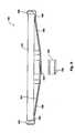
- probe card 30configured in accordance with an embodiment of the present invention is shown in a schematic view.
- probe card 30acts as an interface to an IC testing computer which produces appropriate test signals and senses the response of the ICs under test.
- the probe card 30includes a substrate 32 , typically a PCB substrate, preferably formed of a rigid or semi-rigid material adapted to withstand the stresses associated with IC testing.
- Materials preferred for use in fabricating substrate 32include FR-4 and other glass-filled and ceramic resins, silicon (including monocrystalline silicon, silicon-on-glass, silicon-on-sapphire), germanium, gallium arsenide, or other materials that are well-known in the art.
- substrate 32may be formed so as to have a coefficient of thermal expansion matching, or closely matching, the ICs to be tested.
- Substrate 32is configured with a plurality of conductive traces 34 formed on or adjacent to one or more surfaces thereof. As can be seen in FIG. 1 , the conductive traces 34 extend inwardly from a plurality of test contacts 36 towards a plurality of probe elements 38 .
- an electrically insulating layersuch as silicon dioxide
- the silicon dioxide layercan be formed by methods well-known in the art of silicon-based manufacturing including, for example, chemical vapor deposition (CVD) or exposing a silicon-based substrate to an oxidizing atmosphere for a short time.
- conductive traces 34may also be formed as a metallization layer under one or more surface layers of substrate 32 .
- probe card 30may be constructed in multilayered fashion, with conductive traces 34 located in intermediate layers of substrate 32 .
- the conductive traces 34are formed on a top surface 35 and/or bottom surface 37 of a probe card 30 .
- probe card 30will include one conductive trace 34 in electrical communication with each probe element 38 , although more than one conductive trace 34 per probe element 38 is contemplated within the scope of the present invention.
- a single conductive trace 34may provide electrical signals for more than one probe element 38 during testing.
- in electrical communication withit is meant that the subject electrical components are configured and positioned so as to complete an electrical circuit between one another when the components are supplied with power.
- components in electrical communication with one anotherwill carry an electrical current originating from the same source when the probe card 30 is operational.
- test contacts 36are preferably disposed on a periphery of substrate 32 for electrical interconnection with external testing equipment (not shown).
- the illustrated arrangement of test contacts 36is not intended to be limiting of the present invention, and test contacts 36 may alternatively be disposed on one or both sides of substrate 32 and/or in a range of various locations, including locations in the area of a centermost portion of substrate 32 .
- Conductive traces 34which are in electrical communication with test contacts 36 , thus provide electrical paths for test circuitry to probe elements 38 .
- Conductive traces 34are preferably formed of a highly conductive, low resistivity metal, such as aluminum, copper, titanium, tantalum, molybdenum, or alloys of any thereof.
- Conductive traces 34may be fabricated according to conventional methods well known in the art, including, but not limited to, plating, thin film deposition processes (e.g., CVD, sputtering, photolithography processes and etching), and thick film processes (e.g., stenciling or screen printing).
- platingthin film deposition processes (e.g., CVD, sputtering, photolithography processes and etching)
- thick film processese.g., stenciling or screen printing.
- conductive traces 34may include nonmetallic conductive traces which may be formed of materials such as doped polysilicon.
- an LPCVD processmay be used to form a conductive trace 34 of phosphorous-doped polysilicon.
- probe elements 38are illustrated as a plurality of probe needles.
- the illustration, however,is not intended to be limiting of the present invention, and one of skill in the art will recognize the illustrated probe needles and probe card 30 configuration may be readily substituted for bumps, or other types of electrical contacts known in the art, which are configured for making temporary electrical connections with contact pads of ICs during IC testing.
- Probe elements 38 of probe card 30are arranged in patterns corresponding to patterns of pads on ICs to be tested. For ease of illustration and simplicity in describing the embodiment, only a single pattern of probe elements 38 for testing a single IC is shown. In practice, however, probe card 30 will preferably be configured with a plurality of patterns of probe elements 38 , with each pattern forming a corresponding plurality of test sites for testing a plurality of respective ICs. As such, probe elements 38 may be formed in varying arrays and densities corresponding to the pads of the IC devices to be tested. Each probe element 38 interfaces with a surface portion of substrate 32 adjacent a conductive trace 34 at a probe element-substrate interfacing portion 33 of probe card 30 .
- Probe elements 38are shown mounted on a ring 40 , preferably comprising epoxy, and extending inwardly from a center cutout portion of substrate 32 . This illustrated arrangement, however, is not intended to be limiting of the present invention. Thus, probe elements 38 may be configured on probe card 30 in a multitude of conventional or unconventional configurations. Probe elements 38 may be formed of a variety of conductive materials, including, but not limited to, copper and tungsten. As is readily apparent to one of skill in the art, the diameter, taper, and material of the probe elements 38 , when formed as probe needles, may be varied to determine the spring rate of the probe.
- a fuse 42is interposed in, or located adjacent to, each conductive trace 34 .
- fuses 42are interposed in, or located adjacent to, conductive traces 34 in regions of probe card 30 which are directly adjacent to one of test contacts 36 and probe elements 38 .
- One of skill in the artwill recognize numerous specific locations for fuses 42 , including placement immediately adjacent to, and in electrical communication with, terminating ends of conductive traces 34 (e.g., at interfaces with test contacts 36 and probe elements 38 ).
- fuses 42are further preferably disposed immediately adjacent at least one of a first surface and a second surface of substrate 32 (e.g., a top surface 35 and a bottom surface 37 of substrate 32 ).
- a fuse 42is located such that at least a portion of the fuse 42 is in contact with (either over or under) a surface of substrate 32 , or that a fuse 42 is in close proximity to a surface of substrate 32 .
- a fuse 42 that is in “close proximity” to a surface of substrate 32may, for example, be surrounded by a fuse-holding body (not shown) that is in contact with a surface of substrate 32 .
- fuses 42are interposed adjacently between conductive traces 34 and test contacts 36 and disposed immediately adjacent at least one of a first surface or a second surface of substrate 32 in the case where the conductive traces 34 are carrying signals and/or burn-in voltage into corresponding bond pads of a semiconductor device.
- fuses 42 carrying signals or burn-in voltage away from corresponding bond pads of a semiconductor deviceare disposed immediately adjacent at least one of a first surface or a second surface of substrate 32 and between probe element-substrate interfacing portions 33 of probe card 30 and conductive traces 34 .
- fuses 42are configured to be self-resetting and/or easily repairable or replaceable, such that the probe card 30 may be readily reused for testing at a later time after one or more fuses 42 have been tripped.
- fuses 42are configured to trip (i.e., provide an “open” in the conductive trace circuitry) at a current level below an absolute maximum current that the probe card 30 or the IC device under test can handle without being damaged.
- the current-carrying capacity for a fuse 42may vary depending upon the particular test configuration involving probe card 30 .
- the current-carrying capacity for fuse 42typically will also vary in accordance with various individual components (e.g., resistors, transistors, capacitors, probe elements 38 , etc.) on probe card 30 and/or the particular IC device under test.
- Fuses 42 for use in the present inventionmay be generally classified as active and/or passive fuses.
- a “passive” fuseis a relatively thin conductor which may have its conductive properties disabled upon the application of a predetermined threshold of energy into it.
- the conductive properties of passive fusesmay thus be disabled by passing a current of a higher-than-desired threshold through the fuse, thus causing resistive heating within the fuse that results in the fuse conductor melting, cracking, vaporizing, and/or becoming otherwise nonconductive.
- passive fuses for use in the present inventioninclude materials such as titanium tungsten and platinum silicide.
- Other materials for passive fuses, such as aluminum, copper, nichrome, doped polysilicon, metal silicide or various other conductive metal or alloys,are well known in the art of semiconductor device manufacturing and are also included in the scope of the present invention.
- the passive fusesare formed of the same conductive material(s) as the conductive traces 34 and/or test contacts 36 described herein. Using deposition processes well known in the art, each of fuses 42 may be formed at the same time (simultaneously) as the other fuses 42 . In a related aspect of the embodiment, the passive fuses may thus be constructed at the same time as the conductive traces 34 and/or the test contacts 36 using the same deposition and/or other processing steps (e.g., CVD followed by photopatterning). These passive fuses are typically formed and/or repaired by patterning a deposited layer of the conductive material of the fuse over an insulating dielectric layer, typically silicon dioxide, of substrate 32 .
- an insulating dielectric layertypically silicon dioxide
- the passive fusesmay be prefabricated and placed in electrical communication with testing circuitry on at least one surface of a probe card 30 by mechanical means.
- a passive fuse for use in the present inventionmay comprise two ends of a conductive trace 34 joined by a “neck” having a width considerably smaller than the width of the conductive trace 34 .
- FIG. 2a preferred configuration of a passive fuse 42 a of the present invention is illustrated with passive fuse 42 a interposed in a conductive trace 34 .
- a dielectric layer 45is shown disposed under conductive trace 34 and passive fuse 42 a.
- Passive fuse 42 aincludes trace interfacing portions 44 , 46 in an aspect of the embodiment where the passive fuse 42 a is formed of a material differing from that of conductive trace 34 .
- Passive fuse 42 afurther includes a relatively thin (in comparison to conductive trace 34 and/or trace interfacing portions 44 , 46 ) “neck” or wire portion 48 configured to conduct current up to a predetermined current threshold.
- Trace interfacing portions 44 , 46are in electrical communication with trace end portions 50 , 52 of conductive trace 34 , the trace end portions 50 , 52 otherwise being “open” in relation to one another (i.e., not in electrical communication with each other).
- passive fuse 42 amay simply comprise a neck portion 48 .
- the predetermined current threshold of passive fuse 42 acorresponds to a current level nominally below an absolute maximum current that the probe card 30 or the IC device under test can handle without being damaged. Upon reaching the predetermined current level, passive fuse 42 a trips, disabling the circuit to which passive fuse 42 a is electrically connected.
- Passive fuses 42 amay be formed and/or repaired by conventional methods well known in the art, such as conductive layer deposition techniques, photopatterning processes, and etching techniques. As previously discussed, passive fuses 42 a may be formed concurrently with the deposition of other conductive structures on probe card 30 (e.g., conductive traces 34 , test contacts 36 , bond pads for probe elements, etc.), or passive fuses 42 a may be deposited or placed on probe card 30 in a separate processing step.
- the neck portion 48 of a passive fuse 42 amay be configured of varying widths dependent upon the nature of the application for which it will be used and the materials used in its construction.
- a passive fuse 42 ais configured with a neck portion 48 formed of a material selected from the group consisting of titanium tungsten, aluminum, copper, nichrome, doped polysilicon, platinum silicide, and alloys or combinations of any thereof. Further preferably, the neck portion 48 is configured of a width ranging from about 0.3 micron to about 10.0 microns.
- a second preferred passive fuse configurationis shown in drawing FIG. 3 .
- a passive fuse 42 bis configured, in part, as a cutout of a bond pad 54 , wherein the bond pad 54 may be a test contact 36 or a bonding interface for a conductive trace 34 and a probe element (not shown).
- passive fuse 42 bforms a conductive fuse-type link between bond pad 54 and a conductive trace 34 and is thus also referred to herein as a “linking fuse” 42 b.
- linking fuse 42 bis relatively narrower in width than conductive trace 34 such that linking fuse 42 b will trip in the manner previously described upon the application of an overcurrent into it.
- Linking fuse 42 bmay be fabricated using a variety of techniques which typically involve deposition and photopatterning as previously described.
- a dielectric layer 45is disposed under conductive trace 34 and passive fuse 42 b.
- FIG. 4AA third preferred embodiment of a passive fuse configuration for use in the present invention is shown in section in drawing FIG. 4A .
- a passive fuse 42 cis shown as comprising a dual in-line pin header mounted in through-hole portions 56 of substrate 32 .
- Passive fuse 42 cis configured with pin portions 60 , 62 which are made of conductive material.
- An insulated and removable connector shell 64 containing a fuse conductor 66may be positioned on pin portions 60 , 62 to carry current up to a predetermined threshold from pin portions 60 , 62 .
- through-hole portions 56 of substrate 32are positioned so as to provide an “open” in conductive trace 34 .
- Through-hole portions 56are configured with inner contacts 58 which are in electrical communication with conductive traces 34 .
- pin portions 60 , 62 of the dual in-line pin header passive fuse 42 care placed in through-hole portions 56 of substrate 32 , pin portions 60 , 62 are configured to be in electrical communication with inner contacts 58 , thus completing a current-carrying circuit through conductive trace 34 .
- a passive fuse 42 dconfigured as a dual-in-line socket is shown in drawing FIG. 4B .
- Passive fuse 42 dcomprises pin portions 68 , 70 with an insulated connector shell 72 at one end thereof.
- Pin portions 68 , 70are formed of a conductive material and are in electrical communication with a fuse conductor 74 residing within connector shell 72 .
- through-hole portions 56 of substrate 32are configured with inner contacts 58 and positioned so as to provide an electrical “open” in conductive trace 34 .
- passive fuse 42 dWhen passive fuse 42 d is pressed into through-hole portions 56 and the electrical circuit is completed wherein current can travel from one end portion of a conductive trace 34 to a first inner contact 58 , to a first pin portion 60 , to fuse conductor 74 , to a second pin portion 60 , to a second inner contact 58 , and through to a second end portion of the conductive trace 34 .
- a current which is sufficiently high to trip passive fuse 42 dwill thus disable the circuit.
- the blown passive fuse 42 dis removed, and a new passive fuse 42 d may simply be pressed into through-hole portions 56 .
- passive fuses 42 c and 42 dWith regard to passive fuses 42 c and 42 d, one of skill in the art will readily ascertain that the pin portions of these fuses are adaptable for use with conductive traces 34 that are in intermediate layers in substrate 32 .
- the pin portions of passive fuses 42 c and 42 dmay, for example, extend downwardly through through-hole portions 56 in substrate 32 to contact conductive pads in electrical communication with a conductive trace 34 in an intermediate layer, thus completing a circuit through the trace.
- passive fuses 42 c and 42 dare but two examples of discrete electrical components that may be used as protective fuses for purposes of the present invention. It will be readily apparent to one skilled in the art that various other conventional designs for discrete electrical components may be readily utilized herein. By use of the term “discrete electrical component,” it is meant that the particular electrical component is manufactured separately from the probe card 30 and thus subsequently attached thereto or otherwise integrated therein.
- each of passive fuses 42 a, 42 b, 42 c and 42 dis configured to conduct current under a threshold which will cause damage to probe card 30 and to become disabled when a test current exceeds a threshold under the probe card's maximum current-carrying capacity.
- a higher than desired current in a conductive trace 34(and/or in other components in which a passive fuse 42 a, 42 b, 42 c or 42 d is placed) will cause the passive fuse 42 a, 42 b, 42 c or 42 d to trip by resistive heating within the fuse, the resistive heating resulting in the fuse conductor (i.e., neck portion 48 ) melting, cracking, vaporizing or the like.
- passive fuses 42 a, 42 b, 42 c and 42 dmay be replaced or repaired such that probe card 30 may be reused at a later time.
- “Active” fusesmay also be used to protect probe cards and the components thereon in accordance with the principles of the present invention.
- “Active fuses,” as used herein,are electronic circuits configured to conduct current up to a predetermined level wherein once the predetermined level of current has been exceeded, active fuses are configured to stop conducting current, thus disabling the circuit to which the active fuses are connected. Unlike passive fuses, however, active fuses are configured to automatically reset upon removal of the current overload. Upon self-resetting, the active fuses are again operational to carry current to and from the probe elements on the probe card.
- the active fuses for use in the present inventionare fast tripping surface mount-type fuses.
- a bimetallic switchmay be used as an active fuse according to the present invention.
- the bimetallic switch as an active fusemay be interposed in, or located adjacent to, a conductive trace 34 in order to limit undesirably high current levels potentially traveling through a probe card 30 .
- a simplified bimetallic switch 76is shown in FIGS. 5A and 5B in electrical communication with portions of a conductive trace 34 over a dielectric layer 45 of a probe card 30 .
- bimetallic switch 76is formed of a first metal conductor 78 and a second metal conductor 80 having differing rates of thermal expansion.
- first metal conductor 78 and a second metal conductor 80are configured to be in contact with one another for conducting current up to a predetermined current threshold.
- the currentbecomes excessive (e.g., potentially damaging to the probe card 30 and/or an IC device under test)
- the temperature of first metal conductor 78 and second metal conductor 80rises, causing first metal conductor 78 (having a relatively higher rate of thermal expansion) to bend away from second metal conductor 80 .
- first metal conductor 78 and second metal conductor 80bend away from each other, the contact between first metal conductor 78 and second metal conductor 80 eventually opens, thus interrupting current flow in conductive trace 34 ( FIG. 5B ).
- the disruption of electrical current to conductive trace 34 resulting from the “open contact”causes the temperature of first metal conductor 78 and second metal conductor 80 to fall, thus allowing the contacts to reclose and permitting the current to flow again.
- FIGS. 6A, 6B , 6 C and 6 DA series of embodiments of an active fuse on a probe card are shown in drawing FIGS. 6A, 6B , 6 C and 6 D.
- the active fusecomprises a Polymer Positive Temperature Coefficient (PPTC) fuse as an overcurrent protection mechanism interposed in, or located adjacent to, a conductive trace 34 on a probe card 30 .
- PPTCPolymer Positive Temperature Coefficient
- FIGS. 6A, 6C and 6 DVarious lead arrangements for PPTC fuses are shown in FIGS. 6A, 6C and 6 D.
- a PPTC active fuse 82 ais shown having a radial lead arrangement positioned in a through-hole portion 56 of substrate 32 and in electrical communication with inner contacts 58 .
- FIG. 6Bthe PPTC active fuse 82 a of FIG. 6A is shown in tripped condition.
- a PPTC active fuse 82 b having an axial lead arrangement with terminals 84 , 86 in electrical communication with conductive trace 34is shown in FIG. 6C .
- a PPTC active fuse 82 c in a surface mount configuration known in the artis shown in FIG. 6D . Fuses 82 b and 82 c may be electrically connected to conductive traces 34 in a manner well known in the art, to include the use of conventional soldering techniques.
- the PPTC active fuses 82 a, 82 b and 82 c for use in the present inventionare constructed with highly conductive carbon particles 88 combined with a nonconductive polymer 90 that exhibits two phases.
- a first phasewhich occurs under a predetermined current threshold, the polymer 90 exhibits a crystalline or semi-crystalline structure in which the molecules form long chains and are arranged in a regular structure ( FIG. 6A ).
- the carbon particles 88are packed within the crystalline polymer structure, thus forming a conductive chain spanning between opposing electrodes of the PPTC fuse 82 a.
- the polymer 90After the circuit has been opened for a certain period of time, the polymer 90 cools and returns to its normal crystalline state, thus allowing the carbon particles 88 to again touch and form conductive paths, upon which the circuit closes and the probe card can function properly.
- the PPTC fusesare advantageously self-resetting and do not have to be replaced as is the case with conventional passive fuses.
- the PPTC fuses for use in the present inventionwill have trip times of just a few milliseconds.
- Such PPTC fusesare presently available from several commercial sources, including Raychem Corporation (Menlo Park, Calif.) and Bourns Incorporated (Ogden, Utah).
- the present inventioncontemplates a plurality of fuses interposed in, or located adjacent to, a plurality of respective conductive traces.
- the fusesmay be passive fuses, active fuses, or combinations thereof.
- the use of an active fusemay be particularly desirable in the situation where a particular location of the fuse on the probe card renders the fuse not easily repairable or replaceable.
- Passive fusesmay be particularly desirable in the situation where extremely short trip times are desirable and/or the location of the fuse renders it readily repairable or replaceable.
- passive fusesmay be preferable for placement in probe card conductive traces used for supplying relatively high voltages during IC testing (e.g., voltages supplied for burn-in testing of ICs).
- At least one fuse according to the present inventionis interposed in, or located adjacent to, each conductive trace.
- some, but not all, of the conductive tracesmay include a fuse configured according to the present invention.
- a fusemay not be needed in one or more conductive traces on a probe card where the one or more conductive traces will be transporting extremely low voltage signals to an IC device under test.
- the test system 100typically includes a wafer handler (not shown) for handling and positioning a semiconductor wafer 112 , test equipment 114 for generating test signals, and a probe card 116 for making temporary electrical connections with the semiconductor wafer 112 .
- Semiconductor wafer 112is configured with a plurality of bond pads 113 on an active surface thereof representing a plurality of unsingulated ICs 118 .
- Probe card 116is configured with a plurality of conductive traces 120 over at least one surface thereof. Interposed in, and/or located adjacent to, at least some, and preferably all, of the conductive traces 120 are fuses 122 provided in accordance with the above-described principles of the present invention.
- a prober 124typically lowers the probe card 116 on the semiconductor wafer 112 until probe elements 126 of probe card 116 come in contact with bond pads 113 on semiconductor wafer 112 .
- Probe elements 126are shown as needles, but may alternatively be configured as bumps, or other types of electrical contacts known in the art for making temporary electrical connections with bond pads 113 of semiconductor wafer 112 .
- Test equipment 114is in electrical communication with the test contacts 117 on probe card 116 and, upon activation, transmits test signals through the test contacts 117 and conductive traces 120 to probe elements 126 .
- the semiconductor wafer 112may be raised into contact with the probe elements 126 of probe card 116 of a prober 124 .
- the semiconductor wafer 112 or the probe card 116is stepped so that unsingulated dice on the semiconductor wafer 112 are tested in groups of two or more at a time in sequence.
- the test system 100may also be configured to test all unsingulated dice on semiconductor wafer 112 at the same time.
- test equipment 114Upon probe elements 126 coming in contact with bond pads 113 of semiconductor wafer 112 , test equipment 114 applies test signals and/or a power source voltage through probe card 116 to bond pads 113 and analyzes the resulting signals therefrom.
- fuses 122protect probe card 116 and/or the ICs 118 on semiconductor wafer 112 from overcurrents and/or short circuits in the ICs 118 .
- one or more fuses 122 exposed to the current overloadwill trip, thus disabling the circuit extending through probe card 116 . If the one or more of the tripped fuses are configured as “active” fuses, the fuses will automatically reset after the fuse cools, thus rendering probe card 116 operational again. If the one or more tripped fuses are configured as “passive” fuses, the probe card 116 may be reused after the tripped fuses are repaired or replaced (depending upon the particular type of passive fuse used).
- test system 100is only exemplary, and the test apparatus may be configured for any of a variety of device tests on semiconductor wafer 112 .
- Such testingmay, for example, include basic parametric tests, low frequency functional testing, speed binning tests using specially designed test structures, boundary scan testing, and device testing at full operating frequency.
- a plurality of protective fuses 138can be configured as, interposed in, or placed adjacent to, pogo pin 140 portions of a probe card assembly 135 (drawing FIG. 8 ). As shown in drawing FIG. 8 , pogo pins 140 form an interface between testing circuitry (not shown) and test contacts 142 on a probe card 136 .
- pogo pins 140may be formed, in part, as a fuse body for holding one or more protective fuses 138 .
- protective fuses 138are illustrated as forming a portion of pogo pins 140 .
- Pogo pins 140enable a probe card 136 to be electrically connected with test equipment (not shown).
- pogo pins 140including protective fuses 138 , are electrically connected to conductive traces 144 on probe card 136 via test contacts 142 residing on a probe card surface.
- Test signalsare transmitted from the test equipment to probe card 136 by way of pogo pins 140 and protective fuses 138 .
- Protective fuses 138are configured to prevent excessive currents from being transmitted to probe card 136 , thus preventing damage to probe card 136 .
- Protective fuses 138further prevent excessive currents from traveling through probe needles 146 to one or more IC devices 148 under test.
- protective fuses 138 which have been tripped due to excessive currentmay be replaced by, for example, inserting a new protective fuse 138 into a pogo pin 140 in the aspect of the embodiment where a pogo pin 140 is configured, in part, as a fuse body.
- probe cards for use in the present inventionmay comprise any type of probe card susceptible to the introduction of one or more fuses for the electrical protection of the probe card and/or components thereof.
- probe card configurationsincluding, but not limited to, vertical contact probe cards, cantilever-type probe cards, and probe cards for wafer level burn-in.
- fuses described hereinare suitable for use with a variety of other electrical components which may be found on a probe card. These components include resistors, transistors, capacitors, diodes, and the like.
- Membrane-type probe card 150includes a carrier substrate 151 supporting a membrane 154 and a plurality of contact bumps 152 connected through the membrane 154 to conductive traces 156 .
- Conductive traces 156are in electrical communication with test contacts 158 .
- Conductive traces 156thus carry test signals from multichannel testing equipment (not shown) to contact bumps 152 .
- contact bumps 152supply test signals from the testing equipment to contact pads 162 on an IC device under test 164 .
- Interposed in, or adjacent to, conductive traces 156are fuses 160 configured in accordance with the principles of the present invention.
Landscapes
- Physics & Mathematics (AREA)
- General Physics & Mathematics (AREA)
- Engineering & Computer Science (AREA)
- Microelectronics & Electronic Packaging (AREA)
- Computer Hardware Design (AREA)
- General Engineering & Computer Science (AREA)
- Testing Or Measuring Of Semiconductors Or The Like (AREA)
- Measuring Leads Or Probes (AREA)
Abstract
Description
- This application is a continuation of application Ser. No. 09/888,689, filed Jun. 25, 2001, pending.
- Field of the Invention: The present invention relates generally to probe cards for testing the electric characteristics of semiconductor dice. More specifically, the present invention relates to probe cards configured with protective circuitry suitable for use in electrical testing of semiconductor dice without damage to the probe cards.
- In the manufacture of semiconductor devices, a large number of semiconductor devices, also known as dice or integrated circuit chips (ICs or chips), are formed on a semiconductor wafer by using, for example, precision photolithographic technologies. These fabricated semiconductor devices are subjected to a series of test procedures in order to assess the electrical characteristics of the integrated circuits contained on the semiconductor devices. Semiconductor devices which have been found to be satisfactory by testing procedures are selectively transferred for subsequent processing such as die attach, wire bonding, and encapsulation. New integrated circuit designs and higher unit volumes are additional considerations that drive testing of ICs. Also, as IC devices become more complex, the need for high-speed and accurate testing becomes increasingly important.
- IC device testing procedures conventionally include “wafer-level probe testing” in which individual ICs or groups of ICs, while still on the wafer, are initially tested to determine functionality and/or speed. Wafer probing establishes a temporary electrical contact between the IC and the automatic test equipment and is a critical step for verifying design and performance of the IC and for sorting ICs before singulation and costly packaging. Other tests, such as speed testing and “burn-in” testing, are typically performed after the dice have been singulated from the wafer. IC testing further typically involves testing for various performance parameters while changing environmental conditions such as temperature, voltage and current.
- Typically, testing at the wafer level involves the use of probe cards and other test heads to electrically test ICs by making electrical connection interfaces with groups of ICs or a single IC at a time. If the wafer has a yield of ICs which indicates that the quality and quantity of functional ICs is likely to be good, the individual ICs are singulated or “diced” from the wafer with a wafer saw. Each individual die may be assembled in a package to form an IC device, or may be bumped with solder (usually prior to separation from the wafer) for direct flip-chip bonding to a semiconductor substrate. Other various packaging means may also be used, as is known to those of skill in the art.
- The test signals can include specific combinations of voltages and/or currents transmitted through the probe card to the ICs on the wafer. During the test procedure, response signals such as voltage, current and frequency are analyzed and compared to required values by a test controller. Thus, by applying the appropriate voltages and/or currents and monitoring the device response, a computer program running the testing apparatus determines the functionality of the die. The integrated circuits that do not meet specification can be marked or mapped in software. Following testing, defective circuits in the ICs may be repaired by actuating fuses (or anti-fuses) to inactivate the defective circuitry and substitute redundant circuitry.
- Conventional probe cards can be generally classified into two categories: needle-type probe cards and membrane-type probe cards. Needle-type probe cards are the most common type of probe card and include elongated probe needles mounted on an annular ring. A typical probe needle is a pointed needle-like element of small size, with a tip that tapers down into a sharp point. When mounted on the annular ring, the probe needles typically have their free ends pointing downward and are carefully aligned with the ends of all the other probe needles to be in a single plane. An exemplary probe needle configuration is disclosed in U.S. Pat. No. 5,532,613 to Nagasawa et al., which includes a probe needle having a pointed or conical tip. Probe needles are typically made of tungsten, but materials such as beryllium copper, palladium, and rhenium tungsten are also used.
- The probe needles are typically secured to the annular ring by epoxy or are bonded, as by welding, to a blade and are adapted to make temporary electrical connections between contact locations on the dice (e.g., bond pads, fuse pads, test pads) and external test circuitry. The annular ring, in turn, is attached to a printed circuit board (PCB) substrate. The PCB substrate typically includes electrical traces in electrical communication with the probe needles. An exemplary probe card having probe needles is described in U.S. Pat. 4,757,256 to Whann et al.
- Membrane-type probe cards are typically formed as having tungsten contact bumps disposed on a thin, flexible dielectric material, such as polyimide, as the membrane. Membrane-type probe cards commonly employ a multilayer, flexible PCB interconnection structure configured with fine pitch traces leading to low inductance bump array structures aligned with the location of the pads of the device under test (e.g., a semiconductor die being tested). In a conventional membrane probing system, contact bumps of the bump array structures are pressed down via an elastic body interposed between the contact bumps and the membrane, such that any height variation among the contact bumps can be absorbed by the flexible thickness of the elastic body. Exemplary membrane-type probe cards are disclosed in U.S. Pat. No. 4,906,920 to Huff et al. and in U.S. Pat. No. 6,181,145 to Tomita et al.
- Needle-type probe cards and membrane-type probe cards may be further configured to meet the needs of the particular devices under test. In this regard, the probe cards may be specially configured as vertical contact probe cards (used, for example, to test LOGIC devices of a C4 type), cantilever-type probe cards (generally used to test inner-leads of LCD drivers with super fine-pitch (e.g., 40 micron-pitch) bumps), probe cards for wafer level burn-in, probe cards configured to test high-speed microprocessor units (MPUs) with high pin counts, as well as various other types of probe cards known in the art.
- In all types of probe cards, the testing voltage current is carried from an external test circuit to the pad connecting sections (probe elements) of the probe cards through conductive traces or wiring in electrical communication therewith.
- One concern in the art is over the application of excessive voltage to the IC chip under test. In this regard, U.S. Pat. No. 6,127,837 to Yamamoto et al. (“Yamamoto”) describes a series of resistance, transistor and capacitance structures formed on a probe wafer between a test bump and a shared power/signal line. According to Yamamoto, the resistance, transistor and capacitance structures prevent overshoot or undershoot of signals supplied to the bump and also prevent the application of excessive voltage or current to the chip. Yamamoto, however, does not disclose methods or apparatus for protection of the probe wafer and further does not describe a probe card configured to carry the current-regulating structures.
- The delivery of excessive voltage during probe testing to an IC may also result in damage to the probe card. In Japanese Patent Application 61174771, a small fuse is provided on the back side surface of a probe card in order to prevent the end of a probe needle connected to a grounding pad from seizing due to an overcurrent delivered to a short-circuited IC. Japanese Patent Application 0115367 discloses a thermal fuse fixed between a probe needle and power source which generates heat and becomes fused before a probe pin generates heat and is fused. Each of these patent applications, however, is drawn to means for preventing seizing and fusing of a probe needle routed to ground and power and does not address the limitation of current through the probe card in general or through any probe needle which might otherwise cause that probe needle to become nonfunctional.
- Japanese Patent Application 04265541 discloses an array of easily exchanged fuses interposed between corresponding probes on a probe card and a power supply. The apparatus disclosed therein, however, is relatively bulky in that the fuses are vertically disposed over the probe card and the apparatus includes a fuse body for holding the fuses.
- Accordingly, what is needed in the art is a probe card configuration designed to limit current to a plurality of varying probe elements, not just ground and power. It would also be advantageous to provide a probe card with one or more fuses that are self-resetting, or readily replaceable and/or repairable. Fuses which can be fabricated simultaneously with other components on the probe card using processes which are well known in the semiconductor arts are also desirable. A probe card thus manufactured would extend the life of the probe card, therefore, saving time, materials, and costs for those involved in semiconductor dice testing operations.
- In accordance with one aspect of the invention, a method of forming a probe card is provided. The method comprises providing a substrate having a first surface and a second surface; disposing a plurality of conductive traces adjacent at least one of the first surface and the second surface; providing a plurality of probe elements in electrical communication with the plurality of conductive traces; and providing a plurality of fuse elements in respective electrical communication with at least some of the plurality of conductive traces, at least some of the plurality of fuse elements disposed immediately adjacent at least one of the first surface and the second surface. Additionally, the fuse elements may be passive or active fuse elements, and the fuse elements may further be configured to be self-resetting, repairable and/or replaceable. In a preferred embodiment, substantially all of the conductive traces are provided with a respective fuse element.
- A method of fabricating a probe card is also provided. The method comprises providing a probe card substrate; providing a plurality of conductive traces over a surface of the probe card substrate; providing a plurality of probe elements in electrical communication with the plurality of conductive traces wherein at least one of the probe elements is configured for supplying a test signal to at least one semiconductor die and wherein a second probe element is configured for receiving a test signal from the at least one semiconductor die; and providing at least one repairable or replaceable component in electrical communication with at least some of the plurality of conductive traces.
- In a still further embodiment, a method of using a probe card for testing at least one semiconductor die is disclosed. The method comprises providing a probe card having a plurality of probe elements connected thereto, the probe elements configured for supplying test signals to the at least one semiconductor die; providing a fuse in electrical communication with at least some of the probe elements; and testing the at least one semiconductor die by supplying test signals.
- In accordance with another aspect of the invention, a probe card is provided. The probe card includes a substrate having a first surface and a second surface; a plurality of conductive traces disposed adjacent at least one of the first surface and the second surface; a plurality of probe elements in respective electrical communication with the conductive traces; and a plurality of fuses in respective electrical communication with the conductive traces.
- In yet another embodiment of the invention, a semiconductor die testing system is disclosed. The semiconductor die testing system comprises a probe card including a substrate having a first surface and a second surface; a plurality of conductive traces disposed adjacent at least one of the first surface and the second surface; a plurality of probe elements in electrical communication with the conductive traces; a plurality of fuses in electrical communication with the conductive traces; and semiconductor device testing apparatus linkable with the probe card, the semiconductor device testing apparatus configured for sending test signals through the probe card.
- The foregoing and other advantages of the invention will become apparent upon reading the following detailed description and upon reference to the drawings in which:
FIG. 1 is a schematic view of a probe card according to an embodiment of the present invention;FIGS. 2 and 3 are perspective views of fuse embodiments of the present invention;FIGS. 4A and 4B are schematic views of fuse embodiments according to the present invention;FIGS. 5A and 5B are simplified perspective views of active fuse embodiments of the present invention;FIGS. 6A-6D are simplified diagrams of other active fuse embodiments of the present invention;FIG. 7 is a simplified diagram of a test system in accordance with the present invention;FIG. 8 illustrates a still further embodiment of the present invention; andFIG. 9 shows a probe card embodiment of the present invention.- As noted throughout the disclosure, the present invention provides various advantages, including the ability to perform a multitude of tests, such as functional, parametric, burn-in, high frequency, and other tests, without risk of damage to the probe card. Performing IC testing according to the present invention provides significant cost savings in protecting and allowing reuse of probe cards which might otherwise be damaged by high test temperatures, electrical overloads, and various other sources of electrical failure or operator error during the testing process.
- As used herein, use of the term “IC testing” encompasses both static testing, where the IC is simply powered up, and dynamic testing, where the IC is powered up and is sent signals exercising some degree of functionality over the IC.
- Referring to drawing
FIG. 1 , anexemplary probe card 30 configured in accordance with an embodiment of the present invention is shown in a schematic view. As described in more detail herein,probe card 30 acts as an interface to an IC testing computer which produces appropriate test signals and senses the response of the ICs under test. Theprobe card 30 includes asubstrate 32, typically a PCB substrate, preferably formed of a rigid or semi-rigid material adapted to withstand the stresses associated with IC testing. Materials preferred for use in fabricatingsubstrate 32 include FR-4 and other glass-filled and ceramic resins, silicon (including monocrystalline silicon, silicon-on-glass, silicon-on-sapphire), germanium, gallium arsenide, or other materials that are well-known in the art. In one aspect of the embodiment,substrate 32 may be formed so as to have a coefficient of thermal expansion matching, or closely matching, the ICs to be tested. Substrate 32 is configured with a plurality ofconductive traces 34 formed on or adjacent to one or more surfaces thereof. As can be seen inFIG. 1 , the conductive traces34 extend inwardly from a plurality oftest contacts 36 towards a plurality ofprobe elements 38. Whensubstrate 32 is made of a semiconductor material, an electrically insulating layer, such as silicon dioxide, can be formed onsubstrate 32 to provide an insulative surface forconductive traces 34 andtest contacts 36. The silicon dioxide layer can be formed by methods well-known in the art of silicon-based manufacturing including, for example, chemical vapor deposition (CVD) or exposing a silicon-based substrate to an oxidizing atmosphere for a short time.- In accordance with recognized practices in the semiconductor art,
conductive traces 34 may also be formed as a metallization layer under one or more surface layers ofsubstrate 32. Thus, in a second aspect of the embodiment,probe card 30 may be constructed in multilayered fashion, withconductive traces 34 located in intermediate layers ofsubstrate 32. In the currently preferred configuration, the conductive traces34 are formed on atop surface 35 and/orbottom surface 37 of aprobe card 30. Typically,probe card 30 will include oneconductive trace 34 in electrical communication with eachprobe element 38, although more than oneconductive trace 34 perprobe element 38 is contemplated within the scope of the present invention. In other configurations (not shown), a singleconductive trace 34 may provide electrical signals for more than oneprobe element 38 during testing. - By use of the term “in electrical communication with,” it is meant that the subject electrical components are configured and positioned so as to complete an electrical circuit between one another when the components are supplied with power. Thus, components in electrical communication with one another will carry an electrical current originating from the same source when the
probe card 30 is operational. - As shown in
FIG. 1 ,test contacts 36 are preferably disposed on a periphery ofsubstrate 32 for electrical interconnection with external testing equipment (not shown). The illustrated arrangement oftest contacts 36, however, is not intended to be limiting of the present invention, andtest contacts 36 may alternatively be disposed on one or both sides ofsubstrate 32 and/or in a range of various locations, including locations in the area of a centermost portion ofsubstrate 32. Conductive traces34, which are in electrical communication withtest contacts 36, thus provide electrical paths for test circuitry to probeelements 38. Conductive traces34 are preferably formed of a highly conductive, low resistivity metal, such as aluminum, copper, titanium, tantalum, molybdenum, or alloys of any thereof. Conductive traces34 may be fabricated according to conventional methods well known in the art, including, but not limited to, plating, thin film deposition processes (e.g., CVD, sputtering, photolithography processes and etching), and thick film processes (e.g., stenciling or screen printing). - Various other types of conductive traces known in the art are also contemplated for use in the present invention. As a nonlimiting example, conductive traces34 may include nonmetallic conductive traces which may be formed of materials such as doped polysilicon. In this aspect of the embodiment, an LPCVD process may be used to form a
conductive trace 34 of phosphorous-doped polysilicon. - Still referring to
FIG. 1 ,probe elements 38 are illustrated as a plurality of probe needles. The illustration, however, is not intended to be limiting of the present invention, and one of skill in the art will recognize the illustrated probe needles andprobe card 30 configuration may be readily substituted for bumps, or other types of electrical contacts known in the art, which are configured for making temporary electrical connections with contact pads of ICs during IC testing. - Probe
elements 38 ofprobe card 30 are arranged in patterns corresponding to patterns of pads on ICs to be tested. For ease of illustration and simplicity in describing the embodiment, only a single pattern ofprobe elements 38 for testing a single IC is shown. In practice, however,probe card 30 will preferably be configured with a plurality of patterns ofprobe elements 38, with each pattern forming a corresponding plurality of test sites for testing a plurality of respective ICs. As such,probe elements 38 may be formed in varying arrays and densities corresponding to the pads of the IC devices to be tested. Eachprobe element 38 interfaces with a surface portion ofsubstrate 32 adjacent aconductive trace 34 at a probe element-substrate interfacing portion 33 ofprobe card 30. - Probe
elements 38 are shown mounted on aring 40, preferably comprising epoxy, and extending inwardly from a center cutout portion ofsubstrate 32. This illustrated arrangement, however, is not intended to be limiting of the present invention. Thus, probeelements 38 may be configured onprobe card 30 in a multitude of conventional or unconventional configurations. Probeelements 38 may be formed of a variety of conductive materials, including, but not limited to, copper and tungsten. As is readily apparent to one of skill in the art, the diameter, taper, and material of theprobe elements 38, when formed as probe needles, may be varied to determine the spring rate of the probe. - With further reference to drawing
FIG. 1 , afuse 42 is interposed in, or located adjacent to, eachconductive trace 34. Preferably, fuses42 are interposed in, or located adjacent to, conductive traces34 in regions ofprobe card 30 which are directly adjacent to one oftest contacts 36 and probeelements 38. One of skill in the art will recognize numerous specific locations forfuses 42, including placement immediately adjacent to, and in electrical communication with, terminating ends of conductive traces34 (e.g., at interfaces withtest contacts 36 and probe elements38). - In a related aspect of the embodiment, fuses42 are further preferably disposed immediately adjacent at least one of a first surface and a second surface of substrate32 (e.g., a
top surface 35 and abottom surface 37 of substrate32). By use of the phrase “disposed immediately adjacent” at least one of a first surface and a second surface ofsubstrate 32, it is meant that afuse 42 is located such that at least a portion of thefuse 42 is in contact with (either over or under) a surface ofsubstrate 32, or that afuse 42 is in close proximity to a surface ofsubstrate 32. Afuse 42 that is in “close proximity” to a surface ofsubstrate 32 may, for example, be surrounded by a fuse-holding body (not shown) that is in contact with a surface ofsubstrate 32. - In a preferred embodiment, fuses42 are interposed adjacently between
conductive traces 34 andtest contacts 36 and disposed immediately adjacent at least one of a first surface or a second surface ofsubstrate 32 in the case where the conductive traces34 are carrying signals and/or burn-in voltage into corresponding bond pads of a semiconductor device. In a related aspect of a preferred embodiment, fuses42 carrying signals or burn-in voltage away from corresponding bond pads of a semiconductor device are disposed immediately adjacent at least one of a first surface or a second surface ofsubstrate 32 and between probe element-substrate interfacing portions 33 ofprobe card 30 and conductive traces34. - In a most preferred embodiment of the present invention, fuses42 are configured to be self-resetting and/or easily repairable or replaceable, such that the
probe card 30 may be readily reused for testing at a later time after one ormore fuses 42 have been tripped. Preferably, fuses42 are configured to trip (i.e., provide an “open” in the conductive trace circuitry) at a current level below an absolute maximum current that theprobe card 30 or the IC device under test can handle without being damaged. The current-carrying capacity for afuse 42 may vary depending upon the particular test configuration involvingprobe card 30. The current-carrying capacity forfuse 42 typically will also vary in accordance with various individual components (e.g., resistors, transistors, capacitors,probe elements 38, etc.) onprobe card 30 and/or the particular IC device under test. Fuses 42 for use in the present invention may be generally classified as active and/or passive fuses. As used herein, a “passive” fuse is a relatively thin conductor which may have its conductive properties disabled upon the application of a predetermined threshold of energy into it. In the context of the invention, the conductive properties of passive fuses may thus be disabled by passing a current of a higher-than-desired threshold through the fuse, thus causing resistive heating within the fuse that results in the fuse conductor melting, cracking, vaporizing, and/or becoming otherwise nonconductive. Preferably, passive fuses for use in the present invention include materials such as titanium tungsten and platinum silicide. Other materials for passive fuses, such as aluminum, copper, nichrome, doped polysilicon, metal silicide or various other conductive metal or alloys, are well known in the art of semiconductor device manufacturing and are also included in the scope of the present invention.- In one aspect of a preferred embodiment of the invention, the passive fuses are formed of the same conductive material(s) as the conductive traces34 and/or
test contacts 36 described herein. Using deposition processes well known in the art, each offuses 42 may be formed at the same time (simultaneously) as the other fuses42. In a related aspect of the embodiment, the passive fuses may thus be constructed at the same time as the conductive traces34 and/or thetest contacts 36 using the same deposition and/or other processing steps (e.g., CVD followed by photopatterning). These passive fuses are typically formed and/or repaired by patterning a deposited layer of the conductive material of the fuse over an insulating dielectric layer, typically silicon dioxide, ofsubstrate 32. - In other embodiments of passive fuses, the passive fuses may be prefabricated and placed in electrical communication with testing circuitry on at least one surface of a
probe card 30 by mechanical means. - It will be apparent to one of skill in the art that while preferred fuse embodiments are described below, the present invention is not intended to be limited by the described embodiments. In this regard, the present invention incorporates by reference the various embodiments of fuses for use with ICs as disclosed in U.S. Pat. No. 4,198,744 to Nicolay, U.S. Pat. No. 4,682,204 to Shiozaki et al. and U.S. Pat. No. 5,608,257 to Lee et al.
- In its simplest form, a passive fuse for use in the present invention may comprise two ends of a
conductive trace 34 joined by a “neck” having a width considerably smaller than the width of theconductive trace 34. Referring now to drawingFIG. 2 , a preferred configuration of apassive fuse 42aof the present invention is illustrated withpassive fuse 42ainterposed in aconductive trace 34. Adielectric layer 45 is shown disposed underconductive trace 34 andpassive fuse 42a.Passive fuse 42aincludestrace interfacing portions passive fuse 42ais formed of a material differing from that ofconductive trace 34.Passive fuse 42afurther includes a relatively thin (in comparison toconductive trace 34 and/ortrace interfacing portions 44,46) “neck” orwire portion 48 configured to conduct current up to a predetermined current threshold.Trace interfacing portions trace end portions conductive trace 34, thetrace end portions - In an embodiment where the
conductive trace 34 and thepassive fuse 42aare formed of the same materials, it should be understood that separatetrace interfacing portions passive fuse 42aneed not be formed, andpassive fuse 42amay simply comprise aneck portion 48. - Preferably, the predetermined current threshold of
passive fuse 42acorresponds to a current level nominally below an absolute maximum current that theprobe card 30 or the IC device under test can handle without being damaged. Upon reaching the predetermined current level,passive fuse 42atrips, disabling the circuit to whichpassive fuse 42ais electrically connected. - Passive fuses42amay be formed and/or repaired by conventional methods well known in the art, such as conductive layer deposition techniques, photopatterning processes, and etching techniques. As previously discussed,
passive fuses 42amay be formed concurrently with the deposition of other conductive structures on probe card30 (e.g., conductive traces34,test contacts 36, bond pads for probe elements, etc.), orpassive fuses 42amay be deposited or placed onprobe card 30 in a separate processing step. Theneck portion 48 of apassive fuse 42amay be configured of varying widths dependent upon the nature of the application for which it will be used and the materials used in its construction. In a preferred aspect of the invention, apassive fuse 42ais configured with aneck portion 48 formed of a material selected from the group consisting of titanium tungsten, aluminum, copper, nichrome, doped polysilicon, platinum silicide, and alloys or combinations of any thereof. Further preferably, theneck portion 48 is configured of a width ranging from about 0.3 micron to about 10.0 microns. - A second preferred passive fuse configuration is shown in drawing
FIG. 3 . Here, apassive fuse 42bis configured, in part, as a cutout of abond pad 54, wherein thebond pad 54 may be atest contact 36 or a bonding interface for aconductive trace 34 and a probe element (not shown). In this embodiment,passive fuse 42bforms a conductive fuse-type link betweenbond pad 54 and aconductive trace 34 and is thus also referred to herein as a “linking fuse”42b.As can be seen inFIG. 3 , linkingfuse 42bis relatively narrower in width thanconductive trace 34 such that linkingfuse 42bwill trip in the manner previously described upon the application of an overcurrent into it. Linkingfuse 42bmay be fabricated using a variety of techniques which typically involve deposition and photopatterning as previously described. Adielectric layer 45 is disposed underconductive trace 34 andpassive fuse 42b. - A third preferred embodiment of a passive fuse configuration for use in the present invention is shown in section in drawing
FIG. 4A . In this embodiment, a passive fuse42cis shown as comprising a dual in-line pin header mounted in through-hole portions 56 ofsubstrate 32. Passive fuse42cis configured withpin portions removable connector shell 64 containing afuse conductor 66 may be positioned onpin portions pin portions hole portions 56 ofsubstrate 32 are positioned so as to provide an “open” inconductive trace 34. Through-hole portions 56 are configured withinner contacts 58 which are in electrical communication with conductive traces34. Whenpin portions hole portions 56 ofsubstrate 32,pin portions inner contacts 58, thus completing a current-carrying circuit throughconductive trace 34. - As previously discussed, an overload of current sufficient to damage the
probe card 30, components thereof, or an IC device under test will trip thefuse conductor 66, thus disabling the circuit extending through passive fuse42c.Upon blowing passive fuse42c,anew connector shell 64 and/ornew pin portions hole portions 56 ofsubstrate 32 to renderprobe card 30 operational again. - In a related embodiment, a
passive fuse 42dconfigured as a dual-in-line socket is shown in drawingFIG. 4B .Passive fuse 42dcomprisespin portions insulated connector shell 72 at one end thereof.Pin portions fuse conductor 74 residing withinconnector shell 72. Similar to the embodiment shown inFIG. 4A , through-hole portions 56 ofsubstrate 32 are configured withinner contacts 58 and positioned so as to provide an electrical “open” inconductive trace 34. Whenpassive fuse 42dis pressed into through-hole portions 56 and the electrical circuit is completed wherein current can travel from one end portion of aconductive trace 34 to a firstinner contact 58, to afirst pin portion 60, to fuseconductor 74, to asecond pin portion 60, to a secondinner contact 58, and through to a second end portion of theconductive trace 34. A current which is sufficiently high to trippassive fuse 42dwill thus disable the circuit. To restore the circuit, the blownpassive fuse 42dis removed, and a newpassive fuse 42dmay simply be pressed into through-hole portions 56. - With regard to
passive fuses 42cand42d,one of skill in the art will readily ascertain that the pin portions of these fuses are adaptable for use withconductive traces 34 that are in intermediate layers insubstrate 32. In this regard, the pin portions ofpassive fuses 42cand42dmay, for example, extend downwardly through through-hole portions 56 insubstrate 32 to contact conductive pads in electrical communication with aconductive trace 34 in an intermediate layer, thus completing a circuit through the trace. - Furthermore,
passive fuses 42cand42dare but two examples of discrete electrical components that may be used as protective fuses for purposes of the present invention. It will be readily apparent to one skilled in the art that various other conventional designs for discrete electrical components may be readily utilized herein. By use of the term “discrete electrical component,” it is meant that the particular electrical component is manufactured separately from theprobe card 30 and thus subsequently attached thereto or otherwise integrated therein. - With reference to
FIGS. 2, 3 ,4A and4B, each ofpassive fuses card 30 and to become disabled when a test current exceeds a threshold under the probe card's maximum current-carrying capacity. Typically, a higher than desired current in a conductive trace34 (and/or in other components in which apassive fuse passive fuse passive fuses probe card 30 may be reused at a later time. - “Active” fuses may also be used to protect probe cards and the components thereon in accordance with the principles of the present invention. “Active fuses,” as used herein, are electronic circuits configured to conduct current up to a predetermined level wherein once the predetermined level of current has been exceeded, active fuses are configured to stop conducting current, thus disabling the circuit to which the active fuses are connected. Unlike passive fuses, however, active fuses are configured to automatically reset upon removal of the current overload. Upon self-resetting, the active fuses are again operational to carry current to and from the probe elements on the probe card. Typically, the active fuses for use in the present invention are fast tripping surface mount-type fuses.
- In one aspect of the embodiment, a bimetallic switch may be used as an active fuse according to the present invention. The bimetallic switch as an active fuse may be interposed in, or located adjacent to, a
conductive trace 34 in order to limit undesirably high current levels potentially traveling through aprobe card 30. A simplifiedbimetallic switch 76 is shown inFIGS. 5A and 5B in electrical communication with portions of aconductive trace 34 over adielectric layer 45 of aprobe card 30. As is well known in the art,bimetallic switch 76 is formed of afirst metal conductor 78 and asecond metal conductor 80 having differing rates of thermal expansion. - As shown in
FIG. 5A ,first metal conductor 78 and asecond metal conductor 80 are configured to be in contact with one another for conducting current up to a predetermined current threshold. When the current becomes excessive (e.g., potentially damaging to theprobe card 30 and/or an IC device under test), the temperature offirst metal conductor 78 andsecond metal conductor 80 rises, causing first metal conductor78 (having a relatively higher rate of thermal expansion) to bend away fromsecond metal conductor 80. Asfirst metal conductor 78 andsecond metal conductor 80 bend away from each other, the contact betweenfirst metal conductor 78 andsecond metal conductor 80 eventually opens, thus interrupting current flow in conductive trace34 (FIG. 5B ). Eventually, the disruption of electrical current toconductive trace 34 resulting from the “open contact” causes the temperature offirst metal conductor 78 andsecond metal conductor 80 to fall, thus allowing the contacts to reclose and permitting the current to flow again. - A series of embodiments of an active fuse on a probe card are shown in drawing
FIGS. 6A, 6B ,6C and6D. Therein, the active fuse comprises a Polymer Positive Temperature Coefficient (PPTC) fuse as an overcurrent protection mechanism interposed in, or located adjacent to, aconductive trace 34 on aprobe card 30. Like components of each ofFIGS. 6A, 6B ,6C and6D are referenced by the same reference characters. - Various lead arrangements for PPTC fuses are shown in
FIGS. 6A, 6C and6D. InFIG. 6A , a PPTCactive fuse 82ais shown having a radial lead arrangement positioned in a through-hole portion 56 ofsubstrate 32 and in electrical communication withinner contacts 58. InFIG. 6B , the PPTCactive fuse 82aofFIG. 6A is shown in tripped condition. A PPTCactive fuse 82bhaving an axial lead arrangement withterminals conductive trace 34 is shown inFIG. 6C . A PPTC active fuse82cin a surface mount configuration known in the art is shown inFIG. 6D .Fuses 82band82cmay be electrically connected toconductive traces 34 in a manner well known in the art, to include the use of conventional soldering techniques. - Generally, the PPTC
active fuses conductive carbon particles 88 combined with anonconductive polymer 90 that exhibits two phases. In a first phase, which occurs under a predetermined current threshold, thepolymer 90 exhibits a crystalline or semi-crystalline structure in which the molecules form long chains and are arranged in a regular structure (FIG. 6A ). In this phase, thecarbon particles 88 are packed within the crystalline polymer structure, thus forming a conductive chain spanning between opposing electrodes of thePPTC fuse 82a. - When electricity is conducted through the crystalline structure, which has a low resistance configuration, the temperature increases within the PPTC fuse. At a predetermined temperature which is correlated with a current overload, this structure transitions by expanding to an amorphous phase which breaks the chain of
carbon particles 88. The resulting random alignment ofcarbon particles 88 caused by the phase change instantly opens the circuit (FIG. 6B ). - After the circuit has been opened for a certain period of time, the
polymer 90 cools and returns to its normal crystalline state, thus allowing thecarbon particles 88 to again touch and form conductive paths, upon which the circuit closes and the probe card can function properly. Thus, the PPTC fuses are advantageously self-resetting and do not have to be replaced as is the case with conventional passive fuses. - Preferably, the PPTC fuses for use in the present invention will have trip times of just a few milliseconds. Such PPTC fuses are presently available from several commercial sources, including Raychem Corporation (Menlo Park, Calif.) and Bourns Incorporated (Ogden, Utah).
- It should be understood that while the above-described embodiments illustrate only a single fuse interposed in, or located adjacent to, a conductive trace on a probe card, the present invention contemplates a plurality of fuses interposed in, or located adjacent to, a plurality of respective conductive traces. The fuses may be passive fuses, active fuses, or combinations thereof. The use of an active fuse may be particularly desirable in the situation where a particular location of the fuse on the probe card renders the fuse not easily repairable or replaceable. Passive fuses may be particularly desirable in the situation where extremely short trip times are desirable and/or the location of the fuse renders it readily repairable or replaceable. For example, passive fuses may be preferable for placement in probe card conductive traces used for supplying relatively high voltages during IC testing (e.g., voltages supplied for burn-in testing of ICs).
- In the preferred embodiments, at least one fuse according to the present invention is interposed in, or located adjacent to, each conductive trace. In some contemplated configurations, however, some, but not all, of the conductive traces may include a fuse configured according to the present invention. For example, a fuse may not be needed in one or more conductive traces on a probe card where the one or more conductive traces will be transporting extremely low voltage signals to an IC device under test.
- Referring to drawing
FIG. 7 , a simplified diagram of atest system 100 in accordance with the present invention is shown. Thetest system 100 typically includes a wafer handler (not shown) for handling and positioning asemiconductor wafer 112,test equipment 114 for generating test signals, and aprobe card 116 for making temporary electrical connections with thesemiconductor wafer 112.Semiconductor wafer 112 is configured with a plurality ofbond pads 113 on an active surface thereof representing a plurality ofunsingulated ICs 118.Probe card 116 is configured with a plurality ofconductive traces 120 over at least one surface thereof. Interposed in, and/or located adjacent to, at least some, and preferably all, of theconductive traces 120 arefuses 122 provided in accordance with the above-described principles of the present invention. - A prober124 (shown as transparent for purposes of clarity) typically lowers the
probe card 116 on thesemiconductor wafer 112 untilprobe elements 126 ofprobe card 116 come in contact withbond pads 113 onsemiconductor wafer 112. Probeelements 126 are shown as needles, but may alternatively be configured as bumps, or other types of electrical contacts known in the art for making temporary electrical connections withbond pads 113 ofsemiconductor wafer 112.Test equipment 114 is in electrical communication with thetest contacts 117 onprobe card 116 and, upon activation, transmits test signals through thetest contacts 117 andconductive traces 120 to probeelements 126. Alternately, thesemiconductor wafer 112 may be raised into contact with theprobe elements 126 ofprobe card 116 of aprober 124. - Preferably, but not necessarily, the
semiconductor wafer 112 or theprobe card 116 is stepped so that unsingulated dice on thesemiconductor wafer 112 are tested in groups of two or more at a time in sequence. Thetest system 100 may also be configured to test all unsingulated dice onsemiconductor wafer 112 at the same time. Uponprobe elements 126 coming in contact withbond pads 113 ofsemiconductor wafer 112,test equipment 114 applies test signals and/or a power source voltage throughprobe card 116 tobond pads 113 and analyzes the resulting signals therefrom. During the testing process, fuses122protect probe card 116 and/or theICs 118 onsemiconductor wafer 112 from overcurrents and/or short circuits in theICs 118. - Thus, upon an overload of current sufficient to damage the
probe card 116, components thereof, or an IC device onsemiconductor wafer 112, one ormore fuses 122 exposed to the current overload will trip, thus disabling the circuit extending throughprobe card 116. If the one or more of the tripped fuses are configured as “active” fuses, the fuses will automatically reset after the fuse cools, thus renderingprobe card 116 operational again. If the one or more tripped fuses are configured as “passive” fuses, theprobe card 116 may be reused after the tripped fuses are repaired or replaced (depending upon the particular type of passive fuse used). - The described
test system 100, however, is only exemplary, and the test apparatus may be configured for any of a variety of device tests onsemiconductor wafer 112. Such testing may, for example, include basic parametric tests, low frequency functional testing, speed binning tests using specially designed test structures, boundary scan testing, and device testing at full operating frequency. - It will be appreciated by those skilled in the art that the embodiments herein described, while illustrating certain embodiments, are not intended to so limit the invention or the scope of the appended claims. As such, the various embodiments are merely exemplary of the present invention and, thus, the specific features described herein are merely used to more easily describe such embodiments and to provide an overall understanding of the present invention.
- Those skilled in the art will also understand that various combinations or modifications of the preferred embodiments could be made without departing from the scope of the invention. For example, those skilled in the art will appreciate that a plurality of the fuses described herein may be interposed side by side in a conductive trace of a probe card.
- In yet another embodiment which is illustrative of the scope of the present invention, a plurality of protective fuses138 (provided in accordance with the principles of the present invention) can be configured as, interposed in, or placed adjacent to,
pogo pin 140 portions of a probe card assembly135 (drawingFIG. 8 ). As shown in drawingFIG. 8 , pogo pins140 form an interface between testing circuitry (not shown) andtest contacts 142 on aprobe card 136. Once apprized of the present invention, methods of providingprotective fuses 138 as interposed in, or placed adjacent to, apogo pin 140 will be apparent to one skilled in the art. For example, pogo pins140 may be formed, in part, as a fuse body for holding one or moreprotective fuses 138. - In drawing
FIG. 8 ,protective fuses 138 are illustrated as forming a portion of pogo pins140. Pogo pins140 enable aprobe card 136 to be electrically connected with test equipment (not shown). Thus, pogo pins140, includingprotective fuses 138, are electrically connected toconductive traces 144 onprobe card 136 viatest contacts 142 residing on a probe card surface. Test signals are transmitted from the test equipment to probecard 136 by way of pogo pins140 andprotective fuses 138. Protective fuses138 are configured to prevent excessive currents from being transmitted to probecard 136, thus preventing damage to probecard 136. Protective fuses138 further prevent excessive currents from traveling through probe needles146 to one ormore IC devices 148 under test. In a preferred aspect of the embodiment,protective fuses 138 which have been tripped due to excessive current may be replaced by, for example, inserting a newprotective fuse 138 into apogo pin 140 in the aspect of the embodiment where apogo pin 140 is configured, in part, as a fuse body. - Furthermore, the probe cards for use in the present invention may comprise any type of probe card susceptible to the introduction of one or more fuses for the electrical protection of the probe card and/or components thereof. Thus, the methods and apparatus described herein are contemplated in a wide ranging variety of probe card configurations, including, but not limited to, vertical contact probe cards, cantilever-type probe cards, and probe cards for wafer level burn-in.
- Additionally, the fuses described herein are suitable for use with a variety of other electrical components which may be found on a probe card. These components include resistors, transistors, capacitors, diodes, and the like.
- As a final example, this invention, while being primarily described with reference to a probe card configured with probe needles, has equal applicability to various other types of probe card configurations, including membrane-type probe cards. In this regard, a simplified schematic view of an exemplary membrane-
type probe card 150 is shown in drawingFIG. 9 . Membrane-type probe card 150 includes acarrier substrate 151 supporting amembrane 154 and a plurality of contact bumps152 connected through themembrane 154 toconductive traces 156. Conductive traces156 are in electrical communication withtest contacts 158. Conductive traces156 thus carry test signals from multichannel testing equipment (not shown) to contact bumps152. In turn, contact bumps152 supply test signals from the testing equipment to contactpads 162 on an IC device undertest 164. Interposed in, or adjacent to,conductive traces 156 arefuses 160 configured in accordance with the principles of the present invention. - Thus, while certain representative embodiments and details have been shown for purposes of illustrating the invention, it will be apparent to those skilled in the art that various changes to the invention disclosed herein may be made without departing from the scope of the invention, which is defined in the appended claims.
Claims (20)
Priority Applications (3)
| Application Number | Priority Date | Filing Date | Title |
|---|---|---|---|
| US11/138,920US7219418B2 (en) | 2001-06-25 | 2005-05-26 | Method to prevent damage to probe card |
| US11/329,474US20060114010A1 (en) | 2001-06-25 | 2006-01-11 | Method to prevent damage to probe card |
| US11/329,583US20060114011A1 (en) | 2001-06-25 | 2006-01-11 | Method to prevent damage to probe card |
Applications Claiming Priority (2)
| Application Number | Priority Date | Filing Date | Title |
|---|---|---|---|
| US09/888,689US7143500B2 (en) | 2001-06-25 | 2001-06-25 | Method to prevent damage to probe card |
| US11/138,920US7219418B2 (en) | 2001-06-25 | 2005-05-26 | Method to prevent damage to probe card |
Related Parent Applications (2)
| Application Number | Title | Priority Date | Filing Date |
|---|---|---|---|
| US09/888,689ContinuationUS7143500B2 (en) | 2001-06-25 | 2001-06-25 | Method to prevent damage to probe card |
| US09/888,689DivisionUS7143500B2 (en) | 2001-06-25 | 2001-06-25 | Method to prevent damage to probe card |
Related Child Applications (2)
| Application Number | Title | Priority Date | Filing Date |
|---|---|---|---|
| US11/329,583DivisionUS20060114011A1 (en) | 2001-06-25 | 2006-01-11 | Method to prevent damage to probe card |
| US11/329,474DivisionUS20060114010A1 (en) | 2001-06-25 | 2006-01-11 | Method to prevent damage to probe card |
Publications (2)
| Publication Number | Publication Date |
|---|---|
| US20050225341A1true US20050225341A1 (en) | 2005-10-13 |
| US7219418B2 US7219418B2 (en) | 2007-05-22 |
Family
ID=25393677
Family Applications (8)
| Application Number | Title | Priority Date | Filing Date |
|---|---|---|---|
| US09/888,689Expired - Fee RelatedUS7143500B2 (en) | 2001-06-25 | 2001-06-25 | Method to prevent damage to probe card |
| US10/327,246Expired - Fee RelatedUS7116124B2 (en) | 2001-06-25 | 2002-12-20 | Apparatus to prevent damage to probe card |
| US10/327,468Expired - Fee RelatedUS6819132B2 (en) | 2001-06-25 | 2002-12-20 | Method to prevent damage to probe card |
| US10/327,469Expired - LifetimeUS6897672B2 (en) | 2001-06-25 | 2002-12-20 | Apparatus to prevent damage to probe card |
| US10/984,381AbandonedUS20050060882A1 (en) | 2001-06-25 | 2004-11-08 | Method to prevent damage to probe card |
| US11/138,920Expired - LifetimeUS7219418B2 (en) | 2001-06-25 | 2005-05-26 | Method to prevent damage to probe card |
| US11/329,474AbandonedUS20060114010A1 (en) | 2001-06-25 | 2006-01-11 | Method to prevent damage to probe card |
| US11/329,583AbandonedUS20060114011A1 (en) | 2001-06-25 | 2006-01-11 | Method to prevent damage to probe card |
Family Applications Before (5)
| Application Number | Title | Priority Date | Filing Date |
|---|---|---|---|
| US09/888,689Expired - Fee RelatedUS7143500B2 (en) | 2001-06-25 | 2001-06-25 | Method to prevent damage to probe card |
| US10/327,246Expired - Fee RelatedUS7116124B2 (en) | 2001-06-25 | 2002-12-20 | Apparatus to prevent damage to probe card |
| US10/327,468Expired - Fee RelatedUS6819132B2 (en) | 2001-06-25 | 2002-12-20 | Method to prevent damage to probe card |
| US10/327,469Expired - LifetimeUS6897672B2 (en) | 2001-06-25 | 2002-12-20 | Apparatus to prevent damage to probe card |
| US10/984,381AbandonedUS20050060882A1 (en) | 2001-06-25 | 2004-11-08 | Method to prevent damage to probe card |
Family Applications After (2)
| Application Number | Title | Priority Date | Filing Date |
|---|---|---|---|
| US11/329,474AbandonedUS20060114010A1 (en) | 2001-06-25 | 2006-01-11 | Method to prevent damage to probe card |
| US11/329,583AbandonedUS20060114011A1 (en) | 2001-06-25 | 2006-01-11 | Method to prevent damage to probe card |
Country Status (1)
| Country | Link |
|---|---|
| US (8) | US7143500B2 (en) |
Cited By (7)
| Publication number | Priority date | Publication date | Assignee | Title |
|---|---|---|---|---|
| US20070139057A1 (en)* | 2005-12-15 | 2007-06-21 | Symbol Technologies, Inc. | System and method for radio frequency identification tag direct connection test |
| US20080290882A1 (en)* | 2006-05-23 | 2008-11-27 | Integrated Technology Corporation | Probe needle protection method for high current probe testing of power devices |
| US20100259033A1 (en)* | 2007-12-04 | 2010-10-14 | Honda Motor Co., Ltd. | Vehicle front body structure |
| US20110090030A1 (en)* | 2009-10-21 | 2011-04-21 | Stmicroelectronics S.R.I. | Signal trasmission through lc resonant circuits |
| US20110089962A1 (en)* | 2009-10-21 | 2011-04-21 | Stmicroelectronics S.R.L. | Testing of electronic devices through capacitive interface |
| US8310259B2 (en)* | 2008-02-01 | 2012-11-13 | International Business Machines Corporation | Silicon carrier space transformer and temporary chip attach burn-in vehicle for high density connections |
| CN104076271A (en)* | 2013-03-27 | 2014-10-01 | 上海宏测半导体科技有限公司 | Lithium battery protection circuit testing method and system |
Families Citing this family (52)
| Publication number | Priority date | Publication date | Assignee | Title |
|---|---|---|---|---|
| US6830940B1 (en)* | 2000-11-16 | 2004-12-14 | Optical Communication Products, Inc. | Method and apparatus for performing whole wafer burn-in |
| JP4064921B2 (en)* | 2001-08-10 | 2008-03-19 | 株式会社アドバンテスト | Probe module and test apparatus |
| US6867608B2 (en)* | 2002-07-16 | 2005-03-15 | Aehr Test Systems | Assembly for electrically connecting a test component to a testing machine for testing electrical circuits on the test component |
| JP2004134882A (en)* | 2002-10-08 | 2004-04-30 | Pioneer Electronic Corp | Electronic device, method of identifying specification thereof, and manufacturing method |
| US20050087836A1 (en)* | 2003-10-22 | 2005-04-28 | Taiwan Semiconductor Manufacturing Co. | Electrically programmable polysilicon fuse with multiple level resistance and programming |
| USRE43503E1 (en) | 2006-06-29 | 2012-07-10 | Microprobe, Inc. | Probe skates for electrical testing of convex pad topologies |
| US9097740B2 (en)* | 2004-05-21 | 2015-08-04 | Formfactor, Inc. | Layered probes with core |
| US8988091B2 (en) | 2004-05-21 | 2015-03-24 | Microprobe, Inc. | Multiple contact probes |
| US9476911B2 (en) | 2004-05-21 | 2016-10-25 | Microprobe, Inc. | Probes with high current carrying capability and laser machining methods |
| US7759949B2 (en) | 2004-05-21 | 2010-07-20 | Microprobe, Inc. | Probes with self-cleaning blunt skates for contacting conductive pads |
| US7544522B2 (en)* | 2004-06-09 | 2009-06-09 | Renesas Technology Corp. | Fabrication method of semiconductor integrated circuit device |
| WO2006002334A2 (en)* | 2004-06-24 | 2006-01-05 | Celerity Research Inc. | Intelligent probe chips/heads |
| US7053644B1 (en)* | 2004-12-15 | 2006-05-30 | Aehr Test Systems | System for testing and burning in of integrated circuits |
| US7649367B2 (en) | 2005-12-07 | 2010-01-19 | Microprobe, Inc. | Low profile probe having improved mechanical scrub and reduced contact inductance |
| TWI271525B (en)* | 2006-01-17 | 2007-01-21 | Chipmos Technologies Inc | Probe head with vertical probes, method for manufacturing the probe head, and probe card using the probe head |
| US7312617B2 (en) | 2006-03-20 | 2007-12-25 | Microprobe, Inc. | Space transformers employing wire bonds for interconnections with fine pitch contacts |
| US7532022B2 (en) | 2006-06-09 | 2009-05-12 | Advanced Inquiry Systems, Inc. | Apparatus for fixed-form multi-planar extension of electrical conductors beyond the margins of a substrate |
| JP2008060510A (en)* | 2006-09-04 | 2008-03-13 | Alps Electric Co Ltd | Method for manufacturing semiconductor chip mounted circuit and mounted circuit therefor |
| US8907689B2 (en) | 2006-10-11 | 2014-12-09 | Microprobe, Inc. | Probe retention arrangement |
| US7728613B2 (en)* | 2006-11-20 | 2010-06-01 | Analog Devices, Inc. | Device under test pogo pin type contact element |
| US7514948B2 (en) | 2007-04-10 | 2009-04-07 | Microprobe, Inc. | Vertical probe array arranged to provide space transformation |
| US8723546B2 (en) | 2007-10-19 | 2014-05-13 | Microprobe, Inc. | Vertical guided layered probe |
| FR2922712B1 (en)* | 2007-10-19 | 2010-07-30 | Eurocopter France | ELECTRIC CIRCUIT HAVING A CONDUCTIVE INK FUSE, AND METHOD FOR MANUFACTURING SUCH A PRINTED CIRCUIT |
| CN101983407A (en)* | 2008-03-31 | 2011-03-02 | 惠普开发有限公司 | Using a passive fuse as a current sense element in an electronic fuse circuit |
| KR100979242B1 (en)* | 2008-04-28 | 2010-08-31 | 주식회사 하이닉스반도체 | Semiconductor device and manufacturing method thereof |
| JP5276895B2 (en)* | 2008-05-19 | 2013-08-28 | 新光電気工業株式会社 | Probe card and manufacturing method thereof |
| US8230593B2 (en) | 2008-05-29 | 2012-07-31 | Microprobe, Inc. | Probe bonding method having improved control of bonding material |
| US8332961B2 (en)* | 2008-09-22 | 2012-12-11 | International Business Machines Corporation | Platinum silicide tip apices for probe-based technologies |
| US9589792B2 (en) | 2012-11-26 | 2017-03-07 | Soraa, Inc. | High quality group-III metal nitride crystals, methods of making, and methods of use |
| US8109591B2 (en)* | 2009-01-23 | 2012-02-07 | Xerox Corporation | System and method for protecting a printer from an over-temperature condition in a printhead |
| JP2010210238A (en)* | 2009-03-06 | 2010-09-24 | Renesas Electronics Corp | Probe card, semiconductor inspection device equipped with the same and method for checking fuse of probe card |
| US8531263B2 (en)* | 2009-11-24 | 2013-09-10 | Littelfuse, Inc. | Circuit protection device |
| US8476918B2 (en)* | 2010-04-28 | 2013-07-02 | Tsmc Solid State Lighting Ltd. | Apparatus and method for wafer level classification of light emitting device |
| US9564320B2 (en) | 2010-06-18 | 2017-02-07 | Soraa, Inc. | Large area nitride crystal and method for making it |
| JP5487050B2 (en)* | 2010-08-19 | 2014-05-07 | 株式会社日本マイクロニクス | Probe card manufacturing method |
| JP2012042330A (en)* | 2010-08-19 | 2012-03-01 | Micronics Japan Co Ltd | Manufacturing method of probe card |
| US8832933B2 (en)* | 2011-09-15 | 2014-09-16 | Taiwan Semiconductor Manufacturing Co., Ltd. | Method of fabricating a semiconductor test probe head |
| US8791712B2 (en) | 2012-02-02 | 2014-07-29 | International Business Machines Corporation | 3-dimensional integrated circuit testing using MEMS switches with tungsten cone contacts |
| US9275912B1 (en) | 2012-08-30 | 2016-03-01 | Soraa, Inc. | Method for quantification of extended defects in gallium-containing nitride crystals |
| US9299555B1 (en) | 2012-09-28 | 2016-03-29 | Soraa, Inc. | Ultrapure mineralizers and methods for nitride crystal growth |
| US9316685B2 (en)* | 2012-11-12 | 2016-04-19 | Mpi Corporation | Probe card of low power loss |
| WO2016024534A1 (en)* | 2014-08-11 | 2016-02-18 | 株式会社村田製作所 | Probe card and multilayer circuit board with which said probe card is provided |
| KR102482155B1 (en)* | 2017-10-17 | 2022-12-29 | 에이치엘만도 주식회사 | Fuse pad, printed circuit board including the fuse pad and method for manufacturing thereof |
| US11466384B2 (en) | 2019-01-08 | 2022-10-11 | Slt Technologies, Inc. | Method of forming a high quality group-III metal nitride boule or wafer using a patterned substrate |
| IT201900014208A1 (en)* | 2019-08-07 | 2021-02-07 | Technoprobe Spa | Measuring head of electronic devices and relative measuring card |
| TWI724721B (en)* | 2019-12-31 | 2021-04-11 | 致茂電子股份有限公司 | Electronic component testing device and probe |
| CN113125815B (en)* | 2019-12-31 | 2023-07-18 | 致茂电子(苏州)有限公司 | Electronic Component Test Sets & Probes |
| WO2021162727A1 (en) | 2020-02-11 | 2021-08-19 | SLT Technologies, Inc | Improved group iii nitride substrate, method of making, and method of use |
| US11721549B2 (en) | 2020-02-11 | 2023-08-08 | Slt Technologies, Inc. | Large area group III nitride crystals and substrates, methods of making, and methods of use |
| US12091771B2 (en) | 2020-02-11 | 2024-09-17 | Slt Technologies, Inc. | Large area group III nitride crystals and substrates, methods of making, and methods of use |
| JP7457208B2 (en)* | 2021-09-30 | 2024-03-27 | 株式会社アドバンテスト | A controller for controlling an automatic test equipment (ATE), an ATE, a method for controlling the ATE, a method for operating the ATE, and a computer for performing such a method, including estimating or determining temperature. program |
| TWI812203B (en)* | 2022-05-05 | 2023-08-11 | 創意電子股份有限公司 | Probe card device and circuit protection assembly thereof |
Citations (29)
| Publication number | Priority date | Publication date | Assignee | Title |
|---|---|---|---|---|
| US3581160A (en)* | 1968-12-23 | 1971-05-25 | Gen Electric | Semiconductor rectifier assembly having high explosion rating |
| US4089734A (en)* | 1974-09-16 | 1978-05-16 | Raytheon Company | Integrated circuit fusing technique |
| US4198744A (en)* | 1978-08-16 | 1980-04-22 | Harris Corporation | Process for fabrication of fuse and interconnects |
| US4682204A (en)* | 1982-03-09 | 1987-07-21 | Tokyo Shibaura Denki Kabushiki Kaisha | Fuse element for integrated circuit memory device |
| US4757256A (en)* | 1985-05-10 | 1988-07-12 | Micro-Probe, Inc. | High density probe card |
| US4882466A (en)* | 1988-05-03 | 1989-11-21 | Raychem Corporation | Electrical devices comprising conductive polymers |
| US4906920A (en)* | 1988-10-11 | 1990-03-06 | Hewlett-Packard Company | Self-leveling membrane probe |
| US5177439A (en)* | 1991-08-30 | 1993-01-05 | U.S. Philips Corporation | Probe card for testing unencapsulated semiconductor devices |
| US5323107A (en)* | 1991-04-15 | 1994-06-21 | Hitachi America, Ltd. | Active probe card |
| US5461327A (en)* | 1992-08-31 | 1995-10-24 | Tokyo Electron Limited | Probe apparatus |
| US5532613A (en)* | 1993-04-16 | 1996-07-02 | Tokyo Electron Kabushiki Kaisha | Probe needle |
| US5565767A (en)* | 1992-04-16 | 1996-10-15 | Mega Chips Corporation | Base substrate of multichip module and method for inspecting the same |
| US5608257A (en)* | 1995-06-07 | 1997-03-04 | International Business Machines Corporation | Fuse element for effective laser blow in an integrated circuit device |
| US5832595A (en)* | 1993-06-15 | 1998-11-10 | Hitachi, Ltd. | Method of modifying conductive lines of an electronic circuit board and its apparatus |
| US5838163A (en)* | 1992-07-02 | 1998-11-17 | Lsi Logic Corporation | Testing and exercising individual, unsingulated dies on a wafer |
| US5898700A (en)* | 1995-11-16 | 1999-04-27 | Samsung Electronics, Co., Ltd. | Test signal generator and method for testing a semiconductor wafer having a plurality of memory chips |
| US6005401A (en)* | 1993-12-16 | 1999-12-21 | Matsushita Electric Industrial Co., Ltd. | Semiconductor wafer package, method and apparatus for connecting testing IC terminals of semiconductor wafer and probe terminals, testing method of a semiconductor integrated circuit, probe card and its manufacturing method |
| US6037785A (en)* | 1990-09-20 | 2000-03-14 | Higgins; H. Dan | Probe card apparatus |
| US6068892A (en)* | 1997-09-12 | 2000-05-30 | Micron Technology, Inc. | Methods and structures for pad reconfiguration to allow intermediate testing during manufacture of an integrated circuit |
| US6072679A (en)* | 1998-02-06 | 2000-06-06 | Myong; Inho | Electric protection systems including PTC and relay-contact-protecting RC-diode network |
| US6127837A (en)* | 1998-03-19 | 2000-10-03 | Mitsubishi Denki Kabushiki Kaisha | Method of testing semiconductor devices |
| US6181145B1 (en)* | 1997-10-13 | 2001-01-30 | Matsushita Electric Industrial Co., Ltd. | Probe card |
| US6181144B1 (en)* | 1998-02-25 | 2001-01-30 | Micron Technology, Inc. | Semiconductor probe card having resistance measuring circuitry and method fabrication |
| US6229329B1 (en)* | 1997-09-04 | 2001-05-08 | Matsushita Electric Industrial Co., Ltd. | Method of testing electrical characteristics of multiple semiconductor integrated circuits simultaneously |
| US6227637B1 (en)* | 1998-05-14 | 2001-05-08 | Lsi Logic Corporation | Circuit and method for encoding and retrieving a bit of information |
| US6370766B1 (en)* | 1997-02-28 | 2002-04-16 | Lucent Technologies Inc. | Manufacture of printed circuit cards |
| US20020080545A1 (en)* | 2000-12-26 | 2002-06-27 | Slater Byron J. | Excessive surge protection method and apparatus |
| US6433563B1 (en)* | 1999-04-16 | 2002-08-13 | Fujitsu Limited | Probe card with rigid base having apertures for testing semiconductor device, and semiconductor device test method using probe card |
| US20030096157A1 (en)* | 2001-10-12 | 2003-05-22 | John Welsh | Lithium manganese dioxide cell |
Family Cites Families (4)
| Publication number | Priority date | Publication date | Assignee | Title |
|---|---|---|---|---|
| JPH0667241A (en)* | 1992-08-20 | 1994-03-11 | Nippon Telegr & Teleph Corp <Ntt> | Light vector matrix arithmetic unit |
| JPH0697241A (en) | 1992-09-09 | 1994-04-08 | Tokyo Electron Yamanashi Kk | Probing device |
| JP2002124552A (en) | 2000-10-13 | 2002-04-26 | Seiko Instruments Inc | Probe card and semiconductor-inspecting equipment |
| DE10062895A1 (en) | 2000-12-16 | 2002-06-27 | Bosch Gmbh Robert | Method and device for controlling an internal combustion engine |
- 2001
- 2001-06-25USUS09/888,689patent/US7143500B2/ennot_activeExpired - Fee Related
- 2002
- 2002-12-20USUS10/327,246patent/US7116124B2/ennot_activeExpired - Fee Related
- 2002-12-20USUS10/327,468patent/US6819132B2/ennot_activeExpired - Fee Related
- 2002-12-20USUS10/327,469patent/US6897672B2/ennot_activeExpired - Lifetime
- 2004
- 2004-11-08USUS10/984,381patent/US20050060882A1/ennot_activeAbandoned
- 2005
- 2005-05-26USUS11/138,920patent/US7219418B2/ennot_activeExpired - Lifetime
- 2006
- 2006-01-11USUS11/329,474patent/US20060114010A1/ennot_activeAbandoned
- 2006-01-11USUS11/329,583patent/US20060114011A1/ennot_activeAbandoned
Patent Citations (29)
| Publication number | Priority date | Publication date | Assignee | Title |
|---|---|---|---|---|
| US3581160A (en)* | 1968-12-23 | 1971-05-25 | Gen Electric | Semiconductor rectifier assembly having high explosion rating |
| US4089734A (en)* | 1974-09-16 | 1978-05-16 | Raytheon Company | Integrated circuit fusing technique |
| US4198744A (en)* | 1978-08-16 | 1980-04-22 | Harris Corporation | Process for fabrication of fuse and interconnects |
| US4682204A (en)* | 1982-03-09 | 1987-07-21 | Tokyo Shibaura Denki Kabushiki Kaisha | Fuse element for integrated circuit memory device |
| US4757256A (en)* | 1985-05-10 | 1988-07-12 | Micro-Probe, Inc. | High density probe card |
| US4882466A (en)* | 1988-05-03 | 1989-11-21 | Raychem Corporation | Electrical devices comprising conductive polymers |
| US4906920A (en)* | 1988-10-11 | 1990-03-06 | Hewlett-Packard Company | Self-leveling membrane probe |
| US6037785A (en)* | 1990-09-20 | 2000-03-14 | Higgins; H. Dan | Probe card apparatus |
| US5323107A (en)* | 1991-04-15 | 1994-06-21 | Hitachi America, Ltd. | Active probe card |
| US5177439A (en)* | 1991-08-30 | 1993-01-05 | U.S. Philips Corporation | Probe card for testing unencapsulated semiconductor devices |
| US5565767A (en)* | 1992-04-16 | 1996-10-15 | Mega Chips Corporation | Base substrate of multichip module and method for inspecting the same |
| US5838163A (en)* | 1992-07-02 | 1998-11-17 | Lsi Logic Corporation | Testing and exercising individual, unsingulated dies on a wafer |
| US5461327A (en)* | 1992-08-31 | 1995-10-24 | Tokyo Electron Limited | Probe apparatus |
| US5532613A (en)* | 1993-04-16 | 1996-07-02 | Tokyo Electron Kabushiki Kaisha | Probe needle |
| US5832595A (en)* | 1993-06-15 | 1998-11-10 | Hitachi, Ltd. | Method of modifying conductive lines of an electronic circuit board and its apparatus |
| US6005401A (en)* | 1993-12-16 | 1999-12-21 | Matsushita Electric Industrial Co., Ltd. | Semiconductor wafer package, method and apparatus for connecting testing IC terminals of semiconductor wafer and probe terminals, testing method of a semiconductor integrated circuit, probe card and its manufacturing method |
| US5608257A (en)* | 1995-06-07 | 1997-03-04 | International Business Machines Corporation | Fuse element for effective laser blow in an integrated circuit device |
| US5898700A (en)* | 1995-11-16 | 1999-04-27 | Samsung Electronics, Co., Ltd. | Test signal generator and method for testing a semiconductor wafer having a plurality of memory chips |
| US6370766B1 (en)* | 1997-02-28 | 2002-04-16 | Lucent Technologies Inc. | Manufacture of printed circuit cards |
| US6229329B1 (en)* | 1997-09-04 | 2001-05-08 | Matsushita Electric Industrial Co., Ltd. | Method of testing electrical characteristics of multiple semiconductor integrated circuits simultaneously |
| US6068892A (en)* | 1997-09-12 | 2000-05-30 | Micron Technology, Inc. | Methods and structures for pad reconfiguration to allow intermediate testing during manufacture of an integrated circuit |
| US6181145B1 (en)* | 1997-10-13 | 2001-01-30 | Matsushita Electric Industrial Co., Ltd. | Probe card |
| US6072679A (en)* | 1998-02-06 | 2000-06-06 | Myong; Inho | Electric protection systems including PTC and relay-contact-protecting RC-diode network |
| US6181144B1 (en)* | 1998-02-25 | 2001-01-30 | Micron Technology, Inc. | Semiconductor probe card having resistance measuring circuitry and method fabrication |
| US6127837A (en)* | 1998-03-19 | 2000-10-03 | Mitsubishi Denki Kabushiki Kaisha | Method of testing semiconductor devices |
| US6227637B1 (en)* | 1998-05-14 | 2001-05-08 | Lsi Logic Corporation | Circuit and method for encoding and retrieving a bit of information |
| US6433563B1 (en)* | 1999-04-16 | 2002-08-13 | Fujitsu Limited | Probe card with rigid base having apertures for testing semiconductor device, and semiconductor device test method using probe card |
| US20020080545A1 (en)* | 2000-12-26 | 2002-06-27 | Slater Byron J. | Excessive surge protection method and apparatus |
| US20030096157A1 (en)* | 2001-10-12 | 2003-05-22 | John Welsh | Lithium manganese dioxide cell |
Cited By (13)
| Publication number | Priority date | Publication date | Assignee | Title |
|---|---|---|---|---|
| US20070139057A1 (en)* | 2005-12-15 | 2007-06-21 | Symbol Technologies, Inc. | System and method for radio frequency identification tag direct connection test |
| US20080290882A1 (en)* | 2006-05-23 | 2008-11-27 | Integrated Technology Corporation | Probe needle protection method for high current probe testing of power devices |
| US7521947B2 (en)* | 2006-05-23 | 2009-04-21 | Integrated Technology Corporation | Probe needle protection method for high current probe testing of power devices |
| US8056926B2 (en) | 2007-12-04 | 2011-11-15 | Honda Motor Co., Ltd. | Vehicle front body structure |
| US20100259033A1 (en)* | 2007-12-04 | 2010-10-14 | Honda Motor Co., Ltd. | Vehicle front body structure |
| US8310259B2 (en)* | 2008-02-01 | 2012-11-13 | International Business Machines Corporation | Silicon carrier space transformer and temporary chip attach burn-in vehicle for high density connections |
| US20110090030A1 (en)* | 2009-10-21 | 2011-04-21 | Stmicroelectronics S.R.I. | Signal trasmission through lc resonant circuits |
| US20110089962A1 (en)* | 2009-10-21 | 2011-04-21 | Stmicroelectronics S.R.L. | Testing of electronic devices through capacitive interface |
| US8791711B2 (en)* | 2009-10-21 | 2014-07-29 | Stmicroelectronics S.R.L. | Testing of electronic devices through capacitive interface |
| US8902016B2 (en) | 2009-10-21 | 2014-12-02 | Stmicroelectronics S.R.L. | Signal transmission through LC resonant circuits |
| US9514879B2 (en) | 2009-10-21 | 2016-12-06 | Stmicroelectronics S.R.L. | Signal transmission through LC resonant circuits |
| US9638715B2 (en) | 2009-10-21 | 2017-05-02 | Stmicroelectronics S.R.L. | Testing of electronic devices through capacitive interface |
| CN104076271A (en)* | 2013-03-27 | 2014-10-01 | 上海宏测半导体科技有限公司 | Lithium battery protection circuit testing method and system |
Also Published As
| Publication number | Publication date |
|---|---|
| US7219418B2 (en) | 2007-05-22 |
| US7143500B2 (en) | 2006-12-05 |
| US7116124B2 (en) | 2006-10-03 |
| US20020196037A1 (en) | 2002-12-26 |
| US20050060882A1 (en) | 2005-03-24 |
| US20060114011A1 (en) | 2006-06-01 |
| US6819132B2 (en) | 2004-11-16 |
| US20030122564A1 (en) | 2003-07-03 |
| US20030128041A1 (en) | 2003-07-10 |
| US20030122570A1 (en) | 2003-07-03 |
| US20060114010A1 (en) | 2006-06-01 |
| US6897672B2 (en) | 2005-05-24 |
Similar Documents
| Publication | Publication Date | Title |
|---|---|---|
| US7219418B2 (en) | Method to prevent damage to probe card | |
| KR101998927B1 (en) | Semiconductor device and interated circuiit for esd test, and method of testing thereof | |
| JP3142801B2 (en) | Inspection method for semiconductor integrated circuit, probe card and burn-in board | |
| JP4060919B2 (en) | Electrical connection device, contact manufacturing method, and semiconductor test method | |
| US5764070A (en) | Structure for testing bare integrated circuit devices | |
| US20020014004A1 (en) | High density integrated circuit apparatus, test probe and methods of use thereof | |
| US20080100324A1 (en) | High density integrated circuit apparatus, test probe and methods of use thereof | |
| US5956567A (en) | Semiconductor chip and semiconductor wafer having power supply pads for probe test | |
| US7119414B2 (en) | Fuse layout and method trimming | |
| JP3689154B2 (en) | Electronic circuit manufacturing method, semiconductor material wafer, and integrated circuit | |
| US5897193A (en) | Semiconductor wafer | |
| JP3495835B2 (en) | Semiconductor integrated circuit device and inspection method thereof | |
| JPH08227921A (en) | Semiconductor chip and semiconductor wafer having power supply pad for probe test | |
| JP2001013166A (en) | Probe structure for semiconductor device evaluation and method of manufacturing the same | |
| US20250093385A1 (en) | Probe head structures for circuit probe test systems and methods of forming the same | |
| KR102753776B1 (en) | Probe card equipped with over current prevention function | |
| JP3674052B2 (en) | IC wafer and burn-in method using the same | |
| JPH0750325A (en) | Probe device | |
| JPH0637159A (en) | Selecting method for semiconductor element | |
| JP2001093947A (en) | Semiconductor device, semiconductor wafer and method of manufacturing semiconductor device |
Legal Events
| Date | Code | Title | Description |
|---|---|---|---|
| FEPP | Fee payment procedure | Free format text:PAYOR NUMBER ASSIGNED (ORIGINAL EVENT CODE: ASPN); ENTITY STATUS OF PATENT OWNER: LARGE ENTITY | |
| STCF | Information on status: patent grant | Free format text:PATENTED CASE | |
| FPAY | Fee payment | Year of fee payment:4 | |
| FPAY | Fee payment | Year of fee payment:8 | |
| AS | Assignment | Owner name:U.S. BANK NATIONAL ASSOCIATION, AS COLLATERAL AGENT, CALIFORNIA Free format text:SECURITY INTEREST;ASSIGNOR:MICRON TECHNOLOGY, INC.;REEL/FRAME:038669/0001 Effective date:20160426 Owner name:U.S. BANK NATIONAL ASSOCIATION, AS COLLATERAL AGEN Free format text:SECURITY INTEREST;ASSIGNOR:MICRON TECHNOLOGY, INC.;REEL/FRAME:038669/0001 Effective date:20160426 | |
| AS | Assignment | Owner name:MORGAN STANLEY SENIOR FUNDING, INC., AS COLLATERAL AGENT, MARYLAND Free format text:PATENT SECURITY AGREEMENT;ASSIGNOR:MICRON TECHNOLOGY, INC.;REEL/FRAME:038954/0001 Effective date:20160426 Owner name:MORGAN STANLEY SENIOR FUNDING, INC., AS COLLATERAL Free format text:PATENT SECURITY AGREEMENT;ASSIGNOR:MICRON TECHNOLOGY, INC.;REEL/FRAME:038954/0001 Effective date:20160426 | |
| AS | Assignment | Owner name:U.S. BANK NATIONAL ASSOCIATION, AS COLLATERAL AGENT, CALIFORNIA Free format text:CORRECTIVE ASSIGNMENT TO CORRECT THE REPLACE ERRONEOUSLY FILED PATENT #7358718 WITH THE CORRECT PATENT #7358178 PREVIOUSLY RECORDED ON REEL 038669 FRAME 0001. ASSIGNOR(S) HEREBY CONFIRMS THE SECURITY INTEREST;ASSIGNOR:MICRON TECHNOLOGY, INC.;REEL/FRAME:043079/0001 Effective date:20160426 Owner name:U.S. BANK NATIONAL ASSOCIATION, AS COLLATERAL AGEN Free format text:CORRECTIVE ASSIGNMENT TO CORRECT THE REPLACE ERRONEOUSLY FILED PATENT #7358718 WITH THE CORRECT PATENT #7358178 PREVIOUSLY RECORDED ON REEL 038669 FRAME 0001. ASSIGNOR(S) HEREBY CONFIRMS THE SECURITY INTEREST;ASSIGNOR:MICRON TECHNOLOGY, INC.;REEL/FRAME:043079/0001 Effective date:20160426 | |
| AS | Assignment | Owner name:JPMORGAN CHASE BANK, N.A., AS COLLATERAL AGENT, ILLINOIS Free format text:SECURITY INTEREST;ASSIGNORS:MICRON TECHNOLOGY, INC.;MICRON SEMICONDUCTOR PRODUCTS, INC.;REEL/FRAME:047540/0001 Effective date:20180703 Owner name:JPMORGAN CHASE BANK, N.A., AS COLLATERAL AGENT, IL Free format text:SECURITY INTEREST;ASSIGNORS:MICRON TECHNOLOGY, INC.;MICRON SEMICONDUCTOR PRODUCTS, INC.;REEL/FRAME:047540/0001 Effective date:20180703 | |
| AS | Assignment | Owner name:MICRON TECHNOLOGY, INC., IDAHO Free format text:RELEASE BY SECURED PARTY;ASSIGNOR:U.S. BANK NATIONAL ASSOCIATION, AS COLLATERAL AGENT;REEL/FRAME:047243/0001 Effective date:20180629 | |
| MAFP | Maintenance fee payment | Free format text:PAYMENT OF MAINTENANCE FEE, 12TH YEAR, LARGE ENTITY (ORIGINAL EVENT CODE: M1553); ENTITY STATUS OF PATENT OWNER: LARGE ENTITY Year of fee payment:12 | |
| AS | Assignment | Owner name:MICRON TECHNOLOGY, INC., IDAHO Free format text:RELEASE BY SECURED PARTY;ASSIGNOR:MORGAN STANLEY SENIOR FUNDING, INC., AS COLLATERAL AGENT;REEL/FRAME:050937/0001 Effective date:20190731 | |
| AS | Assignment | Owner name:MICRON TECHNOLOGY, INC., IDAHO Free format text:RELEASE BY SECURED PARTY;ASSIGNOR:JPMORGAN CHASE BANK, N.A., AS COLLATERAL AGENT;REEL/FRAME:051028/0001 Effective date:20190731 Owner name:MICRON SEMICONDUCTOR PRODUCTS, INC., IDAHO Free format text:RELEASE BY SECURED PARTY;ASSIGNOR:JPMORGAN CHASE BANK, N.A., AS COLLATERAL AGENT;REEL/FRAME:051028/0001 Effective date:20190731 |