US20050221543A1 - Double gated transistor and method of fabrication - Google Patents
Double gated transistor and method of fabricationDownload PDFInfo
- Publication number
- US20050221543A1 US20050221543A1US11/125,063US12506305AUS2005221543A1US 20050221543 A1US20050221543 A1US 20050221543A1US 12506305 AUS12506305 AUS 12506305AUS 2005221543 A1US2005221543 A1US 2005221543A1
- Authority
- US
- United States
- Prior art keywords
- forming
- layer
- transistor
- edge
- patterning
- Prior art date
- Legal status (The legal status is an assumption and is not a legal conclusion. Google has not performed a legal analysis and makes no representation as to the accuracy of the status listed.)
- Granted
Links
Images


Classifications
- H—ELECTRICITY
- H10—SEMICONDUCTOR DEVICES; ELECTRIC SOLID-STATE DEVICES NOT OTHERWISE PROVIDED FOR
- H10D—INORGANIC ELECTRIC SEMICONDUCTOR DEVICES
- H10D84/00—Integrated devices formed in or on semiconductor substrates that comprise only semiconducting layers, e.g. on Si wafers or on GaAs-on-Si wafers
- H10D84/01—Manufacture or treatment
- H10D84/0123—Integrating together multiple components covered by H10D12/00 or H10D30/00, e.g. integrating multiple IGBTs
- H10D84/0126—Integrating together multiple components covered by H10D12/00 or H10D30/00, e.g. integrating multiple IGBTs the components including insulated gates, e.g. IGFETs
- H10D84/0165—Integrating together multiple components covered by H10D12/00 or H10D30/00, e.g. integrating multiple IGBTs the components including insulated gates, e.g. IGFETs the components including complementary IGFETs, e.g. CMOS devices
- H—ELECTRICITY
- H10—SEMICONDUCTOR DEVICES; ELECTRIC SOLID-STATE DEVICES NOT OTHERWISE PROVIDED FOR
- H10D—INORGANIC ELECTRIC SEMICONDUCTOR DEVICES
- H10D30/00—Field-effect transistors [FET]
- H10D30/60—Insulated-gate field-effect transistors [IGFET]
- H10D30/67—Thin-film transistors [TFT]
- H10D30/6729—Thin-film transistors [TFT] characterised by the electrodes
- H10D30/6737—Thin-film transistors [TFT] characterised by the electrodes characterised by the electrode materials
- H10D30/6739—Conductor-insulator-semiconductor electrodes
- H—ELECTRICITY
- H10—SEMICONDUCTOR DEVICES; ELECTRIC SOLID-STATE DEVICES NOT OTHERWISE PROVIDED FOR
- H10D—INORGANIC ELECTRIC SEMICONDUCTOR DEVICES
- H10D30/00—Field-effect transistors [FET]
- H10D30/01—Manufacture or treatment
- H10D30/021—Manufacture or treatment of FETs having insulated gates [IGFET]
- H10D30/024—Manufacture or treatment of FETs having insulated gates [IGFET] of fin field-effect transistors [FinFET]
- H—ELECTRICITY
- H10—SEMICONDUCTOR DEVICES; ELECTRIC SOLID-STATE DEVICES NOT OTHERWISE PROVIDED FOR
- H10D—INORGANIC ELECTRIC SEMICONDUCTOR DEVICES
- H10D30/00—Field-effect transistors [FET]
- H10D30/60—Insulated-gate field-effect transistors [IGFET]
- H10D30/62—Fin field-effect transistors [FinFET]
- H—ELECTRICITY
- H10—SEMICONDUCTOR DEVICES; ELECTRIC SOLID-STATE DEVICES NOT OTHERWISE PROVIDED FOR
- H10D—INORGANIC ELECTRIC SEMICONDUCTOR DEVICES
- H10D84/00—Integrated devices formed in or on semiconductor substrates that comprise only semiconducting layers, e.g. on Si wafers or on GaAs-on-Si wafers
- H10D84/01—Manufacture or treatment
- H10D84/0123—Integrating together multiple components covered by H10D12/00 or H10D30/00, e.g. integrating multiple IGBTs
- H10D84/0126—Integrating together multiple components covered by H10D12/00 or H10D30/00, e.g. integrating multiple IGBTs the components including insulated gates, e.g. IGFETs
- H10D84/0165—Integrating together multiple components covered by H10D12/00 or H10D30/00, e.g. integrating multiple IGBTs the components including insulated gates, e.g. IGFETs the components including complementary IGFETs, e.g. CMOS devices
- H10D84/0172—Manufacturing their gate conductors
- H10D84/0177—Manufacturing their gate conductors the gate conductors having different materials or different implants
- H—ELECTRICITY
- H10—SEMICONDUCTOR DEVICES; ELECTRIC SOLID-STATE DEVICES NOT OTHERWISE PROVIDED FOR
- H10D—INORGANIC ELECTRIC SEMICONDUCTOR DEVICES
- H10D84/00—Integrated devices formed in or on semiconductor substrates that comprise only semiconducting layers, e.g. on Si wafers or on GaAs-on-Si wafers
- H10D84/01—Manufacture or treatment
- H10D84/02—Manufacture or treatment characterised by using material-based technologies
- H10D84/03—Manufacture or treatment characterised by using material-based technologies using Group IV technology, e.g. silicon technology or silicon-carbide [SiC] technology
- H10D84/038—Manufacture or treatment characterised by using material-based technologies using Group IV technology, e.g. silicon technology or silicon-carbide [SiC] technology using silicon technology, e.g. SiGe
- H—ELECTRICITY
- H10—SEMICONDUCTOR DEVICES; ELECTRIC SOLID-STATE DEVICES NOT OTHERWISE PROVIDED FOR
- H10D—INORGANIC ELECTRIC SEMICONDUCTOR DEVICES
- H10D84/00—Integrated devices formed in or on semiconductor substrates that comprise only semiconducting layers, e.g. on Si wafers or on GaAs-on-Si wafers
- H10D84/80—Integrated devices formed in or on semiconductor substrates that comprise only semiconducting layers, e.g. on Si wafers or on GaAs-on-Si wafers characterised by the integration of at least one component covered by groups H10D12/00 or H10D30/00, e.g. integration of IGFETs
- H10D84/82—Integrated devices formed in or on semiconductor substrates that comprise only semiconducting layers, e.g. on Si wafers or on GaAs-on-Si wafers characterised by the integration of at least one component covered by groups H10D12/00 or H10D30/00, e.g. integration of IGFETs of only field-effect components
- H10D84/83—Integrated devices formed in or on semiconductor substrates that comprise only semiconducting layers, e.g. on Si wafers or on GaAs-on-Si wafers characterised by the integration of at least one component covered by groups H10D12/00 or H10D30/00, e.g. integration of IGFETs of only field-effect components of only insulated-gate FETs [IGFET]
- H10D84/85—Complementary IGFETs, e.g. CMOS
Definitions
- the present inventionrelates generally to the field of semiconductor manufacturing and, more specifically, to a method for forming double gated field effect transistors.
- CMOScomplementary metal-oxide-semiconductor
- FETsfield effect transistors
- Double gated FETsuse two gates, one on each side of the body, to facilitate scaling of CMOS dimensions while maintaining an acceptable performance.
- the use of the double gateincreases the gate area, which allows the transistor to have better current control, without increasing the gate length of the device.
- the double gated FETis able to have the current control of a larger transistor without requiring the device space of the larger transistor.
- the threshold voltage of a double gated transistoris highly dependent upon the material used for the two gates.
- current fabrication techniqueshave generally resulted in a double gated transistor that has either too high a threshold voltage, or too low of a threshold voltage. For example, if the gates are doped the same polarity as the source, the threshold voltage will generally be near zero. Conversely, if the gates are doped the opposite polarity of the source, then the threshold voltage will be approximately one volt. Neither result is desirable in most CMOS applications.
- the present inventionprovides a double gated transistor and a method for forming the same that results in improved device performance and density.
- the preferred embodiment of the present inventionuses provides a double gated transistor with asymmetric gate doping, where one of the double gates is doped degenerately n-type and the other degenerately p-type.
- the threshold voltage of the resulting deviceis improved.
- the resulting transistorcan, with adequate doping of the body, have a threshold voltage in a range that enables low-voltage CMOS operation.
- a transistorcan be created that has a threshold voltage between 0V and 0.5V for nFETs and between 0 and ⁇ 0.5V for pFETs.
- the preferred embodiment of the present inventionis implemented using a fin type double gated structure.
- the double gatesare formed on each side of the body, with the body being disposed horizontally between the gates.
- the preferred method for forming this double gated transistorsallows the gate length of the device to have minimum feature size, while allowing the thickness of the body to be much smaller than the gate length. This improves control of the threshold voltage of the resulting device.
- the preferred method for forming the double gated transistoraccomplishes by using an image enhancement technique, sidewall image transfer, to define the thickness of the transistor body, allowing it to be reliably formed at sub minimum feature size.
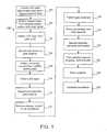
- FIG. 1is a flow diagram illustrating a first fabrication method
- FIGS. 2-10are cross-sectional side views of an exemplary double gated transistor during fabrication
- FIGS. 11-15are perspective views of an exemplary double gated transistor during fabrication
- FIG. 16is a flow diagram illustrating a second fabrication method
- FIGS. 17-24are cross-sectional side views of a second exemplary double gated transistor during fabrication.
- FIG. 25is a graph of threshold voltage versus body thickness.
- the present inventionprovides a double gated transistor and a method for forming the same that results in improved device performance and density.
- the preferred embodiment of the present inventionuses provides a double gated transistor with asymmetric gate doping, where one of the double gates is doped degenerately n-type and the other degenerately p-type.
- the threshold voltage of the resulting deviceis improved.
- the resulting transistorcan, with adequate doping of the body, have a threshold voltage in a range that enables low-voltage CMOS operation.
- a transistorcan be created that has a threshold voltage between 0V and 0.5V for nFETs and between 0 and ⁇ 0.5V for pFETs.
- the preferred embodiment of the present inventionis implemented using a fin type double gated structure.
- the double gatesare formed on each side of the body, with the body being disposed horizontally between the gates.
- the preferred method for forming this double gated transistorsallows the gate length of the device to have minimum feature size, while allowing the thickness of the body to be much smaller than the gate length. This improves control of the threshold voltage of the resulting device.
- the preferred method for forming the double gated transistoraccomplishes by using an image enhancement technique, sidewall image transfer, to define the thickness of the transistor body, allowing it to be reliably formed at sub minimum feature size.
- a fermi levelwhich, along with externally applied voltage, determines the relative affinity of the conductor for electrons (or holes).
- the fermi levelis intrinsic to the material, while in a semiconductor, such as silicon, this fermi level can be adjusted to values between the valence band and conduction band by introduction of impurities which supply excess holes or electrons.
- the two gate electrodesare doped with opposite polarity, with one gate being doped n-type and the other gate being doped p-type.
- the two gate electrodeshave different fermi levels and hence one gate electrode (the strong gate, the n-gate for nFETs) has a greater affinity for the inversion carriers while the other electrode (the weak gate, the p-gate for nFETs) has a lesser affinity for the inversion carriers.
- the inversion channelwill form in the semiconductor body at a location nearer the ‘strong’ gate, and thus results both gate electrodes contributing to the inversion potential leading to a relatively low threshold voltage (e.g, between 0 and 0.5 volts).
- Method 100forms a double gated transistor in a way that improves the threshold voltage of the transistor, while maintaining fabrication reliability and simplicity.
- the first step 101 of method 100is to provide an appropriate wafer, deposit various etch stop layers, and deposit a mandrel layer.
- the wafer usedcomprises a silicon on insulator (SOI) wafer.
- the wafercomprises a buried oxide layer beneath an SOI layer.
- the SOI layeris used to form the body of the double gated transistor.
- the doping of the SOI layeris done with an angled implant to facilitate the achievement of a uniform concentration density throughout the body.
- non-SOI waferscan be used.
- the processingremains otherwise identical to those of the SOI wafer case, except as noted.
- etch stop layersare formed on the wafer, preferably comprising a silicon dioxide layer, a silicon nitride layer, and a second silicon oxide layer. These etch stop layers will be used throughout the fabrication process when an appropriate etch stop is needed.
- the mandrel layerpreferably comprises a layer of oxide or other suitable material.
- the mandrel layeris as part of a sidewall image transfer which is used to define the body of the double gated transistor.
- the mandrel layeris used to form a sidewall spacer, which is in turn used to define the transistor body.
- the mandrel layerhas a thickness of between 10 nm and 100 nm, however, such a thickness may change depending on the desired body thickness.
- the preferred embodiment wafer portion 200comprises an SOI wafer, and as such includes an SOI layer 202 and a buried oxide layer 204 .
- an SOI layer 202On top of the SOI layer is formed a oxide layer 206 , a nitride layer 208 , and a oxide layer 210 . These layers serve as etch stop layers.
- oxide layer 210On top of oxide layer 210 is formed a mandrel layer 212 .
- the next step 102is to pattern the mandrel layer, form sidewall spacers, and pattern the etch stop layers.
- the mandrel layeris pattered to open that area in which the one of the double gates is formed.
- the sidewall spaceris preferably formed using a deposition of silicon nitride, followed by a suitable directional etch. As will be shown later, the thickness of sidewall spacer will define the body region of the double gated transistor using sidewall image transfer.
- the wafer portion 200is illustrated after the mandrel layer 212 has been patterned, a sidewall spacer 214 has been formed, and the exposed portions the etch stop layer have been removed.
- the next step 104is to pattern the SOI layer using the sidewall spacer and remaining mandrel material as a mask, and to form gate oxide on the exposed side of the SOI layer. This is preferably done using a suitable reactive ion etch.
- the gate oxideis preferably formed by thermal oxidation, typically at 750-800° C.
- an implantation into the body of the transistorcan be done. This would preferably comprise an angled implant into the exposed sidewall of the SOI layer, done before the formation of the gate oxide. This would serve to properly dope the body of the transistor. As will be described in greater detail below, this angled implant can performed in a way that achieves uniform concentration density to help compensate for threshold voltage variations.
- the wafer portion 200is illustrated after the SOI layer 202 has been patterned and gate oxide 216 has been formed on the side of the SOI layer 202 .
- an angled body implantcan also be performed before the formation of the gate oxide.
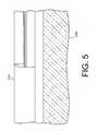
- the next step 106is to deposit and planerize the gate material.
- the double gated transistorhas one gate formed n + and another gate formed p + .
- the n + gateis formed first.
- the wafer portion 200is illustrated after n + polysilicon 218 has been deposited and planarized. As will become clear, n + polysilicon 218 will be used to form one of the gates in the preferred embodiment double gated transistor.
- the next step 108is to selectively remove the remaining mandrel layer. This is preferably done by performing a reactive ion etch of the mandrel selective to the nitride sidewall spacer, the nitride etch stop layer and the gate polysilicon. Then an intermediate oxide layer is formed on the polysilicon gate material, preferably by growing thermal oxide on the polysilicon gate.
- FIG. 6the wafer portion 200 is illustrated after the mandrel layer 212 has been removed, oxide etch stop layer 210 has been removed, and a thermal oxide layer 220 has been formed on the gate polysilicon 218 .
- the nitride layer 208 that was beneath the remaining mandrel layeris etched selectively to the oxide 220 followed by a brief HF etch which removes the remaining oxide layer 206 which was beneath the remaining mandrel layer.
- the next step 110is to etch the exposed SOI layer. This is preferably done by using a reactive ion etch that etches the SOI layer, stopping on the buried oxide layer. This completes the patterning of the SOI layer to defines the thickness of the body of the double gated transistor. Then a gate oxide is formed on the exposed side of the transistor body.
- this stepanother implantation into the body of the transistor can be performed.
- Thiswould again preferably comprise an angled implant into the exposed sidewall of the SOI layer, done before the formation of the gate oxide.
- the wafer portion 200is illustrated after the patterning of the SOI layer 202 .
- the remaining portion of SOI layer 202comprises the body of the double gated transistor.
- Gate oxide 221is formed on the exposed SOI layer 202 using a thermal oxidation or by depositing a dielectric film.
- a deposit/etch oxide processis used to deposit silicon dioxide exclusively on the bottom horizontal surfaces of the etched silicon of thickness approximately one-quarter the height of the etched fins.
- the oxidemay be doped with boron in the case of nFETs or phosphorus in the case of pFETs and some portion of the dopant out diffused into those portions of the fins immediately adjacent to the doped oxide. This serves to suppress leakage in what will be ungated surfaces of the fins, from source to drain.
- the patterning of the SOI layerhas defined the body of the double gated transistor. It is generally desirable to have the body thickness, illustrated as T SI , narrow when compared to the gate length. Typically, the body thickness should be less than one quarter of the gate length to give good threshold voltage control. Also, it is generally desirable that the body thickness should be greater than 2.5 nm to avoid degraded mobility due to quantum confinement issues. As the gate length is generally made to minimum feature size, sidewall image transfer is used to achieve the subminimum feature size of the body. Thus, as illustrated and described above, the width of the sidewall spacer determines the body thickness.
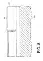
- the next step 112is to deposit and planerize the gate material for the second gate.
- the preferred embodimentuses gate material of opposite doping to form the two gates.
- the preferred embodimentuses p+ doped polysilicon to form the second of the two gates.
- the planarization of the p+ polysilicon gate materialstops on the thermally grown oxide previously formed on the n+ polysilicon gate.
- a second layer of thermally grown oxideis formed.
- FIG. 8the wafer portion 202 is illustrated after the deposition and planarization of p+ doped polysilicon 226 to form the second gate. Thermally grown oxide 228 is then formed on the deposited polysilicon 226 .
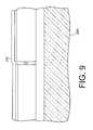
- the next step 114is to remove the sidewall spacer, and fill the sidewall spacer opening with intrinsic polysilicon, to maximize silicide formation in this region later on in the process.
- the sidewall spacermay be left in place if the separate, independent gate contacts are desirable.
- the intrinsic polysiliconis then planarized using a CMP process that stops on the two layers of thermally grown oxide. This planarization process does not require high selectivity because there is very little excess intrinsic polysilicon to remove.
- the exposed thermally grown oxide on the two gatesis then removed using a similar planarization process. Again, high selectivity is not required for this processing step. Turning now to FIG.
- the wafer portion 200is illustrated after the remaining portion of the sidewall spacer 214 has been removed, and then the space is filled with intrinsic polysilicon 230 .
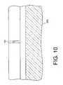
- FIG. 10then illustrates the wafer portion 200 after the excess polysilicon 230 and thermally grown oxide 220 and 228 have been removed by CMP process. This leaves only a small portion of the intrinsic polysilicon 230 in the place of the originally formed sidewall spacer. This portion of intrinsic polysilicon 230 will be used to allow the formation of a silicide bridge connecting the p+ and n+ polysilicon gates later in the process flow.
- the next step 116is to pattern the gates. This involves selectively removing the portions of the gate materials that exist in adjacent the source and drain regions of the transistor. This is preferably done using standard lithographic techniques, i.e, depositing and patterning a hardmask, and then using the patterned hardmask as an etch block during an etching of the gate materials.
- the hardmaskis preferably a nitride hardmask, as that is the same as the already formed etch stop layer on the body.
- FIG. 11the wafer portion 200 is illustrated in perspective form.
- a nitride hardmask 232has been formed extending across the two gates, which comprise n+ gate polysilicon 218 and p+ gate polysilicon 226 .
- FIG. 12the wafer portion 200 is illustrated after gate polysilicon 218 and gate polysilicon 226 have been patterned using an etch selective to the hardmask.
- the patterningpreferably removes all the gate polysilicon down to the buried oxide layer 204 .
- the patterning of the gatesis preferably done using a directional etch that is selective to nitride.
- the patterningdoes not remove the portions of the SOI body 202 that are protected by the previously formed nitride etch stop layer 208 .
- the patterningleaves a portion of n+ polysilicon 218 and p+ polysilicon 226 , which defines the two gates of the double gated transistor.
- a buffered HF clean upis performed, followed by a thermal reoxidation designed to grow oxide on all the exposed silicon surfaces. This preferably forms a thin 50 angstrom film of oxide that provides good interface when the gate meets the body.
- the next step 118 in method 100is to form source, drain, and halo implants in the transistor.
- these implantsare made into all four directions of the body, to ensure that a uniform implant is made into both sides of the body.
- both the source and drain implantsare made from both sides of the source and drain portion of the body.
- another implantis made, with a different implant energies and angles, to form the halo implants that improve short channel effects.
- the halo implantsare performed at higher energies and at angles more acute with respect to the fin in order to assure placement of the halo dopant further under the gate electrodes than the source/drain dopants.
- typically arsenicis used for the source/drain implants in the range of 1 to 5 keV and a dose of 5 ⁇ 10 14 to 2 ⁇ 10 15 cm ⁇ 3 with angles between 75° and 80° with respect to the fins
- boronis used for the halo implants with energies in the range of 5 to 15 keV and a dose of 1 ⁇ 10 13 to 8 ⁇ 10 3 cm ⁇ 3 with the halo oriented between 20° and 30° with respect to the fins.
- typically boronis used for the source/drain implants in the range of 0.5 to 3 keV and dose of 5 ⁇ 10 14 to 2 ⁇ 10 15 cm ⁇ 3 with angles between 75° and 80° with respect to the fins, and arsenic used for the halos, with energies from 20 to 45 keV and dose of 1 ⁇ 10 13 to 8 ⁇ 10 13 cm ⁇ 3 with the halo oriented between 20° and 30° with respect to the fins.
- all of the above implantsmust be suitable angles from the azimuth of the wafer, typically between 7° to 30° from azimuth.
- the next step 120is to deposit dielectric of thickness greater than the height of the combined gate electrode and hardmask above the BOX, covering the entire gate electrodes and exposed fins, planerize and partially recess until a portion (typically 10 to 50 nm) of the hardmask and gate electrode, but not any of the source/drain fin region, is exposed. As will become clear, this step is part of the formation of sidewall spacers at the edges of the transistor gate.
- the dielectric usedpreferably comprises oxide, which can be etched selective to the nitride hardmask already formed.
- FIG. 13the wafer portion 200 is illustrated after dielectric 240 has been deposited, surrounding the transistor gate electrode, planarized and then recessed. The dielectric is preferably recessed using a directional etch selective to the previously provided nitride hardmask 232 .
- the next step 122is to form sidewall spacers on the edges of the gates, and etch the previously deposited dielectric. This is preferably done using a conformal deposition of a dielectric material, followed by a directional etch.
- the sidewall spacersare preferably formed of nitride. The nitride sidewall spacers, together with the nitride hardmask, can then be used to mask a directional etch and thereby remove the oxide except adjacent to the gates.
- the wafer portion 200is illustrated after nitride sidewall spacers 242 have been formed, and the dielectric 240 etched away, leaving only sidewall portions 244 adjacent the transistor gates.
- the hardmask 232 , the sidewall spacers 242 , and the sidewall portions 244combine to effectively isolate the gate from the source and drain contacts, which are formed next.
- the next step 124is to form source and drain contacts. This is preferably done by filling the previously removed areas with contact material.
- the contact materialcan be a selective deposition of silicon, tungsten or other conductive material which makes low-resistance contacts to n+ and/or p+ silicon. If silicon is used, it is doped degenerately n+ or p+ for nFETs or pFETs, respectively. The material can be deposited until it covers the wafer to a height above the height of the nitride hardmask and then planarized by RIE and/or chemical-mechanical polish until the nitride hardmask is completely exposed. Next, as illustrated in FIG.
- the waferis patterned with a mask which is used to etch unwanted portions of the source/drain contact material to both isolate source from drain and to isolate a plurality of such FETs from each other.
- the hardmaskmay be selectively removed by RIE or other etching techniques such as hot phosphoric acid, and a metal such as cobalt or titanium deposited and sintered at approximately 700° C. to form metal silicide over the gate, and in the case of silicon contacts, over the source and drain contacts as well.
- step 301the wafer is prepared, etch stop layers and a mandrel layer is formed in as in step 101 of the method 100 described above. Then in step 302 , the mandrel layer is patterned and the etch stop layers are directly etched. This differs from method 100 in that no sidewall spacer is formed on the mandrel layer before the etch stop layers are patterned.
- step 302the wafer portion 200 is illustrated after the formation of the etch stop layers, the mandrel layer, and the etching of the mandrel layer and etch stop layers directly.
- the next step 304is to pattern the SOI layer using the remaining mandrel layer as a mask, and to form gate oxide on the exposed side of the SOI layer. This is preferably done using a suitable reactive ion etch, followed by a thermal oxidation, typically at between 750° C. and 800° C., or by CVD deposition of a high-k material such as aluminum oxide. Also, during this step, an implantation into the body of the transistor can be done. This would preferably comprise an angled implant into the exposed sidewall of the SOI layer, done before the formation of the gate oxide. This implant serves to properly dope the body of the transistor. As will be described in greater detail below, this implant can be performed in a way that achieves uniform concentration density to help compensate for threshold voltage variations that would otherwise result from variations in body thickness.
- the wafer portion 200is illustrated after the SOI layer 202 has been patterned and gate oxide 216 has been formed on the side of the SOI layer 202 .
- an angled body implantcan also be performed before the formation of the gate oxide.
- the next step 306is to deposit and planerize the gate material.
- the double gated transistorhas one gate formed n+ and the other gate formed p+.
- the gate n+ gateis formed first.
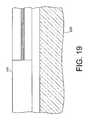
- FIG. 19the wafer portion 200 is illustrated after n+ polysilicon 218 has been deposited and planarized. As will become clear, n+ polysilicon will be used to form one of the gates in the preferred embodiment double gated transistor.
- the next step 308is to remove the remaining mandrel material, form a sidewall spacer along the edge of the remaining first gate material, and form an intermediate oxide layer on the polysilicon gate material.
- the intermediate oxide layeris formed by growing thermal oxide on the polysilicon gate.
- FIG. 20the wafer portion 200 is illustrated after the mandrel layer 212 has been removed, the sidewall spacer 302 formed on the sidewall of the first gate material, and a thermal oxide layer 220 has been form on the gate polysilicon 218 .
- the nitride layer 208 that was beneath the remaining mandrel layeris etched selectively to the oxide 220 followed by a brief HF etch which removes the remaining oxide layer 206 which was beneath the remaining mandrel layer.
- the next step 310is to etch the exposed SOI layer. This is preferably done by using a reactive ion etch that etches the SOI layer, stopping on the buried oxide layer. This completes the patterning of the SOI layer to define the thickness of the body of the double gated transistor. Gate oxide is then formed on the exposed side of the transistor body. Again, during this step a implantation into the body of the transistor can be performed. This would again preferably comprise an angled implant into the exposed sidewall of the SOI layer, done before the formation of the gate oxide.
- the wafer portion 200is illustrated after the patterning of the SOI layer 202 .
- the remaining portion of the SOI layer 202comprises the body of the doubled gated transistor.
- Gate oxide 221is formed on the exposed SOI layer 202 using a thermal oxidation or by depositing a dielectric film.
- the next step 312is to deposit and planerize the gate material for the second gate.
- the preferred embodimentuses gate material of opposite doping to form the two gates.
- the preferred embodimentuses p+ doped polysilicon to form the second of the two gates.
- the planarization of the p+ polysilicon gate materialstops on the thermally grown oxide previously formed on the n+ polysilicon gate.
- a second layer of thermally grown oxideis formed.
- FIG. 22the wafer portion 202 is illustrated after the deposition and planarization of p+ doped polysilicon 226 to form the second gate. Thermally grown oxide 228 is then formed on the deposited polysilicon 226 .
- the next step 314is to remove the sidewall spacer, and fill the sidewall spacer opening with intrinsic polysilicon, to maximize silicide formation in this region later on in the process.
- the sidewall spacermay be left in place if the separate, independent gate contacts are desirable.
- the intrinsic polysiliconis then planarized using a CMP process that stops on the two layers of thermally grown oxide. This planarization process does not require high selectivity because there is very little excess intrinsic polysilicon to remove.
- the exposed thermally grown oxide on the two gatesis then removed using a similar planarization process. Again, high selectivity is not required for this processing step. Turning now to FIG.
- the wafer portion 200is illustrated after the remaining portion of the sidewall spacer 302 has been removed, and then the space is filled with intrinsic polysilicon 230 .
- FIG. 24then illustrates the wafer portion 200 after the excess polysilicon 230 and thermally grown oxide 220 and 228 have been removed by CMP process. This leaves only a small portion of the intrinsic polysilicon 230 in the place of the originally formed sidewall spacer. This portion of intrinsic polysilicon 230 will be used to allow the formation of a silicide bridge connecting the p+ and n+ polysilicon gates later in the process flow.
- method 300has the advantage of resulting in minimal erosion of the sidewall spacer used to define the transistor body since the spacer is now exposed to reactive ion etching only once. Consequently the silicon etch profiles achieved with this embodiment are very well controlled.
- stepsare taken to compensate for threshold voltage variations that would normally arise due to variations in body thickness.
- the threshold voltageis at least partially dependent upon the thickness of the body.
- the thickness of the bodyis mostly determined by the thickness of the sidewall spacer used to define the body during sidewall image transfer.
- the process for forming sidewall spacerscan result in some variation in the thickness of the sidewall spacer.
- this threshold voltage variationwill be within tolerable limits. However, in some cases it may be desirable to compensate for these variations.
- a uniform doping of the bodyis performed to compensate for the thickness differences. It is generally desirable in this embodiment to make the doping uniform in the three dimension sense, as opposed to a doping scheme that results in uniform dopant amounts, with densities that vary with body thickness. This is done by making an implant that results in a constant, uniform dopant concentration density in the body. Preferably this is done by making several angled implants into the body when the side of the body is exposed. For example, an implant can be made when one side is exposed (as illustrated in FIG. 4 ) and second implant made when the other side is (as illustrated in FIG. 7 ) For, example, a uniform fin doping can be achieved by implanting the exposed sidewalls of silicon in FIG.
- this uniform concentrationis made by performing a perpendicular implant prior to the formation of the etch stop layers and the mandrel layers.
- a perpendicular implantprior to the formation of the etch stop layers and the mandrel layers.
- substantially uniform doping concentrationis achieved.
- multiple perpendicular implantscan be used to achieve this uniformity.
- pFETs and nFETswould need to be separately masked and implanted, with phosphorus or arsenic used for pFETs and boron for nFETs.
- VtToxs + ⁇ Toxs + Toxw - T si ⁇ ⁇ ox ⁇ si ⁇ Eg + ⁇ ms + Toxs ⁇ Q e ⁇ ox ⁇ N A ⁇ T si 2 Eq .
- ⁇ siis the permittivity of silicon
- Egis the band-gap energy of silicon ( ⁇ 1.1 eV)
- Tsiis the body thickness
- ⁇is the depth of the charge centroid of the inversion layer in the silicon body beneath the surface adjacent to the strong gate ( ⁇ 1 nm)
- Q eis the charge of the electron
- N ais the doping density of the body (or fin)
- ⁇ msis the fermi level of the gate electrode relative to that of the inversion layer, when formed
- ⁇ 0xis the permittivity of the gate dielectric
- Toxsis the thickness of the insulator with the gate electrode of the fermi level more attractive to the inversion channel carriers (the n+ electrode in an nFET, the p+ electrode in a pFET)
- Toxwis the insulator thickness of the insulator with the gate electrode of the fermi level less attractive to the inversion channel carriers (the p+ electrode for an nFET and the n+ electrode
- a graphis illustrating the threshold voltage (V T ) plotted against body thickness (T SI ) for a regular, uncompensated double gated transistor and a for a double gated transistor that has been compensated for threshold voltage variations by providing a more uniform doping concentration.
- the threshold voltage of a double gated transistor where the body has been dopeduniformly exhibits less variation as a function of body thickness.
- the uniform concentration density doping of the bodyhelps compensate for body thickness variations that would normally greatly affect the threshold voltage.
- the present inventionprovides a double gated transistor and a method for forming the same that results in improved device performance and density.
- the preferred embodiment of the present inventionuses provides a double gated transistor with asymmetric gate doping, where one of the double gates is doped degenerately n-type and the other degenerately p-type. By doping one of the gates n-type, and the other p-type, the threshold voltage of the resulting device is improved. In particular, by asymmetrically doping the two gates, the resulting transistor can, with adequate doping of the body, have a threshold voltage in a range that enables low-voltage CMOS operation.
Landscapes
- Thin Film Transistor (AREA)
- Metal-Oxide And Bipolar Metal-Oxide Semiconductor Integrated Circuits (AREA)
- Insulated Gate Type Field-Effect Transistor (AREA)
Abstract
Description
- 1. Technical Field
- The present invention relates generally to the field of semiconductor manufacturing and, more specifically, to a method for forming double gated field effect transistors.
- 2. Background Art
- The need to remain cost and performance competitive in the production of semiconductor devices has caused continually increasing device density in integrated circuits. To facilitate the increase in device density, new technologies are constantly needed to allow the feature size of these semiconductor devices to be reduced.
- The push for ever increasing device densities is particularly strong in CMOS technologies, such as the in the design and fabrication of field effect transistors (FETs). FETs are used in almost all types of integrated circuit design (i.e., microprocessors, memory, etc.) Unfortunately, increased device density in CMOS FET often results in degradation of performance and/or reliability.
- One type of FET that has been proposed to facilitate increased device density is a double gated field effect transistor. Double gated FETs use two gates, one on each side of the body, to facilitate scaling of CMOS dimensions while maintaining an acceptable performance. In particular, the use of the double gate increases the gate area, which allows the transistor to have better current control, without increasing the gate length of the device. As such, the double gated FET is able to have the current control of a larger transistor without requiring the device space of the larger transistor.
- Unfortunately, several difficulties arise in the design and fabrication of double gated CMOS transistors. First, the relative dimensions of a double gated transistor are such that it is difficult to reliably fabricate one that has a reliable performance and minimum feature size. Second, the threshold voltage of a double gated transistor is highly dependent upon the material used for the two gates. In particular, current fabrication techniques have generally resulted in a double gated transistor that has either too high a threshold voltage, or too low of a threshold voltage. For example, if the gates are doped the same polarity as the source, the threshold voltage will generally be near zero. Conversely, if the gates are doped the opposite polarity of the source, then the threshold voltage will be approximately one volt. Neither result is desirable in most CMOS applications.
- Thus, there is a need for improved device structures and methods of fabrications of double gated CMOS devices that provide improved threshold voltage of the resulting double gated CMOS without overly increasing fabrication complexity.
- Accordingly, the present invention provides a double gated transistor and a method for forming the same that results in improved device performance and density. The preferred embodiment of the present invention uses provides a double gated transistor with asymmetric gate doping, where one of the double gates is doped degenerately n-type and the other degenerately p-type. By doping one of the gates n-type, and the other p-type, the threshold voltage of the resulting device is improved. In particular, by asymeterically doping the two gates, the resulting transistor can, with adequate doping of the body, have a threshold voltage in a range that enables low-voltage CMOS operation. For example, a transistor can be created that has a threshold voltage between 0V and 0.5V for nFETs and between 0 and −0.5V for pFETs.
- The preferred embodiment of the present invention is implemented using a fin type double gated structure. In a fin type structure, the double gates are formed on each side of the body, with the body being disposed horizontally between the gates. The preferred method for forming this double gated transistors allows the gate length of the device to have minimum feature size, while allowing the thickness of the body to be much smaller than the gate length. This improves control of the threshold voltage of the resulting device. The preferred method for forming the double gated transistor accomplishes by using an image enhancement technique, sidewall image transfer, to define the thickness of the transistor body, allowing it to be reliably formed at sub minimum feature size.
- The foregoing and other advantages and features of the invention will be apparent from the following more particular description of a preferred embodiment of the invention, as illustrated in the accompanying drawings.
- The preferred exemplary embodiment of the present invention will hereinafter be described in conjunction with the appended drawings, where like designations denote like elements, and
FIG. 1 is a flow diagram illustrating a first fabrication method;FIGS. 2-10 are cross-sectional side views of an exemplary double gated transistor during fabrication;FIGS. 11-15 are perspective views of an exemplary double gated transistor during fabrication;FIG. 16 is a flow diagram illustrating a second fabrication method;FIGS. 17-24 are cross-sectional side views of a second exemplary double gated transistor during fabrication; andFIG. 25 is a graph of threshold voltage versus body thickness.- Accordingly, the present invention provides a double gated transistor and a method for forming the same that results in improved device performance and density. The preferred embodiment of the present invention uses provides a double gated transistor with asymmetric gate doping, where one of the double gates is doped degenerately n-type and the other degenerately p-type. By doping one of the gates n-type, and the other p-type, the threshold voltage of the resulting device is improved. In particular, by asymmetrically doping the two gates, the resulting transistor can, with adequate doping of the body, have a threshold voltage in a range that enables low-voltage CMOS operation. For example, a transistor can be created that has a threshold voltage between 0V and 0.5V for nFETs and between 0 and −0.5V for pFETs.
- The preferred embodiment of the present invention is implemented using a fin type double gated structure. In a fin type structure, the double gates are formed on each side of the body, with the body being disposed horizontally between the gates. The preferred method for forming this double gated transistors allows the gate length of the device to have minimum feature size, while allowing the thickness of the body to be much smaller than the gate length. This improves control of the threshold voltage of the resulting device. The preferred method for forming the double gated transistor accomplishes by using an image enhancement technique, sidewall image transfer, to define the thickness of the transistor body, allowing it to be reliably formed at sub minimum feature size.
- Various electrically conducting materials have associated with them a built-in electrical potential, often referred to as a fermi level, which, along with externally applied voltage, determines the relative affinity of the conductor for electrons (or holes). In a metal, the fermi level is intrinsic to the material, while in a semiconductor, such as silicon, this fermi level can be adjusted to values between the valence band and conduction band by introduction of impurities which supply excess holes or electrons. In the asymmetric double gated FET of the preferred embodiment, the two gate electrodes are doped with opposite polarity, with one gate being doped n-type and the other gate being doped p-type. Thus, the two gate electrodes have different fermi levels and hence one gate electrode (the strong gate, the n-gate for nFETs) has a greater affinity for the inversion carriers while the other electrode (the weak gate, the p-gate for nFETs) has a lesser affinity for the inversion carriers. As a result the inversion channel will form in the semiconductor body at a location nearer the ‘strong’ gate, and thus results both gate electrodes contributing to the inversion potential leading to a relatively low threshold voltage (e.g, between 0 and 0.5 volts).
- Turning now to
FIG. 1 , amethod 100 for forming a double gated transistor in accordance with the preferred embodiment is illustrated.Method 100 forms a double gated transistor in a way that improves the threshold voltage of the transistor, while maintaining fabrication reliability and simplicity. - The
first step 101 ofmethod 100 is to provide an appropriate wafer, deposit various etch stop layers, and deposit a mandrel layer. In the preferred embodiment, the wafer used comprises a silicon on insulator (SOI) wafer. As such, the wafer comprises a buried oxide layer beneath an SOI layer. As will be come clear, the SOI layer is used to form the body of the double gated transistor. As such, it is generally preferable to use a SOI layer that has a p-type (for NFETs) doping density in the range of 3×1018cm−3to 8×1018cm−3to provide proper centering and control of the threshold voltage of the transistor. However, in another embodiment to be described later, the doping of the SOI layer is done with an angled implant to facilitate the achievement of a uniform concentration density throughout the body. - However, non-SOI wafers can be used. When a non-SOI wafer is used, the processing remains otherwise identical to those of the SOI wafer case, except as noted.
- With a SOI wafer provided, three etch stop layers are formed on the wafer, preferably comprising a silicon dioxide layer, a silicon nitride layer, and a second silicon oxide layer. These etch stop layers will be used throughout the fabrication process when an appropriate etch stop is needed.
- Next, a mandrel layer is formed. The mandrel layer preferably comprises a layer of oxide or other suitable material. As will be explained in greater detail later, the mandrel layer is as part of a sidewall image transfer which is used to define the body of the double gated transistor. As such, the mandrel layer is used to form a sidewall spacer, which is in turn used to define the transistor body. In the preferred embodiment, the mandrel layer has a thickness of between 10 nm and 100 nm, however, such a thickness may change depending on the desired body thickness.
- Turning now to
FIG. 2 , awafer portion 200 is illustrated after the formation of etch stop layers and a mandrel layer. The preferredembodiment wafer portion 200 comprises an SOI wafer, and as such includes anSOI layer 202 and a buriedoxide layer 204. On top of the SOI layer is formed aoxide layer 206, anitride layer 208, and aoxide layer 210. These layers serve as etch stop layers. On top ofoxide layer 210 is formed amandrel layer 212. - Returning to
FIG. 1 , thenext step 102 is to pattern the mandrel layer, form sidewall spacers, and pattern the etch stop layers. The mandrel layer is pattered to open that area in which the one of the double gates is formed. The sidewall spacer is preferably formed using a deposition of silicon nitride, followed by a suitable directional etch. As will be shown later, the thickness of sidewall spacer will define the body region of the double gated transistor using sidewall image transfer. - Turning to
FIG. 3 , thewafer portion 200 is illustrated after themandrel layer 212 has been patterned, asidewall spacer 214 has been formed, and the exposed portions the etch stop layer have been removed. - Returning to
FIG. 1 , thenext step 104 is to pattern the SOI layer using the sidewall spacer and remaining mandrel material as a mask, and to form gate oxide on the exposed side of the SOI layer. This is preferably done using a suitable reactive ion etch. The gate oxide is preferably formed by thermal oxidation, typically at 750-800° C. Also, during this step an implantation into the body of the transistor can be done. This would preferably comprise an angled implant into the exposed sidewall of the SOI layer, done before the formation of the gate oxide. This would serve to properly dope the body of the transistor. As will be described in greater detail below, this angled implant can performed in a way that achieves uniform concentration density to help compensate for threshold voltage variations. - Turning now to
FIG. 4 , thewafer portion 200 is illustrated after theSOI layer 202 has been patterned andgate oxide 216 has been formed on the side of theSOI layer 202. Again, an angled body implant can also be performed before the formation of the gate oxide. - Returning to
FIG. 1 , thenext step 106 is to deposit and planerize the gate material. As described above, in the preferred embodiment, the double gated transistor has one gate formed n+ and another gate formed p+. In the illustrated implantation, the n+ gate is formed first. Turning toFIG. 5 , thewafer portion 200 is illustrated after n+ polysilicon218 has been deposited and planarized. As will become clear, n+ polysilicon218 will be used to form one of the gates in the preferred embodiment double gated transistor. - The
next step 108 is to selectively remove the remaining mandrel layer. This is preferably done by performing a reactive ion etch of the mandrel selective to the nitride sidewall spacer, the nitride etch stop layer and the gate polysilicon. Then an intermediate oxide layer is formed on the polysilicon gate material, preferably by growing thermal oxide on the polysilicon gate. Turning now toFIG. 6 , thewafer portion 200 is illustrated after themandrel layer 212 has been removed, oxideetch stop layer 210 has been removed, and athermal oxide layer 220 has been formed on thegate polysilicon 218. Thenitride layer 208 that was beneath the remaining mandrel layer is etched selectively to theoxide 220 followed by a brief HF etch which removes the remainingoxide layer 206 which was beneath the remaining mandrel layer. - The
next step 110 is to etch the exposed SOI layer. This is preferably done by using a reactive ion etch that etches the SOI layer, stopping on the buried oxide layer. This completes the patterning of the SOI layer to defines the thickness of the body of the double gated transistor. Then a gate oxide is formed on the exposed side of the transistor body. - Also, during this step another implantation into the body of the transistor can be performed. This would again preferably comprise an angled implant into the exposed sidewall of the SOI layer, done before the formation of the gate oxide.
- Turning to
FIG. 7 , thewafer portion 200 is illustrated after the patterning of theSOI layer 202. The remaining portion ofSOI layer 202 comprises the body of the double gated transistor.Gate oxide 221 is formed on the exposedSOI layer 202 using a thermal oxidation or by depositing a dielectric film. - When a non-SOI wafer is used, after the silicon fins are etched by time to the desired depth (typically 100-200 nm below the original silicon surface) a deposit/etch oxide process is used to deposit silicon dioxide exclusively on the bottom horizontal surfaces of the etched silicon of thickness approximately one-quarter the height of the etched fins. The oxide may be doped with boron in the case of nFETs or phosphorus in the case of pFETs and some portion of the dopant out diffused into those portions of the fins immediately adjacent to the doped oxide. This serves to suppress leakage in what will be ungated surfaces of the fins, from source to drain.
- Returning to the SOI embodiment, it should be noted that the patterning of the SOI layer has defined the body of the double gated transistor. It is generally desirable to have the body thickness, illustrated as TSI, narrow when compared to the gate length. Typically, the body thickness should be less than one quarter of the gate length to give good threshold voltage control. Also, it is generally desirable that the body thickness should be greater than 2.5 nm to avoid degraded mobility due to quantum confinement issues. As the gate length is generally made to minimum feature size, sidewall image transfer is used to achieve the subminimum feature size of the body. Thus, as illustrated and described above, the width of the sidewall spacer determines the body thickness.
- The
next step 112 is to deposit and planerize the gate material for the second gate. As discussed above, the preferred embodiment uses gate material of opposite doping to form the two gates. Thus, the preferred embodiment uses p+ doped polysilicon to form the second of the two gates. The planarization of the p+ polysilicon gate material stops on the thermally grown oxide previously formed on the n+ polysilicon gate. After the planarization of the p+ polysilicon, a second layer of thermally grown oxide is formed. Turning now toFIG. 8 , thewafer portion 202 is illustrated after the deposition and planarization of p+doped polysilicon 226 to form the second gate. Thermallygrown oxide 228 is then formed on the depositedpolysilicon 226. - The
next step 114 is to remove the sidewall spacer, and fill the sidewall spacer opening with intrinsic polysilicon, to maximize silicide formation in this region later on in the process. Optionally, the sidewall spacer may be left in place if the separate, independent gate contacts are desirable. The intrinsic polysilicon is then planarized using a CMP process that stops on the two layers of thermally grown oxide. This planarization process does not require high selectivity because there is very little excess intrinsic polysilicon to remove. The exposed thermally grown oxide on the two gates is then removed using a similar planarization process. Again, high selectivity is not required for this processing step. Turning now toFIG. 9 , thewafer portion 200 is illustrated after the remaining portion of thesidewall spacer 214 has been removed, and then the space is filled withintrinsic polysilicon 230.FIG. 10 then illustrates thewafer portion 200 after theexcess polysilicon 230 and thermally grownoxide intrinsic polysilicon 230 in the place of the originally formed sidewall spacer. This portion ofintrinsic polysilicon 230 will be used to allow the formation of a silicide bridge connecting the p+ and n+ polysilicon gates later in the process flow. - Returning to
method 100, thenext step 116 is to pattern the gates. This involves selectively removing the portions of the gate materials that exist in adjacent the source and drain regions of the transistor. This is preferably done using standard lithographic techniques, i.e, depositing and patterning a hardmask, and then using the patterned hardmask as an etch block during an etching of the gate materials. The hardmask is preferably a nitride hardmask, as that is the same as the already formed etch stop layer on the body. - Turning now to
FIG. 11 , thewafer portion 200 is illustrated in perspective form. Anitride hardmask 232 has been formed extending across the two gates, which comprise n+gate polysilicon 218 andp+ gate polysilicon 226. Turning now toFIG. 12 , thewafer portion 200 is illustrated aftergate polysilicon 218 andgate polysilicon 226 have been patterned using an etch selective to the hardmask. The patterning preferably removes all the gate polysilicon down to the buriedoxide layer 204. The patterning of the gates is preferably done using a directional etch that is selective to nitride. Thus, the patterning does not remove the portions of theSOI body 202 that are protected by the previously formed nitrideetch stop layer 208. The patterning leaves a portion ofn+ polysilicon 218 andp+ polysilicon 226, which defines the two gates of the double gated transistor. - In the preferred embodiment a buffered HF clean up is performed, followed by a thermal reoxidation designed to grow oxide on all the exposed silicon surfaces. This preferably forms a thin 50 angstrom film of oxide that provides good interface when the gate meets the body.
- The
next step 118 inmethod 100 is to form source, drain, and halo implants in the transistor. Preferably these implants are made into all four directions of the body, to ensure that a uniform implant is made into both sides of the body. In particular, both the source and drain implants are made from both sides of the source and drain portion of the body. Then another implant is made, with a different implant energies and angles, to form the halo implants that improve short channel effects. The halo implants are performed at higher energies and at angles more acute with respect to the fin in order to assure placement of the halo dopant further under the gate electrodes than the source/drain dopants. For nFETs, typically arsenic is used for the source/drain implants in the range of 1 to 5 keV and a dose of 5×10¹⁴to 2×1015cm−3with angles between 75° and 80° with respect to the fins, and boron is used for the halo implants with energies in the range of 5 to 15 keV and a dose of 1×10¹³to 8×103cm−3with the halo oriented between 20° and 30° with respect to the fins. Similarly, for pFETs, typically boron is used for the source/drain implants in the range of 0.5 to 3 keV and dose of 5×10¹⁴to 2×1015cm−3with angles between 75° and 80° with respect to the fins, and arsenic used for the halos, with energies from 20 to 45 keV and dose of 1×10¹³to 8×1013cm−3with the halo oriented between 20° and 30° with respect to the fins. Furthermore, all of the above implants must be suitable angles from the azimuth of the wafer, typically between 7° to 30° from azimuth. - The
next step 120 is to deposit dielectric of thickness greater than the height of the combined gate electrode and hardmask above the BOX, covering the entire gate electrodes and exposed fins, planerize and partially recess until a portion (typically 10 to 50 nm) of the hardmask and gate electrode, but not any of the source/drain fin region, is exposed. As will become clear, this step is part of the formation of sidewall spacers at the edges of the transistor gate. The dielectric used preferably comprises oxide, which can be etched selective to the nitride hardmask already formed. Turning now toFIG. 13 , thewafer portion 200 is illustrated afterdielectric 240 has been deposited, surrounding the transistor gate electrode, planarized and then recessed. The dielectric is preferably recessed using a directional etch selective to the previously providednitride hardmask 232. - The
next step 122 is to form sidewall spacers on the edges of the gates, and etch the previously deposited dielectric. This is preferably done using a conformal deposition of a dielectric material, followed by a directional etch. The sidewall spacers are preferably formed of nitride. The nitride sidewall spacers, together with the nitride hardmask, can then be used to mask a directional etch and thereby remove the oxide except adjacent to the gates. - Turning now to
FIG. 14 , thewafer portion 200 is illustrated afternitride sidewall spacers 242 have been formed, and the dielectric240 etched away, leaving only sidewallportions 244 adjacent the transistor gates. Thehardmask 232, thesidewall spacers 242, and thesidewall portions 244 combine to effectively isolate the gate from the source and drain contacts, which are formed next. - The
next step 124 is to form source and drain contacts. This is preferably done by filling the previously removed areas with contact material. The contact material can be a selective deposition of silicon, tungsten or other conductive material which makes low-resistance contacts to n+ and/or p+ silicon. If silicon is used, it is doped degenerately n+ or p+ for nFETs or pFETs, respectively. The material can be deposited until it covers the wafer to a height above the height of the nitride hardmask and then planarized by RIE and/or chemical-mechanical polish until the nitride hardmask is completely exposed. Next, as illustrated inFIG. 15 , the wafer is patterned with a mask which is used to etch unwanted portions of the source/drain contact material to both isolate source from drain and to isolate a plurality of such FETs from each other. Finally, the hardmask may be selectively removed by RIE or other etching techniques such as hot phosphoric acid, and a metal such as cobalt or titanium deposited and sintered at approximately 700° C. to form metal silicide over the gate, and in the case of silicon contacts, over the source and drain contacts as well. - Turning now to
FIG. 16 , a alternativepreferred embodiment method 300 is illustrated. This method has. the advantage of resulting in minimal erosion of the sidewall spacer used to define the transistor body since the spacer is now exposed to reactive ion etching only once. Consequently the silicon etch profiles achieved with this embodiment are very well controlled. Instep 301, the wafer is prepared, etch stop layers and a mandrel layer is formed in as instep 101 of themethod 100 described above. Then instep 302, the mandrel layer is patterned and the etch stop layers are directly etched. This differs frommethod 100 in that no sidewall spacer is formed on the mandrel layer before the etch stop layers are patterned. Turning toFIG. 17 , thewafer portion 200 is illustrated after the formation of the etch stop layers, the mandrel layer, and the etching of the mandrel layer and etch stop layers directly. - The
next step 304 is to pattern the SOI layer using the remaining mandrel layer as a mask, and to form gate oxide on the exposed side of the SOI layer. This is preferably done using a suitable reactive ion etch, followed by a thermal oxidation, typically at between 750° C. and 800° C., or by CVD deposition of a high-k material such as aluminum oxide. Also, during this step, an implantation into the body of the transistor can be done. This would preferably comprise an angled implant into the exposed sidewall of the SOI layer, done before the formation of the gate oxide. This implant serves to properly dope the body of the transistor. As will be described in greater detail below, this implant can be performed in a way that achieves uniform concentration density to help compensate for threshold voltage variations that would otherwise result from variations in body thickness. - Turning now to
FIG. 18 , thewafer portion 200 is illustrated after theSOI layer 202 has been patterned andgate oxide 216 has been formed on the side of theSOI layer 202. Again, an angled body implant can also be performed before the formation of the gate oxide. - Returning to
FIG. 16 , thenext step 306 is to deposit and planerize the gate material. As described above, in the preferred embodiment, the double gated transistor has one gate formed n+ and the other gate formed p+. In the illustrated embodiment, the gate n+ gate is formed first. Turning toFIG. 19 , thewafer portion 200 is illustrated after n+polysilicon 218 has been deposited and planarized. As will become clear, n+ polysilicon will be used to form one of the gates in the preferred embodiment double gated transistor. - The
next step 308 is to remove the remaining mandrel material, form a sidewall spacer along the edge of the remaining first gate material, and form an intermediate oxide layer on the polysilicon gate material. The intermediate oxide layer is formed by growing thermal oxide on the polysilicon gate. Turning now toFIG. 20 , thewafer portion 200 is illustrated after themandrel layer 212 has been removed, thesidewall spacer 302 formed on the sidewall of the first gate material, and athermal oxide layer 220 has been form on thegate polysilicon 218. Thenitride layer 208 that was beneath the remaining mandrel layer is etched selectively to theoxide 220 followed by a brief HF etch which removes the remainingoxide layer 206 which was beneath the remaining mandrel layer. - The
next step 310 is to etch the exposed SOI layer. This is preferably done by using a reactive ion etch that etches the SOI layer, stopping on the buried oxide layer. This completes the patterning of the SOI layer to define the thickness of the body of the double gated transistor. Gate oxide is then formed on the exposed side of the transistor body. Again, during this step a implantation into the body of the transistor can be performed. This would again preferably comprise an angled implant into the exposed sidewall of the SOI layer, done before the formation of the gate oxide. - Turning now to
FIG. 21 , thewafer portion 200 is illustrated after the patterning of theSOI layer 202. The remaining portion of theSOI layer 202 comprises the body of the doubled gated transistor.Gate oxide 221, is formed on the exposedSOI layer 202 using a thermal oxidation or by depositing a dielectric film. - The
next step 312 is to deposit and planerize the gate material for the second gate. As discussed above, the preferred embodiment uses gate material of opposite doping to form the two gates. Thus, the preferred embodiment uses p+ doped polysilicon to form the second of the two gates. The planarization of the p+ polysilicon gate material stops on the thermally grown oxide previously formed on the n+ polysilicon gate. After the planarization of the p+ polysilicon, a second layer of thermally grown oxide is formed. Turning now toFIG. 22 , thewafer portion 202 is illustrated after the deposition and planarization of p+doped polysilicon 226 to form the second gate. Thermallygrown oxide 228 is then formed on the depositedpolysilicon 226. - The
next step 314 is to remove the sidewall spacer, and fill the sidewall spacer opening with intrinsic polysilicon, to maximize silicide formation in this region later on in the process. Optionally, the sidewall spacer may be left in place if the separate, independent gate contacts are desirable. The intrinsic polysilicon is then planarized using a CMP process that stops on the two layers of thermally grown oxide. This planarization process does not require high selectivity because there is very little excess intrinsic polysilicon to remove. The exposed thermally grown oxide on the two gates is then removed using a similar planarization process. Again, high selectivity is not required for this processing step. Turning now toFIG. 23 , thewafer portion 200 is illustrated after the remaining portion of thesidewall spacer 302 has been removed, and then the space is filled withintrinsic polysilicon 230.FIG. 24 then illustrates thewafer portion 200 after theexcess polysilicon 230 and thermally grownoxide intrinsic polysilicon 230 in the place of the originally formed sidewall spacer. This portion ofintrinsic polysilicon 230 will be used to allow the formation of a silicide bridge connecting the p+ and n+ polysilicon gates later in the process flow. - Returning to
method 300, the remainingsteps 316 to326 are identical tosteps 116 to126 described inmethod 100. Again,method 300 has the advantage of resulting in minimal erosion of the sidewall spacer used to define the transistor body since the spacer is now exposed to reactive ion etching only once. Consequently the silicon etch profiles achieved with this embodiment are very well controlled. - In an additional embodiment of the present invention, steps are taken to compensate for threshold voltage variations that would normally arise due to variations in body thickness. In particular, the threshold voltage is at least partially dependent upon the thickness of the body. As described above, the thickness of the body is mostly determined by the thickness of the sidewall spacer used to define the body during sidewall image transfer. Generally, the process for forming sidewall spacers can result in some variation in the thickness of the sidewall spacer. As such, there can be some variation in the threshold voltage of the resulting device. In many cases, this threshold voltage variation will be within tolerable limits. However, in some cases it may be desirable to compensate for these variations.
- In this embodiment, a uniform doping of the body is performed to compensate for the thickness differences. It is generally desirable in this embodiment to make the doping uniform in the three dimension sense, as opposed to a doping scheme that results in uniform dopant amounts, with densities that vary with body thickness. This is done by making an implant that results in a constant, uniform dopant concentration density in the body. Preferably this is done by making several angled implants into the body when the side of the body is exposed. For example, an implant can be made when one side is exposed (as illustrated in
FIG. 4 ) and second implant made when the other side is (as illustrated inFIG. 7 ) For, example, a uniform fin doping can be achieved by implanting the exposed sidewalls of silicon inFIG. 4 just prior to gate oxidation with an ion implant tilted 45° with respect to the wafer surface and thus inclined 40° to the vertical fin. A series of energies would be used with varying dose in a manner which combines to make a uniform distribution of dopant atoms through the extent of the fin (as shown inFIG. 25 ) where boron energies of 0.6 keV, 1.2 keV, 2.4 keV and 9.6 keV was implanted into a silicon sidewall with respective doses of 2.1, 4.4, 9.3, 19.5 and 40.8×10¹²atoms/cm2, respectively. - In another method, this uniform concentration is made by performing a perpendicular implant prior to the formation of the etch stop layers and the mandrel layers. When such an implant is made, followed by an extensive anneal, substantially uniform doping concentration is achieved. Additionally, multiple perpendicular implants can be used to achieve this uniformity.
- In all these embodiments, pFETs and nFETs would need to be separately masked and implanted, with phosphorus or arsenic used for pFETs and boron for nFETs.
- Since the threshold voltage (Vt) for an asymmetric double gate FET with body doping Na is given approximately by:
where εsiis the permittivity of silicon, Eg is the band-gap energy of silicon (≈1.1 eV), Tsi is the body thickness, λ is the depth of the charge centroid of the inversion layer in the silicon body beneath the surface adjacent to the strong gate (≈1 nm), Qeis the charge of the electron, Nais the doping density of the body (or fin), φms is the fermi level of the gate electrode relative to that of the inversion layer, when formed, and ε0xis the permittivity of the gate dielectric, Toxs is the thickness of the insulator with the gate electrode of the fermi level more attractive to the inversion channel carriers (the n+ electrode in an nFET, the p+ electrode in a pFET) and Toxw is the insulator thickness of the insulator with the gate electrode of the fermi level less attractive to the inversion channel carriers (the p+ electrode for an nFET and the n+ electrode of a pFET). It can be mathematically shown from this equation that a choice of doping, Na given differentiating the equation with respect to Na solving for the condition that this derivative vanishes gives Vt which is relatively insensitive to doping. Explicitly, when the body doping Na, is chosen to be approximately as in equation 2:
then Vt will be relatively insensitive to variations in the silicon body thickness. - By performing several angled implants into the body, performing several perpendicular implants, or using extensive annealing, a more uniform dopant concentration density is achieved. Having a uniform density regardless of body thickness results in different total doping for different thicknesses. For example, when a uniform doping concentration is created, a thicker body has greater total doping than a thinner body. This change in doping quantity compensates for the different body thicknesses, and results in less threshold voltage variation that would normally occur as a result of body thickness variation. Turning to
FIG. 25 , a graph is illustrating the threshold voltage (VT) plotted against body thickness (TSI) for a regular, uncompensated double gated transistor and a for a double gated transistor that has been compensated for threshold voltage variations by providing a more uniform doping concentration. - As illustrated, the threshold voltage of a double gated transistor where the body has been doped uniformly exhibits less variation as a function of body thickness. Thus, the uniform concentration density doping of the body helps compensate for body thickness variations that would normally greatly affect the threshold voltage.
- Thus, the present invention provides a double gated transistor and a method for forming the same that results in improved device performance and density. The preferred embodiment of the present invention uses provides a double gated transistor with asymmetric gate doping, where one of the double gates is doped degenerately n-type and the other degenerately p-type. By doping one of the gates n-type, and the other p-type, the threshold voltage of the resulting device is improved. In particular, by asymmetrically doping the two gates, the resulting transistor can, with adequate doping of the body, have a threshold voltage in a range that enables low-voltage CMOS operation.
- While the invention has been particularly shown and described with reference to an exemplary embodiment using a fin type double gated field effect transistor, those skilled in the art will recognize that the preferred embodiment can be applied to other types of double gated transistors, and that changes in implementation details may be made therein without departing from the spirit and scope of the invention. For example, it will also be understood by those skilled in the art that the invention is applicable to different isolation technologies (e.g., LOCOS, recessed oxide (ROX), etc.), well and substrate technologies, dopant types, energies and species. It will also be understood that the spirit of the invention is applicable to other semiconductor technologies (e.g., BiCMOS, bipolar, silicon on insulator (SOI), silicon germanium (SiGe).
Claims (35)
Priority Applications (2)
| Application Number | Priority Date | Filing Date | Title |
|---|---|---|---|
| US11/125,063US7288445B2 (en) | 2001-06-21 | 2005-05-09 | Double gated transistor and method of fabrication |
| US11/774,663US7645650B2 (en) | 2001-06-21 | 2007-07-09 | Double gated transistor and method of fabrication |
Applications Claiming Priority (2)
| Application Number | Priority Date | Filing Date | Title |
|---|---|---|---|
| US09/886,823US6960806B2 (en) | 2001-06-21 | 2001-06-21 | Double gated vertical transistor with different first and second gate materials |
| US11/125,063US7288445B2 (en) | 2001-06-21 | 2005-05-09 | Double gated transistor and method of fabrication |
Related Parent Applications (1)
| Application Number | Title | Priority Date | Filing Date |
|---|---|---|---|
| US09/886,823DivisionUS6960806B2 (en) | 2001-06-21 | 2001-06-21 | Double gated vertical transistor with different first and second gate materials |
Related Child Applications (1)
| Application Number | Title | Priority Date | Filing Date |
|---|---|---|---|
| US11/774,663DivisionUS7645650B2 (en) | 2001-06-21 | 2007-07-09 | Double gated transistor and method of fabrication |
Publications (2)
| Publication Number | Publication Date |
|---|---|
| US20050221543A1true US20050221543A1 (en) | 2005-10-06 |
| US7288445B2 US7288445B2 (en) | 2007-10-30 |
Family
ID=25389849
Family Applications (3)
| Application Number | Title | Priority Date | Filing Date |
|---|---|---|---|
| US09/886,823Expired - Fee RelatedUS6960806B2 (en) | 2001-06-21 | 2001-06-21 | Double gated vertical transistor with different first and second gate materials |
| US11/125,063Expired - Fee RelatedUS7288445B2 (en) | 2001-06-21 | 2005-05-09 | Double gated transistor and method of fabrication |
| US11/774,663Expired - Fee RelatedUS7645650B2 (en) | 2001-06-21 | 2007-07-09 | Double gated transistor and method of fabrication |
Family Applications Before (1)
| Application Number | Title | Priority Date | Filing Date |
|---|---|---|---|
| US09/886,823Expired - Fee RelatedUS6960806B2 (en) | 2001-06-21 | 2001-06-21 | Double gated vertical transistor with different first and second gate materials |
Family Applications After (1)
| Application Number | Title | Priority Date | Filing Date |
|---|---|---|---|
| US11/774,663Expired - Fee RelatedUS7645650B2 (en) | 2001-06-21 | 2007-07-09 | Double gated transistor and method of fabrication |
Country Status (9)
| Country | Link |
|---|---|
| US (3) | US6960806B2 (en) |
| JP (1) | JP4453960B2 (en) |
| KR (1) | KR100518128B1 (en) |
| CN (1) | CN1272855C (en) |
| AU (1) | AU2002317778A1 (en) |
| DE (1) | DE10296953B4 (en) |
| IL (1) | IL159476A0 (en) |
| TW (1) | TW578295B (en) |
| WO (1) | WO2003001604A2 (en) |
Families Citing this family (76)
| Publication number | Priority date | Publication date | Assignee | Title |
|---|---|---|---|---|
| US6770516B2 (en)* | 2002-09-05 | 2004-08-03 | Taiwan Semiconductor Manufacturing Company | Method of forming an N channel and P channel FINFET device on the same semiconductor substrate |
| US20060154423A1 (en)* | 2002-12-19 | 2006-07-13 | Fried David M | Methods of forming structure and spacer and related finfet |
| JP2005086024A (en)* | 2003-09-09 | 2005-03-31 | Toshiba Corp | Semiconductor device and method for manufacturing same |
| KR100506460B1 (en)* | 2003-10-31 | 2005-08-05 | 주식회사 하이닉스반도체 | A transistor of a semiconductor device and A method for forming the same |
| US7091566B2 (en)* | 2003-11-20 | 2006-08-15 | International Business Machines Corp. | Dual gate FinFet |
| US7176092B2 (en)* | 2004-04-16 | 2007-02-13 | Taiwan Semiconductor Manufacturing Company | Gate electrode for a semiconductor fin device |
| KR100555569B1 (en) | 2004-08-06 | 2006-03-03 | 삼성전자주식회사 | A semiconductor device having a channel region limited by an insulating film and its manufacturing method |
| US6969659B1 (en) | 2004-08-12 | 2005-11-29 | International Business Machines Corporation | FinFETs (Fin Field Effect Transistors) |
| US20060046392A1 (en)* | 2004-08-26 | 2006-03-02 | Manning H M | Methods of forming vertical transistor structures |
| US7151040B2 (en)* | 2004-08-31 | 2006-12-19 | Micron Technology, Inc. | Methods for increasing photo alignment margins |
| US7910288B2 (en) | 2004-09-01 | 2011-03-22 | Micron Technology, Inc. | Mask material conversion |
| US7655387B2 (en)* | 2004-09-02 | 2010-02-02 | Micron Technology, Inc. | Method to align mask patterns |
| US7115525B2 (en) | 2004-09-02 | 2006-10-03 | Micron Technology, Inc. | Method for integrated circuit fabrication using pitch multiplication |
| KR100679693B1 (en)* | 2004-10-29 | 2007-02-09 | 한국과학기술원 | 2 bit nonvolatile memory device fabrication method using double gate structure with asymmetric work function and its structure |
| US7193279B2 (en)* | 2005-01-18 | 2007-03-20 | Intel Corporation | Non-planar MOS structure with a strained channel region |
| US7202117B2 (en)* | 2005-01-31 | 2007-04-10 | Freescale Semiconductor, Inc. | Method of making a planar double-gated transistor |
| US7518196B2 (en) | 2005-02-23 | 2009-04-14 | Intel Corporation | Field effect transistor with narrow bandgap source and drain regions and method of fabrication |
| US7253118B2 (en) | 2005-03-15 | 2007-08-07 | Micron Technology, Inc. | Pitch reduced patterns relative to photolithography features |
| US7390746B2 (en) | 2005-03-15 | 2008-06-24 | Micron Technology, Inc. | Multiple deposition for integration of spacers in pitch multiplication process |
| US7611944B2 (en) | 2005-03-28 | 2009-11-03 | Micron Technology, Inc. | Integrated circuit fabrication |
| US7429536B2 (en) | 2005-05-23 | 2008-09-30 | Micron Technology, Inc. | Methods for forming arrays of small, closely spaced features |
| US7560390B2 (en) | 2005-06-02 | 2009-07-14 | Micron Technology, Inc. | Multiple spacer steps for pitch multiplication |
| US7396781B2 (en) | 2005-06-09 | 2008-07-08 | Micron Technology, Inc. | Method and apparatus for adjusting feature size and position |
| US7413981B2 (en) | 2005-07-29 | 2008-08-19 | Micron Technology, Inc. | Pitch doubled circuit layout |
| US8123968B2 (en) | 2005-08-25 | 2012-02-28 | Round Rock Research, Llc | Multiple deposition for integration of spacers in pitch multiplication process |
| US7816262B2 (en) | 2005-08-30 | 2010-10-19 | Micron Technology, Inc. | Method and algorithm for random half pitched interconnect layout with constant spacing |
| US7829262B2 (en) | 2005-08-31 | 2010-11-09 | Micron Technology, Inc. | Method of forming pitch multipled contacts |
| US7393789B2 (en) | 2005-09-01 | 2008-07-01 | Micron Technology, Inc. | Protective coating for planarization |
| US7759197B2 (en) | 2005-09-01 | 2010-07-20 | Micron Technology, Inc. | Method of forming isolated features using pitch multiplication |
| US7572572B2 (en) | 2005-09-01 | 2009-08-11 | Micron Technology, Inc. | Methods for forming arrays of small, closely spaced features |
| US7776744B2 (en) | 2005-09-01 | 2010-08-17 | Micron Technology, Inc. | Pitch multiplication spacers and methods of forming the same |
| US7476933B2 (en) | 2006-03-02 | 2009-01-13 | Micron Technology, Inc. | Vertical gated access transistor |
| US7842558B2 (en) | 2006-03-02 | 2010-11-30 | Micron Technology, Inc. | Masking process for simultaneously patterning separate regions |
| US7902074B2 (en) | 2006-04-07 | 2011-03-08 | Micron Technology, Inc. | Simplified pitch doubling process flow |
| US8003310B2 (en) | 2006-04-24 | 2011-08-23 | Micron Technology, Inc. | Masking techniques and templates for dense semiconductor fabrication |
| US7488685B2 (en) | 2006-04-25 | 2009-02-10 | Micron Technology, Inc. | Process for improving critical dimension uniformity of integrated circuit arrays |
| US7795149B2 (en) | 2006-06-01 | 2010-09-14 | Micron Technology, Inc. | Masking techniques and contact imprint reticles for dense semiconductor fabrication |
| US7723009B2 (en) | 2006-06-02 | 2010-05-25 | Micron Technology, Inc. | Topography based patterning |
| KR101146588B1 (en) | 2006-08-11 | 2012-05-16 | 삼성전자주식회사 | Manufacturing method of fin structure and fin transistor adopting the fin structure |
| US7611980B2 (en) | 2006-08-30 | 2009-11-03 | Micron Technology, Inc. | Single spacer process for multiplying pitch by a factor greater than two and related intermediate IC structures |
| US7666578B2 (en) | 2006-09-14 | 2010-02-23 | Micron Technology, Inc. | Efficient pitch multiplication process |
| US7659579B2 (en)* | 2006-10-06 | 2010-02-09 | International Business Machines Corporation | FETS with self-aligned bodies and backgate holes |
| JP2008098553A (en) | 2006-10-16 | 2008-04-24 | Elpida Memory Inc | Semiconductor device and manufacturing method thereof |
| US7960760B2 (en)* | 2006-12-28 | 2011-06-14 | Texas Instruments Incorporated | Electrically programmable fuse |
| US7923373B2 (en) | 2007-06-04 | 2011-04-12 | Micron Technology, Inc. | Pitch multiplication using self-assembling materials |
| US8563229B2 (en) | 2007-07-31 | 2013-10-22 | Micron Technology, Inc. | Process of semiconductor fabrication with mask overlay on pitch multiplied features and associated structures |
| US7737039B2 (en) | 2007-11-01 | 2010-06-15 | Micron Technology, Inc. | Spacer process for on pitch contacts and related structures |
| US7659208B2 (en) | 2007-12-06 | 2010-02-09 | Micron Technology, Inc | Method for forming high density patterns |
| US7790531B2 (en) | 2007-12-18 | 2010-09-07 | Micron Technology, Inc. | Methods for isolating portions of a loop of pitch-multiplied material and related structures |
| US8030218B2 (en)* | 2008-03-21 | 2011-10-04 | Micron Technology, Inc. | Method for selectively modifying spacing between pitch multiplied structures |
| US7982269B2 (en)* | 2008-04-17 | 2011-07-19 | International Business Machines Corporation | Transistors having asymmetric strained source/drain portions |
| US8076208B2 (en) | 2008-07-03 | 2011-12-13 | Micron Technology, Inc. | Method for forming transistor with high breakdown voltage using pitch multiplication technique |
| US8101497B2 (en) | 2008-09-11 | 2012-01-24 | Micron Technology, Inc. | Self-aligned trench formation |
| US8492282B2 (en) | 2008-11-24 | 2013-07-23 | Micron Technology, Inc. | Methods of forming a masking pattern for integrated circuits |
| US7999332B2 (en)* | 2009-05-14 | 2011-08-16 | International Business Machines Corporation | Asymmetric semiconductor devices and method of fabricating |
| US8617937B2 (en) | 2010-09-21 | 2013-12-31 | International Business Machines Corporation | Forming narrow fins for finFET devices using asymmetrically spaced mandrels |
| US9030859B2 (en) | 2010-12-14 | 2015-05-12 | Sandisk 3D Llc | Three dimensional non-volatile storage with dual layers of select devices |
| CN102903750B (en)* | 2011-07-27 | 2015-11-25 | 中国科学院微电子研究所 | Semiconductor field effect transistor structure and preparation method thereof |
| US9171584B2 (en) | 2012-05-15 | 2015-10-27 | Sandisk 3D Llc | Three dimensional non-volatile storage with interleaved vertical select devices above and below vertical bit lines |
| CN103426756B (en)* | 2012-05-15 | 2016-02-10 | 中国科学院微电子研究所 | Semiconductor device and method for manufacturing the same |
| KR101286707B1 (en)* | 2012-05-17 | 2013-07-16 | 서강대학교산학협력단 | Tunneling field effect transistor having finfet structure of independent dual gates and fabrication method thereof |
| KR101402697B1 (en)* | 2012-12-11 | 2014-06-03 | 한국과학기술원 | Independent and symmetric double gated electron-hole bilayer tunnel field effect transistor and its fabrication method |
| WO2014138124A1 (en) | 2013-03-04 | 2014-09-12 | Sandisk 3D Llc | Vertical bit line non-volatile memory systems and methods of fabrication |
| US9165933B2 (en) | 2013-03-07 | 2015-10-20 | Sandisk 3D Llc | Vertical bit line TFT decoder for high voltage operation |
| CN104576386B (en)* | 2013-10-14 | 2018-01-12 | 中国科学院微电子研究所 | A kind of FinFET and its manufacturing method |
| KR102124063B1 (en) | 2013-10-29 | 2020-06-18 | 삼성디스플레이 주식회사 | Display device and manufacturing method thereof |
| US9362338B2 (en) | 2014-03-03 | 2016-06-07 | Sandisk Technologies Inc. | Vertical thin film transistors in non-volatile storage systems |
| US9379246B2 (en) | 2014-03-05 | 2016-06-28 | Sandisk Technologies Inc. | Vertical thin film transistor selection devices and methods of fabrication |
| US9627009B2 (en) | 2014-07-25 | 2017-04-18 | Sandisk Technologies Llc | Interleaved grouped word lines for three dimensional non-volatile storage |
| CN105990344B (en)* | 2015-02-28 | 2018-10-30 | 北大方正集团有限公司 | A kind of CMOS integrated circuits |
| US9450023B1 (en) | 2015-04-08 | 2016-09-20 | Sandisk Technologies Llc | Vertical bit line non-volatile memory with recessed word lines |
| US9793270B1 (en) | 2016-04-21 | 2017-10-17 | International Business Machines Corporation | Forming gates with varying length using sidewall image transfer |
| US10381348B2 (en) | 2017-01-10 | 2019-08-13 | International Business Machines Corporation | Structure and method for equal substrate to channel height between N and P fin-FETs |
| US10734479B1 (en) | 2019-01-23 | 2020-08-04 | International Business Machines Corporation | FinFET CMOS with asymmetric gate threshold voltage |
| US10790357B2 (en) | 2019-02-06 | 2020-09-29 | International Business Machines Corporation | VFET with channel profile control using selective GE oxidation and drive-out |
| US11158715B2 (en) | 2019-06-20 | 2021-10-26 | International Business Machines Corporation | Vertical FET with asymmetric threshold voltage and channel thicknesses |
Citations (17)
| Publication number | Priority date | Publication date | Assignee | Title |
|---|---|---|---|---|
| US3872491A (en)* | 1973-03-08 | 1975-03-18 | Sprague Electric Co | Asymmetrical dual-gate FET |
| US5563093A (en)* | 1993-01-28 | 1996-10-08 | Kawasaki Steel Corporation | Method of manufacturing fet semiconductor devices with polysilicon gate having large grain sizes |
| US5576227A (en)* | 1994-11-02 | 1996-11-19 | United Microelectronics Corp. | Process for fabricating a recessed gate MOS device |
| US5670397A (en)* | 1997-01-16 | 1997-09-23 | Powerchip Semiconductor Corp. | Dual poly-gate deep submicron CMOS with buried contact technology |
| US5780330A (en)* | 1996-06-28 | 1998-07-14 | Integrated Device Technology, Inc. | Selective diffusion process for forming both n-type and p-type gates with a single masking step |
| US5793082A (en)* | 1995-04-25 | 1998-08-11 | International Business Machines Corporation | Self-aligned gate sidewall spacer in a corrugated FET |
| US5877535A (en)* | 1996-01-25 | 1999-03-02 | Sony Corporation | CMOS semiconductor device having dual-gate electrode construction and method of production of the same |
| US5882964A (en)* | 1995-09-25 | 1999-03-16 | Siemens Aktiengesellschaft | Process for the production of an integrated CMOS circuit |
| US5899710A (en)* | 1995-01-20 | 1999-05-04 | Sony Corporation | Method for forming field effect transistor having multiple gate electrodes surrounding the channel region |
| US5902121A (en)* | 1994-02-18 | 1999-05-11 | Fujitsu Limited | Semiconductor device and method for manufacturing semiconductor device |
| US5933721A (en)* | 1997-04-21 | 1999-08-03 | Advanced Micro Devices, Inc. | Method for fabricating differential threshold voltage transistor pair |
| US5939937A (en)* | 1997-09-29 | 1999-08-17 | Siemens Aktiengesellschaft | Constant current CMOS output driver circuit with dual gate transistor devices |
| US6015991A (en)* | 1997-03-12 | 2000-01-18 | International Business Machines Corporation | Asymmetrical field effect transistor |
| US6197672B1 (en)* | 1998-12-08 | 2001-03-06 | United Microelectronics Corp. | Method for forming polycide dual gate |
| US6265293B1 (en)* | 1999-08-27 | 2001-07-24 | Advanced Micro Devices, Inc. | CMOS transistors fabricated in optimized RTA scheme |
| US6362057B1 (en)* | 1999-10-26 | 2002-03-26 | Motorola, Inc. | Method for forming a semiconductor device |
| US6586296B1 (en)* | 2001-04-30 | 2003-07-01 | Cypress Semiconductor Corp. | Method of doping wells, channels, and gates of dual gate CMOS technology with reduced number of masks |
Family Cites Families (11)
| Publication number | Priority date | Publication date | Assignee | Title |
|---|---|---|---|---|
| US4041519A (en)* | 1975-02-10 | 1977-08-09 | Melen Roger D | Low transient effect switching device and method |
| US5032529A (en)* | 1988-08-24 | 1991-07-16 | Harris Corporation | Trench gate VCMOS method of manufacture |
| US4996575A (en)* | 1989-08-29 | 1991-02-26 | David Sarnoff Research Center, Inc. | Low leakage silicon-on-insulator CMOS structure and method of making same |
| JP2994670B2 (en)* | 1989-12-02 | 1999-12-27 | 忠弘 大見 | Semiconductor device and manufacturing method thereof |
| US5391506A (en)* | 1992-01-31 | 1995-02-21 | Kawasaki Steel Corporation | Manufacturing method for semiconductor devices with source/drain formed in substrate projection. |
| JP3252578B2 (en)* | 1993-12-27 | 2002-02-04 | ソニー株式会社 | Manufacturing method of planar insulated gate field effect transistor |
| JPH0832040A (en) | 1994-07-14 | 1996-02-02 | Nec Corp | Semiconductor device |
| DE19548056C1 (en)* | 1995-12-21 | 1997-03-06 | Siemens Ag | Gate electrode mfg. method for MOS structure |
| US6396108B1 (en)* | 2000-11-13 | 2002-05-28 | Advanced Micro Devices, Inc. | Self-aligned double gate silicon-on-insulator (SOI) device |
| US6693009B1 (en)* | 2000-11-15 | 2004-02-17 | Advanced Micro Devices, Inc. | Flash memory cell with minimized floating gate to drain/source overlap for minimizing charge leakage |
| US6458662B1 (en)* | 2001-04-04 | 2002-10-01 | Advanced Micro Devices, Inc. | Method of fabricating a semiconductor device having an asymmetrical dual-gate silicon-germanium (SiGe) channel MOSFET and a device thereby formed |
- 2001
- 2001-06-21USUS09/886,823patent/US6960806B2/ennot_activeExpired - Fee Related
- 2002
- 2002-06-06WOPCT/EP2002/006202patent/WO2003001604A2/enactiveApplication Filing
- 2002-06-06JPJP2003507897Apatent/JP4453960B2/ennot_activeExpired - Fee Related
- 2002-06-06DEDE10296953Tpatent/DE10296953B4/ennot_activeExpired - Lifetime
- 2002-06-06CNCNB028122984Apatent/CN1272855C/ennot_activeExpired - Fee Related
- 2002-06-06ILIL15947602Apatent/IL159476A0/enunknown
- 2002-06-06AUAU2002317778Apatent/AU2002317778A1/ennot_activeAbandoned
- 2002-06-06KRKR10-2003-7015974Apatent/KR100518128B1/ennot_activeExpired - Fee Related
- 2002-06-20TWTW091113496Apatent/TW578295B/ennot_activeIP Right Cessation
- 2005
- 2005-05-09USUS11/125,063patent/US7288445B2/ennot_activeExpired - Fee Related
- 2007
- 2007-07-09USUS11/774,663patent/US7645650B2/ennot_activeExpired - Fee Related
Patent Citations (17)
| Publication number | Priority date | Publication date | Assignee | Title |
|---|---|---|---|---|
| US3872491A (en)* | 1973-03-08 | 1975-03-18 | Sprague Electric Co | Asymmetrical dual-gate FET |
| US5563093A (en)* | 1993-01-28 | 1996-10-08 | Kawasaki Steel Corporation | Method of manufacturing fet semiconductor devices with polysilicon gate having large grain sizes |
| US5902121A (en)* | 1994-02-18 | 1999-05-11 | Fujitsu Limited | Semiconductor device and method for manufacturing semiconductor device |
| US5576227A (en)* | 1994-11-02 | 1996-11-19 | United Microelectronics Corp. | Process for fabricating a recessed gate MOS device |
| US5899710A (en)* | 1995-01-20 | 1999-05-04 | Sony Corporation | Method for forming field effect transistor having multiple gate electrodes surrounding the channel region |
| US5793082A (en)* | 1995-04-25 | 1998-08-11 | International Business Machines Corporation | Self-aligned gate sidewall spacer in a corrugated FET |
| US5882964A (en)* | 1995-09-25 | 1999-03-16 | Siemens Aktiengesellschaft | Process for the production of an integrated CMOS circuit |
| US5877535A (en)* | 1996-01-25 | 1999-03-02 | Sony Corporation | CMOS semiconductor device having dual-gate electrode construction and method of production of the same |
| US5780330A (en)* | 1996-06-28 | 1998-07-14 | Integrated Device Technology, Inc. | Selective diffusion process for forming both n-type and p-type gates with a single masking step |
| US5670397A (en)* | 1997-01-16 | 1997-09-23 | Powerchip Semiconductor Corp. | Dual poly-gate deep submicron CMOS with buried contact technology |
| US6015991A (en)* | 1997-03-12 | 2000-01-18 | International Business Machines Corporation | Asymmetrical field effect transistor |
| US5933721A (en)* | 1997-04-21 | 1999-08-03 | Advanced Micro Devices, Inc. | Method for fabricating differential threshold voltage transistor pair |
| US5939937A (en)* | 1997-09-29 | 1999-08-17 | Siemens Aktiengesellschaft | Constant current CMOS output driver circuit with dual gate transistor devices |
| US6197672B1 (en)* | 1998-12-08 | 2001-03-06 | United Microelectronics Corp. | Method for forming polycide dual gate |
| US6265293B1 (en)* | 1999-08-27 | 2001-07-24 | Advanced Micro Devices, Inc. | CMOS transistors fabricated in optimized RTA scheme |
| US6362057B1 (en)* | 1999-10-26 | 2002-03-26 | Motorola, Inc. | Method for forming a semiconductor device |
| US6586296B1 (en)* | 2001-04-30 | 2003-07-01 | Cypress Semiconductor Corp. | Method of doping wells, channels, and gates of dual gate CMOS technology with reduced number of masks |
Also Published As
| Publication number | Publication date |
|---|---|
| CN1272855C (en) | 2006-08-30 |
| KR100518128B1 (en) | 2005-10-04 |
| US20020197781A1 (en) | 2002-12-26 |
| DE10296953B4 (en) | 2010-04-08 |
| JP4453960B2 (en) | 2010-04-21 |
| US6960806B2 (en) | 2005-11-01 |
| US7645650B2 (en) | 2010-01-12 |
| IL159476A0 (en) | 2004-06-01 |
| KR20040012900A (en) | 2004-02-11 |
| US20070254438A1 (en) | 2007-11-01 |
| CN1518772A (en) | 2004-08-04 |
| AU2002317778A1 (en) | 2003-01-08 |
| DE10296953T5 (en) | 2004-04-29 |
| WO2003001604A3 (en) | 2003-09-04 |
| JP2004531085A (en) | 2004-10-07 |
| TW578295B (en) | 2004-03-01 |
| US7288445B2 (en) | 2007-10-30 |
| WO2003001604A2 (en) | 2003-01-03 |
Similar Documents
| Publication | Publication Date | Title |
|---|---|---|
| US6960806B2 (en) | Double gated vertical transistor with different first and second gate materials | |
| US6492212B1 (en) | Variable threshold voltage double gated transistors and method of fabrication | |
| US7256458B2 (en) | Doubly asymmetric double gate transistor structure | |
| US5844278A (en) | Semiconductor device having a projecting element region | |
| US7101741B2 (en) | Dual double gate transistor and method for forming | |
| US6767793B2 (en) | Strained fin FETs structure and method | |
| US7052958B1 (en) | FinFET CMOS with NVRAM capability | |
| TWI234283B (en) | Novel field effect transistor and method of fabrication | |
| US7259049B2 (en) | Self-aligned isolation double-gate FET | |
| JP5041685B2 (en) | Super steep retrograde well (SSRW) FET device and method of manufacturing the same | |
| US9245975B2 (en) | Recessed channel insulated-gate field effect transistor with self-aligned gate and increased channel length | |
| US20080272406A1 (en) | Double gate jfet with reduced area consumption and fabrication method therefor | |
| US7648880B2 (en) | Nitride-encapsulated FET (NNCFET) | |
| KR0155840B1 (en) | MOS transistor and manufacturing method thereof |
Legal Events
| Date | Code | Title | Description |
|---|---|---|---|
| FEPP | Fee payment procedure | Free format text:PAYOR NUMBER ASSIGNED (ORIGINAL EVENT CODE: ASPN); ENTITY STATUS OF PATENT OWNER: LARGE ENTITY | |
| STCF | Information on status: patent grant | Free format text:PATENTED CASE | |
| FPAY | Fee payment | Year of fee payment:4 | |
| FPAY | Fee payment | Year of fee payment:8 | |
| AS | Assignment | Owner name:GLOBALFOUNDRIES U.S. 2 LLC, NEW YORK Free format text:ASSIGNMENT OF ASSIGNORS INTEREST;ASSIGNOR:INTERNATIONAL BUSINESS MACHINES CORPORATION;REEL/FRAME:036550/0001 Effective date:20150629 | |
| AS | Assignment | Owner name:GLOBALFOUNDRIES INC., CAYMAN ISLANDS Free format text:ASSIGNMENT OF ASSIGNORS INTEREST;ASSIGNORS:GLOBALFOUNDRIES U.S. 2 LLC;GLOBALFOUNDRIES U.S. INC.;REEL/FRAME:036779/0001 Effective date:20150910 | |
| AS | Assignment | Owner name:WILMINGTON TRUST, NATIONAL ASSOCIATION, DELAWARE Free format text:SECURITY AGREEMENT;ASSIGNOR:GLOBALFOUNDRIES INC.;REEL/FRAME:049490/0001 Effective date:20181127 | |
| FEPP | Fee payment procedure | Free format text:MAINTENANCE FEE REMINDER MAILED (ORIGINAL EVENT CODE: REM.); ENTITY STATUS OF PATENT OWNER: LARGE ENTITY | |
| LAPS | Lapse for failure to pay maintenance fees | Free format text:PATENT EXPIRED FOR FAILURE TO PAY MAINTENANCE FEES (ORIGINAL EVENT CODE: EXP.); ENTITY STATUS OF PATENT OWNER: LARGE ENTITY | |
| STCH | Information on status: patent discontinuation | Free format text:PATENT EXPIRED DUE TO NONPAYMENT OF MAINTENANCE FEES UNDER 37 CFR 1.362 | |
| FP | Lapsed due to failure to pay maintenance fee | Effective date:20191030 | |
| AS | Assignment | Owner name:GLOBALFOUNDRIES INC., CAYMAN ISLANDS Free format text:RELEASE BY SECURED PARTY;ASSIGNOR:WILMINGTON TRUST, NATIONAL ASSOCIATION;REEL/FRAME:054636/0001 Effective date:20201117 | |
| AS | Assignment | Owner name:GLOBALFOUNDRIES U.S. INC., NEW YORK Free format text:RELEASE BY SECURED PARTY;ASSIGNOR:WILMINGTON TRUST, NATIONAL ASSOCIATION;REEL/FRAME:056987/0001 Effective date:20201117 |