US20050217578A1 - Reactor having a movable shutter - Google Patents
Reactor having a movable shutterDownload PDFInfo
- Publication number
- US20050217578A1 US20050217578A1US11/129,548US12954805AUS2005217578A1US 20050217578 A1US20050217578 A1US 20050217578A1US 12954805 AUS12954805 AUS 12954805AUS 2005217578 A1US2005217578 A1US 2005217578A1
- Authority
- US
- United States
- Prior art keywords
- shutter
- reactor
- tubing
- cylindrical
- cooling fluid
- Prior art date
- Legal status (The legal status is an assumption and is not a legal conclusion. Google has not performed a legal analysis and makes no representation as to the accuracy of the status listed.)
- Granted
Links
Images


Classifications
- C—CHEMISTRY; METALLURGY
- C23—COATING METALLIC MATERIAL; COATING MATERIAL WITH METALLIC MATERIAL; CHEMICAL SURFACE TREATMENT; DIFFUSION TREATMENT OF METALLIC MATERIAL; COATING BY VACUUM EVAPORATION, BY SPUTTERING, BY ION IMPLANTATION OR BY CHEMICAL VAPOUR DEPOSITION, IN GENERAL; INHIBITING CORROSION OF METALLIC MATERIAL OR INCRUSTATION IN GENERAL
- C23C—COATING METALLIC MATERIAL; COATING MATERIAL WITH METALLIC MATERIAL; SURFACE TREATMENT OF METALLIC MATERIAL BY DIFFUSION INTO THE SURFACE, BY CHEMICAL CONVERSION OR SUBSTITUTION; COATING BY VACUUM EVAPORATION, BY SPUTTERING, BY ION IMPLANTATION OR BY CHEMICAL VAPOUR DEPOSITION, IN GENERAL
- C23C16/00—Chemical coating by decomposition of gaseous compounds, without leaving reaction products of surface material in the coating, i.e. chemical vapour deposition [CVD] processes
- C23C16/44—Chemical coating by decomposition of gaseous compounds, without leaving reaction products of surface material in the coating, i.e. chemical vapour deposition [CVD] processes characterised by the method of coating
- C23C16/4411—Cooling of the reaction chamber walls
- C—CHEMISTRY; METALLURGY
- C23—COATING METALLIC MATERIAL; COATING MATERIAL WITH METALLIC MATERIAL; CHEMICAL SURFACE TREATMENT; DIFFUSION TREATMENT OF METALLIC MATERIAL; COATING BY VACUUM EVAPORATION, BY SPUTTERING, BY ION IMPLANTATION OR BY CHEMICAL VAPOUR DEPOSITION, IN GENERAL; INHIBITING CORROSION OF METALLIC MATERIAL OR INCRUSTATION IN GENERAL
- C23C—COATING METALLIC MATERIAL; COATING MATERIAL WITH METALLIC MATERIAL; SURFACE TREATMENT OF METALLIC MATERIAL BY DIFFUSION INTO THE SURFACE, BY CHEMICAL CONVERSION OR SUBSTITUTION; COATING BY VACUUM EVAPORATION, BY SPUTTERING, BY ION IMPLANTATION OR BY CHEMICAL VAPOUR DEPOSITION, IN GENERAL
- C23C16/00—Chemical coating by decomposition of gaseous compounds, without leaving reaction products of surface material in the coating, i.e. chemical vapour deposition [CVD] processes
- C23C16/44—Chemical coating by decomposition of gaseous compounds, without leaving reaction products of surface material in the coating, i.e. chemical vapour deposition [CVD] processes characterised by the method of coating
- C23C16/4401—Means for minimising impurities, e.g. dust, moisture or residual gas, in the reaction chamber
- C—CHEMISTRY; METALLURGY
- C30—CRYSTAL GROWTH
- C30B—SINGLE-CRYSTAL GROWTH; UNIDIRECTIONAL SOLIDIFICATION OF EUTECTIC MATERIAL OR UNIDIRECTIONAL DEMIXING OF EUTECTOID MATERIAL; REFINING BY ZONE-MELTING OF MATERIAL; PRODUCTION OF A HOMOGENEOUS POLYCRYSTALLINE MATERIAL WITH DEFINED STRUCTURE; SINGLE CRYSTALS OR HOMOGENEOUS POLYCRYSTALLINE MATERIAL WITH DEFINED STRUCTURE; AFTER-TREATMENT OF SINGLE CRYSTALS OR A HOMOGENEOUS POLYCRYSTALLINE MATERIAL WITH DEFINED STRUCTURE; APPARATUS THEREFOR
- C30B25/00—Single-crystal growth by chemical reaction of reactive gases, e.g. chemical vapour-deposition growth
- C30B25/02—Epitaxial-layer growth
- C30B25/08—Reaction chambers; Selection of materials therefor
- C—CHEMISTRY; METALLURGY
- C30—CRYSTAL GROWTH
- C30B—SINGLE-CRYSTAL GROWTH; UNIDIRECTIONAL SOLIDIFICATION OF EUTECTIC MATERIAL OR UNIDIRECTIONAL DEMIXING OF EUTECTOID MATERIAL; REFINING BY ZONE-MELTING OF MATERIAL; PRODUCTION OF A HOMOGENEOUS POLYCRYSTALLINE MATERIAL WITH DEFINED STRUCTURE; SINGLE CRYSTALS OR HOMOGENEOUS POLYCRYSTALLINE MATERIAL WITH DEFINED STRUCTURE; AFTER-TREATMENT OF SINGLE CRYSTALS OR A HOMOGENEOUS POLYCRYSTALLINE MATERIAL WITH DEFINED STRUCTURE; APPARATUS THEREFOR
- C30B25/00—Single-crystal growth by chemical reaction of reactive gases, e.g. chemical vapour-deposition growth
- C30B25/02—Epitaxial-layer growth
- C30B25/10—Heating of the reaction chamber or the substrate
- H—ELECTRICITY
- H01—ELECTRIC ELEMENTS
- H01L—SEMICONDUCTOR DEVICES NOT COVERED BY CLASS H10
- H01L21/00—Processes or apparatus adapted for the manufacture or treatment of semiconductor or solid state devices or of parts thereof
- H01L21/67—Apparatus specially adapted for handling semiconductor or electric solid state devices during manufacture or treatment thereof; Apparatus specially adapted for handling wafers during manufacture or treatment of semiconductor or electric solid state devices or components ; Apparatus not specifically provided for elsewhere
- H01L21/67005—Apparatus not specifically provided for elsewhere
- H01L21/67011—Apparatus for manufacture or treatment
- H01L21/67098—Apparatus for thermal treatment
- H01L21/67109—Apparatus for thermal treatment mainly by convection
- H—ELECTRICITY
- H01—ELECTRIC ELEMENTS
- H01L—SEMICONDUCTOR DEVICES NOT COVERED BY CLASS H10
- H01L21/00—Processes or apparatus adapted for the manufacture or treatment of semiconductor or solid state devices or of parts thereof
- H01L21/67—Apparatus specially adapted for handling semiconductor or electric solid state devices during manufacture or treatment thereof; Apparatus specially adapted for handling wafers during manufacture or treatment of semiconductor or electric solid state devices or components ; Apparatus not specifically provided for elsewhere
- H01L21/67005—Apparatus not specifically provided for elsewhere
- H01L21/67011—Apparatus for manufacture or treatment
- H01L21/67126—Apparatus for sealing, encapsulating, glassing, decapsulating or the like
- H—ELECTRICITY
- H01—ELECTRIC ELEMENTS
- H01L—SEMICONDUCTOR DEVICES NOT COVERED BY CLASS H10
- H01L21/00—Processes or apparatus adapted for the manufacture or treatment of semiconductor or solid state devices or of parts thereof
- H01L21/67—Apparatus specially adapted for handling semiconductor or electric solid state devices during manufacture or treatment thereof; Apparatus specially adapted for handling wafers during manufacture or treatment of semiconductor or electric solid state devices or components ; Apparatus not specifically provided for elsewhere
- H01L21/673—Apparatus specially adapted for handling semiconductor or electric solid state devices during manufacture or treatment thereof; Apparatus specially adapted for handling wafers during manufacture or treatment of semiconductor or electric solid state devices or components ; Apparatus not specifically provided for elsewhere using specially adapted carriers or holders; Fixing the workpieces on such carriers or holders
- H01L21/6735—Closed carriers
- H01L21/67373—Closed carriers characterised by locking systems
- H—ELECTRICITY
- H01—ELECTRIC ELEMENTS
- H01L—SEMICONDUCTOR DEVICES NOT COVERED BY CLASS H10
- H01L21/00—Processes or apparatus adapted for the manufacture or treatment of semiconductor or solid state devices or of parts thereof
- H01L21/67—Apparatus specially adapted for handling semiconductor or electric solid state devices during manufacture or treatment thereof; Apparatus specially adapted for handling wafers during manufacture or treatment of semiconductor or electric solid state devices or components ; Apparatus not specifically provided for elsewhere
- H01L21/673—Apparatus specially adapted for handling semiconductor or electric solid state devices during manufacture or treatment thereof; Apparatus specially adapted for handling wafers during manufacture or treatment of semiconductor or electric solid state devices or components ; Apparatus not specifically provided for elsewhere using specially adapted carriers or holders; Fixing the workpieces on such carriers or holders
- H01L21/6735—Closed carriers
- H01L21/67379—Closed carriers characterised by coupling elements, kinematic members, handles or elements to be externally gripped
- H—ELECTRICITY
- H01—ELECTRIC ELEMENTS
- H01L—SEMICONDUCTOR DEVICES NOT COVERED BY CLASS H10
- H01L21/00—Processes or apparatus adapted for the manufacture or treatment of semiconductor or solid state devices or of parts thereof
- H01L21/67—Apparatus specially adapted for handling semiconductor or electric solid state devices during manufacture or treatment thereof; Apparatus specially adapted for handling wafers during manufacture or treatment of semiconductor or electric solid state devices or components ; Apparatus not specifically provided for elsewhere
- H01L21/677—Apparatus specially adapted for handling semiconductor or electric solid state devices during manufacture or treatment thereof; Apparatus specially adapted for handling wafers during manufacture or treatment of semiconductor or electric solid state devices or components ; Apparatus not specifically provided for elsewhere for conveying, e.g. between different workstations
- H01L21/67763—Apparatus specially adapted for handling semiconductor or electric solid state devices during manufacture or treatment thereof; Apparatus specially adapted for handling wafers during manufacture or treatment of semiconductor or electric solid state devices or components ; Apparatus not specifically provided for elsewhere for conveying, e.g. between different workstations the wafers being stored in a carrier, involving loading and unloading
- H01L21/67772—Apparatus specially adapted for handling semiconductor or electric solid state devices during manufacture or treatment thereof; Apparatus specially adapted for handling wafers during manufacture or treatment of semiconductor or electric solid state devices or components ; Apparatus not specifically provided for elsewhere for conveying, e.g. between different workstations the wafers being stored in a carrier, involving loading and unloading involving removal of lid, door, cover
- H—ELECTRICITY
- H01—ELECTRIC ELEMENTS
- H01L—SEMICONDUCTOR DEVICES NOT COVERED BY CLASS H10
- H01L21/00—Processes or apparatus adapted for the manufacture or treatment of semiconductor or solid state devices or of parts thereof
- H01L21/67—Apparatus specially adapted for handling semiconductor or electric solid state devices during manufacture or treatment thereof; Apparatus specially adapted for handling wafers during manufacture or treatment of semiconductor or electric solid state devices or components ; Apparatus not specifically provided for elsewhere
- H01L21/677—Apparatus specially adapted for handling semiconductor or electric solid state devices during manufacture or treatment thereof; Apparatus specially adapted for handling wafers during manufacture or treatment of semiconductor or electric solid state devices or components ; Apparatus not specifically provided for elsewhere for conveying, e.g. between different workstations
- H01L21/67763—Apparatus specially adapted for handling semiconductor or electric solid state devices during manufacture or treatment thereof; Apparatus specially adapted for handling wafers during manufacture or treatment of semiconductor or electric solid state devices or components ; Apparatus not specifically provided for elsewhere for conveying, e.g. between different workstations the wafers being stored in a carrier, involving loading and unloading
- H01L21/67775—Docking arrangements
- H—ELECTRICITY
- H10—SEMICONDUCTOR DEVICES; ELECTRIC SOLID-STATE DEVICES NOT OTHERWISE PROVIDED FOR
- H10D—INORGANIC ELECTRIC SEMICONDUCTOR DEVICES
- H10D30/00—Field-effect transistors [FET]
- H10D30/01—Manufacture or treatment
- H10D30/021—Manufacture or treatment of FETs having insulated gates [IGFET]
- H10D30/031—Manufacture or treatment of FETs having insulated gates [IGFET] of thin-film transistors [TFT]
- H10D30/0312—Manufacture or treatment of FETs having insulated gates [IGFET] of thin-film transistors [TFT] characterised by the gate electrodes
- H10D30/0314—Manufacture or treatment of FETs having insulated gates [IGFET] of thin-film transistors [TFT] characterised by the gate electrodes of lateral top-gate TFTs comprising only a single gate
- H—ELECTRICITY
- H10—SEMICONDUCTOR DEVICES; ELECTRIC SOLID-STATE DEVICES NOT OTHERWISE PROVIDED FOR
- H10D—INORGANIC ELECTRIC SEMICONDUCTOR DEVICES
- H10D30/00—Field-effect transistors [FET]
- H10D30/01—Manufacture or treatment
- H10D30/021—Manufacture or treatment of FETs having insulated gates [IGFET]
- H10D30/031—Manufacture or treatment of FETs having insulated gates [IGFET] of thin-film transistors [TFT]
- H10D30/0321—Manufacture or treatment of FETs having insulated gates [IGFET] of thin-film transistors [TFT] comprising silicon, e.g. amorphous silicon or polysilicon
- H10D30/0323—Manufacture or treatment of FETs having insulated gates [IGFET] of thin-film transistors [TFT] comprising silicon, e.g. amorphous silicon or polysilicon comprising monocrystalline silicon
- H—ELECTRICITY
- H10—SEMICONDUCTOR DEVICES; ELECTRIC SOLID-STATE DEVICES NOT OTHERWISE PROVIDED FOR
- H10D—INORGANIC ELECTRIC SEMICONDUCTOR DEVICES
- H10D30/00—Field-effect transistors [FET]
- H10D30/60—Insulated-gate field-effect transistors [IGFET]
- H10D30/67—Thin-film transistors [TFT]
- H10D30/6729—Thin-film transistors [TFT] characterised by the electrodes
- H10D30/673—Thin-film transistors [TFT] characterised by the electrodes characterised by the shapes, relative sizes or dispositions of the gate electrodes
- H10D30/6731—Top-gate only TFTs
- H—ELECTRICITY
- H10—SEMICONDUCTOR DEVICES; ELECTRIC SOLID-STATE DEVICES NOT OTHERWISE PROVIDED FOR
- H10D—INORGANIC ELECTRIC SEMICONDUCTOR DEVICES
- H10D30/00—Field-effect transistors [FET]
- H10D30/60—Insulated-gate field-effect transistors [IGFET]
- H10D30/67—Thin-film transistors [TFT]
- H10D30/674—Thin-film transistors [TFT] characterised by the active materials
- H10D30/6741—Group IV materials, e.g. germanium or silicon carbide
- H10D30/6743—Silicon
- H10D30/6744—Monocrystalline silicon
- H—ELECTRICITY
- H10—SEMICONDUCTOR DEVICES; ELECTRIC SOLID-STATE DEVICES NOT OTHERWISE PROVIDED FOR
- H10D—INORGANIC ELECTRIC SEMICONDUCTOR DEVICES
- H10D30/00—Field-effect transistors [FET]
- H10D30/60—Insulated-gate field-effect transistors [IGFET]
- H10D30/67—Thin-film transistors [TFT]
- H10D30/674—Thin-film transistors [TFT] characterised by the active materials
- H10D30/6741—Group IV materials, e.g. germanium or silicon carbide
- H10D30/6743—Silicon
- H10D30/6745—Polycrystalline or microcrystalline silicon
- H—ELECTRICITY
- H10—SEMICONDUCTOR DEVICES; ELECTRIC SOLID-STATE DEVICES NOT OTHERWISE PROVIDED FOR
- H10D—INORGANIC ELECTRIC SEMICONDUCTOR DEVICES
- H10D86/00—Integrated devices formed in or on insulating or conducting substrates, e.g. formed in silicon-on-insulator [SOI] substrates or on stainless steel or glass substrates
- H10D86/01—Manufacture or treatment
- H10D86/021—Manufacture or treatment of multiple TFTs
- H10D86/0221—Manufacture or treatment of multiple TFTs comprising manufacture, treatment or patterning of TFT semiconductor bodies
- H10D86/0223—Manufacture or treatment of multiple TFTs comprising manufacture, treatment or patterning of TFT semiconductor bodies comprising crystallisation of amorphous, microcrystalline or polycrystalline semiconductor materials
- H10D86/0229—Manufacture or treatment of multiple TFTs comprising manufacture, treatment or patterning of TFT semiconductor bodies comprising crystallisation of amorphous, microcrystalline or polycrystalline semiconductor materials characterised by control of the annealing or irradiation parameters
- H—ELECTRICITY
- H10—SEMICONDUCTOR DEVICES; ELECTRIC SOLID-STATE DEVICES NOT OTHERWISE PROVIDED FOR
- H10D—INORGANIC ELECTRIC SEMICONDUCTOR DEVICES
- H10D86/00—Integrated devices formed in or on insulating or conducting substrates, e.g. formed in silicon-on-insulator [SOI] substrates or on stainless steel or glass substrates
- H10D86/01—Manufacture or treatment
- H10D86/021—Manufacture or treatment of multiple TFTs
- H10D86/0251—Manufacture or treatment of multiple TFTs characterised by increasing the uniformity of device parameters
- H—ELECTRICITY
- H10—SEMICONDUCTOR DEVICES; ELECTRIC SOLID-STATE DEVICES NOT OTHERWISE PROVIDED FOR
- H10D—INORGANIC ELECTRIC SEMICONDUCTOR DEVICES
- H10D86/00—Integrated devices formed in or on insulating or conducting substrates, e.g. formed in silicon-on-insulator [SOI] substrates or on stainless steel or glass substrates
- H10D86/40—Integrated devices formed in or on insulating or conducting substrates, e.g. formed in silicon-on-insulator [SOI] substrates or on stainless steel or glass substrates characterised by multiple TFTs
- H10D86/411—Integrated devices formed in or on insulating or conducting substrates, e.g. formed in silicon-on-insulator [SOI] substrates or on stainless steel or glass substrates characterised by multiple TFTs characterised by materials, geometry or structure of the substrates
- H—ELECTRICITY
- H10—SEMICONDUCTOR DEVICES; ELECTRIC SOLID-STATE DEVICES NOT OTHERWISE PROVIDED FOR
- H10D—INORGANIC ELECTRIC SEMICONDUCTOR DEVICES
- H10D86/00—Integrated devices formed in or on insulating or conducting substrates, e.g. formed in silicon-on-insulator [SOI] substrates or on stainless steel or glass substrates
- H10D86/40—Integrated devices formed in or on insulating or conducting substrates, e.g. formed in silicon-on-insulator [SOI] substrates or on stainless steel or glass substrates characterised by multiple TFTs
- H10D86/60—Integrated devices formed in or on insulating or conducting substrates, e.g. formed in silicon-on-insulator [SOI] substrates or on stainless steel or glass substrates characterised by multiple TFTs wherein the TFTs are in active matrices
Definitions
- the present inventionrelates to reactors for growing epitaxial layers over substrates and more particularly relates to chemical vapor deposition (CVD) reactors designed to minimize thermal and flow field disturbances within the reactor.
- CVDchemical vapor deposition
- Microelectronic elementssuch as semiconductor chips, are frequently manufactured by placing semiconductor wafers within a reaction chamber of a chemical vapor deposition (CVD) reactor and growing epitaxial layers on the wafers.
- the epitaxial layersare typically grown by causing reactant chemicals in gaseous form to flow over the wafers in controlled quantities and at controlled rates. The wafers are then cut into individual semiconductor chips.
- CVDchemical vapor deposition
- the reactant chemicalsare generally delivered to the reaction chamber by placing the reactant chemicals in a device known as a bubbler and mixing a carrier gas with the reactant chemicals.
- the bubblermay include adjustable controls for modifying the concentration of the reactant chemicals in the carrier gas.
- the carrier gaspicks up molecules of the reactant chemicals as the gas passes through the bubbler.
- the reactant gasis then directed into the CVD reactor via a mass flow controller and flow flange.
- CVD reactorshaving various designs. These include horizontal reactors wherein a wafer carrier is rotatably mounted inside a reactor and reactant gases are introduced from above the wafer carrier; horizontal reactors with planetary rotation in which the reactant gases pass across a wafer carrier; barrel reactors; and vertical disk reactors in which the reactant gas is injected downwardly onto a substrate surface that is rotating within a reactor.
- the above described CVD reactorshave been successfully used to grow a wide array of epitaxial layers on wafers, including various combinations of semiconductor, thin-film devices and multi-layered structures such as lasers and LED's.
- FIG. 1shows a typical prior art reactor including a wafer 10 mounted on a wafer carrier 12 which, in turn, is mounted on a susceptor 14 .
- the susceptor 14is mounted on a rotating support spindle 16 for rotating the wafer carrier.
- the susceptor 14 , wafer carrier 12 and wafer 10are typically located inside reactor 18 .
- a heating assembly 20is arranged below susceptor 14 for heating the susceptor 14 , wafer carrier 12 , and wafer 10 mounted thereon.
- wafer carrier 12is rotated so as to enhance the temperature uniformity across the deposition area, as well as the flow uniformity of the reactant gases flowing over the deposition area.
- wafer carriers 12typically include a plurality of cylindrical pockets 22 provided on an upper surface thereof for securing the wafers in place as the wafer carrier is rotated. These wafer carriers ordinarily also include an annular flange 24 used for lifting and transporting the wafer carrier into and out of the reaction chamber.
- a bottom surface of the wafer carriermay include an annular wall 26 for locating the wafer carrier concentrically on rotatable susceptor 14 , and for creating a gap 28 between the upper surface of susceptor 14 and the underside of wafer carrier 12 .
- the presence of gap 28eliminates localized heating of the wafer carrier that may result from direct contact between wafer carrier 12 and susceptor 14 , thereby enhancing the uniform transfer of heat from susceptor 14 to wafer carrier 12 .
- the conditions or parameters under which the reactant gases are introduced into the reaction chamberhave a dramatic effect upon the quality of the epitaxial layers grown on the wafers.
- These parametersinclude material viscosity, density, vapor pressure, the flow path of the reactant gases, chemical activity and/or temperature.
- the above-identified parametersare frequently modified, and the effects of such modifications studied.
- One parameter that is frequently altered during research and development effortsis the flow path of the reactant gases. For example, the specific design of flow nozzles, or the distance between the flow nozzle(s) and a wafer carrier is modified.
- the ability to maintain uniform temperaturesmust be repeatable, precise and independent of process conditions. Deviation from a uniform temperature standard by only a few degrees centigrade may result in severe defects in the quality and nature of devices fabricated from the wafers.
- a disturbance in the uniformity of the flow fieldsmay also result in the growth of defective epitaxial layers.
- the thickness of one or more epitaxially layersmay vary across the face of the wafer.
- U.S. Pat. 6,039,811 to Park et al.discloses a reactor for growing epitaxial layers including a gate valve having a cooling jacket attached thereto.
- the reactorhas five cooling jackets: a first cooling jacket on a first sidewall, a second cooling jacket on a second sidewall, a third cooling jacket on an upper wall, a fourth cooling jacket on a lower wall, and a fifth cooling jacket on the gate valve.
- the reactorincludes a wafer transfer chamber having a robot arm for transferring a wafer from a cassette chamber to a reaction chamber.
- the reactoralso includes a wafer cooling chamber for cooling the wafer after the fabricating process is complete.
- a gate valveformed on a first sidewall, separates the wafer transfer chamber from the reaction chamber, and a gas injection opening passes through an upper wall of the reactor.
- a coolantsuch as water or a mixture of water and ethylene glycol, is used in the cooling jackets.
- U.S. Pat. 6,086,362 to White et al.discloses a chemical deposition chamber having an opening for transferring substrates into and out of the chamber.
- the chamberincludes a chamber body that is heated by resistive elements secured thereto.
- the chamberalso includes a lid secured to the chamber body.
- An opening in a sidewall of the chamber bodyprovides a passageway for transferring substrates into and out of the chamber.
- the chamberalso has a gas delivery tube for delivering reactanct gases to the interior of the chamber.
- cooling water tubesin thermal communication with outer walls of the chamber maintain the temperature of the chamber walls within a desired range so as to prevent the chamber walls from becoming too hot, a condition which may adversely affect the uniformity of epitaxial layers grown on wafers.
- U.S. Pat. Nos. 5,497,727 and 5,942,038 to Mayeda et al.disclose a cooling element for a deposition chamber having an upper vessel and a lower vessel with opposing sealing flanges that extend around the circumference thereof.
- a cooling assemblyis mounted on the sealing flange, and a cooling medium, such as water, is passed through the cooling assembly to reduce the operating temperature of a portion of a resilient sealing member in contact with the sealing flange, thereby extending the useful life of the resilient sealing member.
- U.S. Pat. 4,747,368 to Brien et al.discloses a chemical vapor deposition chamber having a manifold surrounded by cooling tubes.
- the deposition chamberis adapted to receive wafer substrates that are supported within the chamber and heated to a predetermined reaction temperature.
- a manifold, disposed within the chamberhas a plurality of openings therein for evenly distributing reactant gases over the wafer substrates for optimizing the growth of epitaxial layers on the substrates.
- the chamberincludes a door for inserting and removing substrates from the reactor, and a sealing ring that enables the formation of an air-tight seal between the door and the chamber.
- the cooling tubessurround the manifold for maintaining the manifold at an optimal temperature for growing epitaxial layers. The cooling tubes also prevent the reactant gases from reacting prematurely within the manifold.
- a reactor for growing epitaxial layers for semiconductor wafersincludes a reaction chamber, such as an airtight reaction chamber made of stainless steel.
- the reactorpreferably includes a passthrough opening for inserting and removing wafers and/or wafer carriers from the reaction chamber.
- the reactoralso desirably includes a cylindrical shutter located inside the reaction chamber for selectively closing the passthrough opening.
- the cylindrical shutteris desirably movable between a first position for closing the passthrough opening and a second position for opening the passthrough opening.
- the cylindrical shutterdesirably includes an internal cavity that is adapted to receive a cooling fluid, such as water.
- the present inventionis not limited by any particular theory of operation, it is believed that utilizing a cylindrical shutter that substantially surrounds the wafer carrier will minimize flow field disturbances, thereby resulting in uniform epitaxial layers. Moreover, providing a cooling fluid to the internal cavity of a shutter will minimize thermal discontinuities across the wafer carrier.
- the cooling fluidis a fluid selected from the group consisting of water, oil and any other liquid with a boiling temperature of about 100 degrees Celsius or greater
- the reactormay include tubing in fluid communication with the internal cavity of the shutter for supplying the cooling fluid to the internal cavity.
- the tubingmay include at least one inlet tube for introducing the cooling fluid into the shutter and at least one outlet tube for removing the cooling fluid from the shutter.
- the inlet and outlet tubesdesirably circulate the cooling fluid through the shutter during operation of the reactor.
- the tubingincludes two or more inlet tubes for introducing the cooling fluid into the internal cavity of the shutter and two or more outlet tubes for removing the cooling fluid from the internal cavity of the shutter.
- the tubingis desirably connected to the shutter and moves simultaneously with the shutter as the shutter travels between its first and second positions.
- the reactoralso desirably includes an injection flange secured to the reaction chamber for introducing reactant gases inside the reaction chamber.
- reactant gasesmeans any gases and vapors existing at conditions prevailing within the reaction chamber, and may include gases introduced into the reaction chamber at elevated temperatures and reduced pressures.
- the reactant gasesmay be diluted by mixing another gas therewith, such as an inert gas.
- the CVD reactormay also include one or more reactant gas injectors for introducing the reactant gas into the interior region of the chamber, such as those disclosed in commonly assigned U.S. patent application Ser. No. 09/146,224, filed Sep. 2, 1998, the disclosure of which is hereby incorporated by reference herein.
- Each gas injectorpreferably includes one or more passageways for passing the reactant gas from the exterior region of the chamber, through the apertures in the walls of the chamber, and into the interior region thereof.
- the CVD reactormay include a wafer carrier that is mounted within the interior region of the reaction chamber.
- the wafer carrierdesirably includes a first surface having a growth area for receiving one or more wafers.
- the first surface of the wafer carriermay have depressions or pockets for receiving the individual wafers.
- the substrate carrieris preferably mounted for rotation within the interior region of the chamber so that the one or more wafers may be rotated while the reactant gases are introduced into the interior region of the chamber and atop the wafers.
- the substrate carrieris mounted for rotating in a substantially horizontal plane.
- the substrate carrierrotates within a substantially vertical plane.
- the substrate carriermay rotate within any plane lying between horizontal and vertical planes.
- the reactormay also include one or more heating elements in communication with the reaction chamber for heating the wafers and/or wafer carriers secured therein.
- the heating elementsdesirably provide a uniform temperature across the top surfaces of the wafers.
- the heating element(s)are provided inside the reaction chamber.
- the reaction chambermay also have one or more heat shields provided therein, adjacent the one or more heating elements, for directing heat from the heating elements toward the wafers and/or wafer carriers.
- a reactor for growing epitaxial layers on wafers and/or wafer carriersincludes a reaction chamber having a passthrough opening for inserting and removing wafer carriers from the reaction chamber, and a cylindrical shutter located inside the reaction chamber for selectively closing the passthrough opening.
- the cylindrical shutteris desirably movable between a first position for closing the passthrough opening and a second position for opening the passthrough opening.
- the cylindrical shutteris desirably substantially hollow and includes an internal cavity adapted to receive a cooling fluid.
- the reactoralso desirably includes tubing in fluid communication with the internal cavity of the cylindrical shutter for supplying the cooling fluid to the internal cavity, and a rotatable spindle having an upper end located inside the reaction chamber, with at least one wafer carrier securable to the upper end of the spindle.
- the cylindrical shutterpreferably surrounds the outer perimeter of the wafer carrier.
- the tubing for the cooling fluidhas an upper end connected to the shutter and a lower end located outside the reaction chamber and in communication with a reservoir of the cooling fluid.
- the reactorincludes a movable plate having the tubing connected thereto so that the movable plate and tubing move simultaneously together when the shutter is moving between the opened and closed positions.
- An actuating elementis connected to the movable plate for moving the movable plate, the tubing and the shutter between the first position for opening the passthrough opening and the second position for closing the passthrough opening.
- the tubingdesirably slides through openings in the base plate of the reactor.
- the reactormay also include a guide element in contact with the movable plate for guiding movement of the movable plate along an axial direction substantially parallel to a longitudinal axis of the tubing.
- FIG. 1shows a cross-sectional view of a prior art reactor including a wafer carrier, susceptor and rotatable spindle.
- FIG. 2shows an enlarged view of the wafer carrier, susceptor and rotatable spindle of FIG. 1 .
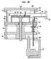
- FIG. 3Ashows a cross-sectional view of a reactor with a shutter in a closed position, in accordance with certain preferred embodiments of the present invention.
- FIG. 3Bshows a cross-sectional view of the reactor of FIG. 3A with the shutter in the open position.
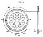
- FIG. 4shows a top view of the reactor of FIG. 3A taken along cross-sectional line IV-IV.
- a reactor 120such as a chemical vapor deposition (CVD) reactor is preferably made of vacuum-grade stainless steel.
- the reactordesirably includes a reaction chamber 122 having a cylindrical wall 124 with an upper end 126 and a lower end 128 remote therefrom.
- Reactor 120desirably includes an injector flange 130 secured over the upper end 126 of cylindrical wall 124 .
- Injector flange 130preferably introduces reactants, such as reactant gases for growing epitaxial layers, into an interior region 132 of the reaction chamber.
- injector flange 130includes a showerhead type water-cooled injector for introducing the reactants inside the reaction chamber 122 .
- a water-cooled element 136may be positioned between an underside 138 of injector flange 130 and cylindrical wall 124 for maintaining the injector flange within a preferred temperature range.
- the injector flange 130is preferably disk shaped and has an outer periphery which substantially conforms to the shape of a circular opening at the top of the cylindrical wall 124 so that when the injector flange 130 is secured to the reaction chamber 122 , the injector flange 130 and reaction chamber form an air-tight seal.
- the CVD reactorpreferably includes a sealing element 125 for forming the air-tight seal between the cylindrical wall 124 and the injector flange 130 .
- the injector flangemay also include a plurality of bores (not shown) adjacent the outer periphery thereof so that fasteners, such as bolts or screws, may be placed through the bores for securing the injector flange to the chamber.
- the injector flangemay remain permanently secured to the chamber.
- the injector flangemay be removable for gaining access to the inside of the reactor.
- Reactor 120may also include an exhaust conduit (not shown) for removing exhaust gases from the inside or interior region 132 of reaction chamber 122 .
- the exhaust conduitmay extend from a bottom portion of the reaction chamber 122 .
- Reactor 120also preferably includes a base plate 142 secured over the lower edge 128 of cylindrical wall 124 .
- Base plate 142is preferably affixed to a lower end of cylindrical wall 124 . As such, base plate 142 is stationary.
- the stationary base plate 142may have a cavity for receiving a cooling fluid for maintaining the base plate at an optimal temperature for growing uniform epitaxial layers.
- Reaction chamber 122preferably includes a passthrough opening 144 extending through cylindrical wall 124 for inserting a wafer carrier into, and removing the wafer carrier from, the interior region 132 of reaction chamber 122 .
- passthrough opening 144preferably includes a flange 146 connectable through a gate valve (not shown) with a loading apparatus for inserting and removing the wafer carriers from the reaction chamber 122 .
- the cylindrical wall 124may include a cooling jacket (not shown) in thermal communication therewith. The cooling jacket preferably receives a coolant therein that serves to maintain the temperature of cylindrical wall 124 within preferred ranges for optimizing formation of uniform epitaxial layers.
- the preferred embodiments of the CVD reactor disclosed hereinmay be used to grow a broad range of epitaxial layers over wafers. These include such Group III-V compound semiconductors as GaAs, GaP, GaAs 1 ⁇ x P x , Ga 1 ⁇ y Al y As, Ga 1 ⁇ y In y As, AlAs, InAs, InP, InGaP, InSb, GaN, InGaN, and the like. However, the CVD reactors disclosed herein may also be utilized to produce other compounds.
- Group II-VI compoundssuch as ZnSe, CdTe, HgCdTe, CdZnTe, CdSeTe, and the like
- Group IV-IV compoundssuch as SiC, diamond, and SiGe
- oxidessuch as YBCO, BaTiO, MgO 2 , ZrO, SiO 2 , ZnO and ZnSiO
- metalssuch as Al, Cu and W.
- the resultant materialswill have a wide range of electronic and opto-electronic applications, including high brightness light emitting diodes (LED's ), lasers, solar cells, photocathodes, HEMT's and MESFET's .
- the reactorincludes a movable, cylindrical shutter 148 .
- Cylindrical shutter 148is preferably movable between open and closed positions for selectively closing passthrough opening 144 .
- passthrough opening 144is substantially closed by substantially cylindrical shutter 148 during an epitaxial layer deposition process.
- Cylindrical shutter 148desirably has an internal cavity 150 .
- reactor 120includes tubing 152 in fluid communication with the internal cavity 150 .
- a cooling fluidpasses through the tubing and into the internal cavity 150 for maintaining the temperature of shutter 148 within desired ranges. As a result, the cooling fluid may be continuously recirculated within the internal cavity 150 so as to maintain a desired cooling temperature for shutter 148 .
- Each tube 152desirably includes an upper end 154 secured to a bottom wall 156 of shutter 148 .
- bottom wall 156 of shutter 148includes openings (not shown) for receiving the upper ends 154 of tubing 152 .
- the upper ends 154 of tubing 152are preferably permanently secured in the openings (not shown) of bottom wall 156 .
- Tubing 152also includes a lower end 158 preferably in fluid communication with a source of cooling fluid, such as a reservoir of water (not shown).
- An intermediate portion 160 of tubing 152 between upper and lower ends 154 , 158extends through an opening 162 of stationary base plate 142 .
- Base plate 142may include a base plate cavity 164 for receiving a cooling fluid.
- An intermediate portion 160 of tubing 152preferably slides freely through the opening 162 of stationary base plate 142 .
- tubingslide freely relative to base plate 142 for moving shutter 148 in an axial direction designated A-A, the axial direction A-A being substantially parallel to the longitudinal axis of tubing 152 .
- Reactor 120also desirably includes a spacer plate 166 attached to an underside 168 of base plate 142 .
- Reactor 120may also include a movable plate 170 under base plate 142 .
- Movable plate 142is movable toward and away from injection flange 130 along axis A-A.
- Movable plate 170desirably has an upper surface 174 , a lower surface 176 , and an opening extending therebetween.
- Tubing 152 for supplying the cooling fluidpreferably extends through the opening 172 of movable plate, however, tubing 152 is secured to movable plate 170 . As a result, tubing 152 and movable plate 170 move simultaneously with one another.
- Reactor 120also has an actuating element 178 having an arm 180 connected to the underside 176 of movable plate 170 .
- Actuating element 178may be actuated for moving the movable plate toward and away from base plate 142 in a direction substantially parallel to the axis designated A-A.
- a flexible bellows structure 182desirably maintains an airtight seal with an underside 168 of base plate 142 . Bellows 182 also allows movable plate 170 and tubing 152 to move relative to base plate 142 .
- Reactor 120includes a linear motion guide 184 extending through a guide opening 186 of movable plate 170 .
- the linear motion guide 184guides movement of movable plate 170 toward and away from base plate 142 in a direction substantially parallel to the axis A-A.
- Reactor 120also includes a base plate 188 mounted atop base member 179 of actuating element 178 .
- Reactor 120also includes a spindle 189 having an upper end 190 located within the interior region 132 of reaction chamber 122 and a lower end 192 located outside reaction chamber 122 .
- spindle 189has an internal cavity adapted to receive a cooling fluid.
- Upper end 190 of spindle 189is sized and shaped to secure wafer carriers 196 thereon.
- the wafer carrier 196may be adapted to hold one or more semiconductor wafers used for growing epitaxial layers thereon.
- Reactor 120also includes radiant heating elements 198 for ensuring uniform temperatures across the top surface of wafer carrier and/or the semiconductor wafers secured thereon.
- Reactor 120may also include heat shields 200 that direct heat from the radiant heating elements toward wafer carrier and wafers stored thereon.
- Reaction chamber 122may also include a second heat shield 202 extending in a direction transverse to first heat shields 200 .
- Second heat shield 202may be cylindrical in shape and may surround the outer perimeter of wafer carrier 196 .
- Reactor 120includes a rotary feedthrough 204 secured to base plate 142 .
- Rotary feedthrough 204may be a ferrofluidic type feedthrough that is operated using an electrical motor (not shown). The rotary feedthrough preferably forms an airtight seal at the interface between rotary feedthrough 204 and base plate 142 so as to maintain a vacuum within the interior region 132 of reaction chamber 122 .
- Shutter 148is movable between a first position ( FIG. 3A ) for closing passthrough opening 144 and a second position ( FIG. 3B ) for opening passthrough opening 144 so as to allow one or more wafer carriers 196 to be inserted into and/or removed from the interior region 132 of reaction chamber 122 .
- shutter 148may be moved from the second open position to the first closed position until an upper end of shutter abuts against an underside of water-cooled element 136 , thereby closing passthrough opening 144 .
- reactantsare introduced through baffle plate 134 of injector flange 130 .
- introducing cooling fluid into the internal cavity 150 of shutter 148provides more responsive control of the temperature of shutter 148 at a desired temperature level so as to minimize thermal discontinuities across the wafer surfaces upon which epitaxial layers are grown.
- temperature discontinuities across the face of a wafermay result in the formation of defective epitaxial layers.
- temperature discontinuitiesmay cause the reactant gases to react prematurely, too late, or at different rates which may change the character of the epitaxial layer or a specific region of the epitaxial layer.
- the cooled shutter 148also preferably provides for uniform flow fields across the top surface of wafer carrier 196 .
- a cylindrical shutterin certain preferred embodiments also minimizes thermal and flow field discontinuities because, inter alia, the shutter completely surrounds the outer perimeter of the wafer carrier which is preferable to a shutter that borders only a portion of the peripheral edge of the wafer carrier.
- shutter 148is moved downward by force transferred from actuating element 178 through movable tubing 152 , and then to shutter 148 . Once shutter 148 has been moved to the second open position shown in FIG. 3B , wafer carrier 196 may be removed from reactor 120 through passthrough opening 144 , and another wafer carrier secured atop spindle 189 .
Landscapes
- Engineering & Computer Science (AREA)
- Chemical & Material Sciences (AREA)
- Manufacturing & Machinery (AREA)
- General Physics & Mathematics (AREA)
- Physics & Mathematics (AREA)
- Computer Hardware Design (AREA)
- Microelectronics & Electronic Packaging (AREA)
- Power Engineering (AREA)
- Condensed Matter Physics & Semiconductors (AREA)
- General Chemical & Material Sciences (AREA)
- Chemical Kinetics & Catalysis (AREA)
- Materials Engineering (AREA)
- Metallurgy (AREA)
- Organic Chemistry (AREA)
- Crystallography & Structural Chemistry (AREA)
- Mechanical Engineering (AREA)
- Chemical Vapour Deposition (AREA)
- Crystals, And After-Treatments Of Crystals (AREA)
Abstract
Description
- The present application is a divisional of U.S. patent application Ser. No. 10/046,426, filed Jan. 16, 2002, now allowed, which claims benefit of U.S. Provisional Application Ser. No. 60/296,598, filed Jun. 7, 2001.
- The present invention relates to reactors for growing epitaxial layers over substrates and more particularly relates to chemical vapor deposition (CVD) reactors designed to minimize thermal and flow field disturbances within the reactor.
- Microelectronic elements, such as semiconductor chips, are frequently manufactured by placing semiconductor wafers within a reaction chamber of a chemical vapor deposition (CVD) reactor and growing epitaxial layers on the wafers. The epitaxial layers are typically grown by causing reactant chemicals in gaseous form to flow over the wafers in controlled quantities and at controlled rates. The wafers are then cut into individual semiconductor chips.
- The reactant chemicals are generally delivered to the reaction chamber by placing the reactant chemicals in a device known as a bubbler and mixing a carrier gas with the reactant chemicals. The bubbler may include adjustable controls for modifying the concentration of the reactant chemicals in the carrier gas. The carrier gas picks up molecules of the reactant chemicals as the gas passes through the bubbler. The reactant gas is then directed into the CVD reactor via a mass flow controller and flow flange.
- There are presently a wide variety of CVD reactors having various designs. These include horizontal reactors wherein a wafer carrier is rotatably mounted inside a reactor and reactant gases are introduced from above the wafer carrier; horizontal reactors with planetary rotation in which the reactant gases pass across a wafer carrier; barrel reactors; and vertical disk reactors in which the reactant gas is injected downwardly onto a substrate surface that is rotating within a reactor. The above described CVD reactors have been successfully used to grow a wide array of epitaxial layers on wafers, including various combinations of semiconductor, thin-film devices and multi-layered structures such as lasers and LED's.
FIG. 1 shows a typical prior art reactor including awafer 10 mounted on awafer carrier 12 which, in turn, is mounted on asusceptor 14. Thesusceptor 14 is mounted on a rotatingsupport spindle 16 for rotating the wafer carrier. Thesusceptor 14,wafer carrier 12 andwafer 10 are typically located insidereactor 18. Aheating assembly 20 is arranged belowsusceptor 14 for heating thesusceptor 14,wafer carrier 12, and wafer10 mounted thereon. During deposition of epitaxial layers,wafer carrier 12 is rotated so as to enhance the temperature uniformity across the deposition area, as well as the flow uniformity of the reactant gases flowing over the deposition area.- Referring to
FIG. 2 ,wafer carriers 12 typically include a plurality ofcylindrical pockets 22 provided on an upper surface thereof for securing the wafers in place as the wafer carrier is rotated. These wafer carriers ordinarily also include anannular flange 24 used for lifting and transporting the wafer carrier into and out of the reaction chamber. During the deposition process, a bottom surface of the wafer carrier may include an annular wall26 for locating the wafer carrier concentrically onrotatable susceptor 14, and for creating agap 28 between the upper surface ofsusceptor 14 and the underside ofwafer carrier 12. The presence ofgap 28 eliminates localized heating of the wafer carrier that may result from direct contact betweenwafer carrier 12 andsusceptor 14, thereby enhancing the uniform transfer of heat fromsusceptor 14 to wafercarrier 12. - As suggested above, the conditions or parameters under which the reactant gases are introduced into the reaction chamber have a dramatic effect upon the quality of the epitaxial layers grown on the wafers. These parameters include material viscosity, density, vapor pressure, the flow path of the reactant gases, chemical activity and/or temperature. In order to optimize the quality of the epitaxial layers, the above-identified parameters are frequently modified, and the effects of such modifications studied. One parameter that is frequently altered during research and development efforts is the flow path of the reactant gases. For example, the specific design of flow nozzles, or the distance between the flow nozzle(s) and a wafer carrier is modified.
- Reactor designers seek to maintain a uniform temperature and flow fields across the surface of each wafer. The ability to maintain uniform temperatures must be repeatable, precise and independent of process conditions. Deviation from a uniform temperature standard by only a few degrees centigrade may result in severe defects in the quality and nature of devices fabricated from the wafers. Moreover, a disturbance in the uniformity of the flow fields may also result in the growth of defective epitaxial layers. For example, the thickness of one or more epitaxially layers may vary across the face of the wafer.
- There have been a number of efforts directed to controlling temperature and flow conditions within a reaction chamber. For example, U.S. Pat. 6,039,811 to Park et al. discloses a reactor for growing epitaxial layers including a gate valve having a cooling jacket attached thereto. The reactor has five cooling jackets: a first cooling jacket on a first sidewall, a second cooling jacket on a second sidewall, a third cooling jacket on an upper wall, a fourth cooling jacket on a lower wall, and a fifth cooling jacket on the gate valve. The reactor includes a wafer transfer chamber having a robot arm for transferring a wafer from a cassette chamber to a reaction chamber. The reactor also includes a wafer cooling chamber for cooling the wafer after the fabricating process is complete. A gate valve, formed on a first sidewall, separates the wafer transfer chamber from the reaction chamber, and a gas injection opening passes through an upper wall of the reactor. A coolant, such as water or a mixture of water and ethylene glycol, is used in the cooling jackets.
- U.S. Pat. 6,086,362 to White et al. discloses a chemical deposition chamber having an opening for transferring substrates into and out of the chamber. The chamber includes a chamber body that is heated by resistive elements secured thereto. The chamber also includes a lid secured to the chamber body. An opening in a sidewall of the chamber body provides a passageway for transferring substrates into and out of the chamber. The chamber also has a gas delivery tube for delivering reactanct gases to the interior of the chamber. As the chamber is heated, cooling water tubes in thermal communication with outer walls of the chamber maintain the temperature of the chamber walls within a desired range so as to prevent the chamber walls from becoming too hot, a condition which may adversely affect the uniformity of epitaxial layers grown on wafers.
- U.S. Pat. Nos. 5,497,727 and 5,942,038 to Mayeda et al. disclose a cooling element for a deposition chamber having an upper vessel and a lower vessel with opposing sealing flanges that extend around the circumference thereof. A cooling assembly is mounted on the sealing flange, and a cooling medium, such as water, is passed through the cooling assembly to reduce the operating temperature of a portion of a resilient sealing member in contact with the sealing flange, thereby extending the useful life of the resilient sealing member.
- U.S. Pat. 4,747,368 to Brien et al. discloses a chemical vapor deposition chamber having a manifold surrounded by cooling tubes. The deposition chamber is adapted to receive wafer substrates that are supported within the chamber and heated to a predetermined reaction temperature. A manifold, disposed within the chamber, has a plurality of openings therein for evenly distributing reactant gases over the wafer substrates for optimizing the growth of epitaxial layers on the substrates. The chamber includes a door for inserting and removing substrates from the reactor, and a sealing ring that enables the formation of an air-tight seal between the door and the chamber. The cooling tubes surround the manifold for maintaining the manifold at an optimal temperature for growing epitaxial layers. The cooling tubes also prevent the reactant gases from reacting prematurely within the manifold.
- In spite of the above improvements, there remains a need for a CVD reactor that minimizes disturbances in the uniformity of thermal and flow fields inside the reactor, thereby resulting in the formation of precise, repeatable and uniform epitaxial layers on wafers.
- In accordance with certain preferred embodiments of the present invention, a reactor for growing epitaxial layers for semiconductor wafers includes a reaction chamber, such as an airtight reaction chamber made of stainless steel. The reactor preferably includes a passthrough opening for inserting and removing wafers and/or wafer carriers from the reaction chamber. The reactor also desirably includes a cylindrical shutter located inside the reaction chamber for selectively closing the passthrough opening. The cylindrical shutter is desirably movable between a first position for closing the passthrough opening and a second position for opening the passthrough opening. The cylindrical shutter desirably includes an internal cavity that is adapted to receive a cooling fluid, such as water. Although the present invention is not limited by any particular theory of operation, it is believed that utilizing a cylindrical shutter that substantially surrounds the wafer carrier will minimize flow field disturbances, thereby resulting in uniform epitaxial layers. Moreover, providing a cooling fluid to the internal cavity of a shutter will minimize thermal discontinuities across the wafer carrier. In certain preferred embodiments, the cooling fluid is a fluid selected from the group consisting of water, oil and any other liquid with a boiling temperature of about 100 degrees Celsius or greater
- The reactor may include tubing in fluid communication with the internal cavity of the shutter for supplying the cooling fluid to the internal cavity. The tubing may include at least one inlet tube for introducing the cooling fluid into the shutter and at least one outlet tube for removing the cooling fluid from the shutter. The inlet and outlet tubes desirably circulate the cooling fluid through the shutter during operation of the reactor. In certain preferred embodiments, the tubing includes two or more inlet tubes for introducing the cooling fluid into the internal cavity of the shutter and two or more outlet tubes for removing the cooling fluid from the internal cavity of the shutter. The tubing is desirably connected to the shutter and moves simultaneously with the shutter as the shutter travels between its first and second positions.
- The reactor also desirably includes an injection flange secured to the reaction chamber for introducing reactant gases inside the reaction chamber. As used herein, the term reactant gases means any gases and vapors existing at conditions prevailing within the reaction chamber, and may include gases introduced into the reaction chamber at elevated temperatures and reduced pressures. The reactant gases may be diluted by mixing another gas therewith, such as an inert gas. The CVD reactor may also include one or more reactant gas injectors for introducing the reactant gas into the interior region of the chamber, such as those disclosed in commonly assigned U.S. patent application Ser. No. 09/146,224, filed Sep. 2, 1998, the disclosure of which is hereby incorporated by reference herein. Each gas injector preferably includes one or more passageways for passing the reactant gas from the exterior region of the chamber, through the apertures in the walls of the chamber, and into the interior region thereof.
- The CVD reactor may include a wafer carrier that is mounted within the interior region of the reaction chamber. The wafer carrier desirably includes a first surface having a growth area for receiving one or more wafers. The first surface of the wafer carrier may have depressions or pockets for receiving the individual wafers. The substrate carrier is preferably mounted for rotation within the interior region of the chamber so that the one or more wafers may be rotated while the reactant gases are introduced into the interior region of the chamber and atop the wafers. In certain embodiments, the substrate carrier is mounted for rotating in a substantially horizontal plane. In other embodiments, the substrate carrier rotates within a substantially vertical plane. In yet further embodiments, the substrate carrier may rotate within any plane lying between horizontal and vertical planes.
- The reactor may also include one or more heating elements in communication with the reaction chamber for heating the wafers and/or wafer carriers secured therein. The heating elements desirably provide a uniform temperature across the top surfaces of the wafers. In certain preferred embodiments, the heating element(s) are provided inside the reaction chamber. The reaction chamber may also have one or more heat shields provided therein, adjacent the one or more heating elements, for directing heat from the heating elements toward the wafers and/or wafer carriers.
- In other preferred embodiments of the present invention, a reactor for growing epitaxial layers on wafers and/or wafer carriers includes a reaction chamber having a passthrough opening for inserting and removing wafer carriers from the reaction chamber, and a cylindrical shutter located inside the reaction chamber for selectively closing the passthrough opening. The cylindrical shutter is desirably movable between a first position for closing the passthrough opening and a second position for opening the passthrough opening. The cylindrical shutter is desirably substantially hollow and includes an internal cavity adapted to receive a cooling fluid. The reactor also desirably includes tubing in fluid communication with the internal cavity of the cylindrical shutter for supplying the cooling fluid to the internal cavity, and a rotatable spindle having an upper end located inside the reaction chamber, with at least one wafer carrier securable to the upper end of the spindle. When the wafer carrier has been secured atop the spindle, the cylindrical shutter preferably surrounds the outer perimeter of the wafer carrier. By completely surrounding the wafer carrier, as opposed to surrounding only a portion of the wafer carrier, flow field and temperature discontinuities are avoided.
- In certain preferred embodiments, the tubing for the cooling fluid has an upper end connected to the shutter and a lower end located outside the reaction chamber and in communication with a reservoir of the cooling fluid. The reactor includes a movable plate having the tubing connected thereto so that the movable plate and tubing move simultaneously together when the shutter is moving between the opened and closed positions. An actuating element is connected to the movable plate for moving the movable plate, the tubing and the shutter between the first position for opening the passthrough opening and the second position for closing the passthrough opening. The tubing desirably slides through openings in the base plate of the reactor. The reactor may also include a guide element in contact with the movable plate for guiding movement of the movable plate along an axial direction substantially parallel to a longitudinal axis of the tubing.
- These and other preferred embodiments will be provided in more detail below.
FIG. 1 shows a cross-sectional view of a prior art reactor including a wafer carrier, susceptor and rotatable spindle.FIG. 2 shows an enlarged view of the wafer carrier, susceptor and rotatable spindle ofFIG. 1 .FIG. 3A shows a cross-sectional view of a reactor with a shutter in a closed position, in accordance with certain preferred embodiments of the present invention.FIG. 3B shows a cross-sectional view of the reactor ofFIG. 3A with the shutter in the open position.FIG. 4 shows a top view of the reactor ofFIG. 3A taken along cross-sectional line IV-IV.- Referring to
FIG. 3A , in accordance with one preferred embodiment of the present invention, areactor 120, such as a chemical vapor deposition (CVD) reactor is preferably made of vacuum-grade stainless steel. The reactor desirably includes areaction chamber 122 having acylindrical wall 124 with anupper end 126 and alower end 128 remote therefrom.Reactor 120 desirably includes aninjector flange 130 secured over theupper end 126 ofcylindrical wall 124.Injector flange 130 preferably introduces reactants, such as reactant gases for growing epitaxial layers, into aninterior region 132 of the reaction chamber. In particular preferred embodiments,injector flange 130 includes a showerhead type water-cooled injector for introducing the reactants inside thereaction chamber 122. A water-cooledelement 136 may be positioned between anunderside 138 ofinjector flange 130 andcylindrical wall 124 for maintaining the injector flange within a preferred temperature range. - The
injector flange 130 is preferably disk shaped and has an outer periphery which substantially conforms to the shape of a circular opening at the top of thecylindrical wall 124 so that when theinjector flange 130 is secured to thereaction chamber 122, theinjector flange 130 and reaction chamber form an air-tight seal. The CVD reactor preferably includes a sealingelement 125 for forming the air-tight seal between thecylindrical wall 124 and theinjector flange 130. The injector flange may also include a plurality of bores (not shown) adjacent the outer periphery thereof so that fasteners, such as bolts or screws, may be placed through the bores for securing the injector flange to the chamber. Once the injector flange has been secured atop the cylindrical wall and an air-tight seal has been formed therebetween, the injector flange may remain permanently secured to the chamber. In other preferred embodiments, the injector flange may be removable for gaining access to the inside of the reactor. Reactor 120 may also include an exhaust conduit (not shown) for removing exhaust gases from the inside orinterior region 132 ofreaction chamber 122. In certain preferred embodiments, the exhaust conduit may extend from a bottom portion of thereaction chamber 122.Reactor 120 also preferably includes abase plate 142 secured over thelower edge 128 ofcylindrical wall 124.Base plate 142 is preferably affixed to a lower end ofcylindrical wall 124. As such,base plate 142 is stationary. Thestationary base plate 142 may have a cavity for receiving a cooling fluid for maintaining the base plate at an optimal temperature for growing uniform epitaxial layers.Reaction chamber 122 preferably includes apassthrough opening 144 extending throughcylindrical wall 124 for inserting a wafer carrier into, and removing the wafer carrier from, theinterior region 132 ofreaction chamber 122. Referring toFIGS. 3A and 4 , passthrough opening144 preferably includes aflange 146 connectable through a gate valve (not shown) with a loading apparatus for inserting and removing the wafer carriers from thereaction chamber 122. Thecylindrical wall 124 may include a cooling jacket (not shown) in thermal communication therewith. The cooling jacket preferably receives a coolant therein that serves to maintain the temperature ofcylindrical wall 124 within preferred ranges for optimizing formation of uniform epitaxial layers.- The preferred embodiments of the CVD reactor disclosed herein may be used to grow a broad range of epitaxial layers over wafers. These include such Group III-V compound semiconductors as GaAs, GaP, GaAs1−xPx, Ga1−yAlyAs, Ga1−yInyAs, AlAs, InAs, InP, InGaP, InSb, GaN, InGaN, and the like. However, the CVD reactors disclosed herein may also be utilized to produce other compounds. These include Group II-VI compounds, such as ZnSe, CdTe, HgCdTe, CdZnTe, CdSeTe, and the like; Group IV-IV compounds, such as SiC, diamond, and SiGe; as well as oxides, such as YBCO, BaTiO, MgO2, ZrO, SiO2, ZnO and ZnSiO; and metals, such as Al, Cu and W. Furthermore, the resultant materials will have a wide range of electronic and opto-electronic applications, including high brightness light emitting diodes (LED's ), lasers, solar cells, photocathodes, HEMT's and MESFET's .
- Referring to
FIGS. 3A and 3B , the reactor includes a movable,cylindrical shutter 148.Cylindrical shutter 148 is preferably movable between open and closed positions for selectively closingpassthrough opening 144. As shown inFIG. 3A ,passthrough opening 144 is substantially closed by substantiallycylindrical shutter 148 during an epitaxial layer deposition process.Cylindrical shutter 148 desirably has aninternal cavity 150. andreactor 120 includestubing 152 in fluid communication with theinternal cavity 150. A cooling fluid passes through the tubing and into theinternal cavity 150 for maintaining the temperature ofshutter 148 within desired ranges. As a result, the cooling fluid may be continuously recirculated within theinternal cavity 150 so as to maintain a desired cooling temperature forshutter 148. Eachtube 152 desirably includes anupper end 154 secured to abottom wall 156 ofshutter 148. In specific preferred embodiments,bottom wall 156 ofshutter 148 includes openings (not shown) for receiving the upper ends154 oftubing 152. The upper ends154 oftubing 152 are preferably permanently secured in the openings (not shown) ofbottom wall 156.Tubing 152 also includes alower end 158 preferably in fluid communication with a source of cooling fluid, such as a reservoir of water (not shown). Anintermediate portion 160 oftubing 152 between upper and lower ends154,158 extends through anopening 162 ofstationary base plate 142.Base plate 142 may include abase plate cavity 164 for receiving a cooling fluid. Anintermediate portion 160 oftubing 152 preferably slides freely through theopening 162 ofstationary base plate 142. As will be described in more detail below, it is particularly preferred that tubing slide freely relative tobase plate 142 for movingshutter 148 in an axial direction designated A-A, the axial direction A-A being substantially parallel to the longitudinal axis oftubing 152.Reactor 120 also desirably includes aspacer plate 166 attached to anunderside 168 ofbase plate 142. Reactor 120 may also include amovable plate 170 underbase plate 142.Movable plate 142 is movable toward and away frominjection flange 130 along axis A-A.Movable plate 170 desirably has anupper surface 174, alower surface 176, and an opening extending therebetween.Tubing 152 for supplying the cooling fluid preferably extends through theopening 172 of movable plate, however,tubing 152 is secured tomovable plate 170. As a result,tubing 152 andmovable plate 170 move simultaneously with one another.Reactor 120 also has anactuating element 178 having anarm 180 connected to theunderside 176 ofmovable plate 170. Actuatingelement 178 may be actuated for moving the movable plate toward and away frombase plate 142 in a direction substantially parallel to the axis designated A-A. Aflexible bellows structure 182 desirably maintains an airtight seal with anunderside 168 ofbase plate 142.Bellows 182 also allowsmovable plate 170 andtubing 152 to move relative tobase plate 142.Reactor 120 includes alinear motion guide 184 extending through aguide opening 186 ofmovable plate 170. Thelinear motion guide 184 guides movement ofmovable plate 170 toward and away frombase plate 142 in a direction substantially parallel to the axis A-A.Reactor 120 also includes abase plate 188 mounted atopbase member 179 ofactuating element 178.Reactor 120 also includes aspindle 189 having anupper end 190 located within theinterior region 132 ofreaction chamber 122 and alower end 192 located outsidereaction chamber 122. In certain preferred embodiments,spindle 189 has an internal cavity adapted to receive a cooling fluid.Upper end 190 ofspindle 189 is sized and shaped to securewafer carriers 196 thereon. Thewafer carrier 196 may be adapted to hold one or more semiconductor wafers used for growing epitaxial layers thereon.Reactor 120 also includesradiant heating elements 198 for ensuring uniform temperatures across the top surface of wafer carrier and/or the semiconductor wafers secured thereon.Reactor 120 may also includeheat shields 200 that direct heat from the radiant heating elements toward wafer carrier and wafers stored thereon. In the particular embodiment shown inFIG. 3A ,radiant heating elements 198 andheat shields 200 extend in directions substantially parallel to one another.Reaction chamber 122 may also include asecond heat shield 202 extending in a direction transverse tofirst heat shields 200.Second heat shield 202 may be cylindrical in shape and may surround the outer perimeter ofwafer carrier 196.Reactor 120 includes arotary feedthrough 204 secured tobase plate 142.Rotary feedthrough 204 may be a ferrofluidic type feedthrough that is operated using an electrical motor (not shown). The rotary feedthrough preferably forms an airtight seal at the interface betweenrotary feedthrough 204 andbase plate 142 so as to maintain a vacuum within theinterior region 132 ofreaction chamber 122.Shutter 148 is movable between a first position (FIG. 3A ) for closingpassthrough opening 144 and a second position (FIG. 3B ) for openingpassthrough opening 144 so as to allow one ormore wafer carriers 196 to be inserted into and/or removed from theinterior region 132 ofreaction chamber 122. After a wafer carrier has been placed atopspindle 189,shutter 148 may be moved from the second open position to the first closed position until an upper end of shutter abuts against an underside of water-cooledelement 136, thereby closingpassthrough opening 144. Onceshutter 148 has been closed, reactants (not shown) are introduced throughbaffle plate 134 ofinjector flange 130.- Although the present invention is not limited by any particular theory of operation, it is believed that introducing cooling fluid into the
internal cavity 150 ofshutter 148 provides more responsive control of the temperature ofshutter 148 at a desired temperature level so as to minimize thermal discontinuities across the wafer surfaces upon which epitaxial layers are grown. As is known to those skilled in the art, temperature discontinuities across the face of a wafer may result in the formation of defective epitaxial layers. For example, temperature discontinuities may cause the reactant gases to react prematurely, too late, or at different rates which may change the character of the epitaxial layer or a specific region of the epitaxial layer. The cooledshutter 148 also preferably provides for uniform flow fields across the top surface ofwafer carrier 196. - The use of a cylindrical shutter in certain preferred embodiments also minimizes thermal and flow field discontinuities because, inter alia, the shutter completely surrounds the outer perimeter of the wafer carrier which is preferable to a shutter that borders only a portion of the peripheral edge of the wafer carrier.
- The provision of uniform temperature and flow fields results in the formation of uniform epitaxial layers on wafers. When a deposition run is finished,
shutter 148 is moved downward by force transferred from actuatingelement 178 throughmovable tubing 152, and then to shutter148. Onceshutter 148 has been moved to the second open position shown inFIG. 3B ,wafer carrier 196 may be removed fromreactor 120 through passthrough opening144, and another wafer carrier secured atopspindle 189. - As will be appreciated, numerous variations and combinations of the features discussed above may be utilized without departing from the present invention as further defined by the claims. Accordingly, the foregoing description of the preferred embodiments merely illustrates certain aspects of the present invention and in no way limits the scope of the invention
Claims (7)
Priority Applications (1)
| Application Number | Priority Date | Filing Date | Title |
|---|---|---|---|
| US11/129,548US7276124B2 (en) | 2001-06-07 | 2005-05-13 | Reactor having a movable shutter |
Applications Claiming Priority (3)
| Application Number | Priority Date | Filing Date | Title |
|---|---|---|---|
| US29659801P | 2001-06-07 | 2001-06-07 | |
| US10/046,426US6902623B2 (en) | 2001-06-07 | 2002-01-16 | Reactor having a movable shutter |
| US11/129,548US7276124B2 (en) | 2001-06-07 | 2005-05-13 | Reactor having a movable shutter |
Related Parent Applications (1)
| Application Number | Title | Priority Date | Filing Date |
|---|---|---|---|
| US10/046,426DivisionUS6902623B2 (en) | 2001-06-07 | 2002-01-16 | Reactor having a movable shutter |
Publications (2)
| Publication Number | Publication Date |
|---|---|
| US20050217578A1true US20050217578A1 (en) | 2005-10-06 |
| US7276124B2 US7276124B2 (en) | 2007-10-02 |
Family
ID=26723902
Family Applications (2)
| Application Number | Title | Priority Date | Filing Date |
|---|---|---|---|
| US10/046,426Expired - LifetimeUS6902623B2 (en) | 2001-06-07 | 2002-01-16 | Reactor having a movable shutter |
| US11/129,548Expired - LifetimeUS7276124B2 (en) | 2001-06-07 | 2005-05-13 | Reactor having a movable shutter |
Family Applications Before (1)
| Application Number | Title | Priority Date | Filing Date |
|---|---|---|---|
| US10/046,426Expired - LifetimeUS6902623B2 (en) | 2001-06-07 | 2002-01-16 | Reactor having a movable shutter |
Country Status (6)
| Country | Link |
|---|---|
| US (2) | US6902623B2 (en) |
| EP (1) | EP1393359A4 (en) |
| JP (1) | JP2004529272A (en) |
| KR (1) | KR20030018074A (en) |
| CN (1) | CN1265432C (en) |
| WO (1) | WO2002099861A1 (en) |
Cited By (10)
| Publication number | Priority date | Publication date | Assignee | Title |
|---|---|---|---|---|
| US20050051102A1 (en)* | 2003-09-10 | 2005-03-10 | Dainippon Screen Mfg. Co., Ltd. | Apparatus for processing substrate in chamber and maintenance method therefor |
| US20070051312A1 (en)* | 2003-08-07 | 2007-03-08 | Ofer Sneh | Perimeter partition-valve with protected seals and associated small size process chambers and multiple chamber systems |
| US20070281106A1 (en)* | 2006-05-30 | 2007-12-06 | Applied Materials, Inc. | Process chamber for dielectric gapfill |
| US20090120464A1 (en)* | 2007-11-08 | 2009-05-14 | Applied Materials, Inc. | Multi-port pumping system for substrate processing chambers |
| US20090120368A1 (en)* | 2007-11-08 | 2009-05-14 | Applied Materials, Inc. | Rotating temperature controlled substrate pedestal for film uniformity |
| US8889566B2 (en) | 2012-09-11 | 2014-11-18 | Applied Materials, Inc. | Low cost flowable dielectric films |
| US9018108B2 (en) | 2013-01-25 | 2015-04-28 | Applied Materials, Inc. | Low shrinkage dielectric films |
| US9144147B2 (en) | 2011-01-18 | 2015-09-22 | Applied Materials, Inc. | Semiconductor processing system and methods using capacitively coupled plasma |
| US9412581B2 (en) | 2014-07-16 | 2016-08-09 | Applied Materials, Inc. | Low-K dielectric gapfill by flowable deposition |
| US12009228B2 (en) | 2015-02-03 | 2024-06-11 | Applied Materials, Inc. | Low temperature chuck for plasma processing systems |
Families Citing this family (64)
| Publication number | Priority date | Publication date | Assignee | Title |
|---|---|---|---|---|
| WO2003062490A2 (en)* | 2002-01-17 | 2003-07-31 | Sundew Technologies, Llc | Ald apparatus and method |
| JP3887291B2 (en)* | 2002-09-24 | 2007-02-28 | 東京エレクトロン株式会社 | Substrate processing equipment |
| AU2003265542A1 (en) | 2003-08-20 | 2005-03-10 | Veeco Instruments Inc. | Alkyl push flow for vertical flow rotating disk reactors |
| US7780821B2 (en)* | 2004-08-02 | 2010-08-24 | Seagate Technology Llc | Multi-chamber processing with simultaneous workpiece transport and gas delivery |
| JP4707139B2 (en)* | 2005-06-28 | 2011-06-22 | 芝浦メカトロニクス株式会社 | Decompression treatment apparatus and decompression treatment method |
| JP5252850B2 (en)* | 2007-07-30 | 2013-07-31 | 株式会社日立国際電気 | Substrate processing apparatus and semiconductor device manufacturing method |
| US7841475B2 (en)* | 2007-08-15 | 2010-11-30 | Kalustyan Corporation | Continuously operating machine having magnets |
| EP2215282B1 (en) | 2007-10-11 | 2016-11-30 | Valence Process Equipment, Inc. | Chemical vapor deposition reactor |
| TWI397113B (en)* | 2008-08-29 | 2013-05-21 | Veeco Instr Inc | Wafer carrier with varying thermal resistance |
| US8895107B2 (en)* | 2008-11-06 | 2014-11-25 | Veeco Instruments Inc. | Chemical vapor deposition with elevated temperature gas injection |
| CN101994097B (en)* | 2009-08-25 | 2013-08-21 | 鸿富锦精密工业(深圳)有限公司 | Film coating device |
| SG183432A1 (en) | 2010-02-24 | 2012-09-27 | Veeco Instr Inc | Processing methods and apparatus with temperature distribution control |
| SG183511A1 (en) | 2010-03-03 | 2012-09-27 | Veeco Instr Inc | Wafer carrier with sloped edge |
| CN101876055B (en)* | 2010-03-23 | 2012-02-15 | 东莞宏威数码机械有限公司 | Baffle cooling device |
| US8460466B2 (en) | 2010-08-02 | 2013-06-11 | Veeco Instruments Inc. | Exhaust for CVD reactor |
| CN102477546A (en)* | 2010-11-25 | 2012-05-30 | 绿种子能源科技股份有限公司 | Film deposition device with cooling module |
| US8888360B2 (en) | 2010-12-30 | 2014-11-18 | Veeco Instruments Inc. | Methods and systems for in-situ pyrometer calibration |
| US10167554B2 (en) | 2010-12-30 | 2019-01-01 | Veeco Instruments Inc. | Wafer processing with carrier extension |
| KR101553458B1 (en) | 2011-05-19 | 2015-09-15 | 후루카와 기카이 긴조쿠 가부시키가이샤 | Method for washing semiconductor manufacturing apparatus component, apparatus for washing semiconductor manufacturing apparatus component, and vapor phase growth apparatus |
| WO2012166770A2 (en) | 2011-05-31 | 2012-12-06 | Veeco Instruments Inc. | Heated wafer carrier profiling |
| TWI511223B (en) | 2011-06-03 | 2015-12-01 | Hermes Epitek Corp | Semiconductor equipment |
| US9816184B2 (en) | 2012-03-20 | 2017-11-14 | Veeco Instruments Inc. | Keyed wafer carrier |
| CN102618845B (en)* | 2012-04-01 | 2014-06-11 | 中微半导体设备(上海)有限公司 | Reactor with baffle plate device |
| US10316412B2 (en) | 2012-04-18 | 2019-06-11 | Veeco Instruments Inc. | Wafter carrier for chemical vapor deposition systems |
| US9200965B2 (en) | 2012-06-26 | 2015-12-01 | Veeco Instruments Inc. | Temperature control for GaN based materials |
| US20150345046A1 (en)* | 2012-12-27 | 2015-12-03 | Showa Denko K.K. | Film-forming device |
| US20160194753A1 (en)* | 2012-12-27 | 2016-07-07 | Showa Denko K.K. | SiC-FILM FORMATION DEVICE AND METHOD FOR PRODUCING SiC FILM |
| US9388493B2 (en) | 2013-01-08 | 2016-07-12 | Veeco Instruments Inc. | Self-cleaning shutter for CVD reactor |
| US9273413B2 (en) | 2013-03-14 | 2016-03-01 | Veeco Instruments Inc. | Wafer carrier with temperature distribution control |
| US10167571B2 (en) | 2013-03-15 | 2019-01-01 | Veeco Instruments Inc. | Wafer carrier having provisions for improving heating uniformity in chemical vapor deposition systems |
| TWI650832B (en) | 2013-12-26 | 2019-02-11 | 維克儀器公司 | Wafer carrier having thermal cover for chemical vapor deposition systems |
| EP3100298B1 (en) | 2014-01-27 | 2020-07-15 | Veeco Instruments Inc. | Wafer carrier having retention pockets with compound radii for chemical vapor deposition systems |
| US9831754B2 (en) | 2014-03-13 | 2017-11-28 | The Regents Of The University Of Michigan | Miniature mechanical shutter |
| JP6195803B2 (en)* | 2014-05-02 | 2017-09-13 | 東京エレクトロン株式会社 | Substrate processing apparatus, substrate processing method, and storage medium |
| JP6541374B2 (en)* | 2014-07-24 | 2019-07-10 | 東京エレクトロン株式会社 | Substrate processing equipment |
| CN105463407B (en)* | 2014-09-05 | 2018-12-07 | 沈阳拓荆科技有限公司 | Atomic layer deposition apparatus |
| KR101722915B1 (en)* | 2014-10-13 | 2017-04-04 | 주식회사 테스 | Apparatus for mocvd |
| USD793971S1 (en) | 2015-03-27 | 2017-08-08 | Veeco Instruments Inc. | Wafer carrier with a 14-pocket configuration |
| USD793972S1 (en) | 2015-03-27 | 2017-08-08 | Veeco Instruments Inc. | Wafer carrier with a 31-pocket configuration |
| USD778247S1 (en)* | 2015-04-16 | 2017-02-07 | Veeco Instruments Inc. | Wafer carrier with a multi-pocket configuration |
| US9627239B2 (en) | 2015-05-29 | 2017-04-18 | Veeco Instruments Inc. | Wafer surface 3-D topography mapping based on in-situ tilt measurements in chemical vapor deposition systems |
| CN107735857B (en)* | 2015-06-05 | 2022-01-11 | 应用材料公司 | Base positioning and rotating equipment and using method |
| JP6582676B2 (en)* | 2015-07-24 | 2019-10-02 | 東京エレクトロン株式会社 | Load lock device and substrate processing system |
| US9748113B2 (en) | 2015-07-30 | 2017-08-29 | Veeco Intruments Inc. | Method and apparatus for controlled dopant incorporation and activation in a chemical vapor deposition system |
| DE202016104588U1 (en) | 2015-09-03 | 2016-11-30 | Veeco Instruments Inc. | Multi-chamber system for chemical vapor deposition |
| US10954594B2 (en)* | 2015-09-30 | 2021-03-23 | Applied Materials, Inc. | High temperature vapor delivery system and method |
| CN106801222B (en)* | 2015-11-26 | 2018-06-19 | 中晟光电设备(上海)股份有限公司 | A kind of chip tray and MOCVD systems |
| US10571430B2 (en) | 2016-03-14 | 2020-02-25 | Veeco Instruments Inc. | Gas concentration sensors and systems |
| CN105862011B (en)* | 2016-06-14 | 2018-08-24 | 武汉工程大学 | A kind of chemical vapor depsotition equipment special baffle device |
| KR20190001371U (en) | 2017-11-30 | 2019-06-10 | 비코 인스트루먼츠 인코포레이티드 | Wafer carrier with a 33-pocket configuration |
| USD860146S1 (en) | 2017-11-30 | 2019-09-17 | Veeco Instruments Inc. | Wafer carrier with a 33-pocket configuration |
| USD858469S1 (en) | 2018-03-26 | 2019-09-03 | Veeco Instruments Inc. | Chemical vapor deposition wafer carrier with thermal cover |
| USD854506S1 (en) | 2018-03-26 | 2019-07-23 | Veeco Instruments Inc. | Chemical vapor deposition wafer carrier with thermal cover |
| USD863239S1 (en) | 2018-03-26 | 2019-10-15 | Veeco Instruments Inc. | Chemical vapor deposition wafer carrier with thermal cover |
| USD860147S1 (en) | 2018-03-26 | 2019-09-17 | Veeco Instruments Inc. | Chemical vapor deposition wafer carrier with thermal cover |
| USD866491S1 (en) | 2018-03-26 | 2019-11-12 | Veeco Instruments Inc. | Chemical vapor deposition wafer carrier with thermal cover |
| JP7066512B2 (en)* | 2018-05-11 | 2022-05-13 | 東京エレクトロン株式会社 | Plasma processing equipment |
| JP7374016B2 (en)* | 2019-06-18 | 2023-11-06 | 東京エレクトロン株式会社 | Substrate processing equipment |
| CN112251732B (en)* | 2020-08-31 | 2023-02-17 | 广东鼎泰机器人科技有限公司 | Material carrying device of coating machine |
| CN112144112B (en)* | 2020-09-22 | 2022-07-22 | 北京北方华创微电子装备有限公司 | Semiconductor process equipment |
| JP7519874B2 (en)* | 2020-10-27 | 2024-07-22 | 東京エレクトロン株式会社 | Plasma Processing Equipment |
| CN114657643B (en)* | 2020-12-24 | 2023-10-03 | 中国科学院微电子研究所 | Wafer processing apparatus |
| CN113981416B (en)* | 2021-12-29 | 2022-03-22 | 上海陛通半导体能源科技股份有限公司 | Multifunctional wafer pretreatment cavity and chemical vapor deposition equipment |
| WO2023128565A1 (en)* | 2021-12-30 | 2023-07-06 | 주식회사 비아트론 | Epitaxial process semiconductor manufacturing device |
Citations (28)
| Publication number | Priority date | Publication date | Assignee | Title |
|---|---|---|---|---|
| US3656454A (en)* | 1970-11-23 | 1972-04-18 | Air Reduction | Vacuum coating apparatus |
| US4309961A (en)* | 1979-03-29 | 1982-01-12 | Tel-Thermco Engineering Co., Ltd. | Apparatus for thermal treatment of semiconductors |
| US4318889A (en)* | 1980-05-28 | 1982-03-09 | Siemens Aktiengesellschaft | Impermeable cooled closing plug for processing tubes, in particular in semiconductor manufacture |
| US4539933A (en)* | 1983-08-31 | 1985-09-10 | Anicon, Inc. | Chemical vapor deposition apparatus |
| US4565157A (en)* | 1983-03-29 | 1986-01-21 | Genus, Inc. | Method and apparatus for deposition of tungsten silicides |
| US4658513A (en)* | 1985-09-03 | 1987-04-21 | Dynapert-Htc Corporation | Continuous vapor phase processing machine |
| US4690098A (en)* | 1984-06-08 | 1987-09-01 | Atomika Technische Physik Gmbh | Vacuum vapor-deposition system |
| US4747368A (en)* | 1985-05-17 | 1988-05-31 | Mitel Corp. | Chemical vapor deposition apparatus with manifold enveloped by cooling means |
| US5046909A (en)* | 1989-06-29 | 1991-09-10 | Applied Materials, Inc. | Method and apparatus for handling semiconductor wafers |
| US5346513A (en)* | 1991-05-13 | 1994-09-13 | Mitsubishi Denki Kabushiki Kaisha | Method for producing semiconductor device using a vacuum sealing mechanism having inner and outer bellows |
| US5368648A (en)* | 1991-02-26 | 1994-11-29 | Tokyo Electron Sagami Kabushiki Kaisha | Sealing apparatus |
| US5407485A (en)* | 1993-04-09 | 1995-04-18 | F. T. L. Co., Ltd. | Apparatus for producing semiconductor device and method for producing semiconductor device |
| US5497727A (en)* | 1993-09-07 | 1996-03-12 | Lsi Logic Corporation | Cooling element for a semiconductor fabrication chamber |
| US5520742A (en)* | 1993-03-03 | 1996-05-28 | Tokyo Electron Kabushiki Kaisha | Thermal processing apparatus with heat shielding member |
| US5624499A (en)* | 1995-04-28 | 1997-04-29 | Anelva Corporation | CVD apparatus |
| US5788799A (en)* | 1996-06-11 | 1998-08-04 | Applied Materials, Inc. | Apparatus and method for cleaning of semiconductor process chamber surfaces |
| US5854468A (en)* | 1996-01-25 | 1998-12-29 | Brooks Automation, Inc. | Substrate heating apparatus with cantilevered lifting arm |
| US5855677A (en)* | 1994-09-30 | 1999-01-05 | Applied Materials, Inc. | Method and apparatus for controlling the temperature of reaction chamber walls |
| US6001183A (en)* | 1996-06-10 | 1999-12-14 | Emcore Corporation | Wafer carriers for epitaxial growth processes |
| US6039811A (en)* | 1996-06-08 | 2000-03-21 | Samsung Electronics Co., Ltd. | Apparatus for fabricating polysilicon film for semiconductor device |
| US6086362A (en)* | 1998-05-20 | 2000-07-11 | Applied Komatsu Technology, Inc. | Multi-function chamber for a substrate processing system |
| US6111225A (en)* | 1996-02-23 | 2000-08-29 | Tokyo Electron Limited | Wafer processing apparatus with a processing vessel, upper and lower separately sealed heating vessels, and means for maintaining the vessels at predetermined pressures |
| US6192827B1 (en)* | 1998-07-03 | 2001-02-27 | Applied Materials, Inc. | Double slit-valve doors for plasma processing |
| US6340501B1 (en)* | 1997-05-08 | 2002-01-22 | Matsushita Electric Industrial Co., Ltd. | Device and method for manufacturing an optical recording medium |
| US20020069970A1 (en)* | 2000-03-07 | 2002-06-13 | Applied Materials, Inc. | Temperature controlled semiconductor processing chamber liner |
| US20020076490A1 (en)* | 2000-12-15 | 2002-06-20 | Chiang Tony P. | Variable gas conductance control for a process chamber |
| US20020108571A1 (en)* | 1997-03-17 | 2002-08-15 | Russell Black | Heated and cooled vacuum chamber shield |
| US6442950B1 (en)* | 2001-05-23 | 2002-09-03 | Macronix International Co., Ltd. | Cooling system of chamber with removable liner |
Family Cites Families (3)
| Publication number | Priority date | Publication date | Assignee | Title |
|---|---|---|---|---|
| JPH04157162A (en) | 1990-10-22 | 1992-05-29 | Shinko Electric Co Ltd | Surface treating device |
| JPH0770730A (en)* | 1993-09-06 | 1995-03-14 | Hitachi Metals Ltd | Pitting corrosion resistant stainless steel |
| JPH09134880A (en) | 1995-11-09 | 1997-05-20 | Fujitsu Ltd | Semiconductor device manufacturing equipment |
- 2002
- 2002-01-16USUS10/046,426patent/US6902623B2/ennot_activeExpired - Lifetime
- 2002-06-07CNCNB02802611XApatent/CN1265432C/ennot_activeExpired - Fee Related
- 2002-06-07JPJP2003502873Apatent/JP2004529272A/enactivePending
- 2002-06-07EPEP02744280Apatent/EP1393359A4/ennot_activeWithdrawn
- 2002-06-07WOPCT/US2002/018440patent/WO2002099861A1/enactiveApplication Filing
- 2002-06-07KRKR10-2003-7001799Apatent/KR20030018074A/ennot_activeCeased
- 2005
- 2005-05-13USUS11/129,548patent/US7276124B2/ennot_activeExpired - Lifetime
Patent Citations (29)
| Publication number | Priority date | Publication date | Assignee | Title |
|---|---|---|---|---|
| US3656454A (en)* | 1970-11-23 | 1972-04-18 | Air Reduction | Vacuum coating apparatus |
| US4309961A (en)* | 1979-03-29 | 1982-01-12 | Tel-Thermco Engineering Co., Ltd. | Apparatus for thermal treatment of semiconductors |
| US4318889A (en)* | 1980-05-28 | 1982-03-09 | Siemens Aktiengesellschaft | Impermeable cooled closing plug for processing tubes, in particular in semiconductor manufacture |
| US4565157A (en)* | 1983-03-29 | 1986-01-21 | Genus, Inc. | Method and apparatus for deposition of tungsten silicides |
| US4539933A (en)* | 1983-08-31 | 1985-09-10 | Anicon, Inc. | Chemical vapor deposition apparatus |
| US4690098A (en)* | 1984-06-08 | 1987-09-01 | Atomika Technische Physik Gmbh | Vacuum vapor-deposition system |
| US4747368A (en)* | 1985-05-17 | 1988-05-31 | Mitel Corp. | Chemical vapor deposition apparatus with manifold enveloped by cooling means |
| US4658513A (en)* | 1985-09-03 | 1987-04-21 | Dynapert-Htc Corporation | Continuous vapor phase processing machine |
| US5046909A (en)* | 1989-06-29 | 1991-09-10 | Applied Materials, Inc. | Method and apparatus for handling semiconductor wafers |
| US5368648A (en)* | 1991-02-26 | 1994-11-29 | Tokyo Electron Sagami Kabushiki Kaisha | Sealing apparatus |
| US5346513A (en)* | 1991-05-13 | 1994-09-13 | Mitsubishi Denki Kabushiki Kaisha | Method for producing semiconductor device using a vacuum sealing mechanism having inner and outer bellows |
| US5520742A (en)* | 1993-03-03 | 1996-05-28 | Tokyo Electron Kabushiki Kaisha | Thermal processing apparatus with heat shielding member |
| US5407485A (en)* | 1993-04-09 | 1995-04-18 | F. T. L. Co., Ltd. | Apparatus for producing semiconductor device and method for producing semiconductor device |
| US5497727A (en)* | 1993-09-07 | 1996-03-12 | Lsi Logic Corporation | Cooling element for a semiconductor fabrication chamber |
| US5942038A (en)* | 1993-09-07 | 1999-08-24 | Lsi Logic Corporation | Cooling element for a semiconductor fabrication chamber |
| US5855677A (en)* | 1994-09-30 | 1999-01-05 | Applied Materials, Inc. | Method and apparatus for controlling the temperature of reaction chamber walls |
| US5624499A (en)* | 1995-04-28 | 1997-04-29 | Anelva Corporation | CVD apparatus |
| US5854468A (en)* | 1996-01-25 | 1998-12-29 | Brooks Automation, Inc. | Substrate heating apparatus with cantilevered lifting arm |
| US6111225A (en)* | 1996-02-23 | 2000-08-29 | Tokyo Electron Limited | Wafer processing apparatus with a processing vessel, upper and lower separately sealed heating vessels, and means for maintaining the vessels at predetermined pressures |
| US6039811A (en)* | 1996-06-08 | 2000-03-21 | Samsung Electronics Co., Ltd. | Apparatus for fabricating polysilicon film for semiconductor device |
| US6001183A (en)* | 1996-06-10 | 1999-12-14 | Emcore Corporation | Wafer carriers for epitaxial growth processes |
| US5788799A (en)* | 1996-06-11 | 1998-08-04 | Applied Materials, Inc. | Apparatus and method for cleaning of semiconductor process chamber surfaces |
| US20020108571A1 (en)* | 1997-03-17 | 2002-08-15 | Russell Black | Heated and cooled vacuum chamber shield |
| US6340501B1 (en)* | 1997-05-08 | 2002-01-22 | Matsushita Electric Industrial Co., Ltd. | Device and method for manufacturing an optical recording medium |
| US6086362A (en)* | 1998-05-20 | 2000-07-11 | Applied Komatsu Technology, Inc. | Multi-function chamber for a substrate processing system |
| US6192827B1 (en)* | 1998-07-03 | 2001-02-27 | Applied Materials, Inc. | Double slit-valve doors for plasma processing |
| US20020069970A1 (en)* | 2000-03-07 | 2002-06-13 | Applied Materials, Inc. | Temperature controlled semiconductor processing chamber liner |
| US20020076490A1 (en)* | 2000-12-15 | 2002-06-20 | Chiang Tony P. | Variable gas conductance control for a process chamber |
| US6442950B1 (en)* | 2001-05-23 | 2002-09-03 | Macronix International Co., Ltd. | Cooling system of chamber with removable liner |
Cited By (14)
| Publication number | Priority date | Publication date | Assignee | Title |
|---|---|---|---|---|
| US20100166957A1 (en)* | 2003-08-07 | 2010-07-01 | Sundew Technologies, Llc | Perimeter partition-valve with protected seals and associated small size process chambers and multiple chamber systems |
| US20070051312A1 (en)* | 2003-08-07 | 2007-03-08 | Ofer Sneh | Perimeter partition-valve with protected seals and associated small size process chambers and multiple chamber systems |
| US8252116B2 (en)* | 2003-08-07 | 2012-08-28 | Sundew Technologies, Llc | Perimeter partition-valve with protected seals and associated small size process chambers and multiple chamber systems |
| US7682454B2 (en)* | 2003-08-07 | 2010-03-23 | Sundew Technologies, Llc | Perimeter partition-valve with protected seals and associated small size process chambers and multiple chamber systems |
| US20050051102A1 (en)* | 2003-09-10 | 2005-03-10 | Dainippon Screen Mfg. Co., Ltd. | Apparatus for processing substrate in chamber and maintenance method therefor |
| US20070281106A1 (en)* | 2006-05-30 | 2007-12-06 | Applied Materials, Inc. | Process chamber for dielectric gapfill |
| US20090120464A1 (en)* | 2007-11-08 | 2009-05-14 | Applied Materials, Inc. | Multi-port pumping system for substrate processing chambers |
| US7964040B2 (en) | 2007-11-08 | 2011-06-21 | Applied Materials, Inc. | Multi-port pumping system for substrate processing chambers |
| US20090120368A1 (en)* | 2007-11-08 | 2009-05-14 | Applied Materials, Inc. | Rotating temperature controlled substrate pedestal for film uniformity |
| US9144147B2 (en) | 2011-01-18 | 2015-09-22 | Applied Materials, Inc. | Semiconductor processing system and methods using capacitively coupled plasma |
| US8889566B2 (en) | 2012-09-11 | 2014-11-18 | Applied Materials, Inc. | Low cost flowable dielectric films |
| US9018108B2 (en) | 2013-01-25 | 2015-04-28 | Applied Materials, Inc. | Low shrinkage dielectric films |
| US9412581B2 (en) | 2014-07-16 | 2016-08-09 | Applied Materials, Inc. | Low-K dielectric gapfill by flowable deposition |
| US12009228B2 (en) | 2015-02-03 | 2024-06-11 | Applied Materials, Inc. | Low temperature chuck for plasma processing systems |
Also Published As
| Publication number | Publication date |
|---|---|
| US20020185068A1 (en) | 2002-12-12 |
| EP1393359A1 (en) | 2004-03-03 |
| CN1265432C (en) | 2006-07-19 |
| US7276124B2 (en) | 2007-10-02 |
| US6902623B2 (en) | 2005-06-07 |
| EP1393359A4 (en) | 2006-11-22 |
| WO2002099861A1 (en) | 2002-12-12 |
| KR20030018074A (en) | 2003-03-04 |
| CN1465094A (en) | 2003-12-31 |
| JP2004529272A (en) | 2004-09-24 |
Similar Documents
| Publication | Publication Date | Title |
|---|---|---|
| US7276124B2 (en) | Reactor having a movable shutter | |
| US4649859A (en) | Reactor design for uniform chemical vapor deposition-grown films without substrate rotation | |
| JP3252960B2 (en) | Semiconductor thin film deposition equipment for atomic layer epitaxy process | |
| KR100415475B1 (en) | Apparatus for growing thin films onto a substrate | |
| US6214116B1 (en) | Horizontal reactor for compound semiconductor growth | |
| KR101855217B1 (en) | Wafer processing with carrier extension | |
| US8092599B2 (en) | Movable injectors in rotating disc gas reactors | |
| EP0972092B1 (en) | Multipurpose processing chamber for chemical vapor deposition processes | |
| US6080241A (en) | Chemical vapor deposition chamber having an adjustable flow flange | |
| EP0687749B1 (en) | Apparatus for chemical vapour deposition | |
| KR100573666B1 (en) | Thin film deposition apparatus | |
| KR100996210B1 (en) | Gas injection unit and apparatus and method for depositing thin layer with the same | |
| US4596208A (en) | CVD reaction chamber | |
| KR20000069146A (en) | Chemical vapor deposition apparatus | |
| US20110290175A1 (en) | Multi-Chamber CVD Processing System | |
| US20110305835A1 (en) | Systems and methods for a gas treatment of a number of substrates | |
| KR20020088091A (en) | Horizontal reactor for compound semiconductor growth | |
| CN112695302A (en) | MOCVD reactor | |
| CN113604873A (en) | Vapor phase epitaxy system and maintenance operation method thereof | |
| CN113604874B (en) | Vapor phase epitaxy system and maintenance operation method thereof | |
| TWI490367B (en) | Mocvd (metal organic chemical vapor deposition) method and apparatus thereof | |
| TWI586830B (en) | Deposition systems having access gates at desirable locations, and related methods | |
| KR101135083B1 (en) | Apparatus and method for depositing thin layer | |
| CN113604875B (en) | Vapor phase epitaxy system and maintenance operation method thereof | |
| KR101821883B1 (en) | Apparatus for manufacturing epitaxial wafer |
Legal Events
| Date | Code | Title | Description |
|---|---|---|---|
| STCF | Information on status: patent grant | Free format text:PATENTED CASE | |
| CC | Certificate of correction | ||
| CC | Certificate of correction | ||
| FPAY | Fee payment | Year of fee payment:4 | |
| FPAY | Fee payment | Year of fee payment:8 | |
| AS | Assignment | Owner name:EMCORE CORPORATION, NEW JERSEY Free format text:ASSIGNMENT OF ASSIGNORS INTEREST;ASSIGNORS:GURARY, ALEXANDER;ELMAN, SCOTT;MOY, KENG;AND OTHERS;REEL/FRAME:043450/0915 Effective date:20020327 | |
| AS | Assignment | Owner name:VEECO INSTRUMENTS INC., NEW YORK Free format text:ASSIGNMENT OF ASSIGNORS INTEREST;ASSIGNOR:EMCORE CORPORATION;REEL/FRAME:043463/0031 Effective date:20031222 | |
| MAFP | Maintenance fee payment | Free format text:PAYMENT OF MAINTENANCE FEE, 12TH YEAR, LARGE ENTITY (ORIGINAL EVENT CODE: M1553); ENTITY STATUS OF PATENT OWNER: LARGE ENTITY Year of fee payment:12 | |
| AS | Assignment | Owner name:HSBC BANK USA, NATIONAL ASSOCIATION, AS COLLATERAL AGENT, NEW YORK Free format text:PATENT SECURITY AGREEMENT;ASSIGNOR:VEECO INSTRUMENTS INC.;REEL/FRAME:058533/0321 Effective date:20211216 | |
| AS | Assignment | Owner name:HSBC BANK USA, NATIONAL ASSOCIATION, NEW YORK Free format text:SECURITY INTEREST;ASSIGNOR:VEECO INSTRUMENTS INC.;REEL/FRAME:071649/0225 Effective date:20250616 |