US20050215045A1 - Methods of forming bumps using barrier layers as etch masks and related structures - Google Patents
Methods of forming bumps using barrier layers as etch masks and related structuresDownload PDFInfo
- Publication number
- US20050215045A1 US20050215045A1US11/075,474US7547405AUS2005215045A1US 20050215045 A1US20050215045 A1US 20050215045A1US 7547405 AUS7547405 AUS 7547405AUS 2005215045 A1US2005215045 A1US 2005215045A1
- Authority
- US
- United States
- Prior art keywords
- layer
- barrier
- barrier layer
- bump metal
- seed layer
- Prior art date
- Legal status (The legal status is an assumption and is not a legal conclusion. Google has not performed a legal analysis and makes no representation as to the accuracy of the status listed.)
- Granted
Links
Images


Classifications
- H—ELECTRICITY
- H01—ELECTRIC ELEMENTS
- H01L—SEMICONDUCTOR DEVICES NOT COVERED BY CLASS H10
- H01L24/00—Arrangements for connecting or disconnecting semiconductor or solid-state bodies; Methods or apparatus related thereto
- H01L24/01—Means for bonding being attached to, or being formed on, the surface to be connected, e.g. chip-to-package, die-attach, "first-level" interconnects; Manufacturing methods related thereto
- H01L24/10—Bump connectors ; Manufacturing methods related thereto
- H01L24/12—Structure, shape, material or disposition of the bump connectors prior to the connecting process
- H01L24/13—Structure, shape, material or disposition of the bump connectors prior to the connecting process of an individual bump connector
- H—ELECTRICITY
- H01—ELECTRIC ELEMENTS
- H01L—SEMICONDUCTOR DEVICES NOT COVERED BY CLASS H10
- H01L24/00—Arrangements for connecting or disconnecting semiconductor or solid-state bodies; Methods or apparatus related thereto
- H01L24/01—Means for bonding being attached to, or being formed on, the surface to be connected, e.g. chip-to-package, die-attach, "first-level" interconnects; Manufacturing methods related thereto
- H01L24/10—Bump connectors ; Manufacturing methods related thereto
- H01L24/11—Manufacturing methods
- H—ELECTRICITY
- H05—ELECTRIC TECHNIQUES NOT OTHERWISE PROVIDED FOR
- H05K—PRINTED CIRCUITS; CASINGS OR CONSTRUCTIONAL DETAILS OF ELECTRIC APPARATUS; MANUFACTURE OF ASSEMBLAGES OF ELECTRICAL COMPONENTS
- H05K3/00—Apparatus or processes for manufacturing printed circuits
- H05K3/22—Secondary treatment of printed circuits
- H05K3/24—Reinforcing the conductive pattern
- H05K3/243—Reinforcing the conductive pattern characterised by selective plating, e.g. for finish plating of pads
- H—ELECTRICITY
- H01—ELECTRIC ELEMENTS
- H01L—SEMICONDUCTOR DEVICES NOT COVERED BY CLASS H10
- H01L2224/00—Indexing scheme for arrangements for connecting or disconnecting semiconductor or solid-state bodies and methods related thereto as covered by H01L24/00
- H01L2224/01—Means for bonding being attached to, or being formed on, the surface to be connected, e.g. chip-to-package, die-attach, "first-level" interconnects; Manufacturing methods related thereto
- H01L2224/02—Bonding areas; Manufacturing methods related thereto
- H01L2224/03—Manufacturing methods
- H01L2224/036—Manufacturing methods by patterning a pre-deposited material
- H01L2224/0361—Physical or chemical etching
- H—ELECTRICITY
- H01—ELECTRIC ELEMENTS
- H01L—SEMICONDUCTOR DEVICES NOT COVERED BY CLASS H10
- H01L2224/00—Indexing scheme for arrangements for connecting or disconnecting semiconductor or solid-state bodies and methods related thereto as covered by H01L24/00
- H01L2224/01—Means for bonding being attached to, or being formed on, the surface to be connected, e.g. chip-to-package, die-attach, "first-level" interconnects; Manufacturing methods related thereto
- H01L2224/02—Bonding areas; Manufacturing methods related thereto
- H01L2224/03—Manufacturing methods
- H01L2224/039—Methods of manufacturing bonding areas involving a specific sequence of method steps
- H01L2224/03912—Methods of manufacturing bonding areas involving a specific sequence of method steps the bump being used as a mask for patterning the bonding area
- H—ELECTRICITY
- H01—ELECTRIC ELEMENTS
- H01L—SEMICONDUCTOR DEVICES NOT COVERED BY CLASS H10
- H01L2224/00—Indexing scheme for arrangements for connecting or disconnecting semiconductor or solid-state bodies and methods related thereto as covered by H01L24/00
- H01L2224/01—Means for bonding being attached to, or being formed on, the surface to be connected, e.g. chip-to-package, die-attach, "first-level" interconnects; Manufacturing methods related thereto
- H01L2224/02—Bonding areas; Manufacturing methods related thereto
- H01L2224/04—Structure, shape, material or disposition of the bonding areas prior to the connecting process
- H01L2224/0401—Bonding areas specifically adapted for bump connectors, e.g. under bump metallisation [UBM]
- H—ELECTRICITY
- H01—ELECTRIC ELEMENTS
- H01L—SEMICONDUCTOR DEVICES NOT COVERED BY CLASS H10
- H01L2224/00—Indexing scheme for arrangements for connecting or disconnecting semiconductor or solid-state bodies and methods related thereto as covered by H01L24/00
- H01L2224/01—Means for bonding being attached to, or being formed on, the surface to be connected, e.g. chip-to-package, die-attach, "first-level" interconnects; Manufacturing methods related thereto
- H01L2224/02—Bonding areas; Manufacturing methods related thereto
- H01L2224/04—Structure, shape, material or disposition of the bonding areas prior to the connecting process
- H01L2224/05—Structure, shape, material or disposition of the bonding areas prior to the connecting process of an individual bonding area
- H01L2224/05001—Internal layers
- H01L2224/05099—Material
- H01L2224/051—Material with a principal constituent of the material being a metal or a metalloid, e.g. boron [B], silicon [Si], germanium [Ge], arsenic [As], antimony [Sb], tellurium [Te] and polonium [Po], and alloys thereof
- H01L2224/05117—Material with a principal constituent of the material being a metal or a metalloid, e.g. boron [B], silicon [Si], germanium [Ge], arsenic [As], antimony [Sb], tellurium [Te] and polonium [Po], and alloys thereof the principal constituent melting at a temperature of greater than or equal to 400°C and less than 950°C
- H01L2224/05124—Aluminium [Al] as principal constituent
- H—ELECTRICITY
- H01—ELECTRIC ELEMENTS
- H01L—SEMICONDUCTOR DEVICES NOT COVERED BY CLASS H10
- H01L2224/00—Indexing scheme for arrangements for connecting or disconnecting semiconductor or solid-state bodies and methods related thereto as covered by H01L24/00
- H01L2224/01—Means for bonding being attached to, or being formed on, the surface to be connected, e.g. chip-to-package, die-attach, "first-level" interconnects; Manufacturing methods related thereto
- H01L2224/02—Bonding areas; Manufacturing methods related thereto
- H01L2224/04—Structure, shape, material or disposition of the bonding areas prior to the connecting process
- H01L2224/05—Structure, shape, material or disposition of the bonding areas prior to the connecting process of an individual bonding area
- H01L2224/05001—Internal layers
- H01L2224/05099—Material
- H01L2224/051—Material with a principal constituent of the material being a metal or a metalloid, e.g. boron [B], silicon [Si], germanium [Ge], arsenic [As], antimony [Sb], tellurium [Te] and polonium [Po], and alloys thereof
- H01L2224/05138—Material with a principal constituent of the material being a metal or a metalloid, e.g. boron [B], silicon [Si], germanium [Ge], arsenic [As], antimony [Sb], tellurium [Te] and polonium [Po], and alloys thereof the principal constituent melting at a temperature of greater than or equal to 950°C and less than 1550°C
- H01L2224/05139—Silver [Ag] as principal constituent
- H—ELECTRICITY
- H01—ELECTRIC ELEMENTS
- H01L—SEMICONDUCTOR DEVICES NOT COVERED BY CLASS H10
- H01L2224/00—Indexing scheme for arrangements for connecting or disconnecting semiconductor or solid-state bodies and methods related thereto as covered by H01L24/00
- H01L2224/01—Means for bonding being attached to, or being formed on, the surface to be connected, e.g. chip-to-package, die-attach, "first-level" interconnects; Manufacturing methods related thereto
- H01L2224/02—Bonding areas; Manufacturing methods related thereto
- H01L2224/04—Structure, shape, material or disposition of the bonding areas prior to the connecting process
- H01L2224/05—Structure, shape, material or disposition of the bonding areas prior to the connecting process of an individual bonding area
- H01L2224/05001—Internal layers
- H01L2224/05099—Material
- H01L2224/051—Material with a principal constituent of the material being a metal or a metalloid, e.g. boron [B], silicon [Si], germanium [Ge], arsenic [As], antimony [Sb], tellurium [Te] and polonium [Po], and alloys thereof
- H01L2224/05138—Material with a principal constituent of the material being a metal or a metalloid, e.g. boron [B], silicon [Si], germanium [Ge], arsenic [As], antimony [Sb], tellurium [Te] and polonium [Po], and alloys thereof the principal constituent melting at a temperature of greater than or equal to 950°C and less than 1550°C
- H01L2224/05144—Gold [Au] as principal constituent
- H—ELECTRICITY
- H01—ELECTRIC ELEMENTS
- H01L—SEMICONDUCTOR DEVICES NOT COVERED BY CLASS H10
- H01L2224/00—Indexing scheme for arrangements for connecting or disconnecting semiconductor or solid-state bodies and methods related thereto as covered by H01L24/00
- H01L2224/01—Means for bonding being attached to, or being formed on, the surface to be connected, e.g. chip-to-package, die-attach, "first-level" interconnects; Manufacturing methods related thereto
- H01L2224/02—Bonding areas; Manufacturing methods related thereto
- H01L2224/04—Structure, shape, material or disposition of the bonding areas prior to the connecting process
- H01L2224/05—Structure, shape, material or disposition of the bonding areas prior to the connecting process of an individual bonding area
- H01L2224/05001—Internal layers
- H01L2224/05099—Material
- H01L2224/051—Material with a principal constituent of the material being a metal or a metalloid, e.g. boron [B], silicon [Si], germanium [Ge], arsenic [As], antimony [Sb], tellurium [Te] and polonium [Po], and alloys thereof
- H01L2224/05138—Material with a principal constituent of the material being a metal or a metalloid, e.g. boron [B], silicon [Si], germanium [Ge], arsenic [As], antimony [Sb], tellurium [Te] and polonium [Po], and alloys thereof the principal constituent melting at a temperature of greater than or equal to 950°C and less than 1550°C
- H01L2224/05147—Copper [Cu] as principal constituent
- H—ELECTRICITY
- H01—ELECTRIC ELEMENTS
- H01L—SEMICONDUCTOR DEVICES NOT COVERED BY CLASS H10
- H01L2224/00—Indexing scheme for arrangements for connecting or disconnecting semiconductor or solid-state bodies and methods related thereto as covered by H01L24/00
- H01L2224/01—Means for bonding being attached to, or being formed on, the surface to be connected, e.g. chip-to-package, die-attach, "first-level" interconnects; Manufacturing methods related thereto
- H01L2224/02—Bonding areas; Manufacturing methods related thereto
- H01L2224/04—Structure, shape, material or disposition of the bonding areas prior to the connecting process
- H01L2224/05—Structure, shape, material or disposition of the bonding areas prior to the connecting process of an individual bonding area
- H01L2224/05001—Internal layers
- H01L2224/05099—Material
- H01L2224/051—Material with a principal constituent of the material being a metal or a metalloid, e.g. boron [B], silicon [Si], germanium [Ge], arsenic [As], antimony [Sb], tellurium [Te] and polonium [Po], and alloys thereof
- H01L2224/05138—Material with a principal constituent of the material being a metal or a metalloid, e.g. boron [B], silicon [Si], germanium [Ge], arsenic [As], antimony [Sb], tellurium [Te] and polonium [Po], and alloys thereof the principal constituent melting at a temperature of greater than or equal to 950°C and less than 1550°C
- H01L2224/05155—Nickel [Ni] as principal constituent
- H—ELECTRICITY
- H01—ELECTRIC ELEMENTS
- H01L—SEMICONDUCTOR DEVICES NOT COVERED BY CLASS H10
- H01L2224/00—Indexing scheme for arrangements for connecting or disconnecting semiconductor or solid-state bodies and methods related thereto as covered by H01L24/00
- H01L2224/01—Means for bonding being attached to, or being formed on, the surface to be connected, e.g. chip-to-package, die-attach, "first-level" interconnects; Manufacturing methods related thereto
- H01L2224/02—Bonding areas; Manufacturing methods related thereto
- H01L2224/04—Structure, shape, material or disposition of the bonding areas prior to the connecting process
- H01L2224/05—Structure, shape, material or disposition of the bonding areas prior to the connecting process of an individual bonding area
- H01L2224/05001—Internal layers
- H01L2224/05099—Material
- H01L2224/051—Material with a principal constituent of the material being a metal or a metalloid, e.g. boron [B], silicon [Si], germanium [Ge], arsenic [As], antimony [Sb], tellurium [Te] and polonium [Po], and alloys thereof
- H01L2224/05138—Material with a principal constituent of the material being a metal or a metalloid, e.g. boron [B], silicon [Si], germanium [Ge], arsenic [As], antimony [Sb], tellurium [Te] and polonium [Po], and alloys thereof the principal constituent melting at a temperature of greater than or equal to 950°C and less than 1550°C
- H01L2224/05157—Cobalt [Co] as principal constituent
- H—ELECTRICITY
- H01—ELECTRIC ELEMENTS
- H01L—SEMICONDUCTOR DEVICES NOT COVERED BY CLASS H10
- H01L2224/00—Indexing scheme for arrangements for connecting or disconnecting semiconductor or solid-state bodies and methods related thereto as covered by H01L24/00
- H01L2224/01—Means for bonding being attached to, or being formed on, the surface to be connected, e.g. chip-to-package, die-attach, "first-level" interconnects; Manufacturing methods related thereto
- H01L2224/02—Bonding areas; Manufacturing methods related thereto
- H01L2224/04—Structure, shape, material or disposition of the bonding areas prior to the connecting process
- H01L2224/05—Structure, shape, material or disposition of the bonding areas prior to the connecting process of an individual bonding area
- H01L2224/05001—Internal layers
- H01L2224/05099—Material
- H01L2224/051—Material with a principal constituent of the material being a metal or a metalloid, e.g. boron [B], silicon [Si], germanium [Ge], arsenic [As], antimony [Sb], tellurium [Te] and polonium [Po], and alloys thereof
- H01L2224/05163—Material with a principal constituent of the material being a metal or a metalloid, e.g. boron [B], silicon [Si], germanium [Ge], arsenic [As], antimony [Sb], tellurium [Te] and polonium [Po], and alloys thereof the principal constituent melting at a temperature of greater than 1550°C
- H01L2224/05164—Palladium [Pd] as principal constituent
- H—ELECTRICITY
- H01—ELECTRIC ELEMENTS
- H01L—SEMICONDUCTOR DEVICES NOT COVERED BY CLASS H10
- H01L2224/00—Indexing scheme for arrangements for connecting or disconnecting semiconductor or solid-state bodies and methods related thereto as covered by H01L24/00
- H01L2224/01—Means for bonding being attached to, or being formed on, the surface to be connected, e.g. chip-to-package, die-attach, "first-level" interconnects; Manufacturing methods related thereto
- H01L2224/02—Bonding areas; Manufacturing methods related thereto
- H01L2224/04—Structure, shape, material or disposition of the bonding areas prior to the connecting process
- H01L2224/05—Structure, shape, material or disposition of the bonding areas prior to the connecting process of an individual bonding area
- H01L2224/05001—Internal layers
- H01L2224/05099—Material
- H01L2224/051—Material with a principal constituent of the material being a metal or a metalloid, e.g. boron [B], silicon [Si], germanium [Ge], arsenic [As], antimony [Sb], tellurium [Te] and polonium [Po], and alloys thereof
- H01L2224/05163—Material with a principal constituent of the material being a metal or a metalloid, e.g. boron [B], silicon [Si], germanium [Ge], arsenic [As], antimony [Sb], tellurium [Te] and polonium [Po], and alloys thereof the principal constituent melting at a temperature of greater than 1550°C
- H01L2224/05166—Titanium [Ti] as principal constituent
- H—ELECTRICITY
- H01—ELECTRIC ELEMENTS
- H01L—SEMICONDUCTOR DEVICES NOT COVERED BY CLASS H10
- H01L2224/00—Indexing scheme for arrangements for connecting or disconnecting semiconductor or solid-state bodies and methods related thereto as covered by H01L24/00
- H01L2224/01—Means for bonding being attached to, or being formed on, the surface to be connected, e.g. chip-to-package, die-attach, "first-level" interconnects; Manufacturing methods related thereto
- H01L2224/02—Bonding areas; Manufacturing methods related thereto
- H01L2224/04—Structure, shape, material or disposition of the bonding areas prior to the connecting process
- H01L2224/05—Structure, shape, material or disposition of the bonding areas prior to the connecting process of an individual bonding area
- H01L2224/05001—Internal layers
- H01L2224/05099—Material
- H01L2224/051—Material with a principal constituent of the material being a metal or a metalloid, e.g. boron [B], silicon [Si], germanium [Ge], arsenic [As], antimony [Sb], tellurium [Te] and polonium [Po], and alloys thereof
- H01L2224/05163—Material with a principal constituent of the material being a metal or a metalloid, e.g. boron [B], silicon [Si], germanium [Ge], arsenic [As], antimony [Sb], tellurium [Te] and polonium [Po], and alloys thereof the principal constituent melting at a temperature of greater than 1550°C
- H01L2224/05169—Platinum [Pt] as principal constituent
- H—ELECTRICITY
- H01—ELECTRIC ELEMENTS
- H01L—SEMICONDUCTOR DEVICES NOT COVERED BY CLASS H10
- H01L2224/00—Indexing scheme for arrangements for connecting or disconnecting semiconductor or solid-state bodies and methods related thereto as covered by H01L24/00
- H01L2224/01—Means for bonding being attached to, or being formed on, the surface to be connected, e.g. chip-to-package, die-attach, "first-level" interconnects; Manufacturing methods related thereto
- H01L2224/02—Bonding areas; Manufacturing methods related thereto
- H01L2224/04—Structure, shape, material or disposition of the bonding areas prior to the connecting process
- H01L2224/05—Structure, shape, material or disposition of the bonding areas prior to the connecting process of an individual bonding area
- H01L2224/05001—Internal layers
- H01L2224/05099—Material
- H01L2224/051—Material with a principal constituent of the material being a metal or a metalloid, e.g. boron [B], silicon [Si], germanium [Ge], arsenic [As], antimony [Sb], tellurium [Te] and polonium [Po], and alloys thereof
- H01L2224/05163—Material with a principal constituent of the material being a metal or a metalloid, e.g. boron [B], silicon [Si], germanium [Ge], arsenic [As], antimony [Sb], tellurium [Te] and polonium [Po], and alloys thereof the principal constituent melting at a temperature of greater than 1550°C
- H01L2224/05171—Chromium [Cr] as principal constituent
- H—ELECTRICITY
- H01—ELECTRIC ELEMENTS
- H01L—SEMICONDUCTOR DEVICES NOT COVERED BY CLASS H10
- H01L2224/00—Indexing scheme for arrangements for connecting or disconnecting semiconductor or solid-state bodies and methods related thereto as covered by H01L24/00
- H01L2224/01—Means for bonding being attached to, or being formed on, the surface to be connected, e.g. chip-to-package, die-attach, "first-level" interconnects; Manufacturing methods related thereto
- H01L2224/02—Bonding areas; Manufacturing methods related thereto
- H01L2224/04—Structure, shape, material or disposition of the bonding areas prior to the connecting process
- H01L2224/05—Structure, shape, material or disposition of the bonding areas prior to the connecting process of an individual bonding area
- H01L2224/05001—Internal layers
- H01L2224/05099—Material
- H01L2224/051—Material with a principal constituent of the material being a metal or a metalloid, e.g. boron [B], silicon [Si], germanium [Ge], arsenic [As], antimony [Sb], tellurium [Te] and polonium [Po], and alloys thereof
- H01L2224/05163—Material with a principal constituent of the material being a metal or a metalloid, e.g. boron [B], silicon [Si], germanium [Ge], arsenic [As], antimony [Sb], tellurium [Te] and polonium [Po], and alloys thereof the principal constituent melting at a temperature of greater than 1550°C
- H01L2224/05178—Iridium [Ir] as principal constituent
- H—ELECTRICITY
- H01—ELECTRIC ELEMENTS
- H01L—SEMICONDUCTOR DEVICES NOT COVERED BY CLASS H10
- H01L2224/00—Indexing scheme for arrangements for connecting or disconnecting semiconductor or solid-state bodies and methods related thereto as covered by H01L24/00
- H01L2224/01—Means for bonding being attached to, or being formed on, the surface to be connected, e.g. chip-to-package, die-attach, "first-level" interconnects; Manufacturing methods related thereto
- H01L2224/02—Bonding areas; Manufacturing methods related thereto
- H01L2224/04—Structure, shape, material or disposition of the bonding areas prior to the connecting process
- H01L2224/05—Structure, shape, material or disposition of the bonding areas prior to the connecting process of an individual bonding area
- H01L2224/05001—Internal layers
- H01L2224/05099—Material
- H01L2224/051—Material with a principal constituent of the material being a metal or a metalloid, e.g. boron [B], silicon [Si], germanium [Ge], arsenic [As], antimony [Sb], tellurium [Te] and polonium [Po], and alloys thereof
- H01L2224/05163—Material with a principal constituent of the material being a metal or a metalloid, e.g. boron [B], silicon [Si], germanium [Ge], arsenic [As], antimony [Sb], tellurium [Te] and polonium [Po], and alloys thereof the principal constituent melting at a temperature of greater than 1550°C
- H01L2224/05181—Tantalum [Ta] as principal constituent
- H—ELECTRICITY
- H01—ELECTRIC ELEMENTS
- H01L—SEMICONDUCTOR DEVICES NOT COVERED BY CLASS H10
- H01L2224/00—Indexing scheme for arrangements for connecting or disconnecting semiconductor or solid-state bodies and methods related thereto as covered by H01L24/00
- H01L2224/01—Means for bonding being attached to, or being formed on, the surface to be connected, e.g. chip-to-package, die-attach, "first-level" interconnects; Manufacturing methods related thereto
- H01L2224/02—Bonding areas; Manufacturing methods related thereto
- H01L2224/04—Structure, shape, material or disposition of the bonding areas prior to the connecting process
- H01L2224/05—Structure, shape, material or disposition of the bonding areas prior to the connecting process of an individual bonding area
- H01L2224/05001—Internal layers
- H01L2224/05099—Material
- H01L2224/051—Material with a principal constituent of the material being a metal or a metalloid, e.g. boron [B], silicon [Si], germanium [Ge], arsenic [As], antimony [Sb], tellurium [Te] and polonium [Po], and alloys thereof
- H01L2224/05163—Material with a principal constituent of the material being a metal or a metalloid, e.g. boron [B], silicon [Si], germanium [Ge], arsenic [As], antimony [Sb], tellurium [Te] and polonium [Po], and alloys thereof the principal constituent melting at a temperature of greater than 1550°C
- H01L2224/05184—Tungsten [W] as principal constituent
- H—ELECTRICITY
- H01—ELECTRIC ELEMENTS
- H01L—SEMICONDUCTOR DEVICES NOT COVERED BY CLASS H10
- H01L2224/00—Indexing scheme for arrangements for connecting or disconnecting semiconductor or solid-state bodies and methods related thereto as covered by H01L24/00
- H01L2224/01—Means for bonding being attached to, or being formed on, the surface to be connected, e.g. chip-to-package, die-attach, "first-level" interconnects; Manufacturing methods related thereto
- H01L2224/02—Bonding areas; Manufacturing methods related thereto
- H01L2224/04—Structure, shape, material or disposition of the bonding areas prior to the connecting process
- H01L2224/05—Structure, shape, material or disposition of the bonding areas prior to the connecting process of an individual bonding area
- H01L2224/0554—External layer
- H01L2224/0555—Shape
- H01L2224/05556—Shape in side view
- H01L2224/05557—Shape in side view comprising protrusions or indentations
- H—ELECTRICITY
- H01—ELECTRIC ELEMENTS
- H01L—SEMICONDUCTOR DEVICES NOT COVERED BY CLASS H10
- H01L2224/00—Indexing scheme for arrangements for connecting or disconnecting semiconductor or solid-state bodies and methods related thereto as covered by H01L24/00
- H01L2224/01—Means for bonding being attached to, or being formed on, the surface to be connected, e.g. chip-to-package, die-attach, "first-level" interconnects; Manufacturing methods related thereto
- H01L2224/02—Bonding areas; Manufacturing methods related thereto
- H01L2224/04—Structure, shape, material or disposition of the bonding areas prior to the connecting process
- H01L2224/05—Structure, shape, material or disposition of the bonding areas prior to the connecting process of an individual bonding area
- H01L2224/0554—External layer
- H01L2224/05599—Material
- H01L2224/056—Material with a principal constituent of the material being a metal or a metalloid, e.g. boron [B], silicon [Si], germanium [Ge], arsenic [As], antimony [Sb], tellurium [Te] and polonium [Po], and alloys thereof
- H01L2224/05601—Material with a principal constituent of the material being a metal or a metalloid, e.g. boron [B], silicon [Si], germanium [Ge], arsenic [As], antimony [Sb], tellurium [Te] and polonium [Po], and alloys thereof the principal constituent melting at a temperature of less than 400°C
- H01L2224/05611—Tin [Sn] as principal constituent
- H—ELECTRICITY
- H01—ELECTRIC ELEMENTS
- H01L—SEMICONDUCTOR DEVICES NOT COVERED BY CLASS H10
- H01L2224/00—Indexing scheme for arrangements for connecting or disconnecting semiconductor or solid-state bodies and methods related thereto as covered by H01L24/00
- H01L2224/01—Means for bonding being attached to, or being formed on, the surface to be connected, e.g. chip-to-package, die-attach, "first-level" interconnects; Manufacturing methods related thereto
- H01L2224/02—Bonding areas; Manufacturing methods related thereto
- H01L2224/04—Structure, shape, material or disposition of the bonding areas prior to the connecting process
- H01L2224/05—Structure, shape, material or disposition of the bonding areas prior to the connecting process of an individual bonding area
- H01L2224/0554—External layer
- H01L2224/05599—Material
- H01L2224/056—Material with a principal constituent of the material being a metal or a metalloid, e.g. boron [B], silicon [Si], germanium [Ge], arsenic [As], antimony [Sb], tellurium [Te] and polonium [Po], and alloys thereof
- H01L2224/05638—Material with a principal constituent of the material being a metal or a metalloid, e.g. boron [B], silicon [Si], germanium [Ge], arsenic [As], antimony [Sb], tellurium [Te] and polonium [Po], and alloys thereof the principal constituent melting at a temperature of greater than or equal to 950°C and less than 1550°C
- H01L2224/05639—Silver [Ag] as principal constituent
- H—ELECTRICITY
- H01—ELECTRIC ELEMENTS
- H01L—SEMICONDUCTOR DEVICES NOT COVERED BY CLASS H10
- H01L2224/00—Indexing scheme for arrangements for connecting or disconnecting semiconductor or solid-state bodies and methods related thereto as covered by H01L24/00
- H01L2224/01—Means for bonding being attached to, or being formed on, the surface to be connected, e.g. chip-to-package, die-attach, "first-level" interconnects; Manufacturing methods related thereto
- H01L2224/02—Bonding areas; Manufacturing methods related thereto
- H01L2224/04—Structure, shape, material or disposition of the bonding areas prior to the connecting process
- H01L2224/05—Structure, shape, material or disposition of the bonding areas prior to the connecting process of an individual bonding area
- H01L2224/0554—External layer
- H01L2224/05599—Material
- H01L2224/056—Material with a principal constituent of the material being a metal or a metalloid, e.g. boron [B], silicon [Si], germanium [Ge], arsenic [As], antimony [Sb], tellurium [Te] and polonium [Po], and alloys thereof
- H01L2224/05638—Material with a principal constituent of the material being a metal or a metalloid, e.g. boron [B], silicon [Si], germanium [Ge], arsenic [As], antimony [Sb], tellurium [Te] and polonium [Po], and alloys thereof the principal constituent melting at a temperature of greater than or equal to 950°C and less than 1550°C
- H01L2224/05644—Gold [Au] as principal constituent
- H—ELECTRICITY
- H01—ELECTRIC ELEMENTS
- H01L—SEMICONDUCTOR DEVICES NOT COVERED BY CLASS H10
- H01L2224/00—Indexing scheme for arrangements for connecting or disconnecting semiconductor or solid-state bodies and methods related thereto as covered by H01L24/00
- H01L2224/01—Means for bonding being attached to, or being formed on, the surface to be connected, e.g. chip-to-package, die-attach, "first-level" interconnects; Manufacturing methods related thereto
- H01L2224/02—Bonding areas; Manufacturing methods related thereto
- H01L2224/04—Structure, shape, material or disposition of the bonding areas prior to the connecting process
- H01L2224/05—Structure, shape, material or disposition of the bonding areas prior to the connecting process of an individual bonding area
- H01L2224/0554—External layer
- H01L2224/05599—Material
- H01L2224/056—Material with a principal constituent of the material being a metal or a metalloid, e.g. boron [B], silicon [Si], germanium [Ge], arsenic [As], antimony [Sb], tellurium [Te] and polonium [Po], and alloys thereof
- H01L2224/05638—Material with a principal constituent of the material being a metal or a metalloid, e.g. boron [B], silicon [Si], germanium [Ge], arsenic [As], antimony [Sb], tellurium [Te] and polonium [Po], and alloys thereof the principal constituent melting at a temperature of greater than or equal to 950°C and less than 1550°C
- H01L2224/05655—Nickel [Ni] as principal constituent
- H—ELECTRICITY
- H01—ELECTRIC ELEMENTS
- H01L—SEMICONDUCTOR DEVICES NOT COVERED BY CLASS H10
- H01L2224/00—Indexing scheme for arrangements for connecting or disconnecting semiconductor or solid-state bodies and methods related thereto as covered by H01L24/00
- H01L2224/01—Means for bonding being attached to, or being formed on, the surface to be connected, e.g. chip-to-package, die-attach, "first-level" interconnects; Manufacturing methods related thereto
- H01L2224/02—Bonding areas; Manufacturing methods related thereto
- H01L2224/04—Structure, shape, material or disposition of the bonding areas prior to the connecting process
- H01L2224/05—Structure, shape, material or disposition of the bonding areas prior to the connecting process of an individual bonding area
- H01L2224/0554—External layer
- H01L2224/05599—Material
- H01L2224/056—Material with a principal constituent of the material being a metal or a metalloid, e.g. boron [B], silicon [Si], germanium [Ge], arsenic [As], antimony [Sb], tellurium [Te] and polonium [Po], and alloys thereof
- H01L2224/05638—Material with a principal constituent of the material being a metal or a metalloid, e.g. boron [B], silicon [Si], germanium [Ge], arsenic [As], antimony [Sb], tellurium [Te] and polonium [Po], and alloys thereof the principal constituent melting at a temperature of greater than or equal to 950°C and less than 1550°C
- H01L2224/05657—Cobalt [Co] as principal constituent
- H—ELECTRICITY
- H01—ELECTRIC ELEMENTS
- H01L—SEMICONDUCTOR DEVICES NOT COVERED BY CLASS H10
- H01L2224/00—Indexing scheme for arrangements for connecting or disconnecting semiconductor or solid-state bodies and methods related thereto as covered by H01L24/00
- H01L2224/01—Means for bonding being attached to, or being formed on, the surface to be connected, e.g. chip-to-package, die-attach, "first-level" interconnects; Manufacturing methods related thereto
- H01L2224/02—Bonding areas; Manufacturing methods related thereto
- H01L2224/04—Structure, shape, material or disposition of the bonding areas prior to the connecting process
- H01L2224/05—Structure, shape, material or disposition of the bonding areas prior to the connecting process of an individual bonding area
- H01L2224/0554—External layer
- H01L2224/05599—Material
- H01L2224/056—Material with a principal constituent of the material being a metal or a metalloid, e.g. boron [B], silicon [Si], germanium [Ge], arsenic [As], antimony [Sb], tellurium [Te] and polonium [Po], and alloys thereof
- H01L2224/05663—Material with a principal constituent of the material being a metal or a metalloid, e.g. boron [B], silicon [Si], germanium [Ge], arsenic [As], antimony [Sb], tellurium [Te] and polonium [Po], and alloys thereof the principal constituent melting at a temperature of greater than 1550°C
- H01L2224/05664—Palladium [Pd] as principal constituent
- H—ELECTRICITY
- H01—ELECTRIC ELEMENTS
- H01L—SEMICONDUCTOR DEVICES NOT COVERED BY CLASS H10
- H01L2224/00—Indexing scheme for arrangements for connecting or disconnecting semiconductor or solid-state bodies and methods related thereto as covered by H01L24/00
- H01L2224/01—Means for bonding being attached to, or being formed on, the surface to be connected, e.g. chip-to-package, die-attach, "first-level" interconnects; Manufacturing methods related thereto
- H01L2224/02—Bonding areas; Manufacturing methods related thereto
- H01L2224/04—Structure, shape, material or disposition of the bonding areas prior to the connecting process
- H01L2224/05—Structure, shape, material or disposition of the bonding areas prior to the connecting process of an individual bonding area
- H01L2224/0554—External layer
- H01L2224/05599—Material
- H01L2224/056—Material with a principal constituent of the material being a metal or a metalloid, e.g. boron [B], silicon [Si], germanium [Ge], arsenic [As], antimony [Sb], tellurium [Te] and polonium [Po], and alloys thereof
- H01L2224/05663—Material with a principal constituent of the material being a metal or a metalloid, e.g. boron [B], silicon [Si], germanium [Ge], arsenic [As], antimony [Sb], tellurium [Te] and polonium [Po], and alloys thereof the principal constituent melting at a temperature of greater than 1550°C
- H01L2224/05669—Platinum [Pt] as principal constituent
- H—ELECTRICITY
- H01—ELECTRIC ELEMENTS
- H01L—SEMICONDUCTOR DEVICES NOT COVERED BY CLASS H10
- H01L2224/00—Indexing scheme for arrangements for connecting or disconnecting semiconductor or solid-state bodies and methods related thereto as covered by H01L24/00
- H01L2224/01—Means for bonding being attached to, or being formed on, the surface to be connected, e.g. chip-to-package, die-attach, "first-level" interconnects; Manufacturing methods related thereto
- H01L2224/10—Bump connectors; Manufacturing methods related thereto
- H01L2224/11—Manufacturing methods
- H01L2224/113—Manufacturing methods by local deposition of the material of the bump connector
- H01L2224/1133—Manufacturing methods by local deposition of the material of the bump connector in solid form
- H01L2224/11334—Manufacturing methods by local deposition of the material of the bump connector in solid form using preformed bumps
- H—ELECTRICITY
- H01—ELECTRIC ELEMENTS
- H01L—SEMICONDUCTOR DEVICES NOT COVERED BY CLASS H10
- H01L2224/00—Indexing scheme for arrangements for connecting or disconnecting semiconductor or solid-state bodies and methods related thereto as covered by H01L24/00
- H01L2224/01—Means for bonding being attached to, or being formed on, the surface to be connected, e.g. chip-to-package, die-attach, "first-level" interconnects; Manufacturing methods related thereto
- H01L2224/10—Bump connectors; Manufacturing methods related thereto
- H01L2224/11—Manufacturing methods
- H01L2224/1147—Manufacturing methods using a lift-off mask
- H01L2224/11472—Profile of the lift-off mask
- H—ELECTRICITY
- H01—ELECTRIC ELEMENTS
- H01L—SEMICONDUCTOR DEVICES NOT COVERED BY CLASS H10
- H01L2224/00—Indexing scheme for arrangements for connecting or disconnecting semiconductor or solid-state bodies and methods related thereto as covered by H01L24/00
- H01L2224/01—Means for bonding being attached to, or being formed on, the surface to be connected, e.g. chip-to-package, die-attach, "first-level" interconnects; Manufacturing methods related thereto
- H01L2224/10—Bump connectors; Manufacturing methods related thereto
- H01L2224/12—Structure, shape, material or disposition of the bump connectors prior to the connecting process
- H01L2224/13—Structure, shape, material or disposition of the bump connectors prior to the connecting process of an individual bump connector
- H01L2224/13001—Core members of the bump connector
- H01L2224/13099—Material
- H01L2224/131—Material with a principal constituent of the material being a metal or a metalloid, e.g. boron [B], silicon [Si], germanium [Ge], arsenic [As], antimony [Sb], tellurium [Te] and polonium [Po], and alloys thereof
- H01L2224/13101—Material with a principal constituent of the material being a metal or a metalloid, e.g. boron [B], silicon [Si], germanium [Ge], arsenic [As], antimony [Sb], tellurium [Te] and polonium [Po], and alloys thereof the principal constituent melting at a temperature of less than 400°C
- H01L2224/13111—Tin [Sn] as principal constituent
- H—ELECTRICITY
- H01—ELECTRIC ELEMENTS
- H01L—SEMICONDUCTOR DEVICES NOT COVERED BY CLASS H10
- H01L2224/00—Indexing scheme for arrangements for connecting or disconnecting semiconductor or solid-state bodies and methods related thereto as covered by H01L24/00
- H01L2224/01—Means for bonding being attached to, or being formed on, the surface to be connected, e.g. chip-to-package, die-attach, "first-level" interconnects; Manufacturing methods related thereto
- H01L2224/10—Bump connectors; Manufacturing methods related thereto
- H01L2224/12—Structure, shape, material or disposition of the bump connectors prior to the connecting process
- H01L2224/13—Structure, shape, material or disposition of the bump connectors prior to the connecting process of an individual bump connector
- H01L2224/13001—Core members of the bump connector
- H01L2224/13099—Material
- H01L2224/131—Material with a principal constituent of the material being a metal or a metalloid, e.g. boron [B], silicon [Si], germanium [Ge], arsenic [As], antimony [Sb], tellurium [Te] and polonium [Po], and alloys thereof
- H01L2224/13101—Material with a principal constituent of the material being a metal or a metalloid, e.g. boron [B], silicon [Si], germanium [Ge], arsenic [As], antimony [Sb], tellurium [Te] and polonium [Po], and alloys thereof the principal constituent melting at a temperature of less than 400°C
- H01L2224/13113—Bismuth [Bi] as principal constituent
- H—ELECTRICITY
- H01—ELECTRIC ELEMENTS
- H01L—SEMICONDUCTOR DEVICES NOT COVERED BY CLASS H10
- H01L2224/00—Indexing scheme for arrangements for connecting or disconnecting semiconductor or solid-state bodies and methods related thereto as covered by H01L24/00
- H01L2224/01—Means for bonding being attached to, or being formed on, the surface to be connected, e.g. chip-to-package, die-attach, "first-level" interconnects; Manufacturing methods related thereto
- H01L2224/10—Bump connectors; Manufacturing methods related thereto
- H01L2224/12—Structure, shape, material or disposition of the bump connectors prior to the connecting process
- H01L2224/13—Structure, shape, material or disposition of the bump connectors prior to the connecting process of an individual bump connector
- H01L2224/13001—Core members of the bump connector
- H01L2224/13099—Material
- H01L2224/131—Material with a principal constituent of the material being a metal or a metalloid, e.g. boron [B], silicon [Si], germanium [Ge], arsenic [As], antimony [Sb], tellurium [Te] and polonium [Po], and alloys thereof
- H01L2224/13101—Material with a principal constituent of the material being a metal or a metalloid, e.g. boron [B], silicon [Si], germanium [Ge], arsenic [As], antimony [Sb], tellurium [Te] and polonium [Po], and alloys thereof the principal constituent melting at a temperature of less than 400°C
- H01L2224/13116—Lead [Pb] as principal constituent
- H—ELECTRICITY
- H01—ELECTRIC ELEMENTS
- H01L—SEMICONDUCTOR DEVICES NOT COVERED BY CLASS H10
- H01L2224/00—Indexing scheme for arrangements for connecting or disconnecting semiconductor or solid-state bodies and methods related thereto as covered by H01L24/00
- H01L2224/01—Means for bonding being attached to, or being formed on, the surface to be connected, e.g. chip-to-package, die-attach, "first-level" interconnects; Manufacturing methods related thereto
- H01L2224/10—Bump connectors; Manufacturing methods related thereto
- H01L2224/12—Structure, shape, material or disposition of the bump connectors prior to the connecting process
- H01L2224/13—Structure, shape, material or disposition of the bump connectors prior to the connecting process of an individual bump connector
- H01L2224/13001—Core members of the bump connector
- H01L2224/13099—Material
- H01L2224/131—Material with a principal constituent of the material being a metal or a metalloid, e.g. boron [B], silicon [Si], germanium [Ge], arsenic [As], antimony [Sb], tellurium [Te] and polonium [Po], and alloys thereof
- H01L2224/13117—Material with a principal constituent of the material being a metal or a metalloid, e.g. boron [B], silicon [Si], germanium [Ge], arsenic [As], antimony [Sb], tellurium [Te] and polonium [Po], and alloys thereof the principal constituent melting at a temperature of greater than or equal to 400°C and less than 950°C
- H01L2224/13118—Zinc [Zn] as principal constituent
- H—ELECTRICITY
- H01—ELECTRIC ELEMENTS
- H01L—SEMICONDUCTOR DEVICES NOT COVERED BY CLASS H10
- H01L2224/00—Indexing scheme for arrangements for connecting or disconnecting semiconductor or solid-state bodies and methods related thereto as covered by H01L24/00
- H01L2224/01—Means for bonding being attached to, or being formed on, the surface to be connected, e.g. chip-to-package, die-attach, "first-level" interconnects; Manufacturing methods related thereto
- H01L2224/10—Bump connectors; Manufacturing methods related thereto
- H01L2224/12—Structure, shape, material or disposition of the bump connectors prior to the connecting process
- H01L2224/13—Structure, shape, material or disposition of the bump connectors prior to the connecting process of an individual bump connector
- H01L2224/13001—Core members of the bump connector
- H01L2224/13099—Material
- H01L2224/131—Material with a principal constituent of the material being a metal or a metalloid, e.g. boron [B], silicon [Si], germanium [Ge], arsenic [As], antimony [Sb], tellurium [Te] and polonium [Po], and alloys thereof
- H01L2224/13117—Material with a principal constituent of the material being a metal or a metalloid, e.g. boron [B], silicon [Si], germanium [Ge], arsenic [As], antimony [Sb], tellurium [Te] and polonium [Po], and alloys thereof the principal constituent melting at a temperature of greater than or equal to 400°C and less than 950°C
- H01L2224/1312—Antimony [Sb] as principal constituent
- H—ELECTRICITY
- H01—ELECTRIC ELEMENTS
- H01L—SEMICONDUCTOR DEVICES NOT COVERED BY CLASS H10
- H01L2224/00—Indexing scheme for arrangements for connecting or disconnecting semiconductor or solid-state bodies and methods related thereto as covered by H01L24/00
- H01L2224/01—Means for bonding being attached to, or being formed on, the surface to be connected, e.g. chip-to-package, die-attach, "first-level" interconnects; Manufacturing methods related thereto
- H01L2224/10—Bump connectors; Manufacturing methods related thereto
- H01L2224/12—Structure, shape, material or disposition of the bump connectors prior to the connecting process
- H01L2224/13—Structure, shape, material or disposition of the bump connectors prior to the connecting process of an individual bump connector
- H01L2224/13001—Core members of the bump connector
- H01L2224/13099—Material
- H01L2224/131—Material with a principal constituent of the material being a metal or a metalloid, e.g. boron [B], silicon [Si], germanium [Ge], arsenic [As], antimony [Sb], tellurium [Te] and polonium [Po], and alloys thereof
- H01L2224/13138—Material with a principal constituent of the material being a metal or a metalloid, e.g. boron [B], silicon [Si], germanium [Ge], arsenic [As], antimony [Sb], tellurium [Te] and polonium [Po], and alloys thereof the principal constituent melting at a temperature of greater than or equal to 950°C and less than 1550°C
- H01L2224/13139—Silver [Ag] as principal constituent
- H—ELECTRICITY
- H01—ELECTRIC ELEMENTS
- H01L—SEMICONDUCTOR DEVICES NOT COVERED BY CLASS H10
- H01L2224/00—Indexing scheme for arrangements for connecting or disconnecting semiconductor or solid-state bodies and methods related thereto as covered by H01L24/00
- H01L2224/01—Means for bonding being attached to, or being formed on, the surface to be connected, e.g. chip-to-package, die-attach, "first-level" interconnects; Manufacturing methods related thereto
- H01L2224/10—Bump connectors; Manufacturing methods related thereto
- H01L2224/12—Structure, shape, material or disposition of the bump connectors prior to the connecting process
- H01L2224/13—Structure, shape, material or disposition of the bump connectors prior to the connecting process of an individual bump connector
- H01L2224/13001—Core members of the bump connector
- H01L2224/13099—Material
- H01L2224/131—Material with a principal constituent of the material being a metal or a metalloid, e.g. boron [B], silicon [Si], germanium [Ge], arsenic [As], antimony [Sb], tellurium [Te] and polonium [Po], and alloys thereof
- H01L2224/13138—Material with a principal constituent of the material being a metal or a metalloid, e.g. boron [B], silicon [Si], germanium [Ge], arsenic [As], antimony [Sb], tellurium [Te] and polonium [Po], and alloys thereof the principal constituent melting at a temperature of greater than or equal to 950°C and less than 1550°C
- H01L2224/13144—Gold [Au] as principal constituent
- H—ELECTRICITY
- H01—ELECTRIC ELEMENTS
- H01L—SEMICONDUCTOR DEVICES NOT COVERED BY CLASS H10
- H01L2224/00—Indexing scheme for arrangements for connecting or disconnecting semiconductor or solid-state bodies and methods related thereto as covered by H01L24/00
- H01L2224/01—Means for bonding being attached to, or being formed on, the surface to be connected, e.g. chip-to-package, die-attach, "first-level" interconnects; Manufacturing methods related thereto
- H01L2224/10—Bump connectors; Manufacturing methods related thereto
- H01L2224/12—Structure, shape, material or disposition of the bump connectors prior to the connecting process
- H01L2224/13—Structure, shape, material or disposition of the bump connectors prior to the connecting process of an individual bump connector
- H01L2224/13001—Core members of the bump connector
- H01L2224/13099—Material
- H01L2224/131—Material with a principal constituent of the material being a metal or a metalloid, e.g. boron [B], silicon [Si], germanium [Ge], arsenic [As], antimony [Sb], tellurium [Te] and polonium [Po], and alloys thereof
- H01L2224/13138—Material with a principal constituent of the material being a metal or a metalloid, e.g. boron [B], silicon [Si], germanium [Ge], arsenic [As], antimony [Sb], tellurium [Te] and polonium [Po], and alloys thereof the principal constituent melting at a temperature of greater than or equal to 950°C and less than 1550°C
- H01L2224/13147—Copper [Cu] as principal constituent
- H—ELECTRICITY
- H01—ELECTRIC ELEMENTS
- H01L—SEMICONDUCTOR DEVICES NOT COVERED BY CLASS H10
- H01L2224/00—Indexing scheme for arrangements for connecting or disconnecting semiconductor or solid-state bodies and methods related thereto as covered by H01L24/00
- H01L2224/01—Means for bonding being attached to, or being formed on, the surface to be connected, e.g. chip-to-package, die-attach, "first-level" interconnects; Manufacturing methods related thereto
- H01L2224/10—Bump connectors; Manufacturing methods related thereto
- H01L2224/12—Structure, shape, material or disposition of the bump connectors prior to the connecting process
- H01L2224/13—Structure, shape, material or disposition of the bump connectors prior to the connecting process of an individual bump connector
- H01L2224/13001—Core members of the bump connector
- H01L2224/13099—Material
- H01L2224/131—Material with a principal constituent of the material being a metal or a metalloid, e.g. boron [B], silicon [Si], germanium [Ge], arsenic [As], antimony [Sb], tellurium [Te] and polonium [Po], and alloys thereof
- H01L2224/13138—Material with a principal constituent of the material being a metal or a metalloid, e.g. boron [B], silicon [Si], germanium [Ge], arsenic [As], antimony [Sb], tellurium [Te] and polonium [Po], and alloys thereof the principal constituent melting at a temperature of greater than or equal to 950°C and less than 1550°C
- H01L2224/13155—Nickel [Ni] as principal constituent
- H—ELECTRICITY
- H01—ELECTRIC ELEMENTS
- H01L—SEMICONDUCTOR DEVICES NOT COVERED BY CLASS H10
- H01L24/00—Arrangements for connecting or disconnecting semiconductor or solid-state bodies; Methods or apparatus related thereto
- H01L24/01—Means for bonding being attached to, or being formed on, the surface to be connected, e.g. chip-to-package, die-attach, "first-level" interconnects; Manufacturing methods related thereto
- H01L24/02—Bonding areas ; Manufacturing methods related thereto
- H01L24/03—Manufacturing methods
- H—ELECTRICITY
- H01—ELECTRIC ELEMENTS
- H01L—SEMICONDUCTOR DEVICES NOT COVERED BY CLASS H10
- H01L24/00—Arrangements for connecting or disconnecting semiconductor or solid-state bodies; Methods or apparatus related thereto
- H01L24/01—Means for bonding being attached to, or being formed on, the surface to be connected, e.g. chip-to-package, die-attach, "first-level" interconnects; Manufacturing methods related thereto
- H01L24/02—Bonding areas ; Manufacturing methods related thereto
- H01L24/04—Structure, shape, material or disposition of the bonding areas prior to the connecting process
- H01L24/05—Structure, shape, material or disposition of the bonding areas prior to the connecting process of an individual bonding area
- H—ELECTRICITY
- H01—ELECTRIC ELEMENTS
- H01L—SEMICONDUCTOR DEVICES NOT COVERED BY CLASS H10
- H01L2924/00—Indexing scheme for arrangements or methods for connecting or disconnecting semiconductor or solid-state bodies as covered by H01L24/00
- H01L2924/0001—Technical content checked by a classifier
- H—ELECTRICITY
- H01—ELECTRIC ELEMENTS
- H01L—SEMICONDUCTOR DEVICES NOT COVERED BY CLASS H10
- H01L2924/00—Indexing scheme for arrangements or methods for connecting or disconnecting semiconductor or solid-state bodies as covered by H01L24/00
- H01L2924/01—Chemical elements
- H01L2924/01005—Boron [B]
- H—ELECTRICITY
- H01—ELECTRIC ELEMENTS
- H01L—SEMICONDUCTOR DEVICES NOT COVERED BY CLASS H10
- H01L2924/00—Indexing scheme for arrangements or methods for connecting or disconnecting semiconductor or solid-state bodies as covered by H01L24/00
- H01L2924/01—Chemical elements
- H01L2924/01013—Aluminum [Al]
- H—ELECTRICITY
- H01—ELECTRIC ELEMENTS
- H01L—SEMICONDUCTOR DEVICES NOT COVERED BY CLASS H10
- H01L2924/00—Indexing scheme for arrangements or methods for connecting or disconnecting semiconductor or solid-state bodies as covered by H01L24/00
- H01L2924/01—Chemical elements
- H01L2924/01015—Phosphorus [P]
- H—ELECTRICITY
- H01—ELECTRIC ELEMENTS
- H01L—SEMICONDUCTOR DEVICES NOT COVERED BY CLASS H10
- H01L2924/00—Indexing scheme for arrangements or methods for connecting or disconnecting semiconductor or solid-state bodies as covered by H01L24/00
- H01L2924/01—Chemical elements
- H01L2924/01022—Titanium [Ti]
- H—ELECTRICITY
- H01—ELECTRIC ELEMENTS
- H01L—SEMICONDUCTOR DEVICES NOT COVERED BY CLASS H10
- H01L2924/00—Indexing scheme for arrangements or methods for connecting or disconnecting semiconductor or solid-state bodies as covered by H01L24/00
- H01L2924/01—Chemical elements
- H01L2924/01023—Vanadium [V]
- H—ELECTRICITY
- H01—ELECTRIC ELEMENTS
- H01L—SEMICONDUCTOR DEVICES NOT COVERED BY CLASS H10
- H01L2924/00—Indexing scheme for arrangements or methods for connecting or disconnecting semiconductor or solid-state bodies as covered by H01L24/00
- H01L2924/01—Chemical elements
- H01L2924/01024—Chromium [Cr]
- H—ELECTRICITY
- H01—ELECTRIC ELEMENTS
- H01L—SEMICONDUCTOR DEVICES NOT COVERED BY CLASS H10
- H01L2924/00—Indexing scheme for arrangements or methods for connecting or disconnecting semiconductor or solid-state bodies as covered by H01L24/00
- H01L2924/01—Chemical elements
- H01L2924/01027—Cobalt [Co]
- H—ELECTRICITY
- H01—ELECTRIC ELEMENTS
- H01L—SEMICONDUCTOR DEVICES NOT COVERED BY CLASS H10
- H01L2924/00—Indexing scheme for arrangements or methods for connecting or disconnecting semiconductor or solid-state bodies as covered by H01L24/00
- H01L2924/01—Chemical elements
- H01L2924/01029—Copper [Cu]
- H—ELECTRICITY
- H01—ELECTRIC ELEMENTS
- H01L—SEMICONDUCTOR DEVICES NOT COVERED BY CLASS H10
- H01L2924/00—Indexing scheme for arrangements or methods for connecting or disconnecting semiconductor or solid-state bodies as covered by H01L24/00
- H01L2924/01—Chemical elements
- H01L2924/0103—Zinc [Zn]
- H—ELECTRICITY
- H01—ELECTRIC ELEMENTS
- H01L—SEMICONDUCTOR DEVICES NOT COVERED BY CLASS H10
- H01L2924/00—Indexing scheme for arrangements or methods for connecting or disconnecting semiconductor or solid-state bodies as covered by H01L24/00
- H01L2924/01—Chemical elements
- H01L2924/01033—Arsenic [As]
- H—ELECTRICITY
- H01—ELECTRIC ELEMENTS
- H01L—SEMICONDUCTOR DEVICES NOT COVERED BY CLASS H10
- H01L2924/00—Indexing scheme for arrangements or methods for connecting or disconnecting semiconductor or solid-state bodies as covered by H01L24/00
- H01L2924/01—Chemical elements
- H01L2924/01046—Palladium [Pd]
- H—ELECTRICITY
- H01—ELECTRIC ELEMENTS
- H01L—SEMICONDUCTOR DEVICES NOT COVERED BY CLASS H10
- H01L2924/00—Indexing scheme for arrangements or methods for connecting or disconnecting semiconductor or solid-state bodies as covered by H01L24/00
- H01L2924/01—Chemical elements
- H01L2924/01047—Silver [Ag]
- H—ELECTRICITY
- H01—ELECTRIC ELEMENTS
- H01L—SEMICONDUCTOR DEVICES NOT COVERED BY CLASS H10
- H01L2924/00—Indexing scheme for arrangements or methods for connecting or disconnecting semiconductor or solid-state bodies as covered by H01L24/00
- H01L2924/01—Chemical elements
- H01L2924/01051—Antimony [Sb]
- H—ELECTRICITY
- H01—ELECTRIC ELEMENTS
- H01L—SEMICONDUCTOR DEVICES NOT COVERED BY CLASS H10
- H01L2924/00—Indexing scheme for arrangements or methods for connecting or disconnecting semiconductor or solid-state bodies as covered by H01L24/00
- H01L2924/01—Chemical elements
- H01L2924/01073—Tantalum [Ta]
- H—ELECTRICITY
- H01—ELECTRIC ELEMENTS
- H01L—SEMICONDUCTOR DEVICES NOT COVERED BY CLASS H10
- H01L2924/00—Indexing scheme for arrangements or methods for connecting or disconnecting semiconductor or solid-state bodies as covered by H01L24/00
- H01L2924/01—Chemical elements
- H01L2924/01074—Tungsten [W]
- H—ELECTRICITY
- H01—ELECTRIC ELEMENTS
- H01L—SEMICONDUCTOR DEVICES NOT COVERED BY CLASS H10
- H01L2924/00—Indexing scheme for arrangements or methods for connecting or disconnecting semiconductor or solid-state bodies as covered by H01L24/00
- H01L2924/01—Chemical elements
- H01L2924/01077—Iridium [Ir]
- H—ELECTRICITY
- H01—ELECTRIC ELEMENTS
- H01L—SEMICONDUCTOR DEVICES NOT COVERED BY CLASS H10
- H01L2924/00—Indexing scheme for arrangements or methods for connecting or disconnecting semiconductor or solid-state bodies as covered by H01L24/00
- H01L2924/01—Chemical elements
- H01L2924/01078—Platinum [Pt]
- H—ELECTRICITY
- H01—ELECTRIC ELEMENTS
- H01L—SEMICONDUCTOR DEVICES NOT COVERED BY CLASS H10
- H01L2924/00—Indexing scheme for arrangements or methods for connecting or disconnecting semiconductor or solid-state bodies as covered by H01L24/00
- H01L2924/01—Chemical elements
- H01L2924/01079—Gold [Au]
- H—ELECTRICITY
- H01—ELECTRIC ELEMENTS
- H01L—SEMICONDUCTOR DEVICES NOT COVERED BY CLASS H10
- H01L2924/00—Indexing scheme for arrangements or methods for connecting or disconnecting semiconductor or solid-state bodies as covered by H01L24/00
- H01L2924/01—Chemical elements
- H01L2924/01082—Lead [Pb]
- H—ELECTRICITY
- H01—ELECTRIC ELEMENTS
- H01L—SEMICONDUCTOR DEVICES NOT COVERED BY CLASS H10
- H01L2924/00—Indexing scheme for arrangements or methods for connecting or disconnecting semiconductor or solid-state bodies as covered by H01L24/00
- H01L2924/013—Alloys
- H01L2924/0132—Binary Alloys
- H01L2924/01322—Eutectic Alloys, i.e. obtained by a liquid transforming into two solid phases
- H—ELECTRICITY
- H01—ELECTRIC ELEMENTS
- H01L—SEMICONDUCTOR DEVICES NOT COVERED BY CLASS H10
- H01L2924/00—Indexing scheme for arrangements or methods for connecting or disconnecting semiconductor or solid-state bodies as covered by H01L24/00
- H01L2924/013—Alloys
- H01L2924/014—Solder alloys
- H—ELECTRICITY
- H01—ELECTRIC ELEMENTS
- H01L—SEMICONDUCTOR DEVICES NOT COVERED BY CLASS H10
- H01L2924/00—Indexing scheme for arrangements or methods for connecting or disconnecting semiconductor or solid-state bodies as covered by H01L24/00
- H01L2924/10—Details of semiconductor or other solid state devices to be connected
- H01L2924/11—Device type
- H01L2924/14—Integrated circuits
- H—ELECTRICITY
- H05—ELECTRIC TECHNIQUES NOT OTHERWISE PROVIDED FOR
- H05K—PRINTED CIRCUITS; CASINGS OR CONSTRUCTIONAL DETAILS OF ELECTRIC APPARATUS; MANUFACTURE OF ASSEMBLAGES OF ELECTRICAL COMPONENTS
- H05K2201/00—Indexing scheme relating to printed circuits covered by H05K1/00
- H05K2201/03—Conductive materials
- H05K2201/0332—Structure of the conductor
- H05K2201/0364—Conductor shape
- H05K2201/0367—Metallic bump or raised conductor not used as solder bump
- H—ELECTRICITY
- H05—ELECTRIC TECHNIQUES NOT OTHERWISE PROVIDED FOR
- H05K—PRINTED CIRCUITS; CASINGS OR CONSTRUCTIONAL DETAILS OF ELECTRIC APPARATUS; MANUFACTURE OF ASSEMBLAGES OF ELECTRICAL COMPONENTS
- H05K2201/00—Indexing scheme relating to printed circuits covered by H05K1/00
- H05K2201/09—Shape and layout
- H05K2201/09209—Shape and layout details of conductors
- H05K2201/09372—Pads and lands
- H05K2201/09436—Pads or lands on permanent coating which covers the other conductors
- H—ELECTRICITY
- H05—ELECTRIC TECHNIQUES NOT OTHERWISE PROVIDED FOR
- H05K—PRINTED CIRCUITS; CASINGS OR CONSTRUCTIONAL DETAILS OF ELECTRIC APPARATUS; MANUFACTURE OF ASSEMBLAGES OF ELECTRICAL COMPONENTS
- H05K2203/00—Indexing scheme relating to apparatus or processes for manufacturing printed circuits covered by H05K3/00
- H05K2203/05—Patterning and lithography; Masks; Details of resist
- H05K2203/0502—Patterning and lithography
- H05K2203/054—Continuous temporary metal layer over resist, e.g. for selective electroplating
- H—ELECTRICITY
- H05—ELECTRIC TECHNIQUES NOT OTHERWISE PROVIDED FOR
- H05K—PRINTED CIRCUITS; CASINGS OR CONSTRUCTIONAL DETAILS OF ELECTRIC APPARATUS; MANUFACTURE OF ASSEMBLAGES OF ELECTRICAL COMPONENTS
- H05K2203/00—Indexing scheme relating to apparatus or processes for manufacturing printed circuits covered by H05K3/00
- H05K2203/07—Treatments involving liquids, e.g. plating, rinsing
- H05K2203/0703—Plating
- H05K2203/0723—Electroplating, e.g. finish plating
- H—ELECTRICITY
- H05—ELECTRIC TECHNIQUES NOT OTHERWISE PROVIDED FOR
- H05K—PRINTED CIRCUITS; CASINGS OR CONSTRUCTIONAL DETAILS OF ELECTRIC APPARATUS; MANUFACTURE OF ASSEMBLAGES OF ELECTRICAL COMPONENTS
- H05K3/00—Apparatus or processes for manufacturing printed circuits
- H05K3/02—Apparatus or processes for manufacturing printed circuits in which the conductive material is applied to the surface of the insulating support and is thereafter removed from such areas of the surface which are not intended for current conducting or shielding
- H05K3/06—Apparatus or processes for manufacturing printed circuits in which the conductive material is applied to the surface of the insulating support and is thereafter removed from such areas of the surface which are not intended for current conducting or shielding the conductive material being removed chemically or electrolytically, e.g. by photo-etch process
- H05K3/061—Etching masks
- H05K3/062—Etching masks consisting of metals or alloys or metallic inorganic compounds
Definitions
- the present applicationrelates to the field of electronics, and more particularly, to methods of forming interconnection bumps and related structures.
- C4Controlled-Collapse Chip Connection
- ICintegrated circuit
- C4is a flip-chip technology in which the interconnections are small solder balls on the chip surface. Because it is an area array, C4 technology may provide relatively high densities for chip interconnections.
- Electroplatingmay be more extendible than evaporation to small C4-pad dimensions, and may provide closer pad spacing, larger wafers, and/or lower-melting solders (having a higher content of Sn).
- U.S. Pat. No. 5,937,320discusses barrier layers for electroplated PbSn eutectic solder joints.
- An electrochemically fabricated C4 interconnectionmay have a barrier layer between the electroplated tin-rich solder bump and the ball-limiting metallurgy that protects the terminal metal in the ball-limiting metallurgy from attack by the Sn in the solder.
- the barrier layermay be electroplated through the same photoresist mask as the solder and thus may not require a separate patterning step.
- a thin layer of electroplated nickelmay serve as a reliable barrier layer between a copper-based ball-limiting metallurgy and a tin-lead (PbSn) eutectic C4 ball.
- PbSntin-lead
- 6,622,907discusses a sacrificial seed layer process for forming C4 solder balls.
- the disclosures of U.S. Pat. No. 5,937,320 and U.S. Pat. No. 6,622,907are hereby incorporated herein in their entirety by reference.
- forming an electronic structuremay include forming a seed layer on a substrate, and forming a mask on the seed layer wherein the mask includes an aperture therein exposing a portion of the seed layer.
- a barrier layermay be formed on the exposed portion of the seed layer, a bump metal may be formed on the barrier layer, and the mask may be removed.
- portions of the seed layermay be selectively removed using the barrier layer as an etch mask.
- the bump metalmay be formed subsequent to selectively removing portions of the seed layer using the barrier layer as an etch mask. More particularly, forming the bump metal may include placing a solid solder preform on the barrier layer. In addition, selectively removing portions of the seed layer may include etching portions of the seed layer exposed by the barrier layer using an etch chemistry that etches the seed layer selectively with respect to the barrier layer.
- Forming the bump metalmay precede removing the mask and selectively removing portions of the seed layer. More particularly, selectively removing portions of the seed layer may include etching portions of the seed layer exposed by the barrier layer using an etch chemistry that etches the seed layer selectively with respect to the barrier layer and that etches the bump metal selectively with respect to the barrier layer. After selectively removing portions of the seed layer, a surface portion of the barrier layer may be exposed adjacent the bump metal adjacent an edge of the barrier layer. Moreover, forming the bump metal may include plating the bump metal on the barrier layer.
- the barrier layermay include a material different than the seed layer and different than the bump material.
- the seed layermay include an adhesion layer on the substrate and a conductivity layer on the adhesion layer so that the adhesion layer is between the conductivity layer and the substrate.
- the adhesion layermay include at least one of titanium, tantalum, tungsten, chromium, aluminum, copper, iridium, platinum, and/or alloys thereof, and/or nitrides thereof.
- the conductivity layermay include at least one of aluminum, copper, nickel, gold, silver, and/or alloys thereof.
- the barrier layermay include at least one of nickel, cobalt, platinum, silver, palladium, gold, and/or alloys thereof.
- the barrier layermay include a layer of nickel-vanadium (Ni:Va).
- the bump metalmay include at least one of antimony, silver, bismuth, tin, lead, copper, silver, gold, nickel, zinc, and/or alloys thereof.
- an oxidation barriermay be formed on the barrier layer before forming the bump metal, and the oxidation barrier may include a material different than the barrier layer and different than the bump metal. More particularly, the oxidation barrier may be provided if bump metal is not provided by plating (e.g. placement of a solid solder perform, jetting, printing, etc.).
- the oxidation barriermay include at least one of copper, tin, platinum, palladium, silver, and/or gold.
- each of the seed layer, the adhesion layer, the conductivity layer, the barrier layer, the oxidation barrier, and/or the bump metalmay include a multi-layer structure.
- the adhesion layermay include a layer of titanium and/or titanium-tungsten; the conductivity layer may include a layer of copper; the barrier layer may include a layer of nickel-vanadium; the oxidation barrier may include a layer of gold; and the bump metal may include solder.
- an electronic structuremay include a substrate, a seed layer on the substrate, and a barrier layer on the seed layer so that the seed layer is between the substrate and the barrier layer.
- a bump metalmay be provided on the barrier layer so that the barrier layer is between the bump metal and the seed layer.
- the barrier layermay define a lip extending beyond the bump metal so that surface portions of the barrier layer are exposed adjacent the bump metal along an edge of the barrier layer.
- the lip of the barrier layermay extend beyond the seed layer so that the seed layer is set back from the lip of the barrier layer between the barrier layer and the substrate.
- the barrier layermay include a material different than the seed layer and different than the bump material.
- the seed layermay include an adhesion layer on the substrate and a conductivity layer on the adhesion layer so that the adhesion layer is between the conductivity layer and the substrate.
- the adhesion layermay include at least one of titanium, tantalum, tungsten, chromium, aluminum, copper, iridium, platinum, and/or alloys thereof, and/or nitrides thereof.
- the conductivity layermay include at least one of aluminum, copper, nickel, gold, silver, and/or alloys thereof.
- the barrier layermay include at least one of nickel, cobalt, platinum, silver, palladium, gold, and/or alloys thereof.
- the barrier layermay include a layer of nickel-vanadium (Ni:Va).
- the bump metalmay include at least one of antimony, silver, bismuth, tin, lead, copper, silver, gold, nickel, zinc, and/or alloys thereof.
- an oxidation barriermay be formed on the barrier layer before providing the bump metal, and the oxidation barrier may include a material different than the barrier layer and different than the bump metal. More particularly, the oxidation barrier may be provided if bump metal is not provided by plating (e.g. placement of a solid solder perform, jetting, printing, etc.).
- the oxidation barriermay include at least one of copper, tin, platinum, palladium, silver, and/or gold.
- each of the seed layer, the adhesion layer, the conductivity layer, the barrier layer, the oxidation barrier, and/or the bump metalmay include a multi-layer structure.
- the adhesion layermay include a layer of titanium and/or titanium-tungsten; the conductivity layer may include a layer of copper; the barrier layer may include a layer of nickel-vanadium; and the bump metal may include solder.
- forming an electronic structuremay include forming a seed layer on a substrate, and selectively forming a barrier layer on a portion of the seed layer.
- the barrier layer and the seed layermay include different materials, and the barrier layer may include at least one of nickel, cobalt, platinum, silver, palladium, gold, and/or alloys thereof.
- the barrier layermay include a layer of nickel-vanadium (Ni:Va). Portions of the seed layer may be selectively removed using the barrier layer as an etching mask, and a bump metal may be provided on the barrier layer opposite the seed layer, and the bump metal and the barrier layer may include different materials.
- Providing the bump metalmay include placing a solid solder preform on the barrier layer after selectively removing portions of the seed layer.
- the bump metalmay include a bump metal on a second substrate, and providing the bump metal on the barrier layer may include bonding the barrier layer with the bump metal on the second substrate after selectively removing portions of the seed layer.
- providing the bump metalmay include providing the bump metal on the barrier layer before selectively removing portions of the seed layer.
- selectively removing portions of the seed layermay include etching portions of the seed layer exposed by the barrier layer using an etch chemistry that etches the seed layer selectively with respect to the barrier layer.
- the seed layermay include adhesion and conductivity layers.
- an oxidation barriermay be formed on the barrier layer before providing the bump metal, and the oxidation barrier may include a material different than a material of the barrier layer and different that a material of the bump metal. More particularly, the oxidation barrier may be provided if bump metal is not provided by plating (e.g. placement of a solid solder perform, jetting, printing, etc.).
- the oxidation barriermay include at least one of copper, tin, platinum, palladium, silver, and/or gold.
- each of the seed layer, the adhesion layer, the conductivity layer, the barrier layer, the oxidation layer, and/or the bump metalmay include a multi-layer structure.
- the adhesion layermay include a layer of titanium and/or titanium-tungsten; the conductivity layer may include a layer of copper; the barrier layer may include a layer of nickel-vanadium; the oxidation barrier may include a layer of gold; and the bump metal may include solder.
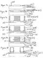
- FIGS. 1 and 2are cross-sectional views of bump formation structures according to embodiments of the present invention.
- FIGS. 3 a - fare cross-sectional views illustrating steps of forming electronic structures according to more embodiments of the present invention.
- FIGS. 4 a - fare cross-sectional views illustrating steps of forming electronic structures according to still more embodiments of the present invention.
- relative termssuch as beneath, upper, lower, top, and/or bottom may be used herein to describe one element's relationship to another element as illustrated in the figures. It will be understood that relative terms are intended to encompass different orientations of the device in addition to the orientation depicted in the figures. For example, if the device in one of the figures is turned over, elements described as below other elements would then be oriented above the other elements. The exemplary term below, can therefore, encompasses both an orientation of above and below.
- first and secondare used herein to describe various regions, layers and/or sections, these regions, layers and/or sections should not be limited by these terms. These terms are only used to distinguish one region, layer or section from another region, layer or section. Thus, a first region, layer or section discussed below could be termed a second region, layer or section, and similarly, a second region, layer or section could be termed a first region, layer or section without departing from the teachings of the present invention. Like numbers refer to like elements throughout.
- a process for forming flip chip bumps having relatively precise definitionmay be provided.
- a blanket deposition of a multilayer plating seed layercovers the wafer, and a plating template defines the bump locations.
- Selective deposition of a barrier layer and the bump metalsis performed at the template openings.
- the seed layeris removed using the barrier layer as the etch mask.
- the barrier layermay comprise a material, such as nickel, different than materials of either the seed layer or a solder layer formed on the barrier layer.
- Processes described hereinmay provide for relatively precise definition of a base of the bump by using the barrier layer rather than the solder bump as the etch mask.
- the barrier layeras the mask to remove the seed layer
- bump formation processes according to embodiments of the present inventionmay allow the formation of larger solder bumps without concern for the loss of dimensional control that may result if the bumps were used as the etch mask to define the seed layer etch.
- a bonding structure on substrate 71may include a seed layer 81 (for example, including adhesion layer 81 a and conductor layer 81 b ), a barrier metal 83 , and a bump metal 103 .
- the adhesion layer 81 amay comprise a metal such as chromium, titanium, tungsten, tantalum, aluminum, copper, iridium, platinum, titanium-tungsten, and/or alloys thereof, and/or nitrides thereof.
- the adhesion layer 81 amay include a layer of titanium and/or titanium-tungsten.
- the conductor metal 81 bmay comprise a metal such as copper, aluminum, nickel, silver, gold, and/or alloys thereof.
- the conductor layer 81 bmay include a layer of copper.
- the barrier metal 83may comprise a metal such as nickel, cobalt, platinum, gold, palladium, and/or silver.
- the barrier metal 83may include a layer of nickel-vanadium.
- the barrier metal 83may include a layer of nickel, and the layer of nickel may be doped with boron and/or phosphorous and/or the layer of nickel may be a layer of nickel-vanadium.
- an oxidation barriermay be provided between the barrier metal 83 and the bump metal 103 , and the oxidation barrier may include at least one of copper, tin, platinum, palladium, silver, and/or gold.
- the oxidation barriermay include a layer of gold. More particularly, the oxidation barrier may be provided if bump metal is not provided by plating (e.g. placement of a solid solder perform, jetting, printing, etc.) to reduce oxidation of the exposed surface before providing bump metal thereon.
- the bump metal 103may comprise a metal such as tin, silver, bismuth, antimony, lead, copper, gold, nickel, zinc, and/or alloys thereof. According to particular embodiments, the bump metal 103 may include a lead/tin solder. Other layers may also be included in structures (such as to reduce interdiffusion between the adhesion layer and the conductor metal) according to embodiments of the present invention. More particularly, a layer of a metal such as titanium, tantalum, tungsten, chromium, nickel, iridium, platinum, and/or alloys thereof may be included between the conductor metal 81 b and the adhesion layer 81 a. For example, a phased layer of chromium and copper may be included between the conductor metal 81 b and the adhesion layer 81 a.
- a sidewall of the mask 101 used to form the barrier metal 83 and the bump metal 103may be sloped at an angle, ⁇ , due to factors such as various process conditions, a Gaussian intensity profile of the light projected through the mask, and/or absorption of light by photoresist (used to form the mask) during patterning which may reduce the intensity with increasing depth. Regardless the cause, a plated bump metal 103 may have a sloped sidewall as a result. Using the bump metal 103 as an etch mask to etch the seed layer 81 may thus involve some uncertainty as to which diameter of the bump metal 103 will define the diameter of the remaining seed layer or UBM.
- the mask 101may include one or more of a photoimageable polymeric material, a metallic material including apertures therein, and/or a flexible polymeric material including apertures therein.
- the mask 101may be removed so that sidewalls of the bump metal 103 and the barrier metal 83 and portions of the seed layer 81 are exposed. Accordingly, exposed portions of the seed layer 81 may be removed using the barrier metal 83 as an etch mask. Accordingly, the barrier metal 83 may be different than the conductor metal 81 b and different than a metal of the adhesion layer 81 a.
- barrier metal 83as the etch mask may require an etchant(s) with relatively high reactivity with the conductor metal 81 b and the adhesion layer 81 a but with relatively low reactivity with the barrier metal 83 .
- the edge definitionmay be improved.
- FIGS. 3 a - fare cross-sectional views illustrating steps of forming metallurgy structures according to embodiments of the present invention.
- metal pads 303such as aluminum pads
- a passivation layer 301such as a silicon oxide layer, a silicon nitride layer, a polyimide layer, and/or other insulating layers
- substrate 305such as a semiconductor wafer including electronic devices therein.
- via holes in the passivation layer 301may expose portions of the metal pads 303 .
- a seed layer 307may be formed on the passivation layer 301 and on exposed portions of the metal pads 303 .
- the seed layer 307may include an adhesion layer 307 a and a conductivity layer 307 b.
- the adhesion layermay include a layer of a metal such as titanium, tantalum, tungsten, chromium, aluminum, copper, iridium, platinum, and/or alloys thereof and/or nitrides thereof.
- the adhesion layer 307 amay include a layer of titanium and/or titanium-tungsten.
- the conductivity layer 307 bmay include a layer of a metal such as aluminum, copper, nickel, gold, silver, and/or alloys thereof. According to particular embodiments, the conductivity layer 307 b may include a layer of copper.
- the seed layer 307may also include one or more additional layers, such as a layer to reduce interdiffusion between the adhesion layer 307 a and the conductivity layer 307 b.
- An interdiffusion layermay include a layer of a metal such as titanium, tantalum, tungsten, chromium, nickel, iridium, platinum, and/or alloys thereof and/or nitrides thereof. According to particular embodiments, an interdiffusion layer may include a phased layer of chromium and copper between the adhesion layer 307 a and the conductivity layer 307 b.
- a mask 309may be formed on the seed layer 307 thereby exposing portions of the seed layer 307 where bump metal is to be formed.
- the mask 309may be a photoimageable polymeric material, a metallic material having apertures therein, and/or a flexible polymeric material having apertures therein.
- the seed layer 307may be used as an electroplating electrode to electroplate bump metal on portions thereof exposed by the mask 309 .
- a barrier metal 311may be formed on portions of the seed layer 307 exposed by the mask 309 .
- the barrier metal 311may be a material different than a material(s) used for the seed layer 307 and different than a material(s) used for the subsequently formed bump metal.
- the barrier metalmay include a metal such as nickel, cobalt, platinum, silver, palladium, gold, and/or alloys thereof.
- the barrier metal 311may include a nickel layer, and the nickel layer may be doped with boron and/or phosphorus, and/or the nickel layer may be a nickel-vanadium layer.
- the barrier metal 311may be formed by electroplating, catalytic plating, and/or electrolytic plating.
- a bump metal 313may be formed on the barrier metal 311 .
- the bump metal 313may include a metal such as antimony, silver, bismuth, tin, lead, copper, gold, nickel, zinc, and/or alloys thereof.
- the bump metalmay include a lead/tin solder.
- the bump metalmay be formed by electroplating, electrolytic plating, and/or catalytic plating.
- the bump metal 313may be formed by filling the mask aperture(s) with a solder paste and melting (and cooling) the solder paste to fuse the paste into a solid bump.
- the bump metal 313may be formed by liquid metal jetting or screen printing. If the bump metal 313 is provided by techniques other than plating, for example, an oxidation barrier may be formed on the barrier metal 311 before providing the bump metal 313 , and the oxidation barrier may include at least one of copper, tin, platinum, palladium, silver, and/or gold. The oxidation barrier may be formed, for example, by plating through the mask 309 . Oxidation of an exposed surface can thus be reduced before providing the bump metal 313 .
- the mask 309may be removed thereby exposing portions of the seed layer 307 , and exposed portions of the seed layer 307 may be removed using the barrier layer 311 as an etching mask, as shown in FIG. 3 f.
- a wet etch chemistrymay be selected that etches the seed layer 307 selectively with respect to the barrier layer 311 . Accordingly, undercutting of the seed layer 307 may occur between the barrier layer 311 and the passivation layer 301 .
- the wet etch chemistrymay be such that the bump metal is also etched selectively with respect to the barrier layer 311 . Accordingly, surface portions of the barrier layer 311 may be exposed by the bump metal 313 adjacent edges thereof.
- the bump metal 313may be sufficiently thicker than the seed layer 307 so that exposed portions of the seed layer 307 may be removed without removing enough of the bump metal 313 to significantly effect performance thereof.
- the bump metal 313can then be reshaped by melting (i.e. reflow).
- the mask 309may be removed without forming the bump metal.
- Soldercan then be applied to one or more of the barrier layers 311 by placement of a solid solder preform(s).
- the solid solder preform(s)can be bonded to the respective barrier layer(s) 311 , for example, by pressure, heating, and/or melting.
- exposed portions of the seed layer 307may be removed using the barrier layers 311 as an etching mask before solder is provided on the barrier layers 311 . Solder can then be applied to the barrier layers 311 after removing the exposed portions of the seed layer 307 .
- an oxidation barriermay be formed on the barrier metal 311 before providing the bump metal 313 , if the bump metal 313 is provided as solid solder preforms.
- the oxidation barriermay include at least one of copper, tin, platinum, palladium, silver, and/or gold. Oxidation of an exposed surface can thus be reduced before providing the bump metal 313 .
- the oxidation barrierfor example, may be plated through the mask 309 .
- sidewalls of the mask 309 , the barrier layer 311 , and the bump metal 313may be sloped at an angle ⁇ as discussed above with respect to FIGS. 1 and 2 .
- the bump metal 313can be used to provide electrical and/or mechanical interconnection with a next level of packaging such as another substrate and/or a printed circuit board.
- the adhesion layer 307 amay include a layer of titanium and/or titanium-tungsten; the conductivity layer 307 b may include a layer of copper; the barrier metal 311 may include a layer of nickel-vanadium; an oxidation barrier on the barrier metal 311 may include a layer of gold; and the bump metal 313 may include lead-tin solder.
- the above referenced layersmay have a multi-layer structure.
- FIGS. 4 a - fare cross-sectional views illustrating steps of forming metallurgy structures according to additional embodiments of the present invention.
- metal pads 403such as aluminum pads
- a passivation layer 401such as a silicon oxide layer, a silicon nitride layer, a polyimide layer, and/or other insulating layers
- substrate 405such as a semiconductor wafer including electronic devices therein.
- via holes in the passivation layer 401may expose portions of the metal pads 403 .
- a seed layer 407may be formed on the passivation layer 401 and on exposed portions of the metal pads 403 .
- the seed layer 407may include an adhesion layer 407 a and a conductivity layer 407 b.
- the adhesion layer 407 amay include a layer of a metal such as titanium, tantalum, tungsten, chromium, aluminum, copper, iridium, platinum, and/or alloys thereof and/or nitrides thereof.
- the adhesion layer 407 amay include a layer of titanium and/or titanium-tungsten.
- the conductivity layer 407 bmay include a layer of a metal such as aluminum, copper, nickel, gold, silver, and/or alloys thereof. According to particular embodiments, the conductivity layer 407 b may include a layer of copper.
- the seed layer 407may also include one or more additional layers, such as a layer to reduce interdiffusion between the adhesion layer 407 a and the conductivity layer 407 b.
- An interdiffusion layermay include a layer of a metal such as titanium, tantalum, tungsten, chromium, nickel, iridium, platinum, and/or alloys thereof and/or nitrides thereof. According to particular embodiments, an interdiffusion layer may include a phased layer of chromium and copper between the adhesion layer 407 a and the conductivity layer 407 b.
- a mask 409may be formed on the seed layer 407 thereby exposing portions of the seed layer 407 where bump metal is to be formed.
- the mask 409may be a photoimageable polymeric material, a metallic material having apertures therein, and/or a flexible polymeric material having apertures therein.
- the seed layer 407may be used as an electroplating electrode to electroplate bump metal on portions thereof exposed by the mask 409 .
- a barrier metal 411may be formed on portions of the seed layer 407 exposed by the mask 409 .
- the barrier metal 411may be a material different than material(s) used for the seed layer 407 and different than material(s) used for the subsequently formed bump metal.
- the barrier metal 411may include a metal such as nickel, cobalt, platinum, silver, palladium, gold, and/or alloys thereof.
- the barrier metal 411may include a nickel layer, and the nickel layer may be doped with boron and/or phosphorus, and/or the nickel layer may include a layer of nickel-vanadium.
- the barrier layermay be formed by electroplating, catalytic plating, and/or electrolytic plating.
- an oxidation barriermay be provided on the barrier metal 411 before providing bump metal thereon, and the oxidation barrier may include at least one of copper, tin, platinum, palladium, silver, and/or gold.
- the oxidation barriermay be formed by plating through the mask 409 . More particularly, the oxidation barrier may include a layer of gold.
- An oxidation barriermay be provided, for example, if bump metal is provided by techniques other than plating (e.g. placement of solid solder performs, jetting, printing, etc.).
- the first mask 409may be removed, and a second mask 410 may be formed so that at least one barrier layer 411 a is exposed and so that at least one barrier layer 411 b is covered, as shown in FIG. 4 e.
- a bump metal 413may be formed on the exposed barrier metal 411 a, while the covered barrier metal 411 b is maintained free of bump metal.
- the bump metal 413may include a metal such as antimony, silver, bismuth, tin, lead, copper, gold, nickel, zinc, and/or alloys thereof According to particular embodiments of the present invention, the bump metal 413 may include a lead/tin solder.
- the bump metalmay be formed by electroplating, electrolytic plating, and/or catalytic plating.
- the bump metal 413may be formed by filling the mask aperture(s) with a solder paste and melting (and cooling) the solder paste to fuse the paste into a solid bump.
- the bump metal 413may be formed by liquid metal jetting and/or screen printing.
- the mask 410may be removed thereby exposing portions of the seed layer 407 , and exposed portions of the seed layer 407 may be removed using the barrier layers 411 a - b as etching masks, as shown in FIG. 4 f.
- a wet etch chemistrymay be selected that etches the seed layer 407 selectively with respect to the barrier layers 411 a - b. Accordingly, undercutting of the seed layer 407 may occur between the barrier layers 411 a - b and the passivation layer 401 .
- the wet etch chemistrymay be such that the bump metal is also etched selectively with respect to the barrier layer 411 a.
- the bump metal 413may be sufficiently thicker than the seed layer 407 so that exposed portions of the seed layer 407 may be removed without removing enough of the bump metal 413 to significantly effect the performance thereof.
- the bump metal 413can then be reshaped by melting (i.e. reflow).
- sidewalls of the mask 409 , the barrier layer 411 , and the bump metal 413may be sloped at an angle ⁇ as discussed above with respect to FIGS. 1 and 2 .
- the bump metal 413can be used to provide electrical and/or mechanical interconnection with a next level of packaging such as another substrate and/or a printed circuit board.
- the adhesion layer 407 amay include a layer of titanium and/or titanium-tungsten; the conductivity layer 407 b may include a layer of copper; the barrier metal 411 a - b may include layers of nickel-vanadium; oxidation barriers on the barrier metal 411 a - b may include a layer of gold; and the bump metal 413 may include lead-tin solder.
- the above referenced layersmay have a multi-layer structure.
- a bump metal 413may be selectively plated on a first barrier metal 411 a, while a second barrier metal 411 b is maintained free of bump metal. Accordingly, bump metal 413 may be used to provide a solder connection to another substrate (such as a printed circuit board or another semiconductor substrate), while the barrier layer 411 b (which is maintained free of bump metal) may be used to provide different interconnects such as wire bond interconnects.
- all of barrier layers 411may be maintained free of bump metal until after removing exposed portions of the seed layer 407 using the barrier layers 411 as etch masks.
- solid solder preformssuch as preformed solder balls
- the solid solder preform(s)can be bonded to the respective barrier layer (s) 411 , for example, by pressure, heating, and/or melting.
- bump metalmay be provided on another substrate to which the substrate 405 is to be bonded, and the barrier layers 411 may be bonded to the bump metal provided on the other substrate.
- bump metal 413may be selectively formed on barrier layer 411 a without providing a second mask 410 . More particularly, the mask 409 exposing both barrier layers 411 a - b may be maintained, and bump metal 413 may be selectively formed on barrier layer 411 a, for example, using selective metal jetting and/or selective screen printing into the hole exposing the barrier layer 411 a without jetting or screen printing into the hole exposing the barrier layer 411 b. Accordingly, the structure of FIG. 4 f may be provided without requiring the second mask 410 .
- oxidation barriersmay be provided on the barrier layers 411 a - b as discussed above.
- the oxidation barriersmay include layers of at least one of copper, tin, platinum, palladium, silver, and/or gold, and the oxidation barriers can be plated through the mask 409 after plating the barrier layers 411 a - b.
- the oxidation barriersmay include layers of gold. Separate oxidation layers, however, may not be required in the barrier layers 411 a - b include a metal such as gold, silver, platinum, and/or palladium that is resistant to oxidation.
- FIGS. 5 a - hare cross-sectional views illustrating steps of forming metallurgy structures according to additional embodiments of the present invention.
- metal pads 503such as aluminum pads
- a passivation layer 501such as a silicon oxide layer, a silicon nitride layer, a polyimide layer, and/or other insulating layers
- substrate 505such as a semiconductor wafer including electronic devices therein.
- via holes in the passivation layer 501may expose portions of the metal pads 503 .
- a seed layer 507may be formed on the passivation layer 501 and on exposed portions of the metal pads 503 .
- the seed layer 507may include an adhesion layer 507 a and a conductivity layer 507 b.
- the adhesion layer 507 amay include a layer of a metal such as titanium, tantalum, tungsten, chromium, aluminum, copper, iridium, and/or platinum, and/or alloys thereof and/or nitrides thereof.
- the adhesion layer 507 amay include a layer of titanium and/or titanium-tungsten.
- the conductivity layer 507 bmay include a layer of a metal such as aluminum, copper, nickel, gold, silver, and/or alloys thereof. According to particular embodiments, the conductivity layer 507 b may include a layer of copper.
- the seed layer 507may also include one or more additional layers, such as a layer to reduce interdiffusion between the adhesion layer 507 a and the conductivity layer 507 b.
- An interdiffusion layermay include a layer of a metal such as titanium, tantalum, tungsten, chromium, nickel, iridium, platinum, and/or alloys thereof and/or nitrides thereof. According to particular embodiments, an interdiffusion layer may include a phased layer of chromium and copper between the adhesion layer 507 a and the conductivity layer 507 b.
- a mask 509may be formed on the seed layer 507 thereby exposing portions of the seed layer 507 where bump metal is to be formed.
- the mask 509may be a photoimageable polymeric material, a metallic material having apertures therein, and/or a flexible polymeric material having apertures therein.
- the seed layer 507may be used as an electroplating electrode to electroplate a barrier metal on portions thereof exposed by the mask 509 .
- a barrier metal 511may be formed on portions of the seed layer 507 exposed by the mask 509 .
- the barrier metal 511may include a layer of a material different than material(s) used for the seed layer 507 and different than material(s) used for a subsequently provided bump metal.
- the barrier metal 511may include a metal such as nickel, cobalt, platinum, silver, palladium, gold, and/or alloys thereof
- the barrier metal 511may include a nickel layer, and the nickel layer may be doped with boron and/or phosphorus.
- the nickel layermay include a layer of nickel-vanadium.
- the barrier layermay be formed by electroplating, catalytic plating, and/or electrolytic plating.
- an oxidation barriermay be plated through the mask 509 on the barrier metal 511 , and the oxidation barrier may include at least one of copper, tin, platinum, palladium, silver, and/or gold. More particularly, the oxidation barrier may include a layer of gold.
- the barrier metal 511may include a layer of nickel-vanadium, and the oxidation layer may include a layer of gold. Accordingly, oxidation of an exposed surface can be reduced prior to provide bump metal thereon.
- an oxidation barriermay be considered a part of the barrier metal. A separate oxidation barrier may not be required if the barrier metal 511 includes a metal such as platinum, palladium, silver, and/or gold that is resistant to oxidation.
- the mask 509may then be removed as shown in FIG. 5 e thereby exposing portions of the seed layer 507 , and exposed portions of the seed layer 507 may be removed using the barrier layers 511 as etching masks, as shown in FIG. 5 f.
- a wet etch chemistrymay be selected that etches the seed layer 507 selectively with respect to the barrier layers 511 . Accordingly, undercutting of the seed layer 507 may occur between the barrier layers 511 and the passivation layer 501 .
- Bump metalmay be provided on the barrier layers 511 (and/or oxidation barriers) before or after removing exposed portions of the seed layer.
- the adhesion layer 507 amay include a layer of titanium and/or titanium-tungsten; the conductivity layer 507 b may include a layer of copper; the barrier metal 511 may include a layer of nickel-vanadium; an oxidation barrier on the barrier metal 511 may include a layer of gold; and bump metal 513 , 513 ′ may include lead-tin solder.
- the above referenced layersmay have a multi-layer structure.
- all of the barrier layers 511 (and/or oxidation barriers)may thus be maintained free of bump metal until after removing exposed portions of the seed layer 507 using the barrier layers 511 (and/or oxidation barriers) as etch masks.
- solid solder preforms 513such as preformed solder balls
- the solid solder preforms 513can be bonded to the respective barrier layers 511 (and/or oxidation barriers), for example, by pressure, heating, and/or melting.
- bump metalmay be selectively provided on barrier layers 511 (and/or oxidation barriers), for example, using selective metal jetting and/or selective screen printing.
- the bump metal 513may include a metal such as antimony, silver, bismuth, tin, lead, copper, gold, nickel, zinc, and/or alloys thereof.
- the bump metal 513may include a lead/tin solder.
- the solid solder performs 513 or other bump metalcan be used to provide electrical and/or mechanical interconnection with a next level of packaging such as another substrate and/or a printed circuit board.
- the barrier layers 511may be defined to include oxidation barrier layers if separate oxidation barrier layers are provided thereon.
- all of the barrier layers 511 (and/or oxidation barriers)may thus be maintained free of bump metal until after removing exposed portions of the seed layer 507 using the barrier layers 511 (and/or oxidation barriers) as etch masks.
- bump metal 513 ′may be provided on another substrate 521 to which the substrate 505 is to be bonded, and the barrier layers 511 (and/or oxidation barriers) may be bonded to the bump metal 513 ′ provided on the other substrate.
- the bump metal 513 ′ on the other substrate 521can be bonded to respective barrier layers 511 (and/or oxidation barriers), for example, by pressure, heating, and/or melting.
- the bump metal 513 ′may include a metal such as antimony, silver, bismuth, tin, lead, copper, gold, nickel, zinc, and/or alloys thereof.
- the bump metal 513 ′may include a lead/tin solder.
- the bump metal 513 ′may be provided on respective pads 517 of the substrate 521 by plating, jetting, screen printing, and/or placement of preformed solder balls prior to mating with barrier layers 511 (and/or oxidation barriers) of substrate 505 .
- the pads 517 of the substrate 521may include adhesion layers, conduction layers, and/or barrier layers as discussed above with respect to layers 507 a, 507 b, and/or 511 of the substrate 505 .
Landscapes
- Engineering & Computer Science (AREA)
- Microelectronics & Electronic Packaging (AREA)
- Manufacturing & Machinery (AREA)
- Computer Hardware Design (AREA)
- Power Engineering (AREA)
- Internal Circuitry In Semiconductor Integrated Circuit Devices (AREA)
Abstract
Description
- This application claims the benefit of priority from U.S. Provisional Patent Application No. 60/552,051 filed on Mar. 10, 2004, the disclosure of which is hereby incorporated herein by reference in its entirety.
- The present application relates to the field of electronics, and more particularly, to methods of forming interconnection bumps and related structures.
- C4 (Controlled-Collapse Chip Connection) is a means of connecting IC (integrated circuit) chips to substrates in electronic packages. Moreover, C4 is a flip-chip technology in which the interconnections are small solder balls on the chip surface. Because it is an area array, C4 technology may provide relatively high densities for chip interconnections.
- C4 technology has used since the 1960s and has proven highly reliable in the semiconductor field. Historically, PbSn (lead-tin) solder has been evaporated through a metal mask. In the 1990s, electrochemical fabrication of C4 interconnections was introduced (See, for example, M. Datta, et al., “Electrochemical Fabrication of Mechanically Robust PbSn Interconnections”, J. Electrochem. Soc., 142, 3779 (1995); U.S. Pat. No. 5,162,257 to Yung; and WO 96/30933). Electroplating may be more extendible than evaporation to small C4-pad dimensions, and may provide closer pad spacing, larger wafers, and/or lower-melting solders (having a higher content of Sn).
- U.S. Pat. No. 5,937,320 discusses barrier layers for electroplated PbSn eutectic solder joints. An electrochemically fabricated C4 interconnection may have a barrier layer between the electroplated tin-rich solder bump and the ball-limiting metallurgy that protects the terminal metal in the ball-limiting metallurgy from attack by the Sn in the solder. The barrier layer may be electroplated through the same photoresist mask as the solder and thus may not require a separate patterning step. A thin layer of electroplated nickel may serve as a reliable barrier layer between a copper-based ball-limiting metallurgy and a tin-lead (PbSn) eutectic C4 ball. U.S. Pat. No. 6,622,907 discusses a sacrificial seed layer process for forming C4 solder balls. The disclosures of U.S. Pat. No. 5,937,320 and U.S. Pat. No. 6,622,907 are hereby incorporated herein in their entirety by reference.
- According to embodiments of the present invention, forming an electronic structure may include forming a seed layer on a substrate, and forming a mask on the seed layer wherein the mask includes an aperture therein exposing a portion of the seed layer. A barrier layer may be formed on the exposed portion of the seed layer, a bump metal may be formed on the barrier layer, and the mask may be removed. In addition, portions of the seed layer may be selectively removed using the barrier layer as an etch mask.
- The bump metal may be formed subsequent to selectively removing portions of the seed layer using the barrier layer as an etch mask. More particularly, forming the bump metal may include placing a solid solder preform on the barrier layer. In addition, selectively removing portions of the seed layer may include etching portions of the seed layer exposed by the barrier layer using an etch chemistry that etches the seed layer selectively with respect to the barrier layer.
- Forming the bump metal may precede removing the mask and selectively removing portions of the seed layer. More particularly, selectively removing portions of the seed layer may include etching portions of the seed layer exposed by the barrier layer using an etch chemistry that etches the seed layer selectively with respect to the barrier layer and that etches the bump metal selectively with respect to the barrier layer. After selectively removing portions of the seed layer, a surface portion of the barrier layer may be exposed adjacent the bump metal adjacent an edge of the barrier layer. Moreover, forming the bump metal may include plating the bump metal on the barrier layer.
- The barrier layer may include a material different than the seed layer and different than the bump material. In addition, the seed layer may include an adhesion layer on the substrate and a conductivity layer on the adhesion layer so that the adhesion layer is between the conductivity layer and the substrate. The adhesion layer may include at least one of titanium, tantalum, tungsten, chromium, aluminum, copper, iridium, platinum, and/or alloys thereof, and/or nitrides thereof. The conductivity layer may include at least one of aluminum, copper, nickel, gold, silver, and/or alloys thereof. The barrier layer may include at least one of nickel, cobalt, platinum, silver, palladium, gold, and/or alloys thereof. For example, the barrier layer may include a layer of nickel-vanadium (Ni:Va). The bump metal may include at least one of antimony, silver, bismuth, tin, lead, copper, silver, gold, nickel, zinc, and/or alloys thereof. In addition, an oxidation barrier may be formed on the barrier layer before forming the bump metal, and the oxidation barrier may include a material different than the barrier layer and different than the bump metal. More particularly, the oxidation barrier may be provided if bump metal is not provided by plating (e.g. placement of a solid solder perform, jetting, printing, etc.). For example, the oxidation barrier may include at least one of copper, tin, platinum, palladium, silver, and/or gold. Moreover, each of the seed layer, the adhesion layer, the conductivity layer, the barrier layer, the oxidation barrier, and/or the bump metal may include a multi-layer structure. According to particular embodiments, the adhesion layer may include a layer of titanium and/or titanium-tungsten; the conductivity layer may include a layer of copper; the barrier layer may include a layer of nickel-vanadium; the oxidation barrier may include a layer of gold; and the bump metal may include solder.
- According to additional embodiments of the present invention, an electronic structure may include a substrate, a seed layer on the substrate, and a barrier layer on the seed layer so that the seed layer is between the substrate and the barrier layer. A bump metal may be provided on the barrier layer so that the barrier layer is between the bump metal and the seed layer. In addition, the barrier layer may define a lip extending beyond the bump metal so that surface portions of the barrier layer are exposed adjacent the bump metal along an edge of the barrier layer.
- The lip of the barrier layer may extend beyond the seed layer so that the seed layer is set back from the lip of the barrier layer between the barrier layer and the substrate. In addition, the barrier layer may include a material different than the seed layer and different than the bump material. The seed layer may include an adhesion layer on the substrate and a conductivity layer on the adhesion layer so that the adhesion layer is between the conductivity layer and the substrate.
- The adhesion layer may include at least one of titanium, tantalum, tungsten, chromium, aluminum, copper, iridium, platinum, and/or alloys thereof, and/or nitrides thereof. The conductivity layer may include at least one of aluminum, copper, nickel, gold, silver, and/or alloys thereof. The barrier layer may include at least one of nickel, cobalt, platinum, silver, palladium, gold, and/or alloys thereof. For example, the barrier layer may include a layer of nickel-vanadium (Ni:Va). The bump metal may include at least one of antimony, silver, bismuth, tin, lead, copper, silver, gold, nickel, zinc, and/or alloys thereof. In addition, an oxidation barrier may be formed on the barrier layer before providing the bump metal, and the oxidation barrier may include a material different than the barrier layer and different than the bump metal. More particularly, the oxidation barrier may be provided if bump metal is not provided by plating (e.g. placement of a solid solder perform, jetting, printing, etc.). For example, the oxidation barrier may include at least one of copper, tin, platinum, palladium, silver, and/or gold. Moreover, each of the seed layer, the adhesion layer, the conductivity layer, the barrier layer, the oxidation barrier, and/or the bump metal may include a multi-layer structure. According to particular embodiments, the adhesion layer may include a layer of titanium and/or titanium-tungsten; the conductivity layer may include a layer of copper; the barrier layer may include a layer of nickel-vanadium; and the bump metal may include solder.
- According to still additional embodiments of the present invention, forming an electronic structure may include forming a seed layer on a substrate, and selectively forming a barrier layer on a portion of the seed layer. More particularly, the barrier layer and the seed layer may include different materials, and the barrier layer may include at least one of nickel, cobalt, platinum, silver, palladium, gold, and/or alloys thereof. For example, the barrier layer may include a layer of nickel-vanadium (Ni:Va). Portions of the seed layer may be selectively removed using the barrier layer as an etching mask, and a bump metal may be provided on the barrier layer opposite the seed layer, and the bump metal and the barrier layer may include different materials.
- Providing the bump metal, for example, may include placing a solid solder preform on the barrier layer after selectively removing portions of the seed layer. In an alternative, the bump metal may include a bump metal on a second substrate, and providing the bump metal on the barrier layer may include bonding the barrier layer with the bump metal on the second substrate after selectively removing portions of the seed layer. In still another alternative, providing the bump metal may include providing the bump metal on the barrier layer before selectively removing portions of the seed layer. Moreover, selectively removing portions of the seed layer may include etching portions of the seed layer exposed by the barrier layer using an etch chemistry that etches the seed layer selectively with respect to the barrier layer. In addition, the seed layer may include adhesion and conductivity layers.
- In addition, an oxidation barrier may be formed on the barrier layer before providing the bump metal, and the oxidation barrier may include a material different than a material of the barrier layer and different that a material of the bump metal. More particularly, the oxidation barrier may be provided if bump metal is not provided by plating (e.g. placement of a solid solder perform, jetting, printing, etc.). For example, the oxidation barrier may include at least one of copper, tin, platinum, palladium, silver, and/or gold. Moreover, each of the seed layer, the adhesion layer, the conductivity layer, the barrier layer, the oxidation layer, and/or the bump metal may include a multi-layer structure. According to particular embodiments, the adhesion layer may include a layer of titanium and/or titanium-tungsten; the conductivity layer may include a layer of copper; the barrier layer may include a layer of nickel-vanadium; the oxidation barrier may include a layer of gold; and the bump metal may include solder.
FIGS. 1 and 2 are cross-sectional views of bump formation structures according to embodiments of the present invention.FIGS. 3 a-fare cross-sectional views illustrating steps of forming electronic structures according to more embodiments of the present invention.FIGS. 4 a-fare cross-sectional views illustrating steps of forming electronic structures according to still more embodiments of the present invention.- The present invention now will be described more fully hereinafter with reference to the accompanying drawings, in which embodiments of the invention are shown. This invention may, however, be embodied in many different forms and should not be construed as limited to the embodiments set forth herein. Rather, these embodiments are provided so that this disclosure will be thorough and complete, and will fully convey the scope of the invention to those skilled in the art.
- In the drawings, the thickness of layers and regions are exaggerated for clarity. It will also be understood that when an element such as a layer, region or substrate is referred to as being on another element, it can be directly on the other element or intervening elements may also be present. In contrast, if an element such as a layer, region or substrate is referred to as being directly on another element, then no other intervening elements are present. Similarly, when an element such as a layer, region or substrate is referred to as being coupled or connected to/with another element, it can be directly coupled or connected to/with the other element or intervening elements may also be present. In contrast, if an element such as a layer, region or substrate is referred to as being directly coupled or connected to/with another element, then no other intervening elements are present. As used herein, the term “and/or” includes any and all combinations of one or more of the associated listed items. The symbol “/” is also used as a shorthand notation for “and/or”.
- Furthermore, relative terms, such as beneath, upper, lower, top, and/or bottom may be used herein to describe one element's relationship to another element as illustrated in the figures. It will be understood that relative terms are intended to encompass different orientations of the device in addition to the orientation depicted in the figures. For example, if the device in one of the figures is turned over, elements described as below other elements would then be oriented above the other elements. The exemplary term below, can therefore, encompasses both an orientation of above and below.
- It will be understood that although the terms first and second are used herein to describe various regions, layers and/or sections, these regions, layers and/or sections should not be limited by these terms. These terms are only used to distinguish one region, layer or section from another region, layer or section. Thus, a first region, layer or section discussed below could be termed a second region, layer or section, and similarly, a second region, layer or section could be termed a first region, layer or section without departing from the teachings of the present invention. Like numbers refer to like elements throughout.
- The terminology used herein is for the purpose of describing particular embodiments only and is not intended to be limiting of the invention. As used herein, the singular forms “a”, “an” and “the” are intended to include the plural forms as well, unless the context clearly indicates otherwise. It will be further understood that the terms “comprises” and/or “comprising,” when used in this specification, specify the presence of stated features, integers, steps, operations, elements, and/or components, but do not preclude the presence or addition of one or more other features, integers, steps, operations, elements, components, and/or groups thereof.
- Unless otherwise defined, all terms (including technical and scientific terms) used herein have the same meaning as commonly understood by one of ordinary skill in the art to which this invention belongs. It will be further understood that terms, such as those defined in commonly used dictionaries, should be interpreted as having a meaning that is consistent with their meaning in the context of the relevant art and will not be interpreted in an idealized or overly formal sense unless expressly so defined herein.
- According to embodiments of the present invention, a process for forming flip chip bumps having relatively precise definition may be provided. According to particular embodiments, a blanket deposition of a multilayer plating seed layer covers the wafer, and a plating template defines the bump locations. Selective deposition of a barrier layer and the bump metals is performed at the template openings. After removal of the template, the seed layer is removed using the barrier layer as the etch mask. The barrier layer may comprise a material, such as nickel, different than materials of either the seed layer or a solder layer formed on the barrier layer.
- Processes described herein may provide for relatively precise definition of a base of the bump by using the barrier layer rather than the solder bump as the etch mask. By using the barrier layer as the mask to remove the seed layer, bump formation processes according to embodiments of the present invention may allow the formation of larger solder bumps without concern for the loss of dimensional control that may result if the bumps were used as the etch mask to define the seed layer etch.
- As shown in
FIG. 1 , a bonding structure onsubstrate 71 may include a seed layer81 (for example, including adhesion layer81aand conductor layer81b), abarrier metal 83, and abump metal 103. By way of example, the adhesion layer81amay comprise a metal such as chromium, titanium, tungsten, tantalum, aluminum, copper, iridium, platinum, titanium-tungsten, and/or alloys thereof, and/or nitrides thereof. For example, the adhesion layer81amay include a layer of titanium and/or titanium-tungsten. The conductor metal81bmay comprise a metal such as copper, aluminum, nickel, silver, gold, and/or alloys thereof. For example, the conductor layer81bmay include a layer of copper. Thebarrier metal 83 may comprise a metal such as nickel, cobalt, platinum, gold, palladium, and/or silver. For example, thebarrier metal 83 may include a layer of nickel-vanadium. According to other embodiments, thebarrier metal 83 may include a layer of nickel, and the layer of nickel may be doped with boron and/or phosphorous and/or the layer of nickel may be a layer of nickel-vanadium. In addition, an oxidation barrier may be provided between thebarrier metal 83 and thebump metal 103, and the oxidation barrier may include at least one of copper, tin, platinum, palladium, silver, and/or gold. For example, the oxidation barrier may include a layer of gold. More particularly, the oxidation barrier may be provided if bump metal is not provided by plating (e.g. placement of a solid solder perform, jetting, printing, etc.) to reduce oxidation of the exposed surface before providing bump metal thereon. - The
bump metal 103 may comprise a metal such as tin, silver, bismuth, antimony, lead, copper, gold, nickel, zinc, and/or alloys thereof. According to particular embodiments, thebump metal 103 may include a lead/tin solder. Other layers may also be included in structures (such as to reduce interdiffusion between the adhesion layer and the conductor metal) according to embodiments of the present invention. More particularly, a layer of a metal such as titanium, tantalum, tungsten, chromium, nickel, iridium, platinum, and/or alloys thereof may be included between the conductor metal81band the adhesion layer81a.For example, a phased layer of chromium and copper may be included between the conductor metal81band the adhesion layer81a. - As further shown in
FIG. 1 , a sidewall of themask 101 used to form thebarrier metal 83 and the bump metal103 (such as by electroplating) may be sloped at an angle, θ, due to factors such as various process conditions, a Gaussian intensity profile of the light projected through the mask, and/or absorption of light by photoresist (used to form the mask) during patterning which may reduce the intensity with increasing depth. Regardless the cause, a platedbump metal 103 may have a sloped sidewall as a result. Using thebump metal 103 as an etch mask to etch theseed layer 81 may thus involve some uncertainty as to which diameter of thebump metal 103 will define the diameter of the remaining seed layer or UBM. Themask 101, for example, may include one or more of a photoimageable polymeric material, a metallic material including apertures therein, and/or a flexible polymeric material including apertures therein. - As shown in
FIG. 2 , themask 101 may be removed so that sidewalls of thebump metal 103 and thebarrier metal 83 and portions of theseed layer 81 are exposed. Accordingly, exposed portions of theseed layer 81 may be removed using thebarrier metal 83 as an etch mask. Accordingly, thebarrier metal 83 may be different than the conductor metal81band different than a metal of the adhesion layer81a. - Using the
barrier metal 83 as the etch mask may require an etchant(s) with relatively high reactivity with the conductor metal81band the adhesion layer81abut with relatively low reactivity with thebarrier metal 83. With this approach, the edge definition may be improved. FIGS. 3 a-fare cross-sectional views illustrating steps of forming metallurgy structures according to embodiments of the present invention. As shown inFIG. 3 a,metal pads303 (such as aluminum pads) and a passivation layer301 (such as a silicon oxide layer, a silicon nitride layer, a polyimide layer, and/or other insulating layers) may be provided on a substrate305 (such as a semiconductor wafer including electronic devices therein). As shown, via holes in thepassivation layer 301 may expose portions of themetal pads 303.- As shown in
FIG. 3 b,aseed layer 307 may be formed on thepassivation layer 301 and on exposed portions of themetal pads 303. By way of example, theseed layer 307 may include an adhesion layer307aand a conductivity layer307b.The adhesion layer may include a layer of a metal such as titanium, tantalum, tungsten, chromium, aluminum, copper, iridium, platinum, and/or alloys thereof and/or nitrides thereof. According to particular embodiments, the adhesion layer307amay include a layer of titanium and/or titanium-tungsten. The conductivity layer307bmay include a layer of a metal such as aluminum, copper, nickel, gold, silver, and/or alloys thereof. According to particular embodiments, the conductivity layer307bmay include a layer of copper. Theseed layer 307 may also include one or more additional layers, such as a layer to reduce interdiffusion between the adhesion layer307aand the conductivity layer307b.An interdiffusion layer, for example, may include a layer of a metal such as titanium, tantalum, tungsten, chromium, nickel, iridium, platinum, and/or alloys thereof and/or nitrides thereof. According to particular embodiments, an interdiffusion layer may include a phased layer of chromium and copper between the adhesion layer307aand the conductivity layer307b. - As shown in
FIG. 3 c,amask 309 may be formed on theseed layer 307 thereby exposing portions of theseed layer 307 where bump metal is to be formed. Themask 309, for example, may be a photoimageable polymeric material, a metallic material having apertures therein, and/or a flexible polymeric material having apertures therein. According to particular embodiments, theseed layer 307 may be used as an electroplating electrode to electroplate bump metal on portions thereof exposed by themask 309. - As shown in
FIG. 3 d,abarrier metal 311 may be formed on portions of theseed layer 307 exposed by themask 309. Moreover, thebarrier metal 311 may be a material different than a material(s) used for theseed layer 307 and different than a material(s) used for the subsequently formed bump metal. The barrier metal, for example, may include a metal such as nickel, cobalt, platinum, silver, palladium, gold, and/or alloys thereof. According to particular embodiments of the present invention, thebarrier metal 311 may include a nickel layer, and the nickel layer may be doped with boron and/or phosphorus, and/or the nickel layer may be a nickel-vanadium layer. Moreover, thebarrier metal 311 may be formed by electroplating, catalytic plating, and/or electrolytic plating. - As shown in
FIG. 3 e,abump metal 313 may be formed on thebarrier metal 311. Thebump metal 313, for example, may include a metal such as antimony, silver, bismuth, tin, lead, copper, gold, nickel, zinc, and/or alloys thereof. According to particular embodiments of the present invention, the bump metal may include a lead/tin solder. Moreover, the bump metal may be formed by electroplating, electrolytic plating, and/or catalytic plating. In another alternative, thebump metal 313 may be formed by filling the mask aperture(s) with a solder paste and melting (and cooling) the solder paste to fuse the paste into a solid bump. According to other alternatives, thebump metal 313 may be formed by liquid metal jetting or screen printing. If thebump metal 313 is provided by techniques other than plating, for example, an oxidation barrier may be formed on thebarrier metal 311 before providing thebump metal 313, and the oxidation barrier may include at least one of copper, tin, platinum, palladium, silver, and/or gold. The oxidation barrier may be formed, for example, by plating through themask 309. Oxidation of an exposed surface can thus be reduced before providing thebump metal 313. - The
mask 309 may be removed thereby exposing portions of theseed layer 307, and exposed portions of theseed layer 307 may be removed using thebarrier layer 311 as an etching mask, as shown inFIG. 3 f.In particular, a wet etch chemistry may be selected that etches theseed layer 307 selectively with respect to thebarrier layer 311. Accordingly, undercutting of theseed layer 307 may occur between thebarrier layer 311 and thepassivation layer 301. Moreover, the wet etch chemistry may be such that the bump metal is also etched selectively with respect to thebarrier layer 311. Accordingly, surface portions of thebarrier layer 311 may be exposed by thebump metal 313 adjacent edges thereof. More particularly, thebump metal 313 may be sufficiently thicker than theseed layer 307 so that exposed portions of theseed layer 307 may be removed without removing enough of thebump metal 313 to significantly effect performance thereof. Thebump metal 313 can then be reshaped by melting (i.e. reflow). - In an alternative, the
mask 309 may be removed without forming the bump metal. Solder can then be applied to one or more of the barrier layers311 by placement of a solid solder preform(s). The solid solder preform(s) can be bonded to the respective barrier layer(s)311, for example, by pressure, heating, and/or melting. Moreover, exposed portions of theseed layer 307 may be removed using the barrier layers311 as an etching mask before solder is provided on the barrier layers311. Solder can then be applied to the barrier layers311 after removing the exposed portions of theseed layer 307. As discussed above, an oxidation barrier may be formed on thebarrier metal 311 before providing thebump metal 313, if thebump metal 313 is provided as solid solder preforms. The oxidation barrier, for example, may include at least one of copper, tin, platinum, palladium, silver, and/or gold. Oxidation of an exposed surface can thus be reduced before providing thebump metal 313. The oxidation barrier, for example, may be plated through themask 309. - While not shown in
FIGS. 3 a-ffor the sake of clarity, sidewalls of themask 309, thebarrier layer 311, and thebump metal 313 may be sloped at an angle θ as discussed above with respect toFIGS. 1 and 2 . Moreover, thebump metal 313 can be used to provide electrical and/or mechanical interconnection with a next level of packaging such as another substrate and/or a printed circuit board. According to particular embodiments of the present invention, the adhesion layer307amay include a layer of titanium and/or titanium-tungsten; the conductivity layer307bmay include a layer of copper; thebarrier metal 311 may include a layer of nickel-vanadium; an oxidation barrier on thebarrier metal 311 may include a layer of gold; and thebump metal 313 may include lead-tin solder. Moreover, one or more of the above referenced layers may have a multi-layer structure. FIGS. 4 a-fare cross-sectional views illustrating steps of forming metallurgy structures according to additional embodiments of the present invention. As shown inFIG. 4 a,metal pads403 (such as aluminum pads) and a passivation layer401 (such as a silicon oxide layer, a silicon nitride layer, a polyimide layer, and/or other insulating layers) may be provided on a substrate405 (such as a semiconductor wafer including electronic devices therein). As shown, via holes in thepassivation layer 401 may expose portions of themetal pads 403.- As shown in
FIG. 4 b,aseed layer 407 may be formed on thepassivation layer 401 and on exposed portions of themetal pads 403. By way of example, theseed layer 407 may include anadhesion layer 407aand a conductivity layer407b.Theadhesion layer 407amay include a layer of a metal such as titanium, tantalum, tungsten, chromium, aluminum, copper, iridium, platinum, and/or alloys thereof and/or nitrides thereof. According to particular embodiments, theadhesion layer 407amay include a layer of titanium and/or titanium-tungsten. The conductivity layer407bmay include a layer of a metal such as aluminum, copper, nickel, gold, silver, and/or alloys thereof. According to particular embodiments, the conductivity layer407bmay include a layer of copper. Theseed layer 407 may also include one or more additional layers, such as a layer to reduce interdiffusion between theadhesion layer 407aand the conductivity layer407b.An interdiffusion layer, for example, may include a layer of a metal such as titanium, tantalum, tungsten, chromium, nickel, iridium, platinum, and/or alloys thereof and/or nitrides thereof. According to particular embodiments, an interdiffusion layer may include a phased layer of chromium and copper between theadhesion layer 407aand the conductivity layer407b. - As shown in
FIG. 4 c,amask 409 may be formed on theseed layer 407 thereby exposing portions of theseed layer 407 where bump metal is to be formed. Themask 409, for example, may be a photoimageable polymeric material, a metallic material having apertures therein, and/or a flexible polymeric material having apertures therein. According to particular embodiments, theseed layer 407 may be used as an electroplating electrode to electroplate bump metal on portions thereof exposed by themask 409. - As shown in
FIG. 4 d,a barrier metal411 may be formed on portions of theseed layer 407 exposed by themask 409. Moreover, the barrier metal411 may be a material different than material(s) used for theseed layer 407 and different than material(s) used for the subsequently formed bump metal. The barrier metal411, for example, may include a metal such as nickel, cobalt, platinum, silver, palladium, gold, and/or alloys thereof. According to particular embodiments of the present invention, the barrier metal411 may include a nickel layer, and the nickel layer may be doped with boron and/or phosphorus, and/or the nickel layer may include a layer of nickel-vanadium. Moreover, the barrier layer may be formed by electroplating, catalytic plating, and/or electrolytic plating. In addition, an oxidation barrier may be provided on the barrier metal411 before providing bump metal thereon, and the oxidation barrier may include at least one of copper, tin, platinum, palladium, silver, and/or gold. The oxidation barrier may be formed by plating through themask 409. More particularly, the oxidation barrier may include a layer of gold. An oxidation barrier may be provided, for example, if bump metal is provided by techniques other than plating (e.g. placement of solid solder performs, jetting, printing, etc.). - The
first mask 409 may be removed, and a second mask410 may be formed so that at least onebarrier layer 411ais exposed and so that at least one barrier layer411bis covered, as shown inFIG. 4 e.A bump metal413 may be formed on the exposedbarrier metal 411a,while the covered barrier metal411bis maintained free of bump metal. The bump metal413, for example, may include a metal such as antimony, silver, bismuth, tin, lead, copper, gold, nickel, zinc, and/or alloys thereof According to particular embodiments of the present invention, the bump metal413 may include a lead/tin solder. Moreover, the bump metal may be formed by electroplating, electrolytic plating, and/or catalytic plating. In another alternative, the bump metal413 may be formed by filling the mask aperture(s) with a solder paste and melting (and cooling) the solder paste to fuse the paste into a solid bump. In still other embodiments, the bump metal413 may be formed by liquid metal jetting and/or screen printing. - The mask410 may be removed thereby exposing portions of the
seed layer 407, and exposed portions of theseed layer 407 may be removed using the barrier layers411a-bas etching masks, as shown inFIG. 4 f.In particular, a wet etch chemistry may be selected that etches theseed layer 407 selectively with respect to the barrier layers411a-b.Accordingly, undercutting of theseed layer 407 may occur between the barrier layers411a-band thepassivation layer 401. Moreover, the wet etch chemistry may be such that the bump metal is also etched selectively with respect to thebarrier layer 411a.Accordingly, surface portions of thebarrier layer 411amay be exposed by the bump metal413 adjacent edges thereof. More particularly, the bump metal413 may be sufficiently thicker than theseed layer 407 so that exposed portions of theseed layer 407 may be removed without removing enough of the bump metal413 to significantly effect the performance thereof. The bump metal413 can then be reshaped by melting (i.e. reflow). - While not shown in
FIGS. 4 a-ffor the sake of clarity, sidewalls of themask 409, the barrier layer411, and the bump metal413 may be sloped at an angle θ as discussed above with respect toFIGS. 1 and 2 . Moreover, the bump metal413 can be used to provide electrical and/or mechanical interconnection with a next level of packaging such as another substrate and/or a printed circuit board. According to particular embodiments of the present invention, theadhesion layer 407amay include a layer of titanium and/or titanium-tungsten; the conductivity layer407bmay include a layer of copper; the barrier metal411a-bmay include layers of nickel-vanadium; oxidation barriers on the barrier metal411a-bmay include a layer of gold; and the bump metal413 may include lead-tin solder. Moreover, one or more of the above referenced layers may have a multi-layer structure. - As discussed above with respect to
FIGS. 4 a-f,a bump metal413 may be selectively plated on afirst barrier metal 411a,while a second barrier metal411bis maintained free of bump metal. Accordingly, bump metal413 may be used to provide a solder connection to another substrate (such as a printed circuit board or another semiconductor substrate), while the barrier layer411b(which is maintained free of bump metal) may be used to provide different interconnects such as wire bond interconnects. - According to additional embodiments of the present invention, all of barrier layers411 may be maintained free of bump metal until after removing exposed portions of the
seed layer 407 using the barrier layers411 as etch masks. By way of example, solid solder preforms (such as preformed solder balls) may be placed on some or all of the barrier layers411 after removing exposed portions of theseed layer 407 using the barrier layers411 as etch masks. The solid solder preform(s) can be bonded to the respective barrier layer (s)411, for example, by pressure, heating, and/or melting. In an alternative, bump metal may be provided on another substrate to which thesubstrate 405 is to be bonded, and the barrier layers411 may be bonded to the bump metal provided on the other substrate. - According to still additional embodiments of the present invention, bump metal413 may be selectively formed on
barrier layer 411awithout providing a second mask410. More particularly, themask 409 exposing both barrier layers411a-bmay be maintained, and bump metal413 may be selectively formed onbarrier layer 411a,for example, using selective metal jetting and/or selective screen printing into the hole exposing thebarrier layer 411awithout jetting or screen printing into the hole exposing the barrier layer411b.Accordingly, the structure ofFIG. 4 fmay be provided without requiring the second mask410. Where one or both of the barrier layers411a-bare exposed to the atmosphere before providing bump metal thereon, oxidation barriers may be provided on the barrier layers411a-bas discussed above. The oxidation barriers, for example, may include layers of at least one of copper, tin, platinum, palladium, silver, and/or gold, and the oxidation barriers can be plated through themask 409 after plating the barrier layers411a-b.The oxidation barriers, for example, may include layers of gold. Separate oxidation layers, however, may not be required in the barrier layers411a-binclude a metal such as gold, silver, platinum, and/or palladium that is resistant to oxidation. FIGS. 5 a-hare cross-sectional views illustrating steps of forming metallurgy structures according to additional embodiments of the present invention. As shown inFIG. 5 a,metal pads503 (such as aluminum pads) and a passivation layer501 (such as a silicon oxide layer, a silicon nitride layer, a polyimide layer, and/or other insulating layers) may be provided on a substrate505 (such as a semiconductor wafer including electronic devices therein). As shown, via holes in thepassivation layer 501 may expose portions of themetal pads 503.- As shown in
FIG. 5 b,a seed layer507 may be formed on thepassivation layer 501 and on exposed portions of themetal pads 503. By way of example, the seed layer507 may include anadhesion layer 507aand a conductivity layer507b.Theadhesion layer 507amay include a layer of a metal such as titanium, tantalum, tungsten, chromium, aluminum, copper, iridium, and/or platinum, and/or alloys thereof and/or nitrides thereof. According to particular embodiments, theadhesion layer 507amay include a layer of titanium and/or titanium-tungsten. The conductivity layer507bmay include a layer of a metal such as aluminum, copper, nickel, gold, silver, and/or alloys thereof. According to particular embodiments, the conductivity layer507bmay include a layer of copper. The seed layer507 may also include one or more additional layers, such as a layer to reduce interdiffusion between theadhesion layer 507aand the conductivity layer507b.An interdiffusion layer, for example, may include a layer of a metal such as titanium, tantalum, tungsten, chromium, nickel, iridium, platinum, and/or alloys thereof and/or nitrides thereof. According to particular embodiments, an interdiffusion layer may include a phased layer of chromium and copper between theadhesion layer 507aand the conductivity layer507b. - As shown in
FIG. 5 c,amask 509 may be formed on the seed layer507 thereby exposing portions of the seed layer507 where bump metal is to be formed. Themask 509, for example, may be a photoimageable polymeric material, a metallic material having apertures therein, and/or a flexible polymeric material having apertures therein. According to particular embodiments, the seed layer507 may be used as an electroplating electrode to electroplate a barrier metal on portions thereof exposed by themask 509. - As shown in
FIG. 5 d,abarrier metal 511 may be formed on portions of the seed layer507 exposed by themask 509. Moreover, thebarrier metal 511 may include a layer of a material different than material(s) used for the seed layer507 and different than material(s) used for a subsequently provided bump metal. Thebarrier metal 511, for example, may include a metal such as nickel, cobalt, platinum, silver, palladium, gold, and/or alloys thereof According to particular embodiments of the present invention, thebarrier metal 511 may include a nickel layer, and the nickel layer may be doped with boron and/or phosphorus. In addition or in an alternative, the nickel layer may include a layer of nickel-vanadium. Moreover, the barrier layer may be formed by electroplating, catalytic plating, and/or electrolytic plating. In addition, an oxidation barrier may be plated through themask 509 on thebarrier metal 511, and the oxidation barrier may include at least one of copper, tin, platinum, palladium, silver, and/or gold. More particularly, the oxidation barrier may include a layer of gold. According to particular embodiments, thebarrier metal 511 may include a layer of nickel-vanadium, and the oxidation layer may include a layer of gold. Accordingly, oxidation of an exposed surface can be reduced prior to provide bump metal thereon. Moreover, an oxidation barrier may be considered a part of the barrier metal. A separate oxidation barrier may not be required if thebarrier metal 511 includes a metal such as platinum, palladium, silver, and/or gold that is resistant to oxidation. - The
mask 509 may then be removed as shown inFIG. 5 ethereby exposing portions of the seed layer507, and exposed portions of the seed layer507 may be removed using the barrier layers511 as etching masks, as shown inFIG. 5 f.In particular, a wet etch chemistry may be selected that etches the seed layer507 selectively with respect to the barrier layers511. Accordingly, undercutting of the seed layer507 may occur between the barrier layers511 and thepassivation layer 501. Bump metal may be provided on the barrier layers511 (and/or oxidation barriers) before or after removing exposed portions of the seed layer. According to particular embodiments of the present invention, theadhesion layer 507amay include a layer of titanium and/or titanium-tungsten; the conductivity layer507bmay include a layer of copper; thebarrier metal 511 may include a layer of nickel-vanadium; an oxidation barrier on thebarrier metal 511 may include a layer of gold; and bumpmetal - In some embodiments of the present invention illustrated in
FIG. 5 g,all of the barrier layers511 (and/or oxidation barriers) may thus be maintained free of bump metal until after removing exposed portions of the seed layer507 using the barrier layers511 (and/or oxidation barriers) as etch masks. By way of example, solid solder preforms513 (such as preformed solder balls) may be placed on some or all of the barrier layers511 (and/or oxidation barriers) after removing exposed portions of the seed layer507 using the barrier layers511 (and/or oxidation barriers) as etch masks as shown inFIG. 5 g.The solid solder preforms513 can be bonded to the respective barrier layers511 (and/or oxidation barriers), for example, by pressure, heating, and/or melting. In other alternatives, bump metal may be selectively provided on barrier layers511 (and/or oxidation barriers), for example, using selective metal jetting and/or selective screen printing. Thebump metal 513, for example, may include a metal such as antimony, silver, bismuth, tin, lead, copper, gold, nickel, zinc, and/or alloys thereof. According to particular embodiments of the present invention, thebump metal 513 may include a lead/tin solder. Moreover, the solid solder performs513 or other bump metal can be used to provide electrical and/or mechanical interconnection with a next level of packaging such as another substrate and/or a printed circuit board. As discussed above, the barrier layers511 may be defined to include oxidation barrier layers if separate oxidation barrier layers are provided thereon. - In other embodiments of the present invention illustrated in
FIG. 5 h,all of the barrier layers511 (and/or oxidation barriers) may thus be maintained free of bump metal until after removing exposed portions of the seed layer507 using the barrier layers511 (and/or oxidation barriers) as etch masks. By way of example, bumpmetal 513′ may be provided on anothersubstrate 521 to which thesubstrate 505 is to be bonded, and the barrier layers511 (and/or oxidation barriers) may be bonded to thebump metal 513′ provided on the other substrate. Thebump metal 513′ on theother substrate 521 can be bonded to respective barrier layers511 (and/or oxidation barriers), for example, by pressure, heating, and/or melting. Thebump metal 513′, for example, may include a metal such as antimony, silver, bismuth, tin, lead, copper, gold, nickel, zinc, and/or alloys thereof. According to particular embodiments of the present invention, thebump metal 513′ may include a lead/tin solder. By way of example, thebump metal 513′ may be provided onrespective pads 517 of thesubstrate 521 by plating, jetting, screen printing, and/or placement of preformed solder balls prior to mating with barrier layers511 (and/or oxidation barriers) ofsubstrate 505. Moreover, thepads 517 of thesubstrate 521 may include adhesion layers, conduction layers, and/or barrier layers as discussed above with respect tolayers 507a,507b,and/or511 of thesubstrate 505. - While the present invention has been particularly shown and described with reference to embodiments thereof, it will be understood by those skilled in the art that various changes in form and details may be made therein without departing from the spirit and scope of the invention as defined by the appended claims and their equivalents.
Claims (33)
Priority Applications (3)
| Application Number | Priority Date | Filing Date | Title |
|---|---|---|---|
| US11/075,474US7427557B2 (en) | 2004-03-10 | 2005-03-09 | Methods of forming bumps using barrier layers as etch masks |
| US12/194,999US7834454B2 (en) | 2004-03-10 | 2008-08-20 | Electronic structures including barrier layers defining lips |
| US12/907,430US8487432B2 (en) | 2004-03-10 | 2010-10-19 | Electronic structures including barrier layers and/or oxidation barriers defining lips and related methods |
Applications Claiming Priority (2)
| Application Number | Priority Date | Filing Date | Title |
|---|---|---|---|
| US55205104P | 2004-03-10 | 2004-03-10 | |
| US11/075,474US7427557B2 (en) | 2004-03-10 | 2005-03-09 | Methods of forming bumps using barrier layers as etch masks |
Related Child Applications (1)
| Application Number | Title | Priority Date | Filing Date |
|---|---|---|---|
| US12/194,999DivisionUS7834454B2 (en) | 2004-03-10 | 2008-08-20 | Electronic structures including barrier layers defining lips |
Publications (2)
| Publication Number | Publication Date |
|---|---|
| US20050215045A1true US20050215045A1 (en) | 2005-09-29 |
| US7427557B2 US7427557B2 (en) | 2008-09-23 |
Family
ID=34990558
Family Applications (3)
| Application Number | Title | Priority Date | Filing Date |
|---|---|---|---|
| US11/075,474Expired - LifetimeUS7427557B2 (en) | 2004-03-10 | 2005-03-09 | Methods of forming bumps using barrier layers as etch masks |
| US12/194,999Expired - LifetimeUS7834454B2 (en) | 2004-03-10 | 2008-08-20 | Electronic structures including barrier layers defining lips |
| US12/907,430Expired - LifetimeUS8487432B2 (en) | 2004-03-10 | 2010-10-19 | Electronic structures including barrier layers and/or oxidation barriers defining lips and related methods |
Family Applications After (2)
| Application Number | Title | Priority Date | Filing Date |
|---|---|---|---|
| US12/194,999Expired - LifetimeUS7834454B2 (en) | 2004-03-10 | 2008-08-20 | Electronic structures including barrier layers defining lips |
| US12/907,430Expired - LifetimeUS8487432B2 (en) | 2004-03-10 | 2010-10-19 | Electronic structures including barrier layers and/or oxidation barriers defining lips and related methods |
Country Status (1)
| Country | Link |
|---|---|
| US (3) | US7427557B2 (en) |
Cited By (25)
| Publication number | Priority date | Publication date | Assignee | Title |
|---|---|---|---|---|
| US20060211232A1 (en)* | 2005-03-16 | 2006-09-21 | Mei-Jen Liu | Method for Manufacturing Gold Bumps |
| US20070040272A1 (en)* | 2005-08-18 | 2007-02-22 | Intelleflex Corporation | Method of packaging and interconnection of integrated circuits |
| EP1796166A1 (en)* | 2005-12-09 | 2007-06-13 | Stmicroelectronics Sa | Integrated circuit chip with external lands and fabrication method of the same |
| US20080083983A1 (en)* | 2006-10-10 | 2008-04-10 | Samsung Electronics Co., Ltd. | Bump electrode including plating layers and method of fabricating the same |
| US20090160055A1 (en)* | 2007-12-19 | 2009-06-25 | Lavoie Adrien R | IC solder reflow method and materials |
| US20090218230A1 (en)* | 2008-02-28 | 2009-09-03 | Tadashi Iijima | Method of producing electronic component |
| US20120068345A1 (en)* | 2010-09-16 | 2012-03-22 | Infineon Technologies Ag | Layer stacks and integrated circuit arrangements |
| US20120181071A1 (en)* | 2007-10-11 | 2012-07-19 | International Business Machines Corporation | Multilayer pillar for reduced stress interconnect and method of making same |
| US20130014978A1 (en)* | 2011-07-15 | 2013-01-17 | Tessera, Inc. | Electrical Barrier Layers |
| US20150130061A1 (en)* | 2013-02-28 | 2015-05-14 | Taiwan Semiconductor Manufacturing Company, Ltd. | Bump-on-Trace Methods and Structures in Packaging |
| US20150279755A1 (en)* | 2013-07-11 | 2015-10-01 | Raytheon Company | Wafer level package solder barrier used as vacuum getter |
| US20170162535A1 (en)* | 2015-12-08 | 2017-06-08 | Amkor Technology, Inc. | Transient interface gradient bonding for metal bonds |
| DE102015115809A9 (en)* | 2014-09-19 | 2017-07-20 | Infineon Technologies Austria Ag | A method of electrodepositing gold on a copper seed layer to form a gold metallization structure |
| DE102016118655A1 (en)* | 2016-02-01 | 2017-08-03 | Stmicroelectronics S.R.L. | Method for producing semiconductor devices and corresponding device |
| WO2017203822A1 (en)* | 2016-05-24 | 2017-11-30 | ソニー株式会社 | Display device and electronic apparatus |
| US20180138138A1 (en)* | 2016-11-14 | 2018-05-17 | Amkor Technology, Inc. | Semiconductor device and method of manufacturing thereof |
| EP3337303A1 (en)* | 2016-12-16 | 2018-06-20 | Samsung Display Co., Ltd. | Substrate, electronic device and display device having the same |
| WO2018234144A1 (en)* | 2017-06-23 | 2018-12-27 | Robert Bosch Gmbh | WELD AREA LAYER SYSTEM, GAS SENSOR, AND METHOD FOR MANUFACTURING GAS SENSOR |
| US10304697B2 (en)* | 2017-10-05 | 2019-05-28 | Amkor Technology, Inc. | Electronic device with top side pin array and manufacturing method thereof |
| US10566283B2 (en) | 2017-07-28 | 2020-02-18 | Stmicroelectronics S.R.L. | Semiconductor device and a corresponding method of manufacturing semiconductor devices |
| US10593625B2 (en) | 2017-07-28 | 2020-03-17 | Stmicroelectronics S.R.L. | Semiconductor device and a corresponding method of manufacturing semiconductor devices |
| US10790226B2 (en) | 2017-07-28 | 2020-09-29 | Stmicroelectronics S.R.L. | Integrated electronic device with a redistribution region and a high resilience to mechanical stresses and method for its preparation |
| US11469194B2 (en) | 2018-08-08 | 2022-10-11 | Stmicroelectronics S.R.L. | Method of manufacturing a redistribution layer, redistribution layer and integrated circuit including the redistribution layer |
| US11676932B2 (en)* | 2019-12-31 | 2023-06-13 | Micron Technology, Inc. | Semiconductor interconnect structures with narrowed portions, and associated systems and methods |
| CN119852281A (en)* | 2025-03-19 | 2025-04-18 | 深圳市联合蓝海应用材料科技股份有限公司 | Semiconductor device structure, preparation method thereof and chip |
Families Citing this family (24)
| Publication number | Priority date | Publication date | Assignee | Title |
|---|---|---|---|---|
| US7427557B2 (en)* | 2004-03-10 | 2008-09-23 | Unitive International Limited | Methods of forming bumps using barrier layers as etch masks |
| TWI267155B (en)* | 2005-08-23 | 2006-11-21 | Advanced Semiconductor Eng | Bumping process and structure thereof |
| CN101454887B (en)* | 2006-05-29 | 2011-03-23 | 日本电气株式会社 | Electronic components, semiconductor packages and electronic devices |
| US7838991B1 (en)* | 2007-02-05 | 2010-11-23 | National Semiconductor Corporation | Metallurgy for copper plated wafers |
| SG148056A1 (en) | 2007-05-17 | 2008-12-31 | Micron Technology Inc | Integrated circuit packages, methods of forming integrated circuit packages, and methods of assembling intgrated circuit packages |
| KR101406276B1 (en)* | 2007-11-29 | 2014-06-27 | 삼성전자주식회사 | METAL WIRING OF SEMICONDUCTOR DEVICE |
| US20100177458A1 (en)* | 2009-01-12 | 2010-07-15 | Medtronic, Inc. | Capacitor for filtered feedthrough with conductive pad |
| US7851269B2 (en)* | 2009-02-19 | 2010-12-14 | Intel Corporation | Method of stiffening coreless package substrate |
| JPWO2014033977A1 (en)* | 2012-08-29 | 2016-08-08 | パナソニックIpマネジメント株式会社 | Semiconductor device |
| US8946891B1 (en)* | 2012-09-04 | 2015-02-03 | Amkor Technology, Inc. | Mushroom shaped bump on repassivation |
| CN103227161B (en)* | 2013-05-15 | 2016-08-17 | 中国电子科技集团公司第四十三研究所 | A kind of use for electronic products welding substrate and preparation method thereof |
| US9093385B2 (en)* | 2013-05-28 | 2015-07-28 | Infineon Technologies Ag | Method for processing a semiconductor workpiece with metallization |
| JP6424610B2 (en)* | 2014-04-23 | 2018-11-21 | ソニー株式会社 | Semiconductor device and manufacturing method |
| US20150311161A1 (en)* | 2014-04-28 | 2015-10-29 | International Business Machines Corporation | Selective plating without photoresist |
| US10468363B2 (en) | 2015-08-10 | 2019-11-05 | X-Celeprint Limited | Chiplets with connection posts |
| JP6691031B2 (en)* | 2016-10-05 | 2020-04-28 | 新光電気工業株式会社 | Wiring board, manufacturing method thereof, and semiconductor package |
| US10354965B2 (en)* | 2017-09-28 | 2019-07-16 | Taiwan Semiconductor Manufacturing Co., Ltd. | Bonding pad process with protective layer |
| US11443996B2 (en)* | 2017-10-05 | 2022-09-13 | Texas Instruments Incorporated | Zinc layer for a semiconductor die pillar |
| WO2019125404A1 (en) | 2017-12-19 | 2019-06-27 | Intel Corporation | Barrier materials between bumps and pads |
| US10453817B1 (en)* | 2018-06-18 | 2019-10-22 | Texas Instruments Incorporated | Zinc-cobalt barrier for interface in solder bond applications |
| JP7148300B2 (en)* | 2018-07-12 | 2022-10-05 | 上村工業株式会社 | Conductive Bump and Electroless Pt Plating Bath |
| JP2022161248A (en)* | 2021-04-08 | 2022-10-21 | イビデン株式会社 | Printed wiring board and manufacturing method therefor |
| JP2022161250A (en)* | 2021-04-08 | 2022-10-21 | イビデン株式会社 | Printed wiring board and manufacturing method for printed wiring board |
| KR20230082266A (en)* | 2021-12-01 | 2023-06-08 | 엘지이노텍 주식회사 | Semiconductor package |
Citations (49)
| Publication number | Priority date | Publication date | Assignee | Title |
|---|---|---|---|---|
| US162257A (en)* | 1875-04-20 | Improvement in cider-presses | ||
| US3986255A (en)* | 1974-11-29 | 1976-10-19 | Itek Corporation | Process for electrically interconnecting chips with substrates employing gold alloy bumps and magnetic materials therein |
| US4273859A (en)* | 1979-12-31 | 1981-06-16 | Honeywell Information Systems Inc. | Method of forming solder bump terminals on semiconductor elements |
| US4733813A (en)* | 1985-10-01 | 1988-03-29 | Bull S.A. | Method and apparatus for soldering elements on the corresponding pads of a wafer, in particular a wafer having high-density integrated circuits |
| US4752027A (en)* | 1987-02-20 | 1988-06-21 | Hewlett-Packard Company | Method and apparatus for solder bumping of printed circuit boards |
| US4763829A (en)* | 1986-06-04 | 1988-08-16 | American Telephone And Telegraph Company, At&T Bell Laboratories | Soldering of electronic components |
| US4783722A (en)* | 1985-07-16 | 1988-11-08 | Nippon Telegraph And Telephone Corporation | Interboard connection terminal and method of manufacturing the same |
| US4817850A (en)* | 1988-03-28 | 1989-04-04 | Hughes Aircraft Company | Repairable flip-chip bumping |
| US4830264A (en)* | 1986-10-08 | 1989-05-16 | International Business Machines Corporation | Method of forming solder terminals for a pinless ceramic module |
| US4840302A (en)* | 1988-04-15 | 1989-06-20 | International Business Machines Corporation | Chromium-titanium alloy |
| US4878611A (en)* | 1986-05-30 | 1989-11-07 | American Telephone And Telegraph Company, At&T Bell Laboratories | Process for controlling solder joint geometry when surface mounting a leadless integrated circuit package on a substrate |
| US4893403A (en)* | 1988-04-15 | 1990-01-16 | Hewlett-Packard Company | Chip alignment method |
| US4927505A (en)* | 1988-07-05 | 1990-05-22 | Motorola Inc. | Metallization scheme providing adhesion and barrier properties |
| US4931410A (en)* | 1987-08-25 | 1990-06-05 | Hitachi, Ltd. | Process for producing semiconductor integrated circuit device having copper interconnections and/or wirings, and device produced |
| US4940181A (en)* | 1989-04-06 | 1990-07-10 | Motorola, Inc. | Pad grid array for receiving a solder bumped chip carrier |
| US4950623A (en)* | 1988-08-02 | 1990-08-21 | Microelectronics Center Of North Carolina | Method of building solder bumps |
| US4987918A (en)* | 1988-12-09 | 1991-01-29 | Barnadas Miguel S | Trap for steam condensates |
| US5024372A (en)* | 1989-01-03 | 1991-06-18 | Motorola, Inc. | Method of making high density solder bumps and a substrate socket for high density solder bumps |
| US5152451A (en)* | 1991-04-01 | 1992-10-06 | Motorola, Inc. | Controlled solder oxidation process |
| US5154341A (en)* | 1990-12-06 | 1992-10-13 | Motorola Inc. | Noncollapsing multisolder interconnection |
| US5162257A (en)* | 1991-09-13 | 1992-11-10 | Mcnc | Solder bump fabrication method |
| US5171711A (en)* | 1990-10-18 | 1992-12-15 | Mitsubishi Denki Kabushiki Kaisha | Method of manufacturing integrated circuit devices |
| US5234149A (en)* | 1992-08-28 | 1993-08-10 | At&T Bell Laboratories | Debondable metallic bonding method |
| US5391514A (en)* | 1994-04-19 | 1995-02-21 | International Business Machines Corporation | Low temperature ternary C4 flip chip bonding method |
| US5470787A (en)* | 1994-05-02 | 1995-11-28 | Motorola, Inc. | Semiconductor device solder bump having intrinsic potential for forming an extended eutectic region and method for making and using the same |
| US5634268A (en)* | 1995-06-07 | 1997-06-03 | International Business Machines Corporation | Method for making direct chip attach circuit card |
| US5634288A (en)* | 1995-01-20 | 1997-06-03 | Martel; Phillip C. | One-piece gas tube for SKS rifle |
| US5886393A (en)* | 1997-11-07 | 1999-03-23 | National Semiconductor Corporation | Bonding wire inductor for use in an integrated circuit package and method |
| US5892179A (en)* | 1995-04-05 | 1999-04-06 | Mcnc | Solder bumps and structures for integrated redistribution routing conductors |
| US5902686A (en)* | 1996-11-21 | 1999-05-11 | Mcnc | Methods for forming an intermetallic region between a solder bump and an under bump metallurgy layer and related structures |
| US5937320A (en)* | 1998-04-08 | 1999-08-10 | International Business Machines Corporation | Barrier layers for electroplated SnPb eutectic solder joints |
| US6133065A (en)* | 1997-03-06 | 2000-10-17 | Micron Technology, Inc. | Multi-chip module employing carrier substrate with micromachined alignment structures and method of forming |
| US6208018B1 (en)* | 1997-05-29 | 2001-03-27 | Micron Technology, Inc. | Piggyback multiple dice assembly |
| US6221682B1 (en)* | 1999-05-28 | 2001-04-24 | Lockheed Martin Corporation | Method and apparatus for evaluating a known good die using both wire bond and flip-chip interconnects |
| US6222279B1 (en)* | 1995-03-20 | 2001-04-24 | Mcnc | Solder bump fabrication methods and structures including a titanium barrier layer |
| US20010011764A1 (en)* | 1997-10-20 | 2001-08-09 | Peter Elenius | Chip scale package using large ductile solder balls |
| US20010020745A1 (en)* | 1998-07-31 | 2001-09-13 | Tongbi Jiang | An interconnect component for a semiconductor die including a ruthenium layer and a method for its fabrication |
| US6335104B1 (en)* | 2000-02-22 | 2002-01-01 | International Business Machines Corporation | Method for preparing a conductive pad for electrical connection and conductive pad formed |
| US20020086520A1 (en)* | 2001-01-02 | 2002-07-04 | Advanced Semiconductor Engineering Inc. | Semiconductor device having bump electrode |
| US6415974B2 (en)* | 2000-08-01 | 2002-07-09 | Siliconware Precision Industries Co., Ltd. | Structure of solder bumps with improved coplanarity and method of forming solder bumps with improved coplanarity |
| US6419974B1 (en)* | 1999-05-27 | 2002-07-16 | General Mills, Inc. | Dairy products and method of preparation |
| US20020096764A1 (en)* | 2000-10-13 | 2002-07-25 | Min-Lung Huang | Semiconductor device having bump electrode |
| US20020197842A1 (en)* | 2001-06-21 | 2002-12-26 | Taiwan Semiconductor Manufacturing Co., Ltd. | Bumping process |
| US20030000738A1 (en)* | 2001-06-25 | 2003-01-02 | Rumsey Brad D. | Solder resist opening to define a combination pin one indicator and fiducial |
| US20030107137A1 (en)* | 2001-09-24 | 2003-06-12 | Stierman Roger J. | Micromechanical device contact terminals free of particle generation |
| US20030143830A1 (en)* | 1999-06-14 | 2003-07-31 | Salman Akram | Method of improving copper interconnect of semiconductor devices for bonding |
| US6622907B2 (en)* | 2002-02-19 | 2003-09-23 | International Business Machines Corporation | Sacrificial seed layer process for forming C4 solder bumps |
| US6720243B2 (en)* | 2002-01-07 | 2004-04-13 | Advanced Semiconductor Engineering, Inc. | Bump fabrication method |
| US6762122B2 (en)* | 2001-09-27 | 2004-07-13 | Unitivie International Limited | Methods of forming metallurgy structures for wire and solder bonding |
Family Cites Families (8)
| Publication number | Priority date | Publication date | Assignee | Title |
|---|---|---|---|---|
| JPS54128669A (en) | 1978-03-29 | 1979-10-05 | Nippon Denso Co Ltd | Flip chip element |
| US4787958A (en)* | 1987-08-28 | 1988-11-29 | Motorola Inc. | Method of chemically etching TiW and/or TiWN |
| US5773359A (en)* | 1995-12-26 | 1998-06-30 | Motorola, Inc. | Interconnect system and method of fabrication |
| JPH09186289A (en) | 1995-12-28 | 1997-07-15 | Lucent Technol Inc | Multilayer stacked integrated circuit chip assembly |
| DE19741436A1 (en) | 1997-09-19 | 1998-12-17 | Siemens Ag | Semiconductor device suitable for wire bond and flip-chip mounting |
| KR100378285B1 (en)* | 2001-06-15 | 2003-03-29 | Dongbu Electronics Co Ltd | Semiconductor package and fabricating method thereof |
| DE10146353B4 (en)* | 2001-09-20 | 2007-08-16 | Advanced Micro Devices, Inc., Sunnyvale | Method for producing a solder bump and solder bump structure |
| US7427557B2 (en)* | 2004-03-10 | 2008-09-23 | Unitive International Limited | Methods of forming bumps using barrier layers as etch masks |
- 2005
- 2005-03-09USUS11/075,474patent/US7427557B2/ennot_activeExpired - Lifetime
- 2008
- 2008-08-20USUS12/194,999patent/US7834454B2/ennot_activeExpired - Lifetime
- 2010
- 2010-10-19USUS12/907,430patent/US8487432B2/ennot_activeExpired - Lifetime
Patent Citations (50)
| Publication number | Priority date | Publication date | Assignee | Title |
|---|---|---|---|---|
| US162257A (en)* | 1875-04-20 | Improvement in cider-presses | ||
| US3986255A (en)* | 1974-11-29 | 1976-10-19 | Itek Corporation | Process for electrically interconnecting chips with substrates employing gold alloy bumps and magnetic materials therein |
| US4273859A (en)* | 1979-12-31 | 1981-06-16 | Honeywell Information Systems Inc. | Method of forming solder bump terminals on semiconductor elements |
| US4783722A (en)* | 1985-07-16 | 1988-11-08 | Nippon Telegraph And Telephone Corporation | Interboard connection terminal and method of manufacturing the same |
| US4733813A (en)* | 1985-10-01 | 1988-03-29 | Bull S.A. | Method and apparatus for soldering elements on the corresponding pads of a wafer, in particular a wafer having high-density integrated circuits |
| US4878611A (en)* | 1986-05-30 | 1989-11-07 | American Telephone And Telegraph Company, At&T Bell Laboratories | Process for controlling solder joint geometry when surface mounting a leadless integrated circuit package on a substrate |
| US4763829A (en)* | 1986-06-04 | 1988-08-16 | American Telephone And Telegraph Company, At&T Bell Laboratories | Soldering of electronic components |
| US4830264A (en)* | 1986-10-08 | 1989-05-16 | International Business Machines Corporation | Method of forming solder terminals for a pinless ceramic module |
| US4752027A (en)* | 1987-02-20 | 1988-06-21 | Hewlett-Packard Company | Method and apparatus for solder bumping of printed circuit boards |
| US4931410A (en)* | 1987-08-25 | 1990-06-05 | Hitachi, Ltd. | Process for producing semiconductor integrated circuit device having copper interconnections and/or wirings, and device produced |
| US4817850A (en)* | 1988-03-28 | 1989-04-04 | Hughes Aircraft Company | Repairable flip-chip bumping |
| US4840302A (en)* | 1988-04-15 | 1989-06-20 | International Business Machines Corporation | Chromium-titanium alloy |
| US4893403A (en)* | 1988-04-15 | 1990-01-16 | Hewlett-Packard Company | Chip alignment method |
| US4927505A (en)* | 1988-07-05 | 1990-05-22 | Motorola Inc. | Metallization scheme providing adhesion and barrier properties |
| US4950623A (en)* | 1988-08-02 | 1990-08-21 | Microelectronics Center Of North Carolina | Method of building solder bumps |
| US4987918A (en)* | 1988-12-09 | 1991-01-29 | Barnadas Miguel S | Trap for steam condensates |
| US5024372A (en)* | 1989-01-03 | 1991-06-18 | Motorola, Inc. | Method of making high density solder bumps and a substrate socket for high density solder bumps |
| US4940181A (en)* | 1989-04-06 | 1990-07-10 | Motorola, Inc. | Pad grid array for receiving a solder bumped chip carrier |
| US5171711A (en)* | 1990-10-18 | 1992-12-15 | Mitsubishi Denki Kabushiki Kaisha | Method of manufacturing integrated circuit devices |
| US5154341A (en)* | 1990-12-06 | 1992-10-13 | Motorola Inc. | Noncollapsing multisolder interconnection |
| US5152451A (en)* | 1991-04-01 | 1992-10-06 | Motorola, Inc. | Controlled solder oxidation process |
| US5162257A (en)* | 1991-09-13 | 1992-11-10 | Mcnc | Solder bump fabrication method |
| US5293006A (en)* | 1991-09-13 | 1994-03-08 | Mcnc | Solder bump including circular lip |
| US5234149A (en)* | 1992-08-28 | 1993-08-10 | At&T Bell Laboratories | Debondable metallic bonding method |
| US5391514A (en)* | 1994-04-19 | 1995-02-21 | International Business Machines Corporation | Low temperature ternary C4 flip chip bonding method |
| US5470787A (en)* | 1994-05-02 | 1995-11-28 | Motorola, Inc. | Semiconductor device solder bump having intrinsic potential for forming an extended eutectic region and method for making and using the same |
| US5634288A (en)* | 1995-01-20 | 1997-06-03 | Martel; Phillip C. | One-piece gas tube for SKS rifle |
| US6222279B1 (en)* | 1995-03-20 | 2001-04-24 | Mcnc | Solder bump fabrication methods and structures including a titanium barrier layer |
| US5892179A (en)* | 1995-04-05 | 1999-04-06 | Mcnc | Solder bumps and structures for integrated redistribution routing conductors |
| US5634268A (en)* | 1995-06-07 | 1997-06-03 | International Business Machines Corporation | Method for making direct chip attach circuit card |
| US5902686A (en)* | 1996-11-21 | 1999-05-11 | Mcnc | Methods for forming an intermetallic region between a solder bump and an under bump metallurgy layer and related structures |
| US6133065A (en)* | 1997-03-06 | 2000-10-17 | Micron Technology, Inc. | Multi-chip module employing carrier substrate with micromachined alignment structures and method of forming |
| US6208018B1 (en)* | 1997-05-29 | 2001-03-27 | Micron Technology, Inc. | Piggyback multiple dice assembly |
| US20010011764A1 (en)* | 1997-10-20 | 2001-08-09 | Peter Elenius | Chip scale package using large ductile solder balls |
| US5886393A (en)* | 1997-11-07 | 1999-03-23 | National Semiconductor Corporation | Bonding wire inductor for use in an integrated circuit package and method |
| US5937320A (en)* | 1998-04-08 | 1999-08-10 | International Business Machines Corporation | Barrier layers for electroplated SnPb eutectic solder joints |
| US20010020745A1 (en)* | 1998-07-31 | 2001-09-13 | Tongbi Jiang | An interconnect component for a semiconductor die including a ruthenium layer and a method for its fabrication |
| US6419974B1 (en)* | 1999-05-27 | 2002-07-16 | General Mills, Inc. | Dairy products and method of preparation |
| US6221682B1 (en)* | 1999-05-28 | 2001-04-24 | Lockheed Martin Corporation | Method and apparatus for evaluating a known good die using both wire bond and flip-chip interconnects |
| US20030143830A1 (en)* | 1999-06-14 | 2003-07-31 | Salman Akram | Method of improving copper interconnect of semiconductor devices for bonding |
| US6335104B1 (en)* | 2000-02-22 | 2002-01-01 | International Business Machines Corporation | Method for preparing a conductive pad for electrical connection and conductive pad formed |
| US6415974B2 (en)* | 2000-08-01 | 2002-07-09 | Siliconware Precision Industries Co., Ltd. | Structure of solder bumps with improved coplanarity and method of forming solder bumps with improved coplanarity |
| US20020096764A1 (en)* | 2000-10-13 | 2002-07-25 | Min-Lung Huang | Semiconductor device having bump electrode |
| US20020086520A1 (en)* | 2001-01-02 | 2002-07-04 | Advanced Semiconductor Engineering Inc. | Semiconductor device having bump electrode |
| US20020197842A1 (en)* | 2001-06-21 | 2002-12-26 | Taiwan Semiconductor Manufacturing Co., Ltd. | Bumping process |
| US20030000738A1 (en)* | 2001-06-25 | 2003-01-02 | Rumsey Brad D. | Solder resist opening to define a combination pin one indicator and fiducial |
| US20030107137A1 (en)* | 2001-09-24 | 2003-06-12 | Stierman Roger J. | Micromechanical device contact terminals free of particle generation |
| US6762122B2 (en)* | 2001-09-27 | 2004-07-13 | Unitivie International Limited | Methods of forming metallurgy structures for wire and solder bonding |
| US6720243B2 (en)* | 2002-01-07 | 2004-04-13 | Advanced Semiconductor Engineering, Inc. | Bump fabrication method |
| US6622907B2 (en)* | 2002-02-19 | 2003-09-23 | International Business Machines Corporation | Sacrificial seed layer process for forming C4 solder bumps |
Cited By (59)
| Publication number | Priority date | Publication date | Assignee | Title |
|---|---|---|---|---|
| US20060211232A1 (en)* | 2005-03-16 | 2006-09-21 | Mei-Jen Liu | Method for Manufacturing Gold Bumps |
| US7618844B2 (en)* | 2005-08-18 | 2009-11-17 | Intelleflex Corporation | Method of packaging and interconnection of integrated circuits |
| US20070040272A1 (en)* | 2005-08-18 | 2007-02-22 | Intelleflex Corporation | Method of packaging and interconnection of integrated circuits |
| EP1796166A1 (en)* | 2005-12-09 | 2007-06-13 | Stmicroelectronics Sa | Integrated circuit chip with external lands and fabrication method of the same |
| US20080083983A1 (en)* | 2006-10-10 | 2008-04-10 | Samsung Electronics Co., Ltd. | Bump electrode including plating layers and method of fabricating the same |
| US20120181071A1 (en)* | 2007-10-11 | 2012-07-19 | International Business Machines Corporation | Multilayer pillar for reduced stress interconnect and method of making same |
| US11094657B2 (en) | 2007-10-11 | 2021-08-17 | International Business Machines Corporation | Multilayer pillar for reduced stress interconnect and method of making same |
| US11171102B2 (en) | 2007-10-11 | 2021-11-09 | International Business Machines Corporation | Multilayer pillar for reduced stress interconnect and method of making same |
| US9472520B2 (en)* | 2007-10-11 | 2016-10-18 | International Business Machines Corporation | Multilayer pillar for reduced stress interconnect and method of making same |
| US10396051B2 (en) | 2007-10-11 | 2019-08-27 | International Business Machines Corporation | Multilayer pillar for reduced stress interconnect and method of making same |
| US20120312447A1 (en)* | 2007-10-11 | 2012-12-13 | International Business Machines Corporation | Multilayer pillar for reduced stress interconnect and method of making same |
| US11244917B2 (en) | 2007-10-11 | 2022-02-08 | International Business Machines Corporation | Multilayer pillar for reduced stress interconnect and method of making same |
| US20150054152A1 (en)* | 2007-10-11 | 2015-02-26 | International Business Machines Corporation | Multilayer pillar for reduced stress interconnect and method of making same |
| US10403590B2 (en) | 2007-10-11 | 2019-09-03 | International Business Machines Corporation | Multilayer pillar for reduced stress interconnect and method of making same |
| US9111816B2 (en)* | 2007-10-11 | 2015-08-18 | International Business Machines Corporation | Multilayer pillar for reduced stress interconnect and method of making same |
| US9640501B2 (en)* | 2007-10-11 | 2017-05-02 | International Business Machines Corporation | Multilayer pillar for reduced stress interconnect and method of making same |
| US8304909B2 (en)* | 2007-12-19 | 2012-11-06 | Intel Corporation | IC solder reflow method and materials |
| US20090160055A1 (en)* | 2007-12-19 | 2009-06-25 | Lavoie Adrien R | IC solder reflow method and materials |
| US20090218230A1 (en)* | 2008-02-28 | 2009-09-03 | Tadashi Iijima | Method of producing electronic component |
| US20120068345A1 (en)* | 2010-09-16 | 2012-03-22 | Infineon Technologies Ag | Layer stacks and integrated circuit arrangements |
| US9560773B2 (en) | 2011-07-15 | 2017-01-31 | Tessera, Inc. | Electrical barrier layers |
| US9125333B2 (en)* | 2011-07-15 | 2015-09-01 | Tessera, Inc. | Electrical barrier layers |
| US20130014978A1 (en)* | 2011-07-15 | 2013-01-17 | Tessera, Inc. | Electrical Barrier Layers |
| US9385097B2 (en)* | 2013-02-28 | 2016-07-05 | Taiwan Semiconductor Manufacturing Company, Ltd. | Bump-on-trace methods and structures in packaging |
| US20150130061A1 (en)* | 2013-02-28 | 2015-05-14 | Taiwan Semiconductor Manufacturing Company, Ltd. | Bump-on-Trace Methods and Structures in Packaging |
| US9966320B2 (en) | 2013-07-11 | 2018-05-08 | Raytheon Company | Wafer level package solder barrier used as vacuum getter |
| US9520332B2 (en)* | 2013-07-11 | 2016-12-13 | Raytheon Company | Wafer level package solder barrier used as vacuum getter |
| US20150279755A1 (en)* | 2013-07-11 | 2015-10-01 | Raytheon Company | Wafer level package solder barrier used as vacuum getter |
| US10262913B2 (en) | 2013-07-11 | 2019-04-16 | Raytheon Company | Wafer level package solder barrier used as vacuum getter |
| DE102015115809A9 (en)* | 2014-09-19 | 2017-07-20 | Infineon Technologies Austria Ag | A method of electrodepositing gold on a copper seed layer to form a gold metallization structure |
| US9865565B2 (en)* | 2015-12-08 | 2018-01-09 | Amkor Technology, Inc. | Transient interface gradient bonding for metal bonds |
| US20170162535A1 (en)* | 2015-12-08 | 2017-06-08 | Amkor Technology, Inc. | Transient interface gradient bonding for metal bonds |
| DE102016118655A1 (en)* | 2016-02-01 | 2017-08-03 | Stmicroelectronics S.R.L. | Method for producing semiconductor devices and corresponding device |
| US10483220B2 (en) | 2016-02-01 | 2019-11-19 | Stimicroelectronics S.R.L. | Method of manufacturing semiconductor devices and corresponding device |
| WO2017203822A1 (en)* | 2016-05-24 | 2017-11-30 | ソニー株式会社 | Display device and electronic apparatus |
| US11309338B2 (en) | 2016-05-24 | 2022-04-19 | Sony Corporation | Display device and electronic apparatus |
| CN109156078A (en)* | 2016-05-24 | 2019-01-04 | 索尼公司 | Display device and electronic equipment |
| US20180138138A1 (en)* | 2016-11-14 | 2018-05-17 | Amkor Technology, Inc. | Semiconductor device and method of manufacturing thereof |
| US10157872B2 (en)* | 2016-11-14 | 2018-12-18 | Amkor Technology, Inc. | Semiconductor device and method of manufacturing thereof |
| US20180323161A1 (en)* | 2016-11-14 | 2018-11-08 | Amkor Technology, Inc. | Semiconductor device and method of manufacturing thereof |
| US10037957B2 (en)* | 2016-11-14 | 2018-07-31 | Amkor Technology, Inc. | Semiconductor device and method of manufacturing thereof |
| KR20180070774A (en)* | 2016-12-16 | 2018-06-27 | 삼성디스플레이 주식회사 | Substrate, electronic device and display device having the same |
| US10515881B2 (en) | 2016-12-16 | 2019-12-24 | Samsung Display Co., Ltd. | Substrate, electronic device and display device having the same |
| KR102849523B1 (en)* | 2016-12-16 | 2025-08-26 | 삼성디스플레이 주식회사 | Substrate, electronic device and display device having the same |
| TWI764963B (en)* | 2016-12-16 | 2022-05-21 | 南韓商三星顯示器有限公司 | Substrate, electronic device and display device having the same |
| EP3337303A1 (en)* | 2016-12-16 | 2018-06-20 | Samsung Display Co., Ltd. | Substrate, electronic device and display device having the same |
| WO2018234144A1 (en)* | 2017-06-23 | 2018-12-27 | Robert Bosch Gmbh | WELD AREA LAYER SYSTEM, GAS SENSOR, AND METHOD FOR MANUFACTURING GAS SENSOR |
| US11407635B2 (en) | 2017-06-23 | 2022-08-09 | Robert Bosch Gmbh | Bonding pad layer system, gas sensor and method for manufacturing a gas sensor |
| US10593625B2 (en) | 2017-07-28 | 2020-03-17 | Stmicroelectronics S.R.L. | Semiconductor device and a corresponding method of manufacturing semiconductor devices |
| US10790226B2 (en) | 2017-07-28 | 2020-09-29 | Stmicroelectronics S.R.L. | Integrated electronic device with a redistribution region and a high resilience to mechanical stresses and method for its preparation |
| US11587866B2 (en) | 2017-07-28 | 2023-02-21 | Stmicroelectronics S.R.L. | Integrated electronic device with a redistribution region and a high resilience to mechanical stresses and method for its preparation |
| US10566283B2 (en) | 2017-07-28 | 2020-02-18 | Stmicroelectronics S.R.L. | Semiconductor device and a corresponding method of manufacturing semiconductor devices |
| US10832921B2 (en) | 2017-10-05 | 2020-11-10 | Amkor Technology, Inc. | Electronic device with top side pin array and manufacturing method thereof |
| US10304697B2 (en)* | 2017-10-05 | 2019-05-28 | Amkor Technology, Inc. | Electronic device with top side pin array and manufacturing method thereof |
| US12205827B2 (en) | 2017-10-05 | 2025-01-21 | Amkor Technology Singapore Holding Pte. Ltd. | Electronic device with top side pin array and manufacturing method thereof |
| US11469194B2 (en) | 2018-08-08 | 2022-10-11 | Stmicroelectronics S.R.L. | Method of manufacturing a redistribution layer, redistribution layer and integrated circuit including the redistribution layer |
| US12021046B2 (en) | 2018-08-08 | 2024-06-25 | Stmicroelectronics S.R.L. | Redistribution layer and integrated circuit including redistribution layer |
| US11676932B2 (en)* | 2019-12-31 | 2023-06-13 | Micron Technology, Inc. | Semiconductor interconnect structures with narrowed portions, and associated systems and methods |
| CN119852281A (en)* | 2025-03-19 | 2025-04-18 | 深圳市联合蓝海应用材料科技股份有限公司 | Semiconductor device structure, preparation method thereof and chip |
Also Published As
| Publication number | Publication date |
|---|---|
| US7427557B2 (en) | 2008-09-23 |
| US20110037171A1 (en) | 2011-02-17 |
| US8487432B2 (en) | 2013-07-16 |
| US7834454B2 (en) | 2010-11-16 |
| US20080308931A1 (en) | 2008-12-18 |
Similar Documents
| Publication | Publication Date | Title |
|---|---|---|
| US7427557B2 (en) | Methods of forming bumps using barrier layers as etch masks | |
| US6417089B1 (en) | Method of forming solder bumps with reduced undercutting of under bump metallurgy (UBM) | |
| US7081404B2 (en) | Methods of selectively bumping integrated circuit substrates and related structures | |
| US6452270B1 (en) | Semiconductor device having bump electrode | |
| KR100339190B1 (en) | Barrier layers for electroplated snpb eutectic solder joints | |
| KR100857727B1 (en) | Interconnections to copper ICs | |
| US6656827B1 (en) | Electrical performance enhanced wafer level chip scale package with ground | |
| US6743660B2 (en) | Method of making a wafer level chip scale package | |
| US6590295B1 (en) | Microelectronic device with a spacer redistribution layer via and method of making the same | |
| US7358174B2 (en) | Methods of forming solder bumps on exposed metal pads | |
| US6939789B2 (en) | Method of wafer level chip scale packaging | |
| US7932169B2 (en) | Interconnection for flip-chip using lead-free solders and having improved reaction barrier layers | |
| US7906425B2 (en) | Fluxless bumping process | |
| US6251501B1 (en) | Surface mount circuit device and solder bumping method therefor | |
| US6375062B1 (en) | Surface bumping method and structure formed thereby | |
| US20020086520A1 (en) | Semiconductor device having bump electrode | |
| EP2591497B1 (en) | Method to form solder deposits on substrates | |
| EP1441388A2 (en) | Solder bump fabrication methods and structure including a titanium barrier layer | |
| US20040004284A1 (en) | Microelectronic device with a redistribution layer having a step shaped portion and method of making the same | |
| TW201209976A (en) | Semiconductor device and method for making same | |
| US20030073300A1 (en) | Method of forming a bump on a copper pad | |
| KR100818902B1 (en) | Method and apparatus for manufacturing interconnect structure | |
| US20050026416A1 (en) | Encapsulated pin structure for improved reliability of wafer | |
| US20070148951A1 (en) | System and method for flip chip substrate pad | |
| US7994043B1 (en) | Lead free alloy bump structure and fabrication method |
Legal Events
| Date | Code | Title | Description |
|---|---|---|---|
| AS | Assignment | Owner name:UNITIVE INTERNATIONAL LIMITED, NETHERLANDS ANTILLE Free format text:ASSIGNMENT OF ASSIGNORS INTEREST;ASSIGNORS:RINNE, GLENN A.;MIS, DANIEL;REEL/FRAME:016307/0344 Effective date:20050602 | |
| STCF | Information on status: patent grant | Free format text:PATENTED CASE | |
| FPAY | Fee payment | Year of fee payment:4 | |
| AS | Assignment | Owner name:AMKOR TECHNOLOGY, INC., ARIZONA Free format text:NUNC PRO TUNC ASSIGNMENT;ASSIGNOR:UNITIVE INTERNATIONAL, LTD.;REEL/FRAME:029597/0452 Effective date:20121219 | |
| AS | Assignment | Owner name:BANK OF AMERICA, N.A., TEXAS Free format text:PATENT SECURITY AGREEMENT;ASSIGNOR:AMKOR TECHNOLOGY, INC.;REEL/FRAME:035613/0592 Effective date:20150409 | |
| FPAY | Fee payment | Year of fee payment:8 | |
| AS | Assignment | Owner name:BANK OF AMERICA, N.A., AS AGENT, CALIFORNIA Free format text:SECURITY INTEREST;ASSIGNOR:AMKOR TECHNOLOGY, INC.;REEL/FRAME:046683/0139 Effective date:20180713 | |
| MAFP | Maintenance fee payment | Free format text:PAYMENT OF MAINTENANCE FEE, 12TH YEAR, LARGE ENTITY (ORIGINAL EVENT CODE: M1553); ENTITY STATUS OF PATENT OWNER: LARGE ENTITY Year of fee payment:12 | |
| AS | Assignment | Owner name:AMKOR TECHNOLOGY SINGAPORE HOLDING PTE.LTD., SINGAPORE Free format text:ASSIGNMENT OF ASSIGNORS INTEREST;ASSIGNOR:AMKOR TECHNOLOGY, INC.;REEL/FRAME:054067/0135 Effective date:20191119 |