US20050211384A1 - Thermally sprayed member, electrode and plasma processing apparatus using the electrode - Google Patents
Thermally sprayed member, electrode and plasma processing apparatus using the electrodeDownload PDFInfo
- Publication number
- US20050211384A1 US20050211384A1US11/055,058US5505805AUS2005211384A1US 20050211384 A1US20050211384 A1US 20050211384A1US 5505805 AUS5505805 AUS 5505805AUS 2005211384 A1US2005211384 A1US 2005211384A1
- Authority
- US
- United States
- Prior art keywords
- electrode
- thermally sprayed
- basic material
- plasma
- sprayed film
- Prior art date
- Legal status (The legal status is an assumption and is not a legal conclusion. Google has not performed a legal analysis and makes no representation as to the accuracy of the status listed.)
- Granted
Links
- 239000000463materialSubstances0.000claimsabstractdescription68
- 239000000919ceramicSubstances0.000claimsabstractdescription35
- 239000004020conductorSubstances0.000claimsabstractdescription11
- 229910052751metalInorganic materials0.000claimsdescription54
- 239000002184metalSubstances0.000claimsdescription54
- 238000005219brazingMethods0.000claimsdescription19
- 238000000034methodMethods0.000claimsdescription15
- 239000002131composite materialSubstances0.000claimsdescription12
- 239000003989dielectric materialSubstances0.000claimsdescription12
- 230000005684electric fieldEffects0.000claimsdescription9
- 230000008569processEffects0.000claimsdescription7
- 238000007599dischargingMethods0.000claimsdescription2
- 239000000758substrateSubstances0.000claimsdescription2
- 238000007789sealingMethods0.000claims1
- 239000007789gasSubstances0.000description45
- 239000010408filmSubstances0.000description35
- 239000004065semiconductorSubstances0.000description12
- 239000002826coolantSubstances0.000description10
- 229910052782aluminiumInorganic materials0.000description8
- PXHVJJICTQNCMI-UHFFFAOYSA-NNickelChemical compound[Ni]PXHVJJICTQNCMI-UHFFFAOYSA-N0.000description7
- SIWVEOZUMHYXCS-UHFFFAOYSA-Noxo(oxoyttriooxy)yttriumChemical compoundO=[Y]O[Y]=OSIWVEOZUMHYXCS-UHFFFAOYSA-N0.000description7
- 238000001020plasma etchingMethods0.000description7
- 230000000694effectsEffects0.000description6
- 238000009826distributionMethods0.000description5
- 238000002844meltingMethods0.000description5
- 230000008018meltingEffects0.000description5
- XAGFODPZIPBFFR-UHFFFAOYSA-NaluminiumChemical compound[Al]XAGFODPZIPBFFR-UHFFFAOYSA-N0.000description4
- PNEYBMLMFCGWSK-UHFFFAOYSA-Naluminium oxideInorganic materials[O-2].[O-2].[O-2].[Al+3].[Al+3]PNEYBMLMFCGWSK-UHFFFAOYSA-N0.000description4
- 238000010586diagramMethods0.000description4
- 238000007751thermal sprayingMethods0.000description4
- 230000007547defectEffects0.000description3
- 229910052759nickelInorganic materials0.000description3
- 229910052581Si3N4Inorganic materials0.000description2
- 229910010293ceramic materialInorganic materials0.000description2
- 239000000460chlorineSubstances0.000description2
- 238000001816coolingMethods0.000description2
- 239000000112cooling gasSubstances0.000description2
- 230000003247decreasing effectEffects0.000description2
- 230000005405multipoleEffects0.000description2
- 230000000149penetrating effectEffects0.000description2
- VYPSYNLAJGMNEJ-UHFFFAOYSA-Nsilicon dioxideInorganic materialsO=[Si]=OVYPSYNLAJGMNEJ-UHFFFAOYSA-N0.000description2
- HQVNEWCFYHHQES-UHFFFAOYSA-Nsilicon nitrideChemical compoundN12[Si]34N5[Si]62N3[Si]51N64HQVNEWCFYHHQES-UHFFFAOYSA-N0.000description2
- 229920002379silicone rubberPolymers0.000description2
- PIGFYZPCRLYGLF-UHFFFAOYSA-NAluminum nitrideChemical compound[Al]#NPIGFYZPCRLYGLF-UHFFFAOYSA-N0.000description1
- ZAMOUSCENKQFHK-UHFFFAOYSA-NChlorine atomChemical compound[Cl]ZAMOUSCENKQFHK-UHFFFAOYSA-N0.000description1
- PXGOKWXKJXAPGV-UHFFFAOYSA-NFluorineChemical compoundFFPXGOKWXKJXAPGV-UHFFFAOYSA-N0.000description1
- 230000002159abnormal effectEffects0.000description1
- 230000002411adverseEffects0.000description1
- 238000004873anchoringMethods0.000description1
- 239000011324beadSubstances0.000description1
- 230000000903blocking effectEffects0.000description1
- 229910052801chlorineInorganic materials0.000description1
- PMHQVHHXPFUNSP-UHFFFAOYSA-Mcopper(1+);methylsulfanylmethane;bromideChemical compoundBr[Cu].CSCPMHQVHHXPFUNSP-UHFFFAOYSA-M0.000description1
- 230000007797corrosionEffects0.000description1
- 238000005260corrosionMethods0.000description1
- 230000002542deteriorative effectEffects0.000description1
- 230000003292diminished effectEffects0.000description1
- 238000005530etchingMethods0.000description1
- 229910052731fluorineInorganic materials0.000description1
- 239000011737fluorineSubstances0.000description1
- 229910052736halogenInorganic materials0.000description1
- 150000002367halogensChemical class0.000description1
- 150000002500ionsChemical class0.000description1
- 238000005304joiningMethods0.000description1
- 239000004973liquid crystal related substanceSubstances0.000description1
- 239000000696magnetic materialSubstances0.000description1
- 238000004519manufacturing processMethods0.000description1
- 230000007246mechanismEffects0.000description1
- 230000004048modificationEffects0.000description1
- 238000012986modificationMethods0.000description1
- 229910052755nonmetalInorganic materials0.000description1
- 230000035515penetrationEffects0.000description1
- 230000002093peripheral effectEffects0.000description1
- 230000035699permeabilityEffects0.000description1
- 239000002243precursorSubstances0.000description1
- 239000010453quartzSubstances0.000description1
- 230000035939shockEffects0.000description1
- 229910052710siliconInorganic materials0.000description1
- 125000006850spacer groupChemical group0.000description1
- 238000005507sprayingMethods0.000description1
- 239000000126substanceSubstances0.000description1
- 239000010409thin filmSubstances0.000description1
Images


Classifications
- C—CHEMISTRY; METALLURGY
- C23—COATING METALLIC MATERIAL; COATING MATERIAL WITH METALLIC MATERIAL; CHEMICAL SURFACE TREATMENT; DIFFUSION TREATMENT OF METALLIC MATERIAL; COATING BY VACUUM EVAPORATION, BY SPUTTERING, BY ION IMPLANTATION OR BY CHEMICAL VAPOUR DEPOSITION, IN GENERAL; INHIBITING CORROSION OF METALLIC MATERIAL OR INCRUSTATION IN GENERAL
- C23C—COATING METALLIC MATERIAL; COATING MATERIAL WITH METALLIC MATERIAL; SURFACE TREATMENT OF METALLIC MATERIAL BY DIFFUSION INTO THE SURFACE, BY CHEMICAL CONVERSION OR SUBSTITUTION; COATING BY VACUUM EVAPORATION, BY SPUTTERING, BY ION IMPLANTATION OR BY CHEMICAL VAPOUR DEPOSITION, IN GENERAL
- C23C4/00—Coating by spraying the coating material in the molten state, e.g. by flame, plasma or electric discharge
- C23C4/12—Coating by spraying the coating material in the molten state, e.g. by flame, plasma or electric discharge characterised by the method of spraying
- C—CHEMISTRY; METALLURGY
- C23—COATING METALLIC MATERIAL; COATING MATERIAL WITH METALLIC MATERIAL; CHEMICAL SURFACE TREATMENT; DIFFUSION TREATMENT OF METALLIC MATERIAL; COATING BY VACUUM EVAPORATION, BY SPUTTERING, BY ION IMPLANTATION OR BY CHEMICAL VAPOUR DEPOSITION, IN GENERAL; INHIBITING CORROSION OF METALLIC MATERIAL OR INCRUSTATION IN GENERAL
- C23C—COATING METALLIC MATERIAL; COATING MATERIAL WITH METALLIC MATERIAL; SURFACE TREATMENT OF METALLIC MATERIAL BY DIFFUSION INTO THE SURFACE, BY CHEMICAL CONVERSION OR SUBSTITUTION; COATING BY VACUUM EVAPORATION, BY SPUTTERING, BY ION IMPLANTATION OR BY CHEMICAL VAPOUR DEPOSITION, IN GENERAL
- C23C28/00—Coating for obtaining at least two superposed coatings either by methods not provided for in a single one of groups C23C2/00 - C23C26/00 or by combinations of methods provided for in subclasses C23C and C25C or C25D
- C23C28/30—Coatings combining at least one metallic layer and at least one inorganic non-metallic layer
- C23C28/32—Coatings combining at least one metallic layer and at least one inorganic non-metallic layer including at least one pure metallic layer
- C23C28/321—Coatings combining at least one metallic layer and at least one inorganic non-metallic layer including at least one pure metallic layer with at least one metal alloy layer
- C—CHEMISTRY; METALLURGY
- C23—COATING METALLIC MATERIAL; COATING MATERIAL WITH METALLIC MATERIAL; CHEMICAL SURFACE TREATMENT; DIFFUSION TREATMENT OF METALLIC MATERIAL; COATING BY VACUUM EVAPORATION, BY SPUTTERING, BY ION IMPLANTATION OR BY CHEMICAL VAPOUR DEPOSITION, IN GENERAL; INHIBITING CORROSION OF METALLIC MATERIAL OR INCRUSTATION IN GENERAL
- C23C—COATING METALLIC MATERIAL; COATING MATERIAL WITH METALLIC MATERIAL; SURFACE TREATMENT OF METALLIC MATERIAL BY DIFFUSION INTO THE SURFACE, BY CHEMICAL CONVERSION OR SUBSTITUTION; COATING BY VACUUM EVAPORATION, BY SPUTTERING, BY ION IMPLANTATION OR BY CHEMICAL VAPOUR DEPOSITION, IN GENERAL
- C23C28/00—Coating for obtaining at least two superposed coatings either by methods not provided for in a single one of groups C23C2/00 - C23C26/00 or by combinations of methods provided for in subclasses C23C and C25C or C25D
- C23C28/30—Coatings combining at least one metallic layer and at least one inorganic non-metallic layer
- C23C28/34—Coatings combining at least one metallic layer and at least one inorganic non-metallic layer including at least one inorganic non-metallic material layer, e.g. metal carbide, nitride, boride, silicide layer and their mixtures, enamels, phosphates and sulphates
- C23C28/345—Coatings combining at least one metallic layer and at least one inorganic non-metallic layer including at least one inorganic non-metallic material layer, e.g. metal carbide, nitride, boride, silicide layer and their mixtures, enamels, phosphates and sulphates with at least one oxide layer
- C23C28/3455—Coatings combining at least one metallic layer and at least one inorganic non-metallic layer including at least one inorganic non-metallic material layer, e.g. metal carbide, nitride, boride, silicide layer and their mixtures, enamels, phosphates and sulphates with at least one oxide layer with a refractory ceramic layer, e.g. refractory metal oxide, ZrO2, rare earth oxides or a thermal barrier system comprising at least one refractory oxide layer
- H—ELECTRICITY
- H01—ELECTRIC ELEMENTS
- H01J—ELECTRIC DISCHARGE TUBES OR DISCHARGE LAMPS
- H01J37/00—Discharge tubes with provision for introducing objects or material to be exposed to the discharge, e.g. for the purpose of examination or processing thereof
- H01J37/32—Gas-filled discharge tubes
- H01J37/32009—Arrangements for generation of plasma specially adapted for examination or treatment of objects, e.g. plasma sources
- H—ELECTRICITY
- H01—ELECTRIC ELEMENTS
- H01J—ELECTRIC DISCHARGE TUBES OR DISCHARGE LAMPS
- H01J37/00—Discharge tubes with provision for introducing objects or material to be exposed to the discharge, e.g. for the purpose of examination or processing thereof
- H01J37/32—Gas-filled discharge tubes
- H01J37/32431—Constructional details of the reactor
- H01J37/32532—Electrodes
- H01J37/32559—Protection means, e.g. coatings
- H—ELECTRICITY
- H01—ELECTRIC ELEMENTS
- H01L—SEMICONDUCTOR DEVICES NOT COVERED BY CLASS H10
- H01L21/00—Processes or apparatus adapted for the manufacture or treatment of semiconductor or solid state devices or of parts thereof
- H01L21/67—Apparatus specially adapted for handling semiconductor or electric solid state devices during manufacture or treatment thereof; Apparatus specially adapted for handling wafers during manufacture or treatment of semiconductor or electric solid state devices or components ; Apparatus not specifically provided for elsewhere
- H01L21/67005—Apparatus not specifically provided for elsewhere
- H01L21/67011—Apparatus for manufacture or treatment
- H01L21/67017—Apparatus for fluid treatment
- H01L21/67063—Apparatus for fluid treatment for etching
- H01L21/67069—Apparatus for fluid treatment for etching for drying etching
Definitions
- the present inventionrelates to a thermally sprayed member used in a chamber of a plasma processing apparatus, an electrode for generating a plasma and a plasma processing apparatus using such electrode.
- a plasma processing which employs a plasmahas been widely used.
- plasma processingfor components like an electrode exposed to a plasma atmosphere in a chamber, it has been proposed to employ a thermally sprayed film formed on the surface of a basic material of an insulting ceramic with a high corrosion resistance such as alumina (Al 2 O 3 ), yttrium oxide (Y 2 O 3 ) or the like, so that they can be resistant to the plasma.
- aluminaAl 2 O 3
- Y 2 O 3yttrium oxide
- thermally sprayed films of alumina, yttrium oxide or the likeare formed on a basic nonmetal material like ceramic or quartz, if the thermal spraying is carried out by only performing a beads blast, chemical blast or the like on the surface thereof as when a metal basic material is used, because a dielectric-material component has a low tolerance to a hardening shrinkage of the thermally sprayed film, the anchoring effect of the thermally sprayed film deteriorates. As a result, the thermally sprayed film is readily stripped off.
- a method for thermally spraying a soft-metal thin filmsuch as aluminum (Al), nickel (Ni) or the like as an intermediate layer between the basic material and the thermally sprayed film to enhance the anchor therebetween (see, e.g., Japanese Patent Laid-open Publication No. H9-69554).
- a parallel plate type plasma processing apparatusto form a high frequency electric field between a pair of electrodes disposed vertically facing each other has been widely used.
- the applied frequencyneeds to be increased.
- a method for uniformizing the plasma densityby providing a dielectric member such as a ceramic or the like at, e.g., the central portion of an exposed surface of an upper electrode so that the electric field distribution is uniformized (see, e.g., Japanese Patent Laid-open Publication No. 2000-323456).
- the thermally sprayed filmis formed on a basic material of the electrode having a dielectric member on the surface thereof, if an intermediate layer (bond-coat layer) is formed as described above, the bond-coat layer itself, which is metal, becomes a conductive layer for a high frequency power. Therefore, the dielectric member, which is intended to obstruct the penetration of a high frequency power, is not able to function as expected.
- an object of the present inventionto provide a thermally sprayed component and electrode having a metallic intermediate layer provided between a basic material and a thermally sprayed film wherein the intermediate layer would not allow a high frequency power to penetrate, and a plasma processing apparatus using such an electrode.
- a thermally sprayed memberincluding: a basic material in which at least a part of a surface thereof is made of a dielectric material; a thermally sprayed film formed on the surface of the basic material, the thermally sprayed film being made of an insulating ceramic; and an intermediate layer made of a metal, provided between the basic material and the thermally sprayed film, for increasing a bonding force therebetween, wherein the intermediate layer is composed of a plurality of island-shaped parts separated from each other in a thermally sprayed member in which a thermally sprayed film forming portion thereof is exposed to a high frequency plasma atmosphere.
- an electrodeincluding: a basic material including a base portion made of a conductive material and a dielectric portion having a part of a surface of the basic material; a thermally sprayed film provided on the surface of the basic material, the thermally sprayed film being made of an insulating ceramic; and an intermediate layer made of a metal, provided between the basic material and the thermally sprayed film, for increasing a bonding force therebetween, wherein the intermediate layer is composed of a plurality of island-shaped parts separated from each other in an electrode for forming a high frequency plasma on the thermally sprayed film side.
- a plasma processing apparatusfor performing a specific plasma process on a substrate to be processed by using a plasma
- the apparatusincluding: a chamber maintained under a decompressed atmosphere, for accommodating therein an object to be processed; a first and a second electrode opposedly provided in the chamber; and a plasma generating unit for generating a plasma of the processing gas by forming a high frequency electric field between the first and the second electrode, wherein at least one of the first and the second electrode includes a basic material having a base portion made of a conductive material and a dielectric portion including a part of a surface of the basic material; a thermally sprayed film provided on the surface of the basic material, the thermally sprayed film being made of an insulating ceramic; and an intermediate layer provided between the basic material and the thermally sprayed film for increasing an adhesivity therebetween, the intermediate layer being formed of a metal and composed of a plurality of island-shaped parts separated from each other.
- the metallic intermediate layerwhich lies between the basic material and the thermally sprayed film, is comprised of a plurality of island-shaped parts isolated from each other, a high frequency current can be blocked off between the island-shaped parts. Therefore, when a high frequency plasma is discharged on the side of the thermally sprayed film, it is prevented from penetrating the intermediate layer. Accordingly, when an electrode in which a thermally sprayed film made of an insulating ceramic is formed on the surface of a basic material having a base portion (made of a conductive material) and a dielectric portion (partially including the surface of the basic material) via the intermediate layer made of a metal, the high frequency power cannot penetrate the intermediate layer. Therefore, the intended function of the dielectric material portion can be effectively maintained.
- a gap between the adjacent island-shaped parts of the intermediate layeris smaller than the skin depth of the high frequency power for generating a plasma. Accordingly, it is possible to ensure that the intermediate layer blocks off the high frequency power.
- the base portion made of a conductive material forming a basic materialcan be made of a metal or metal-ceramic composite material.
- the base portionis made of a metal-ceramic composite material, since its thermal expansion coefficient is smaller than that of metal, it is possible to reduce the discrepancy of thermal expansion between the base portion and the dielectric portion. Ultimately, this almost eliminates the mechanical imprecision between the portions. Further; only a small discrepancy in thermal expansion also helps to minimize defects such as fine cracks in the thermal spraying treatment.
- the mechanical defects from thermal expansion discrepancyare kept minimal, it is possible to bond the base portion and the dielectric portion with a brazing metal. By using the brazing metal to bond them, any gaps between the base portion and the dielectric material can be sealed, thereby preventing gas leakage or thermal resistance from the gaps. Furthermore, no gap is formed on the thermally sprayed film covering the entire surface of the basic material.
- the base portion made of a basic materialis formed of a metal-ceramic composite material
- a metal-ceramic composite materialis used, it is possible to join the base portion and the dielectric portion by charging therebetween the metal impregnated into the base portion.
- the processbecomes simplified.
- a metal having a lower melting point than that of the brazing metalis used as impregnating metal, the same effects of using a brazing metal are obtained.
- the above electrodemay have a plurality of gas discharge openings penetrating the basic material, intermediate layer and thermally sprayed film, wherein sleeves made of a dielectric material are provided around the respective gas discharge openings. Accordingly, even through the inner walls of the gas discharge openings have a low plasma resistance, they are protected by the sleeve.
- the plasma processing apparatusit is possible to employ a plasma processing apparatus in which the first and the second electrode, respectively serving as an upper and a lower electrode, are vertically disposed opposite to each other, and the plasma generating unit has a high frequency power supply for applying a high frequency power to the second electrode on which an object to be processed is mounted, wherein the first electrode has the configuration of the present invention.
- the processing gas inlet unithas a showerhead for discharging gas from a plurality of openings, and the first electrode serving as a shower plate of the bottom surface of the showerhead has a plurality of gas discharge openings.
- a high frequency currentcan be blocked off between the island-shaped parts forming the intermediate layer, which are isolated from each other. Therefore, in case a high frequency plasma is discharged on the side of the thermally sprayed film, a high frequency power can be prevented from flowing through the intermediate layer.
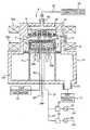
- FIG. 1shows a cross-sectional view illustrating an RIE plasma etching apparatus to which an electrode in accordance with a first preferred embodiment of the present invention is employed as an upper electrode;
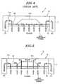
- FIG. 2describes an enlarged cross-sectional view depicting the upper electrode of the apparatus of FIG. 1 ;
- FIGS. 3A and 3Beach provide a schematic diagram showing an exemplary shape and arrangement pattern of island-shaped parts of a bond-coat layer (intermediate layer) used in the upper electrode of FIG. 2 ;
- FIG. 4represents a schematic diagram illustrating a propagation pattern of a high frequency power from a plasma, with respect to a continuous bond-coat layer (intermediate layer) between a basic material of the upper electrode and a thermally sprayed film;
- FIG. 5offers a schematic diagram depicting a propagation pattern of a high frequency power from a plasma, with respect to a bond-coat layer (intermediate layer) between a basic material of the upper electrode and a thermally sprayed film, which is composed of a plurality of island-shaped parts isolated from each other in accordance with the present invention
- FIG. 6presents a cross-sectional view schematically showing an enlarged bond-coat layer (intermediate layer) used in the upper electrode;
- FIG. 7sets forth a cross-sectional view illustrating an upper electrode including a basic material having a structure in which a base portion made of a metal and a dielectric portion are fixed to each other with screws and a thermally conductive sheet disposed therebetween;
- FIG. 8depicts a cross-sectional view describing an upper electrode including a basic material having a structure in which a base portion composed of a metal-ceramic composite material and a dielectric portion are joined with a brazing metal;
- FIGS. 9A to 9 Dshow diagrams for explaining a method for joining a base portion and a dielectric portion with an impregnated metal when the base portion is formed by impregnating a metal into a porous ceramic material.
- FIG. 1shows a cross-sectional view illustrating an RIE plasma etching apparatus employing an electrode in accordance with a first preferred embodiment of the present invention as the upper electrode.
- etching apparatusincludes a chamber (processing vessel) 1 with wall portions made of, e.g., aluminum, the chamber being sealed airtight and having a stepped cylindrical shape composed of an upper portion 1 a of a smaller diameter and a lower portion 1 b of a larger diameter.
- a supporting table 2horizontally supporting a semiconductor wafer W made of Si or the like as an object to be processed and also serving as a lower electrode.
- the supporting table 2is made of, e.g., aluminum, and supported at a conductive support 4 via an insulating plate 3 .
- a focus ring 5formed of, e.g., Si.
- a lower portion of the support 4is covered by a cover 6 .
- a baffle plate 7is provided on the outside of the support 4 , and the support 4 is connected with the chamber 1 via the cover 6 .
- the chamber 1is grounded.
- a ceiling wall portion of the chamber 1is formed as a showerhead 8 for introducing a processing gas into the chamber 1
- a bottom surface of the showerhead 8is formed as an upper electrode 9 serving as a shower plate.
- the upper electrode 9is provided opposite and parallel to the supporting table 2 serving as a lower electrode and has a plurality of gas discharge openings 10 .
- the supporting table 2i.e., the lower electrode, and the upper electrode 9 form a pair of parallel plate type electrodes.
- the upper electrode 9is grounded via the chamber 1 . Detailed configurations of the showerhead 8 and the upper electrode 9 will be described later.
- a gas exhaust port 11is formed in the bottom wall of the lower portion 1 b of the chamber 1 , and a gas exhaust unit 12 is connected to the gas exhaust port 11 . Further, by operating a vacuum pump of the gas exhaust unit 12 , an inner space of the chamber 1 can be depressurized to a specific vacuum level. Meanwhile, a loading/unloading gate 13 for a semiconductor wafer W is provided in the sidewall of the upper portion la of the chamber 1 , and the gate 13 is opened and closed by a gate valve 14 .
- a first feeder line 15is connected to the supporting table 2 , and a first matching unit 16 and first high frequency power supply 17 for forming a plasma are connected to the first feeder line 15 . Further, a high frequency power of a specific frequency of, e.g., 100 MHz, is supplied from the first high frequency power supply 17 to the supporting table 2 .
- a second feeder line 18is branched from the first feeder line 15 , and a second matching unit 19 and second high frequency power supply 20 are connected to the second feeder line 18 .
- the second high frequency power supply 20supplies a high frequency power with a specific frequency, e.g., 3.2 MHz, lower than that of the first high frequency power supply 17 , so that it overlaps with the high frequency power for forming a plasma.
- an electrostatic chuck 21for electrostatically adsorbing and maintaining a semiconductor wafer W.
- the electrostatic chuck 21is formed by interposing an electrode 21 a between insulating members 21 b , wherein a DC power supply 22 is connected to the electrode 21 a . Further, by applying a voltage from the DC power supply 22 to the electrode 21 a , the semiconductor wafer W is adsorbed by an electrostatic force, e.g., a Coulomb force.
- a coolant chamber 23is provided in the supporting table 2 , and a coolant circulates therein. That is, the coolant is introduced into the coolant chamber 23 via a coolant introducing line 23 a and discharged through a coolant discharge line 23 b . Cold heat of the coolant is thermally conducted to the semiconductor wafer W via the supporting table 2 and, accordingly, a processing surface of the semiconductor wafer W is controlled to be at a desired temperature.
- a cooling gasis introduced into a gap between the surface of the electrostatic chuck 21 and the backside of the wafer W through a gas supply line 25 by a gas introduction mechanism 24 so that the semiconductor wafer W can be effectively cooled by the coolant circulating in the coolant chamber 23 .
- the cooling gas introduced thereintocold heat of the coolant is efficiently transferred to the semiconductor wafer W, thereby improving the cooling efficiency.
- the showerhead 8has the upper electrode 9 as the shower plate having the plurality of gas discharge openings 10 in the bottom surface thereof and a gas inlet 8 a at a top surface thereof. Further, a space 26 for diffusing a gas is formed therein.
- a gas supply line 27is connected to the gas inlet 8 a , and a processing gas supply system 28 for supplying a processing gas is connected to the other end portion of the gas supply line 27 .
- a highly corrosive gas containing halogen elementsuch as fluorine (F) or chlorine (Cl) is used.
- processing gas supplied from the processing gas supply system 28reaches the space 26 of the showerhead 8 via the gas supply line 27 and the gas inlet 8 a and is then discharged from the gas discharge openings 10 .
- multi-pole ring magnets 29 a and 29 bare disposed around the periphery of the upper portion la of the chamber 1 such that the gate 13 is interposed therebetween.
- the multi-pole ring magnets 29 a and 29 bare formed by attaching a plurality of columnar anisotropic segment magnets to a ring-shaped case made of a magnetic material, wherein magnetic pole orientations between the adjacent multiple columnar segment magnets are opposite from each other. Accordingly, magnetic force lines are formed between the adjacent segment magnets, so that a magnetic field is formed only at a peripheral portion of a processing space between the upper and lower electrodes, thereby confining a plasma in the processing space.
- the upper electrode 9is configured by sequentially forming a bond-coat layer 32 as a metallic intermediate layer and a thermally sprayed film 33 made of an insulating ceramic on the bottom surface, i.e., a surface of a basic material 31 .
- the basic material 31has a base portion 31 a made of a conductive material such as Al, Si or the like and a dielectric portion 31 b interposed in the central portion of the base portion to include the mid section of the bottom surface.
- the dielectric portion 31 bprovides the functions as described below.
- the dielectric portion 31 bemploys a material having a relatively high dielectric constant, e.g., alumina (Al 2 O 3 ), aluminum nitride (AlN), silicon nitride (Si 3 N 4 ), silica (SiO 2 ), yttrium oxide (Y 2 O 3 ) or the like.
- aluminaAl 2 O 3
- AlNaluminum nitride
- Si 3 N 4silicon nitride
- silicaSiO 2
- Y 2 O 3yttrium oxide
- the base portion 31 a and the dielectric portion 31 b forming the basic material 31are joined together by using, e.g., screws.
- a thermally conductive sheete.g., a silicon rubber, therebetween.
- the thermally sprayed film 33needs to be formed of an insulating ceramic having a high plasma resistance, e.g., alumina (Al 2 O 3 ) or yttrium oxide (Y 2 O 3 ).
- an insulating ceramic having a high plasma resistancee.g., alumina (Al 2 O 3 ) or yttrium oxide (Y 2 O 3 ).
- the bond-coat layer 32is formed for improving adhesiveness of the thermally sprayed film 33 , and preferably made of a soft metal such as aluminum (Al) or nickel (Ni).
- the bond-coat layer 32is comprised of a plurality of island-shaped parts 32 a isolated from each other.
- a method for forming the bond-coat layer 21is not particularly limited. However, it is preferable to employ a thermal spraying method using a mask. With such method, it is possible to form the multiple island-shaped parts 32 a isolated from each other relatively easily.
- shapes of the island-shaped parts 32 a forming the bond-coat layer 32are not particularly limited, they are preferable to have a shape that they can be arranged with ease in a regular pattern. For example, they may have a circular shape shown in FIG. 3A or a square shape illustrated in FIG. 3B .
- a semiconductor wafer Wis loaded into the chamber 1 through the gate 13 by opening the gate valve 14 and, then, mounted on the supporting table 2 .
- the inner space of the chamber 1is vacuum pumped through the gas exhaust port 11 by a vacuum pump of the gas exhaust unit 12 .
- a high frequency power of, e.g., 100 MHz, for forming a plasmais supplied from the first high frequency power supply 17 to the supporting table 2 .
- a high frequency power electric fieldis formed between the upper electrode 9 and the supporting table 1 serving as a lower electrode.
- a high frequency power of, e.g., 3.2 MHz, for attracting ionsis supplied from the second high frequency power supply 30 to the supporting table 2 overlaping with the plasma-forming high frequency power supply from the first high frequency power supply 17 .
- the semiconductor wafer Wis adsorptively held on the electrostatic chuck 21 by a specific voltage applied from the DC power supply 22 to the electrode 21 a of the electrostatic chuck 21 , e.g., by the Coulomb force.
- a high frequency plasma of the processing gasis formed in a processing space between the upper electrode 9 and the supporting table 2 serving as a lower electrode, and then, a specific film of the semiconductor wafer W is etched.
- a high frequency power from the plasma formed in the processing spacereaches the upper electrode 9 and, then, flows into a ground via the wall portions of the chamber 1 .
- a continuous bond-coat layer 32 ′is interposed between the basic material 31 and the thermally sprayed film 33 .
- the bond-coat layer 32 ′becomes a passageway for a high frequency power
- the high frequency power from the plasmaflows through the bond-coat layer 32 ′ into the ground. Accordingly, the conventional case behaves as if the dielectric portion 31 b is not present with respect to the plasma, so that the intended effect of the dielectric portion 31 b , which is to decrease the high frequency power, is not effectively obtained.
- the bond-coat layer 32i.e., the metallic intermediate layer, is comprised of the multiple island-shaped parts 32 a , which are isolated from each other.
- the bond-coat layer 32since the high frequency power can be blocked off between the island-shaped parts 32 a , the high frequency power flows through the basic material 31 , but not the bond-coat layer 32 . Therefore, the effect of the dielectric portion 31 b of the basic material 31 , which is capable of decreasing the high frequency power, is effectively maintained.
- island-shaped part 32 aIn addition, if the area of island-shaped part 32 a is made excessively large, electric charges stored in a single island-shaped part would increase, so that an unexpected discharge could occur. From such point of view, it is preferable to minimize the area of the island-shaped part 32 a . However, if the area thereof is made excessively small, the total area of the bond-coat portion becomes small, thereby deteriorating the adhesiveness thereof. Therefore, it is necessary to set an optimal area considering this issue.
- the distance (gap) a between the island-shaped parts 32 ais preferably about 0.1 mm to 0.2 mm.
- the length b of one sideis preferably about 0.7 mm.
- the thickness c of the bond-coat layer 32 shown in FIG. 6becomes thick, the final thermally sprayed surface becomes less flat, the surface being formed after the thermally sprayed film 33 is formed. Accordingly, the thickness is preferable to be as thin as possible. However, if it is too thin, the effect of improving its adhesiveness is reduced. Hence, the thickness c of the bond-coat layer 32 is preferably about 0.03 to 0.05 mm.
- the base portion 31 amade of a metal such as Al or the like and the dielectric portion 31 b are joined together by using screws 34 with the thermally conductive sheet 35 interposed therebetween.
- the basic material 31 of the upper electrode 9is composed of a base portion 31 a ′ (made of a metal-ceramic composite material) and a dielectric portion 31 b ′, wherein they are joined together by a brazing metal 37 . Further, the sleeve 38 made of a dielectric material is provided around the gas discharge openings 10 . Furthermore, the bond-coat layer 32 and the thermally sprayed film 33 are formed in the same manner as in the aforementioned embodiment.
- the base portion 31 a ′ composed of the metal-ceramic composite material forming the basic material 31has both a high conductivity of metal and a low thermal expansibility of ceramic.
- a thermal expansion discrepancy between the base portion 31 a ′ and the dielectric portion 31 bis small, so that a mechanical imprecision therebetween can be significantly eliminated.
- the thermal expansion discrepancy therebetweenis small, defects such as fine cracks in the thermal spraying process rarely occur.
- the mechanical imprecision caused by he thermal expansion discrepancycan be reduced, they can be joined to each other by the brazing metal 37 without screws.
- the gap between the base portion 31 a ′ and the dielectric portion 31 bcan be sealed therewith, preventing a thermal resistance resulting from the leakage of introduction gas or the gap. Moreover, since there is no gap at the interface of the base portion 31 a ′ and the dielectric portion 31 b , no gap is present on the thermally sprayed film 33 formed on the entire basic material surface. Besides, the metal-ceramic composite material has a high thermal conductivity, so that a nonuniformity of temperature rarely occurs on the upper electrode 9 . If the dielectric portion 31 b employs a material having a high thermal conductivity, particularly AlN, the entire basic material 31 can have an extremely high thermal conductivity. Accordingly, a temperature distribution of the upper electrode 9 can be further uniformized.
- the brazing metal 37can be protected from a plasma coming in through the gas discharge openings 10 , so that the chamber atmosphere can be prevented from being contaminated by the brazing metal 37 scattered by the plasma.
- a material of the sleeve 38is preferably a high purity material having a high stability against the plasma. The material also needs to have an affinity for the brazing metal. Accordingly, as the sleeve 38 , it is preferable to use a dielectric material identical to that of the dielectric portion 31 b.
- the metal-ceramic composite materialit is possible to appropriately employ a material formed by impregnating a metal into a porous ceramic and compressing it.
- a porous ceramicAl 2 O 3 , SiO 2 or the like can be used.
- the metalAl, Ni or the like can be used. Since, however, Al has a low melting point, if the brazing metal has a higher melting point than Al, Al would melt during the brazing process, which limits its application as a result.
- the base portion 31 a ′ made of the metal-ceramic composite material and the dielectric portion 31 bare joined together by using the brazing metal 34 .
- the base portion 31 a ′is formed by impregnating the metal into a porous ceramic, the base portion 31 a ′ and the dielectric portion 31 b may be adhered to each other by filling the gap therebetween with the impregnated metal.
- the dielectric portion 31 bis provided at the porous ceramic 41 that is a precursor of the base portion 31 a ′ with a uniform gap provided by spacers 42 therebetween (see FIG. 9A ).
- the sleeve 38is provided in advance (not illustrated in FIGS. 9A to 9 B).
- a molten metalis pressurized by a gas pressure or the like and then impregnated into the porous ceramic 41 (see FIG. 9B ).
- a space between a porous ceramic 41 ′ and the dielectric portion 31 bis sealed with the molten metal and then becomes a junction layer 43 (see FIG. 9C ) .
- the basic material 31 composed of the base portion 31 a ′ and the dielectric portion 31 bis obtained with the junction layer 43 made of the impregnated metal (see FIG. 9D ).
- the base portion 31 a ′ and the dielectric portion 31 bcan be joined together without using the brazing metal while the metal is impregnated, so that the process becomes simplified and the impregnated metal can be selected without regard to its melting point. Accordingly, in comparison with a case using the brazing metal, the choice of impregnated metal is not as limited, therefore, Al having a low melting point can be used as a impregnated metal.
- the present inventioncan be varied without being limited to the aforementioned embodiments.
- the present inventionmay be applied to the upper electrode of the RIE plasma etching apparatus.
- the present inventionmay be applied to any electrode as long as it is used under the condition that a high frequency power from a high frequency plasma is supplied thereto in a parallel plate type plasma processing apparatus.
- the present inventionmay be applied to a thermally sprayed member used under a condition where the high frequency power from the high frequency plasma is supplied thereto and it is required to prevent the high frequency power from flowing through a metallic intermediate layer serving as a bond-coat layer.
Landscapes
- Chemical & Material Sciences (AREA)
- Engineering & Computer Science (AREA)
- Organic Chemistry (AREA)
- Inorganic Chemistry (AREA)
- Chemical Kinetics & Catalysis (AREA)
- Materials Engineering (AREA)
- Mechanical Engineering (AREA)
- Metallurgy (AREA)
- Physics & Mathematics (AREA)
- Plasma & Fusion (AREA)
- Analytical Chemistry (AREA)
- Ceramic Engineering (AREA)
- Plasma Technology (AREA)
- Drying Of Semiconductors (AREA)
- Cleaning In General (AREA)
- Coating By Spraying Or Casting (AREA)
Abstract
Description
- The present invention relates to a thermally sprayed member used in a chamber of a plasma processing apparatus, an electrode for generating a plasma and a plasma processing apparatus using such electrode.
- In manufacturing a semiconductor, liquid crystal device or the like, a plasma processing which employs a plasma has been widely used. In such plasma processing, for components like an electrode exposed to a plasma atmosphere in a chamber, it has been proposed to employ a thermally sprayed film formed on the surface of a basic material of an insulting ceramic with a high corrosion resistance such as alumina (Al2O3), yttrium oxide (Y2O3) or the like, so that they can be resistant to the plasma. (see, e.g.,
page 3, FIG. 2 of Japanese Patent Laid-open Publication No. H9-339895). - When such thermally sprayed films of alumina, yttrium oxide or the like are formed on a basic nonmetal material like ceramic or quartz, if the thermal spraying is carried out by only performing a beads blast, chemical blast or the like on the surface thereof as when a metal basic material is used, because a dielectric-material component has a low tolerance to a hardening shrinkage of the thermally sprayed film, the anchoring effect of the thermally sprayed film deteriorates. As a result, the thermally sprayed film is readily stripped off. In order to eliminate this problem, there has been proposed a method for thermally spraying a soft-metal thin film. such as aluminum (Al), nickel (Ni) or the like as an intermediate layer between the basic material and the thermally sprayed film to enhance the anchor therebetween (see, e.g., Japanese Patent Laid-open Publication No. H9-69554).
- As for the field of plasma processing, a parallel plate type plasma processing apparatus to form a high frequency electric field between a pair of electrodes disposed vertically facing each other has been widely used. In order to generate a high-density plasma by using such apparatus, the applied frequency needs to be increased. However, when the applied frequency is increased as such, not only does the electric field distribution on the electrode surface becomes nonuniform, but also the plasma density becomes nonuniform as well. Therefore, there has been suggested a method for uniformizing the plasma density by providing a dielectric member such as a ceramic or the like at, e.g., the central portion of an exposed surface of an upper electrode so that the electric field distribution is uniformized (see, e.g., Japanese Patent Laid-open Publication No. 2000-323456).
- When the thermally sprayed film is formed on a basic material of the electrode having a dielectric member on the surface thereof, if an intermediate layer (bond-coat layer) is formed as described above, the bond-coat layer itself, which is metal, becomes a conductive layer for a high frequency power. Therefore, the dielectric member, which is intended to obstruct the penetration of a high frequency power, is not able to function as expected.
- It is, therefore, an object of the present invention to provide a thermally sprayed component and electrode having a metallic intermediate layer provided between a basic material and a thermally sprayed film wherein the intermediate layer would not allow a high frequency power to penetrate, and a plasma processing apparatus using such an electrode.
- In accordance with one aspect of the invention, there is provided a thermally sprayed member including: a basic material in which at least a part of a surface thereof is made of a dielectric material; a thermally sprayed film formed on the surface of the basic material, the thermally sprayed film being made of an insulating ceramic; and an intermediate layer made of a metal, provided between the basic material and the thermally sprayed film, for increasing a bonding force therebetween, wherein the intermediate layer is composed of a plurality of island-shaped parts separated from each other in a thermally sprayed member in which a thermally sprayed film forming portion thereof is exposed to a high frequency plasma atmosphere.
- In accordance with another aspect of the invention, there is provided an electrode including: a basic material including a base portion made of a conductive material and a dielectric portion having a part of a surface of the basic material; a thermally sprayed film provided on the surface of the basic material, the thermally sprayed film being made of an insulating ceramic; and an intermediate layer made of a metal, provided between the basic material and the thermally sprayed film, for increasing a bonding force therebetween, wherein the intermediate layer is composed of a plurality of island-shaped parts separated from each other in an electrode for forming a high frequency plasma on the thermally sprayed film side.
- In accordance with still another aspect of the invention, there is provided a plasma processing apparatus for performing a specific plasma process on a substrate to be processed by using a plasma, the apparatus including: a chamber maintained under a decompressed atmosphere, for accommodating therein an object to be processed; a first and a second electrode opposedly provided in the chamber; and a plasma generating unit for generating a plasma of the processing gas by forming a high frequency electric field between the first and the second electrode, wherein at least one of the first and the second electrode includes a basic material having a base portion made of a conductive material and a dielectric portion including a part of a surface of the basic material; a thermally sprayed film provided on the surface of the basic material, the thermally sprayed film being made of an insulating ceramic; and an intermediate layer provided between the basic material and the thermally sprayed film for increasing an adhesivity therebetween, the intermediate layer being formed of a metal and composed of a plurality of island-shaped parts separated from each other.
- In accordance with the present invention, since the metallic intermediate layer, which lies between the basic material and the thermally sprayed film, is comprised of a plurality of island-shaped parts isolated from each other, a high frequency current can be blocked off between the island-shaped parts. Therefore, when a high frequency plasma is discharged on the side of the thermally sprayed film, it is prevented from penetrating the intermediate layer. Accordingly, when an electrode in which a thermally sprayed film made of an insulating ceramic is formed on the surface of a basic material having a base portion (made of a conductive material) and a dielectric portion (partially including the surface of the basic material) via the intermediate layer made of a metal, the high frequency power cannot penetrate the intermediate layer. Therefore, the intended function of the dielectric material portion can be effectively maintained.
- In the present invention, it is preferable that a gap between the adjacent island-shaped parts of the intermediate layer is smaller than the skin depth of the high frequency power for generating a plasma. Accordingly, it is possible to ensure that the intermediate layer blocks off the high frequency power.
- In the electrode, the base portion made of a conductive material forming a basic material can be made of a metal or metal-ceramic composite material. In case the base portion is made of a metal-ceramic composite material, since its thermal expansion coefficient is smaller than that of metal, it is possible to reduce the discrepancy of thermal expansion between the base portion and the dielectric portion. Ultimately, this almost eliminates the mechanical imprecision between the portions. Further; only a small discrepancy in thermal expansion also helps to minimize defects such as fine cracks in the thermal spraying treatment. Moreover, since the mechanical defects from thermal expansion discrepancy are kept minimal, it is possible to bond the base portion and the dielectric portion with a brazing metal. By using the brazing metal to bond them, any gaps between the base portion and the dielectric material can be sealed, thereby preventing gas leakage or thermal resistance from the gaps. Furthermore, no gap is formed on the thermally sprayed film covering the entire surface of the basic material.
- When the base portion made of a basic material is formed of a metal-ceramic composite material, it is preferable to impregnate metal into a porous ceramic material. Further, when a metal-ceramic composite material is used, it is possible to join the base portion and the dielectric portion by charging therebetween the metal impregnated into the base portion. As a result, in addition to any effects from using brazing metal as a joint, the process becomes simplified. Further, although a metal having a lower melting point than that of the brazing metal is used as impregnating metal, the same effects of using a brazing metal are obtained.
- Further, the above electrode may have a plurality of gas discharge openings penetrating the basic material, intermediate layer and thermally sprayed film, wherein sleeves made of a dielectric material are provided around the respective gas discharge openings. Accordingly, even through the inner walls of the gas discharge openings have a low plasma resistance, they are protected by the sleeve.
- As for the plasma processing apparatus, it is possible to employ a plasma processing apparatus in which the first and the second electrode, respectively serving as an upper and a lower electrode, are vertically disposed opposite to each other, and the plasma generating unit has a high frequency power supply for applying a high frequency power to the second electrode on which an object to be processed is mounted, wherein the first electrode has the configuration of the present invention.
- In such a plasma processing apparatus, the processing gas inlet unit has a showerhead for discharging gas from a plurality of openings, and the first electrode serving as a shower plate of the bottom surface of the showerhead has a plurality of gas discharge openings.
- In accordance with the present invention, a high frequency current can be blocked off between the island-shaped parts forming the intermediate layer, which are isolated from each other. Therefore, in case a high frequency plasma is discharged on the side of the thermally sprayed film, a high frequency power can be prevented from flowing through the intermediate layer.
- The above and other objects and features of the present invention will become apparent from the following description of preferred embodiments, given in conjunction with the accompanying drawings, in which:
FIG. 1 shows a cross-sectional view illustrating an RIE plasma etching apparatus to which an electrode in accordance with a first preferred embodiment of the present invention is employed as an upper electrode;FIG. 2 describes an enlarged cross-sectional view depicting the upper electrode of the apparatus ofFIG. 1 ;FIGS. 3A and 3B each provide a schematic diagram showing an exemplary shape and arrangement pattern of island-shaped parts of a bond-coat layer (intermediate layer) used in the upper electrode ofFIG. 2 ;FIG. 4 represents a schematic diagram illustrating a propagation pattern of a high frequency power from a plasma, with respect to a continuous bond-coat layer (intermediate layer) between a basic material of the upper electrode and a thermally sprayed film;FIG. 5 offers a schematic diagram depicting a propagation pattern of a high frequency power from a plasma, with respect to a bond-coat layer (intermediate layer) between a basic material of the upper electrode and a thermally sprayed film, which is composed of a plurality of island-shaped parts isolated from each other in accordance with the present invention;FIG. 6 presents a cross-sectional view schematically showing an enlarged bond-coat layer (intermediate layer) used in the upper electrode;FIG. 7 sets forth a cross-sectional view illustrating an upper electrode including a basic material having a structure in which a base portion made of a metal and a dielectric portion are fixed to each other with screws and a thermally conductive sheet disposed therebetween;FIG. 8 depicts a cross-sectional view describing an upper electrode including a basic material having a structure in which a base portion composed of a metal-ceramic composite material and a dielectric portion are joined with a brazing metal; andFIGS. 9A to9D show diagrams for explaining a method for joining a base portion and a dielectric portion with an impregnated metal when the base portion is formed by impregnating a metal into a porous ceramic material.- Hereinafter, preferred embodiments of the present invention will be described in detail with reference to the accompanying drawings.
FIG. 1 shows a cross-sectional view illustrating an RIE plasma etching apparatus employing an electrode in accordance with a first preferred embodiment of the present invention as the upper electrode. Such etching apparatus includes a chamber (processing vessel)1 with wall portions made of, e.g., aluminum, the chamber being sealed airtight and having a stepped cylindrical shape composed of an upper portion1aof a smaller diameter and a lower portion1bof a larger diameter.- Installed in the
chamber 1 is a supporting table2 horizontally supporting a semiconductor wafer W made of Si or the like as an object to be processed and also serving as a lower electrode. The supporting table2 is made of, e.g., aluminum, and supported at a conductive support4 via aninsulating plate 3. Further, installed around the upper periphery of the insulatingplate 3 is afocus ring 5 formed of, e.g., Si. A lower portion of the support4 is covered by acover 6. Further, abaffle plate 7 is provided on the outside of the support4, and the support4 is connected with thechamber 1 via thecover 6. Thechamber 1 is grounded. - A ceiling wall portion of the
chamber 1 is formed as ashowerhead 8 for introducing a processing gas into thechamber 1, and a bottom surface of theshowerhead 8 is formed as anupper electrode 9 serving as a shower plate. Theupper electrode 9 is provided opposite and parallel to the supporting table2 serving as a lower electrode and has a plurality ofgas discharge openings 10. In other words, the supporting table2, i.e., the lower electrode, and theupper electrode 9 form a pair of parallel plate type electrodes. Further, theupper electrode 9 is grounded via thechamber 1. Detailed configurations of theshowerhead 8 and theupper electrode 9 will be described later. - A
gas exhaust port 11 is formed in the bottom wall of the lower portion1bof thechamber 1, and agas exhaust unit 12 is connected to thegas exhaust port 11. Further, by operating a vacuum pump of thegas exhaust unit 12, an inner space of thechamber 1 can be depressurized to a specific vacuum level. Meanwhile, a loading/unloading gate 13 for a semiconductor wafer W is provided in the sidewall of the upper portion la of thechamber 1, and thegate 13 is opened and closed by agate valve 14. - A
first feeder line 15 is connected to the supporting table2, and afirst matching unit 16 and first highfrequency power supply 17 for forming a plasma are connected to thefirst feeder line 15. Further, a high frequency power of a specific frequency of, e.g., 100 MHz, is supplied from the first highfrequency power supply 17 to the supporting table2. - A
second feeder line 18 is branched from thefirst feeder line 15, and asecond matching unit 19 and second highfrequency power supply 20 are connected to thesecond feeder line 18. The second highfrequency power supply 20 supplies a high frequency power with a specific frequency, e.g., 3.2 MHz, lower than that of the first highfrequency power supply 17, so that it overlaps with the high frequency power for forming a plasma. - Installed on the surface of the supporting table2 is an
electrostatic chuck 21 for electrostatically adsorbing and maintaining a semiconductor wafer W. Theelectrostatic chuck 21 is formed by interposing anelectrode 21abetween insulatingmembers 21b, wherein aDC power supply 22 is connected to theelectrode 21a. Further, by applying a voltage from theDC power supply 22 to theelectrode 21a, the semiconductor wafer W is adsorbed by an electrostatic force, e.g., a Coulomb force. - A
coolant chamber 23 is provided in the supporting table2, and a coolant circulates therein. That is, the coolant is introduced into thecoolant chamber 23 via acoolant introducing line 23aand discharged through acoolant discharge line 23b. Cold heat of the coolant is thermally conducted to the semiconductor wafer W via the supporting table2 and, accordingly, a processing surface of the semiconductor wafer W is controlled to be at a desired temperature. - Moreover, although the
chamber 1 is vacuum pumped by thegas exhaust unit 12 and then maintained at a vacuum, a cooling gas is introduced into a gap between the surface of theelectrostatic chuck 21 and the backside of the wafer W through agas supply line 25 by agas introduction mechanism 24 so that the semiconductor wafer W can be effectively cooled by the coolant circulating in thecoolant chamber 23. With the cooling gas introduced thereinto, cold heat of the coolant is efficiently transferred to the semiconductor wafer W, thereby improving the cooling efficiency. - As described above, the
showerhead 8 has theupper electrode 9 as the shower plate having the plurality ofgas discharge openings 10 in the bottom surface thereof and agas inlet 8aat a top surface thereof. Further, aspace 26 for diffusing a gas is formed therein. Agas supply line 27 is connected to thegas inlet 8a, and a processinggas supply system 28 for supplying a processing gas is connected to the other end portion of thegas supply line 27. - As for a processing gas, a highly corrosive gas containing halogen element such as fluorine (F) or chlorine (Cl) is used. Such processing gas supplied from the processing
gas supply system 28 reaches thespace 26 of theshowerhead 8 via thegas supply line 27 and thegas inlet 8aand is then discharged from thegas discharge openings 10. - In the meantime, two
multi-pole ring magnets chamber 1 such that thegate 13 is interposed therebetween. Themulti-pole ring magnets - Hereinafter, configurations of the
upper electrode 9 will be described in detail. - As shown in
FIG. 2 illustrating an enlarged cross sectional view of theupper electrode 9, theupper electrode 9 is configured by sequentially forming a bond-coat layer 32 as a metallic intermediate layer and a thermally sprayedfilm 33 made of an insulating ceramic on the bottom surface, i.e., a surface of abasic material 31. - The
basic material 31 has abase portion 31amade of a conductive material such as Al, Si or the like and adielectric portion 31binterposed in the central portion of the base portion to include the mid section of the bottom surface. Thedielectric portion 31bprovides the functions as described below. - To elaborate, when a basic material of an electrode is entirely formed of a conductor, the central position of the bottom surface of the electrode is exposed to a plasma and it becomes an exposed end in an RF equivalent circuit. As a result, a distribution of electric field supplied to a plasma becomes a standing wave type, which results in a nonuniform plasma density. Such tendency becomes markedly widespread as the frequency of a high frequency power is raised to form a high-density plasma. To that end, by providing a dielectric portion at the central portion, the high frequency power is reduced at such portion and the strength of an electric field at the bottom central portion of the
electrode 9 is also decreased. As a result, the strength of the electric field at the bottom surface of the electrode becomes uniform, thereby uniformizing the plasma density. - From such point of view, the
dielectric portion 31bemploys a material having a relatively high dielectric constant, e.g., alumina (Al2O3), aluminum nitride (AlN), silicon nitride (Si3N4), silica (SiO2), yttrium oxide (Y2O3) or the like. - The
base portion 31aand thedielectric portion 31bforming thebasic material 31 are joined together by using, e.g., screws. In this case, it is preferable to provide a thermally conductive sheet, e.g., a silicon rubber, therebetween. - The thermally sprayed
film 33 needs to be formed of an insulating ceramic having a high plasma resistance, e.g., alumina (Al2O3) or yttrium oxide (Y2O3). - The bond-
coat layer 32 is formed for improving adhesiveness of the thermally sprayedfilm 33, and preferably made of a soft metal such as aluminum (Al) or nickel (Ni). The bond-coat layer 32 is comprised of a plurality of island-shapedparts 32aisolated from each other. A method for forming the bond-coat layer 21 is not particularly limited. However, it is preferable to employ a thermal spraying method using a mask. With such method, it is possible to form the multiple island-shapedparts 32aisolated from each other relatively easily. - Although shapes of the island-shaped
parts 32aforming the bond-coat layer 32 are not particularly limited, they are preferable to have a shape that they can be arranged with ease in a regular pattern. For example, they may have a circular shape shown inFIG. 3A or a square shape illustrated inFIG. 3B . - In such configured plasma etching apparatus, first, a semiconductor wafer W is loaded into the
chamber 1 through thegate 13 by opening thegate valve 14 and, then, mounted on the supporting table2. Next, the inner space of thechamber 1 is vacuum pumped through thegas exhaust port 11 by a vacuum pump of thegas exhaust unit 12. - Further, in a condition where a processing gas is introduced at a specific flow rate from the processing
gas supply system 28 into thechamber 1 and a gas pressure in thechamber 1 is set at, e.g., 13 Pa to 1333 Pa (100 mTorr to 10 Torr), a high frequency power of, e.g., 100 MHz, for forming a plasma is supplied from the first highfrequency power supply 17 to the supporting table2. As a result, a high frequency power electric field is formed between theupper electrode 9 and the supporting table1 serving as a lower electrode. Furthermore, a high frequency power of, e.g., 3.2 MHz, for attracting ions is supplied from the second high frequency power supply30 to the supporting table2 overlaping with the plasma-forming high frequency power supply from the first highfrequency power supply 17. At this time, the semiconductor wafer W is adsorptively held on theelectrostatic chuck 21 by a specific voltage applied from theDC power supply 22 to theelectrode 21aof theelectrostatic chuck 21, e.g., by the Coulomb force. - In such state, a high frequency plasma of the processing gas is formed in a processing space between the
upper electrode 9 and the supporting table2 serving as a lower electrode, and then, a specific film of the semiconductor wafer W is etched. - At this time, a high frequency power from the plasma formed in the processing space reaches the
upper electrode 9 and, then, flows into a ground via the wall portions of thechamber 1. However, in a conventional case, as illustrated inFIG. 4 , a continuous bond-coat layer 32′ is interposed between thebasic material 31 and the thermally sprayedfilm 33. In that case, since the bond-coat layer 32′ becomes a passageway for a high frequency power, the high frequency power from the plasma flows through the bond-coat layer 32′ into the ground. Accordingly, the conventional case behaves as if thedielectric portion 31bis not present with respect to the plasma, so that the intended effect of thedielectric portion 31b, which is to decrease the high frequency power, is not effectively obtained. - To that end, in this embodiment, the bond-
coat layer 32, i.e., the metallic intermediate layer, is comprised of the multiple island-shapedparts 32a, which are isolated from each other. As illustrated inFIG. 5 , since the high frequency power can be blocked off between the island-shapedparts 32a, the high frequency power flows through thebasic material 31, but not the bond-coat layer 32. Therefore, the effect of thedielectric portion 31bof thebasic material 31, which is capable of decreasing the high frequency power, is effectively maintained. - A minimum distance (gap) a (see
FIGS. 2 and 3 ) between adjacent island-shapedparts 32aforming the bond-coat layer 32 is determined according to the skin depth of the frequency of a high frequency power applied thereto. To elaborate, the high frequency power flows through the surface portion of the conductor portion, and the thickness of such portion becomes the skin depth. Further, if the distance (gap) a between adjacent island-shapedparts 32ais greater than the skin depth, the high frequency power is not conducted. However, the capacity for blocking a high frequency power and the adhesiveness of the bond-coat layer 32 are in a reciprocal relationship and, therefore, if the distance between the adjacent island-shapedparts 32ais set to be too far, the adhesiveness would deteriorate. Moreover, the skin depth δ is defined by an equation of δ=(2/ωσμ)1/2(wherein, ω=2πf (f: frequency), σ: conductivity, μ: magnetic permeability) - In addition, if the area of island-shaped
part 32ais made excessively large, electric charges stored in a single island-shaped part would increase, so that an unexpected discharge could occur. From such point of view, it is preferable to minimize the area of the island-shapedpart 32a. However, if the area thereof is made excessively small, the total area of the bond-coat portion becomes small, thereby deteriorating the adhesiveness thereof. Therefore, it is necessary to set an optimal area considering this issue. - For example, when the frequency of the high frequency power for forming a plasma is 1000 MHz, the distance (gap) a between the island-shaped
parts 32ais preferably about 0.1 mm to 0.2 mm. Further, in case the island-shapedparts 32ahave a square shape as shown inFIG. 3B , the length b of one side is preferably about 0.7 mm. - Further, if the thickness c of the bond-
coat layer 32 shown inFIG. 6 becomes thick, the final thermally sprayed surface becomes less flat, the surface being formed after the thermally sprayedfilm 33 is formed. Accordingly, the thickness is preferable to be as thin as possible. However, if it is too thin, the effect of improving its adhesiveness is reduced. Hence, the thickness c of the bond-coat layer 32 is preferably about 0.03 to 0.05 mm. - Hereinafter, another embodiment of a structure of the upper electrode will be described.
- In the aforementioned
upper electrode 9, as illustrated inFIG. 7 , as thebasic material 31, thebase portion 31amade of a metal such as Al or the like and thedielectric portion 31bare joined together by usingscrews 34 with the thermallyconductive sheet 35 interposed therebetween. In such case, the following problems exist: - 1. Since a thermal expansion coefficient of a metal forming the
base portion 31ais greater than that of a dielectric material of thedielectric portion 31b, a mechanical imprecision is likely to occur between the base and dielectric portions under a high temperature condition. - 2. When the base portion and dielectric portions are joined by screws, to avoid a possible breakage thereof, a large torque cannot be applied to the screws. As a result, an introduction gas may leak and a dimensional or attachment imprecision may result. Although this error can be diminished by using a thermally conductive sheet such as a silicon rubber or the like, it cannot be fully eliminated. So the thermally conductive sheet may rather deteriorate with time while being used in a high temperature condition. Further, since the thermally conductive sheet has a low resistance against a plasma from the gas discharge openings and is likely to have a low thermal resistance, a thermal shock fracture of the dielectric portion tends to be common. The uniformity of surface temperature distribution is also adversely affected as a result.
- 3. In case the
base portion 31aand thedielectric portion 31bare joined together by screws, gaps form therebetween and hence on the thermally sprayed surface as well. As a result, a plasma resistance or an abnormal discharge can occur at such portions. - To deal with the issues above, here, as illustrated in
FIG. 8 , thebasic material 31 of theupper electrode 9 is composed of abase portion 31a′ (made of a metal-ceramic composite material) and adielectric portion 31b′, wherein they are joined together by abrazing metal 37. Further, thesleeve 38 made of a dielectric material is provided around thegas discharge openings 10. Furthermore, the bond-coat layer 32 and the thermally sprayedfilm 33 are formed in the same manner as in the aforementioned embodiment. - The
base portion 31a′ composed of the metal-ceramic composite material forming thebasic material 31 has both a high conductivity of metal and a low thermal expansibility of ceramic. Thus, even at a high temperature, a thermal expansion discrepancy between thebase portion 31a′ and thedielectric portion 31bis small, so that a mechanical imprecision therebetween can be significantly eliminated. Further, since the thermal expansion discrepancy therebetween is small, defects such as fine cracks in the thermal spraying process rarely occur. Furthermore, since the mechanical imprecision caused by he thermal expansion discrepancy can be reduced, they can be joined to each other by the brazingmetal 37 without screws. As described above, by using thebrazing metal 37, the gap between thebase portion 31a′ and thedielectric portion 31bcan be sealed therewith, preventing a thermal resistance resulting from the leakage of introduction gas or the gap. Moreover, since there is no gap at the interface of thebase portion 31a′ and thedielectric portion 31b, no gap is present on the thermally sprayedfilm 33 formed on the entire basic material surface. Besides, the metal-ceramic composite material has a high thermal conductivity, so that a nonuniformity of temperature rarely occurs on theupper electrode 9. If thedielectric portion 31bemploys a material having a high thermal conductivity, particularly AlN, the entirebasic material 31 can have an extremely high thermal conductivity. Accordingly, a temperature distribution of theupper electrode 9 can be further uniformized. - In addition, by providing the
sleeve 38 made of a dielectric material around thegas discharge openings 10, thebrazing metal 37 can be protected from a plasma coming in through thegas discharge openings 10, so that the chamber atmosphere can be prevented from being contaminated by the brazingmetal 37 scattered by the plasma. A material of thesleeve 38 is preferably a high purity material having a high stability against the plasma. The material also needs to have an affinity for the brazing metal. Accordingly, as thesleeve 38, it is preferable to use a dielectric material identical to that of thedielectric portion 31b. - As for the metal-ceramic composite material, it is possible to appropriately employ a material formed by impregnating a metal into a porous ceramic and compressing it. As for the porous ceramic, Al2O3, SiO2or the like can be used. As for the metal, Al, Ni or the like can be used. Since, however, Al has a low melting point, if the brazing metal has a higher melting point than Al, Al would melt during the brazing process, which limits its application as a result.
- In this case, it is preferable to perform the brazing adhesion during a process for impregnating a metal into a porous dielectric material. Accordingly, it is possible to completely seal any gaps between the
base portion 31a′ and thedielectric portion 31b. - There has been described in the above example that the
base portion 31a′ made of the metal-ceramic composite material and thedielectric portion 31bare joined together by using thebrazing metal 34. However, while thebase portion 31a′ is formed by impregnating the metal into a porous ceramic, thebase portion 31a′ and thedielectric portion 31bmay be adhered to each other by filling the gap therebetween with the impregnated metal. - Hereinafter, a method therefor will be described in detail with reference to
FIG. 9 . - First, the
dielectric portion 31bis provided at the porous ceramic41 that is a precursor of thebase portion 31a′ with a uniform gap provided byspacers 42 therebetween (seeFIG. 9A ). At this time, thesleeve 38 is provided in advance (not illustrated inFIGS. 9A to9B). Next, a molten metal is pressurized by a gas pressure or the like and then impregnated into the porous ceramic41 (seeFIG. 9B ). By keeping the pressurization of the molten metal even after the molten metal spread throughout the porous ceramic41, a space between a porous ceramic41′ and thedielectric portion 31bis sealed with the molten metal and then becomes a junction layer43 (seeFIG. 9C ) . Thereafter, by cooling them, thebasic material 31 composed of thebase portion 31a′ and thedielectric portion 31bis obtained with thejunction layer 43 made of the impregnated metal (seeFIG. 9D ). - By employing such method, the
base portion 31a′ and thedielectric portion 31bcan be joined together without using the brazing metal while the metal is impregnated, so that the process becomes simplified and the impregnated metal can be selected without regard to its melting point. Accordingly, in comparison with a case using the brazing metal, the choice of impregnated metal is not as limited, therefore, Al having a low melting point can be used as a impregnated metal. - Further, the present invention can be varied without being limited to the aforementioned embodiments. For example, in the aforementioned embodiments, there has been described a case where the present invention is applied to the upper electrode of the RIE plasma etching apparatus. However, the present invention may be applied to any electrode as long as it is used under the condition that a high frequency power from a high frequency plasma is supplied thereto in a parallel plate type plasma processing apparatus. Moreover, without being limited to the electrode, the present invention may be applied to a thermally sprayed member used under a condition where the high frequency power from the high frequency plasma is supplied thereto and it is required to prevent the high frequency power from flowing through a metallic intermediate layer serving as a bond-coat layer.
- While the invention has been shown and described with respect to the preferred embodiments, it will be understood by those skilled in the art that various changes and modification may be made without departing from the spirit and scope of the invention as defined in the following claims.
Claims (14)
1. A thermally sprayed member comprising:
a basic material in which at least a part of a surface thereof is made of a dielectric material;
a thermally sprayed film formed on the surface of the basic material, the thermally sprayed film being made of an insulating ceramic; and
a metallic intermediate layer provided between the basic material and the thermally sprayed film, for increasing a bonding strength therebetween, the thermally sprayed film side of the member being exposed to a high frequency plasma atmosphere,
wherein the intermediate layer is comprised of a plurality of island-shaped parts isolated from each other.
2. The thermally sprayed member ofclaim 1 , wherein a gap between the adjacent island-shaped parts of the intermediate layer is smaller than a skin depth of a high frequency power for generating a plasma.
3. An electrode for generating a high frequency plasma on a side of a thermally sprayed film, comprising:
a basic material including a base portion made of a conductive material and a dielectric portion provided to include a part of a surface of the basic material;
the thermally sprayed film formed on the surface of the basic material, the thermally sprayed film being made of an insulating ceramic; and
a metallic intermediate layer provided between the basic material and the thermally sprayed film, for increasing a bonding strength therebetween,
wherein the intermediate layer is comprised of a plurality of island-shaped parts isolated from each other.
4. The electrode ofclaim 3 , wherein a gap between the adjacent island-shaped parts of the intermediate layer is smaller than a skin depth of a high frequency power for generating a plasma.
5. The electrode ofclaim 3 , wherein the base portion is made of a metal.
6. The electrode ofclaim 3 , the base portion is made of a metal-ceramic composite material.
7. The electrode ofclaim 6 , wherein the metal-ceramic composite material forming the base portion is obtained by impregnating a metal into a porous ceramic.
8. The electrode ofclaim 6 , wherein the base portion and the dielectric portion are joined together by using a brazing metal.
9. The electrode ofclaim 7 , wherein the base portion and the dielectric portion are joined together by sealing a gap therebetween with the metal impregnated into the base portion.
10. The electrode ofclaim 3 , wherein a plurality of gas discharge openings are formed through the basic material, the intermediate layer and the thermally sprayed film; and sleeves are installed around the respective gas discharge openings, the sleeves being made of a dielectric material.
11. A plasma processing apparatus for performing a plasma process on a substrate to be processed by using a plasma, the apparatus comprising:
a chamber for accommodating therein an object to be processed, the chamber being maintained under a vacuum condition;
a first and a second electrode disposed opposite to each other in the chamber;
a processing gas introduction unit for introducing a processing gas into the chamber maintained under the vacuum condition; and
a plasma generating unit for generating a plasma of the processing gas by forming a high frequency electric field between the first and the second electrode,
wherein at least one of the first and the second electrode includes a basic material having a base portion made of a conductive material and a dielectric portion including a part of a surface of the basic material; a thermally sprayed film formed on the surface of the basic material, the thermally sprayed film being made of an insulating ceramic; and a metallic intermediate layer provided between the basic material and the thermally sprayed film for increasing a bonding strength therebetween, the intermediate layer being comprised of a plurality of island-shaped parts isolated from each other.
12. The plasma processing apparatus ofclaim 11 , wherein the first and the second electrode are vertically disposed opposite to each other and serve as an upper and a lower electrode, respectively; the object to be processed is mounted on the second electrode; the plasma generating unit has a high frequency power supply for applying a high frequency power to the second electrode; and the first electrode includes the basic material having the base portion made of a conductive material and the dielectric portion including the part of the surface of the basic material, the thermally sprayed film formed on the surface of the basic material, the thermally sprayed film being made of an insulating ceramic, and the metallic intermediate layer provided between the basic material and the thermally sprayed film for increasing the bonding strength therebetween, the intermediate layer being comprised of the plurality of island-shaped parts isolated from each other.
13. The plasma processing apparatus ofclaim 12 , wherein the processing gas introduction unit has a showerhead for discharging a gas from a plurality of openings, and the first electrode serves as a shower plate of a bottom surface of the showerhead, the first electrode having a plurality of gas discharge openings.
14. The plasma processing apparatus ofclaim 11 , wherein a gap between the adjacent island-shaped parts of the intermediate layer is smaller than a skin depth of a high frequency power for generating a plasma.
Applications Claiming Priority (2)
| Application Number | Priority Date | Filing Date | Title |
|---|---|---|---|
| JP2004-037094 | 2004-02-13 | ||
| JP2004037094AJP4364667B2 (en) | 2004-02-13 | 2004-02-13 | Thermal spray member, electrode, and plasma processing apparatus |
Publications (2)
| Publication Number | Publication Date |
|---|---|
| US20050211384A1true US20050211384A1 (en) | 2005-09-29 |
| US7331307B2 US7331307B2 (en) | 2008-02-19 |
Family
ID=34988390
Family Applications (1)
| Application Number | Title | Priority Date | Filing Date |
|---|---|---|---|
| US11/055,058Expired - LifetimeUS7331307B2 (en) | 2004-02-13 | 2005-02-11 | Thermally sprayed member, electrode and plasma processing apparatus using the electrode |
Country Status (2)
| Country | Link |
|---|---|
| US (1) | US7331307B2 (en) |
| JP (1) | JP4364667B2 (en) |
Cited By (303)
| Publication number | Priority date | Publication date | Assignee | Title |
|---|---|---|---|---|
| US20070040973A1 (en)* | 2005-08-18 | 2007-02-22 | Sin-Doo Lee | Method of manufacturing a liquid crystal display device |
| US20070170156A1 (en)* | 2006-01-20 | 2007-07-26 | Tokyo Electron Limited | Electrode for generating plasma and plasma processing apparatus using same |
| US20080038162A1 (en)* | 2006-08-10 | 2008-02-14 | Akira Koshiishi | Table for use in plasma processing system and plasma processing system |
| US20080160776A1 (en)* | 2006-12-29 | 2008-07-03 | Rajinder Dhindsa | Plasma-enhanced substrate processing method and apparatus |
| US20080160775A1 (en)* | 2006-12-29 | 2008-07-03 | Rajindra Dhindsa | Method and apparatus for processing a substrate using plasma |
| US20080236744A1 (en)* | 2007-03-30 | 2008-10-02 | Muneo Furuse | Plasma etching equipment |
| US20090034149A1 (en)* | 2007-07-31 | 2009-02-05 | Applied Materials, Inc. | Method for refurbishing an electrostatic chuck with reduced plasma penetration and arcing |
| US20090218044A1 (en)* | 2008-02-28 | 2009-09-03 | Tokyo Electron Limited | Microwave plasma processing apparatus, dielectric window for use in the microwave plasma processing apparatus, and method for manufacturing the dielectric window |
| US20090322342A1 (en)* | 2008-06-26 | 2009-12-31 | Douglas Keil | Methods for automatically characterizing a plasma |
| US20100008015A1 (en)* | 2008-07-07 | 2010-01-14 | Jean-Paul Booth | Capacitively-coupled electrostatic (cce) probe arrangement for detecting dechucking in a plasma processing chamber and methods thereof |
| US20100007337A1 (en)* | 2008-07-07 | 2010-01-14 | Jean-Paul Booth | Plasma-facing probe arrangement including vacuum gap for use in a plasma processing chamber |
| US20100007362A1 (en)* | 2008-07-07 | 2010-01-14 | Jean-Paul Booth | Rf-biased capacitively-coupled electrostatic (rfb-cce) probe arrangement for characterizing a film in a plasma processing chamber |
| US20100033195A1 (en)* | 2008-07-07 | 2010-02-11 | Jean-Paul Booth | Passive capacitively-coupled electrostatic (cce) probe arrangement for detecting plasma instabilities in a plasma processing chamber |
| WO2010037716A1 (en)* | 2008-10-01 | 2010-04-08 | Oerlikon Solar Ip Ag, Truebbach | Radiofrequency plasma reactor and method for manufacturing vacuum process treated substrates |
| US20100224323A1 (en)* | 2009-03-06 | 2010-09-09 | Tokyo Electron Limited | Plasma processing apparatus and electrode for same |
| US20100319854A1 (en)* | 2009-06-23 | 2010-12-23 | Kenetsu Yokogawa | Plasma processing apparatus |
| US20110097487A1 (en)* | 2009-10-27 | 2011-04-28 | Kerr Roger S | Fluid distribution manifold including bonded plates |
| CN102110573A (en)* | 2009-12-28 | 2011-06-29 | 东京毅力科创株式会社 | Plasma processing apparatus |
| US20110155322A1 (en)* | 2009-12-28 | 2011-06-30 | Tokyo Electron Limited | Plasma processing apparatus |
| US20120073755A1 (en)* | 2010-09-27 | 2012-03-29 | Tokyo Electron Limited | Electrode and plasma processing apparatus |
| US8164349B2 (en) | 2008-07-07 | 2012-04-24 | Lam Research Corporation | Capacitively-coupled electrostatic (CCE) probe arrangement for detecting strike step in a plasma processing chamber and methods thereof |
| TWI383197B (en)* | 2007-07-26 | 2013-01-21 | Au Optronics Corp | Electrode structure of etching apparatus and manufacturing method thereof |
| EP1289003B1 (en)* | 2000-04-18 | 2013-01-23 | Tokyo Electron Limited | Plasma processing apparatus |
| TWI399824B (en)* | 2007-07-31 | 2013-06-21 | Applied Materials Inc | Method and apparatus for providing an electrostatic chuck with reduced plasma penetration and arcing |
| US20140034239A1 (en)* | 2008-07-23 | 2014-02-06 | Applied Materials, Inc. | Differential counter electrode tuning in a plasma reactor with an rf-driven workpiece support electrode |
| US9129779B2 (en) | 2008-07-07 | 2015-09-08 | Lam Research Corporation | Processing system for detecting in-situ arcing events during substrate processing |
| US20160185592A1 (en)* | 2014-12-26 | 2016-06-30 | Taiwan Semiconductor Manufacturing Co., Ltd. | Method of Selectively Removing an Anti-Stiction Layer on a Eutectic Bonding Area |
| CN106340434A (en)* | 2015-07-10 | 2017-01-18 | 东京毅力科创株式会社 | Plasma processing apparatus and shower head |
| US11001925B2 (en) | 2016-12-19 | 2021-05-11 | Asm Ip Holding B.V. | Substrate processing apparatus |
| US11004977B2 (en) | 2017-07-19 | 2021-05-11 | Asm Ip Holding B.V. | Method for depositing a group IV semiconductor and related semiconductor device structures |
| US11015245B2 (en) | 2014-03-19 | 2021-05-25 | Asm Ip Holding B.V. | Gas-phase reactor and system having exhaust plenum and components thereof |
| US11018002B2 (en) | 2017-07-19 | 2021-05-25 | Asm Ip Holding B.V. | Method for selectively depositing a Group IV semiconductor and related semiconductor device structures |
| US11022879B2 (en) | 2017-11-24 | 2021-06-01 | Asm Ip Holding B.V. | Method of forming an enhanced unexposed photoresist layer |
| US11031242B2 (en) | 2018-11-07 | 2021-06-08 | Asm Ip Holding B.V. | Methods for depositing a boron doped silicon germanium film |
| USD922229S1 (en) | 2019-06-05 | 2021-06-15 | Asm Ip Holding B.V. | Device for controlling a temperature of a gas supply unit |
| US11049751B2 (en) | 2018-09-14 | 2021-06-29 | Asm Ip Holding B.V. | Cassette supply system to store and handle cassettes and processing apparatus equipped therewith |
| US11056344B2 (en) | 2017-08-30 | 2021-07-06 | Asm Ip Holding B.V. | Layer forming method |
| US11053591B2 (en) | 2018-08-06 | 2021-07-06 | Asm Ip Holding B.V. | Multi-port gas injection system and reactor system including same |
| US11069510B2 (en) | 2017-08-30 | 2021-07-20 | Asm Ip Holding B.V. | Substrate processing apparatus |
| US11081345B2 (en) | 2018-02-06 | 2021-08-03 | Asm Ip Holding B.V. | Method of post-deposition treatment for silicon oxide film |
| US11087997B2 (en) | 2018-10-31 | 2021-08-10 | Asm Ip Holding B.V. | Substrate processing apparatus for processing substrates |
| US11088002B2 (en) | 2018-03-29 | 2021-08-10 | Asm Ip Holding B.V. | Substrate rack and a substrate processing system and method |
| US11094582B2 (en) | 2016-07-08 | 2021-08-17 | Asm Ip Holding B.V. | Selective deposition method to form air gaps |
| US11094546B2 (en) | 2017-10-05 | 2021-08-17 | Asm Ip Holding B.V. | Method for selectively depositing a metallic film on a substrate |
| US11101370B2 (en) | 2016-05-02 | 2021-08-24 | Asm Ip Holding B.V. | Method of forming a germanium oxynitride film |
| US11107676B2 (en) | 2016-07-28 | 2021-08-31 | Asm Ip Holding B.V. | Method and apparatus for filling a gap |
| US11114283B2 (en) | 2018-03-16 | 2021-09-07 | Asm Ip Holding B.V. | Reactor, system including the reactor, and methods of manufacturing and using same |
| US11114294B2 (en) | 2019-03-08 | 2021-09-07 | Asm Ip Holding B.V. | Structure including SiOC layer and method of forming same |
| USD930782S1 (en) | 2019-08-22 | 2021-09-14 | Asm Ip Holding B.V. | Gas distributor |
| US11127617B2 (en) | 2017-11-27 | 2021-09-21 | Asm Ip Holding B.V. | Storage device for storing wafer cassettes for use with a batch furnace |
| US11127589B2 (en) | 2019-02-01 | 2021-09-21 | Asm Ip Holding B.V. | Method of topology-selective film formation of silicon oxide |
| USD931978S1 (en) | 2019-06-27 | 2021-09-28 | Asm Ip Holding B.V. | Showerhead vacuum transport |
| US11139191B2 (en) | 2017-08-09 | 2021-10-05 | Asm Ip Holding B.V. | Storage apparatus for storing cassettes for substrates and processing apparatus equipped therewith |
| US11139308B2 (en) | 2015-12-29 | 2021-10-05 | Asm Ip Holding B.V. | Atomic layer deposition of III-V compounds to form V-NAND devices |
| US11158513B2 (en) | 2018-12-13 | 2021-10-26 | Asm Ip Holding B.V. | Methods for forming a rhenium-containing film on a substrate by a cyclical deposition process and related semiconductor device structures |
| US11164955B2 (en) | 2017-07-18 | 2021-11-02 | Asm Ip Holding B.V. | Methods for forming a semiconductor device structure and related semiconductor device structures |
| USD935572S1 (en) | 2019-05-24 | 2021-11-09 | Asm Ip Holding B.V. | Gas channel plate |
| US11168395B2 (en) | 2018-06-29 | 2021-11-09 | Asm Ip Holding B.V. | Temperature-controlled flange and reactor system including same |
| US11171025B2 (en) | 2019-01-22 | 2021-11-09 | Asm Ip Holding B.V. | Substrate processing device |
| US11205585B2 (en) | 2016-07-28 | 2021-12-21 | Asm Ip Holding B.V. | Substrate processing apparatus and method of operating the same |
| US11217444B2 (en) | 2018-11-30 | 2022-01-04 | Asm Ip Holding B.V. | Method for forming an ultraviolet radiation responsive metal oxide-containing film |
| US11222772B2 (en)* | 2016-12-14 | 2022-01-11 | Asm Ip Holding B.V. | Substrate processing apparatus |
| USD940837S1 (en) | 2019-08-22 | 2022-01-11 | Asm Ip Holding B.V. | Electrode |
| US11227789B2 (en) | 2019-02-20 | 2022-01-18 | Asm Ip Holding B.V. | Method and apparatus for filling a recess formed within a substrate surface |
| US11227782B2 (en) | 2019-07-31 | 2022-01-18 | Asm Ip Holding B.V. | Vertical batch furnace assembly |
| US11232963B2 (en) | 2018-10-03 | 2022-01-25 | Asm Ip Holding B.V. | Substrate processing apparatus and method |
| US11233133B2 (en) | 2015-10-21 | 2022-01-25 | Asm Ip Holding B.V. | NbMC layers |
| US11230766B2 (en) | 2018-03-29 | 2022-01-25 | Asm Ip Holding B.V. | Substrate processing apparatus and method |
| US11242598B2 (en) | 2015-06-26 | 2022-02-08 | Asm Ip Holding B.V. | Structures including metal carbide material, devices including the structures, and methods of forming same |
| US11244825B2 (en) | 2018-11-16 | 2022-02-08 | Asm Ip Holding B.V. | Methods for depositing a transition metal chalcogenide film on a substrate by a cyclical deposition process |
| US11251040B2 (en) | 2019-02-20 | 2022-02-15 | Asm Ip Holding B.V. | Cyclical deposition method including treatment step and apparatus for same |
| US11251035B2 (en) | 2016-12-22 | 2022-02-15 | Asm Ip Holding B.V. | Method of forming a structure on a substrate |
| US11251068B2 (en) | 2018-10-19 | 2022-02-15 | Asm Ip Holding B.V. | Substrate processing apparatus and substrate processing method |
| USD944946S1 (en) | 2019-06-14 | 2022-03-01 | Asm Ip Holding B.V. | Shower plate |
| US11270899B2 (en) | 2018-06-04 | 2022-03-08 | Asm Ip Holding B.V. | Wafer handling chamber with moisture reduction |
| US11274369B2 (en) | 2018-09-11 | 2022-03-15 | Asm Ip Holding B.V. | Thin film deposition method |
| US11282698B2 (en) | 2019-07-19 | 2022-03-22 | Asm Ip Holding B.V. | Method of forming topology-controlled amorphous carbon polymer film |
| US11286562B2 (en) | 2018-06-08 | 2022-03-29 | Asm Ip Holding B.V. | Gas-phase chemical reactor and method of using same |
| US11289326B2 (en) | 2019-05-07 | 2022-03-29 | Asm Ip Holding B.V. | Method for reforming amorphous carbon polymer film |
| US11286558B2 (en) | 2019-08-23 | 2022-03-29 | Asm Ip Holding B.V. | Methods for depositing a molybdenum nitride film on a surface of a substrate by a cyclical deposition process and related semiconductor device structures including a molybdenum nitride film |
| USD947913S1 (en) | 2019-05-17 | 2022-04-05 | Asm Ip Holding B.V. | Susceptor shaft |
| US11295980B2 (en) | 2017-08-30 | 2022-04-05 | Asm Ip Holding B.V. | Methods for depositing a molybdenum metal film over a dielectric surface of a substrate by a cyclical deposition process and related semiconductor device structures |
| US11296189B2 (en) | 2018-06-21 | 2022-04-05 | Asm Ip Holding B.V. | Method for depositing a phosphorus doped silicon arsenide film and related semiconductor device structures |
| CN114342059A (en)* | 2019-09-16 | 2022-04-12 | 应用材料公司 | Low temperature electrostatic chuck |
| USD948463S1 (en) | 2018-10-24 | 2022-04-12 | Asm Ip Holding B.V. | Susceptor for semiconductor substrate supporting apparatus |
| US11306395B2 (en) | 2017-06-28 | 2022-04-19 | Asm Ip Holding B.V. | Methods for depositing a transition metal nitride film on a substrate by atomic layer deposition and related deposition apparatus |
| USD949319S1 (en) | 2019-08-22 | 2022-04-19 | Asm Ip Holding B.V. | Exhaust duct |
| US11315794B2 (en) | 2019-10-21 | 2022-04-26 | Asm Ip Holding B.V. | Apparatus and methods for selectively etching films |
| US11342216B2 (en) | 2019-02-20 | 2022-05-24 | Asm Ip Holding B.V. | Cyclical deposition method and apparatus for filling a recess formed within a substrate surface |
| US11339476B2 (en) | 2019-10-08 | 2022-05-24 | Asm Ip Holding B.V. | Substrate processing device having connection plates, substrate processing method |
| US11345999B2 (en) | 2019-06-06 | 2022-05-31 | Asm Ip Holding B.V. | Method of using a gas-phase reactor system including analyzing exhausted gas |
| US11355338B2 (en) | 2019-05-10 | 2022-06-07 | Asm Ip Holding B.V. | Method of depositing material onto a surface and structure formed according to the method |
| US11361990B2 (en) | 2018-05-28 | 2022-06-14 | Asm Ip Holding B.V. | Substrate processing method and device manufactured by using the same |
| US11374112B2 (en) | 2017-07-19 | 2022-06-28 | Asm Ip Holding B.V. | Method for depositing a group IV semiconductor and related semiconductor device structures |
| US11378337B2 (en) | 2019-03-28 | 2022-07-05 | Asm Ip Holding B.V. | Door opener and substrate processing apparatus provided therewith |
| US11387120B2 (en) | 2017-09-28 | 2022-07-12 | Asm Ip Holding B.V. | Chemical dispensing apparatus and methods for dispensing a chemical to a reaction chamber |
| US11387106B2 (en) | 2018-02-14 | 2022-07-12 | Asm Ip Holding B.V. | Method for depositing a ruthenium-containing film on a substrate by a cyclical deposition process |
| US11393690B2 (en) | 2018-01-19 | 2022-07-19 | Asm Ip Holding B.V. | Deposition method |
| US11390950B2 (en) | 2017-01-10 | 2022-07-19 | Asm Ip Holding B.V. | Reactor system and method to reduce residue buildup during a film deposition process |
| US11390946B2 (en) | 2019-01-17 | 2022-07-19 | Asm Ip Holding B.V. | Methods of forming a transition metal containing film on a substrate by a cyclical deposition process |
| US11390945B2 (en) | 2019-07-03 | 2022-07-19 | Asm Ip Holding B.V. | Temperature control assembly for substrate processing apparatus and method of using same |
| US11396702B2 (en) | 2016-11-15 | 2022-07-26 | Asm Ip Holding B.V. | Gas supply unit and substrate processing apparatus including the gas supply unit |
| US11398382B2 (en) | 2018-03-27 | 2022-07-26 | Asm Ip Holding B.V. | Method of forming an electrode on a substrate and a semiconductor device structure including an electrode |
| US11401605B2 (en) | 2019-11-26 | 2022-08-02 | Asm Ip Holding B.V. | Substrate processing apparatus |
| US11411088B2 (en) | 2018-11-16 | 2022-08-09 | Asm Ip Holding B.V. | Methods for forming a metal silicate film on a substrate in a reaction chamber and related semiconductor device structures |
| US11410851B2 (en) | 2017-02-15 | 2022-08-09 | Asm Ip Holding B.V. | Methods for forming a metallic film on a substrate by cyclical deposition and related semiconductor device structures |
| US11414760B2 (en) | 2018-10-08 | 2022-08-16 | Asm Ip Holding B.V. | Substrate support unit, thin film deposition apparatus including the same, and substrate processing apparatus including the same |
| US11417545B2 (en) | 2017-08-08 | 2022-08-16 | Asm Ip Holding B.V. | Radiation shield |
| US11424119B2 (en) | 2019-03-08 | 2022-08-23 | Asm Ip Holding B.V. | Method for selective deposition of silicon nitride layer and structure including selectively-deposited silicon nitride layer |
| US11430640B2 (en) | 2019-07-30 | 2022-08-30 | Asm Ip Holding B.V. | Substrate processing apparatus |
| US11430674B2 (en) | 2018-08-22 | 2022-08-30 | Asm Ip Holding B.V. | Sensor array, apparatus for dispensing a vapor phase reactant to a reaction chamber and related methods |
| US11437241B2 (en) | 2020-04-08 | 2022-09-06 | Asm Ip Holding B.V. | Apparatus and methods for selectively etching silicon oxide films |
| US11443926B2 (en) | 2019-07-30 | 2022-09-13 | Asm Ip Holding B.V. | Substrate processing apparatus |
| US11447861B2 (en) | 2016-12-15 | 2022-09-20 | Asm Ip Holding B.V. | Sequential infiltration synthesis apparatus and a method of forming a patterned structure |
| US11447864B2 (en) | 2019-04-19 | 2022-09-20 | Asm Ip Holding B.V. | Layer forming method and apparatus |
| US11453943B2 (en) | 2016-05-25 | 2022-09-27 | Asm Ip Holding B.V. | Method for forming carbon-containing silicon/metal oxide or nitride film by ALD using silicon precursor and hydrocarbon precursor |
| USD965044S1 (en) | 2019-08-19 | 2022-09-27 | Asm Ip Holding B.V. | Susceptor shaft |
| USD965524S1 (en) | 2019-08-19 | 2022-10-04 | Asm Ip Holding B.V. | Susceptor support |
| US11469098B2 (en) | 2018-05-08 | 2022-10-11 | Asm Ip Holding B.V. | Methods for depositing an oxide film on a substrate by a cyclical deposition process and related device structures |
| US11476109B2 (en) | 2019-06-11 | 2022-10-18 | Asm Ip Holding B.V. | Method of forming an electronic structure using reforming gas, system for performing the method, and structure formed using the method |
| US11473195B2 (en) | 2018-03-01 | 2022-10-18 | Asm Ip Holding B.V. | Semiconductor processing apparatus and a method for processing a substrate |
| US11482412B2 (en) | 2018-01-19 | 2022-10-25 | Asm Ip Holding B.V. | Method for depositing a gap-fill layer by plasma-assisted deposition |
| US11482418B2 (en) | 2018-02-20 | 2022-10-25 | Asm Ip Holding B.V. | Substrate processing method and apparatus |
| US11482533B2 (en) | 2019-02-20 | 2022-10-25 | Asm Ip Holding B.V. | Apparatus and methods for plug fill deposition in 3-D NAND applications |
| US20220344127A1 (en)* | 2021-04-21 | 2022-10-27 | Tokyo Electron Limited | Electrode for plasma processing apparatus and plasma processing apparatus |
| US11488819B2 (en) | 2018-12-04 | 2022-11-01 | Asm Ip Holding B.V. | Method of cleaning substrate processing apparatus |
| US11488854B2 (en) | 2020-03-11 | 2022-11-01 | Asm Ip Holding B.V. | Substrate handling device with adjustable joints |
| US11492703B2 (en) | 2018-06-27 | 2022-11-08 | Asm Ip Holding B.V. | Cyclic deposition methods for forming metal-containing material and films and structures including the metal-containing material |
| US11495459B2 (en) | 2019-09-04 | 2022-11-08 | Asm Ip Holding B.V. | Methods for selective deposition using a sacrificial capping layer |
| US11501973B2 (en) | 2018-01-16 | 2022-11-15 | Asm Ip Holding B.V. | Method for depositing a material film on a substrate within a reaction chamber by a cyclical deposition process and related device structures |
| US11499226B2 (en) | 2018-11-02 | 2022-11-15 | Asm Ip Holding B.V. | Substrate supporting unit and a substrate processing device including the same |
| US11501968B2 (en) | 2019-11-15 | 2022-11-15 | Asm Ip Holding B.V. | Method for providing a semiconductor device with silicon filled gaps |
| US11499222B2 (en) | 2018-06-27 | 2022-11-15 | Asm Ip Holding B.V. | Cyclic deposition methods for forming metal-containing material and films and structures including the metal-containing material |
| US11501956B2 (en) | 2012-10-12 | 2022-11-15 | Asm Ip Holding B.V. | Semiconductor reaction chamber showerhead |
| US11515187B2 (en) | 2020-05-01 | 2022-11-29 | Asm Ip Holding B.V. | Fast FOUP swapping with a FOUP handler |
| US11515188B2 (en) | 2019-05-16 | 2022-11-29 | Asm Ip Holding B.V. | Wafer boat handling device, vertical batch furnace and method |
| US11521851B2 (en) | 2020-02-03 | 2022-12-06 | Asm Ip Holding B.V. | Method of forming structures including a vanadium or indium layer |
| US11527400B2 (en) | 2019-08-23 | 2022-12-13 | Asm Ip Holding B.V. | Method for depositing silicon oxide film having improved quality by peald using bis(diethylamino)silane |
| US11527403B2 (en) | 2019-12-19 | 2022-12-13 | Asm Ip Holding B.V. | Methods for filling a gap feature on a substrate surface and related semiconductor structures |
| US11530483B2 (en) | 2018-06-21 | 2022-12-20 | Asm Ip Holding B.V. | Substrate processing system |
| US11532757B2 (en) | 2016-10-27 | 2022-12-20 | Asm Ip Holding B.V. | Deposition of charge trapping layers |
| US11530876B2 (en) | 2020-04-24 | 2022-12-20 | Asm Ip Holding B.V. | Vertical batch furnace assembly comprising a cooling gas supply |
| US11551925B2 (en) | 2019-04-01 | 2023-01-10 | Asm Ip Holding B.V. | Method for manufacturing a semiconductor device |
| US11551912B2 (en) | 2020-01-20 | 2023-01-10 | Asm Ip Holding B.V. | Method of forming thin film and method of modifying surface of thin film |
| USD975665S1 (en) | 2019-05-17 | 2023-01-17 | Asm Ip Holding B.V. | Susceptor shaft |
| US11557474B2 (en) | 2019-07-29 | 2023-01-17 | Asm Ip Holding B.V. | Methods for selective deposition utilizing n-type dopants and/or alternative dopants to achieve high dopant incorporation |
| US11562901B2 (en) | 2019-09-25 | 2023-01-24 | Asm Ip Holding B.V. | Substrate processing method |
| US11572620B2 (en) | 2018-11-06 | 2023-02-07 | Asm Ip Holding B.V. | Methods for selectively depositing an amorphous silicon film on a substrate |
| US11581186B2 (en) | 2016-12-15 | 2023-02-14 | Asm Ip Holding B.V. | Sequential infiltration synthesis apparatus |
| US11587821B2 (en) | 2017-08-08 | 2023-02-21 | Asm Ip Holding B.V. | Substrate lift mechanism and reactor including same |
| US11587815B2 (en) | 2019-07-31 | 2023-02-21 | Asm Ip Holding B.V. | Vertical batch furnace assembly |
| US11587814B2 (en) | 2019-07-31 | 2023-02-21 | Asm Ip Holding B.V. | Vertical batch furnace assembly |
| US11594450B2 (en) | 2019-08-22 | 2023-02-28 | Asm Ip Holding B.V. | Method for forming a structure with a hole |
| US11594600B2 (en) | 2019-11-05 | 2023-02-28 | Asm Ip Holding B.V. | Structures with doped semiconductor layers and methods and systems for forming same |
| USD979506S1 (en) | 2019-08-22 | 2023-02-28 | Asm Ip Holding B.V. | Insulator |
| USD980813S1 (en) | 2021-05-11 | 2023-03-14 | Asm Ip Holding B.V. | Gas flow control plate for substrate processing apparatus |
| USD980814S1 (en) | 2021-05-11 | 2023-03-14 | Asm Ip Holding B.V. | Gas distributor for substrate processing apparatus |
| US11605528B2 (en) | 2019-07-09 | 2023-03-14 | Asm Ip Holding B.V. | Plasma device using coaxial waveguide, and substrate treatment method |
| US11610774B2 (en) | 2019-10-02 | 2023-03-21 | Asm Ip Holding B.V. | Methods for forming a topographically selective silicon oxide film by a cyclical plasma-enhanced deposition process |
| US11610775B2 (en) | 2016-07-28 | 2023-03-21 | Asm Ip Holding B.V. | Method and apparatus for filling a gap |
| US11615970B2 (en) | 2019-07-17 | 2023-03-28 | Asm Ip Holding B.V. | Radical assist ignition plasma system and method |
| USD981973S1 (en) | 2021-05-11 | 2023-03-28 | Asm Ip Holding B.V. | Reactor wall for substrate processing apparatus |
| US11626316B2 (en) | 2019-11-20 | 2023-04-11 | Asm Ip Holding B.V. | Method of depositing carbon-containing material on a surface of a substrate, structure formed using the method, and system for forming the structure |
| US11626308B2 (en) | 2020-05-13 | 2023-04-11 | Asm Ip Holding B.V. | Laser alignment fixture for a reactor system |
| US11629406B2 (en) | 2018-03-09 | 2023-04-18 | Asm Ip Holding B.V. | Semiconductor processing apparatus comprising one or more pyrometers for measuring a temperature of a substrate during transfer of the substrate |
| US11629407B2 (en) | 2019-02-22 | 2023-04-18 | Asm Ip Holding B.V. | Substrate processing apparatus and method for processing substrates |
| US11637011B2 (en) | 2019-10-16 | 2023-04-25 | Asm Ip Holding B.V. | Method of topology-selective film formation of silicon oxide |
| US11637014B2 (en) | 2019-10-17 | 2023-04-25 | Asm Ip Holding B.V. | Methods for selective deposition of doped semiconductor material |
| US11639548B2 (en) | 2019-08-21 | 2023-05-02 | Asm Ip Holding B.V. | Film-forming material mixed-gas forming device and film forming device |
| US11639811B2 (en) | 2017-11-27 | 2023-05-02 | Asm Ip Holding B.V. | Apparatus including a clean mini environment |
| US11646184B2 (en) | 2019-11-29 | 2023-05-09 | Asm Ip Holding B.V. | Substrate processing apparatus |
| US11643724B2 (en) | 2019-07-18 | 2023-05-09 | Asm Ip Holding B.V. | Method of forming structures using a neutral beam |
| US11646204B2 (en) | 2020-06-24 | 2023-05-09 | Asm Ip Holding B.V. | Method for forming a layer provided with silicon |
| US11646205B2 (en) | 2019-10-29 | 2023-05-09 | Asm Ip Holding B.V. | Methods of selectively forming n-type doped material on a surface, systems for selectively forming n-type doped material, and structures formed using same |
| US11646197B2 (en) | 2018-07-03 | 2023-05-09 | Asm Ip Holding B.V. | Method for depositing silicon-free carbon-containing film as gap-fill layer by pulse plasma-assisted deposition |
| US11644758B2 (en) | 2020-07-17 | 2023-05-09 | Asm Ip Holding B.V. | Structures and methods for use in photolithography |
| US11649546B2 (en) | 2016-07-08 | 2023-05-16 | Asm Ip Holding B.V. | Organic reactants for atomic layer deposition |
| US11658035B2 (en) | 2020-06-30 | 2023-05-23 | Asm Ip Holding B.V. | Substrate processing method |
| US11658030B2 (en) | 2017-03-29 | 2023-05-23 | Asm Ip Holding B.V. | Method for forming doped metal oxide films on a substrate by cyclical deposition and related semiconductor device structures |
| US11658029B2 (en) | 2018-12-14 | 2023-05-23 | Asm Ip Holding B.V. | Method of forming a device structure using selective deposition of gallium nitride and system for same |
| US11664267B2 (en) | 2019-07-10 | 2023-05-30 | Asm Ip Holding B.V. | Substrate support assembly and substrate processing device including the same |
| US11664245B2 (en) | 2019-07-16 | 2023-05-30 | Asm Ip Holding B.V. | Substrate processing device |
| US11664199B2 (en) | 2018-10-19 | 2023-05-30 | Asm Ip Holding B.V. | Substrate processing apparatus and substrate processing method |
| US11676812B2 (en) | 2016-02-19 | 2023-06-13 | Asm Ip Holding B.V. | Method for forming silicon nitride film selectively on top/bottom portions |
| US11674220B2 (en) | 2020-07-20 | 2023-06-13 | Asm Ip Holding B.V. | Method for depositing molybdenum layers using an underlayer |
| US11680839B2 (en) | 2019-08-05 | 2023-06-20 | Asm Ip Holding B.V. | Liquid level sensor for a chemical source vessel |
| US11685991B2 (en) | 2018-02-14 | 2023-06-27 | Asm Ip Holding B.V. | Method for depositing a ruthenium-containing film on a substrate by a cyclical deposition process |
| USD990441S1 (en) | 2021-09-07 | 2023-06-27 | Asm Ip Holding B.V. | Gas flow control plate |
| US11688603B2 (en) | 2019-07-17 | 2023-06-27 | Asm Ip Holding B.V. | Methods of forming silicon germanium structures |
| USD990534S1 (en) | 2020-09-11 | 2023-06-27 | Asm Ip Holding B.V. | Weighted lift pin |
| US11705333B2 (en) | 2020-05-21 | 2023-07-18 | Asm Ip Holding B.V. | Structures including multiple carbon layers and methods of forming and using same |
| US11718913B2 (en) | 2018-06-04 | 2023-08-08 | Asm Ip Holding B.V. | Gas distribution system and reactor system including same |
| US11725277B2 (en) | 2011-07-20 | 2023-08-15 | Asm Ip Holding B.V. | Pressure transmitter for a semiconductor processing environment |
| US11725280B2 (en) | 2020-08-26 | 2023-08-15 | Asm Ip Holding B.V. | Method for forming metal silicon oxide and metal silicon oxynitride layers |
| US11735422B2 (en) | 2019-10-10 | 2023-08-22 | Asm Ip Holding B.V. | Method of forming a photoresist underlayer and structure including same |
| US11742198B2 (en) | 2019-03-08 | 2023-08-29 | Asm Ip Holding B.V. | Structure including SiOCN layer and method of forming same |
| US11742189B2 (en) | 2015-03-12 | 2023-08-29 | Asm Ip Holding B.V. | Multi-zone reactor, system including the reactor, and method of using the same |
| US11769682B2 (en) | 2017-08-09 | 2023-09-26 | Asm Ip Holding B.V. | Storage apparatus for storing cassettes for substrates and processing apparatus equipped therewith |
| US11767589B2 (en) | 2020-05-29 | 2023-09-26 | Asm Ip Holding B.V. | Substrate processing device |
| US11776846B2 (en) | 2020-02-07 | 2023-10-03 | Asm Ip Holding B.V. | Methods for depositing gap filling fluids and related systems and devices |
| US11781243B2 (en) | 2020-02-17 | 2023-10-10 | Asm Ip Holding B.V. | Method for depositing low temperature phosphorous-doped silicon |
| US11781221B2 (en) | 2019-05-07 | 2023-10-10 | Asm Ip Holding B.V. | Chemical source vessel with dip tube |
| US11795545B2 (en) | 2014-10-07 | 2023-10-24 | Asm Ip Holding B.V. | Multiple temperature range susceptor, assembly, reactor and system including the susceptor, and methods of using the same |
| US11804388B2 (en) | 2018-09-11 | 2023-10-31 | Asm Ip Holding B.V. | Substrate processing apparatus and method |
| US11804364B2 (en) | 2020-05-19 | 2023-10-31 | Asm Ip Holding B.V. | Substrate processing apparatus |
| US11802338B2 (en) | 2017-07-26 | 2023-10-31 | Asm Ip Holding B.V. | Chemical treatment, deposition and/or infiltration apparatus and method for using the same |
| US11810788B2 (en) | 2016-11-01 | 2023-11-07 | Asm Ip Holding B.V. | Methods for forming a transition metal niobium nitride film on a substrate by atomic layer deposition and related semiconductor device structures |
| US11814747B2 (en) | 2019-04-24 | 2023-11-14 | Asm Ip Holding B.V. | Gas-phase reactor system-with a reaction chamber, a solid precursor source vessel, a gas distribution system, and a flange assembly |
| US11823866B2 (en) | 2020-04-02 | 2023-11-21 | Asm Ip Holding B.V. | Thin film forming method |
| US11821078B2 (en) | 2020-04-15 | 2023-11-21 | Asm Ip Holding B.V. | Method for forming precoat film and method for forming silicon-containing film |
| US11823876B2 (en) | 2019-09-05 | 2023-11-21 | Asm Ip Holding B.V. | Substrate processing apparatus |
| US11828707B2 (en) | 2020-02-04 | 2023-11-28 | Asm Ip Holding B.V. | Method and apparatus for transmittance measurements of large articles |
| US11830738B2 (en) | 2020-04-03 | 2023-11-28 | Asm Ip Holding B.V. | Method for forming barrier layer and method for manufacturing semiconductor device |
| US11830730B2 (en) | 2017-08-29 | 2023-11-28 | Asm Ip Holding B.V. | Layer forming method and apparatus |
| US11827981B2 (en) | 2020-10-14 | 2023-11-28 | Asm Ip Holding B.V. | Method of depositing material on stepped structure |
| US11840761B2 (en) | 2019-12-04 | 2023-12-12 | Asm Ip Holding B.V. | Substrate processing apparatus |
| US11848200B2 (en) | 2017-05-08 | 2023-12-19 | Asm Ip Holding B.V. | Methods for selectively forming a silicon nitride film on a substrate and related semiconductor device structures |
| US11876356B2 (en) | 2020-03-11 | 2024-01-16 | Asm Ip Holding B.V. | Lockout tagout assembly and system and method of using same |
| US11873557B2 (en) | 2020-10-22 | 2024-01-16 | Asm Ip Holding B.V. | Method of depositing vanadium metal |
| US11885013B2 (en) | 2019-12-17 | 2024-01-30 | Asm Ip Holding B.V. | Method of forming vanadium nitride layer and structure including the vanadium nitride layer |
| US11885023B2 (en) | 2018-10-01 | 2024-01-30 | Asm Ip Holding B.V. | Substrate retaining apparatus, system including the apparatus, and method of using same |
| US11885020B2 (en) | 2020-12-22 | 2024-01-30 | Asm Ip Holding B.V. | Transition metal deposition method |
| US11887857B2 (en) | 2020-04-24 | 2024-01-30 | Asm Ip Holding B.V. | Methods and systems for depositing a layer comprising vanadium, nitrogen, and a further element |
| USD1012873S1 (en) | 2020-09-24 | 2024-01-30 | Asm Ip Holding B.V. | Electrode for semiconductor processing apparatus |
| US11891696B2 (en) | 2020-11-30 | 2024-02-06 | Asm Ip Holding B.V. | Injector configured for arrangement within a reaction chamber of a substrate processing apparatus |
| US11901179B2 (en) | 2020-10-28 | 2024-02-13 | Asm Ip Holding B.V. | Method and device for depositing silicon onto substrates |
| US11898243B2 (en) | 2020-04-24 | 2024-02-13 | Asm Ip Holding B.V. | Method of forming vanadium nitride-containing layer |
| US11915929B2 (en) | 2019-11-26 | 2024-02-27 | Asm Ip Holding B.V. | Methods for selectively forming a target film on a substrate comprising a first dielectric surface and a second metallic surface |
| US11923181B2 (en) | 2019-11-29 | 2024-03-05 | Asm Ip Holding B.V. | Substrate processing apparatus for minimizing the effect of a filling gas during substrate processing |
| US11923190B2 (en) | 2018-07-03 | 2024-03-05 | Asm Ip Holding B.V. | Method for depositing silicon-free carbon-containing film as gap-fill layer by pulse plasma-assisted deposition |
| US11929251B2 (en) | 2019-12-02 | 2024-03-12 | Asm Ip Holding B.V. | Substrate processing apparatus having electrostatic chuck and substrate processing method |
| US11939673B2 (en) | 2018-02-23 | 2024-03-26 | Asm Ip Holding B.V. | Apparatus for detecting or monitoring for a chemical precursor in a high temperature environment |
| US11946137B2 (en) | 2020-12-16 | 2024-04-02 | Asm Ip Holding B.V. | Runout and wobble measurement fixtures |
| US11961741B2 (en) | 2020-03-12 | 2024-04-16 | Asm Ip Holding B.V. | Method for fabricating layer structure having target topological profile |
| US11959168B2 (en) | 2020-04-29 | 2024-04-16 | Asm Ip Holding B.V. | Solid source precursor vessel |
| US11967488B2 (en) | 2013-02-01 | 2024-04-23 | Asm Ip Holding B.V. | Method for treatment of deposition reactor |
| USD1023959S1 (en) | 2021-05-11 | 2024-04-23 | Asm Ip Holding B.V. | Electrode for substrate processing apparatus |
| US11976359B2 (en) | 2020-01-06 | 2024-05-07 | Asm Ip Holding B.V. | Gas supply assembly, components thereof, and reactor system including same |
| US11986868B2 (en) | 2020-02-28 | 2024-05-21 | Asm Ip Holding B.V. | System dedicated for parts cleaning |
| US11987881B2 (en) | 2020-05-22 | 2024-05-21 | Asm Ip Holding B.V. | Apparatus for depositing thin films using hydrogen peroxide |
| US11996309B2 (en) | 2019-05-16 | 2024-05-28 | Asm Ip Holding B.V. | Wafer boat handling device, vertical batch furnace and method |
| US11996292B2 (en) | 2019-10-25 | 2024-05-28 | Asm Ip Holding B.V. | Methods for filling a gap feature on a substrate surface and related semiconductor structures |
| US11996289B2 (en) | 2020-04-16 | 2024-05-28 | Asm Ip Holding B.V. | Methods of forming structures including silicon germanium and silicon layers, devices formed using the methods, and systems for performing the methods |
| US11993847B2 (en) | 2020-01-08 | 2024-05-28 | Asm Ip Holding B.V. | Injector |
| US12006572B2 (en) | 2019-10-08 | 2024-06-11 | Asm Ip Holding B.V. | Reactor system including a gas distribution assembly for use with activated species and method of using same |
| US12009224B2 (en) | 2020-09-29 | 2024-06-11 | Asm Ip Holding B.V. | Apparatus and method for etching metal nitrides |
| US12009241B2 (en) | 2019-10-14 | 2024-06-11 | Asm Ip Holding B.V. | Vertical batch furnace assembly with detector to detect cassette |
| US12020934B2 (en) | 2020-07-08 | 2024-06-25 | Asm Ip Holding B.V. | Substrate processing method |
| US12025484B2 (en) | 2018-05-08 | 2024-07-02 | Asm Ip Holding B.V. | Thin film forming method |
| US12027365B2 (en) | 2020-11-24 | 2024-07-02 | Asm Ip Holding B.V. | Methods for filling a gap and related systems and devices |
| US12033885B2 (en) | 2020-01-06 | 2024-07-09 | Asm Ip Holding B.V. | Channeled lift pin |
| US12040177B2 (en) | 2020-08-18 | 2024-07-16 | Asm Ip Holding B.V. | Methods for forming a laminate film by cyclical plasma-enhanced deposition processes |
| US12040184B2 (en) | 2017-10-30 | 2024-07-16 | Asm Ip Holding B.V. | Methods for forming a semiconductor structure and related semiconductor structures |
| US12040200B2 (en) | 2017-06-20 | 2024-07-16 | Asm Ip Holding B.V. | Semiconductor processing apparatus and methods for calibrating a semiconductor processing apparatus |
| US12040199B2 (en) | 2018-11-28 | 2024-07-16 | Asm Ip Holding B.V. | Substrate processing apparatus for processing substrates |
| US12051602B2 (en) | 2020-05-04 | 2024-07-30 | Asm Ip Holding B.V. | Substrate processing system for processing substrates with an electronics module located behind a door in a front wall of the substrate processing system |
| US12051567B2 (en) | 2020-10-07 | 2024-07-30 | Asm Ip Holding B.V. | Gas supply unit and substrate processing apparatus including gas supply unit |
| US12057314B2 (en) | 2020-05-15 | 2024-08-06 | Asm Ip Holding B.V. | Methods for silicon germanium uniformity control using multiple precursors |
| US12074022B2 (en) | 2020-08-27 | 2024-08-27 | Asm Ip Holding B.V. | Method and system for forming patterned structures using multiple patterning process |
| US12087586B2 (en) | 2020-04-15 | 2024-09-10 | Asm Ip Holding B.V. | Method of forming chromium nitride layer and structure including the chromium nitride layer |
| US12106944B2 (en) | 2020-06-02 | 2024-10-01 | Asm Ip Holding B.V. | Rotating substrate support |
| US12107005B2 (en) | 2020-10-06 | 2024-10-01 | Asm Ip Holding B.V. | Deposition method and an apparatus for depositing a silicon-containing material |
| US12112940B2 (en) | 2019-07-19 | 2024-10-08 | Asm Ip Holding B.V. | Method of forming topology-controlled amorphous carbon polymer film |
| US12125700B2 (en) | 2020-01-16 | 2024-10-22 | Asm Ip Holding B.V. | Method of forming high aspect ratio features |
| US12129545B2 (en) | 2020-12-22 | 2024-10-29 | Asm Ip Holding B.V. | Precursor capsule, a vessel and a method |
| US12131885B2 (en) | 2020-12-22 | 2024-10-29 | Asm Ip Holding B.V. | Plasma treatment device having matching box |
| US12148609B2 (en) | 2020-09-16 | 2024-11-19 | Asm Ip Holding B.V. | Silicon oxide deposition method |
| US12154824B2 (en) | 2020-08-14 | 2024-11-26 | Asm Ip Holding B.V. | Substrate processing method |
| US12159788B2 (en) | 2020-12-14 | 2024-12-03 | Asm Ip Holding B.V. | Method of forming structures for threshold voltage control |
| US12169361B2 (en) | 2019-07-30 | 2024-12-17 | Asm Ip Holding B.V. | Substrate processing apparatus and method |
| US12173402B2 (en) | 2018-02-15 | 2024-12-24 | Asm Ip Holding B.V. | Method of forming a transition metal containing film on a substrate by a cyclical deposition process, a method for supplying a transition metal halide compound to a reaction chamber, and related vapor deposition apparatus |
| US12173404B2 (en) | 2020-03-17 | 2024-12-24 | Asm Ip Holding B.V. | Method of depositing epitaxial material, structure formed using the method, and system for performing the method |
| US12195852B2 (en) | 2020-11-23 | 2025-01-14 | Asm Ip Holding B.V. | Substrate processing apparatus with an injector |
| US12211742B2 (en) | 2020-09-10 | 2025-01-28 | Asm Ip Holding B.V. | Methods for depositing gap filling fluid |
| US12209308B2 (en) | 2020-11-12 | 2025-01-28 | Asm Ip Holding B.V. | Reactor and related methods |
| US12217954B2 (en) | 2020-08-25 | 2025-02-04 | Asm Ip Holding B.V. | Method of cleaning a surface |
| US12218269B2 (en) | 2020-02-13 | 2025-02-04 | Asm Ip Holding B.V. | Substrate processing apparatus including light receiving device and calibration method of light receiving device |
| USD1060598S1 (en) | 2021-12-03 | 2025-02-04 | Asm Ip Holding B.V. | Split showerhead cover |
| US12217946B2 (en) | 2020-10-15 | 2025-02-04 | Asm Ip Holding B.V. | Method of manufacturing semiconductor device, and substrate treatment apparatus using ether-CAT |
| US12218000B2 (en) | 2020-09-25 | 2025-02-04 | Asm Ip Holding B.V. | Semiconductor processing method |
| US12221357B2 (en) | 2020-04-24 | 2025-02-11 | Asm Ip Holding B.V. | Methods and apparatus for stabilizing vanadium compounds |
| US12230531B2 (en) | 2018-04-09 | 2025-02-18 | Asm Ip Holding B.V. | Substrate supporting apparatus, substrate processing apparatus including the same, and substrate processing method |
| US12243747B2 (en) | 2020-04-24 | 2025-03-04 | Asm Ip Holding B.V. | Methods of forming structures including vanadium boride and vanadium phosphide layers |
| US12240760B2 (en) | 2016-03-18 | 2025-03-04 | Asm Ip Holding B.V. | Aligned carbon nanotubes |
| US12243757B2 (en) | 2020-05-21 | 2025-03-04 | Asm Ip Holding B.V. | Flange and apparatus for processing substrates |
| US12243742B2 (en) | 2020-04-21 | 2025-03-04 | Asm Ip Holding B.V. | Method for processing a substrate |
| US12241158B2 (en) | 2020-07-20 | 2025-03-04 | Asm Ip Holding B.V. | Method for forming structures including transition metal layers |
| US12247286B2 (en) | 2019-08-09 | 2025-03-11 | Asm Ip Holding B.V. | Heater assembly including cooling apparatus and method of using same |
| US12252785B2 (en) | 2019-06-10 | 2025-03-18 | Asm Ip Holding B.V. | Method for cleaning quartz epitaxial chambers |
| US12255053B2 (en) | 2020-12-10 | 2025-03-18 | Asm Ip Holding B.V. | Methods and systems for depositing a layer |
| US12266524B2 (en) | 2020-06-16 | 2025-04-01 | Asm Ip Holding B.V. | Method for depositing boron containing silicon germanium layers |
| US12272527B2 (en) | 2018-05-09 | 2025-04-08 | Asm Ip Holding B.V. | Apparatus for use with hydrogen radicals and method of using same |
| US12276023B2 (en) | 2017-08-04 | 2025-04-15 | Asm Ip Holding B.V. | Showerhead assembly for distributing a gas within a reaction chamber |
| US12278129B2 (en) | 2020-03-04 | 2025-04-15 | Asm Ip Holding B.V. | Alignment fixture for a reactor system |
| US12288710B2 (en) | 2020-12-18 | 2025-04-29 | Asm Ip Holding B.V. | Wafer processing apparatus with a rotatable table |
| US12322591B2 (en) | 2020-07-27 | 2025-06-03 | Asm Ip Holding B.V. | Thin film deposition process |
| US12378665B2 (en) | 2018-10-26 | 2025-08-05 | Asm Ip Holding B.V. | High temperature coatings for a preclean and etch apparatus and related methods |
| US12406846B2 (en) | 2020-05-26 | 2025-09-02 | Asm Ip Holding B.V. | Method for depositing boron and gallium containing silicon germanium layers |
| US12410515B2 (en) | 2020-01-29 | 2025-09-09 | Asm Ip Holding B.V. | Contaminant trap system for a reactor system |
| US12431354B2 (en) | 2020-07-01 | 2025-09-30 | Asm Ip Holding B.V. | Silicon nitride and silicon oxide deposition methods using fluorine inhibitor |
| US12428726B2 (en) | 2019-10-08 | 2025-09-30 | Asm Ip Holding B.V. | Gas injection system and reactor system including same |
| US12431334B2 (en) | 2020-02-13 | 2025-09-30 | Asm Ip Holding B.V. | Gas distribution assembly |
| US12442082B2 (en) | 2021-05-04 | 2025-10-14 | Asm Ip Holding B.V. | Reactor system comprising a tuning circuit |
Families Citing this family (19)
| Publication number | Priority date | Publication date | Assignee | Title |
|---|---|---|---|---|
| KR100754363B1 (en) | 2005-12-29 | 2007-08-31 | 코리아세미텍 주식회사 | Wafer Etching Electrode |
| KR100754362B1 (en) | 2005-12-29 | 2007-08-31 | 코리아세미텍 주식회사 | Wafer Etching Electrode |
| KR100754364B1 (en) | 2005-12-29 | 2007-08-31 | 코리아세미텍 주식회사 | Wafer Etching Electrode |
| JP5082246B2 (en)* | 2006-01-20 | 2012-11-28 | 東京エレクトロン株式会社 | Electrode for generating plasma, plasma processing apparatus, and method for manufacturing electrode for generating plasma |
| JP5233092B2 (en)* | 2006-08-10 | 2013-07-10 | 東京エレクトロン株式会社 | Mounting table for plasma processing apparatus and plasma processing apparatus |
| US20080073032A1 (en)* | 2006-08-10 | 2008-03-27 | Akira Koshiishi | Stage for plasma processing apparatus, and plasma processing apparatus |
| JP5223377B2 (en) | 2008-02-29 | 2013-06-26 | 東京エレクトロン株式会社 | Electrode for plasma processing apparatus, plasma processing apparatus and plasma processing method |
| JP5683822B2 (en) | 2009-03-06 | 2015-03-11 | 東京エレクトロン株式会社 | Plasma processing apparatus and electrode for plasma processing apparatus |
| JP5592129B2 (en) | 2010-03-16 | 2014-09-17 | 東京エレクトロン株式会社 | Plasma processing equipment |
| JP5674328B2 (en) | 2010-03-16 | 2015-02-25 | 東京エレクトロン株式会社 | Electrode and plasma processing apparatus |
| JP5814430B2 (en)* | 2014-06-16 | 2015-11-17 | 東京エレクトロン株式会社 | Plasma processing apparatus and electrode for plasma processing apparatus |
| JP6670625B2 (en)* | 2015-07-10 | 2020-03-25 | 東京エレクトロン株式会社 | Plasma processing apparatus and shower head |
| JP6570993B2 (en)* | 2015-12-16 | 2019-09-04 | 東京エレクトロン株式会社 | Plasma processing equipment |
| JP7162837B2 (en) | 2018-12-06 | 2022-10-31 | 東京エレクトロン株式会社 | Plasma processing apparatus and plasma processing method |
| KR102607686B1 (en) | 2018-12-06 | 2023-11-30 | 도쿄엘렉트론가부시키가이샤 | Shower plate, plasma processing device and plasma processing method |
| JP7117734B2 (en)* | 2018-12-06 | 2022-08-15 | 東京エレクトロン株式会社 | Plasma processing apparatus and plasma processing method |
| CN111441008B (en)* | 2020-05-06 | 2024-07-09 | 翰贝摩尔表面技术(江苏)有限公司 | Automatic ceramic thermal spraying equipment |
| KR102753526B1 (en)* | 2021-12-29 | 2025-01-14 | 세메스 주식회사 | An apparatus for treating substrate |
| US20230207280A1 (en)* | 2021-12-29 | 2023-06-29 | Semes Co., Ltd. | Substrate treating apparatus |
Citations (7)
| Publication number | Priority date | Publication date | Assignee | Title |
|---|---|---|---|---|
| US5672208A (en)* | 1994-08-24 | 1997-09-30 | Sony Corporation | Plasma discharge apparatus |
| US6079357A (en)* | 1997-10-21 | 2000-06-27 | Tokyo Electron Yamanashi Limited | Plasma processing apparatus |
| US6358324B1 (en)* | 1999-04-27 | 2002-03-19 | Tokyo Electron Limited | Microwave plasma processing apparatus having a vacuum pump located under a susceptor |
| US6771483B2 (en)* | 2000-01-21 | 2004-08-03 | Tocalo Co., Ltd. | Electrostatic chuck member and method of producing the same |
| US20050115677A1 (en)* | 1998-11-27 | 2005-06-02 | Tokyo Electron Limited | Plasma etching apparatus |
| US7068489B2 (en)* | 2002-01-28 | 2006-06-27 | Kyocera Corporation | Electrostatic chuck for holding wafer |
| US7104217B2 (en)* | 2000-04-18 | 2006-09-12 | Tokyo Electron Limited | Plasma processing apparatus |
Family Cites Families (4)
| Publication number | Priority date | Publication date | Assignee | Title |
|---|---|---|---|---|
| JPS6457761A (en)* | 1987-08-28 | 1989-03-06 | Mitsubishi Electric Corp | Photovoltaic power generation device |
| JP2895768B2 (en)* | 1995-03-28 | 1999-05-24 | 三洋電機株式会社 | Film forming equipment |
| JP2971369B2 (en) | 1995-08-31 | 1999-11-02 | トーカロ株式会社 | Electrostatic chuck member and method of manufacturing the same |
| JP3815591B2 (en) | 1999-08-11 | 2006-08-30 | アルバックマテリアル株式会社 | Method for manufacturing film forming apparatus parts and film forming apparatus parts |
- 2004
- 2004-02-13JPJP2004037094Apatent/JP4364667B2/ennot_activeExpired - Fee Related
- 2005
- 2005-02-11USUS11/055,058patent/US7331307B2/ennot_activeExpired - Lifetime
Patent Citations (7)
| Publication number | Priority date | Publication date | Assignee | Title |
|---|---|---|---|---|
| US5672208A (en)* | 1994-08-24 | 1997-09-30 | Sony Corporation | Plasma discharge apparatus |
| US6079357A (en)* | 1997-10-21 | 2000-06-27 | Tokyo Electron Yamanashi Limited | Plasma processing apparatus |
| US20050115677A1 (en)* | 1998-11-27 | 2005-06-02 | Tokyo Electron Limited | Plasma etching apparatus |
| US6358324B1 (en)* | 1999-04-27 | 2002-03-19 | Tokyo Electron Limited | Microwave plasma processing apparatus having a vacuum pump located under a susceptor |
| US6771483B2 (en)* | 2000-01-21 | 2004-08-03 | Tocalo Co., Ltd. | Electrostatic chuck member and method of producing the same |
| US7104217B2 (en)* | 2000-04-18 | 2006-09-12 | Tokyo Electron Limited | Plasma processing apparatus |
| US7068489B2 (en)* | 2002-01-28 | 2006-06-27 | Kyocera Corporation | Electrostatic chuck for holding wafer |
Cited By (381)
| Publication number | Priority date | Publication date | Assignee | Title |
|---|---|---|---|---|
| EP1289003B1 (en)* | 2000-04-18 | 2013-01-23 | Tokyo Electron Limited | Plasma processing apparatus |
| US20070040973A1 (en)* | 2005-08-18 | 2007-02-22 | Sin-Doo Lee | Method of manufacturing a liquid crystal display device |
| US7612851B2 (en)* | 2005-08-18 | 2009-11-03 | Samsung Electronics Co., Ltd. | Method of manufacturing a liquid crystal display device |
| US20070170156A1 (en)* | 2006-01-20 | 2007-07-26 | Tokyo Electron Limited | Electrode for generating plasma and plasma processing apparatus using same |
| US7619179B2 (en) | 2006-01-20 | 2009-11-17 | Tokyo Electron Limited | Electrode for generating plasma and plasma processing apparatus using same |
| US8741098B2 (en)* | 2006-08-10 | 2014-06-03 | Tokyo Electron Limited | Table for use in plasma processing system and plasma processing system |
| US20080038162A1 (en)* | 2006-08-10 | 2008-02-14 | Akira Koshiishi | Table for use in plasma processing system and plasma processing system |
| US20080160776A1 (en)* | 2006-12-29 | 2008-07-03 | Rajinder Dhindsa | Plasma-enhanced substrate processing method and apparatus |
| US20080160775A1 (en)* | 2006-12-29 | 2008-07-03 | Rajindra Dhindsa | Method and apparatus for processing a substrate using plasma |
| US8222156B2 (en) | 2006-12-29 | 2012-07-17 | Lam Research Corporation | Method and apparatus for processing a substrate using plasma |
| US8262847B2 (en)* | 2006-12-29 | 2012-09-11 | Lam Research Corporation | Plasma-enhanced substrate processing method and apparatus |
| US20080236744A1 (en)* | 2007-03-30 | 2008-10-02 | Muneo Furuse | Plasma etching equipment |
| TWI383197B (en)* | 2007-07-26 | 2013-01-21 | Au Optronics Corp | Electrode structure of etching apparatus and manufacturing method thereof |
| US20090034149A1 (en)* | 2007-07-31 | 2009-02-05 | Applied Materials, Inc. | Method for refurbishing an electrostatic chuck with reduced plasma penetration and arcing |
| TWI399824B (en)* | 2007-07-31 | 2013-06-21 | Applied Materials Inc | Method and apparatus for providing an electrostatic chuck with reduced plasma penetration and arcing |
| US9202736B2 (en) | 2007-07-31 | 2015-12-01 | Applied Materials, Inc. | Method for refurbishing an electrostatic chuck with reduced plasma penetration and arcing |
| US8573151B2 (en)* | 2008-02-28 | 2013-11-05 | Tokyo Electron Limited | Microwave plasma processing apparatus, dielectric window for use in the microwave plasma processing apparatus, and method for manufacturing the dielectric window |
| US20090218044A1 (en)* | 2008-02-28 | 2009-09-03 | Tokyo Electron Limited | Microwave plasma processing apparatus, dielectric window for use in the microwave plasma processing apparatus, and method for manufacturing the dielectric window |
| US20090322342A1 (en)* | 2008-06-26 | 2009-12-31 | Douglas Keil | Methods for automatically characterizing a plasma |
| US8849585B2 (en) | 2008-06-26 | 2014-09-30 | Lam Research Corporation | Methods for automatically characterizing a plasma |
| US9153421B2 (en) | 2008-07-07 | 2015-10-06 | Lam Research Corporation | Passive capacitively-coupled electrostatic (CCE) probe method for detecting plasma instabilities in a plasma processing chamber |
| US20100007362A1 (en)* | 2008-07-07 | 2010-01-14 | Jean-Paul Booth | Rf-biased capacitively-coupled electrostatic (rfb-cce) probe arrangement for characterizing a film in a plasma processing chamber |
| US9129779B2 (en) | 2008-07-07 | 2015-09-08 | Lam Research Corporation | Processing system for detecting in-situ arcing events during substrate processing |
| US20100008015A1 (en)* | 2008-07-07 | 2010-01-14 | Jean-Paul Booth | Capacitively-coupled electrostatic (cce) probe arrangement for detecting dechucking in a plasma processing chamber and methods thereof |
| US8164353B2 (en) | 2008-07-07 | 2012-04-24 | Lam Research Corporation | RF-biased capacitively-coupled electrostatic (RFB-CCE) probe arrangement for characterizing a film in a plasma processing chamber |
| US8164349B2 (en) | 2008-07-07 | 2012-04-24 | Lam Research Corporation | Capacitively-coupled electrostatic (CCE) probe arrangement for detecting strike step in a plasma processing chamber and methods thereof |
| US8179152B2 (en) | 2008-07-07 | 2012-05-15 | Lam Research Corporation | Passive capacitively-coupled electrostatic (CCE) probe arrangement for detecting plasma instabilities in a plasma processing chamber |
| US8547085B2 (en)* | 2008-07-07 | 2013-10-01 | Lam Research Corporation | Plasma-facing probe arrangement including vacuum gap for use in a plasma processing chamber |
| US20100007337A1 (en)* | 2008-07-07 | 2010-01-14 | Jean-Paul Booth | Plasma-facing probe arrangement including vacuum gap for use in a plasma processing chamber |
| US20100033195A1 (en)* | 2008-07-07 | 2010-02-11 | Jean-Paul Booth | Passive capacitively-coupled electrostatic (cce) probe arrangement for detecting plasma instabilities in a plasma processing chamber |
| US8780522B2 (en) | 2008-07-07 | 2014-07-15 | Lam Research Corporation | Capacitively-coupled electrostatic (CCE) probe arrangement for detecting dechucking in a plasma processing chamber and methods thereof |
| US20140034239A1 (en)* | 2008-07-23 | 2014-02-06 | Applied Materials, Inc. | Differential counter electrode tuning in a plasma reactor with an rf-driven workpiece support electrode |
| WO2010037716A1 (en)* | 2008-10-01 | 2010-04-08 | Oerlikon Solar Ip Ag, Truebbach | Radiofrequency plasma reactor and method for manufacturing vacuum process treated substrates |
| US8501528B2 (en) | 2008-10-01 | 2013-08-06 | Tel Solar Ag | Radiofrequency plasma reactor and method for manufacturing vacuum process treated substrates |
| US20110217806A1 (en)* | 2008-10-01 | 2011-09-08 | Oerlikon Solar Ag, Truebbach | Radiofrequency plasma reactor and method for manufacturing vacuum process treated substrates |
| KR101995099B1 (en) | 2009-03-06 | 2019-07-01 | 도쿄엘렉트론가부시키가이샤 | Plasma processing apparatus |
| KR101926908B1 (en)* | 2009-03-06 | 2018-12-07 | 도쿄엘렉트론가부시키가이샤 | Plasma processing apparatus |
| US20100224323A1 (en)* | 2009-03-06 | 2010-09-09 | Tokyo Electron Limited | Plasma processing apparatus and electrode for same |
| KR20160098128A (en)* | 2009-03-06 | 2016-08-18 | 도쿄엘렉트론가부시키가이샤 | Plasma processing apparatus |
| US8888951B2 (en)* | 2009-03-06 | 2014-11-18 | Tokyo Electron Limited | Plasma processing apparatus and electrode for same |
| US20100319854A1 (en)* | 2009-06-23 | 2010-12-23 | Kenetsu Yokogawa | Plasma processing apparatus |
| US20110097487A1 (en)* | 2009-10-27 | 2011-04-28 | Kerr Roger S | Fluid distribution manifold including bonded plates |
| KR101739594B1 (en) | 2009-12-28 | 2017-05-24 | 도쿄엘렉트론가부시키가이샤 | Plasma processing apparatus and electrode used in same |
| KR101780816B1 (en)* | 2009-12-28 | 2017-09-21 | 도쿄엘렉트론가부시키가이샤 | Plasma processing apparatus and electrode used therein |
| US9245776B2 (en)* | 2009-12-28 | 2016-01-26 | Tokyo Electron Limited | Plasma processing apparatus |
| US20110162799A1 (en)* | 2009-12-28 | 2011-07-07 | Tokyo Electron Limited | Plasma processing apparatus and electrode used therein |
| US20110155322A1 (en)* | 2009-12-28 | 2011-06-30 | Tokyo Electron Limited | Plasma processing apparatus |
| CN102110573A (en)* | 2009-12-28 | 2011-06-29 | 东京毅力科创株式会社 | Plasma processing apparatus |
| US8877005B2 (en)* | 2009-12-28 | 2014-11-04 | Tokyo Electron Limited | Plasma processing apparatus and electrode used therein |
| US20120073755A1 (en)* | 2010-09-27 | 2012-03-29 | Tokyo Electron Limited | Electrode and plasma processing apparatus |
| US11725277B2 (en) | 2011-07-20 | 2023-08-15 | Asm Ip Holding B.V. | Pressure transmitter for a semiconductor processing environment |
| US11501956B2 (en) | 2012-10-12 | 2022-11-15 | Asm Ip Holding B.V. | Semiconductor reaction chamber showerhead |
| US11967488B2 (en) | 2013-02-01 | 2024-04-23 | Asm Ip Holding B.V. | Method for treatment of deposition reactor |
| US11015245B2 (en) | 2014-03-19 | 2021-05-25 | Asm Ip Holding B.V. | Gas-phase reactor and system having exhaust plenum and components thereof |
| US11795545B2 (en) | 2014-10-07 | 2023-10-24 | Asm Ip Holding B.V. | Multiple temperature range susceptor, assembly, reactor and system including the susceptor, and methods of using the same |
| US10053361B2 (en)* | 2014-12-26 | 2018-08-21 | Taiwan Semiconductor Manufacturing Co., Ltd. | Method of selectively removing an anti-stiction layer on a eutectic bonding area |
| US20160185592A1 (en)* | 2014-12-26 | 2016-06-30 | Taiwan Semiconductor Manufacturing Co., Ltd. | Method of Selectively Removing an Anti-Stiction Layer on a Eutectic Bonding Area |
| US11742189B2 (en) | 2015-03-12 | 2023-08-29 | Asm Ip Holding B.V. | Multi-zone reactor, system including the reactor, and method of using the same |
| US11242598B2 (en) | 2015-06-26 | 2022-02-08 | Asm Ip Holding B.V. | Structures including metal carbide material, devices including the structures, and methods of forming same |
| CN106340434A (en)* | 2015-07-10 | 2017-01-18 | 东京毅力科创株式会社 | Plasma processing apparatus and shower head |
| US11233133B2 (en) | 2015-10-21 | 2022-01-25 | Asm Ip Holding B.V. | NbMC layers |
| US11956977B2 (en) | 2015-12-29 | 2024-04-09 | Asm Ip Holding B.V. | Atomic layer deposition of III-V compounds to form V-NAND devices |
| US11139308B2 (en) | 2015-12-29 | 2021-10-05 | Asm Ip Holding B.V. | Atomic layer deposition of III-V compounds to form V-NAND devices |
| US11676812B2 (en) | 2016-02-19 | 2023-06-13 | Asm Ip Holding B.V. | Method for forming silicon nitride film selectively on top/bottom portions |
| US12240760B2 (en) | 2016-03-18 | 2025-03-04 | Asm Ip Holding B.V. | Aligned carbon nanotubes |
| US11101370B2 (en) | 2016-05-02 | 2021-08-24 | Asm Ip Holding B.V. | Method of forming a germanium oxynitride film |
| US11453943B2 (en) | 2016-05-25 | 2022-09-27 | Asm Ip Holding B.V. | Method for forming carbon-containing silicon/metal oxide or nitride film by ALD using silicon precursor and hydrocarbon precursor |
| US11649546B2 (en) | 2016-07-08 | 2023-05-16 | Asm Ip Holding B.V. | Organic reactants for atomic layer deposition |
| US11094582B2 (en) | 2016-07-08 | 2021-08-17 | Asm Ip Holding B.V. | Selective deposition method to form air gaps |
| US11749562B2 (en) | 2016-07-08 | 2023-09-05 | Asm Ip Holding B.V. | Selective deposition method to form air gaps |
| US11107676B2 (en) | 2016-07-28 | 2021-08-31 | Asm Ip Holding B.V. | Method and apparatus for filling a gap |
| US11694892B2 (en) | 2016-07-28 | 2023-07-04 | Asm Ip Holding B.V. | Method and apparatus for filling a gap |
| US11205585B2 (en) | 2016-07-28 | 2021-12-21 | Asm Ip Holding B.V. | Substrate processing apparatus and method of operating the same |
| US11610775B2 (en) | 2016-07-28 | 2023-03-21 | Asm Ip Holding B.V. | Method and apparatus for filling a gap |
| US11532757B2 (en) | 2016-10-27 | 2022-12-20 | Asm Ip Holding B.V. | Deposition of charge trapping layers |
| US11810788B2 (en) | 2016-11-01 | 2023-11-07 | Asm Ip Holding B.V. | Methods for forming a transition metal niobium nitride film on a substrate by atomic layer deposition and related semiconductor device structures |
| US11396702B2 (en) | 2016-11-15 | 2022-07-26 | Asm Ip Holding B.V. | Gas supply unit and substrate processing apparatus including the gas supply unit |
| US11222772B2 (en)* | 2016-12-14 | 2022-01-11 | Asm Ip Holding B.V. | Substrate processing apparatus |
| US11581186B2 (en) | 2016-12-15 | 2023-02-14 | Asm Ip Holding B.V. | Sequential infiltration synthesis apparatus |
| US12000042B2 (en) | 2016-12-15 | 2024-06-04 | Asm Ip Holding B.V. | Sequential infiltration synthesis apparatus and a method of forming a patterned structure |
| US11970766B2 (en) | 2016-12-15 | 2024-04-30 | Asm Ip Holding B.V. | Sequential infiltration synthesis apparatus |
| US11447861B2 (en) | 2016-12-15 | 2022-09-20 | Asm Ip Holding B.V. | Sequential infiltration synthesis apparatus and a method of forming a patterned structure |
| US11851755B2 (en) | 2016-12-15 | 2023-12-26 | Asm Ip Holding B.V. | Sequential infiltration synthesis apparatus and a method of forming a patterned structure |
| US11001925B2 (en) | 2016-12-19 | 2021-05-11 | Asm Ip Holding B.V. | Substrate processing apparatus |
| US11251035B2 (en) | 2016-12-22 | 2022-02-15 | Asm Ip Holding B.V. | Method of forming a structure on a substrate |
| US12043899B2 (en) | 2017-01-10 | 2024-07-23 | Asm Ip Holding B.V. | Reactor system and method to reduce residue buildup during a film deposition process |
| US11390950B2 (en) | 2017-01-10 | 2022-07-19 | Asm Ip Holding B.V. | Reactor system and method to reduce residue buildup during a film deposition process |
| US11410851B2 (en) | 2017-02-15 | 2022-08-09 | Asm Ip Holding B.V. | Methods for forming a metallic film on a substrate by cyclical deposition and related semiconductor device structures |
| US12106965B2 (en) | 2017-02-15 | 2024-10-01 | Asm Ip Holding B.V. | Methods for forming a metallic film on a substrate by cyclical deposition and related semiconductor device structures |
| US11658030B2 (en) | 2017-03-29 | 2023-05-23 | Asm Ip Holding B.V. | Method for forming doped metal oxide films on a substrate by cyclical deposition and related semiconductor device structures |
| US11848200B2 (en) | 2017-05-08 | 2023-12-19 | Asm Ip Holding B.V. | Methods for selectively forming a silicon nitride film on a substrate and related semiconductor device structures |
| US12040200B2 (en) | 2017-06-20 | 2024-07-16 | Asm Ip Holding B.V. | Semiconductor processing apparatus and methods for calibrating a semiconductor processing apparatus |
| US11306395B2 (en) | 2017-06-28 | 2022-04-19 | Asm Ip Holding B.V. | Methods for depositing a transition metal nitride film on a substrate by atomic layer deposition and related deposition apparatus |
| US11976361B2 (en) | 2017-06-28 | 2024-05-07 | Asm Ip Holding B.V. | Methods for depositing a transition metal nitride film on a substrate by atomic layer deposition and related deposition apparatus |
| US11695054B2 (en) | 2017-07-18 | 2023-07-04 | Asm Ip Holding B.V. | Methods for forming a semiconductor device structure and related semiconductor device structures |
| US11164955B2 (en) | 2017-07-18 | 2021-11-02 | Asm Ip Holding B.V. | Methods for forming a semiconductor device structure and related semiconductor device structures |
| US11374112B2 (en) | 2017-07-19 | 2022-06-28 | Asm Ip Holding B.V. | Method for depositing a group IV semiconductor and related semiconductor device structures |
| US11004977B2 (en) | 2017-07-19 | 2021-05-11 | Asm Ip Holding B.V. | Method for depositing a group IV semiconductor and related semiconductor device structures |
| US12363960B2 (en) | 2017-07-19 | 2025-07-15 | Asm Ip Holding B.V. | Method for depositing a Group IV semiconductor and related semiconductor device structures |
| US11018002B2 (en) | 2017-07-19 | 2021-05-25 | Asm Ip Holding B.V. | Method for selectively depositing a Group IV semiconductor and related semiconductor device structures |
| US11802338B2 (en) | 2017-07-26 | 2023-10-31 | Asm Ip Holding B.V. | Chemical treatment, deposition and/or infiltration apparatus and method for using the same |
| US12276023B2 (en) | 2017-08-04 | 2025-04-15 | Asm Ip Holding B.V. | Showerhead assembly for distributing a gas within a reaction chamber |
| US11587821B2 (en) | 2017-08-08 | 2023-02-21 | Asm Ip Holding B.V. | Substrate lift mechanism and reactor including same |
| US11417545B2 (en) | 2017-08-08 | 2022-08-16 | Asm Ip Holding B.V. | Radiation shield |
| US11769682B2 (en) | 2017-08-09 | 2023-09-26 | Asm Ip Holding B.V. | Storage apparatus for storing cassettes for substrates and processing apparatus equipped therewith |
| US11139191B2 (en) | 2017-08-09 | 2021-10-05 | Asm Ip Holding B.V. | Storage apparatus for storing cassettes for substrates and processing apparatus equipped therewith |
| US11830730B2 (en) | 2017-08-29 | 2023-11-28 | Asm Ip Holding B.V. | Layer forming method and apparatus |
| US11056344B2 (en) | 2017-08-30 | 2021-07-06 | Asm Ip Holding B.V. | Layer forming method |
| US11581220B2 (en) | 2017-08-30 | 2023-02-14 | Asm Ip Holding B.V. | Methods for depositing a molybdenum metal film over a dielectric surface of a substrate by a cyclical deposition process and related semiconductor device structures |
| US11069510B2 (en) | 2017-08-30 | 2021-07-20 | Asm Ip Holding B.V. | Substrate processing apparatus |
| US11295980B2 (en) | 2017-08-30 | 2022-04-05 | Asm Ip Holding B.V. | Methods for depositing a molybdenum metal film over a dielectric surface of a substrate by a cyclical deposition process and related semiconductor device structures |
| US11387120B2 (en) | 2017-09-28 | 2022-07-12 | Asm Ip Holding B.V. | Chemical dispensing apparatus and methods for dispensing a chemical to a reaction chamber |
| US12033861B2 (en) | 2017-10-05 | 2024-07-09 | Asm Ip Holding B.V. | Method for selectively depositing a metallic film on a substrate |
| US11094546B2 (en) | 2017-10-05 | 2021-08-17 | Asm Ip Holding B.V. | Method for selectively depositing a metallic film on a substrate |
| US12040184B2 (en) | 2017-10-30 | 2024-07-16 | Asm Ip Holding B.V. | Methods for forming a semiconductor structure and related semiconductor structures |
| US11022879B2 (en) | 2017-11-24 | 2021-06-01 | Asm Ip Holding B.V. | Method of forming an enhanced unexposed photoresist layer |
| US11639811B2 (en) | 2017-11-27 | 2023-05-02 | Asm Ip Holding B.V. | Apparatus including a clean mini environment |
| US11682572B2 (en) | 2017-11-27 | 2023-06-20 | Asm Ip Holdings B.V. | Storage device for storing wafer cassettes for use with a batch furnace |
| US11127617B2 (en) | 2017-11-27 | 2021-09-21 | Asm Ip Holding B.V. | Storage device for storing wafer cassettes for use with a batch furnace |
| US11501973B2 (en) | 2018-01-16 | 2022-11-15 | Asm Ip Holding B.V. | Method for depositing a material film on a substrate within a reaction chamber by a cyclical deposition process and related device structures |
| US11972944B2 (en) | 2018-01-19 | 2024-04-30 | Asm Ip Holding B.V. | Method for depositing a gap-fill layer by plasma-assisted deposition |
| US12119228B2 (en) | 2018-01-19 | 2024-10-15 | Asm Ip Holding B.V. | Deposition method |
| US11393690B2 (en) | 2018-01-19 | 2022-07-19 | Asm Ip Holding B.V. | Deposition method |
| US11482412B2 (en) | 2018-01-19 | 2022-10-25 | Asm Ip Holding B.V. | Method for depositing a gap-fill layer by plasma-assisted deposition |
| US11735414B2 (en) | 2018-02-06 | 2023-08-22 | Asm Ip Holding B.V. | Method of post-deposition treatment for silicon oxide film |
| US11081345B2 (en) | 2018-02-06 | 2021-08-03 | Asm Ip Holding B.V. | Method of post-deposition treatment for silicon oxide film |
| US11685991B2 (en) | 2018-02-14 | 2023-06-27 | Asm Ip Holding B.V. | Method for depositing a ruthenium-containing film on a substrate by a cyclical deposition process |
| US11387106B2 (en) | 2018-02-14 | 2022-07-12 | Asm Ip Holding B.V. | Method for depositing a ruthenium-containing film on a substrate by a cyclical deposition process |
| US12173402B2 (en) | 2018-02-15 | 2024-12-24 | Asm Ip Holding B.V. | Method of forming a transition metal containing film on a substrate by a cyclical deposition process, a method for supplying a transition metal halide compound to a reaction chamber, and related vapor deposition apparatus |
| US11482418B2 (en) | 2018-02-20 | 2022-10-25 | Asm Ip Holding B.V. | Substrate processing method and apparatus |
| US11939673B2 (en) | 2018-02-23 | 2024-03-26 | Asm Ip Holding B.V. | Apparatus for detecting or monitoring for a chemical precursor in a high temperature environment |
| US11473195B2 (en) | 2018-03-01 | 2022-10-18 | Asm Ip Holding B.V. | Semiconductor processing apparatus and a method for processing a substrate |
| US11629406B2 (en) | 2018-03-09 | 2023-04-18 | Asm Ip Holding B.V. | Semiconductor processing apparatus comprising one or more pyrometers for measuring a temperature of a substrate during transfer of the substrate |
| US11114283B2 (en) | 2018-03-16 | 2021-09-07 | Asm Ip Holding B.V. | Reactor, system including the reactor, and methods of manufacturing and using same |
| US11398382B2 (en) | 2018-03-27 | 2022-07-26 | Asm Ip Holding B.V. | Method of forming an electrode on a substrate and a semiconductor device structure including an electrode |
| US12020938B2 (en) | 2018-03-27 | 2024-06-25 | Asm Ip Holding B.V. | Method of forming an electrode on a substrate and a semiconductor device structure including an electrode |
| US11230766B2 (en) | 2018-03-29 | 2022-01-25 | Asm Ip Holding B.V. | Substrate processing apparatus and method |
| US11088002B2 (en) | 2018-03-29 | 2021-08-10 | Asm Ip Holding B.V. | Substrate rack and a substrate processing system and method |
| US12230531B2 (en) | 2018-04-09 | 2025-02-18 | Asm Ip Holding B.V. | Substrate supporting apparatus, substrate processing apparatus including the same, and substrate processing method |
| US11469098B2 (en) | 2018-05-08 | 2022-10-11 | Asm Ip Holding B.V. | Methods for depositing an oxide film on a substrate by a cyclical deposition process and related device structures |
| US12025484B2 (en) | 2018-05-08 | 2024-07-02 | Asm Ip Holding B.V. | Thin film forming method |
| US12272527B2 (en) | 2018-05-09 | 2025-04-08 | Asm Ip Holding B.V. | Apparatus for use with hydrogen radicals and method of using same |
| US11908733B2 (en) | 2018-05-28 | 2024-02-20 | Asm Ip Holding B.V. | Substrate processing method and device manufactured by using the same |
| US11361990B2 (en) | 2018-05-28 | 2022-06-14 | Asm Ip Holding B.V. | Substrate processing method and device manufactured by using the same |
| US11270899B2 (en) | 2018-06-04 | 2022-03-08 | Asm Ip Holding B.V. | Wafer handling chamber with moisture reduction |
| US11718913B2 (en) | 2018-06-04 | 2023-08-08 | Asm Ip Holding B.V. | Gas distribution system and reactor system including same |
| US11837483B2 (en) | 2018-06-04 | 2023-12-05 | Asm Ip Holding B.V. | Wafer handling chamber with moisture reduction |
| US11286562B2 (en) | 2018-06-08 | 2022-03-29 | Asm Ip Holding B.V. | Gas-phase chemical reactor and method of using same |
| US11530483B2 (en) | 2018-06-21 | 2022-12-20 | Asm Ip Holding B.V. | Substrate processing system |
| US11296189B2 (en) | 2018-06-21 | 2022-04-05 | Asm Ip Holding B.V. | Method for depositing a phosphorus doped silicon arsenide film and related semiconductor device structures |
| US11492703B2 (en) | 2018-06-27 | 2022-11-08 | Asm Ip Holding B.V. | Cyclic deposition methods for forming metal-containing material and films and structures including the metal-containing material |
| US11499222B2 (en) | 2018-06-27 | 2022-11-15 | Asm Ip Holding B.V. | Cyclic deposition methods for forming metal-containing material and films and structures including the metal-containing material |
| US11952658B2 (en) | 2018-06-27 | 2024-04-09 | Asm Ip Holding B.V. | Cyclic deposition methods for forming metal-containing material and films and structures including the metal-containing material |
| US11814715B2 (en) | 2018-06-27 | 2023-11-14 | Asm Ip Holding B.V. | Cyclic deposition methods for forming metal-containing material and films and structures including the metal-containing material |
| US11168395B2 (en) | 2018-06-29 | 2021-11-09 | Asm Ip Holding B.V. | Temperature-controlled flange and reactor system including same |
| US11923190B2 (en) | 2018-07-03 | 2024-03-05 | Asm Ip Holding B.V. | Method for depositing silicon-free carbon-containing film as gap-fill layer by pulse plasma-assisted deposition |
| US11646197B2 (en) | 2018-07-03 | 2023-05-09 | Asm Ip Holding B.V. | Method for depositing silicon-free carbon-containing film as gap-fill layer by pulse plasma-assisted deposition |
| US11053591B2 (en) | 2018-08-06 | 2021-07-06 | Asm Ip Holding B.V. | Multi-port gas injection system and reactor system including same |
| US11430674B2 (en) | 2018-08-22 | 2022-08-30 | Asm Ip Holding B.V. | Sensor array, apparatus for dispensing a vapor phase reactant to a reaction chamber and related methods |
| US11804388B2 (en) | 2018-09-11 | 2023-10-31 | Asm Ip Holding B.V. | Substrate processing apparatus and method |
| US11274369B2 (en) | 2018-09-11 | 2022-03-15 | Asm Ip Holding B.V. | Thin film deposition method |
| US11049751B2 (en) | 2018-09-14 | 2021-06-29 | Asm Ip Holding B.V. | Cassette supply system to store and handle cassettes and processing apparatus equipped therewith |
| US11885023B2 (en) | 2018-10-01 | 2024-01-30 | Asm Ip Holding B.V. | Substrate retaining apparatus, system including the apparatus, and method of using same |
| US11232963B2 (en) | 2018-10-03 | 2022-01-25 | Asm Ip Holding B.V. | Substrate processing apparatus and method |
| US11414760B2 (en) | 2018-10-08 | 2022-08-16 | Asm Ip Holding B.V. | Substrate support unit, thin film deposition apparatus including the same, and substrate processing apparatus including the same |
| US11251068B2 (en) | 2018-10-19 | 2022-02-15 | Asm Ip Holding B.V. | Substrate processing apparatus and substrate processing method |
| US11664199B2 (en) | 2018-10-19 | 2023-05-30 | Asm Ip Holding B.V. | Substrate processing apparatus and substrate processing method |
| USD948463S1 (en) | 2018-10-24 | 2022-04-12 | Asm Ip Holding B.V. | Susceptor for semiconductor substrate supporting apparatus |
| US12378665B2 (en) | 2018-10-26 | 2025-08-05 | Asm Ip Holding B.V. | High temperature coatings for a preclean and etch apparatus and related methods |
| US11087997B2 (en) | 2018-10-31 | 2021-08-10 | Asm Ip Holding B.V. | Substrate processing apparatus for processing substrates |
| US11735445B2 (en) | 2018-10-31 | 2023-08-22 | Asm Ip Holding B.V. | Substrate processing apparatus for processing substrates |
| US11866823B2 (en) | 2018-11-02 | 2024-01-09 | Asm Ip Holding B.V. | Substrate supporting unit and a substrate processing device including the same |
| US11499226B2 (en) | 2018-11-02 | 2022-11-15 | Asm Ip Holding B.V. | Substrate supporting unit and a substrate processing device including the same |
| US11572620B2 (en) | 2018-11-06 | 2023-02-07 | Asm Ip Holding B.V. | Methods for selectively depositing an amorphous silicon film on a substrate |
| US11031242B2 (en) | 2018-11-07 | 2021-06-08 | Asm Ip Holding B.V. | Methods for depositing a boron doped silicon germanium film |
| US11244825B2 (en) | 2018-11-16 | 2022-02-08 | Asm Ip Holding B.V. | Methods for depositing a transition metal chalcogenide film on a substrate by a cyclical deposition process |
| US11798999B2 (en) | 2018-11-16 | 2023-10-24 | Asm Ip Holding B.V. | Methods for forming a metal silicate film on a substrate in a reaction chamber and related semiconductor device structures |
| US11411088B2 (en) | 2018-11-16 | 2022-08-09 | Asm Ip Holding B.V. | Methods for forming a metal silicate film on a substrate in a reaction chamber and related semiconductor device structures |
| US12040199B2 (en) | 2018-11-28 | 2024-07-16 | Asm Ip Holding B.V. | Substrate processing apparatus for processing substrates |
| US11217444B2 (en) | 2018-11-30 | 2022-01-04 | Asm Ip Holding B.V. | Method for forming an ultraviolet radiation responsive metal oxide-containing film |
| US11488819B2 (en) | 2018-12-04 | 2022-11-01 | Asm Ip Holding B.V. | Method of cleaning substrate processing apparatus |
| US11769670B2 (en) | 2018-12-13 | 2023-09-26 | Asm Ip Holding B.V. | Methods for forming a rhenium-containing film on a substrate by a cyclical deposition process and related semiconductor device structures |
| US11158513B2 (en) | 2018-12-13 | 2021-10-26 | Asm Ip Holding B.V. | Methods for forming a rhenium-containing film on a substrate by a cyclical deposition process and related semiconductor device structures |
| US11658029B2 (en) | 2018-12-14 | 2023-05-23 | Asm Ip Holding B.V. | Method of forming a device structure using selective deposition of gallium nitride and system for same |
| US11390946B2 (en) | 2019-01-17 | 2022-07-19 | Asm Ip Holding B.V. | Methods of forming a transition metal containing film on a substrate by a cyclical deposition process |
| US11959171B2 (en) | 2019-01-17 | 2024-04-16 | Asm Ip Holding B.V. | Methods of forming a transition metal containing film on a substrate by a cyclical deposition process |
| US11171025B2 (en) | 2019-01-22 | 2021-11-09 | Asm Ip Holding B.V. | Substrate processing device |
| US11127589B2 (en) | 2019-02-01 | 2021-09-21 | Asm Ip Holding B.V. | Method of topology-selective film formation of silicon oxide |
| US11251040B2 (en) | 2019-02-20 | 2022-02-15 | Asm Ip Holding B.V. | Cyclical deposition method including treatment step and apparatus for same |
| US11227789B2 (en) | 2019-02-20 | 2022-01-18 | Asm Ip Holding B.V. | Method and apparatus for filling a recess formed within a substrate surface |
| US11798834B2 (en) | 2019-02-20 | 2023-10-24 | Asm Ip Holding B.V. | Cyclical deposition method and apparatus for filling a recess formed within a substrate surface |
| US11482533B2 (en) | 2019-02-20 | 2022-10-25 | Asm Ip Holding B.V. | Apparatus and methods for plug fill deposition in 3-D NAND applications |
| US12176243B2 (en) | 2019-02-20 | 2024-12-24 | Asm Ip Holding B.V. | Method and apparatus for filling a recess formed within a substrate surface |
| US11615980B2 (en) | 2019-02-20 | 2023-03-28 | Asm Ip Holding B.V. | Method and apparatus for filling a recess formed within a substrate surface |
| US11342216B2 (en) | 2019-02-20 | 2022-05-24 | Asm Ip Holding B.V. | Cyclical deposition method and apparatus for filling a recess formed within a substrate surface |
| US11629407B2 (en) | 2019-02-22 | 2023-04-18 | Asm Ip Holding B.V. | Substrate processing apparatus and method for processing substrates |
| US12410522B2 (en) | 2019-02-22 | 2025-09-09 | Asm Ip Holding B.V. | Substrate processing apparatus and method for processing substrates |
| US11424119B2 (en) | 2019-03-08 | 2022-08-23 | Asm Ip Holding B.V. | Method for selective deposition of silicon nitride layer and structure including selectively-deposited silicon nitride layer |
| US11742198B2 (en) | 2019-03-08 | 2023-08-29 | Asm Ip Holding B.V. | Structure including SiOCN layer and method of forming same |
| US11114294B2 (en) | 2019-03-08 | 2021-09-07 | Asm Ip Holding B.V. | Structure including SiOC layer and method of forming same |
| US11901175B2 (en) | 2019-03-08 | 2024-02-13 | Asm Ip Holding B.V. | Method for selective deposition of silicon nitride layer and structure including selectively-deposited silicon nitride layer |
| US11378337B2 (en) | 2019-03-28 | 2022-07-05 | Asm Ip Holding B.V. | Door opener and substrate processing apparatus provided therewith |
| US11551925B2 (en) | 2019-04-01 | 2023-01-10 | Asm Ip Holding B.V. | Method for manufacturing a semiconductor device |
| US11447864B2 (en) | 2019-04-19 | 2022-09-20 | Asm Ip Holding B.V. | Layer forming method and apparatus |
| US11814747B2 (en) | 2019-04-24 | 2023-11-14 | Asm Ip Holding B.V. | Gas-phase reactor system-with a reaction chamber, a solid precursor source vessel, a gas distribution system, and a flange assembly |
| US11289326B2 (en) | 2019-05-07 | 2022-03-29 | Asm Ip Holding B.V. | Method for reforming amorphous carbon polymer film |
| US11781221B2 (en) | 2019-05-07 | 2023-10-10 | Asm Ip Holding B.V. | Chemical source vessel with dip tube |
| US11355338B2 (en) | 2019-05-10 | 2022-06-07 | Asm Ip Holding B.V. | Method of depositing material onto a surface and structure formed according to the method |
| US11515188B2 (en) | 2019-05-16 | 2022-11-29 | Asm Ip Holding B.V. | Wafer boat handling device, vertical batch furnace and method |
| US11996309B2 (en) | 2019-05-16 | 2024-05-28 | Asm Ip Holding B.V. | Wafer boat handling device, vertical batch furnace and method |
| USD947913S1 (en) | 2019-05-17 | 2022-04-05 | Asm Ip Holding B.V. | Susceptor shaft |
| USD975665S1 (en) | 2019-05-17 | 2023-01-17 | Asm Ip Holding B.V. | Susceptor shaft |
| USD935572S1 (en) | 2019-05-24 | 2021-11-09 | Asm Ip Holding B.V. | Gas channel plate |
| USD922229S1 (en) | 2019-06-05 | 2021-06-15 | Asm Ip Holding B.V. | Device for controlling a temperature of a gas supply unit |
| US11453946B2 (en) | 2019-06-06 | 2022-09-27 | Asm Ip Holding B.V. | Gas-phase reactor system including a gas detector |
| US11345999B2 (en) | 2019-06-06 | 2022-05-31 | Asm Ip Holding B.V. | Method of using a gas-phase reactor system including analyzing exhausted gas |
| US12195855B2 (en) | 2019-06-06 | 2025-01-14 | Asm Ip Holding B.V. | Gas-phase reactor system including a gas detector |
| US12252785B2 (en) | 2019-06-10 | 2025-03-18 | Asm Ip Holding B.V. | Method for cleaning quartz epitaxial chambers |
| US11476109B2 (en) | 2019-06-11 | 2022-10-18 | Asm Ip Holding B.V. | Method of forming an electronic structure using reforming gas, system for performing the method, and structure formed using the method |
| US11908684B2 (en) | 2019-06-11 | 2024-02-20 | Asm Ip Holding B.V. | Method of forming an electronic structure using reforming gas, system for performing the method, and structure formed using the method |
| USD944946S1 (en) | 2019-06-14 | 2022-03-01 | Asm Ip Holding B.V. | Shower plate |
| USD931978S1 (en) | 2019-06-27 | 2021-09-28 | Asm Ip Holding B.V. | Showerhead vacuum transport |
| US11390945B2 (en) | 2019-07-03 | 2022-07-19 | Asm Ip Holding B.V. | Temperature control assembly for substrate processing apparatus and method of using same |
| US11746414B2 (en) | 2019-07-03 | 2023-09-05 | Asm Ip Holding B.V. | Temperature control assembly for substrate processing apparatus and method of using same |
| US11605528B2 (en) | 2019-07-09 | 2023-03-14 | Asm Ip Holding B.V. | Plasma device using coaxial waveguide, and substrate treatment method |
| US11664267B2 (en) | 2019-07-10 | 2023-05-30 | Asm Ip Holding B.V. | Substrate support assembly and substrate processing device including the same |
| US12107000B2 (en) | 2019-07-10 | 2024-10-01 | Asm Ip Holding B.V. | Substrate support assembly and substrate processing device including the same |
| US11996304B2 (en) | 2019-07-16 | 2024-05-28 | Asm Ip Holding B.V. | Substrate processing device |
| US11664245B2 (en) | 2019-07-16 | 2023-05-30 | Asm Ip Holding B.V. | Substrate processing device |
| US11615970B2 (en) | 2019-07-17 | 2023-03-28 | Asm Ip Holding B.V. | Radical assist ignition plasma system and method |
| US11688603B2 (en) | 2019-07-17 | 2023-06-27 | Asm Ip Holding B.V. | Methods of forming silicon germanium structures |
| US11643724B2 (en) | 2019-07-18 | 2023-05-09 | Asm Ip Holding B.V. | Method of forming structures using a neutral beam |
| US12129548B2 (en) | 2019-07-18 | 2024-10-29 | Asm Ip Holding B.V. | Method of forming structures using a neutral beam |
| US12112940B2 (en) | 2019-07-19 | 2024-10-08 | Asm Ip Holding B.V. | Method of forming topology-controlled amorphous carbon polymer film |
| US11282698B2 (en) | 2019-07-19 | 2022-03-22 | Asm Ip Holding B.V. | Method of forming topology-controlled amorphous carbon polymer film |
| US11557474B2 (en) | 2019-07-29 | 2023-01-17 | Asm Ip Holding B.V. | Methods for selective deposition utilizing n-type dopants and/or alternative dopants to achieve high dopant incorporation |
| US11443926B2 (en) | 2019-07-30 | 2022-09-13 | Asm Ip Holding B.V. | Substrate processing apparatus |
| US11430640B2 (en) | 2019-07-30 | 2022-08-30 | Asm Ip Holding B.V. | Substrate processing apparatus |
| US12169361B2 (en) | 2019-07-30 | 2024-12-17 | Asm Ip Holding B.V. | Substrate processing apparatus and method |
| US11587815B2 (en) | 2019-07-31 | 2023-02-21 | Asm Ip Holding B.V. | Vertical batch furnace assembly |
| US11876008B2 (en) | 2019-07-31 | 2024-01-16 | Asm Ip Holding B.V. | Vertical batch furnace assembly |
| US11587814B2 (en) | 2019-07-31 | 2023-02-21 | Asm Ip Holding B.V. | Vertical batch furnace assembly |
| US11227782B2 (en) | 2019-07-31 | 2022-01-18 | Asm Ip Holding B.V. | Vertical batch furnace assembly |
| US11680839B2 (en) | 2019-08-05 | 2023-06-20 | Asm Ip Holding B.V. | Liquid level sensor for a chemical source vessel |
| US12247286B2 (en) | 2019-08-09 | 2025-03-11 | Asm Ip Holding B.V. | Heater assembly including cooling apparatus and method of using same |
| USD965044S1 (en) | 2019-08-19 | 2022-09-27 | Asm Ip Holding B.V. | Susceptor shaft |
| USD965524S1 (en) | 2019-08-19 | 2022-10-04 | Asm Ip Holding B.V. | Susceptor support |
| US11639548B2 (en) | 2019-08-21 | 2023-05-02 | Asm Ip Holding B.V. | Film-forming material mixed-gas forming device and film forming device |
| USD940837S1 (en) | 2019-08-22 | 2022-01-11 | Asm Ip Holding B.V. | Electrode |
| USD949319S1 (en) | 2019-08-22 | 2022-04-19 | Asm Ip Holding B.V. | Exhaust duct |
| USD930782S1 (en) | 2019-08-22 | 2021-09-14 | Asm Ip Holding B.V. | Gas distributor |
| USD979506S1 (en) | 2019-08-22 | 2023-02-28 | Asm Ip Holding B.V. | Insulator |
| US12040229B2 (en) | 2019-08-22 | 2024-07-16 | Asm Ip Holding B.V. | Method for forming a structure with a hole |
| US11594450B2 (en) | 2019-08-22 | 2023-02-28 | Asm Ip Holding B.V. | Method for forming a structure with a hole |
| US11527400B2 (en) | 2019-08-23 | 2022-12-13 | Asm Ip Holding B.V. | Method for depositing silicon oxide film having improved quality by peald using bis(diethylamino)silane |
| US11898242B2 (en) | 2019-08-23 | 2024-02-13 | Asm Ip Holding B.V. | Methods for forming a polycrystalline molybdenum film over a surface of a substrate and related structures including a polycrystalline molybdenum film |
| US11286558B2 (en) | 2019-08-23 | 2022-03-29 | Asm Ip Holding B.V. | Methods for depositing a molybdenum nitride film on a surface of a substrate by a cyclical deposition process and related semiconductor device structures including a molybdenum nitride film |
| US11827978B2 (en) | 2019-08-23 | 2023-11-28 | Asm Ip Holding B.V. | Methods for depositing a molybdenum nitride film on a surface of a substrate by a cyclical deposition process and related semiconductor device structures including a molybdenum nitride film |
| US12033849B2 (en) | 2019-08-23 | 2024-07-09 | Asm Ip Holding B.V. | Method for depositing silicon oxide film having improved quality by PEALD using bis(diethylamino)silane |
| US11495459B2 (en) | 2019-09-04 | 2022-11-08 | Asm Ip Holding B.V. | Methods for selective deposition using a sacrificial capping layer |
| US11823876B2 (en) | 2019-09-05 | 2023-11-21 | Asm Ip Holding B.V. | Substrate processing apparatus |
| CN114342059A (en)* | 2019-09-16 | 2022-04-12 | 应用材料公司 | Low temperature electrostatic chuck |
| US11562901B2 (en) | 2019-09-25 | 2023-01-24 | Asm Ip Holding B.V. | Substrate processing method |
| US12230497B2 (en) | 2019-10-02 | 2025-02-18 | Asm Ip Holding B.V. | Methods for forming a topographically selective silicon oxide film by a cyclical plasma-enhanced deposition process |
| US11610774B2 (en) | 2019-10-02 | 2023-03-21 | Asm Ip Holding B.V. | Methods for forming a topographically selective silicon oxide film by a cyclical plasma-enhanced deposition process |
| US12006572B2 (en) | 2019-10-08 | 2024-06-11 | Asm Ip Holding B.V. | Reactor system including a gas distribution assembly for use with activated species and method of using same |
| US12428726B2 (en) | 2019-10-08 | 2025-09-30 | Asm Ip Holding B.V. | Gas injection system and reactor system including same |
| US11339476B2 (en) | 2019-10-08 | 2022-05-24 | Asm Ip Holding B.V. | Substrate processing device having connection plates, substrate processing method |
| US11735422B2 (en) | 2019-10-10 | 2023-08-22 | Asm Ip Holding B.V. | Method of forming a photoresist underlayer and structure including same |
| US12009241B2 (en) | 2019-10-14 | 2024-06-11 | Asm Ip Holding B.V. | Vertical batch furnace assembly with detector to detect cassette |
| US11637011B2 (en) | 2019-10-16 | 2023-04-25 | Asm Ip Holding B.V. | Method of topology-selective film formation of silicon oxide |
| US11637014B2 (en) | 2019-10-17 | 2023-04-25 | Asm Ip Holding B.V. | Methods for selective deposition of doped semiconductor material |
| US11315794B2 (en) | 2019-10-21 | 2022-04-26 | Asm Ip Holding B.V. | Apparatus and methods for selectively etching films |
| US11996292B2 (en) | 2019-10-25 | 2024-05-28 | Asm Ip Holding B.V. | Methods for filling a gap feature on a substrate surface and related semiconductor structures |
| US11646205B2 (en) | 2019-10-29 | 2023-05-09 | Asm Ip Holding B.V. | Methods of selectively forming n-type doped material on a surface, systems for selectively forming n-type doped material, and structures formed using same |
| US11594600B2 (en) | 2019-11-05 | 2023-02-28 | Asm Ip Holding B.V. | Structures with doped semiconductor layers and methods and systems for forming same |
| US12266695B2 (en) | 2019-11-05 | 2025-04-01 | Asm Ip Holding B.V. | Structures with doped semiconductor layers and methods and systems for forming same |
| US11501968B2 (en) | 2019-11-15 | 2022-11-15 | Asm Ip Holding B.V. | Method for providing a semiconductor device with silicon filled gaps |
| US11626316B2 (en) | 2019-11-20 | 2023-04-11 | Asm Ip Holding B.V. | Method of depositing carbon-containing material on a surface of a substrate, structure formed using the method, and system for forming the structure |
| US11915929B2 (en) | 2019-11-26 | 2024-02-27 | Asm Ip Holding B.V. | Methods for selectively forming a target film on a substrate comprising a first dielectric surface and a second metallic surface |
| US11401605B2 (en) | 2019-11-26 | 2022-08-02 | Asm Ip Holding B.V. | Substrate processing apparatus |
| US11923181B2 (en) | 2019-11-29 | 2024-03-05 | Asm Ip Holding B.V. | Substrate processing apparatus for minimizing the effect of a filling gas during substrate processing |
| US11646184B2 (en) | 2019-11-29 | 2023-05-09 | Asm Ip Holding B.V. | Substrate processing apparatus |
| US11929251B2 (en) | 2019-12-02 | 2024-03-12 | Asm Ip Holding B.V. | Substrate processing apparatus having electrostatic chuck and substrate processing method |
| US11840761B2 (en) | 2019-12-04 | 2023-12-12 | Asm Ip Holding B.V. | Substrate processing apparatus |
| US11885013B2 (en) | 2019-12-17 | 2024-01-30 | Asm Ip Holding B.V. | Method of forming vanadium nitride layer and structure including the vanadium nitride layer |
| US11527403B2 (en) | 2019-12-19 | 2022-12-13 | Asm Ip Holding B.V. | Methods for filling a gap feature on a substrate surface and related semiconductor structures |
| US12119220B2 (en) | 2019-12-19 | 2024-10-15 | Asm Ip Holding B.V. | Methods for filling a gap feature on a substrate surface and related semiconductor structures |
| US11976359B2 (en) | 2020-01-06 | 2024-05-07 | Asm Ip Holding B.V. | Gas supply assembly, components thereof, and reactor system including same |
| US12033885B2 (en) | 2020-01-06 | 2024-07-09 | Asm Ip Holding B.V. | Channeled lift pin |
| US11993847B2 (en) | 2020-01-08 | 2024-05-28 | Asm Ip Holding B.V. | Injector |
| US12125700B2 (en) | 2020-01-16 | 2024-10-22 | Asm Ip Holding B.V. | Method of forming high aspect ratio features |
| US11551912B2 (en) | 2020-01-20 | 2023-01-10 | Asm Ip Holding B.V. | Method of forming thin film and method of modifying surface of thin film |
| US12410515B2 (en) | 2020-01-29 | 2025-09-09 | Asm Ip Holding B.V. | Contaminant trap system for a reactor system |
| US11521851B2 (en) | 2020-02-03 | 2022-12-06 | Asm Ip Holding B.V. | Method of forming structures including a vanadium or indium layer |
| US11828707B2 (en) | 2020-02-04 | 2023-11-28 | Asm Ip Holding B.V. | Method and apparatus for transmittance measurements of large articles |
| US11776846B2 (en) | 2020-02-07 | 2023-10-03 | Asm Ip Holding B.V. | Methods for depositing gap filling fluids and related systems and devices |
| US12218269B2 (en) | 2020-02-13 | 2025-02-04 | Asm Ip Holding B.V. | Substrate processing apparatus including light receiving device and calibration method of light receiving device |
| US12431334B2 (en) | 2020-02-13 | 2025-09-30 | Asm Ip Holding B.V. | Gas distribution assembly |
| US11781243B2 (en) | 2020-02-17 | 2023-10-10 | Asm Ip Holding B.V. | Method for depositing low temperature phosphorous-doped silicon |
| US11986868B2 (en) | 2020-02-28 | 2024-05-21 | Asm Ip Holding B.V. | System dedicated for parts cleaning |
| US12278129B2 (en) | 2020-03-04 | 2025-04-15 | Asm Ip Holding B.V. | Alignment fixture for a reactor system |
| US11876356B2 (en) | 2020-03-11 | 2024-01-16 | Asm Ip Holding B.V. | Lockout tagout assembly and system and method of using same |
| US11837494B2 (en) | 2020-03-11 | 2023-12-05 | Asm Ip Holding B.V. | Substrate handling device with adjustable joints |
| US11488854B2 (en) | 2020-03-11 | 2022-11-01 | Asm Ip Holding B.V. | Substrate handling device with adjustable joints |
| US11961741B2 (en) | 2020-03-12 | 2024-04-16 | Asm Ip Holding B.V. | Method for fabricating layer structure having target topological profile |
| US12173404B2 (en) | 2020-03-17 | 2024-12-24 | Asm Ip Holding B.V. | Method of depositing epitaxial material, structure formed using the method, and system for performing the method |
| US11823866B2 (en) | 2020-04-02 | 2023-11-21 | Asm Ip Holding B.V. | Thin film forming method |
| US11830738B2 (en) | 2020-04-03 | 2023-11-28 | Asm Ip Holding B.V. | Method for forming barrier layer and method for manufacturing semiconductor device |
| US11437241B2 (en) | 2020-04-08 | 2022-09-06 | Asm Ip Holding B.V. | Apparatus and methods for selectively etching silicon oxide films |
| US12087586B2 (en) | 2020-04-15 | 2024-09-10 | Asm Ip Holding B.V. | Method of forming chromium nitride layer and structure including the chromium nitride layer |
| US11821078B2 (en) | 2020-04-15 | 2023-11-21 | Asm Ip Holding B.V. | Method for forming precoat film and method for forming silicon-containing film |
| US11996289B2 (en) | 2020-04-16 | 2024-05-28 | Asm Ip Holding B.V. | Methods of forming structures including silicon germanium and silicon layers, devices formed using the methods, and systems for performing the methods |
| US12243742B2 (en) | 2020-04-21 | 2025-03-04 | Asm Ip Holding B.V. | Method for processing a substrate |
| US12243747B2 (en) | 2020-04-24 | 2025-03-04 | Asm Ip Holding B.V. | Methods of forming structures including vanadium boride and vanadium phosphide layers |
| US11887857B2 (en) | 2020-04-24 | 2024-01-30 | Asm Ip Holding B.V. | Methods and systems for depositing a layer comprising vanadium, nitrogen, and a further element |
| US11898243B2 (en) | 2020-04-24 | 2024-02-13 | Asm Ip Holding B.V. | Method of forming vanadium nitride-containing layer |
| US12130084B2 (en) | 2020-04-24 | 2024-10-29 | Asm Ip Holding B.V. | Vertical batch furnace assembly comprising a cooling gas supply |
| US11530876B2 (en) | 2020-04-24 | 2022-12-20 | Asm Ip Holding B.V. | Vertical batch furnace assembly comprising a cooling gas supply |
| US12221357B2 (en) | 2020-04-24 | 2025-02-11 | Asm Ip Holding B.V. | Methods and apparatus for stabilizing vanadium compounds |
| US11959168B2 (en) | 2020-04-29 | 2024-04-16 | Asm Ip Holding B.V. | Solid source precursor vessel |
| US11798830B2 (en) | 2020-05-01 | 2023-10-24 | Asm Ip Holding B.V. | Fast FOUP swapping with a FOUP handler |
| US11515187B2 (en) | 2020-05-01 | 2022-11-29 | Asm Ip Holding B.V. | Fast FOUP swapping with a FOUP handler |
| US12051602B2 (en) | 2020-05-04 | 2024-07-30 | Asm Ip Holding B.V. | Substrate processing system for processing substrates with an electronics module located behind a door in a front wall of the substrate processing system |
| US11626308B2 (en) | 2020-05-13 | 2023-04-11 | Asm Ip Holding B.V. | Laser alignment fixture for a reactor system |
| US12057314B2 (en) | 2020-05-15 | 2024-08-06 | Asm Ip Holding B.V. | Methods for silicon germanium uniformity control using multiple precursors |
| US11804364B2 (en) | 2020-05-19 | 2023-10-31 | Asm Ip Holding B.V. | Substrate processing apparatus |
| US11705333B2 (en) | 2020-05-21 | 2023-07-18 | Asm Ip Holding B.V. | Structures including multiple carbon layers and methods of forming and using same |
| US12243757B2 (en) | 2020-05-21 | 2025-03-04 | Asm Ip Holding B.V. | Flange and apparatus for processing substrates |
| US11987881B2 (en) | 2020-05-22 | 2024-05-21 | Asm Ip Holding B.V. | Apparatus for depositing thin films using hydrogen peroxide |
| US12406846B2 (en) | 2020-05-26 | 2025-09-02 | Asm Ip Holding B.V. | Method for depositing boron and gallium containing silicon germanium layers |
| US11767589B2 (en) | 2020-05-29 | 2023-09-26 | Asm Ip Holding B.V. | Substrate processing device |
| US12106944B2 (en) | 2020-06-02 | 2024-10-01 | Asm Ip Holding B.V. | Rotating substrate support |
| US12266524B2 (en) | 2020-06-16 | 2025-04-01 | Asm Ip Holding B.V. | Method for depositing boron containing silicon germanium layers |
| US11646204B2 (en) | 2020-06-24 | 2023-05-09 | Asm Ip Holding B.V. | Method for forming a layer provided with silicon |
| US11658035B2 (en) | 2020-06-30 | 2023-05-23 | Asm Ip Holding B.V. | Substrate processing method |
| US12431354B2 (en) | 2020-07-01 | 2025-09-30 | Asm Ip Holding B.V. | Silicon nitride and silicon oxide deposition methods using fluorine inhibitor |
| US12020934B2 (en) | 2020-07-08 | 2024-06-25 | Asm Ip Holding B.V. | Substrate processing method |
| US12055863B2 (en) | 2020-07-17 | 2024-08-06 | Asm Ip Holding B.V. | Structures and methods for use in photolithography |
| US11644758B2 (en) | 2020-07-17 | 2023-05-09 | Asm Ip Holding B.V. | Structures and methods for use in photolithography |
| US11674220B2 (en) | 2020-07-20 | 2023-06-13 | Asm Ip Holding B.V. | Method for depositing molybdenum layers using an underlayer |
| US12241158B2 (en) | 2020-07-20 | 2025-03-04 | Asm Ip Holding B.V. | Method for forming structures including transition metal layers |
| US12322591B2 (en) | 2020-07-27 | 2025-06-03 | Asm Ip Holding B.V. | Thin film deposition process |
| US12154824B2 (en) | 2020-08-14 | 2024-11-26 | Asm Ip Holding B.V. | Substrate processing method |
| US12040177B2 (en) | 2020-08-18 | 2024-07-16 | Asm Ip Holding B.V. | Methods for forming a laminate film by cyclical plasma-enhanced deposition processes |
| US12217954B2 (en) | 2020-08-25 | 2025-02-04 | Asm Ip Holding B.V. | Method of cleaning a surface |
| US11725280B2 (en) | 2020-08-26 | 2023-08-15 | Asm Ip Holding B.V. | Method for forming metal silicon oxide and metal silicon oxynitride layers |
| US12074022B2 (en) | 2020-08-27 | 2024-08-27 | Asm Ip Holding B.V. | Method and system for forming patterned structures using multiple patterning process |
| US12211742B2 (en) | 2020-09-10 | 2025-01-28 | Asm Ip Holding B.V. | Methods for depositing gap filling fluid |
| USD990534S1 (en) | 2020-09-11 | 2023-06-27 | Asm Ip Holding B.V. | Weighted lift pin |
| US12148609B2 (en) | 2020-09-16 | 2024-11-19 | Asm Ip Holding B.V. | Silicon oxide deposition method |
| USD1012873S1 (en) | 2020-09-24 | 2024-01-30 | Asm Ip Holding B.V. | Electrode for semiconductor processing apparatus |
| US12218000B2 (en) | 2020-09-25 | 2025-02-04 | Asm Ip Holding B.V. | Semiconductor processing method |
| US12009224B2 (en) | 2020-09-29 | 2024-06-11 | Asm Ip Holding B.V. | Apparatus and method for etching metal nitrides |
| US12107005B2 (en) | 2020-10-06 | 2024-10-01 | Asm Ip Holding B.V. | Deposition method and an apparatus for depositing a silicon-containing material |
| US12051567B2 (en) | 2020-10-07 | 2024-07-30 | Asm Ip Holding B.V. | Gas supply unit and substrate processing apparatus including gas supply unit |
| US11827981B2 (en) | 2020-10-14 | 2023-11-28 | Asm Ip Holding B.V. | Method of depositing material on stepped structure |
| US12217946B2 (en) | 2020-10-15 | 2025-02-04 | Asm Ip Holding B.V. | Method of manufacturing semiconductor device, and substrate treatment apparatus using ether-CAT |
| US11873557B2 (en) | 2020-10-22 | 2024-01-16 | Asm Ip Holding B.V. | Method of depositing vanadium metal |
| US11901179B2 (en) | 2020-10-28 | 2024-02-13 | Asm Ip Holding B.V. | Method and device for depositing silicon onto substrates |
| US12209308B2 (en) | 2020-11-12 | 2025-01-28 | Asm Ip Holding B.V. | Reactor and related methods |
| US12195852B2 (en) | 2020-11-23 | 2025-01-14 | Asm Ip Holding B.V. | Substrate processing apparatus with an injector |
| US12027365B2 (en) | 2020-11-24 | 2024-07-02 | Asm Ip Holding B.V. | Methods for filling a gap and related systems and devices |
| US11891696B2 (en) | 2020-11-30 | 2024-02-06 | Asm Ip Holding B.V. | Injector configured for arrangement within a reaction chamber of a substrate processing apparatus |
| US12255053B2 (en) | 2020-12-10 | 2025-03-18 | Asm Ip Holding B.V. | Methods and systems for depositing a layer |
| US12159788B2 (en) | 2020-12-14 | 2024-12-03 | Asm Ip Holding B.V. | Method of forming structures for threshold voltage control |
| US11946137B2 (en) | 2020-12-16 | 2024-04-02 | Asm Ip Holding B.V. | Runout and wobble measurement fixtures |
| US12288710B2 (en) | 2020-12-18 | 2025-04-29 | Asm Ip Holding B.V. | Wafer processing apparatus with a rotatable table |
| US11885020B2 (en) | 2020-12-22 | 2024-01-30 | Asm Ip Holding B.V. | Transition metal deposition method |
| US12129545B2 (en) | 2020-12-22 | 2024-10-29 | Asm Ip Holding B.V. | Precursor capsule, a vessel and a method |
| US12131885B2 (en) | 2020-12-22 | 2024-10-29 | Asm Ip Holding B.V. | Plasma treatment device having matching box |
| US20220344127A1 (en)* | 2021-04-21 | 2022-10-27 | Tokyo Electron Limited | Electrode for plasma processing apparatus and plasma processing apparatus |
| US12165850B2 (en)* | 2021-04-21 | 2024-12-10 | Tokyo Electron Limited | Electrode for plasma processing apparatus and plasma processing apparatus |
| US12442082B2 (en) | 2021-05-04 | 2025-10-14 | Asm Ip Holding B.V. | Reactor system comprising a tuning circuit |
| USD980813S1 (en) | 2021-05-11 | 2023-03-14 | Asm Ip Holding B.V. | Gas flow control plate for substrate processing apparatus |
| USD981973S1 (en) | 2021-05-11 | 2023-03-28 | Asm Ip Holding B.V. | Reactor wall for substrate processing apparatus |
| USD1023959S1 (en) | 2021-05-11 | 2024-04-23 | Asm Ip Holding B.V. | Electrode for substrate processing apparatus |
| USD980814S1 (en) | 2021-05-11 | 2023-03-14 | Asm Ip Holding B.V. | Gas distributor for substrate processing apparatus |
| USD990441S1 (en) | 2021-09-07 | 2023-06-27 | Asm Ip Holding B.V. | Gas flow control plate |
| USD1060598S1 (en) | 2021-12-03 | 2025-02-04 | Asm Ip Holding B.V. | Split showerhead cover |
| US12444599B2 (en) | 2021-12-08 | 2025-10-14 | Asm Ip Holding B.V. | Method for forming an ultraviolet radiation responsive metal oxide-containing film |
Also Published As
| Publication number | Publication date |
|---|---|
| JP2005228973A (en) | 2005-08-25 |
| US7331307B2 (en) | 2008-02-19 |
| JP4364667B2 (en) | 2009-11-18 |
Similar Documents
| Publication | Publication Date | Title |
|---|---|---|
| US7331307B2 (en) | Thermally sprayed member, electrode and plasma processing apparatus using the electrode | |
| TWI518841B (en) | Electrostatic sucker | |
| US9728381B2 (en) | Plasma processor and plasma processing method | |
| JP4421874B2 (en) | Plasma processing apparatus and plasma processing method | |
| KR100978957B1 (en) | Board Mount and Board Processing Unit | |
| KR101826987B1 (en) | Substrate mounting table of substrate processing apparatus | |
| US7619179B2 (en) | Electrode for generating plasma and plasma processing apparatus using same | |
| JP5612300B2 (en) | Substrate mounting table, manufacturing method thereof, and substrate processing apparatus | |
| JP2005033221A (en) | Substrate mounting stand and processor | |
| US20110162799A1 (en) | Plasma processing apparatus and electrode used therein | |
| JP2002313898A (en) | Substrate installation stand, manufacturing method therefor and processor | |
| KR101613950B1 (en) | Plasma processing apparatus | |
| TWI723031B (en) | Plasma processing device and nozzle | |
| TWI847343B (en) | Member for semiconductor manufacturing apparatus | |
| JP2006351949A (en) | Substrate mounting table, substrate processing apparatus, and method for manufacturing substrate mounting table | |
| JP2003309168A (en) | Electrostatic suction holder and substrate processing device | |
| CN101005727A (en) | Electrode for generating plasma and plasma processing apparatus using same | |
| TWI771656B (en) | Electrostatic chuck and processing device | |
| JP4129152B2 (en) | Substrate mounting member and substrate processing apparatus using the same | |
| JP2004047653A (en) | Substrate-mounting stand for plasma processing apparatuses, and plasma processing apparatus | |
| KR101296156B1 (en) | Electrostatic chuck coated with dielectric | |
| JP4126286B2 (en) | Processing equipment | |
| JP2023158901A (en) | Metal parts, semiconductor manufacturing equipment, and holding devices | |
| KR20230063980A (en) | Electrostatic chuck and manufacturing method of electrostatic chuck |
Legal Events
| Date | Code | Title | Description |
|---|---|---|---|
| AS | Assignment | Owner name:TOKYO ELECTRON LIMITED, JAPAN Free format text:ASSIGNMENT OF ASSIGNORS INTEREST;ASSIGNOR:HAYASHI, DAISUKE;REEL/FRAME:016280/0595 Effective date:20050131 | |
| FEPP | Fee payment procedure | Free format text:PAYOR NUMBER ASSIGNED (ORIGINAL EVENT CODE: ASPN); ENTITY STATUS OF PATENT OWNER: LARGE ENTITY | |
| STCF | Information on status: patent grant | Free format text:PATENTED CASE | |
| FPAY | Fee payment | Year of fee payment:4 | |
| FPAY | Fee payment | Year of fee payment:8 | |
| MAFP | Maintenance fee payment | Free format text:PAYMENT OF MAINTENANCE FEE, 12TH YEAR, LARGE ENTITY (ORIGINAL EVENT CODE: M1553); ENTITY STATUS OF PATENT OWNER: LARGE ENTITY Year of fee payment:12 |