US20050205934A1 - Strained germanium-on-insulator device structures - Google Patents
Strained germanium-on-insulator device structuresDownload PDFInfo
- Publication number
- US20050205934A1 US20050205934A1US11/126,550US12655005AUS2005205934A1US 20050205934 A1US20050205934 A1US 20050205934A1US 12655005 AUS12655005 AUS 12655005AUS 2005205934 A1US2005205934 A1US 2005205934A1
- Authority
- US
- United States
- Prior art keywords
- layer
- strained
- substrate
- relaxed
- semiconductor layer
- Prior art date
- Legal status (The legal status is an assumption and is not a legal conclusion. Google has not performed a legal analysis and makes no representation as to the accuracy of the status listed.)
- Granted
Links
- 239000012212insulatorSubstances0.000titleclaimsabstractdescription30
- 239000004065semiconductorSubstances0.000claimsabstractdescription138
- 239000000758substrateSubstances0.000claimsabstractdescription113
- 229910000577Silicon-germaniumInorganic materials0.000claimsdescription40
- VYPSYNLAJGMNEJ-UHFFFAOYSA-NSilicium dioxideChemical compoundO=[Si]=OVYPSYNLAJGMNEJ-UHFFFAOYSA-N0.000claimsdescription39
- 239000000463materialSubstances0.000claimsdescription32
- 229910052710siliconInorganic materials0.000claimsdescription27
- 229910052732germaniumInorganic materials0.000claimsdescription23
- 239000010703siliconSubstances0.000claimsdescription23
- 229910052751metalInorganic materials0.000claimsdescription19
- 239000002184metalSubstances0.000claimsdescription19
- 239000000377silicon dioxideSubstances0.000claimsdescription19
- PXHVJJICTQNCMI-UHFFFAOYSA-NNickelChemical compound[Ni]PXHVJJICTQNCMI-UHFFFAOYSA-N0.000claimsdescription9
- 229910052581Si3N4Inorganic materials0.000claimsdescription9
- -1tungsten nitrideChemical class0.000claimsdescription9
- GNPVGFCGXDBREM-UHFFFAOYSA-Ngermanium atomChemical compound[Ge]GNPVGFCGXDBREM-UHFFFAOYSA-N0.000claimsdescription8
- YBMRDBCBODYGJE-UHFFFAOYSA-Ngermanium dioxideChemical compoundO=[Ge]=OYBMRDBCBODYGJE-UHFFFAOYSA-N0.000claimsdescription8
- 229910021332silicideInorganic materials0.000claimsdescription6
- FVBUAEGBCNSCDD-UHFFFAOYSA-Nsilicide(4-)Chemical compound[Si-4]FVBUAEGBCNSCDD-UHFFFAOYSA-N0.000claimsdescription6
- 235000012239silicon dioxideNutrition0.000claimsdescription6
- HQVNEWCFYHHQES-UHFFFAOYSA-Nsilicon nitrideChemical compoundN12[Si]34N5[Si]62N3[Si]51N64HQVNEWCFYHHQES-UHFFFAOYSA-N0.000claimsdescription6
- 229910052715tantalumInorganic materials0.000claimsdescription6
- GUVRBAGPIYLISA-UHFFFAOYSA-Ntantalum atomChemical compound[Ta]GUVRBAGPIYLISA-UHFFFAOYSA-N0.000claimsdescription6
- 229910052721tungstenInorganic materials0.000claimsdescription6
- 239000010937tungstenSubstances0.000claimsdescription6
- 239000003989dielectric materialSubstances0.000claimsdescription5
- 239000010936titaniumSubstances0.000claimsdescription5
- RTAQQCXQSZGOHL-UHFFFAOYSA-NTitaniumChemical compound[Ti]RTAQQCXQSZGOHL-UHFFFAOYSA-N0.000claimsdescription4
- LEVVHYCKPQWKOP-UHFFFAOYSA-N[Si].[Ge]Chemical compound[Si].[Ge]LEVVHYCKPQWKOP-UHFFFAOYSA-N0.000claimsdescription4
- 150000002736metal compoundsChemical class0.000claimsdescription4
- 229910052759nickelInorganic materials0.000claimsdescription4
- 229910021420polycrystalline siliconInorganic materials0.000claimsdescription4
- 229910052719titaniumInorganic materials0.000claimsdescription4
- WFKWXMTUELFFGS-UHFFFAOYSA-NtungstenChemical compound[W]WFKWXMTUELFFGS-UHFFFAOYSA-N0.000claimsdescription4
- ZOKXTWBITQBERF-UHFFFAOYSA-NMolybdenumChemical compound[Mo]ZOKXTWBITQBERF-UHFFFAOYSA-N0.000claimsdescription3
- NRTOMJZYCJJWKI-UHFFFAOYSA-NTitanium nitrideChemical compound[Ti]#NNRTOMJZYCJJWKI-UHFFFAOYSA-N0.000claimsdescription3
- UGACIEPFGXRWCH-UHFFFAOYSA-N[Si].[Ti]Chemical compound[Si].[Ti]UGACIEPFGXRWCH-UHFFFAOYSA-N0.000claimsdescription3
- HTXDPTMKBJXEOW-UHFFFAOYSA-NdioxoiridiumChemical compoundO=[Ir]=OHTXDPTMKBJXEOW-UHFFFAOYSA-N0.000claimsdescription3
- 229910052741iridiumInorganic materials0.000claimsdescription3
- GKOZUEZYRPOHIO-UHFFFAOYSA-Niridium atomChemical compound[Ir]GKOZUEZYRPOHIO-UHFFFAOYSA-N0.000claimsdescription3
- 229910052750molybdenumInorganic materials0.000claimsdescription3
- 239000011733molybdenumSubstances0.000claimsdescription3
- MZLGASXMSKOWSE-UHFFFAOYSA-Ntantalum nitrideChemical compound[Ta]#NMZLGASXMSKOWSE-UHFFFAOYSA-N0.000claimsdescription3
- 229940119177germanium dioxideDrugs0.000claimsdescription2
- 229910000765intermetallicInorganic materials0.000claimsdescription2
- 229910000457iridium oxideInorganic materials0.000claimsdescription2
- RUFLMLWJRZAWLJ-UHFFFAOYSA-Nnickel silicideChemical compound[Ni]=[Si]=[Ni]RUFLMLWJRZAWLJ-UHFFFAOYSA-N0.000claimsdescription2
- 229910021334nickel silicideInorganic materials0.000claimsdescription2
- 238000004519manufacturing processMethods0.000abstractdescription11
- 230000008901benefitEffects0.000abstractdescription7
- 238000013459approachMethods0.000abstractdescription3
- 235000012431wafersNutrition0.000description48
- 238000000034methodMethods0.000description43
- 230000007547defectEffects0.000description39
- 230000015572biosynthetic processEffects0.000description25
- MHAJPDPJQMAIIY-UHFFFAOYSA-NHydrogen peroxideChemical compoundOOMHAJPDPJQMAIIY-UHFFFAOYSA-N0.000description23
- XUIMIQQOPSSXEZ-UHFFFAOYSA-NSiliconChemical compound[Si]XUIMIQQOPSSXEZ-UHFFFAOYSA-N0.000description21
- 239000002245particleSubstances0.000description20
- 230000008569processEffects0.000description19
- 230000003647oxidationEffects0.000description15
- 238000007254oxidation reactionMethods0.000description15
- KRHYYFGTRYWZRS-UHFFFAOYSA-NFluoraneChemical compoundFKRHYYFGTRYWZRS-UHFFFAOYSA-N0.000description14
- 239000011148porous materialSubstances0.000description14
- IJGRMHOSHXDMSA-UHFFFAOYSA-NAtomic nitrogenChemical compoundN#NIJGRMHOSHXDMSA-UHFFFAOYSA-N0.000description8
- 238000000151depositionMethods0.000description8
- QPJSUIGXIBEQAC-UHFFFAOYSA-Nn-(2,4-dichloro-5-propan-2-yloxyphenyl)acetamideChemical compoundCC(C)OC1=CC(NC(C)=O)=C(Cl)C=C1ClQPJSUIGXIBEQAC-UHFFFAOYSA-N0.000description8
- 230000003746surface roughnessEffects0.000description8
- VHUUQVKOLVNVRT-UHFFFAOYSA-NAmmonium hydroxideChemical compound[NH4+].[OH-]VHUUQVKOLVNVRT-UHFFFAOYSA-N0.000description7
- 229910006990Si1-xGexInorganic materials0.000description7
- 229910007020Si1−xGexInorganic materials0.000description7
- 229910045601alloyInorganic materials0.000description7
- 239000000956alloySubstances0.000description7
- 230000008021depositionEffects0.000description7
- 239000001257hydrogenSubstances0.000description7
- 229910052739hydrogenInorganic materials0.000description7
- XLYOFNOQVPJJNP-UHFFFAOYSA-NwaterSubstancesOXLYOFNOQVPJJNP-UHFFFAOYSA-N0.000description7
- 238000009279wet oxidation reactionMethods0.000description7
- 238000005516engineering processMethods0.000description6
- 238000005468ion implantationMethods0.000description6
- 150000002500ionsChemical class0.000description6
- QTBSBXVTEAMEQO-UHFFFAOYSA-NAcetic acidChemical compoundCC(O)=OQTBSBXVTEAMEQO-UHFFFAOYSA-N0.000description5
- UFHFLCQGNIYNRP-UHFFFAOYSA-NHydrogenChemical compound[H][H]UFHFLCQGNIYNRP-UHFFFAOYSA-N0.000description5
- QAOWNCQODCNURD-UHFFFAOYSA-NSulfuric acidChemical compoundOS(O)(=O)=OQAOWNCQODCNURD-UHFFFAOYSA-N0.000description5
- 238000000149argon plasma sinteringMethods0.000description5
- QVGXLLKOCUKJST-UHFFFAOYSA-Natomic oxygenChemical compound[O]QVGXLLKOCUKJST-UHFFFAOYSA-N0.000description5
- 238000004140cleaningMethods0.000description5
- 238000009792diffusion processMethods0.000description5
- 238000005530etchingMethods0.000description5
- 238000002513implantationMethods0.000description5
- 239000000203mixtureSubstances0.000description5
- 230000037230mobilityEffects0.000description5
- 239000001301oxygenSubstances0.000description5
- 229910052760oxygenInorganic materials0.000description5
- QGZKDVFQNNGYKY-UHFFFAOYSA-NAmmoniaChemical compoundNQGZKDVFQNNGYKY-UHFFFAOYSA-N0.000description4
- 238000001069Raman spectroscopyMethods0.000description4
- 239000000908ammonium hydroxideSubstances0.000description4
- 238000000137annealingMethods0.000description4
- 238000000231atomic layer depositionMethods0.000description4
- 239000013590bulk materialSubstances0.000description4
- 229910017052cobaltInorganic materials0.000description4
- 239000010941cobaltSubstances0.000description4
- GUTLYIVDDKVIGB-UHFFFAOYSA-Ncobalt atomChemical compound[Co]GUTLYIVDDKVIGB-UHFFFAOYSA-N0.000description4
- 238000004299exfoliationMethods0.000description4
- 229910052757nitrogenInorganic materials0.000description4
- 239000000126substanceSubstances0.000description4
- 241000252506CharaciformesSpecies0.000description3
- 125000004429atomChemical group0.000description3
- 238000000280densificationMethods0.000description3
- 238000000407epitaxyMethods0.000description3
- 230000002349favourable effectEffects0.000description3
- 229910021476group 6 elementInorganic materials0.000description3
- 238000010438heat treatmentMethods0.000description3
- 239000007943implantSubstances0.000description3
- 230000001939inductive effectEffects0.000description3
- 238000002955isolationMethods0.000description3
- 238000005498polishingMethods0.000description3
- 125000006850spacer groupChemical group0.000description3
- 241000894007speciesSpecies0.000description3
- PFNQVRZLDWYSCW-UHFFFAOYSA-N(fluoren-9-ylideneamino) n-naphthalen-1-ylcarbamateChemical compoundC12=CC=CC=C2C2=CC=CC=C2C1=NOC(=O)NC1=CC=CC2=CC=CC=C12PFNQVRZLDWYSCW-UHFFFAOYSA-N0.000description2
- XKRFYHLGVUSROY-UHFFFAOYSA-NArgonChemical compound[Ar]XKRFYHLGVUSROY-UHFFFAOYSA-N0.000description2
- JBRZTFJDHDCESZ-UHFFFAOYSA-NAsGaChemical compound[As]#[Ga]JBRZTFJDHDCESZ-UHFFFAOYSA-N0.000description2
- LFQSCWFLJHTTHZ-UHFFFAOYSA-NEthanolChemical compoundCCOLFQSCWFLJHTTHZ-UHFFFAOYSA-N0.000description2
- 229910000530Gallium indium arsenideInorganic materials0.000description2
- GRYLNZFGIOXLOG-UHFFFAOYSA-NNitric acidChemical compoundO[N+]([O-])=OGRYLNZFGIOXLOG-UHFFFAOYSA-N0.000description2
- XYFCBTPGUUZFHI-UHFFFAOYSA-NPhosphineChemical compoundPXYFCBTPGUUZFHI-UHFFFAOYSA-N0.000description2
- 238000002441X-ray diffractionMethods0.000description2
- KXNLCSXBJCPWGL-UHFFFAOYSA-N[Ga].[As].[In]Chemical compound[Ga].[As].[In]KXNLCSXBJCPWGL-UHFFFAOYSA-N0.000description2
- FTWRSWRBSVXQPI-UHFFFAOYSA-Nalumanylidynearsane;gallanylidynearsaneChemical compound[As]#[Al].[As]#[Ga]FTWRSWRBSVXQPI-UHFFFAOYSA-N0.000description2
- PNEYBMLMFCGWSK-UHFFFAOYSA-Naluminium oxideInorganic materials[O-2].[O-2].[O-2].[Al+3].[Al+3]PNEYBMLMFCGWSK-UHFFFAOYSA-N0.000description2
- 238000004458analytical methodMethods0.000description2
- 238000001505atmospheric-pressure chemical vapour depositionMethods0.000description2
- 230000004888barrier functionEffects0.000description2
- 238000006243chemical reactionMethods0.000description2
- 239000004020conductorSubstances0.000description2
- 230000003292diminished effectEffects0.000description2
- 239000002019doping agentSubstances0.000description2
- 239000003792electrolyteSubstances0.000description2
- 238000000673graphite furnace atomic absorption spectrometryMethods0.000description2
- 229910000167hafnonInorganic materials0.000description2
- IXCSERBJSXMMFS-UHFFFAOYSA-Nhcl hclChemical compoundCl.ClIXCSERBJSXMMFS-UHFFFAOYSA-N0.000description2
- 230000001976improved effectEffects0.000description2
- 238000001095inductively coupled plasma mass spectrometryMethods0.000description2
- 239000011810insulating materialSubstances0.000description2
- 239000000395magnesium oxideSubstances0.000description2
- CPLXHLVBOLITMK-UHFFFAOYSA-Nmagnesium oxideInorganic materials[Mg]=OCPLXHLVBOLITMK-UHFFFAOYSA-N0.000description2
- AXZKOIWUVFPNLO-UHFFFAOYSA-Nmagnesium;oxygen(2-)Chemical compound[O-2].[Mg+2]AXZKOIWUVFPNLO-UHFFFAOYSA-N0.000description2
- 230000008018meltingEffects0.000description2
- 238000002844meltingMethods0.000description2
- 238000004377microelectronicMethods0.000description2
- 229910017604nitric acidInorganic materials0.000description2
- 238000005457optimizationMethods0.000description2
- TWNQGVIAIRXVLR-UHFFFAOYSA-Noxo(oxoalumanyloxy)alumaneChemical compoundO=[Al]O[Al]=OTWNQGVIAIRXVLR-UHFFFAOYSA-N0.000description2
- 239000012071phaseSubstances0.000description2
- BASFCYQUMIYNBI-UHFFFAOYSA-NplatinumChemical compound[Pt]BASFCYQUMIYNBI-UHFFFAOYSA-N0.000description2
- 239000002243precursorSubstances0.000description2
- 230000002028prematureEffects0.000description2
- 238000002360preparation methodMethods0.000description2
- 230000009467reductionEffects0.000description2
- 238000000926separation methodMethods0.000description2
- 238000000038ultrahigh vacuum chemical vapour depositionMethods0.000description2
- OKTJSMMVPCPJKN-UHFFFAOYSA-NCarbonChemical compound[C]OKTJSMMVPCPJKN-UHFFFAOYSA-N0.000description1
- 229910019001CoSiInorganic materials0.000description1
- 229910001218Gallium arsenideInorganic materials0.000description1
- GPXJNWSHGFTCBW-UHFFFAOYSA-NIndium phosphideChemical compound[In]#PGPXJNWSHGFTCBW-UHFFFAOYSA-N0.000description1
- BPQQTUXANYXVAA-UHFFFAOYSA-NOrthosilicateChemical compound[O-][Si]([O-])([O-])[O-]BPQQTUXANYXVAA-UHFFFAOYSA-N0.000description1
- 229910008045Si-SiInorganic materials0.000description1
- BLRPTPMANUNPDV-UHFFFAOYSA-NSilaneChemical compound[SiH4]BLRPTPMANUNPDV-UHFFFAOYSA-N0.000description1
- 229910020750SixGeyInorganic materials0.000description1
- 229910008310Si—GeInorganic materials0.000description1
- 229910006411Si—SiInorganic materials0.000description1
- 238000001994activationMethods0.000description1
- 230000004913activationEffects0.000description1
- 229910021529ammoniaInorganic materials0.000description1
- 229910052786argonInorganic materials0.000description1
- 229910052785arsenicInorganic materials0.000description1
- RQNWIZPPADIBDY-UHFFFAOYSA-Narsenic atomChemical compound[As]RQNWIZPPADIBDY-UHFFFAOYSA-N0.000description1
- IVHJCRXBQPGLOV-UHFFFAOYSA-NazanylidynetungstenChemical compound[W]#NIVHJCRXBQPGLOV-UHFFFAOYSA-N0.000description1
- 229910052799carbonInorganic materials0.000description1
- 150000001875compoundsChemical class0.000description1
- 229910052593corundumInorganic materials0.000description1
- 238000012864cross contaminationMethods0.000description1
- 239000013078crystalSubstances0.000description1
- 239000002178crystalline materialSubstances0.000description1
- 230000006378damageEffects0.000description1
- 238000000354decomposition reactionMethods0.000description1
- 230000003247decreasing effectEffects0.000description1
- VXGHASBVNMHGDI-UHFFFAOYSA-NdigermaneChemical compound[Ge][Ge]VXGHASBVNMHGDI-UHFFFAOYSA-N0.000description1
- PZPGRFITIJYNEJ-UHFFFAOYSA-NdisilaneChemical compound[SiH3][SiH3]PZPGRFITIJYNEJ-UHFFFAOYSA-N0.000description1
- 230000005669field effectEffects0.000description1
- 239000007789gasSubstances0.000description1
- 229910000078germaneInorganic materials0.000description1
- 238000000227grindingMethods0.000description1
- 238000009499grossingMethods0.000description1
- 229910021480group 4 elementInorganic materials0.000description1
- 229910021478group 5 elementInorganic materials0.000description1
- 229910052735hafniumInorganic materials0.000description1
- VBJZVLUMGGDVMO-UHFFFAOYSA-Nhafnium atomChemical compound[Hf]VBJZVLUMGGDVMO-UHFFFAOYSA-N0.000description1
- 229910000449hafnium oxideInorganic materials0.000description1
- CJNBYAVZURUTKZ-UHFFFAOYSA-Nhafnium(iv) oxideChemical compoundO=[Hf]=OCJNBYAVZURUTKZ-UHFFFAOYSA-N0.000description1
- 150000002431hydrogenChemical class0.000description1
- 230000005660hydrophilic surfaceEffects0.000description1
- 230000002209hydrophobic effectEffects0.000description1
- 238000011065in-situ storageMethods0.000description1
- 238000010884ion-beam techniqueMethods0.000description1
- 238000001000micrographMethods0.000description1
- 238000001451molecular beam epitaxyMethods0.000description1
- PEUPIGGLJVUNEU-UHFFFAOYSA-Nnickel siliconChemical compound[Si].[Ni]PEUPIGGLJVUNEU-UHFFFAOYSA-N0.000description1
- 150000004767nitridesChemical class0.000description1
- 238000000399optical microscopyMethods0.000description1
- 230000001590oxidative effectEffects0.000description1
- 230000003071parasitic effectEffects0.000description1
- 150000002978peroxidesChemical class0.000description1
- 229910000073phosphorus hydrideInorganic materials0.000description1
- 238000000206photolithographyMethods0.000description1
- 229920002120photoresistant polymerPolymers0.000description1
- 238000000678plasma activationMethods0.000description1
- 229910052697platinumInorganic materials0.000description1
- 229920005591polysiliconPolymers0.000description1
- 239000010453quartzSubstances0.000description1
- 238000001953recrystallisationMethods0.000description1
- 230000002040relaxant effectEffects0.000description1
- 229910052594sapphireInorganic materials0.000description1
- 239000010980sapphireSubstances0.000description1
- 229910000077silaneInorganic materials0.000description1
- 150000003376siliconChemical class0.000description1
- 239000012686silicon precursorSubstances0.000description1
- 238000004611spectroscopical analysisMethods0.000description1
- 238000004544sputter depositionMethods0.000description1
- 238000005728strengtheningMethods0.000description1
- 230000009466transformationEffects0.000description1
- 230000007704transitionEffects0.000description1
- 238000004627transmission electron microscopyMethods0.000description1
- VEDJZFSRVVQBIL-UHFFFAOYSA-NtrisilaneChemical compound[SiH3][SiH2][SiH3]VEDJZFSRVVQBIL-UHFFFAOYSA-N0.000description1
- 239000012808vapor phaseSubstances0.000description1
- 238000003631wet chemical etchingMethods0.000description1
- 238000001039wet etchingMethods0.000description1
- 238000004876x-ray fluorescenceMethods0.000description1
- 229910001845yogo sapphireInorganic materials0.000description1
Images


Classifications
- H—ELECTRICITY
- H10—SEMICONDUCTOR DEVICES; ELECTRIC SOLID-STATE DEVICES NOT OTHERWISE PROVIDED FOR
- H10D—INORGANIC ELECTRIC SEMICONDUCTOR DEVICES
- H10D30/00—Field-effect transistors [FET]
- H10D30/60—Insulated-gate field-effect transistors [IGFET]
- H10D30/791—Arrangements for exerting mechanical stress on the crystal lattice of the channel regions
- H10D30/796—Arrangements for exerting mechanical stress on the crystal lattice of the channel regions having memorised stress for introducing strain in the channel regions, e.g. recrystallised polysilicon gates
- H—ELECTRICITY
- H01—ELECTRIC ELEMENTS
- H01L—SEMICONDUCTOR DEVICES NOT COVERED BY CLASS H10
- H01L21/00—Processes or apparatus adapted for the manufacture or treatment of semiconductor or solid state devices or of parts thereof
- H01L21/02—Manufacture or treatment of semiconductor devices or of parts thereof
- H01L21/04—Manufacture or treatment of semiconductor devices or of parts thereof the devices having potential barriers, e.g. a PN junction, depletion layer or carrier concentration layer
- H01L21/18—Manufacture or treatment of semiconductor devices or of parts thereof the devices having potential barriers, e.g. a PN junction, depletion layer or carrier concentration layer the devices having semiconductor bodies comprising elements of Group IV of the Periodic Table or AIIIBV compounds with or without impurities, e.g. doping materials
- H01L21/28—Manufacture of electrodes on semiconductor bodies using processes or apparatus not provided for in groups H01L21/20 - H01L21/268
- H01L21/283—Deposition of conductive or insulating materials for electrodes conducting electric current
- H01L21/285—Deposition of conductive or insulating materials for electrodes conducting electric current from a gas or vapour, e.g. condensation
- H01L21/28506—Deposition of conductive or insulating materials for electrodes conducting electric current from a gas or vapour, e.g. condensation of conductive layers
- H01L21/28512—Deposition of conductive or insulating materials for electrodes conducting electric current from a gas or vapour, e.g. condensation of conductive layers on semiconductor bodies comprising elements of Group IV of the Periodic Table
- H01L21/28518—Deposition of conductive or insulating materials for electrodes conducting electric current from a gas or vapour, e.g. condensation of conductive layers on semiconductor bodies comprising elements of Group IV of the Periodic Table the conductive layers comprising silicides
- H—ELECTRICITY
- H01—ELECTRIC ELEMENTS
- H01L—SEMICONDUCTOR DEVICES NOT COVERED BY CLASS H10
- H01L21/00—Processes or apparatus adapted for the manufacture or treatment of semiconductor or solid state devices or of parts thereof
- H01L21/70—Manufacture or treatment of devices consisting of a plurality of solid state components formed in or on a common substrate or of parts thereof; Manufacture of integrated circuit devices or of parts thereof
- H01L21/71—Manufacture of specific parts of devices defined in group H01L21/70
- H01L21/76—Making of isolation regions between components
- H01L21/762—Dielectric regions, e.g. EPIC dielectric isolation, LOCOS; Trench refilling techniques, SOI technology, use of channel stoppers
- H01L21/7624—Dielectric regions, e.g. EPIC dielectric isolation, LOCOS; Trench refilling techniques, SOI technology, use of channel stoppers using semiconductor on insulator [SOI] technology
- H01L21/76251—Dielectric regions, e.g. EPIC dielectric isolation, LOCOS; Trench refilling techniques, SOI technology, use of channel stoppers using semiconductor on insulator [SOI] technology using bonding techniques
- H01L21/76254—Dielectric regions, e.g. EPIC dielectric isolation, LOCOS; Trench refilling techniques, SOI technology, use of channel stoppers using semiconductor on insulator [SOI] technology using bonding techniques with separation/delamination along an ion implanted layer, e.g. Smart-cut, Unibond
- H—ELECTRICITY
- H01—ELECTRIC ELEMENTS
- H01L—SEMICONDUCTOR DEVICES NOT COVERED BY CLASS H10
- H01L21/00—Processes or apparatus adapted for the manufacture or treatment of semiconductor or solid state devices or of parts thereof
- H01L21/70—Manufacture or treatment of devices consisting of a plurality of solid state components formed in or on a common substrate or of parts thereof; Manufacture of integrated circuit devices or of parts thereof
- H01L21/71—Manufacture of specific parts of devices defined in group H01L21/70
- H01L21/76—Making of isolation regions between components
- H01L21/762—Dielectric regions, e.g. EPIC dielectric isolation, LOCOS; Trench refilling techniques, SOI technology, use of channel stoppers
- H01L21/7624—Dielectric regions, e.g. EPIC dielectric isolation, LOCOS; Trench refilling techniques, SOI technology, use of channel stoppers using semiconductor on insulator [SOI] technology
- H01L21/76251—Dielectric regions, e.g. EPIC dielectric isolation, LOCOS; Trench refilling techniques, SOI technology, use of channel stoppers using semiconductor on insulator [SOI] technology using bonding techniques
- H01L21/76256—Dielectric regions, e.g. EPIC dielectric isolation, LOCOS; Trench refilling techniques, SOI technology, use of channel stoppers using semiconductor on insulator [SOI] technology using bonding techniques using silicon etch back techniques, e.g. BESOI, ELTRAN
- H—ELECTRICITY
- H01—ELECTRIC ELEMENTS
- H01L—SEMICONDUCTOR DEVICES NOT COVERED BY CLASS H10
- H01L21/00—Processes or apparatus adapted for the manufacture or treatment of semiconductor or solid state devices or of parts thereof
- H01L21/70—Manufacture or treatment of devices consisting of a plurality of solid state components formed in or on a common substrate or of parts thereof; Manufacture of integrated circuit devices or of parts thereof
- H01L21/71—Manufacture of specific parts of devices defined in group H01L21/70
- H01L21/76—Making of isolation regions between components
- H01L21/762—Dielectric regions, e.g. EPIC dielectric isolation, LOCOS; Trench refilling techniques, SOI technology, use of channel stoppers
- H01L21/7624—Dielectric regions, e.g. EPIC dielectric isolation, LOCOS; Trench refilling techniques, SOI technology, use of channel stoppers using semiconductor on insulator [SOI] technology
- H01L21/76251—Dielectric regions, e.g. EPIC dielectric isolation, LOCOS; Trench refilling techniques, SOI technology, use of channel stoppers using semiconductor on insulator [SOI] technology using bonding techniques
- H01L21/76259—Dielectric regions, e.g. EPIC dielectric isolation, LOCOS; Trench refilling techniques, SOI technology, use of channel stoppers using semiconductor on insulator [SOI] technology using bonding techniques with separation/delamination along a porous layer
- H—ELECTRICITY
- H01—ELECTRIC ELEMENTS
- H01L—SEMICONDUCTOR DEVICES NOT COVERED BY CLASS H10
- H01L21/00—Processes or apparatus adapted for the manufacture or treatment of semiconductor or solid state devices or of parts thereof
- H01L21/70—Manufacture or treatment of devices consisting of a plurality of solid state components formed in or on a common substrate or of parts thereof; Manufacture of integrated circuit devices or of parts thereof
- H01L21/71—Manufacture of specific parts of devices defined in group H01L21/70
- H01L21/76—Making of isolation regions between components
- H01L21/762—Dielectric regions, e.g. EPIC dielectric isolation, LOCOS; Trench refilling techniques, SOI technology, use of channel stoppers
- H01L21/7624—Dielectric regions, e.g. EPIC dielectric isolation, LOCOS; Trench refilling techniques, SOI technology, use of channel stoppers using semiconductor on insulator [SOI] technology
- H01L21/76264—SOI together with lateral isolation, e.g. using local oxidation of silicon, or dielectric or polycristalline material refilled trench or air gap isolation regions, e.g. completely isolated semiconductor islands
- H—ELECTRICITY
- H10—SEMICONDUCTOR DEVICES; ELECTRIC SOLID-STATE DEVICES NOT OTHERWISE PROVIDED FOR
- H10D—INORGANIC ELECTRIC SEMICONDUCTOR DEVICES
- H10D10/00—Bipolar junction transistors [BJT]
- H10D10/01—Manufacture or treatment
- H10D10/021—Manufacture or treatment of heterojunction BJTs [HBT]
- H—ELECTRICITY
- H10—SEMICONDUCTOR DEVICES; ELECTRIC SOLID-STATE DEVICES NOT OTHERWISE PROVIDED FOR
- H10D—INORGANIC ELECTRIC SEMICONDUCTOR DEVICES
- H10D30/00—Field-effect transistors [FET]
- H10D30/01—Manufacture or treatment
- H10D30/021—Manufacture or treatment of FETs having insulated gates [IGFET]
- H10D30/027—Manufacture or treatment of FETs having insulated gates [IGFET] of lateral single-gate IGFETs
- H10D30/0275—Manufacture or treatment of FETs having insulated gates [IGFET] of lateral single-gate IGFETs forming single crystalline semiconductor source or drain regions resulting in recessed gates, e.g. forming raised source or drain regions
- H—ELECTRICITY
- H10—SEMICONDUCTOR DEVICES; ELECTRIC SOLID-STATE DEVICES NOT OTHERWISE PROVIDED FOR
- H10D—INORGANIC ELECTRIC SEMICONDUCTOR DEVICES
- H10D30/00—Field-effect transistors [FET]
- H10D30/01—Manufacture or treatment
- H10D30/021—Manufacture or treatment of FETs having insulated gates [IGFET]
- H10D30/031—Manufacture or treatment of FETs having insulated gates [IGFET] of thin-film transistors [TFT]
- H10D30/0321—Manufacture or treatment of FETs having insulated gates [IGFET] of thin-film transistors [TFT] comprising silicon, e.g. amorphous silicon or polysilicon
- H10D30/0323—Manufacture or treatment of FETs having insulated gates [IGFET] of thin-film transistors [TFT] comprising silicon, e.g. amorphous silicon or polysilicon comprising monocrystalline silicon
- H—ELECTRICITY
- H10—SEMICONDUCTOR DEVICES; ELECTRIC SOLID-STATE DEVICES NOT OTHERWISE PROVIDED FOR
- H10D—INORGANIC ELECTRIC SEMICONDUCTOR DEVICES
- H10D30/00—Field-effect transistors [FET]
- H10D30/01—Manufacture or treatment
- H10D30/051—Manufacture or treatment of FETs having PN junction gates
- H10D30/0516—Manufacture or treatment of FETs having PN junction gates of FETs having PN heterojunction gates
- H—ELECTRICITY
- H10—SEMICONDUCTOR DEVICES; ELECTRIC SOLID-STATE DEVICES NOT OTHERWISE PROVIDED FOR
- H10D—INORGANIC ELECTRIC SEMICONDUCTOR DEVICES
- H10D30/00—Field-effect transistors [FET]
- H10D30/60—Insulated-gate field-effect transistors [IGFET]
- H10D30/67—Thin-film transistors [TFT]
- H10D30/674—Thin-film transistors [TFT] characterised by the active materials
- H10D30/6741—Group IV materials, e.g. germanium or silicon carbide
- H10D30/6748—Group IV materials, e.g. germanium or silicon carbide having a multilayer structure or superlattice structure
- H—ELECTRICITY
- H10—SEMICONDUCTOR DEVICES; ELECTRIC SOLID-STATE DEVICES NOT OTHERWISE PROVIDED FOR
- H10D—INORGANIC ELECTRIC SEMICONDUCTOR DEVICES
- H10D30/00—Field-effect transistors [FET]
- H10D30/60—Insulated-gate field-effect transistors [IGFET]
- H10D30/67—Thin-film transistors [TFT]
- H10D30/6758—Thin-film transistors [TFT] characterised by the insulating substrates
- H—ELECTRICITY
- H10—SEMICONDUCTOR DEVICES; ELECTRIC SOLID-STATE DEVICES NOT OTHERWISE PROVIDED FOR
- H10D—INORGANIC ELECTRIC SEMICONDUCTOR DEVICES
- H10D30/00—Field-effect transistors [FET]
- H10D30/60—Insulated-gate field-effect transistors [IGFET]
- H10D30/791—Arrangements for exerting mechanical stress on the crystal lattice of the channel regions
- H10D30/792—Arrangements for exerting mechanical stress on the crystal lattice of the channel regions comprising applied insulating layers, e.g. stress liners
- H—ELECTRICITY
- H10—SEMICONDUCTOR DEVICES; ELECTRIC SOLID-STATE DEVICES NOT OTHERWISE PROVIDED FOR
- H10D—INORGANIC ELECTRIC SEMICONDUCTOR DEVICES
- H10D30/00—Field-effect transistors [FET]
- H10D30/60—Insulated-gate field-effect transistors [IGFET]
- H10D30/791—Arrangements for exerting mechanical stress on the crystal lattice of the channel regions
- H10D30/798—Arrangements for exerting mechanical stress on the crystal lattice of the channel regions being provided in or under the channel regions
- H—ELECTRICITY
- H10—SEMICONDUCTOR DEVICES; ELECTRIC SOLID-STATE DEVICES NOT OTHERWISE PROVIDED FOR
- H10D—INORGANIC ELECTRIC SEMICONDUCTOR DEVICES
- H10D62/00—Semiconductor bodies, or regions thereof, of devices having potential barriers
- H10D62/10—Shapes, relative sizes or dispositions of the regions of the semiconductor bodies; Shapes of the semiconductor bodies
- H10D62/113—Isolations within a component, i.e. internal isolations
- H10D62/115—Dielectric isolations, e.g. air gaps
- H—ELECTRICITY
- H10—SEMICONDUCTOR DEVICES; ELECTRIC SOLID-STATE DEVICES NOT OTHERWISE PROVIDED FOR
- H10D—INORGANIC ELECTRIC SEMICONDUCTOR DEVICES
- H10D62/00—Semiconductor bodies, or regions thereof, of devices having potential barriers
- H10D62/10—Shapes, relative sizes or dispositions of the regions of the semiconductor bodies; Shapes of the semiconductor bodies
- H10D62/17—Semiconductor regions connected to electrodes not carrying current to be rectified, amplified or switched, e.g. channel regions
- H10D62/213—Channel regions of field-effect devices
- H10D62/221—Channel regions of field-effect devices of FETs
- H10D62/235—Channel regions of field-effect devices of FETs of IGFETs
- H—ELECTRICITY
- H10—SEMICONDUCTOR DEVICES; ELECTRIC SOLID-STATE DEVICES NOT OTHERWISE PROVIDED FOR
- H10D—INORGANIC ELECTRIC SEMICONDUCTOR DEVICES
- H10D62/00—Semiconductor bodies, or regions thereof, of devices having potential barriers
- H10D62/80—Semiconductor bodies, or regions thereof, of devices having potential barriers characterised by the materials
- H10D62/82—Heterojunctions
- H10D62/822—Heterojunctions comprising only Group IV materials heterojunctions, e.g. Si/Ge heterojunctions
- H—ELECTRICITY
- H10—SEMICONDUCTOR DEVICES; ELECTRIC SOLID-STATE DEVICES NOT OTHERWISE PROVIDED FOR
- H10D—INORGANIC ELECTRIC SEMICONDUCTOR DEVICES
- H10D64/00—Electrodes of devices having potential barriers
- H10D64/20—Electrodes characterised by their shapes, relative sizes or dispositions
- H10D64/23—Electrodes carrying the current to be rectified, amplified, oscillated or switched, e.g. sources, drains, anodes or cathodes
- H10D64/251—Source or drain electrodes for field-effect devices
- H10D64/258—Source or drain electrodes for field-effect devices characterised by the relative positions of the source or drain electrodes with respect to the gate electrode
- H10D64/259—Source or drain electrodes being self-aligned with the gate electrode and having bottom surfaces higher than the interface between the channel and the gate dielectric
- H—ELECTRICITY
- H10—SEMICONDUCTOR DEVICES; ELECTRIC SOLID-STATE DEVICES NOT OTHERWISE PROVIDED FOR
- H10D—INORGANIC ELECTRIC SEMICONDUCTOR DEVICES
- H10D86/00—Integrated devices formed in or on insulating or conducting substrates, e.g. formed in silicon-on-insulator [SOI] substrates or on stainless steel or glass substrates
- H10D86/01—Manufacture or treatment
- H—ELECTRICITY
- H10—SEMICONDUCTOR DEVICES; ELECTRIC SOLID-STATE DEVICES NOT OTHERWISE PROVIDED FOR
- H10D—INORGANIC ELECTRIC SEMICONDUCTOR DEVICES
- H10D86/00—Integrated devices formed in or on insulating or conducting substrates, e.g. formed in silicon-on-insulator [SOI] substrates or on stainless steel or glass substrates
- H10D86/201—Integrated devices formed in or on insulating or conducting substrates, e.g. formed in silicon-on-insulator [SOI] substrates or on stainless steel or glass substrates the substrates comprising an insulating layer on a semiconductor body, e.g. SOI
- H—ELECTRICITY
- H01—ELECTRIC ELEMENTS
- H01L—SEMICONDUCTOR DEVICES NOT COVERED BY CLASS H10
- H01L21/00—Processes or apparatus adapted for the manufacture or treatment of semiconductor or solid state devices or of parts thereof
- H01L21/70—Manufacture or treatment of devices consisting of a plurality of solid state components formed in or on a common substrate or of parts thereof; Manufacture of integrated circuit devices or of parts thereof
- H01L21/71—Manufacture of specific parts of devices defined in group H01L21/70
- H01L21/76—Making of isolation regions between components
- H01L21/762—Dielectric regions, e.g. EPIC dielectric isolation, LOCOS; Trench refilling techniques, SOI technology, use of channel stoppers
- H01L21/7624—Dielectric regions, e.g. EPIC dielectric isolation, LOCOS; Trench refilling techniques, SOI technology, use of channel stoppers using semiconductor on insulator [SOI] technology
- H01L21/76264—SOI together with lateral isolation, e.g. using local oxidation of silicon, or dielectric or polycristalline material refilled trench or air gap isolation regions, e.g. completely isolated semiconductor islands
- H01L21/76275—Vertical isolation by bonding techniques
- H—ELECTRICITY
- H10—SEMICONDUCTOR DEVICES; ELECTRIC SOLID-STATE DEVICES NOT OTHERWISE PROVIDED FOR
- H10D—INORGANIC ELECTRIC SEMICONDUCTOR DEVICES
- H10D30/00—Field-effect transistors [FET]
- H10D30/01—Manufacture or treatment
- H10D30/021—Manufacture or treatment of FETs having insulated gates [IGFET]
- H10D30/026—Manufacture or treatment of FETs having insulated gates [IGFET] having laterally-coplanar source and drain regions, a gate at the sides of the bulk channel, and both horizontal and vertical current flow
- H—ELECTRICITY
- H10—SEMICONDUCTOR DEVICES; ELECTRIC SOLID-STATE DEVICES NOT OTHERWISE PROVIDED FOR
- H10D—INORGANIC ELECTRIC SEMICONDUCTOR DEVICES
- H10D30/00—Field-effect transistors [FET]
- H10D30/60—Insulated-gate field-effect transistors [IGFET]
- H10D30/62—Fin field-effect transistors [FinFET]
Definitions
- This inventionrelates to devices and structures comprising strained semiconductor layers and insulator layers.
- Strained silicon-on-insulator structures for semiconductor devicescombine the benefits of two advanced approaches to performance enhancement: silicon-on-insulator (SOI) technology and strained silicon (Si) technology.
- SOIsilicon-on-insulator
- Sistrained silicon
- the strained silicon-on-insulator configurationoffers various advantages associated with the insulating substrate, such as reduced parasitic capacitances and improved isolation.
- Strained Siprovides improved carrier mobilities.
- Devicessuch as strained Si metal-oxide-semiconductor field-effect transistors (MOSFETs) combine enhanced carrier mobilities with the advantages of insulating substrates.
- MOSFETsmetal-oxide-semiconductor field-effect transistors
- Strained-silicon-on-insulator substratesare typically fabricated as follows. First, a relaxed silicon-germanium (SiGe) layer is formed on an insulator by one of several techniques such as separation by implantation of oxygen (SIMOX), wafer bonding and etch back; wafer bonding and hydrogen exfoliation layer transfer; or recrystallization of amorphous material. Then, a strained Si layer is epitaxially grown to form a strained-silicon-on-insulator structure, with strained Si disposed over SiGe. The relaxed-SiGe-on-insulator layer serves as the template for inducing strain in the Si layer. This induced strain is typically greater than 10 ⁇ 3 .
- This structurehas limitations. It is not conducive to the production of fully-depleted strained-semiconductor-on-insulator devices in which the layer over the insulating material must be thin enough [ ⁇ 300 angstroms ( ⁇ )] to allow for full depletion of the layer during device operation. Fully depleted transistors may be the favored version of SOI for MOSFET technologies beyond the 90 nm technology node.
- the relaxed SiGe layeradds to the total thickness of this layer and thus makes it difficult to achieve the thicknesses required for fully depleted silicon-on-insulator device fabrication.
- the relaxed SiGe layeris not required if a strained Si layer can be produced directly on the insulating material. Thus, there is a need for a method to produce strained silicon—or other semiconductor—layers directly on insulating substrates.
- the present inventionincludes a strained-semiconductor-on-insulator (SSOI) substrate structure and methods for fabricating the substrate structure.
- MOSFETs fabricated on this substratewill have the benefits of SOI MOSFETs as well as the benefits of strained Si mobility enhancement.
- SSOI technologyis simplified. For example, issues such as the diffusion of Ge into the strained Si layer during high temperature processes are avoided.
- This approachenables the fabrication of well-controlled, epitaxially-defined, thin strained semiconductor layers directly on an insulator layer. Tensile strain levels of ⁇ 10 ⁇ 3 or greater are possible in these structures, and are not diminished after thermal anneal cycles. In some embodiments, the strain-inducing relaxed layer is not present in the final structure, eliminating some of the key problems inherent to current strained Si-on-insulator solutions. This fabrication process is suitable for the production of enhanced-mobility substrates applicable to partially or fully depleted SSOI technology.
- the inventionfeatures a structure including a substrate having a dielectric layer disposed thereon; and a first strained semiconductor layer disposed in contact with the dielectric layer, the semiconductor layer including approximately 100% germanium.
- the strained semiconductor layermay be compressively strained.
- the strained semiconductor layermay include a thin layer and the thin layer is disposed in contact with the dielectric layer.
- the thin layermay include silicon.
- the inventionfeatures a substrate having a dielectric layer disposed thereon, a strained semiconductor layer disposed in contact with the dielectric layer, and a transistor.
- the transistorincludes a source region and a drain region disposed in a portion of the strained semiconductor layer, and a gate disposed above the strained semiconductor layer and between the source and drain regions, the gate including a material selected from the group consisting of a doped semiconductor, a metal, and a metallic compound.
- the doped semiconductormay include polycrystalline silicon and/or polycrystalline silicon-germanium.
- the metalmay include titanium, tungsten, molybdenum, tantalum, nickel, and/or iridium.
- the metal compoundmay include titanium nitride, titanium silicon nitride, tungsten nitride, tantalum nitride, tantalum silicide, nickel silicide, and/or iridium oxide.
- a contact layermay be disposed over at least a portion of the strained semiconductor layer, with a bottommost boundary of the contact layer being disposed above a bottommost boundary of the strained semiconductor layer. The contact layer may share an interface with the semiconductor layer.
- the inventionfeatures a structure including a substrate having a dielectric layer disposed thereon, the dielectric layer having a melting point greater than about 1700° C., and a strained semiconductor layer disposed in contact with the dielectric layer.
- the dielectric layermay include aluminum oxide, magnesium oxide, and/or silicon nitride.
- the inventionfeatures a structure including a substrate having a dielectric layer disposed thereon; and a strained semiconductor layer disposed in contact with the dielectric layer.
- the strained semiconductor layerincludes approximately 100% silicon and has a misfit dislocation density of less than about 10 5 cm/cm 2 .
- the inventionfeatures a structure including a substrate having a dielectric layer disposed thereon, and a strained semiconductor layer disposed in contact with the dielectric layer.
- the strained semiconductor layerincludes approximately 100% silicon and has a threading dislocation density selected from the range of about 10 dislocations/cm 2 to about 10 7 dislocations/cm 2 .
- the inventionfeatures a structure including a substrate having a dielectric layer disposed thereon and a strained semiconductor layer disposed in contact with the dielectric layer.
- the semiconductor layerincludes approximately 100% silicon and has a surface roughness selected from the range of approximately 0.01 nm to approximately 1 nm.
- the inventionfeatures a substrate having a dielectric layer disposed thereon, and a strained semiconductor layer disposed in contact with the dielectric layer.
- the strained semiconductor layerincludes approximately 100% silicon and has a thickness uniformity across the substrate of better than approximately ⁇ 10%.
- the inventionfeatures a structure including a substrate having a dielectric layer disposed thereon, and a strained semiconductor layer disposed in contact with the dielectric layer.
- the strained semiconductor layerincludes approximately 100% silicon and has a thickness of less than approximately 200 ⁇ .
- the inventionfeatures a structure including a substrate having a dielectric layer disposed thereon, and a strained semiconductor layer disposed in contact with the dielectric layer.
- the semiconductor layerincludes approximately 100% silicon and has a surface germanium concentration of less than approximately 1 ⁇ 10 12 atoms/cm 2 .
- the inventionfeatures a structure including a substrate having a dielectric layer disposed thereon, and a strained semiconductor layer disposed in contact with the dielectric layer.
- An interface between the strained semiconductor layer and the dielectric layerhas a density of bonding voids of less than 0.3 voids/cm 2 .
- the inventionfeatures a method for forming a structure, the method including providing a first substrate comprising a porous layer defining a cleave plane and having a first strained semiconductor layer formed thereon.
- the first strained semiconductor layeris bonded to an insulator layer disposed on a second substrate, and removing the first substrate from the first strained semiconductor layer by cleaving at the cleave plane, the strained semiconductor layer remaining bonded to the insulator layer.
- the inventionfeatures a method for forming a structure, the method including forming a first relaxed layer over a first substrate, the first relaxed layer including a porous layer defining a cleave plane.
- a strained semiconductor layeris formed over the first relaxed layer.
- the first strained semiconductor layeris bonded to an insulator layer disposed on a second substrate.
- the first substrateis removed from the strained semiconductor layer by cleaving at the cleave plane, the strained semiconductor layer remaining bonded to the insulator layer
- the porous layermay be disposed at a top portion of the first relaxed layer.
- a second relaxed layermay be formed over the first relaxed layer, with the strained semiconductor layer being formed over the second relaxed layer.
- the first relaxed layermay be planarized, e.g., by chemical-mechanical polishing, prior to forming the second relaxed layer.
- At least a portion of the porous layermay remain disposed on the first strained semiconductor layer after cleaving.
- the portion of the porous layermay be removed from the strained semiconductor layer after cleaving.
- the portion of the porous layermay be removed by cleaning with a wet chemical solution that may include, e.g., hydrogen peroxide and/or hydrofluoric acid. Removing the portion of the porous layer may include oxidation.
- FIGS. 1A-6are schematic cross-sectional views of substrates illustrating a method for fabricating an SSOI substrate
- FIG. 7is a schematic cross-sectional view illustrating an alternative method for fabricating the SSOI substrate illustrated in FIG. 6 ;
- FIG. 8is a schematic cross-sectional view of a transistor formed on the SSOI substrate illustrated in FIG. 6 ;
- FIGS. 9-10are schematic cross-sectional views of substrate(s) illustrating a method for fabricating an alternative SSOI substrate
- FIG. 11is a schematic cross-sectional view of a substrate having several layers formed thereon;
- FIGS. 12-13are schematic cross-sectional views of substrates illustrating a method for fabricating an alternative strained semiconductor substrate
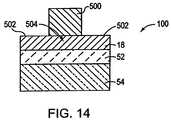
- FIG. 14is a schematic cross-sectional view of the SSOI substrate illustrated in FIG. 6 after additional processing.
- FIGS. 15A-16Dare schematic cross-sectional views of substrates illustrating alternative methods for fabricating an SSOI substrate.
- FIGS. 1A-2Billustrate formation of a suitable strained layer on a wafer for bonding, as further described below.
- an epitaxial wafer 8has a plurality of layers 10 disposed over a substrate 12 .
- Substrate 12may be formed of a semiconductor, such as Si, Ge, or SiGe.
- a relaxed layer 16is disposed over graded buffer layer 14 .
- Si 1-x Ge xmay include Si 0.70 Ge 0.30 and T 2 may be approximately 1.5 ⁇ m.
- Relaxed layer 16may be fully relaxed, as determined by triple axis X-ray diffraction, and may have a threading dislocation density of ⁇ 1 ⁇ 10 6 dislocations/cm 2 , as determined by etch pit density (EPD) analysis.
- EPDetch pit density
- threading dislocation densitymay be measured as either the number of dislocations intersecting a unit area within a unit volume or the line length of dislocation per unit volume. Threading dislocation density therefore, may, be expressed in either units of dislocations/cm 2 or cm/cm 3 .
- Relaxed layer 16may have a surface particle density of, e.g., less than about 0.3 particles/cm 2 .
- relaxed layer 16 produced in accordance with the present inventionmay have a localized light-scattering defect level of less than about 0.3 defects/cm 2 for particle defects having a size (diameter) greater than 0.13 microns, a defect level of about 0.2 defects/cm 2 for particle defects having a size greater than 0.16 microns, a defect level of about 0.1 defects/cm 2 for particle defects having a size greater than 0.2 microns, and a defect level of about 0.03 defects/cm 2 for defects having a size greater than 1 micron.
- Process optimizationmay enable reduction of the localized light-scattering defect levels to about 0.09 defects/cm 2 for particle defects having a size greater than 0.09 microns and to 0.05 defects/cm 2 for particle defects having a size greater than 0.12 microns.
- Substrate 12 , graded layer 14 , and relaxed layer 16may be formed from various materials systems, including various combinations of group II, group III, group IV, group V, and group VI elements.
- each of substrate 12 , graded layer 14 , and relaxed layer 16may include a III-V compound.
- Substrate 12may include gallium arsenide (GaAs)
- graded layer 14 and relaxed layer 16may include indium gallium arsenide (InGaAs) or aluminum gallium arsenide (AlGaAs). These examples are merely illustrative, and many other material systems are suitable.
- a strained semiconductor layer 18is disposed over relaxed layer 16 .
- Strained layer 18may include a semiconductor such as at least one of a group II, a group III, a group IV, a group V, and a group VI element.
- Strained semiconductor layer 18may include, for example, Si, Ge, SiGe, GaAs, indium phosphide (InP), and/or zinc selenide (ZnSe).
- strained semiconductor layer 18may include approximately 100% Ge, and may be compressively strained.
- Strained layer 18has a thickness T 3 of, for example, 50-1000 ⁇ . In an embodiment, T 3 may be approximately 200-500 ⁇ .
- Strained layer 18may be formed by epitaxy, such as by atmospheric-pressure CVD (APCVD), low- (or reduced-) pressure CVD (LPCVD), ultra-high-vacuum CVD (UHVCVD), by molecular beam epitaxy (MBE), or by atomic layer deposition (ALD).
- APCVDatmospheric-pressure CVD
- LPCVDlow- (or reduced-) pressure CVD
- UHVCVDultra-high-vacuum CVD
- MBEmolecular beam epitaxy
- ALDatomic layer deposition
- Strained layer 18 containing Simay be formed by CVD with precursors such as silane, disilane, or trisilane.
- Strained layer 18 containing Gemay be formed by CVD with precursors such as germane or digermane.
- the epitaxial growth systemmay be a single-wafer or multiple-wafer batch reactor. The growth system may also utilize a low-energy plasma to enhance layer growth kinetics.
- Strained layer 18may be formed at a relatively low temperature, e.g., less than 700° C., to facilitate the definition of an abrupt interface 17 between strained layer 18 and relaxed layer 16 .
- This abrupt interface 17may enhance the subsequent separation of strained layer 18 from relaxed layer 16 , as discussed below with reference to FIGS. 4 and 5 .
- Abrupt interface 17is characterized by the transition of Si or Ge content (in this example) proceeding in at least 1 decade (order of magnitude in atomic concentration) per nanometer of depth into the sample. In an embodiment, this abruptness may be better than 2 decades per nanometer.
- strained layer 18may be formed in a dedicated chamber of a deposition tool that is not exposed to Ge source gases, thereby avoiding cross-contamination and improving the quality of the interface between strained layer 18 and relaxed layer 16 .
- strained layer 18may be formed from an isotopically pure silicon precursor(s). Isotopically pure Si has better thermal conductivity than conventional Si. Higher thermal conductivity may help dissipate heat from devices subsequently formed on strained layer 18 , thereby maintaining the enhanced carrier mobilities provided by strained layer 18 .
- strained layer 18After formation, strained layer 18 has an initial misfit dislocation density, of, for example, 0-10 5 cm/cm 2 . In an embodiment, strained layer 18 has an initial misfit dislocation density of approximately 0 cm/cm 2 . Because misfit dislocations are linear defects generally lying within a plane between two crystals within an area, they may be measured in terms of total line length per unit area. Misfit dislocation density, therefore, may be expressed in units of dislocations/cm or cm/cm 2 . In one embodiment, strained layer 18 is tensilely strained, e.g., Si formed over SiGe. In another embodiment, strained layer 18 is compressively strained, e.g., Ge formed over SiGe.
- Strained layer 18may have a surface particle density of, e.g., less than about 0.3 particles/cm 2 .
- surface particle densityincludes not only surface particles but also light-scattering defects, and crystal-originated pits (COPs), and other defects incorporated into strained layer 18 .
- strained layer 18 produced in accordance with the present inventionmay have a localized light-scattering defect level of less than about 0.3 defects/cm 2 for particle defects having a size (diameter) greater than 0.13 microns, a defect level of about 0.2 defects/cm 2 for particle defects having a size greater than 0.16 microns, a defect level of about 0.1 defects/cm 2 for particle defects having a size greater than 0.2 microns, and a defect level of about 0.03 defects/cm 2 for defects having a size greater than 1 micron.
- Process optimizationmay enable reduction of the localized light-scattering defect levels to about 0.09 defects/cm 2 for particle defects having a size greater than 0.09 microns and to 0.05 defects/cm 2 for particle defects having a size greater than 0.12 microns.
- These surface particlesmay be incorporated in strained layer 18 during the formation of strained layer 18 , or they may result from the propagation of surface defects from an underlying layer, such as relaxed layer 16 .
- graded layer 14may be absent from the structure.
- Relaxed layer 16may be formed in various ways, and the invention is not limited to embodiments having graded layer 14 .
- strained layer 18may be formed directly on substrate 12 . In this case, the strain in layer 18 may be induced by lattice mismatch between layer 18 and substrate 12 , induced mechanically, e.g., by the deposition of overlayers, such as Si 3 N 4 , or induced by thermal mismatch between layer 18 and a subsequently grown layer, such as a SiGe layer.
- a uniform semiconductor layer(not shown), having a thickness of approximately 0.5 ⁇ m and comprising the same semiconductor material as substrate 12 , is disposed between graded buffer layer 14 and substrate 12 .
- This uniform semiconductor layermay be grown to improve the material quality of layers subsequently grown on substrate 12 , such as graded buffer layer 14 , by providing a clean, contaminant-free surface for epitaxial growth.
- relaxed layer 16may be planarized prior to growth of strained layer 18 to eliminate the crosshatched surface roughness induced by graded buffer layer 14 . (See, e.g., M. T. Currie, et al., Appl. Phys. Lett., 72 (14) p.
- the planarizationmay be performed by a method such as chemical mechanical polishing (CMP), and may improve the quality of a subsequent bonding process (see below) because it minimizes the wafer surface roughness and increases wafer flatness, thus providing a greater surface area for bonding.
- CMPchemical mechanical polishing
- a relaxed semiconductor regrowth layer 19 including a semiconductor such as SiGemay be grown on relaxed layer 16 , thus improving the quality of subsequent strained layer 18 growth by ensuring a clean surface for the growth of strained layer 18 .
- Growing on this clean surfacemay be preferable to growing strained material, e.g., silicon, on a surface that is possibly contaminated by oxygen and carbon from the planarization process.
- the conditions for epitaxy of the relaxed semiconductor regrowth layer 19 on the planarized relaxed layer 16should be chosen such that surface roughness of the resulting structure, including layers formed over regrowth layer 19 , is minimized to ensure a surface suitable for subsequent high quality bonding.
- High quality bondingmay be defined as the existence of a bond between two wafers that is substantially free of bubbles or voids at the interface. Measures that may help ensure a smooth surface for strained layer 18 growth, thereby facilitating bonding, include substantially matching a lattice of the semiconductor regrowth layer 19 to that of the underlying relaxed layer 16 , by keeping the regrowth thickness below approximately 1 ⁇ m, and/or by keeping the growth temperature below approximately 850° C. for at least a portion of the semiconductor layer 19 growth. It may also be advantageous for relaxed layer 16 to be substantially free of particles or areas with high threading dislocation densities (i.e., threading dislocation pile-ups) which could induce non-planarity in the regrowth and decrease the quality of the subsequent bond.
- threading dislocation densitiesi.e., threading dislocation pile-ups
- hydrogen ionsare implanted into relaxed layer 16 to define a cleave plane 20 .
- This implantationis similar to the SMARTCUT process that has been demonstrated in silicon by, e.g., SOITEC, based in Grenoble, France.
- Implantation parametersmay include implantation of hydrogen (H 2 + ) to a dose of 2.5-5 ⁇ 10 16 ions/cm 2 at an energy of, e.g., 50-100 keV.
- H 2 +may be implanted at an energy of 75 keV and a dose of 4 ⁇ 10 16 ions/cm 2 through strained layer 18 into relaxed layer 16 .
- other implanted speciesmay be used, such as H + or He + , with the dose and energy being adjusted accordingly.
- the implantationmay also be performed prior to the formation of strained layer 18 .
- the subsequent growth of strained layer 18is preferably performed at a temperature low enough to prevent premature cleaving along cleave plane 20 , i.e., prior to the wafer bonding process.
- This cleaving temperatureis a complex function of the implanted species, implanted dose, and implanted material. Typically, premature cleaving may be avoided by maintaining a growth temperature below approximately 500° C.
- a thin layer 21 of another material, such as Si,may be formed over strained layer 18 prior to bonding (see discussion with respect to FIG. 3 ).
- This thin layer 21may be formed to enhance subsequent bonding of strained layer 18 to an insulator, such as an oxide.
- Thin layer 21may have a thickness T 21 of, for example, 0.5-5 nm.
- strained layer 18may be planarized by, e.g., CMP, to improve the quality of the subsequent bond.
- Strained layer 18may have a low surface roughness, e.g., less than 0.5 nm root mean square (RMS).
- RMSroot mean square
- a dielectric layer 22may be formed over strained layer 18 prior to ion implantation into relaxed layer 16 to improve the quality of the subsequent bond.
- Dielectric layer 22may be, e.g., silicon dioxide (SiO 2 ) deposited by, for example, LPCVD or by high density plasma (HDP). An LPCVD deposited SiO 2 layer may be subjected to a densification step at elevated temperature.
- Suitable conditions for this densification stepmay be, for example, a 10 minute anneal at 800° C. in a nitrogen ambient.
- dielectric layer 22may include low-temperature oxide (LTO), which may be subsequently densified at elevated temperature in nitrogen or oxygen ambients.
- LTOlow-temperature oxide
- Suitable conditions for this densification stepcan be a 10 minute anneal at 800° C. in an oxygen ambient.
- Dielectric layer 22may be planarized by, e.g., CMP to improve the quality of the subsequent bond.
- strained layer 18comprises approximately 100% Ge and dielectric layer 22 comprises, for example, germanium dioxide (GeO 2 ); germanium oxynitride (GeON); a high-k insulator having a higher dielectric constant than that of Si such as hafnium oxide (HfO 2 ) or hafnium silicate (HfSiON, HfSiO 4 ); or a multilayer structure including GeO 2 and SiO 2 .
- Gehas an oxidation behavior different from that of Si, and the deposition methods may be altered accordingly.
- epitaxial wafer 8is bonded to a handle wafer 50 .
- Either handle wafer 50 , epitaxial wafer 8 , or bothhave a top dielectric layer (see, e.g., dielectric layer 22 in FIG. 2B ) to facilitate the bonding process and to serve as an insulator layer in the final substrate structure.
- Handle wafer 50may have a dielectric layer 52 disposed over a semiconductor substrate 54 .
- Dielectric layer 52may include, for example, SiO 2 .
- dielectric layer 52includes a material having a melting point (T m ) higher than a T m of pure SiO 2 , i.e., higher than 1700° C.
- handle wafer 50may include a combination of a bulk semiconductor material and a dielectric layer, such as a silicon on insulator substrate.
- Semiconductor substrate 54includes a semiconductor material such as, for example, Si, Ge, or SiGe.
- Handle wafer 50 and epitaxial wafer 8are cleaned by a wet chemical cleaning procedure to facilitate bonding, such as by a hydrophilic surface preparation process to assist the bonding of a semiconductor material, e.g., strained layer 18 , to a dielectric material, e.g., dielectric layer 52 .
- a suitable prebonding surface preparation cleaning procedurecould include a modified megasonic RCA SC1 clean containing ammonium hydroxide, hydrogen peroxide, and water (NH 4 OH:H 2 O 2 :H 2 O) at a ratio of 1:4:20 at 60° C. for 10 minutes, followed by a deionized (DI) water rinse and spin dry.
- DIdeionized
- top surfaces 60 , 62 of handle wafer 50 and epitaxial wafer 8may be subjected to a plasma activation, either before, after, or instead of a wet clean, to increase the bond strength.
- the plasma environmentmay include at least one of the following species: oxygen, ammonia, argon, nitrogen, diborane, and phosphine.
- handle wafer 50 and epitaxial wafer 8are bonded together by bringing top surfaces 60 , 62 in contact with each other at room temperature.
- the bond strengthmay be greater than 1000 mJ/m 2 , achieved at a low temperature, such as less than 600° C.
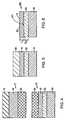
- a splitis induced at cleave plane 20 by annealing handle wafer 50 and epitaxial wafer 8 after they are bonded together.
- This splitmay be induced by an anneal at 300-700° C., e.g., 550° C., inducing hydrogen exfoliation layer transfer (i.e., along cleave plane 20 ) and resulting in the formation of two separate wafers 70 , 72 .
- One of these wafers ( 70 )has a first portion 80 of relaxed layer 16 (see FIG. 1A ) disposed over strained layer 18 .
- Strained layer 18is in contact with dielectric layer 52 on semiconductor substrate 54 .
- the other of these wafers ( 72 )includes substrate 12 , graded layer 14 , and a remaining portion 82 of relaxed layer 16 .
- wafer splittingmay be induced by mechanical force in addition to or instead of annealing.
- wafer 70 with strained layer 18may be annealed further at 600-900° C., e.g., at a temperature greater than 800° C., to strengthen the bond between the strained layer 18 and dielectric layer 52 . In some embodiments, this anneal is limited to an upper temperature of about 900° C. to avoid the destruction of a strained Si/relaxed SiGe heterojunction by diffusion.
- Wafer 72may be planarized, and used as starting substrate 8 for growth of another strained layer 18 .
- wafer 72may be “recycled” and the process illustrated in FIGS. 1A-5 may be repeated.
- An alternative “recyling” methodmay include providing relaxed layer 16 that is several microns thick and repeating the process illustrated in FIGS. 1A-5 , starting with the formation of strained layer 18 . Because the formation of this thick relaxed layer 16 may lead to bowing of substrate 12 , a layer including, e.g., oxide or nitride, may be formed on the backside of substrate 12 to counteract the bowing. Alternatively substrate 12 may be pre-bowed when cut and polished, in anticipation of the bow being removed by the formation of thick relaxed layer 16 .
- relaxed layer portion 80is removed from strained layer 18 .
- removal of relaxed layer portion 80includes oxidizing the relaxed layer portion 80 by wet (steam) oxidation. For example, at temperatures below approximately 800° C., such as temperatures between 600-750° C., wet oxidation will oxidize SiGe much more rapidly then Si, such that the oxidation front will effectively stop when it reaches the strained layer 18 , in embodiments in which strained layer 18 includes Si.
- the difference between wet oxidation rates of SiGe and Simay be even greater at lower temperatures, such as approximately 400° C.-600° C.
- SiGemay be efficiently removed at low temperatures with oxidation stopping when strained layer 18 is reached.
- This wet oxidationresults in the transformation of SiGe to a thermal insulator 90 , e.g., Si x Ge y O z .
- the thermal insulator 90 resulting from this oxidationis removed in a selective wet or dry etch, e.g., wet hydrofluoric acid. In some embodiments, it may be more economical to oxidize and strip several times, instead of just once.
- wet oxidationmay not completely remove the relaxed layer portion 80 .
- a localized rejection of Gemay occur during oxidation, resulting in the presence of a residual Ge-rich SiGe region at the oxidation front, on the order of, for example, several nanometers in lateral extent.
- a surface cleanmay be performed to remove this residual Ge.
- the residual Gemay be removed by a dry oxidation at, e.g., 600° C., after the wet oxidation and strip described above.
- Another wet cleanmay be performed in conjunction with—or instead of—the dry oxidation.
- Examples of possible wet etches for removing residual Geinclude a Piranha etch, i.e., a wet etch that is a mixture of sulfuric acid and hydrogen peroxide (H 2 SO 4 :H 2 O 2 ) at a ratio of, for example, 3:1.
- An HF dipmay be performed after the Piranha etch.
- an RCA SC1 cleanmay be used to remove the residual Ge.
- the process of Piranha or RCA SC1 etching and HF removal of resulting oxidemay be repeated more than once.
- relaxed layer portion including, e.g., SiGeis removed by etching and annealing under a hydrochloric acid (HCl) ambient.
- HClhydrochloric acid
- the surface Ge concentration of the final strained Si surfaceis preferably less than about 1 ⁇ 10 12 atoms/cm 2 when measured by a technique such as total reflection x-ray fluorescence (TXRF) or the combination of vapor phase decomposition (VPD) with a spectroscopy technique such as graphite furnace atomic absorption spectroscopy (GFAAS) or inductively-coupled plasma mass spectroscopy (ICP-MS).
- TXRFtotal reflection x-ray fluorescence
- VPDvapor phase decomposition
- GFAASgraphite furnace atomic absorption spectroscopy
- ICP-MSinductively-coupled plasma mass spectroscopy
- a smoother surfacemay improve the uniformity of subsequent complete removal of a remainder of relaxed layer portion 80 by, e.g., wet chemical etching.
- strained layer 18may be planarized. Planarization of strained layer 18 may be performed by, e.g., CMP; an anneal at a temperature greater than, for example, 800° C., in a hydrogen (H 2 ) or hydrochloric acid (HCl) containing ambient; or cluster ion beam smoothing.
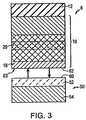
- a SSOI substrate 100has strained layer 18 disposed over an insulator, such as dielectric layer 52 formed on semiconductor substrate 54 .
- Strained layer 18has a thickness T 4 selected from a range of, for example, 50-1000 ⁇ , with a thickness uniformity of better than approximately ⁇ 5% and a surface roughness of less than approximately 20 ⁇ .
- Dielectric layer 52has a thickness T 52 selected from a range of, for example, 500-3000 ⁇ .
- strained layer 18includes approximately 100% Si or 100% Ge having one or more of the following material characteristics: misfit dislocation density of, e.g., 0-10 5 cm/cm 2 ; a threading dislocation density of about 10 1 -10 7 dislocations/cm 2 ; a surface roughness of approximately 0.01-1 nm RMS; and a thickness uniformity across SSOI substrate 100 of better than approximately ⁇ 10% of a mean desired thickness; and a thickness T 4 of less than approximately 200 ⁇ .
- SSOI substrate 100has a thickness uniformity of better than approximately ⁇ 5% of a mean desired thickness.
- dielectric layer 52has a T m greater than that of SiO 2 .
- SSOI substrate 100may be subjected to high temperatures, i.e., up to 1100° C. High temperatures may result in the relaxation of strained layer 18 at an interface between strained layer 18 and dielectric layer 52 .
- the use of dielectric layer with a T m greater than 1700° C.may help keep strained layer 18 from relaxing at the interface between strained layer 18 and dielectric layer 52 when SSOI substrate is subjected to high temperatures.
- the misfit dislocation density of strained layer 18may be lower than its initial dislocation density.
- the initial dislocation densitymay be lowered by, for example, performing an etch of a top surface 92 of strained layer 18 .
- This etchmay be a wet etch, such as a standard microelectronics clean step such as an RCA SC1, i.e., hydrogen peroxide, ammonium hydroxide, and water (H 2 O 2 +NH 4 OH+H 2 O), which at, e.g., 80° C. may remove silicon.
- bonding voidsmay have a density equivalent to the density of surface particles formed on strained layer 18 , e.g., less than about 0.3 voids/cm 2 .
- strained semiconductor layer 18includes Si and is substantially free of Ge; further, any other layer disposed in contact with strained semiconductor layer 18 prior to device processing, e.g., dielectric layer 52 , is also substantially free of Ge.
- relaxed layer portion 80may be removed by a selective wet etch that stops at the strained layer 18 to obtain SSOI substrate 100 (see FIG. 6 ).
- a suitable selective SiGe wet etchmay be a solution containing nitric acid (HNO 3 ) and dilute HF at a ratio of 3:1 or a solution containing H 2 O 2 , HF, and acetic acid (CH 3 COOH) at a ratio of 2:1:3.
- relaxed layer portion 80may be removed by a dry etch that stops at strained layer 18 .
- relaxed layer portion 80may be removed completely or in part by a chemical-mechanical polishing step or by mechanical grinding.
- Strained semiconductor-on-insulator substrate 100may be further processed by CMOS SOI MOSFET fabrication methods.
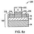
- a transistor 200may be formed on SSOI substrate 100 .
- Forming transistor 200includes forming a gate dielectric layer 210 above strained layer 18 by, for example, growing an SiO 2 layer by thermal oxidation.
- gate dielectric layer 210may include a high-k material with a dielectric constant higher than that of SiO 2 , such as HfO 2 , HfSiON, or HfSiO 4 .
- gate dielectric layer 210may be a stacked structure, e.g., a thin SiO 2 layer capped with a high-k material.
- Gate 212is formed over gate dielectric layer 210 .
- Gate 212may be formed of a conductive material, such as doped semiconductor, e.g., polycrystalline Si or polycrystalline SiGe; a metal, e.g., titanium (Ti), tungsten (W), molybdenum (Mo), tantalum (Ta), nickel (Ni), or iridium (Ir); or metal compounds, e.g., titanium nitride (TiN), titanium silicon nitride (TiSiN), tungsten nitride (WN), tantalum nitride (TaN), tantalum silicide (TaSi), nickel silicide (NiSi), or iridium oxide (IrO 2 ), that provide an appropriate workfunction.
- a conductive materialsuch as doped semiconductor, e.g., polycrystalline Si or polycrystalline SiGe
- a metale.g., titanium (Ti), tungsten (W), mo
- Source region 214 and a drain region 216are formed in a portion 218 of strained semiconductor layer 18 , proximate gate dielectric layer 210 .
- Source and drain regions 214 , 216may be formed by, e.g., ion implantation of either n-type or p-type dopants.
- strained semiconductor layer 18may be compressively strained when, for example, layer 18 includes strained Ge. Compressively strained layers may be prone to undulation when subjected to large temperature changes. The risk of such undulation may be reduced by reducing the thermal budget of a process for fabricating devices, such as transistor 200 . The thermal budget may reduced by, for example, using atomic layer deposition (ALD) to deposit gate dielectric layer 210 . Furthermore, a maximum temperature for forming gate 212 may be limited to, e.g., 600° C. by, for example, the use of materials comprising metal or metal compounds, rather than polysilicon or other gate materials that may require higher formation and/or dopant activation temperatures.
- ALDatomic layer deposition
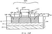
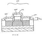
- a transistor 250 formed on SSOI substrate 100may have an elevated source region and an elevated drain region proximate a first and a second sidewall spacer 252 , 254 .
- These elevated regionsmay be formed as follows.
- a semiconductor layer 256 a - 256 cis formed selectively on exposed silicon surfaces, i.e., on top surface 258 of a gate 259 containing silicon, a top surface 260 of a source 262 defined in strained layer 18 , and top surface 264 of a drain 266 defined in strained layer 18 .
- semiconductor layer 256 a - 256 cis an epitaxial layer, such as epitaxial silicon, epitaxial germanium, or epitaxial silicon-germanium.
- No semiconductor layeris formed on non-silicon features, such as sidewall spacers 252 , 254 and dielectric isolation regions 268 , 270 .
- Semiconductor layer 256 a - 256 chas a thickness T 256 of, for example, approximately 100-500 ⁇ .
- Semiconductor layer 256 a - 256 chas a low resistivity of, e.g., 0.001 ohm-cm, that facilitates the formation of low-resistance contacts.
- semiconductor layer 256 a - 256 cis, for example, epitaxial silicon doped with, for example, arsenic to a concentration of 1 ⁇ 10 20 atoms/cm 3 .
- Semiconductor layer 256 a - 256 cmay be doped in situ, during deposition. In alternative embodiments, semiconductor layer 256 a - 256 c may be doped after deposition by ion implantation or by gas-, plasma- or solid-source diffusion.
- the doping of semiconductor layer 256 a - 256 c and the formation of source 262 and drain 266are performed simultaneously. Portions of semiconductor layer 256 a, 256 c disposed over source 262 and drain 266 may have top surfaces substantially free of facets. In an embodiment, portions of source 262 , drain 266 , and/or gate 259 may be etched away to define recess prior to deposition of semiconductor layer 256 a - 256 c, and semiconductor layer 256 a - 256 c may then be deposited in the recesses thus formed.
- Metal layer 272is formed over transistor 250 .
- Metal layer 272is formed by, for example, sputter deposition.
- Metal layer 272has a thickness T 272 of, e.g., 50-200 ⁇ and includes a metal such as cobalt, titanium, tungsten, nickel, or platinum.
- the metalis selected to react with semiconductor layer 256 a - 256 c to form a low-resistance metal-semiconductor alloy when exposed to heat, as described below.
- the metalis also selected such that the metal-semiconductor alloy remains stable at temperatures typically required to complete transistor 250 fabrication, e.g., 400-700° C.
- a first rapid thermal annealis performed, e.g., at 550° C. for 60 seconds.
- This heating stepinitiates a reaction between metal layer 272 and semiconductor layers 256 a - 256 c, forming a high resistivity phase of a metal-semiconductor alloy, e.g., cobalt silicide. (CoSi).
- a wet etchsuch as sulfuric acid and hydrogen peroxide.
- the wet etchmay be ammonium hydroxide, peroxide, and water.
- This wet etchremoves portions of metal layer 272 disposed over dielectric material, such as over first and second sidewall spacers 252 , 254 and isolation regions 268 , 270 . Portions 274 of metal layer 272 disposed over semiconductor layer 256 a - 256 c that have reacted to form the metal-semiconductor alloy remain in place after the anneal and wet etch.
- SSOI substrate 100including transistor 250 , is subjected to a second heat treatment.
- SSOI substrate 100undergoes a rapid thermal anneal at 800° C. for 60 seconds in a nitrogen ambient. This heating step initiates a reaction in the metal-semiconductor alloy layer which substantially lowers its resistivity, to form a substantially homogeneous contact layer 276 a - 276 c.
- Contact layer 276 a - 276 cincludes a metal-semiconductor alloy, e.g., a metal silicide such as a low resistivity phase of cobalt silicide (CoSi 2 ).
- Contact layer 276 a - 276 chas a thickness T 276 of, for example, 400 ⁇ .
- Contact layer 276 a - 276 chas a low sheet resistance, e.g., less than about 10 ⁇ / ⁇ , and enables a good quality contact to be made to source 262 and drain 266 , as well as to gate 259 .
- contact layer 276 a - 276 cmay consume substantially all of semiconductor layer 256 a - 256 c.
- a bottommost boundary 278 a of contact layer 276 atherefore, shares an interface 280 a with strained layer 18 in source 262
- a bottommost boundary 278 c of contact layer 276 ctherefore, shares an interface 280 c with strained layer 18 in drain 266 .
- a bottommost boundary 278 b of contact layer 276 bshares an interface 280 b with gate 259 .
- contact layer portions 276 a, 276 c, disposed over source 262 and drain 266may extend into strained layer 18 .
- Interfaces 280 a, 280 c between contact layer 276 a, 276 c and strained layer 18are then disposed within source 262 and drain 266 , respectively, above bottommost boundaries 282 a, 282 c of strained layer 18 .
- Interfaces 280 a, 280 chave a low contact resistivity, e.g., less than approximately 5 ⁇ 10 ⁇ 7 ⁇ -cm 2 .
- contact layer 276 a - 276 cmay not consume all of semiconductor layer 256 a - 256 c (see FIG. 8D ).
- a bottommost boundary 278 a of contact layer 276 atherefore, shares an interface with semiconductor layer 256 a over source 262
- a bottommost boundary 278 c of contact layer 276 ctherefore, shares an interface with semiconductor layer 256 c over drain 266 .
- strained layer 18includes a strained material, carrier mobilities in strained layer 18 are enhanced, facilitating lower sheet resistances. This strain also results in a reduced energy bandgap, thereby lowering the contact resistivity between the metal-semiconductor alloy and the strained layer.
- an SSOI structuremay include, instead of a single strained layer, a plurality of semiconductor layers disposed on an insulator layer.
- epitaxial wafer 300includes strained layer 18 , relaxed layer 16 , graded layer 14 , and substrate 12 .
- a semiconductor layer 310is disposed over strained layer 18 .
- Strained layer 18may be tensilely strained and semiconductor layer 310 may be compressively strained.
- strained layer 18may be compressively strained and semiconductor layer 310 may be tensilely strained. Strain may be induced by lattice mismatch with respect to an adjacent layer, as described above, or mechanically.
- strainmay be induced by the deposition of overlayers, such as Si 3 N 4 .
- semiconductor layer 310is relaxed.
- Semiconductor layer 310includes a semiconductor material, such as at least one of a group II, a group III, a group IV, a group V, and a group VI element.
- Epitaxial wafer 300is processed in a manner analogous to the processing of epitaxial wafer 8 , as described with reference to FIGS. 1-7 .
- processing of epitaxial wafer 300results in the formation of SSOI substrate 350 , having strained layer 18 disposed over semiconductor layer 310 .
- Semiconductor layer 310is bonded to dielectric layer 52 , disposed over substrate 54 .
- strained layer 18may be tensilely strained and semiconductor layer 310 may be compressively strained.
- strained layer 18may be compressively strained and semiconductor layer 310 may be tensilely strained.
- semiconductor layer 310may be relaxed.
- a thin strained layer 84may be grown between strained layer 18 and relaxed layer 16 to act as an etch stop during etching, such as wet etching.
- thin strained layer 84may include Si 1-x Ge x , with a higher Ge content (x) than the Ge content (y) of relaxed layer 16 , and hence be compressively strained.
- the composition of the relaxed layer 16is 20% Ge (Si 0.80 Ge 0.20 )
- thin strained layer 84may contain 40% Ge (Si 0.60 Ge 0.40 ) to provide a more robust etch stop.
- a second strained layersuch as thin strained layer 84 with higher Ge content than relaxed layer 16 , may act as a preferential cleave plane in the hydrogen exfoliation/cleaving procedure described above.
- thin strained layer 84may contain Si 1-x Ge x with lower Ge content than relaxed layer 16 .
- thin strained layer 84may act as a diffusion barrier during the wet oxidation process. For example, if the composition of relaxed layer 16 is 20% Ge (Si 0.80 Ge 0.20 ), thin strained layer 84 may contain 10% Ge (Si 0.90 Ge 0.10 ) to provide a barrier to Ge diffusion from the higher Ge content relaxed layer 16 during the oxidation process.
- thin strained layer 84may be replaced with a thin graded Si 1-z Ge z layer in which the Ge composition (z) of the graded layer is decreased from relaxed layer 16 to the strained layer 18 .
- a small amount, e.g., approximately 20-100 ⁇ , of strained layer 18may be removed at an interface 105 between strained layer 18 and relaxed layer portion 80 . This may be achieved by overetching after relaxed layer portion 80 is removed. Alternatively, this removal of strained layer 18 may be performed by a standard microelectronics clean step such as an RCA SC1, i.e., hydrogen peroxide, ammonium hydroxide, and water (H 2 O 2 +NH 4 OH+H 2 O), which at, e.g., 80° C. may remove silicon.
- RCA SC1i.e., hydrogen peroxide, ammonium hydroxide, and water (H 2 O 2 +NH 4 OH+H 2 O)
- This silicon removalmay remove any misfit dislocations that formed at the original strained layer 18 /relaxed layer 80 interface 105 if strained layer 18 was grown above the critical thickness.
- the critical thicknessmay be defined as the thickness of strained layer 18 beyond which it becomes energetically favorable for the strain in the layer to partially relax via the introduction of misfit dislocations at interface 105 between strained layer 18 and relaxed layer 16 .
- the method illustrated in FIGS. 1-7provides a technique for obtaining strained layers above a critical thickness without misfit dislocations that may compromise the performance of deeply scaled MOSFET devices.
- handle wafer 50may have a structure other than a dielectric layer 52 disposed over a semiconductor substrate 54 .
- a bulk relaxed substrate 400may comprise a bulk material 410 such as a semiconductor material, e.g., bulk silicon.
- bulk material 410may be a bulk dielectric material, such as Al 2 O 3 (e.g., alumina or sapphire) or SiO 2 (e.g., quartz).
- Epitaxial wafer 8may then be bonded to handle wafer 400 (as described above with reference to FIGS. 1-6 ), with strained layer 18 being bonded to the bulk material 410 comprising handle wafer 400 .
- a hydrophobic cleanmay be performed, such as an HF dip after an RCA SC1 clean.
- a strained-semiconductor-on-semiconductor (SSOS) substrate 420is formed, having strained layer 18 disposed in contact with relaxed substrate 400 .
- the strain of strained layer 18is not induced by underlying relaxed substrate 400 , and is independent of any lattice mismatch between strained layer 18 and relaxed substrate 400 .
- strained layer 18 and relaxed substrate 400include the same semiconductor material, e.g., silicon.
- Relaxed substrate 400may have a lattice constant equal to a lattice constant of strained layer 18 in the absence of strain.
- Strained layer 18may have a strain greater than approximately 1 ⁇ 10 ⁇ 3 .
- Strained layer 18may have been formed by epitaxy, and may have a thickness T 5 of between approximately 20 ⁇ -1000 ⁇ , with a thickness uniformity of better than approximately ⁇ 10%. In an embodiment, strained layer 18 may have a thickness uniformity of better than approximately ⁇ 5%. Surface 92 of strained layer 18 may have a surface roughness of less than 20 ⁇ .
- the SSOI structure 100including semiconductor substrate 54 and dielectric layer 52 , it may be favorable to selectively relax the strain in at least a portion of strained layer 18 .
- Ion implantation parametersmay be, for example, an implant of Si ions at a dose of 1 ⁇ 10 15 -1 ⁇ 10 17 ions/cm 2 , at an energy of 5-75 keV.
- a relaxed portion 502 of strained layer 18is relaxed, while a strained portion 504 of strained layer 18 remains strained.
- SSOI structure 100may be formed by the use of a porous semiconductor substrate.
- substrate 12may be formed of a semiconductor, such as Si, Ge, or SiGe.
- a plurality of pores 1514i.e., microvoids, are formed to define a porous layer 1516 in a portion of substrate 12 .
- Pores 1514may have a median diameter of 5-10 nm and a pitch of 10-50 nm.
- Porous layer 1516may have a porosity of 10-50% and may extend a depth of d 15 into substrate 12 of approximately 1-5 ⁇ m.
- pores 1514may be formed by, for example, submerging substrate 12 into a vessel 1517 containing an electrolyte 1518 , such as hydrofluoric acid (HF), possibly mixed with ethanol, with a cathode 1520 and an anode 1522 disposed in the electrolyte 1518 .
- a back surface chucking holder 1519 a with a vacuum pad 1519 bmay hold substrate 12 while it is submerged in vessel 1517 .
- a currentmay be generated between cathode 1520 and anode 1522 , through substrate 12 , resulting in the electrochemical etching of substrate 12 , thereby forming pores 1514 at a top surface 1524 of substrate 12 .
- substrate 12may be planarized, e.g., by CMP.
- a plurality of layers 10may be formed over porous top surface 1524 of substrate 12 , as described with reference to FIG. 1A .
- Layers 10may include, for example, graded buffer layer 14 , relaxed layer 16 , and strained layer 18 .
- Pores 1514define cleave plane 20 in porous layer 1516 of substrate 12 .
- substrate 12 with layers 10is bonded to handle wafer 50 , including semiconductor substrate 54 and dielectric layer 52 , as described with reference to FIG. 3 .
- a dielectric layermay be formed on a top surface of layers 10 to facilitate the bonding process and to serve as an insulator layer in the final substrate structure.
- a splitis induced at cleave plane 20 by, for example, cleaving porous layer 1516 by a water or an airjet.
- the splitresults in the formation of two separate wafers 1570 , 1572 .
- One of these wafers ( 1572 )has graded layer 14 and relaxed layer 16 (see FIG. 15C ) disposed over strained layer 18 , with a first portion 1580 of substrate 12 disposed over graded layer 14 .
- First portion 1580 of substrate 12may be just trace amounts of material surrounding pores 1514 .
- Strained layer 18is in contact with dielectric layer 52 on semiconductor substrate 54 .
- the other of these wafers ( 1570 )includes a second portion 1582 of substrate 12 , including the bulk of substrate 12 with perhaps trace amounts of material surrounding pores 1514 .
- first portion 1580 of substrate 12is removed from graded layer 14 by a wet chemical cleaning process utilizing, for example a mixture of hydrogen peroxide (H 2 O 2 ) and HF.
- Graded layer 14 and relaxed layer 16are removed in any one of the methods described for the removal of relaxed layer portion 80 with reference to FIGS. 4 and 5 . Removal of graded and relaxed layers 14 , 16 results in the formation of SSOI substrate 100 .
- SSOI substrate 100may also be formed by the use of porous intermediate layers.
- plurality of layers 10may be formed over substrate 12 , layers 10 including graded layer 14 , relaxed layer 16 , and strained layer 18 (see FIG. 1A ).
- a plurality of pores 1614may be formed in a top portion of relaxed layer 16 , thereby defining a porous layer 1616 in a top portion 1617 of relaxed layer 16 .
- Pores 1614may be formed by the methods described above with reference to the formation of pores 1514 in FIG. 15B .
- Porous layer 1616may have a thickness T 16 of, e.g., 1-5 ⁇ m.
- Strained layer 18may then be formed directly over porous layer 1616 .
- Pores 1614define cleave plane 20 in porous layer 1616 .
- Si 1-x Ge xmay include Si 0.70 Ge 0.30 and T 17 may be approximately 50 nm.
- Second relaxed layer 1620may be fully relaxed, as determined by triple axis X-ray diffraction, and may have a threading dislocation density of ⁇ 1 ⁇ 10 6 /cm 2 , as determined by etch pit density (EPD) analysis.
- Strained layer 18may be formed over second relaxed layer 1620 .
- Pores 1614define cleave plane 20 in porous layer 1616 .
- substrate 12 with layers 10is bonded to handle wafer 50 , including semiconductor substrate 54 and dielectric layer 52 , as described with reference to FIG. 3 .
- a splitis induced at cleave plane 20 by, for example, cleaving porous layer 1616 by a water or an air jet.
- the splitresults in the formation of two separate wafers 1670 , 1672 .
- One of these wafers ( 1670 )has top portion 1617 of relaxed layer 16 (see FIG. 16A ) disposed over strained layer 18 .
- Strained layer 18is in contact with dielectric layer 52 on semiconductor substrate 54 .
- the other of these wafers ( 1672 )includes the substrate 12 , graded layer 14 , and a bottom portion 1674 of relaxed layer 16 .
- top portion 1617 of relaxed layer 16is removed in any one of the methods described for the removal of relaxed layer portion 80 with reference to FIGS. 4 and 5 . Removal of top portion 1617 of relaxed layer 16 results in the formation of SSOI substrate 100 .
- strained silicon layer 18having a thickness of 54 nanometers (nm) along with ⁇ 350 nm of Si 0.70 Ge 0.30 have been transferred by hydrogen exfoliation to Si handle wafer 50 having dielectric layer 52 formed from thermal SiO 2 with a thickness of approximately 100 nm.
- the implant conditionswere a dose of 4 ⁇ 10 16 ions/cm 3 of H 2 + at 75 keV.
- the anneal procedurewas 1 hour at 550° C. to split the SiGe layer, followed by a 1 hour, 800° C. strengthening anneal.
- strained Si layer 18The integrity of strained Si layer 18 and good bonding to dielectric layer 52 after layer transfer and anneal were confirmed with cross-sectional transmission electron microscopy (XTEM).
- XTEMcross-sectional transmission electron microscopy
- An SSOI structure 100was characterized by XTEM and analyzed via Raman spectroscopy to determine the strain level of the transferred strained Si layer 18 .
- An XTEM image of the transferred intermediate SiGe/strained Si/SiO 2 structureshowed transfer of the 54 nm strained Si layer 18 and ⁇ 350 nm of the Si 0.70 Ge 0.30 relaxed layer 16 .
- Strained Si layer 18had a good integrity and bonded well to SiO 2 54 layer after the annealing process.
- the final structureincludes strained Si layer 18 having a thickness of 49 nm on dielectric layer 52 including SiO 2 and having a thickness of 100 nm.
- Raman spectroscopy dataenabled a comparison of the bonded and cleaved structure before and after SiGe layer 16 removal. Based on peak positions the compostion of the relaxed SiGe layer and strain in the Si layer may be calculated. See, for example, J. C. Tsang, et al., J. Appl. Phys. 75 (12) p. 8098 (1994), incorporated herein by reference.
- the fabricated SSOI structure 100had a clear strained Si peak visible at ⁇ 511/cm. Thus, the SSOI structure 100 maintained greater than 1% tensile strain in the absence of the relaxed SiGe layer 16 .
- the absence of Ge-Ge, Si-Ge, and Si-Si relaxed SiGe Raman peaks in the SSOI structureconfirmed the complete removal of SiGe layer 16 .
- the thermal stability of the strained Si layerwas evaluated after a 3 minute 1000° C. rapid thermal anneal (RTA) to simulate an aggregate thermal budget of a CMOS process.
- RTArapid thermal anneal
- a Raman spectroscopy comparisionwas made of SSOI structure 100 as processed and after the RTA step.
- a scan of the as-bonded and cleaved sample prior to SiGe layer removalwas used for comparision.
- the strained Si peakwas visible and the peak position did not shift.
- the strain in SSOI structure 100was stable and was not diminished by thermal processing.
- bubbles or flaking of the strained Si surface 18were not observed by Nomarski optical microscopy after the RTA, indicating good mechanical stability of SSOI structure 100 .
Landscapes
- Engineering & Computer Science (AREA)
- Microelectronics & Electronic Packaging (AREA)
- Condensed Matter Physics & Semiconductors (AREA)
- General Physics & Mathematics (AREA)
- Manufacturing & Machinery (AREA)
- Computer Hardware Design (AREA)
- Physics & Mathematics (AREA)
- Power Engineering (AREA)
- Insulated Gate Type Field-Effect Transistor (AREA)
- Thin Film Transistor (AREA)
- Recrystallisation Techniques (AREA)
- Chemical & Material Sciences (AREA)
- Crystallography & Structural Chemistry (AREA)
- Element Separation (AREA)
Abstract
Description
- This application claims the benefit of U.S.
Provisional Application 60/386,968 filed Jun. 7, 2002, U.S.Provisional Application 60/404,058 filed Aug. 15, 2002, and U.S.Provisional Application 60/416,000 filed Oct. 4, 2002; the entire disclosures of these three provisional applications are hereby incorporated by reference. - This invention relates to devices and structures comprising strained semiconductor layers and insulator layers.
- Strained silicon-on-insulator structures for semiconductor devices combine the benefits of two advanced approaches to performance enhancement: silicon-on-insulator (SOI) technology and strained silicon (Si) technology. The strained silicon-on-insulator configuration offers various advantages associated with the insulating substrate, such as reduced parasitic capacitances and improved isolation. Strained Si provides improved carrier mobilities. Devices such as strained Si metal-oxide-semiconductor field-effect transistors (MOSFETs) combine enhanced carrier mobilities with the advantages of insulating substrates.
- Strained-silicon-on-insulator substrates are typically fabricated as follows. First, a relaxed silicon-germanium (SiGe) layer is formed on an insulator by one of several techniques such as separation by implantation of oxygen (SIMOX), wafer bonding and etch back; wafer bonding and hydrogen exfoliation layer transfer; or recrystallization of amorphous material. Then, a strained Si layer is epitaxially grown to form a strained-silicon-on-insulator structure, with strained Si disposed over SiGe. The relaxed-SiGe-on-insulator layer serves as the template for inducing strain in the Si layer. This induced strain is typically greater than 10−3.
- This structure has limitations. It is not conducive to the production of fully-depleted strained-semiconductor-on-insulator devices in which the layer over the insulating material must be thin enough [<300 angstroms (Å)] to allow for full depletion of the layer during device operation. Fully depleted transistors may be the favored version of SOI for MOSFET technologies beyond the 90 nm technology node. The relaxed SiGe layer adds to the total thickness of this layer and thus makes it difficult to achieve the thicknesses required for fully depleted silicon-on-insulator device fabrication. The relaxed SiGe layer is not required if a strained Si layer can be produced directly on the insulating material. Thus, there is a need for a method to produce strained silicon—or other semiconductor—layers directly on insulating substrates.
- The present invention includes a strained-semiconductor-on-insulator (SSOI) substrate structure and methods for fabricating the substrate structure. MOSFETs fabricated on this substrate will have the benefits of SOI MOSFETs as well as the benefits of strained Si mobility enhancement. By eliminating the SiGe relaxed layer traditionally found beneath the strained Si layer, the use of SSOI technology is simplified. For example, issues such as the diffusion of Ge into the strained Si layer during high temperature processes are avoided.
- This approach enables the fabrication of well-controlled, epitaxially-defined, thin strained semiconductor layers directly on an insulator layer. Tensile strain levels of ˜10−3or greater are possible in these structures, and are not diminished after thermal anneal cycles. In some embodiments, the strain-inducing relaxed layer is not present in the final structure, eliminating some of the key problems inherent to current strained Si-on-insulator solutions. This fabrication process is suitable for the production of enhanced-mobility substrates applicable to partially or fully depleted SSOI technology.
- In an aspect, the invention features a structure including a substrate having a dielectric layer disposed thereon; and a first strained semiconductor layer disposed in contact with the dielectric layer, the semiconductor layer including approximately 100% germanium.
- One or more of the following features may be included. The strained semiconductor layer may be compressively strained. The strained semiconductor layer may include a thin layer and the thin layer is disposed in contact with the dielectric layer. The thin layer may include silicon.
- In another aspect, the invention features a substrate having a dielectric layer disposed thereon, a strained semiconductor layer disposed in contact with the dielectric layer, and a transistor. The transistor includes a source region and a drain region disposed in a portion of the strained semiconductor layer, and a gate disposed above the strained semiconductor layer and between the source and drain regions, the gate including a material selected from the group consisting of a doped semiconductor, a metal, and a metallic compound.
- One or more of the following features may be included. The doped semiconductor may include polycrystalline silicon and/or polycrystalline silicon-germanium. The metal may include titanium, tungsten, molybdenum, tantalum, nickel, and/or iridium. The metal compound may include titanium nitride, titanium silicon nitride, tungsten nitride, tantalum nitride, tantalum silicide, nickel silicide, and/or iridium oxide. A contact layer may be disposed over at least a portion of the strained semiconductor layer, with a bottommost boundary of the contact layer being disposed above a bottommost boundary of the strained semiconductor layer. The contact layer may share an interface with the semiconductor layer.
- In another aspect, the invention features a structure including a substrate having a dielectric layer disposed thereon, the dielectric layer having a melting point greater than about 1700° C., and a strained semiconductor layer disposed in contact with the dielectric layer.
- The following features may be included. The dielectric layer may include aluminum oxide, magnesium oxide, and/or silicon nitride.
- In another aspect, the invention features a structure including a substrate having a dielectric layer disposed thereon; and a strained semiconductor layer disposed in contact with the dielectric layer. The strained semiconductor layer includes approximately 100% silicon and has a misfit dislocation density of less than about 105cm/cm2. In another aspect, the invention features a structure including a substrate having a dielectric layer disposed thereon, and a strained semiconductor layer disposed in contact with the dielectric layer. The strained semiconductor layer includes approximately 100% silicon and has a threading dislocation density selected from the range of about 10 dislocations/cm2to about 107dislocations/cm2.
- In another aspect, the invention features a structure including a substrate having a dielectric layer disposed thereon and a strained semiconductor layer disposed in contact with the dielectric layer. The semiconductor layer includes approximately 100% silicon and has a surface roughness selected from the range of approximately 0.01 nm to approximately 1 nm.
- In another aspect, the invention features a substrate having a dielectric layer disposed thereon, and a strained semiconductor layer disposed in contact with the dielectric layer. The strained semiconductor layer includes approximately 100% silicon and has a thickness uniformity across the substrate of better than approximately ±10%.
- In another aspect, the invention features a structure including a substrate having a dielectric layer disposed thereon, and a strained semiconductor layer disposed in contact with the dielectric layer. The strained semiconductor layer includes approximately 100% silicon and has a thickness of less than approximately 200 Å.
- In another aspect, the invention features a structure including a substrate having a dielectric layer disposed thereon, and a strained semiconductor layer disposed in contact with the dielectric layer. The semiconductor layer includes approximately 100% silicon and has a surface germanium concentration of less than approximately 1×10¹²atoms/cm2.
- In another aspect, the invention features a structure including a substrate having a dielectric layer disposed thereon, and a strained semiconductor layer disposed in contact with the dielectric layer. An interface between the strained semiconductor layer and the dielectric layer has a density of bonding voids of less than 0.3 voids/cm2.
- In another aspect, the invention features a method for forming a structure, the method including providing a first substrate comprising a porous layer defining a cleave plane and having a first strained semiconductor layer formed thereon. The first strained semiconductor layer is bonded to an insulator layer disposed on a second substrate, and removing the first substrate from the first strained semiconductor layer by cleaving at the cleave plane, the strained semiconductor layer remaining bonded to the insulator layer.
- In another aspect, the invention features a method for forming a structure, the method including forming a first relaxed layer over a first substrate, the first relaxed layer including a porous layer defining a cleave plane. A strained semiconductor layer is formed over the first relaxed layer. The first strained semiconductor layer is bonded to an insulator layer disposed on a second substrate. The first substrate is removed from the strained semiconductor layer by cleaving at the cleave plane, the strained semiconductor layer remaining bonded to the insulator layer
- One or more of the following features may be included. The porous layer may be disposed at a top portion of the first relaxed layer. A second relaxed layer may be formed over the first relaxed layer, with the strained semiconductor layer being formed over the second relaxed layer. The first relaxed layer may be planarized, e.g., by chemical-mechanical polishing, prior to forming the second relaxed layer. At least a portion of the porous layer may remain disposed on the first strained semiconductor layer after cleaving. The portion of the porous layer may be removed from the strained semiconductor layer after cleaving. The portion of the porous layer may be removed by cleaning with a wet chemical solution that may include, e.g., hydrogen peroxide and/or hydrofluoric acid. Removing the portion of the porous layer may include oxidation.
FIGS. 1A-6 are schematic cross-sectional views of substrates illustrating a method for fabricating an SSOI substrate;FIG. 7 is a schematic cross-sectional view illustrating an alternative method for fabricating the SSOI substrate illustrated inFIG. 6 ;FIG. 8 is a schematic cross-sectional view of a transistor formed on the SSOI substrate illustrated inFIG. 6 ;FIGS. 9-10 are schematic cross-sectional views of substrate(s) illustrating a method for fabricating an alternative SSOI substrate;FIG. 11 is a schematic cross-sectional view of a substrate having several layers formed thereon;FIGS. 12-13 are schematic cross-sectional views of substrates illustrating a method for fabricating an alternative strained semiconductor substrate;FIG. 14 is a schematic cross-sectional view of the SSOI substrate illustrated inFIG. 6 after additional processing; andFIGS. 15A-16D are schematic cross-sectional views of substrates illustrating alternative methods for fabricating an SSOI substrate.- Like-referenced features represent common features in corresponding drawings.
- An SSOI structure may be formed by wafer bonding followed by cleaving.
FIGS. 1A-2B illustrate formation of a suitable strained layer on a wafer for bonding, as further described below. - Referring to
FIG. 1A , anepitaxial wafer 8 has a plurality oflayers 10 disposed over asubstrate 12.Substrate 12 may be formed of a semiconductor, such as Si, Ge, or SiGe. The plurality oflayers 10 includes a gradedbuffer layer 14, which may be formed of Si1-yGey, with a maximum Ge content of, e.g., 10-80% (i.e., y=0.1-0.8) and a thickness T1of, for example, 1-8 micrometers (μm). - A
relaxed layer 16 is disposed over gradedbuffer layer 14.Relaxed layer 16 may be formed of uniform Si1-xGexhaving a Ge content of, for example, 10-80% (i.e., x=0.1-0.8), and a thickness T2of, for example, 0.2-2 μm. In some embodiments, Si1-xGexmay include Si0.70Ge0.30and T2may be approximately 1.5 μm.Relaxed layer 16 may be fully relaxed, as determined by triple axis X-ray diffraction, and may have a threading dislocation density of <1×10⁶dislocations/cm2, as determined by etch pit density (EPD) analysis. Because threading dislocations are linear defects disposed within a volume of crystalline material, threading dislocation density may be measured as either the number of dislocations intersecting a unit area within a unit volume or the line length of dislocation per unit volume. Threading dislocation density therefore, may, be expressed in either units of dislocations/cm2or cm/cm3.Relaxed layer 16 may have a surface particle density of, e.g., less than about 0.3 particles/cm2. Further,relaxed layer 16 produced in accordance with the present invention may have a localized light-scattering defect level of less than about 0.3 defects/cm2for particle defects having a size (diameter) greater than 0.13 microns, a defect level of about 0.2 defects/cm2for particle defects having a size greater than 0.16 microns, a defect level of about 0.1 defects/cm2for particle defects having a size greater than 0.2 microns, and a defect level of about 0.03 defects/cm2for defects having a size greater than 1 micron. Process optimization may enable reduction of the localized light-scattering defect levels to about 0.09 defects/cm2for particle defects having a size greater than 0.09 microns and to 0.05 defects/cm2for particle defects having a size greater than 0.12 microns. Substrate 12, gradedlayer 14, andrelaxed layer 16 may be formed from various materials systems, including various combinations of group II, group III, group IV, group V, and group VI elements. For example, each ofsubstrate 12, gradedlayer 14, andrelaxed layer 16 may include a III-V compound.Substrate 12 may include gallium arsenide (GaAs), gradedlayer 14 andrelaxed layer 16 may include indium gallium arsenide (InGaAs) or aluminum gallium arsenide (AlGaAs). These examples are merely illustrative, and many other material systems are suitable.- A
strained semiconductor layer 18 is disposed overrelaxed layer 16.Strained layer 18 may include a semiconductor such as at least one of a group II, a group III, a group IV, a group V, and a group VI element.Strained semiconductor layer 18 may include, for example, Si, Ge, SiGe, GaAs, indium phosphide (InP), and/or zinc selenide (ZnSe). In some embodiments,strained semiconductor layer 18 may include approximately 100% Ge, and may be compressively strained.Strained semiconductor layer 18 comprising 100% Ge may be formed over, e.g.,relaxed layer 16 containing uniform Si1-xGexhaving a Ge content of, for example, 50-80% (i.e., x=0.5-0.8), preferably 70% (x=0.7).Strained layer 18 has a thickness T3of, for example, 50-1000 Å. In an embodiment, T3may be approximately 200-500 Å. Strained layer 18 may be formed by epitaxy, such as by atmospheric-pressure CVD (APCVD), low- (or reduced-) pressure CVD (LPCVD), ultra-high-vacuum CVD (UHVCVD), by molecular beam epitaxy (MBE), or by atomic layer deposition (ALD).Strained layer 18 containing Si may be formed by CVD with precursors such as silane, disilane, or trisilane.Strained layer 18 containing Ge may be formed by CVD with precursors such as germane or digermane. The epitaxial growth system may be a single-wafer or multiple-wafer batch reactor. The growth system may also utilize a low-energy plasma to enhance layer growth kinetics.Strained layer 18 may be formed at a relatively low temperature, e.g., less than 700° C., to facilitate the definition of anabrupt interface 17 betweenstrained layer 18 andrelaxed layer 16. Thisabrupt interface 17 may enhance the subsequent separation ofstrained layer 18 fromrelaxed layer 16, as discussed below with reference toFIGS. 4 and 5 .Abrupt interface 17 is characterized by the transition of Si or Ge content (in this example) proceeding in at least 1 decade (order of magnitude in atomic concentration) per nanometer of depth into the sample. In an embodiment, this abruptness may be better than 2 decades per nanometer.- In an embodiment in which strained
layer 18 contains substantially 100% Si,strained layer 18 may be formed in a dedicated chamber of a deposition tool that is not exposed to Ge source gases, thereby avoiding cross-contamination and improving the quality of the interface betweenstrained layer 18 andrelaxed layer 16. Furthermore,strained layer 18 may be formed from an isotopically pure silicon precursor(s). Isotopically pure Si has better thermal conductivity than conventional Si. Higher thermal conductivity may help dissipate heat from devices subsequently formed onstrained layer 18, thereby maintaining the enhanced carrier mobilities provided bystrained layer 18. - After formation,
strained layer 18 has an initial misfit dislocation density, of, for example, 0-105cm/cm2. In an embodiment,strained layer 18 has an initial misfit dislocation density of approximately 0 cm/cm2. Because misfit dislocations are linear defects generally lying within a plane between two crystals within an area, they may be measured in terms of total line length per unit area. Misfit dislocation density, therefore, may be expressed in units of dislocations/cm or cm/cm2. In one embodiment,strained layer 18 is tensilely strained, e.g., Si formed over SiGe. In another embodiment,strained layer 18 is compressively strained, e.g., Ge formed over SiGe. Strained layer 18 may have a surface particle density of, e.g., less than about 0.3 particles/cm2. As used herein, “surface particle density” includes not only surface particles but also light-scattering defects, and crystal-originated pits (COPs), and other defects incorporated intostrained layer 18. Further,strained layer 18 produced in accordance with the present invention may have a localized light-scattering defect level of less than about 0.3 defects/cm2for particle defects having a size (diameter) greater than 0.13 microns, a defect level of about 0.2 defects/cm2for particle defects having a size greater than 0.16 microns, a defect level of about 0.1 defects/cm2for particle defects having a size greater than 0.2 microns, and a defect level of about 0.03 defects/cm2for defects having a size greater than 1 micron. Process optimization may enable reduction of the localized light-scattering defect levels to about 0.09 defects/cm2for particle defects having a size greater than 0.09 microns and to 0.05 defects/cm2for particle defects having a size greater than 0.12 microns. These surface particles may be incorporated instrained layer 18 during the formation ofstrained layer 18, or they may result from the propagation of surface defects from an underlying layer, such asrelaxed layer 16.- In alternative embodiments, graded
layer 14 may be absent from the structure.Relaxed layer 16 may be formed in various ways, and the invention is not limited to embodiments having gradedlayer 14. In other embodiments,strained layer 18 may be formed directly onsubstrate 12. In this case, the strain inlayer 18 may be induced by lattice mismatch betweenlayer 18 andsubstrate 12, induced mechanically, e.g., by the deposition of overlayers, such as Si3N4, or induced by thermal mismatch betweenlayer 18 and a subsequently grown layer, such as a SiGe layer. In some embodiments, a uniform semiconductor layer (not shown), having a thickness of approximately 0.5 μm and comprising the same semiconductor material assubstrate 12, is disposed between gradedbuffer layer 14 andsubstrate 12. This uniform semiconductor layer may be grown to improve the material quality of layers subsequently grown onsubstrate 12, such as gradedbuffer layer 14, by providing a clean, contaminant-free surface for epitaxial growth. In certain embodiments,relaxed layer 16 may be planarized prior to growth ofstrained layer 18 to eliminate the crosshatched surface roughness induced by gradedbuffer layer 14. (See, e.g., M. T. Currie, et al.,Appl. Phys. Lett.,72 (14) p. 1718 (1998), incorporated herein by reference.) The planarization may be performed by a method such as chemical mechanical polishing (CMP), and may improve the quality of a subsequent bonding process (see below) because it minimizes the wafer surface roughness and increases wafer flatness, thus providing a greater surface area for bonding. - Referring to
FIG. 1B , after planarization ofrelaxed layer 16, a relaxedsemiconductor regrowth layer 19 including a semiconductor such as SiGe may be grown onrelaxed layer 16, thus improving the quality of subsequentstrained layer 18 growth by ensuring a clean surface for the growth ofstrained layer 18. Growing on this clean surface may be preferable to growing strained material, e.g., silicon, on a surface that is possibly contaminated by oxygen and carbon from the planarization process. The conditions for epitaxy of the relaxedsemiconductor regrowth layer 19 on the planarizedrelaxed layer 16 should be chosen such that surface roughness of the resulting structure, including layers formed overregrowth layer 19, is minimized to ensure a surface suitable for subsequent high quality bonding. High quality bonding may be defined as the existence of a bond between two wafers that is substantially free of bubbles or voids at the interface. Measures that may help ensure a smooth surface forstrained layer 18 growth, thereby facilitating bonding, include substantially matching a lattice of thesemiconductor regrowth layer 19 to that of the underlyingrelaxed layer 16, by keeping the regrowth thickness below approximately 1 μm, and/or by keeping the growth temperature below approximately 850° C. for at least a portion of thesemiconductor layer 19 growth. It may also be advantageous forrelaxed layer 16 to be substantially free of particles or areas with high threading dislocation densities (i.e., threading dislocation pile-ups) which could induce non-planarity in the regrowth and decrease the quality of the subsequent bond. - Referring to
FIG. 2A , in an embodiment, hydrogen ions are implanted intorelaxed layer 16 to define acleave plane 20. This implantation is similar to the SMARTCUT process that has been demonstrated in silicon by, e.g., SOITEC, based in Grenoble, France. Implantation parameters may include implantation of hydrogen (H2+) to a dose of 2.5-5×10¹⁶ions/cm2at an energy of, e.g., 50-100 keV. For example, H2+may be implanted at an energy of 75 keV and a dose of 4×10¹⁶ions/cm2throughstrained layer 18 intorelaxed layer 16. In alternative embodiments, it may be favorable to implant at energies less than 50 keV to decrease the depth ofcleave plane 20 and decrease the amount of material subsequently removed during the cleaving process (see discussion below with reference toFIG. 4 ). In an alternative embodiment, other implanted species may be used, such as H+or He+, with the dose and energy being adjusted accordingly. The implantation may also be performed prior to the formation ofstrained layer 18. Then, the subsequent growth ofstrained layer 18 is preferably performed at a temperature low enough to prevent premature cleaving alongcleave plane 20, i.e., prior to the wafer bonding process. This cleaving temperature is a complex function of the implanted species, implanted dose, and implanted material. Typically, premature cleaving may be avoided by maintaining a growth temperature below approximately 500° C. - In some embodiments, such as when
strained layer 18 comprises nearly 100% Ge, athin layer 21 of another material, such as Si, may be formed overstrained layer 18 prior to bonding (see discussion with respect toFIG. 3 ). Thisthin layer 21 may be formed to enhance subsequent bonding ofstrained layer 18 to an insulator, such as an oxide.Thin layer 21 may have a thickness T21of, for example, 0.5-5 nm. - In some embodiments,
strained layer 18 may be planarized by, e.g., CMP, to improve the quality of the subsequent bond.Strained layer 18 may have a low surface roughness, e.g., less than 0.5 nm root mean square (RMS). Referring toFIG. 2B , in some embodiments, a dielectric layer22 may be formed overstrained layer 18 prior to ion implantation intorelaxed layer 16 to improve the quality of the subsequent bond. Dielectric layer22 may be, e.g., silicon dioxide (SiO2) deposited by, for example, LPCVD or by high density plasma (HDP). An LPCVD deposited SiO2layer may be subjected to a densification step at elevated temperature. Suitable conditions for this densification step may be, for example, a 10 minute anneal at 800° C. in a nitrogen ambient. Alternatively, dielectric layer22 may include low-temperature oxide (LTO), which may be subsequently densified at elevated temperature in nitrogen or oxygen ambients. Suitable conditions for this densification step can be a 10 minute anneal at 800° C. in an oxygen ambient. Dielectric layer22 may be planarized by, e.g., CMP to improve the quality of the subsequent bond. In an alternative embodiment, it may be advantageous for dielectric layer22 to be formed from thermally grown SiO2in order to provide a high quality semiconductor/dielectric interface in the final structure. In an embodiment,strained layer 18 comprises approximately 100% Ge and dielectric layer22 comprises, for example, germanium dioxide (GeO2); germanium oxynitride (GeON); a high-k insulator having a higher dielectric constant than that of Si such as hafnium oxide (HfO2) or hafnium silicate (HfSiON, HfSiO4); or a multilayer structure including GeO2and SiO2. Ge has an oxidation behavior different from that of Si, and the deposition methods may be altered accordingly. - Referring to
FIG. 3 ,epitaxial wafer 8 is bonded to ahandle wafer 50. Eitherhandle wafer 50,epitaxial wafer 8, or both have a top dielectric layer (see, e.g., dielectric layer22 inFIG. 2B ) to facilitate the bonding process and to serve as an insulator layer in the final substrate structure.Handle wafer 50 may have adielectric layer 52 disposed over asemiconductor substrate 54.Dielectric layer 52 may include, for example, SiO2. In an embodiment,dielectric layer 52 includes a material having a melting point (Tm) higher than a Tmof pure SiO2, i.e., higher than 1700° C. Examples of such materials are silicon nitride (Si3N4), aluminum oxide, magnesium oxide, etc. Usingdielectric layer 52 with a high Tmhelps prevents possible relaxation of the transferredstrained semiconductor layer 18 that may occur during subsequent processing, due to softening of theunderlying dielectric layer 52 at temperatures typically used during device fabrication (approximately 1000-1200° C.). In other embodiments, handlewafer 50 may include a combination of a bulk semiconductor material and a dielectric layer, such as a silicon on insulator substrate.Semiconductor substrate 54 includes a semiconductor material such as, for example, Si, Ge, or SiGe. Handle wafer 50 andepitaxial wafer 8 are cleaned by a wet chemical cleaning procedure to facilitate bonding, such as by a hydrophilic surface preparation process to assist the bonding of a semiconductor material, e.g.,strained layer 18, to a dielectric material, e.g.,dielectric layer 52. For example, a suitable prebonding surface preparation cleaning procedure could include a modified megasonic RCA SC1 clean containing ammonium hydroxide, hydrogen peroxide, and water (NH4OH:H2O2:H2O) at a ratio of 1:4:20 at 60° C. for 10 minutes, followed by a deionized (DI) water rinse and spin dry. The wafer bonding energy should be strong enough to sustain the subsequent layer transfer (seeFIG. 4 ). In some embodiments,top surfaces handle wafer 50 andepitaxial wafer 8, including atop surface 63 ofstrained semiconductor layer 18, may be subjected to a plasma activation, either before, after, or instead of a wet clean, to increase the bond strength. The plasma environment may include at least one of the following species: oxygen, ammonia, argon, nitrogen, diborane, and phosphine. After an appropriate cleaning step, handlewafer 50 andepitaxial wafer 8 are bonded together by bringingtop surfaces - Referring to
FIG. 4 as well as toFIG. 3 , a split is induced atcleave plane 20 by annealinghandle wafer 50 andepitaxial wafer 8 after they are bonded together. This split may be induced by an anneal at 300-700° C., e.g., 550° C., inducing hydrogen exfoliation layer transfer (i.e., along cleave plane20) and resulting in the formation of twoseparate wafers 70,72. One of these wafers (70) has afirst portion 80 of relaxed layer16 (seeFIG. 1A ) disposed overstrained layer 18.Strained layer 18 is in contact withdielectric layer 52 onsemiconductor substrate 54. The other of these wafers (72) includessubstrate 12, gradedlayer 14, and a remainingportion 82 ofrelaxed layer 16. In some embodiments, wafer splitting may be induced by mechanical force in addition to or instead of annealing. If necessary, wafer70 withstrained layer 18 may be annealed further at 600-900° C., e.g., at a temperature greater than 800° C., to strengthen the bond between thestrained layer 18 anddielectric layer 52. In some embodiments, this anneal is limited to an upper temperature of about 900° C. to avoid the destruction of a strained Si/relaxed SiGe heterojunction by diffusion.Wafer 72 may be planarized, and used as startingsubstrate 8 for growth of anotherstrained layer 18. In this manner,wafer 72 may be “recycled” and the process illustrated inFIGS. 1A-5 may be repeated. An alternative “recyling” method may include providingrelaxed layer 16 that is several microns thick and repeating the process illustrated inFIGS. 1A-5 , starting with the formation ofstrained layer 18. Because the formation of this thickrelaxed layer 16 may lead to bowing ofsubstrate 12, a layer including, e.g., oxide or nitride, may be formed on the backside ofsubstrate 12 to counteract the bowing. Alternativelysubstrate 12 may be pre-bowed when cut and polished, in anticipation of the bow being removed by the formation of thickrelaxed layer 16. - Referring to
FIG. 4 as well as toFIG. 5 ,relaxed layer portion 80 is removed fromstrained layer 18. In an embodiment, removal ofrelaxed layer portion 80, containing, e.g., SiGe, includes oxidizing therelaxed layer portion 80 by wet (steam) oxidation. For example, at temperatures below approximately 800° C., such as temperatures between 600-750° C., wet oxidation will oxidize SiGe much more rapidly then Si, such that the oxidation front will effectively stop when it reaches thestrained layer 18, in embodiments in which strainedlayer 18 includes Si. The difference between wet oxidation rates of SiGe and Si may be even greater at lower temperatures, such as approximately 400° C.-600° C. Good oxidation selectivity is provided by this difference in oxidation rates, i.e., SiGe may be efficiently removed at low temperatures with oxidation stopping whenstrained layer 18 is reached. This wet oxidation results in the transformation of SiGe to athermal insulator 90, e.g., SixGeyOz. Thethermal insulator 90 resulting from this oxidation is removed in a selective wet or dry etch, e.g., wet hydrofluoric acid. In some embodiments, it may be more economical to oxidize and strip several times, instead of just once. - In certain embodiments, wet oxidation may not completely remove the
relaxed layer portion 80. Here, a localized rejection of Ge may occur during oxidation, resulting in the presence of a residual Ge-rich SiGe region at the oxidation front, on the order of, for example, several nanometers in lateral extent. A surface clean may be performed to remove this residual Ge. For example, the residual Ge may be removed by a dry oxidation at, e.g., 600° C., after the wet oxidation and strip described above. Another wet clean may be performed in conjunction with—or instead of—the dry oxidation. Examples of possible wet etches for removing residual Ge include a Piranha etch, i.e., a wet etch that is a mixture of sulfuric acid and hydrogen peroxide (H2SO4:H2O2) at a ratio of, for example, 3:1. An HF dip may be performed after the Piranha etch. Alternatively, an RCA SC1 clean may be used to remove the residual Ge. The process of Piranha or RCA SC1 etching and HF removal of resulting oxide may be repeated more than once. In an embodiment, relaxed layer portion including, e.g., SiGe, is removed by etching and annealing under a hydrochloric acid (HCl) ambient. - In the case of a strained Si layer, the surface Ge concentration of the final strained Si surface is preferably less than about 1×10¹²atoms/cm2when measured by a technique such as total reflection x-ray fluorescence (TXRF) or the combination of vapor phase decomposition (VPD) with a spectroscopy technique such as graphite furnace atomic absorption spectroscopy (GFAAS) or inductively-coupled plasma mass spectroscopy (ICP-MS). In some embodiments, after cleaving, a planarization step or a wet oxidation step may be performed to remove a portion of the damaged
relaxed layer portion 80 as well as to increase the smoothness of its surface. A smoother surface may improve the uniformity of subsequent complete removal of a remainder ofrelaxed layer portion 80 by, e.g., wet chemical etching. After removal ofrelaxed layer portion 80,strained layer 18 may be planarized. Planarization ofstrained layer 18 may be performed by, e.g., CMP; an anneal at a temperature greater than, for example, 800° C., in a hydrogen (H2) or hydrochloric acid (HCl) containing ambient; or cluster ion beam smoothing. - Referring to
FIG. 6 , aSSOI substrate 100 has strainedlayer 18 disposed over an insulator, such asdielectric layer 52 formed onsemiconductor substrate 54.Strained layer 18 has a thickness T4selected from a range of, for example, 50-1000 Å, with a thickness uniformity of better than approximately ±5% and a surface roughness of less than approximately 20 Å.Dielectric layer 52 has a thickness T52selected from a range of, for example, 500-3000 Å. In an embodiment,strained layer 18 includes approximately 100% Si or 100% Ge having one or more of the following material characteristics: misfit dislocation density of, e.g., 0-105cm/cm2; a threading dislocation density of about 101-107dislocations/cm2; a surface roughness of approximately 0.01-1 nm RMS; and a thickness uniformity acrossSSOI substrate 100 of better than approximately ±10% of a mean desired thickness; and a thickness T4of less than approximately 200 Å. In an embodiment,SSOI substrate 100 has a thickness uniformity of better than approximately ±5% of a mean desired thickness. - In an embodiment,
dielectric layer 52 has a Tmgreater than that of SiO2. During subsequent processing, e.g., MOSFET formation,SSOI substrate 100 may be subjected to high temperatures, i.e., up to 1100° C. High temperatures may result in the relaxation ofstrained layer 18 at an interface betweenstrained layer 18 anddielectric layer 52. The use of dielectric layer with a Tmgreater than 1700° C. may help keepstrained layer 18 from relaxing at the interface betweenstrained layer 18 anddielectric layer 52 when SSOI substrate is subjected to high temperatures. - In an embodiment, the misfit dislocation density of
strained layer 18 may be lower than its initial dislocation density. The initial dislocation density may be lowered by, for example, performing an etch of atop surface 92 ofstrained layer 18. This etch may be a wet etch, such as a standard microelectronics clean step such as an RCA SC1, i.e., hydrogen peroxide, ammonium hydroxide, and water (H2O2+NH4OH+H2O), which at, e.g., 80° C. may remove silicon. - The presence of surface particles on
strained layer 18, as described above with reference toFIG. 1A , may result in the formation of bonding voids at aninterface 102 betweenstrained layer 18 anddielectric layer 52. These bonding voids may have a density equivalent to the density of surface particles formed onstrained layer 18, e.g., less than about 0.3 voids/cm2. - In some embodiments,
strained semiconductor layer 18 includes Si and is substantially free of Ge; further, any other layer disposed in contact withstrained semiconductor layer 18 prior to device processing, e.g.,dielectric layer 52, is also substantially free of Ge. - Referring to
FIG. 7 , in an alternative embodiment,relaxed layer portion 80 may be removed by a selective wet etch that stops at thestrained layer 18 to obtain SSOI substrate100 (seeFIG. 6 ). In embodiments in which relaxedlayer portion 80 contains SiGe, a suitable selective SiGe wet etch may be a solution containing nitric acid (HNO3) and dilute HF at a ratio of 3:1 or a solution containing H2O2, HF, and acetic acid (CH3COOH) at a ratio of 2:1:3. Alternatively,relaxed layer portion 80 may be removed by a dry etch that stops atstrained layer 18. In some embodiments,relaxed layer portion 80 may be removed completely or in part by a chemical-mechanical polishing step or by mechanical grinding. - Strained semiconductor-on-
insulator substrate 100 may be further processed by CMOS SOI MOSFET fabrication methods. For example, referring toFIG. 8A , atransistor 200 may be formed onSSOI substrate 100. Formingtransistor 200 includes forming a gate dielectric layer210 abovestrained layer 18 by, for example, growing an SiO2layer by thermal oxidation. Alternatively, gate dielectric layer210 may include a high-k material with a dielectric constant higher than that of SiO2, such as HfO2, HfSiON, or HfSiO4. In some embodiments, gate dielectric layer210 may be a stacked structure, e.g., a thin SiO2layer capped with a high-k material. Agate 212 is formed over gate dielectric layer210.Gate 212 may be formed of a conductive material, such as doped semiconductor, e.g., polycrystalline Si or polycrystalline SiGe; a metal, e.g., titanium (Ti), tungsten (W), molybdenum (Mo), tantalum (Ta), nickel (Ni), or iridium (Ir); or metal compounds, e.g., titanium nitride (TiN), titanium silicon nitride (TiSiN), tungsten nitride (WN), tantalum nitride (TaN), tantalum silicide (TaSi), nickel silicide (NiSi), or iridium oxide (IrO2), that provide an appropriate workfunction. Asource region 214 and a drain region216 are formed in aportion 218 ofstrained semiconductor layer 18, proximate gate dielectric layer210. Source anddrain regions 214,216 may be formed by, e.g., ion implantation of either n-type or p-type dopants. - In some embodiments,
strained semiconductor layer 18 may be compressively strained when, for example,layer 18 includes strained Ge. Compressively strained layers may be prone to undulation when subjected to large temperature changes. The risk of such undulation may be reduced by reducing the thermal budget of a process for fabricating devices, such astransistor 200. The thermal budget may reduced by, for example, using atomic layer deposition (ALD) to deposit gate dielectric layer210. Furthermore, a maximum temperature for forminggate 212 may be limited to, e.g., 600° C. by, for example, the use of materials comprising metal or metal compounds, rather than polysilicon or other gate materials that may require higher formation and/or dopant activation temperatures. - Referring to
FIG. 8B , atransistor 250 formed onSSOI substrate 100 may have an elevated source region and an elevated drain region proximate a first and asecond sidewall spacer top surface 258 of agate 259 containing silicon, atop surface 260 of asource 262 defined instrained layer 18, andtop surface 264 of adrain 266 defined instrained layer 18. In an embodiment, semiconductor layer256a-256cis an epitaxial layer, such as epitaxial silicon, epitaxial germanium, or epitaxial silicon-germanium. No semiconductor layer is formed on non-silicon features, such assidewall spacers dielectric isolation regions - Semiconductor layer256a-256chas a low resistivity of, e.g., 0.001 ohm-cm, that facilitates the formation of low-resistance contacts. To achieve this low resistivity, semiconductor layer256a-256cis, for example, epitaxial silicon doped with, for example, arsenic to a concentration of 1×10²⁰atoms/cm3. Semiconductor layer256a-256cmay be doped in situ, during deposition. In alternative embodiments, semiconductor layer256a-256cmay be doped after deposition by ion implantation or by gas-, plasma- or solid-source diffusion. In some embodiments, the doping of semiconductor layer256a-256cand the formation of
source 262 and drain266 are performed simultaneously. Portions ofsemiconductor layer 256a,256cdisposed oversource 262 and drain266 may have top surfaces substantially free of facets. In an embodiment, portions ofsource 262, drain266, and/orgate 259 may be etched away to define recess prior to deposition of semiconductor layer256a-256c,and semiconductor layer256a-256cmay then be deposited in the recesses thus formed. - Referring to
FIG. 8C , ametal layer 272 is formed overtransistor 250.Metal layer 272 is formed by, for example, sputter deposition.Metal layer 272 has a thickness T272of, e.g., 50-200 Å and includes a metal such as cobalt, titanium, tungsten, nickel, or platinum. The metal is selected to react with semiconductor layer256a-256cto form a low-resistance metal-semiconductor alloy when exposed to heat, as described below. The metal is also selected such that the metal-semiconductor alloy remains stable at temperatures typically required to completetransistor 250 fabrication, e.g., 400-700° C. - Referring also to
FIG. 8D , subsequent to deposition ofmetal layer 272, a first rapid thermal anneal is performed, e.g., at 550° C. for 60 seconds. This heating step initiates a reaction betweenmetal layer 272 and semiconductor layers256a-256c,forming a high resistivity phase of a metal-semiconductor alloy, e.g., cobalt silicide. (CoSi). Portions ofmetal layer 272 are removed by a wet etch, such as sulfuric acid and hydrogen peroxide. In an alternative embodiment, the wet etch may be ammonium hydroxide, peroxide, and water. This wet etch removes portions ofmetal layer 272 disposed over dielectric material, such as over first andsecond sidewall spacers isolation regions Portions 274 ofmetal layer 272 disposed over semiconductor layer256a-256cthat have reacted to form the metal-semiconductor alloy remain in place after the anneal and wet etch. - Referring to
FIG. 8E ,SSOI substrate 100, includingtransistor 250, is subjected to a second heat treatment. For example, in an embodiment in whichmetal layer 272 includes cobalt,SSOI substrate 100 undergoes a rapid thermal anneal at 800° C. for 60 seconds in a nitrogen ambient. This heating step initiates a reaction in the metal-semiconductor alloy layer which substantially lowers its resistivity, to form a substantially homogeneous contact layer276a-276c.Contact layer276a-276cincludes a metal-semiconductor alloy, e.g., a metal silicide such as a low resistivity phase of cobalt silicide (CoSi2). Contact layer276a-276chas a thickness T276of, for example, 400 Å. Contact layer276a-276chas a low sheet resistance, e.g., less than about 10 Ω/□, and enables a good quality contact to be made to source262 and drain266, as well as togate 259. - In some embodiments, during formation, contact layer276a-276cmay consume substantially all of semiconductor layer256a-256c.A bottommost boundary278aof contact layer276a,therefore, shares an interface280awith
strained layer 18 insource 262, and a bottommost boundary278cof contact layer276c,therefore, shares an interface280cwithstrained layer 18 indrain 266. A bottommost boundary278bof contact layer276bshares an interface280bwithgate 259. - In other embodiments, contact layer portions276a,276c,disposed over
source 262 and drain266, may extend intostrained layer 18. Interfaces280a,280cbetween contact layer276a,276candstrained layer 18 are then disposed withinsource 262 and drain266, respectively, above bottommost boundaries282a,282cofstrained layer 18. Interfaces280a,280chave a low contact resistivity, e.g., less than approximately 5×10⁻⁷Ω-cm2. In certain other embodiments, during formation, contact layer276a-276cmay not consume all of semiconductor layer256a-256c(seeFIG. 8D ). A bottommost boundary278aof contact layer276a,therefore, shares an interface withsemiconductor layer 256aoversource 262, and a bottommost boundary278cof contact layer276c,therefore, shares an interface with semiconductor layer256coverdrain 266. - Because
strained layer 18 includes a strained material, carrier mobilities instrained layer 18 are enhanced, facilitating lower sheet resistances. This strain also results in a reduced energy bandgap, thereby lowering the contact resistivity between the metal-semiconductor alloy and the strained layer. - In alternative embodiments, an SSOI structure may include, instead of a single strained layer, a plurality of semiconductor layers disposed on an insulator layer. For example, referring to
FIG. 9 ,epitaxial wafer 300 includesstrained layer 18,relaxed layer 16, gradedlayer 14, andsubstrate 12. In addition, asemiconductor layer 310 is disposed overstrained layer 18.Strained layer 18 may be tensilely strained andsemiconductor layer 310 may be compressively strained. In an alternative embodiment,strained layer 18 may be compressively strained andsemiconductor layer 310 may be tensilely strained. Strain may be induced by lattice mismatch with respect to an adjacent layer, as described above, or mechanically. For example, strain may be induced by the deposition of overlayers, such as Si3N4. In another embodiment,semiconductor layer 310 is relaxed.Semiconductor layer 310 includes a semiconductor material, such as at least one of a group II, a group III, a group IV, a group V, and a group VI element.Epitaxial wafer 300 is processed in a manner analogous to the processing ofepitaxial wafer 8, as described with reference toFIGS. 1-7 . - Referring also to
FIG. 10 , processing ofepitaxial wafer 300 results in the formation ofSSOI substrate 350, having strainedlayer 18 disposed oversemiconductor layer 310.Semiconductor layer 310 is bonded todielectric layer 52, disposed oversubstrate 54. As noted above with reference toFIG. 9 ,strained layer 18 may be tensilely strained andsemiconductor layer 310 may be compressively strained. Alternatively,strained layer 18 may be compressively strained andsemiconductor layer 310 may be tensilely strained. In some embodiments,semiconductor layer 310 may be relaxed. - Referring to
FIG. 11 , in some embodiments, a thinstrained layer 84 may be grown betweenstrained layer 18 andrelaxed layer 16 to act as an etch stop during etching, such as wet etching. In an embodiment in which strainedlayer 18 includes Si andrelaxed layer 16 includes Si1-yGey, thinstrained layer 84 may include Si1-xGex, with a higher Ge content (x) than the Ge content (y) ofrelaxed layer 16, and hence be compressively strained. For example, if the composition of therelaxed layer 16 is 20% Ge (Si0.80Ge0.20), thinstrained layer 84 may contain 40% Ge (Si0.60Ge0.40) to provide a more robust etch stop. In other embodiments, a second strained layer, such as thinstrained layer 84 with higher Ge content thanrelaxed layer 16, may act as a preferential cleave plane in the hydrogen exfoliation/cleaving procedure described above. - In an alternative embodiment, thin
strained layer 84 may contain Si1-xGexwith lower Ge content thanrelaxed layer 16. In this embodiment, thinstrained layer 84 may act as a diffusion barrier during the wet oxidation process. For example, if the composition ofrelaxed layer 16 is 20% Ge (Si0.80Ge0.20), thinstrained layer 84 may contain 10% Ge (Si0.90Ge0.10) to provide a barrier to Ge diffusion from the higher Ge content relaxedlayer 16 during the oxidation process. In another embodiment, thinstrained layer 84 may be replaced with a thin graded Si1-zGezlayer in which the Ge composition (z) of the graded layer is decreased fromrelaxed layer 16 to thestrained layer 18. - Referring again to
FIG. 7 , in some embodiments, a small amount, e.g., approximately 20-100 Å, ofstrained layer 18 may be removed at aninterface 105 betweenstrained layer 18 andrelaxed layer portion 80. This may be achieved by overetching afterrelaxed layer portion 80 is removed. Alternatively, this removal ofstrained layer 18 may be performed by a standard microelectronics clean step such as an RCA SC1, i.e., hydrogen peroxide, ammonium hydroxide, and water (H2O2+NH4OH+H2O), which at, e.g., 80° C. may remove silicon. This silicon removal may remove any misfit dislocations that formed at the originalstrained layer 18/relaxed layer 80interface 105 ifstrained layer 18 was grown above the critical thickness. The critical thickness may be defined as the thickness ofstrained layer 18 beyond which it becomes energetically favorable for the strain in the layer to partially relax via the introduction of misfit dislocations atinterface 105 betweenstrained layer 18 andrelaxed layer 16. Thus, the method illustrated inFIGS. 1-7 provides a technique for obtaining strained layers above a critical thickness without misfit dislocations that may compromise the performance of deeply scaled MOSFET devices. - Referring to
FIG. 12 , in some embodiments, handlewafer 50 may have a structure other than adielectric layer 52 disposed over asemiconductor substrate 54. For example, a bulkrelaxed substrate 400 may comprise abulk material 410 such as a semiconductor material, e.g., bulk silicon. Alternatively,bulk material 410 may be a bulk dielectric material, such as Al2O3(e.g., alumina or sapphire) or SiO2(e.g., quartz).Epitaxial wafer 8 may then be bonded to handle wafer400 (as described above with reference toFIGS. 1-6 ), withstrained layer 18 being bonded to thebulk material 410 comprisinghandle wafer 400. In embodiments in whichbulk material 410 is a semiconductor, to facilitate this semiconductor-semiconductor bond, a hydrophobic clean may be performed, such as an HF dip after an RCA SC1 clean. - Referring to
FIG. 13 , after bonding and further processing (as described above), a strained-semiconductor-on-semiconductor (SSOS)substrate 420 is formed, having strainedlayer 18 disposed in contact withrelaxed substrate 400. The strain ofstrained layer 18 is not induced by underlyingrelaxed substrate 400, and is independent of any lattice mismatch betweenstrained layer 18 andrelaxed substrate 400. In an embodiment,strained layer 18 andrelaxed substrate 400 include the same semiconductor material, e.g., silicon.Relaxed substrate 400 may have a lattice constant equal to a lattice constant ofstrained layer 18 in the absence of strain.Strained layer 18 may have a strain greater than approximately 1×10⁻³.Strained layer 18 may have been formed by epitaxy, and may have a thickness T5of between approximately 20 Å-1000 Å, with a thickness uniformity of better than approximately ±10%. In an embodiment,strained layer 18 may have a thickness uniformity of better than approximately ±5%.Surface 92 ofstrained layer 18 may have a surface roughness of less than 20 Å. - Referring to
FIG. 14 , in an embodiment, after fabrication of theSSOI structure 100 includingsemiconductor substrate 54 anddielectric layer 52, it may be favorable to selectively relax the strain in at least a portion ofstrained layer 18. This could be accomplished by introducing a plurality of ions by, e.g., ion implantation after a photolithography step in which at least a portion of the structure is masked by, for example, aphotoresist feature 500. Ion implantation parameters may be, for example, an implant of Si ions at a dose of 1×10¹⁵-1×10¹⁷ions/cm2, at an energy of 5-75 keV. After ion implantation, arelaxed portion 502 ofstrained layer 18 is relaxed, while astrained portion 504 ofstrained layer 18 remains strained. - Referring to
FIGS. 15A-15E , SSOI structure100 (seeFIG. 6 ) may be formed by the use of a porous semiconductor substrate. Referring toFIG. 15A ,substrate 12 may be formed of a semiconductor, such as Si, Ge, or SiGe. A plurality ofpores 1514, i.e., microvoids, are formed to define aporous layer 1516 in a portion ofsubstrate 12.Pores 1514 may have a median diameter of 5-10 nm and a pitch of 10-50 nm.Porous layer 1516 may have a porosity of 10-50% and may extend a depth of d15intosubstrate 12 of approximately 1-5 μm. - Referring to
FIG. 15B ,pores 1514 may be formed by, for example, submergingsubstrate 12 into avessel 1517 containing anelectrolyte 1518, such as hydrofluoric acid (HF), possibly mixed with ethanol, with acathode 1520 and ananode 1522 disposed in theelectrolyte 1518. A back surface chucking holder1519awith a vacuum pad1519bmay holdsubstrate 12 while it is submerged invessel 1517. A current may be generated betweencathode 1520 andanode 1522, throughsubstrate 12, resulting in the electrochemical etching ofsubstrate 12, thereby formingpores 1514 at atop surface 1524 ofsubstrate 12. In an embodiment, prior to the formation ofpores 1514,substrate 12 may be planarized, e.g., by CMP. - Referring to
FIG. 15C , after the formation ofpores 1514, a plurality oflayers 10 may be formed over poroustop surface 1524 ofsubstrate 12, as described with reference toFIG. 1A .Layers 10 may include, for example, gradedbuffer layer 14,relaxed layer 16, andstrained layer 18.Pores 1514 definecleave plane 20 inporous layer 1516 ofsubstrate 12. - Referring to
FIG. 15D ,substrate 12 withlayers 10 is bonded to handlewafer 50, includingsemiconductor substrate 54 anddielectric layer 52, as described with reference toFIG. 3 . Prior to bonding, a dielectric layer may be formed on a top surface oflayers 10 to facilitate the bonding process and to serve as an insulator layer in the final substrate structure. - Referring to
FIG. 15E as well as toFIG. 15D , a split is induced atcleave plane 20 by, for example, cleavingporous layer 1516 by a water or an airjet. The split results in the formation of twoseparate wafers 1570,1572. One of these wafers (1572) has gradedlayer 14 and relaxed layer16 (seeFIG. 15C ) disposed overstrained layer 18, with afirst portion 1580 ofsubstrate 12 disposed over gradedlayer 14.First portion 1580 ofsubstrate 12 may be just trace amounts ofmaterial surrounding pores 1514.Strained layer 18 is in contact withdielectric layer 52 onsemiconductor substrate 54. The other of these wafers (1570) includes asecond portion 1582 ofsubstrate 12, including the bulk ofsubstrate 12 with perhaps trace amounts ofmaterial surrounding pores 1514. - Referring to
FIG. 6 as well as toFIG. 15E ,first portion 1580 ofsubstrate 12 is removed from gradedlayer 14 by a wet chemical cleaning process utilizing, for example a mixture of hydrogen peroxide (H2O2) and HF. Gradedlayer 14 andrelaxed layer 16 are removed in any one of the methods described for the removal ofrelaxed layer portion 80 with reference toFIGS. 4 and 5 . Removal of graded andrelaxed layers SSOI substrate 100. - Referring to
FIG. 16A , SSOI substrate100 (seeFIG. 6 ) may also be formed by the use of porous intermediate layers. For example, plurality oflayers 10 may be formed oversubstrate 12, layers10 including gradedlayer 14,relaxed layer 16, and strained layer18 (seeFIG. 1A ). Prior to the formation ofstrained layer 18, a plurality ofpores 1614 may be formed in a top portion ofrelaxed layer 16, thereby defining aporous layer 1616 in atop portion 1617 ofrelaxed layer 16.Pores 1614 may be formed by the methods described above with reference to the formation ofpores 1514 inFIG. 15B .Porous layer 1616 may have a thickness T16of, e.g., 1-5 μm.Strained layer 18 may then be formed directly overporous layer 1616.Pores 1614 definecleave plane 20 inporous layer 1616. - Referring to
FIG. 16B , in an alternative embodiment, after the formation ofporous layer 1616 in a portion ofrelaxed layer 16, a secondrelaxed layer 1620 may be formed overrelaxed layer 16 includingporous layer 1616. Secondrelaxed layer 1620 may include the same material from which relaxedlayer 16 is formed, e.g., uniform Si1-xGexhaving a Ge content of, for example, 10-80% (i.e., x=0.1-0.8) and having a thickness T17of, e.g., 5-100 nm. In some embodiments, Si1-xGexmay include Si0.70Ge0.30and T17may be approximately 50 nm. Secondrelaxed layer 1620 may be fully relaxed, as determined by triple axis X-ray diffraction, and may have a threading dislocation density of <1×10⁶/cm2, as determined by etch pit density (EPD) analysis.Strained layer 18 may be formed over secondrelaxed layer 1620.Pores 1614 definecleave plane 20 inporous layer 1616. - Referring to
FIG. 16C ,substrate 12 withlayers 10 is bonded to handlewafer 50, includingsemiconductor substrate 54 anddielectric layer 52, as described with reference toFIG. 3 . - Referring to
FIG. 16D as well as toFIG. 16C , a split is induced atcleave plane 20 by, for example, cleavingporous layer 1616 by a water or an air jet. The split results in the formation of twoseparate wafers top portion 1617 of relaxed layer16 (seeFIG. 16A ) disposed overstrained layer 18.Strained layer 18 is in contact withdielectric layer 52 onsemiconductor substrate 54. The other of these wafers (1672) includes thesubstrate 12, gradedlayer 14, and abottom portion 1674 ofrelaxed layer 16. - Referring to
FIG. 6 as well as toFIG. 16D ,top portion 1617 ofrelaxed layer 16 is removed in any one of the methods described for the removal ofrelaxed layer portion 80 with reference toFIGS. 4 and 5 . Removal oftop portion 1617 ofrelaxed layer 16 results in the formation ofSSOI substrate 100. - The bonding of
strained silicon layer 18 todielectric layer 52 has been experimentally demonstrated. For example,strained layer 18 having a thickness of54 nanometers (nm) along with ˜350 nm of Si0.70Ge0.30have been transferred by hydrogen exfoliation to Si handlewafer 50 havingdielectric layer 52 formed from thermal SiO2with a thickness of approximately 100 nm. The implant conditions were a dose of 4×10¹⁶ions/cm3of H2+at 75 keV. The anneal procedure was 1 hour at 550° C. to split the SiGe layer, followed by a 1 hour, 800° C. strengthening anneal. The integrity ofstrained Si layer 18 and good bonding todielectric layer 52 after layer transfer and anneal were confirmed with cross-sectional transmission electron microscopy (XTEM). AnSSOI structure 100 was characterized by XTEM and analyzed via Raman spectroscopy to determine the strain level of the transferredstrained Si layer 18. An XTEM image of the transferred intermediate SiGe/strained Si/SiO2structure showed transfer of the 54 nm strainedSi layer 18 and ˜350 nm of the Si0.70Ge0.30relaxedlayer 16.Strained Si layer 18 had a good integrity and bonded well toSiO 254 layer after the annealing process. - XTEM micrographs confirmed the complete removal of
relaxed SiGe layer 16 after oxidation and HF etching. The final structure includesstrained Si layer 18 having a thickness of 49 nm ondielectric layer 52 including SiO2and having a thickness of 100 nm. - Raman spectroscopy data enabled a comparison of the bonded and cleaved structure before and after
SiGe layer 16 removal. Based on peak positions the compostion of the relaxed SiGe layer and strain in the Si layer may be calculated. See, for example, J. C. Tsang, et al., J. Appl. Phys. 75 (12) p. 8098 (1994), incorporated herein by reference. The fabricatedSSOI structure 100 had a clear strained Si peak visible at ˜511/cm. Thus, theSSOI structure 100 maintained greater than 1% tensile strain in the absence of therelaxed SiGe layer 16. In addition, the absence of Ge-Ge, Si-Ge, and Si-Si relaxed SiGe Raman peaks in the SSOI structure confirmed the complete removal ofSiGe layer 16. - In addition, the thermal stability of the strained Si layer was evaluated after a 3 minute 1000° C. rapid thermal anneal (RTA) to simulate an aggregate thermal budget of a CMOS process. A Raman spectroscopy comparision was made of
SSOI structure 100 as processed and after the RTA step. A scan of the as-bonded and cleaved sample prior to SiGe layer removal was used for comparision. Throughout theSSOI structure 100 fabrication processs and subsequent anneal, the strained Si peak was visible and the peak position did not shift. Thus, the strain inSSOI structure 100 was stable and was not diminished by thermal processing. Furthermore, bubbles or flaking of thestrained Si surface 18 were not observed by Nomarski optical microscopy after the RTA, indicating good mechanical stability ofSSOI structure 100. - The invention may be embodied in other specific forms without departing from the spirit or essential characteristics thereof. The foregoing embodiments are therefore to be considered in all respects illustrative rather than limiting on the invention described herein. Scope of the invention is thus indicated by the appended claims rather than by the foregoing description, and all changes which come within the meaning and range of equivalency of the claims are intended to be embraced therein.
Claims (19)
1. A structure comprising:
a substrate having a dielectric layer disposed thereon; and
a strained semiconductor layer disposed in contact with the dielectric layer,
wherein the strained semiconductor layer comprises germanium.
2. The structure ofclaim 1 , wherein the strained semiconductor layer is compressively strained.
3. The structure ofclaim 1 , wherein the strained semiconductor layer comprises a thin layer and the thin layer is disposed in contact with the dielectric layer.
4. The structure ofclaim 3 , wherein the thin layer comprises silicon.
5-31. (canceled)
32. The structure ofclaim 1 , wherein the strained semiconductor layer comprises approximately 100% germanium.
33. The structure ofclaim 1 , wherein the dielectric layer comprises at least one of germanium dioxide, germanium oxynitride, and an insulator having a dielectric constant higher than that of silicon dioxide.
34. The structure ofclaim 1 , wherein the dielectric layer comprises silicon dioxide.
35. The structure ofclaim 1 , wherein the strained semiconductor layer is tensilely strained.
36. The structure ofclaim 1 , further comprising:
a transistor including:
a gate disposed above the strained semiconductor layer, the gate comprising a material selected from the group consisting of a doped semiconductor, a metal, and a metallic compound.
37. The structure ofclaim 36 , further comprising:
a gate dielectric layer disposed between the strained semiconductor layer and the gate.
38. The structure ofclaim 37 , wherein the gate dielectric layer comprises silicon dioxide.
39. The structure ofclaim 37 , wherein the gate dielectric layer comprises a high-k material with a dielectric constant higher than that of silicon dioxide.
40. The structure ofclaim 36 , wherein the doped semiconductor comprises a material selected from the group consisting of polycrystalline silicon and polycrystalline silicon-germanium.
41. The structure ofclaim 36 , wherein the metal comprises a material selected from the group consisting of titanium, tungsten, molybdenum, tantalum, nickel, and iridium.
42. The structure ofclaim 36 , wherein the metal compound comprises a material selected from the group consisting of titanium nitride, titanium silicon nitride, tungsten nitride, tantalum nitride, tantalum silicide, nickel silicide, and iridium oxide.
43. The structure ofclaim 36 , further comprising:
an overlayer disposed above the strained semiconductor layer,
wherein the overlayer induces at least a portion of the strain in the strained semiconductor layer.
44. The structure ofclaim 43 , wherein the overlayer comprises silicon nitride.
45. A structure comprising:
a substrate consisting essentially of a dielectric material; and
a strained semiconductor layer disposed in contact with the dielectric material,
wherein the strained semiconductor layer comprises germanium.
Priority Applications (1)
| Application Number | Priority Date | Filing Date | Title |
|---|---|---|---|
| US11/126,550US7414259B2 (en) | 2002-06-07 | 2005-05-11 | Strained germanium-on-insulator device structures |
Applications Claiming Priority (5)
| Application Number | Priority Date | Filing Date | Title |
|---|---|---|---|
| US38696802P | 2002-06-07 | 2002-06-07 | |
| US40405802P | 2002-08-15 | 2002-08-15 | |
| US41600002P | 2002-10-04 | 2002-10-04 | |
| US10/456,103US6995430B2 (en) | 2002-06-07 | 2003-06-06 | Strained-semiconductor-on-insulator device structures |
| US11/126,550US7414259B2 (en) | 2002-06-07 | 2005-05-11 | Strained germanium-on-insulator device structures |
Related Parent Applications (1)
| Application Number | Title | Priority Date | Filing Date |
|---|---|---|---|
| US10/456,103ContinuationUS6995430B2 (en) | 2002-06-07 | 2003-06-06 | Strained-semiconductor-on-insulator device structures |
Publications (2)
| Publication Number | Publication Date |
|---|---|
| US20050205934A1true US20050205934A1 (en) | 2005-09-22 |
| US7414259B2 US7414259B2 (en) | 2008-08-19 |
Family
ID=30003982
Family Applications (12)
| Application Number | Title | Priority Date | Filing Date |
|---|---|---|---|
| US10/456,103Expired - LifetimeUS6995430B2 (en) | 2002-06-07 | 2003-06-06 | Strained-semiconductor-on-insulator device structures |
| US11/120,675Expired - LifetimeUS7259388B2 (en) | 2002-06-07 | 2005-05-03 | Strained-semiconductor-on-insulator device structures |
| US11/125,507Expired - LifetimeUS7420201B2 (en) | 2002-06-07 | 2005-05-10 | Strained-semiconductor-on-insulator device structures with elevated source/drain regions |
| US11/126,550Expired - LifetimeUS7414259B2 (en) | 2002-06-07 | 2005-05-11 | Strained germanium-on-insulator device structures |
| US11/127,508Expired - LifetimeUS7297612B2 (en) | 2002-06-07 | 2005-05-12 | Methods for forming strained-semiconductor-on-insulator device structures by use of cleave planes |
| US11/128,628Expired - LifetimeUS7588994B2 (en) | 2002-06-07 | 2005-05-13 | Methods for forming strained-semiconductor-on-insulator device structures by mechanically inducing strain |
| US11/943,188Expired - LifetimeUS7838392B2 (en) | 2002-06-07 | 2007-11-20 | Methods for forming III-V semiconductor device structures |
| US12/907,787Expired - LifetimeUS8026534B2 (en) | 2002-06-07 | 2010-10-19 | III-V semiconductor device structures |
| US13/227,077Expired - LifetimeUS8586452B2 (en) | 2002-06-07 | 2011-09-07 | Methods for forming semiconductor device structures |
| US14/054,375Expired - LifetimeUS9064930B2 (en) | 2002-06-07 | 2013-10-15 | Methods for forming semiconductor device structures |
| US14/707,785Expired - LifetimeUS9601623B2 (en) | 2002-06-07 | 2015-05-08 | Methods for forming semiconductor device structures |
| US15/452,995Expired - LifetimeUS10050145B2 (en) | 2002-06-07 | 2017-03-08 | Methods for forming semiconductor device structures |
Family Applications Before (3)
| Application Number | Title | Priority Date | Filing Date |
|---|---|---|---|
| US10/456,103Expired - LifetimeUS6995430B2 (en) | 2002-06-07 | 2003-06-06 | Strained-semiconductor-on-insulator device structures |
| US11/120,675Expired - LifetimeUS7259388B2 (en) | 2002-06-07 | 2005-05-03 | Strained-semiconductor-on-insulator device structures |
| US11/125,507Expired - LifetimeUS7420201B2 (en) | 2002-06-07 | 2005-05-10 | Strained-semiconductor-on-insulator device structures with elevated source/drain regions |
Family Applications After (8)
| Application Number | Title | Priority Date | Filing Date |
|---|---|---|---|
| US11/127,508Expired - LifetimeUS7297612B2 (en) | 2002-06-07 | 2005-05-12 | Methods for forming strained-semiconductor-on-insulator device structures by use of cleave planes |
| US11/128,628Expired - LifetimeUS7588994B2 (en) | 2002-06-07 | 2005-05-13 | Methods for forming strained-semiconductor-on-insulator device structures by mechanically inducing strain |
| US11/943,188Expired - LifetimeUS7838392B2 (en) | 2002-06-07 | 2007-11-20 | Methods for forming III-V semiconductor device structures |
| US12/907,787Expired - LifetimeUS8026534B2 (en) | 2002-06-07 | 2010-10-19 | III-V semiconductor device structures |
| US13/227,077Expired - LifetimeUS8586452B2 (en) | 2002-06-07 | 2011-09-07 | Methods for forming semiconductor device structures |
| US14/054,375Expired - LifetimeUS9064930B2 (en) | 2002-06-07 | 2013-10-15 | Methods for forming semiconductor device structures |
| US14/707,785Expired - LifetimeUS9601623B2 (en) | 2002-06-07 | 2015-05-08 | Methods for forming semiconductor device structures |
| US15/452,995Expired - LifetimeUS10050145B2 (en) | 2002-06-07 | 2017-03-08 | Methods for forming semiconductor device structures |
Country Status (1)
| Country | Link |
|---|---|
| US (12) | US6995430B2 (en) |
Cited By (20)
| Publication number | Priority date | Publication date | Assignee | Title |
|---|---|---|---|---|
| US20050070122A1 (en)* | 2003-09-27 | 2005-03-31 | Evgeni Gousev | Thin germanium oxynitride gate dielectric for germanium-based devices |
| US20050181549A1 (en)* | 2004-02-17 | 2005-08-18 | Barr Alexander L. | Semiconductor structure having strained semiconductor and method therefor |
| US20050196937A1 (en)* | 2004-03-05 | 2005-09-08 | Nicolas Daval | Methods for forming a semiconductor structure |
| US20050196936A1 (en)* | 2004-03-05 | 2005-09-08 | Nicolas Daval | Methods for thermally treating a semiconductor layer |
| US20060014363A1 (en)* | 2004-03-05 | 2006-01-19 | Nicolas Daval | Thermal treatment of a semiconductor layer |
| US20060065927A1 (en)* | 2004-09-29 | 2006-03-30 | Voon-Yew Thean | Double gate device having a heterojunction source/drain and strained channel |
| US20060141748A1 (en)* | 2004-03-05 | 2006-06-29 | Nicolas Daval | Thermal treament of a semiconductor layer |
| US7074623B2 (en)* | 2002-06-07 | 2006-07-11 | Amberwave Systems Corporation | Methods of forming strained-semiconductor-on-insulator finFET device structures |
| US20070111474A1 (en)* | 2005-11-16 | 2007-05-17 | Cecile Delattre | Treating a SiGe layer for selective etching |
| US20080171426A1 (en)* | 2007-01-12 | 2008-07-17 | International Business Machines Corporation | Uniaxial strain relaxation of biaxial-strained thin films using ion implantation |
| US20090011562A1 (en)* | 2006-03-28 | 2009-01-08 | Christophe Licitra | Process for Fabricating a Field-Effect Transistor with Self-Aligned Gates |
| US20100025819A1 (en)* | 2008-08-04 | 2010-02-04 | International Business Machines Corporation | Programmable precision resistor and method of programming the same |
| US20100301390A1 (en)* | 2009-05-29 | 2010-12-02 | Chih-Hsin Ko | Gradient Ternary or Quaternary Multiple-Gate Transistor |
| CN102511081A (en)* | 2009-09-24 | 2012-06-20 | 国际商业机器公司 | Method and structure for forming high performance field effect transistors with embedded stressors |
| US20130099314A1 (en)* | 2011-10-20 | 2013-04-25 | Taiwan Semiconductor Manufacturing Company, Ltd. | Semiconductor Device With Multiple Stress Structures And Method Of Forming The Same |
| US20140070276A1 (en)* | 2009-06-01 | 2014-03-13 | Taiwan Semiconductor Manufacturing Company, Ltd. | Source/Drain Re-Growth for Manufacturing III-V Based Transistors |
| US20160358774A1 (en)* | 2014-02-12 | 2016-12-08 | International Business Machines Corporation | Silicon germanium-on-insulator formation by thermal mixing |
| US9590068B2 (en) | 2009-04-01 | 2017-03-07 | Taiwan Semiconductor Manufacturing Company, Ltd. | High-mobility multiple-gate transistor with improved on-to-off current ratio |
| US9716029B2 (en) | 2011-06-23 | 2017-07-25 | Soitec | Method for transferring a layer of a semiconductor and substrate comprising a confinement structure |
| US10418273B2 (en)* | 2015-10-13 | 2019-09-17 | Nanyang Technological University | Method of manufacturing a germanium-on-insulator substrate |
Families Citing this family (412)
| Publication number | Priority date | Publication date | Assignee | Title |
|---|---|---|---|---|
| US7800199B2 (en)* | 2003-06-24 | 2010-09-21 | Oh Choonsik | Semiconductor circuit |
| US8058142B2 (en) | 1996-11-04 | 2011-11-15 | Besang Inc. | Bonded semiconductor structure and method of making the same |
| US20050280155A1 (en)* | 2004-06-21 | 2005-12-22 | Sang-Yun Lee | Semiconductor bonding and layer transfer method |
| US7633162B2 (en)* | 2004-06-21 | 2009-12-15 | Sang-Yun Lee | Electronic circuit with embedded memory |
| US8018058B2 (en)* | 2004-06-21 | 2011-09-13 | Besang Inc. | Semiconductor memory device |
| US7470598B2 (en)* | 2004-06-21 | 2008-12-30 | Sang-Yun Lee | Semiconductor layer structure and method of making the same |
| JP3535527B2 (en)* | 1997-06-24 | 2004-06-07 | マサチューセッツ インスティテュート オブ テクノロジー | Controlling threading dislocations in germanium-on-silicon using graded GeSi layer and planarization |
| US7227176B2 (en) | 1998-04-10 | 2007-06-05 | Massachusetts Institute Of Technology | Etch stop layer system |
| US6573126B2 (en)* | 2000-08-16 | 2003-06-03 | Massachusetts Institute Of Technology | Process for producing semiconductor article using graded epitaxial growth |
| US6649480B2 (en)* | 2000-12-04 | 2003-11-18 | Amberwave Systems Corporation | Method of fabricating CMOS inverter and integrated circuits utilizing strained silicon surface channel MOSFETs |
| US6830976B2 (en)* | 2001-03-02 | 2004-12-14 | Amberwave Systems Corproation | Relaxed silicon germanium platform for high speed CMOS electronics and high speed analog circuits |
| US6703688B1 (en)* | 2001-03-02 | 2004-03-09 | Amberwave Systems Corporation | Relaxed silicon germanium platform for high speed CMOS electronics and high speed analog circuits |
| WO2002082514A1 (en)* | 2001-04-04 | 2002-10-17 | Massachusetts Institute Of Technology | A method for semiconductor device fabrication |
| WO2003079415A2 (en)* | 2002-03-14 | 2003-09-25 | Amberwave Systems Corporation | Methods for fabricating strained layers on semiconductor substrates |
| US7132348B2 (en)* | 2002-03-25 | 2006-11-07 | Micron Technology, Inc. | Low k interconnect dielectric using surface transformation |
| US6995430B2 (en)* | 2002-06-07 | 2006-02-07 | Amberwave Systems Corporation | Strained-semiconductor-on-insulator device structures |
| US7615829B2 (en)* | 2002-06-07 | 2009-11-10 | Amberwave Systems Corporation | Elevated source and drain elements for strained-channel heterojuntion field-effect transistors |
| US20030227057A1 (en) | 2002-06-07 | 2003-12-11 | Lochtefeld Anthony J. | Strained-semiconductor-on-insulator device structures |
| US6946371B2 (en)* | 2002-06-10 | 2005-09-20 | Amberwave Systems Corporation | Methods of fabricating semiconductor structures having epitaxially grown source and drain elements |
| US6982474B2 (en) | 2002-06-25 | 2006-01-03 | Amberwave Systems Corporation | Reacted conductive gate electrodes |
| AU2003261300A1 (en)* | 2002-07-29 | 2004-02-16 | Amberwave Systems | Selective placement of dislocation arrays |
| US7084423B2 (en) | 2002-08-12 | 2006-08-01 | Acorn Technologies, Inc. | Method for depinning the Fermi level of a semiconductor at an electrical junction and devices incorporating such junctions |
| US6833556B2 (en) | 2002-08-12 | 2004-12-21 | Acorn Technologies, Inc. | Insulated gate field effect transistor having passivated schottky barriers to the channel |
| EP1561238A1 (en)* | 2002-10-22 | 2005-08-10 | Amberwave Systems Corporation | Gate material for semiconductor device fabrication |
| JP3874716B2 (en)* | 2002-11-14 | 2007-01-31 | 株式会社東芝 | Manufacturing method of semiconductor device |
| US7799675B2 (en)* | 2003-06-24 | 2010-09-21 | Sang-Yun Lee | Bonded semiconductor structure and method of fabricating the same |
| JP4659732B2 (en)* | 2003-01-27 | 2011-03-30 | 台湾積體電路製造股▲ふん▼有限公司 | Method for forming a semiconductor layer |
| US7157774B2 (en)* | 2003-01-31 | 2007-01-02 | Taiwan Semiconductor Manufacturing Co., Ltd. | Strained silicon-on-insulator transistors with mesa isolation |
| US6858503B1 (en)* | 2003-02-05 | 2005-02-22 | Advanced Micro Devices, Inc. | Depletion to avoid cross contamination |
| WO2004081982A2 (en)* | 2003-03-07 | 2004-09-23 | Amberwave Systems Corporation | Shallow trench isolation process |
| KR100507344B1 (en) | 2003-04-17 | 2005-08-08 | 삼성에스디아이 주식회사 | Thin film transistor and method of fabricating the same |
| US20090072205A1 (en)* | 2003-05-07 | 2009-03-19 | Sumitomo Electric Industries, Ltd. | Indium phosphide substrate, indium phosphide single crystal and process for producing them |
| US7501329B2 (en)* | 2003-05-21 | 2009-03-10 | Micron Technology, Inc. | Wafer gettering using relaxed silicon germanium epitaxial proximity layers |
| US7662701B2 (en)* | 2003-05-21 | 2010-02-16 | Micron Technology, Inc. | Gettering of silicon on insulator using relaxed silicon germanium epitaxial proximity layers |
| TWI242232B (en)* | 2003-06-09 | 2005-10-21 | Canon Kk | Semiconductor substrate, semiconductor device, and method of manufacturing the same |
| US7632738B2 (en)* | 2003-06-24 | 2009-12-15 | Sang-Yun Lee | Wafer bonding method |
| US7867822B2 (en) | 2003-06-24 | 2011-01-11 | Sang-Yun Lee | Semiconductor memory device |
| US8071438B2 (en)* | 2003-06-24 | 2011-12-06 | Besang Inc. | Semiconductor circuit |
| US7863748B2 (en)* | 2003-06-24 | 2011-01-04 | Oh Choonsik | Semiconductor circuit and method of fabricating the same |
| US20100190334A1 (en)* | 2003-06-24 | 2010-07-29 | Sang-Yun Lee | Three-dimensional semiconductor structure and method of manufacturing the same |
| US8471263B2 (en) | 2003-06-24 | 2013-06-25 | Sang-Yun Lee | Information storage system which includes a bonded semiconductor structure |
| WO2005017963A2 (en)* | 2003-08-04 | 2005-02-24 | Asm America, Inc. | Surface preparation prior to deposition on germanium |
| US7153753B2 (en)* | 2003-08-05 | 2006-12-26 | Micron Technology, Inc. | Strained Si/SiGe/SOI islands and processes of making same |
| FR2868599B1 (en)* | 2004-03-30 | 2006-07-07 | Soitec Silicon On Insulator | OPTIMIZED SC1 CHEMICAL TREATMENT FOR CLEANING PLATELETS OF SEMICONDUCTOR MATERIAL |
| US7087965B2 (en)* | 2004-04-22 | 2006-08-08 | International Business Machines Corporation | Strained silicon CMOS on hybrid crystal orientations |
| US7244958B2 (en)* | 2004-06-24 | 2007-07-17 | International Business Machines Corporation | Integration of strained Ge into advanced CMOS technology |
| US7320931B2 (en)* | 2004-07-30 | 2008-01-22 | Freescale Semiconductor Inc. | Interfacial layer for use with high k dielectric materials |
| JP2006080278A (en)* | 2004-09-09 | 2006-03-23 | Toshiba Ceramics Co Ltd | Strained silicon wafer and manufacturing method thereof |
| EP1650794B1 (en)* | 2004-10-19 | 2008-01-16 | S.O.I. Tec Silicon on Insulator Technologies S.A. | A method for fabricating a wafer structure with a strained silicon layer and an intermediate product of this method |
| DE102004053307B4 (en)* | 2004-11-04 | 2010-01-07 | Siltronic Ag | A multilayer structure comprising a substrate and a heteroepitaxially deposited layer of silicon and germanium thereon, and a method of making the same |
| US7306997B2 (en) | 2004-11-10 | 2007-12-11 | Advanced Micro Devices, Inc. | Strained fully depleted silicon on insulator semiconductor device and manufacturing method therefor |
| DE102004054564B4 (en)* | 2004-11-11 | 2008-11-27 | Siltronic Ag | Semiconductor substrate and method for its production |
| EP1973155B1 (en)* | 2004-11-19 | 2011-07-06 | S.O.I. TEC Silicon | Method for fabricating a germanium on insulator (GeOI) type wafer |
| US7393733B2 (en) | 2004-12-01 | 2008-07-01 | Amberwave Systems Corporation | Methods of forming hybrid fin field-effect transistor structures |
| US20060113603A1 (en)* | 2004-12-01 | 2006-06-01 | Amberwave Systems Corporation | Hybrid semiconductor-on-insulator structures and related methods |
| DE102004062290A1 (en)* | 2004-12-23 | 2006-07-06 | Osram Opto Semiconductors Gmbh | Method for producing a semiconductor chip |
| US20060151808A1 (en)* | 2005-01-12 | 2006-07-13 | Chien-Hao Chen | MOSFET device with localized stressor |
| US8367524B2 (en)* | 2005-03-29 | 2013-02-05 | Sang-Yun Lee | Three-dimensional integrated circuit structure |
| US8455978B2 (en) | 2010-05-27 | 2013-06-04 | Sang-Yun Lee | Semiconductor circuit structure and method of making the same |
| US7429775B1 (en) | 2005-03-31 | 2008-09-30 | Xilinx, Inc. | Method of fabricating strain-silicon CMOS |
| US8324660B2 (en) | 2005-05-17 | 2012-12-04 | Taiwan Semiconductor Manufacturing Company, Ltd. | Lattice-mismatched semiconductor structures with reduced dislocation defect densities and related methods for device fabrication |
| US20070267722A1 (en)* | 2006-05-17 | 2007-11-22 | Amberwave Systems Corporation | Lattice-mismatched semiconductor structures with reduced dislocation defect densities and related methods for device fabrication |
| EP2595175B1 (en)* | 2005-05-17 | 2019-04-17 | Taiwan Semiconductor Manufacturing Company, Ltd. | Method of fabricating a lattice-mismatched semiconductor structure with reduced dislocation defect densities |
| US9153645B2 (en) | 2005-05-17 | 2015-10-06 | Taiwan Semiconductor Manufacturing Company, Ltd. | Lattice-mismatched semiconductor structures with reduced dislocation defect densities and related methods for device fabrication |
| FR2886763B1 (en)* | 2005-06-06 | 2007-08-03 | Commissariat Energie Atomique | METHOD FOR PRODUCING A COMPONENT COMPRISING AT LEAST ONE GERMANIUM-BASED ELEMENT AND COMPONENT THUS OBTAINED |
| US7423283B1 (en) | 2005-06-07 | 2008-09-09 | Xilinx, Inc. | Strain-silicon CMOS using etch-stop layer and method of manufacture |
| FR2887367B1 (en)* | 2005-06-15 | 2008-06-27 | Soitec Silicon On Insulator | METHOD OF MAINTAINING THE STRESS IN A SERIOUS ISLAND IN A CONCEALED THIN LAYER AND STRUCTURE OBTAINED BY CARRYING OUT THE PROCESS |
| US20070054460A1 (en)* | 2005-06-23 | 2007-03-08 | Atmel Corporation | System and method for providing a nanoscale, highly selective, and thermally resilient silicon, germanium, or silicon-germanium etch-stop |
| US20080050883A1 (en)* | 2006-08-25 | 2008-02-28 | Atmel Corporation | Hetrojunction bipolar transistor (hbt) with periodic multilayer base |
| US20060292809A1 (en)* | 2005-06-23 | 2006-12-28 | Enicks Darwin G | Method for growth and optimization of heterojunction bipolar transistor film stacks by remote injection |
| FR2888402B1 (en)* | 2005-07-06 | 2007-12-21 | Commissariat Energie Atomique | METHOD FOR ASSEMBLING SUBSTRATES BY DEPOSITING A THIN OXIDE OR NITRIDE BONDING LAYER AND STRUCTURE THUS ASSEMBLED |
| FR2888400B1 (en)* | 2005-07-08 | 2007-10-19 | Soitec Silicon On Insulator | LAYER TAKING METHOD |
| KR101329388B1 (en)* | 2005-07-26 | 2013-11-14 | 앰버웨이브 시스템즈 코포레이션 | Solutions for integrated circuit integration of alternative active area materials |
| US20070117350A1 (en)* | 2005-08-03 | 2007-05-24 | Memc Electronic Materials, Inc. | Strained silicon on insulator (ssoi) with layer transfer from oxidized donor |
| KR20080033341A (en)* | 2005-08-03 | 2008-04-16 | 엠이엠씨 일렉트로닉 머티리얼즈, 인크. | Strained Silicon on Insulator Structure with Improved Crystallinity in the Strained Silicon Layer |
| KR20080036209A (en)* | 2005-08-26 | 2008-04-25 | 엠이엠씨 일렉트로닉 머티리얼즈, 인크. | Method of Making Strained Silicon-on-Insulator Structures |
| US20070045707A1 (en)* | 2005-08-31 | 2007-03-01 | Szu-Yu Wang | Memory device and manufacturing method thereof |
| DE102005052357A1 (en)* | 2005-09-01 | 2007-03-15 | Osram Opto Semiconductors Gmbh | Method for the lateral dicing of a semiconductor wafer and optoelectronic component |
| DE102005052358A1 (en)* | 2005-09-01 | 2007-03-15 | Osram Opto Semiconductors Gmbh | Method for the lateral dicing of a semiconductor wafer and optoelectronic component |
| US7638842B2 (en)* | 2005-09-07 | 2009-12-29 | Amberwave Systems Corporation | Lattice-mismatched semiconductor structures on insulators |
| EP1763069B1 (en)* | 2005-09-07 | 2016-04-13 | Soitec | Method for forming a semiconductor heterostructure |
| US7936006B1 (en)* | 2005-10-06 | 2011-05-03 | Xilinx, Inc. | Semiconductor device with backfilled isolation |
| FR2892230B1 (en)* | 2005-10-19 | 2008-07-04 | Soitec Silicon On Insulator | TREATMENT OF A GERMAMIUM LAYER |
| US20070102834A1 (en)* | 2005-11-07 | 2007-05-10 | Enicks Darwin G | Strain-compensated metastable compound base heterojunction bipolar transistor |
| US8530934B2 (en) | 2005-11-07 | 2013-09-10 | Atmel Corporation | Integrated circuit structures containing a strain-compensated compound semiconductor layer and methods and systems related thereto |
| KR100704380B1 (en)* | 2005-12-06 | 2007-04-09 | 한국전자통신연구원 | Semiconductor device manufacturing method |
| US20070148890A1 (en)* | 2005-12-27 | 2007-06-28 | Enicks Darwin G | Oxygen enhanced metastable silicon germanium film layer |
| DE102006007293B4 (en)* | 2006-01-31 | 2023-04-06 | OSRAM Opto Semiconductors Gesellschaft mit beschränkter Haftung | Method for producing a quasi-substrate wafer and a semiconductor body produced using such a quasi-substrate wafer |
| FR2898430B1 (en)* | 2006-03-13 | 2008-06-06 | Soitec Silicon On Insulator | METHOD FOR PRODUCING A STRUCTURE COMPRISING AT LEAST ONE THIN LAYER OF AMORPHOUS MATERIAL OBTAINED BY EPITAXIA ON A SUPPORT SUBSTRATE AND STRUCTURE OBTAINED ACCORDING TO SAID METHOD |
| WO2007112066A2 (en) | 2006-03-24 | 2007-10-04 | Amberwave Systems Corporation | Lattice-mismatched semiconductor structures and related methods for device fabrication |
| DE102006015087B4 (en)* | 2006-03-31 | 2011-03-10 | Advanced Micro Devices, Inc., Sunnyvale | Process for the production of transistors |
| US20070262295A1 (en)* | 2006-05-11 | 2007-11-15 | Atmel Corporation | A method for manipulation of oxygen within semiconductor materials |
| GB0612093D0 (en)* | 2006-06-19 | 2006-07-26 | Univ Belfast | IC Substrate and Method of Manufacture of IC Substrate |
| US8173551B2 (en) | 2006-09-07 | 2012-05-08 | Taiwan Semiconductor Manufacturing Co., Ltd. | Defect reduction using aspect ratio trapping |
| US7442599B2 (en)* | 2006-09-15 | 2008-10-28 | Sharp Laboratories Of America, Inc. | Silicon/germanium superlattice thermal sensor |
| US20080070355A1 (en)* | 2006-09-18 | 2008-03-20 | Amberwave Systems Corporation | Aspect ratio trapping for mixed signal applications |
| WO2008039495A1 (en)* | 2006-09-27 | 2008-04-03 | Amberwave Systems Corporation | Tri-gate field-effect transistors formed by aspect ratio trapping |
| WO2008039534A2 (en) | 2006-09-27 | 2008-04-03 | Amberwave Systems Corporation | Quantum tunneling devices and circuits with lattice- mismatched semiconductor structures |
| JP4358216B2 (en)* | 2006-09-28 | 2009-11-04 | 株式会社東芝 | Semiconductor device and manufacturing method thereof |
| US8502263B2 (en)* | 2006-10-19 | 2013-08-06 | Taiwan Semiconductor Manufacturing Company, Ltd. | Light-emitter-based devices with lattice-mismatched semiconductor structures |
| US7495250B2 (en)* | 2006-10-26 | 2009-02-24 | Atmel Corporation | Integrated circuit structures having a boron- and carbon-doped etch-stop and methods, devices and systems related thereto |
| US7569913B2 (en)* | 2006-10-26 | 2009-08-04 | Atmel Corporation | Boron etch-stop layer and methods related thereto |
| US7550758B2 (en) | 2006-10-31 | 2009-06-23 | Atmel Corporation | Method for providing a nanoscale, high electron mobility transistor (HEMT) on insulator |
| FR2912549B1 (en)* | 2007-02-08 | 2009-06-05 | Commissariat Energie Atomique | PROCESS FOR PREPARING A GERMANIUM LAYER FROM A SILICON-GERMANIUM-INSULATING SUBSTRATE |
| US8304805B2 (en)* | 2009-01-09 | 2012-11-06 | Taiwan Semiconductor Manufacturing Company, Ltd. | Semiconductor diodes fabricated by aspect ratio trapping with coalesced films |
| US7825328B2 (en) | 2007-04-09 | 2010-11-02 | Taiwan Semiconductor Manufacturing Company, Ltd. | Nitride-based multi-junction solar cell modules and methods for making the same |
| WO2008124154A2 (en) | 2007-04-09 | 2008-10-16 | Amberwave Systems Corporation | Photovoltaics on silicon |
| US8237151B2 (en) | 2009-01-09 | 2012-08-07 | Taiwan Semiconductor Manufacturing Company, Ltd. | Diode-based devices and methods for making the same |
| US8329541B2 (en) | 2007-06-15 | 2012-12-11 | Taiwan Semiconductor Manufacturing Company, Ltd. | InP-based transistor fabrication |
| JP2010538495A (en) | 2007-09-07 | 2010-12-09 | アンバーウェーブ・システムズ・コーポレーション | Multi-junction solar cell |
| FR2921515B1 (en)* | 2007-09-25 | 2010-07-30 | Commissariat Energie Atomique | METHOD FOR MANUFACTURING SEMICONDUCTOR STRUCTURES USEFUL FOR PRODUCING SEMICONDUCTOR-OVER-INSULATING SUBSTRATES, AND APPLICATIONS THEREOF |
| US8063413B2 (en)* | 2007-11-06 | 2011-11-22 | Massachusetts Institute Of Technology | Tensile strained GE for electronic and optoelectronic applications |
| US20100003828A1 (en)* | 2007-11-28 | 2010-01-07 | Guowen Ding | Methods for adjusting critical dimension uniformity in an etch process with a highly concentrated unsaturated hydrocarbon gas |
| US8183667B2 (en) | 2008-06-03 | 2012-05-22 | Taiwan Semiconductor Manufacturing Co., Ltd. | Epitaxial growth of crystalline material |
| US8274097B2 (en) | 2008-07-01 | 2012-09-25 | Taiwan Semiconductor Manufacturing Company, Ltd. | Reduction of edge effects from aspect ratio trapping |
| US8981427B2 (en) | 2008-07-15 | 2015-03-17 | Taiwan Semiconductor Manufacturing Company, Ltd. | Polishing of small composite semiconductor materials |
| EP2335273A4 (en) | 2008-09-19 | 2012-01-25 | Taiwan Semiconductor Mfg | FORMATION OF DEVICES BY GROWTH OF EPITAXIAL LAYERS |
| US20100072515A1 (en)* | 2008-09-19 | 2010-03-25 | Amberwave Systems Corporation | Fabrication and structures of crystalline material |
| US8253211B2 (en)* | 2008-09-24 | 2012-08-28 | Taiwan Semiconductor Manufacturing Company, Ltd. | Semiconductor sensor structures with reduced dislocation defect densities |
| FR2938202B1 (en)* | 2008-11-07 | 2010-12-31 | Soitec Silicon On Insulator | SURFACE TREATMENT FOR MOLECULAR ADHESION |
| SE533944C2 (en)* | 2008-12-19 | 2011-03-08 | Henry H Radamson | A multi-layered structure |
| GB2467935B (en)* | 2009-02-19 | 2013-10-30 | Iqe Silicon Compounds Ltd | Formation of thin layers of GaAs and germanium materials |
| US8124513B2 (en)* | 2009-03-18 | 2012-02-28 | Taiwan Semiconductor Manufacturing Co., Ltd. | Germanium field effect transistors and fabrication thereof |
| US8629446B2 (en) | 2009-04-02 | 2014-01-14 | Taiwan Semiconductor Manufacturing Company, Ltd. | Devices formed from a non-polar plane of a crystalline material and method of making the same |
| US9509313B2 (en) | 2009-04-14 | 2016-11-29 | Monolithic 3D Inc. | 3D semiconductor device |
| US9711407B2 (en)* | 2009-04-14 | 2017-07-18 | Monolithic 3D Inc. | Method of manufacturing a three dimensional integrated circuit by transfer of a mono-crystalline layer |
| US7986042B2 (en) | 2009-04-14 | 2011-07-26 | Monolithic 3D Inc. | Method for fabrication of a semiconductor device and structure |
| US9577642B2 (en) | 2009-04-14 | 2017-02-21 | Monolithic 3D Inc. | Method to form a 3D semiconductor device |
| US8378715B2 (en) | 2009-04-14 | 2013-02-19 | Monolithic 3D Inc. | Method to construct systems |
| US8362800B2 (en) | 2010-10-13 | 2013-01-29 | Monolithic 3D Inc. | 3D semiconductor device including field repairable logics |
| US8405420B2 (en)* | 2009-04-14 | 2013-03-26 | Monolithic 3D Inc. | System comprising a semiconductor device and structure |
| US8427200B2 (en) | 2009-04-14 | 2013-04-23 | Monolithic 3D Inc. | 3D semiconductor device |
| US8754533B2 (en)* | 2009-04-14 | 2014-06-17 | Monolithic 3D Inc. | Monolithic three-dimensional semiconductor device and structure |
| US8384426B2 (en)* | 2009-04-14 | 2013-02-26 | Monolithic 3D Inc. | Semiconductor device and structure |
| US8669778B1 (en) | 2009-04-14 | 2014-03-11 | Monolithic 3D Inc. | Method for design and manufacturing of a 3D semiconductor device |
| US8373439B2 (en) | 2009-04-14 | 2013-02-12 | Monolithic 3D Inc. | 3D semiconductor device |
| US8058137B1 (en) | 2009-04-14 | 2011-11-15 | Monolithic 3D Inc. | Method for fabrication of a semiconductor device and structure |
| US8395191B2 (en) | 2009-10-12 | 2013-03-12 | Monolithic 3D Inc. | Semiconductor device and structure |
| US8362482B2 (en) | 2009-04-14 | 2013-01-29 | Monolithic 3D Inc. | Semiconductor device and structure |
| US8021982B2 (en)* | 2009-09-21 | 2011-09-20 | International Business Machines Corporation | Method of silicide formation by adding graded amount of impurity during metal deposition |
| US10157909B2 (en) | 2009-10-12 | 2018-12-18 | Monolithic 3D Inc. | 3D semiconductor device and structure |
| US9099424B1 (en) | 2012-08-10 | 2015-08-04 | Monolithic 3D Inc. | Semiconductor system, device and structure with heat removal |
| US8476145B2 (en) | 2010-10-13 | 2013-07-02 | Monolithic 3D Inc. | Method of fabricating a semiconductor device and structure |
| US8742476B1 (en) | 2012-11-27 | 2014-06-03 | Monolithic 3D Inc. | Semiconductor device and structure |
| US10388863B2 (en) | 2009-10-12 | 2019-08-20 | Monolithic 3D Inc. | 3D memory device and structure |
| US11018133B2 (en) | 2009-10-12 | 2021-05-25 | Monolithic 3D Inc. | 3D integrated circuit |
| US10910364B2 (en) | 2009-10-12 | 2021-02-02 | Monolitaic 3D Inc. | 3D semiconductor device |
| US11984445B2 (en) | 2009-10-12 | 2024-05-14 | Monolithic 3D Inc. | 3D semiconductor devices and structures with metal layers |
| US10043781B2 (en) | 2009-10-12 | 2018-08-07 | Monolithic 3D Inc. | 3D semiconductor device and structure |
| US12027518B1 (en) | 2009-10-12 | 2024-07-02 | Monolithic 3D Inc. | 3D semiconductor devices and structures with metal layers |
| US8450804B2 (en) | 2011-03-06 | 2013-05-28 | Monolithic 3D Inc. | Semiconductor device and structure for heat removal |
| US11374118B2 (en) | 2009-10-12 | 2022-06-28 | Monolithic 3D Inc. | Method to form a 3D integrated circuit |
| US8536023B2 (en) | 2010-11-22 | 2013-09-17 | Monolithic 3D Inc. | Method of manufacturing a semiconductor device and structure |
| US8581349B1 (en) | 2011-05-02 | 2013-11-12 | Monolithic 3D Inc. | 3D memory semiconductor device and structure |
| US10366970B2 (en) | 2009-10-12 | 2019-07-30 | Monolithic 3D Inc. | 3D semiconductor device and structure |
| US10354995B2 (en) | 2009-10-12 | 2019-07-16 | Monolithic 3D Inc. | Semiconductor memory device and structure |
| US8148728B2 (en) | 2009-10-12 | 2012-04-03 | Monolithic 3D, Inc. | Method for fabrication of a semiconductor device and structure |
| US9455146B2 (en)* | 2009-12-17 | 2016-09-27 | California Institute Of Technology | Virtual substrates for epitaxial growth and methods of making the same |
| US8936976B2 (en)* | 2009-12-23 | 2015-01-20 | Intel Corporation | Conductivity improvements for III-V semiconductor devices |
| US9099526B2 (en) | 2010-02-16 | 2015-08-04 | Monolithic 3D Inc. | Integrated circuit device and structure |
| US8461035B1 (en) | 2010-09-30 | 2013-06-11 | Monolithic 3D Inc. | Method for fabrication of a semiconductor device and structure |
| US8492886B2 (en) | 2010-02-16 | 2013-07-23 | Monolithic 3D Inc | 3D integrated circuit with logic |
| US8541819B1 (en) | 2010-12-09 | 2013-09-24 | Monolithic 3D Inc. | Semiconductor device and structure |
| US8026521B1 (en) | 2010-10-11 | 2011-09-27 | Monolithic 3D Inc. | Semiconductor device and structure |
| US8373230B1 (en) | 2010-10-13 | 2013-02-12 | Monolithic 3D Inc. | Method for fabrication of a semiconductor device and structure |
| US8723335B2 (en) | 2010-05-20 | 2014-05-13 | Sang-Yun Lee | Semiconductor circuit structure and method of forming the same using a capping layer |
| FR2961948B1 (en)* | 2010-06-23 | 2012-08-03 | Soitec Silicon On Insulator | PROCESS FOR TREATING A COMPOUND MATERIAL PART |
| KR101134819B1 (en) | 2010-07-02 | 2012-04-13 | 이상윤 | Method for fabricating semiconductor memory |
| US9953925B2 (en) | 2011-06-28 | 2018-04-24 | Monolithic 3D Inc. | Semiconductor system and device |
| US8901613B2 (en) | 2011-03-06 | 2014-12-02 | Monolithic 3D Inc. | Semiconductor device and structure for heat removal |
| US10217667B2 (en) | 2011-06-28 | 2019-02-26 | Monolithic 3D Inc. | 3D semiconductor device, fabrication method and system |
| US8642416B2 (en) | 2010-07-30 | 2014-02-04 | Monolithic 3D Inc. | Method of forming three dimensional integrated circuit devices using layer transfer technique |
| US9219005B2 (en) | 2011-06-28 | 2015-12-22 | Monolithic 3D Inc. | Semiconductor system and device |
| US8822306B2 (en)* | 2010-09-30 | 2014-09-02 | Infineon Technologies Ag | Method for manufacturing a composite wafer having a graphite core, and composite wafer having a graphite core |
| US11482440B2 (en) | 2010-12-16 | 2022-10-25 | Monolithic 3D Inc. | 3D semiconductor device and structure with a built-in test circuit for repairing faulty circuits |
| US8273610B2 (en) | 2010-11-18 | 2012-09-25 | Monolithic 3D Inc. | Method of constructing a semiconductor device and structure |
| US8163581B1 (en) | 2010-10-13 | 2012-04-24 | Monolith IC 3D | Semiconductor and optoelectronic devices |
| US12362219B2 (en) | 2010-11-18 | 2025-07-15 | Monolithic 3D Inc. | 3D semiconductor memory device and structure |
| US10497713B2 (en) | 2010-11-18 | 2019-12-03 | Monolithic 3D Inc. | 3D semiconductor memory device and structure |
| US11158674B2 (en) | 2010-10-11 | 2021-10-26 | Monolithic 3D Inc. | Method to produce a 3D semiconductor device and structure |
| US11469271B2 (en) | 2010-10-11 | 2022-10-11 | Monolithic 3D Inc. | Method to produce 3D semiconductor devices and structures with memory |
| US10896931B1 (en) | 2010-10-11 | 2021-01-19 | Monolithic 3D Inc. | 3D semiconductor device and structure |
| US11257867B1 (en) | 2010-10-11 | 2022-02-22 | Monolithic 3D Inc. | 3D semiconductor device and structure with oxide bonds |
| US11315980B1 (en) | 2010-10-11 | 2022-04-26 | Monolithic 3D Inc. | 3D semiconductor device and structure with transistors |
| US11227897B2 (en) | 2010-10-11 | 2022-01-18 | Monolithic 3D Inc. | Method for producing a 3D semiconductor memory device and structure |
| US11018191B1 (en) | 2010-10-11 | 2021-05-25 | Monolithic 3D Inc. | 3D semiconductor device and structure |
| US8114757B1 (en) | 2010-10-11 | 2012-02-14 | Monolithic 3D Inc. | Semiconductor device and structure |
| US10290682B2 (en) | 2010-10-11 | 2019-05-14 | Monolithic 3D Inc. | 3D IC semiconductor device and structure with stacked memory |
| US11600667B1 (en) | 2010-10-11 | 2023-03-07 | Monolithic 3D Inc. | Method to produce 3D semiconductor devices and structures with memory |
| US11024673B1 (en) | 2010-10-11 | 2021-06-01 | Monolithic 3D Inc. | 3D semiconductor device and structure |
| US10978501B1 (en) | 2010-10-13 | 2021-04-13 | Monolithic 3D Inc. | Multilevel semiconductor device and structure with waveguides |
| US10943934B2 (en) | 2010-10-13 | 2021-03-09 | Monolithic 3D Inc. | Multilevel semiconductor device and structure |
| US11437368B2 (en) | 2010-10-13 | 2022-09-06 | Monolithic 3D Inc. | Multilevel semiconductor device and structure with oxide bonding |
| US11605663B2 (en) | 2010-10-13 | 2023-03-14 | Monolithic 3D Inc. | Multilevel semiconductor device and structure with image sensors and wafer bonding |
| US11133344B2 (en) | 2010-10-13 | 2021-09-28 | Monolithic 3D Inc. | Multilevel semiconductor device and structure with image sensors |
| US9197804B1 (en) | 2011-10-14 | 2015-11-24 | Monolithic 3D Inc. | Semiconductor and optoelectronic devices |
| US10998374B1 (en) | 2010-10-13 | 2021-05-04 | Monolithic 3D Inc. | Multilevel semiconductor device and structure |
| US11063071B1 (en) | 2010-10-13 | 2021-07-13 | Monolithic 3D Inc. | Multilevel semiconductor device and structure with waveguides |
| US11855100B2 (en) | 2010-10-13 | 2023-12-26 | Monolithic 3D Inc. | Multilevel semiconductor device and structure with oxide bonding |
| US11404466B2 (en) | 2010-10-13 | 2022-08-02 | Monolithic 3D Inc. | Multilevel semiconductor device and structure with image sensors |
| US11327227B2 (en) | 2010-10-13 | 2022-05-10 | Monolithic 3D Inc. | Multilevel semiconductor device and structure with electromagnetic modulators |
| US11855114B2 (en) | 2010-10-13 | 2023-12-26 | Monolithic 3D Inc. | Multilevel semiconductor device and structure with image sensors and wafer bonding |
| US11163112B2 (en) | 2010-10-13 | 2021-11-02 | Monolithic 3D Inc. | Multilevel semiconductor device and structure with electromagnetic modulators |
| US12360310B2 (en) | 2010-10-13 | 2025-07-15 | Monolithic 3D Inc. | Multilevel semiconductor device and structure with oxide bonding |
| US11869915B2 (en) | 2010-10-13 | 2024-01-09 | Monolithic 3D Inc. | Multilevel semiconductor device and structure with image sensors and wafer bonding |
| US11694922B2 (en) | 2010-10-13 | 2023-07-04 | Monolithic 3D Inc. | Multilevel semiconductor device and structure with oxide bonding |
| US8379458B1 (en) | 2010-10-13 | 2013-02-19 | Monolithic 3D Inc. | Semiconductor device and structure |
| US11929372B2 (en) | 2010-10-13 | 2024-03-12 | Monolithic 3D Inc. | Multilevel semiconductor device and structure with image sensors and wafer bonding |
| US10833108B2 (en) | 2010-10-13 | 2020-11-10 | Monolithic 3D Inc. | 3D microdisplay device and structure |
| US11043523B1 (en) | 2010-10-13 | 2021-06-22 | Monolithic 3D Inc. | Multilevel semiconductor device and structure with image sensors |
| US12080743B2 (en) | 2010-10-13 | 2024-09-03 | Monolithic 3D Inc. | Multilevel semiconductor device and structure with image sensors and wafer bonding |
| US11164898B2 (en) | 2010-10-13 | 2021-11-02 | Monolithic 3D Inc. | Multilevel semiconductor device and structure |
| US12094892B2 (en) | 2010-10-13 | 2024-09-17 | Monolithic 3D Inc. | 3D micro display device and structure |
| US11984438B2 (en) | 2010-10-13 | 2024-05-14 | Monolithic 3D Inc. | Multilevel semiconductor device and structure with oxide bonding |
| US10679977B2 (en) | 2010-10-13 | 2020-06-09 | Monolithic 3D Inc. | 3D microdisplay device and structure |
| US20120119302A1 (en) | 2010-11-11 | 2012-05-17 | International Business Machines Corporation | Trench Silicide Contact With Low Interface Resistance |
| US12033884B2 (en) | 2010-11-18 | 2024-07-09 | Monolithic 3D Inc. | Methods for producing a 3D semiconductor device and structure with memory cells and multiple metal layers |
| US11784082B2 (en) | 2010-11-18 | 2023-10-10 | Monolithic 3D Inc. | 3D semiconductor device and structure with bonding |
| US12136562B2 (en) | 2010-11-18 | 2024-11-05 | Monolithic 3D Inc. | 3D semiconductor device and structure with single-crystal layers |
| US11569117B2 (en) | 2010-11-18 | 2023-01-31 | Monolithic 3D Inc. | 3D semiconductor device and structure with single-crystal layers |
| US11854857B1 (en) | 2010-11-18 | 2023-12-26 | Monolithic 3D Inc. | Methods for producing a 3D semiconductor device and structure with memory cells and multiple metal layers |
| US11735462B2 (en) | 2010-11-18 | 2023-08-22 | Monolithic 3D Inc. | 3D semiconductor device and structure with single-crystal layers |
| US11031275B2 (en) | 2010-11-18 | 2021-06-08 | Monolithic 3D Inc. | 3D semiconductor device and structure with memory |
| US11521888B2 (en) | 2010-11-18 | 2022-12-06 | Monolithic 3D Inc. | 3D semiconductor device and structure with high-k metal gate transistors |
| US12154817B1 (en) | 2010-11-18 | 2024-11-26 | Monolithic 3D Inc. | Methods for producing a 3D semiconductor memory device and structure |
| US11495484B2 (en) | 2010-11-18 | 2022-11-08 | Monolithic 3D Inc. | 3D semiconductor devices and structures with at least two single-crystal layers |
| US12100611B2 (en) | 2010-11-18 | 2024-09-24 | Monolithic 3D Inc. | Methods for producing a 3D semiconductor device and structure with memory cells and multiple metal layers |
| US12243765B2 (en) | 2010-11-18 | 2025-03-04 | Monolithic 3D Inc. | 3D semiconductor device and structure with metal layers and memory cells |
| US11804396B2 (en) | 2010-11-18 | 2023-10-31 | Monolithic 3D Inc. | Methods for producing a 3D semiconductor device and structure with memory cells and multiple metal layers |
| US11018042B1 (en) | 2010-11-18 | 2021-05-25 | Monolithic 3D Inc. | 3D semiconductor memory device and structure |
| US11615977B2 (en) | 2010-11-18 | 2023-03-28 | Monolithic 3D Inc. | 3D semiconductor memory device and structure |
| US11901210B2 (en) | 2010-11-18 | 2024-02-13 | Monolithic 3D Inc. | 3D semiconductor device and structure with memory |
| US11094576B1 (en) | 2010-11-18 | 2021-08-17 | Monolithic 3D Inc. | Methods for producing a 3D semiconductor memory device and structure |
| US11004719B1 (en) | 2010-11-18 | 2021-05-11 | Monolithic 3D Inc. | Methods for producing a 3D semiconductor memory device and structure |
| US11443971B2 (en) | 2010-11-18 | 2022-09-13 | Monolithic 3D Inc. | 3D semiconductor device and structure with memory |
| US12144190B2 (en) | 2010-11-18 | 2024-11-12 | Monolithic 3D Inc. | 3D semiconductor device and structure with bonding and memory cells preliminary class |
| US12272586B2 (en) | 2010-11-18 | 2025-04-08 | Monolithic 3D Inc. | 3D semiconductor memory device and structure with memory and metal layers |
| US11164770B1 (en) | 2010-11-18 | 2021-11-02 | Monolithic 3D Inc. | Method for producing a 3D semiconductor memory device and structure |
| US11508605B2 (en) | 2010-11-18 | 2022-11-22 | Monolithic 3D Inc. | 3D semiconductor memory device and structure |
| US11121021B2 (en) | 2010-11-18 | 2021-09-14 | Monolithic 3D Inc. | 3D semiconductor device and structure |
| US11211279B2 (en) | 2010-11-18 | 2021-12-28 | Monolithic 3D Inc. | Method for processing a 3D integrated circuit and structure |
| US12125737B1 (en) | 2010-11-18 | 2024-10-22 | Monolithic 3D Inc. | 3D semiconductor device and structure with metal layers and memory cells |
| US11355380B2 (en) | 2010-11-18 | 2022-06-07 | Monolithic 3D Inc. | Methods for producing 3D semiconductor memory device and structure utilizing alignment marks |
| US11355381B2 (en) | 2010-11-18 | 2022-06-07 | Monolithic 3D Inc. | 3D semiconductor memory device and structure |
| US12068187B2 (en) | 2010-11-18 | 2024-08-20 | Monolithic 3D Inc. | 3D semiconductor device and structure with bonding and DRAM memory cells |
| US11482439B2 (en) | 2010-11-18 | 2022-10-25 | Monolithic 3D Inc. | Methods for producing a 3D semiconductor memory device comprising charge trap junction-less transistors |
| US11862503B2 (en) | 2010-11-18 | 2024-01-02 | Monolithic 3D Inc. | Method for producing a 3D semiconductor device and structure with memory cells and multiple metal layers |
| US11482438B2 (en) | 2010-11-18 | 2022-10-25 | Monolithic 3D Inc. | Methods for producing a 3D semiconductor memory device and structure |
| US11610802B2 (en) | 2010-11-18 | 2023-03-21 | Monolithic 3D Inc. | Method for producing a 3D semiconductor device and structure with single crystal transistors and metal gate electrodes |
| US11107721B2 (en) | 2010-11-18 | 2021-08-31 | Monolithic 3D Inc. | 3D semiconductor device and structure with NAND logic |
| US11923230B1 (en) | 2010-11-18 | 2024-03-05 | Monolithic 3D Inc. | 3D semiconductor device and structure with bonding |
| EP2474643B1 (en) | 2011-01-11 | 2016-01-06 | Imec | Method for direct deposition of a germanium layer |
| US8975670B2 (en) | 2011-03-06 | 2015-03-10 | Monolithic 3D Inc. | Semiconductor device and structure for heat removal |
| WO2012125632A1 (en)* | 2011-03-16 | 2012-09-20 | Memc Electronic Materials, Inc. | Silicon on insulator structures having high resistivity regions in the handle wafer and methods for producing such structures |
| US8466493B2 (en)* | 2011-03-29 | 2013-06-18 | International Business Machines Corporation | Self-aligned III-V field effect transistor (FET), integrated circuit (IC) chip with self-aligned III-V FETS and method of manufacture |
| US8835266B2 (en)* | 2011-04-13 | 2014-09-16 | International Business Machines Corporation | Method and structure for compound semiconductor contact |
| US10388568B2 (en) | 2011-06-28 | 2019-08-20 | Monolithic 3D Inc. | 3D semiconductor device and system |
| US8471343B2 (en) | 2011-08-24 | 2013-06-25 | International Bussiness Machines Corporation | Parasitic capacitance reduction in MOSFET by airgap ild |
| US8687399B2 (en) | 2011-10-02 | 2014-04-01 | Monolithic 3D Inc. | Semiconductor device and structure |
| US9029173B2 (en) | 2011-10-18 | 2015-05-12 | Monolithic 3D Inc. | Method for fabrication of a semiconductor device and structure |
| GB2526951B (en) | 2011-11-23 | 2016-04-20 | Acorn Tech Inc | Improving metal contacts to group IV semiconductors by inserting interfacial atomic monolayers |
| US8828851B2 (en)* | 2012-02-01 | 2014-09-09 | Stmicroeletronics, Inc. | Method to enable the formation of silicon germanium channel of FDSOI devices for PFET threshold voltage engineering |
| US9000557B2 (en) | 2012-03-17 | 2015-04-07 | Zvi Or-Bach | Semiconductor device and structure |
| US11164811B2 (en) | 2012-04-09 | 2021-11-02 | Monolithic 3D Inc. | 3D semiconductor device with isolation layers and oxide-to-oxide bonding |
| US11881443B2 (en) | 2012-04-09 | 2024-01-23 | Monolithic 3D Inc. | 3D semiconductor device and structure with metal layers and a connective path |
| US11410912B2 (en) | 2012-04-09 | 2022-08-09 | Monolithic 3D Inc. | 3D semiconductor device with vias and isolation layers |
| US8557632B1 (en) | 2012-04-09 | 2013-10-15 | Monolithic 3D Inc. | Method for fabrication of a semiconductor device and structure |
| US11694944B1 (en) | 2012-04-09 | 2023-07-04 | Monolithic 3D Inc. | 3D semiconductor device and structure with metal layers and a connective path |
| US11088050B2 (en) | 2012-04-09 | 2021-08-10 | Monolithic 3D Inc. | 3D semiconductor device with isolation layers |
| US11594473B2 (en) | 2012-04-09 | 2023-02-28 | Monolithic 3D Inc. | 3D semiconductor device and structure with metal layers and a connective path |
| US11616004B1 (en) | 2012-04-09 | 2023-03-28 | Monolithic 3D Inc. | 3D semiconductor device and structure with metal layers and a connective path |
| US11476181B1 (en) | 2012-04-09 | 2022-10-18 | Monolithic 3D Inc. | 3D semiconductor device and structure with metal layers |
| US11735501B1 (en) | 2012-04-09 | 2023-08-22 | Monolithic 3D Inc. | 3D semiconductor device and structure with metal layers and a connective path |
| US10600888B2 (en) | 2012-04-09 | 2020-03-24 | Monolithic 3D Inc. | 3D semiconductor device |
| WO2014030389A1 (en)* | 2012-08-24 | 2014-02-27 | 独立行政法人科学技術振興機構 | Semiconductor structure provided with germanium-oxide-containing film on top of germanium layer, and manufacturing method therefor |
| US9490330B2 (en) | 2012-10-05 | 2016-11-08 | Massachusetts Institute Of Technology | Controlling GaAsP/SiGe interfaces |
| EP2912685B1 (en)* | 2012-10-26 | 2020-04-08 | RFHIC Corporation | Semiconductor devices with improved reliability and operating life and methods of manufacturing the same |
| US8686428B1 (en) | 2012-11-16 | 2014-04-01 | Monolithic 3D Inc. | Semiconductor device and structure |
| US8574929B1 (en) | 2012-11-16 | 2013-11-05 | Monolithic 3D Inc. | Method to form a 3D semiconductor device and structure |
| US11063024B1 (en) | 2012-12-22 | 2021-07-13 | Monlithic 3D Inc. | Method to form a 3D semiconductor device and structure |
| US11784169B2 (en) | 2012-12-22 | 2023-10-10 | Monolithic 3D Inc. | 3D semiconductor device and structure with metal layers |
| US8674470B1 (en) | 2012-12-22 | 2014-03-18 | Monolithic 3D Inc. | Semiconductor device and structure |
| US11916045B2 (en) | 2012-12-22 | 2024-02-27 | Monolithic 3D Inc. | 3D semiconductor device and structure with metal layers |
| US11217565B2 (en) | 2012-12-22 | 2022-01-04 | Monolithic 3D Inc. | Method to form a 3D semiconductor device and structure |
| US11961827B1 (en) | 2012-12-22 | 2024-04-16 | Monolithic 3D Inc. | 3D semiconductor device and structure with metal layers |
| US11309292B2 (en) | 2012-12-22 | 2022-04-19 | Monolithic 3D Inc. | 3D semiconductor device and structure with metal layers |
| US12051674B2 (en) | 2012-12-22 | 2024-07-30 | Monolithic 3D Inc. | 3D semiconductor device and structure with metal layers |
| US11018116B2 (en) | 2012-12-22 | 2021-05-25 | Monolithic 3D Inc. | Method to form a 3D semiconductor device and structure |
| US11967583B2 (en) | 2012-12-22 | 2024-04-23 | Monolithic 3D Inc. | 3D semiconductor device and structure with metal layers |
| US10115663B2 (en) | 2012-12-29 | 2018-10-30 | Monolithic 3D Inc. | 3D semiconductor device and structure |
| US10903089B1 (en) | 2012-12-29 | 2021-01-26 | Monolithic 3D Inc. | 3D semiconductor device and structure |
| US11177140B2 (en) | 2012-12-29 | 2021-11-16 | Monolithic 3D Inc. | 3D semiconductor device and structure |
| US9871034B1 (en) | 2012-12-29 | 2018-01-16 | Monolithic 3D Inc. | Semiconductor device and structure |
| US11430668B2 (en) | 2012-12-29 | 2022-08-30 | Monolithic 3D Inc. | 3D semiconductor device and structure with bonding |
| US12249538B2 (en) | 2012-12-29 | 2025-03-11 | Monolithic 3D Inc. | 3D semiconductor device and structure including power distribution grids |
| US11430667B2 (en) | 2012-12-29 | 2022-08-30 | Monolithic 3D Inc. | 3D semiconductor device and structure with bonding |
| US10651054B2 (en) | 2012-12-29 | 2020-05-12 | Monolithic 3D Inc. | 3D semiconductor device and structure |
| US9385058B1 (en) | 2012-12-29 | 2016-07-05 | Monolithic 3D Inc. | Semiconductor device and structure |
| US11087995B1 (en) | 2012-12-29 | 2021-08-10 | Monolithic 3D Inc. | 3D semiconductor device and structure |
| US10600657B2 (en) | 2012-12-29 | 2020-03-24 | Monolithic 3D Inc | 3D semiconductor device and structure |
| US10892169B2 (en) | 2012-12-29 | 2021-01-12 | Monolithic 3D Inc. | 3D semiconductor device and structure |
| US11004694B1 (en) | 2012-12-29 | 2021-05-11 | Monolithic 3D Inc. | 3D semiconductor device and structure |
| US12094965B2 (en) | 2013-03-11 | 2024-09-17 | Monolithic 3D Inc. | 3D semiconductor device and structure with metal layers and memory cells |
| US8902663B1 (en) | 2013-03-11 | 2014-12-02 | Monolithic 3D Inc. | Method of maintaining a memory state |
| US10325651B2 (en) | 2013-03-11 | 2019-06-18 | Monolithic 3D Inc. | 3D semiconductor device with stacked memory |
| US11869965B2 (en) | 2013-03-11 | 2024-01-09 | Monolithic 3D Inc. | 3D semiconductor device and structure with metal layers and memory cells |
| US11935949B1 (en) | 2013-03-11 | 2024-03-19 | Monolithic 3D Inc. | 3D semiconductor device and structure with metal layers and memory cells |
| US11398569B2 (en) | 2013-03-12 | 2022-07-26 | Monolithic 3D Inc. | 3D semiconductor device and structure |
| US8994404B1 (en) | 2013-03-12 | 2015-03-31 | Monolithic 3D Inc. | Semiconductor device and structure |
| US11923374B2 (en) | 2013-03-12 | 2024-03-05 | Monolithic 3D Inc. | 3D semiconductor device and structure with metal layers |
| US12100646B2 (en) | 2013-03-12 | 2024-09-24 | Monolithic 3D Inc. | 3D semiconductor device and structure with metal layers |
| US10840239B2 (en) | 2014-08-26 | 2020-11-17 | Monolithic 3D Inc. | 3D semiconductor device and structure |
| US11088130B2 (en) | 2014-01-28 | 2021-08-10 | Monolithic 3D Inc. | 3D semiconductor device and structure |
| US9064823B2 (en)* | 2013-03-13 | 2015-06-23 | Taiwan Semiconductor Manufacturing Co., Ltd. | Method for qualifying a semiconductor wafer for subsequent processing |
| US10141413B2 (en) | 2013-03-13 | 2018-11-27 | Taiwan Semiconductor Manufacturing Co., Ltd. | Wafer strength by control of uniformity of edge bulk micro defects |
| US10224279B2 (en) | 2013-03-15 | 2019-03-05 | Monolithic 3D Inc. | Semiconductor device and structure |
| US9117749B1 (en) | 2013-03-15 | 2015-08-25 | Monolithic 3D Inc. | Semiconductor device and structure |
| US11574109B1 (en) | 2013-04-15 | 2023-02-07 | Monolithic 3D Inc | Automation methods for 3D integrated circuits and devices |
| US11720736B2 (en) | 2013-04-15 | 2023-08-08 | Monolithic 3D Inc. | Automation methods for 3D integrated circuits and devices |
| US11487928B2 (en) | 2013-04-15 | 2022-11-01 | Monolithic 3D Inc. | Automation for monolithic 3D devices |
| US9021414B1 (en) | 2013-04-15 | 2015-04-28 | Monolithic 3D Inc. | Automation for monolithic 3D devices |
| US11030371B2 (en) | 2013-04-15 | 2021-06-08 | Monolithic 3D Inc. | Automation for monolithic 3D devices |
| US11341309B1 (en) | 2013-04-15 | 2022-05-24 | Monolithic 3D Inc. | Automation for monolithic 3D devices |
| US11270055B1 (en) | 2013-04-15 | 2022-03-08 | Monolithic 3D Inc. | Automation for monolithic 3D devices |
| US9006842B2 (en) | 2013-05-30 | 2015-04-14 | Taiwan Semiconductor Manufacturing Company, Ltd. | Tuning strain in semiconductor devices |
| US9412911B2 (en) | 2013-07-09 | 2016-08-09 | The Silanna Group Pty Ltd | Optical tuning of light emitting semiconductor junctions |
| US9349850B2 (en)* | 2013-07-17 | 2016-05-24 | Taiwan Semiconductor Manufacturing Company, Ltd. | Thermally tuning strain in semiconductor devices |
| US9525053B2 (en) | 2013-11-01 | 2016-12-20 | Samsung Electronics Co., Ltd. | Integrated circuit devices including strained channel regions and methods of forming the same |
| WO2015096581A1 (en)* | 2013-12-23 | 2015-07-02 | 伍震威 | Field plate structure for power semiconductor device, and manufacturing method therefor |
| US10079170B2 (en) | 2014-01-23 | 2018-09-18 | Globalwafers Co., Ltd. | High resistivity SOI wafers and a method of manufacturing thereof |
| US11031394B1 (en) | 2014-01-28 | 2021-06-08 | Monolithic 3D Inc. | 3D semiconductor device and structure |
| US12094829B2 (en) | 2014-01-28 | 2024-09-17 | Monolithic 3D Inc. | 3D semiconductor device and structure |
| US10297586B2 (en) | 2015-03-09 | 2019-05-21 | Monolithic 3D Inc. | Methods for processing a 3D semiconductor device |
| US11107808B1 (en) | 2014-01-28 | 2021-08-31 | Monolithic 3D Inc. | 3D semiconductor device and structure |
| US10164141B2 (en)* | 2014-07-15 | 2018-12-25 | Taiwan Semiconductor Manufacturing Co., Ltd. | Image sensor device with damage reduction |
| US9515181B2 (en) | 2014-08-06 | 2016-12-06 | Qualcomm Incorporated | Semiconductor device with self-aligned back side features |
| US9899499B2 (en) | 2014-09-04 | 2018-02-20 | Sunedison Semiconductor Limited (Uen201334164H) | High resistivity silicon-on-insulator wafer manufacturing method for reducing substrate loss |
| US9853133B2 (en)* | 2014-09-04 | 2017-12-26 | Sunedison Semiconductor Limited (Uen201334164H) | Method of manufacturing high resistivity silicon-on-insulator substrate |
| US10224233B2 (en) | 2014-11-18 | 2019-03-05 | Globalwafers Co., Ltd. | High resistivity silicon-on-insulator substrate comprising a charge trapping layer formed by He-N2 co-implantation |
| EP3573094B1 (en) | 2014-11-18 | 2023-01-04 | GlobalWafers Co., Ltd. | High resistivity semiconductor-on-insulator wafer and a method of manufacturing |
| EP3221884B1 (en) | 2014-11-18 | 2022-06-01 | GlobalWafers Co., Ltd. | High resistivity semiconductor-on-insulator wafers with charge trapping layers and method of manufacturing thereof |
| US20160141360A1 (en)* | 2014-11-19 | 2016-05-19 | International Business Machines Corporation | Iii-v semiconductor devices with selective oxidation |
| CN107533953B (en) | 2015-03-03 | 2021-05-11 | 环球晶圆股份有限公司 | Method for depositing charge-trapping polysilicon films on silicon substrates with controllable film stress |
| US10032870B2 (en)* | 2015-03-12 | 2018-07-24 | Globalfoundries Inc. | Low defect III-V semiconductor template on porous silicon |
| US10290533B2 (en) | 2015-03-17 | 2019-05-14 | Globalwafers Co., Ltd. | Thermally stable charge trapping layer for use in manufacture of semiconductor-on-insulator structures |
| US9881832B2 (en) | 2015-03-17 | 2018-01-30 | Sunedison Semiconductor Limited (Uen201334164H) | Handle substrate for use in manufacture of semiconductor-on-insulator structure and method of manufacturing thereof |
| US10825779B2 (en) | 2015-04-19 | 2020-11-03 | Monolithic 3D Inc. | 3D semiconductor device and structure |
| US11056468B1 (en) | 2015-04-19 | 2021-07-06 | Monolithic 3D Inc. | 3D semiconductor device and structure |
| US10381328B2 (en) | 2015-04-19 | 2019-08-13 | Monolithic 3D Inc. | Semiconductor device and structure |
| US11011507B1 (en) | 2015-04-19 | 2021-05-18 | Monolithic 3D Inc. | 3D semiconductor device and structure |
| CN107667416B (en) | 2015-06-01 | 2021-08-31 | 环球晶圆股份有限公司 | Method of making semiconductor-on-insulator |
| EP3739620B1 (en) | 2015-06-01 | 2022-02-16 | GlobalWafers Co., Ltd. | A silicon germanium-on-insulator structure |
| US10833175B2 (en)* | 2015-06-04 | 2020-11-10 | International Business Machines Corporation | Formation of dislocation-free SiGe finFET using porous silicon |
| US11956952B2 (en) | 2015-08-23 | 2024-04-09 | Monolithic 3D Inc. | Semiconductor memory device and structure |
| US12100658B2 (en) | 2015-09-21 | 2024-09-24 | Monolithic 3D Inc. | Method to produce a 3D multilayer semiconductor device and structure |
| CN108401468A (en) | 2015-09-21 | 2018-08-14 | 莫诺利特斯3D有限公司 | 3D semiconductor devices and structures |
| US11937422B2 (en) | 2015-11-07 | 2024-03-19 | Monolithic 3D Inc. | Semiconductor memory device and structure |
| US12178055B2 (en) | 2015-09-21 | 2024-12-24 | Monolithic 3D Inc. | 3D semiconductor memory devices and structures |
| US12250830B2 (en) | 2015-09-21 | 2025-03-11 | Monolithic 3D Inc. | 3D semiconductor memory devices and structures |
| US11978731B2 (en) | 2015-09-21 | 2024-05-07 | Monolithic 3D Inc. | Method to produce a multi-level semiconductor memory device and structure |
| US11114427B2 (en) | 2015-11-07 | 2021-09-07 | Monolithic 3D Inc. | 3D semiconductor processor and memory device and structure |
| US10522225B1 (en) | 2015-10-02 | 2019-12-31 | Monolithic 3D Inc. | Semiconductor device with non-volatile memory |
| US11991884B1 (en) | 2015-10-24 | 2024-05-21 | Monolithic 3D Inc. | 3D semiconductor device and structure with logic and memory |
| US10847540B2 (en) | 2015-10-24 | 2020-11-24 | Monolithic 3D Inc. | 3D semiconductor memory device and structure |
| US12219769B2 (en) | 2015-10-24 | 2025-02-04 | Monolithic 3D Inc. | 3D semiconductor device and structure with logic and memory |
| US11114464B2 (en) | 2015-10-24 | 2021-09-07 | Monolithic 3D Inc. | 3D semiconductor device and structure |
| US12016181B2 (en) | 2015-10-24 | 2024-06-18 | Monolithic 3D Inc. | 3D semiconductor device and structure with logic and memory |
| US10418369B2 (en) | 2015-10-24 | 2019-09-17 | Monolithic 3D Inc. | Multi-level semiconductor memory device and structure |
| US11296115B1 (en) | 2015-10-24 | 2022-04-05 | Monolithic 3D Inc. | 3D semiconductor device and structure |
| US12035531B2 (en) | 2015-10-24 | 2024-07-09 | Monolithic 3D Inc. | 3D semiconductor device and structure with logic and memory |
| US12120880B1 (en) | 2015-10-24 | 2024-10-15 | Monolithic 3D Inc. | 3D semiconductor device and structure with logic and memory |
| WO2017087393A1 (en) | 2015-11-20 | 2017-05-26 | Sunedison Semiconductor Limited | Manufacturing method of smoothing a semiconductor surface |
| US9941363B2 (en) | 2015-12-18 | 2018-04-10 | International Business Machines Corporation | III-V transistor device with self-aligned doped bottom barrier |
| WO2017142849A1 (en) | 2016-02-19 | 2017-08-24 | Sunedison Semiconductor Limited | Semiconductor on insulator structure comprising a buried high resistivity layer |
| US9831115B2 (en) | 2016-02-19 | 2017-11-28 | Sunedison Semiconductor Limited (Uen201334164H) | Process flow for manufacturing semiconductor on insulator structures in parallel |
| US10468294B2 (en) | 2016-02-19 | 2019-11-05 | Globalwafers Co., Ltd. | High resistivity silicon-on-insulator substrate comprising a charge trapping layer formed on a substrate with a rough surface |
| US10573550B2 (en) | 2016-03-07 | 2020-02-25 | Globalwafers Co., Ltd. | Semiconductor on insulator structure comprising a plasma oxide layer and method of manufacture thereof |
| EP3758050A1 (en) | 2016-03-07 | 2020-12-30 | GlobalWafers Co., Ltd. | Semiconductor on insulator structure comprising a low temperature flowable oxide layer and method of manufacture thereof |
| US11114332B2 (en) | 2016-03-07 | 2021-09-07 | Globalwafers Co., Ltd. | Semiconductor on insulator structure comprising a plasma nitride layer and method of manufacture thereof |
| US11848227B2 (en) | 2016-03-07 | 2023-12-19 | Globalwafers Co., Ltd. | Method of manufacturing a semiconductor on insulator structure by a pressurized bond treatment |
| US10529738B2 (en)* | 2016-04-28 | 2020-01-07 | Globalfoundries Singapore Pte. Ltd. | Integrated circuits with selectively strained device regions and methods for fabricating same |
| EP3995608A1 (en) | 2016-06-08 | 2022-05-11 | GlobalWafers Co., Ltd. | High resistivity single crystal silicon ingot and wafer having improved mechanical strength |
| US9620611B1 (en) | 2016-06-17 | 2017-04-11 | Acorn Technology, Inc. | MIS contact structure with metal oxide conductor |
| US10269617B2 (en) | 2016-06-22 | 2019-04-23 | Globalwafers Co., Ltd. | High resistivity silicon-on-insulator substrate comprising an isolation region |
| US10438838B2 (en) | 2016-09-01 | 2019-10-08 | Taiwan Semiconductor Manufacturing Co., Ltd. | Semiconductor structure and related method |
| US11869591B2 (en) | 2016-10-10 | 2024-01-09 | Monolithic 3D Inc. | 3D memory devices and structures with control circuits |
| US11930648B1 (en) | 2016-10-10 | 2024-03-12 | Monolithic 3D Inc. | 3D memory devices and structures with metal layers |
| US11711928B2 (en) | 2016-10-10 | 2023-07-25 | Monolithic 3D Inc. | 3D memory devices and structures with control circuits |
| US11812620B2 (en) | 2016-10-10 | 2023-11-07 | Monolithic 3D Inc. | 3D DRAM memory devices and structures with control circuits |
| US11329059B1 (en) | 2016-10-10 | 2022-05-10 | Monolithic 3D Inc. | 3D memory devices and structures with thinned single crystal substrates |
| US11251149B2 (en) | 2016-10-10 | 2022-02-15 | Monolithic 3D Inc. | 3D memory device and structure |
| US12225704B2 (en) | 2016-10-10 | 2025-02-11 | Monolithic 3D Inc. | 3D memory devices and structures with memory arrays and metal layers |
| CN115763496A (en) | 2016-10-26 | 2023-03-07 | 环球晶圆股份有限公司 | High resistivity silicon-on-insulator substrate with enhanced charge trapping efficiency |
| WO2018094205A1 (en) | 2016-11-18 | 2018-05-24 | Acorn Technologies, Inc. | Nanowire transistor with source and drain induced by electrical contacts with negative schottky barrier height |
| KR102301594B1 (en) | 2016-12-05 | 2021-09-14 | 글로벌웨이퍼스 씨오., 엘티디. | High resistivity silicon-on-insulator structure and manufacturing method thereof |
| KR102453743B1 (en) | 2016-12-28 | 2022-10-11 | 썬에디슨 세미컨덕터 리미티드 | Method of treating silicon wafers to have intrinsic gettering and gate oxide integrity yield |
| KR102390772B1 (en) | 2017-07-14 | 2022-04-25 | 썬에디슨 세미컨덕터 리미티드 | Method of Fabrication of Semiconductor-on-Insulator Structures |
| DE102017119568B4 (en)* | 2017-08-25 | 2024-01-04 | Infineon Technologies Ag | Silicon carbide components and method for producing silicon carbide components |
| US10580893B2 (en)* | 2018-04-06 | 2020-03-03 | Globalfoundries Inc. | Sealed cavity structures with non-planar surface features to induce stress |
| EP3785293B1 (en) | 2018-04-27 | 2023-06-07 | GlobalWafers Co., Ltd. | Light assisted platelet formation facilitating layer transfer from a semiconductor donor substrate |
| KR20250078636A (en) | 2018-06-08 | 2025-06-02 | 글로벌웨이퍼스 씨오., 엘티디. | Method for transfer of a thin layer of silicon |
| US10741387B1 (en) | 2019-02-07 | 2020-08-11 | International Business Machines Corporation | High percentage silicon germanium graded buffer layers with lattice matched Ga(As1-yPy) interlayers |
| US11763864B2 (en) | 2019-04-08 | 2023-09-19 | Monolithic 3D Inc. | 3D memory semiconductor devices and structures with bit-line pillars |
| US11158652B1 (en) | 2019-04-08 | 2021-10-26 | Monolithic 3D Inc. | 3D memory semiconductor devices and structures |
| US11296106B2 (en) | 2019-04-08 | 2022-04-05 | Monolithic 3D Inc. | 3D memory semiconductor devices and structures |
| US11018156B2 (en) | 2019-04-08 | 2021-05-25 | Monolithic 3D Inc. | 3D memory semiconductor devices and structures |
| US10892016B1 (en) | 2019-04-08 | 2021-01-12 | Monolithic 3D Inc. | 3D memory semiconductor devices and structures |
| US11355340B2 (en)* | 2019-07-19 | 2022-06-07 | Iqe Plc | Semiconductor material having tunable permittivity and tunable thermal conductivity |
| US11195920B2 (en) | 2019-10-09 | 2021-12-07 | Newport Fab, Llc | Semiconductor structure having porous semiconductor segment for RF devices and bulk semiconductor region for non-RF devices |
| US11164740B2 (en)* | 2019-10-09 | 2021-11-02 | Newport Fab, Llc | Semiconductor structure having porous semiconductor layer for RF devices |
| US11145572B2 (en) | 2019-10-09 | 2021-10-12 | Newport Fab, Llc | Semiconductor structure having through-substrate via (TSV) in porous semiconductor region |
| US12176434B2 (en)* | 2020-07-05 | 2024-12-24 | International Business Machines Corporation | Strained semiconductor FET devices with epitaxial quality improvement |
Citations (98)
| Publication number | Priority date | Publication date | Assignee | Title |
|---|---|---|---|---|
| US4010045A (en)* | 1973-12-13 | 1977-03-01 | Ruehrwein Robert A | Process for production of III-V compound crystals |
| US4370510A (en)* | 1980-09-26 | 1983-01-25 | California Institute Of Technology | Gallium arsenide single crystal solar cell structure and method of making |
| US4570328A (en)* | 1983-03-07 | 1986-02-18 | Motorola, Inc. | Method of producing titanium nitride MOS device gate electrode |
| US4987462A (en)* | 1987-01-06 | 1991-01-22 | Texas Instruments Incorporated | Power MISFET |
| US4990979A (en)* | 1988-05-13 | 1991-02-05 | Eurosil Electronic Gmbh | Non-volatile memory cell |
| US4997776A (en)* | 1989-03-06 | 1991-03-05 | International Business Machines Corp. | Complementary bipolar transistor structure and method for manufacture |
| US5089872A (en)* | 1990-04-27 | 1992-02-18 | North Carolina State University | Selective germanium deposition on silicon and resulting structures |
| US5091767A (en)* | 1991-03-18 | 1992-02-25 | At&T Bell Laboratories | Article comprising a lattice-mismatched semiconductor heterostructure |
| US5177583A (en)* | 1990-02-20 | 1993-01-05 | Kabushiki Kaisha Toshiba | Heterojunction bipolar transistor |
| US5202284A (en)* | 1989-12-01 | 1993-04-13 | Hewlett-Packard Company | Selective and non-selective deposition of Si1-x Gex on a Si subsrate that is partially masked with SiO2 |
| US5285086A (en)* | 1990-08-02 | 1994-02-08 | At&T Bell Laboratories | Semiconductor devices with low dislocation defects |
| US5291439A (en)* | 1991-09-12 | 1994-03-01 | International Business Machines Corporation | Semiconductor memory cell and memory array with inversion layer |
| US5298452A (en)* | 1986-09-12 | 1994-03-29 | International Business Machines Corporation | Method and apparatus for low temperature, low pressure chemical vapor deposition of epitaxial silicon layers |
| US5399522A (en)* | 1993-02-16 | 1995-03-21 | Fujitsu Limited | Method of growing compound semiconductor |
| US5405802A (en)* | 1992-01-31 | 1995-04-11 | Canon Kabushiki Kaisha | Process of fabricating a semiconductor substrate |
| US5484664A (en)* | 1988-04-27 | 1996-01-16 | Fujitsu Limited | Hetero-epitaxially grown compound semiconductor substrate |
| US5596527A (en)* | 1992-12-07 | 1997-01-21 | Nippon Steel Corporation | Electrically alterable n-bit per cell non-volatile memory with reference cells |
| US5607876A (en)* | 1991-10-28 | 1997-03-04 | Xerox Corporation | Fabrication of quantum confinement semiconductor light-emitting devices |
| US5617351A (en)* | 1992-03-12 | 1997-04-01 | International Business Machines Corporation | Three-dimensional direct-write EEPROM arrays and fabrication methods |
| US5705421A (en)* | 1994-11-24 | 1998-01-06 | Sony Corporation | A SOI substrate fabricating method |
| US5714777A (en)* | 1997-02-19 | 1998-02-03 | International Business Machines Corporation | Si/SiGe vertical junction field effect transistor |
| US5728623A (en)* | 1994-03-16 | 1998-03-17 | Nec Corporation | Method of bonding a III-V group compound semiconductor layer on a silicon substrate |
| US5739567A (en)* | 1992-11-02 | 1998-04-14 | Wong; Chun Chiu D. | Highly compact memory device with nonvolatile vertical transistor memory cell |
| US5855693A (en)* | 1994-10-13 | 1999-01-05 | Sgs-Thomson Microelectronics S.R.L. | Wafer of semiconductor material for fabricating integrated devices, and process for its fabrication |
| US5863830A (en)* | 1994-09-22 | 1999-01-26 | Commissariat A L'energie Atomique | Process for the production of a structure having a thin semiconductor film on a substrate |
| US5877070A (en)* | 1997-05-31 | 1999-03-02 | Max-Planck Society | Method for the transfer of thin layers of monocrystalline material to a desirable substrate |
| US5882987A (en)* | 1997-08-26 | 1999-03-16 | International Business Machines Corporation | Smart-cut process for the production of thin semiconductor material films |
| US5891769A (en)* | 1997-04-07 | 1999-04-06 | Motorola, Inc. | Method for forming a semiconductor device having a heteroepitaxial layer |
| US6013134A (en)* | 1998-02-18 | 2000-01-11 | International Business Machines Corporation | Advance integrated chemical vapor deposition (AICVD) for semiconductor devices |
| US6013563A (en)* | 1997-05-12 | 2000-01-11 | Silicon Genesis Corporation | Controlled cleaning process |
| US6013553A (en)* | 1997-07-24 | 2000-01-11 | Texas Instruments Incorporated | Zirconium and/or hafnium oxynitride gate dielectric |
| US6020252A (en)* | 1996-05-15 | 2000-02-01 | Commissariat A L'energie Atomique | Method of producing a thin layer of semiconductor material |
| US6033995A (en)* | 1997-09-16 | 2000-03-07 | Trw Inc. | Inverted layer epitaxial liftoff process |
| US6033974A (en)* | 1997-05-12 | 2000-03-07 | Silicon Genesis Corporation | Method for controlled cleaving process |
| US6184111B1 (en)* | 1998-06-23 | 2001-02-06 | Silicon Genesis Corporation | Pre-semiconductor process implant and post-process film separation |
| US6191432B1 (en)* | 1996-09-02 | 2001-02-20 | Kabushiki Kaisha Toshiba | Semiconductor device and memory device |
| US6190998B1 (en)* | 1996-05-15 | 2001-02-20 | Commissariat A L'energie Atomique | Method for achieving a thin film of solid material and applications of this method |
| US6191007B1 (en)* | 1997-04-28 | 2001-02-20 | Denso Corporation | Method for manufacturing a semiconductor substrate |
| US6194722B1 (en)* | 1997-03-28 | 2001-02-27 | Interuniversitair Micro-Elektronica Centrum, Imec, Vzw | Method of fabrication of an infrared radiation detector and infrared detector device |
| US6204529B1 (en)* | 1999-08-27 | 2001-03-20 | Hsing Lan Lung | 8 bit per cell non-volatile semiconductor memory structure utilizing trench technology and dielectric floating gate |
| US6207977B1 (en)* | 1995-06-16 | 2001-03-27 | Interuniversitaire Microelektronica | Vertical MISFET devices |
| US6210988B1 (en)* | 1999-01-15 | 2001-04-03 | The Regents Of The University Of California | Polycrystalline silicon germanium films for forming micro-electromechanical systems |
| US6218677B1 (en)* | 1994-08-15 | 2001-04-17 | Texas Instruments Incorporated | III-V nitride resonant tunneling |
| US6335546B1 (en)* | 1998-07-31 | 2002-01-01 | Sharp Kabushiki Kaisha | Nitride semiconductor structure, method for producing a nitride semiconductor structure, and light emitting device |
| US6339232B1 (en)* | 1999-09-20 | 2002-01-15 | Kabushika Kaisha Toshiba | Semiconductor device |
| US6344417B1 (en)* | 2000-02-18 | 2002-02-05 | Silicon Wafer Technologies | Method for micro-mechanical structures |
| US6346459B1 (en)* | 1999-02-05 | 2002-02-12 | Silicon Wafer Technologies, Inc. | Process for lift off and transfer of semiconductor devices onto an alien substrate |
| US6350993B1 (en)* | 1999-03-12 | 2002-02-26 | International Business Machines Corporation | High speed composite p-channel Si/SiGe heterostructure for field effect devices |
| US6350311B1 (en)* | 1999-06-17 | 2002-02-26 | Taiwan Semiconductor Manufacturing Co., Ltd. | Method for forming an epitaxial silicon-germanium layer |
| US6352909B1 (en)* | 2000-01-06 | 2002-03-05 | Silicon Wafer Technologies, Inc. | Process for lift-off of a layer from a substrate |
| US6355493B1 (en)* | 1999-07-07 | 2002-03-12 | Silicon Wafer Technologies Inc. | Method for forming IC's comprising a highly-resistive or semi-insulating semiconductor substrate having a thin, low resistance active semiconductor layer thereon |
| US20030003679A1 (en)* | 2001-06-29 | 2003-01-02 | Doyle Brian S. | Creation of high mobility channels in thin-body SOI devices |
| US20030013305A1 (en)* | 2001-07-12 | 2003-01-16 | Hitachi, Ltd. | Method of producing semiconductor device and semiconductor substrate |
| US20030013323A1 (en)* | 2001-06-14 | 2003-01-16 | Richard Hammond | Method of selective removal of SiGe alloys |
| US6514836B2 (en)* | 2001-06-04 | 2003-02-04 | Rona Elizabeth Belford | Methods of producing strained microelectronic and/or optical integrated and discrete devices |
| US6515335B1 (en)* | 2002-01-04 | 2003-02-04 | International Business Machines Corporation | Method for fabrication of relaxed SiGe buffer layers on silicon-on-insulators and structures containing the same |
| US20030027381A1 (en)* | 2001-08-01 | 2003-02-06 | Advanced Micro Devices, Inc. | XE preamorphizing implantation |
| US6521041B2 (en)* | 1998-04-10 | 2003-02-18 | Massachusetts Institute Of Technology | Etch stop layer system |
| US20030034529A1 (en)* | 2000-12-04 | 2003-02-20 | Amberwave Systems Corporation | CMOS inverter and integrated circuits utilizing strained silicon surface channel MOSFETs |
| US6524935B1 (en)* | 2000-09-29 | 2003-02-25 | International Business Machines Corporation | Preparation of strained Si/SiGe on insulator by hydrogen induced layer transfer technique |
| US6534380B1 (en)* | 1997-07-18 | 2003-03-18 | Denso Corporation | Semiconductor substrate and method of manufacturing the same |
| US6534381B2 (en)* | 1999-01-08 | 2003-03-18 | Silicon Genesis Corporation | Method for fabricating multi-layered substrates |
| US6537370B1 (en)* | 1998-09-10 | 2003-03-25 | FRANCE TéLéCOM | Process for obtaining a layer of single-crystal germanium on a substrate of single-crystal silicon, and products obtained |
| US20030057439A1 (en)* | 2001-08-09 | 2003-03-27 | Fitzgerald Eugene A. | Dual layer CMOS devices |
| US6674150B2 (en)* | 1999-06-22 | 2004-01-06 | Matsushita Electric Industrial Co., Ltd. | Heterojunction bipolar transistor and method for fabricating the same |
| US20040005740A1 (en)* | 2002-06-07 | 2004-01-08 | Amberwave Systems Corporation | Strained-semiconductor-on-insulator device structures |
| US6677192B1 (en)* | 2001-03-02 | 2004-01-13 | Amberwave Systems Corporation | Method of fabricating a relaxed silicon germanium platform having planarizing for high speed CMOS electronics and high speed analog circuits |
| US6677183B2 (en)* | 2001-01-31 | 2004-01-13 | Canon Kabushiki Kaisha | Method of separation of semiconductor device |
| US20040007715A1 (en)* | 2002-07-09 | 2004-01-15 | Webb Douglas A. | Heterojunction field effect transistors using silicon-germanium and silicon-carbon alloys |
| US20040009649A1 (en)* | 2002-07-12 | 2004-01-15 | Kub Francis J. | Wafer bonding of thinned electronic materials and circuits to high performance substrates |
| US20040007724A1 (en)* | 2002-07-12 | 2004-01-15 | Anand Murthy | Process for ultra-thin body SOI devices that incorporate EPI silicon tips and article made thereby |
| US6680260B2 (en)* | 1999-08-27 | 2004-01-20 | Shin-Etsu Handotai Co., Ltd. | Method of producing a bonded wafer and the bonded wafer |
| US6680240B1 (en)* | 2002-06-25 | 2004-01-20 | Advanced Micro Devices, Inc. | Silicon-on-insulator device with strained device film and method for making the same with partial replacement of isolation oxide |
| US20040012075A1 (en)* | 2002-07-16 | 2004-01-22 | International Business Machines Corporation | Use of hydrogen implantation to improve material properties of silicon-germanium-on-insulator material made by thermal diffusion |
| US20040012037A1 (en)* | 2002-07-18 | 2004-01-22 | Motorola, Inc. | Hetero-integration of semiconductor materials on silicon |
| US20040014304A1 (en)* | 2002-07-18 | 2004-01-22 | Micron Technology, Inc. | Stable PD-SOI devices and methods |
| US20040014276A1 (en)* | 2002-07-16 | 2004-01-22 | Murthy Anand S. | Method of making a semiconductor transistor |
| US20040018669A1 (en)* | 2001-12-20 | 2004-01-29 | Lg. Philips Lcd Co., Ltd. | Method of fabricating liquid crystal display device |
| US6690043B1 (en)* | 1999-11-26 | 2004-02-10 | Kabushiki Kaisha Toshiba | Semiconductor device and method of manufacturing the same |
| US6689211B1 (en)* | 1999-04-09 | 2004-02-10 | Massachusetts Institute Of Technology | Etch stop layer system |
| US20040031990A1 (en)* | 2002-08-16 | 2004-02-19 | Been-Yih Jin | Semiconductor on insulator apparatus and method |
| US20040031979A1 (en)* | 2002-06-07 | 2004-02-19 | Amberwave Systems Corporation | Strained-semiconductor-on-insulator device structures |
| US20040041174A1 (en)* | 2002-09-02 | 2004-03-04 | Masao Okihara | Strained SOI MOSFET device and method of fabricating same |
| US20040041210A1 (en)* | 2002-04-05 | 2004-03-04 | Chandra Mouli | Semiconductor-on-insulator constructions |
| US6703688B1 (en)* | 2001-03-02 | 2004-03-09 | Amberwave Systems Corporation | Relaxed silicon germanium platform for high speed CMOS electronics and high speed analog circuits |
| US6703648B1 (en)* | 2002-10-29 | 2004-03-09 | Advanced Micro Devices, Inc. | Strained silicon PMOS having silicon germanium source/drain extensions and method for its fabrication |
| US6703144B2 (en)* | 2000-01-20 | 2004-03-09 | Amberwave Systems Corporation | Heterointegration of materials using deposition and bonding |
| US20040048091A1 (en)* | 2002-09-11 | 2004-03-11 | Nobuhiko Sato | Substrate and manufacturing method therefor |
| US20040048454A1 (en)* | 2002-09-10 | 2004-03-11 | Kiyofumi Sakaguchi | Substrate and manufacturing method therefor |
| US6706618B2 (en)* | 1997-08-27 | 2004-03-16 | Canon Kabushiki Kaisha | Substrate processing apparatus, substrate support apparatus, substrate processing method, and substrate fabrication method |
| US6706614B1 (en)* | 2001-02-28 | 2004-03-16 | Advanced Micro Devices, Inc. | Silicon-on-insulator (SOI) transistor having partial hetero source/drain junctions fabricated with high energy germanium implantation. |
| US6707106B1 (en)* | 2002-10-18 | 2004-03-16 | Advanced Micro Devices, Inc. | Semiconductor device with tensile strain silicon introduced by compressive material in a buried oxide layer |
| US20040053477A1 (en)* | 2002-07-09 | 2004-03-18 | S.O.I. Tec Silicon On Insulator Technologies S.A. | Process for transferring a layer of strained semiconductor material |
| US20040051140A1 (en)* | 2002-09-12 | 2004-03-18 | Arup Bhattacharyya | Semiconductor-on-insulator thin film transistor constructions, and methods of making semiconductor-on-insulator thin film transistor constructions |
| US6709909B2 (en)* | 2000-03-17 | 2004-03-23 | Kabushiki Kaisha Toshiba | Semiconductor device and method of manufacturing the same |
| US6709903B2 (en)* | 2001-06-12 | 2004-03-23 | International Business Machines Corporation | Relaxed SiGe layers on Si or silicon-on-insulator substrates by ion implantation and thermal annealing |
| US6713326B2 (en)* | 2000-08-16 | 2004-03-30 | Masachusetts Institute Of Technology | Process for producing semiconductor article using graded epitaxial growth |
| US20060003510A1 (en)* | 2004-06-30 | 2006-01-05 | Thorsten Kammler | Technique for transferring strain into a semiconductor region |
Family Cites Families (333)
| Publication number | Priority date | Publication date | Assignee | Title |
|---|---|---|---|---|
| JPS5317069A (en)* | 1976-07-30 | 1978-02-16 | Fujitsu Ltd | Semiconductor device and its production |
| US4329706A (en)* | 1979-03-01 | 1982-05-11 | International Business Machines Corporation | Doped polysilicon silicide semiconductor integrated circuit interconnections |
| JPH0656887B2 (en) | 1982-02-03 | 1994-07-27 | 株式会社日立製作所 | Semiconductor device and manufacturing method thereof |
| US4522662A (en) | 1983-08-12 | 1985-06-11 | Hewlett-Packard Company | CVD lateral epitaxial growth of silicon over insulators |
| JPS6050124A (en) | 1983-08-26 | 1985-03-19 | Nippon Kokan Kk <Nkk> | Steel strip roll cooling method |
| FR2563377B1 (en) | 1984-04-19 | 1987-01-23 | Commissariat Energie Atomique | METHOD FOR MANUFACTURING AN INSULATING LAYER BURIED IN A SEMICONDUCTOR SUBSTRATE, BY ION IMPLANTATION |
| US4833513A (en)* | 1985-01-20 | 1989-05-23 | Tdk Corporation | MOS FET semiconductor device having a cell pattern arrangement for optimizing channel width |
| US4649859A (en)* | 1985-02-19 | 1987-03-17 | The United States Of America As Represented By The United States Department Of Energy | Reactor design for uniform chemical vapor deposition-grown films without substrate rotation |
| JPS61141116U (en) | 1985-02-22 | 1986-09-01 | ||
| US4803539A (en)* | 1985-03-29 | 1989-02-07 | International Business Machines Corporation | Dopant control of metal silicide formation |
| JPS6292361A (en) | 1985-10-17 | 1987-04-27 | Toshiba Corp | Complementary semiconductor device |
| DE3542482A1 (en) | 1985-11-30 | 1987-06-04 | Licentia Gmbh | MODULATION-Doped FIELD EFFECT TRANSISTOR |
| JPH0336717Y2 (en) | 1985-12-30 | 1991-08-02 | ||
| JPS62241795A (en) | 1986-04-11 | 1987-10-22 | Agency Of Ind Science & Technol | Fixing device for diving machine |
| US4717681A (en)* | 1986-05-19 | 1988-01-05 | Texas Instruments Incorporated | Method of making a heterojunction bipolar transistor with SIPOS |
| US4749441A (en) | 1986-12-11 | 1988-06-07 | General Motors Corporation | Semiconductor mushroom structure fabrication |
| US6391798B1 (en) | 1987-02-27 | 2002-05-21 | Agere Systems Guardian Corp. | Process for planarization a semiconductor substrate |
| JPH0548104Y2 (en) | 1987-03-17 | 1993-12-20 | ||
| US4851078A (en) | 1987-06-29 | 1989-07-25 | Harris Corporation | Dielectric isolation process using double wafer bonding |
| US4786615A (en) | 1987-08-31 | 1988-11-22 | Motorola Inc. | Method for improved surface planarity in selective epitaxial silicon |
| JPH0794420B2 (en) | 1988-08-30 | 1995-10-11 | 宇部興産株式会社 | Process for producing substituted phenoxyacetaldehyde oximes |
| US4999697A (en)* | 1988-09-14 | 1991-03-12 | At&T Bell Laboratories | Sequential-quenching resonant-tunneling transistor |
| US5198689A (en)* | 1988-11-30 | 1993-03-30 | Fujitsu Limited | Heterojunction bipolar transistor |
| US5250445A (en) | 1988-12-20 | 1993-10-05 | Texas Instruments Incorporated | Discretionary gettering of semiconductor circuits |
| US5241197A (en) | 1989-01-25 | 1993-08-31 | Hitachi, Ltd. | Transistor provided with strained germanium layer |
| JPH02210816A (en) | 1989-02-10 | 1990-08-22 | Fujitsu Ltd | Compound semiconductor lamination body |
| FR2645345A1 (en) | 1989-03-31 | 1990-10-05 | Thomson Csf | METHOD FOR DIRECT MODULATION OF THE COMPOSITION OR DOPING OF SEMICONDUCTORS, IN PARTICULAR FOR THE PRODUCTION OF ELECTRONIC MONOLITHIC COMPONENTS OF THE PLANAR TYPE, USE AND CORRESPONDING PRODUCTS |
| US4963506A (en) | 1989-04-24 | 1990-10-16 | Motorola Inc. | Selective deposition of amorphous and polycrystalline silicon |
| US5210052A (en) | 1989-05-18 | 1993-05-11 | Fujitsu Limited | Method for fabricating a semiconductor substrate |
| US5108946A (en) | 1989-05-19 | 1992-04-28 | Motorola, Inc. | Method of forming planar isolation regions |
| JPH0355822A (en)* | 1989-07-25 | 1991-03-11 | Shin Etsu Handotai Co Ltd | Manufacture of substrate for forming semiconductor element |
| US5013681A (en) | 1989-09-29 | 1991-05-07 | The United States Of America As Represented By The Secretary Of The Navy | Method of producing a thin silicon-on-insulator layer |
| US5316958A (en) | 1990-05-31 | 1994-05-31 | International Business Machines Corporation | Method of dopant enhancement in an epitaxial silicon layer by using germanium |
| JPH0444328A (en) | 1990-06-11 | 1992-02-14 | Mitsubishi Electric Corp | Semiconductor device and manufacture thereof |
| US5155571A (en) | 1990-08-06 | 1992-10-13 | The Regents Of The University Of California | Complementary field effect transistors having strained superlattice structure |
| US5034348A (en) | 1990-08-16 | 1991-07-23 | International Business Machines Corp. | Process for forming refractory metal silicide layers of different thicknesses in an integrated circuit |
| JPH0691249B2 (en) | 1991-01-10 | 1994-11-14 | インターナショナル・ビジネス・マシーンズ・コーポレイション | Modulation-doped MISFET and manufacturing method thereof |
| DE4101167A1 (en) | 1991-01-17 | 1992-07-23 | Daimler Benz Ag | ARRANGEMENT AND METHOD FOR PRODUCING COMPLEMENTARY FIELD EFFECT TRANSISTORS |
| US5240876A (en) | 1991-02-22 | 1993-08-31 | Harris Corporation | Method of fabricating SOI wafer with SiGe as an etchback film in a BESOI process |
| US5243207A (en) | 1991-03-15 | 1993-09-07 | Texas Instruments Incorporated | Method to integrate HBTs and FETs |
| JPH04307974A (en) | 1991-04-05 | 1992-10-30 | Sharp Corp | Electrically erasable nonvolatile semiconductor memory device |
| US5221413A (en) | 1991-04-24 | 1993-06-22 | At&T Bell Laboratories | Method for making low defect density semiconductor heterostructure and devices made thereby |
| US5442205A (en) | 1991-04-24 | 1995-08-15 | At&T Corp. | Semiconductor heterostructure devices with strained semiconductor layers |
| US5212112A (en) | 1991-05-23 | 1993-05-18 | At&T Bell Laboratories | Selective epitaxy of silicon in silicon dioxide apertures with suppression of unwanted formation of facets |
| CA2062134C (en) | 1991-05-31 | 1997-03-25 | Ibm | Heteroepitaxial layers with low defect density and arbitrary network parameter |
| JPH07106446B2 (en) | 1991-05-31 | 1995-11-15 | 株式会社タムラ製作所 | Atmosphere control method for inert gas reflow equipment |
| JPH07187892A (en) | 1991-06-28 | 1995-07-25 | Internatl Business Mach Corp <Ibm> | Silicon and its formation |
| US5166084A (en) | 1991-09-03 | 1992-11-24 | Motorola, Inc. | Process for fabricating a silicon on insulator field effect transistor |
| FR2681472B1 (en) | 1991-09-18 | 1993-10-29 | Commissariat Energie Atomique | PROCESS FOR PRODUCING THIN FILMS OF SEMICONDUCTOR MATERIAL. |
| US5208182A (en) | 1991-11-12 | 1993-05-04 | Kopin Corporation | Dislocation density reduction in gallium arsenide on silicon heterostructures |
| US5223734A (en) | 1991-12-18 | 1993-06-29 | Micron Technology, Inc. | Semiconductor gettering process using backside chemical mechanical planarization (CMP) and dopant diffusion |
| JPH05166724A (en) | 1991-12-19 | 1993-07-02 | Fujitsu Ltd | Silicon substrate compound semiconductor device and its manufacture |
| US5207864A (en) | 1991-12-30 | 1993-05-04 | Bell Communications Research | Low-temperature fusion of dissimilar semiconductors |
| US5266813A (en) | 1992-01-24 | 1993-11-30 | International Business Machines Corporation | Isolation technique for silicon germanium devices |
| EP0553856B1 (en) | 1992-01-31 | 2002-04-17 | Canon Kabushiki Kaisha | Method of preparing a semiconductor substrate |
| JP3191972B2 (en) | 1992-01-31 | 2001-07-23 | キヤノン株式会社 | Method for manufacturing semiconductor substrate and semiconductor substrate |
| US5426069A (en) | 1992-04-09 | 1995-06-20 | Dalsa Inc. | Method for making silicon-germanium devices using germanium implantation |
| US5212110A (en) | 1992-05-26 | 1993-05-18 | Motorola, Inc. | Method for forming isolation regions in a semiconductor device |
| JP3270945B2 (en) | 1992-06-04 | 2002-04-02 | 富士通株式会社 | Heteroepitaxial growth method |
| US5498199A (en) | 1992-06-15 | 1996-03-12 | Speedfam Corporation | Wafer polishing method and apparatus |
| US5242847A (en) | 1992-07-27 | 1993-09-07 | North Carolina State University At Raleigh | Selective deposition of doped silion-germanium alloy on semiconductor substrate |
| US5461250A (en) | 1992-08-10 | 1995-10-24 | International Business Machines Corporation | SiGe thin film or SOI MOSFET and method for making the same |
| JPH06140624A (en) | 1992-10-22 | 1994-05-20 | Furukawa Electric Co Ltd:The | Schottky junction element |
| US5523243A (en) | 1992-12-21 | 1996-06-04 | International Business Machines Corporation | Method of fabricating a triple heterojunction bipolar transistor |
| US5444302A (en) | 1992-12-25 | 1995-08-22 | Hitachi, Ltd. | Semiconductor device including multi-layer conductive thin film of polycrystalline material |
| US5523592A (en) | 1993-02-03 | 1996-06-04 | Hitachi, Ltd. | Semiconductor optical device, manufacturing method for the same, and opto-electronic integrated circuit using the same |
| US5344517A (en) | 1993-04-22 | 1994-09-06 | Bandgap Technology Corporation | Method for lift-off of epitaxial layers and applications thereof |
| US5346848A (en) | 1993-06-01 | 1994-09-13 | Motorola, Inc. | Method of bonding silicon and III-V semiconductor materials |
| JP3036717B2 (en) | 1993-06-17 | 2000-04-24 | シャープ株式会社 | Converter circuit |
| US5413679A (en) | 1993-06-30 | 1995-05-09 | The United States Of America As Represented By The Secretary Of The Navy | Method of producing a silicon membrane using a silicon alloy etch stop layer |
| US5310451A (en) | 1993-08-19 | 1994-05-10 | International Business Machines Corporation | Method of forming an ultra-uniform silicon-on-insulator layer |
| US5792679A (en) | 1993-08-30 | 1998-08-11 | Sharp Microelectronics Technology, Inc. | Method for forming silicon-germanium/Si/silicon dioxide heterostructure using germanium implant |
| JPH0794420A (en) | 1993-09-20 | 1995-04-07 | Fujitsu Ltd | Method for manufacturing compound semiconductor crystal substrate |
| US5461243A (en) | 1993-10-29 | 1995-10-24 | International Business Machines Corporation | Substrate for tensilely strained semiconductor |
| JP2980497B2 (en) | 1993-11-15 | 1999-11-22 | 株式会社東芝 | Method of manufacturing dielectric-isolated bipolar transistor |
| US5391257A (en) | 1993-12-10 | 1995-02-21 | Rockwell International Corporation | Method of transferring a thin film to an alternate substrate |
| JP3902246B2 (en) | 1994-03-01 | 2007-04-04 | 昭和電工株式会社 | Epitaxial wafer manufacturing method |
| US5571373A (en) | 1994-05-18 | 1996-11-05 | Memc Electronic Materials, Inc. | Method of rough polishing semiconductor wafers to reduce surface roughness |
| US5496771A (en)* | 1994-05-19 | 1996-03-05 | International Business Machines Corporation | Method of making overpass mask/insulator for local interconnects |
| US5534713A (en) | 1994-05-20 | 1996-07-09 | International Business Machines Corporation | Complementary metal-oxide semiconductor transistor logic using strained SI/SIGE heterostructure layers |
| US5479033A (en) | 1994-05-27 | 1995-12-26 | Sandia Corporation | Complementary junction heterostructure field-effect transistor |
| CA2135508C (en)* | 1994-11-09 | 1998-11-03 | Robert J. Lyn | Method for forming solder balls on a semiconductor substrate |
| JP3761918B2 (en)* | 1994-09-13 | 2006-03-29 | 株式会社東芝 | Manufacturing method of semiconductor device |
| JP3361922B2 (en) | 1994-09-13 | 2003-01-07 | 株式会社東芝 | Semiconductor device |
| US5496750A (en)* | 1994-09-19 | 1996-03-05 | Texas Instruments Incorporated | Elevated source/drain junction metal oxide semiconductor field-effect transistor using blanket silicon deposition |
| US5561302A (en) | 1994-09-26 | 1996-10-01 | Motorola, Inc. | Enhanced mobility MOSFET device and method |
| US5633202A (en) | 1994-09-30 | 1997-05-27 | Intel Corporation | High tensile nitride layer |
| US5705405A (en)* | 1994-09-30 | 1998-01-06 | Sgs-Thomson Microelectronics, Inc. | Method of making the film transistor with all-around gate electrode |
| US5466948A (en) | 1994-10-11 | 1995-11-14 | John M. Baker | Monolithic silicon opto-coupler using enhanced silicon based LEDS |
| EP0799495A4 (en) | 1994-11-10 | 1999-11-03 | Lawrence Semiconductor Researc | SILICON-GERMANIUM-CARBON COMPOSITIONS AND RELATED PROCESSES |
| US5548128A (en) | 1994-12-14 | 1996-08-20 | The United States Of America As Represented By The Secretary Of The Air Force | Direct-gap germanium-tin multiple-quantum-well electro-optical devices on silicon or germanium substrates |
| US5710450A (en)* | 1994-12-23 | 1998-01-20 | Intel Corporation | Transistor with ultra shallow tip and method of fabrication |
| US5833749A (en) | 1995-01-19 | 1998-11-10 | Nippon Steel Corporation | Compound semiconductor substrate and process of producing same |
| US5539214A (en) | 1995-02-06 | 1996-07-23 | Regents Of The University Of California | Quantum bridges fabricated by selective etching of superlattice structures |
| US5777347A (en) | 1995-03-07 | 1998-07-07 | Hewlett-Packard Company | Vertical CMOS digital multi-valued restoring logic device |
| US5976939A (en) | 1995-07-03 | 1999-11-02 | Intel Corporation | Low damage doping technique for self-aligned source and drain regions |
| JP3104587B2 (en) | 1995-10-05 | 2000-10-30 | 日本電気株式会社 | Method for manufacturing semiconductor device |
| JP3403877B2 (en) | 1995-10-25 | 2003-05-06 | 三菱電機株式会社 | Semiconductor memory device and manufacturing method thereof |
| JP2953404B2 (en) | 1995-12-08 | 1999-09-27 | ソニー株式会社 | Semiconductor device and manufacturing method thereof |
| US5714413A (en)* | 1995-12-11 | 1998-02-03 | Intel Corporation | Method of making a transistor having a deposited dual-layer spacer structure |
| EP0809865B1 (en) | 1995-12-15 | 2000-07-12 | Koninklijke Philips Electronics N.V. | SEMICONDUCTOR FIELD EFFECT DEVICE COMPRISING A SiGe LAYER |
| FR2742924B1 (en)* | 1995-12-22 | 1998-03-20 | Jorge Luis Regolini | METHOD FOR THE SELECTIVE DEPOSITION OF A REFRACTORY METAL SILICIDE ON SILICON AND METALLIC SILICON WAFER BY THIS PROCESS |
| FR2744285B1 (en) | 1996-01-25 | 1998-03-06 | Commissariat Energie Atomique | METHOD FOR TRANSFERRING A THIN FILM FROM AN INITIAL SUBSTRATE TO A FINAL SUBSTRATE |
| JP3372158B2 (en) | 1996-02-09 | 2003-01-27 | 株式会社東芝 | Semiconductor device and manufacturing method thereof |
| US6403975B1 (en) | 1996-04-09 | 2002-06-11 | Max-Planck Gesellschaft Zur Forderung Der Wissenschafteneev | Semiconductor components, in particular photodetectors, light emitting diodes, optical modulators and waveguides with multilayer structures grown on silicon substrates |
| FR2747506B1 (en) | 1996-04-11 | 1998-05-15 | Commissariat Energie Atomique | PROCESS FOR OBTAINING A THIN FILM OF SEMICONDUCTOR MATERIAL INCLUDING IN PARTICULAR ELECTRONIC COMPONENTS |
| US5943560A (en) | 1996-04-19 | 1999-08-24 | National Science Council | Method to fabricate the thin film transistor |
| JP3217015B2 (en) | 1996-07-18 | 2001-10-09 | インターナショナル・ビジネス・マシーンズ・コーポレーション | Method for forming field effect transistor |
| JPH1041400A (en) | 1996-07-26 | 1998-02-13 | Sony Corp | Semiconductor device and manufacturing method thereof |
| TW335558B (en) | 1996-09-03 | 1998-07-01 | Ibm | High temperature superconductivity in strained SiSiGe |
| JP3320641B2 (en) | 1996-09-13 | 2002-09-03 | 株式会社東芝 | Memory cell |
| US5847419A (en) | 1996-09-17 | 1998-12-08 | Kabushiki Kaisha Toshiba | Si-SiGe semiconductor device and method of fabricating the same |
| US6399970B2 (en) | 1996-09-17 | 2002-06-04 | Matsushita Electric Industrial Co., Ltd. | FET having a Si/SiGeC heterojunction channel |
| EP0838858B1 (en) | 1996-09-27 | 2002-05-15 | Infineon Technologies AG | CMOS integrated circuit and method of manufacturing the same |
| US6140687A (en) | 1996-11-28 | 2000-10-31 | Matsushita Electric Industrial Co., Ltd. | High frequency ring gate MOSFET |
| US5808344A (en) | 1996-12-13 | 1998-09-15 | International Business Machines Corporation | Single-transistor logic and CMOS inverters |
| US20020019127A1 (en)* | 1997-02-14 | 2002-02-14 | Micron Technology, Inc. | Interconnect structure and method of making |
| JPH10270685A (en)* | 1997-03-27 | 1998-10-09 | Sony Corp | Field-effect transistor and its manufacturing method, semiconductor device and its manufacturing method, logic circuit including the semiconductor device, and semiconductor substrate |
| CA2233115C (en)* | 1997-03-27 | 2002-03-12 | Canon Kabushiki Kaisha | Semiconductor substrate and method of manufacturing the same |
| US6030887A (en)* | 1998-02-26 | 2000-02-29 | Memc Electronic Materials, Inc. | Flattening process for epitaxial semiconductor wafers |
| US5786614A (en) | 1997-04-08 | 1998-07-28 | Taiwan Semiconductor Manufacturing Co., Ltd. | Separated floating gate for EEPROM application |
| US5906951A (en) | 1997-04-30 | 1999-05-25 | International Business Machines Corporation | Strained Si/SiGe layers on insulator |
| US5951757A (en)* | 1997-05-06 | 1999-09-14 | The United States Of America As Represented By The Secretary Of The Navy | Method for making silicon germanium alloy and electric device structures |
| DE19720008A1 (en) | 1997-05-13 | 1998-11-19 | Siemens Ag | Integrated CMOS circuit arrangement and method for its production |
| US6373088B2 (en) | 1997-06-16 | 2002-04-16 | Texas Instruments Incorporated | Edge stress reduction by noncoincident layers |
| JP3535527B2 (en) | 1997-06-24 | 2004-06-07 | マサチューセッツ インスティテュート オブ テクノロジー | Controlling threading dislocations in germanium-on-silicon using graded GeSi layer and planarization |
| US5936274A (en) | 1997-07-08 | 1999-08-10 | Micron Technology, Inc. | High density flash memory |
| US6103599A (en) | 1997-07-25 | 2000-08-15 | Silicon Genesis Corporation | Planarizing technique for multilayered substrates |
| FR2767416B1 (en) | 1997-08-12 | 1999-10-01 | Commissariat Energie Atomique | PROCESS FOR PRODUCING A THIN FILM OF SOLID MATERIAL |
| US5869359A (en)* | 1997-08-20 | 1999-02-09 | Prabhakar; Venkatraman | Process for forming silicon on insulator devices having elevated source and drain regions |
| US6160303A (en) | 1997-08-29 | 2000-12-12 | Texas Instruments Incorporated | Monolithic inductor with guard rings |
| US6242327B1 (en) | 1997-09-19 | 2001-06-05 | Fujitsu Limited | Compound semiconductor device having a reduced source resistance |
| US5966622A (en) | 1997-10-08 | 1999-10-12 | Lucent Technologies Inc. | Process for bonding crystalline substrates with different crystal lattices |
| US5963817A (en) | 1997-10-16 | 1999-10-05 | International Business Machines Corporation | Bulk and strained silicon on insulator using local selective oxidation |
| US6232138B1 (en) | 1997-12-01 | 2001-05-15 | Massachusetts Institute Of Technology | Relaxed InxGa(1-x)as buffers |
| US5930632A (en) | 1997-12-01 | 1999-07-27 | Advanced Micro Devices | Process of fabricating a semiconductor device having cobalt niobate gate electrode structure |
| US6154475A (en) | 1997-12-04 | 2000-11-28 | The United States Of America As Represented By The Secretary Of The Air Force | Silicon-based strain-symmetrized GE-SI quantum lasers |
| JP3447939B2 (en) | 1997-12-10 | 2003-09-16 | 株式会社東芝 | Nonvolatile semiconductor memory and data reading method |
| JP3059145B2 (en) | 1997-12-12 | 2000-07-04 | 松下電子工業株式会社 | Nonvolatile semiconductor memory device and driving method thereof |
| US6413874B1 (en) | 1997-12-26 | 2002-07-02 | Canon Kabushiki Kaisha | Method and apparatus for etching a semiconductor article and method of preparing a semiconductor article by using the same |
| JP4135239B2 (en) | 1997-12-26 | 2008-08-20 | 住友電気工業株式会社 | Semiconductor crystal, manufacturing method thereof and manufacturing apparatus |
| FR2773177B1 (en) | 1997-12-29 | 2000-03-17 | France Telecom | PROCESS FOR OBTAINING A SINGLE-CRYSTAL GERMANIUM OR SILICON LAYER ON A SILICON OR SINGLE-CRYSTAL GERMANIUM SUBSTRATE, RESPECTIVELY, AND MULTILAYER PRODUCTS OBTAINED |
| US6159852A (en) | 1998-02-13 | 2000-12-12 | Micron Technology, Inc. | Method of depositing polysilicon, method of fabricating a field effect transistor, method of forming a contact to a substrate, method of forming a capacitor |
| US6153495A (en) | 1998-03-09 | 2000-11-28 | Intersil Corporation | Advanced methods for making semiconductor devices by low temperature direct bonding |
| US7227176B2 (en) | 1998-04-10 | 2007-06-05 | Massachusetts Institute Of Technology | Etch stop layer system |
| JP4258034B2 (en) | 1998-05-27 | 2009-04-30 | ソニー株式会社 | Semiconductor device and manufacturing method of semiconductor device |
| US6372356B1 (en) | 1998-06-04 | 2002-04-16 | Xerox Corporation | Compliant substrates for growing lattice mismatched films |
| JP3403076B2 (en) | 1998-06-30 | 2003-05-06 | 株式会社東芝 | Semiconductor device and manufacturing method thereof |
| JP2000031491A (en) | 1998-07-14 | 2000-01-28 | Hitachi Ltd | Semiconductor device, method of manufacturing semiconductor device, semiconductor substrate, and method of manufacturing semiconductor substrate |
| US6344375B1 (en)* | 1998-07-28 | 2002-02-05 | Matsushita Electric Industrial Co., Ltd | Substrate containing compound semiconductor, method for manufacturing the same and semiconductor device using the same |
| US6368733B1 (en) | 1998-08-06 | 2002-04-09 | Showa Denko K.K. | ELO semiconductor substrate |
| US6326281B1 (en) | 1998-09-23 | 2001-12-04 | Texas Instruments Incorporated | Integrated circuit isolation |
| JP2000124325A (en) | 1998-10-16 | 2000-04-28 | Nec Corp | Semiconductor device and method of manufacturing the same |
| JP2000124092A (en) | 1998-10-16 | 2000-04-28 | Shin Etsu Handotai Co Ltd | Manufacture of soi wafer by hydrogen-ion implantation stripping method and soi wafer manufactured thereby |
| US6887762B1 (en) | 1998-11-12 | 2005-05-03 | Intel Corporation | Method of fabricating a field effect transistor structure with abrupt source/drain junctions |
| JP2000349264A (en) | 1998-12-04 | 2000-12-15 | Canon Inc | Method for manufacturing, using and using semiconductor wafer |
| US6329063B2 (en) | 1998-12-11 | 2001-12-11 | Nova Crystals, Inc. | Method for producing high quality heteroepitaxial growth using stress engineering and innovative substrates |
| DE19859429A1 (en) | 1998-12-22 | 2000-06-29 | Daimler Chrysler Ag | Process for the production of epitaxial silicon germanium layers |
| US6607948B1 (en) | 1998-12-24 | 2003-08-19 | Kabushiki Kaisha Toshiba | Method of manufacturing a substrate using an SiGe layer |
| US6369438B1 (en) | 1998-12-24 | 2002-04-09 | Kabushiki Kaisha Toshiba | Semiconductor device and method for manufacturing the same |
| US6130453A (en) | 1999-01-04 | 2000-10-10 | International Business Machines Corporation | Flash memory structure with floating gate in vertical trench |
| US6162688A (en) | 1999-01-14 | 2000-12-19 | Advanced Micro Devices, Inc. | Method of fabricating a transistor with a dielectric underlayer and device incorporating same |
| DE60042666D1 (en) | 1999-01-14 | 2009-09-17 | Panasonic Corp | Semiconductor component and method for its production |
| US6074919A (en) | 1999-01-20 | 2000-06-13 | Advanced Micro Devices, Inc. | Method of forming an ultrathin gate dielectric |
| US6235568B1 (en) | 1999-01-22 | 2001-05-22 | Intel Corporation | Semiconductor device having deposited silicon regions and a method of fabrication |
| JP4313874B2 (en) | 1999-02-02 | 2009-08-12 | キヤノン株式会社 | Substrate manufacturing method |
| FR2789518B1 (en)* | 1999-02-10 | 2003-06-20 | Commissariat Energie Atomique | MULTILAYER STRUCTURE WITH INTERNAL CONTROLLED STRESSES AND METHOD FOR PRODUCING SUCH A STRUCTURE |
| US20010042503A1 (en) | 1999-02-10 | 2001-11-22 | Lo Yu-Hwa | Method for design of epitaxial layer and substrate structures for high-quality epitaxial growth on lattice-mismatched substrates |
| US6133799A (en) | 1999-02-25 | 2000-10-17 | International Business Machines Corporation | Voltage controlled oscillator utilizing threshold voltage control of silicon on insulator MOSFETS |
| KR100441469B1 (en) | 1999-03-12 | 2004-07-23 | 인터내셔널 비지네스 머신즈 코포레이션 | High speed ge channel heterostructures for field effect devices |
| US6187657B1 (en)* | 1999-03-24 | 2001-02-13 | Advanced Micro Devices, Inc. | Dual material gate MOSFET technique |
| US6326279B1 (en) | 1999-03-26 | 2001-12-04 | Canon Kabushiki Kaisha | Process for producing semiconductor article |
| US6103559A (en) | 1999-03-30 | 2000-08-15 | Amd, Inc. (Advanced Micro Devices) | Method of making disposable channel masking for both source/drain and LDD implant and subsequent gate fabrication |
| JP4521542B2 (en) | 1999-03-30 | 2010-08-11 | ルネサスエレクトロニクス株式会社 | Semiconductor device and semiconductor substrate |
| US6251755B1 (en) | 1999-04-22 | 2001-06-26 | International Business Machines Corporation | High resolution dopant/impurity incorporation in semiconductors via a scanned atomic force probe |
| US6664169B1 (en) | 1999-06-08 | 2003-12-16 | Canon Kabushiki Kaisha | Process for producing semiconductor member, process for producing solar cell, and anodizing apparatus |
| KR100396692B1 (en) | 1999-06-16 | 2003-09-02 | 주식회사 하이닉스반도체 | Method for Manufacturing of Semiconductor device |
| US6387829B1 (en) | 1999-06-18 | 2002-05-14 | Silicon Wafer Technologies, Inc. | Separation process for silicon-on-insulator wafer fabrication |
| US6228694B1 (en) | 1999-06-28 | 2001-05-08 | Intel Corporation | Method of increasing the mobility of MOS transistors by use of localized stress regions |
| US6281532B1 (en) | 1999-06-28 | 2001-08-28 | Intel Corporation | Technique to obtain increased channel mobilities in NMOS transistors by gate electrode engineering |
| KR100332106B1 (en) | 1999-06-29 | 2002-04-10 | 박종섭 | Method of manufacturing a transistor in a semiconductor device |
| US6151248A (en) | 1999-06-30 | 2000-11-21 | Sandisk Corporation | Dual floating gate EEPROM cell array with steering gates shared by adjacent cells |
| KR100301246B1 (en) | 1999-06-30 | 2001-11-01 | 박종섭 | Method of manufacturing a semiconductor device |
| JP2001036054A (en) | 1999-07-19 | 2001-02-09 | Mitsubishi Electric Corp | Method for manufacturing SOI substrate |
| US6323108B1 (en) | 1999-07-27 | 2001-11-27 | The United States Of America As Represented By The Secretary Of The Navy | Fabrication ultra-thin bonded semiconductor layers |
| AU6905000A (en) | 1999-08-10 | 2001-03-05 | Silicon Genesis Corporation | A cleaving process to fabricate multilayered substrates using low implantation doses |
| US6242324B1 (en) | 1999-08-10 | 2001-06-05 | The United States Of America As Represented By The Secretary Of The Navy | Method for fabricating singe crystal materials over CMOS devices |
| US6876053B1 (en) | 1999-08-13 | 2005-04-05 | Intel Corporation | Isolation structure configurations for modifying stresses in semiconductor devices |
| US6235567B1 (en) | 1999-08-31 | 2001-05-22 | International Business Machines Corporation | Silicon-germanium bicmos on soi |
| US6326667B1 (en) | 1999-09-09 | 2001-12-04 | Kabushiki Kaisha Toshiba | Semiconductor devices and methods for producing semiconductor devices |
| EP1214735A1 (en) | 1999-09-20 | 2002-06-19 | Amberwave Systems Corporation | Method of producing relaxed silicon germanium layers |
| US6500694B1 (en) | 2000-03-22 | 2002-12-31 | Ziptronix, Inc. | Three dimensional device integration method and integrated device |
| US6368938B1 (en) | 1999-10-05 | 2002-04-09 | Silicon Wafer Technologies, Inc. | Process for manufacturing a silicon-on-insulator substrate and semiconductor devices on said substrate |
| KR100307636B1 (en) | 1999-10-07 | 2001-11-02 | 윤종용 | FET device having elevated source/drain and method for fabricating with partial facet control |
| US6249022B1 (en) | 1999-10-22 | 2001-06-19 | United Microelectronics Corp. | Trench flash memory with nitride spacers for electron trapping |
| US6166411A (en) | 1999-10-25 | 2000-12-26 | Advanced Micro Devices, Inc. | Heat removal from SOI devices by using metal substrates |
| US6287913B1 (en)* | 1999-10-26 | 2001-09-11 | International Business Machines Corporation | Double polysilicon process for providing single chip high performance logic and compact embedded memory structure |
| US6672137B1 (en) | 1999-10-27 | 2004-01-06 | Ngk Spark Plug Co., Ltd. | Oxygen sensor and manufacturing method of sensor element |
| US6591321B1 (en) | 1999-11-09 | 2003-07-08 | International Business Machines Corporation | Multiprocessor system bus protocol with group addresses, responses, and priorities |
| US6455397B1 (en) | 1999-11-16 | 2002-09-24 | Rona E. Belford | Method of producing strained microelectronic and/or optical integrated and discrete devices |
| JP3943782B2 (en) | 1999-11-29 | 2007-07-11 | 信越半導体株式会社 | Reclaimed wafer reclaim processing method and reclaimed peeled wafer |
| US7391087B2 (en) | 1999-12-30 | 2008-06-24 | Intel Corporation | MOS transistor structure and method of fabrication |
| US6541343B1 (en)* | 1999-12-30 | 2003-04-01 | Intel Corporation | Methods of making field effect transistor structure with partially isolated source/drain junctions |
| KR100327596B1 (en)* | 1999-12-31 | 2002-03-15 | 박종섭 | Method for fabricating contact plug of semiconductor device using Selective Epitaxial Growth of silicon process |
| US6271726B1 (en) | 2000-01-10 | 2001-08-07 | Conexant Systems, Inc. | Wideband, variable gain amplifier |
| US6750130B1 (en) | 2000-01-20 | 2004-06-15 | Amberwave Systems Corporation | Heterointegration of materials using deposition and bonding |
| JP2003520452A (en) | 2000-01-20 | 2003-07-02 | アンバーウェーブ システムズ コーポレイション | Strained silicon metal oxide semiconductor field effect transistor |
| US6261929B1 (en) | 2000-02-24 | 2001-07-17 | North Carolina State University | Methods of forming a plurality of semiconductor layers using spaced trench arrays |
| US6316301B1 (en) | 2000-03-08 | 2001-11-13 | Sun Microsystems, Inc. | Method for sizing PMOS pull-up devices |
| JP4698793B2 (en) | 2000-04-03 | 2011-06-08 | ルネサスエレクトロニクス株式会社 | Semiconductor device |
| US6319799B1 (en)* | 2000-05-09 | 2001-11-20 | Board Of Regents, The University Of Texas System | High mobility heterojunction transistor and method |
| JP3603747B2 (en) | 2000-05-11 | 2004-12-22 | 三菱住友シリコン株式会社 | Method for forming SiGe film, method for manufacturing heterojunction transistor, and heterojunction bipolar transistor |
| US6489639B1 (en) | 2000-05-24 | 2002-12-03 | Raytheon Company | High electron mobility transistor |
| JP2001338988A (en) | 2000-05-25 | 2001-12-07 | Hitachi Ltd | Semiconductor device and manufacturing method thereof |
| AU2001263211A1 (en) | 2000-05-26 | 2001-12-11 | Amberwave Systems Corporation | Buried channel strained silicon fet using an ion implanted doped layer |
| AU2001268577A1 (en) | 2000-06-22 | 2002-01-02 | Massachusetts Institute Of Technology | Etch stop layer system |
| US7503975B2 (en) | 2000-06-27 | 2009-03-17 | Semiconductor Energy Laboratory Co., Ltd. | Semiconductor device and fabrication method therefor |
| KR100407684B1 (en)* | 2000-06-28 | 2003-12-01 | 주식회사 하이닉스반도체 | Method of manufacturing a semiconductor device |
| US6429061B1 (en) | 2000-07-26 | 2002-08-06 | International Business Machines Corporation | Method to fabricate a strained Si CMOS structure using selective epitaxial deposition of Si after device isolation formation |
| JP4269541B2 (en)* | 2000-08-01 | 2009-05-27 | 株式会社Sumco | Semiconductor substrate, field effect transistor, method of forming SiGe layer, method of forming strained Si layer using the same, and method of manufacturing field effect transistor |
| JP2004519090A (en) | 2000-08-07 | 2004-06-24 | アンバーウェーブ システムズ コーポレイション | Gate technology for strained surface channel and strained buried channel MOSFET devices |
| US6420937B1 (en) | 2000-08-29 | 2002-07-16 | Matsushita Electric Industrial Co., Ltd. | Voltage controlled oscillator with power amplifier |
| JP2002076334A (en) | 2000-08-30 | 2002-03-15 | Hitachi Ltd | Semiconductor device and manufacturing method thereof |
| US6475072B1 (en) | 2000-09-29 | 2002-11-05 | International Business Machines Corporation | Method of wafer smoothing for bonding using chemo-mechanical polishing (CMP) |
| JP3998408B2 (en)* | 2000-09-29 | 2007-10-24 | 株式会社東芝 | Semiconductor device and manufacturing method thereof |
| US6890835B1 (en) | 2000-10-19 | 2005-05-10 | International Business Machines Corporation | Layer transfer of low defect SiGe using an etch-back process |
| US6503833B1 (en)* | 2000-11-15 | 2003-01-07 | International Business Machines Corporation | Self-aligned silicide (salicide) process for strained silicon MOSFET ON SiGe and structure formed thereby |
| US6583034B2 (en)* | 2000-11-22 | 2003-06-24 | Motorola, Inc. | Semiconductor structure including a compliant substrate having a graded monocrystalline layer and methods for fabricating the structure and semiconductor devices including the structure |
| CN1449585A (en)* | 2000-11-22 | 2003-10-15 | 株式会社日立制作所 | Semiconductor device and manufacturing method thereof |
| JP2002164520A (en) | 2000-11-27 | 2002-06-07 | Shin Etsu Handotai Co Ltd | Manufacturing method of semiconductor wafer |
| US7312485B2 (en) | 2000-11-29 | 2007-12-25 | Intel Corporation | CMOS fabrication process utilizing special transistor orientation |
| JP2004523103A (en) | 2000-12-04 | 2004-07-29 | アンバーウェーブ システムズ コーポレイション | CMOS inverter circuit using strained silicon surface channel MOSFET |
| US6649480B2 (en) | 2000-12-04 | 2003-11-18 | Amberwave Systems Corporation | Method of fabricating CMOS inverter and integrated circuits utilizing strained silicon surface channel MOSFETs |
| JP2003086708A (en) | 2000-12-08 | 2003-03-20 | Hitachi Ltd | Semiconductor device and manufacturing method thereof |
| US6563152B2 (en) | 2000-12-29 | 2003-05-13 | Intel Corporation | Technique to obtain high mobility channels in MOS transistors by forming a strain layer on an underside of a channel |
| US6774010B2 (en)* | 2001-01-25 | 2004-08-10 | International Business Machines Corporation | Transferable device-containing layer for silicon-on-insulator applications |
| US6674102B2 (en) | 2001-01-25 | 2004-01-06 | International Business Machines Corporation | Sti pull-down to control SiGe facet growth |
| US6448152B1 (en) | 2001-02-20 | 2002-09-10 | Silicon Genesis Corporation | Method and system for generating a plurality of donor wafers and handle wafers prior to an order being placed by a customer |
| US6444578B1 (en) | 2001-02-21 | 2002-09-03 | International Business Machines Corporation | Self-aligned silicide process for reduction of Si consumption in shallow junction and thin SOI electronic devices |
| US6410371B1 (en) | 2001-02-26 | 2002-06-25 | Advanced Micro Devices, Inc. | Method of fabrication of semiconductor-on-insulator (SOI) wafer having a Si/SiGe/Si active layer |
| US20020123180A1 (en) | 2001-03-01 | 2002-09-05 | Peter Rabkin | Transistor and memory cell with ultra-short gate feature and method of fabricating the same |
| US6646322B2 (en) | 2001-03-02 | 2003-11-11 | Amberwave Systems Corporation | Relaxed silicon germanium platform for high speed CMOS electronics and high speed analog circuits |
| US6723661B2 (en) | 2001-03-02 | 2004-04-20 | Amberwave Systems Corporation | Relaxed silicon germanium platform for high speed CMOS electronics and high speed analog circuits |
| US6900103B2 (en) | 2001-03-02 | 2005-05-31 | Amberwave Systems Corporation | Relaxed silicon germanium platform for high speed CMOS electronics and high speed analog circuits |
| WO2002071488A1 (en) | 2001-03-02 | 2002-09-12 | Amberwave Systems Corporation | Relaxed silicon germanium platform for high speed cmos electronics and high speed analog circuits |
| WO2002071491A1 (en) | 2001-03-02 | 2002-09-12 | Amberwave Systems Corporation | Relaxed silicon germanium platform for high speed cmos electronics and high speed analog circuits |
| US6724008B2 (en) | 2001-03-02 | 2004-04-20 | Amberwave Systems Corporation | Relaxed silicon germanium platform for high speed CMOS electronics and high speed analog circuits |
| US6593641B1 (en) | 2001-03-02 | 2003-07-15 | Amberwave Systems Corporation | Relaxed silicon germanium platform for high speed CMOS electronics and high speed analog circuits |
| JP2004531054A (en) | 2001-03-02 | 2004-10-07 | アンバーウェーブ システムズ コーポレイション | Relaxed silicon germanium platform for high speed CMOS electronics and high speed analog circuits |
| US6830976B2 (en) | 2001-03-02 | 2004-12-14 | Amberwave Systems Corproation | Relaxed silicon germanium platform for high speed CMOS electronics and high speed analog circuits |
| DE10114243B4 (en) | 2001-03-22 | 2004-07-29 | Heraeus Kulzer Gmbh & Co. Kg | Process for the production of a prosthesis and prosthesis material and its use |
| JP2002289533A (en) | 2001-03-26 | 2002-10-04 | Kentaro Sawano | Method for polishing surface of semiconductor, method for fabricating semiconductor device and semiconductor device |
| US6603156B2 (en)* | 2001-03-31 | 2003-08-05 | International Business Machines Corporation | Strained silicon on insulator structures |
| US6566213B2 (en) | 2001-04-02 | 2003-05-20 | Advanced Micro Devices, Inc. | Method of fabricating multi-thickness silicide device formed by disposable spacers |
| WO2002082514A1 (en) | 2001-04-04 | 2002-10-17 | Massachusetts Institute Of Technology | A method for semiconductor device fabrication |
| JP2002305293A (en)* | 2001-04-06 | 2002-10-18 | Canon Inc | Semiconductor member manufacturing method and semiconductor device manufacturing method |
| JP4211236B2 (en) | 2001-04-25 | 2009-01-21 | 株式会社Sumco | Iron silicide film forming method, semiconductor wafer, and optical semiconductor device |
| US6724066B2 (en) | 2001-04-30 | 2004-04-20 | Texas Instruments Incorporated | High breakdown voltage transistor and method |
| US20020167048A1 (en) | 2001-05-14 | 2002-11-14 | Tweet Douglas J. | Enhanced mobility NMOS and PMOS transistors using strained Si/SiGe layers on silicon-on-insulator substrates |
| US6855649B2 (en) | 2001-06-12 | 2005-02-15 | International Business Machines Corporation | Relaxed SiGe layers on Si or silicon-on-insulator substrates by ion implantation and thermal annealing |
| US20020197810A1 (en) | 2001-06-21 | 2002-12-26 | International Business Machines Corporation | Mosfet having a variable gate oxide thickness and a variable gate work function, and a method for making the same |
| JP2003007714A (en)* | 2001-06-22 | 2003-01-10 | Mitsubishi Heavy Ind Ltd | Bipolar transistor and method of manufacturing the same |
| US6709929B2 (en) | 2001-06-25 | 2004-03-23 | North Carolina State University | Methods of forming nano-scale electronic and optoelectronic devices using non-photolithographically defined nano-channel templates |
| US6919592B2 (en) | 2001-07-25 | 2005-07-19 | Nantero, Inc. | Electromechanical memory array using nanotube ribbons and method for making same |
| JP4731756B2 (en)* | 2001-07-31 | 2011-07-27 | サンデン株式会社 | Swash plate compressor |
| JP2003045884A (en)* | 2001-07-31 | 2003-02-14 | Fujitsu Ltd | Semiconductor device and manufacturing method thereof |
| EP1415331A2 (en) | 2001-08-06 | 2004-05-06 | Massachusetts Institute Of Technology | Formation of planar strained layers |
| US6806171B1 (en) | 2001-08-24 | 2004-10-19 | Silicon Wafer Technologies, Inc. | Method of producing a thin layer of crystalline material |
| US6933518B2 (en) | 2001-09-24 | 2005-08-23 | Amberwave Systems Corporation | RF circuits including transistors having strained material layers |
| KR100455725B1 (en) | 2001-10-08 | 2004-11-12 | 주식회사 하이닉스반도체 | Method for forming plug in semiconductor device |
| JP3952735B2 (en) | 2001-10-25 | 2007-08-01 | ソニー株式会社 | Manufacturing method of semiconductor device |
| US6621131B2 (en) | 2001-11-01 | 2003-09-16 | Intel Corporation | Semiconductor transistor having a stressed channel |
| AU2002352866A1 (en)* | 2001-11-26 | 2003-06-10 | Wisconsin Alumni Research Foundation | Stress control of semiconductor microstructures for thin film growth |
| US6540937B1 (en) | 2001-11-29 | 2003-04-01 | Multisorb Technologies, Inc. | Adsorbent compositions |
| US6703271B2 (en)* | 2001-11-30 | 2004-03-09 | Taiwan Semiconductor Manufacturing Company | Complementary metal oxide semiconductor transistor technology using selective epitaxy of a strained silicon germanium layer |
| KR100442105B1 (en) | 2001-12-03 | 2004-07-27 | 삼성전자주식회사 | Method of forming soi type substrate |
| US6805962B2 (en) | 2002-01-23 | 2004-10-19 | International Business Machines Corporation | Method of creating high-quality relaxed SiGe-on-insulator for strained Si CMOS applications |
| US6624478B2 (en) | 2002-01-30 | 2003-09-23 | International Business Machines Corporation | High mobility transistors in SOI and method for forming |
| US20030230778A1 (en) | 2002-01-30 | 2003-12-18 | Sumitomo Mitsubishi Silicon Corporation | SOI structure having a SiGe Layer interposed between the silicon and the insulator |
| US6492216B1 (en) | 2002-02-07 | 2002-12-10 | Taiwan Semiconductor Manufacturing Company | Method of forming a transistor with a strained channel |
| US7202139B2 (en) | 2002-02-07 | 2007-04-10 | Taiwan Semiconductor Manufacturing Company , Ltd. | MOSFET device with a strained channel |
| US6649492B2 (en) | 2002-02-11 | 2003-11-18 | International Business Machines Corporation | Strained Si based layer made by UHV-CVD, and devices therein |
| US6723622B2 (en) | 2002-02-21 | 2004-04-20 | Intel Corporation | Method of forming a germanium film on a semiconductor substrate that includes the formation of a graded silicon-germanium buffer layer prior to the formation of a germanium layer |
| JP3782021B2 (en) | 2002-02-22 | 2006-06-07 | 株式会社東芝 | Semiconductor device, semiconductor device manufacturing method, and semiconductor substrate manufacturing method |
| JP2003249641A (en) | 2002-02-22 | 2003-09-05 | Sharp Corp | Semiconductor substrate, method of manufacturing the same, and semiconductor device |
| WO2003079415A2 (en) | 2002-03-14 | 2003-09-25 | Amberwave Systems Corporation | Methods for fabricating strained layers on semiconductor substrates |
| US6635909B2 (en) | 2002-03-19 | 2003-10-21 | International Business Machines Corporation | Strained fin FETs structure and method |
| US6605498B1 (en) | 2002-03-29 | 2003-08-12 | Intel Corporation | Semiconductor transistor having a backfilled channel material |
| US6743651B2 (en) | 2002-04-23 | 2004-06-01 | International Business Machines Corporation | Method of forming a SiGe-on-insulator substrate using separation by implantation of oxygen |
| US6645831B1 (en) | 2002-05-07 | 2003-11-11 | Intel Corporation | Thermally stable crystalline defect-free germanium bonded to silicon and silicon dioxide |
| US6821853B1 (en) | 2002-05-31 | 2004-11-23 | Advanced Micro Devices, Inc. | Differential implant oxide process |
| US6586297B1 (en) | 2002-06-01 | 2003-07-01 | Newport Fab, Llc | Method for integrating a metastable base into a high-performance HBT and related structure |
| US7615829B2 (en) | 2002-06-07 | 2009-11-10 | Amberwave Systems Corporation | Elevated source and drain elements for strained-channel heterojuntion field-effect transistors |
| US20030227057A1 (en) | 2002-06-07 | 2003-12-11 | Lochtefeld Anthony J. | Strained-semiconductor-on-insulator device structures |
| US6946371B2 (en)* | 2002-06-10 | 2005-09-20 | Amberwave Systems Corporation | Methods of fabricating semiconductor structures having epitaxially grown source and drain elements |
| US6887773B2 (en) | 2002-06-19 | 2005-05-03 | Luxtera, Inc. | Methods of incorporating germanium within CMOS process |
| US6764908B1 (en) | 2002-06-19 | 2004-07-20 | Advanced Micro Devices, Inc. | Narrow width CMOS devices fabricated on strained lattice semiconductor substrates with maximized NMOS and PMOS drive currents |
| US6982474B2 (en)* | 2002-06-25 | 2006-01-03 | Amberwave Systems Corporation | Reacted conductive gate electrodes |
| JP2004039735A (en) | 2002-07-01 | 2004-02-05 | Fujitsu Ltd | Semiconductor substrate and method of manufacturing the same |
| FR2842350B1 (en) | 2002-07-09 | 2005-05-13 | METHOD FOR TRANSFERRING A LAYER OF CONCEALED SEMICONDUCTOR MATERIAL | |
| FR2842349B1 (en) | 2002-07-09 | 2005-02-18 | TRANSFERRING A THIN LAYER FROM A PLATE COMPRISING A BUFFER LAYER | |
| US6835633B2 (en) | 2002-07-24 | 2004-12-28 | International Business Machines Corporation | SOI wafers with 30-100 Å buried oxide (BOX) created by wafer bonding using 30-100 Å thin oxide as bonding layer |
| JP2005537685A (en) | 2002-08-26 | 2005-12-08 | エス.オー.アイ.テック、シリコン、オン、インシュレター、テクノロジーズ | Mechanical recycling of the wafer after removing the layer from the wafer containing the buffer layer |
| KR100931421B1 (en) | 2002-08-26 | 2009-12-11 | 에스. 오. 이. 떼끄 씰리꽁 오 냉쉴라또흐 떼끄놀로지 | Recycling a wafer comprising a buffer layer, after having taken off a thin layer therefrom |
| US6699765B1 (en) | 2002-08-29 | 2004-03-02 | Micrel, Inc. | Method of fabricating a bipolar transistor using selective epitaxially grown SiGe base layer |
| US6787864B2 (en) | 2002-09-30 | 2004-09-07 | Advanced Micro Devices, Inc. | Mosfets incorporating nickel germanosilicided gate and methods for their formation |
| US6743684B2 (en) | 2002-10-11 | 2004-06-01 | Texas Instruments Incorporated | Method to produce localized halo for MOS transistor |
| US6657223B1 (en) | 2002-10-29 | 2003-12-02 | Advanced Micro Devices, Inc. | Strained silicon MOSFET having silicon source/drain regions and method for its fabrication |
| US6855990B2 (en)* | 2002-11-26 | 2005-02-15 | Taiwan Semiconductor Manufacturing Co., Ltd | Strained-channel multiple-gate transistor |
| US6818938B1 (en) | 2002-12-10 | 2004-11-16 | National Semiconductor Corporation | MOS transistor and method of forming the transistor with a channel region in a layer of composite material |
| US7012314B2 (en) | 2002-12-18 | 2006-03-14 | Agere Systems Inc. | Semiconductor devices with reduced active region defects and unique contacting schemes |
| US7122395B2 (en) | 2002-12-23 | 2006-10-17 | Motorola, Inc. | Method of forming semiconductor devices through epitaxy |
| US20040119101A1 (en) | 2002-12-23 | 2004-06-24 | Gerhard Schrom | Contact layout for MOSFETs under tensile strain |
| US6825086B2 (en) | 2003-01-17 | 2004-11-30 | Sharp Laboratories Of America, Inc. | Strained-silicon channel CMOS with sacrificial shallow trench isolation oxide liner |
| US7001837B2 (en) | 2003-01-17 | 2006-02-21 | Advanced Micro Devices, Inc. | Semiconductor with tensile strained substrate and method of making the same |
| US6921913B2 (en) | 2003-03-04 | 2005-07-26 | Taiwan Semiconductor Manufacturing Co., Ltd. | Strained-channel transistor structure with lattice-mismatched zone |
| US6911379B2 (en)* | 2003-03-05 | 2005-06-28 | Taiwan Semiconductor Manufacturing Company, Ltd. | Method of forming strained silicon on insulator substrate |
| US20040175893A1 (en) | 2003-03-07 | 2004-09-09 | Applied Materials, Inc. | Apparatuses and methods for forming a substantially facet-free epitaxial film |
| US6963078B2 (en) | 2003-03-15 | 2005-11-08 | International Business Machines Corporation | Dual strain-state SiGe layers for microelectronics |
| US6909186B2 (en) | 2003-05-01 | 2005-06-21 | International Business Machines Corporation | High performance FET devices and methods therefor |
| US6982433B2 (en) | 2003-06-12 | 2006-01-03 | Intel Corporation | Gate-induced strain for MOS performance improvement |
| US6974733B2 (en) | 2003-06-16 | 2005-12-13 | Intel Corporation | Double-gate transistor with enhanced carrier mobility |
| US20040262683A1 (en) | 2003-06-27 | 2004-12-30 | Bohr Mark T. | PMOS transistor strain optimization with raised junction regions |
| US7045836B2 (en) | 2003-07-31 | 2006-05-16 | Taiwan Semiconductor Manufacturing Company, Ltd. | Semiconductor structure having a strained region and a method of fabricating same |
| JP4307974B2 (en) | 2003-12-12 | 2009-08-05 | 日本碍子株式会社 | Filter pressure loss measuring device |
| US6929992B1 (en) | 2003-12-17 | 2005-08-16 | Advanced Micro Devices, Inc. | Strained silicon MOSFETs having NMOS gates with work functions for compensating NMOS threshold voltage shift |
| KR20070006852A (en) | 2004-04-23 | 2007-01-11 | 에이에스엠 아메리카, 인코포레이티드 | In-situ doped epitaxial film |
| WO2005112129A1 (en) | 2004-05-13 | 2005-11-24 | Fujitsu Limited | Semiconductor device and process for fabricating same, and process for producing semiconductor substrate |
| US7172933B2 (en)* | 2004-06-10 | 2007-02-06 | Taiwan Semiconductor Manufacturing Company, Ltd. | Recessed polysilicon gate structure for a strained silicon MOSFET device |
| US7396743B2 (en) | 2004-06-10 | 2008-07-08 | Singh Kaushal K | Low temperature epitaxial growth of silicon-containing films using UV radiation |
| US7495266B2 (en) | 2004-06-16 | 2009-02-24 | Massachusetts Institute Of Technology | Strained silicon-on-silicon by wafer bonding and layer transfer |
| KR100642747B1 (en) | 2004-06-22 | 2006-11-10 | 삼성전자주식회사 | Method for manufacturing CMOS transistor and CMOS transistor manufactured by |
| JP4504392B2 (en) | 2007-03-15 | 2010-07-14 | 株式会社東芝 | Semiconductor device |
- 2003
- 2003-06-06USUS10/456,103patent/US6995430B2/ennot_activeExpired - Lifetime
- 2005
- 2005-05-03USUS11/120,675patent/US7259388B2/ennot_activeExpired - Lifetime
- 2005-05-10USUS11/125,507patent/US7420201B2/ennot_activeExpired - Lifetime
- 2005-05-11USUS11/126,550patent/US7414259B2/ennot_activeExpired - Lifetime
- 2005-05-12USUS11/127,508patent/US7297612B2/ennot_activeExpired - Lifetime
- 2005-05-13USUS11/128,628patent/US7588994B2/ennot_activeExpired - Lifetime
- 2007
- 2007-11-20USUS11/943,188patent/US7838392B2/ennot_activeExpired - Lifetime
- 2010
- 2010-10-19USUS12/907,787patent/US8026534B2/ennot_activeExpired - Lifetime
- 2011
- 2011-09-07USUS13/227,077patent/US8586452B2/ennot_activeExpired - Lifetime
- 2013
- 2013-10-15USUS14/054,375patent/US9064930B2/ennot_activeExpired - Lifetime
- 2015
- 2015-05-08USUS14/707,785patent/US9601623B2/ennot_activeExpired - Lifetime
- 2017
- 2017-03-08USUS15/452,995patent/US10050145B2/ennot_activeExpired - Lifetime
Patent Citations (99)
| Publication number | Priority date | Publication date | Assignee | Title |
|---|---|---|---|---|
| US4010045A (en)* | 1973-12-13 | 1977-03-01 | Ruehrwein Robert A | Process for production of III-V compound crystals |
| US4370510A (en)* | 1980-09-26 | 1983-01-25 | California Institute Of Technology | Gallium arsenide single crystal solar cell structure and method of making |
| US4570328A (en)* | 1983-03-07 | 1986-02-18 | Motorola, Inc. | Method of producing titanium nitride MOS device gate electrode |
| US5298452A (en)* | 1986-09-12 | 1994-03-29 | International Business Machines Corporation | Method and apparatus for low temperature, low pressure chemical vapor deposition of epitaxial silicon layers |
| US4987462A (en)* | 1987-01-06 | 1991-01-22 | Texas Instruments Incorporated | Power MISFET |
| US5484664A (en)* | 1988-04-27 | 1996-01-16 | Fujitsu Limited | Hetero-epitaxially grown compound semiconductor substrate |
| US4990979A (en)* | 1988-05-13 | 1991-02-05 | Eurosil Electronic Gmbh | Non-volatile memory cell |
| US4997776A (en)* | 1989-03-06 | 1991-03-05 | International Business Machines Corp. | Complementary bipolar transistor structure and method for manufacture |
| US5202284A (en)* | 1989-12-01 | 1993-04-13 | Hewlett-Packard Company | Selective and non-selective deposition of Si1-x Gex on a Si subsrate that is partially masked with SiO2 |
| US5177583A (en)* | 1990-02-20 | 1993-01-05 | Kabushiki Kaisha Toshiba | Heterojunction bipolar transistor |
| US5089872A (en)* | 1990-04-27 | 1992-02-18 | North Carolina State University | Selective germanium deposition on silicon and resulting structures |
| US5285086A (en)* | 1990-08-02 | 1994-02-08 | At&T Bell Laboratories | Semiconductor devices with low dislocation defects |
| US5091767A (en)* | 1991-03-18 | 1992-02-25 | At&T Bell Laboratories | Article comprising a lattice-mismatched semiconductor heterostructure |
| US5291439A (en)* | 1991-09-12 | 1994-03-01 | International Business Machines Corporation | Semiconductor memory cell and memory array with inversion layer |
| US5607876A (en)* | 1991-10-28 | 1997-03-04 | Xerox Corporation | Fabrication of quantum confinement semiconductor light-emitting devices |
| US5405802A (en)* | 1992-01-31 | 1995-04-11 | Canon Kabushiki Kaisha | Process of fabricating a semiconductor substrate |
| US5617351A (en)* | 1992-03-12 | 1997-04-01 | International Business Machines Corporation | Three-dimensional direct-write EEPROM arrays and fabrication methods |
| US5739567A (en)* | 1992-11-02 | 1998-04-14 | Wong; Chun Chiu D. | Highly compact memory device with nonvolatile vertical transistor memory cell |
| US5596527A (en)* | 1992-12-07 | 1997-01-21 | Nippon Steel Corporation | Electrically alterable n-bit per cell non-volatile memory with reference cells |
| US5399522A (en)* | 1993-02-16 | 1995-03-21 | Fujitsu Limited | Method of growing compound semiconductor |
| US5728623A (en)* | 1994-03-16 | 1998-03-17 | Nec Corporation | Method of bonding a III-V group compound semiconductor layer on a silicon substrate |
| US6218677B1 (en)* | 1994-08-15 | 2001-04-17 | Texas Instruments Incorporated | III-V nitride resonant tunneling |
| US5863830A (en)* | 1994-09-22 | 1999-01-26 | Commissariat A L'energie Atomique | Process for the production of a structure having a thin semiconductor film on a substrate |
| US5855693A (en)* | 1994-10-13 | 1999-01-05 | Sgs-Thomson Microelectronics S.R.L. | Wafer of semiconductor material for fabricating integrated devices, and process for its fabrication |
| US5705421A (en)* | 1994-11-24 | 1998-01-06 | Sony Corporation | A SOI substrate fabricating method |
| US6207977B1 (en)* | 1995-06-16 | 2001-03-27 | Interuniversitaire Microelektronica | Vertical MISFET devices |
| US6020252A (en)* | 1996-05-15 | 2000-02-01 | Commissariat A L'energie Atomique | Method of producing a thin layer of semiconductor material |
| US6190998B1 (en)* | 1996-05-15 | 2001-02-20 | Commissariat A L'energie Atomique | Method for achieving a thin film of solid material and applications of this method |
| US6191432B1 (en)* | 1996-09-02 | 2001-02-20 | Kabushiki Kaisha Toshiba | Semiconductor device and memory device |
| US5714777A (en)* | 1997-02-19 | 1998-02-03 | International Business Machines Corporation | Si/SiGe vertical junction field effect transistor |
| US6194722B1 (en)* | 1997-03-28 | 2001-02-27 | Interuniversitair Micro-Elektronica Centrum, Imec, Vzw | Method of fabrication of an infrared radiation detector and infrared detector device |
| US5891769A (en)* | 1997-04-07 | 1999-04-06 | Motorola, Inc. | Method for forming a semiconductor device having a heteroepitaxial layer |
| US6191007B1 (en)* | 1997-04-28 | 2001-02-20 | Denso Corporation | Method for manufacturing a semiconductor substrate |
| US6013563A (en)* | 1997-05-12 | 2000-01-11 | Silicon Genesis Corporation | Controlled cleaning process |
| US6033974A (en)* | 1997-05-12 | 2000-03-07 | Silicon Genesis Corporation | Method for controlled cleaving process |
| US5877070A (en)* | 1997-05-31 | 1999-03-02 | Max-Planck Society | Method for the transfer of thin layers of monocrystalline material to a desirable substrate |
| US6534380B1 (en)* | 1997-07-18 | 2003-03-18 | Denso Corporation | Semiconductor substrate and method of manufacturing the same |
| US6013553A (en)* | 1997-07-24 | 2000-01-11 | Texas Instruments Incorporated | Zirconium and/or hafnium oxynitride gate dielectric |
| US5882987A (en)* | 1997-08-26 | 1999-03-16 | International Business Machines Corporation | Smart-cut process for the production of thin semiconductor material films |
| US6706618B2 (en)* | 1997-08-27 | 2004-03-16 | Canon Kabushiki Kaisha | Substrate processing apparatus, substrate support apparatus, substrate processing method, and substrate fabrication method |
| US6033995A (en)* | 1997-09-16 | 2000-03-07 | Trw Inc. | Inverted layer epitaxial liftoff process |
| US6013134A (en)* | 1998-02-18 | 2000-01-11 | International Business Machines Corporation | Advance integrated chemical vapor deposition (AICVD) for semiconductor devices |
| US6521041B2 (en)* | 1998-04-10 | 2003-02-18 | Massachusetts Institute Of Technology | Etch stop layer system |
| US6184111B1 (en)* | 1998-06-23 | 2001-02-06 | Silicon Genesis Corporation | Pre-semiconductor process implant and post-process film separation |
| US6335546B1 (en)* | 1998-07-31 | 2002-01-01 | Sharp Kabushiki Kaisha | Nitride semiconductor structure, method for producing a nitride semiconductor structure, and light emitting device |
| US6537370B1 (en)* | 1998-09-10 | 2003-03-25 | FRANCE TéLéCOM | Process for obtaining a layer of single-crystal germanium on a substrate of single-crystal silicon, and products obtained |
| US6534381B2 (en)* | 1999-01-08 | 2003-03-18 | Silicon Genesis Corporation | Method for fabricating multi-layered substrates |
| US6210988B1 (en)* | 1999-01-15 | 2001-04-03 | The Regents Of The University Of California | Polycrystalline silicon germanium films for forming micro-electromechanical systems |
| US6346459B1 (en)* | 1999-02-05 | 2002-02-12 | Silicon Wafer Technologies, Inc. | Process for lift off and transfer of semiconductor devices onto an alien substrate |
| US6350993B1 (en)* | 1999-03-12 | 2002-02-26 | International Business Machines Corporation | High speed composite p-channel Si/SiGe heterostructure for field effect devices |
| US6689211B1 (en)* | 1999-04-09 | 2004-02-10 | Massachusetts Institute Of Technology | Etch stop layer system |
| US6350311B1 (en)* | 1999-06-17 | 2002-02-26 | Taiwan Semiconductor Manufacturing Co., Ltd. | Method for forming an epitaxial silicon-germanium layer |
| US6674150B2 (en)* | 1999-06-22 | 2004-01-06 | Matsushita Electric Industrial Co., Ltd. | Heterojunction bipolar transistor and method for fabricating the same |
| US6355493B1 (en)* | 1999-07-07 | 2002-03-12 | Silicon Wafer Technologies Inc. | Method for forming IC's comprising a highly-resistive or semi-insulating semiconductor substrate having a thin, low resistance active semiconductor layer thereon |
| US6680260B2 (en)* | 1999-08-27 | 2004-01-20 | Shin-Etsu Handotai Co., Ltd. | Method of producing a bonded wafer and the bonded wafer |
| US6204529B1 (en)* | 1999-08-27 | 2001-03-20 | Hsing Lan Lung | 8 bit per cell non-volatile semiconductor memory structure utilizing trench technology and dielectric floating gate |
| US6339232B1 (en)* | 1999-09-20 | 2002-01-15 | Kabushika Kaisha Toshiba | Semiconductor device |
| US6690043B1 (en)* | 1999-11-26 | 2004-02-10 | Kabushiki Kaisha Toshiba | Semiconductor device and method of manufacturing the same |
| US6352909B1 (en)* | 2000-01-06 | 2002-03-05 | Silicon Wafer Technologies, Inc. | Process for lift-off of a layer from a substrate |
| US6703144B2 (en)* | 2000-01-20 | 2004-03-09 | Amberwave Systems Corporation | Heterointegration of materials using deposition and bonding |
| US6344417B1 (en)* | 2000-02-18 | 2002-02-05 | Silicon Wafer Technologies | Method for micro-mechanical structures |
| US6709909B2 (en)* | 2000-03-17 | 2004-03-23 | Kabushiki Kaisha Toshiba | Semiconductor device and method of manufacturing the same |
| US20050009288A1 (en)* | 2000-08-16 | 2005-01-13 | Massachusetts Institute Of Technology | Process for producing semiconductor article using graded epitaxial growth |
| US6713326B2 (en)* | 2000-08-16 | 2004-03-30 | Masachusetts Institute Of Technology | Process for producing semiconductor article using graded epitaxial growth |
| US6524935B1 (en)* | 2000-09-29 | 2003-02-25 | International Business Machines Corporation | Preparation of strained Si/SiGe on insulator by hydrogen induced layer transfer technique |
| US20030034529A1 (en)* | 2000-12-04 | 2003-02-20 | Amberwave Systems Corporation | CMOS inverter and integrated circuits utilizing strained silicon surface channel MOSFETs |
| US6677183B2 (en)* | 2001-01-31 | 2004-01-13 | Canon Kabushiki Kaisha | Method of separation of semiconductor device |
| US6706614B1 (en)* | 2001-02-28 | 2004-03-16 | Advanced Micro Devices, Inc. | Silicon-on-insulator (SOI) transistor having partial hetero source/drain junctions fabricated with high energy germanium implantation. |
| US6677192B1 (en)* | 2001-03-02 | 2004-01-13 | Amberwave Systems Corporation | Method of fabricating a relaxed silicon germanium platform having planarizing for high speed CMOS electronics and high speed analog circuits |
| US6703688B1 (en)* | 2001-03-02 | 2004-03-09 | Amberwave Systems Corporation | Relaxed silicon germanium platform for high speed CMOS electronics and high speed analog circuits |
| US6514836B2 (en)* | 2001-06-04 | 2003-02-04 | Rona Elizabeth Belford | Methods of producing strained microelectronic and/or optical integrated and discrete devices |
| US6709903B2 (en)* | 2001-06-12 | 2004-03-23 | International Business Machines Corporation | Relaxed SiGe layers on Si or silicon-on-insulator substrates by ion implantation and thermal annealing |
| US20030013323A1 (en)* | 2001-06-14 | 2003-01-16 | Richard Hammond | Method of selective removal of SiGe alloys |
| US20030003679A1 (en)* | 2001-06-29 | 2003-01-02 | Doyle Brian S. | Creation of high mobility channels in thin-body SOI devices |
| US20030013305A1 (en)* | 2001-07-12 | 2003-01-16 | Hitachi, Ltd. | Method of producing semiconductor device and semiconductor substrate |
| US20030027381A1 (en)* | 2001-08-01 | 2003-02-06 | Advanced Micro Devices, Inc. | XE preamorphizing implantation |
| US20030057439A1 (en)* | 2001-08-09 | 2003-03-27 | Fitzgerald Eugene A. | Dual layer CMOS devices |
| US20040018669A1 (en)* | 2001-12-20 | 2004-01-29 | Lg. Philips Lcd Co., Ltd. | Method of fabricating liquid crystal display device |
| US6515335B1 (en)* | 2002-01-04 | 2003-02-04 | International Business Machines Corporation | Method for fabrication of relaxed SiGe buffer layers on silicon-on-insulators and structures containing the same |
| US20040041210A1 (en)* | 2002-04-05 | 2004-03-04 | Chandra Mouli | Semiconductor-on-insulator constructions |
| US20040005740A1 (en)* | 2002-06-07 | 2004-01-08 | Amberwave Systems Corporation | Strained-semiconductor-on-insulator device structures |
| US20040031979A1 (en)* | 2002-06-07 | 2004-02-19 | Amberwave Systems Corporation | Strained-semiconductor-on-insulator device structures |
| US6680240B1 (en)* | 2002-06-25 | 2004-01-20 | Advanced Micro Devices, Inc. | Silicon-on-insulator device with strained device film and method for making the same with partial replacement of isolation oxide |
| US20040053477A1 (en)* | 2002-07-09 | 2004-03-18 | S.O.I. Tec Silicon On Insulator Technologies S.A. | Process for transferring a layer of strained semiconductor material |
| US20040007715A1 (en)* | 2002-07-09 | 2004-01-15 | Webb Douglas A. | Heterojunction field effect transistors using silicon-germanium and silicon-carbon alloys |
| US20040009649A1 (en)* | 2002-07-12 | 2004-01-15 | Kub Francis J. | Wafer bonding of thinned electronic materials and circuits to high performance substrates |
| US20040007724A1 (en)* | 2002-07-12 | 2004-01-15 | Anand Murthy | Process for ultra-thin body SOI devices that incorporate EPI silicon tips and article made thereby |
| US20040012075A1 (en)* | 2002-07-16 | 2004-01-22 | International Business Machines Corporation | Use of hydrogen implantation to improve material properties of silicon-germanium-on-insulator material made by thermal diffusion |
| US20040014276A1 (en)* | 2002-07-16 | 2004-01-22 | Murthy Anand S. | Method of making a semiconductor transistor |
| US20040012037A1 (en)* | 2002-07-18 | 2004-01-22 | Motorola, Inc. | Hetero-integration of semiconductor materials on silicon |
| US20040014304A1 (en)* | 2002-07-18 | 2004-01-22 | Micron Technology, Inc. | Stable PD-SOI devices and methods |
| US20040031990A1 (en)* | 2002-08-16 | 2004-02-19 | Been-Yih Jin | Semiconductor on insulator apparatus and method |
| US20040041174A1 (en)* | 2002-09-02 | 2004-03-04 | Masao Okihara | Strained SOI MOSFET device and method of fabricating same |
| US20040048454A1 (en)* | 2002-09-10 | 2004-03-11 | Kiyofumi Sakaguchi | Substrate and manufacturing method therefor |
| US20040048091A1 (en)* | 2002-09-11 | 2004-03-11 | Nobuhiko Sato | Substrate and manufacturing method therefor |
| US20040051140A1 (en)* | 2002-09-12 | 2004-03-18 | Arup Bhattacharyya | Semiconductor-on-insulator thin film transistor constructions, and methods of making semiconductor-on-insulator thin film transistor constructions |
| US6707106B1 (en)* | 2002-10-18 | 2004-03-16 | Advanced Micro Devices, Inc. | Semiconductor device with tensile strain silicon introduced by compressive material in a buried oxide layer |
| US6703648B1 (en)* | 2002-10-29 | 2004-03-09 | Advanced Micro Devices, Inc. | Strained silicon PMOS having silicon germanium source/drain extensions and method for its fabrication |
| US20060003510A1 (en)* | 2004-06-30 | 2006-01-05 | Thorsten Kammler | Technique for transferring strain into a semiconductor region |
Cited By (40)
| Publication number | Priority date | Publication date | Assignee | Title |
|---|---|---|---|---|
| US7074623B2 (en)* | 2002-06-07 | 2006-07-11 | Amberwave Systems Corporation | Methods of forming strained-semiconductor-on-insulator finFET device structures |
| US20050070122A1 (en)* | 2003-09-27 | 2005-03-31 | Evgeni Gousev | Thin germanium oxynitride gate dielectric for germanium-based devices |
| US7078300B2 (en)* | 2003-09-27 | 2006-07-18 | International Business Machines Corporation | Thin germanium oxynitride gate dielectric for germanium-based devices |
| US20050181549A1 (en)* | 2004-02-17 | 2005-08-18 | Barr Alexander L. | Semiconductor structure having strained semiconductor and method therefor |
| US7205210B2 (en)* | 2004-02-17 | 2007-04-17 | Freescale Semiconductor, Inc. | Semiconductor structure having strained semiconductor and method therefor |
| US20060014363A1 (en)* | 2004-03-05 | 2006-01-19 | Nicolas Daval | Thermal treatment of a semiconductor layer |
| US20050196937A1 (en)* | 2004-03-05 | 2005-09-08 | Nicolas Daval | Methods for forming a semiconductor structure |
| US7449394B2 (en) | 2004-03-05 | 2008-11-11 | S.O.I.Tec Silicon On Insulator Technologies | Atomic implantation and thermal treatment of a semiconductor layer |
| US7285495B2 (en) | 2004-03-05 | 2007-10-23 | S.O.I.Tec Silicon On Insulator Technologies | Methods for thermally treating a semiconductor layer |
| US20060141748A1 (en)* | 2004-03-05 | 2006-06-29 | Nicolas Daval | Thermal treament of a semiconductor layer |
| US20050245049A1 (en)* | 2004-03-05 | 2005-11-03 | Takeshi Akatsu | Atomic implantation and thermal treatment of a semiconductor layer |
| US20050196936A1 (en)* | 2004-03-05 | 2005-09-08 | Nicolas Daval | Methods for thermally treating a semiconductor layer |
| US7282449B2 (en) | 2004-03-05 | 2007-10-16 | S.O.I.Tec Silicon On Insulator Technologies | Thermal treatment of a semiconductor layer |
| US7276428B2 (en) | 2004-03-05 | 2007-10-02 | S.O.I.Tec Silicon On Insulator Technologies | Methods for forming a semiconductor structure |
| US20060065927A1 (en)* | 2004-09-29 | 2006-03-30 | Voon-Yew Thean | Double gate device having a heterojunction source/drain and strained channel |
| US7067868B2 (en) | 2004-09-29 | 2006-06-27 | Freescale Semiconductor, Inc. | Double gate device having a heterojunction source/drain and strained channel |
| WO2006039037A1 (en)* | 2004-09-29 | 2006-04-13 | Freescale Semiconductor, Inc. | Double gate device having a strained channel |
| US20070111474A1 (en)* | 2005-11-16 | 2007-05-17 | Cecile Delattre | Treating a SiGe layer for selective etching |
| US7709332B2 (en)* | 2006-03-28 | 2010-05-04 | Commissariat A L'energie Atomique | Process for fabricating a field-effect transistor with self-aligned gates |
| US20090011562A1 (en)* | 2006-03-28 | 2009-01-08 | Christophe Licitra | Process for Fabricating a Field-Effect Transistor with Self-Aligned Gates |
| US7494886B2 (en)* | 2007-01-12 | 2009-02-24 | International Business Machines Corporation | Uniaxial strain relaxation of biaxial-strained thin films using ion implantation |
| US20080171426A1 (en)* | 2007-01-12 | 2008-07-17 | International Business Machines Corporation | Uniaxial strain relaxation of biaxial-strained thin films using ion implantation |
| US7881093B2 (en)* | 2008-08-04 | 2011-02-01 | International Business Machines Corporation | Programmable precision resistor and method of programming the same |
| US20100025819A1 (en)* | 2008-08-04 | 2010-02-04 | International Business Machines Corporation | Programmable precision resistor and method of programming the same |
| US9590068B2 (en) | 2009-04-01 | 2017-03-07 | Taiwan Semiconductor Manufacturing Company, Ltd. | High-mobility multiple-gate transistor with improved on-to-off current ratio |
| US10109748B2 (en) | 2009-04-01 | 2018-10-23 | Taiwan Semiconductor Manufacturing Company, Ltd. | High-mobility multiple-gate transistor with improved on-to-off current ratio |
| US20100301390A1 (en)* | 2009-05-29 | 2010-12-02 | Chih-Hsin Ko | Gradient Ternary or Quaternary Multiple-Gate Transistor |
| US10269970B2 (en) | 2009-05-29 | 2019-04-23 | Taiwan Semiconductor Manufacturing Company, Ltd. | Gradient ternary or quaternary multiple-gate transistor |
| US9768305B2 (en) | 2009-05-29 | 2017-09-19 | Taiwan Semiconductor Manufacturing Company, Ltd. | Gradient ternary or quaternary multiple-gate transistor |
| US20140070276A1 (en)* | 2009-06-01 | 2014-03-13 | Taiwan Semiconductor Manufacturing Company, Ltd. | Source/Drain Re-Growth for Manufacturing III-V Based Transistors |
| US9006788B2 (en)* | 2009-06-01 | 2015-04-14 | Taiwan Semiconductor Manufacturing Company, Ltd. | Source/drain re-growth for manufacturing III-V based transistors |
| CN102511081A (en)* | 2009-09-24 | 2012-06-20 | 国际商业机器公司 | Method and structure for forming high performance field effect transistors with embedded stressors |
| CN102511081B (en)* | 2009-09-24 | 2015-10-14 | 国际商业机器公司 | Methods and structures for forming high performance field effect transistors with embedded stressors |
| US9716029B2 (en) | 2011-06-23 | 2017-07-25 | Soitec | Method for transferring a layer of a semiconductor and substrate comprising a confinement structure |
| US8754477B2 (en)* | 2011-10-20 | 2014-06-17 | Taiwan Semiconductor Manufacturing Company, Ltd. | Semiconductor device with multiple stress structures and method of forming the same |
| US20130099314A1 (en)* | 2011-10-20 | 2013-04-25 | Taiwan Semiconductor Manufacturing Company, Ltd. | Semiconductor Device With Multiple Stress Structures And Method Of Forming The Same |
| US20160358774A1 (en)* | 2014-02-12 | 2016-12-08 | International Business Machines Corporation | Silicon germanium-on-insulator formation by thermal mixing |
| US10249737B2 (en) | 2014-02-12 | 2019-04-02 | International Business Machines Corporation | Silicon germanium-on-insulator formation by thermal mixing |
| US10396182B2 (en) | 2014-02-12 | 2019-08-27 | International Business Machines Corporation | Silicon germanium-on-insulator formation by thermal mixing |
| US10418273B2 (en)* | 2015-10-13 | 2019-09-17 | Nanyang Technological University | Method of manufacturing a germanium-on-insulator substrate |
Also Published As
| Publication number | Publication date |
|---|---|
| US7420201B2 (en) | 2008-09-02 |
| US20170179285A1 (en) | 2017-06-22 |
| US8026534B2 (en) | 2011-09-27 |
| US6995430B2 (en) | 2006-02-07 |
| US20050212061A1 (en) | 2005-09-29 |
| US20050218453A1 (en) | 2005-10-06 |
| US20080128751A1 (en) | 2008-06-05 |
| US20110073908A1 (en) | 2011-03-31 |
| US9064930B2 (en) | 2015-06-23 |
| US7259388B2 (en) | 2007-08-21 |
| US7414259B2 (en) | 2008-08-19 |
| US9601623B2 (en) | 2017-03-21 |
| US7297612B2 (en) | 2007-11-20 |
| US20140051230A1 (en) | 2014-02-20 |
| US20150243788A1 (en) | 2015-08-27 |
| US7838392B2 (en) | 2010-11-23 |
| US8586452B2 (en) | 2013-11-19 |
| US20040005740A1 (en) | 2004-01-08 |
| US20050189563A1 (en) | 2005-09-01 |
| US7588994B2 (en) | 2009-09-15 |
| US10050145B2 (en) | 2018-08-14 |
| US20110318893A1 (en) | 2011-12-29 |
| US20050199954A1 (en) | 2005-09-15 |
Similar Documents
| Publication | Publication Date | Title |
|---|---|---|
| US10050145B2 (en) | Methods for forming semiconductor device structures | |
| US7074623B2 (en) | Methods of forming strained-semiconductor-on-insulator finFET device structures | |
| US10510581B2 (en) | Methods of forming strained-semiconductor-on-insulator device structures | |
| US7307273B2 (en) | Control of strain in device layers by selective relaxation | |
| US7335545B2 (en) | Control of strain in device layers by prevention of relaxation | |
| US7928436B2 (en) | Methods for forming germanium-on-insulator semiconductor structures using a porous layer and semiconductor structures formed by these methods | |
| US20080070397A1 (en) | Methods for Selective Placement of Dislocation Arrays | |
| US20070117350A1 (en) | Strained silicon on insulator (ssoi) with layer transfer from oxidized donor | |
| WO2003105189A2 (en) | Strained-semiconductor-on-insulator device structures | |
| WO2007035398A2 (en) | Control of strain in device layers by selective relaxation and prevention of relaxation |
Legal Events
| Date | Code | Title | Description |
|---|---|---|---|
| AS | Assignment | Owner name:AMBERWAVE SYSTEMS CORPORATION, NEW HAMPSHIRE Free format text:ASSIGNMENT OF ASSIGNORS INTEREST;ASSIGNORS:LOCHTEFELD, ANTHONY J.;LANGDO, THOMAS A.;HAMMOND, RICHARD;AND OTHERS;REEL/FRAME:016667/0014;SIGNING DATES FROM 20030815 TO 20050418 | |
| STCF | Information on status: patent grant | Free format text:PATENTED CASE | |
| AS | Assignment | Owner name:TAIWAN SEMICONDUCTOR MANUFACTURING COMPANY, LTD., Free format text:ASSIGNMENT OF ASSIGNORS INTEREST;ASSIGNOR:AMBERWAVE SYSTEMS CORPORATION;REEL/FRAME:023848/0183 Effective date:20091122 | |
| FPAY | Fee payment | Year of fee payment:4 | |
| FPAY | Fee payment | Year of fee payment:8 | |
| MAFP | Maintenance fee payment | Free format text:PAYMENT OF MAINTENANCE FEE, 12TH YEAR, LARGE ENTITY (ORIGINAL EVENT CODE: M1553); ENTITY STATUS OF PATENT OWNER: LARGE ENTITY Year of fee payment:12 |