US20050196894A1 - Three-dimensional quantum dot structure for infrared photodetection - Google Patents
Three-dimensional quantum dot structure for infrared photodetectionDownload PDFInfo
- Publication number
- US20050196894A1 US20050196894A1US10/794,158US79415804AUS2005196894A1US 20050196894 A1US20050196894 A1US 20050196894A1US 79415804 AUS79415804 AUS 79415804AUS 2005196894 A1US2005196894 A1US 2005196894A1
- Authority
- US
- United States
- Prior art keywords
- feature
- forming
- dots
- plane
- substrate
- Prior art date
- Legal status (The legal status is an assumption and is not a legal conclusion. Google has not performed a legal analysis and makes no representation as to the accuracy of the status listed.)
- Granted
Links
- 239000002096quantum dotSubstances0.000titleclaimsabstractdescription30
- 239000000758substrateSubstances0.000claimsabstractdescription60
- 230000003287optical effectEffects0.000claimsabstractdescription51
- 239000000463materialSubstances0.000claimsabstractdescription50
- 229910000577Silicon-germaniumInorganic materials0.000claimsabstractdescription47
- 238000000034methodMethods0.000claimsabstractdescription45
- 229910021421monocrystalline siliconInorganic materials0.000claimsabstractdescription17
- 230000007547defectEffects0.000claimsabstractdescription13
- 238000000151depositionMethods0.000claimsdescription14
- 230000001419dependent effectEffects0.000claimsdescription6
- 238000012856packingMethods0.000claimsdescription5
- 229910052732germaniumInorganic materials0.000claimsdescription3
- GNPVGFCGXDBREM-UHFFFAOYSA-Ngermanium atomChemical compound[Ge]GNPVGFCGXDBREM-UHFFFAOYSA-N0.000claimsdescription3
- 230000008021depositionEffects0.000description10
- 239000010410layerSubstances0.000description7
- 238000010521absorption reactionMethods0.000description6
- 238000004519manufacturing processMethods0.000description5
- 230000015572biosynthetic processEffects0.000description4
- 238000009826distributionMethods0.000description4
- XUIMIQQOPSSXEZ-UHFFFAOYSA-NSiliconChemical compound[Si]XUIMIQQOPSSXEZ-UHFFFAOYSA-N0.000description3
- 238000003491arrayMethods0.000description3
- 230000006911nucleationEffects0.000description3
- 238000010899nucleationMethods0.000description3
- 229910052710siliconInorganic materials0.000description3
- 239000010703siliconSubstances0.000description3
- 229910045601alloyInorganic materials0.000description2
- 239000000956alloySubstances0.000description2
- 150000001875compoundsChemical class0.000description2
- 238000013461designMethods0.000description2
- 238000005516engineering processMethods0.000description2
- 239000004065semiconductorSubstances0.000description2
- 230000035945sensitivityEffects0.000description2
- 229910000661Mercury cadmium tellurideInorganic materials0.000description1
- 229910006990Si1-xGexInorganic materials0.000description1
- 229910007020Si1−xGexInorganic materials0.000description1
- LEVVHYCKPQWKOP-UHFFFAOYSA-N[Si].[Ge]Chemical compound[Si].[Ge]LEVVHYCKPQWKOP-UHFFFAOYSA-N0.000description1
- 238000005054agglomerationMethods0.000description1
- 230000002776aggregationEffects0.000description1
- 238000013459approachMethods0.000description1
- 230000004888barrier functionEffects0.000description1
- MCMSPRNYOJJPIZ-UHFFFAOYSA-Ncadmium;mercury;telluriumChemical compound[Cd]=[Te]=[Hg]MCMSPRNYOJJPIZ-UHFFFAOYSA-N0.000description1
- 238000004140cleaningMethods0.000description1
- 238000004891communicationMethods0.000description1
- 239000013078crystalSubstances0.000description1
- 230000003247decreasing effectEffects0.000description1
- 238000001312dry etchingMethods0.000description1
- 238000005530etchingMethods0.000description1
- 238000010438heat treatmentMethods0.000description1
- 238000001534heteroepitaxyMethods0.000description1
- WPYVAWXEWQSOGY-UHFFFAOYSA-Nindium antimonideChemical compound[Sb]#[In]WPYVAWXEWQSOGY-UHFFFAOYSA-N0.000description1
- 230000010354integrationEffects0.000description1
- 230000031700light absorptionEffects0.000description1
- 239000002159nanocrystalSubstances0.000description1
- 239000002210silicon-based materialSubstances0.000description1
- 239000002356single layerSubstances0.000description1
- 238000005245sinteringMethods0.000description1
- 230000003595spectral effectEffects0.000description1
- 238000001228spectrumMethods0.000description1
- 238000001931thermographyMethods0.000description1
Images


Classifications
- H—ELECTRICITY
- H10—SEMICONDUCTOR DEVICES; ELECTRIC SOLID-STATE DEVICES NOT OTHERWISE PROVIDED FOR
- H10F—INORGANIC SEMICONDUCTOR DEVICES SENSITIVE TO INFRARED RADIATION, LIGHT, ELECTROMAGNETIC RADIATION OF SHORTER WAVELENGTH OR CORPUSCULAR RADIATION
- H10F77/00—Constructional details of devices covered by this subclass
- H10F77/10—Semiconductor bodies
- H10F77/14—Shape of semiconductor bodies; Shapes, relative sizes or dispositions of semiconductor regions within semiconductor bodies
- H10F77/146—Superlattices; Multiple quantum well structures
- B—PERFORMING OPERATIONS; TRANSPORTING
- B82—NANOTECHNOLOGY
- B82Y—SPECIFIC USES OR APPLICATIONS OF NANOSTRUCTURES; MEASUREMENT OR ANALYSIS OF NANOSTRUCTURES; MANUFACTURE OR TREATMENT OF NANOSTRUCTURES
- B82Y10/00—Nanotechnology for information processing, storage or transmission, e.g. quantum computing or single electron logic
- B—PERFORMING OPERATIONS; TRANSPORTING
- B82—NANOTECHNOLOGY
- B82Y—SPECIFIC USES OR APPLICATIONS OF NANOSTRUCTURES; MEASUREMENT OR ANALYSIS OF NANOSTRUCTURES; MANUFACTURE OR TREATMENT OF NANOSTRUCTURES
- B82Y20/00—Nanooptics, e.g. quantum optics or photonic crystals
Definitions
- This inventiongenerally relates to integrated circuit (IC) fabrication processes and, more particularly, to a quantum dot three-dimensional optical path structure and corresponding fabrication method.
- III-V compound semiconductorsprovide superior optical performance over their silicon (Si)-based counterparts, the use of Si is desirable, as the compatibility of Si-based materials with conventional Si—IC technology promises the possibility of cheap, small, and highly integrated optical systems.
- Silicon photodiodesare widely used as photodetectors in the visible light wavelengths due to their low dark current and the above-mentioned compatibility with Si IC technologies. Further, silicon-germanium (Si 1-x Ge x ) permits the photodetection of light in the 0.8 to 1.6 micron wavelength region.
- the SiGe alloyhas larger lattice constant than the Si lattice, so film thickness is a critical variable in the epitaxial growth of SiGe on Si substrates. While a thick SiGe is desirable for light absorption, too thick of a SiGe film causes a defect generation that is responsible for dark currents. This critical SiGe thickness is dependent upon the Ge concentration and device process temperature. Higher Ge concentrations and higher device process temperatures result in the formation of thinner SiGe film thicknesses. In common practice, the SiGe critical thickness is in the range of a few hundred angstroms, to maximum of a few thousand angstroms. Once the SiGe thickness is grown beyond its critical thickness, lattice defects in SiGe are inevitable. As mentioned above, an IR photo detector built from a SiGe film with lattice defects generates large dark currents and noise.
- SiGe-based photodetectionthe major goals of SiGe-based photodetection are high quantum efficiency and the integration of these SiGe photodetectors with the existing Si electronics.
- One way to increase the optical path, and improve the quantum efficiency,is to form the optical path in the same plane as the SiGe film, along the substrate surface in which the SiGe is deposited.
- lightpropagates parallel to the heterojunction (SiGe/Si) interface.
- this optical path designnecessarily limits the design of IR detectors.
- the IR absorption length of SiGeis long and thus a thick SiGe layer, greater than 1 micron for example, is required to achieve high IR absorption and high quantum efficiency.
- a defect-free thick SiGe film on a Si substratebecause of the lattice mismatch between these two materials.
- a long SiGe optical pathcan be formed without necessarily forming a thick SiGe film.
- SiGe growth on the bottom of the trenches and top of the waferresults in SiGe growth on the bottom of the trenches and top of the wafer, as well as on the sidewalls.
- SiGehas a larger lattice constant than Si, it can be grown lattice-matched to Si, up to the so-called critical thickness. Consequently, SiGe grown on the sidewalls has the Si lattice constant parallel to the sidewalls, but a larger lattice constant perpendicular to them.
- the SiGe grown at the bottom of the trenches and top of the waferhas the Si lattice constant parallel to those surfaces, but a larger one perpendicular to them. Crystals originating from these different surfaces consequently have defected regions where they meet.
- the present inventionis a three-dimensional quantum dot structure formed from a simple one-layer deposition, using surface relief aspects of the substrate. With a pre-arranged substrate orientation, the precise location of quantum dots, as well as their size and distribution, can be reliably controlled. Therefore, an IR detector of improved spectral sensitivity and reproducibility can be fabricated.
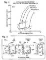
- FIG. 1is a graph showing the relationship between quantum efficiency and the percentage of Ge in a SiGe film.
- FIG. 3is a partial cross-section detailed view of the Si feature sidewall or Si feature surface of FIG. 2 .
- FIGS. 5 through 10illustrate steps in the fabrication of the present invention 3D quantum dot IR optical path structure.
- FIG. 11is a graph depicting an exemplary relationship between the miscut angle and spacing between steps.
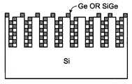
- FIG. 2is a partial cross-sectional view of the present invention 3D quantum dot optical path structure for IR photodetection.
- the structure 200comprises a single-crystal Si substrate 202 with a surface 204 .
- a Si feature 206is formed in the Si substrate surface 204 . More specifically, a via feature 206 a , trench feature 206 b , and pillar feature 206 c are shown.
- a 3D optical path 208 with dots 210 of a first material including germanium (Ge)is formed on Si feature.
- the optical path first material dots 210include a first material of either Ge or SiGe. Alternately stated, the dots have a Ge concentration in the range from 5 to 100%.
- the Si feature 206includes defect sites 212 . The dots 210 are more likely to form in the defect sites than on the feature sidewalls 216 or feature surfaces 214 .
- the Si feature 206has a height 218 that is in the range of 0.3 to 5 microns.
- the substrate 200need not single-crystal Si, especially if the quantum dots 210 are to randomly deposited. However, as explained below, a single-crystal Si substrate permits a controlled number of defect sites to be produced.
- FIG. 3is a partial cross-section detailed view of the Si feature sidewall or Si feature surface of FIG. 2 .
- the Si feature 206is formed along a plane 300 in the substrate with a miscut angle 302 , and includes steps 304 in the Si feature plane responsive to the miscut angle 302 .
- the same miscut angleis typically formed in the sidewall and feature surface.
- the Si feature 206is formed along a plane that is approximately parallel to the substrate surface (substrate surface 204 /feature surface 214 , see FIG. 2 ) and/or approximately normal to the substrate surface (sidewall 212 , see FIG. 2 ).
- the substrate surfacemay also be formed along a plane with a miscut angle.
- the term “approximately” as used hereinis intended to represent a slight deviation of a surface or plane from a perfect crystallographic orientation.
- the steps 304function as a controlled form of defect site to reliable collect dots 210 . Also shown are optical path first material dots 210 formed in the Si feature steps 304 .
- the miscut angle 302is typically in the range between 0.1 and 5 degrees.
- the Si feature 206includes step cross-sections in the Si feature plane responsive to the miscut angle.
- a step cross-sectionas used herein is understood to be the intersection of 2 steps that are formed along two different directions in the same plane.
- a step cross-sectionmight be the intersection of perpendicular steps formed in a Si feature plane.
- the optical path first material dotscan be formed in the Si feature step cross-sections.
- the dotscan be formed in just the step cross-sections, because the free energy of formation at the nucleation sites with cross-sections is lower than other sites.
- deposition conditionsare adjusted to render a higher nuclei density, for example, by increasing the deposition rate or decreasing the deposition temperature, dots can be formed in both the steps and step cross-sections.
- deposition conditions that yield an even higher nuclei densitydots can be deposited indiscriminately on sites between the steps and away from step cross-sections. That is, dots can be formed on defect-free surfaces, as well as surfaces with defects, as a result of the third nuclei density.
- the Si feature 206may be formed along planes in the ( 001 ),
- FIG. 4is a partial cross-sectional view featuring an alternate aspect of the optical path structure 208 of FIG. 2 .
- the optical path 208further includes a Si layer 400 overlying the first material dots 210 formed on the sidewall (surface) 216 ( 214 ) of the Si feature 206 . Then, first material dots 210 are formed on the Si layer 400 .
- first material dots 210are formed on the Si layer 400 .
- only a single layer of Siis shown interposed between the 3D dot levels 402 and 404 , it should be understood that the optical path structure is not limited to any particular number of dot/Si/dot layers.
- FIGS. 5 through 10illustrate steps in the fabrication of the present invention 3D quantum dot IR optical path structure.
- FIG. 5depicts a cross-sectional view of a Si substrate.
- a standard photolithographic techniquecan be used to define the surface of Si.
- a dry etchingis used to etch the Si substrate to a depth of about 1 ⁇ m, for example, to form trench, via, or pillar structures.
- SiGe or Ge quantum dotsare deposited on features.
- the gap 600 between the sidewallscan be as small as 100 nm, and the wall thickness 602 can be in the same range.
- the Si substrate surface, feature surface, and sidewallscan be oriented at an angle from perfect crystallographic orientation, to increase the number of steps on both the horizontal surface and the vertical walls.
- the Si substrate surfacemay be miscut with respect to the ( 100 ) direction. Due to the decrease of energy barrier for nuclei formation, preferred nuclei formation starts at the miscut angle step sites and the cross-section of steps, see FIG. 8 .
- FIG. 9depicts one wall of the trench structure.
- FIG. 10depicts the wall of FIG. 9 following the deposition of Ge (SiGe) dots.
- GeSiGe dots
- these stepsserve as preferential nucleation sites.
- quantum dots deposition sitescan further be limited to the cross-section of steps, where the nucleation free energy is the lowest. Therefore, location and distribution of quantum dots can be controlled.
- FIG. 11is a graph depicting an exemplary relationship between the miscut angle and spacing between steps.
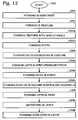
- FIG. 12is a flowchart illustrating the present invention method for selectively forming a 3D quantum dot optical path for IR photodetection. Although the method is depicted as a sequence of numbered steps for clarity, no order should be inferred from the numbering unless explicitly stated. It should be understood that some of these steps may be skipped, performed in parallel, or performed without the requirement of maintaining a strict order of sequence.
- the methodstarts at Step 1200 .
- Step 1202forms a single crystal Si substrate with a surface.
- Step 1204forms a Si feature, such as a via, trench, or pillar in the substrate.
- the Si featuremay have a (sidewall) height in the range of 0.3 to 5 microns.
- Step 1206forms dots of a first material including Ge overlying the Si feature. In some aspects, Step 1206 forms dots having a diameter in the range between 3 and 100 nm.
- Step 1208forms an optical path including first material dots.
- Forming dots of a first material including Ge in Step 1206includes the first material being Ge or SiGe.
- the first materialis SiGe, with a Ge concentration in the range between 5 and 100%.
- Step 1206includes epitaxially growing the first material.
- forming a Si feature in the substrateincludes forming a Si feature in the substrate with defect sites.
- the methodmay rely upon naturally occurring or random defect sites.
- Step 1204includes substeps.
- Step 1204 aforms the Si feature along a plane in the substrate with a miscut angle.
- Forming the Si feature along a plane in the substrate with a miscut angleincludes forming a plane in a direction approximately parallel to the substrate surface and/or approximately normal to the substrate surface.
- Step 1204 aforms a plane with a miscut angle in the range between 0.1 and 5 degrees.
- Step 1204 bin response to the miscut angle, forms steps in the Si feature plane.
- Step 1204 badditionally forms step cross-sections.
- forming dots of a first material overlying the Si featureincludes depositing dots in the Si feature steps and step cross-sections.
- Step 1204 bforms steps with a spacing between steps in the range between 1 and 250 nanometers (nm). The spacing is dependent upon the atomic packing density of the Si substrate.
- Step 1206includes substeps.
- Step 1206 aforms dots overlying the Si feature step cross-sections in response to a first nuclei density.
- Step 1206 bforms dots overlying the Si feature steps in response to a second nuclei density, greater than the first nuclei density.
- Step 1206 cforms dots overlying the Si feature sidewalls and feature steps in response to a third nuclei density, greater than the second nuclei density.
- forming a single crystal Si substrate with a surfaceincludes forming the surface in the ( 001 ) direction. Then, forming a Si feature along a plane (Step 1204 ) includes forming the plane in a direction such as the ( 001 ), ( 100 ), ( 010 ), or ( 110 ) directions. Alternately, if Step 1202 forms the single crystal Si substrate surface in the ( 110 ) or ( 111 ) direction, Step 1204 forms the Si feature along a plane in a direction parallel, or perpendicular to ( 110 ) or ( 111 ) directions, respectively.
- Step 1204forms the Si feature along a plane either parallel or perpendicular to the ( 110 ) direction. Likewise, if Step 1202 forms the substrate in the ( 111 ) direction, Step 1204 forms the Si feature along a plane either parallel or perpendicular to the ( 111 ) direction.
- Step 1208forming an optical path including first material dots in Step 1208 includes substeps.
- Step 1208 adeposits a Si layer overlying the first material dots.
- Step 1208 bforms first material dots on the Si layer.
Landscapes
- Engineering & Computer Science (AREA)
- Chemical & Material Sciences (AREA)
- Nanotechnology (AREA)
- Physics & Mathematics (AREA)
- Crystallography & Structural Chemistry (AREA)
- Mathematical Physics (AREA)
- Theoretical Computer Science (AREA)
- Life Sciences & Earth Sciences (AREA)
- Biophysics (AREA)
- Optics & Photonics (AREA)
- Light Receiving Elements (AREA)
Abstract
Description
- This application is a continuation-in-part of a pending patent application entitled, SURFACE-NORMAL OPTICAL PATH STRUCTURE FOR INFRARED PHOTODETECTION, invented by Lee et al., Ser. No. ______, filed ______, attorney docket no. SLA826.
- This application is a continuation-in-part of a pending patent application entitled, VERTICAL OPTICAL PATH STRUCTURE FOR INFRARED PHOTODETECTION, invented by Tweet et al., Ser. No. ______, filed ______, attorney docket no. SLA831.
- 1. Field of the Invention
- This invention generally relates to integrated circuit (IC) fabrication processes and, more particularly, to a quantum dot three-dimensional optical path structure and corresponding fabrication method.
- 2. Description of the Related Art
- There are many applications for photodetection in the near infrared region (the wavelength between 0.7 micron to 2 microns), such as in fiber-optical communication, security, and thermal imaging. Although III-V compound semiconductors provide superior optical performance over their silicon (Si)-based counterparts, the use of Si is desirable, as the compatibility of Si-based materials with conventional Si—IC technology promises the possibility of cheap, small, and highly integrated optical systems.
- Silicon photodiodes are widely used as photodetectors in the visible light wavelengths due to their low dark current and the above-mentioned compatibility with Si IC technologies. Further, silicon-germanium (Si1-xGex) permits the photodetection of light in the 0.8 to 1.6 micron wavelength region.
- However, the SiGe alloy has larger lattice constant than the Si lattice, so film thickness is a critical variable in the epitaxial growth of SiGe on Si substrates. While a thick SiGe is desirable for light absorption, too thick of a SiGe film causes a defect generation that is responsible for dark currents. This critical SiGe thickness is dependent upon the Ge concentration and device process temperature. Higher Ge concentrations and higher device process temperatures result in the formation of thinner SiGe film thicknesses. In common practice, the SiGe critical thickness is in the range of a few hundred angstroms, to maximum of a few thousand angstroms. Once the SiGe thickness is grown beyond its critical thickness, lattice defects in SiGe are inevitable. As mentioned above, an IR photo detector built from a SiGe film with lattice defects generates large dark currents and noise.
- Quantum efficiency is a measure of the number of electron-hole pairs generated per incident photon, and it is a parameter for photodetector sensitivity. Quantum efficiency is defined as:
η=(Ip/q)/(Popt/hv) - where Ipis the current generated by the absorption of incident optical power Poptat the light frequency v.
FIG. 1 is a graph showing the relationship between quantum efficiency and the percentage of Ge in a SiGe film. One of the key factors in determining quantum efficiency is the absorption coefficient, α. Silicon has a cutoff wavelength of about 1.1 microns and is transparent in the wavelength region between 1.3 to 1.6 microns. The SiGe absorption edge shifts to the red with an increasing Ge mole fraction and is shown inFIG. 1 . The absorption coefficient of any SiGe alloy is relatively small and the limited thickness dictated by the critical thickness further limits the ability of SiGe films to absorb photons.- As noted above, the major goals of SiGe-based photodetection are high quantum efficiency and the integration of these SiGe photodetectors with the existing Si electronics. One way to increase the optical path, and improve the quantum efficiency, is to form the optical path in the same plane as the SiGe film, along the substrate surface in which the SiGe is deposited. Thus, light propagates parallel to the heterojunction (SiGe/Si) interface. However, this optical path design necessarily limits the design of IR detectors.
- The IR absorption length of SiGe is long and thus a thick SiGe layer, greater than 1 micron for example, is required to achieve high IR absorption and high quantum efficiency. However, it is very difficult to grow a defect-free thick SiGe film on a Si substrate because of the lattice mismatch between these two materials. As described in pending application SURFACE-NORMAL OPTICAL PATH STRUCTURE FOR INFRARED PHOTODETECTION, which is incorporated herein by reference, a long SiGe optical path can be formed without necessarily forming a thick SiGe film. By growing the SiGe film on the sidewall of a Si trench or pillar, any IR light entering the device and traveling along the sidewall, encounters a long optical path. A long optical path improves the quantum efficiency.
- However, growing the SiGe by a blanket deposition technique results in SiGe growth on the bottom of the trenches and top of the wafer, as well as on the sidewalls. Although SiGe has a larger lattice constant than Si, it can be grown lattice-matched to Si, up to the so-called critical thickness. Consequently, SiGe grown on the sidewalls has the Si lattice constant parallel to the sidewalls, but a larger lattice constant perpendicular to them. At the same time, the SiGe grown at the bottom of the trenches and top of the wafer has the Si lattice constant parallel to those surfaces, but a larger one perpendicular to them. Crystals originating from these different surfaces consequently have defected regions where they meet.
- Large two-dimensional focal plane arrays in the mid- and far-infrared region can also be made using compound semiconductors such as indium antimonide or mercury cadmium telluride detector arrays bonded to a Si chip for multiplexing. However, this approach is expensive and difficult. Another method is to use quantum well infrared photodetectors (QWIP). But QWIPs are insensitive to normal incident light.
- To overcome the above-mentioned limitations associated with two-dimensional structures, and to extend performance to near-infrared range of the spectrum, stress-induced quantum dots have been considered for use in a quantum dot infrared detector (QDIP). The size and distribution of the quantum dots are controlled in accordance with the Stranski-Krastanow heteroepitaxy growth mode, using a lattice mismatch between the film and the substrate material. Two-dimensional arrays of quantum dots may be formed using lithographic techniques to form a thin dielectric pattern. Beam irradiations and thermal etching techniques are also known. A multilayer quantum dot structure can also be formed by first depositing the multiple layers, followed by a heat treatment step to induce an agglomeration process to form the quantum dots. Other techniques form colloidal nanocrystals through sintering on porous template. However, these 2D quantum dot processes are relatively complex.
- To avoid the above-mentioned problems inherent with a two-dimensional interface between films, it would be advantageous if a long length SiGe optical path structure could be formed using a three-dimensional array of SiGe quantum dots.
- The present invention is a three-dimensional quantum dot structure formed from a simple one-layer deposition, using surface relief aspects of the substrate. With a pre-arranged substrate orientation, the precise location of quantum dots, as well as their size and distribution, can be reliably controlled. Therefore, an IR detector of improved spectral sensitivity and reproducibility can be fabricated.
- Accordingly, a method is provided for selectively forming a three-dimensional quantum dot optical path for IR photodetection. The method comprises: forming a single crystal Si substrate with a surface; forming a Si feature in the substrate, such as a via, trench, or pillar; forming dots from a Ge or SiGe material overlying the Si feature; and, forming an optical path that includes the dots.
- In some aspects of the method, the Si feature has defect sites. For example, the Si feature may be formed along a plane in the substrate with a miscut angle. As a result of the miscut angle, steps are formed in the Si feature plane. Then, the dots are formed in the Si feature steps. The miscut angle is in the range between 0.1 and 5 degrees, and the spacing between steps is in the range between 1 and 250 nanometers (nm). The dots have a diameter in the range between 3 and 100 nm.
- Additional details of the above-described method and a 3D quantum dot optical path structure for IR photodetection are provided below.
FIG. 1 is a graph showing the relationship between quantum efficiency and the percentage of Ge in a SiGe film.FIG. 2 is a partial cross-sectional view of the present invention 3D quantum dot optical path structure for IR photodetection.FIG. 3 is a partial cross-section detailed view of the Si feature sidewall or Si feature surface ofFIG. 2 .FIG. 4 is a partial cross-sectional view featuring an alternate aspect of the optical path structure ofFIG. 2 .FIGS. 5 through 10 illustrate steps in the fabrication of the present invention 3D quantum dot IR optical path structure.FIG. 11 is a graph depicting an exemplary relationship between the miscut angle and spacing between steps.FIG. 12 is a flowchart illustrating the present invention method for selectively forming a 3D quantum dot optical path for IR photodetection.FIG. 2 is a partial cross-sectional view of the present invention 3D quantum dot optical path structure for IR photodetection. Thestructure 200 comprises a single-crystal Si substrate 202 with asurface 204. ASi feature 206 is formed in theSi substrate surface 204. More specifically, a viafeature 206a,trench feature 206b, and pillar feature206care shown. A 3Doptical path 208 withdots 210 of a first material including germanium (Ge) is formed on Si feature.- The optical path
first material dots 210 include a first material of either Ge or SiGe. Alternately stated, the dots have a Ge concentration in the range from 5 to 100%. In one aspect of thestructure 200, the Si feature206 includesdefect sites 212. Thedots 210 are more likely to form in the defect sites than on the feature sidewalls216 or feature surfaces214. The Si feature206 has aheight 218 that is in the range of 0.3 to 5 microns. In other aspects of the invention, thesubstrate 200 need not single-crystal Si, especially if thequantum dots 210 are to randomly deposited. However, as explained below, a single-crystal Si substrate permits a controlled number of defect sites to be produced. FIG. 3 is a partial cross-section detailed view of the Si feature sidewall or Si feature surface ofFIG. 2 . The Si feature206 is formed along aplane 300 in the substrate with amiscut angle 302, and includessteps 304 in the Si feature plane responsive to themiscut angle 302. The same miscut angle is typically formed in the sidewall and feature surface. With respect to a crystallographic direction of (100) for example, the Si feature206 is formed along a plane that is approximately parallel to the substrate surface (substrate surface 204/feature surface 214, seeFIG. 2 ) and/or approximately normal to the substrate surface (sidewall 212, seeFIG. 2 ). However, it should be understood that the substrate surface may also be formed along a plane with a miscut angle. The term “approximately” as used herein is intended to represent a slight deviation of a surface or plane from a perfect crystallographic orientation.- The
steps 304 function as a controlled form of defect site to reliablecollect dots 210. Also shown are optical pathfirst material dots 210 formed in the Si feature steps304. Themiscut angle 302 is typically in the range between 0.1 and 5 degrees. - The Si feature206 also has a
spacing 306 betweensteps 304 that is in the range between 1 and 250 nanometers (nm). The optical pathfirst material dots 210 have adiameter 308 in the range between 3 and 100 nm. Knowing themiscut angle 302, thespacing 306, and thedot diameter 308, the first material density of the optical path structure can be reliably predicted. Alternately stated, the area between dots, or the non-first material density of the optical path structure can be predicted. The spacing306 betweensteps 304 is dependent upon the particular crystallographic orientation of theSi feature plane 300, and also dependent upon the atomic packing density of theSi substrate 200. - In another aspect, the Si feature206 includes step cross-sections in the Si feature plane responsive to the miscut angle. A step cross-section, as used herein is understood to be the intersection of 2 steps that are formed along two different directions in the same plane. For example, a step cross-section might be the intersection of perpendicular steps formed in a Si feature plane. The optical path first material dots can be formed in the Si feature step cross-sections.
- By controlling the conditions associated with the deposition of dots, especially the nuclei density, the dots can be formed in just the step cross-sections, because the free energy of formation at the nucleation sites with cross-sections is lower than other sites. When deposition conditions are adjusted to render a higher nuclei density, for example, by increasing the deposition rate or decreasing the deposition temperature, dots can be formed in both the steps and step cross-sections. With deposition conditions that yield an even higher nuclei density, dots can be deposited indiscriminately on sites between the steps and away from step cross-sections. That is, dots can be formed on defect-free surfaces, as well as surfaces with defects, as a result of the third nuclei density.
- If the single crystal Si substrate surface (204, see
FIG. 2 ) is formed in the (001) direction. TheSi feature 206, considering both sidewalls and feature surface, may be formed along planes in the (001), - (100), (010), or (110) directions. As noted above, the Si feature may have miscut angles that prevent the planes from being perfectly aligned with the above-mentioned crystallographic directions. Likewise, if the single crystal Si substrate surface is formed in the (110) or (111) direction, the Si feature may be formed along a plane in a direction parallel to the (110) or
- (111) directions, respectively, or a plane perpendicular to the (110) or
- (111) directions, respectively.
FIG. 4 is a partial cross-sectional view featuring an alternate aspect of theoptical path structure 208 ofFIG. 2 . In this aspect, theoptical path 208 further includes aSi layer 400 overlying thefirst material dots 210 formed on the sidewall (surface)216 (214) of theSi feature 206. Then,first material dots 210 are formed on theSi layer 400. Although only a single layer of Si is shown interposed between the3D dot levels FIGS. 5 through 10 illustrate steps in the fabrication of the present invention 3D quantum dot IR optical path structure.FIG. 5 depicts a cross-sectional view of a Si substrate. As seen inFIG. 6 , a standard photolithographic technique can be used to define the surface of Si. Then a dry etching is used to etch the Si substrate to a depth of about 1 μm, for example, to form trench, via, or pillar structures. After a proper cleaning, SiGe or Ge quantum dots are deposited on features. The gap600 between the sidewalls can be as small as 100 nm, and the wall thickness602 can be in the same range.- Due to the lattice mismatch, as predicted using Stranski-Krastanow, Ge, or SiGe dots are formed on the vertical sidewalls as well as horizontal (feature surface) areas, see
FIG. 7 . - To further control the sites and the size distribution of the quantum dots, the Si substrate surface, feature surface, and sidewalls, can be oriented at an angle from perfect crystallographic orientation, to increase the number of steps on both the horizontal surface and the vertical walls. For example, the Si substrate surface may be miscut with respect to the (100) direction. Due to the decrease of energy barrier for nuclei formation, preferred nuclei formation starts at the miscut angle step sites and the cross-section of steps, see
FIG. 8 . FIG. 9 depicts one wall of the trench structure. When Si is cut at an angle deviated from (100) axis, the number of surface steps increases with the increase of miscut angle.FIG. 10 depicts the wall ofFIG. 9 following the deposition of Ge (SiGe) dots. During deposition of Ge or SiGe dots, these steps serve as preferential nucleation sites. With proper control of deposition condition, quantum dots deposition sites can further be limited to the cross-section of steps, where the nucleation free energy is the lowest. Therefore, location and distribution of quantum dots can be controlled.FIG. 11 is a graph depicting an exemplary relationship between the miscut angle and spacing between steps.FIG. 12 is a flowchart illustrating the present invention method for selectively forming a 3D quantum dot optical path for IR photodetection. Although the method is depicted as a sequence of numbered steps for clarity, no order should be inferred from the numbering unless explicitly stated. It should be understood that some of these steps may be skipped, performed in parallel, or performed without the requirement of maintaining a strict order of sequence. The method starts atStep 1200.Step 1202 forms a single crystal Si substrate with a surface.Step 1204 forms a Si feature, such as a via, trench, or pillar in the substrate. The Si feature may have a (sidewall) height in the range of 0.3 to 5 microns.Step 1206 forms dots of a first material including Ge overlying the Si feature. In some aspects,Step 1206 forms dots having a diameter in the range between 3 and 100 nm.Step 1208 forms an optical path including first material dots.- Forming dots of a first material including Ge in
Step 1206 includes the first material being Ge or SiGe. Alternately stated, the first material is SiGe, with a Ge concentration in the range between 5 and 100%. In some aspects,Step 1206 includes epitaxially growing the first material. - In some aspects of the method, forming a Si feature in the substrate (Step1204) includes forming a Si feature in the substrate with defect sites. The method may rely upon naturally occurring or random defect sites. Alternately,
Step 1204 includes substeps.Step 1204aforms the Si feature along a plane in the substrate with a miscut angle. Forming the Si feature along a plane in the substrate with a miscut angle (Step1204a) includes forming a plane in a direction approximately parallel to the substrate surface and/or approximately normal to the substrate surface. In other aspects,Step 1204aforms a plane with a miscut angle in the range between 0.1 and 5 degrees. Step 1204b, in response to the miscut angle, forms steps in the Si feature plane. In other aspects,Step 1204badditionally forms step cross-sections. Then, forming dots of a first material overlying the Si feature (Step1206) includes depositing dots in the Si feature steps and step cross-sections. In one aspect,Step 1204bforms steps with a spacing between steps in the range between 1 and 250 nanometers (nm). The spacing is dependent upon the atomic packing density of the Si substrate.- More specifically,
Step 1206 includes substeps.Step 1206aforms dots overlying the Si feature step cross-sections in response to a first nuclei density. Further,Step 1206bforms dots overlying the Si feature steps in response to a second nuclei density, greater than the first nuclei density.Step 1206cforms dots overlying the Si feature sidewalls and feature steps in response to a third nuclei density, greater than the second nuclei density. - In one aspect, forming a single crystal Si substrate with a surface (Step1202) includes forming the surface in the (001) direction. Then, forming a Si feature along a plane (Step1204) includes forming the plane in a direction such as the (001), (100), (010), or (110) directions. Alternately, if
Step 1202 forms the single crystal Si substrate surface in the (110) or (111) direction,Step 1204 forms the Si feature along a plane in a direction parallel, or perpendicular to (110) or (111) directions, respectively. That is, ifStep 1202 forms the substrate in the (110) direction,Step 1204 forms the Si feature along a plane either parallel or perpendicular to the (110) direction. Likewise, ifStep 1202 forms the substrate in the (111) direction,Step 1204 forms the Si feature along a plane either parallel or perpendicular to the (111) direction. - In another aspect, forming an optical path including first material dots in
Step 1208 includes substeps.Step 1208adeposits a Si layer overlying the first material dots.Step 1208bforms first material dots on the Si layer. - A 3D quantum dot optical path structure and corresponding fabrication process have been presented. Simple surface-normal features such as vias, trenches, and pillars have been used to illustrate the invention. However, the invention may also be applied to more complicated features. Likewise, although particular dot dimensions and spacings have been described, the invention is not necessarily limited to these densities. Other variations and embodiments of the invention will occur to those skilled in the art.
Claims (36)
Priority Applications (2)
| Application Number | Priority Date | Filing Date | Title |
|---|---|---|---|
| US10/794,158US6967112B2 (en) | 2003-12-23 | 2004-03-03 | Three-dimensional quantum dot structure for infrared photodetection |
| JP2005058250AJP2005252264A (en) | 2004-03-03 | 2005-03-02 | Three-dimensional quantum dot structure for infrared light detection |
Applications Claiming Priority (3)
| Application Number | Priority Date | Filing Date | Title |
|---|---|---|---|
| US10/746,952US7129488B2 (en) | 2003-12-23 | 2003-12-23 | Surface-normal optical path structure for infrared photodetection |
| US10/755,567US7045832B2 (en) | 2003-12-23 | 2004-01-12 | Vertical optical path structure for infrared photodetection |
| US10/794,158US6967112B2 (en) | 2003-12-23 | 2004-03-03 | Three-dimensional quantum dot structure for infrared photodetection |
Related Parent Applications (1)
| Application Number | Title | Priority Date | Filing Date |
|---|---|---|---|
| US10/755,567Continuation-In-PartUS7045832B2 (en) | 2003-12-23 | 2004-01-12 | Vertical optical path structure for infrared photodetection |
Publications (2)
| Publication Number | Publication Date |
|---|---|
| US20050196894A1true US20050196894A1 (en) | 2005-09-08 |
| US6967112B2 US6967112B2 (en) | 2005-11-22 |
Family
ID=35385025
Family Applications (1)
| Application Number | Title | Priority Date | Filing Date |
|---|---|---|---|
| US10/794,158Expired - LifetimeUS6967112B2 (en) | 2003-12-23 | 2004-03-03 | Three-dimensional quantum dot structure for infrared photodetection |
Country Status (1)
| Country | Link |
|---|---|
| US (1) | US6967112B2 (en) |
Cited By (7)
| Publication number | Priority date | Publication date | Assignee | Title |
|---|---|---|---|---|
| US20050236556A1 (en)* | 2004-04-19 | 2005-10-27 | Edward Sargent | Optically-regulated optical emission using colloidal quantum dot nanocrystals |
| US7742322B2 (en) | 2005-01-07 | 2010-06-22 | Invisage Technologies, Inc. | Electronic and optoelectronic devices with quantum dot films |
| US7746681B2 (en) | 2005-01-07 | 2010-06-29 | Invisage Technologies, Inc. | Methods of making quantum dot films |
| US7773404B2 (en) | 2005-01-07 | 2010-08-10 | Invisage Technologies, Inc. | Quantum dot optical devices with enhanced gain and sensitivity and methods of making same |
| US20110103039A1 (en)* | 2008-03-13 | 2011-05-05 | Nxp B.V. | Luminescent component and manufacturing method |
| US8115232B2 (en) | 2005-01-07 | 2012-02-14 | Invisage Technologies, Inc. | Three-dimensional bicontinuous heterostructures, a method of making them, and their application in quantum dot-polymer nanocomposite photodetectors and photovoltaics |
| CN103903966A (en)* | 2014-03-11 | 2014-07-02 | 复旦大学 | Method for manufacturing ultrahigh-density germanium silicon quantum dots based on obliquely-cut silicon substrate |
Families Citing this family (6)
| Publication number | Priority date | Publication date | Assignee | Title |
|---|---|---|---|---|
| US9685524B2 (en) | 2005-03-11 | 2017-06-20 | Vishay-Siliconix | Narrow semiconductor trench structure |
| TWI489557B (en)* | 2005-12-22 | 2015-06-21 | Vishay Siliconix | High-mobility P-channel trench and planar vacant mode power metal oxide semiconductor field effect transistor |
| US8409954B2 (en) | 2006-03-21 | 2013-04-02 | Vishay-Silconix | Ultra-low drain-source resistance power MOSFET |
| WO2007112088A2 (en)* | 2006-03-24 | 2007-10-04 | Qd Vision, Inc. | Hyperspectral imaging device |
| WO2009002551A1 (en)* | 2007-06-26 | 2008-12-31 | Qd Vision, Inc. | Photovoltaic devices including quantum dot down-conversion materials useful for solar cells and materials including quantum dots |
| US9412883B2 (en) | 2011-11-22 | 2016-08-09 | Taiwan Semiconductor Manufacturing Company, Ltd. | Methods and apparatus for MOS capacitors in replacement gate process |
Citations (12)
| Publication number | Priority date | Publication date | Assignee | Title |
|---|---|---|---|---|
| US5229320A (en)* | 1991-08-02 | 1993-07-20 | Sony Corporation | Method for forming quantum dots |
| US5482890A (en)* | 1994-10-14 | 1996-01-09 | National Science Council | Method of fabricating quantum dot structures |
| US5614435A (en)* | 1994-10-27 | 1997-03-25 | The Regents Of The University Of California | Quantum dot fabrication process using strained epitaxial growth |
| US5683595A (en)* | 1995-03-31 | 1997-11-04 | Shimadzu Corporation | Fine pattern forming method and fine pattern device |
| US6139626A (en)* | 1998-09-04 | 2000-10-31 | Nec Research Institute, Inc. | Three-dimensionally patterned materials and methods for manufacturing same using nanocrystals |
| US6242326B1 (en)* | 1998-12-02 | 2001-06-05 | Electronics And Telecommunications Research Institute | Method for fabricating compound semiconductor substrate having quantum dot array structure |
| US6333214B1 (en)* | 1998-06-29 | 2001-12-25 | Hynix Semiconductor Inc. | Memory of multilevel quantum dot structure and method for fabricating the same |
| US6346431B1 (en)* | 2000-07-10 | 2002-02-12 | Lg Electronics Inc. | Quantum dot infrared detection device and method for fabricating the same |
| US6541788B2 (en)* | 1998-10-27 | 2003-04-01 | The Regents Of The University Of California | Mid infrared and near infrared light upconverter using self-assembled quantum dots |
| US6632694B2 (en)* | 2001-10-17 | 2003-10-14 | Astralux, Inc. | Double heterojunction light emitting diodes and laser diodes having quantum dot silicon light emitters |
| US20040053469A1 (en)* | 2002-09-17 | 2004-03-18 | Sung-Eon Park | Method for forming quantum dot |
| US20040152225A1 (en)* | 2003-02-04 | 2004-08-05 | Industrial Technology Research Institute | Method for fabricating multiple thickness insulator layers |
- 2004
- 2004-03-03USUS10/794,158patent/US6967112B2/ennot_activeExpired - Lifetime
Patent Citations (12)
| Publication number | Priority date | Publication date | Assignee | Title |
|---|---|---|---|---|
| US5229320A (en)* | 1991-08-02 | 1993-07-20 | Sony Corporation | Method for forming quantum dots |
| US5482890A (en)* | 1994-10-14 | 1996-01-09 | National Science Council | Method of fabricating quantum dot structures |
| US5614435A (en)* | 1994-10-27 | 1997-03-25 | The Regents Of The University Of California | Quantum dot fabrication process using strained epitaxial growth |
| US5683595A (en)* | 1995-03-31 | 1997-11-04 | Shimadzu Corporation | Fine pattern forming method and fine pattern device |
| US6333214B1 (en)* | 1998-06-29 | 2001-12-25 | Hynix Semiconductor Inc. | Memory of multilevel quantum dot structure and method for fabricating the same |
| US6139626A (en)* | 1998-09-04 | 2000-10-31 | Nec Research Institute, Inc. | Three-dimensionally patterned materials and methods for manufacturing same using nanocrystals |
| US6541788B2 (en)* | 1998-10-27 | 2003-04-01 | The Regents Of The University Of California | Mid infrared and near infrared light upconverter using self-assembled quantum dots |
| US6242326B1 (en)* | 1998-12-02 | 2001-06-05 | Electronics And Telecommunications Research Institute | Method for fabricating compound semiconductor substrate having quantum dot array structure |
| US6346431B1 (en)* | 2000-07-10 | 2002-02-12 | Lg Electronics Inc. | Quantum dot infrared detection device and method for fabricating the same |
| US6632694B2 (en)* | 2001-10-17 | 2003-10-14 | Astralux, Inc. | Double heterojunction light emitting diodes and laser diodes having quantum dot silicon light emitters |
| US20040053469A1 (en)* | 2002-09-17 | 2004-03-18 | Sung-Eon Park | Method for forming quantum dot |
| US20040152225A1 (en)* | 2003-02-04 | 2004-08-05 | Industrial Technology Research Institute | Method for fabricating multiple thickness insulator layers |
Cited By (24)
| Publication number | Priority date | Publication date | Assignee | Title |
|---|---|---|---|---|
| US20050236556A1 (en)* | 2004-04-19 | 2005-10-27 | Edward Sargent | Optically-regulated optical emission using colloidal quantum dot nanocrystals |
| US7326908B2 (en)* | 2004-04-19 | 2008-02-05 | Edward Sargent | Optically-regulated optical emission using colloidal quantum dot nanocrystals |
| US9054246B2 (en) | 2004-04-19 | 2015-06-09 | Invisage Technologies, Inc. | Quantum dot optical devices with enhanced gain and sensitivity and methods of making same |
| US9570502B2 (en) | 2004-04-19 | 2017-02-14 | Invisage Technologies, Inc. | Quantum dot optical devices with enhanced gain and sensitivity and methods of making same |
| US9806131B2 (en) | 2004-04-19 | 2017-10-31 | Invisage Technologies, Inc. | Quantum dot optical devices with enhanced gain and sensitivity and methods of making same |
| US9373736B2 (en) | 2004-04-19 | 2016-06-21 | Invisage Technologies, Inc. | Quantum dot optical devices with enhanced gain and sensitivity and methods of making same |
| US8115232B2 (en) | 2005-01-07 | 2012-02-14 | Invisage Technologies, Inc. | Three-dimensional bicontinuous heterostructures, a method of making them, and their application in quantum dot-polymer nanocomposite photodetectors and photovoltaics |
| US8284586B2 (en) | 2005-01-07 | 2012-10-09 | Invisage Technologies, Inc. | Electronic and optoelectronic devices with quantum dot films |
| US8054671B2 (en) | 2005-01-07 | 2011-11-08 | Invisage Technologies, Inc. | Methods of making quantum dot films |
| US8102693B2 (en) | 2005-01-07 | 2012-01-24 | Invisage Technologies, Inc. | Quantum dot optical devices with enhanced gain and sensitivity and methods of making same |
| US7881091B2 (en) | 2005-01-07 | 2011-02-01 | InVisage Technologies. Inc. | Methods of making quantum dot films |
| US8213212B2 (en) | 2005-01-07 | 2012-07-03 | Invisage Technologies, Inc. | Methods of making quantum dot films |
| US8284587B2 (en) | 2005-01-07 | 2012-10-09 | Invisage Technologies, Inc. | Quantum dot optical devices with enhanced gain and sensitivity and methods of making same |
| US8023306B2 (en) | 2005-01-07 | 2011-09-20 | Invisage Technologies, Inc. | Electronic and optoelectronic devices with quantum dot films |
| US7773404B2 (en) | 2005-01-07 | 2010-08-10 | Invisage Technologies, Inc. | Quantum dot optical devices with enhanced gain and sensitivity and methods of making same |
| US8422266B2 (en) | 2005-01-07 | 2013-04-16 | Invisage Technologies, Inc. | Quantum dot optical devices with enhanced gain and sensitivity and methods of making same |
| US8450138B2 (en) | 2005-01-07 | 2013-05-28 | Invisage Technologies, Inc. | Three-dimensional bicontinuous heterostructures, method of making, and their application in quantum dot-polymer nanocomposite photodetectors and photovoltaics |
| US8724366B2 (en) | 2005-01-07 | 2014-05-13 | Invisage Technologies, Inc. | Quantum dot optical devices with enhanced gain and sensitivity and methods of making same |
| US7746681B2 (en) | 2005-01-07 | 2010-06-29 | Invisage Technologies, Inc. | Methods of making quantum dot films |
| US7742322B2 (en) | 2005-01-07 | 2010-06-22 | Invisage Technologies, Inc. | Electronic and optoelectronic devices with quantum dot films |
| US9231223B2 (en) | 2005-01-07 | 2016-01-05 | Invisage Technologies, Inc. | Three-dimensional bicontinuous heterostructures, method of making, and their application in quantum dot-polymer nanocomposite photodetectors and photovoltaics |
| US20110103039A1 (en)* | 2008-03-13 | 2011-05-05 | Nxp B.V. | Luminescent component and manufacturing method |
| US8376801B2 (en) | 2008-03-13 | 2013-02-19 | Nxp B.V. | Luminescent component and manufacturing method |
| CN103903966A (en)* | 2014-03-11 | 2014-07-02 | 复旦大学 | Method for manufacturing ultrahigh-density germanium silicon quantum dots based on obliquely-cut silicon substrate |
Also Published As
| Publication number | Publication date |
|---|---|
| US6967112B2 (en) | 2005-11-22 |
Similar Documents
| Publication | Publication Date | Title |
|---|---|---|
| US7045832B2 (en) | Vertical optical path structure for infrared photodetection | |
| US7361526B2 (en) | Germanium photo detector having planar surface through germanium epitaxial overgrowth | |
| Lei et al. | Progress, challenges, and opportunities for HgCdTe infrared materials and detectors | |
| US7297564B1 (en) | Fabrication of vertical sidewalls on (110) silicon substrates for use in Si/SiGe photodetectors | |
| TWI482299B (en) | Nanowire structure photodiode having a P or N layer surrounded by epitaxial growth | |
| US6967112B2 (en) | Three-dimensional quantum dot structure for infrared photodetection | |
| TW201205643A (en) | Dislocation and stress management by mask-less processes using substrate patterning and methods for device fabrication | |
| US9490318B2 (en) | Three dimensional strained semiconductors | |
| TW201143055A (en) | Nanowire photo-detector grown on a back-side illuminated image sensor | |
| TWI518925B (en) | A photovoltaic element device having a surface periodic grating structure and a method of manufacturing the same | |
| JP2016129225A (en) | Semiconductor light-receiving device and semiconductor light-receiving element | |
| Falub et al. | 3D heteroepitaxy of mismatched semiconductors on silicon | |
| US20060189151A1 (en) | Method for forming an infrared photodetector with a vertical optical path | |
| JP2017220648A (en) | Semiconductor crystal substrate, infrared ray detection device, manufacturing method of semiconductor crystal substrate, and manufacturing method of infrared ray detection device | |
| JP6769486B2 (en) | Manufacturing method of semiconductor crystal substrate, manufacturing method of infrared detector | |
| US11069825B2 (en) | Optoelectronic devices formed over a buffer | |
| US11251320B2 (en) | Photodetector structures formed on high-index substrates | |
| JP2005252264A (en) | Three-dimensional quantum dot structure for infrared light detection | |
| RU220600U1 (en) | Heterostructural photodiode for the near and mid-IR range based on indium arsenide-phosphide-bismuthide nanocrystals on silicon substrates | |
| JP2012119567A (en) | Method of manufacturing semiconductor wafer, method of manufacturing semiconductor device, and method of manufacturing sensor array | |
| Liu | Germanium-Tin on Silicon for Integrated Photonics and Integrated Quantum Materials | |
| KR100790020B1 (en) | Diffusion Method Used in the Manufacturing Process of Avalanche Photodetectors | |
| Huang | Gallium nitride-based and high-speed metal-semiconductor-metal photodetector: Growth and device structures for integration |
Legal Events
| Date | Code | Title | Description |
|---|---|---|---|
| AS | Assignment | Owner name:SHARP LABORATORIES OF AMERICA, INC., WASHINGTON Free format text:ASSIGNMENT OF ASSIGNORS INTEREST;ASSIGNORS:MAA, JER-SHEN;LEE, JONG-JAN;TWEET, DOUGLAS J.;AND OTHERS;REEL/FRAME:015064/0501 Effective date:20040302 | |
| STCF | Information on status: patent grant | Free format text:PATENTED CASE | |
| FPAY | Fee payment | Year of fee payment:4 | |
| FPAY | Fee payment | Year of fee payment:8 | |
| FEPP | Fee payment procedure | Free format text:PAYER NUMBER DE-ASSIGNED (ORIGINAL EVENT CODE: RMPN); ENTITY STATUS OF PATENT OWNER: LARGE ENTITY Free format text:PAYOR NUMBER ASSIGNED (ORIGINAL EVENT CODE: ASPN); ENTITY STATUS OF PATENT OWNER: LARGE ENTITY | |
| AS | Assignment | Owner name:SHARP KABUSHIKI KAISHA, JAPAN Free format text:ASSIGNMENT OF ASSIGNORS INTEREST;ASSIGNOR:SHARP LABORATORIES OF AMERICA, INC.;REEL/FRAME:035208/0580 Effective date:20150319 | |
| AS | Assignment | Owner name:SHARP KABUSHIKI KAISHA AKA SHARP CORPORATION, JAPA Free format text:NUNC PRO TUNC ASSIGNMENT;ASSIGNOR:SHARP LABORATORIES OF AMERICA, INC.;REEL/FRAME:039973/0978 Effective date:20150319 | |
| FPAY | Fee payment | Year of fee payment:12 | |
| AS | Assignment | Owner name:MICROSOFT TECHNOLOGY LICENSING, LLC, WASHINGTON Free format text:ASSIGNMENT OF ASSIGNORS INTEREST;ASSIGNOR:SHARP CORPORATION AKA SHARP KABUSHIKI KAISHA;REEL/FRAME:044410/0751 Effective date:20150715 |