US20050194672A1 - Stacked packages and systems incorporating the same - Google Patents
Stacked packages and systems incorporating the sameDownload PDFInfo
- Publication number
- US20050194672A1 US20050194672A1US10/981,067US98106704AUS2005194672A1US 20050194672 A1US20050194672 A1US 20050194672A1US 98106704 AUS98106704 AUS 98106704AUS 2005194672 A1US2005194672 A1US 2005194672A1
- Authority
- US
- United States
- Prior art keywords
- unit
- terminals
- stack
- interposer
- units
- Prior art date
- Legal status (The legal status is an assumption and is not a legal conclusion. Google has not performed a legal analysis and makes no representation as to the accuracy of the status listed.)
- Granted
Links
Images


Classifications
- H—ELECTRICITY
- H01—ELECTRIC ELEMENTS
- H01L—SEMICONDUCTOR DEVICES NOT COVERED BY CLASS H10
- H01L25/00—Assemblies consisting of a plurality of semiconductor or other solid state devices
- H01L25/03—Assemblies consisting of a plurality of semiconductor or other solid state devices all the devices being of a type provided for in a single subclass of subclasses H10B, H10D, H10F, H10H, H10K or H10N, e.g. assemblies of rectifier diodes
- H01L25/10—Assemblies consisting of a plurality of semiconductor or other solid state devices all the devices being of a type provided for in a single subclass of subclasses H10B, H10D, H10F, H10H, H10K or H10N, e.g. assemblies of rectifier diodes the devices having separate containers
- H—ELECTRICITY
- H01—ELECTRIC ELEMENTS
- H01L—SEMICONDUCTOR DEVICES NOT COVERED BY CLASS H10
- H01L23/00—Details of semiconductor or other solid state devices
- H01L23/48—Arrangements for conducting electric current to or from the solid state body in operation, e.g. leads, terminal arrangements ; Selection of materials therefor
- H01L23/488—Arrangements for conducting electric current to or from the solid state body in operation, e.g. leads, terminal arrangements ; Selection of materials therefor consisting of soldered or bonded constructions
- H01L23/498—Leads, i.e. metallisations or lead-frames on insulating substrates, e.g. chip carriers
- H01L23/49833—Leads, i.e. metallisations or lead-frames on insulating substrates, e.g. chip carriers the chip support structure consisting of a plurality of insulating substrates
- H—ELECTRICITY
- H01—ELECTRIC ELEMENTS
- H01L—SEMICONDUCTOR DEVICES NOT COVERED BY CLASS H10
- H01L23/00—Details of semiconductor or other solid state devices
- H01L23/48—Arrangements for conducting electric current to or from the solid state body in operation, e.g. leads, terminal arrangements ; Selection of materials therefor
- H01L23/488—Arrangements for conducting electric current to or from the solid state body in operation, e.g. leads, terminal arrangements ; Selection of materials therefor consisting of soldered or bonded constructions
- H01L23/498—Leads, i.e. metallisations or lead-frames on insulating substrates, e.g. chip carriers
- H01L23/4985—Flexible insulating substrates
- H—ELECTRICITY
- H01—ELECTRIC ELEMENTS
- H01L—SEMICONDUCTOR DEVICES NOT COVERED BY CLASS H10
- H01L24/00—Arrangements for connecting or disconnecting semiconductor or solid-state bodies; Methods or apparatus related thereto
- H01L24/01—Means for bonding being attached to, or being formed on, the surface to be connected, e.g. chip-to-package, die-attach, "first-level" interconnects; Manufacturing methods related thereto
- H01L24/10—Bump connectors ; Manufacturing methods related thereto
- H01L24/15—Structure, shape, material or disposition of the bump connectors after the connecting process
- H01L24/17—Structure, shape, material or disposition of the bump connectors after the connecting process of a plurality of bump connectors
- H—ELECTRICITY
- H01—ELECTRIC ELEMENTS
- H01L—SEMICONDUCTOR DEVICES NOT COVERED BY CLASS H10
- H01L25/00—Assemblies consisting of a plurality of semiconductor or other solid state devices
- H01L25/03—Assemblies consisting of a plurality of semiconductor or other solid state devices all the devices being of a type provided for in a single subclass of subclasses H10B, H10D, H10F, H10H, H10K or H10N, e.g. assemblies of rectifier diodes
- H01L25/10—Assemblies consisting of a plurality of semiconductor or other solid state devices all the devices being of a type provided for in a single subclass of subclasses H10B, H10D, H10F, H10H, H10K or H10N, e.g. assemblies of rectifier diodes the devices having separate containers
- H01L25/105—Assemblies consisting of a plurality of semiconductor or other solid state devices all the devices being of a type provided for in a single subclass of subclasses H10B, H10D, H10F, H10H, H10K or H10N, e.g. assemblies of rectifier diodes the devices having separate containers the devices being integrated devices of class H10
- H—ELECTRICITY
- H05—ELECTRIC TECHNIQUES NOT OTHERWISE PROVIDED FOR
- H05K—PRINTED CIRCUITS; CASINGS OR CONSTRUCTIONAL DETAILS OF ELECTRIC APPARATUS; MANUFACTURE OF ASSEMBLAGES OF ELECTRICAL COMPONENTS
- H05K1/00—Printed circuits
- H05K1/02—Details
- H05K1/11—Printed elements for providing electric connections to or between printed circuits
- H05K1/111—Pads for surface mounting, e.g. lay-out
- H05K1/112—Pads for surface mounting, e.g. lay-out directly combined with via connections
- H—ELECTRICITY
- H01—ELECTRIC ELEMENTS
- H01L—SEMICONDUCTOR DEVICES NOT COVERED BY CLASS H10
- H01L2224/00—Indexing scheme for arrangements for connecting or disconnecting semiconductor or solid-state bodies and methods related thereto as covered by H01L24/00
- H01L2224/01—Means for bonding being attached to, or being formed on, the surface to be connected, e.g. chip-to-package, die-attach, "first-level" interconnects; Manufacturing methods related thereto
- H01L2224/10—Bump connectors; Manufacturing methods related thereto
- H01L2224/15—Structure, shape, material or disposition of the bump connectors after the connecting process
- H01L2224/16—Structure, shape, material or disposition of the bump connectors after the connecting process of an individual bump connector
- H01L2224/161—Disposition
- H01L2224/16151—Disposition the bump connector connecting between a semiconductor or solid-state body and an item not being a semiconductor or solid-state body, e.g. chip-to-substrate, chip-to-passive
- H01L2224/16221—Disposition the bump connector connecting between a semiconductor or solid-state body and an item not being a semiconductor or solid-state body, e.g. chip-to-substrate, chip-to-passive the body and the item being stacked
- H01L2224/16225—Disposition the bump connector connecting between a semiconductor or solid-state body and an item not being a semiconductor or solid-state body, e.g. chip-to-substrate, chip-to-passive the body and the item being stacked the item being non-metallic, e.g. insulating substrate with or without metallisation
- H—ELECTRICITY
- H01—ELECTRIC ELEMENTS
- H01L—SEMICONDUCTOR DEVICES NOT COVERED BY CLASS H10
- H01L2225/00—Details relating to assemblies covered by the group H01L25/00 but not provided for in its subgroups
- H01L2225/03—All the devices being of a type provided for in the same main group of the same subclass of class H10, e.g. assemblies of rectifier diodes
- H01L2225/04—All the devices being of a type provided for in the same main group of the same subclass of class H10, e.g. assemblies of rectifier diodes the devices not having separate containers
- H01L2225/065—All the devices being of a type provided for in the same main group of the same subclass of class H10
- H01L2225/06503—Stacked arrangements of devices
- H01L2225/0652—Bump or bump-like direct electrical connections from substrate to substrate
- H—ELECTRICITY
- H01—ELECTRIC ELEMENTS
- H01L—SEMICONDUCTOR DEVICES NOT COVERED BY CLASS H10
- H01L2225/00—Details relating to assemblies covered by the group H01L25/00 but not provided for in its subgroups
- H01L2225/03—All the devices being of a type provided for in the same main group of the same subclass of class H10, e.g. assemblies of rectifier diodes
- H01L2225/04—All the devices being of a type provided for in the same main group of the same subclass of class H10, e.g. assemblies of rectifier diodes the devices not having separate containers
- H01L2225/065—All the devices being of a type provided for in the same main group of the same subclass of class H10
- H01L2225/06503—Stacked arrangements of devices
- H01L2225/06527—Special adaptation of electrical connections, e.g. rewiring, engineering changes, pressure contacts, layout
- H—ELECTRICITY
- H01—ELECTRIC ELEMENTS
- H01L—SEMICONDUCTOR DEVICES NOT COVERED BY CLASS H10
- H01L2225/00—Details relating to assemblies covered by the group H01L25/00 but not provided for in its subgroups
- H01L2225/03—All the devices being of a type provided for in the same main group of the same subclass of class H10, e.g. assemblies of rectifier diodes
- H01L2225/04—All the devices being of a type provided for in the same main group of the same subclass of class H10, e.g. assemblies of rectifier diodes the devices not having separate containers
- H01L2225/065—All the devices being of a type provided for in the same main group of the same subclass of class H10
- H01L2225/06503—Stacked arrangements of devices
- H01L2225/06548—Conductive via connections through the substrate, container, or encapsulation
- H—ELECTRICITY
- H01—ELECTRIC ELEMENTS
- H01L—SEMICONDUCTOR DEVICES NOT COVERED BY CLASS H10
- H01L2225/00—Details relating to assemblies covered by the group H01L25/00 but not provided for in its subgroups
- H01L2225/03—All the devices being of a type provided for in the same main group of the same subclass of class H10, e.g. assemblies of rectifier diodes
- H01L2225/04—All the devices being of a type provided for in the same main group of the same subclass of class H10, e.g. assemblies of rectifier diodes the devices not having separate containers
- H01L2225/065—All the devices being of a type provided for in the same main group of the same subclass of class H10
- H01L2225/06503—Stacked arrangements of devices
- H01L2225/06572—Auxiliary carrier between devices, the carrier having an electrical connection structure
- H—ELECTRICITY
- H01—ELECTRIC ELEMENTS
- H01L—SEMICONDUCTOR DEVICES NOT COVERED BY CLASS H10
- H01L2225/00—Details relating to assemblies covered by the group H01L25/00 but not provided for in its subgroups
- H01L2225/03—All the devices being of a type provided for in the same main group of the same subclass of class H10, e.g. assemblies of rectifier diodes
- H01L2225/10—All the devices being of a type provided for in the same main group of the same subclass of class H10, e.g. assemblies of rectifier diodes the devices having separate containers
- H01L2225/1005—All the devices being of a type provided for in the same main group of the same subclass of class H10, e.g. assemblies of rectifier diodes the devices having separate containers the devices being integrated devices of class H10
- H01L2225/1011—All the devices being of a type provided for in the same main group of the same subclass of class H10, e.g. assemblies of rectifier diodes the devices having separate containers the devices being integrated devices of class H10 the containers being in a stacked arrangement
- H01L2225/1017—All the devices being of a type provided for in the same main group of the same subclass of class H10, e.g. assemblies of rectifier diodes the devices having separate containers the devices being integrated devices of class H10 the containers being in a stacked arrangement the lowermost container comprising a device support
- H01L2225/1023—All the devices being of a type provided for in the same main group of the same subclass of class H10, e.g. assemblies of rectifier diodes the devices having separate containers the devices being integrated devices of class H10 the containers being in a stacked arrangement the lowermost container comprising a device support the support being an insulating substrate
- H—ELECTRICITY
- H01—ELECTRIC ELEMENTS
- H01L—SEMICONDUCTOR DEVICES NOT COVERED BY CLASS H10
- H01L2225/00—Details relating to assemblies covered by the group H01L25/00 but not provided for in its subgroups
- H01L2225/03—All the devices being of a type provided for in the same main group of the same subclass of class H10, e.g. assemblies of rectifier diodes
- H01L2225/10—All the devices being of a type provided for in the same main group of the same subclass of class H10, e.g. assemblies of rectifier diodes the devices having separate containers
- H01L2225/1005—All the devices being of a type provided for in the same main group of the same subclass of class H10, e.g. assemblies of rectifier diodes the devices having separate containers the devices being integrated devices of class H10
- H01L2225/1011—All the devices being of a type provided for in the same main group of the same subclass of class H10, e.g. assemblies of rectifier diodes the devices having separate containers the devices being integrated devices of class H10 the containers being in a stacked arrangement
- H01L2225/1047—Details of electrical connections between containers
- H01L2225/107—Indirect electrical connections, e.g. via an interposer, a flexible substrate, using TAB
- H—ELECTRICITY
- H01—ELECTRIC ELEMENTS
- H01L—SEMICONDUCTOR DEVICES NOT COVERED BY CLASS H10
- H01L23/00—Details of semiconductor or other solid state devices
- H01L23/48—Arrangements for conducting electric current to or from the solid state body in operation, e.g. leads, terminal arrangements ; Selection of materials therefor
- H01L23/488—Arrangements for conducting electric current to or from the solid state body in operation, e.g. leads, terminal arrangements ; Selection of materials therefor consisting of soldered or bonded constructions
- H01L23/498—Leads, i.e. metallisations or lead-frames on insulating substrates, e.g. chip carriers
- H01L23/49811—Additional leads joined to the metallisation on the insulating substrate, e.g. pins, bumps, wires, flat leads
- H01L23/49816—Spherical bumps on the substrate for external connection, e.g. ball grid arrays [BGA]
- H—ELECTRICITY
- H01—ELECTRIC ELEMENTS
- H01L—SEMICONDUCTOR DEVICES NOT COVERED BY CLASS H10
- H01L24/00—Arrangements for connecting or disconnecting semiconductor or solid-state bodies; Methods or apparatus related thereto
- H01L24/01—Means for bonding being attached to, or being formed on, the surface to be connected, e.g. chip-to-package, die-attach, "first-level" interconnects; Manufacturing methods related thereto
- H01L24/10—Bump connectors ; Manufacturing methods related thereto
- H01L24/12—Structure, shape, material or disposition of the bump connectors prior to the connecting process
- H01L24/14—Structure, shape, material or disposition of the bump connectors prior to the connecting process of a plurality of bump connectors
- H—ELECTRICITY
- H01—ELECTRIC ELEMENTS
- H01L—SEMICONDUCTOR DEVICES NOT COVERED BY CLASS H10
- H01L25/00—Assemblies consisting of a plurality of semiconductor or other solid state devices
- H01L25/03—Assemblies consisting of a plurality of semiconductor or other solid state devices all the devices being of a type provided for in a single subclass of subclasses H10B, H10D, H10F, H10H, H10K or H10N, e.g. assemblies of rectifier diodes
- H01L25/04—Assemblies consisting of a plurality of semiconductor or other solid state devices all the devices being of a type provided for in a single subclass of subclasses H10B, H10D, H10F, H10H, H10K or H10N, e.g. assemblies of rectifier diodes the devices not having separate containers
- H01L25/065—Assemblies consisting of a plurality of semiconductor or other solid state devices all the devices being of a type provided for in a single subclass of subclasses H10B, H10D, H10F, H10H, H10K or H10N, e.g. assemblies of rectifier diodes the devices not having separate containers the devices being of a type provided for in group H10D89/00
- H01L25/0655—Assemblies consisting of a plurality of semiconductor or other solid state devices all the devices being of a type provided for in a single subclass of subclasses H10B, H10D, H10F, H10H, H10K or H10N, e.g. assemblies of rectifier diodes the devices not having separate containers the devices being of a type provided for in group H10D89/00 the devices being arranged next to each other
- H—ELECTRICITY
- H01—ELECTRIC ELEMENTS
- H01L—SEMICONDUCTOR DEVICES NOT COVERED BY CLASS H10
- H01L2924/00—Indexing scheme for arrangements or methods for connecting or disconnecting semiconductor or solid-state bodies as covered by H01L24/00
- H01L2924/10—Details of semiconductor or other solid state devices to be connected
- H01L2924/11—Device type
- H01L2924/14—Integrated circuits
- H01L2924/143—Digital devices
- H01L2924/1434—Memory
- H01L2924/1435—Random access memory [RAM]
- H01L2924/1437—Static random-access memory [SRAM]
- H—ELECTRICITY
- H01—ELECTRIC ELEMENTS
- H01L—SEMICONDUCTOR DEVICES NOT COVERED BY CLASS H10
- H01L2924/00—Indexing scheme for arrangements or methods for connecting or disconnecting semiconductor or solid-state bodies as covered by H01L24/00
- H01L2924/15—Details of package parts other than the semiconductor or other solid state devices to be connected
- H01L2924/151—Die mounting substrate
- H01L2924/153—Connection portion
- H01L2924/1531—Connection portion the connection portion being formed only on the surface of the substrate opposite to the die mounting surface
- H01L2924/15311—Connection portion the connection portion being formed only on the surface of the substrate opposite to the die mounting surface being a ball array, e.g. BGA
- H—ELECTRICITY
- H05—ELECTRIC TECHNIQUES NOT OTHERWISE PROVIDED FOR
- H05K—PRINTED CIRCUITS; CASINGS OR CONSTRUCTIONAL DETAILS OF ELECTRIC APPARATUS; MANUFACTURE OF ASSEMBLAGES OF ELECTRICAL COMPONENTS
- H05K1/00—Printed circuits
- H05K1/02—Details
- H05K1/14—Structural association of two or more printed circuits
- H05K1/141—One or more single auxiliary printed circuits mounted on a main printed circuit, e.g. modules, adapters
- H—ELECTRICITY
- H05—ELECTRIC TECHNIQUES NOT OTHERWISE PROVIDED FOR
- H05K—PRINTED CIRCUITS; CASINGS OR CONSTRUCTIONAL DETAILS OF ELECTRIC APPARATUS; MANUFACTURE OF ASSEMBLAGES OF ELECTRICAL COMPONENTS
- H05K2201/00—Indexing scheme relating to printed circuits covered by H05K1/00
- H05K2201/10—Details of components or other objects attached to or integrated in a printed circuit board
- H05K2201/10227—Other objects, e.g. metallic pieces
- H05K2201/10378—Interposers
- H—ELECTRICITY
- H05—ELECTRIC TECHNIQUES NOT OTHERWISE PROVIDED FOR
- H05K—PRINTED CIRCUITS; CASINGS OR CONSTRUCTIONAL DETAILS OF ELECTRIC APPARATUS; MANUFACTURE OF ASSEMBLAGES OF ELECTRICAL COMPONENTS
- H05K2201/00—Indexing scheme relating to printed circuits covered by H05K1/00
- H05K2201/10—Details of components or other objects attached to or integrated in a printed circuit board
- H05K2201/10431—Details of mounted components
- H05K2201/10507—Involving several components
- H05K2201/10515—Stacked components
- H—ELECTRICITY
- H05—ELECTRIC TECHNIQUES NOT OTHERWISE PROVIDED FOR
- H05K—PRINTED CIRCUITS; CASINGS OR CONSTRUCTIONAL DETAILS OF ELECTRIC APPARATUS; MANUFACTURE OF ASSEMBLAGES OF ELECTRICAL COMPONENTS
- H05K3/00—Apparatus or processes for manufacturing printed circuits
- H05K3/30—Assembling printed circuits with electric components, e.g. with resistor
- H05K3/32—Assembling printed circuits with electric components, e.g. with resistor electrically connecting electric components or wires to printed circuits
- H05K3/34—Assembling printed circuits with electric components, e.g. with resistor electrically connecting electric components or wires to printed circuits by soldering
- H05K3/341—Surface mounted components
- H05K3/3431—Leadless components
- H05K3/3436—Leadless components having an array of bottom contacts, e.g. pad grid array or ball grid array components
Definitions
- the present inventionrelates to microelectronic packaging and systems.
- Microelectronic elementssuch as semiconductor chips are commonly provided in packages having terminals connected to the microelectronic element itself, such terminals being available for connection to external elements such as printed circuit boards.
- microelectronic elementsnotably memory chips
- Some microelectronic elementshave been provided heretofore in stacked arrangements with packages superposed one atop the other to conserve space on a circuit board.
- Such structurestypically involve only a few chips and relatively simple connections which normally do not involve interconnections between chips in the stack, or between multiple stacks of chips. Even in these situations, it is sometimes necessary to provide different packages for different chips in the stack.
- One aspect of the present inventionprovides a stacked packaging arrangement especially useful for, e.g., logic chips such as field programmable gate arrays (hereinafter “FPGA”) or microprocessors, in which the stacked packaging arrangement accommodates logical interconnections between chips where inputs from one chip are connected to outputs of other chips.
- FPGAfield programmable gate arrays
- a further aspect of the inventionprovides designs for individual units and elements which can be used in such stacked arrangement.
- Yet another aspect of the inventionprovides a system-level design which allows for integration of multiple stacked packages while minimizing the complexity of signal routing in a printed circuit board (“PCB”) or other circuit panel used in the system.
- PCBprinted circuit board
- Still other aspects of the inventionprovide unit configurations which facilitate routing of signals to chips on different packages in a stack.
- FIG. 1is a diagrammatic top plan view of a unit in accordance with one embodiment of the invention.
- FIG. 2is a diagrammatic bottom plan view of the unit shown in FIG. 1 .
- FIG. 3is a fragmentary, diagrammatic elevational view showing a portion of an assembly including the unit of FIGS. 1 and 2 .
- FIG. 4is a diagrammatic perspective view of the assembly depicted in FIG. 3 .
- FIG. 5is a fragmentary, diagrammatic, sectional view taken along line 5 - 5 in FIG. 4 .
- FIG. 6is a diagrammatic top elevational view of a component used in the assembly of FIGS. 3-5 .
- FIG. 7is a fragmentary, partially schematic sectional view showing a portion of the unit depicted in FIG. 1 .
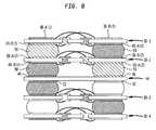
- FIG. 8is a fragmentary, diagrammatic elevational view showing a portion of the assembly depicted in FIGS. 3-5 , with certain components omitted for clarity of illustration.
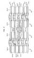
- FIG. 9is a view similar to FIG. 8 , but depicting a further portion of the assembly.
- FIG. 10is a view similar to FIGS. 8 and 9 , but depicting yet a further portion of the assembly.
- FIG. 11is a further fragmentary, diagrammatic elevational view depicting yet another portion of the same assembly.
- FIG. 12is a diagrammatic sectional view depicting a unit in accordance with a further embodiment of the invention.
- FIG. 13is a fragmentary, diagrammatic sectional view depicting a portion of an assembly including units as shown in FIG. 12 .
- FIG. 14is a diagrammatic top plan view of a portion of a memory assembly.
- FIG. 15is a fragmentary, diagrammatic sectional view depicting a portion of a unit in accordance with a further embodiment of the invention.
- FIG. 16is a diagrammatic elevational view depicting an assembly incorporating a plurality of units as shown in FIG. 15 .
- FIG. 17is a diagrammatic top plan view depicting a unit in accordance with yet another embodiment of the invention.
- FIG. 18is a diagrammatic elevational view depicting an assembly incorporating units as shown in FIG. 17 .
- a systemuses a plurality of units 30 ( FIGS. 1 and 2 ).
- Each unitincludes a unit substrate 32 in the form of a dielectric element such as a circuit board or flexible circuit panel, commonly referred to as a “tape.”
- the unit substratedefines a top side 34 ( FIG. 1 ) and a bottom side 36 ( FIG. 2 ).
- Each unit substratehas top unit terminals 38 exposed at the top side of the unit and bottom unit terminals 40 exposed at its bottom side.
- Each unitalso includes a first microelectronic element in the form of a semiconductor chip 41 , in this case, an FPGA.
- each unitalso includes additional semiconductor chips or SRAMs 43 .
- the SRAM within each unitcooperates with the FPGA of that particular unit.
- the FPGA chipis flip-chip mounted to the top of the unit substrate, so that the unit substrate serves as the package for the FPGA.
- the SRAMsare supplied in separate chip size packages, which are LGA-bonded to the bottom side of the unit substrate. Any other chip mounting techniques can be used.
- terminals 38 and 40are solderable lands.
- Each unithas vertical directions from the top to the bottom and has horizontal directions transverse to the vertical directions. Thus, the horizontal directions extend parallel to the planes of the top and bottom of the unit.
- a horizontal direction to the left as seen in FIG. 1is referred to herein as the “north” direction (“N”); whereas an orthogonal horizontal direction, to the bottom of the drawing in FIG. 1 , is referred to herein as the “west” direction (“W”).
- the top terminals 38 and the bottom terminals 40are disposed in positions referred to herein as column positions. Terminals at the same column position on a given unit are disposed at the same position in the horizontal directions of the unit.
- each unit substratemay be a ceramic or other chip carrier having a pocket or hole arranged to receive the chip or chips and having contacts on top and bottom sides of the substrate.
- the chipitself can be provided with terminals on its top and bottom sides, so that each unit consists only of the chip.
- some or all of the terminals on the top and bottom sides of the substratemay be formed by common elements.
- a terminal in the form of a pad disposed on one surface of the substratemay be exposed to the opposite surface of the substrate through a hole in the substrate, so that the same pad defines terminals exposed at both sides of the substrate.
- the SRAM chips incorporated within each unitcooperate with the FPGA of such unit. Each unit incorporates appropriate connections (not shown) between the SRAM and the FPGA.
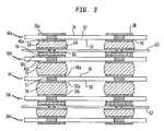
- the unitsare arranged in four stacks ( 42 - 0 , 42 - 1 , 42 - 2 and 42 - 3 ).
- Each stackincludes four units superposed, one above the other.
- stack 42 - 0includes units 30 A, 30 b , 30 c and 30 d ).
- the four stacks of four unitsthus provide 16 units and 16 FPGAs in all.
- the systemalso includes a printed circuit board 44 .
- circuit board 44is shown as a transparent plane outlined by a solid black line in FIG. 4 .
- FIG. 4As best seen in FIG.
- circuit panel 44is a multilayer circuit board including several layers of dielectric material and internal conductors (not shown), as well as other conventional elements commonly found in a circuit board.
- Circuit board 44has an upper surface 46 with upper pads 48 exposed at such upper surface, and has an oppositely directed lower surface 50 with lower pads 52 exposed at lower surface 50 .
- two units of each stacklie above PCB 44 , whereas two units lie below the PCB.
- units 30 a and 30 blie above the PCB
- units 30 c and 30 dlie below the PCB. All of the units within each stack have the same orientation.
- Units 30 a and 30 bdisposed above PCB 44 , have their top sides 34 facing upwardly, away from the PCB, whereas units 30 a and 30 b , disposed below the plane of the PCB, also have their top sides 30 c and 30 d facing upwardly; but in this case, the top sides face toward the PCB. Also, within a single stack, all of the units have their horizontal directions oriented in the same way.
- the internal structures of all of the units in each stack, and indeed all of the units in all of the stacks,are identical to one another. The ability to use identical units, desirably without modification of individual units, greatly reduces the number of different components which must be handled and stocked, and thus reduces the cost of the assembly.
- the units within each stackare aligned with one another in their horizontal directions, so that terminals on all of the units in the same column position are vertically superposed above one another. Stated another way, a vertical line drawn through a terminal at a particular column position on one unit will pass through all of the other terminals at the same column position on the other units in the stack.
- the terminals of all of the units within the stackare connected so that all of the terminals disposed at the same column position are connected to one another and connected to the printed circuit board.
- a “normal stack connection”referred to as a “normal stack connection” and shown in FIG. 3
- the top terminal at each position on a given unitis electrically connected to the bottom terminal at the same position on the same unit.
- the bottom terminal at each positionis electrically connected by one or more conductive elements to the top terminal of the next lower unit at the same position.
- top terminal 38 ais connected to the bottom terminal 40 a of the same unit 30 a , and in turn, electrically connected to top terminal 38 b of the next lower unit 30 b.
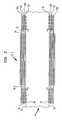
- interposers 60 and 62extend between portions of the units in each stack.
- interposer 60 and 62themselves are configured as circuit panels with terminals on their top and bottom surfaces. At those column positions where normal or straight-through connections are desired, interposers 60 and 62 have pairs of terminals aligned with one another and connected to one another, as exemplified by terminals 64 and 66 on interposer 60 in FIG. 3 . These terminals simply form part of the conductive connection between the bottom terminal 40 on each unit and the top terminal 38 b on the next lower unit in the stack at the same column position.
- the conductive connectionsdesirably include conductive bonding materials such as solder masses.
- a solder mass 68connects lower terminal 40 a to the corresponding terminals 64 on the top surface of interposer 60
- a further solder elementsuch as a relatively thin solder layer 70 connects terminal 66 of the interposer to the top terminal 38 b of second unit 30 b in the stack.
- printed circuit board 44has a pair of upper and lower pads 48 and 52 referred to herein as a “common pair.”
- One such common pairincludes pads 48 a and 52 a ( FIG. 3 ).
- Pads 48 a and 52 aare substantially aligned with one another, so that upper pad 48 a lies directly above lower pad 52 a at the same column position.
- These padsare electrically connected to one another by a conductor 72 extending through the printed circuit board.
- conductor 72is a simple via extending straight through all of the layers (not shown) of the printed circuit board.
- the conductor connecting the pads of a common pairmay include horizontal or zigzag portions, as required to route the connection around other conductors in the printed circuit board.
- a straight or nearly straight-through vertical conductoris preferred.
- the common pair of pads on the circuit board and the conductor connecting these padsforms part of a conductive connection at the column position between the units above the PCB and the units below the PCB.
- the bottom unit terminal 40 b on the second unit 30 b in the stack, immediately above the PCB,is connected to the upper pad 48 a of the common pair by a further conductive element such as a solder ball 74 ; whereas the lower pad 52 a of the common pair is connected by another conductive element such as a solder ball 76 to the top unit terminal 38 c on the third unit 30 c , disposed immediately below the printed circuit board.
- This configurationis repeated at all column positions where a normal or a straight-through connection extending through the entire stack is desired.
- the ability to make connections between portions of the stack above and below the printed circuit board using a relatively simple, desirably straight connection through the boardgreatly simplifies the board layout.
- the upper interconnect interposer 60is a large circuit panel, such as a rigid or flexible circuit board.
- the interconnect interposerincludes four holes 78 - 0 through 78 - 3 extending through the panel from its top surface to its bottom surface.
- the interconnect interposerfurther includes an array of top interposer terminals 64 surrounding each hole on the top side of the interconnect interposer. Each such array of terminals includes terminals at the same column positions as the terminals of the individual units in one stack.
- Interposer 60also has a corresponding array of bottom interposer terminals ( 66 ; FIG. 3 ) on its bottom surface.
- Upper interposer 60desirably has conductive connections such as traces 80 extending between the various terminal arrays, and particularly, between the mutually adjacent edges of the various terminal arrays. These are shown only schematically in FIG. 6 . These traces are connected to selected ones of the top and bottom terminals to interconnect the stacks with one another, as further discussed below.
- the upper interposer 60intersects all four of the stacks, as does the lower interposer. Only a portion of the interconnect interposer or mezzanine interposer is seen in FIG. 5 .
- One array of top interposer terminals 64 and the corresponding array of bottom interposer terminals 66FIG.
- hole 78 - 0is disposed in alignment with the unit terminals of the units in stack 42 - 0 , whereas hole 78 - 0 is aligned with the chips of the units in stack 42 - 0 so that the chips are received in the hole.
- the top and bottom interposer terminals 64 and 66 at the same column positionare electrically connected to one another so that the interconnect interposer acts as a straight pass-through and does not affect the normal connection arrangement.
- the upper interposeracts as a spacer between the two units of the stack disposed above. This arrangement permits the use of relatively small solder balls. Stated another way, with the mezzanine interposer, the height of each individual solder ball may be less than the aggregate height of the SRAM 43 ( FIG. 2 ) on the bottom of one unit and the FPGA 41 ( FIG. 1 ) on the top of the next lower unit.
- the use of small solder ballsis advantageous, in that it allows the use of relatively small diameter terminals, which conserves space on the surfaces of the units.
- the upper interposer 60is connected in each of the other stacks 42 - 1 through 42 - 3 in the same manner.
- the lower interposer( 62 ; FIGS. 4 and 5 ) is configured similarly to the upper interposer, and also intercepts all four of the stacks in the same way as the upper interposer.
- the lower interposer 62performs exactly the same spacing function with respect to the units disposed below the PCB.
- the various first microelectronic elements or FPGAs 41 located within the stacksare interconnected with one another. At each such interconnection, an output of one FPGA is connected to an input of another FPGA.
- the internal structure of every unitis identical to the individual structure of every other unit. For example, each unit has a top terminal at a given column position connected to an output or contact of the FPGA chip itself. Likewise, each unit has a top terminal at another position, connected to an input pad on the FPGA of the unit. Thus, connecting all of the terminals at the same column position within a particular stack to one another would not connect inputs to outputs, but instead would short inputs together and short outputs together.
- Each unithas a set of terminals, referred to herein as “A” terminals.
- This set of terminalsincludes a top terminal 38 -A disposed at a first column position. Like all of the other top terminals 38 , this terminal (also referred to as a “top A terminal”) is exposed at the top surface 34 of unit substrate 32 .
- the set of A terminalsalso includes one of the bottom unit terminals 40 , referred to herein as a bottom A terminal 40 -A, exposed at the bottom surface 36 at a second column position.
- each unitalso includes a set of “B” terminals.
- This setincludes a top B terminal 38 -B exposed at the second column position, and hence lying directly above the bottom terminal 40 -A.
- the set of B terminalsalso includes a bottom B terminal 40 -B exposed on the bottom surface of the unit substrate at the first column position, directly below the top A terminal 38 -A.
- These B terminalsare interconnected to one another as by via 86 -B and associated traces 88 -B. For clarity of illustration, the traces shown are shown in FIG. 7 as arcuate lines.
- the first microelectronic element or FPGA 41 in each unithas an output or A pad electrically connected to the A terminals and an input or B pad electrically connected to the B terminals.
- the A and B terminalstypically are connected to the A and B pads respectively by traces extending along the top surface of the substrate, but any other form of connection may be used.
- top and bottom terminals on adjacent units in the stack disposed at the same column positionare connected to one another by conductive elements 90 .
- Conductive elements 90are depicted as simple solder ball interconnects in FIG. 8 .
- these conductive interconnectsmay include top and bottom terminals of interposers 60 and 62 as discussed above.
- the interposer terminalssimply form part of the conductive connection between a bottom unit terminal on one unit and the top unit terminal at the same column position on the unit immediately below.
- the interposersare omitted in FIG. 8 for clarity of illustration.
- the bottom A terminal 40 -A( 1 ) of the top-most unit 30 - 1is connected to the top B terminal 38 -B( 2 )of the next lower unit 30 - 2 .
- the bottom B terminal of the top-most unit 30 - 1is connected to the top A terminal 38 -A( 2 ) of the next lower unit 30 - 2 .
- the A terminals of each unitare connected to the B terminals of the adjacent unit, so that the output or A pad of the FPGA 41 ( FIG. 7 ) in each of these two units is connected to the input or B pad of the FPGA 41 ( FIG. 7 ) in the other one of these units.
- the connectionsare carried down to upper pads 48 on the PCB.
- connectionsare not necessary for interchange of information between the units.
- the conductive connections between the lower unit 30 - 2 and pads 48could be omitted, but preferably are used so as to avoid the need for special solder ball arrangements at different locations within the stack.
- the PCB 44can be provided with traces so that these signals can be accessed from outside the stack. At these column positions, the PCB does not connect through to the other units ( 30 - 3 and 30 - 4 ) of the stack, below the PCB. These other units, however, are connected to one another in exactly the same way as units 30 - 1 and 30 - 2 are connected to one another.
- connection discussed with reference to FIGS. 7 and 8provides conductive paths which cross between column positions.
- one such conductive pathextends at a first column position at terminal 38 -A( 1 ) at the top of the stack and then at a second column position (at terminals 40 -A( 1 ) and 38 -B( 2 ) in the middle of the stack, and then crosses again back to the back to the first column position at terminal 40 -B( 2 ) and the associated upper pad 48 of the substrate.
- the other crossed conductive pathstarts at the second column position at terminal 38 -B( 1 ), crosses to the first column position in the middle of the stack at terminals 40 -B( 1 ) and 38 -A( 2 ), and then crosses back again to the second column position at terminals 40 -A( 2 ) and the associated pad 48 on the printed circuit board.
- These conductive pathsare shaded differently in FIG. 8 for clarity of illustration. Similar crossing conductive paths exist in the lower portion of the stack, below the printed circuit board. In this embodiment, the crossing pair of conductive paths is applied to allow connections from inputs to outputs on different units, even though both units have the identical structure. Other applications for crossing conductive paths are discussed below. In this regard, it should be noted that the crossing conductive paths depicted in FIGS.
- connection traces which are used to provide the crossingwould be longer when the column positions used for a pair of crossing conductive paths are not adjacent to one another.
- a stackmay include any number of crossings. Thus, an individual pair of conductive paths may cross one another once or more than once along the vertical extent of the stack.
- each unitincludes a set of A terminals and a set of B terminals at first and second column positions CP 1 and CP 2 in exactly the same arrangement as discussed above with reference to FIGS. 7 and 8 .
- each unitalso includes a set of C terminals and a set of D terminals at third and fourth column positions.
- the C terminals and D terminalsare configured in a manner similar to the A and B terminals.
- the C terminals on unit 30 - 1include a top C terminal 38 -C( 1 ) at third column position CP 3 and a bottom C terminal 40 -C( 1 ) at fourth column position CP 4 , the C terminals being electrically connected to one another.
- the D terminals on this unitinclude a top D terminal 38 -D( 1 ) at fourth column position CP 4 and a bottom D terminal 40 -D( 1 ) at the third column position CP 3 .
- the D terminalsare electrically connected to one another by other traces and vias.
- the A terminalsare connected to an output pad of the first microelectronic element or FPGA.
- the B terminalsare not connected to a pad of the FPGA.
- the C terminalsare connected to an input pad of the FPGA carried by the unit, whereas the D terminals are not connected to a pad of the FPGA.
- the bottom terminals of each unitare connected to the top terminals of the next adjacent unit, except that the bottom terminals of second unit 30 - 2 are connected to the upper pads 48 of PCB 44 disposed at the same column positions, whereas the top terminals of unit 30 - 3 , disposed immediately below the PCB 44 , are connected to the lower pads 52 of the PCB at the same column positions.
- the upper pad 48 at each column position of the first through fourth column position shown in FIG. 9is connected to the lower pad 52 of the circuit board at another column position at these first through fourth positions.
- the upper pad 48 -U 1 at the first column position CP 1is connected to the lower pad 52 -L 3 at the third column position.
- the output connectionis carried from the A terminals 38 -A( 1 ) and 40 -A( 1 ) of top unit 30 - 1 down through terminals 38 -B( 2 ) and 40 -B( 2 ) to upper pad 48 -U 1 at first column position CP 1 , (shaded in FIG. 9 ) and routed along the PCB down to the lower pad 52 -L 3 at the third column position.
- the solder ball below this PCB padconnects to the top C terminal 38 -C( 3 ) on unit 30 - 3 immediately below the PCB, and hence connects to the input pad of the FPGA in that unit.
- the connectioncontinues down through the bottom C terminal 40 -C( 3 ) at the fourth column position, but the solder ball below that bottom C terminal connects to a D terminal 38 -D( 4 )on the top of bottom unit 30 - 4 , and hence, does not connect to the FPGA of this unit.
- the conductive pathconnects to a B terminal 38 -B( 2 ) on the second unit 30 - 2 but does not make a connection to the FPGA of that unit, because the B terminals are not connected.
- the output of the FPGA in top unit 30 - 1is connected only to the input of the FPGA in third unit 30 - 3 in the same stack.
- the PCBalso has an upper pad 48 -U 2 at the second column position CP 2 connected to a lower pad 52 -L 4 at the fourth column position CP 4 .
- the output of unit 30 - 2is connected through these upper and lower pads on the PCB and through the other units to terminal 30 -C( 4 ) of unit 30 - 4 .
- the PCBhas a lower pad 52 -L( 1 ) at the first column position CP 1 connected to an upper pad 48 -U 3 at the third column position CP 3 , and also has a lower pad 52 -L 2 at the second column position CP 2 connected to an upper pad 48 -U 4 at the fourth column position CP 4 .
- the lower pad 52 -L 1 at the first column positionin conjunction with the conductive paths defined by the units, connect the A terminals, and hence the FPGA output contact of unit 30 - 3 to the C terminals, and hence the FPGA input, of unit 30 - 1 .
- the lower pad 52 -L 2 at the second column position and upper pad 48 -U 4 at the fourth column positionserve to connect the A terminals, and hence the FPGA output contact of unit 30 - 4 to the C terminals, and FPGA input contact of unit 30 - 2 .
- each stackthere are unique connections between the units of the stack and the printed circuit board. That is, a signal is routed from the PCB to only one unit in the stack.
- top terminals 38 and bottom terminals 40are provided on each unit at a set of four column positions CP 1 through CP 4 as shown in FIG. 10 .
- these column positionsare depicted as physically adjacent to one another for clarity of illustration, but need not be physically adjacent to one another.
- each unithas a bottom terminal and a top terminal.
- each top terminal 38is connected to the bottom terminal 40 in the next-higher column position of the set.
- the bottom terminal 40 - 4 ( 4 ) on unit 4 at the fourth column position CP 4is electrically connected to the top terminal 38 - 3 ( 4 ) of the same unit in the third column position.
- These connectionscan be made, for example, by traces 88 and vias 86 .
- the top terminal 38 at the highest-ordered column position CP 4 of the setis electrically connected to the bottom terminal 40 at the lowest-ordered column position of the set, as by further traces 87 and via 89 .
- the tracesare schematically indicated by lines shown extending above and below the planes of the unit substrates, but in practice these connections typically extend along the surfaces of the substrate or within the substrate. As seen in FIG.
- the electrical connectionsrun in a stair-step fashion, traversing over one column position at each unit.
- the electrical connectionstraverse the shaded elements, including terminals 40 - 4 ( 4 ) and 38 - 3 ( 4 ) on unit 30 - 4 ; 40 - 3 ( 3 ) and 38 - 2 ( 3 ) on unit 30 - 3 ; 40 - 2 ( 2 ) and 38 - 1 ( 2 ) on unit 30 - 2 ; and 40 - 1 ( 1 ) on unit 30 - 1 .
- each conductive pathextends in a stair-step fashion, moving one column position towards the highest-ordered column position of the set (towards CP 4 ) as it moves down one unit in the stack and, conversely, moving one column position toward the lowest-ordered column position (towards CP 1 ) as it moves up one unit in the stack.
- Each unithas a connection between a particular contact (not shown) on a microelectronic element and the bottom terminal 40 at a particular column, position, in this case the first column position.
- the first microelectronic element or FPGA 41 of unit 30 - 1has a contact connected to terminal 40 - 1 ( 1 ); the same contact on the first microelectronic element or FPGA of unit 30 - 2 is connected to bottom terminal 40 - 1 ( 2 ) of unit 30 - 2 .
- unit 30 - 3has the same contact on the microelectronic element connected to bottom terminal 40 - 1 ( 3 )
- unit 30 - 4 at the bottom of the stackhas the same contact pad of the microelectronic element connected to terminals 40 - 1 ( 4 ).
- the other top and bottom terminals at column positions CP 1 -CP 4are not connected to the microelectronic elements of the various units.
- a circuit board 44 ′ positioned at the bottom of the stackmay have four unique pads 48 ′- 1 through 48 ′- 4 connected to these unique terminals. For example, a signal supplied from the PCB at pad 48 ′- 4 in the fourth column position CP 4 will pass to bottom terminal 40 - 1 ( 1 ) in the first column position of UNIT 30 - 1 . Similarly, the signal supplied through at the second column position through pad 48 ′- 2 (also shaded), will pass to the identical terminal 40 - 1 ( 3 ) on the bottom surface of unit 30 - 3 .
- each conductive pathruns to the highest-ordered column position at top of the unit where the connection reaches the lowest-ordered column position.
- the conductive path from terminal 40 - 3 ( 4 ), at the third column position on the bottom of unit 30 - 4runs up to bottom terminal 40 - 1 ( 2 ) at CP 1 on unit 30 - 2 , and then to top terminal 38 - 4 ( 2 ) at CP 4 on the same unit 30 - 2 .
- the conductive paththus connects to bottom terminal 40 - 4 ( 1 ) on the bottom of unit 30 - 1 and thus to top terminal 38 - 3 ( 1 ) at CP 3 , on the top of the top unit 30 - 1 .
- each of the conductive pathsextends through all four of the units, and ultimately returns to the same column position as it had at the bottom of the stack.
- the “stair-step” arrangementis topologically similar to a spiral staircase; in connection involving a set of N column positions, the arrangement repeats after N units.
- units having such a spiral connectioncan be stacked more than N units high, so that some or all of the conductive paths connect to more than one unit.
- FIG. 10depicts four units disposed on the same side of the PCB. In the embodiment illustrated in the other figures, two units within each stack are disposed on the top and two units are disposed on the bottom, as indicated by the PCB 44 shown in broken lines in FIG. 10 .
- each conductive pathpasses through all of the units (at different column positions), the conductive paths will still connect to unique pads on a circuit board 44 at the location depicted in broken lines.
- pads on a top interposer shown in broken lines at 60 ′ or a bottom interposer 62 ′can also be connected to unique conductive paths.
- the interposer or circuit board used in such an arrangementdesirably has top and bottom pads directly connected to one another as discussed above in connection with FIG. 3 .
- only two column positionsneed be occupied by the stair-step set of column positions to provide unique connections to each of the units, provided that the PCB has separate pads on its top and bottom surfaces.
- the connection between the top pad at the highest-ordered column position and the bottom pad at the lowest-ordered column position(as defined by traces 87 and via 89 in FIG. 10 ) can be omitted.
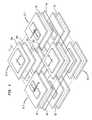
- each stackis disposed in a grid, so that each stack has a side facing a side of another stack.
- a side of stack 42 - 0faces a side of stack 42 - 1
- another side of stack 42 - 0faces a side of stack 42 - 3 .
- two of the stacksare inverted relative to two of the other stacks.
- stack 42 - 1points upwardly relative to the PCB (upwardly in the drawing), whereas the top of stack 42 - 0 points upwardly relative to the PCB 44 .
- Stack 42 - 2has its top facing upwardly
- stack 42 - 3has its bottom facing upwardly.
- stack 42 - 2is rotated 180° relative to stack 42 - 0 about a vertical axis
- stack 42 - 3is rotated 180° relative to stack 42 - 1 .
- the net effectis that corresponding sides of the stacks face one another.
- the terminals which require inter-stack connectionsare placed along the westerly and northerly sides of the stacks.
- the upper interposer 60is provided with connection lines 80 ( FIG. 6 ) interconnecting terminals associated with the various stacks. Very short interconnect lines can connect terminals associated with the northerly edge of stack 42 - 3 and the northerly edge of stack 42 - 0 , and similar short connection lines will connect the westerly edge of stack 42 - 0 with the westerly edge of stack 42 - 1 , and so on.
- the top interposerhas a set of top terminals 64 - 1 and 64 - 2 associated with column positions CP 1 and CP 2 of stack 42 - 0 , for example, on the westerly edge of stack 42 - 0 , electrically connected by traces 80 - 1 and 80 - 2 to corresponding top terminals 64 - 3 and 64 - 4 , at column positions CP 3 and CP 4 on the westerly edge of stack 1 .
- each unithas top and bottom terminals 38 and 40 at the same column position directly connected to one another, as discussed above with reference to FIG. 3 .
- each unit 30has its terminals 38 and 40 connected to an input pad of the FPGA or first microelectronic element.
- each unithas its terminals 38 and 40 connected to an output pad of the FPGA within that unit.
- the terminals at column positions CP 2are connected to an output pad of the FPGA, whereas the terminals on the various units at column positions CP 4 are connected to an input pad of the FPGA.
- the output from the FPGA in unit 30 - 1 - 0 in stack 42 - 0is connected to the input of the FPGA in unit 30 - 1 - 1 in stack 42 - 1 , and other connections are made in similar fashion.
- the top interposer 60has a similar set of bottom terminals 66 and associated traces, which interconnect other units in the two stacks with one another in the same manner.
- the bottom terminals 66 and associated traces used for this functionare electrically isolated from the top terminals 64 and associated traces 80 - 1 and 80 - 2 . Stated another way, at these column positions, the mezzanine interposer does not provide an interconnection between the units in a single stack.
- the bottom interposer 62is arranged in a similar fashion.
- the PCBcan be greatly simplified. Further, packaging each FPGA with its associated SRAMs also avoids the needs for traces on the PCB for interconnecting FPGAs with SRAMs.
- the PCBthus, can have many fewer layers than would be required otherwise.
- a conventional PCB with four FPGAs mounted directly on the PCB, and with SRAMs connected to the FPGAs through the printed circuit board itselfrequires a printed circuit board with more than 25 layers.
- Such a circuit boardis extraordinarily complex, and hence suffers significantly in cost and reliability.
- the design as discussed abovecan accommodate 16 FPGAs and 32 SRAMs in the same circuit board area or less, using a PCB having fewer layers.
- the mezzanine interposermay be provided with A and B pads at first and second column positions, as discussed above with reference to FIGS. 7 and 8 so as to interchange signals between column positions in the interconnect interposer.
- the top and bottom terminals of each unit at each column positionmay be directly connected to one another in the manner shown at FIG. 3 , or else may be formed as parts of the same metallic pad. This can be used, for example, where the unit substrate has only a single layer of metal.
- an arrangement utilizing a stack with portions disposed above and below a printed circuit board or other circuit panel, also referred to as a “mirrored” stackis advantageous in and of itself, even where only one stack is used.
- a stack height on each side of the printed circuit boardcooling of the individual dies is greatly facilitated.
- this resultis achieved without the use of special “mirror image” sets of chips.
- the conductive elements 90are mounted on the top surfaces of the various units disposed below the circuit board, whereas the conductive elements are mounted on the bottom surfaces of the units disposed below the circuit board.
- the same arrangementcan be used with any stackable units having terminals on its top and bottom surfaces, with or without the other features discussed above.
- chips other than FPGAsmay be utilized.
- the number of chips per unit, the number of units per stack, and the number of stacks allcan be increased or decreased.
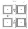
- a unit 130 according to a further embodiment of the inventionincludes a structure consisting of a main unit substrate 102 and one or more interposers 104 and 106 . Each interposer overlies only a portion of the bottom surface of main substrate 102 , leaving a further portion of the bottom surface unoccupied. Microelectronic elements such as element 141 may be mounted on the unoccupied port of the bottom surface, on the aligned portion of the top surface or both.
- Interposers 104 and 106may be separate elements, or may be a ring-like structure having a central opening which is aligned with the unoccupied portion of the main substrate 102 .
- Interposer 106includes a dielectric substrate such as a single-layer or multi-layer circuit panel substrate. Interposer 106 has terminals 140 exposed at its bottom surface and terminals 141 exposed at its top surface. Here again the main substrate 102 has terminals 138 exposed at its top surface and terminals 139 exposed at its bottom surface. As discussed below, signal rerouting between column positions is handled by the interposer rather than by the electrical connections on the main substrate. Thus, it is not essential to make the main substrate as a “two metal” structure for purposes of accomplishing rerouting between column positions.
- main substrate 102may be a “single metal” structure so that a single metallic element defines both the terminals 138 exposed at the top surface and the terminals 139 exposed at the bottom surface of the main substrate through a hole 110 in the dielectric of the main substrate.
- Terminals 139 and 141 exposed at the confronting faces of the main substrate 102 and interposer and 106are referred to herein as “internal” terminals inasmuch as they make connections within the unit, rather than connections to another unit in the stack, whereas terminals 138 and 140 are referred to herein as “external” terminals and constitute the top terminals 138 of the unit and the bottom terminals 140 of the unit.
- the interposertypically is a two metal structure, the interposer occupies a smaller area than the main substrate. As the cost penalty associated with fabrication of a two metal structure is incurred only over a smaller area, the costs of fabricating the entire assembly are reduced. Also, as best seen in FIG. 12 , the solder balls 110 or other conductive elements used to connect the interposer with the main substrate 102 are stacked on top of the solder balls 112 used to connect the interposer with the next unit in the stack or with a printed circuit board. Moreover, the interposer 104 itself adds height.
- an adequate height h below the main interposer 102 to accommodate microelectronic element 141can be provided using relatively small solder balls. This, in turn, decreases the required horizontal spacing between solder balls at adjacent column positions and hence decreases the required size of the main substrate.
- the internal terminal 141is electrically connected to the external terminal 140 at the next column position in a set of column positions.
- Thisprovides a connection between the top external terminal 138 of the unit and the bottom external terminal 140 of the unit at the next column position.
- top external terminal 138 1 ( 1 ) on unit 130 - 1 at column position CP 1is electrically connected to bottom external terminal 140 2 ( 1 ) on the bottom surface of interposer 106 , which forms the bottom surface of unit 130 - 1 .
- That external terminalis connected through a similar arrangement in the next unit 130 - 2 so that at the bottom of unit 130 - 2 the connection runs to bottom external terminal 140 3 ( 2 ) at column position CP 3 .
- Units with this arrangementprovide a “stair step” routing within the stack, identical to the routing discussed above with reference to FIG. 10 .
- such a unitoptionally may have a connection between the top external terminal 138 at the highest-ordered column position of a set of column positions and the bottom external terminal 104 of the lowest-ordered column position.
- the top external terminal 138 of each unitis electrically connected to the internal terminal 141 on the interposer, such a connection optionally can be made by conductive elements of the interposer, such traces 187 and vias 189 which electrically connect the internal terminal 141 at the highest-ordered column position of the set (CP 3 in FIG. 13 ) and the bottom external terminal 140 of at the lowest-ordered column position of the set.
- Stair step routing within unitscan be used, for example in forming stacks of memory chips.
- a typical memory chip package of a type used without stair step routingis depicted in FIG. 14 .
- the chiphas 4 contacts, commonly referred to as DQ connections 101 and also has one or more clock connections 103 .
- DQ connections of the first four chipssupply 4 ⁇ 4 or 16 separate connections for the 16 bits, whereas the fifth chip supplies four check bits. Each separate bit must be routed to a separate pad on a circuit panel.
- To make a 32-bit memory stackten such chips are stacked on one another.
- Two sets of five chipsshare a single set of five pads on the circuit panel, but are actuated with separate clock signals, achieved by bringing the clock pad 103 of five chips to one pad on the circuit panel and routing the same clock pad on another set of five chips to a different pad.
- the first tapereferred to as a “A” tape
- the first tapehas a first set of four pairs of traces. Each pair includes a trace 105 A running to the left, and a trace 105 B running to the right. Only one such pair, associated with DQ contact 101 a , is depicted in FIG. 14 for clarity of illustration; the other pairs are similar. Each trace extends to a separate column position.
- the 4 DQ contactscan be connected to a set of four terminals at four column positions on the left side of the package.
- DQ contacts 101 Acan be bonded to trace 105 B, and the other DQ contacts can be bonded to the other, similar traces (not shown) running to the right side of the package, so as to connect the four DQ contacts to terminals at a different set of four column positions along the right side of the package.
- Another tapereferred to as the B tape
- the B tapeis made with a different set of, such as traces 107 A and 107 B associated with contact 101 A.
- traces 107 A and 107 Bassociated with contact 101 A.
- four pairs of tracesare provided, one for each DQ contact; each pair again includes a trace running to a column position on the left and a trace running to a column position on the right. These traces, however, extend to different column positions than the corresponding traces of the A tape.
- the B tapecan be connected with a left or right bond-out, so as to connect the four DQ contacts to terminals at either of two sets of column positions.
- a third tapereferred to as the C tape
- traces 109 and similar traces for the other DQ contactsare made with traces 109 and similar traces for the other DQ contacts, so that the DQ contacts can be routed to terminals at a fifth set of column positions, different from the column positions provided by the A and B tapes.
- All of these tapeshave a set of two clock traces 111 A and 111 B allowing the routing of clock pad 103 to either of two column positions associated with either of two pads on the circuit board carrying the two different clock signals.
- the stacked packageis made by assembling the various tapes with the various bond-outs in a stack, with direct or “normal” connections between terminals at the same column positions in all of the tapes, so that all of the terminals at any given column position are connected in a vertical conductive path.
- the tapeis provided with traces which connect each of the DQ pads 101 to a single terminal, at a single column position associated with that DQ pad.
- the interposerprovides stair step routing at this column position, so that signals associated with this terminal on each of the five packages in the stack are routed to five different pads on the circuit board.
- a ten high stack(32 bit memory) can be made using the same approach, but with the clock contact 103 routed to either of two column positions using left or right bonding of clock traces as discussed above with reference to FIG. 14 .
- the clock contact on the chipcan be routed to a single column position on all of the units, and the interposer can provide conductive paths which repeatedly cross one another as discussed below with reference to FIG. 16 so that the terminal at this column position is connected in a first conductive path carrying clock 0 at some units and in a second conductive path carrying clock 1 at other units.
- the interposercan provide conductive paths which repeatedly cross one another as discussed below with reference to FIG. 16 so that the terminal at this column position is connected in a first conductive path carrying clock 0 at some units and in a second conductive path carrying clock 1 at other units. In this arrangement, only one bond-out is required for the entire assembly of a 32-bit memory.
- a unit 230includes a main substrate 202 and an interposer 206 similar to those discussed above.
- interposer 206provides crossover routing similar to that discussed above with reference to FIGS. 7 and 8 .
- internal terminal 241 - 1 at a first column positionis electrically connected through traces and vias to external terminal 240 - 2 at a second column position, whereas internal terminal 241 - 2 at the second column position is electrically connected to internal terminal 240 - 1 at the first column position.
- unit 230as a whole provides a crossover routing so that top external terminal 238 - 1 at the first column position is connected to bottom external terminal 240 - 2 at the second column position, whereas top external terminal 238 - 2 at the second column position is connected to bottom external terminal 240 - 1 at the first column position.
- a unit according to this embodimentcan be used in the assemblies discussed above with reference to FIGS. 1 through 11 .
- units made using an interposer with crossover routingcan be used to minimize the number of separate tapes required for making a memory stack as discussed above.
- the main substratemay be a tape with the same configuration as the A tape discussed above with reference to FIG. 14 .
- the interposeris configured to reroute the signals from each column position CP-A associated with tape A to the corresponding column position CP-B associated with tape B, and vice-versa. However, there are no connections to the chip at the B column positions.
- the stacked unitsthus define crossing conductive paths 201 and 203 ( FIG. 16 ).
- Unit 230 - 1has one of its DQ contacts connected to path 203
- the next unit 230 - 2has the same DQ contacts connected to conductive path 201 .
- Unit 230 - 3has the same DQ contact connected to path 203
- unit 230 - 4has the same DQ contact connected to path 201 .
- two DQ contactsare connected to each of these two conductive paths.
- the clocks in units 230 - 1 and 230 - 2are connected to clock signal 1
- units 230 - 3 and unit 230 - 4are connected to clock signal 0 .
- four distinct bitsare supplied through each of two paths 201 and 203 to circuit board 205 .
- Two bitsare supplied at each of the two clock signals.
- Tape Cis still used to supply the check bits.
- crossing conductive paths of this typecan be used to carry route two different clock signals to alternate units of a stack.
- the same interposercan be made with stair-step routing at some column positions and with crossover routing at other column positions.
- a unit according to a further embodiment of the inventionincludes a structure such as a dielectric substrate 330 having an elongated, strip-like central region 302 and one or more rows of terminals, including top terminals 338 and bottom terminals 340 ( FIG. 18 ) extending within the central region 302 of the substrate.
- the substratealso includes a pair of edge regions 304 and additional top terminals 339 and bottom terminals 340 disposed in these edge regions.
- Two microelectronic elements 308are mounted to structure 330 . Each microelectronic element has a contact-bearing surface 310 and contacts 312 exposed at such surface.
- the contactsinclude common contacts 312 A and 312 B ( FIG. 17 ).
- the contactsalso include unique contacts 312 C which may be disposed anywhere on the front surface.
- the microelectronic elementsare mounted to the structure 330 on opposite sides of central region 302 and disposed so that the first edges 314 of both microelectronic elements lie adjacent the central region.
- the same common contacts on both microelectronic elementsare disposed adjacent the same end of the central region. For example, common contacts 312 A on both elements 308 lie near one end of the central region 302 (close to the top of the drawing in FIG. 17 , whereas common contacts 312 B lie adjacent the opposite end of the central region, close to the bottom of the drawing in FIG. 17 ).
- the microelectronic elements 308are identical to one another.
- the desired placement of the contactscan be achieved by mounting one microelectronic element 308 A to the top surface of structure 330 and the other microelectronic element 308 B to the bottom surface of the structure.
- This arrangementprovides a short, simple routing from the common contacts 312 A, 312 B to the terminals 338 , 340 in the central region.
- units of this typecan be stacked.
- the microelectronic elements and the top surfaces of the various structures 330 aligned with one another and with the microelectronic element 308 B on the bottom surfaces of the structurealso aligned with one another. This arrangement does not materially increase the stack height.
- microelectronic element 308 Bis made with a substantially identical function to element 308 A but with contacts 312 disposed in a mirror image of the contact pattern on microelectronic element 308 A.
- both microelectronic elementsmay be mounted on the top surface and still provide the desired contact arrangement as seen in FIG. 17 .
- the unitmay include four microelectronic elements. Two identical units are mounted above and below the structure 330 on opposite sides of central region 302 in the manner illustrated in FIGS. 17 and 18 , whereas two other microelectronic elements with a mirror image contact pattern are mounted above and below the structure, so that the second (mirror image) elements lie directly above and directly below the first elements.
- conductive elementscan be used to interconnect the terminals of the units with one another.
- dielectric elements with pinsare shown in U.S. Provisional Patent Applications 60/533,210;60/533,393 and 60/533,437, all filed Dec. 30, 2003, the disclosures of which are incorporated by reference herein.
- the use of such pins as connecting elements in a stacked packageis described in U.S. Provisional Patent Application 60/583,066, filed Jun. 25, 2004, and in the provisional patent application entitled Stacked Packages With Pin Conductors and Chip Select Elements, filed on or about Oct. 25, 2004, the disclosures of which are also incorporated by reference herein.
- Other forms of stacked packages using other types of pinsare disclosed in PCT Published International Application WO2004/077525, the disclosure of which is also incorporated by reference herein.
- top”, bottom”, “up”, “down” and the likerefer to the frame of reference of the structure itself, and need not correspond to the normal gravitational frame of reference.
- terminals and other conductive featuresare described herein as being “exposed at” certain surfaces of dielectric elements.
- a conductive featureis “exposed at” a surface of a dielectric element if the conductive feature is accessible for contact with a point moving toward such surface from outside the dielectric element.
- a conductive feature exposed at a surface of a dielectric elementmay project from such surface; may be flush with such surface; or may be recessed below such surface in a hole or depression in such surface.
- the vertical directions of the various componentsare shown as perpendicular to the horizontal directions. This is the most commonly used arrangement.
- a stackmay have a sloping vertical direction, oblique to the horizontal planes of the unit substrates as, for example, where the conductive elements connecting terminals on adjacent unit substrate are canted.
- the vertical directionmay change slope at one or more places along the vertical extent of the stack, so that a “vertical” line zigags, as where alternate layers of conductive elements are canted in opposite directions. Any of these arrangements can be used.
Landscapes
- Engineering & Computer Science (AREA)
- Microelectronics & Electronic Packaging (AREA)
- Power Engineering (AREA)
- Computer Hardware Design (AREA)
- Physics & Mathematics (AREA)
- Condensed Matter Physics & Semiconductors (AREA)
- General Physics & Mathematics (AREA)
- Structures For Mounting Electric Components On Printed Circuit Boards (AREA)
- Semiconductor Integrated Circuits (AREA)
Abstract
Description
- This application claims the benefit of the filing date of U.S. Provisional Patent Application No. 60/517,179, filed Nov. 4, 2003, the disclosure of which is hereby incorporated by reference herein.
- The present invention relates to microelectronic packaging and systems.
- Microelectronic elements such as semiconductor chips are commonly provided in packages having terminals connected to the microelectronic element itself, such terminals being available for connection to external elements such as printed circuit boards.
- Some microelectronic elements, notably memory chips, have been provided heretofore in stacked arrangements with packages superposed one atop the other to conserve space on a circuit board. Such structures typically involve only a few chips and relatively simple connections which normally do not involve interconnections between chips in the stack, or between multiple stacks of chips. Even in these situations, it is sometimes necessary to provide different packages for different chips in the stack.
- One aspect of the present invention provides a stacked packaging arrangement especially useful for, e.g., logic chips such as field programmable gate arrays (hereinafter “FPGA”) or microprocessors, in which the stacked packaging arrangement accommodates logical interconnections between chips where inputs from one chip are connected to outputs of other chips. A further aspect of the invention provides designs for individual units and elements which can be used in such stacked arrangement. Yet another aspect of the invention provides a system-level design which allows for integration of multiple stacked packages while minimizing the complexity of signal routing in a printed circuit board (“PCB”) or other circuit panel used in the system. Still other aspects of the invention provide unit configurations which facilitate routing of signals to chips on different packages in a stack.
FIG. 1 is a diagrammatic top plan view of a unit in accordance with one embodiment of the invention.FIG. 2 is a diagrammatic bottom plan view of the unit shown inFIG. 1 .FIG. 3 is a fragmentary, diagrammatic elevational view showing a portion of an assembly including the unit ofFIGS. 1 and 2 .FIG. 4 is a diagrammatic perspective view of the assembly depicted inFIG. 3 .FIG. 5 is a fragmentary, diagrammatic, sectional view taken along line5-5 inFIG. 4 .FIG. 6 is a diagrammatic top elevational view of a component used in the assembly ofFIGS. 3-5 .FIG. 7 is a fragmentary, partially schematic sectional view showing a portion of the unit depicted inFIG. 1 .FIG. 8 is a fragmentary, diagrammatic elevational view showing a portion of the assembly depicted inFIGS. 3-5 , with certain components omitted for clarity of illustration.FIG. 9 is a view similar toFIG. 8 , but depicting a further portion of the assembly.FIG. 10 is a view similar toFIGS. 8 and 9 , but depicting yet a further portion of the assembly.FIG. 11 is a further fragmentary, diagrammatic elevational view depicting yet another portion of the same assembly.FIG. 12 is a diagrammatic sectional view depicting a unit in accordance with a further embodiment of the invention.FIG. 13 is a fragmentary, diagrammatic sectional view depicting a portion of an assembly including units as shown inFIG. 12 .FIG. 14 is a diagrammatic top plan view of a portion of a memory assembly.FIG. 15 is a fragmentary, diagrammatic sectional view depicting a portion of a unit in accordance with a further embodiment of the invention.FIG. 16 is a diagrammatic elevational view depicting an assembly incorporating a plurality of units as shown inFIG. 15 .FIG. 17 is a diagrammatic top plan view depicting a unit in accordance with yet another embodiment of the invention.FIG. 18 is a diagrammatic elevational view depicting an assembly incorporating units as shown inFIG. 17 .- A system according to one embodiment of the invention uses a plurality of units30 (
FIGS. 1 and 2 ). Each unit includes aunit substrate 32 in the form of a dielectric element such as a circuit board or flexible circuit panel, commonly referred to as a “tape.” The unit substrate defines a top side34 (FIG. 1 ) and a bottom side36 (FIG. 2 ). Each unit substrate hastop unit terminals 38 exposed at the top side of the unit andbottom unit terminals 40 exposed at its bottom side. - Each unit also includes a first microelectronic element in the form of a
semiconductor chip 41, in this case, an FPGA. In the particular design illustrated, each unit also includes additional semiconductor chips orSRAMs 43. The SRAM within each unit cooperates with the FPGA of that particular unit. In the embodiment illustrated, the FPGA chip is flip-chip mounted to the top of the unit substrate, so that the unit substrate serves as the package for the FPGA. The SRAMs are supplied in separate chip size packages, which are LGA-bonded to the bottom side of the unit substrate. Any other chip mounting techniques can be used. - One portion of a
unit substrate 32 is shown inFIG. 3 . In the particular embodiment illustrated,terminals FIG. 1 is referred to herein as the “north” direction (“N”); whereas an orthogonal horizontal direction, to the bottom of the drawing inFIG. 1 , is referred to herein as the “west” direction (“W”). Thetop terminals 38 and thebottom terminals 40 are disposed in positions referred to herein as column positions. Terminals at the same column position on a given unit are disposed at the same position in the horizontal directions of the unit. - Although the particular embodiment is described with reference to solderable units, it should be appreciated that units having other forms of terminals on their top and bottom sides can be employed. Merely by way of example, the terminals may be in the forms of pins and sockets, metallic bumps or other conductive contacts. Also, it is not necessary to employ a flat, board-like, or tape-like substrate such as the substrate depicted. For example, each unit substrate may be a ceramic or other chip carrier having a pocket or hole arranged to receive the chip or chips and having contacts on top and bottom sides of the substrate. Indeed, where a single semiconductor chip incorporates all of the functions required within a single unit, the chip itself can be provided with terminals on its top and bottom sides, so that each unit consists only of the chip. In a further variant, some or all of the terminals on the top and bottom sides of the substrate may be formed by common elements. For example, as disclosed in co-pending, commonly assigned U.S. patent application Ser. No. 10/267,450, filed Oct. 9, 2002, the disclosure of which is incorporated by reference herein, a terminal in the form of a pad disposed on one surface of the substrate may be exposed to the opposite surface of the substrate through a hole in the substrate, so that the same pad defines terminals exposed at both sides of the substrate. The SRAM chips incorporated within each unit cooperate with the FPGA of such unit. Each unit incorporates appropriate connections (not shown) between the SRAM and the FPGA.
- As best seen in
FIG. 4 , the units are arranged in four stacks (42-0,42-1,42-2 and42-3). Each stack includes four units superposed, one above the other. For example, stack42-0 includesunits circuit board 44. For clarity of illustration,circuit board 44 is shown as a transparent plane outlined by a solid black line inFIG. 4 . As best seen inFIG. 5 ,circuit panel 44 is a multilayer circuit board including several layers of dielectric material and internal conductors (not shown), as well as other conventional elements commonly found in a circuit board.Circuit board 44 has anupper surface 46 withupper pads 48 exposed at such upper surface, and has an oppositely directedlower surface 50 withlower pads 52 exposed atlower surface 50. As shown inFIGS. 4 and 5 , two units of each stack lie abovePCB 44, whereas two units lie below the PCB. For example, in stack42-0,units units Units PCB 44, have theirtop sides 34 facing upwardly, away from the PCB, whereasunits top sides - The units within each stack are aligned with one another in their horizontal directions, so that terminals on all of the units in the same column position are vertically superposed above one another. Stated another way, a vertical line drawn through a terminal at a particular column position on one unit will pass through all of the other terminals at the same column position on the other units in the stack.
- At numerous column positions, the terminals of all of the units within the stack are connected so that all of the terminals disposed at the same column position are connected to one another and connected to the printed circuit board. In this arrangement, referred to as a “normal stack connection” and shown in
FIG. 3 , the top terminal at each position on a given unit is electrically connected to the bottom terminal at the same position on the same unit. Moreover, the bottom terminal at each position is electrically connected by one or more conductive elements to the top terminal of the next lower unit at the same position. For example, as shown inFIG. 3 , top terminal38ais connected to thebottom terminal 40aof thesame unit 30a, and in turn, electrically connected to top terminal38bof the nextlower unit 30b. - As further discussed below, elements referred to herein as
interposers 60 and62 (shown as transparent planes with broken line borders inFIG. 4 , and also shown inFIGS. 3 and 5 ) extend between portions of the units in each stack. As also discussed below,interposer interposers terminals interposer 60 inFIG. 3 . These terminals simply form part of the conductive connection between thebottom terminal 40 on each unit and thetop terminal 38bon the next lower unit in the stack at the same column position. The conductive connections desirably include conductive bonding materials such as solder masses. As seen inFIG. 3 , asolder mass 68 connects lower terminal40ato thecorresponding terminals 64 on the top surface ofinterposer 60, whereas a further solder element such as a relativelythin solder layer 70 connectsterminal 66 of the interposer to thetop terminal 38bofsecond unit 30bin the stack. - At those column positions where a straight-through or normal connection runs throughout the entire stack, printed
circuit board 44 has a pair of upper andlower pads pads FIG. 3 ).Pads upper pad 48alies directly abovelower pad 52aat the same column position. These pads are electrically connected to one another by aconductor 72 extending through the printed circuit board. As depicted inFIG. 3 ,conductor 72 is a simple via extending straight through all of the layers (not shown) of the printed circuit board. This is not essential; the conductor connecting the pads of a common pair may include horizontal or zigzag portions, as required to route the connection around other conductors in the printed circuit board. However, a straight or nearly straight-through vertical conductor is preferred. The common pair of pads on the circuit board and the conductor connecting these pads forms part of a conductive connection at the column position between the units above the PCB and the units below the PCB. Thus, as seen inFIG. 3 , thebottom unit terminal 40bon thesecond unit 30bin the stack, immediately above the PCB, is connected to theupper pad 48aof the common pair by a further conductive element such as asolder ball 74; whereas thelower pad 52aof the common pair is connected by another conductive element such as asolder ball 76 to thetop unit terminal 38con thethird unit 30c, disposed immediately below the printed circuit board. This configuration is repeated at all column positions where a normal or a straight-through connection extending through the entire stack is desired. The ability to make connections between portions of the stack above and below the printed circuit board using a relatively simple, desirably straight connection through the board greatly simplifies the board layout. - As best seen in
FIG. 6 , theupper interconnect interposer 60 is a large circuit panel, such as a rigid or flexible circuit board. The interconnect interposer includes four holes78-0 through78-3 extending through the panel from its top surface to its bottom surface. The interconnect interposer further includes an array oftop interposer terminals 64 surrounding each hole on the top side of the interconnect interposer. Each such array of terminals includes terminals at the same column positions as the terminals of the individual units in one stack.Interposer 60 also has a corresponding array of bottom interposer terminals (66;FIG. 3 ) on its bottom surface.Upper interposer 60 desirably has conductive connections such astraces 80 extending between the various terminal arrays, and particularly, between the mutually adjacent edges of the various terminal arrays. These are shown only schematically inFIG. 6 . These traces are connected to selected ones of the top and bottom terminals to interconnect the stacks with one another, as further discussed below. Theupper interposer 60 intersects all four of the stacks, as does the lower interposer. Only a portion of the interconnect interposer or mezzanine interposer is seen inFIG. 5 . One array oftop interposer terminals 64 and the corresponding array of bottom interposer terminals66 (FIG. 3 ) surrounding hole78-0 is disposed in alignment with the unit terminals of the units in stack42-0, whereas hole78-0 is aligned with the chips of the units in stack42-0 so that the chips are received in the hole. - At those column positions where a normal stack connection, as discussed above with reference to
FIG. 3 is desired, the top andbottom interposer terminals FIG. 2 ) on the bottom of one unit and the FPGA41 (FIG. 1 ) on the top of the next lower unit. The use of small solder balls is advantageous, in that it allows the use of relatively small diameter terminals, which conserves space on the surfaces of the units. - The
upper interposer 60 is connected in each of the other stacks42-1 through42-3 in the same manner. The lower interposer (62;FIGS. 4 and 5 ) is configured similarly to the upper interposer, and also intercepts all four of the stacks in the same way as the upper interposer. Thelower interposer 62 performs exactly the same spacing function with respect to the units disposed below the PCB. - The various first microelectronic elements or
FPGAs 41 located within the stacks are interconnected with one another. At each such interconnection, an output of one FPGA is connected to an input of another FPGA. As mentioned above, the internal structure of every unit is identical to the individual structure of every other unit. For example, each unit has a top terminal at a given column position connected to an output or contact of the FPGA chip itself. Likewise, each unit has a top terminal at another position, connected to an input pad on the FPGA of the unit. Thus, connecting all of the terminals at the same column position within a particular stack to one another would not connect inputs to outputs, but instead would short inputs together and short outputs together. - To provide connections between inputs and outputs of the first microelectronic elements or FPGAs of adjacent units within a stack, the terminals associated with the input and output pads are arranged and connected as shown at
FIGS. 7 and 8 . Each unit has a set of terminals, referred to herein as “A” terminals. This set of terminals includes a top terminal38-A disposed at a first column position. Like all of the othertop terminals 38, this terminal (also referred to as a “top A terminal”) is exposed at thetop surface 34 ofunit substrate 32. The set of A terminals also includes one of thebottom unit terminals 40, referred to herein as a bottom A terminal40-A, exposed at thebottom surface 36 at a second column position. The top and bottom A terminals are electrically connected to one another, as by a via86-A and traces88-A. Similarly, each unit also includes a set of “B” terminals. This set includes a top B terminal38-B exposed at the second column position, and hence lying directly above the bottom terminal40-A. The set of B terminals also includes a bottom B terminal40-B exposed on the bottom surface of the unit substrate at the first column position, directly below the top A terminal38-A. These B terminals are interconnected to one another as by via86-B and associated traces88-B. For clarity of illustration, the traces shown are shown inFIG. 7 as arcuate lines. Although these lines are shown as projecting from the surfaces of theunit substrate 32, in normal practice, they are traces extending along the surface of the substrate or within the substrate. The first microelectronic element orFPGA 41 in each unit has an output or A pad electrically connected to the A terminals and an input or B pad electrically connected to the B terminals. In the particular embodiment illustrated, where the FPGA is disposed on the top surface of the unit substrate, the A and B terminals typically are connected to the A and B pads respectively by traces extending along the top surface of the substrate, but any other form of connection may be used. - Here again, top and bottom terminals on adjacent units in the stack disposed at the same column position are connected to one another by
conductive elements 90.Conductive elements 90 are depicted as simple solder ball interconnects inFIG. 8 . In actual practice, these conductive interconnects may include top and bottom terminals ofinterposers FIG. 8 for clarity of illustration. - The bottom A terminal40-A(1) of the top-most unit30-1 is connected to the top B terminal38-B(2)of the next lower unit30-2. Conversely, the bottom B terminal of the top-most unit30-1 is connected to the top A terminal38-A(2) of the next lower unit30-2. Thus, the A terminals of each unit are connected to the B terminals of the adjacent unit, so that the output or A pad of the FPGA41 (
FIG. 7 ) in each of these two units is connected to the input or B pad of the FPGA41 (FIG. 7 ) in the other one of these units. As also shown inFIG. 8 , the connections are carried down toupper pads 48 on the PCB. However, these connections are not necessary for interchange of information between the units. The conductive connections between the lower unit30-2 andpads 48 could be omitted, but preferably are used so as to avoid the need for special solder ball arrangements at different locations within the stack. Also, if desired, thePCB 44 can be provided with traces so that these signals can be accessed from outside the stack. At these column positions, the PCB does not connect through to the other units (30-3 and30-4) of the stack, below the PCB. These other units, however, are connected to one another in exactly the same way as units30-1 and30-2 are connected to one another. - The connection discussed with reference to
FIGS. 7 and 8 provides conductive paths which cross between column positions. Thus, one such conductive path extends at a first column position at terminal38-A(1) at the top of the stack and then at a second column position (at terminals40-A(1) and38-B(2) in the middle of the stack, and then crosses again back to the back to the first column position at terminal40-B(2) and the associatedupper pad 48 of the substrate. The other crossed conductive path starts at the second column position at terminal38-B(1), crosses to the first column position in the middle of the stack at terminals40-B(1) and38-A(2), and then crosses back again to the second column position at terminals40-A(2) and the associatedpad 48 on the printed circuit board. These conductive paths are shaded differently inFIG. 8 for clarity of illustration. Similar crossing conductive paths exist in the lower portion of the stack, below the printed circuit board. In this embodiment, the crossing pair of conductive paths is applied to allow connections from inputs to outputs on different units, even though both units have the identical structure. Other applications for crossing conductive paths are discussed below. In this regard, it should be noted that the crossing conductive paths depicted inFIGS. 7 and 8 extend along a pair of column positions which are adjacent to one another. However, any two column positions within the stack can be crossed with one another. The connection traces which are used to provide the crossing (such astraces FIG. 7 ) would be longer when the column positions used for a pair of crossing conductive paths are not adjacent to one another. Also, a stack may include any number of crossings. Thus, an individual pair of conductive paths may cross one another once or more than once along the vertical extent of the stack. - In other instances, it is necessary to make connections between the output connections of the FPGA in one unit in a stack and the input or B connections of the FPGA in another, non-adjacent unit in the same stack. The arrangements used for such connections are shown in
FIG. 9 . Here again, interposers60 and62 are omitted for clarity of illustration. Here again, each unit includes a set of A terminals and a set of B terminals at first and second column positions CP1 and CP2 in exactly the same arrangement as discussed above with reference toFIGS. 7 and 8 . Here again, the A terminals (e.g.,38-A(1) and40-A(1)) on each unit are electrically connected to one another but are not electrically connected to the B terminals (38-B(1) and40-B(1)). Each unit also includes a set of C terminals and a set of D terminals at third and fourth column positions. The C terminals and D terminals are configured in a manner similar to the A and B terminals. For example, the C terminals on unit30-1 include a top C terminal38-C(1) at third column position CP3 and a bottom C terminal40-C(1) at fourth column position CP4, the C terminals being electrically connected to one another. The D terminals on this unit include a top D terminal38-D(1) at fourth column position CP4 and a bottom D terminal40-D(1) at the third column position CP3. The D terminals are electrically connected to one another by other traces and vias. - In each unit, the A terminals are connected to an output pad of the first microelectronic element or FPGA. However, the B terminals are not connected to a pad of the FPGA. The C terminals are connected to an input pad of the FPGA carried by the unit, whereas the D terminals are not connected to a pad of the FPGA. Here again, the bottom terminals of each unit are connected to the top terminals of the next adjacent unit, except that the bottom terminals of second unit30-2 are connected to the
upper pads 48 ofPCB 44 disposed at the same column positions, whereas the top terminals of unit30-3, disposed immediately below thePCB 44, are connected to thelower pads 52 of the PCB at the same column positions. In this instance, theupper pad 48 at each column position of the first through fourth column position shown inFIG. 9 is connected to thelower pad 52 of the circuit board at another column position at these first through fourth positions. The upper pad48-U1 at the first column position CP1 is connected to the lower pad52-L3 at the third column position. The output connection is carried from the A terminals38-A(1) and40-A(1) of top unit30-1 down through terminals38-B(2) and40-B(2) to upper pad48-U1 at first column position CP1, (shaded inFIG. 9 ) and routed along the PCB down to the lower pad52-L3 at the third column position. The solder ball below this PCB pad connects to the top C terminal38-C(3) on unit30-3 immediately below the PCB, and hence connects to the input pad of the FPGA in that unit. Here again, because the units are identical, the connection continues down through the bottom C terminal40-C(3) at the fourth column position, but the solder ball below that bottom C terminal connects to a D terminal38-D(4)on the top of bottom unit30-4, and hence, does not connect to the FPGA of this unit. Also, the conductive path connects to a B terminal38-B(2) on the second unit30-2 but does not make a connection to the FPGA of that unit, because the B terminals are not connected. Thus, the output of the FPGA in top unit30-1 is connected only to the input of the FPGA in third unit30-3 in the same stack. - The PCB also has an upper pad48-U2 at the second column position CP2 connected to a lower pad52-L4 at the fourth column position CP4. The output of unit30-2 is connected through these upper and lower pads on the PCB and through the other units to terminal30-C(4) of unit30-4. Likewise, the PCB has a lower pad52-L(1) at the first column position CP1 connected to an upper pad48-U3 at the third column position CP3, and also has a lower pad52-L2 at the second column position CP2 connected to an upper pad48-U4 at the fourth column position CP4. The lower pad52-L1 at the first column position, in conjunction with the conductive paths defined by the units, connect the A terminals, and hence the FPGA output contact of unit30-3 to the C terminals, and hence the FPGA input, of unit30-1. The lower pad52-L2 at the second column position and upper pad48-U4 at the fourth column position serve to connect the A terminals, and hence the FPGA output contact of unit30-4 to the C terminals, and FPGA input contact of unit30-2.
- At still other locations within each stack, there are unique connections between the units of the stack and the printed circuit board. That is, a signal is routed from the PCB to only one unit in the stack. Where these unique connections are desired,
top terminals 38 andbottom terminals 40 are provided on each unit at a set of four column positions CP1 through CP4 as shown inFIG. 10 . Here again, these column positions are depicted as physically adjacent to one another for clarity of illustration, but need not be physically adjacent to one another. At each of these column positions, each unit has a bottom terminal and a top terminal. Within each unit, eachtop terminal 38 is connected to thebottom terminal 40 in the next-higher column position of the set. For example, the bottom terminal40-4(4) onunit 4 at the fourth column position CP4 is electrically connected to the top terminal38-3(4) of the same unit in the third column position. These connections can be made, for example, bytraces 88 andvias 86. Moreover, within each unit thetop terminal 38 at the highest-orderedcolumn position CP 4 of the set is electrically connected to thebottom terminal 40 at the lowest-ordered column position of the set, as byfurther traces 87 and via89. Here again, the traces are schematically indicated by lines shown extending above and below the planes of the unit substrates, but in practice these connections typically extend along the surfaces of the substrate or within the substrate. As seen inFIG. 10 , the electrical connections run in a stair-step fashion, traversing over one column position at each unit. Thus, the electrical connections traverse the shaded elements, including terminals40-4(4) and38-3(4) on unit30-4;40-3(3) and38-2(3) on unit30-3;40-2(2) and38-1(2) on unit30-2; and40-1(1) on unit30-1. Thus, each conductive path extends in a stair-step fashion, moving one column position towards the highest-ordered column position of the set (towards CP4) as it moves down one unit in the stack and, conversely, moving one column position toward the lowest-ordered column position (towards CP1) as it moves up one unit in the stack. Each unit has a connection between a particular contact (not shown) on a microelectronic element and thebottom terminal 40 at a particular column, position, in this case the first column position. For example, the first microelectronic element orFPGA 41 of unit30-1 has a contact connected to terminal40-1(1); the same contact on the first microelectronic element or FPGA of unit30-2 is connected to bottom terminal40-1(2) of unit30-2. Likewise, unit30-3 has the same contact on the microelectronic element connected to bottom terminal40-1(3), whereas unit30-4 at the bottom of the stack has the same contact pad of the microelectronic element connected to terminals40-1(4). The other top and bottom terminals at column positions CP1-CP4 are not connected to the microelectronic elements of the various units. The stair-step arrangement prevailing throughout these column positions brings the connections to the four different microelectronic elements to four different terminals40-1(4);40-2(4);40-3(4); and40-4(4) on the bottom of the bottom unit30-4. Acircuit board 44′ positioned at the bottom of the stack may have fourunique pads 48′-1 through48′-4 connected to these unique terminals. For example, a signal supplied from the PCB atpad 48′-4 in the fourth column position CP4 will pass to bottom terminal40-1(1) in the first column position of UNIT30-1. Similarly, the signal supplied through at the second column position throughpad 48′-2 (also shaded), will pass to the identical terminal40-1(3) on the bottom surface of unit30-3. - Moreover, each conductive path runs to the highest-ordered column position at top of the unit where the connection reaches the lowest-ordered column position. For example, the conductive path from terminal40-3(4), at the third column position on the bottom of unit30-4 runs up to bottom terminal40-1(2) at CP1 on unit30-2, and then to top terminal38-4(2) at CP4 on the same unit30-2. The conductive path thus connects to bottom terminal40-4(1) on the bottom of unit30-1 and thus to top terminal38-3(1) at CP3, on the top of the top unit30-1. Thus, each of the conductive paths extends through all four of the units, and ultimately returns to the same column position as it had at the bottom of the stack. Stated another way, the “stair-step” arrangement is topologically similar to a spiral staircase; in connection involving a set of N column positions, the arrangement repeats after N units. As further discussed below in connection with
FIG. 13 , units having such a spiral connection can be stacked more than N units high, so that some or all of the conductive paths connect to more than one unit. Also,FIG. 10 depicts four units disposed on the same side of the PCB. In the embodiment illustrated in the other figures, two units within each stack are disposed on the top and two units are disposed on the bottom, as indicated by thePCB 44 shown in broken lines inFIG. 10 . Because each conductive path passes through all of the units (at different column positions), the conductive paths will still connect to unique pads on acircuit board 44 at the location depicted in broken lines. Alternatively or additionally, pads on a top interposer shown in broken lines at60′ or abottom interposer 62′ can also be connected to unique conductive paths. The interposer or circuit board used in such an arrangement desirably has top and bottom pads directly connected to one another as discussed above in connection withFIG. 3 . Alternatively, only two column positions need be occupied by the stair-step set of column positions to provide unique connections to each of the units, provided that the PCB has separate pads on its top and bottom surfaces. Where the stack extends on each side of the PCB N units or less (N being the number of column positions in the set), the connection between the top pad at the highest-ordered column position and the bottom pad at the lowest-ordered column position (as defined bytraces 87 and via89 inFIG. 10 ) can be omitted. - The discussion above refers to connections with the first microelectronic element or FPGA in each of the various units. Any or all of these techniques can be used to provide connections with the second microelectronic elements in each of the various units.
- The foregoing discussion relates to connections within each individual stack. However, it is also necessary to connect units in different stacks to one another. In particular, inputs and outputs of FPGAs in units of different stacks must be connected to one another. Several features of the system facilitate these inter-stack interconnections. First, as seen in
FIG. 4 , the stacks are disposed in a grid, so that each stack has a side facing a side of another stack. For example, a side of stack42-0 faces a side of stack42-1, whereas another side of stack42-0 faces a side of stack42-3. However, two of the stacks are inverted relative to two of the other stacks. As seen inFIG. 1 , the bottom of stack42-1 points upwardly relative to the PCB (upwardly in the drawing), whereas the top of stack42-0 points upwardly relative to thePCB 44. Stack42-2 has its top facing upwardly, whereas stack42-3 has its bottom facing upwardly. Further, stack42-2 is rotated 180° relative to stack42-0 about a vertical axis, whereas stack42-3 is rotated 180° relative to stack42-1. The net effect is that corresponding sides of the stacks face one another. That is, the westerly side of stack42-0 faces the westerly side of stack42-1, whereas the northerly side of stack42-1 faces the northerly side of stack42-2, and so on. The terminals which require inter-stack connections are placed along the westerly and northerly sides of the stacks. Theupper interposer 60 is provided with connection lines80 (FIG. 6 ) interconnecting terminals associated with the various stacks. Very short interconnect lines can connect terminals associated with the northerly edge of stack42-3 and the northerly edge of stack42-0, and similar short connection lines will connect the westerly edge of stack42-0 with the westerly edge of stack42-1, and so on. - As seen in
FIG. 11 , the top interposer has a set of top terminals64-1 and64-2 associated with column positions CP1 and CP2 of stack42-0, for example, on the westerly edge of stack42-0, electrically connected by traces80-1 and80-2 to corresponding top terminals64-3 and64-4, at column positions CP3 and CP4 on the westerly edge ofstack 1. At these column positions, each unit has top andbottom terminals FIG. 3 . At column position CP1, eachunit 30 has itsterminals terminals column positions CP 4 are connected to an input pad of the FPGA. Thus, the output from the FPGA in unit30-1-0 in stack42-0 is connected to the input of the FPGA in unit30-1-1 in stack42-1, and other connections are made in similar fashion. Thetop interposer 60 has a similar set ofbottom terminals 66 and associated traces, which interconnect other units in the two stacks with one another in the same manner. Thebottom terminals 66 and associated traces used for this function are electrically isolated from thetop terminals 64 and associated traces80-1 and80-2. Stated another way, at these column positions, the mezzanine interposer does not provide an interconnection between the units in a single stack. Thebottom interposer 62 is arranged in a similar fashion. - By routing inter-stack interconnections through the interposers, which are separate from the
PCB 44, the PCB can be greatly simplified. Further, packaging each FPGA with its associated SRAMs also avoids the needs for traces on the PCB for interconnecting FPGAs with SRAMs. The PCB, thus, can have many fewer layers than would be required otherwise. - As one example, a conventional PCB with four FPGAs mounted directly on the PCB, and with SRAMs connected to the FPGAs through the printed circuit board itself, requires a printed circuit board with more than 25 layers. Such a circuit board is extraordinarily complex, and hence suffers significantly in cost and reliability. By contrast, the design as discussed above can accommodate 16 FPGAs and 32 SRAMs in the same circuit board area or less, using a PCB having fewer layers.
- The features discussed above can be varied. For example, where an interposer is present between units in a stack, the mezzanine interposer may be provided with A and B pads at first and second column positions, as discussed above with reference to
FIGS. 7 and 8 so as to interchange signals between column positions in the interconnect interposer. In this case, there is no need to interchange signals between column positions in the units themselves. Therefore, the top and bottom terminals of each unit at each column position may be directly connected to one another in the manner shown atFIG. 3 , or else may be formed as parts of the same metallic pad. This can be used, for example, where the unit substrate has only a single layer of metal. - Also, the individual features discussed above can be utilized separately. For example, an arrangement utilizing a stack with portions disposed above and below a printed circuit board or other circuit panel, also referred to as a “mirrored” stack, is advantageous in and of itself, even where only one stack is used. Inter alia, by reducing the stack height on each side of the printed circuit board, cooling of the individual dies is greatly facilitated. Moreover, this result is achieved without the use of special “mirror image” sets of chips. As seen in
FIG. 5 , theconductive elements 90 are mounted on the top surfaces of the various units disposed below the circuit board, whereas the conductive elements are mounted on the bottom surfaces of the units disposed below the circuit board. The same arrangement can be used with any stackable units having terminals on its top and bottom surfaces, with or without the other features discussed above. - Also, chips other than FPGAs may be utilized. The number of chips per unit, the number of units per stack, and the number of stacks all can be increased or decreased.
- In the stacked packages discussed above, each unit has been described as having top and bottom terminals on the top and bottom surfaces of a single unit substrate. However, this is not essential. A
unit 130 according to a further embodiment of the invention (FIG. 12 ) includes a structure consisting of amain unit substrate 102 and one ormore interposers main substrate 102, leaving a further portion of the bottom surface unoccupied. Microelectronic elements such aselement 141 may be mounted on the unoccupied port of the bottom surface, on the aligned portion of the top surface or both.Interposers main substrate 102.Interposer 106 includes a dielectric substrate such as a single-layer or multi-layer circuit panel substrate.Interposer 106 hasterminals 140 exposed at its bottom surface andterminals 141 exposed at its top surface. Here again themain substrate 102 has terminals138 exposed at its top surface andterminals 139 exposed at its bottom surface. As discussed below, signal rerouting between column positions is handled by the interposer rather than by the electrical connections on the main substrate. Thus, it is not essential to make the main substrate as a “two metal” structure for purposes of accomplishing rerouting between column positions. As depicted inFIG. 13 ,main substrate 102 may be a “single metal” structure so that a single metallic element defines both the terminals138 exposed at the top surface and theterminals 139 exposed at the bottom surface of the main substrate through ahole 110 in the dielectric of the main substrate.Terminals main substrate 102 and interposer and106 are referred to herein as “internal” terminals inasmuch as they make connections within the unit, rather than connections to another unit in the stack, whereasterminals 138 and140 are referred to herein as “external” terminals and constitute the top terminals138 of the unit and thebottom terminals 140 of the unit. - The ability to use a single metal structure in the main substrate is a significant advantage. Although the interposer typically is a two metal structure, the interposer occupies a smaller area than the main substrate. As the cost penalty associated with fabrication of a two metal structure is incurred only over a smaller area, the costs of fabricating the entire assembly are reduced. Also, as best seen in
FIG. 12 , thesolder balls 110 or other conductive elements used to connect the interposer with themain substrate 102 are stacked on top of thesolder balls 112 used to connect the interposer with the next unit in the stack or with a printed circuit board. Moreover, theinterposer 104 itself adds height. Therefore, an adequate height h below themain interposer 102 to accommodatemicroelectronic element 141 can be provided using relatively small solder balls. This, in turn, decreases the required horizontal spacing between solder balls at adjacent column positions and hence decreases the required size of the main substrate. - In the embodiment illustrated in
FIG. 13 , at the particular column positions illustrated, theinternal terminal 141 is electrically connected to theexternal terminal 140 at the next column position in a set of column positions. This provides a connection between the top external terminal138 of the unit and the bottomexternal terminal 140 of the unit at the next column position. For example, top external terminal1381(1) on unit130-1 atcolumn position CP 1 is electrically connected to bottomexternal terminal 1402(1) on the bottom surface ofinterposer 106, which forms the bottom surface of unit130-1. That external terminal is connected through a similar arrangement in the next unit130-2 so that at the bottom of unit130-2 the connection runs to bottomexternal terminal 1403(2) atcolumn position CP 3. Units with this arrangement provide a “stair step” routing within the stack, identical to the routing discussed above with reference toFIG. 10 . As discussed above in connection withFIG. 10 , such a unit optionally may have a connection between the top external terminal138 at the highest-ordered column position of a set of column positions and the bottomexternal terminal 104 of the lowest-ordered column position. Because the top external terminal138 of each unit is electrically connected to theinternal terminal 141 on the interposer, such a connection optionally can be made by conductive elements of the interposer,such traces 187 and vias189 which electrically connect theinternal terminal 141 at the highest-ordered column position of the set (CP3 inFIG. 13 ) and the bottomexternal terminal 140 of at the lowest-ordered column position of the set. - Stair step routing within units can be used, for example in forming stacks of memory chips. A typical memory chip package of a type used without stair step routing is depicted in
FIG. 14 . Inter alia, the chip has 4 contacts, commonly referred to asDQ connections 101 and also has one ormore clock connections 103. To make a 16 bit memory stack, five such chips are stacked on one another. DQ connections of the first four chips supply 4×4 or 16 separate connections for the 16 bits, whereas the fifth chip supplies four check bits. Each separate bit must be routed to a separate pad on a circuit panel. To make a 32-bit memory stack, ten such chips are stacked on one another. Two sets of five chips share a single set of five pads on the circuit panel, but are actuated with separate clock signals, achieved by bringing theclock pad 103 of five chips to one pad on the circuit panel and routing the same clock pad on another set of five chips to a different pad. Such a system can be made using three different packages or “tapes”. The first tape, referred to as a “A” tape, has a first set of four pairs of traces. Each pair includes a trace105A running to the left, and a trace105B running to the right. Only one such pair, associated withDQ contact 101a, is depicted inFIG. 14 for clarity of illustration; the other pairs are similar. Each trace extends to a separate column position. By bonding pad101A to trace105A and the bonding the other DQ contacts to the other similar traces (not shown) running to the left side of the package (referred to as a “left bond-out”), the 4 DQ contacts can be connected to a set of four terminals at four column positions on the left side of the package. Alternatively, using the same tape, DQ contacts101A can be bonded to trace105B, and the other DQ contacts can be bonded to the other, similar traces (not shown) running to the right side of the package, so as to connect the four DQ contacts to terminals at a different set of four column positions along the right side of the package. Another tape, referred to as the B tape, is made with a different set of, such as traces107A and107B associated with contact101A. Here again, four pairs of traces are provided, one for each DQ contact; each pair again includes a trace running to a column position on the left and a trace running to a column position on the right. These traces, however, extend to different column positions than the corresponding traces of the A tape. As with the A tape, the B tape can be connected with a left or right bond-out, so as to connect the four DQ contacts to terminals at either of two sets of column positions. Finally, a third tape, referred to as the C tape, is made withtraces 109 and similar traces for the other DQ contacts, so that the DQ contacts can be routed to terminals at a fifth set of column positions, different from the column positions provided by the A and B tapes. All of these tapes have a set of two clock traces111A and111B allowing the routing ofclock pad 103 to either of two column positions associated with either of two pads on the circuit board carrying the two different clock signals. The stacked package is made by assembling the various tapes with the various bond-outs in a stack, with direct or “normal” connections between terminals at the same column positions in all of the tapes, so that all of the terminals at any given column position are connected in a vertical conductive path. A This requires the circuit assembler to handle and stock three different tapes and a total of five different bond outs, i.e. tape A left bonding, tape A right bonding, tape B left bonding, tape B right bonding, tape C and all withclock contact 103 bonded to the appropriate trace111A forclock 0 in order to make a 16-bit memory (5 units stacked). Making a 32-bit memory (10 units stacked) requires the same 3 tapes in and, and an additional set of five bond outs withclock pad 103 bonded to the clock trace111B forclock 1. This poses significant logistical difficulties. - By contrast, using the approach shown in
FIGS. 12 and 13 , only a single tape and only a single bond out is required is required to make a five high stack (16 bit memory). The tape is provided with traces which connect each of theDQ pads 101 to a single terminal, at a single column position associated with that DQ pad. The interposer provides stair step routing at this column position, so that signals associated with this terminal on each of the five packages in the stack are routed to five different pads on the circuit board. A ten high stack (32 bit memory) can be made using the same approach, but with theclock contact 103 routed to either of two column positions using left or right bonding of clock traces as discussed above with reference toFIG. 14 . In a further alternative, the clock contact on the chip can be routed to a single column position on all of the units, and the interposer can provide conductive paths which repeatedly cross one another as discussed below with reference toFIG. 16 so that the terminal at this column position is connected in a first conductivepath carrying clock 0 at some units and in a second conductivepath carrying clock 1 at other units. In this arrangement, only one bond-out is required for the entire assembly of a 32-bit memory. - A
unit 230 according to a further embodiment of the invention includes amain substrate 202 and aninterposer 206 similar to those discussed above. However,interposer 206 provides crossover routing similar to that discussed above with reference toFIGS. 7 and 8 . Thus internal terminal241-1 at a first column position is electrically connected through traces and vias to external terminal240-2 at a second column position, whereas internal terminal241-2 at the second column position is electrically connected to internal terminal240-1 at the first column position. Thus,unit 230 as a whole provides a crossover routing so that top external terminal238-1 at the first column position is connected to bottom external terminal240-2 at the second column position, whereas top external terminal238-2 at the second column position is connected to bottom external terminal240-1 at the first column position. A unit according to this embodiment can be used in the assemblies discussed above with reference toFIGS. 1 through 11 . - Alternatively, units made using an interposer with crossover routing can be used to minimize the number of separate tapes required for making a memory stack as discussed above. In this arrangement, the main substrate may be a tape with the same configuration as the A tape discussed above with reference to
FIG. 14 . The interposer is configured to reroute the signals from each column position CP-A associated with tape A to the corresponding column position CP-B associated with tape B, and vice-versa. However, there are no connections to the chip at the B column positions. The stacked units thus define crossingconductive paths 201 and203 (FIG. 16 ). Unit230-1 has one of its DQ contacts connected topath 203, whereas the next unit230-2 has the same DQ contacts connected toconductive path 201. Unit230-3 has the same DQ contact connected topath 203, whereas unit230-4 has the same DQ contact connected topath 201. Thus, two DQ contacts are connected to each of these two conductive paths. The clocks in units230-1 and230-2 are connected toclock signal 1, whereas units230-3 and unit230-4 are connected toclock signal 0. Thus, four distinct bits are supplied through each of twopaths circuit board 205. Two bits are supplied at each of the two clock signals. Tape C is still used to supply the check bits. As discussed above in connection withFIG. 13 , crossing conductive paths of this type can be used to carry route two different clock signals to alternate units of a stack. This can be done by connecting a 0 clock connected topath 201 and a 1 clock topath 203 atcircuit board 205, and by connecting the clock contact of the chip at each unit to the terminal at CP A inFIG. 16 . To provide such crossing routing in conjunction with the stair-step routing for the DQ signals discussed with reference toFIG. 13 , the same interposer can be made with stair-step routing at some column positions and with crossover routing at other column positions. - A unit according to a further embodiment of the invention (
FIG. 17 ) includes a structure such as adielectric substrate 330 having an elongated, strip-likecentral region 302 and one or more rows of terminals, includingtop terminals 338 and bottom terminals340 (FIG. 18 ) extending within thecentral region 302 of the substrate. The substrate also includes a pair ofedge regions 304 and additionaltop terminals 339 andbottom terminals 340 disposed in these edge regions. Two microelectronic elements308 are mounted to structure330. Each microelectronic element has a contact-bearingsurface 310 andcontacts 312 exposed at such surface. The contacts include common contacts312A and312B (FIG. 17 ). These are disposed adjacent afirst edge 314 of the front surface and hence adjacent the first edge of the microelectronic element. The contacts also include unique contacts312C which may be disposed anywhere on the front surface. The microelectronic elements are mounted to thestructure 330 on opposite sides ofcentral region 302 and disposed so that thefirst edges 314 of both microelectronic elements lie adjacent the central region. Also, the same common contacts on both microelectronic elements are disposed adjacent the same end of the central region. For example, common contacts312A on both elements308 lie near one end of the central region302 (close to the top of the drawing inFIG. 17 , whereas common contacts312B lie adjacent the opposite end of the central region, close to the bottom of the drawing inFIG. 17 ). In the embodiment shown inFIG. 17 and18, the microelectronic elements308 are identical to one another. Thus, the desired placement of the contacts can be achieved by mounting one microelectronic element308A to the top surface ofstructure 330 and the other microelectronic element308B to the bottom surface of the structure. This arrangement provides a short, simple routing from the common contacts312A,312B to theterminals FIG. 18 , units of this type can be stacked. The microelectronic elements and the top surfaces of thevarious structures 330 aligned with one another and with the microelectronic element308B on the bottom surfaces of the structure also aligned with one another. This arrangement does not materially increase the stack height. - In a further embodiment, microelectronic element308B is made with a substantially identical function to element308A but with
contacts 312 disposed in a mirror image of the contact pattern on microelectronic element308A. In this case, both microelectronic elements may be mounted on the top surface and still provide the desired contact arrangement as seen inFIG. 17 . In yet another arrangement, the unit may include four microelectronic elements. Two identical units are mounted above and below thestructure 330 on opposite sides ofcentral region 302 in the manner illustrated inFIGS. 17 and 18 , whereas two other microelectronic elements with a mirror image contact pattern are mounted above and below the structure, so that the second (mirror image) elements lie directly above and directly below the first elements. - As mentioned above, various types of conductive elements can be used to interconnect the terminals of the units with one another. For example, dielectric elements with pins are shown in U.S.
Provisional Patent Applications 60/533,210;60/533,393 and 60/533,437, all filed Dec. 30, 2003, the disclosures of which are incorporated by reference herein. The use of such pins as connecting elements in a stacked package is described in U.S.Provisional Patent Application 60/583,066, filed Jun. 25, 2004, and in the provisional patent application entitled Stacked Packages With Pin Conductors and Chip Select Elements, filed on or about Oct. 25, 2004, the disclosures of which are also incorporated by reference herein. Other forms of stacked packages using other types of pins are disclosed in PCT Published International Application WO2004/077525, the disclosure of which is also incorporated by reference herein. - Also, other features useful in stacked packages are disclosed in U.S. Published patent application Ser. Nos. 20030107118 and 20040031972, the disclosures of which are also incorporated by reference herein. For example, these published applications describe features which can be incorporated into the units of a stacked package to allow selective making or breaking of traces in the individual units, to provide still further routing versatility. These features can be used in conjunction with the features discussed above.
- Also, it should be appreciated that terms such as “top”, “bottom”, “up”, “down” and the like as used in this disclosure refer to the frame of reference of the structure itself, and need not correspond to the normal gravitational frame of reference. Further, terminals and other conductive features are described herein as being “exposed at” certain surfaces of dielectric elements. As used in this disclosure, a conductive feature is “exposed at” a surface of a dielectric element if the conductive feature is accessible for contact with a point moving toward such surface from outside the dielectric element. Thus, a conductive feature exposed at a surface of a dielectric element may project from such surface; may be flush with such surface; or may be recessed below such surface in a hole or depression in such surface.
- In the drawings, the vertical directions of the various components are shown as perpendicular to the horizontal directions. This is the most commonly used arrangement. However, a stack may have a sloping vertical direction, oblique to the horizontal planes of the unit substrates as, for example, where the conductive elements connecting terminals on adjacent unit substrate are canted. Also, the vertical direction may change slope at one or more places along the vertical extent of the stack, so that a “vertical” line zigags, as where alternate layers of conductive elements are canted in opposite directions. Any of these arrangements can be used.
- As these and other objects, features and advantages of the present invention can be utilized without departing from the present invention, the foregoing description of the preferred embodiments should be taken by way of illustration rather than by way of limitation of the present invention.
Claims (50)
Priority Applications (4)
| Application Number | Priority Date | Filing Date | Title |
|---|---|---|---|
| US10/981,067US7183643B2 (en) | 2003-11-04 | 2004-11-04 | Stacked packages and systems incorporating the same |
| US11/710,752US7589409B2 (en) | 2003-11-04 | 2007-02-26 | Stacked packages and microelectronic assemblies incorporating the same |
| US12/551,807US8704351B2 (en) | 2003-11-04 | 2009-09-01 | Stacked microelectronic assemblies |
| US14/257,795US9437582B2 (en) | 2003-11-04 | 2014-04-21 | Stacked microelectronic assemblies |
Applications Claiming Priority (2)
| Application Number | Priority Date | Filing Date | Title |
|---|---|---|---|
| US51717903P | 2003-11-04 | 2003-11-04 | |
| US10/981,067US7183643B2 (en) | 2003-11-04 | 2004-11-04 | Stacked packages and systems incorporating the same |
Related Child Applications (1)
| Application Number | Title | Priority Date | Filing Date |
|---|---|---|---|
| US11/710,752ContinuationUS7589409B2 (en) | 2003-11-04 | 2007-02-26 | Stacked packages and microelectronic assemblies incorporating the same |
Publications (2)
| Publication Number | Publication Date |
|---|---|
| US20050194672A1true US20050194672A1 (en) | 2005-09-08 |
| US7183643B2 US7183643B2 (en) | 2007-02-27 |
Family
ID=34915491
Family Applications (4)
| Application Number | Title | Priority Date | Filing Date |
|---|---|---|---|
| US10/981,067Expired - LifetimeUS7183643B2 (en) | 2003-11-04 | 2004-11-04 | Stacked packages and systems incorporating the same |
| US11/710,752Expired - LifetimeUS7589409B2 (en) | 2003-11-04 | 2007-02-26 | Stacked packages and microelectronic assemblies incorporating the same |
| US12/551,807Expired - LifetimeUS8704351B2 (en) | 2003-11-04 | 2009-09-01 | Stacked microelectronic assemblies |
| US14/257,795Expired - LifetimeUS9437582B2 (en) | 2003-11-04 | 2014-04-21 | Stacked microelectronic assemblies |
Family Applications After (3)
| Application Number | Title | Priority Date | Filing Date |
|---|---|---|---|
| US11/710,752Expired - LifetimeUS7589409B2 (en) | 2003-11-04 | 2007-02-26 | Stacked packages and microelectronic assemblies incorporating the same |
| US12/551,807Expired - LifetimeUS8704351B2 (en) | 2003-11-04 | 2009-09-01 | Stacked microelectronic assemblies |
| US14/257,795Expired - LifetimeUS9437582B2 (en) | 2003-11-04 | 2014-04-21 | Stacked microelectronic assemblies |
Country Status (1)
| Country | Link |
|---|---|
| US (4) | US7183643B2 (en) |
Cited By (34)
| Publication number | Priority date | Publication date | Assignee | Title |
|---|---|---|---|---|
| US20080185736A1 (en)* | 1999-02-08 | 2008-08-07 | Megica Corporation | Multiple selectable function integrated circuit module |
| US20090057900A1 (en)* | 2005-05-03 | 2009-03-05 | Megica Corporation | Stacked Chip Package With Redistribution Lines |
| JP2011061206A (en)* | 2009-09-11 | 2011-03-24 | E-Pin Optical Industry Co Ltd | Stacked disk optical lens array, stacked disk lens module array, and manufacturing method thereof |
| US8021976B2 (en) | 2002-10-15 | 2011-09-20 | Megica Corporation | Method of wire bonding over active area of a semiconductor circuit |
| US8148806B2 (en) | 2000-05-19 | 2012-04-03 | Megica Corporation | Multiple chips bonded to packaging structure with low noise and multiple selectable functions |
| US8168527B2 (en) | 2006-09-06 | 2012-05-01 | Megica Corporation | Semiconductor chip and method for fabricating the same |
| US8294279B2 (en) | 2005-01-25 | 2012-10-23 | Megica Corporation | Chip package with dam bar restricting flow of underfill |
| US8426982B2 (en) | 2001-03-30 | 2013-04-23 | Megica Corporation | Structure and manufacturing method of chip scale package |
| CN103163495A (en)* | 2011-12-08 | 2013-06-19 | 西门子公司 | Power amplifier device for magnetic resonance device used in clinical applications of imaging, has two transistors that are arranged in parallel planes and are connected at opposed sides of cooling passage for refrigeration |
| WO2013052322A3 (en)* | 2011-10-03 | 2013-06-20 | Invensas Corporation | Stub minimization using duplicate sets of terminals for wirebond assemblies without windows |
| US20130182395A1 (en)* | 2012-01-17 | 2013-07-18 | Huawei Device Co., Ltd. | Integrated module, integrated system board, and electronic device |
| US8513813B2 (en) | 2011-10-03 | 2013-08-20 | Invensas Corporation | Stub minimization using duplicate sets of terminals for wirebond assemblies without windows |
| US8518742B1 (en)* | 2007-04-19 | 2013-08-27 | Marvell World Trade Ltd. | Semiconductor packaging with internal wiring bus |
| US8525327B2 (en) | 2011-10-03 | 2013-09-03 | Invensas Corporation | Stub minimization for assemblies without wirebonds to package substrate |
| US8659140B2 (en) | 2011-10-03 | 2014-02-25 | Invensas Corporation | Stub minimization using duplicate sets of signal terminals in assemblies without wirebonds to package substrate |
| US8659143B2 (en) | 2011-10-03 | 2014-02-25 | Invensas Corporation | Stub minimization for wirebond assemblies without windows |
| US8670261B2 (en) | 2011-10-03 | 2014-03-11 | Invensas Corporation | Stub minimization using duplicate sets of signal terminals |
| US8759982B2 (en) | 2011-07-12 | 2014-06-24 | Tessera, Inc. | Deskewed multi-die packages |
| US8787034B2 (en) | 2012-08-27 | 2014-07-22 | Invensas Corporation | Co-support system and microelectronic assembly |
| US8823165B2 (en) | 2011-07-12 | 2014-09-02 | Invensas Corporation | Memory module in a package |
| US8848391B2 (en) | 2012-08-27 | 2014-09-30 | Invensas Corporation | Co-support component and microelectronic assembly |
| US8848392B2 (en) | 2012-08-27 | 2014-09-30 | Invensas Corporation | Co-support module and microelectronic assembly |
| US8917532B2 (en) | 2011-10-03 | 2014-12-23 | Invensas Corporation | Stub minimization with terminal grids offset from center of package |
| US8981547B2 (en) | 2011-10-03 | 2015-03-17 | Invensas Corporation | Stub minimization for multi-die wirebond assemblies with parallel windows |
| US9070423B2 (en) | 2013-06-11 | 2015-06-30 | Invensas Corporation | Single package dual channel memory with co-support |
| US9123555B2 (en) | 2013-10-25 | 2015-09-01 | Invensas Corporation | Co-support for XFD packaging |
| US9281296B2 (en) | 2014-07-31 | 2016-03-08 | Invensas Corporation | Die stacking techniques in BGA memory package for small footprint CPU and memory motherboard design |
| US9368477B2 (en) | 2012-08-27 | 2016-06-14 | Invensas Corporation | Co-support circuit panel and microelectronic packages |
| US9484080B1 (en) | 2015-11-09 | 2016-11-01 | Invensas Corporation | High-bandwidth memory application with controlled impedance loading |
| US9679613B1 (en) | 2016-05-06 | 2017-06-13 | Invensas Corporation | TFD I/O partition for high-speed, high-density applications |
| US9691437B2 (en) | 2014-09-25 | 2017-06-27 | Invensas Corporation | Compact microelectronic assembly having reduced spacing between controller and memory packages |
| US9859202B2 (en)* | 2015-06-24 | 2018-01-02 | Dyi-chung Hu | Spacer connector |
| US20180286833A1 (en)* | 2017-03-29 | 2018-10-04 | Intel Corporation | Microelectronics Package Providing Increased Memory Component Density |
| US11996140B2 (en)* | 2020-04-30 | 2024-05-28 | Taiwan Semiconductor Manufacturing Company, Ltd. | SRAM structure with asymmetric interconnection |
Families Citing this family (55)
| Publication number | Priority date | Publication date | Assignee | Title |
|---|---|---|---|---|
| US6627985B2 (en)* | 2001-12-05 | 2003-09-30 | Arbor Company Llp | Reconfigurable processor module comprising hybrid stacked integrated circuit die elements |
| US7183643B2 (en)* | 2003-11-04 | 2007-02-27 | Tessera, Inc. | Stacked packages and systems incorporating the same |
| US20050195629A1 (en)* | 2004-03-02 | 2005-09-08 | Leddige Michael W. | Interchangeable connection arrays for double-sided memory module placement |
| US7521788B2 (en)* | 2004-11-15 | 2009-04-21 | Samsung Electronics Co., Ltd. | Semiconductor module with conductive element between chip packages |
| US20070263425A1 (en)* | 2006-02-08 | 2007-11-15 | Qimonda Ag | Memory arrangement |
| TWI311788B (en)* | 2006-06-30 | 2009-07-01 | Advanced Semiconductor Eng | A systematical package and a method are disclosed for preventing a pad from being polluted |
| US8288860B2 (en)* | 2007-09-10 | 2012-10-16 | Stats Chippac Ltd. | Memory device system with stacked packages |
| US8008764B2 (en)* | 2008-04-28 | 2011-08-30 | International Business Machines Corporation | Bridges for interconnecting interposers in multi-chip integrated circuits |
| US8816486B2 (en)* | 2008-05-12 | 2014-08-26 | Taiwan Semiconductor Manufacturing Co., Ltd. | Pad structure for 3D integrated circuit |
| CN101668387A (en)* | 2008-09-02 | 2010-03-10 | 鸿富锦精密工业(深圳)有限公司 | Printed circuit board |
| TWM364865U (en)* | 2009-05-07 | 2009-09-11 | E Pin Optical Industry Co Ltd | Miniature stacked glass lens module |
| US8390083B2 (en) | 2009-09-04 | 2013-03-05 | Analog Devices, Inc. | System with recessed sensing or processing elements |
| TW201109150A (en)* | 2009-09-11 | 2011-03-16 | E Pin Optical Industry Co Ltd | Disk-shaped optical lens array and its manufacturing method |
| TW201109164A (en)* | 2009-09-11 | 2011-03-16 | E Pin Optical Industry Co Ltd | Stacked disk-shaped optical lens array, stacked lens module and their method of manufacturing thereof |
| KR20110050964A (en)* | 2009-11-09 | 2011-05-17 | 주식회사 하이닉스반도체 | Semiconductor package and manufacturing method thereof |
| TWI501380B (en)* | 2010-01-29 | 2015-09-21 | Nat Chip Implementation Ct Nat Applied Res Lab | Three-dimensional soc structure stacking by multiple chip modules |
| US20110215465A1 (en)* | 2010-03-03 | 2011-09-08 | Xilinx, Inc. | Multi-chip integrated circuit |
| US8519542B2 (en)* | 2010-08-03 | 2013-08-27 | Xilinx, Inc. | Air through-silicon via structure |
| WO2012051340A1 (en) | 2010-10-12 | 2012-04-19 | Analog Devices, Inc. | Microphone package with embedded asic |
| JP5561190B2 (en)* | 2011-01-31 | 2014-07-30 | 富士通株式会社 | Semiconductor device, semiconductor device manufacturing method, and electronic device |
| US8513817B2 (en) | 2011-07-12 | 2013-08-20 | Invensas Corporation | Memory module in a package |
| US8345441B1 (en) | 2011-10-03 | 2013-01-01 | Invensas Corporation | Stub minimization for multi-die wirebond assemblies with parallel windows |
| US8441111B2 (en) | 2011-10-03 | 2013-05-14 | Invensas Corporation | Stub minimization for multi-die wirebond assemblies with parallel windows |
| US8436457B2 (en) | 2011-10-03 | 2013-05-07 | Invensas Corporation | Stub minimization for multi-die wirebond assemblies with parallel windows |
| US8716876B1 (en)* | 2011-11-11 | 2014-05-06 | Altera Corporation | Systems and methods for stacking a memory chip above an integrated circuit chip |
| US9029234B2 (en) | 2012-05-15 | 2015-05-12 | International Business Machines Corporation | Physical design symmetry and integrated circuits enabling three dimentional (3D) yield optimization for wafer to wafer stacking |
| US9087702B2 (en)* | 2013-09-04 | 2015-07-21 | Freescale Semiconductor, Inc. | Edge coupling of semiconductor dies |
| US9847462B2 (en) | 2013-10-29 | 2017-12-19 | Point Engineering Co., Ltd. | Array substrate for mounting chip and method for manufacturing the same |
| US20150262902A1 (en) | 2014-03-12 | 2015-09-17 | Invensas Corporation | Integrated circuits protected by substrates with cavities, and methods of manufacture |
| US9355997B2 (en) | 2014-03-12 | 2016-05-31 | Invensas Corporation | Integrated circuit assemblies with reinforcement frames, and methods of manufacture |
| US9165793B1 (en) | 2014-05-02 | 2015-10-20 | Invensas Corporation | Making electrical components in handle wafers of integrated circuit packages |
| US9741649B2 (en) | 2014-06-04 | 2017-08-22 | Invensas Corporation | Integrated interposer solutions for 2D and 3D IC packaging |
| US9412806B2 (en) | 2014-06-13 | 2016-08-09 | Invensas Corporation | Making multilayer 3D capacitors using arrays of upstanding rods or ridges |
| US9252127B1 (en) | 2014-07-10 | 2016-02-02 | Invensas Corporation | Microelectronic assemblies with integrated circuits and interposers with cavities, and methods of manufacture |
| US11069734B2 (en) | 2014-12-11 | 2021-07-20 | Invensas Corporation | Image sensor device |
| US9478504B1 (en) | 2015-06-19 | 2016-10-25 | Invensas Corporation | Microelectronic assemblies with cavities, and methods of fabrication |
| US9666558B2 (en) | 2015-06-29 | 2017-05-30 | Point Engineering Co., Ltd. | Substrate for mounting a chip and chip package using the substrate |
| US10288645B2 (en)* | 2015-06-30 | 2019-05-14 | Globalfoundries Inc. | Organic probe substrate |
| US10204893B2 (en) | 2016-05-19 | 2019-02-12 | Invensas Bonding Technologies, Inc. | Stacked dies and methods for forming bonded structures |
| US10057117B2 (en) | 2016-08-28 | 2018-08-21 | Airwatch Llc | Systems for configuring and managing classroom devices |
| US10129979B2 (en)* | 2016-09-23 | 2018-11-13 | Apple Inc. | PCB assembly with molded matrix core |
| US10217720B2 (en) | 2017-06-15 | 2019-02-26 | Invensas Corporation | Multi-chip modules formed using wafer-level processing of a reconstitute wafer |
| KR20190099728A (en)* | 2018-02-19 | 2019-08-28 | 삼성전기주식회사 | Printed circuit board |
| US11276676B2 (en) | 2018-05-15 | 2022-03-15 | Invensas Bonding Technologies, Inc. | Stacked devices and methods of fabrication |
| US11158606B2 (en) | 2018-07-06 | 2021-10-26 | Invensas Bonding Technologies, Inc. | Molded direct bonded and interconnected stack |
| US11462419B2 (en) | 2018-07-06 | 2022-10-04 | Invensas Bonding Technologies, Inc. | Microelectronic assemblies |
| US10455707B1 (en) | 2018-08-10 | 2019-10-22 | Apple Inc. | Connection pad for embedded components in PCB packaging |
| KR102534734B1 (en)* | 2018-09-03 | 2023-05-19 | 삼성전자 주식회사 | Semiconductor package |
| US11469214B2 (en) | 2018-12-22 | 2022-10-11 | Xcelsis Corporation | Stacked architecture for three-dimensional NAND |
| US11139283B2 (en)* | 2018-12-22 | 2021-10-05 | Xcelsis Corporation | Abstracted NAND logic in stacks |
| US11222834B2 (en) | 2019-03-22 | 2022-01-11 | Analog Devices International Unlimited Company | Package with electrical pathway |
| US11296053B2 (en) | 2019-06-26 | 2022-04-05 | Invensas Bonding Technologies, Inc. | Direct bonded stack structures for increased reliability and improved yield in microelectronics |
| US11631647B2 (en) | 2020-06-30 | 2023-04-18 | Adeia Semiconductor Bonding Technologies Inc. | Integrated device packages with integrated device die and dummy element |
| US11764177B2 (en) | 2020-09-04 | 2023-09-19 | Adeia Semiconductor Bonding Technologies Inc. | Bonded structure with interconnect structure |
| US11728273B2 (en) | 2020-09-04 | 2023-08-15 | Adeia Semiconductor Bonding Technologies Inc. | Bonded structure with interconnect structure |
Citations (24)
| Publication number | Priority date | Publication date | Assignee | Title |
|---|---|---|---|---|
| US4956694A (en)* | 1988-11-04 | 1990-09-11 | Dense-Pac Microsystems, Inc. | Integrated circuit chip stacking |
| US4982265A (en)* | 1987-06-24 | 1991-01-01 | Hitachi, Ltd. | Semiconductor integrated circuit device and method of manufacturing the same |
| US4996583A (en)* | 1989-02-15 | 1991-02-26 | Matsushita Electric Industrial Co., Ltd. | Stack type semiconductor package |
| US5138438A (en)* | 1987-06-24 | 1992-08-11 | Akita Electronics Co. Ltd. | Lead connections means for stacked tab packaged IC chips |
| US5148265A (en)* | 1990-09-24 | 1992-09-15 | Ist Associates, Inc. | Semiconductor chip assemblies with fan-in leads |
| US5220804A (en)* | 1991-12-09 | 1993-06-22 | Isothermal Systems Research, Inc | High heat flux evaporative spray cooling |
| US5854507A (en)* | 1998-07-21 | 1998-12-29 | Hewlett-Packard Company | Multiple chip assembly |
| US5861666A (en)* | 1995-08-30 | 1999-01-19 | Tessera, Inc. | Stacked chip assembly |
| US6072233A (en)* | 1998-05-04 | 2000-06-06 | Micron Technology, Inc. | Stackable ball grid array package |
| US6121676A (en)* | 1996-12-13 | 2000-09-19 | Tessera, Inc. | Stacked microelectronic assembly and method therefor |
| US6225688B1 (en)* | 1997-12-11 | 2001-05-01 | Tessera, Inc. | Stacked microelectronic assembly and method therefor |
| US6414391B1 (en)* | 1998-06-30 | 2002-07-02 | Micron Technology, Inc. | Module assembly for stacked BGA packages with a common bus bar in the assembly |
| US6447270B1 (en)* | 1998-09-17 | 2002-09-10 | Walbro Corporation | Brushless coolant pump and cooling system |
| US20020153602A1 (en)* | 2000-05-16 | 2002-10-24 | Tay Wuu Yean | Ball grid array chip packages having improved testing and stacking characteristics |
| US6555918B2 (en)* | 1997-09-29 | 2003-04-29 | Hitachi, Ltd. | Stacked semiconductor device including improved lead frame arrangement |
| US6560117B2 (en)* | 2000-06-28 | 2003-05-06 | Micron Technology, Inc. | Packaged microelectronic die assemblies and methods of manufacture |
| US20030107118A1 (en)* | 2001-10-09 | 2003-06-12 | Tessera, Inc. | Stacked packages |
| US20030164540A1 (en)* | 2002-03-04 | 2003-09-04 | Lee Teck Kheng | Semiconductor die packages with recessed interconnecting structures and methods for assembling the same |
| US20040031972A1 (en)* | 2001-10-09 | 2004-02-19 | Tessera, Inc. | Stacked packages |
| US6765288B2 (en)* | 2002-08-05 | 2004-07-20 | Tessera, Inc. | Microelectronic adaptors, assemblies and methods |
| US20050173805A1 (en)* | 2003-12-30 | 2005-08-11 | Tessera, Inc. | Micro pin grid array with pin motion isolation |
| US20050181544A1 (en)* | 2003-12-30 | 2005-08-18 | Tessera, Inc. | Microelectronic packages and methods therefor |
| US20050181655A1 (en)* | 2003-12-30 | 2005-08-18 | Tessera, Inc. | Micro pin grid array with wiping action |
| US7057270B2 (en)* | 2001-04-19 | 2006-06-06 | Simpletech, Inc. | Systems and methods for stacking chip components |
Family Cites Families (6)
| Publication number | Priority date | Publication date | Assignee | Title |
|---|---|---|---|---|
| JP2870530B1 (en)* | 1997-10-30 | 1999-03-17 | 日本電気株式会社 | Stack module interposer and stack module |
| JP4023159B2 (en)* | 2001-07-31 | 2007-12-19 | ソニー株式会社 | Manufacturing method of semiconductor device and manufacturing method of laminated semiconductor device |
| US20040222518A1 (en) | 2003-02-25 | 2004-11-11 | Tessera, Inc. | Ball grid array with bumps |
| US7180165B2 (en)* | 2003-09-05 | 2007-02-20 | Sanmina, Sci Corporation | Stackable electronic assembly |
| US7183643B2 (en)* | 2003-11-04 | 2007-02-27 | Tessera, Inc. | Stacked packages and systems incorporating the same |
| US7015571B2 (en)* | 2003-11-12 | 2006-03-21 | Advanced Semiconductor Engineering, Inc. | Multi-chips module assembly package |
- 2004
- 2004-11-04USUS10/981,067patent/US7183643B2/ennot_activeExpired - Lifetime
- 2007
- 2007-02-26USUS11/710,752patent/US7589409B2/ennot_activeExpired - Lifetime
- 2009
- 2009-09-01USUS12/551,807patent/US8704351B2/ennot_activeExpired - Lifetime
- 2014
- 2014-04-21USUS14/257,795patent/US9437582B2/ennot_activeExpired - Lifetime
Patent Citations (28)
| Publication number | Priority date | Publication date | Assignee | Title |
|---|---|---|---|---|
| US4982265A (en)* | 1987-06-24 | 1991-01-01 | Hitachi, Ltd. | Semiconductor integrated circuit device and method of manufacturing the same |
| US5138438A (en)* | 1987-06-24 | 1992-08-11 | Akita Electronics Co. Ltd. | Lead connections means for stacked tab packaged IC chips |
| US4956694A (en)* | 1988-11-04 | 1990-09-11 | Dense-Pac Microsystems, Inc. | Integrated circuit chip stacking |
| US4996583A (en)* | 1989-02-15 | 1991-02-26 | Matsushita Electric Industrial Co., Ltd. | Stack type semiconductor package |
| US5148265A (en)* | 1990-09-24 | 1992-09-15 | Ist Associates, Inc. | Semiconductor chip assemblies with fan-in leads |
| US6465893B1 (en)* | 1990-09-24 | 2002-10-15 | Tessera, Inc. | Stacked chip assembly |
| US5220804A (en)* | 1991-12-09 | 1993-06-22 | Isothermal Systems Research, Inc | High heat flux evaporative spray cooling |
| US5861666A (en)* | 1995-08-30 | 1999-01-19 | Tessera, Inc. | Stacked chip assembly |
| US6121676A (en)* | 1996-12-13 | 2000-09-19 | Tessera, Inc. | Stacked microelectronic assembly and method therefor |
| US6555918B2 (en)* | 1997-09-29 | 2003-04-29 | Hitachi, Ltd. | Stacked semiconductor device including improved lead frame arrangement |
| US6225688B1 (en)* | 1997-12-11 | 2001-05-01 | Tessera, Inc. | Stacked microelectronic assembly and method therefor |
| US6455928B2 (en)* | 1998-05-04 | 2002-09-24 | Micron Technology, Inc. | Stackable ball grid array package |
| US6072233A (en)* | 1998-05-04 | 2000-06-06 | Micron Technology, Inc. | Stackable ball grid array package |
| US20020125571A1 (en)* | 1998-06-30 | 2002-09-12 | Corisis David J. | Module assembly for stacked BGA packages |
| US6414391B1 (en)* | 1998-06-30 | 2002-07-02 | Micron Technology, Inc. | Module assembly for stacked BGA packages with a common bus bar in the assembly |
| US5854507A (en)* | 1998-07-21 | 1998-12-29 | Hewlett-Packard Company | Multiple chip assembly |
| US6447270B1 (en)* | 1998-09-17 | 2002-09-10 | Walbro Corporation | Brushless coolant pump and cooling system |
| US20020153602A1 (en)* | 2000-05-16 | 2002-10-24 | Tay Wuu Yean | Ball grid array chip packages having improved testing and stacking characteristics |
| US6522018B1 (en)* | 2000-05-16 | 2003-02-18 | Micron Technology, Inc. | Ball grid array chip packages having improved testing and stacking characteristics |
| US6560117B2 (en)* | 2000-06-28 | 2003-05-06 | Micron Technology, Inc. | Packaged microelectronic die assemblies and methods of manufacture |
| US7057270B2 (en)* | 2001-04-19 | 2006-06-06 | Simpletech, Inc. | Systems and methods for stacking chip components |
| US20030107118A1 (en)* | 2001-10-09 | 2003-06-12 | Tessera, Inc. | Stacked packages |
| US20040031972A1 (en)* | 2001-10-09 | 2004-02-19 | Tessera, Inc. | Stacked packages |
| US20030164540A1 (en)* | 2002-03-04 | 2003-09-04 | Lee Teck Kheng | Semiconductor die packages with recessed interconnecting structures and methods for assembling the same |
| US6765288B2 (en)* | 2002-08-05 | 2004-07-20 | Tessera, Inc. | Microelectronic adaptors, assemblies and methods |
| US20050173805A1 (en)* | 2003-12-30 | 2005-08-11 | Tessera, Inc. | Micro pin grid array with pin motion isolation |
| US20050181544A1 (en)* | 2003-12-30 | 2005-08-18 | Tessera, Inc. | Microelectronic packages and methods therefor |
| US20050181655A1 (en)* | 2003-12-30 | 2005-08-18 | Tessera, Inc. | Micro pin grid array with wiping action |
Cited By (75)
| Publication number | Priority date | Publication date | Assignee | Title |
|---|---|---|---|---|
| US8138079B2 (en) | 1998-12-21 | 2012-03-20 | Megica Corporation | Method of wire bonding over active area of a semiconductor circuit |
| US20080185736A1 (en)* | 1999-02-08 | 2008-08-07 | Megica Corporation | Multiple selectable function integrated circuit module |
| US8013448B2 (en) | 1999-02-08 | 2011-09-06 | Megica Corporation | Multiple selectable function integrated circuit module |
| US8471389B2 (en) | 1999-02-08 | 2013-06-25 | Megica Corporation | Multiple selectable function integrated circuit module |
| US8148806B2 (en) | 2000-05-19 | 2012-04-03 | Megica Corporation | Multiple chips bonded to packaging structure with low noise and multiple selectable functions |
| US8748227B2 (en) | 2001-03-30 | 2014-06-10 | Megit Acquisition Corp. | Method of fabricating chip package |
| US9018774B2 (en) | 2001-03-30 | 2015-04-28 | Qualcomm Incorporated | Chip package |
| US8426982B2 (en) | 2001-03-30 | 2013-04-23 | Megica Corporation | Structure and manufacturing method of chip scale package |
| US8026588B2 (en) | 2002-10-15 | 2011-09-27 | Megica Corporation | Method of wire bonding over active area of a semiconductor circuit |
| US9142527B2 (en) | 2002-10-15 | 2015-09-22 | Qualcomm Incorporated | Method of wire bonding over active area of a semiconductor circuit |
| US8021976B2 (en) | 2002-10-15 | 2011-09-20 | Megica Corporation | Method of wire bonding over active area of a semiconductor circuit |
| US8742580B2 (en) | 2002-10-15 | 2014-06-03 | Megit Acquisition Corp. | Method of wire bonding over active area of a semiconductor circuit |
| US9153555B2 (en) | 2002-10-15 | 2015-10-06 | Qualcomm Incorporated | Method of wire bonding over active area of a semiconductor circuit |
| US8294279B2 (en) | 2005-01-25 | 2012-10-23 | Megica Corporation | Chip package with dam bar restricting flow of underfill |
| US8426958B2 (en) | 2005-05-03 | 2013-04-23 | Megica Corporation | Stacked chip package with redistribution lines |
| US7973401B2 (en) | 2005-05-03 | 2011-07-05 | Megica Corporation | Stacked chip package with redistribution lines |
| US20090057900A1 (en)* | 2005-05-03 | 2009-03-05 | Megica Corporation | Stacked Chip Package With Redistribution Lines |
| US8168527B2 (en) | 2006-09-06 | 2012-05-01 | Megica Corporation | Semiconductor chip and method for fabricating the same |
| US8518742B1 (en)* | 2007-04-19 | 2013-08-27 | Marvell World Trade Ltd. | Semiconductor packaging with internal wiring bus |
| JP2011061206A (en)* | 2009-09-11 | 2011-03-24 | E-Pin Optical Industry Co Ltd | Stacked disk optical lens array, stacked disk lens module array, and manufacturing method thereof |
| US9287216B2 (en) | 2011-07-12 | 2016-03-15 | Invensas Corporation | Memory module in a package |
| US9508629B2 (en) | 2011-07-12 | 2016-11-29 | Invensas Corporation | Memory module in a package |
| US8823165B2 (en) | 2011-07-12 | 2014-09-02 | Invensas Corporation | Memory module in a package |
| US8759982B2 (en) | 2011-07-12 | 2014-06-24 | Tessera, Inc. | Deskewed multi-die packages |
| US8981547B2 (en) | 2011-10-03 | 2015-03-17 | Invensas Corporation | Stub minimization for multi-die wirebond assemblies with parallel windows |
| US9679838B2 (en) | 2011-10-03 | 2017-06-13 | Invensas Corporation | Stub minimization for assemblies without wirebonds to package substrate |
| US8659141B2 (en) | 2011-10-03 | 2014-02-25 | Invensas Corporation | Stub minimization using duplicate sets of terminals for wirebond assemblies without windows |
| US8670261B2 (en) | 2011-10-03 | 2014-03-11 | Invensas Corporation | Stub minimization using duplicate sets of signal terminals |
| US8659142B2 (en) | 2011-10-03 | 2014-02-25 | Invensas Corporation | Stub minimization for wirebond assemblies without windows |
| US8659143B2 (en) | 2011-10-03 | 2014-02-25 | Invensas Corporation | Stub minimization for wirebond assemblies without windows |
| US8659140B2 (en) | 2011-10-03 | 2014-02-25 | Invensas Corporation | Stub minimization using duplicate sets of signal terminals in assemblies without wirebonds to package substrate |
| KR20140085485A (en)* | 2011-10-03 | 2014-07-07 | 인벤사스 코포레이션 | Stub minimization using duplicate sets of terminals for wirebond assemblies without windows |
| US10692842B2 (en) | 2011-10-03 | 2020-06-23 | Invensas Corporation | Microelectronic package including microelectronic elements having stub minimization for wirebond assemblies without windows |
| US8653646B2 (en) | 2011-10-03 | 2014-02-18 | Invensas Corporation | Stub minimization using duplicate sets of terminals for wirebond assemblies without windows |
| US10643977B2 (en) | 2011-10-03 | 2020-05-05 | Invensas Corporation | Microelectronic package having stub minimization using symmetrically-positioned duplicate sets of terminals for wirebond assemblies without windows |
| US10090280B2 (en) | 2011-10-03 | 2018-10-02 | Invensas Corporation | Microelectronic package including microelectronic elements having stub minimization for wirebond assemblies without windows |
| US8917532B2 (en) | 2011-10-03 | 2014-12-23 | Invensas Corporation | Stub minimization with terminal grids offset from center of package |
| US8629545B2 (en) | 2011-10-03 | 2014-01-14 | Invensas Corporation | Stub minimization for assemblies without wirebonds to package substrate |
| US8525327B2 (en) | 2011-10-03 | 2013-09-03 | Invensas Corporation | Stub minimization for assemblies without wirebonds to package substrate |
| KR101894824B1 (en) | 2011-10-03 | 2018-09-04 | 인벤사스 코포레이션 | Stub minimization using duplicate sets of terminals for wirebond assemblies without windows |
| US10032752B2 (en) | 2011-10-03 | 2018-07-24 | Invensas Corporation | Microelectronic package having stub minimization using symmetrically-positioned duplicate sets of terminals for wirebond assemblies without windows |
| US8513813B2 (en) | 2011-10-03 | 2013-08-20 | Invensas Corporation | Stub minimization using duplicate sets of terminals for wirebond assemblies without windows |
| US8659139B2 (en) | 2011-10-03 | 2014-02-25 | Invensas Corporation | Stub minimization using duplicate sets of signal terminals in assemblies without wirebonds to package substrate |
| US9214455B2 (en) | 2011-10-03 | 2015-12-15 | Invensas Corporation | Stub minimization with terminal grids offset from center of package |
| US9224431B2 (en) | 2011-10-03 | 2015-12-29 | Invensas Corporation | Stub minimization using duplicate sets of signal terminals |
| US9679876B2 (en) | 2011-10-03 | 2017-06-13 | Invensas Corporation | Microelectronic package having at least two microelectronic elements that are horizontally spaced apart from each other |
| US9281271B2 (en) | 2011-10-03 | 2016-03-08 | Invensas Corporation | Stub minimization using duplicate sets of signal terminals having modulo-x symmetry in assemblies without wirebonds to package substrate |
| WO2013052322A3 (en)* | 2011-10-03 | 2013-06-20 | Invensas Corporation | Stub minimization using duplicate sets of terminals for wirebond assemblies without windows |
| US9287195B2 (en) | 2011-10-03 | 2016-03-15 | Invensas Corporation | Stub minimization using duplicate sets of terminals having modulo-x symmetry for wirebond assemblies without windows |
| US9530458B2 (en) | 2011-10-03 | 2016-12-27 | Invensas Corporation | Stub minimization using duplicate sets of signal terminals |
| US9515053B2 (en) | 2011-10-03 | 2016-12-06 | Invensas Corporation | Microelectronic packaging without wirebonds to package substrate having terminals with signal assignments that mirror each other with respect to a central axis |
| US9373565B2 (en) | 2011-10-03 | 2016-06-21 | Invensas Corporation | Stub minimization for assemblies without wirebonds to package substrate |
| US9377824B2 (en) | 2011-10-03 | 2016-06-28 | Invensas Corporation | Microelectronic assembly including memory packages connected to circuit panel, the memory packages having stub minimization for wirebond assemblies without windows |
| US9423824B2 (en) | 2011-10-03 | 2016-08-23 | Invensas Corporation | Stub minimization for multi-die wirebond assemblies with parallel windows |
| US9496243B2 (en) | 2011-10-03 | 2016-11-15 | Invensas Corporation | Microelectronic assembly with opposing microelectronic packages each having terminals with signal assignments that mirror each other with respect to a central axis |
| CN103163495A (en)* | 2011-12-08 | 2013-06-19 | 西门子公司 | Power amplifier device for magnetic resonance device used in clinical applications of imaging, has two transistors that are arranged in parallel planes and are connected at opposed sides of cooling passage for refrigeration |
| US20130182395A1 (en)* | 2012-01-17 | 2013-07-18 | Huawei Device Co., Ltd. | Integrated module, integrated system board, and electronic device |
| US9368477B2 (en) | 2012-08-27 | 2016-06-14 | Invensas Corporation | Co-support circuit panel and microelectronic packages |
| US8787034B2 (en) | 2012-08-27 | 2014-07-22 | Invensas Corporation | Co-support system and microelectronic assembly |
| US8848391B2 (en) | 2012-08-27 | 2014-09-30 | Invensas Corporation | Co-support component and microelectronic assembly |
| US8848392B2 (en) | 2012-08-27 | 2014-09-30 | Invensas Corporation | Co-support module and microelectronic assembly |
| US9460758B2 (en) | 2013-06-11 | 2016-10-04 | Invensas Corporation | Single package dual channel memory with co-support |
| US9070423B2 (en) | 2013-06-11 | 2015-06-30 | Invensas Corporation | Single package dual channel memory with co-support |
| US9123555B2 (en) | 2013-10-25 | 2015-09-01 | Invensas Corporation | Co-support for XFD packaging |
| US9293444B2 (en) | 2013-10-25 | 2016-03-22 | Invensas Corporation | Co-support for XFD packaging |
| US9281296B2 (en) | 2014-07-31 | 2016-03-08 | Invensas Corporation | Die stacking techniques in BGA memory package for small footprint CPU and memory motherboard design |
| US9691437B2 (en) | 2014-09-25 | 2017-06-27 | Invensas Corporation | Compact microelectronic assembly having reduced spacing between controller and memory packages |
| US9859202B2 (en)* | 2015-06-24 | 2018-01-02 | Dyi-chung Hu | Spacer connector |
| US10026467B2 (en) | 2015-11-09 | 2018-07-17 | Invensas Corporation | High-bandwidth memory application with controlled impedance loading |
| US9484080B1 (en) | 2015-11-09 | 2016-11-01 | Invensas Corporation | High-bandwidth memory application with controlled impedance loading |
| US9928883B2 (en) | 2016-05-06 | 2018-03-27 | Invensas Corporation | TFD I/O partition for high-speed, high-density applications |
| US9679613B1 (en) | 2016-05-06 | 2017-06-13 | Invensas Corporation | TFD I/O partition for high-speed, high-density applications |
| US10475766B2 (en)* | 2017-03-29 | 2019-11-12 | Intel Corporation | Microelectronics package providing increased memory component density |
| US20180286833A1 (en)* | 2017-03-29 | 2018-10-04 | Intel Corporation | Microelectronics Package Providing Increased Memory Component Density |
| US11996140B2 (en)* | 2020-04-30 | 2024-05-28 | Taiwan Semiconductor Manufacturing Company, Ltd. | SRAM structure with asymmetric interconnection |
Also Published As
| Publication number | Publication date |
|---|---|
| US7589409B2 (en) | 2009-09-15 |
| US20140332982A1 (en) | 2014-11-13 |
| US20070290316A1 (en) | 2007-12-20 |
| US7183643B2 (en) | 2007-02-27 |
| US8704351B2 (en) | 2014-04-22 |
| US20100013108A1 (en) | 2010-01-21 |
| US9437582B2 (en) | 2016-09-06 |
Similar Documents
| Publication | Publication Date | Title |
|---|---|---|
| US7183643B2 (en) | Stacked packages and systems incorporating the same | |
| US9397034B2 (en) | Multi-chip package having a stacked plurality of different sized semiconductor chips, and method of manufacturing the same | |
| KR100298282B1 (en) | Substrate for stacked module and stacked module | |
| US4982265A (en) | Semiconductor integrated circuit device and method of manufacturing the same | |
| US5587341A (en) | Process for manufacturing a stacked integrated circuit package | |
| US8344518B2 (en) | Apparatus for stacking integrated circuits | |
| US7095107B2 (en) | Ball assignment schemes for integrated circuit packages | |
| US7023097B2 (en) | FBGA arrangement | |
| KR20080073739A (en) | Stacked Microelectronic Packages | |
| US6770980B2 (en) | Semiconductor device having semiconductor element packaged on interposer | |
| EP1361612B1 (en) | Organic substrate for flip chip bonding | |
| US6404046B1 (en) | Module of stacked integrated circuit packages including an interposer | |
| US6861738B2 (en) | Laminated-chip semiconductor device | |
| EP1714530B1 (en) | Method for increasing a routing density for a circuit board and such a circuit board | |
| US20030067082A1 (en) | Apparatus and methods for stacking integrated circuit devices with interconnected stacking structure | |
| US7105926B2 (en) | Routing scheme for differential pairs in flip chip substrates | |
| US7196908B2 (en) | Dual pitch contact pad footprint for flip-chip chips and modules | |
| US6295220B1 (en) | Memory bar and related circuits and methods | |
| WO1998038680A1 (en) | Memory module | |
| HK1077460B (en) | A high-density circuit module | |
| HK1077460A1 (en) | A high-density circuit module |
Legal Events
| Date | Code | Title | Description |
|---|---|---|---|
| AS | Assignment | Owner name:TESSERA, INC., CALIFORNIA Free format text:ASSIGNMENT OF ASSIGNORS INTEREST;ASSIGNORS:GIBSON, DAVID;STAVROS, ANDY;REEL/FRAME:016144/0207;SIGNING DATES FROM 20050225 TO 20050309 | |
| STCF | Information on status: patent grant | Free format text:PATENTED CASE | |
| CC | Certificate of correction | ||
| FPAY | Fee payment | Year of fee payment:4 | |
| FPAY | Fee payment | Year of fee payment:8 | |
| AS | Assignment | Owner name:ROYAL BANK OF CANADA, AS COLLATERAL AGENT, CANADA Free format text:SECURITY INTEREST;ASSIGNORS:INVENSAS CORPORATION;TESSERA, INC.;TESSERA ADVANCED TECHNOLOGIES, INC.;AND OTHERS;REEL/FRAME:040797/0001 Effective date:20161201 | |
| MAFP | Maintenance fee payment | Free format text:PAYMENT OF MAINTENANCE FEE, 12TH YEAR, LARGE ENTITY (ORIGINAL EVENT CODE: M1553); ENTITY STATUS OF PATENT OWNER: LARGE ENTITY Year of fee payment:12 | |
| AS | Assignment | Owner name:BANK OF AMERICA, N.A., NORTH CAROLINA Free format text:SECURITY INTEREST;ASSIGNORS:ROVI SOLUTIONS CORPORATION;ROVI TECHNOLOGIES CORPORATION;ROVI GUIDES, INC.;AND OTHERS;REEL/FRAME:053468/0001 Effective date:20200601 | |
| AS | Assignment | Owner name:INVENSAS CORPORATION, CALIFORNIA Free format text:RELEASE BY SECURED PARTY;ASSIGNOR:ROYAL BANK OF CANADA;REEL/FRAME:052920/0001 Effective date:20200601 Owner name:FOTONATION CORPORATION (F/K/A DIGITALOPTICS CORPORATION AND F/K/A DIGITALOPTICS CORPORATION MEMS), CALIFORNIA Free format text:RELEASE BY SECURED PARTY;ASSIGNOR:ROYAL BANK OF CANADA;REEL/FRAME:052920/0001 Effective date:20200601 Owner name:TESSERA ADVANCED TECHNOLOGIES, INC, CALIFORNIA Free format text:RELEASE BY SECURED PARTY;ASSIGNOR:ROYAL BANK OF CANADA;REEL/FRAME:052920/0001 Effective date:20200601 Owner name:TESSERA, INC., CALIFORNIA Free format text:RELEASE BY SECURED PARTY;ASSIGNOR:ROYAL BANK OF CANADA;REEL/FRAME:052920/0001 Effective date:20200601 Owner name:PHORUS, INC., CALIFORNIA Free format text:RELEASE BY SECURED PARTY;ASSIGNOR:ROYAL BANK OF CANADA;REEL/FRAME:052920/0001 Effective date:20200601 Owner name:IBIQUITY DIGITAL CORPORATION, MARYLAND Free format text:RELEASE BY SECURED PARTY;ASSIGNOR:ROYAL BANK OF CANADA;REEL/FRAME:052920/0001 Effective date:20200601 Owner name:DTS, INC., CALIFORNIA Free format text:RELEASE BY SECURED PARTY;ASSIGNOR:ROYAL BANK OF CANADA;REEL/FRAME:052920/0001 Effective date:20200601 Owner name:DTS LLC, CALIFORNIA Free format text:RELEASE BY SECURED PARTY;ASSIGNOR:ROYAL BANK OF CANADA;REEL/FRAME:052920/0001 Effective date:20200601 Owner name:INVENSAS BONDING TECHNOLOGIES, INC. (F/K/A ZIPTRONIX, INC.), CALIFORNIA Free format text:RELEASE BY SECURED PARTY;ASSIGNOR:ROYAL BANK OF CANADA;REEL/FRAME:052920/0001 Effective date:20200601 |