US20050191437A1 - Method of forming a catalytic surface comprising at least one of Pt, Pd, Co and Au in at least one of elemental and alloy forms - Google Patents
Method of forming a catalytic surface comprising at least one of Pt, Pd, Co and Au in at least one of elemental and alloy formsDownload PDFInfo
- Publication number
- US20050191437A1 US20050191437A1US11/105,148US10514805AUS2005191437A1US 20050191437 A1US20050191437 A1US 20050191437A1US 10514805 AUS10514805 AUS 10514805AUS 2005191437 A1US2005191437 A1US 2005191437A1
- Authority
- US
- United States
- Prior art keywords
- substrate
- roughness
- degree
- elemental
- atmosphere
- Prior art date
- Legal status (The legal status is an assumption and is not a legal conclusion. Google has not performed a legal analysis and makes no representation as to the accuracy of the status listed.)
- Granted
Links
Images


Classifications
- C—CHEMISTRY; METALLURGY
- C23—COATING METALLIC MATERIAL; COATING MATERIAL WITH METALLIC MATERIAL; CHEMICAL SURFACE TREATMENT; DIFFUSION TREATMENT OF METALLIC MATERIAL; COATING BY VACUUM EVAPORATION, BY SPUTTERING, BY ION IMPLANTATION OR BY CHEMICAL VAPOUR DEPOSITION, IN GENERAL; INHIBITING CORROSION OF METALLIC MATERIAL OR INCRUSTATION IN GENERAL
- C23F—NON-MECHANICAL REMOVAL OF METALLIC MATERIAL FROM SURFACE; INHIBITING CORROSION OF METALLIC MATERIAL OR INCRUSTATION IN GENERAL; MULTI-STEP PROCESSES FOR SURFACE TREATMENT OF METALLIC MATERIAL INVOLVING AT LEAST ONE PROCESS PROVIDED FOR IN CLASS C23 AND AT LEAST ONE PROCESS COVERED BY SUBCLASS C21D OR C22F OR CLASS C25
- C23F4/00—Processes for removing metallic material from surfaces, not provided for in group C23F1/00 or C23F3/00
- C—CHEMISTRY; METALLURGY
- C23—COATING METALLIC MATERIAL; COATING MATERIAL WITH METALLIC MATERIAL; CHEMICAL SURFACE TREATMENT; DIFFUSION TREATMENT OF METALLIC MATERIAL; COATING BY VACUUM EVAPORATION, BY SPUTTERING, BY ION IMPLANTATION OR BY CHEMICAL VAPOUR DEPOSITION, IN GENERAL; INHIBITING CORROSION OF METALLIC MATERIAL OR INCRUSTATION IN GENERAL
- C23C—COATING METALLIC MATERIAL; COATING MATERIAL WITH METALLIC MATERIAL; SURFACE TREATMENT OF METALLIC MATERIAL BY DIFFUSION INTO THE SURFACE, BY CHEMICAL CONVERSION OR SUBSTITUTION; COATING BY VACUUM EVAPORATION, BY SPUTTERING, BY ION IMPLANTATION OR BY CHEMICAL VAPOUR DEPOSITION, IN GENERAL
- C23C16/00—Chemical coating by decomposition of gaseous compounds, without leaving reaction products of surface material in the coating, i.e. chemical vapour deposition [CVD] processes
- C23C16/56—After-treatment
- H—ELECTRICITY
- H01—ELECTRIC ELEMENTS
- H01M—PROCESSES OR MEANS, e.g. BATTERIES, FOR THE DIRECT CONVERSION OF CHEMICAL ENERGY INTO ELECTRICAL ENERGY
- H01M4/00—Electrodes
- H01M4/86—Inert electrodes with catalytic activity, e.g. for fuel cells
- H01M4/8605—Porous electrodes
- H—ELECTRICITY
- H01—ELECTRIC ELEMENTS
- H01M—PROCESSES OR MEANS, e.g. BATTERIES, FOR THE DIRECT CONVERSION OF CHEMICAL ENERGY INTO ELECTRICAL ENERGY
- H01M4/00—Electrodes
- H01M4/86—Inert electrodes with catalytic activity, e.g. for fuel cells
- H01M4/90—Selection of catalytic material
- H01M4/92—Metals of platinum group
- H—ELECTRICITY
- H10—SEMICONDUCTOR DEVICES; ELECTRIC SOLID-STATE DEVICES NOT OTHERWISE PROVIDED FOR
- H10D—INORGANIC ELECTRIC SEMICONDUCTOR DEVICES
- H10D1/00—Resistors, capacitors or inductors
- H10D1/60—Capacitors
- H10D1/68—Capacitors having no potential barriers
- H10D1/692—Electrodes
- H10D1/694—Electrodes comprising noble metals or noble metal oxides
- H—ELECTRICITY
- H01—ELECTRIC ELEMENTS
- H01M—PROCESSES OR MEANS, e.g. BATTERIES, FOR THE DIRECT CONVERSION OF CHEMICAL ENERGY INTO ELECTRICAL ENERGY
- H01M4/00—Electrodes
- H01M4/86—Inert electrodes with catalytic activity, e.g. for fuel cells
- H01M4/90—Selection of catalytic material
- H01M4/92—Metals of platinum group
- H01M4/921—Alloys or mixtures with metallic elements
- Y—GENERAL TAGGING OF NEW TECHNOLOGICAL DEVELOPMENTS; GENERAL TAGGING OF CROSS-SECTIONAL TECHNOLOGIES SPANNING OVER SEVERAL SECTIONS OF THE IPC; TECHNICAL SUBJECTS COVERED BY FORMER USPC CROSS-REFERENCE ART COLLECTIONS [XRACs] AND DIGESTS
- Y02—TECHNOLOGIES OR APPLICATIONS FOR MITIGATION OR ADAPTATION AGAINST CLIMATE CHANGE
- Y02E—REDUCTION OF GREENHOUSE GAS [GHG] EMISSIONS, RELATED TO ENERGY GENERATION, TRANSMISSION OR DISTRIBUTION
- Y02E60/00—Enabling technologies; Technologies with a potential or indirect contribution to GHG emissions mitigation
- Y02E60/30—Hydrogen technology
- Y02E60/50—Fuel cells
- Y—GENERAL TAGGING OF NEW TECHNOLOGICAL DEVELOPMENTS; GENERAL TAGGING OF CROSS-SECTIONAL TECHNOLOGIES SPANNING OVER SEVERAL SECTIONS OF THE IPC; TECHNICAL SUBJECTS COVERED BY FORMER USPC CROSS-REFERENCE ART COLLECTIONS [XRACs] AND DIGESTS
- Y10—TECHNICAL SUBJECTS COVERED BY FORMER USPC
- Y10S—TECHNICAL SUBJECTS COVERED BY FORMER USPC CROSS-REFERENCE ART COLLECTIONS [XRACs] AND DIGESTS
- Y10S438/00—Semiconductor device manufacturing: process
- Y10S438/964—Roughened surface
Definitions
- This inventionrelates to methods of forming a substrate having a surface comprising at least one of Pt, Pd, Co and Au in at least one of elemental and alloy forms.
- Integrated circuitsare typically formed on a semiconductor substrate such as a silicon wafer or other semiconducting material.
- a semiconductor substratesuch as a silicon wafer or other semiconducting material.
- layers of various materialswhich are either semiconducting, conducting or insulating are utilized to form the integrated circuits.
- the various materialsare doped, ion implanted, deposited, etched, grown, etc. using various processes.
- a continuing goal in semiconductor processingis to reduce the size of individual electronic components thereby enabling smaller and denser integrated circuitry.
- a capacitor's capacitanceis inherently a function of the amount of surface area between the electrodes and the capacitor dielectric region. Rougher surfaces have inherently higher surface areas than do smoother surfaces. Accordingly, increasing the degree of surface roughness of the capacitor electrodes is recognized as one way of facilitating maximum capacitance between an electrode and a capacitor dielectric region. This invention is directed to a method of increasing the surface roughness of certain metals.
- the inventionincludes methods of forming a substrate having a surface comprising at least one of Pt, Pd, Co and Au in at least one of elemental and alloy forms.
- a substrateis provided which has a first substrate surface comprising at least one of Pt, Pd, Co and Au in at least one of elemental and alloy forms.
- the first substrate surfacehas a first degree of roughness.
- the first substrate surfaceis exposed to a PF 3 comprising atmosphere under conditions effective to form a second substrate surface comprising at least one of Pt, Pd, Co and Au in at least one of elemental and alloy forms which has a second degree of roughness which is greater than the first degree of roughness.
- the substrate having the second substrate surface with the second degree of roughnessis ultimately removed from the chamber.
- FIG. 1is a diagrammatic sectional view of a semiconductor wafer fragment at a processing step in accordance with an aspect of the invention.
- FIG. 2is a diagrammatic depiction of a processing chamber.
- FIG. 3is a view of the FIG. 1 wafer fragment at a processing step subsequent to that depicted by FIG. 1 .
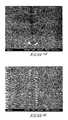
- FIG. 4is a scanning electron micrograph of an exemplary substrate surface that has not been treated in accordance with an aspect of the invention.
- FIG. 5is a scanning electron micrograph of an exemplary substrate surface that has resulted from treatment in accordance with an aspect of the invention.
- FIG. 6is a diagrammatic sectional view of a semiconductor wafer fragment at a processing step in accordance with an aspect of the invention.
- FIG. 1depicts a substrate 10 comprising a base substrate 12 and a layer 14 formed thereon.
- Base substrate 12might constitute a semiconductive substrate, for example bulk monocrystalline silicon material.
- semiconductor substrateor “semiconductive substrate” is defined to mean any construction comprising semiconductive material, including, but not limited to, bulk semiconductive materials such as a semiconductive wafer (either alone or in assemblies comprising other materials thereon), and semiconductive material layers (either alone or in assemblies comprising other materials).
- substraterefers to any supporting structure, including, but not limited to, the semiconductive substrates described above.
- layerencompasses both the singular and the plural unless otherwise indicated.
- Layer 14has been formed over base substrate 12 and comprises a first substrate surface 16 which, in the preferred embodiment, is outwardly exposed.
- First substrate surface 16comprises at least one of Pt, Pd, Co and Au in at least one of elemental and alloy forms.
- First substrate surface 16also has some first degree of roughness as either initially deposited or resulting from any subsequent processing. Accordingly in the context of this document, reference to “first degree of roughness” is to be interpreted temporally relative to a “second degree of roughness” described below, and not necessarily relative to a first ever or initial degree of roughness.
- the inventionwas initially reduced-to-practice in the fabrication of metal layers consisting essentially of elemental platinum.
- platinumwas deposited upon a substrate by atomic layer deposition.
- Suchencompasses the deposition of successive self-limiting monolayers over a substrate within a deposition chamber typically maintained at subatmospheric pressure.
- Successive mono-atomic layersare chemically adsorbed to a substrate and/or reacted with the outer layer on the substrate typically by the successive feeding of different deposition precursors to the substrate surface.
- the individual mono-atomic layersmight not completely cover a substrate surface or a portion of a substrate surface of intended deposition during a single deposition precursor feeding.
- the particular method for depositing the platinumutilized a platinum precursor comprising methylcyclopentadienyltrimethylplatinum (MeCpPt[Me] 3 ).
- a platinum precursorcomprising methylcyclopentadienyltrimethylplatinum (MeCpPt[Me] 3 ).
- Such precursorat a temperature of 45° C., was fed to a chamber within which the substrate was received over a 2 second period at a chamber pressure of about 1 ⁇ 10 ⁇ 3 Torr, with the substrate being at a temperature of 190° C. This was followed by approximately 2 seconds of not feeding any precursor or purge gas to the chamber, resulting in a chamber pressure of 1 ⁇ 10 ⁇ 6 Torr.
- Suchwas followed by a 1 second feed of O 2 at a pressure of 1 ⁇ 10 ⁇ 3 Torr, followed by a 2 second step in which no precursor or purge gas was fed to the chamber.
- Such individual cycleresulted in a platinum monolayer at least partially forming over the substrate.
- Repeating the sequencewas repeatedly conducted to result in the deposition of an exemplary layer 14 to a thickness of 500 Angstroms over some substrate 12 .
- Such a surface 14might constitute any one or combination of Pt, Pd, Co and Au, including in combination with any other metals, in at least one of elemental and alloy forms.
- substrate 10is provided within a suitable chamber 20 .
- Chamber 20is shown by example only, and might constitute a chamber within which layer 14 and/or outer surface 16 of the first degree of roughness is formed. Alternately, chamber 20 might constitute a different chamber.
- chamber 20is diagrammatically depicted as having gas inlets 22 and 24 , and an exhaust line 26 . Any chamber 20 is contemplated, whether existing or yet-to-be developed, and of course with any number of inlets, outlets, etc.
- first substrate surface 16is exposed to a PF 3 comprising atmosphere under conditions effective to form a second substrate surface 18 ( FIG.
- First substrate surface 16might be outwardly exposed during the PF 3 exposing. Alternately, the first substrate surface exposing might be through a thin or other layer formed over first substrate surface 16 and through which PF 3 can diffuse.
- the atmosphereconsists essentially of PF 3 . In another preferred embodiment, the atmosphere consists essentially of PF 3 and at least one of N 2 and a noble gas.
- the atmospheremight comprise plasma energized PF 3 , or alternately be void of plasma energized PF 3 . Further, if plasma generated PF 3 is utilized, such might be generated within chamber 20 or remotely therefrom. Further, any form of plasma generation is contemplated whether existing or yet-to-be developed. Regardless, where plasma generation is utilized, a preferred substrate temperature is from about 200° C. to about 450° C. (with from about 250° C. to about 350° C. being more preferred), and a preferred chamber pressure is less than or equal to about 2 Torr.
- an exemplary preferred substrate temperatureis from about 300° C. to about 500° C., with a preferred chamber pressure being less than or equal about 10 Torr.
- pressures at or above ambient room pressureare also contemplated, for example (and by way of example only) when above room ambient pressure at 5000 Torr and higher.
- FIG. 4depicts a scanning electron micrograph showing an exemplary first substrate surface of a first degree of roughness formed by the exemplary above-described atomic layer deposition method.
- FIG. 5depicts a different second substrate, although deposited using the above-described atomic layer deposition method, but after the above exemplary exposing to PF 3 resulting in a second degree of roughness that is perceptibly greater than the first degree of roughness.
- PF 3might be attacking the outer metal surface (M) forming a volatile M(PF 3 ) 4 species which leaves the surface. Further and yet, some of this volatile material might end up redepositing as the metal M. In another possibility, perhaps the PF 3 is attacking grain boundaries at the metal surface resulting in a roughening effect. Further, such might be a combination of these two theories, or other theories alone or in combination.
- the substrateAfter exposing the first substrate surface to a PF 3 comprising atmosphere, for example as described above, the substrate can be removed from the treating chamber. Some material might be formed over the substrate on (meaning in contact with) the second substrate surface having the second degree of roughness if such is outwardly exposed, and such material might be formed within the chamber of treatment prior to removing it therefrom, or in a different chamber. Alternately, no material might be subsequently formed on the second substrate surface having the second degree of roughness, depending upon the application.
- FIG. 6depicts an exemplary substrate 40 in the fabrication of a capacitor 42 .
- Substrate or wafer fragment 40comprises a first conductive capacitor electrode layer 14 which has been processed in the above-described exemplary manner to form a first capacitor electrode layer second surface 18 comprising at least one of Pt, Pd. Co and Au in at least one of elemental and alloy forms. All other exemplary preferred attributes as described above can be utilized in the fabrication of a capacitor in conjunction with the FIG. 6 construction.
- a capacitor dielectric layer 44is formed over capacitor electrode layer second surface 18 .
- An exemplary materialis Ta 2 O 5 .
- a second conductive capacitor electrode layer 46has been formed over capacitor dielectric layer 44 . Such might be the same or different in composition to that of layer 14 . Of course, multiple layers might constitute any of layers 14 , 44 and 46 in fabricating any exemplary existing or yet-to-be developed capacitor construction.
- One exemplary preferred capacitoris a metal-insulator-metal construction capacitor.
- the inventionhas applicability in methods of forming any substrate having some surface at least a portion of which comprises one of Pt, Pd, Co and Au in at least one of elemental and alloy forms.
- any substratehaving some surface at least a portion of which comprises one of Pt, Pd, Co and Au in at least one of elemental and alloy forms.
- such surfacesmight be utilized in automotive catalytic converters, fuel cells, and as heterogeneous catalysts in chemical processing.
Landscapes
- Chemical & Material Sciences (AREA)
- Chemical Kinetics & Catalysis (AREA)
- General Chemical & Material Sciences (AREA)
- Engineering & Computer Science (AREA)
- Materials Engineering (AREA)
- Electrochemistry (AREA)
- Mechanical Engineering (AREA)
- Metallurgy (AREA)
- Organic Chemistry (AREA)
- Physical Vapour Deposition (AREA)
- Internal Circuitry In Semiconductor Integrated Circuit Devices (AREA)
Abstract
Description
- This invention relates to methods of forming a substrate having a surface comprising at least one of Pt, Pd, Co and Au in at least one of elemental and alloy forms.
- Integrated circuits are typically formed on a semiconductor substrate such as a silicon wafer or other semiconducting material. In general, layers of various materials which are either semiconducting, conducting or insulating are utilized to form the integrated circuits. By way of example, the various materials are doped, ion implanted, deposited, etched, grown, etc. using various processes. A continuing goal in semiconductor processing is to reduce the size of individual electronic components thereby enabling smaller and denser integrated circuitry.
- One type of circuit device is a capacitor. As capacitors continue to get smaller, there is a continuing challenge to attain sufficient capacitance despite decreasing size. This has been approached both by developing improved materials and in the physical design of the capacitor, for example utilizing stacked and trenched constructions. A capacitor's capacitance is inherently a function of the amount of surface area between the electrodes and the capacitor dielectric region. Rougher surfaces have inherently higher surface areas than do smoother surfaces. Accordingly, increasing the degree of surface roughness of the capacitor electrodes is recognized as one way of facilitating maximum capacitance between an electrode and a capacitor dielectric region. This invention is directed to a method of increasing the surface roughness of certain metals.
- While the invention was motivated in addressing the above issues, it is in no way so limited. The invention is only limited by the accompanying claims as literally worded (without interpretative or other limiting reference to the above background art description, remaining portions of the specification or the drawings) and in accordance with the doctrine of equivalents.
- The invention includes methods of forming a substrate having a surface comprising at least one of Pt, Pd, Co and Au in at least one of elemental and alloy forms. In one implementation, a substrate is provided which has a first substrate surface comprising at least one of Pt, Pd, Co and Au in at least one of elemental and alloy forms. The first substrate surface has a first degree of roughness. Within a chamber, the first substrate surface is exposed to a PF3comprising atmosphere under conditions effective to form a second substrate surface comprising at least one of Pt, Pd, Co and Au in at least one of elemental and alloy forms which has a second degree of roughness which is greater than the first degree of roughness. The substrate having the second substrate surface with the second degree of roughness is ultimately removed from the chamber.
- Other aspects and implementations are contemplated.
- Preferred embodiments of the invention are described below with reference to the following accompanying drawings.
FIG. 1 is a diagrammatic sectional view of a semiconductor wafer fragment at a processing step in accordance with an aspect of the invention.FIG. 2 is a diagrammatic depiction of a processing chamber.FIG. 3 is a view of theFIG. 1 wafer fragment at a processing step subsequent to that depicted byFIG. 1 .FIG. 4 is a scanning electron micrograph of an exemplary substrate surface that has not been treated in accordance with an aspect of the invention.FIG. 5 is a scanning electron micrograph of an exemplary substrate surface that has resulted from treatment in accordance with an aspect of the invention.FIG. 6 is a diagrammatic sectional view of a semiconductor wafer fragment at a processing step in accordance with an aspect of the invention.- This disclosure of the invention is submitted in furtherance of the constitutional purposes of the U.S. Patent Laws “to promote the progress of science and useful arts” (Article 1, Section 8).
- By way of example only, first exemplary preferred embodiments of methods of forming a substrate having a surface comprising at least one of Pt, Pd, Co and Au in at least one of elemental and alloy forms are described initially with reference to
FIGS. 1-3 .FIG. 1 depicts asubstrate 10 comprising abase substrate 12 and alayer 14 formed thereon.Base substrate 12 might constitute a semiconductive substrate, for example bulk monocrystalline silicon material. In the context of this document, the term “semiconductor substrate” or “semiconductive substrate” is defined to mean any construction comprising semiconductive material, including, but not limited to, bulk semiconductive materials such as a semiconductive wafer (either alone or in assemblies comprising other materials thereon), and semiconductive material layers (either alone or in assemblies comprising other materials). The term “substrate” refers to any supporting structure, including, but not limited to, the semiconductive substrates described above. Also in the context of this document, the term “layer” encompasses both the singular and the plural unless otherwise indicated. Layer 14 has been formed overbase substrate 12 and comprises afirst substrate surface 16 which, in the preferred embodiment, is outwardly exposed.First substrate surface 16 comprises at least one of Pt, Pd, Co and Au in at least one of elemental and alloy forms.First substrate surface 16 also has some first degree of roughness as either initially deposited or resulting from any subsequent processing. Accordingly in the context of this document, reference to “first degree of roughness” is to be interpreted temporally relative to a “second degree of roughness” described below, and not necessarily relative to a first ever or initial degree of roughness.- The invention was initially reduced-to-practice in the fabrication of metal layers consisting essentially of elemental platinum. Such platinum was deposited upon a substrate by atomic layer deposition. Such encompasses the deposition of successive self-limiting monolayers over a substrate within a deposition chamber typically maintained at subatmospheric pressure. Successive mono-atomic layers are chemically adsorbed to a substrate and/or reacted with the outer layer on the substrate typically by the successive feeding of different deposition precursors to the substrate surface. The individual mono-atomic layers might not completely cover a substrate surface or a portion of a substrate surface of intended deposition during a single deposition precursor feeding. In accordance with the reduction-to-practice example, the particular method for depositing the platinum utilized a platinum precursor comprising methylcyclopentadienyltrimethylplatinum (MeCpPt[Me]3). Such precursor, at a temperature of 45° C., was fed to a chamber within which the substrate was received over a 2 second period at a chamber pressure of about 1×10⁻³Torr, with the substrate being at a temperature of 190° C. This was followed by approximately 2 seconds of not feeding any precursor or purge gas to the chamber, resulting in a chamber pressure of 1×10⁻⁶Torr. Such was followed by a 1 second feed of O2at a pressure of 1×10⁻³Torr, followed by a 2 second step in which no precursor or purge gas was fed to the chamber. Such individual cycle resulted in a platinum monolayer at least partially forming over the substrate. Repeating the sequence was repeatedly conducted to result in the deposition of an
exemplary layer 14 to a thickness of 500 Angstroms over somesubstrate 12. Such is provided by way of example only, with any other method of forming alayer 14 with anouter surface 16 being contemplated. Such asurface 14 might constitute any one or combination of Pt, Pd, Co and Au, including in combination with any other metals, in at least one of elemental and alloy forms. - In accordance with one implementation,
substrate 10 is provided within asuitable chamber 20.Chamber 20 is shown by example only, and might constitute a chamber within whichlayer 14 and/orouter surface 16 of the first degree of roughness is formed. Alternately,chamber 20 might constitute a different chamber. By way of example only,chamber 20 is diagrammatically depicted as havinggas inlets exhaust line 26. Anychamber 20 is contemplated, whether existing or yet-to-be developed, and of course with any number of inlets, outlets, etc. Withinchamber 20,first substrate surface 16 is exposed to a PF3comprising atmosphere under conditions effective to form a second substrate surface18 (FIG. 3 ) comprising at least one of Pt, Pd, Co and Au in at least one of elemental and alloy forms which has a second degree of roughness that is greater than the first degree of roughness.First substrate surface 16 might be outwardly exposed during the PF3exposing. Alternately, the first substrate surface exposing might be through a thin or other layer formed overfirst substrate surface 16 and through which PF3can diffuse. - In one preferred embodiment, the atmosphere consists essentially of PF3. In another preferred embodiment, the atmosphere consists essentially of PF3and at least one of N2and a noble gas. The atmosphere might comprise plasma energized PF3, or alternately be void of plasma energized PF3. Further, if plasma generated PF3is utilized, such might be generated within
chamber 20 or remotely therefrom. Further, any form of plasma generation is contemplated whether existing or yet-to-be developed. Regardless, where plasma generation is utilized, a preferred substrate temperature is from about 200° C. to about 450° C. (with from about 250° C. to about 350° C. being more preferred), and a preferred chamber pressure is less than or equal to about 2 Torr. Where the atmosphere is void of plasma energized PF3, an exemplary preferred substrate temperature is from about 300° C. to about 500° C., with a preferred chamber pressure being less than or equal about 10 Torr. However, pressures at or above ambient room pressure are also contemplated, for example (and by way of example only) when above room ambient pressure at 5000 Torr and higher. - The invention was reduced-to-practice in a 1 liter chamber using a sample substrate having an exposed
outer surface 16 of elemental platinum. The reactor was a custom laboratory chamber using remote inductively coupled plasma powered at 350 Watts. The only gas flowed to the chamber was PF3at room temperature at a flow rate of 50 sccm and providing an internal chamber pressure of 0.2 Torr. The substrate temperature was 300° C. The substrate was treated in this manner for 90 seconds. By way of example only,FIG. 4 depicts a scanning electron micrograph showing an exemplary first substrate surface of a first degree of roughness formed by the exemplary above-described atomic layer deposition method.FIG. 5 depicts a different second substrate, although deposited using the above-described atomic layer deposition method, but after the above exemplary exposing to PF3resulting in a second degree of roughness that is perceptibly greater than the first degree of roughness. - Without being limited by any theory of invention, the following are provided as examples or theories by which the roughening action might be occurring. In one possibility, PF3might be attacking the outer metal surface (M) forming a volatile M(PF3)4species which leaves the surface. Further and yet, some of this volatile material might end up redepositing as the metal M. In another possibility, perhaps the PF3is attacking grain boundaries at the metal surface resulting in a roughening effect. Further, such might be a combination of these two theories, or other theories alone or in combination.
- After exposing the first substrate surface to a PF3comprising atmosphere, for example as described above, the substrate can be removed from the treating chamber. Some material might be formed over the substrate on (meaning in contact with) the second substrate surface having the second degree of roughness if such is outwardly exposed, and such material might be formed within the chamber of treatment prior to removing it therefrom, or in a different chamber. Alternately, no material might be subsequently formed on the second substrate surface having the second degree of roughness, depending upon the application.
- The invention was motivated in the context of capacitor fabrication, and accordingly in using the second substrate surface in a capacitor. By way of example only,
FIG. 6 depicts anexemplary substrate 40 in the fabrication of acapacitor 42. Like numerals from the first described embodiment are utilized where appropriate, with differences being indicated with different numerals. Substrate orwafer fragment 40 comprises a first conductivecapacitor electrode layer 14 which has been processed in the above-described exemplary manner to form a first capacitor electrode layersecond surface 18 comprising at least one of Pt, Pd. Co and Au in at least one of elemental and alloy forms. All other exemplary preferred attributes as described above can be utilized in the fabrication of a capacitor in conjunction with theFIG. 6 construction. Acapacitor dielectric layer 44 is formed over capacitor electrode layersecond surface 18. An exemplary material is Ta2O5. A second conductivecapacitor electrode layer 46 has been formed overcapacitor dielectric layer 44. Such might be the same or different in composition to that oflayer 14. Of course, multiple layers might constitute any oflayers - While the invention was initially motivated from a desire to roughen certain surfaces in the fabrication of a capacitor, the invention is in no way so limited. Accordingly, the invention has applicability in methods of forming any substrate having some surface at least a portion of which comprises one of Pt, Pd, Co and Au in at least one of elemental and alloy forms. By way of example only, such surfaces might be utilized in automotive catalytic converters, fuel cells, and as heterogeneous catalysts in chemical processing.
- In compliance with the statute, the invention has been described in language more or less specific as to structural and methodical features. It is to be understood, however, that the invention is not limited to the specific features shown and described, since the means herein disclosed comprise preferred forms of putting the invention into effect. The invention is, therefore, claimed in any of its forms or modifications within the proper scope of the appended claims appropriately interpreted in accordance with the doctrine of equivalents.
Claims (30)
Priority Applications (1)
| Application Number | Priority Date | Filing Date | Title |
|---|---|---|---|
| US11/105,148US7271071B2 (en) | 2003-03-18 | 2005-04-12 | Method of forming a catalytic surface comprising at least one of Pt, Pd, Co and Au in at least one of elemental and alloy forms |
Applications Claiming Priority (2)
| Application Number | Priority Date | Filing Date | Title |
|---|---|---|---|
| US10/392,047US6884691B2 (en) | 2003-03-18 | 2003-03-18 | Method of forming a substrate having a surface comprising at least one of Pt, Pd, Co and Au in at least one of elemental and alloy forms |
| US11/105,148US7271071B2 (en) | 2003-03-18 | 2005-04-12 | Method of forming a catalytic surface comprising at least one of Pt, Pd, Co and Au in at least one of elemental and alloy forms |
Related Parent Applications (1)
| Application Number | Title | Priority Date | Filing Date |
|---|---|---|---|
| US10/392,047ContinuationUS6884691B2 (en) | 2003-03-18 | 2003-03-18 | Method of forming a substrate having a surface comprising at least one of Pt, Pd, Co and Au in at least one of elemental and alloy forms |
Publications (2)
| Publication Number | Publication Date |
|---|---|
| US20050191437A1true US20050191437A1 (en) | 2005-09-01 |
| US7271071B2 US7271071B2 (en) | 2007-09-18 |
Family
ID=32987820
Family Applications (2)
| Application Number | Title | Priority Date | Filing Date |
|---|---|---|---|
| US10/392,047Expired - LifetimeUS6884691B2 (en) | 2003-03-18 | 2003-03-18 | Method of forming a substrate having a surface comprising at least one of Pt, Pd, Co and Au in at least one of elemental and alloy forms |
| US11/105,148Expired - LifetimeUS7271071B2 (en) | 2003-03-18 | 2005-04-12 | Method of forming a catalytic surface comprising at least one of Pt, Pd, Co and Au in at least one of elemental and alloy forms |
Family Applications Before (1)
| Application Number | Title | Priority Date | Filing Date |
|---|---|---|---|
| US10/392,047Expired - LifetimeUS6884691B2 (en) | 2003-03-18 | 2003-03-18 | Method of forming a substrate having a surface comprising at least one of Pt, Pd, Co and Au in at least one of elemental and alloy forms |
Country Status (1)
| Country | Link |
|---|---|
| US (2) | US6884691B2 (en) |
Cited By (1)
| Publication number | Priority date | Publication date | Assignee | Title |
|---|---|---|---|---|
| US20170025324A1 (en)* | 2015-07-22 | 2017-01-26 | Tdk Corporation | Thin film capacitor and semiconductor device |
Families Citing this family (5)
| Publication number | Priority date | Publication date | Assignee | Title |
|---|---|---|---|---|
| US6884691B2 (en)* | 2003-03-18 | 2005-04-26 | Micron Technology, Inc. | Method of forming a substrate having a surface comprising at least one of Pt, Pd, Co and Au in at least one of elemental and alloy forms |
| US7259061B2 (en)* | 2004-07-15 | 2007-08-21 | Infineon Technologies Ag | Method for forming a capacitor for an integrated circuit and integrated circuit |
| JP2006190765A (en)* | 2005-01-05 | 2006-07-20 | Elpida Memory Inc | Semiconductor device and manufacturing method thereof |
| US8222127B2 (en)* | 2008-07-18 | 2012-07-17 | Micron Technology, Inc. | Methods of forming structures having nanotubes extending between opposing electrodes and structures including same |
| US8003521B2 (en) | 2009-04-07 | 2011-08-23 | Micron Technology, Inc. | Semiconductor processing |
Citations (26)
| Publication number | Priority date | Publication date | Assignee | Title |
|---|---|---|---|---|
| US5149854A (en)* | 1990-12-10 | 1992-09-22 | Mooney Chemicals, Inc. | Preparation of platinum group metal and rhenium carboxylates |
| US5431774A (en)* | 1993-11-30 | 1995-07-11 | Texas Instruments Incorporated | Copper etching |
| US5705443A (en)* | 1995-05-30 | 1998-01-06 | Advanced Technology Materials, Inc. | Etching method for refractory materials |
| US5990559A (en)* | 1998-08-27 | 1999-11-23 | Micron Technology, Inc. | Circuitry comprising roughened platinum layers, platinum-containing materials, capacitors comprising roughened platinum layers, methods forming roughened layers of platinum, and methods of forming capacitors |
| US6074945A (en)* | 1998-08-27 | 2000-06-13 | Micron Technology, Inc. | Methods for preparing ruthenium metal films |
| US6204178B1 (en)* | 1998-12-29 | 2001-03-20 | Micron Technology, Inc. | Nucleation and deposition of PT films using ultraviolet irradiation |
| US6204172B1 (en)* | 1998-09-03 | 2001-03-20 | Micron Technology, Inc. | Low temperature deposition of barrier layers |
| US6218297B1 (en)* | 1998-09-03 | 2001-04-17 | Micron Technology, Inc. | Patterning conductive metal layers and methods using same |
| US6271131B1 (en)* | 1998-08-26 | 2001-08-07 | Micron Technology, Inc. | Methods for forming rhodium-containing layers such as platinum-rhodium barrier layers |
| US6284655B1 (en)* | 1998-09-03 | 2001-09-04 | Micron Technology, Inc. | Method for producing low carbon/oxygen conductive layers |
| US6294425B1 (en)* | 1999-10-14 | 2001-09-25 | Samsung Electronics Co., Ltd. | Methods of forming integrated circuit capacitors by electroplating electrodes from seed layers |
| US6318381B1 (en)* | 1999-07-13 | 2001-11-20 | Micron Technology, Inc. | Methods of cleaning vaporization surfaces |
| US6429071B1 (en)* | 1996-05-17 | 2002-08-06 | Micron Technology, Inc. | Method of increasing capacitance of memory cells incorporating hemispherical grained silicon |
| US6517616B2 (en)* | 1998-08-27 | 2003-02-11 | Micron Technology, Inc. | Solvated ruthenium precursors for direct liquid injection of ruthenium and ruthenium oxide |
| US6528786B2 (en)* | 1998-03-05 | 2003-03-04 | Micron Technology, Inc. | Analysis of semiconductor surfaces by secondary ion mass spectrometry and methods |
| US6541067B1 (en)* | 1998-08-27 | 2003-04-01 | Micron Technology, Inc. | Solvated ruthenium precursors for direct liquid injection of ruthenium and ruthenium oxide and method of using same |
| US6569689B2 (en)* | 1999-03-01 | 2003-05-27 | Micron Technology, Inc. | Method of forming a capacitor |
| US6635561B2 (en)* | 2001-01-26 | 2003-10-21 | Mitsubishi Denki Kabushiki Kaisha | Semiconductor device, and method of manufacturing the semiconductor device |
| US6642567B1 (en)* | 2000-08-31 | 2003-11-04 | Micron Technology, Inc. | Devices containing zirconium-platinum-containing materials and methods for preparing such materials and devices |
| US6660631B1 (en)* | 2000-08-31 | 2003-12-09 | Micron Technology, Inc. | Devices containing platinum-iridium films and methods of preparing such films and devices |
| US6673701B1 (en)* | 2002-08-27 | 2004-01-06 | Micron Technology, Inc. | Atomic layer deposition methods |
| US6677252B2 (en)* | 1998-10-22 | 2004-01-13 | Micron Technology, Inc. | Methods for planarization of non-planar surfaces in device fabrication |
| US6737313B1 (en)* | 2003-04-16 | 2004-05-18 | Micron Technology, Inc. | Surface treatment of an oxide layer to enhance adhesion of a ruthenium metal layer |
| US6783657B2 (en)* | 2002-08-29 | 2004-08-31 | Micron Technology, Inc. | Systems and methods for the electrolytic removal of metals from substrates |
| US6884691B2 (en)* | 2003-03-18 | 2005-04-26 | Micron Technology, Inc. | Method of forming a substrate having a surface comprising at least one of Pt, Pd, Co and Au in at least one of elemental and alloy forms |
| US7041570B2 (en)* | 1999-04-06 | 2006-05-09 | Micron Technology, Inc. | Method of forming a capacitor |
- 2003
- 2003-03-18USUS10/392,047patent/US6884691B2/ennot_activeExpired - Lifetime
- 2005
- 2005-04-12USUS11/105,148patent/US7271071B2/ennot_activeExpired - Lifetime
Patent Citations (33)
| Publication number | Priority date | Publication date | Assignee | Title |
|---|---|---|---|---|
| US5149854A (en)* | 1990-12-10 | 1992-09-22 | Mooney Chemicals, Inc. | Preparation of platinum group metal and rhenium carboxylates |
| US5431774A (en)* | 1993-11-30 | 1995-07-11 | Texas Instruments Incorporated | Copper etching |
| US5705443A (en)* | 1995-05-30 | 1998-01-06 | Advanced Technology Materials, Inc. | Etching method for refractory materials |
| US6429071B1 (en)* | 1996-05-17 | 2002-08-06 | Micron Technology, Inc. | Method of increasing capacitance of memory cells incorporating hemispherical grained silicon |
| US6528786B2 (en)* | 1998-03-05 | 2003-03-04 | Micron Technology, Inc. | Analysis of semiconductor surfaces by secondary ion mass spectrometry and methods |
| US6271131B1 (en)* | 1998-08-26 | 2001-08-07 | Micron Technology, Inc. | Methods for forming rhodium-containing layers such as platinum-rhodium barrier layers |
| US6690055B1 (en)* | 1998-08-26 | 2004-02-10 | Micron Technology, Inc. | Devices containing platinum-rhodium layers and methods |
| US6074945A (en)* | 1998-08-27 | 2000-06-13 | Micron Technology, Inc. | Methods for preparing ruthenium metal films |
| US6583022B1 (en)* | 1998-08-27 | 2003-06-24 | Micron Technology, Inc. | Methods of forming roughened layers of platinum and methods of forming capacitors |
| US6281161B1 (en)* | 1998-08-27 | 2001-08-28 | Micron Technology, Inc. | Platinum-containing materials and catalysts |
| US6541067B1 (en)* | 1998-08-27 | 2003-04-01 | Micron Technology, Inc. | Solvated ruthenium precursors for direct liquid injection of ruthenium and ruthenium oxide and method of using same |
| US5990559A (en)* | 1998-08-27 | 1999-11-23 | Micron Technology, Inc. | Circuitry comprising roughened platinum layers, platinum-containing materials, capacitors comprising roughened platinum layers, methods forming roughened layers of platinum, and methods of forming capacitors |
| US6517616B2 (en)* | 1998-08-27 | 2003-02-11 | Micron Technology, Inc. | Solvated ruthenium precursors for direct liquid injection of ruthenium and ruthenium oxide |
| US6284655B1 (en)* | 1998-09-03 | 2001-09-04 | Micron Technology, Inc. | Method for producing low carbon/oxygen conductive layers |
| US6403414B2 (en)* | 1998-09-03 | 2002-06-11 | Micron Technology, Inc. | Method for producing low carbon/oxygen conductive layers |
| US6323511B1 (en)* | 1998-09-03 | 2001-11-27 | Micron Technology, Inc. | Structures including low carbon/oxygen conductive layers |
| US6495458B2 (en)* | 1998-09-03 | 2002-12-17 | Micron Technology, Inc. | Method for producing low carbon/oxygen conductive layers |
| US6204172B1 (en)* | 1998-09-03 | 2001-03-20 | Micron Technology, Inc. | Low temperature deposition of barrier layers |
| US6218297B1 (en)* | 1998-09-03 | 2001-04-17 | Micron Technology, Inc. | Patterning conductive metal layers and methods using same |
| US6677252B2 (en)* | 1998-10-22 | 2004-01-13 | Micron Technology, Inc. | Methods for planarization of non-planar surfaces in device fabrication |
| US6387802B1 (en)* | 1998-12-29 | 2002-05-14 | Micron Technology, Inc. | Nucleation and deposition of Pt films using ultraviolet irradiation |
| US6204178B1 (en)* | 1998-12-29 | 2001-03-20 | Micron Technology, Inc. | Nucleation and deposition of PT films using ultraviolet irradiation |
| US6569689B2 (en)* | 1999-03-01 | 2003-05-27 | Micron Technology, Inc. | Method of forming a capacitor |
| US7041570B2 (en)* | 1999-04-06 | 2006-05-09 | Micron Technology, Inc. | Method of forming a capacitor |
| US6318381B1 (en)* | 1999-07-13 | 2001-11-20 | Micron Technology, Inc. | Methods of cleaning vaporization surfaces |
| US6294425B1 (en)* | 1999-10-14 | 2001-09-25 | Samsung Electronics Co., Ltd. | Methods of forming integrated circuit capacitors by electroplating electrodes from seed layers |
| US6660631B1 (en)* | 2000-08-31 | 2003-12-09 | Micron Technology, Inc. | Devices containing platinum-iridium films and methods of preparing such films and devices |
| US6642567B1 (en)* | 2000-08-31 | 2003-11-04 | Micron Technology, Inc. | Devices containing zirconium-platinum-containing materials and methods for preparing such materials and devices |
| US6635561B2 (en)* | 2001-01-26 | 2003-10-21 | Mitsubishi Denki Kabushiki Kaisha | Semiconductor device, and method of manufacturing the semiconductor device |
| US6673701B1 (en)* | 2002-08-27 | 2004-01-06 | Micron Technology, Inc. | Atomic layer deposition methods |
| US6783657B2 (en)* | 2002-08-29 | 2004-08-31 | Micron Technology, Inc. | Systems and methods for the electrolytic removal of metals from substrates |
| US6884691B2 (en)* | 2003-03-18 | 2005-04-26 | Micron Technology, Inc. | Method of forming a substrate having a surface comprising at least one of Pt, Pd, Co and Au in at least one of elemental and alloy forms |
| US6737313B1 (en)* | 2003-04-16 | 2004-05-18 | Micron Technology, Inc. | Surface treatment of an oxide layer to enhance adhesion of a ruthenium metal layer |
Cited By (2)
| Publication number | Priority date | Publication date | Assignee | Title |
|---|---|---|---|---|
| US20170025324A1 (en)* | 2015-07-22 | 2017-01-26 | Tdk Corporation | Thin film capacitor and semiconductor device |
| US10121728B2 (en)* | 2015-07-22 | 2018-11-06 | Tdk Corporation | Thin film capacitor and semiconductor device with improved heat dissipation |
Also Published As
| Publication number | Publication date |
|---|---|
| US6884691B2 (en) | 2005-04-26 |
| US7271071B2 (en) | 2007-09-18 |
| US20040185636A1 (en) | 2004-09-23 |
Similar Documents
| Publication | Publication Date | Title |
|---|---|---|
| KR100451486B1 (en) | Methods of forming roughened layers of platinum | |
| US7112503B1 (en) | Enhanced surface area capacitor fabrication methods | |
| US7217615B1 (en) | Capacitor fabrication methods including forming a conductive layer | |
| US5733816A (en) | Method for depositing a tungsten layer on silicon | |
| US20080200019A9 (en) | Selective Deposition of Noble Metal Thin Films | |
| US7741175B2 (en) | Methods of forming capacitors | |
| US6884691B2 (en) | Method of forming a substrate having a surface comprising at least one of Pt, Pd, Co and Au in at least one of elemental and alloy forms | |
| WO2011159691A2 (en) | Chemical vapor deposition of ruthenium films containing oxygen or carbon | |
| US6723599B2 (en) | Methods of forming capacitors and methods of forming capacitor dielectric layers | |
| US6924195B2 (en) | Methods of forming metal-comprising materials and capacitor electrodes; and capacitor constructions | |
| KR100588888B1 (en) | Manufacturing method of capacitor having tantalum oxide film as insulating film | |
| US20060249229A1 (en) | Metal layer forming methods and capacitor electrode forming methods | |
| US7435678B2 (en) | Method of depositing noble metal electrode using oxidation-reduction reaction |
Legal Events
| Date | Code | Title | Description |
|---|---|---|---|
| FEPP | Fee payment procedure | Free format text:PAYOR NUMBER ASSIGNED (ORIGINAL EVENT CODE: ASPN); ENTITY STATUS OF PATENT OWNER: LARGE ENTITY | |
| STCF | Information on status: patent grant | Free format text:PATENTED CASE | |
| CC | Certificate of correction | ||
| FPAY | Fee payment | Year of fee payment:4 | |
| FPAY | Fee payment | Year of fee payment:8 | |
| AS | Assignment | Owner name:U.S. BANK NATIONAL ASSOCIATION, AS COLLATERAL AGENT, CALIFORNIA Free format text:SECURITY INTEREST;ASSIGNOR:MICRON TECHNOLOGY, INC.;REEL/FRAME:038669/0001 Effective date:20160426 Owner name:U.S. BANK NATIONAL ASSOCIATION, AS COLLATERAL AGEN Free format text:SECURITY INTEREST;ASSIGNOR:MICRON TECHNOLOGY, INC.;REEL/FRAME:038669/0001 Effective date:20160426 | |
| AS | Assignment | Owner name:MORGAN STANLEY SENIOR FUNDING, INC., AS COLLATERAL AGENT, MARYLAND Free format text:PATENT SECURITY AGREEMENT;ASSIGNOR:MICRON TECHNOLOGY, INC.;REEL/FRAME:038954/0001 Effective date:20160426 Owner name:MORGAN STANLEY SENIOR FUNDING, INC., AS COLLATERAL Free format text:PATENT SECURITY AGREEMENT;ASSIGNOR:MICRON TECHNOLOGY, INC.;REEL/FRAME:038954/0001 Effective date:20160426 | |
| AS | Assignment | Owner name:U.S. BANK NATIONAL ASSOCIATION, AS COLLATERAL AGENT, CALIFORNIA Free format text:CORRECTIVE ASSIGNMENT TO CORRECT THE REPLACE ERRONEOUSLY FILED PATENT #7358718 WITH THE CORRECT PATENT #7358178 PREVIOUSLY RECORDED ON REEL 038669 FRAME 0001. ASSIGNOR(S) HEREBY CONFIRMS THE SECURITY INTEREST;ASSIGNOR:MICRON TECHNOLOGY, INC.;REEL/FRAME:043079/0001 Effective date:20160426 Owner name:U.S. BANK NATIONAL ASSOCIATION, AS COLLATERAL AGEN Free format text:CORRECTIVE ASSIGNMENT TO CORRECT THE REPLACE ERRONEOUSLY FILED PATENT #7358718 WITH THE CORRECT PATENT #7358178 PREVIOUSLY RECORDED ON REEL 038669 FRAME 0001. ASSIGNOR(S) HEREBY CONFIRMS THE SECURITY INTEREST;ASSIGNOR:MICRON TECHNOLOGY, INC.;REEL/FRAME:043079/0001 Effective date:20160426 | |
| AS | Assignment | Owner name:JPMORGAN CHASE BANK, N.A., AS COLLATERAL AGENT, ILLINOIS Free format text:SECURITY INTEREST;ASSIGNORS:MICRON TECHNOLOGY, INC.;MICRON SEMICONDUCTOR PRODUCTS, INC.;REEL/FRAME:047540/0001 Effective date:20180703 Owner name:JPMORGAN CHASE BANK, N.A., AS COLLATERAL AGENT, IL Free format text:SECURITY INTEREST;ASSIGNORS:MICRON TECHNOLOGY, INC.;MICRON SEMICONDUCTOR PRODUCTS, INC.;REEL/FRAME:047540/0001 Effective date:20180703 | |
| AS | Assignment | Owner name:MICRON TECHNOLOGY, INC., IDAHO Free format text:RELEASE BY SECURED PARTY;ASSIGNOR:U.S. BANK NATIONAL ASSOCIATION, AS COLLATERAL AGENT;REEL/FRAME:047243/0001 Effective date:20180629 | |
| MAFP | Maintenance fee payment | Free format text:PAYMENT OF MAINTENANCE FEE, 12TH YEAR, LARGE ENTITY (ORIGINAL EVENT CODE: M1553); ENTITY STATUS OF PATENT OWNER: LARGE ENTITY Year of fee payment:12 | |
| AS | Assignment | Owner name:MICRON TECHNOLOGY, INC., IDAHO Free format text:RELEASE BY SECURED PARTY;ASSIGNOR:MORGAN STANLEY SENIOR FUNDING, INC., AS COLLATERAL AGENT;REEL/FRAME:050937/0001 Effective date:20190731 | |
| AS | Assignment | Owner name:MICRON SEMICONDUCTOR PRODUCTS, INC., IDAHO Free format text:RELEASE BY SECURED PARTY;ASSIGNOR:JPMORGAN CHASE BANK, N.A., AS COLLATERAL AGENT;REEL/FRAME:051028/0001 Effective date:20190731 Owner name:MICRON TECHNOLOGY, INC., IDAHO Free format text:RELEASE BY SECURED PARTY;ASSIGNOR:JPMORGAN CHASE BANK, N.A., AS COLLATERAL AGENT;REEL/FRAME:051028/0001 Effective date:20190731 |