US20050190587A1 - Microstrip line dielectric overlay - Google Patents
Microstrip line dielectric overlayDownload PDFInfo
- Publication number
- US20050190587A1 US20050190587A1US10/789,931US78993104AUS2005190587A1US 20050190587 A1US20050190587 A1US 20050190587A1US 78993104 AUS78993104 AUS 78993104AUS 2005190587 A1US2005190587 A1US 2005190587A1
- Authority
- US
- United States
- Prior art keywords
- microstrip line
- circuit board
- dielectric constant
- dielectric
- printed circuit
- Prior art date
- Legal status (The legal status is an assumption and is not a legal conclusion. Google has not performed a legal analysis and makes no representation as to the accuracy of the status listed.)
- Granted
Links
- 238000000576coating methodMethods0.000claimsabstractdescription63
- 239000011248coating agentSubstances0.000claimsabstractdescription62
- 239000000463materialSubstances0.000claimsabstractdescription32
- 230000005684electric fieldEffects0.000claimsdescription27
- 239000000758substrateSubstances0.000claimsdescription24
- 230000008859changeEffects0.000claimsdescription15
- 239000011152fibreglassSubstances0.000claimsdescription11
- 238000000034methodMethods0.000claims16
- 238000004519manufacturing processMethods0.000claims1
- 239000004020conductorSubstances0.000description25
- 229920001343polytetrafluoroethylenePolymers0.000description6
- 239000004810polytetrafluoroethyleneSubstances0.000description6
- 230000000694effectsEffects0.000description5
- 230000005540biological transmissionEffects0.000description4
- RYGMFSIKBFXOCR-UHFFFAOYSA-NCopperChemical compound[Cu]RYGMFSIKBFXOCR-UHFFFAOYSA-N0.000description3
- 229910052802copperInorganic materials0.000description3
- 239000010949copperSubstances0.000description3
- 230000008878couplingEffects0.000description3
- 238000010168coupling processMethods0.000description3
- 238000005859coupling reactionMethods0.000description3
- 230000001902propagating effectEffects0.000description3
- 230000006641stabilisationEffects0.000description2
- 238000011105stabilizationMethods0.000description2
- 230000007704transitionEffects0.000description2
- 239000004809TeflonSubstances0.000description1
- 229920006362Teflon®Polymers0.000description1
- 230000006978adaptationEffects0.000description1
- 229910052782aluminiumInorganic materials0.000description1
- XAGFODPZIPBFFR-UHFFFAOYSA-NaluminiumChemical compound[Al]XAGFODPZIPBFFR-UHFFFAOYSA-N0.000description1
- 230000003466anti-cipated effectEffects0.000description1
- 238000013459approachMethods0.000description1
- 230000008901benefitEffects0.000description1
- 230000001808coupling effectEffects0.000description1
- 230000001419dependent effectEffects0.000description1
- 230000006872improvementEffects0.000description1
- 230000001939inductive effectEffects0.000description1
- 229910052751metalInorganic materials0.000description1
- 239000002184metalSubstances0.000description1
- 239000000203mixtureSubstances0.000description1
- -1polytetrafluoroethylenePolymers0.000description1
- 230000009467reductionEffects0.000description1
- 229910052709silverInorganic materials0.000description1
- 239000004332silverSubstances0.000description1
Images


Classifications
- H—ELECTRICITY
- H01—ELECTRIC ELEMENTS
- H01P—WAVEGUIDES; RESONATORS, LINES, OR OTHER DEVICES OF THE WAVEGUIDE TYPE
- H01P3/00—Waveguides; Transmission lines of the waveguide type
- H01P3/02—Waveguides; Transmission lines of the waveguide type with two longitudinal conductors
- H01P3/08—Microstrips; Strip lines
- H01P3/081—Microstriplines
- H—ELECTRICITY
- H05—ELECTRIC TECHNIQUES NOT OTHERWISE PROVIDED FOR
- H05K—PRINTED CIRCUITS; CASINGS OR CONSTRUCTIONAL DETAILS OF ELECTRIC APPARATUS; MANUFACTURE OF ASSEMBLAGES OF ELECTRICAL COMPONENTS
- H05K1/00—Printed circuits
- H05K1/02—Details
- H05K1/0213—Electrical arrangements not otherwise provided for
- H05K1/0237—High frequency adaptations
- H05K1/024—Dielectric details, e.g. changing the dielectric material around a transmission line
- H—ELECTRICITY
- H05—ELECTRIC TECHNIQUES NOT OTHERWISE PROVIDED FOR
- H05K—PRINTED CIRCUITS; CASINGS OR CONSTRUCTIONAL DETAILS OF ELECTRIC APPARATUS; MANUFACTURE OF ASSEMBLAGES OF ELECTRICAL COMPONENTS
- H05K3/00—Apparatus or processes for manufacturing printed circuits
- H05K3/22—Secondary treatment of printed circuits
- H05K3/28—Applying non-metallic protective coatings
- H—ELECTRICITY
- H05—ELECTRIC TECHNIQUES NOT OTHERWISE PROVIDED FOR
- H05K—PRINTED CIRCUITS; CASINGS OR CONSTRUCTIONAL DETAILS OF ELECTRIC APPARATUS; MANUFACTURE OF ASSEMBLAGES OF ELECTRICAL COMPONENTS
- H05K2201/00—Indexing scheme relating to printed circuits covered by H05K1/00
- H05K2201/09—Shape and layout
- H05K2201/09209—Shape and layout details of conductors
- H05K2201/09218—Conductive traces
- H05K2201/09236—Parallel layout
- Y—GENERAL TAGGING OF NEW TECHNOLOGICAL DEVELOPMENTS; GENERAL TAGGING OF CROSS-SECTIONAL TECHNOLOGIES SPANNING OVER SEVERAL SECTIONS OF THE IPC; TECHNICAL SUBJECTS COVERED BY FORMER USPC CROSS-REFERENCE ART COLLECTIONS [XRACs] AND DIGESTS
- Y10—TECHNICAL SUBJECTS COVERED BY FORMER USPC
- Y10T—TECHNICAL SUBJECTS COVERED BY FORMER US CLASSIFICATION
- Y10T29/00—Metal working
- Y10T29/49—Method of mechanical manufacture
- Y10T29/49002—Electrical device making
- Y10T29/49016—Antenna or wave energy "plumbing" making
- Y—GENERAL TAGGING OF NEW TECHNOLOGICAL DEVELOPMENTS; GENERAL TAGGING OF CROSS-SECTIONAL TECHNOLOGIES SPANNING OVER SEVERAL SECTIONS OF THE IPC; TECHNICAL SUBJECTS COVERED BY FORMER USPC CROSS-REFERENCE ART COLLECTIONS [XRACs] AND DIGESTS
- Y10—TECHNICAL SUBJECTS COVERED BY FORMER USPC
- Y10T—TECHNICAL SUBJECTS COVERED BY FORMER US CLASSIFICATION
- Y10T29/00—Metal working
- Y10T29/49—Method of mechanical manufacture
- Y10T29/49002—Electrical device making
- Y10T29/49117—Conductor or circuit manufacturing
- Y10T29/49124—On flat or curved insulated base, e.g., printed circuit, etc.
- Y10T29/49155—Manufacturing circuit on or in base
Definitions
- the inventionrelates generally to printed circuit boards, and more specifically to dielectric overlay on microstrip printed circuit strips.
- Electronic devicestypically include circuits assembled from components that are soldered to conductive traces on a printed circuit board.
- the boarditself is formed of a material such as fiberglass, and has conductive copper traces running along at least one plane of the circuit board.
- Sophisticated circuit boardsoften have several layers of traces, including layers on the top and bottom side of the circuit board and embedded within the circuit board. These various traces connect components to one another, and distribute signals such as power, ground, and clock signals throughout the circuit board.
- the dielectric constantalso known as the relative permittivity
- This constantdescribes the way in which an electric field penetrates a specific material relative to free air. It is also important for understanding how fast a signal travels in a conductor, as propagation delay of a signal in a conductor is proportional to the square root of the dielectric constant.
- the propagation delay of a signal traveling through a conductor in airis approximately 85 picoseconds per inch
- the dielectric constant of fiberglass printed circuit boardsis approximately 4.5, meaning that a signal propagating on a conductive circuit trace entirely within the FR4 material known as a stripline experiences a delay of the square root of 4.5 multiplied by 85 picoseconds per inch, or approximately 180 picoseconds per inch.
- Circuit traces on the top and bottom surfaces of the FR4 circuit boardare known as microstrips, and because they are surrounded by a combination of free space and FR4 material, experience an effective dielectric constant of about 2.8, resulting in a propagation delay of approximately 140 picoseconds per inch.
- a circuit designercan account for these differences in laying out conductive traces on and within a printed circuit board, ensuring that signals take a desired or known time to travel between components.
- the situationis complicated, however, when various outside forces cause the electric fields surrounding a conductor to vary in configuration, resulting in a changing effective dielectric constant around a microstrip line as a circuit operates.
- One example of such a circumstancecan occur when two microstrip lines run parallel and near to one another on a surface of a circuit board above a ground plane within the circuit board.
- the conductorsare carrying signals near one another in voltage or potential (known as even mode)
- the electric field surrounding each conductoris spatially different in than when the two conductors are carrying signals of different voltages (known as odd mode).
- odd modeWhen the conductors are at differing potentials, a greater portion of the electric field resides in free space, resulting in a reduction in propagation delay.
- the change in propagation delay with changed signal modealso results in a significant increase in crosstalk between conductors as observed at the receiving or far end of the conductors, which is also undesirable.
- FIG. 1illustrates a cutaway view of a pair of stripline conductors within a printed circuit board, consistent with the prior art.
- FIG. 2shows a cutaway view of a pair of microstrip line conductors on a printed circuit board, consistent with the prior art.
- FIG. 3shows a pair of adjacent microstrip lines mounted on a printed circuit board connecting a signal generating integrated circuit to a signal receiving integrated circuit, consistent with an embodiment of the present invention.
- FIG. 4shows a an eye pattern illustrating jitter in a stripline, consistent with the prior art.
- FIG. 5shows an eye pattern illustrating jitter in a microstrip line, consistent with the prior art.
- FIG. 6illustrates a pair of adjacent microstrip lines with a dielectric coating, consistent with the present invention.
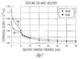
- FIG. 7illustrates the difference in even-mode and odd-mode velocities with various dielectric overcoat thicknesses, consistent with an embodiment of the present invention.
- the present inventionprovides in one embodiment a printed circuit board having a dielectric constant different from the dielectric constant of free space, with at least two microstrip lines routed adjacent to one another on a surface of the printed circuit board.
- a dielectric coatingis applied to at least one of the at least two microstrip lines such that the dielectric constant of the dielectric coating differs from the dielectric constant of free space.
- the dielectric coatingcomprises a material having a dielectric constant approximately equal to the dielectric constant of the printed circuit board.
- the present inventionin some embodiments reduces the change in propagation delay between even and odd mode signals in microstrip lines.
- two microstrip linesare routed on the same surface of a printed circuit board near enough one another that their electric fields influence one another when the microstrip lines carry electric signals.
- a dielectric coatingis applied to at least a first one of the two microstrip lines, where the dielectric coating has a dielectric constant greater than one, or greater than the dielectric constant of free space.
- the applied dielectric coatingreduces the change in dielectric constant seen by the first microstrip line when the signals in the microstrip lines change, reducing the change in propagation delay experienced by the first microstrip line.
- the net effectis that far-end observed crosstalk between the lines is substantially reduced, as is observed jitter, due to the in-phase nature of the signals propagating down adjacent lines.
- FIG. 1shows a typical pair of striplines, consistent with the prior art.
- the stirplines 101 and 102are routed through the circuit board material 103 , which in some embodiments is an FR-4 fiberglass circuit board having a dielectric constant of approximately 4.2-4.5.
- the conductive traces 101 and 102are seen here from an end view, and will typically run a fraction of an inch to many inches to connect one electrical component to another.
- the composition of conductive traces 101 and 102is typically copper, but can in other embodiments be any other suitable conductor, such as aluminum, silver, or another metal.
- the electric field of conductor 102will influence the electric field of conductor 101 .
- the change in spatial configuration of the electric fieldwill have relatively little effect on the effective dielectric constant of surrounding material as seen by the stripline 101 , however, as the electric field will remain within the FR4 circuit board material 103 .
- Circumstancesare different in the case of a pair of microstrip line conductors as shown in FIG. 2 , consistent with the prior art.
- the microstrip line conductors 201 and 202are similarly routed adjacent to one another, but are routed on the surface of the printed circuit board 203 .
- the circuit boardhas the same dielectric constant of approximately 4.2-4.5, but the electric field surrounding conductor 201 is partly in free space, which has a dielectric constant of 1.0, and partly in the circuit board 203 . This results in an effective dielectric constant as seen by the microstrip line 201 of some value between that of free space and the dielectric constant of the circuit board.
- the dielectric constant of material surrounding a conductoris important to propagation of a signal in that the speed the signal travels is inversely proportional to the square root of the effective dielectric constant seen by the conductor's electric field.
- the propagation velocity of a signal in the microstrip line of FIG. 2is therefore faster than the propagation of the same signal in the stripline of FIG. 1 , because the dielectric constant of the fiberglass board in FIG. 1 that contains nearly all the electric field is larger than the effective dielectric constant seen by the microstrip lines of FIG. 2 , which have a lower effective dielectric constant due to the portion of the electric field that travels in free space.
- some engineersrefer to the propagation velocity of the signal in terms of propagation delay, as is explained in greater detail in the background.
- a first integrated circuit 302generates two signals sent to integrated circuit 303 via microstrip lines 304 and 305 .
- the electric fields between the linescreate capacitive coupling between lines, in addition to other coupling effects such as inductive coupling between the lines.
- This couplingcan result in observed far-end crosstalk between the lines, where a portion of the signal sent on microstrip line 304 is observed on microstrip line 305 , and a portion of the signal sent on microstrip line 305 can be observed on microstrip line 304 at the receiving integrated circuit 303 .
- FIGS. 4 and 5illustrate the difference in jitter that can be observed in a typical case between similar microstrip and striplines, as a result of differences in potential between two adjacent lines.
- FIG. 4shows that for striplines such as in FIG. 1 , a jitter of 14 picoseconds is observed, and all observed signal transitions are grouped relatively tightly together in time.
- the microstrip line eye chart of FIG. 5shows an average jitter figure of 95 picoseconds, and shows three distinct timing groupings for signals transitioning from low to high, and three distinct timing groupings for signals traveling from high to low.
- These three groupingsrepresent the cases in which the measured microstrip line is transitioning to lower potential than the adjacent line, where the measured microstrip line is transitioning to the same potential as the adjacent line, and where the measured microstrip line is transitioning to a higher potential than the adjacent microstrip line. Because the electric field around the microstrip line being measured is configured differently for each of the three cases, the effective dielectric constant it observes, and the resulting propagation delay of a signal along the microstrip line, changes for each case.
- the present inventionseeks to reduce the far-end observed effects such as crosstalk and jitter by adding a dielectric coating to the top side of such microstrip lines, as is shown in FIG. 6 .
- a 5 mil FR4 fiberglass material having a dielectric constant of approximately 4.2separates a ground plane 602 from adjacent microstrip lines 603 and 604 .
- a dielectric coating 605is applied in a thickness of 8.2 mils, which is calculated to produce a stable effective dielectric constant observed by the microstrip lines, and make the propagation velocities of signals in the microstrip lines substantially the same under varying signal conditions.
- Various embodiments of the inventionwill have various thicknesses of dielectric overcoat, which in some embodiments will be dependent on the spacing between the microstrip line and the ground plane, between the microstrip line and an adjacent microstrip line, or some combination thereof.
- a dielectric coatmay be applied at 0.5, 0.75, 1, 1.25, 1.5, or some other multiple thickness relative to the distance between the microstrip line and the ground plane.
- these specified thicknesseswill be minimum thicknesses rather than target thicknesses.
- the overcoat material 605is desirably of the same or relatively similar dielectric constant as the substrate 605 , to minimize the change in effective dielectric constant and in resulting propagation delay when the electric field around a microstrip line changes in spatial configuration.
- a dielectric overcoat material having the same dielectric constantBy using a dielectric overcoat material having the same dielectric constant, such changes in effective dielectric constant and propagation delay can be nearly eliminated.
- the thickness of the dielectric overcoat materialwill be a compromise between being thick enough to contain most all of the electric field surrounding microstrip lines 603 and 604 , and being thin enough to be physically practical and cost-effective. It should be noted, however, that any dielectric overcoat material having a dielectric constant greater than that of free space within reason at even a modest thickness will result in some improvement in far-end observed crosstalk and jitter.
- FIG. 7illustrates the difference in even-mode and odd-mode velocities with various dielectric overcoat thicknesses, consistent with an embodiment of the present invention.
- the resulting even and odd mode propagation velocities shown herewill change with geometry and materials used in constructing the microstrip lines, but serves to illustrate the effectiveness of an 8.2 mil dielectric overcoat over microstrip lines on a 5 mil FR4 board, where the dielectric constant of the overcoat and the FR4 board are both approximately 4.2, such as was shown and discussed in conjunction with FIG. 6 .
- Trace 701shows how the propagation velocity changes for even mode signals in the microstrip lines of FIG. 6 as the thickness of the dielectric overcoat is changed, while trace 702 shows how odd mode propagation velocities vary as the dielectric overcoat thickness changes.
- trace 702shows how odd mode propagation velocities vary as the dielectric overcoat thickness changes.
- TeflonTrademark of DuPont
- PTFEpolytetrafluoroethylene
- This materialis sometimes used because its low dielectric constant results in a relatively low propagation delay for stripline and microstrip lines, resulting in a relatively high performance circuit board. Because additional cost of the PTFE material is expended to achieve high performance in critical applications, it is anticipated that a dielectric overlay material applied to microstrip lines routed on PTFE substrates will be of substantial benefit to a PTFE circuit board designer.
- the dielectric overlay materialwill ideally have a dielectric constant near 2.0.
- the end resultwill be a microstrip line in which the signals travel (sqrt(2.0)/sqrt(4.2)), or approximately 1.45 times as fast as the same signal would travel on the same microstrip line on an FR4 board having a dielectric constant of 4.2.
- the impedance of a transmission linesuch as a stripline or microstrip line must match the impedance of the load device, such as the receiving integrated circuit 303 , to avoid reflecting a received signal back on the transmission line from the load device. Matching impedances further improves signal power received at the load device, and is usually a goal of designers of high-performance transmission lines. It bears relevance to the present invention in that the characteristic impedance of the dielectric coated microstrip lines of the present invention, such as lines 603 and 604 of FIG. 6 , should be considered in designing the microstrip line and the surrounding configuration.
- the width of the microstrip line relative to the distance between the microstrip line and the ground planeis perhaps the primary consideration, but because the effective dielectric constant seen by the microstrip line plays a role in calculating characteristic impedance, factors affecting the dielectric constant, such as the dielectric overlay of the present invention, should also be taken into account.
Landscapes
- Engineering & Computer Science (AREA)
- Microelectronics & Electronic Packaging (AREA)
- Manufacturing & Machinery (AREA)
- Structure Of Printed Boards (AREA)
Abstract
Description
- The invention relates generally to printed circuit boards, and more specifically to dielectric overlay on microstrip printed circuit strips.
- Electronic devices typically include circuits assembled from components that are soldered to conductive traces on a printed circuit board. The board itself is formed of a material such as fiberglass, and has conductive copper traces running along at least one plane of the circuit board. Sophisticated circuit boards often have several layers of traces, including layers on the top and bottom side of the circuit board and embedded within the circuit board. These various traces connect components to one another, and distribute signals such as power, ground, and clock signals throughout the circuit board.
- Electrical signals pass through the conductive copper traces between components at high speeds or high frequencies in modern devices, making transmission line effects important to understanding how the signals travel. At high frequencies, the dielectric constant (also known as the relative permittivity) of the material surrounding the conductors affects the speed of propagation of a signal within the conductors. This constant describes the way in which an electric field penetrates a specific material relative to free air. It is also important for understanding how fast a signal travels in a conductor, as propagation delay of a signal in a conductor is proportional to the square root of the dielectric constant. Because the propagation delay of a signal traveling through a conductor in air is approximately 85 picoseconds per inch, we can determine the propagation delay of a signal traveling in the same conductor surrounded by another medium by multiplying 85 picoseconds per inch by the square root of the dielectric constant of the new medium.
- The dielectric constant of fiberglass printed circuit boards, such as the common FR4-type circuit board, is approximately 4.5, meaning that a signal propagating on a conductive circuit trace entirely within the FR4 material known as a stripline experiences a delay of the square root of 4.5 multiplied by 85 picoseconds per inch, or approximately 180 picoseconds per inch. Circuit traces on the top and bottom surfaces of the FR4 circuit board are known as microstrips, and because they are surrounded by a combination of free space and FR4 material, experience an effective dielectric constant of about 2.8, resulting in a propagation delay of approximately 140 picoseconds per inch.
- A circuit designer can account for these differences in laying out conductive traces on and within a printed circuit board, ensuring that signals take a desired or known time to travel between components. The situation is complicated, however, when various outside forces cause the electric fields surrounding a conductor to vary in configuration, resulting in a changing effective dielectric constant around a microstrip line as a circuit operates.
- One example of such a circumstance can occur when two microstrip lines run parallel and near to one another on a surface of a circuit board above a ground plane within the circuit board. When the conductors are carrying signals near one another in voltage or potential (known as even mode), the electric field surrounding each conductor is spatially different in than when the two conductors are carrying signals of different voltages (known as odd mode). When the conductors are at differing potentials, a greater portion of the electric field resides in free space, resulting in a reduction in propagation delay. The change in propagation delay with changed signal mode also results in a significant increase in crosstalk between conductors as observed at the receiving or far end of the conductors, which is also undesirable.
- It is therefore desired to reduce the change in propagation delay between even and odd mode signals in microstrip lines.
FIG. 1 illustrates a cutaway view of a pair of stripline conductors within a printed circuit board, consistent with the prior art.FIG. 2 shows a cutaway view of a pair of microstrip line conductors on a printed circuit board, consistent with the prior art.FIG. 3 shows a pair of adjacent microstrip lines mounted on a printed circuit board connecting a signal generating integrated circuit to a signal receiving integrated circuit, consistent with an embodiment of the present invention.FIG. 4 shows a an eye pattern illustrating jitter in a stripline, consistent with the prior art.FIG. 5 shows an eye pattern illustrating jitter in a microstrip line, consistent with the prior art.FIG. 6 illustrates a pair of adjacent microstrip lines with a dielectric coating, consistent with the present invention.FIG. 7 illustrates the difference in even-mode and odd-mode velocities with various dielectric overcoat thicknesses, consistent with an embodiment of the present invention.- The present invention provides in one embodiment a printed circuit board having a dielectric constant different from the dielectric constant of free space, with at least two microstrip lines routed adjacent to one another on a surface of the printed circuit board. A dielectric coating is applied to at least one of the at least two microstrip lines such that the dielectric constant of the dielectric coating differs from the dielectric constant of free space. In one further embodiment, the dielectric coating comprises a material having a dielectric constant approximately equal to the dielectric constant of the printed circuit board.
- In the following detailed description of sample embodiments of the invention, reference is made to the accompanying drawings which form a part hereof, and in which is shown by way of illustration specific sample embodiments in which the invention may be practiced. These embodiments are described in sufficient detail to enable those skilled in the art to practice the invention, and it is to be understood that other embodiments may be utilized and that logical, mechanical, electrical, and other changes may be made without departing from the spirit or scope of the present invention. The following detailed description is, therefore, not to be taken in a limiting sense, and the scope of the invention is defined only by the appended claims.
- The present invention in some embodiments reduces the change in propagation delay between even and odd mode signals in microstrip lines. In one specific embodiment of the invention, two microstrip lines are routed on the same surface of a printed circuit board near enough one another that their electric fields influence one another when the microstrip lines carry electric signals. A dielectric coating is applied to at least a first one of the two microstrip lines, where the dielectric coating has a dielectric constant greater than one, or greater than the dielectric constant of free space. The applied dielectric coating reduces the change in dielectric constant seen by the first microstrip line when the signals in the microstrip lines change, reducing the change in propagation delay experienced by the first microstrip line. The net effect is that far-end observed crosstalk between the lines is substantially reduced, as is observed jitter, due to the in-phase nature of the signals propagating down adjacent lines.
FIG. 1 shows a typical pair of striplines, consistent with the prior art. Thestirplines circuit board material 103, which in some embodiments is an FR-4 fiberglass circuit board having a dielectric constant of approximately 4.2-4.5. Theconductive traces conductive traces - When the
stripline conductor 101 is carrying a signal that is different in electric potential from a signal carried instripline conductor 102, the electric field ofconductor 102 will influence the electric field ofconductor 101. The change in spatial configuration of the electric field will have relatively little effect on the effective dielectric constant of surrounding material as seen by thestripline 101, however, as the electric field will remain within the FR4circuit board material 103. - Circumstances are different in the case of a pair of microstrip line conductors as shown in
FIG. 2 , consistent with the prior art. Here, themicrostrip line conductors circuit board 203. The circuit board has the same dielectric constant of approximately 4.2-4.5, but the electricfield surrounding conductor 201 is partly in free space, which has a dielectric constant of 1.0, and partly in thecircuit board 203. This results in an effective dielectric constant as seen by themicrostrip line 201 of some value between that of free space and the dielectric constant of the circuit board. - The dielectric constant of material surrounding a conductor is important to propagation of a signal in that the speed the signal travels is inversely proportional to the square root of the effective dielectric constant seen by the conductor's electric field. The propagation velocity of a signal in the microstrip line of
FIG. 2 is therefore faster than the propagation of the same signal in the stripline ofFIG. 1 , because the dielectric constant of the fiberglass board inFIG. 1 that contains nearly all the electric field is larger than the effective dielectric constant seen by the microstrip lines ofFIG. 2 , which have a lower effective dielectric constant due to the portion of the electric field that travels in free space. Alternatively, some engineers refer to the propagation velocity of the signal in terms of propagation delay, as is explained in greater detail in the background. - When neighboring striplines as in
FIG. 1 carry signals that vary in voltage with respect to one another, the electric field around each of the striplines changes in spatial configuration. But, whatever the changes in voltage within the respective lines, the electric field typically remains almost nearly entirely within thefiberglass circuit board 103, which has a dielectric constant of approximately 4.5. This is partly due to the configuration of FR4 fiberglass on all sides, and partly due to the fiberglass's filling essentially all space between thestriplines 01 and102 and theground planes 104. The situation is more complex in the case of the microstrip lines ofFIG. 2 , in which FR4 fiberglass separates the microstrip lines fromground plane 204 on one side, but which are bounded by free space on the other side. As the voltage difference betweenmicrostrip lines fiberglass 203 from the free space. - This change in spatial configuration of the electric field surrounding microstrip lines such as201 and202 results in a change in effective dielectric constant seen by a signal propagating on the lines, and therefore results in a change in propagation velocity or propagation delay. Consider the printed circuit board shown at301 of
FIG. 3 . A firstintegrated circuit 302 generates two signals sent to integratedcircuit 303 viamicrostrip lines - Also, because the lines are routed close to one another, the electric fields between the lines create capacitive coupling between lines, in addition to other coupling effects such as inductive coupling between the lines. This results in a small portion of the signal in
microstrip line 304 being coupled intomicrostrip line 305, and a small portion of the signal inmicrostrip line 305 being coupled intomicrostrip line 304. This coupling can result in observed far-end crosstalk between the lines, where a portion of the signal sent onmicrostrip line 304 is observed onmicrostrip line 305, and a portion of the signal sent onmicrostrip line 305 can be observed onmicrostrip line 304 at the receivingintegrated circuit 303. - This effect becomes more problematic where state transitions in a digital signal being sent along
microstrips - The eye charts of
FIGS. 4 and 5 illustrate the difference in jitter that can be observed in a typical case between similar microstrip and striplines, as a result of differences in potential between two adjacent lines.FIG. 4 shows that for striplines such as inFIG. 1 , a jitter of 14 picoseconds is observed, and all observed signal transitions are grouped relatively tightly together in time. In contrast, the microstrip line eye chart ofFIG. 5 shows an average jitter figure of 95 picoseconds, and shows three distinct timing groupings for signals transitioning from low to high, and three distinct timing groupings for signals traveling from high to low. - These three groupings represent the cases in which the measured microstrip line is transitioning to lower potential than the adjacent line, where the measured microstrip line is transitioning to the same potential as the adjacent line, and where the measured microstrip line is transitioning to a higher potential than the adjacent microstrip line. Because the electric field around the microstrip line being measured is configured differently for each of the three cases, the effective dielectric constant it observes, and the resulting propagation delay of a signal along the microstrip line, changes for each case.
- The present invention seeks to reduce the far-end observed effects such as crosstalk and jitter by adding a dielectric coating to the top side of such microstrip lines, as is shown in
FIG. 6 . Here, a 5 mil FR4 fiberglass material having a dielectric constant of approximately 4.2 separates aground plane 602 fromadjacent microstrip lines dielectric coating 605 is applied in a thickness of 8.2 mils, which is calculated to produce a stable effective dielectric constant observed by the microstrip lines, and make the propagation velocities of signals in the microstrip lines substantially the same under varying signal conditions. - Various embodiments of the invention will have various thicknesses of dielectric overcoat, which in some embodiments will be dependent on the spacing between the microstrip line and the ground plane, between the microstrip line and an adjacent microstrip line, or some combination thereof. For example, a dielectric coat may be applied at 0.5, 0.75, 1, 1.25, 1.5, or some other multiple thickness relative to the distance between the microstrip line and the ground plane. In further embodiments, these specified thicknesses will be minimum thicknesses rather than target thicknesses.
- The
overcoat material 605 is desirably of the same or relatively similar dielectric constant as thesubstrate 605, to minimize the change in effective dielectric constant and in resulting propagation delay when the electric field around a microstrip line changes in spatial configuration. By using a dielectric overcoat material having the same dielectric constant, such changes in effective dielectric constant and propagation delay can be nearly eliminated. The thickness of the dielectric overcoat material will be a compromise between being thick enough to contain most all of the electric field surroundingmicrostrip lines FIG. 7 illustrates the difference in even-mode and odd-mode velocities with various dielectric overcoat thicknesses, consistent with an embodiment of the present invention. The resulting even and odd mode propagation velocities shown here will change with geometry and materials used in constructing the microstrip lines, but serves to illustrate the effectiveness of an 8.2 mil dielectric overcoat over microstrip lines on a 5 mil FR4 board, where the dielectric constant of the overcoat and the FR4 board are both approximately 4.2, such as was shown and discussed in conjunction withFIG. 6 .Trace 701 shows how the propagation velocity changes for even mode signals in the microstrip lines ofFIG. 6 as the thickness of the dielectric overcoat is changed, whiletrace 702 shows how odd mode propagation velocities vary as the dielectric overcoat thickness changes. With no dielectric overcoat, the propagation velocity of odd mode signals is significantly higher than the propagation velocity shown for even mode signals. The difference in propagation velocities between the odd mode and even mode signals is significantly lower at a 5 mil overcoat thickness, and reaches zero at approximately 8.2 mils. This indicates that even mode and odd mode propagation velocities for this specific configuration are the same when the dielectric overcoat is applied in a thickness of 8.2 mils. It should be noted, however, that exceeding this thickness results in a measurable divergence of propagation velocities through 15 or 20 mils overcoat thickness, with propagation velocities again converging as the overcoat thickness approaches infinity. While exceeding the overcoat thickness of 8.2 mils is therefore undesirable in the present case, results of thicker overcoats are still significantly better than with no overcoat or a very thin overcoat, and will be suitable for some embodiments of the invention.- Although the example embodiments described here discuss specific materials illustrated in example drawings, the invention is not so limited. Different substrates, for example, may be used, and will optimally use dielectric coatings having different dielectric constants to minimize changes in propagation delay. Teflon (Trademark of DuPont), also known as PTFE or polytetrafluoroethylene, is used to make circuit boards for many high-performance applications, and has a relatively low dielectric constant of about 2.0. This material is sometimes used because its low dielectric constant results in a relatively low propagation delay for stripline and microstrip lines, resulting in a relatively high performance circuit board. Because additional cost of the PTFE material is expended to achieve high performance in critical applications, it is anticipated that a dielectric overlay material applied to microstrip lines routed on PTFE substrates will be of substantial benefit to a PTFE circuit board designer.
- Because PTFE has a dielectric constant of approximately 2.0, the dielectric overlay material will ideally have a dielectric constant near 2.0. The end result will be a microstrip line in which the signals travel (sqrt(2.0)/sqrt(4.2)), or approximately 1.45 times as fast as the same signal would travel on the same microstrip line on an FR4 board having a dielectric constant of 4.2.
- It is also well-known in the field of high-frequency circuit design that the impedance of a transmission line such as a stripline or microstrip line must match the impedance of the load device, such as the receiving
integrated circuit 303, to avoid reflecting a received signal back on the transmission line from the load device. Matching impedances further improves signal power received at the load device, and is usually a goal of designers of high-performance transmission lines. It bears relevance to the present invention in that the characteristic impedance of the dielectric coated microstrip lines of the present invention, such aslines FIG. 6 , should be considered in designing the microstrip line and the surrounding configuration. The width of the microstrip line relative to the distance between the microstrip line and the ground plane is perhaps the primary consideration, but because the effective dielectric constant seen by the microstrip line plays a role in calculating characteristic impedance, factors affecting the dielectric constant, such as the dielectric overlay of the present invention, should also be taken into account. - Although specific embodiments have been illustrated and described herein, it will be appreciated by those of ordinary skill in the art that any arrangement which is calculated to achieve the same purpose may be substituted for the specific embodiments shown. This application is intended to cover any adaptations or variations of the invention. It is intended that this invention be limited only by the claims, and the full scope of equivalents thereof.
Claims (34)
Priority Applications (3)
| Application Number | Priority Date | Filing Date | Title |
|---|---|---|---|
| US10/789,931US7432774B2 (en) | 2004-02-27 | 2004-02-27 | Microstrip line dielectric overlay |
| US11/458,976US7436267B2 (en) | 2004-02-27 | 2006-07-20 | Microstrip line dielectric overlay |
| US12/242,252US9214713B2 (en) | 2004-02-27 | 2008-09-30 | Method of fabricating a microstrip line dielectric overlay |
Applications Claiming Priority (1)
| Application Number | Priority Date | Filing Date | Title |
|---|---|---|---|
| US10/789,931US7432774B2 (en) | 2004-02-27 | 2004-02-27 | Microstrip line dielectric overlay |
Related Child Applications (1)
| Application Number | Title | Priority Date | Filing Date |
|---|---|---|---|
| US11/458,976DivisionUS7436267B2 (en) | 2004-02-27 | 2006-07-20 | Microstrip line dielectric overlay |
Publications (2)
| Publication Number | Publication Date |
|---|---|
| US20050190587A1true US20050190587A1 (en) | 2005-09-01 |
| US7432774B2 US7432774B2 (en) | 2008-10-07 |
Family
ID=34887418
Family Applications (3)
| Application Number | Title | Priority Date | Filing Date |
|---|---|---|---|
| US10/789,931Expired - LifetimeUS7432774B2 (en) | 2004-02-27 | 2004-02-27 | Microstrip line dielectric overlay |
| US11/458,976Expired - LifetimeUS7436267B2 (en) | 2004-02-27 | 2006-07-20 | Microstrip line dielectric overlay |
| US12/242,252Active2027-01-12US9214713B2 (en) | 2004-02-27 | 2008-09-30 | Method of fabricating a microstrip line dielectric overlay |
Family Applications After (2)
| Application Number | Title | Priority Date | Filing Date |
|---|---|---|---|
| US11/458,976Expired - LifetimeUS7436267B2 (en) | 2004-02-27 | 2006-07-20 | Microstrip line dielectric overlay |
| US12/242,252Active2027-01-12US9214713B2 (en) | 2004-02-27 | 2008-09-30 | Method of fabricating a microstrip line dielectric overlay |
Country Status (1)
| Country | Link |
|---|---|
| US (3) | US7432774B2 (en) |
Cited By (11)
| Publication number | Priority date | Publication date | Assignee | Title |
|---|---|---|---|---|
| US20060290438A1 (en)* | 2004-02-27 | 2006-12-28 | Micron Technology, Inc. | Microstrip line dielectric overlay |
| US20080197945A1 (en)* | 2007-02-15 | 2008-08-21 | Motorola, Inc. | High frequency coplanar strip transmission line on a lossy substrate |
| DE102005017331B4 (en)* | 2004-04-28 | 2009-04-09 | Qimonda Ag | circuit board |
| US20090109109A1 (en)* | 2007-10-25 | 2009-04-30 | Motorola, Inc. | High frequency comunication device on multilayered substrate |
| CN102695359A (en)* | 2011-03-21 | 2012-09-26 | 鸿富锦精密工业(深圳)有限公司 | Circuit board with BGA area |
| US20150156863A1 (en)* | 2007-10-26 | 2015-06-04 | Dell Products L.P. | Method of fabricating a circuit board |
| US10679722B2 (en) | 2016-08-26 | 2020-06-09 | Sandisk Technologies Llc | Storage system with several integrated components and method for use therewith |
| CN114552155A (en)* | 2022-04-25 | 2022-05-27 | 电子科技大学成都学院 | Dual-mode transmission line |
| CN114692543A (en)* | 2021-07-15 | 2022-07-01 | 澜起电子科技(上海)有限公司 | Method for obtaining parameters of printed circuit board |
| CN116347748A (en)* | 2023-03-03 | 2023-06-27 | 苏州浪潮智能科技有限公司 | Printed circuit board and service system |
| US20250048539A1 (en)* | 2023-07-31 | 2025-02-06 | Dell Products L.P. | Ultraviolet glue-controlled impedance |
Families Citing this family (7)
| Publication number | Priority date | Publication date | Assignee | Title |
|---|---|---|---|---|
| US7659790B2 (en)* | 2006-08-22 | 2010-02-09 | Lecroy Corporation | High speed signal transmission line having reduced thickness regions |
| US20080309349A1 (en)* | 2007-06-15 | 2008-12-18 | Computer Access Technology Corporation | Flexible interposer system |
| CN101841969B (en)* | 2009-03-17 | 2013-06-05 | 鸿富锦精密工业(深圳)有限公司 | Differential signal wire and compensation method for differential signal wire offset |
| TWI469587B (en)* | 2009-04-01 | 2015-01-11 | Hon Hai Prec Ind Co Ltd | Differential signal transmission line and compensation method for offset thereof |
| KR101796116B1 (en) | 2010-10-20 | 2017-11-10 | 삼성전자 주식회사 | Semiconductor device, memory module and memory system having the same and operating method thereof |
| US9786976B2 (en) | 2015-06-24 | 2017-10-10 | Taiwan Semiconductor Manufacturing Company, Ltd. | Transmission line design and method, where high-k dielectric surrounds the transmission line for increased isolation |
| KR102757085B1 (en)* | 2018-11-06 | 2025-01-21 | 에이지씨 가부시키가이샤 | Laminate with a conductor |
Citations (4)
| Publication number | Priority date | Publication date | Assignee | Title |
|---|---|---|---|---|
| US4441088A (en)* | 1981-12-31 | 1984-04-03 | International Business Machines Corporation | Stripline cable with reduced crosstalk |
| US5043792A (en)* | 1989-04-17 | 1991-08-27 | Nec Corporation | Integrated circuit having wiring strips for propagating in-phase signals |
| US5982249A (en)* | 1998-03-18 | 1999-11-09 | Tektronix, Inc. | Reduced crosstalk microstrip transmission-line |
| US6373740B1 (en)* | 1999-07-30 | 2002-04-16 | Micron Technology, Inc. | Transmission lines for CMOS integrated circuits |
Family Cites Families (34)
| Publication number | Priority date | Publication date | Assignee | Title |
|---|---|---|---|---|
| DE131327C (en)* | ||||
| US3512110A (en)* | 1968-05-06 | 1970-05-12 | Motorola Inc | Microstrip-microwave coupler |
| US4118670A (en) | 1975-05-08 | 1978-10-03 | Westinghouse Electric Corp. | Image phased and idler frequency controlled mixer formed on an integrated circuit dielectric substrate |
| DD131327A1 (en) | 1977-04-25 | 1978-06-14 | Peter Maschotta | TRANSMISSION LINE FOR FLEXIBLE WIRING IN STR |
| US4131858A (en) | 1977-11-30 | 1978-12-26 | Westinghouse Electric Corp. | Beam lead dual parametric amplifier |
| US4816789A (en) | 1986-05-19 | 1989-03-28 | United Technologies Corporation | Solderless, pushdown connectors for RF and DC |
| US4801905A (en)* | 1987-04-23 | 1989-01-31 | Hewlett-Packard Company | Microstrip shielding system |
| US4951123A (en) | 1988-09-30 | 1990-08-21 | Westinghouse Electric Corp. | Integrated circuit chip assembly utilizing selective backside deposition |
| JPH02214202A (en)* | 1989-02-14 | 1990-08-27 | Junkosha Co Ltd | Strip line cable |
| US5073761A (en) | 1990-06-05 | 1991-12-17 | Westinghouse Electric Corp. | Non-contacting radio frequency coupler connector |
| US5210509A (en) | 1992-05-29 | 1993-05-11 | Unisys Corporation | Dual loop phase locked circuit with sweep generator and compensation for drift |
| US5448208A (en)* | 1993-07-15 | 1995-09-05 | Nec Corporation | Semiconductor integrated circuit having an equal propagation delay |
| US5568521A (en) | 1993-09-16 | 1996-10-22 | Unisys Corporation | Phase lock indicator circuit for a high frequency recovery loop |
| US5418504A (en)* | 1993-12-09 | 1995-05-23 | Nottenburg; Richard N. | Transmission line |
| US5485484A (en) | 1993-12-21 | 1996-01-16 | Unisys Corporation | Digitally implemented phase and lock indicators for a bit synchronizer |
| US5696795A (en) | 1995-07-19 | 1997-12-09 | Unisys Corporation | Offset quadrature phase shift keyed modulation circuit |
| US5719908A (en) | 1995-07-19 | 1998-02-17 | Unisys Corporation | Digital/analog bit synchronizer |
| US5801669A (en) | 1996-11-19 | 1998-09-01 | Micron Display Technology, Inc. | High permeability tapped transmission line |
| US5949392A (en) | 1996-11-19 | 1999-09-07 | Micron Technology, Inc. | Field emission display having capacitive storage for line driving |
| US6169474B1 (en) | 1998-04-23 | 2001-01-02 | Micron Technology, Inc. | Method of communications in a backscatter system, interrogator, and backscatter communications system |
| US6324211B1 (en) | 1998-04-24 | 2001-11-27 | Micron Technology, Inc. | Interrogators communication systems communication methods and methods of processing a communication signal |
| US6459726B1 (en) | 1998-04-24 | 2002-10-01 | Micron Technology, Inc. | Backscatter interrogators, communication systems and backscatter communication methods |
| US6075973A (en) | 1998-05-18 | 2000-06-13 | Micron Technology, Inc. | Method of communications in a backscatter system, interrogator, and backscatter communications system |
| US6192222B1 (en) | 1998-09-03 | 2001-02-20 | Micron Technology, Inc. | Backscatter communication systems, interrogators, methods of communicating in a backscatter system, and backscatter communication methods |
| US6603391B1 (en) | 1999-03-09 | 2003-08-05 | Micron Technology, Inc. | Phase shifters, interrogators, methods of shifting a phase angle of a signal, and methods of operating an interrogator |
| US6356764B1 (en) | 1999-03-09 | 2002-03-12 | Micron Technology, Inc. | Wireless communication systems, interrogators and methods of communicating within a wireless communication system |
| US6255993B1 (en) | 1999-07-08 | 2001-07-03 | Micron Technology, Inc. | Right and left hand circularly polarized RFID backscatter antenna |
| US6745268B1 (en) | 2000-08-11 | 2004-06-01 | Micron Technology, Lnc. | Capacitive multidrop bus compensation |
| US6356106B1 (en) | 2000-09-12 | 2002-03-12 | Micron Technology, Inc. | Active termination in a multidrop memory system |
| US6934785B2 (en) | 2000-12-22 | 2005-08-23 | Micron Technology, Inc. | High speed interface with looped bus |
| US6882082B2 (en) | 2001-03-13 | 2005-04-19 | Micron Technology, Inc. | Memory repeater |
| US7245145B2 (en) | 2003-06-11 | 2007-07-17 | Micron Technology, Inc. | Memory module and method having improved signal routing topology |
| US7444559B2 (en) | 2004-01-28 | 2008-10-28 | Micron Technology, Inc. | Generation of memory test patterns for DLL calibration |
| US7432774B2 (en)* | 2004-02-27 | 2008-10-07 | Micron Technology, Inc. | Microstrip line dielectric overlay |
- 2004
- 2004-02-27USUS10/789,931patent/US7432774B2/ennot_activeExpired - Lifetime
- 2006
- 2006-07-20USUS11/458,976patent/US7436267B2/ennot_activeExpired - Lifetime
- 2008
- 2008-09-30USUS12/242,252patent/US9214713B2/enactiveActive
Patent Citations (4)
| Publication number | Priority date | Publication date | Assignee | Title |
|---|---|---|---|---|
| US4441088A (en)* | 1981-12-31 | 1984-04-03 | International Business Machines Corporation | Stripline cable with reduced crosstalk |
| US5043792A (en)* | 1989-04-17 | 1991-08-27 | Nec Corporation | Integrated circuit having wiring strips for propagating in-phase signals |
| US5982249A (en)* | 1998-03-18 | 1999-11-09 | Tektronix, Inc. | Reduced crosstalk microstrip transmission-line |
| US6373740B1 (en)* | 1999-07-30 | 2002-04-16 | Micron Technology, Inc. | Transmission lines for CMOS integrated circuits |
Cited By (19)
| Publication number | Priority date | Publication date | Assignee | Title |
|---|---|---|---|---|
| US7436267B2 (en) | 2004-02-27 | 2008-10-14 | Micron Technology, Inc. | Microstrip line dielectric overlay |
| US20090025204A1 (en)* | 2004-02-27 | 2009-01-29 | Micron Technology, Inc. | Microstrip line dielectric overlay |
| US20060290438A1 (en)* | 2004-02-27 | 2006-12-28 | Micron Technology, Inc. | Microstrip line dielectric overlay |
| US9214713B2 (en) | 2004-02-27 | 2015-12-15 | Micron Technology, Inc. | Method of fabricating a microstrip line dielectric overlay |
| DE102005017331B4 (en)* | 2004-04-28 | 2009-04-09 | Qimonda Ag | circuit board |
| US20080197945A1 (en)* | 2007-02-15 | 2008-08-21 | Motorola, Inc. | High frequency coplanar strip transmission line on a lossy substrate |
| US7791437B2 (en) | 2007-02-15 | 2010-09-07 | Motorola, Inc. | High frequency coplanar strip transmission line on a lossy substrate |
| US20090109109A1 (en)* | 2007-10-25 | 2009-04-30 | Motorola, Inc. | High frequency comunication device on multilayered substrate |
| US7786944B2 (en) | 2007-10-25 | 2010-08-31 | Motorola, Inc. | High frequency communication device on multilayered substrate |
| US10462894B2 (en)* | 2007-10-26 | 2019-10-29 | Force10 Networks, Inc. | Circuit board |
| US20150156863A1 (en)* | 2007-10-26 | 2015-06-04 | Dell Products L.P. | Method of fabricating a circuit board |
| CN102695359A (en)* | 2011-03-21 | 2012-09-26 | 鸿富锦精密工业(深圳)有限公司 | Circuit board with BGA area |
| US10679722B2 (en) | 2016-08-26 | 2020-06-09 | Sandisk Technologies Llc | Storage system with several integrated components and method for use therewith |
| US11211141B2 (en) | 2016-08-26 | 2021-12-28 | Sandisk Technologies Llc | Storage system with multiple components and method for use therewith |
| US11610642B2 (en) | 2016-08-26 | 2023-03-21 | Sandisk Technologies Llc | Storage system with multiple components and method for use therewith |
| CN114692543A (en)* | 2021-07-15 | 2022-07-01 | 澜起电子科技(上海)有限公司 | Method for obtaining parameters of printed circuit board |
| CN114552155A (en)* | 2022-04-25 | 2022-05-27 | 电子科技大学成都学院 | Dual-mode transmission line |
| CN116347748A (en)* | 2023-03-03 | 2023-06-27 | 苏州浪潮智能科技有限公司 | Printed circuit board and service system |
| US20250048539A1 (en)* | 2023-07-31 | 2025-02-06 | Dell Products L.P. | Ultraviolet glue-controlled impedance |
Also Published As
| Publication number | Publication date |
|---|---|
| US7432774B2 (en) | 2008-10-07 |
| US20090025204A1 (en) | 2009-01-29 |
| US9214713B2 (en) | 2015-12-15 |
| US20060290438A1 (en) | 2006-12-28 |
| US7436267B2 (en) | 2008-10-14 |
Similar Documents
| Publication | Publication Date | Title |
|---|---|---|
| US9214713B2 (en) | Method of fabricating a microstrip line dielectric overlay | |
| US8058956B2 (en) | High frequency and wide band impedance matching via | |
| US6590466B2 (en) | Circuit board having shielding planes with varied void opening patterns for controlling the impedance and the transmission time of differential transmission lines | |
| US5808529A (en) | Printed circuit board layering configuration for very high bandwidth interconnect | |
| US8476537B2 (en) | Multi-layer substrate | |
| JP5384947B2 (en) | Broadband transition structure from via interconnect to planar transmission line in multilayer substrates | |
| US5682124A (en) | Technique for increasing the range of impedances for circuit board transmission lines | |
| US8063316B2 (en) | Split wave compensation for open stubs | |
| US6765298B2 (en) | Substrate pads with reduced impedance mismatch and methods to fabricate substrate pads | |
| JP5194440B2 (en) | Printed wiring board | |
| US6225568B1 (en) | Circuit board having shielding planes with varied void opening patterns for controlling the impedance and the transmission time | |
| JP2008211240A (en) | Multilayer circuit board, method for manufacturing the same, and method for adjusting characteristic impedance thereof | |
| US8587388B2 (en) | Multi-section velocity compensated microstrip directional coupler | |
| US7196906B1 (en) | Circuit board having segments with different signal speed characteristics | |
| JP7609259B2 (en) | Wiring Board | |
| JP2008166357A (en) | Printed wiring board | |
| JP2004304134A (en) | Wiring board and method of manufacturing the same | |
| US20090267711A1 (en) | High frequency circuit | |
| Djordjević et al. | Wideband multilayer directional coupler with tight coupling and high directivity | |
| Rowlands et al. | Simulation and measurement of high speed serial link performance in a dense, thin core flip chip package | |
| US7186922B2 (en) | Circuit board | |
| JP2006080162A (en) | Printed wiring board | |
| US20060039126A1 (en) | Multilayer structure with device for improving integrity of signals propagating between signal layers | |
| Ruehli et al. | On adding metalization to improve via performance on PCBs |
Legal Events
| Date | Code | Title | Description |
|---|---|---|---|
| AS | Assignment | Owner name:MICRON TECHNOLOGY, INC., IDAHO Free format text:ASSIGNMENT OF ASSIGNORS INTEREST;ASSIGNOR:GREEFF, ROY;REEL/FRAME:014735/0364 Effective date:20040610 | |
| FEPP | Fee payment procedure | Free format text:PAYOR NUMBER ASSIGNED (ORIGINAL EVENT CODE: ASPN); ENTITY STATUS OF PATENT OWNER: LARGE ENTITY | |
| STCF | Information on status: patent grant | Free format text:PATENTED CASE | |
| FPAY | Fee payment | Year of fee payment:4 | |
| FPAY | Fee payment | Year of fee payment:8 | |
| AS | Assignment | Owner name:U.S. BANK NATIONAL ASSOCIATION, AS COLLATERAL AGENT, CALIFORNIA Free format text:SECURITY INTEREST;ASSIGNOR:MICRON TECHNOLOGY, INC.;REEL/FRAME:038669/0001 Effective date:20160426 Owner name:U.S. BANK NATIONAL ASSOCIATION, AS COLLATERAL AGEN Free format text:SECURITY INTEREST;ASSIGNOR:MICRON TECHNOLOGY, INC.;REEL/FRAME:038669/0001 Effective date:20160426 | |
| AS | Assignment | Owner name:MORGAN STANLEY SENIOR FUNDING, INC., AS COLLATERAL AGENT, MARYLAND Free format text:PATENT SECURITY AGREEMENT;ASSIGNOR:MICRON TECHNOLOGY, INC.;REEL/FRAME:038954/0001 Effective date:20160426 Owner name:MORGAN STANLEY SENIOR FUNDING, INC., AS COLLATERAL Free format text:PATENT SECURITY AGREEMENT;ASSIGNOR:MICRON TECHNOLOGY, INC.;REEL/FRAME:038954/0001 Effective date:20160426 | |
| AS | Assignment | Owner name:U.S. BANK NATIONAL ASSOCIATION, AS COLLATERAL AGENT, CALIFORNIA Free format text:CORRECTIVE ASSIGNMENT TO CORRECT THE REPLACE ERRONEOUSLY FILED PATENT #7358718 WITH THE CORRECT PATENT #7358178 PREVIOUSLY RECORDED ON REEL 038669 FRAME 0001. ASSIGNOR(S) HEREBY CONFIRMS THE SECURITY INTEREST;ASSIGNOR:MICRON TECHNOLOGY, INC.;REEL/FRAME:043079/0001 Effective date:20160426 Owner name:U.S. BANK NATIONAL ASSOCIATION, AS COLLATERAL AGEN Free format text:CORRECTIVE ASSIGNMENT TO CORRECT THE REPLACE ERRONEOUSLY FILED PATENT #7358718 WITH THE CORRECT PATENT #7358178 PREVIOUSLY RECORDED ON REEL 038669 FRAME 0001. ASSIGNOR(S) HEREBY CONFIRMS THE SECURITY INTEREST;ASSIGNOR:MICRON TECHNOLOGY, INC.;REEL/FRAME:043079/0001 Effective date:20160426 | |
| AS | Assignment | Owner name:JPMORGAN CHASE BANK, N.A., AS COLLATERAL AGENT, ILLINOIS Free format text:SECURITY INTEREST;ASSIGNORS:MICRON TECHNOLOGY, INC.;MICRON SEMICONDUCTOR PRODUCTS, INC.;REEL/FRAME:047540/0001 Effective date:20180703 Owner name:JPMORGAN CHASE BANK, N.A., AS COLLATERAL AGENT, IL Free format text:SECURITY INTEREST;ASSIGNORS:MICRON TECHNOLOGY, INC.;MICRON SEMICONDUCTOR PRODUCTS, INC.;REEL/FRAME:047540/0001 Effective date:20180703 | |
| AS | Assignment | Owner name:MICRON TECHNOLOGY, INC., IDAHO Free format text:RELEASE BY SECURED PARTY;ASSIGNOR:U.S. BANK NATIONAL ASSOCIATION, AS COLLATERAL AGENT;REEL/FRAME:047243/0001 Effective date:20180629 | |
| AS | Assignment | Owner name:MICRON TECHNOLOGY, INC., IDAHO Free format text:RELEASE BY SECURED PARTY;ASSIGNOR:MORGAN STANLEY SENIOR FUNDING, INC., AS COLLATERAL AGENT;REEL/FRAME:050937/0001 Effective date:20190731 | |
| AS | Assignment | Owner name:MICRON TECHNOLOGY, INC., IDAHO Free format text:RELEASE BY SECURED PARTY;ASSIGNOR:JPMORGAN CHASE BANK, N.A., AS COLLATERAL AGENT;REEL/FRAME:051028/0001 Effective date:20190731 Owner name:MICRON SEMICONDUCTOR PRODUCTS, INC., IDAHO Free format text:RELEASE BY SECURED PARTY;ASSIGNOR:JPMORGAN CHASE BANK, N.A., AS COLLATERAL AGENT;REEL/FRAME:051028/0001 Effective date:20190731 | |
| MAFP | Maintenance fee payment | Free format text:PAYMENT OF MAINTENANCE FEE, 12TH YEAR, LARGE ENTITY (ORIGINAL EVENT CODE: M1553); ENTITY STATUS OF PATENT OWNER: LARGE ENTITY Year of fee payment:12 |