US20050185169A1 - Method and system to measure characteristics of a film disposed on a substrate - Google Patents
Method and system to measure characteristics of a film disposed on a substrateDownload PDFInfo
- Publication number
- US20050185169A1 US20050185169A1US10/782,187US78218704AUS2005185169A1US 20050185169 A1US20050185169 A1US 20050185169A1US 78218704 AUS78218704 AUS 78218704AUS 2005185169 A1US2005185169 A1US 2005185169A1
- Authority
- US
- United States
- Prior art keywords
- defect
- processing regions
- recited
- variation
- subset
- Prior art date
- Legal status (The legal status is an assumption and is not a legal conclusion. Google has not performed a legal analysis and makes no representation as to the accuracy of the status listed.)
- Granted
Links
- 238000000034methodMethods0.000titleclaimsabstractdescription60
- 239000000758substrateSubstances0.000titleclaimsabstractdescription33
- 238000012545processingMethods0.000claimsabstractdescription59
- 230000007547defectEffects0.000claimsdescription34
- 230000005855radiationEffects0.000claimsdescription26
- 238000005259measurementMethods0.000claimsdescription22
- 230000003287optical effectEffects0.000claimsdescription16
- 239000010408filmSubstances0.000description20
- 235000012431wafersNutrition0.000description20
- 230000008569processEffects0.000description16
- 239000000463materialSubstances0.000description15
- 238000004519manufacturing processMethods0.000description11
- 238000001459lithographyMethods0.000description7
- 229920006037cross link polymerPolymers0.000description6
- 230000009969flowable effectEffects0.000description6
- 239000002861polymer materialSubstances0.000description6
- 239000011324beadSubstances0.000description5
- 238000002348laser-assisted direct imprint lithographyMethods0.000description4
- 230000001419dependent effectEffects0.000description3
- 238000012631diagnostic techniqueMethods0.000description3
- 238000004049embossingMethods0.000description3
- 238000000059patterningMethods0.000description3
- 238000004886process controlMethods0.000description3
- 230000015572biosynthetic processEffects0.000description2
- 238000000691measurement methodMethods0.000description2
- 239000002086nanomaterialSubstances0.000description2
- 239000004065semiconductorSubstances0.000description2
- 229910052710siliconInorganic materials0.000description2
- 239000010703siliconSubstances0.000description2
- 230000003044adaptive effectEffects0.000description1
- 238000004891communicationMethods0.000description1
- 238000000151depositionMethods0.000description1
- 238000013461designMethods0.000description1
- 238000011161developmentMethods0.000description1
- 238000000572ellipsometryMethods0.000description1
- 238000005516engineering processMethods0.000description1
- 238000005530etchingMethods0.000description1
- 239000012530fluidSubstances0.000description1
- 230000006870functionEffects0.000description1
- 238000011065in-situ storageMethods0.000description1
- 239000007788liquidSubstances0.000description1
- 238000013507mappingMethods0.000description1
- 238000012986modificationMethods0.000description1
- 230000004048modificationEffects0.000description1
- 238000013139quantizationMethods0.000description1
- 230000009467reductionEffects0.000description1
- 239000007787solidSubstances0.000description1
- 238000004611spectroscopical analysisMethods0.000description1
- 238000003892spreadingMethods0.000description1
- 230000007480spreadingEffects0.000description1
- 239000010409thin filmSubstances0.000description1
- 238000012546transferMethods0.000description1
- 238000013519translationMethods0.000description1
Images


Classifications
- G—PHYSICS
- G03—PHOTOGRAPHY; CINEMATOGRAPHY; ANALOGOUS TECHNIQUES USING WAVES OTHER THAN OPTICAL WAVES; ELECTROGRAPHY; HOLOGRAPHY
- G03F—PHOTOMECHANICAL PRODUCTION OF TEXTURED OR PATTERNED SURFACES, e.g. FOR PRINTING, FOR PROCESSING OF SEMICONDUCTOR DEVICES; MATERIALS THEREFOR; ORIGINALS THEREFOR; APPARATUS SPECIALLY ADAPTED THEREFOR
- G03F7/00—Photomechanical, e.g. photolithographic, production of textured or patterned surfaces, e.g. printing surfaces; Materials therefor, e.g. comprising photoresists; Apparatus specially adapted therefor
- G03F7/70—Microphotolithographic exposure; Apparatus therefor
- G03F7/70216—Mask projection systems
- G03F7/7035—Proximity or contact printers
- B—PERFORMING OPERATIONS; TRANSPORTING
- B29—WORKING OF PLASTICS; WORKING OF SUBSTANCES IN A PLASTIC STATE IN GENERAL
- B29C—SHAPING OR JOINING OF PLASTICS; SHAPING OF MATERIAL IN A PLASTIC STATE, NOT OTHERWISE PROVIDED FOR; AFTER-TREATMENT OF THE SHAPED PRODUCTS, e.g. REPAIRING
- B29C43/00—Compression moulding, i.e. applying external pressure to flow the moulding material; Apparatus therefor
- B29C43/003—Compression moulding, i.e. applying external pressure to flow the moulding material; Apparatus therefor characterised by the choice of material
- B—PERFORMING OPERATIONS; TRANSPORTING
- B81—MICROSTRUCTURAL TECHNOLOGY
- B81C—PROCESSES OR APPARATUS SPECIALLY ADAPTED FOR THE MANUFACTURE OR TREATMENT OF MICROSTRUCTURAL DEVICES OR SYSTEMS
- B81C1/00—Manufacture or treatment of devices or systems in or on a substrate
- B81C1/00436—Shaping materials, i.e. techniques for structuring the substrate or the layers on the substrate
- B81C1/00444—Surface micromachining, i.e. structuring layers on the substrate
- B81C1/0046—Surface micromachining, i.e. structuring layers on the substrate using stamping, e.g. imprinting
- B—PERFORMING OPERATIONS; TRANSPORTING
- B81—MICROSTRUCTURAL TECHNOLOGY
- B81C—PROCESSES OR APPARATUS SPECIALLY ADAPTED FOR THE MANUFACTURE OR TREATMENT OF MICROSTRUCTURAL DEVICES OR SYSTEMS
- B81C99/00—Subject matter not provided for in other groups of this subclass
- B81C99/0035—Testing
- B81C99/004—Testing during manufacturing
- B—PERFORMING OPERATIONS; TRANSPORTING
- B82—NANOTECHNOLOGY
- B82Y—SPECIFIC USES OR APPLICATIONS OF NANOSTRUCTURES; MEASUREMENT OR ANALYSIS OF NANOSTRUCTURES; MANUFACTURE OR TREATMENT OF NANOSTRUCTURES
- B82Y10/00—Nanotechnology for information processing, storage or transmission, e.g. quantum computing or single electron logic
- B—PERFORMING OPERATIONS; TRANSPORTING
- B82—NANOTECHNOLOGY
- B82Y—SPECIFIC USES OR APPLICATIONS OF NANOSTRUCTURES; MEASUREMENT OR ANALYSIS OF NANOSTRUCTURES; MANUFACTURE OR TREATMENT OF NANOSTRUCTURES
- B82Y40/00—Manufacture or treatment of nanostructures
- G—PHYSICS
- G01—MEASURING; TESTING
- G01N—INVESTIGATING OR ANALYSING MATERIALS BY DETERMINING THEIR CHEMICAL OR PHYSICAL PROPERTIES
- G01N21/00—Investigating or analysing materials by the use of optical means, i.e. using sub-millimetre waves, infrared, visible or ultraviolet light
- G01N21/84—Systems specially adapted for particular applications
- G01N21/8422—Investigating thin films, e.g. matrix isolation method
- G—PHYSICS
- G03—PHOTOGRAPHY; CINEMATOGRAPHY; ANALOGOUS TECHNIQUES USING WAVES OTHER THAN OPTICAL WAVES; ELECTROGRAPHY; HOLOGRAPHY
- G03F—PHOTOMECHANICAL PRODUCTION OF TEXTURED OR PATTERNED SURFACES, e.g. FOR PRINTING, FOR PROCESSING OF SEMICONDUCTOR DEVICES; MATERIALS THEREFOR; ORIGINALS THEREFOR; APPARATUS SPECIALLY ADAPTED THEREFOR
- G03F7/00—Photomechanical, e.g. photolithographic, production of textured or patterned surfaces, e.g. printing surfaces; Materials therefor, e.g. comprising photoresists; Apparatus specially adapted therefor
- G03F7/0002—Lithographic processes using patterning methods other than those involving the exposure to radiation, e.g. by stamping
- G—PHYSICS
- G03—PHOTOGRAPHY; CINEMATOGRAPHY; ANALOGOUS TECHNIQUES USING WAVES OTHER THAN OPTICAL WAVES; ELECTROGRAPHY; HOLOGRAPHY
- G03F—PHOTOMECHANICAL PRODUCTION OF TEXTURED OR PATTERNED SURFACES, e.g. FOR PRINTING, FOR PROCESSING OF SEMICONDUCTOR DEVICES; MATERIALS THEREFOR; ORIGINALS THEREFOR; APPARATUS SPECIALLY ADAPTED THEREFOR
- G03F7/00—Photomechanical, e.g. photolithographic, production of textured or patterned surfaces, e.g. printing surfaces; Materials therefor, e.g. comprising photoresists; Apparatus specially adapted therefor
- G03F7/70—Microphotolithographic exposure; Apparatus therefor
- G03F7/70483—Information management; Active and passive control; Testing; Wafer monitoring, e.g. pattern monitoring
- G03F7/70605—Workpiece metrology
- G03F7/70616—Monitoring the printed patterns
- G03F7/70625—Dimensions, e.g. line width, critical dimension [CD], profile, sidewall angle or edge roughness
- G—PHYSICS
- G03—PHOTOGRAPHY; CINEMATOGRAPHY; ANALOGOUS TECHNIQUES USING WAVES OTHER THAN OPTICAL WAVES; ELECTROGRAPHY; HOLOGRAPHY
- G03F—PHOTOMECHANICAL PRODUCTION OF TEXTURED OR PATTERNED SURFACES, e.g. FOR PRINTING, FOR PROCESSING OF SEMICONDUCTOR DEVICES; MATERIALS THEREFOR; ORIGINALS THEREFOR; APPARATUS SPECIALLY ADAPTED THEREFOR
- G03F7/00—Photomechanical, e.g. photolithographic, production of textured or patterned surfaces, e.g. printing surfaces; Materials therefor, e.g. comprising photoresists; Apparatus specially adapted therefor
- G03F7/70—Microphotolithographic exposure; Apparatus therefor
- G03F7/70483—Information management; Active and passive control; Testing; Wafer monitoring, e.g. pattern monitoring
- G03F7/70605—Workpiece metrology
- G03F7/70616—Monitoring the printed patterns
- G03F7/7065—Defects, e.g. optical inspection of patterned layer for defects
- G—PHYSICS
- G03—PHOTOGRAPHY; CINEMATOGRAPHY; ANALOGOUS TECHNIQUES USING WAVES OTHER THAN OPTICAL WAVES; ELECTROGRAPHY; HOLOGRAPHY
- G03F—PHOTOMECHANICAL PRODUCTION OF TEXTURED OR PATTERNED SURFACES, e.g. FOR PRINTING, FOR PROCESSING OF SEMICONDUCTOR DEVICES; MATERIALS THEREFOR; ORIGINALS THEREFOR; APPARATUS SPECIALLY ADAPTED THEREFOR
- G03F7/00—Photomechanical, e.g. photolithographic, production of textured or patterned surfaces, e.g. printing surfaces; Materials therefor, e.g. comprising photoresists; Apparatus specially adapted therefor
- G03F7/70—Microphotolithographic exposure; Apparatus therefor
- G03F7/70483—Information management; Active and passive control; Testing; Wafer monitoring, e.g. pattern monitoring
- G03F7/70605—Workpiece metrology
- G03F7/706835—Metrology information management or control
- H—ELECTRICITY
- H01—ELECTRIC ELEMENTS
- H01L—SEMICONDUCTOR DEVICES NOT COVERED BY CLASS H10
- H01L22/00—Testing or measuring during manufacture or treatment; Reliability measurements, i.e. testing of parts without further processing to modify the parts as such; Structural arrangements therefor
- H01L22/10—Measuring as part of the manufacturing process
- H01L22/12—Measuring as part of the manufacturing process for structural parameters, e.g. thickness, line width, refractive index, temperature, warp, bond strength, defects, optical inspection, electrical measurement of structural dimensions, metallurgic measurement of diffusions
- B—PERFORMING OPERATIONS; TRANSPORTING
- B29—WORKING OF PLASTICS; WORKING OF SUBSTANCES IN A PLASTIC STATE IN GENERAL
- B29C—SHAPING OR JOINING OF PLASTICS; SHAPING OF MATERIAL IN A PLASTIC STATE, NOT OTHERWISE PROVIDED FOR; AFTER-TREATMENT OF THE SHAPED PRODUCTS, e.g. REPAIRING
- B29C43/00—Compression moulding, i.e. applying external pressure to flow the moulding material; Apparatus therefor
- B29C43/02—Compression moulding, i.e. applying external pressure to flow the moulding material; Apparatus therefor of articles of definite length, i.e. discrete articles
- B29C43/021—Compression moulding, i.e. applying external pressure to flow the moulding material; Apparatus therefor of articles of definite length, i.e. discrete articles characterised by the shape of the surface
- B29C2043/023—Compression moulding, i.e. applying external pressure to flow the moulding material; Apparatus therefor of articles of definite length, i.e. discrete articles characterised by the shape of the surface having a plurality of grooves
- B29C2043/025—Compression moulding, i.e. applying external pressure to flow the moulding material; Apparatus therefor of articles of definite length, i.e. discrete articles characterised by the shape of the surface having a plurality of grooves forming a microstructure, i.e. fine patterning
Definitions
- the field of inventionrelates generally to imprint lithography. More particularly, the present invention is directed measuring characteristics of a films patterned employing imprint lithography processes.
- Micro-fabricationinvolves the fabrication of very small structures, e.g., having features on the order of micro-meters or smaller.
- One area in which micro-fabrication has had a sizeable impactis in the processing of integrated circuits.
- micro-fabricationbecomes increasingly important.
- Micro-fabricationprovides greater process control while allowing increased reduction of the minimum feature dimension of the structures formed.
- Other areas of development in which micro-fabrication has been employedinclude biotechnology, optical technology, mechanical systems and the like.
- Exemplary micro-fabrication techniqueare disclosed in U.S. Pat. No. 6,334,960 to Willson et al. and by Chou et al. in Ultrafast and Direct Imprint of Nanostructures in Silicon, Nature , Col. 417, pp. 835-837, June 2002, which is referred to as a laser assisted direct imprinting (LADI) process. Both of these processes involve the use of forming a layer on a substrate by embossing a flowable material with a mold and subsequently solidifying the flowable material to form a patterned layer.
- LADIlaser assisted direct imprinting
- process diagnosticsbecome increasingly important to determine the characteristics of films during processing and after processing.
- Many prior art process control and diagnostic techniques to facilitate determination of film characteristicshave been employed in standard semiconductor processing operations.
- many of the existing process control and diagnostic techniquesare not suitable for use with the embossing technique employed during micro-fabrication.
- the present inventionis directed to providing a method and system to measure characteristics of a film disposed on a substrate.
- the methodincludes identifying a plurality of processing regions on the film; measuring characteristics of a subset of the plurality of processing regions, defining measured characteristics; determining a variation of one of the measured characteristics; and associating a cause of the variations based upon a comparison of the one of the measured characteristics to measured characteristics associated with the remaining processing regions of the subset.
- the systemcarries out the aforementioned method.
- FIG. 1is a perspective view of a lithographic system in accordance with the present invention
- FIG. 2is a simplified elevation view of a lithographic system shown in FIG. 1 ;
- FIG. 3is a simplified representation of material from which an imprinting layer, shown in FIG. 2 , is comprised before being polymerized and cross-linked;
- FIG. 4is a simplified representation of cross-linked polymer material into which the material shown in FIG. 3 is transformed after being subjected to radiation;
- FIG. 5is a simplified elevation view of a mold spaced-apart from the imprinting layer, shown in FIG. 1 , after patterning of the imprinting layer;
- FIG. 6is a simplified elevation view of an additional imprinting layer positioned atop of the substrate, shown in FIG. 5 , after the pattern in the first imprinting layer is transferred therein;
- FIG. 7is a top down view of the substrate shown in FIGS. 1 and 2 ;
- FIG. 8is a plan view of a sensing system in accordance with the present invention.
- FIG. 9is a detailed perspective view of an imprint head shown in FIG. 1 ;
- FIG. 10is a detailed cross-sectional view of a substrate, having a mold thereon, attached to a chucking system, shown in FIG. 1 ;
- FIG. 11is an exploded perspective view of the imprint head shown in FIG. 9 ;
- FIG. 12is a graph showing the mapping of reflected radiation, sensed by the sensing system shown in FIG. 8 , in a frequency domain in accordance with the present invention.
- FIG. 13is a flow chart showing a process for measuring characteristics of a film in accordance with the present invention.
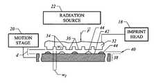
- FIG. 1depicts a lithographic system 10 in accordance with one embodiment of the present invention that includes a pair of spaced-apart bridge supports 12 having a bridge 14 and a stage support 16 extending therebetween. Bridge 14 and stage support 16 are spaced-apart. Coupled to bridge 14 is an imprint head 18 , which extends from bridge 14 toward stage support 16 and provides movement along the Z-axis. Disposed upon stage support 16 to face imprint head 18 is a motion stage, referred to as a substrate support stack 20 . Substrate support stack 20 is configured to move with respect to stage support 16 along X- and Y-axes.
- imprint head 18may provide movement along the X- and Y-axes, as well as the Z-axis
- motion stage 20may provide movement in the Z-axis, as well as the X- and Y-axes.
- An exemplary substrate support stack 20is disclosed in U.S. patent application Ser. No. 10/194,414, filed Jul. 11, 2002, entitled “Step and Repeat Imprint Lithography Systems,” assigned to the assignee of the present invention, and which is incorporated by reference herein in its entirety.
- a radiation source 22is coupled to lithographic system 10 to impinge actinic radiation upon substrate support stack 20 .
- radiation source 22is coupled to bridge 14 and includes a power generator 24 connected to radiation source 22 .
- Operation of lithographic system 10is typically controlled by a processor 26 that is in data communication therewith.
- a chuck 28to which a template 30 having a mold 32 thereon is mounted.
- An imprint head 18 and chuck 28is disclosed in U.S. patent application Ser. No. 10/293,224, entitled “A Chucking System for Modulating Shapes of Substrates” filed Nov. 13, 2002, which is assigned to the assignee of the present invention and incorporated by reference herein, as well as U.S. patent application Ser. No. 10/316,963, entitled “A Method for Modulating Shapes of Substrates” filed Dec. 11, 2002, which is assigned to the assignee of the present invention and incorporated by reference herein.
- Mold 32includes a plurality of features defined by a plurality of spaced-apart recessions 34 and protrusions 36 .
- the plurality of featuresdefines an original pattern that forms the basis of a pattern that is to be transferred into a wafer 38 positioned on motion stage 20 .
- imprint head 18 and/or motion stage 20may vary a distance “d” between mold 32 and wafer 38 .
- the features on mold 32may be imprinted into a flowable region of wafer 38 , discussed more fully below.
- Radiation source 22is located so that mold 32 is positioned between radiation source 22 and wafer 38 .
- mold 32is fabricated from a material that allows it to be substantially transparent to the radiation produced by radiation source 22 .
- a flowable regionsuch as an imprinting layer 40 , is disposed on a portion of a surface 42 that presents a substantially planar profile.
- a flowable regionmay be formed using any known technique, such as a hot embossing process disclosed in U.S. Pat. No. 5,772,905, which is incorporated by reference in its entirety herein, or a laser assisted direct imprinting (LADI) process of the type described by Chou et al. in Ultrafast and Direct Imprint of Nanostructures in Silicon, Nature , Col. 417, pp. 835-837, June 2002.
- LADIlaser assisted direct imprinting
- a flowable regionconsists of imprinting layer 40 being deposited as a plurality of spaced-apart discrete beads 44 of a material 46 on wafer 38 , discussed more fully below.
- An exemplary system for depositing beads 44is disclosed in U.S. patent application Ser. No. 10/191,749, filed Jul. 9, 2002, entitled “System and Method for Dispensing Liquids,” and which is assigned to the assignee of the present invention, and which is incorporated by reference in its entirety herein.
- Imprinting layer 40is formed from material 46 that may be selectively polymerized and cross-linked to record the original pattern therein, defining a recorded pattern.
- An exemplary composition for material 46is disclosed in U.S. patent application Ser. No.
- Material 46is shown in FIG. 4 as being crosslinked at points 48 , forming a cross-linked polymer material 50 .
- the pattern recorded in imprinting layer 40is produced, in part, by mechanical contact with mold 32 .
- distance “d”is reduced to allow imprinting beads 44 to come into mechanical contact with mold 32 , spreading beads 44 so as to form imprinting layer 40 with a contiguous formation of material 46 over surface 42 .
- distance “d”is reduced to allow sub-portions 52 of imprinting layer 40 to ingress into and fill recessions 34 .
- material 46is provided with the requisite properties to completely fill recessions 34 , while covering surface 42 with a contiguous formation of material 46 .
- sub-portions 54 of imprinting layer 40 in superimposition with protrusions 36remain after the desired, usually minimum, distance “d”, has been reached, leaving sub-portions 52 with a thickness t 1 , and sub-portions 54 with a thickness t 2 .
- Thicknesses “t 1 ” and “t 2 ”may be any thickness desired, dependent upon the application.
- radiation source 22produces actinic radiation that polymerizes and crosslinks material 46 , forming cross-linked polymer material 50 .
- the composition of imprinting layer 40transforms from material 46 to cross-linked polymer material 50 , which is a solid.
- crosslinked polymer material 50is solidified to provide side 56 of imprinting layer 40 with a shape conforming to a shape of a surface 58 of mold 32 , shown more clearly in FIG. 5 .
- imprint head 18shown in FIG. 2 , is moved to increase distance “d” so that mold 32 and imprinting layer 40 are spaced-apart.
- additional processingmay be employed to complete the patterning of wafer 38 .
- wafer 38 and imprinting layer 40may be etched to transfer the pattern of imprinting layer 40 into wafer 38 , providing a patterned surface 60 , shown in FIG. 6 .
- the material from which imprinting layer 40 is formedmay be varied to define a relative etch rate with respect to wafer 38 , as desired.
- the relative etch rate of imprinting layer 40 to wafer 38may be in a range of about 1.5:1 to about 100:1.
- the step-and-repeat processesincludes defining a plurality of regions, shown as, a- 1 , on wafer 38 in which the original pattern on mold 32 will be recorded.
- the original pattern on mold 32may be coextensive with the entire surface of mold 32 , or simply located to a sub-portion thereof.
- the present inventionwill be discussed with respect to the original pattern being coextensive with the surface of mold 32 that faces wafer 38 .
- Proper execution of a step-and-repeat processmay include proper alignment of mold 32 with each of regions a- 1 . To that end, mold 32 includes alignment marks (not shown).
- One or more of regions a- 1includes fiducial marks (not shown). By ensuring that alignment marks (not shown) are properly aligned with fiducial marks (not shown), proper alignment of mold 32 with one of regions a- 1 in superimposition therewith is ensured. To that end, sensing device 62 , discussed more fully below, may be employed. In this manner, mold 32 is sequentially contacted with each of processing regions a- 1 to record a pattern thereon.
- Sensing device 62may also be employed to facilitate process diagnostics.
- sensing device 62includes a light source 64 and an optical train 66 to focus light upon wafer 38 .
- Sensing device 62is configured to focus alignment radiation reflected from regions a- 1 onto a single focal plane, P, wherein an optical sensor 68 may be positioned.
- optical train 66may be configured to provide wavelength-dependent focal lengths, should it be desired and differing wavelengths of light employed.
- Lightmay be produced in any manner known in the art.
- a single broadband source of lightshown as a light 70 , may produce wavelengths that impinge upon optical train 66 .
- Optical band-pass filtersmay be disposed between the broadband source and the alignment marks (not shown).
- a plurality of sources of lightmay be employed, each one of which produces distinct wavelengths of light.
- Light 70is focused by optical train 66 to impinge upon regions a- 1 at one or more regions, shown as region R 1 and region R 2 .
- Region R 1 and region R 2Light reflects from regions R 1 and R 2 , shown as a reflected light 72 , and is collected by a collector lens 74 .
- Collector lens 74focuses all wavelengths of reflected light 72 onto plane P so that optical sensor 68 detects reflected light 72 .
- the reflected lightcontains information concerning characteristics of imprinting layer 40 using well known techniques. For example, characteristics, such as, film thickness, pattern quality, pattern alignment, pattern critical dimension variation and the like may be obtained by light sensed by sensor 68 .
- the information sensed by sensor 68is transmitted to processor 26 that quantizes the same to create measurement quantizations.
- Processor 26may then compare information received from sensor 68 to a priori information contained in a look up table, for example in memory 106 , to determine whether anomalies are present in imprinting layer 40 of regions a- 1 .
- the step-and-repeat imprinting processis found to facilitate determining a source of the anomaly. For example, were it found that a substantially similar anomaly was found in each of processing regions a- 1 , it could be deduced that imprint head 18 was the cause of the anomaly. To determine which subsystem of imprint head 18 contributed to, or caused, the anomaly, the subsystems could be systematically replaced.
- imprint head 18includes many subsystems, such as head housing 76 to which template 30 is coupled via a chucking system 80 that includes chuck body 28 .
- template 30includes opposed surfaces 84 and 86 and a periphery surface 88 extending therebetween.
- Surface 86faces chucking system 80
- mold 32extends from surface 84 .
- surface 58 of mold 32is spaced-apart from surface 84 of template 30 a distance on the order of micron, e.g., 15 microns.
- a calibration system 90is coupled to imprint head housing 76 , and chuck body 28 couples template 30 to calibration system 90 vis-à-vis a flexure system 92 .
- Calibration system 90facilitates proper orientation alignment between template 30 and wafer 38 , shown in FIG. 2 , thereby achieving a substantially uniform gap distance, “d”, therebetween.
- calibration system 90includes a plurality of actuators 94 , 96 and 98 and a base plate 100 .
- actuators 94 , 96 and 98are connected between housing 76 and base plate 100 .
- Flexure system 92includes flexure springs 102 and flexure ring 104 .
- Flexure ring 104is coupled between base plate 100 and flexure springs 102 .
- Motion of actuators 94 , 96 and 98orientates flexure ring 104 that may allow for a coarse calibration of flexure springs 102 and, therefore, chuck body 28 and template 30 .
- Actuators 94 , 96 and 98also facilitate translation of flexure ring 104 to the Z-axis.
- Flexure springs 102include a plurality of linear springs that facilitate gimbal-like motion in the X-Y plane so that proper orientation alignment may be achieved between wafer 38 and template 30 , shown in FIG. 2 .
- template 30would be replaced. Were the anomaly absent, then it could be concluded that mold 32 was the source of the anomaly. Were the anomaly still present, another subsystem of imprint head 18 could be replaced, such as, flexure springs 102 . Were the anomaly found to be absent in patterns of other regions a- 1 , and then it could be concluded that flexure springs 102 were the source. Were the anomaly still present, the other subsystems could be replaced, such as chuck body 28 , actuators 94 , 96 , and 98 , flexure ring 104 and the like.
- substrate support stack 20was the cause of the anomaly.
- the subsystems of substrate support stack 20may be individually replaced to identify the subsystem attributing to the anomaly.
- anomalies and their sourcesmay be determined without the use of Step-and-Repeat imprinting, e.g., with whole wafer patterning techniques.
- batches of substratesare examined during processing to determine whether anomalies are present on successive substrates. Were it found that a substantially similar anomaly was found in the same region, or a similar anomaly in differing regions, on successive wafers 38 , it could be deduced that mold 32 or chuck 28 was the cause of the defect. This could be verified by replacing mold 32 . Were the anomaly still present, it could be concluded that the cause of the anomaly was chuck 28 .
- the anomalycould be a film thickness variation.
- any one of a number of film thickness measurementscan be employed, such as ellipsometry, scatteromety, broad-band spectrometry and the like.
- An exemplary technique for measuring film thicknessis based on Fast Fourier Transform (FFT) of reflective radiation obtained from a broad-band spectrometer, which is disclosed in U.S. patent application Ser. No. 09/920,341 entitled “Methods For High-Precision Gap Orientation Sensing Between a Transparent Template and Substrate For Imprint Lithography”, which is incorporated by reference herein in its entirety.
- FFTFast Fourier Transform
- the techniquemay provide an average thickness of each thin film and its thickness variations by measuring at a predetermined number of sub-portions in one of processing regions a- 1 , e.g., 1,000 sub-portions.
- a predetermined number of sub-portions in one of processing regions a- 1e.g., 1,000 sub-portions.
- reflective radiationis digitized/quantized and a wave number obtained.
- the quantized datais then mapped into the frequency domain processing the same employing an FFT algorithm.
- p 1 and p 2are obtained, one of which may correspond to the film thickness at one of the sub-portions of one of processing regions a- 1 .
- the film thickness (t)may be a function of the frequency around which peak p 1 is centered. This may be derived or determined from a priori information.
- a mean valueis derived from these thickness measurements. Thereafter, each of the film thickness measurements are compared to the mean value. If any one of the thickness measurements vary from the mean more than a predetermined threshold it may be determined that an anomaly with respect to the film thickness measurement in associated processing region a- 1 is present. Furthermore, the location of the anomaly within the processing region may be ascertained.
- the actual value of the thresholdmay be any desired and is typically dependent upon several factors, such as the design tolerance of the pattern, the thickness of the film and the like. Alternatively, it has been found to determine anomalies as a variation from a standard deviation from the mean value.
- the standard deviationeither first, second, third standard deviation and the like, from the mean is compared with a predetermined threshold. From the foregoing the film thickness in each of the processing regions a- 1 may be determined, as well as whether a film thickness anomaly is present.
- a plurality of processing regionsis identified at step 200 .
- the characteristics of a subset of the plurality of processing regionsare measured.
- the subsetmay include all of the processing regions a- 1 .
- Determined, at step 204are a variation of one or more of the measured characteristics, using one or more of the measurement techniques mentioned above. In the present example, assume an anomaly was found in processing region b.
- a cause of the variation in processing region bis determined based upon a comparison with measured characteristics associated with processing regions a and c- 1 .
- processor 26is coupled to a memory 106 that stores code to be operated on by processor 26 .
- the codeincludes a first subroutine to control the sensing device 62 , shown in FIG. 8 , to impinge optical radiation on the plurality of processing regions a- 1 and detect optical radiation reflected therefrom.
- a second subroutineis included that controls the operations of the sensing device to obtain a predetermined number of measurements in the one of said plurality of processing regions a- 1 and quantizing the predetermined number of measurements to obtain a mean value, with the first subroutine determining the variation by comparing mean value with a predetermined threshold, which may be established as desired and/or based upon the application.
- the embodiments of the present invention described aboveare exemplary.
- the inventionhas been described with respect to measuring film thickness anomalies, other anomalies may be determined.
- distortions in the patternmay formed in imprinting layer may be sensed and the cause of the same determined employing the present invention.
- the systemmay be employed to detect anomalies in critical dimension variations of the pattern features, as well as, errors in field-to-field and/or layer-to-layer alignment. With such information adaptive control may be employed to correct/compensate for such anomalies.
- These measurementsmay be made either in-situ or post processes.
- the inventionhas been discussed with respect to being placed upon an imprint lithography machine. However, the invention may be performed by a separate machine and apart from the imprint lithography process.
Landscapes
- Engineering & Computer Science (AREA)
- Physics & Mathematics (AREA)
- General Physics & Mathematics (AREA)
- Chemical & Material Sciences (AREA)
- Nanotechnology (AREA)
- Manufacturing & Machinery (AREA)
- Microelectronics & Electronic Packaging (AREA)
- Crystallography & Structural Chemistry (AREA)
- Mathematical Physics (AREA)
- Biochemistry (AREA)
- Condensed Matter Physics & Semiconductors (AREA)
- Analytical Chemistry (AREA)
- Health & Medical Sciences (AREA)
- General Health & Medical Sciences (AREA)
- Immunology (AREA)
- Pathology (AREA)
- Life Sciences & Earth Sciences (AREA)
- Mechanical Engineering (AREA)
- Theoretical Computer Science (AREA)
- Computer Hardware Design (AREA)
- Power Engineering (AREA)
- Exposure Of Semiconductors, Excluding Electron Or Ion Beam Exposure (AREA)
- Shaping Of Tube Ends By Bending Or Straightening (AREA)
- Testing Or Measuring Of Semiconductors Or The Like (AREA)
- Length Measuring Devices By Optical Means (AREA)
Abstract
Description
- The field of invention relates generally to imprint lithography. More particularly, the present invention is directed measuring characteristics of a films patterned employing imprint lithography processes.
- Micro-fabrication involves the fabrication of very small structures, e.g., having features on the order of micro-meters or smaller. One area in which micro-fabrication has had a sizeable impact is in the processing of integrated circuits. As the semiconductor processing industry continues to strive for larger production yields while increasing the circuits per unit area formed on a substrate, micro-fabrication becomes increasingly important. Micro-fabrication provides greater process control while allowing increased reduction of the minimum feature dimension of the structures formed. Other areas of development in which micro-fabrication has been employed include biotechnology, optical technology, mechanical systems and the like.
- Exemplary micro-fabrication technique are disclosed in U.S. Pat. No. 6,334,960 to Willson et al. and by Chou et al. inUltrafast and Direct Imprint of Nanostructures in Silicon, Nature, Col. 417, pp. 835-837, June 2002, which is referred to as a laser assisted direct imprinting (LADI) process. Both of these processes involve the use of forming a layer on a substrate by embossing a flowable material with a mold and subsequently solidifying the flowable material to form a patterned layer.
- As a result of the small size of the features produced by micro-fabrication techniques, process diagnostics become increasingly important to determine the characteristics of films during processing and after processing. Many prior art process control and diagnostic techniques to facilitate determination of film characteristics have been employed in standard semiconductor processing operations. However, many of the existing process control and diagnostic techniques are not suitable for use with the embossing technique employed during micro-fabrication.
- Thus, a need exists for providing improved process and diagnostic techniques for use with micro-fabrication processes, such as imprint lithography.
- The present invention is directed to providing a method and system to measure characteristics of a film disposed on a substrate. The method includes identifying a plurality of processing regions on the film; measuring characteristics of a subset of the plurality of processing regions, defining measured characteristics; determining a variation of one of the measured characteristics; and associating a cause of the variations based upon a comparison of the one of the measured characteristics to measured characteristics associated with the remaining processing regions of the subset. The system carries out the aforementioned method. These and other embodiments are discussed more fully below.
FIG. 1 is a perspective view of a lithographic system in accordance with the present invention;FIG. 2 is a simplified elevation view of a lithographic system shown inFIG. 1 ;FIG. 3 is a simplified representation of material from which an imprinting layer, shown inFIG. 2 , is comprised before being polymerized and cross-linked;FIG. 4 is a simplified representation of cross-linked polymer material into which the material shown inFIG. 3 is transformed after being subjected to radiation;FIG. 5 is a simplified elevation view of a mold spaced-apart from the imprinting layer, shown inFIG. 1 , after patterning of the imprinting layer;FIG. 6 is a simplified elevation view of an additional imprinting layer positioned atop of the substrate, shown inFIG. 5 , after the pattern in the first imprinting layer is transferred therein;FIG. 7 is a top down view of the substrate shown inFIGS. 1 and 2 ;FIG. 8 is a plan view of a sensing system in accordance with the present invention;FIG. 9 is a detailed perspective view of an imprint head shown inFIG. 1 ;FIG. 10 is a detailed cross-sectional view of a substrate, having a mold thereon, attached to a chucking system, shown inFIG. 1 ;FIG. 11 is an exploded perspective view of the imprint head shown inFIG. 9 ;FIG. 12 is a graph showing the mapping of reflected radiation, sensed by the sensing system shown inFIG. 8 , in a frequency domain in accordance with the present invention; andFIG. 13 is a flow chart showing a process for measuring characteristics of a film in accordance with the present invention.FIG. 1 depicts alithographic system 10 in accordance with one embodiment of the present invention that includes a pair of spaced-apart bridge supports12 having abridge 14 and a stage support16 extending therebetween.Bridge 14 and stage support16 are spaced-apart. Coupled tobridge 14 is animprint head 18, which extends frombridge 14 toward stage support16 and provides movement along the Z-axis. Disposed upon stage support16 to faceimprint head 18 is a motion stage, referred to as asubstrate support stack 20.Substrate support stack 20 is configured to move with respect to stage support16 along X- and Y-axes. It should be understood thatimprint head 18 may provide movement along the X- and Y-axes, as well as the Z-axis, andmotion stage 20 may provide movement in the Z-axis, as well as the X- and Y-axes. An exemplarysubstrate support stack 20 is disclosed in U.S. patent application Ser. No. 10/194,414, filed Jul. 11, 2002, entitled “Step and Repeat Imprint Lithography Systems,” assigned to the assignee of the present invention, and which is incorporated by reference herein in its entirety. Aradiation source 22 is coupled tolithographic system 10 to impinge actinic radiation uponsubstrate support stack 20. As shown,radiation source 22 is coupled tobridge 14 and includes apower generator 24 connected toradiation source 22. Operation oflithographic system 10 is typically controlled by aprocessor 26 that is in data communication therewith.- Referring to both
FIGS. 1 and 2 , included inimprint head 18, is achuck 28 to which atemplate 30 having amold 32 thereon is mounted. Animprint head 18 andchuck 28 is disclosed in U.S. patent application Ser. No. 10/293,224, entitled “A Chucking System for Modulating Shapes of Substrates” filed Nov. 13, 2002, which is assigned to the assignee of the present invention and incorporated by reference herein, as well as U.S. patent application Ser. No. 10/316,963, entitled “A Method for Modulating Shapes of Substrates” filed Dec. 11, 2002, which is assigned to the assignee of the present invention and incorporated by reference herein. Mold32 includes a plurality of features defined by a plurality of spaced-apart recessions 34 andprotrusions 36. The plurality of features defines an original pattern that forms the basis of a pattern that is to be transferred into awafer 38 positioned onmotion stage 20. To that end,imprint head 18 and/ormotion stage 20 may vary a distance “d” betweenmold 32 andwafer 38. In this manner, the features onmold 32 may be imprinted into a flowable region ofwafer 38, discussed more fully below.Radiation source 22 is located so thatmold 32 is positioned betweenradiation source 22 andwafer 38. As a result,mold 32 is fabricated from a material that allows it to be substantially transparent to the radiation produced byradiation source 22. - Referring to both
FIGS. 2 and 3 , a flowable region, such as animprinting layer 40, is disposed on a portion of asurface 42 that presents a substantially planar profile. A flowable region may be formed using any known technique, such as a hot embossing process disclosed in U.S. Pat. No. 5,772,905, which is incorporated by reference in its entirety herein, or a laser assisted direct imprinting (LADI) process of the type described by Chou et al. inUltrafast and Direct Imprint of Nanostructures in Silicon, Nature, Col. 417, pp. 835-837, June 2002. In the present embodiment, however, a flowable region consists ofimprinting layer 40 being deposited as a plurality of spaced-apartdiscrete beads 44 of amaterial 46 onwafer 38, discussed more fully below. An exemplary system for depositingbeads 44 is disclosed in U.S. patent application Ser. No. 10/191,749, filed Jul. 9, 2002, entitled “System and Method for Dispensing Liquids,” and which is assigned to the assignee of the present invention, and which is incorporated by reference in its entirety herein.Imprinting layer 40 is formed frommaterial 46 that may be selectively polymerized and cross-linked to record the original pattern therein, defining a recorded pattern. An exemplary composition formaterial 46 is disclosed in U.S. patent application Ser. No. 10/463,396, filed Jun. 16, 2003 and entitled “Method to Reduce Adhesion Between a Conformable Region and a Pattern of a Mold,” which is incorporated by reference in its entirety herein.Material 46 is shown inFIG. 4 as being crosslinked atpoints 48, forming across-linked polymer material 50. - Referring to
FIGS. 2, 3 and5, the pattern recorded inimprinting layer 40 is produced, in part, by mechanical contact withmold 32. To that end, distance “d” is reduced to allowimprinting beads 44 to come into mechanical contact withmold 32, spreadingbeads 44 so as to form imprintinglayer 40 with a contiguous formation ofmaterial 46 oversurface 42. In one embodiment, distance “d” is reduced to allowsub-portions 52 ofimprinting layer 40 to ingress into and fillrecessions 34. - To facilitate filling of
recessions 34,material 46 is provided with the requisite properties to completely fillrecessions 34, while coveringsurface 42 with a contiguous formation ofmaterial 46. In the present embodiment, sub-portions54 ofimprinting layer 40 in superimposition withprotrusions 36 remain after the desired, usually minimum, distance “d”, has been reached, leaving sub-portions52 with a thickness t1, and sub-portions54 with a thickness t2. Thicknesses “t1” and “t2” may be any thickness desired, dependent upon the application. - Referring to
FIGS. 2, 3 and4, after a desired distance “d” has been reached,radiation source 22 produces actinic radiation that polymerizes andcrosslinks material 46, formingcross-linked polymer material 50. As a result, the composition ofimprinting layer 40 transforms frommaterial 46 tocross-linked polymer material 50, which is a solid. Specifically,crosslinked polymer material 50 is solidified to provideside 56 ofimprinting layer 40 with a shape conforming to a shape of asurface 58 ofmold 32, shown more clearly inFIG. 5 . After imprintinglayer 40 is transformed to consist ofcross-linked polymer material 50, shown inFIG. 4 ,imprint head 18, shown inFIG. 2 , is moved to increase distance “d” so thatmold 32 andimprinting layer 40 are spaced-apart. - Referring to
FIG. 5 , additional processing may be employed to complete the patterning ofwafer 38. For example,wafer 38 andimprinting layer 40 may be etched to transfer the pattern ofimprinting layer 40 intowafer 38, providing a patternedsurface 60, shown inFIG. 6 . To facilitate etching, the material from whichimprinting layer 40 is formed may be varied to define a relative etch rate with respect towafer 38, as desired. The relative etch rate ofimprinting layer 40 towafer 38 may be in a range of about 1.5:1 to about 100:1. - Referring to
FIGS. 7 and 8 , typically theentire wafer 38 is patterned employing a step-and-repeat process. The step-and-repeat processes includes defining a plurality of regions, shown as, a-1, onwafer 38 in which the original pattern onmold 32 will be recorded. The original pattern onmold 32 may be coextensive with the entire surface ofmold 32, or simply located to a sub-portion thereof. The present invention will be discussed with respect to the original pattern being coextensive with the surface ofmold 32 that faceswafer 38. Proper execution of a step-and-repeat process may include proper alignment ofmold 32 with each of regions a-1. To that end,mold 32 includes alignment marks (not shown). One or more of regions a-1 includes fiducial marks (not shown). By ensuring that alignment marks (not shown) are properly aligned with fiducial marks (not shown), proper alignment ofmold 32 with one of regions a-1 in superimposition therewith is ensured. To that end,sensing device 62, discussed more fully below, may be employed. In this manner,mold 32 is sequentially contacted with each of processing regions a-1 to record a pattern thereon. Sensing device 62 may also be employed to facilitate process diagnostics. To that end,sensing device 62 includes alight source 64 and anoptical train 66 to focus light uponwafer 38.Sensing device 62 is configured to focus alignment radiation reflected from regions a-1 onto a single focal plane, P, wherein anoptical sensor 68 may be positioned. As a result,optical train 66 may be configured to provide wavelength-dependent focal lengths, should it be desired and differing wavelengths of light employed. Light may be produced in any manner known in the art. For example, a single broadband source of light, shown as a light70, may produce wavelengths that impinge uponoptical train 66. Optical band-pass filters (not shown) may be disposed between the broadband source and the alignment marks (not shown).- Alternatively, a plurality of sources of light (not shown) may be employed, each one of which produces distinct wavelengths of light.
Light 70 is focused byoptical train 66 to impinge upon regions a-1 at one or more regions, shown as region R1and region R2. Light reflects from regions R1and R2, shown as a reflectedlight 72, and is collected by acollector lens 74.Collector lens 74 focuses all wavelengths of reflected light72 onto plane P so thatoptical sensor 68 detects reflectedlight 72. The reflected light contains information concerning characteristics ofimprinting layer 40 using well known techniques. For example, characteristics, such as, film thickness, pattern quality, pattern alignment, pattern critical dimension variation and the like may be obtained by light sensed bysensor 68. The information sensed bysensor 68 is transmitted toprocessor 26 that quantizes the same to create measurement quantizations.Processor 26 may then compare information received fromsensor 68 to a priori information contained in a look up table, for example inmemory 106, to determine whether anomalies are present inimprinting layer 40 of regions a-1. - Referring to
FIGS. 1 and 7 , were an anomaly found in the pattern generated in a processing region a-1, the step-and-repeat imprinting process is found to facilitate determining a source of the anomaly. For example, were it found that a substantially similar anomaly was found in each of processing regions a-1, it could be deduced thatimprint head 18 was the cause of the anomaly. To determine which subsystem ofimprint head 18 contributed to, or caused, the anomaly, the subsystems could be systematically replaced. - For example, referring to
FIGS. 9 and 10 ,imprint head 18 includes many subsystems, such ashead housing 76 to whichtemplate 30 is coupled via a chucking system80 that includeschuck body 28. Specifically,template 30 includes opposedsurfaces periphery surface 88 extending therebetween.Surface 86 faces chucking system80, andmold 32 extends fromsurface 84. To ensure that fluid frombeads 44, shown inFIG. 2 , do not spread beyond the area ofmold 32,surface 58 ofmold 32 is spaced-apart fromsurface 84 of template30 a distance on the order of micron, e.g., 15 microns. Acalibration system 90 is coupled toimprint head housing 76, and chuckbody 28couples template 30 tocalibration system 90 vis-à-vis aflexure system 92.Calibration system 90 facilitates proper orientation alignment betweentemplate 30 andwafer 38, shown inFIG. 2 , thereby achieving a substantially uniform gap distance, “d”, therebetween. - Referring to both
FIGS. 9 and 11 ,calibration system 90 includes a plurality ofactuators base plate 100. Specifically, actuators94,96 and98 are connected betweenhousing 76 andbase plate 100.Flexure system 92 includes flexure springs102 andflexure ring 104.Flexure ring 104 is coupled betweenbase plate 100 and flexure springs102. Motion ofactuators flexure ring 104 that may allow for a coarse calibration of flexure springs102 and, therefore, chuckbody 28 andtemplate 30.Actuators flexure ring 104 to the Z-axis. Flexure springs102 include a plurality of linear springs that facilitate gimbal-like motion in the X-Y plane so that proper orientation alignment may be achieved betweenwafer 38 andtemplate 30, shown inFIG. 2 . - Referring to
FIGS. 1, 10 and11, to determine whethermold 32 attributed to an anomaly,template 30 would be replaced. Were the anomaly absent, then it could be concluded thatmold 32 was the source of the anomaly. Were the anomaly still present, another subsystem ofimprint head 18 could be replaced, such as, flexure springs102. Were the anomaly found to be absent in patterns of other regions a-1, and then it could be concluded that flexure springs102 were the source. Were the anomaly still present, the other subsystems could be replaced, such aschuck body 28,actuators flexure ring 104 and the like. - Were it observed that the anomaly appeared in only one of processing regions, then it could be deduced that
substrate support stack 20 was the cause of the anomaly. As discussed above with respect toimprint head 18, the subsystems ofsubstrate support stack 20 may be individually replaced to identify the subsystem attributing to the anomaly. - It should also be understood, however, that anomalies and their sources may be determined without the use of Step-and-Repeat imprinting, e.g., with whole wafer patterning techniques. To that end, batches of substrates are examined during processing to determine whether anomalies are present on successive substrates. Were it found that a substantially similar anomaly was found in the same region, or a similar anomaly in differing regions, on
successive wafers 38, it could be deduced thatmold 32 orchuck 28 was the cause of the defect. This could be verified by replacingmold 32. Were the anomaly still present, it could be concluded that the cause of the anomaly waschuck 28. Were the anomaly found not to repeat upon replacement ofmold 32, it could be concluded thatmold 32 was the cause of the anomaly. Were it observed that the anomaly appeared on a limited number or one ofwafers 38, then it could be deduced thatwafer 38 was the cause of the anomaly. - For example, the anomaly could be a film thickness variation. To that end, any one of a number of film thickness measurements can be employed, such as ellipsometry, scatteromety, broad-band spectrometry and the like. An exemplary technique for measuring film thickness is based on Fast Fourier Transform (FFT) of reflective radiation obtained from a broad-band spectrometer, which is disclosed in U.S. patent application Ser. No. 09/920,341 entitled “Methods For High-Precision Gap Orientation Sensing Between a Transparent Template and Substrate For Imprint Lithography”, which is incorporated by reference herein in its entirety. For multi-layer films, the technique may provide an average thickness of each thin film and its thickness variations by measuring at a predetermined number of sub-portions in one of processing regions a-1, e.g., 1,000 sub-portions. Employing FFT thickness measurement techniques, reflective radiation is digitized/quantized and a wave number obtained. The quantized data is then mapped into the frequency domain processing the same employing an FFT algorithm. In the frequency domain, one or more peaks, shown in
FIG. 12 as p1and p2, are obtained, one of which may correspond to the film thickness at one of the sub-portions of one of processing regions a-1. For a clearly defined single peak, for example, p1, the film thickness (t) may be a function of the frequency around which peak p1is centered. This may be derived or determined from a priori information. - For example, after obtaining film thickness measurements at several or all of the sub-portions, a mean value is derived from these thickness measurements. Thereafter, each of the film thickness measurements are compared to the mean value. If any one of the thickness measurements vary from the mean more than a predetermined threshold it may be determined that an anomaly with respect to the film thickness measurement in associated processing region a-1 is present. Furthermore, the location of the anomaly within the processing region may be ascertained. The actual value of the threshold may be any desired and is typically dependent upon several factors, such as the design tolerance of the pattern, the thickness of the film and the like. Alternatively, it has been found to determine anomalies as a variation from a standard deviation from the mean value. To that end, the standard deviation, either first, second, third standard deviation and the like, from the mean is compared with a predetermined threshold. From the foregoing the film thickness in each of the processing regions a-1 may be determined, as well as whether a film thickness anomaly is present.
- Referring to
FIGS. 1 and 13 , in operation, a plurality of processing regions is identified atstep 200. At step202 the characteristics of a subset of the plurality of processing regions are measured. The subset may include all of the processing regions a-1. Determined, atstep 204 are a variation of one or more of the measured characteristics, using one or more of the measurement techniques mentioned above. In the present example, assume an anomaly was found in processing region b. Atstep 206, a cause of the variation in processing region b is determined based upon a comparison with measured characteristics associated with processing regions a and c-1. To facilitate the aforementioned operation,processor 26 is coupled to amemory 106 that stores code to be operated on byprocessor 26. The code includes a first subroutine to control thesensing device 62, shown inFIG. 8 , to impinge optical radiation on the plurality of processing regions a-1 and detect optical radiation reflected therefrom. A second subroutine is included that controls the operations of the sensing device to obtain a predetermined number of measurements in the one of said plurality of processing regions a-1 and quantizing the predetermined number of measurements to obtain a mean value, with the first subroutine determining the variation by comparing mean value with a predetermined threshold, which may be established as desired and/or based upon the application. - The embodiments of the present invention described above are exemplary. Although the invention has been described with respect to measuring film thickness anomalies, other anomalies may be determined. For example, distortions in the pattern may formed in imprinting layer may be sensed and the cause of the same determined employing the present invention. As a result, the system may be employed to detect anomalies in critical dimension variations of the pattern features, as well as, errors in field-to-field and/or layer-to-layer alignment. With such information adaptive control may be employed to correct/compensate for such anomalies. These measurements may be made either in-situ or post processes. Furthermore, the invention has been discussed with respect to being placed upon an imprint lithography machine. However, the invention may be performed by a separate machine and apart from the imprint lithography process.
- As a result, many changes and modifications may be made to the disclosure recited above, while remaining within the scope of the invention. Therefore, the scope of the invention should not be limited by the above description, but instead should be determined with reference to the appended claims along with their full scope of equivalents.
Claims (28)
Priority Applications (8)
| Application Number | Priority Date | Filing Date | Title |
|---|---|---|---|
| US10/782,187US7019835B2 (en) | 2004-02-19 | 2004-02-19 | Method and system to measure characteristics of a film disposed on a substrate |
| CNB2005800048230ACN100498209C (en) | 2004-02-19 | 2005-02-14 | Method and system to measure characteristics of a film disposed on a substrate |
| PCT/US2005/004414WO2005079304A2 (en) | 2004-02-19 | 2005-02-14 | Method and system to measure characteristics of a film disposed on a substrate |
| JP2006554141AJP2007523492A (en) | 2004-02-19 | 2005-02-14 | Method and system for measuring properties of a film placed on a substrate |
| EP05722971AEP1721120A4 (en) | 2004-02-19 | 2005-02-14 | Method and system to measure characteristics of a film disposed on a substrate |
| KR1020067013994AKR101076028B1 (en) | 2004-02-19 | 2005-02-14 | Method and system to measure characteristics of a film disposed on a substrate |
| MYPI20050599AMY134681A (en) | 2004-02-19 | 2005-02-17 | Method and system to measure characteristics of a film disposed on a substrate |
| TW094104847ATWI250276B (en) | 2004-02-19 | 2005-02-18 | Method and system to measure characteristics of a film disposed on a substrate |
Applications Claiming Priority (1)
| Application Number | Priority Date | Filing Date | Title |
|---|---|---|---|
| US10/782,187US7019835B2 (en) | 2004-02-19 | 2004-02-19 | Method and system to measure characteristics of a film disposed on a substrate |
Publications (2)
| Publication Number | Publication Date |
|---|---|
| US20050185169A1true US20050185169A1 (en) | 2005-08-25 |
| US7019835B2 US7019835B2 (en) | 2006-03-28 |
Family
ID=34860994
Family Applications (1)
| Application Number | Title | Priority Date | Filing Date |
|---|---|---|---|
| US10/782,187Expired - LifetimeUS7019835B2 (en) | 2004-02-19 | 2004-02-19 | Method and system to measure characteristics of a film disposed on a substrate |
Country Status (8)
| Country | Link |
|---|---|
| US (1) | US7019835B2 (en) |
| EP (1) | EP1721120A4 (en) |
| JP (1) | JP2007523492A (en) |
| KR (1) | KR101076028B1 (en) |
| CN (1) | CN100498209C (en) |
| MY (1) | MY134681A (en) |
| TW (1) | TWI250276B (en) |
| WO (1) | WO2005079304A2 (en) |
Cited By (7)
| Publication number | Priority date | Publication date | Assignee | Title |
|---|---|---|---|---|
| US20070266875A1 (en)* | 2004-08-10 | 2007-11-22 | Asml Netherlands B.V. | Imprint Lithographic Apparatus, Device Manufacturing Method and Device Manufactured Thereby |
| WO2007142250A1 (en) | 2006-05-31 | 2007-12-13 | Canon Kabushiki Kaisha | Gap measuring method, imprint method, and imprint apparatus |
| US20080160129A1 (en)* | 2006-05-11 | 2008-07-03 | Molecular Imprints, Inc. | Template Having a Varying Thickness to Facilitate Expelling a Gas Positioned Between a Substrate and the Template |
| EP2184577A1 (en)* | 2008-11-08 | 2010-05-12 | Horiba, Ltd. | Optical measurement apparatus, spectroscopic ellipsometer, recording medium, and measurement method |
| US20110198769A1 (en)* | 2010-02-17 | 2011-08-18 | Canon Kabushiki Kaisha | Imprint apparatus and article manufacturing method |
| US8287792B2 (en) | 2009-01-29 | 2012-10-16 | Samsung Electronics Co., Ltd. | Methods of forming fine patterns using a nanoimprint lithography |
| US11164302B2 (en) | 2019-08-08 | 2021-11-02 | Canon Kabushiki Kaisha | Systems and methods for classifying images of an imprinted film |
Families Citing this family (17)
| Publication number | Priority date | Publication date | Assignee | Title |
|---|---|---|---|---|
| US20070228593A1 (en)* | 2006-04-03 | 2007-10-04 | Molecular Imprints, Inc. | Residual Layer Thickness Measurement and Correction |
| JP4878264B2 (en)* | 2006-11-02 | 2012-02-15 | キヤノン株式会社 | Inspection method, inspection apparatus, and imprint apparatus |
| US20100112220A1 (en)* | 2008-11-03 | 2010-05-06 | Molecular Imprints, Inc. | Dispense system set-up and characterization |
| WO2010111307A1 (en)* | 2009-03-23 | 2010-09-30 | Intevac, Inc. | A process for optimization of island to trench ratio in patterned media |
| JP5173944B2 (en)* | 2009-06-16 | 2013-04-03 | キヤノン株式会社 | Imprint apparatus and article manufacturing method |
| JP2011009250A (en)* | 2009-06-23 | 2011-01-13 | Toshiba Corp | Substrate processing method, method of manufacturing semiconductor device and imprint device |
| NL2004949A (en)* | 2009-08-21 | 2011-02-22 | Asml Netherlands Bv | Inspection method and apparatus. |
| JP2011053013A (en)* | 2009-08-31 | 2011-03-17 | Nof Corp | Method of inspecting nanoimprint molding laminate |
| JP5024464B2 (en)* | 2011-01-31 | 2012-09-12 | 株式会社日立製作所 | Pattern forming method and mold |
| JP5548151B2 (en)* | 2011-02-17 | 2014-07-16 | 株式会社日立ハイテクノロジーズ | Pattern shape inspection method and apparatus |
| EP2718465B1 (en) | 2011-06-09 | 2022-04-13 | Illumina, Inc. | Method of making an analyte array |
| CA2856163C (en) | 2011-10-28 | 2019-05-07 | Illumina, Inc. | Microarray fabrication system and method |
| JP6221461B2 (en)* | 2013-07-25 | 2017-11-01 | 大日本印刷株式会社 | Defect analysis method, uneven pattern structure manufacturing method, and imprint system |
| JP2014064022A (en)* | 2013-11-11 | 2014-04-10 | Canon Inc | Imprint device |
| JP5933060B2 (en)* | 2015-03-13 | 2016-06-08 | キヤノン株式会社 | Imprint apparatus and method, and article manufacturing method |
| US10886155B2 (en)* | 2019-01-16 | 2021-01-05 | Applied Materials, Inc. | Optical stack deposition and on-board metrology |
| US12326376B1 (en)* | 2022-12-21 | 2025-06-10 | Hrl Laboratories, Llc | Spike arrays for small displacement force measurement |
Citations (58)
| Publication number | Priority date | Publication date | Assignee | Title |
|---|---|---|---|---|
| US4444801A (en)* | 1981-01-14 | 1984-04-24 | Hitachi, Ltd. | Method and apparatus for correcting transparent defects on a photomask |
| US4512848A (en)* | 1984-02-06 | 1985-04-23 | Exxon Research And Engineering Co. | Procedure for fabrication of microstructures over large areas using physical replication |
| US4722878A (en)* | 1984-11-09 | 1988-02-02 | Mitsubishi Denki Kabushiki Kaisha | Photomask material |
| US4731155A (en)* | 1987-04-15 | 1988-03-15 | General Electric Company | Process for forming a lithographic mask |
| US5028366A (en)* | 1988-01-12 | 1991-07-02 | Air Products And Chemicals, Inc. | Water based mold release compositions for making molded polyurethane foam |
| US5235400A (en)* | 1988-10-12 | 1993-08-10 | Hitachi, Ltd. | Method of and apparatus for detecting defect on photomask |
| US5331407A (en)* | 1991-03-04 | 1994-07-19 | Hitachi, Ltd. | Method and apparatus for detecting a circuit pattern |
| US5425848A (en)* | 1993-03-16 | 1995-06-20 | U.S. Philips Corporation | Method of providing a patterned relief of cured photoresist on a flat substrate surface and device for carrying out such a method |
| US5563702A (en)* | 1991-08-22 | 1996-10-08 | Kla Instruments Corporation | Automated photomask inspection apparatus and method |
| US5601641A (en)* | 1992-07-21 | 1997-02-11 | Tse Industries, Inc. | Mold release composition with polybutadiene and method of coating a mold core |
| US5625193A (en)* | 1995-07-10 | 1997-04-29 | Qc Optics, Inc. | Optical inspection system and method for detecting flaws on a diffractive surface |
| US5669303A (en)* | 1996-03-04 | 1997-09-23 | Motorola | Apparatus and method for stamping a surface |
| US5772905A (en)* | 1995-11-15 | 1998-06-30 | Regents Of The University Of Minnesota | Nanoimprint lithography |
| US5774574A (en)* | 1994-11-30 | 1998-06-30 | Dainippon Screen Mfg. Co., Ltd. | Pattern defect detection apparatus |
| US5837892A (en)* | 1996-10-25 | 1998-11-17 | Camelot Systems, Inc. | Method and apparatus for measuring the size of drops of a viscous material dispensed from a dispensing system |
| US5849209A (en)* | 1995-03-31 | 1998-12-15 | Johnson & Johnson Vision Products, Inc. | Mold material made with additives |
| US5849222A (en)* | 1995-09-29 | 1998-12-15 | Johnson & Johnson Vision Products, Inc. | Method for reducing lens hole defects in production of contact lens blanks |
| US5916584A (en)* | 1994-10-25 | 1999-06-29 | Daratech Proprietary Limited | Controlled release container with core and outer shell |
| US6016696A (en)* | 1998-09-25 | 2000-01-25 | Lucent Technologies Inc. | Method for determining volume changes in viscous liquids |
| US6052183A (en)* | 1999-04-14 | 2000-04-18 | Winbond Electronics Corp | In-situ particle monitoring |
| US6112588A (en)* | 1996-10-25 | 2000-09-05 | Speedline Technologies, Inc. | Method and apparatus for measuring the size of drops of a viscous material dispensed from a dispensing system |
| US6133576A (en)* | 1996-07-22 | 2000-10-17 | Kla Instruments Corporation | Broad spectrum ultraviolet inspection methods employing catadioptric imaging |
| US6245581B1 (en)* | 2000-04-19 | 2001-06-12 | Advanced Micro Devices, Inc. | Method and apparatus for control of critical dimension using feedback etch control |
| US6278519B1 (en)* | 1998-01-29 | 2001-08-21 | Therma-Wave, Inc. | Apparatus for analyzing multi-layer thin film stacks on semiconductors |
| US6309580B1 (en)* | 1995-11-15 | 2001-10-30 | Regents Of The University Of Minnesota | Release surfaces, particularly for use in nanoimprint lithography |
| US6334960B1 (en)* | 1999-03-11 | 2002-01-01 | Board Of Regents, The University Of Texas System | Step and flash imprint lithography |
| US20020042027A1 (en)* | 1998-10-09 | 2002-04-11 | Chou Stephen Y. | Microscale patterning and articles formed thereby |
| US6387787B1 (en)* | 2001-03-02 | 2002-05-14 | Motorola, Inc. | Lithographic template and method of formation and use |
| US6391217B2 (en)* | 1999-12-23 | 2002-05-21 | University Of Massachusetts | Methods and apparatus for forming submicron patterns on films |
| US20020132482A1 (en)* | 2000-07-18 | 2002-09-19 | Chou Stephen Y. | Fluid pressure imprint lithography |
| US6517995B1 (en)* | 1999-09-14 | 2003-02-11 | Massachusetts Institute Of Technology | Fabrication of finely featured devices by liquid embossing |
| US6518189B1 (en)* | 1995-11-15 | 2003-02-11 | Regents Of The University Of Minnesota | Method and apparatus for high density nanostructures |
| US20030080471A1 (en)* | 2001-10-29 | 2003-05-01 | Chou Stephen Y. | Lithographic method for molding pattern with nanoscale features |
| US6561706B2 (en)* | 2001-06-28 | 2003-05-13 | Advanced Micro Devices, Inc. | Critical dimension monitoring from latent image |
| US6603538B1 (en)* | 2000-11-21 | 2003-08-05 | Applied Materials, Inc. | Method and apparatus employing optical emission spectroscopy to detect a fault in process conditions of a semiconductor processing system |
| US6633391B1 (en)* | 2000-11-07 | 2003-10-14 | Applied Materials, Inc | Monitoring of film characteristics during plasma-based semi-conductor processing using optical emission spectroscopy |
| US20030205658A1 (en)* | 2002-05-01 | 2003-11-06 | Molecular Imprints, Inc. | Methods of inspecting a lithography template |
| US6646626B1 (en)* | 1999-11-01 | 2003-11-11 | Motorola, Inc. | Method and apparatus for automatic viewing angle adjustment for liquid crystal display |
| US20040008334A1 (en)* | 2002-07-11 | 2004-01-15 | Sreenivasan Sidlgata V. | Step and repeat imprint lithography systems |
| US20040009673A1 (en)* | 2002-07-11 | 2004-01-15 | Sreenivasan Sidlgata V. | Method and system for imprint lithography using an electric field |
| US20040007799A1 (en)* | 2002-07-11 | 2004-01-15 | Choi Byung Jin | Formation of discontinuous films during an imprint lithography process |
| US20040021254A1 (en)* | 2002-08-01 | 2004-02-05 | Sreenivasan Sidlgata V. | Alignment methods for imprint lithography |
| US20040021866A1 (en)* | 2002-08-01 | 2004-02-05 | Watts Michael P.C. | Scatterometry alignment for imprint lithography |
| US20040022888A1 (en)* | 2002-08-01 | 2004-02-05 | Sreenivasan Sidlgata V. | Alignment systems for imprint lithography |
| US6696220B2 (en)* | 2000-10-12 | 2004-02-24 | Board Of Regents, The University Of Texas System | Template for room temperature, low pressure micro-and nano-imprint lithography |
| US20040036201A1 (en)* | 2000-07-18 | 2004-02-26 | Princeton University | Methods and apparatus of field-induced pressure imprint lithography |
| US20040046288A1 (en)* | 2000-07-18 | 2004-03-11 | Chou Stephen Y. | Laset assisted direct imprint lithography |
| US6746319B2 (en)* | 2001-08-10 | 2004-06-08 | Ebara Corporation | Measuring apparatus |
| US20040110856A1 (en)* | 2002-12-04 | 2004-06-10 | Young Jung Gun | Polymer solution for nanoimprint lithography to reduce imprint temperature and pressure |
| US20040112153A1 (en)* | 2002-12-12 | 2004-06-17 | Molecular Imprints, Inc. | Method and system for determining characteristics of substrates employing fluid geometries |
| US20040137734A1 (en)* | 1995-11-15 | 2004-07-15 | Princeton University | Compositions and processes for nanoimprinting |
| US6771374B1 (en)* | 2002-01-16 | 2004-08-03 | Advanced Micro Devices, Inc. | Scatterometry based measurements of a rotating substrate |
| US20040156108A1 (en)* | 2001-10-29 | 2004-08-12 | Chou Stephen Y. | Articles comprising nanoscale patterns with reduced edge roughness and methods of making same |
| US6776094B1 (en)* | 1993-10-04 | 2004-08-17 | President & Fellows Of Harvard College | Kit For Microcontact Printing |
| US20040192041A1 (en)* | 2003-03-27 | 2004-09-30 | Jun-Ho Jeong | UV nanoimprint lithography process using elementwise embossed stamp and selectively additive pressurization |
| US20040197843A1 (en)* | 2001-07-25 | 2004-10-07 | Chou Stephen Y. | Nanochannel arrays and their preparation and use for high throughput macromolecular analysis |
| US20040250945A1 (en)* | 2003-06-10 | 2004-12-16 | Industrial Technology Research Institute | Method for and apparatus for bonding patterned imprint to a substrate by adhering means |
| US20050037143A1 (en)* | 2000-07-18 | 2005-02-17 | Chou Stephen Y. | Imprint lithography with improved monitoring and control and apparatus therefor |
Family Cites Families (30)
| Publication number | Priority date | Publication date | Assignee | Title |
|---|---|---|---|---|
| JPS57118246A (en)* | 1981-01-14 | 1982-07-23 | Hitachi Ltd | Method and device for correcting white spot defect of photomask |
| JPH0215612A (en)* | 1988-07-04 | 1990-01-19 | Oki Electric Ind Co Ltd | Formation of identification code of semiconductor device |
| JPH0224848A (en) | 1988-07-14 | 1990-01-26 | Canon Inc | Production of substrate for optical recording medium |
| JPH0292603A (en) | 1988-09-30 | 1990-04-03 | Hoya Corp | Manufacture of data recording board with guide groove |
| JPH08124977A (en)* | 1994-10-19 | 1996-05-17 | Hitachi Ltd | Semiconductor device failure analysis system |
| US5923430A (en)* | 1993-06-17 | 1999-07-13 | Ultrapointe Corporation | Method for characterizing defects on semiconductor wafers |
| JPH10209230A (en)* | 1997-01-23 | 1998-08-07 | Hitachi Ltd | Failure analysis apparatus and method |
| AU3818997A (en) | 1997-07-25 | 1999-02-16 | Regents Of The University Of Minnesota | Single-electron floating-gate mos memory |
| JP3780700B2 (en) | 1998-05-26 | 2006-05-31 | セイコーエプソン株式会社 | Pattern forming method, pattern forming apparatus, pattern forming plate, pattern forming plate manufacturing method, color filter manufacturing method, conductive film manufacturing method, and liquid crystal panel manufacturing method |
| WO2000021689A1 (en) | 1998-10-09 | 2000-04-20 | The Trustees Of Princeton University | Microscale patterning and articles formed thereby |
| US6466895B1 (en)* | 1999-07-16 | 2002-10-15 | Applied Materials, Inc. | Defect reference system automatic pattern classification |
| JP4274649B2 (en)* | 1999-10-07 | 2009-06-10 | 株式会社日立製作所 | Fine pattern inspection method and apparatus |
| SE515962C2 (en)* | 2000-03-15 | 2001-11-05 | Obducat Ab | Device for transferring patterns to objects |
| JP2001338870A (en)* | 2000-03-24 | 2001-12-07 | Nikon Corp | Scanning exposure apparatus and method, management apparatus and method, and device manufacturing method |
| US7635262B2 (en) | 2000-07-18 | 2009-12-22 | Princeton University | Lithographic apparatus for fluid pressure imprint lithography |
| JP2004505273A (en)* | 2000-08-01 | 2004-02-19 | ボード・オブ・リージエンツ,ザ・ユニバーシテイ・オブ・テキサス・システム | Method for highly accurate sensing of gap and orientation between transparent template and substrate for transfer lithography |
| US7317531B2 (en)* | 2002-12-05 | 2008-01-08 | Kla-Tencor Technologies Corporation | Apparatus and methods for detecting overlay errors using scatterometry |
| US6633831B2 (en)* | 2000-09-20 | 2003-10-14 | Kla Tencor Technologies | Methods and systems for determining a critical dimension and a thin film characteristic of a specimen |
| US6836560B2 (en)* | 2000-11-13 | 2004-12-28 | Kla - Tencor Technologies Corporation | Advanced phase shift inspection method |
| JP4170611B2 (en)* | 2001-03-29 | 2008-10-22 | 株式会社東芝 | Defect detection method and defect detection apparatus for semiconductor integrated circuit |
| JP2003100599A (en)* | 2001-09-25 | 2003-04-04 | Nikon Corp | Exposure apparatus adjustment method and exposure system |
| JP3641229B2 (en) | 2001-09-27 | 2005-04-20 | 株式会社東芝 | Sample inspection apparatus and sample inspection method |
| AU2003230676A1 (en) | 2002-03-15 | 2003-09-29 | Princeton University | Laser assisted direct imprint lithography |
| CN1678443B (en) | 2002-05-24 | 2012-12-19 | 斯蒂文·Y·周 | Method and apparatus for field pressure-sensitive imprint lithography |
| WO2004005419A1 (en)* | 2002-07-03 | 2004-01-15 | The Lubrizol Corporation | Rheology control for_adhesives based on formaldehyde resins |
| MY164487A (en)* | 2002-07-11 | 2017-12-29 | Molecular Imprints Inc | Step and repeat imprint lithography processes |
| US7077992B2 (en) | 2002-07-11 | 2006-07-18 | Molecular Imprints, Inc. | Step and repeat imprint lithography processes |
| WO2004044651A1 (en)* | 2002-11-13 | 2004-05-27 | Molecular Imprints, Inc. | A chucking system and method for modulating shapes of substrates |
| WO2004053426A1 (en)* | 2002-12-05 | 2004-06-24 | Kla-Tencor Technologies Corporation | Apparatus and methods for detecting overlay errors using scatterometry |
| WO2004114016A2 (en) | 2003-06-09 | 2004-12-29 | Princeton University Office Of Technology Licensing And Intellectual Property | Imprint lithography with improved monitoring and control and apparatus therefor |
- 2004
- 2004-02-19USUS10/782,187patent/US7019835B2/ennot_activeExpired - Lifetime
- 2005
- 2005-02-14KRKR1020067013994Apatent/KR101076028B1/ennot_activeExpired - Lifetime
- 2005-02-14EPEP05722971Apatent/EP1721120A4/ennot_activeWithdrawn
- 2005-02-14CNCNB2005800048230Apatent/CN100498209C/ennot_activeExpired - Fee Related
- 2005-02-14WOPCT/US2005/004414patent/WO2005079304A2/ennot_activeApplication Discontinuation
- 2005-02-14JPJP2006554141Apatent/JP2007523492A/enactivePending
- 2005-02-17MYMYPI20050599Apatent/MY134681A/enunknown
- 2005-02-18TWTW094104847Apatent/TWI250276B/ennot_activeIP Right Cessation
Patent Citations (73)
| Publication number | Priority date | Publication date | Assignee | Title |
|---|---|---|---|---|
| US4444801A (en)* | 1981-01-14 | 1984-04-24 | Hitachi, Ltd. | Method and apparatus for correcting transparent defects on a photomask |
| US4512848A (en)* | 1984-02-06 | 1985-04-23 | Exxon Research And Engineering Co. | Procedure for fabrication of microstructures over large areas using physical replication |
| US4722878A (en)* | 1984-11-09 | 1988-02-02 | Mitsubishi Denki Kabushiki Kaisha | Photomask material |
| US4731155A (en)* | 1987-04-15 | 1988-03-15 | General Electric Company | Process for forming a lithographic mask |
| US5028366A (en)* | 1988-01-12 | 1991-07-02 | Air Products And Chemicals, Inc. | Water based mold release compositions for making molded polyurethane foam |
| US5235400A (en)* | 1988-10-12 | 1993-08-10 | Hitachi, Ltd. | Method of and apparatus for detecting defect on photomask |
| US5331407A (en)* | 1991-03-04 | 1994-07-19 | Hitachi, Ltd. | Method and apparatus for detecting a circuit pattern |
| US5563702A (en)* | 1991-08-22 | 1996-10-08 | Kla Instruments Corporation | Automated photomask inspection apparatus and method |
| US5601641A (en)* | 1992-07-21 | 1997-02-11 | Tse Industries, Inc. | Mold release composition with polybutadiene and method of coating a mold core |
| US5425848A (en)* | 1993-03-16 | 1995-06-20 | U.S. Philips Corporation | Method of providing a patterned relief of cured photoresist on a flat substrate surface and device for carrying out such a method |
| US6776094B1 (en)* | 1993-10-04 | 2004-08-17 | President & Fellows Of Harvard College | Kit For Microcontact Printing |
| US5916584A (en)* | 1994-10-25 | 1999-06-29 | Daratech Proprietary Limited | Controlled release container with core and outer shell |
| US5774574A (en)* | 1994-11-30 | 1998-06-30 | Dainippon Screen Mfg. Co., Ltd. | Pattern defect detection apparatus |
| US5849209A (en)* | 1995-03-31 | 1998-12-15 | Johnson & Johnson Vision Products, Inc. | Mold material made with additives |
| US5625193A (en)* | 1995-07-10 | 1997-04-29 | Qc Optics, Inc. | Optical inspection system and method for detecting flaws on a diffractive surface |
| US5849222A (en)* | 1995-09-29 | 1998-12-15 | Johnson & Johnson Vision Products, Inc. | Method for reducing lens hole defects in production of contact lens blanks |
| US6518189B1 (en)* | 1995-11-15 | 2003-02-11 | Regents Of The University Of Minnesota | Method and apparatus for high density nanostructures |
| US6309580B1 (en)* | 1995-11-15 | 2001-10-30 | Regents Of The University Of Minnesota | Release surfaces, particularly for use in nanoimprint lithography |
| US5772905A (en)* | 1995-11-15 | 1998-06-30 | Regents Of The University Of Minnesota | Nanoimprint lithography |
| US6828244B2 (en)* | 1995-11-15 | 2004-12-07 | Regents Of The University Of Minnesota | Method and apparatus for high density nanostructures |
| US20040137734A1 (en)* | 1995-11-15 | 2004-07-15 | Princeton University | Compositions and processes for nanoimprinting |
| US6809356B2 (en)* | 1995-11-15 | 2004-10-26 | Regents Of The University Of Minnesota | Method and apparatus for high density nanostructures |
| US5669303A (en)* | 1996-03-04 | 1997-09-23 | Motorola | Apparatus and method for stamping a surface |
| US6133576A (en)* | 1996-07-22 | 2000-10-17 | Kla Instruments Corporation | Broad spectrum ultraviolet inspection methods employing catadioptric imaging |
| US6112588A (en)* | 1996-10-25 | 2000-09-05 | Speedline Technologies, Inc. | Method and apparatus for measuring the size of drops of a viscous material dispensed from a dispensing system |
| US5837892A (en)* | 1996-10-25 | 1998-11-17 | Camelot Systems, Inc. | Method and apparatus for measuring the size of drops of a viscous material dispensed from a dispensing system |
| US6297880B1 (en)* | 1998-01-29 | 2001-10-02 | Therma-Wave, Inc. | Apparatus for analyzing multi-layer thin film stacks on semiconductors |
| US6278519B1 (en)* | 1998-01-29 | 2001-08-21 | Therma-Wave, Inc. | Apparatus for analyzing multi-layer thin film stacks on semiconductors |
| US20020167117A1 (en)* | 1998-06-30 | 2002-11-14 | Regents Of The University Of Minnesota | Release surfaces, particularly for use in nanoimprint lithography |
| US20030034329A1 (en)* | 1998-06-30 | 2003-02-20 | Chou Stephen Y. | Lithographic method for molding pattern with nanoscale depth |
| US6016696A (en)* | 1998-09-25 | 2000-01-25 | Lucent Technologies Inc. | Method for determining volume changes in viscous liquids |
| US20020042027A1 (en)* | 1998-10-09 | 2002-04-11 | Chou Stephen Y. | Microscale patterning and articles formed thereby |
| US20040118809A1 (en)* | 1998-10-09 | 2004-06-24 | Chou Stephen Y. | Microscale patterning and articles formed thereby |
| US6713238B1 (en)* | 1998-10-09 | 2004-03-30 | Stephen Y. Chou | Microscale patterning and articles formed thereby |
| US6334960B1 (en)* | 1999-03-11 | 2002-01-01 | Board Of Regents, The University Of Texas System | Step and flash imprint lithography |
| US6052183A (en)* | 1999-04-14 | 2000-04-18 | Winbond Electronics Corp | In-situ particle monitoring |
| US6517995B1 (en)* | 1999-09-14 | 2003-02-11 | Massachusetts Institute Of Technology | Fabrication of finely featured devices by liquid embossing |
| US6646626B1 (en)* | 1999-11-01 | 2003-11-11 | Motorola, Inc. | Method and apparatus for automatic viewing angle adjustment for liquid crystal display |
| US6391217B2 (en)* | 1999-12-23 | 2002-05-21 | University Of Massachusetts | Methods and apparatus for forming submicron patterns on films |
| US6245581B1 (en)* | 2000-04-19 | 2001-06-12 | Advanced Micro Devices, Inc. | Method and apparatus for control of critical dimension using feedback etch control |
| US20040036201A1 (en)* | 2000-07-18 | 2004-02-26 | Princeton University | Methods and apparatus of field-induced pressure imprint lithography |
| US6482742B1 (en)* | 2000-07-18 | 2002-11-19 | Stephen Y. Chou | Fluid pressure imprint lithography |
| US20020177319A1 (en)* | 2000-07-18 | 2002-11-28 | Chou Stephen Y. | Fluid pressure bonding |
| US20050037143A1 (en)* | 2000-07-18 | 2005-02-17 | Chou Stephen Y. | Imprint lithography with improved monitoring and control and apparatus therefor |
| US20040046288A1 (en)* | 2000-07-18 | 2004-03-11 | Chou Stephen Y. | Laset assisted direct imprint lithography |
| US20020132482A1 (en)* | 2000-07-18 | 2002-09-19 | Chou Stephen Y. | Fluid pressure imprint lithography |
| US6696220B2 (en)* | 2000-10-12 | 2004-02-24 | Board Of Regents, The University Of Texas System | Template for room temperature, low pressure micro-and nano-imprint lithography |
| US6633391B1 (en)* | 2000-11-07 | 2003-10-14 | Applied Materials, Inc | Monitoring of film characteristics during plasma-based semi-conductor processing using optical emission spectroscopy |
| US6603538B1 (en)* | 2000-11-21 | 2003-08-05 | Applied Materials, Inc. | Method and apparatus employing optical emission spectroscopy to detect a fault in process conditions of a semiconductor processing system |
| US6580172B2 (en)* | 2001-03-02 | 2003-06-17 | Motorola, Inc. | Lithographic template and method of formation and use |
| US6387787B1 (en)* | 2001-03-02 | 2002-05-14 | Motorola, Inc. | Lithographic template and method of formation and use |
| US6561706B2 (en)* | 2001-06-28 | 2003-05-13 | Advanced Micro Devices, Inc. | Critical dimension monitoring from latent image |
| US20040197843A1 (en)* | 2001-07-25 | 2004-10-07 | Chou Stephen Y. | Nanochannel arrays and their preparation and use for high throughput macromolecular analysis |
| US6746319B2 (en)* | 2001-08-10 | 2004-06-08 | Ebara Corporation | Measuring apparatus |
| US20030080471A1 (en)* | 2001-10-29 | 2003-05-01 | Chou Stephen Y. | Lithographic method for molding pattern with nanoscale features |
| US20040156108A1 (en)* | 2001-10-29 | 2004-08-12 | Chou Stephen Y. | Articles comprising nanoscale patterns with reduced edge roughness and methods of making same |
| US6771374B1 (en)* | 2002-01-16 | 2004-08-03 | Advanced Micro Devices, Inc. | Scatterometry based measurements of a rotating substrate |
| US20030205658A1 (en)* | 2002-05-01 | 2003-11-06 | Molecular Imprints, Inc. | Methods of inspecting a lithography template |
| US20040007799A1 (en)* | 2002-07-11 | 2004-01-15 | Choi Byung Jin | Formation of discontinuous films during an imprint lithography process |
| US20040008334A1 (en)* | 2002-07-11 | 2004-01-15 | Sreenivasan Sidlgata V. | Step and repeat imprint lithography systems |
| US20040009673A1 (en)* | 2002-07-11 | 2004-01-15 | Sreenivasan Sidlgata V. | Method and system for imprint lithography using an electric field |
| US6900881B2 (en)* | 2002-07-11 | 2005-05-31 | Molecular Imprints, Inc. | Step and repeat imprint lithography systems |
| US6908861B2 (en)* | 2002-07-11 | 2005-06-21 | Molecular Imprints, Inc. | Method for imprint lithography using an electric field |
| US20040022888A1 (en)* | 2002-08-01 | 2004-02-05 | Sreenivasan Sidlgata V. | Alignment systems for imprint lithography |
| US20040021866A1 (en)* | 2002-08-01 | 2004-02-05 | Watts Michael P.C. | Scatterometry alignment for imprint lithography |
| US20040021254A1 (en)* | 2002-08-01 | 2004-02-05 | Sreenivasan Sidlgata V. | Alignment methods for imprint lithography |
| US20040110856A1 (en)* | 2002-12-04 | 2004-06-10 | Young Jung Gun | Polymer solution for nanoimprint lithography to reduce imprint temperature and pressure |
| US20040223883A1 (en)* | 2002-12-12 | 2004-11-11 | Molecular Imprints, Inc. | System for determining characteristics of substrates employing fluid geometries |
| US20040112153A1 (en)* | 2002-12-12 | 2004-06-17 | Molecular Imprints, Inc. | Method and system for determining characteristics of substrates employing fluid geometries |
| US20050028618A1 (en)* | 2002-12-12 | 2005-02-10 | Molecular Imprints, Inc. | System for determining characteristics of substrates employing fluid geometries |
| US6871558B2 (en)* | 2002-12-12 | 2005-03-29 | Molecular Imprints, Inc. | Method for determining characteristics of substrate employing fluid geometries |
| US20040192041A1 (en)* | 2003-03-27 | 2004-09-30 | Jun-Ho Jeong | UV nanoimprint lithography process using elementwise embossed stamp and selectively additive pressurization |
| US20040250945A1 (en)* | 2003-06-10 | 2004-12-16 | Industrial Technology Research Institute | Method for and apparatus for bonding patterned imprint to a substrate by adhering means |
Cited By (14)
| Publication number | Priority date | Publication date | Assignee | Title |
|---|---|---|---|---|
| US8556616B2 (en) | 2002-07-08 | 2013-10-15 | Molecular Imprints, Inc. | Template having a varying thickness to facilitate expelling a gas positioned between a substrate and the template |
| US7927090B2 (en)* | 2004-08-10 | 2011-04-19 | Asml Netherlands B.V. | Imprint lithographic apparatus, device manufacturing method and device manufactured thereby |
| US20070266875A1 (en)* | 2004-08-10 | 2007-11-22 | Asml Netherlands B.V. | Imprint Lithographic Apparatus, Device Manufacturing Method and Device Manufactured Thereby |
| USRE47483E1 (en) | 2006-05-11 | 2019-07-02 | Molecular Imprints, Inc. | Template having a varying thickness to facilitate expelling a gas positioned between a substrate and the template |
| US20080160129A1 (en)* | 2006-05-11 | 2008-07-03 | Molecular Imprints, Inc. | Template Having a Varying Thickness to Facilitate Expelling a Gas Positioned Between a Substrate and the Template |
| US20090101037A1 (en)* | 2006-05-31 | 2009-04-23 | Canon Kabushiki Kaisha | Gap measuring method, imprint method, and imprint apparatus |
| WO2007142250A1 (en) | 2006-05-31 | 2007-12-13 | Canon Kabushiki Kaisha | Gap measuring method, imprint method, and imprint apparatus |
| US20100121607A1 (en)* | 2008-11-08 | 2010-05-13 | Nataliya Nabatova-Gabain | Optical measurement apparatus, spectroscopic ellipsometer, recording medium, and measurement method |
| US8199336B2 (en) | 2008-11-08 | 2012-06-12 | Horiba, Ltd. | Optical measurement apparatus, spectroscopic ellipsometer, recording medium, and measurement method |
| EP2184577A1 (en)* | 2008-11-08 | 2010-05-12 | Horiba, Ltd. | Optical measurement apparatus, spectroscopic ellipsometer, recording medium, and measurement method |
| US8287792B2 (en) | 2009-01-29 | 2012-10-16 | Samsung Electronics Co., Ltd. | Methods of forming fine patterns using a nanoimprint lithography |
| US20110198769A1 (en)* | 2010-02-17 | 2011-08-18 | Canon Kabushiki Kaisha | Imprint apparatus and article manufacturing method |
| US9535321B2 (en) | 2010-02-17 | 2017-01-03 | Canon Kabushiki Kaisha | Imprint apparatus and article manufacturing method |
| US11164302B2 (en) | 2019-08-08 | 2021-11-02 | Canon Kabushiki Kaisha | Systems and methods for classifying images of an imprinted film |
Also Published As
| Publication number | Publication date |
|---|---|
| US7019835B2 (en) | 2006-03-28 |
| WO2005079304A3 (en) | 2005-11-24 |
| CN1918448A (en) | 2007-02-21 |
| EP1721120A4 (en) | 2008-08-20 |
| JP2007523492A (en) | 2007-08-16 |
| KR20060126709A (en) | 2006-12-08 |
| CN100498209C (en) | 2009-06-10 |
| KR101076028B1 (en) | 2011-10-21 |
| WO2005079304A2 (en) | 2005-09-01 |
| MY134681A (en) | 2007-12-31 |
| TWI250276B (en) | 2006-03-01 |
| EP1721120A2 (en) | 2006-11-15 |
| TW200532189A (en) | 2005-10-01 |
Similar Documents
| Publication | Publication Date | Title |
|---|---|---|
| US7019835B2 (en) | Method and system to measure characteristics of a film disposed on a substrate | |
| US7036389B2 (en) | System for determining characteristics of substrates employing fluid geometries | |
| US7136150B2 (en) | Imprint lithography template having opaque alignment marks | |
| CN101772733B (en) | Alignment system and method for substrate in nanoimprint process | |
| JP4512167B2 (en) | Transfer lithography system having a template and method for aligning a substrate and a template | |
| US8202075B2 (en) | Imprint apparatus and imprint method | |
| US8628712B2 (en) | Misalignment management | |
| US20090101037A1 (en) | Gap measuring method, imprint method, and imprint apparatus | |
| TWI515815B (en) | Measuring apparatus, imprint system, measuring method, and device manufacturing method | |
| JP2023086568A (en) | Measurement apparatus, lithography apparatus, and article manufacturing method | |
| US11787092B2 (en) | Molding method, molding apparatus, molding system, and article manufacturing method | |
| JP2024092689A (en) | Molding method, molding device, and method for manufacturing an article |
Legal Events
| Date | Code | Title | Description |
|---|---|---|---|
| AS | Assignment | Owner name:MOLECULAR IMPRINTS, INC., TEXAS Free format text:ASSIGNMENT OF ASSIGNORS INTEREST;ASSIGNORS:MCMACKIN, IAN M.;SCHUMAKER, PHILLIP D.;CHOI, BYUNG-JIN;AND OTHERS;REEL/FRAME:015068/0045;SIGNING DATES FROM 20040113 TO 20040217 | |
| AS | Assignment | Owner name:VENTURE LENDING & LEASING IV, INC., CALIFORNIA Free format text:SECURITY INTEREST;ASSIGNOR:MOLECULAR IMPRINTS, INC.;REEL/FRAME:016133/0369 Effective date:20040928 Owner name:VENTURE LENDING & LEASING IV, INC.,CALIFORNIA Free format text:SECURITY INTEREST;ASSIGNOR:MOLECULAR IMPRINTS, INC.;REEL/FRAME:016133/0369 Effective date:20040928 | |
| STCF | Information on status: patent grant | Free format text:PATENTED CASE | |
| AS | Assignment | Owner name:MOLECULAR IMPRINTS, INC.,TEXAS Free format text:RELEASE BY SECURED PARTY;ASSIGNOR:VENTURE LENDING & LEASING IV, INC.;REEL/FRAME:019072/0882 Effective date:20070326 Owner name:MOLECULAR IMPRINTS, INC., TEXAS Free format text:RELEASE BY SECURED PARTY;ASSIGNOR:VENTURE LENDING & LEASING IV, INC.;REEL/FRAME:019072/0882 Effective date:20070326 | |
| FPAY | Fee payment | Year of fee payment:4 | |
| AS | Assignment | Owner name:CANON INC., JAPAN Free format text:ASSIGNMENT OF ASSIGNORS INTEREST;ASSIGNOR:MOLECULAR IMPRINTS, INC.;REEL/FRAME:026842/0929 Effective date:20110901 | |
| FEPP | Fee payment procedure | Free format text:PAT HOLDER NO LONGER CLAIMS SMALL ENTITY STATUS, ENTITY STATUS SET TO UNDISCOUNTED (ORIGINAL EVENT CODE: STOL); ENTITY STATUS OF PATENT OWNER: LARGE ENTITY | |
| AS | Assignment | Owner name:CANON INC., JAPAN Free format text:CORRECTIVE ASSIGNMENT TO CORRECT THE NATURE OF CONVEYANCE FROM AN "ASSIGNMENT" TO "SECURITY AGREEMENT" PREVIOUSLY RECORDED ON REEL 026842 FRAME 0929. ASSIGNOR(S) HEREBY CONFIRMS THE THE ORIGINAL DOCUMENT SUBMITTED WAS A "SECURITY AGREEMENT";ASSIGNOR:MOLECULAR IMPRINTS, INC.;REEL/FRAME:031003/0031 Effective date:20110901 | |
| FPAY | Fee payment | Year of fee payment:8 | |
| AS | Assignment | Owner name:CANON INC., JAPAN Free format text:RELEASE OF SECURITY INTEREST;ASSIGNOR:MOLECULAR IMPRINTS, INC.;REEL/FRAME:033161/0705 Effective date:20140613 | |
| AS | Assignment | Owner name:MOLECULAR IMPRINTS, INC., TEXAS Free format text:CORRECTIVE ASSIGNMENT TO CORRECT THE ASSIGNOR AND ASSIGNEE PREVIOUSLY RECORDED ON REEL 033161 FRAME 0705. ASSIGNOR(S) HEREBY CONFIRMS THE ASSIGNMENT;ASSIGNOR:CANON INC.;REEL/FRAME:033227/0398 Effective date:20140613 | |
| AS | Assignment | Owner name:MII NEWCO, INC., TEXAS Free format text:ASSIGNMENT OF JOINT OWNERSHIP;ASSIGNOR:MOLECULAR IMPRINTS, INC.;REEL/FRAME:033329/0280 Effective date:20140710 | |
| AS | Assignment | Owner name:CANON NANOTECHNOLOGIES, INC., TEXAS Free format text:CHANGE OF NAME;ASSIGNOR:MOLECULAR IMPRINTS, INC.;REEL/FRAME:033400/0184 Effective date:20140417 | |
| AS | Assignment | Owner name:MOLECULAR IMPRINTS, INC., TEXAS Free format text:CHANGE OF NAME;ASSIGNOR:MII NEWCO, INC.;REEL/FRAME:033449/0684 Effective date:20140423 | |
| AS | Assignment | Owner name:MOLECULAR IMPRINTS, INC., TEXAS Free format text:CONFIRMATORY ASSIGNMENT OF JOINT PATENT OWNERSHIP;ASSIGNOR:CANON NANOTECHNOLOGIES, INC.;REEL/FRAME:035507/0559 Effective date:20150427 | |
| MAFP | Maintenance fee payment | Free format text:PAYMENT OF MAINTENANCE FEE, 12TH YEAR, LARGE ENTITY (ORIGINAL EVENT CODE: M1553) Year of fee payment:12 | |
| AS | Assignment | Owner name:JP MORGAN CHASE BANK, N.A., NEW YORK Free format text:PATENT SECURITY AGREEMENT;ASSIGNORS:MAGIC LEAP, INC.;MOLECULAR IMPRINTS, INC.;MENTOR ACQUISITION ONE, LLC;REEL/FRAME:050138/0287 Effective date:20190820 | |
| AS | Assignment | Owner name:CITIBANK, N.A., NEW YORK Free format text:ASSIGNMENT OF SECURITY INTEREST IN PATENTS;ASSIGNOR:JPMORGAN CHASE BANK, N.A.;REEL/FRAME:050967/0138 Effective date:20191106 |