US20050184399A1 - Packaged systems with MRAM - Google Patents
Packaged systems with MRAMDownload PDFInfo
- Publication number
- US20050184399A1 US20050184399A1US11/018,969US1896904AUS2005184399A1US 20050184399 A1US20050184399 A1US 20050184399A1US 1896904 AUS1896904 AUS 1896904AUS 2005184399 A1US2005184399 A1US 2005184399A1
- Authority
- US
- United States
- Prior art keywords
- chip
- mram
- assembly
- stack
- chips
- Prior art date
- Legal status (The legal status is an assumption and is not a legal conclusion. Google has not performed a legal analysis and makes no representation as to the accuracy of the status listed.)
- Granted
Links
Images

Classifications
- H—ELECTRICITY
- H01—ELECTRIC ELEMENTS
- H01L—SEMICONDUCTOR DEVICES NOT COVERED BY CLASS H10
- H01L25/00—Assemblies consisting of a plurality of semiconductor or other solid state devices
- H01L25/03—Assemblies consisting of a plurality of semiconductor or other solid state devices all the devices being of a type provided for in a single subclass of subclasses H10B, H10D, H10F, H10H, H10K or H10N, e.g. assemblies of rectifier diodes
- H01L25/04—Assemblies consisting of a plurality of semiconductor or other solid state devices all the devices being of a type provided for in a single subclass of subclasses H10B, H10D, H10F, H10H, H10K or H10N, e.g. assemblies of rectifier diodes the devices not having separate containers
- H01L25/065—Assemblies consisting of a plurality of semiconductor or other solid state devices all the devices being of a type provided for in a single subclass of subclasses H10B, H10D, H10F, H10H, H10K or H10N, e.g. assemblies of rectifier diodes the devices not having separate containers the devices being of a type provided for in group H10D89/00
- H01L25/0657—Stacked arrangements of devices
- H—ELECTRICITY
- H01—ELECTRIC ELEMENTS
- H01L—SEMICONDUCTOR DEVICES NOT COVERED BY CLASS H10
- H01L23/00—Details of semiconductor or other solid state devices
- H01L23/48—Arrangements for conducting electric current to or from the solid state body in operation, e.g. leads, terminal arrangements ; Selection of materials therefor
- H01L23/488—Arrangements for conducting electric current to or from the solid state body in operation, e.g. leads, terminal arrangements ; Selection of materials therefor consisting of soldered or bonded constructions
- H01L23/498—Leads, i.e. metallisations or lead-frames on insulating substrates, e.g. chip carriers
- H01L23/49811—Additional leads joined to the metallisation on the insulating substrate, e.g. pins, bumps, wires, flat leads
- H01L23/49816—Spherical bumps on the substrate for external connection, e.g. ball grid arrays [BGA]
- H—ELECTRICITY
- H01—ELECTRIC ELEMENTS
- H01L—SEMICONDUCTOR DEVICES NOT COVERED BY CLASS H10
- H01L25/00—Assemblies consisting of a plurality of semiconductor or other solid state devices
- H01L25/03—Assemblies consisting of a plurality of semiconductor or other solid state devices all the devices being of a type provided for in a single subclass of subclasses H10B, H10D, H10F, H10H, H10K or H10N, e.g. assemblies of rectifier diodes
- H01L25/10—Assemblies consisting of a plurality of semiconductor or other solid state devices all the devices being of a type provided for in a single subclass of subclasses H10B, H10D, H10F, H10H, H10K or H10N, e.g. assemblies of rectifier diodes the devices having separate containers
- H01L25/105—Assemblies consisting of a plurality of semiconductor or other solid state devices all the devices being of a type provided for in a single subclass of subclasses H10B, H10D, H10F, H10H, H10K or H10N, e.g. assemblies of rectifier diodes the devices having separate containers the devices being integrated devices of class H10
- H—ELECTRICITY
- H01—ELECTRIC ELEMENTS
- H01L—SEMICONDUCTOR DEVICES NOT COVERED BY CLASS H10
- H01L2224/00—Indexing scheme for arrangements for connecting or disconnecting semiconductor or solid-state bodies and methods related thereto as covered by H01L24/00
- H01L2224/01—Means for bonding being attached to, or being formed on, the surface to be connected, e.g. chip-to-package, die-attach, "first-level" interconnects; Manufacturing methods related thereto
- H01L2224/02—Bonding areas; Manufacturing methods related thereto
- H01L2224/023—Redistribution layers [RDL] for bonding areas
- H01L2224/0237—Disposition of the redistribution layers
- H01L2224/02377—Fan-in arrangement
- H—ELECTRICITY
- H01—ELECTRIC ELEMENTS
- H01L—SEMICONDUCTOR DEVICES NOT COVERED BY CLASS H10
- H01L2224/00—Indexing scheme for arrangements for connecting or disconnecting semiconductor or solid-state bodies and methods related thereto as covered by H01L24/00
- H01L2224/01—Means for bonding being attached to, or being formed on, the surface to be connected, e.g. chip-to-package, die-attach, "first-level" interconnects; Manufacturing methods related thereto
- H01L2224/02—Bonding areas; Manufacturing methods related thereto
- H01L2224/04—Structure, shape, material or disposition of the bonding areas prior to the connecting process
- H01L2224/05—Structure, shape, material or disposition of the bonding areas prior to the connecting process of an individual bonding area
- H01L2224/05001—Internal layers
- H01L2224/05005—Structure
- H01L2224/05008—Bonding area integrally formed with a redistribution layer on the semiconductor or solid-state body, e.g.
- H—ELECTRICITY
- H01—ELECTRIC ELEMENTS
- H01L—SEMICONDUCTOR DEVICES NOT COVERED BY CLASS H10
- H01L2224/00—Indexing scheme for arrangements for connecting or disconnecting semiconductor or solid-state bodies and methods related thereto as covered by H01L24/00
- H01L2224/01—Means for bonding being attached to, or being formed on, the surface to be connected, e.g. chip-to-package, die-attach, "first-level" interconnects; Manufacturing methods related thereto
- H01L2224/02—Bonding areas; Manufacturing methods related thereto
- H01L2224/04—Structure, shape, material or disposition of the bonding areas prior to the connecting process
- H01L2224/05—Structure, shape, material or disposition of the bonding areas prior to the connecting process of an individual bonding area
- H01L2224/05001—Internal layers
- H01L2224/0502—Disposition
- H01L2224/05023—Disposition the whole internal layer protruding from the surface
- H—ELECTRICITY
- H01—ELECTRIC ELEMENTS
- H01L—SEMICONDUCTOR DEVICES NOT COVERED BY CLASS H10
- H01L2224/00—Indexing scheme for arrangements for connecting or disconnecting semiconductor or solid-state bodies and methods related thereto as covered by H01L24/00
- H01L2224/01—Means for bonding being attached to, or being formed on, the surface to be connected, e.g. chip-to-package, die-attach, "first-level" interconnects; Manufacturing methods related thereto
- H01L2224/02—Bonding areas; Manufacturing methods related thereto
- H01L2224/04—Structure, shape, material or disposition of the bonding areas prior to the connecting process
- H01L2224/05—Structure, shape, material or disposition of the bonding areas prior to the connecting process of an individual bonding area
- H01L2224/05001—Internal layers
- H01L2224/0502—Disposition
- H01L2224/05024—Disposition the internal layer being disposed on a redistribution layer on the semiconductor or solid-state body
- H—ELECTRICITY
- H01—ELECTRIC ELEMENTS
- H01L—SEMICONDUCTOR DEVICES NOT COVERED BY CLASS H10
- H01L2224/00—Indexing scheme for arrangements for connecting or disconnecting semiconductor or solid-state bodies and methods related thereto as covered by H01L24/00
- H01L2224/01—Means for bonding being attached to, or being formed on, the surface to be connected, e.g. chip-to-package, die-attach, "first-level" interconnects; Manufacturing methods related thereto
- H01L2224/02—Bonding areas; Manufacturing methods related thereto
- H01L2224/04—Structure, shape, material or disposition of the bonding areas prior to the connecting process
- H01L2224/05—Structure, shape, material or disposition of the bonding areas prior to the connecting process of an individual bonding area
- H01L2224/05001—Internal layers
- H01L2224/0502—Disposition
- H01L2224/05026—Disposition the internal layer being disposed in a recess of the surface
- H—ELECTRICITY
- H01—ELECTRIC ELEMENTS
- H01L—SEMICONDUCTOR DEVICES NOT COVERED BY CLASS H10
- H01L2224/00—Indexing scheme for arrangements for connecting or disconnecting semiconductor or solid-state bodies and methods related thereto as covered by H01L24/00
- H01L2224/01—Means for bonding being attached to, or being formed on, the surface to be connected, e.g. chip-to-package, die-attach, "first-level" interconnects; Manufacturing methods related thereto
- H01L2224/02—Bonding areas; Manufacturing methods related thereto
- H01L2224/04—Structure, shape, material or disposition of the bonding areas prior to the connecting process
- H01L2224/05—Structure, shape, material or disposition of the bonding areas prior to the connecting process of an individual bonding area
- H01L2224/0554—External layer
- H01L2224/0556—Disposition
- H01L2224/05568—Disposition the whole external layer protruding from the surface
- H—ELECTRICITY
- H01—ELECTRIC ELEMENTS
- H01L—SEMICONDUCTOR DEVICES NOT COVERED BY CLASS H10
- H01L2224/00—Indexing scheme for arrangements for connecting or disconnecting semiconductor or solid-state bodies and methods related thereto as covered by H01L24/00
- H01L2224/01—Means for bonding being attached to, or being formed on, the surface to be connected, e.g. chip-to-package, die-attach, "first-level" interconnects; Manufacturing methods related thereto
- H01L2224/02—Bonding areas; Manufacturing methods related thereto
- H01L2224/04—Structure, shape, material or disposition of the bonding areas prior to the connecting process
- H01L2224/05—Structure, shape, material or disposition of the bonding areas prior to the connecting process of an individual bonding area
- H01L2224/0554—External layer
- H01L2224/0556—Disposition
- H01L2224/05571—Disposition the external layer being disposed in a recess of the surface
- H—ELECTRICITY
- H01—ELECTRIC ELEMENTS
- H01L—SEMICONDUCTOR DEVICES NOT COVERED BY CLASS H10
- H01L2224/00—Indexing scheme for arrangements for connecting or disconnecting semiconductor or solid-state bodies and methods related thereto as covered by H01L24/00
- H01L2224/01—Means for bonding being attached to, or being formed on, the surface to be connected, e.g. chip-to-package, die-attach, "first-level" interconnects; Manufacturing methods related thereto
- H01L2224/02—Bonding areas; Manufacturing methods related thereto
- H01L2224/04—Structure, shape, material or disposition of the bonding areas prior to the connecting process
- H01L2224/06—Structure, shape, material or disposition of the bonding areas prior to the connecting process of a plurality of bonding areas
- H01L2224/061—Disposition
- H01L2224/0612—Layout
- H01L2224/0613—Square or rectangular array
- H01L2224/06131—Square or rectangular array being uniform, i.e. having a uniform pitch across the array
- H—ELECTRICITY
- H01—ELECTRIC ELEMENTS
- H01L—SEMICONDUCTOR DEVICES NOT COVERED BY CLASS H10
- H01L2224/00—Indexing scheme for arrangements for connecting or disconnecting semiconductor or solid-state bodies and methods related thereto as covered by H01L24/00
- H01L2224/01—Means for bonding being attached to, or being formed on, the surface to be connected, e.g. chip-to-package, die-attach, "first-level" interconnects; Manufacturing methods related thereto
- H01L2224/10—Bump connectors; Manufacturing methods related thereto
- H01L2224/15—Structure, shape, material or disposition of the bump connectors after the connecting process
- H01L2224/16—Structure, shape, material or disposition of the bump connectors after the connecting process of an individual bump connector
- H01L2224/161—Disposition
- H01L2224/16135—Disposition the bump connector connecting between different semiconductor or solid-state bodies, i.e. chip-to-chip
- H01L2224/16145—Disposition the bump connector connecting between different semiconductor or solid-state bodies, i.e. chip-to-chip the bodies being stacked
- H—ELECTRICITY
- H01—ELECTRIC ELEMENTS
- H01L—SEMICONDUCTOR DEVICES NOT COVERED BY CLASS H10
- H01L2224/00—Indexing scheme for arrangements for connecting or disconnecting semiconductor or solid-state bodies and methods related thereto as covered by H01L24/00
- H01L2224/01—Means for bonding being attached to, or being formed on, the surface to be connected, e.g. chip-to-package, die-attach, "first-level" interconnects; Manufacturing methods related thereto
- H01L2224/26—Layer connectors, e.g. plate connectors, solder or adhesive layers; Manufacturing methods related thereto
- H01L2224/31—Structure, shape, material or disposition of the layer connectors after the connecting process
- H01L2224/32—Structure, shape, material or disposition of the layer connectors after the connecting process of an individual layer connector
- H01L2224/321—Disposition
- H01L2224/32135—Disposition the layer connector connecting between different semiconductor or solid-state bodies, i.e. chip-to-chip
- H01L2224/32145—Disposition the layer connector connecting between different semiconductor or solid-state bodies, i.e. chip-to-chip the bodies being stacked
- H—ELECTRICITY
- H01—ELECTRIC ELEMENTS
- H01L—SEMICONDUCTOR DEVICES NOT COVERED BY CLASS H10
- H01L2224/00—Indexing scheme for arrangements for connecting or disconnecting semiconductor or solid-state bodies and methods related thereto as covered by H01L24/00
- H01L2224/01—Means for bonding being attached to, or being formed on, the surface to be connected, e.g. chip-to-package, die-attach, "first-level" interconnects; Manufacturing methods related thereto
- H01L2224/42—Wire connectors; Manufacturing methods related thereto
- H01L2224/47—Structure, shape, material or disposition of the wire connectors after the connecting process
- H01L2224/48—Structure, shape, material or disposition of the wire connectors after the connecting process of an individual wire connector
- H01L2224/481—Disposition
- H01L2224/48135—Connecting between different semiconductor or solid-state bodies, i.e. chip-to-chip
- H01L2224/48145—Connecting between different semiconductor or solid-state bodies, i.e. chip-to-chip the bodies being stacked
- H—ELECTRICITY
- H01—ELECTRIC ELEMENTS
- H01L—SEMICONDUCTOR DEVICES NOT COVERED BY CLASS H10
- H01L2224/00—Indexing scheme for arrangements for connecting or disconnecting semiconductor or solid-state bodies and methods related thereto as covered by H01L24/00
- H01L2224/73—Means for bonding being of different types provided for in two or more of groups H01L2224/10, H01L2224/18, H01L2224/26, H01L2224/34, H01L2224/42, H01L2224/50, H01L2224/63, H01L2224/71
- H01L2224/732—Location after the connecting process
- H01L2224/73251—Location after the connecting process on different surfaces
- H01L2224/73253—Bump and layer connectors
- H—ELECTRICITY
- H01—ELECTRIC ELEMENTS
- H01L—SEMICONDUCTOR DEVICES NOT COVERED BY CLASS H10
- H01L2225/00—Details relating to assemblies covered by the group H01L25/00 but not provided for in its subgroups
- H01L2225/03—All the devices being of a type provided for in the same main group of the same subclass of class H10, e.g. assemblies of rectifier diodes
- H01L2225/04—All the devices being of a type provided for in the same main group of the same subclass of class H10, e.g. assemblies of rectifier diodes the devices not having separate containers
- H01L2225/065—All the devices being of a type provided for in the same main group of the same subclass of class H10
- H01L2225/06503—Stacked arrangements of devices
- H01L2225/06506—Wire or wire-like electrical connections between devices
- H—ELECTRICITY
- H01—ELECTRIC ELEMENTS
- H01L—SEMICONDUCTOR DEVICES NOT COVERED BY CLASS H10
- H01L2225/00—Details relating to assemblies covered by the group H01L25/00 but not provided for in its subgroups
- H01L2225/03—All the devices being of a type provided for in the same main group of the same subclass of class H10, e.g. assemblies of rectifier diodes
- H01L2225/04—All the devices being of a type provided for in the same main group of the same subclass of class H10, e.g. assemblies of rectifier diodes the devices not having separate containers
- H01L2225/065—All the devices being of a type provided for in the same main group of the same subclass of class H10
- H01L2225/06503—Stacked arrangements of devices
- H01L2225/0651—Wire or wire-like electrical connections from device to substrate
- H—ELECTRICITY
- H01—ELECTRIC ELEMENTS
- H01L—SEMICONDUCTOR DEVICES NOT COVERED BY CLASS H10
- H01L2225/00—Details relating to assemblies covered by the group H01L25/00 but not provided for in its subgroups
- H01L2225/03—All the devices being of a type provided for in the same main group of the same subclass of class H10, e.g. assemblies of rectifier diodes
- H01L2225/04—All the devices being of a type provided for in the same main group of the same subclass of class H10, e.g. assemblies of rectifier diodes the devices not having separate containers
- H01L2225/065—All the devices being of a type provided for in the same main group of the same subclass of class H10
- H01L2225/06503—Stacked arrangements of devices
- H01L2225/06513—Bump or bump-like direct electrical connections between devices, e.g. flip-chip connection, solder bumps
- H—ELECTRICITY
- H01—ELECTRIC ELEMENTS
- H01L—SEMICONDUCTOR DEVICES NOT COVERED BY CLASS H10
- H01L2225/00—Details relating to assemblies covered by the group H01L25/00 but not provided for in its subgroups
- H01L2225/03—All the devices being of a type provided for in the same main group of the same subclass of class H10, e.g. assemblies of rectifier diodes
- H01L2225/04—All the devices being of a type provided for in the same main group of the same subclass of class H10, e.g. assemblies of rectifier diodes the devices not having separate containers
- H01L2225/065—All the devices being of a type provided for in the same main group of the same subclass of class H10
- H01L2225/06503—Stacked arrangements of devices
- H01L2225/06517—Bump or bump-like direct electrical connections from device to substrate
- H—ELECTRICITY
- H01—ELECTRIC ELEMENTS
- H01L—SEMICONDUCTOR DEVICES NOT COVERED BY CLASS H10
- H01L2225/00—Details relating to assemblies covered by the group H01L25/00 but not provided for in its subgroups
- H01L2225/03—All the devices being of a type provided for in the same main group of the same subclass of class H10, e.g. assemblies of rectifier diodes
- H01L2225/04—All the devices being of a type provided for in the same main group of the same subclass of class H10, e.g. assemblies of rectifier diodes the devices not having separate containers
- H01L2225/065—All the devices being of a type provided for in the same main group of the same subclass of class H10
- H01L2225/06503—Stacked arrangements of devices
- H01L2225/06555—Geometry of the stack, e.g. form of the devices, geometry to facilitate stacking
- H01L2225/06565—Geometry of the stack, e.g. form of the devices, geometry to facilitate stacking the devices having the same size and there being no auxiliary carrier between the devices
- H—ELECTRICITY
- H01—ELECTRIC ELEMENTS
- H01L—SEMICONDUCTOR DEVICES NOT COVERED BY CLASS H10
- H01L2225/00—Details relating to assemblies covered by the group H01L25/00 but not provided for in its subgroups
- H01L2225/03—All the devices being of a type provided for in the same main group of the same subclass of class H10, e.g. assemblies of rectifier diodes
- H01L2225/04—All the devices being of a type provided for in the same main group of the same subclass of class H10, e.g. assemblies of rectifier diodes the devices not having separate containers
- H01L2225/065—All the devices being of a type provided for in the same main group of the same subclass of class H10
- H01L2225/06503—Stacked arrangements of devices
- H01L2225/06555—Geometry of the stack, e.g. form of the devices, geometry to facilitate stacking
- H01L2225/06568—Geometry of the stack, e.g. form of the devices, geometry to facilitate stacking the devices decreasing in size, e.g. pyramidical stack
- H—ELECTRICITY
- H01—ELECTRIC ELEMENTS
- H01L—SEMICONDUCTOR DEVICES NOT COVERED BY CLASS H10
- H01L2225/00—Details relating to assemblies covered by the group H01L25/00 but not provided for in its subgroups
- H01L2225/03—All the devices being of a type provided for in the same main group of the same subclass of class H10, e.g. assemblies of rectifier diodes
- H01L2225/04—All the devices being of a type provided for in the same main group of the same subclass of class H10, e.g. assemblies of rectifier diodes the devices not having separate containers
- H01L2225/065—All the devices being of a type provided for in the same main group of the same subclass of class H10
- H01L2225/06503—Stacked arrangements of devices
- H01L2225/06572—Auxiliary carrier between devices, the carrier having an electrical connection structure
- H—ELECTRICITY
- H01—ELECTRIC ELEMENTS
- H01L—SEMICONDUCTOR DEVICES NOT COVERED BY CLASS H10
- H01L2225/00—Details relating to assemblies covered by the group H01L25/00 but not provided for in its subgroups
- H01L2225/03—All the devices being of a type provided for in the same main group of the same subclass of class H10, e.g. assemblies of rectifier diodes
- H01L2225/04—All the devices being of a type provided for in the same main group of the same subclass of class H10, e.g. assemblies of rectifier diodes the devices not having separate containers
- H01L2225/065—All the devices being of a type provided for in the same main group of the same subclass of class H10
- H01L2225/06503—Stacked arrangements of devices
- H01L2225/06589—Thermal management, e.g. cooling
- H—ELECTRICITY
- H01—ELECTRIC ELEMENTS
- H01L—SEMICONDUCTOR DEVICES NOT COVERED BY CLASS H10
- H01L2225/00—Details relating to assemblies covered by the group H01L25/00 but not provided for in its subgroups
- H01L2225/03—All the devices being of a type provided for in the same main group of the same subclass of class H10, e.g. assemblies of rectifier diodes
- H01L2225/10—All the devices being of a type provided for in the same main group of the same subclass of class H10, e.g. assemblies of rectifier diodes the devices having separate containers
- H01L2225/1005—All the devices being of a type provided for in the same main group of the same subclass of class H10, e.g. assemblies of rectifier diodes the devices having separate containers the devices being integrated devices of class H10
- H01L2225/1011—All the devices being of a type provided for in the same main group of the same subclass of class H10, e.g. assemblies of rectifier diodes the devices having separate containers the devices being integrated devices of class H10 the containers being in a stacked arrangement
- H01L2225/1017—All the devices being of a type provided for in the same main group of the same subclass of class H10, e.g. assemblies of rectifier diodes the devices having separate containers the devices being integrated devices of class H10 the containers being in a stacked arrangement the lowermost container comprising a device support
- H01L2225/1023—All the devices being of a type provided for in the same main group of the same subclass of class H10, e.g. assemblies of rectifier diodes the devices having separate containers the devices being integrated devices of class H10 the containers being in a stacked arrangement the lowermost container comprising a device support the support being an insulating substrate
- H—ELECTRICITY
- H01—ELECTRIC ELEMENTS
- H01L—SEMICONDUCTOR DEVICES NOT COVERED BY CLASS H10
- H01L2225/00—Details relating to assemblies covered by the group H01L25/00 but not provided for in its subgroups
- H01L2225/03—All the devices being of a type provided for in the same main group of the same subclass of class H10, e.g. assemblies of rectifier diodes
- H01L2225/10—All the devices being of a type provided for in the same main group of the same subclass of class H10, e.g. assemblies of rectifier diodes the devices having separate containers
- H01L2225/1005—All the devices being of a type provided for in the same main group of the same subclass of class H10, e.g. assemblies of rectifier diodes the devices having separate containers the devices being integrated devices of class H10
- H01L2225/1011—All the devices being of a type provided for in the same main group of the same subclass of class H10, e.g. assemblies of rectifier diodes the devices having separate containers the devices being integrated devices of class H10 the containers being in a stacked arrangement
- H01L2225/1047—Details of electrical connections between containers
- H01L2225/1058—Bump or bump-like electrical connections, e.g. balls, pillars, posts
- H—ELECTRICITY
- H01—ELECTRIC ELEMENTS
- H01L—SEMICONDUCTOR DEVICES NOT COVERED BY CLASS H10
- H01L2225/00—Details relating to assemblies covered by the group H01L25/00 but not provided for in its subgroups
- H01L2225/03—All the devices being of a type provided for in the same main group of the same subclass of class H10, e.g. assemblies of rectifier diodes
- H01L2225/10—All the devices being of a type provided for in the same main group of the same subclass of class H10, e.g. assemblies of rectifier diodes the devices having separate containers
- H01L2225/1005—All the devices being of a type provided for in the same main group of the same subclass of class H10, e.g. assemblies of rectifier diodes the devices having separate containers the devices being integrated devices of class H10
- H01L2225/1011—All the devices being of a type provided for in the same main group of the same subclass of class H10, e.g. assemblies of rectifier diodes the devices having separate containers the devices being integrated devices of class H10 the containers being in a stacked arrangement
- H01L2225/1094—Thermal management, e.g. cooling
- H—ELECTRICITY
- H01—ELECTRIC ELEMENTS
- H01L—SEMICONDUCTOR DEVICES NOT COVERED BY CLASS H10
- H01L24/00—Arrangements for connecting or disconnecting semiconductor or solid-state bodies; Methods or apparatus related thereto
- H01L24/01—Means for bonding being attached to, or being formed on, the surface to be connected, e.g. chip-to-package, die-attach, "first-level" interconnects; Manufacturing methods related thereto
- H01L24/02—Bonding areas ; Manufacturing methods related thereto
- H01L24/04—Structure, shape, material or disposition of the bonding areas prior to the connecting process
- H01L24/05—Structure, shape, material or disposition of the bonding areas prior to the connecting process of an individual bonding area
- H—ELECTRICITY
- H01—ELECTRIC ELEMENTS
- H01L—SEMICONDUCTOR DEVICES NOT COVERED BY CLASS H10
- H01L24/00—Arrangements for connecting or disconnecting semiconductor or solid-state bodies; Methods or apparatus related thereto
- H01L24/01—Means for bonding being attached to, or being formed on, the surface to be connected, e.g. chip-to-package, die-attach, "first-level" interconnects; Manufacturing methods related thereto
- H01L24/42—Wire connectors; Manufacturing methods related thereto
- H01L24/47—Structure, shape, material or disposition of the wire connectors after the connecting process
- H01L24/48—Structure, shape, material or disposition of the wire connectors after the connecting process of an individual wire connector
- H—ELECTRICITY
- H01—ELECTRIC ELEMENTS
- H01L—SEMICONDUCTOR DEVICES NOT COVERED BY CLASS H10
- H01L2924/00—Indexing scheme for arrangements or methods for connecting or disconnecting semiconductor or solid-state bodies as covered by H01L24/00
- H01L2924/0001—Technical content checked by a classifier
- H01L2924/00014—Technical content checked by a classifier the subject-matter covered by the group, the symbol of which is combined with the symbol of this group, being disclosed without further technical details
- H—ELECTRICITY
- H01—ELECTRIC ELEMENTS
- H01L—SEMICONDUCTOR DEVICES NOT COVERED BY CLASS H10
- H01L2924/00—Indexing scheme for arrangements or methods for connecting or disconnecting semiconductor or solid-state bodies as covered by H01L24/00
- H01L2924/013—Alloys
- H01L2924/0132—Binary Alloys
- H01L2924/01322—Eutectic Alloys, i.e. obtained by a liquid transforming into two solid phases
- H—ELECTRICITY
- H01—ELECTRIC ELEMENTS
- H01L—SEMICONDUCTOR DEVICES NOT COVERED BY CLASS H10
- H01L2924/00—Indexing scheme for arrangements or methods for connecting or disconnecting semiconductor or solid-state bodies as covered by H01L24/00
- H01L2924/15—Details of package parts other than the semiconductor or other solid state devices to be connected
- H01L2924/151—Die mounting substrate
- H01L2924/153—Connection portion
- H01L2924/1531—Connection portion the connection portion being formed only on the surface of the substrate opposite to the die mounting surface
- H01L2924/15311—Connection portion the connection portion being formed only on the surface of the substrate opposite to the die mounting surface being a ball array, e.g. BGA
- H—ELECTRICITY
- H01—ELECTRIC ELEMENTS
- H01L—SEMICONDUCTOR DEVICES NOT COVERED BY CLASS H10
- H01L2924/00—Indexing scheme for arrangements or methods for connecting or disconnecting semiconductor or solid-state bodies as covered by H01L24/00
- H01L2924/15—Details of package parts other than the semiconductor or other solid state devices to be connected
- H01L2924/161—Cap
- H01L2924/1615—Shape
- H01L2924/16152—Cap comprising a cavity for hosting the device, e.g. U-shaped cap
Definitions
- Semiconductor chipsare commonly provided in packages which physically protect the semiconductor chip itself and which facilitate mounting of the chip to a circuit panel. Significant development has occurred in such packages, so as to reduce the size of the package relative to the size of the chip itself, and to provide packages which are compatible with modern circuit panel assembly techniques such as surface-mounting.
- Semiconductor chipsordinarily are generally planar, thin elements having a front surface with contacts thereon connected to the internal semiconductor elements of the chips, an opposite, rear surface and edges extending between these front and rear surfaces.
- arearefers to the area of the front or rear surface of the chip.
- chipscommonly referred to as “chip size packages” occupy an area of the circuit panel equal to the area of the chip itself, or only slightly larger than the area of the chip itself.
- Certain semiconductor chipshave been provided heretofore in stacked arrangements so that the chips are superposed on one another, with the front or rear surface of one chip facing toward the front or rear surface of another chip.
- the chipsare functionally related to one another, so that they must be interconnected to one another.
- Such a stacked assemblycan incorporate some or all of the required interconnections between the chips and, in some cases, can be prefabricated so that the stacked assembly may be handled, stocked and assembled to a larger circuit panel as a unit.
- Stacking chips in this mannerreduces the aggregate area of the circuit panel occupied by the chips.
- stacked chip arrangementssuffer from some drawbacks with respect to heat dissipation. All else being equal, two chips mounted in a stacked arrangement will normally have higher internal temperatures than two individual chips mounted on separate portions of the circuit board. In some cases, this drawback precludes the use of stacked chips or requires expensive special cooling measures.
- FPGAfield programmable gate array
- a logic chipsuch as a processor or, particularly, a field programmable gate array (“FPGA”) in a stacked package with memory used in conjunction with the logic chip.
- FPGAstypically are used with external memory chips.
- the FPGAincorporates a small internal memory adequate for some applications, but not adequate for all applications.
- the FPGAincorporates no internal memory at all. Because the FPGA exchanges large amounts of data at frequent intervals with the external memory, it is important to minimize signal propagation delays between the FPGA and the external memory chip. Also, numerous signal lines are required for this data interchange.
- the circuit panelmust accommodate all of these signal lines, which may require a complex circuit panel with numerous layers of conductive traces. This, in turn, significantly increases the costs and reduces the reliability of the overall assembly.
- a semiconductor assemblydesirably includes a bottom chip and one or more upper chips superposed on the bottom chip, so that the chips constitute a stack, at least one of the chips in the stack being a first MRAM chip.
- the assembly according to this aspect of the inventionfurther includes stack terminals connected to at least one of the chips in the stack, the stack terminals being adapted to connect the chips to a circuit panel when the stack is mounted to a circuit panel with the bottom chip adjacent the circuit panel.
- the chips in the stackinclude a first logic chip which is electrically connected to the first MRAM chip. These two chips may be the only chips in the only stack or, alternatively, additional chips can be provided.
- the assemblymay include a package element in the form of a small circuit panel bearing the stack terminals and other conductive features discussed below.
- the FPGAmay be directly and permanently mounted to the package element. Stated another way, the package element may serve as a part of the package for the FPGA chip.
- the FPGA chipmay be provided pre-assembled to the package element of the stacked assembly by the FPGA manufacturer. This allows a circuit designer to select different MRAM chips for inclusion in a stack used for different applications.
- the separate MRAM chipis provided in a separate MRAM package, which can be mounted to the pre-assembled FPGA chip and package element
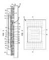
- FIG. 1is a diagrammatic sectional view depicting an assembly in accordance with one embodiment of the invention.
- FIG. 2is a top plan view of the assembly shown in FIG. 1 with some elements removed for clarity of illustration.
- FIGS. 3, 4 and 5are diagrammatic sectional views of assemblies according to further embodiments of the invention.
- an assemblyincludes a package element 10 having a top surface 12 and a bottom surface 14 .
- the package elementmay be a single-layer or multi-layer circuit panel incorporating one or more layers of a dielectric material and one or more layers of conductive features.
- the conductive featuresinclude stacked terminals 16 exposed at the bottom surface 14 , logic chip mounting pads 18 exposed at the top surface 12 , and MRAM chip mounting pads 20 .
- a terminal or other conductive featureis regarded as “exposed at” a surface of a dielectric element where the terminal is arranged so that all or part of the conductive feature can be seen by looking at such surface.
- a conductive feature which is exposed at a surface of a dielectric elementmay project from such surface; may be flush with such surface; or may be recessed from such surface and exposed through an opening extending entirely or partially through the dielectric element.
- the stack terminals 16are disposed in two stack terminal areas near opposite edges of the package element 10
- the MRAM chip mounting pads 20are disposed in an MRAM chip mounting area near the center of the bottom surface, between the stack terminal areas.
- the stack terminalscan be provided along all four edges of the package element as, for example, in an array forming a rectangular ring encircling the mounting pad area on the bottom surface of the package element.
- the logic chip mounting pads 18are omitted in FIG. 2 for clarity of illustration. At least some of the logic chip mounting pads 18 are connected to at least some of the MRAM chip mounting pads 20 as, for example, by vias 24 extending between the logic chip mounting pads and the MRAM chip mounting pads. Also, at least some of the logic chip mounting pads 18 are connected to at least some of the stack terminals 16 as, for example, by traces 26 extending on package element 10 .
- a statement that a feature is located “on” an elementdoes not necessarily mean that the feature is disposed on a surface of such element.
- traces 26may be disposed on the top surface or bottom surface of package element 10 , or may be disposed inside of such element.
- the MRAM chip mounting pads 20 and logic chip mounting pads 18which are connected to one another, are also aligned with one another so that they may be interconnected by very short vias extending vertically through the package element, with or without short additional traces extending in horizontal directions parallel to the surfaces of the package element.
- a common padmay be exposed at both top and bottom surfaces of the package element so that the same pad serves both as a logic chip mounting pad and as an MRAM chip mounting pad.
- Some of the MRAM chip mounting pads 20may be connected to some of the stack terminals 16 by additional conductive elements (not shown).
- Package element 10optionally may have additional features such as conductive ground planes (not shown).
- a first logic chip 26in this embodiment an FPGA chip, having a front face 28 with contacts 30 thereon and an oppositely-directed rear face 32 is mounted front-face down on top of package element 10 , so that the first logic chip overlies the top surface 12 of the package element.
- Some or, more typically, all of contacts 30 on the logic chipare aligned with some or, typically, all of the logic chip mounting pads 18 and bonded to such pads so that the contacts of the logic chip are electrically connected to the logic chip mounting pads.
- the contacts and padsmay be bonded by any conventional method as, for example, by diffusion bonding, soldering, eutectic bonding or the like.
- An encapsulant or underfill material 34desirably surrounds the front face and edges of the first logic chip 26 and also penetrates between the first logic chip and the package element in areas unoccupied by the connected pads and contacts.
- a thermally-conductive, desirably metallic heat spreader 36overlies the upwardly-facing rear surface 32 of the first logic chip and is in intimate thermal communication with the first logic chip.
- a thermally-conductive compositionsuch as an adhesive, gel or paste 38 , or a metallic bond such as a solder bond, connects the rear surface of the first logic chip to the thermal spreader.
- encapsulant underfill 34 and thermally-conductive filler 38are shown as physically separate elements, these elements may be formed from portions of the same material, or from portions of different materials which abut one another within the interior space 40 defined by the thermal spreader 36 .
- the subassembly of the first logic chip and package elementpreferably is prefabricated. That is, the package element 10 , along with the underfill and, optionally, the heat spreader 36 , act as a package for the first logic chip or FPGA 26 . Typically, such a subassembly is fabricated in a chip packaging plant associated with the FPGA manufacturer.
- the assemblyfurther includes a packaged MRAM chip 42 incorporating an MRAM chip 44 having a front face 46 , a rear face 48 and contacts 50 exposed at the front face.
- the packaged MRAM chip 42also includes an MRAM chip package substrate 52 bearing MRAM chip package terminals 54 separate from contacts 50 , but electrically connected thereto.
- MRAM chip package terminals 54overlie the front face 46 of the MRAM chip 44 itself and are connected to the contacts 50 of the MRAM chip by leads 58 .
- MRAM chip package terminals 54are exposed at the side of MRAM chip package substrate 52 facing away from the MRAM chip (facing upwardly in FIG. 1 ).
- the MRAM chip package terminalsmaybe disposed on the inwardly-facing side of the package substrate, but exposed through holes in the MRAM chip package substrate.
- the MRAM chip package substrate 52 and MRAM chip package terminals 54may be spaced form the front surface 46 of the MRAM chip by an intermediate layer 60 , which optionally may be a compliant layer.
- packaged MRAM chip 42is in the form of a low-profile, chip-size package having an area substantially equal to, or just slightly larger than, the areas of the MRAM chip surfaces themselves.
- the height or vertical dimension HMP of the MRAM chip package as a wholeis less than about 500 microns, preferably less than about 300 microns.
- the height HMP of the packaged MRAM chipdesirably exceeds the height or thickness of the MRAM chip 44 by about 200 microns or less, preferably about 150 microns or less.
- Suitable packaging arrangements for chips in general, which can be used to form the packaged MRAM chipare disclosed, for example, in U.S. Pat. Nos. 5,679,977; 5,489,749; and 5,915,752, the disclosures of which are hereby incorporated by reference herein.
- the packaged MRAM chipis pre-assembled in a packaging operation separate from the operations used to make the remaining components of the assembly, and the packaged MRAM chip can be sold, shipped and stacked.
- MRAM chips, per seare known in the art and are commercially available from sources such as Motorola and others.
- the packaged MRAM chipis mounted below the package element 10 so that the packaged MRAM chip occupies the MRAM chip mounting area and overlies the MRAM chip mounting pads 20 , and so that the MRAM chip package terminals 54 are aligned with the MRAM chip mounting pads.
- Thin layers of solderare other conductive bonding materials connect the MRAM chip package terminals 54 with the MRAM chip mounting pads 20 .
- Such a connectionis commonly referred to as a land grid array (“LGA”) and effectively minimizes the height H MP of the packaged MRAM chip.
- LGAland grid array
- the operation of attaching the packaged MRAM chip 42 to the packaged FPGAcan be performed using techniques similar to those used in surface-mounting chips to circuit boards, and may be performed either in the same plant which ultimately employs the assembly, as discussed, or in another plant.
- the packaged MRAM chip mounted to the package element 10the first MRAM chip 44 lies below the first logic chip or FPGA 26 , with the chips disposed in front-face-to-front-face orientation and with package element 10 disposed between the chips.
- the MRAM chip 44is interconnected with the first logic chip or FPGA 26 through the conductive features of the package element 10 , and through the MRAM chip package terminals 54 . These interconnections provide numerous signal paths between the MRAM chip and the first logic chip, such signal paths having short signal propagation times.
- the assembly discussed abovecan be mounted to a circuit panel such as a printed circuit board 62 having a top surface 64 and conductive features such as board mounting pad 66 exposed at the top surface.
- the assemblyoverlies the top surface with stack terminals 16 aligned with the board mounting pads and connected thereto by conductive attachments such as solder balls 68 .
- the entire assemblycan be mounted to the circuit panel in a single operation using generally conventional surface-mounting techniques.
- the conductive mounting elements or solder balls 68project downwardly from stack terminals 16 and support package element 10 above the top surface of the circuit panel so as to provide clearance for the packaged MRAM chip.
- circuit panel 66is a conventional circuit board. However, other types of circuit panels may be employed. For example, circuit panel 66 itself may be the substrate of a multi-chip module or other subassembly which, in turn, can be mounted to a larger circuit panel. Also, circuit panel 66 may be part of another element, such as, for example, a large semiconductor chip.
- the MRAM chip and FPGA or first logic chipact as a self-contained system which communicates with the larger assembly through stack terminals 16 and the associated elements of the circuit panel.
- the circuit panel 62need not provide for interconnections between the MRAM chip and the first logic chip.
- the combination including the MRAM chipprovides a unique advantage, in that the MRAM chip has substantially lower power dissipation than other forms of memory having comparable speed and memory density (or number of memory elements per unit volume).
- the MRAM chipdissipates substantially less power than SRAM or DRAM chips of comparable memory density and size. This difference in power dissipation is particularly important in a stacked arrangement as shown, where heat must be dissipated from both the memory chip and the logic chip.
- Packaged logic chips or FPGAs 26 of a given design and including a package element 10 of a given designmay be assembled with MRAM chips of varying capacities to provide assemblies having different capabilities, as desired to meet particular requirements.
- the different MRAM chipscan be provided with MRAM chip package substrates 52 having MRAM chip terminals 54 in the same arrangement, so that all are compatible with a given package element 10 .
- the assembliescan be made as needed in a surface-mounting plant, so that there is no need to stock prepackaged assemblies with different MRAM chips for different applications.
- a “bare” or unpackaged MRAM chipcan be substituted for the packaged MRAM chip depicted.
- the MRAM chipsneed not be in the front-face-to-front-face orientation shown.
- the logic chip or FPGAmay be mounted “face-up” on the package element 10 and connected to the connective features of the package element by leads such as wire bonds.
- the MRAM chipmay be mounted with its front face facing away from the MRAM chip package substrate (where employed) or facing away from package element 10 .
- the MRAM chiplies at the bottom of the stack, whereas the logic chip or FPGA lies at the top of the stack, above the MRAM chip. This arrangement can be reversed, so that the logic chip lies below the MRAM chip.
- a bare or unpackaged MRAM chip 144is mounted face-to-face with a bare or unpackaged logic chip or FPGA 126 , and some of the terminals of the FPGA are connected to terminals of the MRAM chips by bonds 102 .
- the rear surface of the FPGAoverlies a package element 110 bearing stack terminals 116 , which, in turn, are connected to contacts of the FPGA lying outside of the area covered by the MRAM chip using leads such as wire bonds 104 .
- the stack terminals 116may be arranged for surface-mounting to a circuit panel (not shown) using a low-height bonding method such as an LGA.
- the package elementmay include a thermal conductor 106 which is exposed at the bottom surface of the package element as, for example, through a hole in the dielectric layer of the package element.
- a thermal conductormay be bonded to a thermally-conductive element of the circuit panel, such as a large metallic pad, to provide greater heat dissipation from the stack, thus compounding the advantages obtained through the use of an MRAM chip in the stack.
- a simpler stacked assemblyincludes a top chip 244 , which, in this case, is an MRAM chip, mounted directly on a bottom chip 226 , in this case a logic chip.
- the contact-bearing front face 246 of the MRAM chip and the contact-bearing front face 228 of the logic chipboth face upwardly.
- the rear face 248 of the MRAM chipis bonded to the front face of the logic chip 226 .
- the chipsare interconnected to one another by wire bonds 202 extending between the contacts of the two chips.
- the terminals for the stackare provided by some of the contacts 230 of the logic chip itself.
- the exposed contacts 230 of the logic chipcan be connected to pads 266 of the circuit panel by further wire bonds 204 .
- the stack assemblydoes not include a separate package element.
- stacked semiconductor chipsNumerous other physical configurations incorporating stacked semiconductor chips are possible.
- a stacked arrangementcan be made by securing a plurality of chips to a substrate and folding the substrate so that the chips overlie one another.
- the disclosures of these patents and applicationsare hereby incorporated by reference herein.
- Certain other stacked chip arrangementsare disclosed in the aforementioned '977 patent and in U.S. Pat. No. 5,148,265, the disclosure of which is hereby incorporated by reference herein. All of these stacked arrangements may be employed.
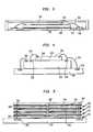
- a stacked chip assemblyin another configuration ( FIG. 5 ), includes a plurality of units which are similar to one another.
- Each unitincludes one or more chips 346 and a unit substrate 310 having unit terminals 304 thereon.
- the unit terminals 304 of each such unitare connected to the chip or chips included in that unit as, for example, by traces and leads 308 carried on the unit substrate.
- the unit terminalsare arranged so that connections can be made to these terminals either from above or below the unit.
- Plural unitsare superposed on one another and connected by inter-unit connecting elements such as solder balls 309 , so as to form a stacked assembly.
- the unit interconnect elementsform vertical buses which connect the chips in the various units to one another.
- busescan be connected by stack-mounting elements 368 to pads 366 on a circuit panel 362 .
- Arrangements of this typecan be used with various types of chips, but are particularly useful in arrangements where some or all of the chips in the various units are identical to one another as, for example, in stacks incorporating plural memory chips. Multi-unit stacks are further discussed in co-pending, commonly assigned U.S. patent application Ser. Nos. 10/267,450 and 10/454,029, the disclosures of which are also hereby incorporated by reference herein.
- all of the chips in the stackmay be MRAM chips.
- MRAM chipsare particularly advantageous in a multi-unit stack containing plural memory chips, because, here again, the low power dissipation of MRAM chips simplifies the task of cooling the chips in the stack.
- the low power dissipation of the MRAM chipscan allow for greater stack heights with more chips than could be accommodated in a comparable stack of SRAM or DRAM chips.
- MRAM chips in such a memory stackcan eliminate the need for special cooling measures such as mist cooling or forced air circulation required for a comparable DRAM or SRAM stack.
Landscapes
- Engineering & Computer Science (AREA)
- Power Engineering (AREA)
- Microelectronics & Electronic Packaging (AREA)
- Physics & Mathematics (AREA)
- Condensed Matter Physics & Semiconductors (AREA)
- General Physics & Mathematics (AREA)
- Computer Hardware Design (AREA)
- Semiconductor Memories (AREA)
- Mram Or Spin Memory Techniques (AREA)
Abstract
Description
- The present application claims the benefit of the filing date of U.S. Provisional Patent Application No. 60/532,213 filed Dec. 23, 2003, the disclosure of which is hereby incorporated herein by reference.
- Semiconductor chips are commonly provided in packages which physically protect the semiconductor chip itself and which facilitate mounting of the chip to a circuit panel. Significant development has occurred in such packages, so as to reduce the size of the package relative to the size of the chip itself, and to provide packages which are compatible with modern circuit panel assembly techniques such as surface-mounting.
- Semiconductor chips ordinarily are generally planar, thin elements having a front surface with contacts thereon connected to the internal semiconductor elements of the chips, an opposite, rear surface and edges extending between these front and rear surfaces. As used herein with reference to a semiconductor chip, the term “area” refers to the area of the front or rear surface of the chip. Certain chips, commonly referred to as “chip size packages” occupy an area of the circuit panel equal to the area of the chip itself, or only slightly larger than the area of the chip itself. Certain semiconductor chips have been provided heretofore in stacked arrangements so that the chips are superposed on one another, with the front or rear surface of one chip facing toward the front or rear surface of another chip. In many cases, the chips are functionally related to one another, so that they must be interconnected to one another. Such a stacked assembly can incorporate some or all of the required interconnections between the chips and, in some cases, can be prefabricated so that the stacked assembly may be handled, stocked and assembled to a larger circuit panel as a unit.
- Stacking chips in this manner reduces the aggregate area of the circuit panel occupied by the chips. However, stacked chip arrangements suffer from some drawbacks with respect to heat dissipation. All else being equal, two chips mounted in a stacked arrangement will normally have higher internal temperatures than two individual chips mounted on separate portions of the circuit board. In some cases, this drawback precludes the use of stacked chips or requires expensive special cooling measures.
- It is particularly desirable to provide a logic chip such as a processor or, particularly, a field programmable gate array (“FPGA”) in a stacked package with memory used in conjunction with the logic chip. FPGAs typically are used with external memory chips. In some cases, the FPGA incorporates a small internal memory adequate for some applications, but not adequate for all applications. In other cases, the FPGA incorporates no internal memory at all. Because the FPGA exchanges large amounts of data at frequent intervals with the external memory, it is important to minimize signal propagation delays between the FPGA and the external memory chip. Also, numerous signal lines are required for this data interchange. If the FPGA and the external memory chip are both mounted separately on a circuit panel, the circuit panel must accommodate all of these signal lines, which may require a complex circuit panel with numerous layers of conductive traces. This, in turn, significantly increases the costs and reduces the reliability of the overall assembly.
- One aspect of the present invention incorporates the realization that magnetic random access memory chips (hereinafter “MRAM chips”) are uniquely well-suited for mounting in stacked arrangements. As further discussed below, a semiconductor assembly according to this aspect of the invention desirably includes a bottom chip and one or more upper chips superposed on the bottom chip, so that the chips constitute a stack, at least one of the chips in the stack being a first MRAM chip. The assembly according to this aspect of the invention further includes stack terminals connected to at least one of the chips in the stack, the stack terminals being adapted to connect the chips to a circuit panel when the stack is mounted to a circuit panel with the bottom chip adjacent the circuit panel.
- In a particularly preferred arrangement, the chips in the stack include a first logic chip which is electrically connected to the first MRAM chip. These two chips may be the only chips in the only stack or, alternatively, additional chips can be provided. The assembly may include a package element in the form of a small circuit panel bearing the stack terminals and other conductive features discussed below. The FPGA may be directly and permanently mounted to the package element. Stated another way, the package element may serve as a part of the package for the FPGA chip. For example, the FPGA chip may be provided pre-assembled to the package element of the stacked assembly by the FPGA manufacturer. This allows a circuit designer to select different MRAM chips for inclusion in a stack used for different applications. Typically, the separate MRAM chip is provided in a separate MRAM package, which can be mounted to the pre-assembled FPGA chip and package element
FIG. 1 is a diagrammatic sectional view depicting an assembly in accordance with one embodiment of the invention.FIG. 2 is a top plan view of the assembly shown inFIG. 1 with some elements removed for clarity of illustration.FIGS. 3, 4 and5 are diagrammatic sectional views of assemblies according to further embodiments of the invention.- As seen in
FIG. 1 , an assembly according to one embodiment of the invention includes apackage element 10 having atop surface 12 and abottom surface 14. The package element may be a single-layer or multi-layer circuit panel incorporating one or more layers of a dielectric material and one or more layers of conductive features. The conductive features include stackedterminals 16 exposed at thebottom surface 14, logicchip mounting pads 18 exposed at thetop surface 12, and MRAMchip mounting pads 20. As used in this disclosure, a terminal or other conductive feature is regarded as “exposed at” a surface of a dielectric element where the terminal is arranged so that all or part of the conductive feature can be seen by looking at such surface. Thus, a conductive feature which is exposed at a surface of a dielectric element may project from such surface; may be flush with such surface; or may be recessed from such surface and exposed through an opening extending entirely or partially through the dielectric element. As best seen inFIG. 2 , thestack terminals 16 are disposed in two stack terminal areas near opposite edges of thepackage element 10, whereas the MRAMchip mounting pads 20 are disposed in an MRAM chip mounting area near the center of the bottom surface, between the stack terminal areas. - In a variant, the stack terminals can be provided along all four edges of the package element as, for example, in an array forming a rectangular ring encircling the mounting pad area on the bottom surface of the package element. The logic
chip mounting pads 18 are omitted inFIG. 2 for clarity of illustration. At least some of the logicchip mounting pads 18 are connected to at least some of the MRAMchip mounting pads 20 as, for example, byvias 24 extending between the logic chip mounting pads and the MRAM chip mounting pads. Also, at least some of the logicchip mounting pads 18 are connected to at least some of thestack terminals 16 as, for example, bytraces 26 extending onpackage element 10. As used in this disclosure, a statement that a feature is located “on” an element does not necessarily mean that the feature is disposed on a surface of such element. For example,traces 26 may be disposed on the top surface or bottom surface ofpackage element 10, or may be disposed inside of such element. - Desirably, at least some of the MRAM
chip mounting pads 20 and logicchip mounting pads 18, which are connected to one another, are also aligned with one another so that they may be interconnected by very short vias extending vertically through the package element, with or without short additional traces extending in horizontal directions parallel to the surfaces of the package element. Indeed, a common pad may be exposed at both top and bottom surfaces of the package element so that the same pad serves both as a logic chip mounting pad and as an MRAM chip mounting pad. Some of the MRAMchip mounting pads 20 may be connected to some of thestack terminals 16 by additional conductive elements (not shown).Package element 10 optionally may have additional features such as conductive ground planes (not shown). - A
first logic chip 26, in this embodiment an FPGA chip, having afront face 28 withcontacts 30 thereon and an oppositely-directedrear face 32 is mounted front-face down on top ofpackage element 10, so that the first logic chip overlies thetop surface 12 of the package element. Some or, more typically, all ofcontacts 30 on the logic chip are aligned with some or, typically, all of the logicchip mounting pads 18 and bonded to such pads so that the contacts of the logic chip are electrically connected to the logic chip mounting pads. The contacts and pads may be bonded by any conventional method as, for example, by diffusion bonding, soldering, eutectic bonding or the like. An encapsulant orunderfill material 34 desirably surrounds the front face and edges of thefirst logic chip 26 and also penetrates between the first logic chip and the package element in areas unoccupied by the connected pads and contacts. - A thermally-conductive, desirably
metallic heat spreader 36 overlies the upwardly-facingrear surface 32 of the first logic chip and is in intimate thermal communication with the first logic chip. Preferably, a thermally-conductive composition such as an adhesive, gel orpaste 38, or a metallic bond such as a solder bond, connects the rear surface of the first logic chip to the thermal spreader. Althoughencapsulant underfill 34 and thermally-conductive filler 38 are shown as physically separate elements, these elements may be formed from portions of the same material, or from portions of different materials which abut one another within theinterior space 40 defined by thethermal spreader 36. - The subassembly of the first logic chip and package element preferably is prefabricated. That is, the
package element 10, along with the underfill and, optionally, theheat spreader 36, act as a package for the first logic chip orFPGA 26. Typically, such a subassembly is fabricated in a chip packaging plant associated with the FPGA manufacturer. - The assembly further includes a packaged
MRAM chip 42 incorporating anMRAM chip 44 having afront face 46, arear face 48 andcontacts 50 exposed at the front face. The packagedMRAM chip 42 also includes an MRAMchip package substrate 52 bearing MRAMchip package terminals 54 separate fromcontacts 50, but electrically connected thereto. MRAMchip package terminals 54 overlie thefront face 46 of theMRAM chip 44 itself and are connected to thecontacts 50 of the MRAM chip by leads58. MRAMchip package terminals 54 are exposed at the side of MRAMchip package substrate 52 facing away from the MRAM chip (facing upwardly inFIG. 1 ). For example, the MRAM chip package terminals maybe disposed on the inwardly-facing side of the package substrate, but exposed through holes in the MRAM chip package substrate. The MRAMchip package substrate 52 and MRAMchip package terminals 54 may be spaced form thefront surface 46 of the MRAM chip by anintermediate layer 60, which optionally may be a compliant layer. Most preferably, packagedMRAM chip 42 is in the form of a low-profile, chip-size package having an area substantially equal to, or just slightly larger than, the areas of the MRAM chip surfaces themselves. - Desirably, the height or vertical dimension HMP of the MRAM chip package as a whole is less than about 500 microns, preferably less than about 300 microns. The height HMP of the packaged MRAM chip desirably exceeds the height or thickness of the
MRAM chip 44 by about 200 microns or less, preferably about 150 microns or less. - Suitable packaging arrangements for chips in general, which can be used to form the packaged MRAM chip, are disclosed, for example, in U.S. Pat. Nos. 5,679,977; 5,489,749; and 5,915,752, the disclosures of which are hereby incorporated by reference herein. Typically, the packaged MRAM chip is pre-assembled in a packaging operation separate from the operations used to make the remaining components of the assembly, and the packaged MRAM chip can be sold, shipped and stacked. MRAM chips, per se, are known in the art and are commercially available from sources such as Motorola and others.
- The packaged MRAM chip is mounted below the
package element 10 so that the packaged MRAM chip occupies the MRAM chip mounting area and overlies the MRAMchip mounting pads 20, and so that the MRAMchip package terminals 54 are aligned with the MRAM chip mounting pads. Thin layers of solder are other conductive bonding materials connect the MRAMchip package terminals 54 with the MRAMchip mounting pads 20. Such a connection is commonly referred to as a land grid array (“LGA”) and effectively minimizes the height HMPof the packaged MRAM chip. - The operation of attaching the packaged
MRAM chip 42 to the packaged FPGA (chip 26 and package element10) can be performed using techniques similar to those used in surface-mounting chips to circuit boards, and may be performed either in the same plant which ultimately employs the assembly, as discussed, or in another plant. With the packaged MRAM chip mounted to thepackage element 10, thefirst MRAM chip 44 lies below the first logic chip orFPGA 26, with the chips disposed in front-face-to-front-face orientation and withpackage element 10 disposed between the chips. TheMRAM chip 44 is interconnected with the first logic chip orFPGA 26 through the conductive features of thepackage element 10, and through the MRAMchip package terminals 54. These interconnections provide numerous signal paths between the MRAM chip and the first logic chip, such signal paths having short signal propagation times. - The assembly discussed above can be mounted to a circuit panel such as a printed
circuit board 62 having atop surface 64 and conductive features such asboard mounting pad 66 exposed at the top surface. The assembly overlies the top surface withstack terminals 16 aligned with the board mounting pads and connected thereto by conductive attachments such assolder balls 68. The entire assembly can be mounted to the circuit panel in a single operation using generally conventional surface-mounting techniques. In the completed assembly, the conductive mounting elements orsolder balls 68 project downwardly fromstack terminals 16 andsupport package element 10 above the top surface of the circuit panel so as to provide clearance for the packaged MRAM chip. Theboard mounting pads 66 are connected to other elements of a larger electronic device (not shown) by traces or other conductive features (not shown) on thecircuit panel 66. As depicted,circuit panel 66 is a conventional circuit board. However, other types of circuit panels may be employed. For example,circuit panel 66 itself may be the substrate of a multi-chip module or other subassembly which, in turn, can be mounted to a larger circuit panel. Also,circuit panel 66 may be part of another element, such as, for example, a large semiconductor chip. - In operation, the MRAM chip and FPGA or first logic chip act as a self-contained system which communicates with the larger assembly through
stack terminals 16 and the associated elements of the circuit panel. Thecircuit panel 62 need not provide for interconnections between the MRAM chip and the first logic chip. Moreover, the combination including the MRAM chip provides a unique advantage, in that the MRAM chip has substantially lower power dissipation than other forms of memory having comparable speed and memory density (or number of memory elements per unit volume). For example, the MRAM chip dissipates substantially less power than SRAM or DRAM chips of comparable memory density and size. This difference in power dissipation is particularly important in a stacked arrangement as shown, where heat must be dissipated from both the memory chip and the logic chip. - Use of a separately-packaged MRAM chip as an element in the assembly provides considerable versatility. Packaged logic chips or
FPGAs 26 of a given design and including apackage element 10 of a given design may be assembled with MRAM chips of varying capacities to provide assemblies having different capabilities, as desired to meet particular requirements. The different MRAM chips can be provided with MRAMchip package substrates 52 havingMRAM chip terminals 54 in the same arrangement, so that all are compatible with a givenpackage element 10. The assemblies can be made as needed in a surface-mounting plant, so that there is no need to stock prepackaged assemblies with different MRAM chips for different applications. - Numerous variations and combinations of the features discussed above can be employed. For example, a “bare” or unpackaged MRAM chip can be substituted for the packaged MRAM chip depicted. Further, the MRAM chips need not be in the front-face-to-front-face orientation shown. For example, the logic chip or FPGA may be mounted “face-up” on the
package element 10 and connected to the connective features of the package element by leads such as wire bonds. Similarly, the MRAM chip may be mounted with its front face facing away from the MRAM chip package substrate (where employed) or facing away frompackage element 10. In the embodiment depicted inFIGS. 1 and 2 , the MRAM chip lies at the bottom of the stack, whereas the logic chip or FPGA lies at the top of the stack, above the MRAM chip. This arrangement can be reversed, so that the logic chip lies below the MRAM chip. - Other stack packaging arrangements may be employed. For example, in the assembly of
FIG. 3 , a bare orunpackaged MRAM chip 144 is mounted face-to-face with a bare or unpackaged logic chip orFPGA 126, and some of the terminals of the FPGA are connected to terminals of the MRAM chips bybonds 102. The rear surface of the FPGA overlies apackage element 110bearing stack terminals 116, which, in turn, are connected to contacts of the FPGA lying outside of the area covered by the MRAM chip using leads such as wire bonds104. In this arrangement, thestack terminals 116 may be arranged for surface-mounting to a circuit panel (not shown) using a low-height bonding method such as an LGA. Also, as described more fully in co-pending U.S. patent application Ser. Nos. 10/210,160 and 60/462,170, the disclosures of which are hereby incorporated by reference herein, the package element may include athermal conductor 106 which is exposed at the bottom surface of the package element as, for example, through a hole in the dielectric layer of the package element. Such a thermal conductor may be bonded to a thermally-conductive element of the circuit panel, such as a large metallic pad, to provide greater heat dissipation from the stack, thus compounding the advantages obtained through the use of an MRAM chip in the stack. - As seen in
FIG. 4 , a simpler stacked assembly includes atop chip 244, which, in this case, is an MRAM chip, mounted directly on abottom chip 226, in this case a logic chip. The contact-bearingfront face 246 of the MRAM chip and the contact-bearingfront face 228 of the logic chip both face upwardly. Therear face 248 of the MRAM chip is bonded to the front face of thelogic chip 226. The chips are interconnected to one another bywire bonds 202 extending between the contacts of the two chips. In this case, the terminals for the stack are provided by some of thecontacts 230 of the logic chip itself. When the stack is mounted on acircuit panel 262, the exposedcontacts 230 of the logic chip can be connected topads 266 of the circuit panel byfurther wire bonds 204. Thus, in this case, the stack assembly does not include a separate package element. - Numerous other physical configurations incorporating stacked semiconductor chips are possible. For example, as disclosed in U.S. Pat. No. 6,225,688 and in co-pending, commonly assigned U.S. patent application Ser. Nos. 10/281,550; 10/077,388; 10/655,952; 10/640,177; and 10/654,375, a stacked arrangement can be made by securing a plurality of chips to a substrate and folding the substrate so that the chips overlie one another. The disclosures of these patents and applications are hereby incorporated by reference herein. Certain other stacked chip arrangements are disclosed in the aforementioned '977 patent and in U.S. Pat. No. 5,148,265, the disclosure of which is hereby incorporated by reference herein. All of these stacked arrangements may be employed.
- In another configuration (
FIG. 5 ), a stacked chip assembly includes a plurality of units which are similar to one another. Each unit includes one ormore chips 346 and aunit substrate 310 havingunit terminals 304 thereon. Theunit terminals 304 of each such unit are connected to the chip or chips included in that unit as, for example, by traces and leads308 carried on the unit substrate. The unit terminals are arranged so that connections can be made to these terminals either from above or below the unit. Plural units are superposed on one another and connected by inter-unit connecting elements such assolder balls 309, so as to form a stacked assembly. The unit interconnect elements form vertical buses which connect the chips in the various units to one another. These buses can be connected by stack-mountingelements 368 topads 366 on acircuit panel 362. Arrangements of this type can be used with various types of chips, but are particularly useful in arrangements where some or all of the chips in the various units are identical to one another as, for example, in stacks incorporating plural memory chips. Multi-unit stacks are further discussed in co-pending, commonly assigned U.S. patent application Ser. Nos. 10/267,450 and 10/454,029, the disclosures of which are also hereby incorporated by reference herein. - In the embodiment of
FIG. 5 , all of the chips in the stack may be MRAM chips. Such a stack can be used to provide a compact, high-capacity MRAM chip unit which can be mounted on a small area of the circuit panel. MRAM chips are particularly advantageous in a multi-unit stack containing plural memory chips, because, here again, the low power dissipation of MRAM chips simplifies the task of cooling the chips in the stack. In this embodiment as well, the low power dissipation of the MRAM chips can allow for greater stack heights with more chips than could be accommodated in a comparable stack of SRAM or DRAM chips. Conversely, the use of MRAM chips in such a memory stack can eliminate the need for special cooling measures such as mist cooling or forced air circulation required for a comparable DRAM or SRAM stack. These advantages are particularly pronounced in a system which incorporates plural stacks of chips on a circuit board or on a module substrate, as taught, for example, in co-pending, commonly assigned U.S. Provisional Patent Application Ser. Nos. 60/490,802 and 60/517,179, the disclosures of which are also incorporated by reference herein. - As these and other variations and combinations of the features discussed above can be utilized without departing from the present invention, the foregoing description of the preferred embodiments should be taken by way of illustration rather than by way of limitation of the invention as defined by the claims.
Claims (19)
Priority Applications (1)
| Application Number | Priority Date | Filing Date | Title |
|---|---|---|---|
| US11/018,969US7521785B2 (en) | 2003-12-23 | 2004-12-21 | Packaged systems with MRAM |
Applications Claiming Priority (2)
| Application Number | Priority Date | Filing Date | Title |
|---|---|---|---|
| US53221303P | 2003-12-23 | 2003-12-23 | |
| US11/018,969US7521785B2 (en) | 2003-12-23 | 2004-12-21 | Packaged systems with MRAM |
Publications (2)
| Publication Number | Publication Date |
|---|---|
| US20050184399A1true US20050184399A1 (en) | 2005-08-25 |
| US7521785B2 US7521785B2 (en) | 2009-04-21 |
Family
ID=34863733
Family Applications (1)
| Application Number | Title | Priority Date | Filing Date |
|---|---|---|---|
| US11/018,969Expired - LifetimeUS7521785B2 (en) | 2003-12-23 | 2004-12-21 | Packaged systems with MRAM |
Country Status (1)
| Country | Link |
|---|---|
| US (1) | US7521785B2 (en) |
Cited By (9)
| Publication number | Priority date | Publication date | Assignee | Title |
|---|---|---|---|---|
| US20100077244A1 (en)* | 2008-09-23 | 2010-03-25 | Qualcomm Incorporated | Low power electronic system architecture using non-volatile magnetic memory |
| US20110304036A1 (en)* | 2010-06-09 | 2011-12-15 | Hynix Semiconductor Inc. | Semiconductor package with heat dissipation devices |
| US20120068229A1 (en)* | 2009-05-06 | 2012-03-22 | Majid Bemanian | Massively Parallel Interconnect Fabric for Complex Semiconductor Devices |
| US8294252B1 (en)* | 2006-08-31 | 2012-10-23 | Altera Corporation | Stacked semiconductor substrates |
| US8716876B1 (en)* | 2011-11-11 | 2014-05-06 | Altera Corporation | Systems and methods for stacking a memory chip above an integrated circuit chip |
| US20150221601A1 (en)* | 2014-02-05 | 2015-08-06 | Amkor Technology, Inc. | Semiconductor device with redistribution layers formed utilizing dummy substrates |
| US20160148913A1 (en)* | 2007-05-08 | 2016-05-26 | Tae-Joo Hwang | Semiconductor package and method of forming the same |
| KR101679359B1 (en) | 2010-05-27 | 2016-11-25 | 삼성전자 주식회사 | Controlling Method for non-volatile memory device |
| US20170109551A1 (en)* | 2014-03-18 | 2017-04-20 | Hewlett-Packard Development Company, L.P. | Secure element |
Families Citing this family (4)
| Publication number | Priority date | Publication date | Assignee | Title |
|---|---|---|---|---|
| US6551857B2 (en) | 1997-04-04 | 2003-04-22 | Elm Technology Corporation | Three dimensional structure integrated circuits |
| AU2003255254A1 (en) | 2002-08-08 | 2004-02-25 | Glenn J. Leedy | Vertical system integration |
| TW200905835A (en)* | 2007-07-26 | 2009-02-01 | En-Min Jow | Connector with build-in control unit and its application |
| TWI470762B (en) | 2007-07-27 | 2015-01-21 | 尼康股份有限公司 | Laminated semiconductor device |
Citations (13)
| Publication number | Priority date | Publication date | Assignee | Title |
|---|---|---|---|---|
| US5138438A (en)* | 1987-06-24 | 1992-08-11 | Akita Electronics Co. Ltd. | Lead connections means for stacked tab packaged IC chips |
| US5148265A (en)* | 1990-09-24 | 1992-09-15 | Ist Associates, Inc. | Semiconductor chip assemblies with fan-in leads |
| US5148266A (en)* | 1990-09-24 | 1992-09-15 | Ist Associates, Inc. | Semiconductor chip assemblies having interposer and flexible lead |
| US5165265A (en)* | 1992-02-20 | 1992-11-24 | Alvin Maionchi | Trailer security lock apparatus |
| US5489749A (en)* | 1992-07-24 | 1996-02-06 | Tessera, Inc. | Semiconductor connection components and method with releasable lead support |
| US5608262A (en)* | 1995-02-24 | 1997-03-04 | Lucent Technologies Inc. | Packaging multi-chip modules without wire-bond interconnection |
| US5679977A (en)* | 1990-09-24 | 1997-10-21 | Tessera, Inc. | Semiconductor chip assemblies, methods of making same and components for same |
| US5801072A (en)* | 1996-03-14 | 1998-09-01 | Lsi Logic Corporation | Method of packaging integrated circuits |
| US5869894A (en)* | 1997-07-18 | 1999-02-09 | Lucent Technologies Inc. | RF IC package |
| US6225688B1 (en)* | 1997-12-11 | 2001-05-01 | Tessera, Inc. | Stacked microelectronic assembly and method therefor |
| US6417688B1 (en)* | 1999-12-31 | 2002-07-09 | Intel Corporation | Method and apparatus for implementing a highly robust, fast, and economical five load bus topology based on bit mirroring and a well terminated transmission environment |
| US6462421B1 (en)* | 2000-04-10 | 2002-10-08 | Advanced Semicondcutor Engineering, Inc. | Multichip module |
| US6555917B1 (en)* | 2001-10-09 | 2003-04-29 | Amkor Technology, Inc. | Semiconductor package having stacked semiconductor chips and method of making the same |
Family Cites Families (1)
| Publication number | Priority date | Publication date | Assignee | Title |
|---|---|---|---|---|
| WO2004034434A2 (en) | 2002-10-11 | 2004-04-22 | Tessera, Inc. | Components, methods and assemblies for multi-chip packages |
- 2004
- 2004-12-21USUS11/018,969patent/US7521785B2/ennot_activeExpired - Lifetime
Patent Citations (14)
| Publication number | Priority date | Publication date | Assignee | Title |
|---|---|---|---|---|
| US5138438A (en)* | 1987-06-24 | 1992-08-11 | Akita Electronics Co. Ltd. | Lead connections means for stacked tab packaged IC chips |
| US5679977A (en)* | 1990-09-24 | 1997-10-21 | Tessera, Inc. | Semiconductor chip assemblies, methods of making same and components for same |
| US5148265A (en)* | 1990-09-24 | 1992-09-15 | Ist Associates, Inc. | Semiconductor chip assemblies with fan-in leads |
| US5148266A (en)* | 1990-09-24 | 1992-09-15 | Ist Associates, Inc. | Semiconductor chip assemblies having interposer and flexible lead |
| US5165265A (en)* | 1992-02-20 | 1992-11-24 | Alvin Maionchi | Trailer security lock apparatus |
| US5489749A (en)* | 1992-07-24 | 1996-02-06 | Tessera, Inc. | Semiconductor connection components and method with releasable lead support |
| US5915752A (en)* | 1992-07-24 | 1999-06-29 | Tessera, Inc. | Method of making connections to a semiconductor chip assembly |
| US5608262A (en)* | 1995-02-24 | 1997-03-04 | Lucent Technologies Inc. | Packaging multi-chip modules without wire-bond interconnection |
| US5801072A (en)* | 1996-03-14 | 1998-09-01 | Lsi Logic Corporation | Method of packaging integrated circuits |
| US5869894A (en)* | 1997-07-18 | 1999-02-09 | Lucent Technologies Inc. | RF IC package |
| US6225688B1 (en)* | 1997-12-11 | 2001-05-01 | Tessera, Inc. | Stacked microelectronic assembly and method therefor |
| US6417688B1 (en)* | 1999-12-31 | 2002-07-09 | Intel Corporation | Method and apparatus for implementing a highly robust, fast, and economical five load bus topology based on bit mirroring and a well terminated transmission environment |
| US6462421B1 (en)* | 2000-04-10 | 2002-10-08 | Advanced Semicondcutor Engineering, Inc. | Multichip module |
| US6555917B1 (en)* | 2001-10-09 | 2003-04-29 | Amkor Technology, Inc. | Semiconductor package having stacked semiconductor chips and method of making the same |
Cited By (21)
| Publication number | Priority date | Publication date | Assignee | Title |
|---|---|---|---|---|
| US8294252B1 (en)* | 2006-08-31 | 2012-10-23 | Altera Corporation | Stacked semiconductor substrates |
| US20160148913A1 (en)* | 2007-05-08 | 2016-05-26 | Tae-Joo Hwang | Semiconductor package and method of forming the same |
| US9685400B2 (en)* | 2007-05-08 | 2017-06-20 | Samsung Electronics Co., Ltd. | Semiconductor package and method of forming the same |
| WO2010039458A1 (en)* | 2008-09-23 | 2010-04-08 | Qualcomm Incorporated | Low power electronic system using non-volatile magnetic memory |
| US20100077244A1 (en)* | 2008-09-23 | 2010-03-25 | Qualcomm Incorporated | Low power electronic system architecture using non-volatile magnetic memory |
| KR101262105B1 (en)* | 2008-09-23 | 2013-05-14 | 퀄컴 인코포레이티드 | Low power electronic system using non-volatile magnetic memory |
| TWI413895B (en)* | 2008-09-23 | 2013-11-01 | Qualcomm Inc | Method and low power electronic computing system using non volatile magnetic memory |
| US8719610B2 (en) | 2008-09-23 | 2014-05-06 | Qualcomm Incorporated | Low power electronic system architecture using non-volatile magnetic memory |
| RU2616171C2 (en)* | 2008-09-23 | 2017-04-12 | Квэлкомм Инкорпорейтед | Low power electronic system architecture using non-volatile magnetic memory |
| US20120068229A1 (en)* | 2009-05-06 | 2012-03-22 | Majid Bemanian | Massively Parallel Interconnect Fabric for Complex Semiconductor Devices |
| US9035443B2 (en)* | 2009-05-06 | 2015-05-19 | Majid Bemanian | Massively parallel interconnect fabric for complex semiconductor devices |
| KR101679359B1 (en) | 2010-05-27 | 2016-11-25 | 삼성전자 주식회사 | Controlling Method for non-volatile memory device |
| US8310045B2 (en)* | 2010-06-09 | 2012-11-13 | SK Hynix Inc. | Semiconductor package with heat dissipation devices |
| US20110304036A1 (en)* | 2010-06-09 | 2011-12-15 | Hynix Semiconductor Inc. | Semiconductor package with heat dissipation devices |
| US8716876B1 (en)* | 2011-11-11 | 2014-05-06 | Altera Corporation | Systems and methods for stacking a memory chip above an integrated circuit chip |
| US20150221601A1 (en)* | 2014-02-05 | 2015-08-06 | Amkor Technology, Inc. | Semiconductor device with redistribution layers formed utilizing dummy substrates |
| US10707181B2 (en)* | 2014-02-05 | 2020-07-07 | Amkor Technology Inc. | Semiconductor device with redistribution layers formed utilizing dummy substrates |
| US11600582B2 (en) | 2014-02-05 | 2023-03-07 | Amkor Technology Singapore Holding Pte. Ltd. | Semiconductor device with redistribution layers formed utilizing dummy substrates |
| US12388032B2 (en) | 2014-02-05 | 2025-08-12 | Amkor Technology Singapore Holding Pte. Ltd. | Semiconductor device with redistribution layers formed utilizing dummy substrates |
| US20170109551A1 (en)* | 2014-03-18 | 2017-04-20 | Hewlett-Packard Development Company, L.P. | Secure element |
| US9904814B2 (en)* | 2014-03-18 | 2018-02-27 | Hewlett-Packard Development Company, L.P. | Secure element |
Also Published As
| Publication number | Publication date |
|---|---|
| US7521785B2 (en) | 2009-04-21 |
Similar Documents
| Publication | Publication Date | Title |
|---|---|---|
| US7402911B2 (en) | Multi-chip device and method for producing a multi-chip device | |
| US6487078B2 (en) | Electronic module having a three dimensional array of carrier-mounted integrated circuit packages | |
| US6605875B2 (en) | Integrated circuit die having bond pads near adjacent sides to allow stacking of dice without regard to dice size | |
| US6300163B1 (en) | Stacked leads-over-chip multi-chip module | |
| US5811879A (en) | Stacked leads-over-chip multi-chip module | |
| KR100621991B1 (en) | Chip Scale Stacking Package | |
| US7309913B2 (en) | Stacked semiconductor packages | |
| US7061087B2 (en) | Multi-package stack module | |
| US6838768B2 (en) | Module assembly for stacked BGA packages | |
| US6388318B1 (en) | Surface mount-type package of ball grid array with multi-chip mounting | |
| US7276786B2 (en) | Stacked board-on-chip package having mirroring structure and dual inline memory module on which the stacked board-on-chip packages are mounted | |
| US20030137808A1 (en) | Electronic module having canopy-type carriers | |
| CN103620778A (en) | Flip-chip, face-up and face-down centerbond memory wirebond assemblies | |
| US7521785B2 (en) | Packaged systems with MRAM | |
| US6294838B1 (en) | Multi-chip stacked package | |
| US6023097A (en) | Stacked multiple-chip module micro ball grid array packaging | |
| US5872397A (en) | Semiconductor device package including a thick integrated circuit chip stack | |
| US6034425A (en) | Flat multiple-chip module micro ball grid array packaging | |
| US6803666B2 (en) | Semiconductor chip mounting substrate and semiconductor device using the same | |
| US8835218B2 (en) | Stackable layer containing ball grid array package | |
| US20070096333A1 (en) | Optimal stacked die organization |
Legal Events
| Date | Code | Title | Description |
|---|---|---|---|
| AS | Assignment | Owner name:TESSERA, INC., CALIFORNIA Free format text:ASSIGNMENT OF ASSIGNORS INTEREST;ASSIGNORS:DAMBERG, PHILIP;COLELLA, NICHOLAS J.;REEL/FRAME:016057/0573;SIGNING DATES FROM 20050224 TO 20050323 | |
| STCF | Information on status: patent grant | Free format text:PATENTED CASE | |
| FPAY | Fee payment | Year of fee payment:4 | |
| FPAY | Fee payment | Year of fee payment:8 | |
| AS | Assignment | Owner name:ROYAL BANK OF CANADA, AS COLLATERAL AGENT, CANADA Free format text:SECURITY INTEREST;ASSIGNORS:INVENSAS CORPORATION;TESSERA, INC.;TESSERA ADVANCED TECHNOLOGIES, INC.;AND OTHERS;REEL/FRAME:040797/0001 Effective date:20161201 | |
| AS | Assignment | Owner name:BANK OF AMERICA, N.A., NORTH CAROLINA Free format text:SECURITY INTEREST;ASSIGNORS:ROVI SOLUTIONS CORPORATION;ROVI TECHNOLOGIES CORPORATION;ROVI GUIDES, INC.;AND OTHERS;REEL/FRAME:053468/0001 Effective date:20200601 | |
| AS | Assignment | Owner name:INVENSAS BONDING TECHNOLOGIES, INC. (F/K/A ZIPTRONIX, INC.), CALIFORNIA Free format text:RELEASE BY SECURED PARTY;ASSIGNOR:ROYAL BANK OF CANADA;REEL/FRAME:052920/0001 Effective date:20200601 Owner name:DTS LLC, CALIFORNIA Free format text:RELEASE BY SECURED PARTY;ASSIGNOR:ROYAL BANK OF CANADA;REEL/FRAME:052920/0001 Effective date:20200601 Owner name:TESSERA, INC., CALIFORNIA Free format text:RELEASE BY SECURED PARTY;ASSIGNOR:ROYAL BANK OF CANADA;REEL/FRAME:052920/0001 Effective date:20200601 Owner name:FOTONATION CORPORATION (F/K/A DIGITALOPTICS CORPORATION AND F/K/A DIGITALOPTICS CORPORATION MEMS), CALIFORNIA Free format text:RELEASE BY SECURED PARTY;ASSIGNOR:ROYAL BANK OF CANADA;REEL/FRAME:052920/0001 Effective date:20200601 Owner name:PHORUS, INC., CALIFORNIA Free format text:RELEASE BY SECURED PARTY;ASSIGNOR:ROYAL BANK OF CANADA;REEL/FRAME:052920/0001 Effective date:20200601 Owner name:INVENSAS CORPORATION, CALIFORNIA Free format text:RELEASE BY SECURED PARTY;ASSIGNOR:ROYAL BANK OF CANADA;REEL/FRAME:052920/0001 Effective date:20200601 Owner name:DTS, INC., CALIFORNIA Free format text:RELEASE BY SECURED PARTY;ASSIGNOR:ROYAL BANK OF CANADA;REEL/FRAME:052920/0001 Effective date:20200601 Owner name:IBIQUITY DIGITAL CORPORATION, MARYLAND Free format text:RELEASE BY SECURED PARTY;ASSIGNOR:ROYAL BANK OF CANADA;REEL/FRAME:052920/0001 Effective date:20200601 Owner name:TESSERA ADVANCED TECHNOLOGIES, INC, CALIFORNIA Free format text:RELEASE BY SECURED PARTY;ASSIGNOR:ROYAL BANK OF CANADA;REEL/FRAME:052920/0001 Effective date:20200601 | |
| MAFP | Maintenance fee payment | Free format text:PAYMENT OF MAINTENANCE FEE, 12TH YEAR, LARGE ENTITY (ORIGINAL EVENT CODE: M1553); ENTITY STATUS OF PATENT OWNER: LARGE ENTITY Year of fee payment:12 |