US20050184337A1 - 4f2 eeprom nrom memory arrays with vertical devices - Google Patents
4f2 eeprom nrom memory arrays with vertical devicesDownload PDFInfo
- Publication number
- US20050184337A1 US20050184337A1US10/785,310US78531004AUS2005184337A1US 20050184337 A1US20050184337 A1US 20050184337A1US 78531004 AUS78531004 AUS 78531004AUS 2005184337 A1US2005184337 A1US 2005184337A1
- Authority
- US
- United States
- Prior art keywords
- forming
- nrom
- memory cell
- oxide
- nrom memory
- Prior art date
- Legal status (The legal status is an assumption and is not a legal conclusion. Google has not performed a legal analysis and makes no representation as to the accuracy of the status listed.)
- Granted
Links
Images


Classifications
- H—ELECTRICITY
- H10—SEMICONDUCTOR DEVICES; ELECTRIC SOLID-STATE DEVICES NOT OTHERWISE PROVIDED FOR
- H10B—ELECTRONIC MEMORY DEVICES
- H10B69/00—Erasable-and-programmable ROM [EPROM] devices not provided for in groups H10B41/00 - H10B63/00, e.g. ultraviolet erasable-and-programmable ROM [UVEPROM] devices
- H—ELECTRICITY
- H10—SEMICONDUCTOR DEVICES; ELECTRIC SOLID-STATE DEVICES NOT OTHERWISE PROVIDED FOR
- H10B—ELECTRONIC MEMORY DEVICES
- H10B43/00—EEPROM devices comprising charge-trapping gate insulators
- H10B43/30—EEPROM devices comprising charge-trapping gate insulators characterised by the memory core region
- B—PERFORMING OPERATIONS; TRANSPORTING
- B82—NANOTECHNOLOGY
- B82Y—SPECIFIC USES OR APPLICATIONS OF NANOSTRUCTURES; MEASUREMENT OR ANALYSIS OF NANOSTRUCTURES; MANUFACTURE OR TREATMENT OF NANOSTRUCTURES
- B82Y10/00—Nanotechnology for information processing, storage or transmission, e.g. quantum computing or single electron logic
Definitions
- the present inventionrelates generally to integrated circuits and in particular the present invention relates to EEPROM memory devices.
- RAMrandom-access memory
- RAMrandom-access memory
- ROMread-only memory
- Most RAMis volatile, which means that it requires a steady flow of electricity to maintain its contents. As soon as the power is turned off, whatever data was in RAM is lost.
- EEPROMelectrically erasable programmable read-only memory
- EEPROMelectrically erasable programmable read-only memory
- EEPROMcomprise a large number of memory cells having electrically isolated gates (floating gates). Data is stored in the memory cells in the form of charge on the floating gates. Charge is transported to or removed from the floating gates by specialized programming and erase operations, respectively.
- Flash memoryis a type of EEPROM that is typically erased and reprogrammed in blocks instead of one byte at a time.
- a typical Flash memorycomprises a memory array, which includes a large number of memory cells. Each of the memory cells includes a floating gate field-effect transistor capable of holding a charge. The data in a cell is determined by the presence or absence of the charge in the floating gate.
- the cellsare usually grouped into sections called “erase blocks.”
- the memory cells of a Flash memory arrayare typically arranged into a “NOR” architecture (each cell directly coupled to a bit line) or a “NAND” architecture (cells coupled into “strings” of cells, such that each cell is coupled indirectly to a bit line and requires activating the other cells of the string for access).
- Each of the cells within an erase blockcan be electrically programmed in a random basis by charging the floating gate. The charge can be removed from the floating gate by a block erase operation, wherein all floating gate memory cells in the erase block are erased in a single operation.
- NROMnitride read only memory
- FIG. 1illustrates a cross-sectional view of a typical prior art NROM memory cell with a channel length, L.
- the cellis comprised of a control gate 100 formed on top of an oxide-nitride-oxide (ONO) layer.
- This layeris comprised of an oxide layer 101 on top of a nitride 103 layer upon which the charge is stored for the various states of the cell.
- the cellhas trapping areas 105 and 106 for storing two bits of data on the nitride layer 103 .
- the nitride layer 103is deposited on another oxide layer 104 that is on the substrate.
- Two source/drain regions 109 and 111are at either end of the gate 100 .
- the source/drain regions 109 and 111are connected by a channel area 110 between the two source/drain regions 109 and 111 .
- the function of each source/drain region 109 or 111depends upon which bit trapping area 105 or 106 is being read or written. For example, in a read operation, if the carrier is input at the left side source/drain region 111 and output from the right side region 109 , the left side is the source 111 and the right side is the drain 109 and the data bit charge is stored on the nitride 103 at the source end 111 for bit trapping area 106 .
- the channel length of the NROM memory cells that make up the memory array and spacing between memory cells in the stringshave a large effect on the number of memory cells that can be placed in a given area and thus a direct impact on the density of the array and size of the resulting memory device.
- the feature sizes of the devicesare limited by the device characteristics before the minimum feature size that the process is capable of is reached.
- a minimum sizeis typically reached that is primarily dictated by the device operational characteristics.
- FIG. 2illustrates a typical prior art planar NROM device that has a channel length that is less than 100 nm.
- the channel lengthis so short that the trapping areas 205 and 206 of the two data bits/cell NROM device overlap. This overlap may cause data write and read errors.
- NROM memory cellis structurally similar to a MOSFET transistor, with a control gate separated from a channel, source, and drain by an insulator. In addition, embedded in the insulator is an isolated trapping layer. As in a MOSFET transistor, current flows when the NROM memory cell/transistor is selected or activated, charge trapped on the trapping layer affects the amount of current flow in the NROM transistor, depending on its direction of operation (current flow in the channel), effectively raising or lowering its threshold in the direction of operation. In programming or erasing an NROM memory cell, charge is transported to or from the electrically insulated trapping layer of the NROM transistor.
- NROM transistors in this overerased statecan affect current flow on shared bitlines and/or memory strings and thus potentially corrupt data read from other memory cells these common bitlines and/or memory strings.
- NROM EEPROM memory devices and arraysfacilitate the utilization of vertical NROM memory cells and select gates in NOR or NAND high density memory architectures.
- Memory embodiments of the present inventionutilize vertical select gates and NROM memory cells to form NOR and NAND NROM architecture memory cell strings, segments, and arrays.
- These NROM memory cell architecturesallow for an improved high density memory devices or arrays with integral select gates that can take advantage of the feature sizes semiconductor fabrication processes are generally capable of and yet do not suffer from charge separation issues in typical multi-bit NROM cells.
- the memory cell architecturesalso allow for mitigation of disturb and overerasure issues by placing the NROM memory cells behind select gates that isolate the memory cells from their associated bit/data lines.
- the inventionprovides a memory device comprising a NOR architecture NROM memory array formed on a substrate having a plurality of pillars and associated intervening trenches.
- a plurality of memory cell structures, each memory cell structure comprising, an NROM memory cellis formed vertically on a first sidewall of a trench.
- a select gateis formed on a second sidewall of the trench. The select gate is coupled to the NROM memory cell by a first source/drain region formed at the bottom of the trench.
- the inventionprovides an NROM memory cell structure comprising a substrate, having two raised areas, defining a trench therebetween.
- An NROM memory cellis formed vertically on a first sidewall of the trench, and a select gate memory cell is formed vertically on a second sidewall of the trench.
- the NROM memory cellis coupled to the select gate by source/drain regions at the bottom of the trench.
- the inventionprovides a method of forming an NROM memory cell structure comprising forming two raised areas on a substrate, the raised areas defining an associated intervening trench.
- the methodfurther includes forming an NROM memory cell on a first sidewall of the trench, forming a select gate on a second sidewall of the trench, and forming a source/drain region at the bottom of the associated intervening trench.
- the inventionprovides a NAND architecture NROM memory cell string comprising a substrate, comprising one or more raised areas, defining trenches therebetween.
- a plurality of NROM memory cellsare formed vertically on the sidewalls of the trenches and are coupled in a serial string by source/drain regions formed at the top of the one or more raised areas and at the bottom of the one or more trenches.
- a first NROM memory cell of the stringis coupled to a first select gate.
- the inventionprovides a memory array comprising a substrate having a plurality of pillars and associated intervening trenches.
- a plurality of NROM memory cellsare formed vertically on the sidewalls of the plurality of pillars and trenches, wherein the plurality of NROM memory cells are coupled into a plurality of NAND architecture memory strings by source/drain regions formed at the top of the plurality of pillars and at the bottom of the associated trenches.
- a first NROM memory cell of each NAND architecture memory stringis coupled to a first vertical select gate and a last NROM memory cell of each NAND architecture memory string is coupled to a second vertical select gate.
- the inventionprovides a method of forming a NAND architecture memory cell string comprising forming one or more raised areas on a substrate, the raised areas defining associated intervening trenches.
- the methodfurther includes forming a plurality of NROM memory cells on the sidewalls of the one or more raised areas, forming one or more source/drain regions on the top of the one or more raised areas and at the bottom of the one or more associated intervening trenches, and forming a first vertical select gate coupled to a first NROM memory cell of the string and a second vertical select gate coupled to a last NROM memory cell of the string.
- FIG. 1shows a cross-sectional view of a typical prior art NROM cell.
- FIG. 2shows a cross-sectional view of a typical prior art NROM cell with a channel less than 100 nm.
- FIGS. 3A and 3Bdetail erase operations in NROM memory cells.
- FIGS. 4A-4Cdetail a planar NAND NROM memory array of the prior art.
- FIGS. 5A-5Cdetail a planar NOR NROM memory array of the prior art.
- FIGS. 6A-6Cdetail vertical NOR NROM memory array and cells in accordance with embodiments of the present invention.
- FIGS. 7A and 7Bdetail vertical NAND NROM memory array and cells in accordance with embodiments of the present invention.
- FIGS. 8A-8Cdetail formation of a vertical NAND architecture NROM memory array having NROM memory cells and select gates in accordance with embodiments of the present invention.
- FIG. 9details a block diagram of an electronic system in accordance with embodiments of the present invention.
- NROM EEPROM memory devices and arraysfacilitate the utilization of vertical NROM memory cells and select gates in NOR or NAND high density memory architectures.
- Memory embodiments of the present inventionutilize vertical select gates and NROM memory cells to form NOR and NAND NROM architecture memory cell strings, segments, and arrays.
- These NROM memory cell architecturesallow for improved high density memory devices or arrays with integral select gates that can take advantage of the feature sizes semiconductor fabrication processes are generally capable of and yet do not suffer from charge separation issues in typical multi-bit NROM cells.
- embodiments of the present inventionallow for increases in memory array cell density and improved utilization of process minimum feature size capabilities while maintaining an appropriate NROM memory cell channel length to allow for effective charge separation.
- the memory cell architecturesalso allow for mitigation of disturb and overerasure issues by placing the NROM memory cells behind select gates that isolate the memory cells from their associated bit/data lines and/or source lines.
- NROM memory cellscan also store multiple data bits in each cell, storing a data bit in the trapping layer of the device near each source/drain region for two bits in a typical NROM memory cell transistor.
- an NROM memory cell transistoris read and programmed in both a forwards and backwards direction of current flow in the source/drain regions (interchanging their source/drain function) to allow access to programming, reading, and erasing the two stored data bits.
- the function of each source/drain regioni.e., whether source or drain depends upon which bit trapping area is being read or written.
- the carrieris input at the left side source/drain region and output from the right side region, the left side is the source and the right side is the drain and the data bit charge is stored on the nitride at the source end for bit trapping area.
- the NROM memory cellwhile reading the NROM memory cell only the charge stored in the trapping layer nearest the source/drain region operating as the source affects the current flow through the device.
- the charge stored near the other source/drain regionis “read through” and has minimal influence.
- the bits in an NROM memory cell transistorare programmed in the reverse bias/current flow direction from the read direction for each stored data bit.
- an NROM memory cellelectrically operates as an enhancement type MOS transistor, requiring a positive voltage applied across the gate and channel to flow current.
- the presence, or lack thereof, of a trapped charge on the trapping layer of the NROM transistor/memory cell near the source/drain region biased as the drainalters the threshold voltage characteristics of this transistor in this bias direction and thus the amount of current the transistor will flow at a given gate channel voltage.
- the effective threshold voltage of the NROM transistor memory cell in the selected bias directionincreases with storage of electrons on the trapping layer near the source/drain region operating as the source and decreases with the removal of stored charge.
- Reading NROM memory cells in EEPROM memory arraysis then accomplished by accessing a memory cell with selected read voltage levels on the control gate and data/bit line coupled to the source/drain region biased as the source.
- the stored datais then typically sensed from the amount of current the NROM memory cell flows through the coupled bit/data line coupled to the source/drain region biased as the drain.
- FN-TunnelingFowler-Nordheim tunneling
- HEIchannel hot electron injection
- SEHEsubstrate enhanced hot electron injection
- Channel hot electron injectionis typically accomplished by applying a positive voltage on the control gate and the source/drain region biased as the drain of the NROM memory cell and a low voltage or ground on the source/drain region biased as the source to inject electrons to the trapping layer.
- the programming voltagesare iteratively pulsed and the memory cell read to check the programming process and more accurately program the NROM memory cell.
- Erasure of the NROM memory cells of EEPROM memory arraysis typically accomplished by conventional tunneling or negative voltages applied to the control gate voltages with respect to the channel.
- other forms of erasuresuch as, substrate enhanced band to band tunneling induced hot hole injection (SEBBHH) can also be used for NROM memory cell erasure, but again, may not by suitable for multi-bit operation.
- SEBBHHsubstrate enhanced band to band tunneling induced hot hole injection
- the EEPROM memoryprograms all the NROM memory cells in the data segment to be erased before applying the voltages to erase the memory cells.
- the erasure voltagesare typically iteratively pulsed and the memory cells checked after each pulse to verify erasure and return of the NROM memory cells to an un-programmed threshold voltage state.
- NROM memory cellsComplicating the issue of overerasure in NROM memory cells is that not all NROM memory cells erase (remove charge from their trapping layers or trapping areas) at the same rate of speed. Typically, one or more “fast erasing” memory cells will erase more quickly than the others of the group of cells selected for erasure. To minimize the possibility of inadvertently overerasing this group of fast erasing NROM memory cells most NROM EEPROM and Flash memory devices/arrays typically utilize the complex and time consuming iterative erase voltage pulse-memory cell verify process noted above to erase its NROM memory cells.
- FIG. 3Adetails a chart of a distribution of threshold voltages 300 of NROM memory cells in a given array, showing distribution bell curves of the threshold voltages of NROM memory cells placed in a programmed 302 and erased 304 state in a given bias direction as may be typical of an NROM memory device.
- FIG. 3Aalso details a number of erased cells that have been inadvertently placed in an overerased (depletion mode) 306 state.
- FIG. 3Bdetails a bit line 310 of a memory array 312 and the current flow 314 through an overerased NROM memory cell 316 that has not been selected/activated for reading.
- Disturbtypically happens when the elevated voltages used to program or erase an NROM memory cell segment or erase block “disturb” the programmed values stored in other trapping areas of other NROM memory cells corrupting them and causing errors when they are later read. These inadvertently disturbed cells typically share common word lines, bit lines, or source lines with the memory cells that are being programmed or erased.
- embodiments of the present inventionallow for increases in memory array cell density and improved utilization of process minimum feature size capabilities, while maintaining the size of the memory cell channel to allow for appropriate device operation.
- embodiments of the present inventionmitigate issues with overerasure and disturb, allowing for greater reliability and faster programming and erasure.
- the two common types of EEPROM and Flash memory array architecturesare the “NAND” and “NOR” architectures, so called for the similarity each basic memory cell configuration has to the corresponding logic gate design.
- the NROM memory cells of the memory arrayare arranged in a matrix similar to RAM or ROM.
- the gates of each NROM memory cell of the array matrixare coupled by rows to word select lines (word lines) and their source/drain regions are coupled to column bit lines.
- the NOR architecture NROM memory arrayis accessed by a row decoder activating a row of NROM memory cells by selecting the word line coupled to their gates.
- the row of selected memory cellsthen place their stored data values on the column bit lines by flowing a differing current from the coupled source line to the coupled column bit lines depending on their programmed states.
- a column page of bit linesis selected and sensed, and individual data words are selected from the sensed data words from the column page and communicated from the memory.
- a NAND array architecturealso arranges its array of NROM memory cells in a matrix such that the gates of each NROM memory cell of the array are coupled by rows to word lines. However each memory cell is not directly coupled to a source line and a column bit line. Instead, the memory cells of the array are arranged together in strings, typically of 8, 16, 32, or more each, where the memory cells in the string are coupled together in series, source to drain, between a common source line and a column bit line. This allows a NAND array architecture to have a higher memory cell density than a comparable NOR array, but with the cost of a generally slower access rate and programming complexity.
- a NAND architecture NROM memory arrayis accessed by a row decoder activating a row of NROM memory cells by selecting the word select line coupled to their gates.
- the word lines coupled to the gates of the unselected memory cells of each stringare also driven.
- the unselected memory cells of each stringare typically driven by a higher gate voltage so as to operate them as pass transistors and allowing them to pass current in a manner that is unrestricted by their stored data values.
- Currentthen flows from the source line to the column bit line through each NROM memory cell of the series coupled string, restricted only by the memory cells of each string that are selected to be read. This places the current encoded stored data values of the row of selected memory cells on the column bit lines.
- a column page of bit linesis selected and sensed, and then individual data words are selected from the sensed data words from the column page and communicated from the memory.
- FIGS. 4A, 4B , and 4 Cshow a simplified planar NROM memory array of a EEPROM or Flash memory device of the prior art.
- FIG. 4Adetails a top view of a planar NOR architecture NROM memory array 400
- a side view of the planar NROM memory array 400is detailed in FIG. 4B .
- NROM memory cells 402are coupled together in a NOR architecture memory array having bit lines 412 and word lines 406 .
- the bit/source lines 412are formed locally from N+ doped regions deposited in the substrate 408 .
- Each NROM memory cell 402has a gate-insulator stack formed between the N+ doped regions of a bit line 412 , utilizing the N+ doped regions as a drain and source respectively.
- the gate-insulator stackis made of an insulator on top of a substrate 408 , a trapping layer formed on the insulator, an intergate insulator formed over the trapping layer, and a control gate 406 (typically formed integral to the word line 406 , also known as a control gate line) formed over the intergate insulator.
- FIG. 4Cdetails an equivalent circuit schematic 420 of the NOR architecture NROM memory array 400 , showing NROM memory cells 402 coupled to the bit lines, word lines, and substrate connection 422 .
- FIGS. 5A, 5B , and 5 Cshow a simplified planar NAND NROM memory array of a EEPROM or Flash memory device of the prior art.
- FIG. 5Adetails a top view of a planar NAND NROM memory string 504 of a NAND architecture NROM memory array 500
- a side view of the planar NAND NROM memory string 504is detailed in FIG. 5B .
- a series of NROM memory cells 502are coupled together in a series NAND string 504 (typically of 8, 16, 32, or more cells).
- Each NROM memory cell 502has a gate-insulator stack that is made of an insulator on top of a substrate 508 , a trapping layer formed on the insulator, an intergate insulator formed over the trapping layer, and a control gate 506 (typically formed in a control gate line, also known as a word line) formed over the intergate insulator.
- N+ doped regionsare formed between each gate insulator stack to form the source/drain regions of the adjacent NROM memory cells, which additionally operate as connectors to couple the cells of the NAND string 504 together.
- FIG. 5Cdetails an equivalent circuit schematic 520 of the NAND architecture NROM memory string 504 , showing NROM memory cells 502 and substrate connection 522 .
- Embodiments of the present inventionutilize vertical NROM memory cells and vertical gate structures.
- Methods of forming vertical memory cellsare detailed in U.S. patent application Ser. No. 10/177,208, titled “Vertical NROM having a storage density of 1 bit per 1F 2 ”, filed Jun. 21, 2002, and U.S. Pat. No. 5,936,274, titled “High density flash memory”, issued Aug. 10, 1999, which are commonly assigned.
- Methods of forming vertical split control gatesare detailed U.S. Pat. No. 6,150,687, titled “Memory cell having a vertical transistor with buried source/drain and dual gates”, issued Nov. 21, 2000, and U.S. Pat. No. 6,072,209, titled “Four F 2 folded bit line DRAM cell structure having buried bit and word lines”, issued Jun. 6, 2000, which are also commonly assigned.
- FIGS. 6A-6Cdetail vertical NROM memory cells and select gates for a NOR architecture NROM memory array in accordance with embodiments of the present invention.
- FIG. 6Adetails a side view of a simplified vertical NOR architecture memory cell structure 604
- a side view of a vertical NOR memory array 600is detailed in FIG. 6B .
- FIG. 6Cdetails an equivalent circuit schematic 620 of the vertical NOR architecture NROM memory array 600 , showing NROM memory cells 602 and substrate connection 622 .
- the NOR architecture NROM memory array 600can be utilized in both EEPROM or Flash memories arrays and devices. As can be seen from FIGS.
- two vertically formed transistorsoccupy the area that a single planar NROM transistor would occupy (an area of 4F squared when viewed from above, each transistor having an area of 2F squared).
- Fis the minimum resolvable photolithographic dimension in the particular process technology.
- a vertically formed NROM memory cell 602 and select gate 610are coupled together in series in a vertical NOR architecture memory cell structure 604 .
- a trench 630is formed in a substrate 608 .
- the vertical NROM memory cell 602 and select gate 610are then formed on the sidewalls of the trench 630 .
- the vertical NROM memory cell 602has a gate-insulator stack made of an insulator 620 formed on the surface of the sidewall, a trapping layer 622 (typically of nitride) formed on the insulator 620 , an intergate insulator 624 formed over the NROM 622 , and a control gate 606 (typically formed in a control gate line, also known as a word line) formed over the intergate insulator 624 .
- the substrate trench 630is formed by patterning a masking material that is layered over the substrate 608 and anisotropically etching the trenches 630 .
- the gate-insulator stack of the NROM memory cell 602is formed in one embodiment by successive layering of each of the materials of the gate insulator stack over the trench 630 , followed by a mask and directional etch of the deposit of each layer to leave only the material deposited on the sidewall of the trench 630 . In another embodiment, differing layers of the gate-insulator stack are formed and then masked and directionally etched in a single step.
- the vertical select gate 610has a gate-insulator stack made of an insulator 642 formed on the opposite sidewall of the trench 630 with a control gate 644 formed over the insulator 642 .
- the gate-insulator stack of the select gate 610is formed by successive layering of each of the materials of the gate insulator stack over the trench 630 , as with the vertical NROM memory cell 602 , but skips the depositing of the insulator 620 and trapping layer 622 layers.
- the insulator 620 and the trapping layer 622 of the NROM memory cell 602are formed and then the intergate insulator 624 /control gate 606 of the NROM memory cell 602 and the insulator 642 /control gate 644 of the select gate 610 are formed consecutively.
- N+ doped regions 626are formed at the raised areas at the top and at the bottom of the trenches 630 to form the source/drain regions for the vertical NROM memory cell/gate-insulator stack 602 and select gate 610 .
- the N+ regionsalso couple the memory cell 602 and select gate 610 together to form the vertical NOR memory structure 604 and additionally couple the vertical NOR architecture memory cell structure 604 to the bit lines 612 .
- the N+ source/drain regions 626may be formed before or after the formation of the NROM memory cell 602 and select gate 610 gate-insulator stacks.
- a vertical NOR architecture NROM memory array 600is formed from a series of vertical NOR architecture memory cell structures 604 .
- Each vertical NOR architecture memory cell structures 604having a vertically formed NROM memory cell 602 and a coupled select gate 610 , wherein the drain of the select gate is coupled to a first bit/data line 612 and a source/drain of the NROM 602 is coupled to a second bit/data line 612 .
- NOR architecture NROM memory array 600In creating the vertical NOR architecture NROM memory array 600 a series of substrate pillars 628 are formed in a substrate 608 with trenches 630 located between them. The vertical NROM memory cells 602 and select gates 610 are then formed on the sidewalls of the pillars 628 within the trenches 630 to form the vertical NOR architecture memory cell structures 604 . The vertical NROM memory cells 602 and select gates 610 are formed in an alternating pattern (NROM-select gate, select gate-NROM, NROM-select gate, etc.) such that each pillar 628 has either select gates 610 or NROM memory cells formed on its sidewalls.
- N+ doped regions 626are formed at the top of the pillars 628 and at the bottom of the trenches 630 to form the source and drain regions.
- the N+ regions at the bottom of the trenches 630couple the memory cell 602 and select gate 610 of each vertical NOR architecture memory cell structure 604 together.
- the N+ regions at the tops of the pillars 628couple the drain of the select gate 610 and the source of the NROM memory cell 602 of each vertical NOR architecture memory cell structure 604 to the bit lines 612 respectively.
- the N+ source/drain regions 626may be formed before or after the formation of the NROM memory cell 602 and select gate 610 gate-insulator stacks.
- isolation regionscan be used between adjacent rows of vertical NOR architecture memory cell structures 604 to isolate each row from its neighbors. These isolation regions can be extended into the substrate 608 to allow the formation of P-wells, where each P-well contains a single row of vertical NOR architecture memory cell structures 604 that can be biased in isolation from the other rows of the array 600 . It is also noted that the control gate/word address lines 606 and select lines 640 can cross these isolation regions so that each control gate/word address line 606 and select line 640 controls the operation of multiple NROM memory cells 602 and select gates 610 , respectively, across multiple rows of vertical NOR architecture memory cell structures 604 .
- FIG. 6Cdetails an equivalent circuit schematic 620 of the vertical NOR architecture NROM memory array 600 , showing NROM memory cells 602 and substrate connection 622 .
- the vertical NROM memory cells 602 and select gates 610are formed in an alternating pattern (NROM-select gate, select gate-NROM, NROM-select gate, etc.) so that the drain of the select gate 610 and the source/drain of the NROM memory cell 602 of adjacent vertical NOR architecture memory cell structures 604 are both coupled to a single bit line 612 . It is noted that non-alternating patterns are also possible. It is noted that other array patterns of vertical NROM memory cells 602 , select gates 610 , and vertical NROM memory cell structures 604 are possible and will be apparent to those skilled in the art with the benefit of the present disclosure.
- the channel length of each NROM memory cell 602 and select gate 610 in a vertical NOR architecture memory cell structure 604is determined by the depth of the trenches 630 and not by the minimum feature size. Due to the vertical form of the vertical NOR architecture NROM memory array 600 and vertical NOR architecture memory cell structures 604 of embodiments of the present invention, a NOR architecture NROM memory array can be produced that contain a vertical NROM memory cell 602 that does not suffer from charge separation issues and a coupled select gate 610 in the space that would be utilized by a single conventional planar NROM memory cell.
- a select gate 610coupled between the bit line 612 and a source/drain of each NROM memory cell 602 allows for the NROM memory cell 602 to be isolated from the bit lines 612 and thus has advantages in both programming and erasing the NROM memory cells 602 of the vertical NOR architecture NROM memory array 600 .
- the coupled select gate 610allows for avoidance of overerasure issues with NROM memory cells 602 by isolating each memory cell 602 behind a select gate 610 so that, even if an NROM memory cell 602 is overerased into depletion mode, it will not corrupt the reading of other memory cells 602 on its coupled bit lines 612 by flowing current.
- the coupled select gate 610also allows for the isolated erasure of one or more NROM memory cells 602 allowing erasure of individual NROM memory cells 602 , one or more selected data words, data segments, or erase blocks.
- the coupled select gate 610allows for mitigation of programming disturb of NROM memory cells 602 in the array 600 by the select gate 610 isolating or buffering the memory cells 602 from the bit lines 612 . This allows for longer and higher voltage programming pulses to be used without increasing the possibility of disturb issues.
- FIGS. 7A-7Ddetail vertical NROM cells, vertical select gates, and NAND architecture NROM memory strings in accordance with embodiments of the present invention.
- FIG. 7Adetails a side view of a simplified vertical NAND architecture NROM memory string 704 with vertical select gates 710 .
- FIG. 7Bdetails an equivalent circuit schematic 720 of the vertical NAND architecture NROM memory string 704 , showing NROM memory cells 702 and substrate connection 734 .
- FIG. 7Cdetails a side view of a simplified vertical NAND architecture NROM memory array 700 and FIG. 7D details an equivalent circuit schematic of one embodiment of the present invention. Again, as can be seen from FIGS.
- a vertical NAND architecture memory string 704two vertically formed transistors occupy the area that each planar transistor would occupy (an area of 4F squared when viewed from above, each transistor having an area of 2F squared).
- a series of vertically formed NROM memory cells 702are coupled together in a series NROM NAND string 704 (typically of 8, 16, 32, or more cells).
- a series of substrate pillars 728are formed in a substrate 708 with trenches 730 located between them.
- the vertical NROM memory cells 702are then formed on the sidewalls of the pillars 728 within the trenches 730 .
- Each vertical NROM memory cell 702is formed on the sidewalls of the substrate pillars 728 (for two NROM memory cells 702 per trench 730 ) and has a gate-insulator stack made of an insulator 720 formed on the surface of the sidewall, a trapping layer 722 (typically of polysilicon) formed on the insulator 720 , an intergate insulator 724 formed over the trapping layer 722 , and a control gate 706 (typically formed in a control gate line, also known as a word line) formed over the intergate insulator 724 .
- a gate-insulator stackmade of an insulator 720 formed on the surface of the sidewall, a trapping layer 722 (typically of polysilicon) formed on the insulator 720 , an intergate insulator 724 formed over the trapping layer 722 , and a control gate 706 (typically formed in a control gate line, also known as a word line) formed over the intergate insulator 724 .
- the substrate pillars 728 and trenches 730are formed by patterning a masking material that is layered over the substrate 708 and anisotropically etching the trenches 730 .
- the gate-insulator stack of each NROM memory cell 702are formed in one embodiment by successive layering of each of the materials of the gate insulator stack over the pillars 728 and trenches 730 , followed by a mask and directional etch of the deposit of each layer to leave only the material deposited on the sidewall of the pillars 728 .
- differing layers of the gate-insulator stackare formed and then masked and directionally etched in a single step.
- N+ doped regions 726are formed at the top of the substrate pillars 728 and at the bottom of the trenches 730 between each vertical NROM memory cell/gate-insulator stack 702 to form the source and drain regions of the adjacent NROM memory cells 702 and couple the memory cells 702 together to form the vertical NAND architecture memory string 704 . It is noted that the N+ source/drain regions 726 may be formed before or after the formation of the NROM memory cells/gate-insulator stack 702 .
- Select gates 710that are coupled to gate select lines, are formed at either end of the NAND NROM memory string 704 and selectively couple opposite ends of the NAND NROM memory string 704 to a bit line contacts 712 .
- the vertical select gates 710have a gate-insulator stack made of an insulator 742 formed on a sidewall with a control gate 744 formed over the insulator 742 .
- the gate-insulator stack of the select gates 710are formed by successive layering of each of the materials of the gate insulator stack over the pillars 728 and trenches 730 , as with the vertical NROM memory cell 702 , but skips the depositing of the insulator 720 and trapping layer 722 layers.
- the N+ regions 726also couple the first and last memory cell 702 of the vertical NAND architecture NROM string 704 to the select gates 710 and additionally couple the vertical NAND architecture NROM string 704 to the bit lines 712 .
- FIG. 7Bdetails an equivalent circuit schematic of the vertical NAND architecture NROM memory array 700 , showing the vertical NROM memory cells 702 , select gates 710 , bit line 712 connections, and substrate connection 734 , in accordance with embodiments of the present invention.
- the schematicprovides the same equivalent circuit as that of a conventional planar NAND architecture NROM memory string.
- a section of vertical NAND architecture NROM memory array 700 of one embodiment of the present inventionis formed from a series of vertical NAND architecture NROM memory cell strings 704 .
- each pair of adjacent vertical NAND architecture NROM memory cell strings 704 in the vertical NAND architecture NROM memory array 700are coupled through vertical select gates 710 to a common bit line 712 by a N+ doped region 726 formed at the top of a pillar 728 .
- isolation regionscan be used between vertical NAND architecture NROM memory cell strings 704 to isolate each string 704 from its neighbors. These isolation regions can be extended into the substrate 708 to allow the formation of P-wells, where each P-well contains a single vertical NAND architecture NROM memory cell string 704 that can be biased in isolation from the other strings or rows of the array 700 . It is also noted that the control gate/word address lines 706 and select lines 740 can cross these isolation regions so that each control gate/word address line 706 and select line 740 controls the operation of NROM memory cells 702 and select gates 710 respectively across multiple rows of vertical NAND architecture NROM memory cell strings 704 .
- FIG. 7Ddetails an equivalent circuit schematic of the vertical NAND architecture NROM memory array of FIG. 7C , showing NROM memory cells 702 and adjacent sting 704 connection.
- the channel length of each NROM memory cell 702 and select gate 710 in a vertical NAND architecture memory string 704is determined by the depth of the pillars 728 and trenches 730 and not by the minimum feature size. Due to the vertical form of the NAND architecture NROM memory array 700 and NAND architecture memory strings 704 of embodiments of the present invention, a vertical NAND architecture NROM memory array string 704 and select gates 710 can be produced that typically has twice the density for a given string horizontal run length than a corresponding planar NAND architecture NROM memory array string.
- select gates 710coupled between the bit lines 712 and the NROM memory cells 702 of the vertical NAND architecture memory string 704 allows for the NROM memory cells 702 of the vertical NAND architecture memory string 704 to be isolated from one or both of the bit lines 712 and thus has advantages in both programming and erasing the vertical NAND architecture memory string 704 .
- the coupled select gates 710allows for avoidance of overerasure issues with NROM memory cells 702 by isolating each vertical NAND architecture memory string 704 behind one or more select gates 710 so that even if the NROM memory cells 702 of the vertical NAND architecture memory string 704 are overerased into depletion mode operation they will not corrupt the reading of other memory cells 702 on other vertical NAND architecture memory strings 704 that are coupled to the same bit line 712 .
- thisallows for the vertical NAND architecture NROM memory array 700 to speed up erasure processes by using larger erase pulses or even a single erase pulse and by reducing or eliminating erasure verification.
- the coupled select gates 710also allow for the isolated erasure of one or more NROM memory cells 702 allowing erasure of individual NROM memory cells 702 , individual vertical NAND architecture memory strings 704 , one or more selected data words, or erase blocks.
- the coupled select gates 710allow for mitigation of programming disturb of NROM memory cells 702 in the array 700 by the select gates 710 isolating the memory cells 702 of the vertical NAND architecture memory strings 704 from the bit lines 712 . This allows for longer and higher voltage programming pulses to be used without an increased issue with of disturb problems.
- FIGS. 8A-8Cdetail three dimensional views of vertical NROM cells 802 and vertical select gates 810 of a vertical NAND NROM memory array 800 in accordance with embodiments of the present invention at several mid-fabrication stages. It is noted that a formation process that is similar to the NAND process may be utilized for formation of a vertical NOR NROM memory array 600 with the exception of placement and number of the select gates 810 and bit line and source line contacts. As stated above, in creating the vertical NAND NROM memory array 800 , a series of substrate pillars 828 are formed in a substrate 808 with trenches 830 located between them. The vertical NROM memory cells 802 and select gates 810 are then formed on the sidewalls of the pillars 828 within the trenches 830 .
- isolation regions 832have been formed on the faces of the pillars 828 that are not utilized to form NROM memory cells 802 or select gates 810 to isolate each row of vertical NAND NROM memory strings 804 from the neighboring rows. These isolation regions 832 are typically formed of an oxide insulator.
- an insulator 820is formed on the surface of the sidewall, a trapping layer 822 is formed on the insulator 820 , an intergate insulator 824 is formed over the trapping layer 822 , and a control gate 806 is formed over the intergate insulator 824 .
- an insulator 842is formed on the surface of the sidewall, and a control gate 844 is formed over the insulator 842 .
- the trenches 830have been already formed by masking and anisotropically/directionally etching the trenches 830 in the substrate 808 .
- N+ doped regions 826have been formed at the top of the unformed substrate pillars 828 and at the bottom of the trenches 830 to form the source/drain regions of the NROM memory cells 802 .
- the gate-insulator stack of each NROM memory cell 802have been partially formed on the sidewalls of the trenches 830 .
- each trench 830with the exception of the pillar 828 on which the select gates 810 are to be formed, are formed the insulator 820 , the trapping layer 822 , and the intergate insulator 824 , by successive depositing, masking, and directional etching of layers of material.
- the pillars 828are formed and the space between each pillar in successive rows of NAND architecture NROM memory strings 804 are filled with an oxide to form isolation regions 832 .
- the rows of NAND architecture NROM memory strings 804are masked and directionally etched. This masking and etching process also divides the NROM layer into individual trapping layers 822 .
- control gates/word lines 806 and select gates 810 /select lines 840are formed.
- successive layers of insulator and polysilicon which will form the control gates/word lines 806 and select gates 810 /select lines 840is deposited over the pillars 828 , trenches 830 , and partially formed gate-insulator stacks of the NROM memory cells 802 of the memory array 800 .
- a layer of masking materialis then formed over the polysilicon layer and patterned.
- the excess masking materialis removed and the memory array 800 is anisotropically/directionally etched to remove the undesired portions of the deposited polysilicon and form the control gates/word lines 806 and select gates 810 /select lines 840 on the sidewalls of the pillars 828 and trenches 830 .
- isolation regions 832 between the vertical NAND architecture NROM strings 804can be extended into the substrate 808 to allow the formation of P-wells, where each P-well contains a single NAND string 804 and can be biased in isolation from the other strings 804 of the array 800 .
- control gates/word lines 806 and select gates 810 /select lines 840cross these isolation regions 832 so that each control gate/word address line 806 controls the operation of NROM memory cells 802 and each select line 840 the operation of select gates 810 across multiple NAND memory strings 804 .
- the substrate 808 of the vertical NAND architecture NROM memory array 800is P-doped.
- a substrate connectioncan be utilized that can allow for biasing of the P-doped substrate 808 .
- substrate doping, substrate biasing, and substrate types and regionsincluding, but not limited to silicon-on-sapphire (SOS) technology, silicon-on-insulator (SOI) technology, thin film transistor (TFT) technology, doped and undoped semiconductors, epitaxial layers of silicon supported by a base semiconductor
- SOSsilicon-on-sapphire
- SOIsilicon-on-insulator
- TFTthin film transistor
- doped and undoped semiconductorsepitaxial layers of silicon supported by a base semiconductor
- the NROM memory cells of embodiments of the present inventioncan be formed from multiple conventional materials.
- these materialsmay include, but are not limited to, oxide-nitride-oxide (ONO), oxide-nitride-aluminum oxide, oxide-aluminum oxide-oxide, oxide-silicon oxycarbide-oxide, composite layers of a silicon oxide-an oxide of Ti, Ta, Hf, Zr, or La, and a silicon oxide, and composite layers of an oxide-a non-stoichiometric oxide of Si, N, Al, Ti, Ta, Hf, Zr, and La, and an oxide.
- oxide-nitride-oxideONO
- oxide-nitride-aluminum oxideoxide-aluminum oxide-oxide
- oxide-silicon oxycarbide-oxideoxide-oxide-aluminum oxide
- composite layers of a silicon oxide-an oxide of Ti, Ta, Hf, Zr, or Laand a silicon oxide
- Additional trapping layer materials for NROM memory cell embodiments of the present inventionmay also include, but are not limited to, wet oxides not annealed, silicon rich oxides, silicon rich aluminum oxide, silicon oxycarbide, silicon oxide with silicon carbide nanoparticles, and non-stoichiometric oxides of Si, N, Al, Ti, Ta, Hf, Zr, and La.
- programming of the NROM memory cells of the vertical NAND and NOR NROM architecture memory structures, strings, and arrays of embodiments of the present inventioncan be accomplished by conventional tunnel injection of electrons by having a positive gate voltage with respect to the substrate or P-well.
- programmingis accomplished by channel hot electron injection (HEI).
- Erasure of the NROM memory cells of embodiments of the present inventioncan accomplished by conventional tunneling or negative voltages applied to the control gate voltages with respect to the substrate or P-well.
- the NROM memory cells of embodiments of the present inventioncan be utilized for two-bit storage as a conventional planar NROM memory cells would be, storing charge in the trapping layer near each source/drain, allowing one bit to be read/programmed when biased in the forward direction and the other to be read/programmed when biased in the reverse direction.
- substrate enhanced hot electron injectionSEHE
- SEBBHHsubstrate enhanced band to band tunneling induced hot hole injection
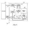
- FIG. 9illustrates a functional block diagram of a memory device 900 that can incorporate the vertical NAND architecture NROM memory array 700 or vertical NOR architecture NROM memory cell array 600 of the present invention.
- the memory device 900is coupled to a processor 910 .
- the processor 910may be a microprocessor or some other type of controlling circuitry.
- the memory device 900 and the processor 910form part of an electronic system 920 .
- the memory device 900has been simplified to focus on features of the memory that are helpful in understanding the present invention.
- the memory deviceincludes an array of vertical NROM memory cells and select gates 930 .
- the memory cellsare vertical NROM memory cells and the memory array 930 are arranged in banks of rows and columns.
- the control gates of each row of memory cellsis coupled with a wordline while the drain and source connections of the memory cells are coupled to bitlines.
- the connection of the cells to the bitlinesdepends on whether the array is a NAND architecture or a NOR architecture.
- An address buffer circuit 940is provided to latch address signals provided on address/data bus 962 . Address signals are received and decoded by a row decoder 944 and a column decoder 946 to access the memory array 930 . It will be appreciated by those skilled in the art, with the benefit of the present description, that the size of address input on the address/data bus 962 depends on the density and architecture of the memory array 930 . That is, the size of the input address increases with both increased memory cell counts and increased bank and block counts. It is noted that other address input manners, such as through a separate address bus, are also known and will be understood by those skilled in the art with the benefit of the present description.
- the memory device 900reads data in the memory array 930 by sensing voltage or current changes in the memory array columns using sense/buffer circuitry 950 .
- the sense/buffer circuitryin one embodiment, is coupled to read and latch a row of data from the memory array 930 .
- Data input and output buffer circuitry 960is included for bi-directional data communication over a plurality of data connections in the address/data bus 962 with the processor/controller 910 .
- Write circuitry 955is provided to write data to the memory array.
- Control circuitry 970decodes signals provided on control connections 972 from the processor 910 . These signals are used to control the operations on the memory array 930 , including data read, data write, and erase operations.
- the control circuitry 970may be a state machine, a sequencer, or some other type of controller.
- the memory device 900 of FIG. 9may be an embedded device with a CMOS processor.
- FIG. 9has been simplified to facilitate a basic understanding of the features of the memory. A more detailed understanding of internal circuitry and functions of memories are known to those skilled in the art.
- NROM EEPROM memory devices and arrayshave been described that facilitate the use of vertical NROM memory cells and select gates in NOR or NAND high density memory architectures.
- Memory embodiments of the present inventionutilize vertical select gates and NROM memory cells to form NOR and NAND NROM architecture memory cell strings, segments, and arrays.
- These NROM memory cell architecturesallow for improved high density memory devices or arrays with integral select gates that can take advantage of the feature sizes semiconductor fabrication processes are generally capable of and yet do not suffer from charge separation issues in typical multi-bit NROM cells.
- the memory cell architecturesalso allow for mitigation of disturb and overerasure issues by placing the NROM memory cells behind select gates that isolate the memory cells from their associated bit/data lines and/or source lines.
Landscapes
- Engineering & Computer Science (AREA)
- Chemical & Material Sciences (AREA)
- Nanotechnology (AREA)
- Physics & Mathematics (AREA)
- Mathematical Physics (AREA)
- Theoretical Computer Science (AREA)
- Crystallography & Structural Chemistry (AREA)
- Non-Volatile Memory (AREA)
- Semiconductor Memories (AREA)
Abstract
Description
- This application is related to U.S. application Ser. No. 10/769,116 (Attorney Docket No. 400.261US01) filed Jan. 30, 2004, entitled “VERTICAL DEVICE 4F2EEPROM MEMORY,” which is commonly assigned.
- The present invention relates generally to integrated circuits and in particular the present invention relates to EEPROM memory devices.
- Memory devices are typically provided as internal storage areas in the computer. The term memory identifies data storage that comes in the form of integrated circuit chips. There are several different types of memory used in modern electronics, one common type is RAM (random-access memory). RAM is characteristically found in use as main memory in a computer environment. RAM refers to read and write memory; that is, you can both write data into RAM and read data from RAM. This is in contrast to read-only memory (ROM), which permits you only to read data. Most RAM is volatile, which means that it requires a steady flow of electricity to maintain its contents. As soon as the power is turned off, whatever data was in RAM is lost.
- Computers almost always contain a small amount of ROM that holds instructions for starting up the computer. Unlike RAM, ROM cannot be written to. An EEPROM (electrically erasable programmable read-only memory) is a special type non-volatile ROM that can be erased by exposing it to an electrical charge. EEPROM comprise a large number of memory cells having electrically isolated gates (floating gates). Data is stored in the memory cells in the form of charge on the floating gates. Charge is transported to or removed from the floating gates by specialized programming and erase operations, respectively.
- Yet another type of non-volatile memory is a Flash memory. A Flash memory is a type of EEPROM that is typically erased and reprogrammed in blocks instead of one byte at a time. A typical Flash memory comprises a memory array, which includes a large number of memory cells. Each of the memory cells includes a floating gate field-effect transistor capable of holding a charge. The data in a cell is determined by the presence or absence of the charge in the floating gate. The cells are usually grouped into sections called “erase blocks.” The memory cells of a Flash memory array are typically arranged into a “NOR” architecture (each cell directly coupled to a bit line) or a “NAND” architecture (cells coupled into “strings” of cells, such that each cell is coupled indirectly to a bit line and requires activating the other cells of the string for access). Each of the cells within an erase block can be electrically programmed in a random basis by charging the floating gate. The charge can be removed from the floating gate by a block erase operation, wherein all floating gate memory cells in the erase block are erased in a single operation.
- One recent type of Flash memory is a nitride read only memory (NROM). NROM has some of the characteristics of Flash memory but does not require the special fabrication processes of a conventional Flash memory, thus NROM integrated circuits can be implemented using a standard CMOS process. Because of their unique device characteristics, some NROM memory cells can also store multiple data bits in each cell (typically two bits each).
FIG. 1 illustrates a cross-sectional view of a typical prior art NROM memory cell with a channel length, L. The cell is comprised of acontrol gate 100 formed on top of an oxide-nitride-oxide (ONO) layer. This layer is comprised of anoxide layer 101 on top of anitride 103 layer upon which the charge is stored for the various states of the cell. In one embodiment, the cell has trappingareas nitride layer 103. Thenitride layer 103 is deposited on anotheroxide layer 104 that is on the substrate.- Two source/
drain regions gate 100. The source/drain regions channel area 110 between the two source/drain regions drain region 109 or111 (i.e., whether source or drain) depends upon whichbit trapping area drain region 111 and output from theright side region 109, the left side is thesource 111 and the right side is thedrain 109 and the data bit charge is stored on thenitride 103 at thesource end 111 forbit trapping area 106. - As integrated circuit processing techniques improve, manufacturers try to reduce the feature sizes of the devices produced and thus increase the density of the IC circuits and memory arrays. In NROM memory arrays in particular, the channel length of the NROM memory cells that make up the memory array and spacing between memory cells in the strings have a large effect on the number of memory cells that can be placed in a given area and thus a direct impact on the density of the array and size of the resulting memory device. In addition, in many cases the feature sizes of the devices are limited by the device characteristics before the minimum feature size that the process is capable of is reached. In NROM devices in particular, as the channel length is reduced, a minimum size is typically reached that is primarily dictated by the device operational characteristics.
FIG. 2 illustrates a typical prior art planar NROM device that has a channel length that is less than 100 nm. In this case, the channel length is so short that thetrapping areas - A further problem in floating gate and NROM memory cell arrays is the issue of overerased memory cells. An NROM memory cell is structurally similar to a MOSFET transistor, with a control gate separated from a channel, source, and drain by an insulator. In addition, embedded in the insulator is an isolated trapping layer. As in a MOSFET transistor, current flows when the NROM memory cell/transistor is selected or activated, charge trapped on the trapping layer affects the amount of current flow in the NROM transistor, depending on its direction of operation (current flow in the channel), effectively raising or lowering its threshold in the direction of operation. In programming or erasing an NROM memory cell, charge is transported to or from the electrically insulated trapping layer of the NROM transistor. If too much charge is removed from the trapping layer of the NROM transistor/memory cell it will flow current in this direction of operation even when it is not selected. NROM transistors in this overerased state can affect current flow on shared bitlines and/or memory strings and thus potentially corrupt data read from other memory cells these common bitlines and/or memory strings.
- For the reasons stated above, and for other reasons stated below which will become apparent to those skilled in the art upon reading and understanding the present specification, there is a need in the art for a method and architecture for producing a more closely spaced and, thus, higher density NROM memory array without trapping area overlap and with improved overerasure handling properties.
- The above-mentioned problems with producing a more closely spaced and higher density NROM memory array with improved overerasure handling properties and other problems are addressed by the present invention and will be understood by reading and studying the following specification.
- NROM EEPROM memory devices and arrays, in accordance with embodiments of the present invention, facilitate the utilization of vertical NROM memory cells and select gates in NOR or NAND high density memory architectures. Memory embodiments of the present invention utilize vertical select gates and NROM memory cells to form NOR and NAND NROM architecture memory cell strings, segments, and arrays. These NROM memory cell architectures allow for an improved high density memory devices or arrays with integral select gates that can take advantage of the feature sizes semiconductor fabrication processes are generally capable of and yet do not suffer from charge separation issues in typical multi-bit NROM cells. The memory cell architectures also allow for mitigation of disturb and overerasure issues by placing the NROM memory cells behind select gates that isolate the memory cells from their associated bit/data lines.
- For one embodiment, the invention provides a memory device comprising a NOR architecture NROM memory array formed on a substrate having a plurality of pillars and associated intervening trenches. A plurality of memory cell structures, each memory cell structure comprising, an NROM memory cell is formed vertically on a first sidewall of a trench. A select gate is formed on a second sidewall of the trench. The select gate is coupled to the NROM memory cell by a first source/drain region formed at the bottom of the trench.
- For another embodiment, the invention provides an NROM memory cell structure comprising a substrate, having two raised areas, defining a trench therebetween. An NROM memory cell is formed vertically on a first sidewall of the trench, and a select gate memory cell is formed vertically on a second sidewall of the trench. The NROM memory cell is coupled to the select gate by source/drain regions at the bottom of the trench.
- For yet another embodiment, the invention provides a method of forming an NROM memory cell structure comprising forming two raised areas on a substrate, the raised areas defining an associated intervening trench. The method further includes forming an NROM memory cell on a first sidewall of the trench, forming a select gate on a second sidewall of the trench, and forming a source/drain region at the bottom of the associated intervening trench.
- For a further embodiment, the invention provides a NAND architecture NROM memory cell string comprising a substrate, comprising one or more raised areas, defining trenches therebetween. A plurality of NROM memory cells are formed vertically on the sidewalls of the trenches and are coupled in a serial string by source/drain regions formed at the top of the one or more raised areas and at the bottom of the one or more trenches. Additionally, a first NROM memory cell of the string is coupled to a first select gate.
- For yet a further embodiment, the invention provides a memory array comprising a substrate having a plurality of pillars and associated intervening trenches. A plurality of NROM memory cells are formed vertically on the sidewalls of the plurality of pillars and trenches, wherein the plurality of NROM memory cells are coupled into a plurality of NAND architecture memory strings by source/drain regions formed at the top of the plurality of pillars and at the bottom of the associated trenches. Additionally, a first NROM memory cell of each NAND architecture memory string is coupled to a first vertical select gate and a last NROM memory cell of each NAND architecture memory string is coupled to a second vertical select gate.
- For another embodiment, the invention provides a method of forming a NAND architecture memory cell string comprising forming one or more raised areas on a substrate, the raised areas defining associated intervening trenches. The method further includes forming a plurality of NROM memory cells on the sidewalls of the one or more raised areas, forming one or more source/drain regions on the top of the one or more raised areas and at the bottom of the one or more associated intervening trenches, and forming a first vertical select gate coupled to a first NROM memory cell of the string and a second vertical select gate coupled to a last NROM memory cell of the string.
- Other embodiments are also described and claimed.
FIG. 1 shows a cross-sectional view of a typical prior art NROM cell.FIG. 2 shows a cross-sectional view of a typical prior art NROM cell with a channel less than 100 nm.FIGS. 3A and 3B detail erase operations in NROM memory cells.FIGS. 4A-4C detail a planar NAND NROM memory array of the prior art.FIGS. 5A-5C detail a planar NOR NROM memory array of the prior art.FIGS. 6A-6C detail vertical NOR NROM memory array and cells in accordance with embodiments of the present invention.FIGS. 7A and 7B detail vertical NAND NROM memory array and cells in accordance with embodiments of the present invention.FIGS. 8A-8C detail formation of a vertical NAND architecture NROM memory array having NROM memory cells and select gates in accordance with embodiments of the present invention.FIG. 9 details a block diagram of an electronic system in accordance with embodiments of the present invention.- In the following detailed description of the preferred embodiments, reference is made to the accompanying drawings that form a part hereof, and in which is shown by way of illustration specific preferred embodiments in which the inventions may be practiced. These embodiments are described in sufficient detail to enable those skilled in the art to practice the invention, and it is to be understood that other embodiments may be utilized and that logical, mechanical and electrical changes may be made without departing from the spirit and scope of the present invention. The terms wafer and substrate used previously and in the following description include any base semiconductor structure. Both are to be understood as including silicon-on-sapphire (SOS) technology, silicon-on-insulator (SOI) technology, thin film transistor (TFT) technology, doped and undoped semiconductors, epitaxial layers of silicon supported by a base semiconductor, as well as other semiconductor structures well known to one skilled in the art. Furthermore, when reference is made to a wafer or substrate in the following description, previous process steps may have been utilized to form regions/junctions in the base semiconductor structure. The following detailed description is, therefore, not to be taken in a limiting sense, and the scope of the present invention is defined only by the claims and equivalents thereof.
- NROM EEPROM memory devices and arrays, in accordance with embodiments of the present invention, facilitate the utilization of vertical NROM memory cells and select gates in NOR or NAND high density memory architectures. Memory embodiments of the present invention utilize vertical select gates and NROM memory cells to form NOR and NAND NROM architecture memory cell strings, segments, and arrays. These NROM memory cell architectures allow for improved high density memory devices or arrays with integral select gates that can take advantage of the feature sizes semiconductor fabrication processes are generally capable of and yet do not suffer from charge separation issues in typical multi-bit NROM cells. By constructing NROM memory cells/gates in a vertical orientation, embodiments of the present invention allow for increases in memory array cell density and improved utilization of process minimum feature size capabilities while maintaining an appropriate NROM memory cell channel length to allow for effective charge separation. The memory cell architectures also allow for mitigation of disturb and overerasure issues by placing the NROM memory cells behind select gates that isolate the memory cells from their associated bit/data lines and/or source lines.
- As stated above, as integrated circuit processing techniques improve, manufacturers try to reduce the feature sizes of the devices produced and thus increase the density of the IC circuits and memory arrays. In many cases, the feature sizes of the devices are limited by the device characteristics before the minimum feature size that the process is capable of is reached. In both NAND and NOR architecture NROM EEPROM memory arrays, as the channel length is reduced and the spacing between memory cells in the strings are reduced, a minimum size is reached that is dictated by the operational characteristics of the NROM memory cell devices that make up the memory array. As a result, the maximum density of an array of memory cells is limited even if the process technology can attain even smaller features and/or channel lengths. In particular, this is an issue in higher capacity memory types where small changes in the memory cell footprint (e.g., memory cell channel widths) and the cell density in the array can have a large effect on the overall array size and the resulting storage capacity.
- As stated above, programming an NROM memory cell involves the insertion and storage of charge on the memory cell's trapping layer. However, as also stated above, because of their unique device characteristics, NROM memory cells can also store multiple data bits in each cell, storing a data bit in the trapping layer of the device near each source/drain region for two bits in a typical NROM memory cell transistor. In this, an NROM memory cell transistor is read and programmed in both a forwards and backwards direction of current flow in the source/drain regions (interchanging their source/drain function) to allow access to programming, reading, and erasing the two stored data bits. The function of each source/drain region (i.e., whether source or drain) depends upon which bit trapping area is being read or written. For example, in a read operation, if the carrier is input at the left side source/drain region and output from the right side region, the left side is the source and the right side is the drain and the data bit charge is stored on the nitride at the source end for bit trapping area. Because of the localized storage of electrons in the trapping layer, while reading the NROM memory cell only the charge stored in the trapping layer nearest the source/drain region operating as the source affects the current flow through the device. The charge stored near the other source/drain region is “read through” and has minimal influence. The bits in an NROM memory cell transistor are programmed in the reverse bias/current flow direction from the read direction for each stored data bit.
- Typically, an NROM memory cell electrically operates as an enhancement type MOS transistor, requiring a positive voltage applied across the gate and channel to flow current. The presence, or lack thereof, of a trapped charge on the trapping layer of the NROM transistor/memory cell near the source/drain region biased as the drain alters the threshold voltage characteristics of this transistor in this bias direction and thus the amount of current the transistor will flow at a given gate channel voltage. The effective threshold voltage of the NROM transistor memory cell in the selected bias direction increases with storage of electrons on the trapping layer near the source/drain region operating as the source and decreases with the removal of stored charge. Reading NROM memory cells in EEPROM memory arrays is then accomplished by accessing a memory cell with selected read voltage levels on the control gate and data/bit line coupled to the source/drain region biased as the source. The stored data is then typically sensed from the amount of current the NROM memory cell flows through the coupled bit/data line coupled to the source/drain region biased as the drain.
- In programming NROM memory cells in EEPROM memory arrays, electrons are typically transferred to the trapping layer of the memory cell by one of Fowler-Nordheim tunneling (FN-Tunneling) or channel hot electron injection (HEI). Other forms of programming NROM memory cells, such as, substrate enhanced hot electron injection (SEHE), are also known and utilized, but may not be appropriate for multi-bit operation. FN-Tunneling is typically accomplished by applying a positive control gate voltage on the NROM memory cell with respect to its channel to tunnel inject electrons to the trapping layer. Channel hot electron injection (HEI) is typically accomplished by applying a positive voltage on the control gate and the source/drain region biased as the drain of the NROM memory cell and a low voltage or ground on the source/drain region biased as the source to inject electrons to the trapping layer. In many cases the programming voltages are iteratively pulsed and the memory cell read to check the programming process and more accurately program the NROM memory cell.
- Erasure of the NROM memory cells of EEPROM memory arrays is typically accomplished by conventional tunneling or negative voltages applied to the control gate voltages with respect to the channel. Alternatively, other forms of erasure, such as, substrate enhanced band to band tunneling induced hot hole injection (SEBBHH) can also be used for NROM memory cell erasure, but again, may not by suitable for multi-bit operation. To ensure uniformity, in many cases the EEPROM memory programs all the NROM memory cells in the data segment to be erased before applying the voltages to erase the memory cells. As with programming, the erasure voltages are typically iteratively pulsed and the memory cells checked after each pulse to verify erasure and return of the NROM memory cells to an un-programmed threshold voltage state.
- Unfortunately, it is possible, during an erasure process, for too much charge to be removed from the trapping layer or individual trapping areas of an NROM memory cell transistor placing it in to an “overerased” state. In such cases, enough charge is removed that the threshold voltage of the NROM memory cell transistor is altered so that it operates as a depletion mode device, requiring a negative control gate-channel voltage to be applied to shut off current flow in the selected bias direction. In this state, the NROM memory cell transistor will flow a current even when it has not been selected by the memory, unless a negative voltage is applied to the control gate with respect to the source. This “overerased” state and the resulting current flow in the selected bias direction when the overerased NROM memory cell is unselected can interfere with attempts to read the values of other NROM memory cells that share the common bit lines with it, corrupting the read data.
- Complicating the issue of overerasure in NROM memory cells is that not all NROM memory cells erase (remove charge from their trapping layers or trapping areas) at the same rate of speed. Typically, one or more “fast erasing” memory cells will erase more quickly than the others of the group of cells selected for erasure. To minimize the possibility of inadvertently overerasing this group of fast erasing NROM memory cells most NROM EEPROM and Flash memory devices/arrays typically utilize the complex and time consuming iterative erase voltage pulse-memory cell verify process noted above to erase its NROM memory cells.
FIG. 3A details a chart of a distribution ofthreshold voltages 300 of NROM memory cells in a given array, showing distribution bell curves of the threshold voltages of NROM memory cells placed in a programmed302 and erased304 state in a given bias direction as may be typical of an NROM memory device.FIG. 3A also details a number of erased cells that have been inadvertently placed in an overerased (depletion mode)306 state.FIG. 3B details abit line 310 of amemory array 312 and thecurrent flow 314 through an overerasedNROM memory cell 316 that has not been selected/activated for reading.- An additional issue that can affect the memory cells of an EEPROM or Flash memory array is “disturb.” Disturb typically happens when the elevated voltages used to program or erase an NROM memory cell segment or erase block “disturb” the programmed values stored in other trapping areas of other NROM memory cells corrupting them and causing errors when they are later read. These inadvertently disturbed cells typically share common word lines, bit lines, or source lines with the memory cells that are being programmed or erased.
- By constructing their NROM memory cells vertically and isolating them with select gates, embodiments of the present invention allow for increases in memory array cell density and improved utilization of process minimum feature size capabilities, while maintaining the size of the memory cell channel to allow for appropriate device operation. In addition, by increasing the available surface area for transistors and incorporating select gates, which are also constructed in a vertical manner, embodiments of the present invention mitigate issues with overerasure and disturb, allowing for greater reliability and faster programming and erasure.
- As previously stated, the two common types of EEPROM and Flash memory array architectures are the “NAND” and “NOR” architectures, so called for the similarity each basic memory cell configuration has to the corresponding logic gate design. In the NOR array architecture, the NROM memory cells of the memory array are arranged in a matrix similar to RAM or ROM. The gates of each NROM memory cell of the array matrix are coupled by rows to word select lines (word lines) and their source/drain regions are coupled to column bit lines. The NOR architecture NROM memory array is accessed by a row decoder activating a row of NROM memory cells by selecting the word line coupled to their gates. The row of selected memory cells then place their stored data values on the column bit lines by flowing a differing current from the coupled source line to the coupled column bit lines depending on their programmed states. A column page of bit lines is selected and sensed, and individual data words are selected from the sensed data words from the column page and communicated from the memory.
- A NAND array architecture also arranges its array of NROM memory cells in a matrix such that the gates of each NROM memory cell of the array are coupled by rows to word lines. However each memory cell is not directly coupled to a source line and a column bit line. Instead, the memory cells of the array are arranged together in strings, typically of 8, 16, 32, or more each, where the memory cells in the string are coupled together in series, source to drain, between a common source line and a column bit line. This allows a NAND array architecture to have a higher memory cell density than a comparable NOR array, but with the cost of a generally slower access rate and programming complexity.
- A NAND architecture NROM memory array is accessed by a row decoder activating a row of NROM memory cells by selecting the word select line coupled to their gates. In addition, the word lines coupled to the gates of the unselected memory cells of each string are also driven. However, the unselected memory cells of each string are typically driven by a higher gate voltage so as to operate them as pass transistors and allowing them to pass current in a manner that is unrestricted by their stored data values. Current then flows from the source line to the column bit line through each NROM memory cell of the series coupled string, restricted only by the memory cells of each string that are selected to be read. This places the current encoded stored data values of the row of selected memory cells on the column bit lines. A column page of bit lines is selected and sensed, and then individual data words are selected from the sensed data words from the column page and communicated from the memory.
FIGS. 4A, 4B , and4C show a simplified planar NROM memory array of a EEPROM or Flash memory device of the prior art.FIG. 4A details a top view of a planar NOR architectureNROM memory array 400, a side view of the planarNROM memory array 400 is detailed inFIG. 4B . InFIGS. 4A, 4B , and4C,NROM memory cells 402 are coupled together in a NOR architecture memory array havingbit lines 412 and word lines406. The bit/source lines 412 are formed locally from N+ doped regions deposited in thesubstrate 408. EachNROM memory cell 402 has a gate-insulator stack formed between the N+ doped regions of abit line 412, utilizing the N+ doped regions as a drain and source respectively. The gate-insulator stack is made of an insulator on top of asubstrate 408, a trapping layer formed on the insulator, an intergate insulator formed over the trapping layer, and a control gate406 (typically formed integral to theword line 406, also known as a control gate line) formed over the intergate insulator.FIG. 4C details anequivalent circuit schematic 420 of the NOR architectureNROM memory array 400, showingNROM memory cells 402 coupled to the bit lines, word lines, andsubstrate connection 422.FIGS. 5A, 5B , and5C show a simplified planar NAND NROM memory array of a EEPROM or Flash memory device of the prior art.FIG. 5A details a top view of a planar NANDNROM memory string 504 of a NAND architectureNROM memory array 500, a side view of the planar NANDNROM memory string 504 is detailed inFIG. 5B . InFIGS. 5A and 5B , a series ofNROM memory cells 502 are coupled together in a series NAND string504 (typically of 8, 16, 32, or more cells). EachNROM memory cell 502 has a gate-insulator stack that is made of an insulator on top of asubstrate 508, a trapping layer formed on the insulator, an intergate insulator formed over the trapping layer, and a control gate506 (typically formed in a control gate line, also known as a word line) formed over the intergate insulator. N+ doped regions are formed between each gate insulator stack to form the source/drain regions of the adjacent NROM memory cells, which additionally operate as connectors to couple the cells of theNAND string 504 together.Select gates 510, that are coupled to gate select lines, are formed at either end of theNAND NROM string 504 and selectively couple opposite ends of theNAND NROM string 504 to abit line contacts 512.FIG. 5C details anequivalent circuit schematic 520 of the NAND architectureNROM memory string 504, showingNROM memory cells 502 andsubstrate connection 522.- Embodiments of the present invention utilize vertical NROM memory cells and vertical gate structures. Methods of forming vertical memory cells are detailed in U.S. patent application Ser. No. 10/177,208, titled “Vertical NROM having a storage density of 1 bit per 1F2”, filed Jun. 21, 2002, and U.S. Pat. No. 5,936,274, titled “High density flash memory”, issued Aug. 10, 1999, which are commonly assigned. Methods of forming vertical split control gates are detailed U.S. Pat. No. 6,150,687, titled “Memory cell having a vertical transistor with buried source/drain and dual gates”, issued Nov. 21, 2000, and U.S. Pat. No. 6,072,209, titled “Four F2folded bit line DRAM cell structure having buried bit and word lines”, issued Jun. 6, 2000, which are also commonly assigned.
FIGS. 6A-6C detail vertical NROM memory cells and select gates for a NOR architecture NROM memory array in accordance with embodiments of the present invention.FIG. 6A details a side view of a simplified vertical NOR architecturememory cell structure 604, a side view of a vertical NORmemory array 600 is detailed inFIG. 6B .FIG. 6C details anequivalent circuit schematic 620 of the vertical NOR architectureNROM memory array 600, showingNROM memory cells 602 andsubstrate connection 622. It is noted that the NOR architectureNROM memory array 600 can be utilized in both EEPROM or Flash memories arrays and devices. As can be seen fromFIGS. 6A and 6B , in a single vertical NOR architecturememory cell structure 604, two vertically formed transistors occupy the area that a single planar NROM transistor would occupy (an area of 4F squared when viewed from above, each transistor having an area of 2F squared). Where “F” is the minimum resolvable photolithographic dimension in the particular process technology.- In
FIG. 6A , a vertically formedNROM memory cell 602 andselect gate 610 are coupled together in series in a vertical NOR architecturememory cell structure 604. In creating the vertical NOR architecture memory cell structure604 atrench 630 is formed in asubstrate 608. The verticalNROM memory cell 602 andselect gate 610 are then formed on the sidewalls of thetrench 630. The verticalNROM memory cell 602 has a gate-insulator stack made of aninsulator 620 formed on the surface of the sidewall, a trapping layer622 (typically of nitride) formed on theinsulator 620, anintergate insulator 624 formed over theNROM 622, and a control gate606 (typically formed in a control gate line, also known as a word line) formed over theintergate insulator 624. In one embodiment, thesubstrate trench 630 is formed by patterning a masking material that is layered over thesubstrate 608 and anisotropically etching thetrenches 630. The gate-insulator stack of theNROM memory cell 602 is formed in one embodiment by successive layering of each of the materials of the gate insulator stack over thetrench 630, followed by a mask and directional etch of the deposit of each layer to leave only the material deposited on the sidewall of thetrench 630. In another embodiment, differing layers of the gate-insulator stack are formed and then masked and directionally etched in a single step. - The vertical
select gate 610 has a gate-insulator stack made of aninsulator 642 formed on the opposite sidewall of thetrench 630 with acontrol gate 644 formed over theinsulator 642. The gate-insulator stack of theselect gate 610 is formed by successive layering of each of the materials of the gate insulator stack over thetrench 630, as with the verticalNROM memory cell 602, but skips the depositing of theinsulator 620 andtrapping layer 622 layers. In one embodiment of the present invention theinsulator 620 and thetrapping layer 622 of theNROM memory cell 602 are formed and then theintergate insulator 624/control gate 606 of theNROM memory cell 602 and theinsulator 642/control gate 644 of theselect gate 610 are formed consecutively. - N+ doped
regions 626 are formed at the raised areas at the top and at the bottom of thetrenches 630 to form the source/drain regions for the vertical NROM memory cell/gate-insulator stack 602 andselect gate 610. The N+ regions also couple thememory cell 602 andselect gate 610 together to form the vertical NORmemory structure 604 and additionally couple the vertical NOR architecturememory cell structure 604 to the bit lines612. It is noted that the N+ source/drain regions 626 may be formed before or after the formation of theNROM memory cell 602 andselect gate 610 gate-insulator stacks. - In
FIG. 6B , a vertical NOR architectureNROM memory array 600 is formed from a series of vertical NOR architecturememory cell structures 604. Each vertical NOR architecturememory cell structures 604 having a vertically formedNROM memory cell 602 and a coupledselect gate 610, wherein the drain of the select gate is coupled to a first bit/data line 612 and a source/drain of theNROM 602 is coupled to a second bit/data line 612. - In creating the vertical NOR architecture NROM memory array600 a series of
substrate pillars 628 are formed in asubstrate 608 withtrenches 630 located between them. The verticalNROM memory cells 602 andselect gates 610 are then formed on the sidewalls of thepillars 628 within thetrenches 630 to form the vertical NOR architecturememory cell structures 604. The verticalNROM memory cells 602 andselect gates 610 are formed in an alternating pattern (NROM-select gate, select gate-NROM, NROM-select gate, etc.) such that eachpillar 628 has eitherselect gates 610 or NROM memory cells formed on its sidewalls. - N+ doped
regions 626 are formed at the top of thepillars 628 and at the bottom of thetrenches 630 to form the source and drain regions. The N+ regions at the bottom of thetrenches 630 couple thememory cell 602 andselect gate 610 of each vertical NOR architecturememory cell structure 604 together. The N+ regions at the tops of thepillars 628 couple the drain of theselect gate 610 and the source of theNROM memory cell 602 of each vertical NOR architecturememory cell structure 604 to thebit lines 612 respectively. It is again noted that the N+ source/drain regions 626 may be formed before or after the formation of theNROM memory cell 602 andselect gate 610 gate-insulator stacks. - It is also noted that isolation regions, typically formed of an oxide insulator, can be used between adjacent rows of vertical NOR architecture
memory cell structures 604 to isolate each row from its neighbors. These isolation regions can be extended into thesubstrate 608 to allow the formation of P-wells, where each P-well contains a single row of vertical NOR architecturememory cell structures 604 that can be biased in isolation from the other rows of thearray 600. It is also noted that the control gate/word address lines 606 andselect lines 640 can cross these isolation regions so that each control gate/word address line 606 andselect line 640 controls the operation of multipleNROM memory cells 602 andselect gates 610, respectively, across multiple rows of vertical NOR architecturememory cell structures 604. - As stated above,
FIG. 6C details anequivalent circuit schematic 620 of the vertical NOR architectureNROM memory array 600, showingNROM memory cells 602 andsubstrate connection 622. The verticalNROM memory cells 602 andselect gates 610 are formed in an alternating pattern (NROM-select gate, select gate-NROM, NROM-select gate, etc.) so that the drain of theselect gate 610 and the source/drain of theNROM memory cell 602 of adjacent vertical NOR architecturememory cell structures 604 are both coupled to asingle bit line 612. It is noted that non-alternating patterns are also possible. It is noted that other array patterns of verticalNROM memory cells 602,select gates 610, and vertical NROMmemory cell structures 604 are possible and will be apparent to those skilled in the art with the benefit of the present disclosure. - In the vertical NOR architecture
NROM memory array 600 ofFIGS. 6A-6C , the channel length of eachNROM memory cell 602 andselect gate 610 in a vertical NOR architecturememory cell structure 604 is determined by the depth of thetrenches 630 and not by the minimum feature size. Due to the vertical form of the vertical NOR architectureNROM memory array 600 and vertical NOR architecturememory cell structures 604 of embodiments of the present invention, a NOR architecture NROM memory array can be produced that contain a verticalNROM memory cell 602 that does not suffer from charge separation issues and a coupledselect gate 610 in the space that would be utilized by a single conventional planar NROM memory cell. - The addition of a
select gate 610 coupled between thebit line 612 and a source/drain of eachNROM memory cell 602 allows for theNROM memory cell 602 to be isolated from thebit lines 612 and thus has advantages in both programming and erasing theNROM memory cells 602 of the vertical NOR architectureNROM memory array 600. In erasing, the coupledselect gate 610 allows for avoidance of overerasure issues withNROM memory cells 602 by isolating eachmemory cell 602 behind aselect gate 610 so that, even if anNROM memory cell 602 is overerased into depletion mode, it will not corrupt the reading ofother memory cells 602 on its coupledbit lines 612 by flowing current. As the possibility of corruption of data reads due to overerasure is mitigated, this allows for the NOR architectureNROM memory array 600 to speed up its erasure processes by using larger erase pulses (in time or voltage) or even utilizing only a single erase pulse. In addition, by allowing the increase of erasure pulse time and voltage, the number of erasure verifications required are reduced or even eliminated. The coupledselect gate 610 also allows for the isolated erasure of one or moreNROM memory cells 602 allowing erasure of individualNROM memory cells 602, one or more selected data words, data segments, or erase blocks. - In programming, the coupled
select gate 610 allows for mitigation of programming disturb ofNROM memory cells 602 in thearray 600 by theselect gate 610 isolating or buffering thememory cells 602 from the bit lines612. This allows for longer and higher voltage programming pulses to be used without increasing the possibility of disturb issues. FIGS. 7A-7D detail vertical NROM cells, vertical select gates, and NAND architecture NROM memory strings in accordance with embodiments of the present invention.FIG. 7A details a side view of a simplified vertical NAND architectureNROM memory string 704 with verticalselect gates 710.FIG. 7B details an equivalent circuit schematic720 of the vertical NAND architectureNROM memory string 704, showingNROM memory cells 702 andsubstrate connection 734.FIG. 7C details a side view of a simplified vertical NAND architectureNROM memory array 700 andFIG. 7D details an equivalent circuit schematic of one embodiment of the present invention. Again, as can be seen fromFIGS. 7A and 7C , in a vertical NANDarchitecture memory string 704, two vertically formed transistors occupy the area that each planar transistor would occupy (an area of 4F squared when viewed from above, each transistor having an area of 2F squared). Where “F” is the minimum resolvable photolithographic dimension in the particular process technology. Since each transistor can store a single bit of data the data storage density is one bit for each 2F squared unit area. Thus, for example, if F=0.1 micron then the storage density is 0.5 Giga bit per square centimeter.- In
FIG. 7A , a series of vertically formedNROM memory cells 702 are coupled together in a series NROM NAND string704 (typically of 8, 16, 32, or more cells). In the vertical NAND NROMmemory array string 704 ofFIGS. 7A-7D , a series ofsubstrate pillars 728 are formed in asubstrate 708 withtrenches 730 located between them. The verticalNROM memory cells 702 are then formed on the sidewalls of thepillars 728 within thetrenches 730. Each verticalNROM memory cell 702 is formed on the sidewalls of the substrate pillars728 (for twoNROM memory cells 702 per trench730) and has a gate-insulator stack made of an insulator720 formed on the surface of the sidewall, a trapping layer722 (typically of polysilicon) formed on the insulator720, anintergate insulator 724 formed over thetrapping layer 722, and a control gate706 (typically formed in a control gate line, also known as a word line) formed over theintergate insulator 724. - In one embodiment the
substrate pillars 728 andtrenches 730 are formed by patterning a masking material that is layered over thesubstrate 708 and anisotropically etching thetrenches 730. The gate-insulator stack of eachNROM memory cell 702 are formed in one embodiment by successive layering of each of the materials of the gate insulator stack over thepillars 728 andtrenches 730, followed by a mask and directional etch of the deposit of each layer to leave only the material deposited on the sidewall of thepillars 728. In another embodiment, differing layers of the gate-insulator stack are formed and then masked and directionally etched in a single step. - N+ doped
regions 726 are formed at the top of thesubstrate pillars 728 and at the bottom of thetrenches 730 between each vertical NROM memory cell/gate-insulator stack 702 to form the source and drain regions of the adjacentNROM memory cells 702 and couple thememory cells 702 together to form the vertical NANDarchitecture memory string 704. It is noted that the N+ source/drain regions 726 may be formed before or after the formation of the NROM memory cells/gate-insulator stack 702. Select gates 710, that are coupled to gate select lines, are formed at either end of the NANDNROM memory string 704 and selectively couple opposite ends of the NANDNROM memory string 704 to abit line contacts 712. The verticalselect gates 710 have a gate-insulator stack made of aninsulator 742 formed on a sidewall with acontrol gate 744 formed over theinsulator 742. The gate-insulator stack of theselect gates 710 are formed by successive layering of each of the materials of the gate insulator stack over thepillars 728 andtrenches 730, as with the verticalNROM memory cell 702, but skips the depositing of the insulator720 andtrapping layer 722 layers. TheN+ regions 726 also couple the first andlast memory cell 702 of the vertical NANDarchitecture NROM string 704 to theselect gates 710 and additionally couple the vertical NANDarchitecture NROM string 704 to the bit lines712.- As stated above,
FIG. 7B details an equivalent circuit schematic of the vertical NAND architectureNROM memory array 700, showing the verticalNROM memory cells 702,select gates 710,bit line 712 connections, andsubstrate connection 734, in accordance with embodiments of the present invention. As can be seen, the schematic provides the same equivalent circuit as that of a conventional planar NAND architecture NROM memory string. - In
FIG. 7C , a section of vertical NAND architectureNROM memory array 700 of one embodiment of the present invention is formed from a series of vertical NAND architecture NROM memory cell strings704. InFIG. 7C , each pair of adjacent vertical NAND architecture NROM memory cell strings704 in the vertical NAND architectureNROM memory array 700 are coupled through verticalselect gates 710 to acommon bit line 712 by a N+ dopedregion 726 formed at the top of apillar 728. - It is also noted that isolation regions, typically formed of an oxide insulator, can be used between vertical NAND architecture NROM memory cell strings704 to isolate each
string 704 from its neighbors. These isolation regions can be extended into thesubstrate 708 to allow the formation of P-wells, where each P-well contains a single vertical NAND architecture NROMmemory cell string 704 that can be biased in isolation from the other strings or rows of thearray 700. It is also noted that the control gate/word address lines 706 andselect lines 740 can cross these isolation regions so that each control gate/word address line 706 andselect line 740 controls the operation ofNROM memory cells 702 andselect gates 710 respectively across multiple rows of vertical NAND architecture NROM memory cell strings704. - As stated above,
FIG. 7D details an equivalent circuit schematic of the vertical NAND architecture NROM memory array ofFIG. 7C , showingNROM memory cells 702 andadjacent sting 704 connection. - In the vertical NAND architecture
NROM memory array 700 ofFIGS. 7A-7D , the channel length of eachNROM memory cell 702 andselect gate 710 in a vertical NANDarchitecture memory string 704 is determined by the depth of thepillars 728 andtrenches 730 and not by the minimum feature size. Due to the vertical form of the NAND architectureNROM memory array 700 and NANDarchitecture memory strings 704 of embodiments of the present invention, a vertical NAND architecture NROMmemory array string 704 andselect gates 710 can be produced that typically has twice the density for a given string horizontal run length than a corresponding planar NAND architecture NROM memory array string. - The addition of
select gates 710 coupled between thebit lines 712 and theNROM memory cells 702 of the vertical NANDarchitecture memory string 704 allows for theNROM memory cells 702 of the vertical NANDarchitecture memory string 704 to be isolated from one or both of thebit lines 712 and thus has advantages in both programming and erasing the vertical NANDarchitecture memory string 704. In erasing, the coupledselect gates 710 allows for avoidance of overerasure issues withNROM memory cells 702 by isolating each vertical NANDarchitecture memory string 704 behind one or moreselect gates 710 so that even if theNROM memory cells 702 of the vertical NANDarchitecture memory string 704 are overerased into depletion mode operation they will not corrupt the reading ofother memory cells 702 on other vertical NANDarchitecture memory strings 704 that are coupled to thesame bit line 712. As the possibility of corruption of data reads due to overerasure is mitigated, this allows for the vertical NAND architectureNROM memory array 700 to speed up erasure processes by using larger erase pulses or even a single erase pulse and by reducing or eliminating erasure verification. The coupledselect gates 710 also allow for the isolated erasure of one or moreNROM memory cells 702 allowing erasure of individualNROM memory cells 702, individual vertical NANDarchitecture memory strings 704, one or more selected data words, or erase blocks. In programming, the coupledselect gates 710 allow for mitigation of programming disturb ofNROM memory cells 702 in thearray 700 by theselect gates 710 isolating thememory cells 702 of the vertical NANDarchitecture memory strings 704 from the bit lines712. This allows for longer and higher voltage programming pulses to be used without an increased issue with of disturb problems. FIGS. 8A-8C detail three dimensional views ofvertical NROM cells 802 and verticalselect gates 810 of a vertical NANDNROM memory array 800 in accordance with embodiments of the present invention at several mid-fabrication stages. It is noted that a formation process that is similar to the NAND process may be utilized for formation of a vertical NORNROM memory array 600 with the exception of placement and number of theselect gates 810 and bit line and source line contacts. As stated above, in creating the vertical NANDNROM memory array 800, a series ofsubstrate pillars 828 are formed in asubstrate 808 withtrenches 830 located between them. The verticalNROM memory cells 802 andselect gates 810 are then formed on the sidewalls of thepillars 828 within thetrenches 830. Between successive rows ofsubstrate pillars 828,isolation regions 832 have been formed on the faces of thepillars 828 that are not utilized to formNROM memory cells 802 orselect gates 810 to isolate each row of vertical NAND NROM memory strings804 from the neighboring rows. Theseisolation regions 832 are typically formed of an oxide insulator.- As stated above, in creating each NROM memory cell gate-
insulator stack 802, aninsulator 820 is formed on the surface of the sidewall, atrapping layer 822 is formed on theinsulator 820, anintergate insulator 824 is formed over thetrapping layer 822, and acontrol gate 806 is formed over theintergate insulator 824. In creating each select gate gate-insulator stack 810, aninsulator 842 is formed on the surface of the sidewall, and acontrol gate 844 is formed over theinsulator 842. - In
FIG. 8A , thetrenches 830 have been already formed by masking and anisotropically/directionally etching thetrenches 830 in thesubstrate 808. N+ dopedregions 826 have been formed at the top of theunformed substrate pillars 828 and at the bottom of thetrenches 830 to form the source/drain regions of theNROM memory cells 802. The gate-insulator stack of eachNROM memory cell 802 have been partially formed on the sidewalls of thetrenches 830. In eachtrench 830, with the exception of thepillar 828 on which theselect gates 810 are to be formed, are formed theinsulator 820, thetrapping layer 822, and theintergate insulator 824, by successive depositing, masking, and directional etching of layers of material. - In
FIG. 8B , thepillars 828 are formed and the space between each pillar in successive rows of NAND architecture NROM memory strings804 are filled with an oxide to formisolation regions 832. In forming thepillars 828, the rows of NAND architecture NROM memory strings804 are masked and directionally etched. This masking and etching process also divides the NROM layer into individual trapping layers822. - In
FIG. 8C , the control gates/word lines 806 andselect gates 810/select lines 840 are formed. In forming the control gates/word lines 806 andselect gates 810/select lines 840, successive layers of insulator and polysilicon which will form the control gates/word lines 806 andselect gates 810/select lines 840 is deposited over thepillars 828,trenches 830, and partially formed gate-insulator stacks of theNROM memory cells 802 of thememory array 800. A layer of masking material is then formed over the polysilicon layer and patterned. The excess masking material is removed and thememory array 800 is anisotropically/directionally etched to remove the undesired portions of the deposited polysilicon and form the control gates/word lines 806 andselect gates 810/select lines 840 on the sidewalls of thepillars 828 andtrenches 830. - It is noted that the
isolation regions 832 between the vertical NANDarchitecture NROM strings 804 can be extended into thesubstrate 808 to allow the formation of P-wells, where each P-well contains asingle NAND string 804 and can be biased in isolation from theother strings 804 of thearray 800. It is also noted that the control gates/word lines 806 andselect gates 810/select lines 840 cross theseisolation regions 832 so that each control gate/word address line 806 controls the operation ofNROM memory cells 802 and eachselect line 840 the operation ofselect gates 810 across multiple NAND memory strings804. - In
FIGS. 8A-8C , thesubstrate 808 of the vertical NAND architectureNROM memory array 800 is P-doped. A substrate connection can be utilized that can allow for biasing of the P-dopedsubstrate 808. It is noted that other forms of substrate doping, substrate biasing, and substrate types and regions (including, but not limited to silicon-on-sapphire (SOS) technology, silicon-on-insulator (SOI) technology, thin film transistor (TFT) technology, doped and undoped semiconductors, epitaxial layers of silicon supported by a base semiconductor) in embodiments of the present invention are possible and should be apparent to those skilled in the art with the benefit of the present invention. - It is noted that the NROM memory cells of embodiments of the present invention can be formed from multiple conventional materials. For the gate-insulator stack (gate insulator-trapping layer-top insulator) these materials may include, but are not limited to, oxide-nitride-oxide (ONO), oxide-nitride-aluminum oxide, oxide-aluminum oxide-oxide, oxide-silicon oxycarbide-oxide, composite layers of a silicon oxide-an oxide of Ti, Ta, Hf, Zr, or La, and a silicon oxide, and composite layers of an oxide-a non-stoichiometric oxide of Si, N, Al, Ti, Ta, Hf, Zr, and La, and an oxide. Additional trapping layer materials for NROM memory cell embodiments of the present invention, may also include, but are not limited to, wet oxides not annealed, silicon rich oxides, silicon rich aluminum oxide, silicon oxycarbide, silicon oxide with silicon carbide nanoparticles, and non-stoichiometric oxides of Si, N, Al, Ti, Ta, Hf, Zr, and La.
- As noted above the programming of the NROM memory cells of the vertical NAND and NOR NROM architecture memory structures, strings, and arrays of embodiments of the present invention can be accomplished by conventional tunnel injection of electrons by having a positive gate voltage with respect to the substrate or P-well. In another embodiment of the present invention, programming is accomplished by channel hot electron injection (HEI). Erasure of the NROM memory cells of embodiments of the present invention can accomplished by conventional tunneling or negative voltages applied to the control gate voltages with respect to the substrate or P-well. With the above listed programming and erasure techniques, the NROM memory cells of embodiments of the present invention can be utilized for two-bit storage as a conventional planar NROM memory cells would be, storing charge in the trapping layer near each source/drain, allowing one bit to be read/programmed when biased in the forward direction and the other to be read/programmed when biased in the reverse direction.
- In alternative embodiments of the present invention, substrate enhanced hot electron injection (SEHE) can be utilized for NROM memory cell programming and/or substrate enhanced band to band tunneling induced hot hole injection (SEBBHH) for NROM memory cell erasure. However, while the required voltages for these operations may be lower, they may only be suitable for single bit storage operation mode.
FIG. 9 illustrates a functional block diagram of amemory device 900 that can incorporate the vertical NAND architectureNROM memory array 700 or vertical NOR architecture NROMmemory cell array 600 of the present invention. Thememory device 900 is coupled to aprocessor 910. Theprocessor 910 may be a microprocessor or some other type of controlling circuitry. Thememory device 900 and theprocessor 910 form part of anelectronic system 920. Thememory device 900 has been simplified to focus on features of the memory that are helpful in understanding the present invention.- The memory device includes an array of vertical NROM memory cells and
select gates 930. In one embodiment, the memory cells are vertical NROM memory cells and thememory array 930 are arranged in banks of rows and columns. The control gates of each row of memory cells is coupled with a wordline while the drain and source connections of the memory cells are coupled to bitlines. As is well known in the art, the connection of the cells to the bitlines depends on whether the array is a NAND architecture or a NOR architecture. - An
address buffer circuit 940 is provided to latch address signals provided on address/data bus 962. Address signals are received and decoded by arow decoder 944 and acolumn decoder 946 to access thememory array 930. It will be appreciated by those skilled in the art, with the benefit of the present description, that the size of address input on the address/data bus 962 depends on the density and architecture of thememory array 930. That is, the size of the input address increases with both increased memory cell counts and increased bank and block counts. It is noted that other address input manners, such as through a separate address bus, are also known and will be understood by those skilled in the art with the benefit of the present description. - The
memory device 900 reads data in thememory array 930 by sensing voltage or current changes in the memory array columns using sense/buffer circuitry 950. The sense/buffer circuitry, in one embodiment, is coupled to read and latch a row of data from thememory array 930. Data input andoutput buffer circuitry 960 is included for bi-directional data communication over a plurality of data connections in the address/data bus 962 with the processor/controller 910. Writecircuitry 955 is provided to write data to the memory array. Control circuitry 970 decodes signals provided oncontrol connections 972 from theprocessor 910. These signals are used to control the operations on thememory array 930, including data read, data write, and erase operations. Thecontrol circuitry 970 may be a state machine, a sequencer, or some other type of controller.- Since the vertical NROM memory cells of the present invention use a CMOS compatible process, the
memory device 900 ofFIG. 9 may be an embedded device with a CMOS processor. - The memory device illustrated in
FIG. 9 has been simplified to facilitate a basic understanding of the features of the memory. A more detailed understanding of internal circuitry and functions of memories are known to those skilled in the art. - It is also noted that other vertical NAND and NOR architecture NROM memory strings, segments, arrays, and memory devices in accordance with embodiments of the present invention are possible and should be apparent to those skilled in the art with benefit of the present disclosure.
- NROM EEPROM memory devices and arrays have been described that facilitate the use of vertical NROM memory cells and select gates in NOR or NAND high density memory architectures. Memory embodiments of the present invention utilize vertical select gates and NROM memory cells to form NOR and NAND NROM architecture memory cell strings, segments, and arrays. These NROM memory cell architectures allow for improved high density memory devices or arrays with integral select gates that can take advantage of the feature sizes semiconductor fabrication processes are generally capable of and yet do not suffer from charge separation issues in typical multi-bit NROM cells. The memory cell architectures also allow for mitigation of disturb and overerasure issues by placing the NROM memory cells behind select gates that isolate the memory cells from their associated bit/data lines and/or source lines.
- Although specific embodiments have been illustrated and described herein, it will be appreciated by those of ordinary skill in the art that any arrangement, which is calculated to achieve the same purpose, may be substituted for the specific embodiment shown. This application is intended to cover any adaptations or variations of the present invention. Therefore, it is manifestly intended that this invention be limited only by the claims and the equivalents thereof.
Claims (71)
Priority Applications (9)
| Application Number | Priority Date | Filing Date | Title |
|---|---|---|---|
| US10/785,310US7075146B2 (en) | 2004-02-24 | 2004-02-24 | 4F2 EEPROM NROM memory arrays with vertical devices |
| KR1020067019550AKR100847409B1 (en) | 2004-02-24 | 2005-02-16 | Vertical eeprom nrom memory devices |
| EP05723109AEP1719170A1 (en) | 2004-02-24 | 2005-02-16 | Vertical eeprom nrom memory devices |
| CNA2005800115413ACN1943028A (en) | 2004-02-24 | 2005-02-16 | Vertical EEPROM NROM memory device |
| PCT/US2005/004815WO2005083782A1 (en) | 2004-02-24 | 2005-02-16 | Vertical eeprom nrom memory devices |
| KR1020087012089AKR20080053531A (en) | 2004-02-24 | 2005-02-16 | NRM memory cell structure and method for forming same, NAD architecture NRM memory cell string and method for forming same |
| JP2007500877AJP2007523502A (en) | 2004-02-24 | 2005-02-16 | Vertical EEPROM NROM memory device |
| TW094104780ATWI278988B (en) | 2004-02-24 | 2005-02-18 | 4F2 EEPROM NROM memory arrays with vertical devices |
| US11/192,472US7282762B2 (en) | 2004-02-24 | 2005-07-29 | 4F2 EEPROM NROM memory arrays with vertical devices |
Applications Claiming Priority (1)
| Application Number | Priority Date | Filing Date | Title |
|---|---|---|---|
| US10/785,310US7075146B2 (en) | 2004-02-24 | 2004-02-24 | 4F2 EEPROM NROM memory arrays with vertical devices |
Related Child Applications (1)
| Application Number | Title | Priority Date | Filing Date |
|---|---|---|---|
| US11/192,472DivisionUS7282762B2 (en) | 2004-02-24 | 2005-07-29 | 4F2 EEPROM NROM memory arrays with vertical devices |
Publications (2)
| Publication Number | Publication Date |
|---|---|
| US20050184337A1true US20050184337A1 (en) | 2005-08-25 |
| US7075146B2 US7075146B2 (en) | 2006-07-11 |
Family
ID=34861601
Family Applications (2)
| Application Number | Title | Priority Date | Filing Date |
|---|---|---|---|
| US10/785,310Expired - Fee RelatedUS7075146B2 (en) | 2004-02-24 | 2004-02-24 | 4F2 EEPROM NROM memory arrays with vertical devices |
| US11/192,472Expired - LifetimeUS7282762B2 (en) | 2004-02-24 | 2005-07-29 | 4F2 EEPROM NROM memory arrays with vertical devices |
Family Applications After (1)
| Application Number | Title | Priority Date | Filing Date |
|---|---|---|---|
| US11/192,472Expired - LifetimeUS7282762B2 (en) | 2004-02-24 | 2005-07-29 | 4F2 EEPROM NROM memory arrays with vertical devices |
Country Status (7)
| Country | Link |
|---|---|
| US (2) | US7075146B2 (en) |
| EP (1) | EP1719170A1 (en) |
| JP (1) | JP2007523502A (en) |
| KR (2) | KR20080053531A (en) |
| CN (1) | CN1943028A (en) |
| TW (1) | TWI278988B (en) |
| WO (1) | WO2005083782A1 (en) |
Cited By (14)
| Publication number | Priority date | Publication date | Assignee | Title |
|---|---|---|---|---|
| US20040232472A1 (en)* | 2000-03-28 | 2004-11-25 | Kabushhiki Kaisha Toshiba | Nonvolatile semiconductor memory and method of manufacturing the same |
| US7167398B1 (en)* | 2005-02-23 | 2007-01-23 | Spansion L.L.C. | System and method for erasing a memory cell |
| US20070228451A1 (en)* | 2006-03-30 | 2007-10-04 | Catalyst Semiconductor, Inc. | Scalable Electrically Eraseable And Programmable Memory (EEPROM) Cell Array |
| US7339239B2 (en) | 2003-12-17 | 2008-03-04 | Micron Technology, Inc. | Vertical NROM NAND flash memory array |
| US20080054336A1 (en)* | 2006-09-05 | 2008-03-06 | Georgescu Sorin S | Scalable Electrically Eraseable And Programmable Memory |
| US20080101124A1 (en)* | 2006-10-31 | 2008-05-01 | Atmel Corporation | Programming pulse generator |
| US20080101133A1 (en)* | 2006-10-31 | 2008-05-01 | Atmel Corporation | Adaptive gate voltage regulation |
| US20080165582A1 (en)* | 2006-09-05 | 2008-07-10 | Catalyst Semiconductor, Inc. | Scalable Electrically Eraseable And Programmable Memory |
| US20090003074A1 (en)* | 2006-03-30 | 2009-01-01 | Catalyst Semiconductor, Inc. | Scalable Electrically Eraseable And Programmable Memory (EEPROM) Cell Array |
| US7719046B2 (en) | 2003-07-01 | 2010-05-18 | Micron Technology, Inc. | Apparatus and method for trench transistor memory having different gate dielectric thickness |
| US8750041B2 (en) | 2006-09-05 | 2014-06-10 | Semiconductor Components Industries, Llc | Scalable electrically erasable and programmable memory |
| US20160351621A1 (en)* | 2006-09-21 | 2016-12-01 | Kabushiki Kaisha Toshiba | Semiconductor memory and method of manufacturing the same |
| US20170287566A1 (en)* | 2016-03-31 | 2017-10-05 | Sandisk Technologies Llc | Nand structure with tier select gate transistors |
| US11502128B2 (en) | 2020-06-18 | 2022-11-15 | Taiwan Semiconductor Manufacturing Company, Ltd. | Memory device and method of forming the same |
Families Citing this family (37)
| Publication number | Priority date | Publication date | Assignee | Title |
|---|---|---|---|---|
| US6878991B1 (en)* | 2004-01-30 | 2005-04-12 | Micron Technology, Inc. | Vertical device 4F2 EEPROM memory |
| US7190616B2 (en)* | 2004-07-19 | 2007-03-13 | Micron Technology, Inc. | In-service reconfigurable DRAM and flash memory device |
| US7158410B2 (en)* | 2004-08-27 | 2007-01-02 | Micron Technology, Inc. | Integrated DRAM-NVRAM multi-level memory |
| US7378707B2 (en)* | 2005-05-26 | 2008-05-27 | Micron Technology, Inc. | Scalable high density non-volatile memory cells in a contactless memory array |
| US7927948B2 (en) | 2005-07-20 | 2011-04-19 | Micron Technology, Inc. | Devices with nanocrystals and methods of formation |
| US7482619B2 (en)* | 2005-09-07 | 2009-01-27 | Samsung Electronics Co., Ltd. | Charge trap memory device comprising composite of nanoparticles and method of fabricating the charge trap memory device |
| US7692961B2 (en)* | 2006-02-21 | 2010-04-06 | Saifun Semiconductors Ltd. | Method, circuit and device for disturb-control of programming nonvolatile memory cells by hot-hole injection (HHI) and by channel hot-electron (CHE) injection |
| US20070247910A1 (en)* | 2006-04-20 | 2007-10-25 | Micron Technology, Inc. | NAND erase block size trimming apparatus and method |
| US20080042185A1 (en)* | 2006-08-15 | 2008-02-21 | Atmel Corporation | Eeprom memory array having 5f2 cells |
| US7961511B2 (en)* | 2006-09-26 | 2011-06-14 | Sandisk Corporation | Hybrid programming methods and systems for non-volatile memory storage elements |
| US7898848B2 (en)* | 2007-04-23 | 2011-03-01 | Intel Corporation | Memory including bipolar junction transistor select devices |
| US7492636B2 (en)* | 2007-04-27 | 2009-02-17 | Macronix International Co., Ltd. | Methods for conducting double-side-biasing operations of NAND memory arrays |
| US8367506B2 (en) | 2007-06-04 | 2013-02-05 | Micron Technology, Inc. | High-k dielectrics with gold nano-particles |
| US7749838B2 (en)* | 2007-07-06 | 2010-07-06 | Macronix International Co., Ltd. | Fabricating method of non-volatile memory cell |
| US8320191B2 (en) | 2007-08-30 | 2012-11-27 | Infineon Technologies Ag | Memory cell arrangement, method for controlling a memory cell, memory array and electronic device |
| US7981745B2 (en)* | 2007-08-30 | 2011-07-19 | Spansion Llc | Sacrificial nitride and gate replacement |
| US7684245B2 (en)* | 2007-10-30 | 2010-03-23 | Atmel Corporation | Non-volatile memory array architecture with joined word lines |
| JP2009163782A (en)* | 2007-12-13 | 2009-07-23 | Toshiba Corp | Semiconductor memory device |
| US7995392B2 (en) | 2007-12-13 | 2011-08-09 | Kabushiki Kaisha Toshiba | Semiconductor memory device capable of shortening erase time |
| KR20100004772A (en)* | 2008-07-04 | 2010-01-13 | 삼성전자주식회사 | Semiconductor device and method of operating the same |
| US8072803B2 (en) | 2009-05-26 | 2011-12-06 | Macronix International Co., Ltd. | Memory device and methods for fabricating and operating the same |
| US8320181B2 (en)* | 2009-08-25 | 2012-11-27 | Micron Technology, Inc. | 3D memory devices decoding and routing systems and methods |
| KR101576957B1 (en)* | 2009-10-22 | 2015-12-14 | 삼성전자주식회사 | Vertical semiconductor device, memory device, and manufacturing method thereof |
| US9608119B2 (en) | 2010-03-02 | 2017-03-28 | Micron Technology, Inc. | Semiconductor-metal-on-insulator structures, methods of forming such structures, and semiconductor devices including such structures |
| US9646869B2 (en) | 2010-03-02 | 2017-05-09 | Micron Technology, Inc. | Semiconductor devices including a diode structure over a conductive strap and methods of forming such semiconductor devices |
| US8507966B2 (en)* | 2010-03-02 | 2013-08-13 | Micron Technology, Inc. | Semiconductor cells, arrays, devices and systems having a buried conductive line and methods for forming the same |
| US8288795B2 (en)* | 2010-03-02 | 2012-10-16 | Micron Technology, Inc. | Thyristor based memory cells, devices and systems including the same and methods for forming the same |
| US8513722B2 (en) | 2010-03-02 | 2013-08-20 | Micron Technology, Inc. | Floating body cell structures, devices including same, and methods for forming same |
| US8254173B2 (en) | 2010-08-31 | 2012-08-28 | Micron Technology, Inc. | NAND memory constructions |
| US8598621B2 (en) | 2011-02-11 | 2013-12-03 | Micron Technology, Inc. | Memory cells, memory arrays, methods of forming memory cells, and methods of forming a shared doped semiconductor region of a vertically oriented thyristor and a vertically oriented access transistor |
| US8952418B2 (en) | 2011-03-01 | 2015-02-10 | Micron Technology, Inc. | Gated bipolar junction transistors |
| US8519431B2 (en) | 2011-03-08 | 2013-08-27 | Micron Technology, Inc. | Thyristors |
| US8772848B2 (en) | 2011-07-26 | 2014-07-08 | Micron Technology, Inc. | Circuit structures, memory circuitry, and methods |
| CN104143552B (en)* | 2013-05-07 | 2018-02-06 | 北京兆易创新科技股份有限公司 | A kind of electronics trapping memory cells |
| KR102271008B1 (en) | 2017-10-27 | 2021-06-29 | 삼성전자주식회사 | Semiconductor device |
| KR102574322B1 (en) | 2018-06-27 | 2023-09-05 | 삼성전자주식회사 | Semiconductor devices |
| US10559337B1 (en)* | 2018-11-30 | 2020-02-11 | Micron Technology, Inc. | Vertical decoder |
Citations (93)
| Publication number | Priority date | Publication date | Assignee | Title |
|---|---|---|---|---|
| US4184207A (en)* | 1978-01-27 | 1980-01-15 | Texas Instruments Incorporated | High density floating gate electrically programmable ROM |
| US4755864A (en)* | 1984-12-25 | 1988-07-05 | Kabushiki Kaisha Toshiba | Semiconductor read only memory device with selectively present mask layer |
| US5241496A (en)* | 1991-08-19 | 1993-08-31 | Micron Technology, Inc. | Array of read-only memory cells, eacch of which has a one-time, voltage-programmable antifuse element constructed within a trench shared by a pair of cells |
| US5330930A (en)* | 1992-12-31 | 1994-07-19 | Chartered Semiconductor Manufacturing Pte Ltd. | Formation of vertical polysilicon resistor having a nitride sidewall for small static RAM cell |
| US5378647A (en)* | 1993-10-25 | 1995-01-03 | United Microelectronics Corporation | Method of making a bottom gate mask ROM device |
| US5379253A (en)* | 1992-06-01 | 1995-01-03 | National Semiconductor Corporation | High density EEPROM cell array with novel programming scheme and method of manufacture |
| US5397725A (en)* | 1993-10-28 | 1995-03-14 | National Semiconductor Corporation | Method of controlling oxide thinning in an EPROM or flash memory array |
| US5620913A (en)* | 1996-05-28 | 1997-04-15 | Chartered Semiconductor Manufacturing Pte Ltd. | Method of making a flash memory cell |
| US5768192A (en)* | 1996-07-23 | 1998-06-16 | Saifun Semiconductors, Ltd. | Non-volatile semiconductor memory cell utilizing asymmetrical charge trapping |
| US5792697A (en)* | 1997-01-07 | 1998-08-11 | United Microelectronics Corporation | Method for fabricating a multi-stage ROM |
| US5858841A (en)* | 1997-01-20 | 1999-01-12 | United Microelectronics Corporation | ROM device having memory units arranged in three dimensions, and a method of making the same |
| US5888868A (en)* | 1996-01-22 | 1999-03-30 | Semiconductor Energy Laboratory Co., Ltd. | Method for fabricating EPROM device |
| US5909618A (en)* | 1997-07-08 | 1999-06-01 | Micron Technology, Inc. | Method of making memory cell with vertical transistor and buried word and body lines |
| US5911106A (en)* | 1996-08-29 | 1999-06-08 | Nec Corporation | Semiconductor memory device and fabrication thereof |
| US5936274A (en)* | 1997-07-08 | 1999-08-10 | Micron Technology, Inc. | High density flash memory |
| US5946558A (en)* | 1997-02-05 | 1999-08-31 | United Microelectronics Corp. | Method of making ROM components |
| US6011725A (en)* | 1997-08-01 | 2000-01-04 | Saifun Semiconductors, Ltd. | Two bit non-volatile electrically erasable and programmable semiconductor memory cell utilizing asymmetrical charge trapping |
| US6028342A (en)* | 1996-11-22 | 2000-02-22 | United Microelectronics Corp. | ROM diode and a method of making the same |
| US6030871A (en)* | 1998-05-05 | 2000-02-29 | Saifun Semiconductors Ltd. | Process for producing two bit ROM cell utilizing angled implant |
| US6044022A (en)* | 1999-02-26 | 2000-03-28 | Tower Semiconductor Ltd. | Programmable configuration for EEPROMS including 2-bit non-volatile memory cell arrays |
| US6072209A (en)* | 1997-07-08 | 2000-06-06 | Micro Technology, Inc. | Four F2 folded bit line DRAM cell structure having buried bit and word lines |
| US6081456A (en)* | 1999-02-04 | 2000-06-27 | Tower Semiconductor Ltd. | Bit line control circuit for a memory array using 2-bit non-volatile memory cells |
| US6091102A (en)* | 1996-05-16 | 2000-07-18 | Altera Corporation | High-density nonvolatile memory cell |
| US6108240A (en)* | 1999-02-04 | 2000-08-22 | Tower Semiconductor Ltd. | Implementation of EEPROM using intermediate gate voltage to avoid disturb conditions |
| US6172396B1 (en)* | 1998-02-03 | 2001-01-09 | Worldwide Semiconductor Manufacturing Corp. | ROM structure and method of manufacture |
| US6174758B1 (en)* | 1999-03-03 | 2001-01-16 | Tower Semiconductor Ltd. | Semiconductor chip having fieldless array with salicide gates and methods for making same |
| US6175523B1 (en)* | 1999-10-25 | 2001-01-16 | Advanced Micro Devices, Inc | Precharging mechanism and method for NAND-based flash memory devices |
| US6181597B1 (en)* | 1999-02-04 | 2001-01-30 | Tower Semiconductor Ltd. | EEPROM array using 2-bit non-volatile memory cells with serial read operations |
| US6184089B1 (en)* | 1999-01-27 | 2001-02-06 | United Microelectronics Corp. | Method of fabricating one-time programmable read only memory |
| US6191470B1 (en)* | 1997-07-08 | 2001-02-20 | Micron Technology, Inc. | Semiconductor-on-insulator memory cell with buried word and body lines |
| US6201737B1 (en)* | 2000-01-28 | 2001-03-13 | Advanced Micro Devices, Inc. | Apparatus and method to characterize the threshold distribution in an NROM virtual ground array |
| US6204529B1 (en)* | 1999-08-27 | 2001-03-20 | Hsing Lan Lung | 8 bit per cell non-volatile semiconductor memory structure utilizing trench technology and dielectric floating gate |
| US6207504B1 (en)* | 1998-07-29 | 2001-03-27 | United Semiconductor Corp. | Method of fabricating flash erasable programmable read only memory |
| US6208557B1 (en)* | 1999-05-21 | 2001-03-27 | National Semiconductor Corporation | EPROM and flash memory cells with source-side injection and a gate dielectric that traps hot electrons during programming |
| US6208164B1 (en)* | 1998-08-04 | 2001-03-27 | Micron Technology, Inc. | Programmable logic array with vertical transistors |
| US6215702B1 (en)* | 2000-02-16 | 2001-04-10 | Advanced Micro Devices, Inc. | Method of maintaining constant erasing speeds for non-volatile memory cells |
| US6218695B1 (en)* | 1999-06-28 | 2001-04-17 | Tower Semiconductor Ltd. | Area efficient column select circuitry for 2-bit non-volatile memory cells |
| US6219299B1 (en)* | 2000-05-31 | 2001-04-17 | Micron Technology, Inc. | Programmable memory decode circuits with transistors with vertical gates |
| US6222769B1 (en)* | 1997-06-06 | 2001-04-24 | Kabushiki Kaisha Toshiba | Nonvolatile semiconductor storage device having buried electrode within shallow trench |
| US6222768B1 (en)* | 2000-01-28 | 2001-04-24 | Advanced Micro Devices, Inc. | Auto adjusting window placement scheme for an NROM virtual ground array |
| US20010001075A1 (en)* | 1997-03-25 | 2001-05-10 | Vantis Corporation | Process for fabricating semiconductor memory device with high data retention including silicon nitride etch stop layer formed at high temperature with low hydrogen ion concentration |
| US6238976B1 (en)* | 1997-07-08 | 2001-05-29 | Micron Technology, Inc. | Method for forming high density flash memory |
| US6240020B1 (en)* | 1999-10-25 | 2001-05-29 | Advanced Micro Devices | Method of bitline shielding in conjunction with a precharging scheme for nand-based flash memory devices |
| US6243300B1 (en)* | 2000-02-16 | 2001-06-05 | Advanced Micro Devices, Inc. | Substrate hole injection for neutralizing spillover charge generated during programming of a non-volatile memory cell |
| US6249460B1 (en)* | 2000-02-28 | 2001-06-19 | Micron Technology, Inc. | Dynamic flash memory cells with ultrathin tunnel oxides |
| US20010004332A1 (en)* | 1998-05-20 | 2001-06-21 | Saifun Semiconductors Ltd. | NROM cell with improved programming, erasing and cycling |
| US6251731B1 (en)* | 1998-08-10 | 2001-06-26 | Acer Semiconductor Manufacturing, Inc. | Method for fabricating high-density and high-speed nand-type mask roms |
| US6255166B1 (en)* | 1999-08-05 | 2001-07-03 | Aalo Lsi Design & Device Technology, Inc. | Nonvolatile memory cell, method of programming the same and nonvolatile memory array |
| US6256231B1 (en)* | 1999-02-04 | 2001-07-03 | Tower Semiconductor Ltd. | EEPROM array using 2-bit non-volatile memory cells and method of implementing same |
| US6266281B1 (en)* | 2000-02-16 | 2001-07-24 | Advanced Micro Devices, Inc. | Method of erasing non-volatile memory cells |
| US6269023B1 (en)* | 2000-05-19 | 2001-07-31 | Advanced Micro Devices, Inc. | Method of programming a non-volatile memory cell using a current limiter |
| US6272043B1 (en)* | 2000-01-28 | 2001-08-07 | Advanced Micro Devices, Inc. | Apparatus and method of direct current sensing from source side in a virtual ground array |
| US6275414B1 (en)* | 2000-05-16 | 2001-08-14 | Advanced Micro Devices, Inc. | Uniform bitline strapping of a non-volatile memory cell |
| US6282118B1 (en)* | 2000-10-06 | 2001-08-28 | Macronix International Co. Ltd. | Nonvolatile semiconductor memory device |
| US6337808B1 (en)* | 1999-08-30 | 2002-01-08 | Micron Technology, Inc. | Memory circuit and method of using same |
| US6348711B1 (en)* | 1998-05-20 | 2002-02-19 | Saifun Semiconductors Ltd. | NROM cell with self-aligned programming and erasure areas |
| US6377070B1 (en)* | 2001-02-09 | 2002-04-23 | Micron Technology, Inc. | In-service programmable logic arrays with ultra thin vertical body transistors |
| US6380585B1 (en)* | 1997-12-30 | 2002-04-30 | Matsushita Electric Industrial Co., Ltd. | Nonvolatile semiconductor device capable of increased electron injection efficiency |
| US6384448B1 (en)* | 2000-02-28 | 2002-05-07 | Micron Technology, Inc. | P-channel dynamic flash memory cells with ultrathin tunnel oxides |
| US6383871B1 (en)* | 1999-08-31 | 2002-05-07 | Micron Technology, Inc. | Method of forming multiple oxide thicknesses for merged memory and logic applications |
| US6392930B2 (en)* | 2000-02-14 | 2002-05-21 | United Microelectronics Corp. | Method of manufacturing mask read-only memory cell |
| US6417053B1 (en)* | 2001-11-20 | 2002-07-09 | Macronix International Co., Ltd. | Fabrication method for a silicon nitride read-only memory |
| US6417049B1 (en)* | 2000-02-01 | 2002-07-09 | Taiwan Semiconductor Manufacturing Company | Split gate flash cell for multiple storage |
| US6421275B1 (en)* | 2002-01-22 | 2002-07-16 | Macronix International Co. Ltd. | Method for adjusting a reference current of a flash nitride read only memory (NROM) and device thereof |
| US6424001B1 (en)* | 2001-02-09 | 2002-07-23 | Micron Technology, Inc. | Flash memory with ultra thin vertical body transistors |
| US6429063B1 (en)* | 1999-10-26 | 2002-08-06 | Saifun Semiconductors Ltd. | NROM cell with generally decoupled primary and secondary injection |
| US6432778B1 (en)* | 2001-08-07 | 2002-08-13 | Macronix International Co. Ltd. | Method of forming a system on chip (SOC) with nitride read only memory (NROM) |
| US6514831B1 (en)* | 2001-11-14 | 2003-02-04 | Macronix International Co., Ltd. | Nitride read only memory cell |
| US20030042512A1 (en)* | 2001-08-30 | 2003-03-06 | Micron Technology, Inc. | Vertical transistor and method of making |
| US20030043637A1 (en)* | 2001-08-30 | 2003-03-06 | Micron Technology, Inc | Flash memory with low tunnel barrier interpoly insulators |
| US6531887B2 (en)* | 2001-06-01 | 2003-03-11 | Macronix International Co., Ltd. | One cell programmable switch using non-volatile cell |
| US6545309B1 (en)* | 2002-03-11 | 2003-04-08 | Macronix International Co., Ltd. | Nitride read-only memory with protective diode and operating method thereof |
| US20030067807A1 (en)* | 2001-09-28 | 2003-04-10 | Hung-Sui Lin | Erasing method for p-channel NROM |
| US6552287B2 (en)* | 1999-10-08 | 2003-04-22 | Itt Manufacturing Enterprises, Inc. | Electrical switch with snap action dome shaped tripper |
| US6552387B1 (en)* | 1997-07-30 | 2003-04-22 | Saifun Semiconductors Ltd. | Non-volatile electrically erasable and programmable semiconductor memory cell utilizing asymmetrical charge trapping |
| US6559013B1 (en)* | 2002-06-20 | 2003-05-06 | Macronix International Co., Ltd. | Method for fabricating mask ROM device |
| US6566682B2 (en)* | 2001-02-09 | 2003-05-20 | Micron Technology, Inc. | Programmable memory address and decode circuits with ultra thin vertical body transistors |
| US6577533B2 (en)* | 2000-03-28 | 2003-06-10 | Kabushiki Kaisha Toshiba | Nonvolatile semiconductor memory and method of manufacturing the same |
| US6576511B2 (en)* | 2001-05-02 | 2003-06-10 | Macronix International Co., Ltd. | Method for forming nitride read only memory |
| US6580135B2 (en)* | 2001-06-18 | 2003-06-17 | Macronix International Co., Ltd. | Silicon nitride read only memory structure and method of programming and erasure |
| US6580630B1 (en)* | 2002-04-02 | 2003-06-17 | Macronix International Co., Ltd. | Initialization method of P-type silicon nitride read only memory |
| US20030113969A1 (en)* | 2001-12-18 | 2003-06-19 | Samsung Electronics Co.,Ltd. | Method of forming flash memory |
| US20030117861A1 (en)* | 2001-12-20 | 2003-06-26 | Eduardo Maayan | NROM NOR array |
| US20030130356A1 (en)* | 2001-10-16 | 2003-07-10 | Slil Biomedical Corporation | Oligoamine compounds and derivatives thereof for cancer therapy |
| US20030134478A1 (en)* | 2002-01-16 | 2003-07-17 | Han-Chao Lai | Non-volatile memory and fabrication thereof |
| US6597037B1 (en)* | 1998-02-27 | 2003-07-22 | Micron Technology, Inc. | Programmable memory address decode array with vertical transistors |
| US6680508B1 (en)* | 2002-08-28 | 2004-01-20 | Micron Technology, Inc. | Vertical floating gate transistor |
| US20040016953A1 (en)* | 2002-07-26 | 2004-01-29 | Micron Technology, Inc. | Three dimensional flash cell |
| US20040041203A1 (en)* | 2000-05-25 | 2004-03-04 | Hynix Semiconductor Inc. | Non-volatile semiconductor memory device and fabricating method thereof |
| US20040063283A1 (en)* | 1996-02-28 | 2004-04-01 | Guterman Daniel C. | Eeprom with split gate source side injection |
| US6744094B2 (en)* | 2001-08-24 | 2004-06-01 | Micron Technology Inc. | Floating gate transistor with horizontal gate layers stacked next to vertical body |
| US6768162B1 (en)* | 2003-08-05 | 2004-07-27 | Powerchip Semiconductor Corp. | Split gate flash memory cell and manufacturing method thereof |
| US20050032308A1 (en)* | 2003-08-08 | 2005-02-10 | Ching-Nan Hsiao | Multi-bit vertical memory cell and method of fabricating the same |
Family Cites Families (53)
| Publication number | Priority date | Publication date | Assignee | Title |
|---|---|---|---|---|
| US4420504A (en) | 1980-12-22 | 1983-12-13 | Raytheon Company | Programmable read only memory |
| US4558344A (en) | 1982-01-29 | 1985-12-10 | Seeq Technology, Inc. | Electrically-programmable and electrically-erasable MOS memory device |
| US4785199A (en) | 1983-11-28 | 1988-11-15 | Stanford University | Programmable complementary transistors |
| JPS60182174A (en) | 1984-02-28 | 1985-09-17 | Nec Corp | Non-volatile semiconductor memory |
| JPS60220139A (en) | 1984-04-13 | 1985-11-02 | Fuji Electric Corp Res & Dev Ltd | Reaction induction method using light |
| US4774556A (en) | 1985-07-25 | 1988-09-27 | Nippondenso Co., Ltd. | Non-volatile semiconductor memory device |
| US4881114A (en) | 1986-05-16 | 1989-11-14 | Actel Corporation | Selectively formable vertical diode circuit element |
| US5146426A (en) | 1990-11-08 | 1992-09-08 | North American Philips Corp. | Electrically erasable and programmable read only memory with trench structure |
| JPH05251711A (en) | 1991-10-04 | 1993-09-28 | Oki Electric Ind Co Ltd | Semiconductor integrated circuit and its manufacture |
| US5461249A (en) | 1991-10-31 | 1995-10-24 | Rohm Co., Ltd. | Nonvolatile semiconductor memory device and manufacturing method therefor |
| US5467305A (en) | 1992-03-12 | 1995-11-14 | International Business Machines Corporation | Three-dimensional direct-write EEPROM arrays and fabrication methods |
| JP2877642B2 (en) | 1992-12-25 | 1999-03-31 | ローム株式会社 | Semiconductor memory device and driving method thereof |
| US5429967A (en) | 1994-04-08 | 1995-07-04 | United Microelectronics Corporation | Process for producing a very high density mask ROM |
| US5576236A (en) | 1995-06-28 | 1996-11-19 | United Microelectronics Corporation | Process for coding and code marking read-only memory |
| KR0170707B1 (en)* | 1995-11-29 | 1999-03-30 | 김광호 | Non-volatile memory device and its driving method |
| US5966603A (en) | 1997-06-11 | 1999-10-12 | Saifun Semiconductors Ltd. | NROM fabrication method with a periphery portion |
| US6297096B1 (en) | 1997-06-11 | 2001-10-02 | Saifun Semiconductors Ltd. | NROM fabrication method |
| US6150687A (en) | 1997-07-08 | 2000-11-21 | Micron Technology, Inc. | Memory cell having a vertical transistor with buried source/drain and dual gates |
| US5973352A (en) | 1997-08-20 | 1999-10-26 | Micron Technology, Inc. | Ultra high density flash memory having vertically stacked devices |
| US6133102A (en) | 1998-06-19 | 2000-10-17 | Wu; Shye-Lin | Method of fabricating double poly-gate high density multi-state flat mask ROM cells |
| US6134175A (en) | 1998-08-04 | 2000-10-17 | Micron Technology, Inc. | Memory address decode array with vertical transistors |
| US6157570A (en) | 1999-02-04 | 2000-12-05 | Tower Semiconductor Ltd. | Program/erase endurance of EEPROM memory cells |
| US6134156A (en) | 1999-02-04 | 2000-10-17 | Saifun Semiconductors Ltd. | Method for initiating a retrieval procedure in virtual ground arrays |
| US6147904A (en) | 1999-02-04 | 2000-11-14 | Tower Semiconductor Ltd. | Redundancy method and structure for 2-bit non-volatile memory cells |
| US6487050B1 (en) | 1999-02-22 | 2002-11-26 | Seagate Technology Llc | Disc drive with wear-resistant ramp coating of carbon nitride or metal nitride |
| US6303436B1 (en) | 1999-09-21 | 2001-10-16 | Mosel Vitelic, Inc. | Method for fabricating a type of trench mask ROM cell |
| US6291854B1 (en) | 1999-12-30 | 2001-09-18 | United Microelectronics Corp. | Electrically erasable and programmable read only memory device and manufacturing therefor |
| US6204126B1 (en) | 2000-02-18 | 2001-03-20 | Taiwan Semiconductor Manufacturing Company | Method to fabricate a new structure with multi-self-aligned for split-gate flash |
| US6436764B1 (en) | 2000-06-08 | 2002-08-20 | United Microelectronics Corp. | Method for manufacturing a flash memory with split gate cells |
| EP1172856A1 (en) | 2000-07-03 | 2002-01-16 | Matsushita Electric Industrial Co., Ltd. | Nonvolatile semiconductor memory device and method for fabricating the same |
| TW469601B (en) | 2000-12-08 | 2001-12-21 | Ememory Technology Inc | Dual bit trench type gate non-volatile flash memory cell structure and the operating method thereof |
| US6602805B2 (en) | 2000-12-14 | 2003-08-05 | Macronix International Co., Ltd. | Method for forming gate dielectric layer in NROM |
| JP3966707B2 (en) | 2001-02-06 | 2007-08-29 | 株式会社東芝 | Semiconductor device and manufacturing method thereof |
| US6496034B2 (en) | 2001-02-09 | 2002-12-17 | Micron Technology, Inc. | Programmable logic arrays with ultra thin body transistors |
| US6448601B1 (en) | 2001-02-09 | 2002-09-10 | Micron Technology, Inc. | Memory address and decode circuits with ultra thin body transistors |
| US6461949B1 (en) | 2001-03-29 | 2002-10-08 | Macronix International Co. Ltd. | Method for fabricating a nitride read-only-memory (NROM) |
| TW480677B (en) | 2001-04-04 | 2002-03-21 | Macronix Int Co Ltd | Method of fabricating a nitride read only memory cell |
| TW480678B (en) | 2001-04-13 | 2002-03-21 | Macronix Int Co Ltd | Method for producing nitride read only memory (NROM) |
| TW494541B (en) | 2001-05-28 | 2002-07-11 | Macronix Int Co Ltd | Method for producing silicon nitride read-only-memory |
| US20020182829A1 (en) | 2001-05-31 | 2002-12-05 | Chia-Hsing Chen | Method for forming nitride read only memory with indium pocket region |
| TW495974B (en) | 2001-06-21 | 2002-07-21 | Macronix Int Co Ltd | Manufacturing method for nitride read only memory |
| EP1271652A3 (en)* | 2001-06-22 | 2004-05-06 | Fujio Masuoka | A semiconductor memory and its production process |
| US6617204B2 (en) | 2001-08-13 | 2003-09-09 | Macronix International Co., Ltd. | Method of forming the protective film to prevent nitride read only memory cell charging |
| TW507369B (en) | 2001-10-29 | 2002-10-21 | Macronix Int Co Ltd | Silicon nitride read only memory structure for preventing antenna effect |
| US6486028B1 (en) | 2001-11-20 | 2002-11-26 | Macronix International Co., Ltd. | Method of fabricating a nitride read-only-memory cell vertical structure |
| US6498377B1 (en) | 2002-03-21 | 2002-12-24 | Macronix International, Co., Ltd. | SONOS component having high dielectric property |
| JP2003332469A (en)* | 2002-05-10 | 2003-11-21 | Fujitsu Ltd | Nonvolatile semiconductor memory device and method of manufacturing the same |
| US6853587B2 (en) | 2002-06-21 | 2005-02-08 | Micron Technology, Inc. | Vertical NROM having a storage density of 1 bit per 1F2 |
| US6996009B2 (en) | 2002-06-21 | 2006-02-07 | Micron Technology, Inc. | NOR flash memory cell with high storage density |
| US20030235076A1 (en) | 2002-06-21 | 2003-12-25 | Micron Technology, Inc. | Multistate NROM having a storage density much greater than 1 Bit per 1F2 |
| US6607957B1 (en) | 2002-07-31 | 2003-08-19 | Macronix International Co., Ltd. | Method for fabricating nitride read only memory |
| US6657250B1 (en) | 2002-08-21 | 2003-12-02 | Micron Technology, Inc. | Vertical flash memory cell with buried source rail |
| US6610586B1 (en) | 2002-09-04 | 2003-08-26 | Macronix International Co., Ltd. | Method for fabricating nitride read-only memory |
- 2004
- 2004-02-24USUS10/785,310patent/US7075146B2/ennot_activeExpired - Fee Related
- 2005
- 2005-02-16WOPCT/US2005/004815patent/WO2005083782A1/enactiveApplication Filing
- 2005-02-16JPJP2007500877Apatent/JP2007523502A/ennot_activeWithdrawn
- 2005-02-16KRKR1020087012089Apatent/KR20080053531A/ennot_activeCeased
- 2005-02-16CNCNA2005800115413Apatent/CN1943028A/enactivePending
- 2005-02-16KRKR1020067019550Apatent/KR100847409B1/ennot_activeExpired - Lifetime
- 2005-02-16EPEP05723109Apatent/EP1719170A1/ennot_activeWithdrawn
- 2005-02-18TWTW094104780Apatent/TWI278988B/ennot_activeIP Right Cessation
- 2005-07-29USUS11/192,472patent/US7282762B2/ennot_activeExpired - Lifetime
Patent Citations (99)
| Publication number | Priority date | Publication date | Assignee | Title |
|---|---|---|---|---|
| US4184207A (en)* | 1978-01-27 | 1980-01-15 | Texas Instruments Incorporated | High density floating gate electrically programmable ROM |
| US4755864A (en)* | 1984-12-25 | 1988-07-05 | Kabushiki Kaisha Toshiba | Semiconductor read only memory device with selectively present mask layer |
| US5241496A (en)* | 1991-08-19 | 1993-08-31 | Micron Technology, Inc. | Array of read-only memory cells, eacch of which has a one-time, voltage-programmable antifuse element constructed within a trench shared by a pair of cells |
| US5379253A (en)* | 1992-06-01 | 1995-01-03 | National Semiconductor Corporation | High density EEPROM cell array with novel programming scheme and method of manufacture |
| US5330930A (en)* | 1992-12-31 | 1994-07-19 | Chartered Semiconductor Manufacturing Pte Ltd. | Formation of vertical polysilicon resistor having a nitride sidewall for small static RAM cell |
| US5378647A (en)* | 1993-10-25 | 1995-01-03 | United Microelectronics Corporation | Method of making a bottom gate mask ROM device |
| US5397725A (en)* | 1993-10-28 | 1995-03-14 | National Semiconductor Corporation | Method of controlling oxide thinning in an EPROM or flash memory array |
| US5888868A (en)* | 1996-01-22 | 1999-03-30 | Semiconductor Energy Laboratory Co., Ltd. | Method for fabricating EPROM device |
| US20040063283A1 (en)* | 1996-02-28 | 2004-04-01 | Guterman Daniel C. | Eeprom with split gate source side injection |
| US6091102A (en)* | 1996-05-16 | 2000-07-18 | Altera Corporation | High-density nonvolatile memory cell |
| US5620913A (en)* | 1996-05-28 | 1997-04-15 | Chartered Semiconductor Manufacturing Pte Ltd. | Method of making a flash memory cell |
| US5768192A (en)* | 1996-07-23 | 1998-06-16 | Saifun Semiconductors, Ltd. | Non-volatile semiconductor memory cell utilizing asymmetrical charge trapping |
| US5911106A (en)* | 1996-08-29 | 1999-06-08 | Nec Corporation | Semiconductor memory device and fabrication thereof |
| US20010011755A1 (en)* | 1996-08-29 | 2001-08-09 | Kazuhiro Tasaka | Semiconductor memory device and fabrication thereof |
| US6028342A (en)* | 1996-11-22 | 2000-02-22 | United Microelectronics Corp. | ROM diode and a method of making the same |
| US5792697A (en)* | 1997-01-07 | 1998-08-11 | United Microelectronics Corporation | Method for fabricating a multi-stage ROM |
| US5858841A (en)* | 1997-01-20 | 1999-01-12 | United Microelectronics Corporation | ROM device having memory units arranged in three dimensions, and a method of making the same |
| US5946558A (en)* | 1997-02-05 | 1999-08-31 | United Microelectronics Corp. | Method of making ROM components |
| US20010001075A1 (en)* | 1997-03-25 | 2001-05-10 | Vantis Corporation | Process for fabricating semiconductor memory device with high data retention including silicon nitride etch stop layer formed at high temperature with low hydrogen ion concentration |
| US6222769B1 (en)* | 1997-06-06 | 2001-04-24 | Kabushiki Kaisha Toshiba | Nonvolatile semiconductor storage device having buried electrode within shallow trench |
| US5936274A (en)* | 1997-07-08 | 1999-08-10 | Micron Technology, Inc. | High density flash memory |
| US6072209A (en)* | 1997-07-08 | 2000-06-06 | Micro Technology, Inc. | Four F2 folded bit line DRAM cell structure having buried bit and word lines |
| US6104061A (en)* | 1997-07-08 | 2000-08-15 | Micron Technology, Inc. | Memory cell with vertical transistor and buried word and body lines |
| US6238976B1 (en)* | 1997-07-08 | 2001-05-29 | Micron Technology, Inc. | Method for forming high density flash memory |
| US5909618A (en)* | 1997-07-08 | 1999-06-01 | Micron Technology, Inc. | Method of making memory cell with vertical transistor and buried word and body lines |
| US6191470B1 (en)* | 1997-07-08 | 2001-02-20 | Micron Technology, Inc. | Semiconductor-on-insulator memory cell with buried word and body lines |
| US6552387B1 (en)* | 1997-07-30 | 2003-04-22 | Saifun Semiconductors Ltd. | Non-volatile electrically erasable and programmable semiconductor memory cell utilizing asymmetrical charge trapping |
| US6011725A (en)* | 1997-08-01 | 2000-01-04 | Saifun Semiconductors, Ltd. | Two bit non-volatile electrically erasable and programmable semiconductor memory cell utilizing asymmetrical charge trapping |
| US6380585B1 (en)* | 1997-12-30 | 2002-04-30 | Matsushita Electric Industrial Co., Ltd. | Nonvolatile semiconductor device capable of increased electron injection efficiency |
| US6172396B1 (en)* | 1998-02-03 | 2001-01-09 | Worldwide Semiconductor Manufacturing Corp. | ROM structure and method of manufacture |
| US6597037B1 (en)* | 1998-02-27 | 2003-07-22 | Micron Technology, Inc. | Programmable memory address decode array with vertical transistors |
| US6030871A (en)* | 1998-05-05 | 2000-02-29 | Saifun Semiconductors Ltd. | Process for producing two bit ROM cell utilizing angled implant |
| US6201282B1 (en)* | 1998-05-05 | 2001-03-13 | Saifun Semiconductors Ltd. | Two bit ROM cell and process for producing same |
| US20010004332A1 (en)* | 1998-05-20 | 2001-06-21 | Saifun Semiconductors Ltd. | NROM cell with improved programming, erasing and cycling |
| US6348711B1 (en)* | 1998-05-20 | 2002-02-19 | Saifun Semiconductors Ltd. | NROM cell with self-aligned programming and erasure areas |
| US6207504B1 (en)* | 1998-07-29 | 2001-03-27 | United Semiconductor Corp. | Method of fabricating flash erasable programmable read only memory |
| US6208164B1 (en)* | 1998-08-04 | 2001-03-27 | Micron Technology, Inc. | Programmable logic array with vertical transistors |
| US6251731B1 (en)* | 1998-08-10 | 2001-06-26 | Acer Semiconductor Manufacturing, Inc. | Method for fabricating high-density and high-speed nand-type mask roms |
| US6184089B1 (en)* | 1999-01-27 | 2001-02-06 | United Microelectronics Corp. | Method of fabricating one-time programmable read only memory |
| US6256231B1 (en)* | 1999-02-04 | 2001-07-03 | Tower Semiconductor Ltd. | EEPROM array using 2-bit non-volatile memory cells and method of implementing same |
| US6108240A (en)* | 1999-02-04 | 2000-08-22 | Tower Semiconductor Ltd. | Implementation of EEPROM using intermediate gate voltage to avoid disturb conditions |
| US6081456A (en)* | 1999-02-04 | 2000-06-27 | Tower Semiconductor Ltd. | Bit line control circuit for a memory array using 2-bit non-volatile memory cells |
| US6181597B1 (en)* | 1999-02-04 | 2001-01-30 | Tower Semiconductor Ltd. | EEPROM array using 2-bit non-volatile memory cells with serial read operations |
| US6044022A (en)* | 1999-02-26 | 2000-03-28 | Tower Semiconductor Ltd. | Programmable configuration for EEPROMS including 2-bit non-volatile memory cell arrays |
| US6174758B1 (en)* | 1999-03-03 | 2001-01-16 | Tower Semiconductor Ltd. | Semiconductor chip having fieldless array with salicide gates and methods for making same |
| US6208557B1 (en)* | 1999-05-21 | 2001-03-27 | National Semiconductor Corporation | EPROM and flash memory cells with source-side injection and a gate dielectric that traps hot electrons during programming |
| US6218695B1 (en)* | 1999-06-28 | 2001-04-17 | Tower Semiconductor Ltd. | Area efficient column select circuitry for 2-bit non-volatile memory cells |
| US6255166B1 (en)* | 1999-08-05 | 2001-07-03 | Aalo Lsi Design & Device Technology, Inc. | Nonvolatile memory cell, method of programming the same and nonvolatile memory array |
| US6204529B1 (en)* | 1999-08-27 | 2001-03-20 | Hsing Lan Lung | 8 bit per cell non-volatile semiconductor memory structure utilizing trench technology and dielectric floating gate |
| US6337808B1 (en)* | 1999-08-30 | 2002-01-08 | Micron Technology, Inc. | Memory circuit and method of using same |
| US6383871B1 (en)* | 1999-08-31 | 2002-05-07 | Micron Technology, Inc. | Method of forming multiple oxide thicknesses for merged memory and logic applications |
| US6552287B2 (en)* | 1999-10-08 | 2003-04-22 | Itt Manufacturing Enterprises, Inc. | Electrical switch with snap action dome shaped tripper |
| US6240020B1 (en)* | 1999-10-25 | 2001-05-29 | Advanced Micro Devices | Method of bitline shielding in conjunction with a precharging scheme for nand-based flash memory devices |
| US6175523B1 (en)* | 1999-10-25 | 2001-01-16 | Advanced Micro Devices, Inc | Precharging mechanism and method for NAND-based flash memory devices |
| US6429063B1 (en)* | 1999-10-26 | 2002-08-06 | Saifun Semiconductors Ltd. | NROM cell with generally decoupled primary and secondary injection |
| US6272043B1 (en)* | 2000-01-28 | 2001-08-07 | Advanced Micro Devices, Inc. | Apparatus and method of direct current sensing from source side in a virtual ground array |
| US6201737B1 (en)* | 2000-01-28 | 2001-03-13 | Advanced Micro Devices, Inc. | Apparatus and method to characterize the threshold distribution in an NROM virtual ground array |
| US6222768B1 (en)* | 2000-01-28 | 2001-04-24 | Advanced Micro Devices, Inc. | Auto adjusting window placement scheme for an NROM virtual ground array |
| US6417049B1 (en)* | 2000-02-01 | 2002-07-09 | Taiwan Semiconductor Manufacturing Company | Split gate flash cell for multiple storage |
| US6392930B2 (en)* | 2000-02-14 | 2002-05-21 | United Microelectronics Corp. | Method of manufacturing mask read-only memory cell |
| US6243300B1 (en)* | 2000-02-16 | 2001-06-05 | Advanced Micro Devices, Inc. | Substrate hole injection for neutralizing spillover charge generated during programming of a non-volatile memory cell |
| US6215702B1 (en)* | 2000-02-16 | 2001-04-10 | Advanced Micro Devices, Inc. | Method of maintaining constant erasing speeds for non-volatile memory cells |
| US6266281B1 (en)* | 2000-02-16 | 2001-07-24 | Advanced Micro Devices, Inc. | Method of erasing non-volatile memory cells |
| US6384448B1 (en)* | 2000-02-28 | 2002-05-07 | Micron Technology, Inc. | P-channel dynamic flash memory cells with ultrathin tunnel oxides |
| US6249460B1 (en)* | 2000-02-28 | 2001-06-19 | Micron Technology, Inc. | Dynamic flash memory cells with ultrathin tunnel oxides |
| US6762955B2 (en)* | 2000-03-28 | 2004-07-13 | Kabushiki Kaisha Toshiba | Nonvolatile semiconductor memory having control gate with top flat surface covering storage layers of two adjacent transistors |
| US6577533B2 (en)* | 2000-03-28 | 2003-06-10 | Kabushiki Kaisha Toshiba | Nonvolatile semiconductor memory and method of manufacturing the same |
| US6275414B1 (en)* | 2000-05-16 | 2001-08-14 | Advanced Micro Devices, Inc. | Uniform bitline strapping of a non-volatile memory cell |
| US6269023B1 (en)* | 2000-05-19 | 2001-07-31 | Advanced Micro Devices, Inc. | Method of programming a non-volatile memory cell using a current limiter |
| US20040041203A1 (en)* | 2000-05-25 | 2004-03-04 | Hynix Semiconductor Inc. | Non-volatile semiconductor memory device and fabricating method thereof |
| US6219299B1 (en)* | 2000-05-31 | 2001-04-17 | Micron Technology, Inc. | Programmable memory decode circuits with transistors with vertical gates |
| US6282118B1 (en)* | 2000-10-06 | 2001-08-28 | Macronix International Co. Ltd. | Nonvolatile semiconductor memory device |
| US6424001B1 (en)* | 2001-02-09 | 2002-07-23 | Micron Technology, Inc. | Flash memory with ultra thin vertical body transistors |
| US6377070B1 (en)* | 2001-02-09 | 2002-04-23 | Micron Technology, Inc. | In-service programmable logic arrays with ultra thin vertical body transistors |
| US6720216B2 (en)* | 2001-02-09 | 2004-04-13 | Micron Technology, Inc. | Programmable memory address and decode circuits with vertical body transistors |
| US6566682B2 (en)* | 2001-02-09 | 2003-05-20 | Micron Technology, Inc. | Programmable memory address and decode circuits with ultra thin vertical body transistors |
| US6576511B2 (en)* | 2001-05-02 | 2003-06-10 | Macronix International Co., Ltd. | Method for forming nitride read only memory |
| US20030057997A1 (en)* | 2001-06-01 | 2003-03-27 | Macronix International Co., Ltd. | One cell programmable switch using non-volatile cell |
| US6531887B2 (en)* | 2001-06-01 | 2003-03-11 | Macronix International Co., Ltd. | One cell programmable switch using non-volatile cell |
| US6580135B2 (en)* | 2001-06-18 | 2003-06-17 | Macronix International Co., Ltd. | Silicon nitride read only memory structure and method of programming and erasure |
| US6432778B1 (en)* | 2001-08-07 | 2002-08-13 | Macronix International Co. Ltd. | Method of forming a system on chip (SOC) with nitride read only memory (NROM) |
| US6744094B2 (en)* | 2001-08-24 | 2004-06-01 | Micron Technology Inc. | Floating gate transistor with horizontal gate layers stacked next to vertical body |
| US20030042512A1 (en)* | 2001-08-30 | 2003-03-06 | Micron Technology, Inc. | Vertical transistor and method of making |
| US20030043637A1 (en)* | 2001-08-30 | 2003-03-06 | Micron Technology, Inc | Flash memory with low tunnel barrier interpoly insulators |
| US20030067807A1 (en)* | 2001-09-28 | 2003-04-10 | Hung-Sui Lin | Erasing method for p-channel NROM |
| US20030130356A1 (en)* | 2001-10-16 | 2003-07-10 | Slil Biomedical Corporation | Oligoamine compounds and derivatives thereof for cancer therapy |
| US6514831B1 (en)* | 2001-11-14 | 2003-02-04 | Macronix International Co., Ltd. | Nitride read only memory cell |
| US6417053B1 (en)* | 2001-11-20 | 2002-07-09 | Macronix International Co., Ltd. | Fabrication method for a silicon nitride read-only memory |
| US20030113969A1 (en)* | 2001-12-18 | 2003-06-19 | Samsung Electronics Co.,Ltd. | Method of forming flash memory |
| US20030117861A1 (en)* | 2001-12-20 | 2003-06-26 | Eduardo Maayan | NROM NOR array |
| US20030134478A1 (en)* | 2002-01-16 | 2003-07-17 | Han-Chao Lai | Non-volatile memory and fabrication thereof |
| US6421275B1 (en)* | 2002-01-22 | 2002-07-16 | Macronix International Co. Ltd. | Method for adjusting a reference current of a flash nitride read only memory (NROM) and device thereof |
| US6545309B1 (en)* | 2002-03-11 | 2003-04-08 | Macronix International Co., Ltd. | Nitride read-only memory with protective diode and operating method thereof |
| US6580630B1 (en)* | 2002-04-02 | 2003-06-17 | Macronix International Co., Ltd. | Initialization method of P-type silicon nitride read only memory |
| US6559013B1 (en)* | 2002-06-20 | 2003-05-06 | Macronix International Co., Ltd. | Method for fabricating mask ROM device |
| US20040016953A1 (en)* | 2002-07-26 | 2004-01-29 | Micron Technology, Inc. | Three dimensional flash cell |
| US6680508B1 (en)* | 2002-08-28 | 2004-01-20 | Micron Technology, Inc. | Vertical floating gate transistor |
| US6768162B1 (en)* | 2003-08-05 | 2004-07-27 | Powerchip Semiconductor Corp. | Split gate flash memory cell and manufacturing method thereof |
| US20050032308A1 (en)* | 2003-08-08 | 2005-02-10 | Ching-Nan Hsiao | Multi-bit vertical memory cell and method of fabricating the same |
Cited By (30)
| Publication number | Priority date | Publication date | Assignee | Title |
|---|---|---|---|---|
| US7115474B2 (en)* | 2000-03-28 | 2006-10-03 | Kabushiki Kaisha Toshiba | Nonvolatile semiconductor memory and method of manufacturing the same |
| US20040232472A1 (en)* | 2000-03-28 | 2004-11-25 | Kabushhiki Kaisha Toshiba | Nonvolatile semiconductor memory and method of manufacturing the same |
| US7719046B2 (en) | 2003-07-01 | 2010-05-18 | Micron Technology, Inc. | Apparatus and method for trench transistor memory having different gate dielectric thickness |
| US7339239B2 (en) | 2003-12-17 | 2008-03-04 | Micron Technology, Inc. | Vertical NROM NAND flash memory array |
| US7167398B1 (en)* | 2005-02-23 | 2007-01-23 | Spansion L.L.C. | System and method for erasing a memory cell |
| US20090135649A1 (en)* | 2006-03-30 | 2009-05-28 | Catalyst Semiconductor, Inc. | Scalable Electrically Eraseable And Programmable Memory (EEPROM) Cell Array |
| US20070228451A1 (en)* | 2006-03-30 | 2007-10-04 | Catalyst Semiconductor, Inc. | Scalable Electrically Eraseable And Programmable Memory (EEPROM) Cell Array |
| US20090196105A1 (en)* | 2006-03-30 | 2009-08-06 | Catalyst Semiconductor, Inc. | Scalable Electrically Eraseable And Programmable Memory (EEPROM) Cell Array |
| US7920424B2 (en) | 2006-03-30 | 2011-04-05 | Semiconductor Components Industries, L.L.C. | Scalable electrically eraseable and programmable memory (EEPROM) cell array |
| US7547944B2 (en) | 2006-03-30 | 2009-06-16 | Catalyst Semiconductor, Inc. | Scalable electrically eraseable and programmable memory (EEPROM) cell array |
| US20090003074A1 (en)* | 2006-03-30 | 2009-01-01 | Catalyst Semiconductor, Inc. | Scalable Electrically Eraseable And Programmable Memory (EEPROM) Cell Array |
| US8093650B2 (en) | 2006-03-30 | 2012-01-10 | Semiconductor Components Industries, L.L.C. | Scalable electrically eraseable and programmable memory (EEPROM) cell array |
| US20080165582A1 (en)* | 2006-09-05 | 2008-07-10 | Catalyst Semiconductor, Inc. | Scalable Electrically Eraseable And Programmable Memory |
| US7528436B2 (en)* | 2006-09-05 | 2009-05-05 | Catalyst Semiconductor, Inc. | Scalable electrically eraseable and programmable memory |
| US8139408B2 (en) | 2006-09-05 | 2012-03-20 | Semiconductor Components Industries, L.L.C. | Scalable electrically eraseable and programmable memory |
| US8750041B2 (en) | 2006-09-05 | 2014-06-10 | Semiconductor Components Industries, Llc | Scalable electrically erasable and programmable memory |
| US20080054336A1 (en)* | 2006-09-05 | 2008-03-06 | Georgescu Sorin S | Scalable Electrically Eraseable And Programmable Memory |
| US20160351621A1 (en)* | 2006-09-21 | 2016-12-01 | Kabushiki Kaisha Toshiba | Semiconductor memory and method of manufacturing the same |
| US10056433B2 (en)* | 2006-09-21 | 2018-08-21 | Toshiba Memory Corporation | Semiconductor memory and method of manufacturing the same |
| US11101325B2 (en) | 2006-09-21 | 2021-08-24 | Toshiba Memory Corporation | Semiconductor memory and method of manufacturing the same |
| US11937437B2 (en) | 2006-09-21 | 2024-03-19 | Kioxia Corporation | Semiconductor memory and method of manufacturing the same |
| US7505326B2 (en) | 2006-10-31 | 2009-03-17 | Atmel Corporation | Programming pulse generator |
| US7417904B2 (en) | 2006-10-31 | 2008-08-26 | Atmel Corporation | Adaptive gate voltage regulation |
| US20080101133A1 (en)* | 2006-10-31 | 2008-05-01 | Atmel Corporation | Adaptive gate voltage regulation |
| US20080101124A1 (en)* | 2006-10-31 | 2008-05-01 | Atmel Corporation | Programming pulse generator |
| US20170287566A1 (en)* | 2016-03-31 | 2017-10-05 | Sandisk Technologies Llc | Nand structure with tier select gate transistors |
| US9953717B2 (en)* | 2016-03-31 | 2018-04-24 | Sandisk Technologies Llc | NAND structure with tier select gate transistors |
| US11502128B2 (en) | 2020-06-18 | 2022-11-15 | Taiwan Semiconductor Manufacturing Company, Ltd. | Memory device and method of forming the same |
| US11895849B2 (en) | 2020-06-18 | 2024-02-06 | Taiwan Semiconductor Manufacturing Company, Ltd. | Memory device and method of forming the same |
| US12178053B2 (en) | 2020-06-18 | 2024-12-24 | Taiwan Semiconductor Manufacturing Company, Ltd. | Memory device and method of forming the same |
Also Published As
| Publication number | Publication date |
|---|---|
| JP2007523502A (en) | 2007-08-16 |
| US20050265063A1 (en) | 2005-12-01 |
| WO2005083782A1 (en) | 2005-09-09 |
| US7282762B2 (en) | 2007-10-16 |
| KR100847409B1 (en) | 2008-07-18 |
| US7075146B2 (en) | 2006-07-11 |
| EP1719170A1 (en) | 2006-11-08 |
| KR20080053531A (en) | 2008-06-13 |
| TW200537682A (en) | 2005-11-16 |
| TWI278988B (en) | 2007-04-11 |
| KR20070015525A (en) | 2007-02-05 |
| CN1943028A (en) | 2007-04-04 |
Similar Documents
| Publication | Publication Date | Title |
|---|---|---|
| US7282762B2 (en) | 4F2 EEPROM NROM memory arrays with vertical devices | |
| US7157771B2 (en) | Vertical device 4F2 EEPROM memory | |
| US7339239B2 (en) | Vertical NROM NAND flash memory array | |
| US7148538B2 (en) | Vertical NAND flash memory array | |
| US8284616B2 (en) | Trench memory structure operation | |
| US7547941B2 (en) | NAND non-volatile two-bit memory and fabrication method | |
| US8853763B2 (en) | Integrated circuits with sidewall nitridation | |
| CN101290938A (en) | Stacked SONOS storage | |
| KR20080009321A (en) | Nonvolatile Memory Cells Without Diffusion Junctions | |
| US7184315B2 (en) | NROM flash memory with self-aligned structural charge separation | |
| US6839278B1 (en) | Highly-integrated flash memory and mask ROM array architecture | |
| US20060039200A1 (en) | Non-volatile memory cell, fabrication method and operating method thereof | |
| WO2004070730A1 (en) | A novel highly-integrated flash memory and mask rom array architecture |
Legal Events
| Date | Code | Title | Description |
|---|---|---|---|
| AS | Assignment | Owner name:MICRON TECHNOLOGY, INC., IDAHO Free format text:ASSIGNMENT OF ASSIGNORS INTEREST;ASSIGNOR:FORBES, LEONARD;REEL/FRAME:015019/0740 Effective date:20040102 | |
| FEPP | Fee payment procedure | Free format text:PAYOR NUMBER ASSIGNED (ORIGINAL EVENT CODE: ASPN); ENTITY STATUS OF PATENT OWNER: LARGE ENTITY | |
| CC | Certificate of correction | ||
| CC | Certificate of correction | ||
| FPAY | Fee payment | Year of fee payment:4 | |
| FPAY | Fee payment | Year of fee payment:8 | |
| AS | Assignment | Owner name:U.S. BANK NATIONAL ASSOCIATION, AS COLLATERAL AGENT, CALIFORNIA Free format text:SECURITY INTEREST;ASSIGNOR:MICRON TECHNOLOGY, INC.;REEL/FRAME:038669/0001 Effective date:20160426 Owner name:U.S. BANK NATIONAL ASSOCIATION, AS COLLATERAL AGEN Free format text:SECURITY INTEREST;ASSIGNOR:MICRON TECHNOLOGY, INC.;REEL/FRAME:038669/0001 Effective date:20160426 | |
| AS | Assignment | Owner name:MORGAN STANLEY SENIOR FUNDING, INC., AS COLLATERAL AGENT, MARYLAND Free format text:PATENT SECURITY AGREEMENT;ASSIGNOR:MICRON TECHNOLOGY, INC.;REEL/FRAME:038954/0001 Effective date:20160426 Owner name:MORGAN STANLEY SENIOR FUNDING, INC., AS COLLATERAL Free format text:PATENT SECURITY AGREEMENT;ASSIGNOR:MICRON TECHNOLOGY, INC.;REEL/FRAME:038954/0001 Effective date:20160426 | |
| AS | Assignment | Owner name:U.S. BANK NATIONAL ASSOCIATION, AS COLLATERAL AGENT, CALIFORNIA Free format text:CORRECTIVE ASSIGNMENT TO CORRECT THE REPLACE ERRONEOUSLY FILED PATENT #7358718 WITH THE CORRECT PATENT #7358178 PREVIOUSLY RECORDED ON REEL 038669 FRAME 0001. ASSIGNOR(S) HEREBY CONFIRMS THE SECURITY INTEREST;ASSIGNOR:MICRON TECHNOLOGY, INC.;REEL/FRAME:043079/0001 Effective date:20160426 Owner name:U.S. BANK NATIONAL ASSOCIATION, AS COLLATERAL AGEN Free format text:CORRECTIVE ASSIGNMENT TO CORRECT THE REPLACE ERRONEOUSLY FILED PATENT #7358718 WITH THE CORRECT PATENT #7358178 PREVIOUSLY RECORDED ON REEL 038669 FRAME 0001. ASSIGNOR(S) HEREBY CONFIRMS THE SECURITY INTEREST;ASSIGNOR:MICRON TECHNOLOGY, INC.;REEL/FRAME:043079/0001 Effective date:20160426 | |
| FEPP | Fee payment procedure | Free format text:MAINTENANCE FEE REMINDER MAILED (ORIGINAL EVENT CODE: REM.) | |
| LAPS | Lapse for failure to pay maintenance fees | Free format text:PATENT EXPIRED FOR FAILURE TO PAY MAINTENANCE FEES (ORIGINAL EVENT CODE: EXP.) | |
| STCH | Information on status: patent discontinuation | Free format text:PATENT EXPIRED DUE TO NONPAYMENT OF MAINTENANCE FEES UNDER 37 CFR 1.362 | |
| AS | Assignment | Owner name:MICRON TECHNOLOGY, INC., IDAHO Free format text:RELEASE BY SECURED PARTY;ASSIGNOR:U.S. BANK NATIONAL ASSOCIATION, AS COLLATERAL AGENT;REEL/FRAME:047243/0001 Effective date:20180629 | |
| FP | Lapsed due to failure to pay maintenance fee | Effective date:20180711 | |
| AS | Assignment | Owner name:MICRON TECHNOLOGY, INC., IDAHO Free format text:RELEASE BY SECURED PARTY;ASSIGNOR:MORGAN STANLEY SENIOR FUNDING, INC., AS COLLATERAL AGENT;REEL/FRAME:050937/0001 Effective date:20190731 |