US20050180229A1 - On die termination mode transfer circuit in semiconductor memory device and its method - Google Patents
On die termination mode transfer circuit in semiconductor memory device and its methodDownload PDFInfo
- Publication number
- US20050180229A1 US20050180229A1US10/879,650US87965004AUS2005180229A1US 20050180229 A1US20050180229 A1US 20050180229A1US 87965004 AUS87965004 AUS 87965004AUS 2005180229 A1US2005180229 A1US 2005180229A1
- Authority
- US
- United States
- Prior art keywords
- signal
- odt
- internal control
- mode
- output signal
- Prior art date
- Legal status (The legal status is an assumption and is not a legal conclusion. Google has not performed a legal analysis and makes no representation as to the accuracy of the status listed.)
- Granted
Links
Images


Classifications
- G—PHYSICS
- G11—INFORMATION STORAGE
- G11C—STATIC STORES
- G11C7/00—Arrangements for writing information into, or reading information out from, a digital store
- G11C7/10—Input/output [I/O] data interface arrangements, e.g. I/O data control circuits, I/O data buffers
- G—PHYSICS
- G11—INFORMATION STORAGE
- G11C—STATIC STORES
- G11C7/00—Arrangements for writing information into, or reading information out from, a digital store
- G11C7/10—Input/output [I/O] data interface arrangements, e.g. I/O data control circuits, I/O data buffers
- G11C7/1051—Data output circuits, e.g. read-out amplifiers, data output buffers, data output registers, data output level conversion circuits
- G11C7/1063—Control signal output circuits, e.g. status or busy flags, feedback command signals
- G—PHYSICS
- G11—INFORMATION STORAGE
- G11C—STATIC STORES
- G11C7/00—Arrangements for writing information into, or reading information out from, a digital store
- G11C7/10—Input/output [I/O] data interface arrangements, e.g. I/O data control circuits, I/O data buffers
- G11C7/1051—Data output circuits, e.g. read-out amplifiers, data output buffers, data output registers, data output level conversion circuits
- G11C7/1057—Data output buffers, e.g. comprising level conversion circuits, circuits for adapting load
- G—PHYSICS
- G11—INFORMATION STORAGE
- G11C—STATIC STORES
- G11C7/00—Arrangements for writing information into, or reading information out from, a digital store
- G11C7/22—Read-write [R-W] timing or clocking circuits; Read-write [R-W] control signal generators or management
- G11C7/222—Clock generating, synchronizing or distributing circuits within memory device
- G—PHYSICS
- G11—INFORMATION STORAGE
- G11C—STATIC STORES
- G11C2207/00—Indexing scheme relating to arrangements for writing information into, or reading information out from, a digital store
- G11C2207/22—Control and timing of internal memory operations
- G11C2207/2227—Standby or low power modes
Definitions
- the present inventionrelates to an on die termination (ODT) technology; and, more particularly, to an ODT technology capable of properly operating an ODT circuit by shifting a mode conversion until an output clock signal of a delay locked loop (DLL) is stabilized after a power down exit, in case when a semiconductor memory device converts an operation mode from a power down mode to an active-standby mode.
- ODTon die termination
- DLLdelay locked loop
- On die termination (ODT) technologyis introduced to improve signal integrity by minimizing signal reflection in an interface between a system and a semiconductor memory device, which are based on stub series termination logic (SSTL) II. Due to the introduction of the ODT technology, a termination voltage (VTT) and a termination resistor (RTT) can be provided by a semiconductor memory device and a memory controller in a double data rate-II synchronous dynamic random access memory (DDR-II SDRAM), instead of a motherboard.
- VTTtermination voltage
- RTTtermination resistor
- DDR-II SDRAMdouble data rate-II synchronous dynamic random access memory
- the memory controllerreads out data from a DRAM of a first rank
- the memory controllerapplies an ODT signal of a logic high level to the DRAM of a second rank.
- the DRAM of the second rankforms a termination on a data bus which is shared with the first rank. This is called ‘termination resistor (RTT) formation’.
- FIG. 1is a timing diagram showing an operation of the ODT in an active-standby mode according to the prior art
- FIG. 2is a timing diagram showing an operation of the ODT in the power down mode according to the prior art.
- whether DRAM is in the active-standby mode or the power down modeis determined depending on a starting point of the RTT formation generated in response to the ODT signal.
- the ODT circuitIn the active-standby mode, the ODT circuit provides the ODT signal which changes from a logic low level to a logic high level in synchronization with a rising edge or a falling edge of a clock signal outputted from a delay locked loop (DLL). Thereafter, an external data bus is terminated by the RTT formation in synchronization with a rising edge of an external clock signal CLK after a delay time as much as two clock cycles of the external clock signal CLK.
- the delay timeis called an ODT turn-on delay time (tAOND).
- the ODT circuitWhen the ODT circuit provides the ODT signal which changes from a logic high level to a logic low level, the RTT becomes turned-off in synchronization with a falling edge of the external clock signal CLK after a delay time as much as 2.5 clock cycles.
- the delay timeis called an ODT turn-off delay time (tAOFD).
- the DRAMenters the power down mode from a precharge mode. This is called a precharge power down mode.
- the DLLIn the power down mode, the DLL is turned-off, and particularly in the precharge power down mode, even clock signals inputted to a delay unit of the DLL are gated off in order to reduce power consumption of the DRAM, and the DLL is not operated and just maintains a previous locking information.
- the output signal of the DLL which is necessary for forming the RTT in the DRAMcannot be used. Therefore, there is required that the minimum value and the maximum value of a power down turn-on time tAONPD and a power down turn-off time tAOFPD have to secure larger margin than that of the ODT turn-on delay time tAOND and the ODT turn-off delay time tAOFD.
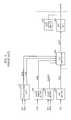
- FIG. 3is block diagram showing a conventional ODT operation unit.
- the conventional ODT operation unitincludes a delay locked loop (DLL) 310 , a clock enable buffer 320 , a clock buffer 330 , an ODT buffer 340 , an ODT controller 350 , an RTT formation unit 360 and a data output buffer 370 .
- DLLdelay locked loop
- the DLL 310receives the external clock signal CLK and an external clock bar signal CLKB to generate a rising clock signal RCLK and a falling clock signal FCLK.
- the clock enable buffer 320receives the clock enable signal CKE for buffering the clock enable signal CKE and outputs the buffered signals as a buffered clock enable signal ICKE.
- the clock buffer 330receives the external clock signal CLK and the external clock bar signal CLKB to generate an ODT control clock signal CLKODT for controlling the ODT controller 350 .
- the ODT buffer 340compares an ODT signal ODT with a reference voltage to output an ODT comparison signal ODTI.
- the ODT controller 350receives the buffered clock enable signal ICKE, the ODT control clock signal CLKODT, the ODT comparison signal ODTI, the rising clock signal RCLK and the falling clock signal FCLK to generate an RTT formation control signal ODTF.
- the RTT formation unit 360turns on/off the RTT in response to the RTT formation control signal ODTF, and the data output buffer 370 provides data on a data bus through a combination with an output signal of the RTT formation unit 360 .
- FIG. 4is a schematic circuit diagram showing the RTT formation unit 360 and the data output buffer 370 .
- a p-channel metal oxide semiconductor (PMOS) transistor MP 1 connected to a power supply voltage VDDQ and an n-channel metal oxide semiconductor (NMOS) transistor MN 1 connected to a ground voltage VSSQare turned on. Therefore, an output signal of the RTT formation unit 360 is terminated by division of resistors R 1 and R 2 . This is called ‘ODT turn on’.
- the resistor R 1 and R 2are connected in series between the PMOS transistor MP 1 and the NMOS transistor MN 1 .
- the RTT formation control signal ODTFwhich changes from a logic high level to a logic low level is inputted to the RTT formation unit 360 , the PMOS transistor MP 1 and the NMOS transistor MN 1 are turned off. Therefore, the turned-on termination becomes turned off. This is called ‘ODT turn off’.
- output signals of the RTT formation unit 360 and the data output buffer 370are commonly coupled to be connected to a data output pin (DQ pin).
- DQ pindata output pin
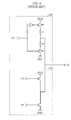
- FIG. 5is a timing diagram showing an operation of the ODT controller 350 .
- the ODT controller 350When the clock enable signal CKE is changed from a logic low level to a logic high level at the power down mode, the ODT controller 350 becomes in the active-standby mode.
- the DLL 310is disabled and is not operated. Even though the DLL 310 is enabled again when the precharge power down mode is terminated, the DLL 310 can not be operated normally at the same time when the clock enable signal CKE is changed from a logic low level to a logic high level. That is, the DLL 310 requires a predetermined set up time to be operated normally after the DLL 310 is enabled.
- the RTTmay be generated abnormally since clock signals generated by the DLL 310 are not generated when the precharge power down mode is terminated.
- ODTon die termination
- an ODT mode transfer circuitfor use in a semiconductor memory device, including: a delay locked loop (DLL) for receiving an external clock signal in order to generate a DLL clock signal according to a power down mode and an active-standby mode; an ODT mode signal generation means for generating an ODT mode signal in response to the DLL clock signal and a clock enable signal; and an ODT control means for generating a termination resistor (RTT) signal in response to an ODT signal and the ODT mode signal.
- DLLdelay locked loop
- RTTtermination resistor
- FIG. 1is a timing diagram showing an operation of an on die termination (ODT) in an active-standby mode according to the prior art
- FIG. 2is a timing diagram showing an operation of an ODT in a power down mode according to the prior art
- FIG. 3is block diagram showing a conventional ODT operation unit
- FIG. 4is a schematic circuit diagram showing an RTT formation unit and a data output buffer shown in FIG. 3 ;
- FIG. 5is a timing diagram showing an operation of an ODT controller shown in FIG. 3 ;
- FIG. 6is a block diagram showing an ODT mode transfer circuit in accordance with a preferred embodiment of the present invention.
- FIG. 7is a schematic circuit diagram depicting an ODT mode signal generator shown in FIG. 6 ;
- FIG. 8is a schematic circuit diagram showing an ODT controller shown in FIG. 6 ;
- FIG. 9is a timing diagram showing an operation of an ODT mode transfer circuit in accordance with the preferred embodiment of the present invention.
- ODTon die termination
- FIG. 6is a block diagram showing an ODT mode transfer circuit in accordance with a preferred embodiment of the present invention.
- the ODT mode transfer circuitincludes a delay locked loop (DLL) 310 , a clock enable buffer 320 , a clock buffer 330 , an ODT controller 350 , an ODT mode signal generator 650 , an ODT controller 660 , an RTT formation unit 360 and a data output buffer.
- DLLdelay locked loop
- the DLL 310receives an external clock signal CLK and an external clock bar signal CLKB in order to generate a rising clock signal RCLK and a falling clock signal FCLK.
- the clock enable buffer 320buffers a clock enable signal CKE for outputting the buffered signal as a buffed clock enable signal ICKE.
- the clock buffer 330receives the external clock signal CLK and the external clock bar signal CLKB to generate an ODT control clock signal CLKODT for controlling the ODT controller 660 .
- the ODT buffer 340compares an ODT signal ODT with a reference voltage in order to output an ODT comparison signal ODTI.
- the ODT mode signal generator 650receives the rising clock signal RCLK, the falling clock signal FCLK and the buffered clock enable signal ICKE for generating an ODT mode signal CKEODT.
- the ODT mode signal generator 650converts an ODT mode from a power down mode to an active-standby mode when the rising clock signal RCLK and the falling clock signal FCLK are stably generated by the DLL 310 after a power down mode exit.
- the ODT controller 660receives the rising clock signal RCLK, the falling clock signal FCLK, the ODT control clock signal CLKODT, the buffered clock enable signal ICKE, the ODT comparison signal ODTI and the ODT mode signal CKEODT in order to generate an RTT formation control signal ODTF for controlling the RTT formation unit 360 .
- the RTT formation unit 360turns on/off a termination resistor (RTT) in response to the RTT formation control signal ODTF, and the data output buffer 370 provides data n a data bus through a combination with an output signal of the RTT formation unit 360 .
- RTTtermination resistor
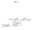
- FIG. 7is a schematic circuit diagram depicting the ODT mode signal generator 650 shown in FIG. 6 .
- the ODT mode signal generator 650includes a NOR gate 701 , a first NAND gate 703 , a second NAND gate 705 and a first inverter 707 .
- the NOR gate 701performs a logic NOR operation to the rising clock signal RCLK and the falling clock signal FCLK and outputs the result of the logic NOR operation to the first NAND gate 703 .
- the first and the second NAND gate 703 and 705forms a latch unit for latching and outputting the buffered clock enable signal ICKE.
- the first inverter 707inverts an output signal of the second NAND gate 705 in order to output the inverted signal as the ODT mode signal CKEODT.
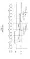
- FIG. 8is a schematic circuit diagram showing the ODT controller 660 shown in FIG. 6 .
- the ODT controller 660includes an internal control signal generation unit 801 and an RTT formation control signal generation unit 802 .
- the ODT controller 660receives the ODT control clock signal CLKODT, the ODT mode signal CKEODT and the rising and the falling clock signals RCLK and FCLK for generating a plurality of internal control signals.
- the plurality of internal control signalsincludes a first internal control signal CLKD 1 and its inverted signal, i.e., a first internal control bar signal CLKDB 1 ; a second internal control signal CLKD 2 and its inverted signal, i.e., a second internal control bar signal CLKDB 2 ; a third internal control signal RCLKD and its inverted signal, i.e., a third internal control bar signal RCLKDB; and, a fourth internal control signal FCLKD and its inverted signal, i.e., a fourth internal control bar signal FCLKDB.
- the RTT formation control signal generation unit 802receives the plurality of internal control signals in order to generate the RTT formation control signal ODTF in response to the ODT comparison signal ODTI.
- the internal control signal generation unit 801includes a first to a fourth unit internal control signal generator 810 to 840 .
- the first unit internal control signal generator 810includes a third NAND gate 811 , a first transfer gate 812 , a second to a fourth inverters 813 to 815 .
- the third NAND gate 811performs a logic NAND operation to the ODT control clock signal CLKODT and the ODT mode signal CKEODT and outputs the result of the logic NAND operation to the first transfer gate 812 and the third inverter 814 .
- the first transfer gate 812transfers an output signal of the third NAND gate 811 to the second inverter 813
- the second inverter 813buffers an output signal of the first transfer gate 812 in order to output the buffered signal as the first internal control signal CLKD 1 .
- the third and the fourth inverters 814 and 815buffer the output signal of the third NAND gate 811 in order to output the buffered signal as the first internal control bar signal CLKDB 1 .
- the second unit internal control signal generator 820includes a fifth inverter 821 , a fourth NAND gate 822 , a second transfer gate 823 , a sixth to an eighth inverters 824 to 826 .
- the fifth inverter 821buffers the ODT control clock signal CLKODT for outputting the buffered signal to the fourth NAND gate 822 .
- the fourth NAND gate 822performs a logic NAND operation to an output signal of the fifth inverter 821 and the ODT mode signal CKEODT in order to output the result of the logic NAND operation to the second transfer gate 823 and the seventh inverter 825 .
- the second transfer gate 823transfers an output signal of the fourth NAND gate 822 to the sixth inverter 824
- the sixth inverter 824buffers an output signal of the second transfer gate 823 in order to output the buffered signal as the second internal control bar signal CLKDB 2 .
- the seventh and the eighth inverters 825 and 826buffer the output signal of the fourth NAND gate 822 in order to output the buffered signal as the second internal control signal CLKD 2 .
- the third unit internal control signal generator 830includes a ninth inverter 831 , a fifth NAND gate 832 , a third transfer gate 833 , a tenth to a twelfth inverters 834 to 836 .
- the ninth inverter 831buffers the rising clock signal RCLK for outputting the buffered signal to the fifth NAND gate 832 .
- the fifth NAND gate 832performs a logic NAND operation to an output signal of the ninth inverter 831 and the ODT mode signal CKEODT in order to output the result of the logic NAND operation to the third transfer gate 833 and the eleventh inverter 835 .
- the third transfer gate 833transfers an output signal of the fifth NAND gate 832 to the tenth inverter 834 , and the tenth inverter 834 buffers an output signal of the third transfer gate 833 in order to output the buffered signal as the third internal control bar signal RCLKDB.
- the eleventh and the twelfth inverters 835 and 836buffer the output signal of the fifth NAND gate 832 in order to output the buffered signal as the third internal control signal RCLKD.
- the fourth unit internal control signal generator 840includes a thirteenth inverter 841 , a sixth NAND gate 842 , a fourth transfer gate 843 , a fourteenth to a sixteenth inverters 844 to 846 .
- the thirteenth inverter 841buffers the falling clock signal FCLK for outputting the buffered signal to the sixth NAND gate 842 .
- the sixth NAND gate 842performs a logic NAND operation to an output signal of the thirteenth inverter 841 and the ODT mode signal CKEODT in order to output the result of the logic NAND operation to the fourth transfer gate 843 and the fifteenth inverter 845 .
- the fourth transfer gate 843transfers an output signal of the thirteenth NAND gate 842 to the fourteenth inverter 844
- the fourteenth inverter 844buffers an output signal of the fourth transfer gate 843 in order to output the buffered signal as the fourth internal control bar signal FCLKDB.
- the fifteenth and the sixteenth inverters 845 and 846buffer the output signal of the sixth NAND gate 842 in order to output the buffered signal as the fourth internal control signal FCLKD.
- the RTT formation control signal generation unit 802includes a signal output unit 857 and a first to a sixth latch units 851 to 856 .
- the first latch unit 851includes a fifth transfer gate 8511 , a seventeenth and an eighteenth inverters 8512 and 8513 .
- the fifth transfer gate 8511transfers the ODT comparison signal ODTI to the seventeenth and the eighteenth inverters 8512 and 8513 when the first internal control signal CLKD 1 is in a logic low level.
- the seventeenth and the eighteenth inverters 8512 and 8513serve to latch an output signal of the fifth transfer gate 8511 in order to output the output signal of the fifth transfer gate 8511 to a first node NA.
- the second latch unit 852includes a sixth transfer gate 8521 , a nineteenth and a twentieth inverters 8522 and 8523 .
- the sixth transfer gate 8521transfers an output signal of the first node NA to the nineteenth and the twentieth inverters 8522 and 8523 when the second internal control signal CLKD 2 is in a logic high level.
- the nineteenth and the twentieth inverters 8522 and 8523serve to latch an output signal of the sixth transfer gate 8521 in order to output the output signal of the sixth transfer gate 8521 to a second node NB.
- the third latch unit 853includes a seventh transfer gate 8531 , a twenty first and a twenty second inverters 8532 and 8533 .
- the seventh transfer gate 8531transfers an output signal of the second node NB to the twenty first and the twenty second inverters 8532 and 8533 when the first internal control signal CLKD 1 is in a logic low level.
- the twenty first and the twenty second inverters 8532 and 8533serve to latch an output signal of the seventh transfer gate 8531 in order to output the output signal of the seventh transfer gate 8531 to a third node NC.
- the fourth latch unit 854includes an eighth transfer gate 8541 , a twenty third and a twenty fourth inverters 8542 and 8543 .
- the eighth transfer gate 8541transfers an output signal of the third node NC to the twenty third and the twenty fourth inverters 8542 and 8543 when the fourth internal control signal FCLKD is in a logic high level.
- the twenty third and the twenty fourth inverters 8542 and 8543serve to latch an output signal of the eighth transfer gate 8541 in order to output the output signal of the eighth transfer gate 8541 to a fourth node ND.
- the fifth latch unit 855includes a ninth transfer gate 8551 , a twenty fifth and a twenty sixth inverters 8552 and 8553 .
- the ninth transfer gate 8551transfers an output signal of the fourth node ND to the twenty fifth and the twenty sixth inverters 8552 and 8553 when the third internal control signal RCLKD is in a logic high level.
- the twenty fifth and the twenty sixth inverters 8552 and 8553serve to latch an output signal of the ninth transfer gate 8551 in order to output the output signal of the ninth transfer gate 8551 to a fifth node NE.
- the sixth latch unit 856includes a tenth transfer gate 8561 , a twenty seventh and a twenty eighth inverters 8562 and 8563 .
- the tenth transfer gate 8561transfers an output signal of the fifth node NE to the twenty seventh and the twenty eighth inverters 8562 and 8563 when the fourth internal control signal FCLKD is in a logic high level.
- the twenty seventh and the twenty eighth inverters 8562 and 8563serve to latch an output signal of the tenth transfer gate 8561 in order to output the output signal of the tenth transfer gate 8561 to a sixth node NF.
- the signal output unit 857includes a twenty ninth inverter 8571 and a seventh NAND gate 8572 .
- the twenty ninth inverter 8571buffers an output signal of the sixth node NF to output the buffered signal to the seventh NAND gate 8572 .
- the seventh NAND gate 8572performs a logic NAND operation to an output signal of the twenty ninth inverter 8571 and the output signal of the fifth node NE to thereby output the result of the logic NAND operation as the RTT formation control signal ODTF.
- the first, the third and the fifth nodes NA, NC and NEare in a logic high level; and, the second, the fourth and the sixth nodes NB, ND and NF are in a logic low level.
- FIG. 9is a timing diagram showing an operation of the ODT mode transfer circuit in accordance with the preferred embodiment of the present invention.
- a section (A)shows the operation of the ODT mode transfer circuit at the active-standby mode. Referring to the section (A), the operation of the ODT mode transfer circuit is described below.
- the RTTis turned-on at T 3 after 2 clock cycles of the external clock signal CLK, i.e., after an ODT turn-on delay time tAOND.
- the ODT comparison signal ODTIis latched by the first latch unit 851 in response to a rising edge of the ODT control clock signal CLKODT at T 1 . Then, the ODT comparison signal ODTI latched by the first latch unit 851 is passed through the second latch unit 852 and becomes in a logic high level. Thereafter, the third node NC becomes in a logic low level in response to a falling edge of the ODT control clock signal CLKODT at T′, and, the fourth node ND becomes in a logic high level in response to a rising edge of the falling clock signal FCLK between T 1 ′ and T 2 . Thereafter, the fifth node NE becomes in a logic low level in response to a rising edge of the rising clock signal RCLK, and, thus, the RTT formation control signal ODTF is activated as logic high level.
- the section (B)shows the operation of the ODT mode transfer circuit at the power down mode. Referring to the section (B), the operation of the ODT mode transfer circuit is described below.
- the buffered clock enable signal ICKEis in a logic low level at the power down mode
- the first internal control signal CLKD 1is in a logic low level
- the second internal control signal CLKD 2is in a logic high level
- the third internal control signal RCLKDis in a logic high level
- the fourth internal control signal FCLKDis in a logic high level.
- the RTT formation control signal ODTFis activated based on the plurality of internal control signals. Therefore, at the power down mode, the ODT mode transfer circuit asynchronously generates the RTT formation control signal ODTF not using clock signals generated by the DLL 310 , i.e., the rising clock signal RCLK and the falling clock signal FCLK.
- the RTTis turned-off, if the ODT signal ODT becomes in a logic low level at T 3 , the RTT is turned-off after 2.5 clock cycles of the external clock signal CLK.
- the ODT mode transfer circuitsince the ODT mode transfer circuit does not use a DLL clock signal at the power down mode in order to generate the RTT formation control signal ODTF, the ODT mode transfer circuit can stably generate the RTT formation control signal ODTF when the power down mode is terminated.
Landscapes
- Dram (AREA)
- Logic Circuits (AREA)
Abstract
Description
- The present invention relates to an on die termination (ODT) technology; and, more particularly, to an ODT technology capable of properly operating an ODT circuit by shifting a mode conversion until an output clock signal of a delay locked loop (DLL) is stabilized after a power down exit, in case when a semiconductor memory device converts an operation mode from a power down mode to an active-standby mode.
- On die termination (ODT) technology is introduced to improve signal integrity by minimizing signal reflection in an interface between a system and a semiconductor memory device, which are based on stub series termination logic (SSTL) II. Due to the introduction of the ODT technology, a termination voltage (VTT) and a termination resistor (RTT) can be provided by a semiconductor memory device and a memory controller in a double data rate-II synchronous dynamic random access memory (DDR-II SDRAM), instead of a motherboard.
- The termination technology is described below in detail.
- It is assumed that there are two ranks on a memory module. When the memory controller reads out data from a DRAM of a first rank, the memory controller applies an ODT signal of a logic high level to the DRAM of a second rank. At this time, the DRAM of the second rank forms a termination on a data bus which is shared with the first rank. This is called ‘termination resistor (RTT) formation’.
FIG. 1 is a timing diagram showing an operation of the ODT in an active-standby mode according to the prior art, andFIG. 2 is a timing diagram showing an operation of the ODT in the power down mode according to the prior art.- Referring to
FIGS. 1 and 2 , whether DRAM is in the active-standby mode or the power down mode is determined depending on a starting point of the RTT formation generated in response to the ODT signal. - In the active-standby mode, the ODT circuit provides the ODT signal which changes from a logic low level to a logic high level in synchronization with a rising edge or a falling edge of a clock signal outputted from a delay locked loop (DLL). Thereafter, an external data bus is terminated by the RTT formation in synchronization with a rising edge of an external clock signal CLK after a delay time as much as two clock cycles of the external clock signal CLK. The delay time is called an ODT turn-on delay time (tAOND).
- When the ODT circuit provides the ODT signal which changes from a logic high level to a logic low level, the RTT becomes turned-off in synchronization with a falling edge of the external clock signal CLK after a delay time as much as 2.5 clock cycles. The delay time is called an ODT turn-off delay time (tAOFD).
- Meanwhile, there are two kinds of the power down mode in the DRAM.
- When a clock enable signal CKE of a logic low level is applied, and, thus, the DRAM enters the power down mode, if a certain signal for performing a read operation or a write operation is accessed to any one of banks in the DRAM, the DRAM enters the power down mode from an active mode. This is called an active power down mode.
- On the other hand, if there is no signal access to the any bank of the DRAM, the DRAM enters the power down mode from a precharge mode. This is called a precharge power down mode.
- In the power down mode, the DLL is turned-off, and particularly in the precharge power down mode, even clock signals inputted to a delay unit of the DLL are gated off in order to reduce power consumption of the DRAM, and the DLL is not operated and just maintains a previous locking information.
- Accordingly, in the precharge power down mode, the output signal of the DLL which is necessary for forming the RTT in the DRAM cannot be used. Therefore, there is required that the minimum value and the maximum value of a power down turn-on time tAONPD and a power down turn-off time tAOFPD have to secure larger margin than that of the ODT turn-on delay time tAOND and the ODT turn-off delay time tAOFD.
FIG. 3 is block diagram showing a conventional ODT operation unit.- As shown, the conventional ODT operation unit includes a delay locked loop (DLL)310, a clock enable
buffer 320, aclock buffer 330, anODT buffer 340, anODT controller 350, anRTT formation unit 360 and adata output buffer 370. - The
DLL 310 receives the external clock signal CLK and an external clock bar signal CLKB to generate a rising clock signal RCLK and a falling clock signal FCLK. - The clock enable
buffer 320 receives the clock enable signal CKE for buffering the clock enable signal CKE and outputs the buffered signals as a buffered clock enable signal ICKE. - The
clock buffer 330 receives the external clock signal CLK and the external clock bar signal CLKB to generate an ODT control clock signal CLKODT for controlling theODT controller 350. - The
ODT buffer 340 compares an ODT signal ODT with a reference voltage to output an ODT comparison signal ODTI. TheODT controller 350 receives the buffered clock enable signal ICKE, the ODT control clock signal CLKODT, the ODT comparison signal ODTI, the rising clock signal RCLK and the falling clock signal FCLK to generate an RTT formation control signal ODTF. - The
RTT formation unit 360 turns on/off the RTT in response to the RTT formation control signal ODTF, and thedata output buffer 370 provides data on a data bus through a combination with an output signal of theRTT formation unit 360. FIG. 4 is a schematic circuit diagram showing theRTT formation unit 360 and thedata output buffer 370.- If the RTT formation control signal ODTF which changes from a logic low level to a logic high level is inputted to the
RTT formation unit 360, a p-channel metal oxide semiconductor (PMOS) transistor MP1 connected to a power supply voltage VDDQ and an n-channel metal oxide semiconductor (NMOS) transistor MN1 connected to a ground voltage VSSQ are turned on. Therefore, an output signal of theRTT formation unit 360 is terminated by division of resistors R1 and R2. This is called ‘ODT turn on’. Herein, the resistor R1 and R2 are connected in series between the PMOS transistor MP1 and the NMOS transistor MN1. - On the other hand, if the RTT formation control signal ODTF which changes from a logic high level to a logic low level is inputted to the
RTT formation unit 360, the PMOS transistor MP1 and the NMOS transistor MN1 are turned off. Therefore, the turned-on termination becomes turned off. This is called ‘ODT turn off’. - Generally, output signals of the
RTT formation unit 360 and thedata output buffer 370 are commonly coupled to be connected to a data output pin (DQ pin). FIG. 5 is a timing diagram showing an operation of theODT controller 350.- When the clock enable signal CKE is changed from a logic low level to a logic high level at the power down mode, the
ODT controller 350 becomes in the active-standby mode. - Herein, at the precharge power down mode, the DLL310 is disabled and is not operated. Even though the DLL310 is enabled again when the precharge power down mode is terminated, the
DLL 310 can not be operated normally at the same time when the clock enable signal CKE is changed from a logic low level to a logic high level. That is, the DLL310 requires a predetermined set up time to be operated normally after theDLL 310 is enabled. - Therefore, the RTT may be generated abnormally since clock signals generated by the
DLL 310 are not generated when the precharge power down mode is terminated. - It is, therefore, an object of the present invention to provide an on die termination (ODT) mode transfer circuit which performs an ODT operation stably.
- In accordance with an aspect of the present invention, there is provided an ODT mode transfer circuit, for use in a semiconductor memory device, including: a delay locked loop (DLL) for receiving an external clock signal in order to generate a DLL clock signal according to a power down mode and an active-standby mode; an ODT mode signal generation means for generating an ODT mode signal in response to the DLL clock signal and a clock enable signal; and an ODT control means for generating a termination resistor (RTT) signal in response to an ODT signal and the ODT mode signal.
- The above and other objects and features of the present invention will become apparent from the following description of preferred embodiments taken in conjunction with the accompanying drawings, in which:
FIG. 1 is a timing diagram showing an operation of an on die termination (ODT) in an active-standby mode according to the prior art;FIG. 2 is a timing diagram showing an operation of an ODT in a power down mode according to the prior art;FIG. 3 is block diagram showing a conventional ODT operation unit;FIG. 4 is a schematic circuit diagram showing an RTT formation unit and a data output buffer shown inFIG. 3 ;FIG. 5 is a timing diagram showing an operation of an ODT controller shown inFIG. 3 ;FIG. 6 is a block diagram showing an ODT mode transfer circuit in accordance with a preferred embodiment of the present invention;FIG. 7 is a schematic circuit diagram depicting an ODT mode signal generator shown inFIG. 6 ;FIG. 8 is a schematic circuit diagram showing an ODT controller shown inFIG. 6 ; andFIG. 9 is a timing diagram showing an operation of an ODT mode transfer circuit in accordance with the preferred embodiment of the present invention.- Hereinafter, an on die termination (ODT) mode transfer circuit for use in a semiconductor memory device in accordance with a preferred embodiment of the present invention will be described in detail referring to the accompanying drawings.
FIG. 6 is a block diagram showing an ODT mode transfer circuit in accordance with a preferred embodiment of the present invention.- As shown, the ODT mode transfer circuit includes a delay locked loop (DLL)310, a clock enable
buffer 320, aclock buffer 330, anODT controller 350, an ODTmode signal generator 650, anODT controller 660, anRTT formation unit 360 and a data output buffer. - The
DLL 310 receives an external clock signal CLK and an external clock bar signal CLKB in order to generate a rising clock signal RCLK and a falling clock signal FCLK. - The clock enable
buffer 320 buffers a clock enable signal CKE for outputting the buffered signal as a buffed clock enable signal ICKE. - The
clock buffer 330 receives the external clock signal CLK and the external clock bar signal CLKB to generate an ODT control clock signal CLKODT for controlling theODT controller 660. - The
ODT buffer 340 compares an ODT signal ODT with a reference voltage in order to output an ODT comparison signal ODTI. - The ODT
mode signal generator 650 receives the rising clock signal RCLK, the falling clock signal FCLK and the buffered clock enable signal ICKE for generating an ODT mode signal CKEODT. The ODTmode signal generator 650 converts an ODT mode from a power down mode to an active-standby mode when the rising clock signal RCLK and the falling clock signal FCLK are stably generated by theDLL 310 after a power down mode exit. - The
ODT controller 660 receives the rising clock signal RCLK, the falling clock signal FCLK, the ODT control clock signal CLKODT, the buffered clock enable signal ICKE, the ODT comparison signal ODTI and the ODT mode signal CKEODT in order to generate an RTT formation control signal ODTF for controlling theRTT formation unit 360. - The
RTT formation unit 360 turns on/off a termination resistor (RTT) in response to the RTT formation control signal ODTF, and thedata output buffer 370 provides data n a data bus through a combination with an output signal of theRTT formation unit 360. FIG. 7 is a schematic circuit diagram depicting the ODTmode signal generator 650 shown inFIG. 6 .- As shown, the ODT
mode signal generator 650 includes a NORgate 701, afirst NAND gate 703, asecond NAND gate 705 and afirst inverter 707. - The NOR
gate 701 performs a logic NOR operation to the rising clock signal RCLK and the falling clock signal FCLK and outputs the result of the logic NOR operation to thefirst NAND gate 703. - The first and the
second NAND gate - The
first inverter 707 inverts an output signal of thesecond NAND gate 705 in order to output the inverted signal as the ODT mode signal CKEODT. FIG. 8 is a schematic circuit diagram showing theODT controller 660 shown inFIG. 6 .- As shown, the
ODT controller 660 includes an internal controlsignal generation unit 801 and an RTT formation controlsignal generation unit 802. - The
ODT controller 660 receives the ODT control clock signal CLKODT, the ODT mode signal CKEODT and the rising and the falling clock signals RCLK and FCLK for generating a plurality of internal control signals. Herein, the plurality of internal control signals includes a first internal control signal CLKD1 and its inverted signal, i.e., a first internal control bar signal CLKDB1; a second internal control signal CLKD2 and its inverted signal, i.e., a second internal control bar signal CLKDB2; a third internal control signal RCLKD and its inverted signal, i.e., a third internal control bar signal RCLKDB; and, a fourth internal control signal FCLKD and its inverted signal, i.e., a fourth internal control bar signal FCLKDB. - The RTT formation control
signal generation unit 802 receives the plurality of internal control signals in order to generate the RTT formation control signal ODTF in response to the ODT comparison signal ODTI. - In detail, the internal control
signal generation unit 801 includes a first to a fourth unit internalcontrol signal generator 810 to840. - The first unit internal
control signal generator 810 includes athird NAND gate 811, afirst transfer gate 812, a second to afourth inverters 813 to815. - The
third NAND gate 811 performs a logic NAND operation to the ODT control clock signal CLKODT and the ODT mode signal CKEODT and outputs the result of the logic NAND operation to thefirst transfer gate 812 and the third inverter814. Thefirst transfer gate 812 transfers an output signal of thethird NAND gate 811 to thesecond inverter 813, and thesecond inverter 813 buffers an output signal of thefirst transfer gate 812 in order to output the buffered signal as the first internal control signal CLKD1. The third and the fourth inverters814 and815 buffer the output signal of thethird NAND gate 811 in order to output the buffered signal as the first internal control bar signal CLKDB1. - Similarly, the second unit internal
control signal generator 820 includes afifth inverter 821, afourth NAND gate 822, asecond transfer gate 823, a sixth to aneighth inverters 824 to826. - The
fifth inverter 821 buffers the ODT control clock signal CLKODT for outputting the buffered signal to thefourth NAND gate 822. Thefourth NAND gate 822 performs a logic NAND operation to an output signal of thefifth inverter 821 and the ODT mode signal CKEODT in order to output the result of the logic NAND operation to thesecond transfer gate 823 and the seventh inverter825. Thesecond transfer gate 823 transfers an output signal of thefourth NAND gate 822 to thesixth inverter 824, and thesixth inverter 824 buffers an output signal of thesecond transfer gate 823 in order to output the buffered signal as the second internal control bar signal CLKDB2. The seventh and the eighth inverters825 and826 buffer the output signal of thefourth NAND gate 822 in order to output the buffered signal as the second internal control signal CLKD2. - Likewise, the third unit internal
control signal generator 830 includes aninth inverter 831, afifth NAND gate 832, athird transfer gate 833, a tenth to atwelfth inverters 834 to836. - The
ninth inverter 831 buffers the rising clock signal RCLK for outputting the buffered signal to thefifth NAND gate 832. Thefifth NAND gate 832 performs a logic NAND operation to an output signal of theninth inverter 831 and the ODT mode signal CKEODT in order to output the result of the logic NAND operation to thethird transfer gate 833 and the eleventh inverter835. Thethird transfer gate 833 transfers an output signal of thefifth NAND gate 832 to thetenth inverter 834, and thetenth inverter 834 buffers an output signal of thethird transfer gate 833 in order to output the buffered signal as the third internal control bar signal RCLKDB. The eleventh and the twelfth inverters835 and836 buffer the output signal of thefifth NAND gate 832 in order to output the buffered signal as the third internal control signal RCLKD. - The fourth unit internal
control signal generator 840 includes athirteenth inverter 841, asixth NAND gate 842, afourth transfer gate 843, a fourteenth to asixteenth inverters 844 to846. - The
thirteenth inverter 841 buffers the falling clock signal FCLK for outputting the buffered signal to thesixth NAND gate 842. Thesixth NAND gate 842 performs a logic NAND operation to an output signal of thethirteenth inverter 841 and the ODT mode signal CKEODT in order to output the result of the logic NAND operation to thefourth transfer gate 843 and the fifteenth inverter845. Thefourth transfer gate 843 transfers an output signal of thethirteenth NAND gate 842 to thefourteenth inverter 844, and thefourteenth inverter 844 buffers an output signal of thefourth transfer gate 843 in order to output the buffered signal as the fourth internal control bar signal FCLKDB. The fifteenth and the sixteenth inverters845 and846 buffer the output signal of thesixth NAND gate 842 in order to output the buffered signal as the fourth internal control signal FCLKD. - The RTT formation control
signal generation unit 802 includes asignal output unit 857 and a first to asixth latch units 851 to856. - The
first latch unit 851 includes a fifth transfer gate8511, a seventeenth and aneighteenth inverters 8512 and8513. The fifth transfer gate8511 transfers the ODT comparison signal ODTI to the seventeenth and theeighteenth inverters 8512 and8513 when the first internal control signal CLKD1 is in a logic low level. The seventeenth and theeighteenth inverters 8512 and8513 serve to latch an output signal of the fifth transfer gate8511 in order to output the output signal of the fifth transfer gate8511 to a first node NA. - The
second latch unit 852 includes asixth transfer gate 8521, a nineteenth and atwentieth inverters 8522 and8523. Thesixth transfer gate 8521 transfers an output signal of the first node NA to the nineteenth and thetwentieth inverters 8522 and8523 when the second internal control signal CLKD2 is in a logic high level. The nineteenth and thetwentieth inverters 8522 and8523 serve to latch an output signal of thesixth transfer gate 8521 in order to output the output signal of thesixth transfer gate 8521 to a second node NB. - The
third latch unit 853 includes a seventh transfer gate8531, a twenty first and a twentysecond inverters 8532 and8533. The seventh transfer gate8531 transfers an output signal of the second node NB to the twenty first and the twentysecond inverters 8532 and8533 when the first internal control signal CLKD1 is in a logic low level. The twenty first and the twentysecond inverters 8532 and8533 serve to latch an output signal of the seventh transfer gate8531 in order to output the output signal of the seventh transfer gate8531 to a third node NC. - The
fourth latch unit 854 includes aneighth transfer gate 8541, a twenty third and a twentyfourth inverters 8542 and8543. Theeighth transfer gate 8541 transfers an output signal of the third node NC to the twenty third and the twentyfourth inverters 8542 and8543 when the fourth internal control signal FCLKD is in a logic high level. The twenty third and the twentyfourth inverters 8542 and8543 serve to latch an output signal of theeighth transfer gate 8541 in order to output the output signal of theeighth transfer gate 8541 to a fourth node ND. - The
fifth latch unit 855 includes a ninth transfer gate8551, a twenty fifth and a twentysixth inverters sixth inverters sixth inverters - The
sixth latch unit 856 includes a tenth transfer gate8561, a twenty seventh and a twentyeighth inverters 8562 and8563. The tenth transfer gate8561 transfers an output signal of the fifth node NE to the twenty seventh and the twentyeighth inverters 8562 and8563 when the fourth internal control signal FCLKD is in a logic high level. The twenty seventh and the twentyeighth inverters 8562 and8563 serve to latch an output signal of the tenth transfer gate8561 in order to output the output signal of the tenth transfer gate8561 to a sixth node NF. - The
signal output unit 857 includes a twentyninth inverter 8571 and aseventh NAND gate 8572. - The twenty
ninth inverter 8571 buffers an output signal of the sixth node NF to output the buffered signal to theseventh NAND gate 8572. Theseventh NAND gate 8572 performs a logic NAND operation to an output signal of the twentyninth inverter 8571 and the output signal of the fifth node NE to thereby output the result of the logic NAND operation as the RTT formation control signal ODTF. - Meanwhile, at an initial state, the first, the third and the fifth nodes NA, NC and NE are in a logic high level; and, the second, the fourth and the sixth nodes NB, ND and NF are in a logic low level.
FIG. 9 is a timing diagram showing an operation of the ODT mode transfer circuit in accordance with the preferred embodiment of the present invention.- A section (A) shows the operation of the ODT mode transfer circuit at the active-standby mode. Referring to the section (A), the operation of the ODT mode transfer circuit is described below.
- If the ODT signal ODT is activated as a logic high level at T1′, the RTT is turned-on at T3 after 2 clock cycles of the external clock signal CLK, i.e., after an ODT turn-on delay time tAOND.
- In detail, the ODT comparison signal ODTI is latched by the
first latch unit 851 in response to a rising edge of the ODT control clock signal CLKODT at T1. Then, the ODT comparison signal ODTI latched by thefirst latch unit 851 is passed through thesecond latch unit 852 and becomes in a logic high level. Thereafter, the third node NC becomes in a logic low level in response to a falling edge of the ODT control clock signal CLKODT at T′, and, the fourth node ND becomes in a logic high level in response to a rising edge of the falling clock signal FCLK between T1′ and T2. Thereafter, the fifth node NE becomes in a logic low level in response to a rising edge of the rising clock signal RCLK, and, thus, the RTT formation control signal ODTF is activated as logic high level. - The section (B) shows the operation of the ODT mode transfer circuit at the power down mode. Referring to the section (B), the operation of the ODT mode transfer circuit is described below.
- Since the buffered clock enable signal ICKE is in a logic low level at the power down mode, the first internal control signal CLKD1 is in a logic low level, the second internal control signal CLKD2 is in a logic high level, the third internal control signal RCLKD is in a logic high level and the fourth internal control signal FCLKD is in a logic high level. Then, the RTT formation control signal ODTF is activated based on the plurality of internal control signals. Therefore, at the power down mode, the ODT mode transfer circuit asynchronously generates the RTT formation control signal ODTF not using clock signals generated by the
DLL 310, i.e., the rising clock signal RCLK and the falling clock signal FCLK. - Meanwhile, in case that the RTT is turned-off, if the ODT signal ODT becomes in a logic low level at T3, the RTT is turned-off after 2.5 clock cycles of the external clock signal CLK.
- As described above, since the ODT mode transfer circuit does not use a DLL clock signal at the power down mode in order to generate the RTT formation control signal ODTF, the ODT mode transfer circuit can stably generate the RTT formation control signal ODTF when the power down mode is terminated.
- The present application contains subject matter related to Korean patent application No. 2004-9501, filed in the Korean Patent Office on Feb. 13, 2004, the entire contents of which being incorporated herein by reference.
- While the present invention has been described with respect to the particular embodiments, it will be apparent to those skilled in the art that various changes and modifications may be made without departing from the spirit and scope of the invention as defined in the following claims.
Claims (18)
Applications Claiming Priority (2)
| Application Number | Priority Date | Filing Date | Title |
|---|---|---|---|
| KR10-2004-0009501AKR100528164B1 (en) | 2004-02-13 | 2004-02-13 | On die termination mode transfer circuit in semiconductor memory device and its method |
| KR2004-09501 | 2004-02-13 |
Publications (2)
| Publication Number | Publication Date |
|---|---|
| US20050180229A1true US20050180229A1 (en) | 2005-08-18 |
| US7196966B2 US7196966B2 (en) | 2007-03-27 |
Family
ID=34836728
Family Applications (1)
| Application Number | Title | Priority Date | Filing Date |
|---|---|---|---|
| US10/879,650Expired - LifetimeUS7196966B2 (en) | 2004-02-13 | 2004-06-28 | On die termination mode transfer circuit in semiconductor memory device and its method |
Country Status (5)
| Country | Link |
|---|---|
| US (1) | US7196966B2 (en) |
| JP (1) | JP4693089B2 (en) |
| KR (1) | KR100528164B1 (en) |
| CN (1) | CN100476999C (en) |
| TW (1) | TWI253084B (en) |
Cited By (19)
| Publication number | Priority date | Publication date | Assignee | Title |
|---|---|---|---|---|
| US20060253738A1 (en)* | 2004-06-21 | 2006-11-09 | Stave Eric J | Real time testing using on die termination (ODT) circuit |
| US20070030030A1 (en)* | 2005-08-03 | 2007-02-08 | Micron Technology, Inc. | Method and apparatus for selecting an operating mode based on a determination of the availability of internal clock signals |
| US20070103188A1 (en)* | 2005-10-21 | 2007-05-10 | Elpida Memory, Inc. | Semiconductor memory chip with on-die termination function |
| US20070126469A1 (en)* | 2005-09-29 | 2007-06-07 | Hynix Semiconductor Inc. | Device for controlling on die termination |
| US20070126467A1 (en)* | 2005-09-29 | 2007-06-07 | Hynix Semiconductor Inc. | Test device for on die termination |
| US20070126470A1 (en)* | 2005-09-29 | 2007-06-07 | Hynix Semiconductor Inc. | Apparatus and method for controlling on die termination |
| US20080074139A1 (en)* | 2006-09-27 | 2008-03-27 | Hynix Semiconductor Inc. | Semiconductor memory device with on-die termination circuit |
| US20080159026A1 (en)* | 2006-12-04 | 2008-07-03 | Samsung Electronics Co., Ltd. | Memory systems, on-die termination (odt) circuits, and method of odt control |
| US20080191734A1 (en)* | 2007-02-09 | 2008-08-14 | Samsung Electronics Co., Ltd. | Semiconductor device including on-die termination control circuit having pipe line varying with frequency range |
| US20080204071A1 (en)* | 2007-02-27 | 2008-08-28 | Samsung Electronics Co., Ltd. | On-die termination circuit, method of controlling the same, and ODT synchronous buffer |
| US20080278192A1 (en)* | 2007-05-10 | 2008-11-13 | Hynix Semiconductor Inc. | Data output driving circuit for a semiconductor apparatus |
| US20090016124A1 (en)* | 2007-07-12 | 2009-01-15 | Hynix Semiconductor Inc. | Semiconductor memory device having on-die-termination device and operation method thereof |
| US20090102510A1 (en)* | 2007-10-23 | 2009-04-23 | Jung Hoon Park | Control circuit for controlling on-die termination impedance |
| US20090249097A1 (en)* | 2008-03-31 | 2009-10-01 | Lam Son H | Optimizing performance and power consumption during memory power down state |
| US20100036634A1 (en)* | 2008-08-08 | 2010-02-11 | Sang Jin Byeon | Apparatus and method for generating resistance calibration code in semiconductor integrated circuit |
| US7663940B2 (en) | 2007-01-08 | 2010-02-16 | Hynix Semiconductor Inc. | Semiconductor memory device and driving method thereof |
| US20110058442A1 (en)* | 2009-09-10 | 2011-03-10 | Elpida Memory, Inc. | Semiconductor device having ODT function and data processing system including the same |
| TWI391942B (en)* | 2007-11-02 | 2013-04-01 | Hynix Semiconductor Inc | On die termination device and semiconductor memory device including the same |
| TWI650766B (en)* | 2014-12-23 | 2019-02-11 | 韓商愛思開海力士有限公司 | Semiconductor devices and semiconductor systems including the same |
Families Citing this family (34)
| Publication number | Priority date | Publication date | Assignee | Title |
|---|---|---|---|---|
| KR100625298B1 (en)* | 2005-09-29 | 2006-09-15 | 주식회사 하이닉스반도체 | On Die Termination Control |
| KR100805696B1 (en) | 2005-09-29 | 2008-02-21 | 주식회사 하이닉스반도체 | Semiconductor memory device |
| KR100761359B1 (en)* | 2005-09-29 | 2007-09-27 | 주식회사 하이닉스반도체 | On-die termination control circuit and method |
| KR100849065B1 (en)* | 2005-12-15 | 2008-07-30 | 주식회사 하이닉스반도체 | Method for calibrating a driver and an ODT of a synchronous memory device |
| TWI323467B (en) | 2005-12-27 | 2010-04-11 | Hynix Semiconductor Inc | On-die termination circuit for semiconductor memory apparatus |
| KR100681879B1 (en) | 2006-01-16 | 2007-02-15 | 주식회사 하이닉스반도체 | On-die termination control |
| KR100771868B1 (en)* | 2006-02-28 | 2007-11-01 | 삼성전자주식회사 | Dynamic output buffer circuit |
| KR100780949B1 (en) | 2006-03-21 | 2007-12-03 | 삼성전자주식회사 | Semiconductor memory device capable of testing the on / off state of the ODT circuit in the data read mode |
| KR100681881B1 (en) | 2006-04-06 | 2007-02-15 | 주식회사 하이닉스반도체 | On die termination device and method of semiconductor memory |
| KR100718049B1 (en)* | 2006-06-08 | 2007-05-14 | 주식회사 하이닉스반도체 | On-die termination device of semiconductor memory and its control method |
| KR100851989B1 (en) | 2006-10-12 | 2008-08-13 | 주식회사 하이닉스반도체 | Circuit and Method for Outputting Temperature Data of Semiconductor Memory Apparatus |
| KR100780962B1 (en)* | 2006-10-27 | 2007-12-03 | 삼성전자주식회사 | Dynamic ODT mode test method and ODT mode test circuit using the method |
| KR100880835B1 (en) | 2007-01-03 | 2009-02-02 | 주식회사 하이닉스반도체 | The negative voltage supply of the memory device. |
| KR100807118B1 (en)* | 2007-01-03 | 2008-02-26 | 주식회사 하이닉스반도체 | Semiconductor memory device |
| KR100821585B1 (en) | 2007-03-12 | 2008-04-15 | 주식회사 하이닉스반도체 | On die termination circuit of semiconductor memory device |
| KR100857438B1 (en) | 2007-03-13 | 2008-09-10 | 주식회사 하이닉스반도체 | Voltage generation circuit and reference voltage generation circuit of semiconductor memory device using same |
| KR100897255B1 (en) | 2007-04-12 | 2009-05-14 | 주식회사 하이닉스반도체 | On die termination circuit and method of semiconductor memory device |
| KR100863536B1 (en)* | 2007-11-02 | 2008-10-15 | 주식회사 하이닉스반도체 | On die termination control circuit and its control method |
| KR100960012B1 (en) | 2007-12-12 | 2010-05-28 | 주식회사 하이닉스반도체 | On die termination control circuit and control method |
| KR100927401B1 (en)* | 2007-12-12 | 2009-11-19 | 주식회사 하이닉스반도체 | On die termination control circuit and control method |
| KR100933676B1 (en)* | 2008-04-30 | 2009-12-23 | 주식회사 하이닉스반도체 | Calibration circuit, semiconductor memory device including the same, and operating method of the calibration circuit |
| US7869300B2 (en)* | 2009-04-29 | 2011-01-11 | Agere Systems Inc. | Memory device control for self-refresh mode |
| US8139433B2 (en)* | 2009-05-13 | 2012-03-20 | Lsi Corporation | Memory device control for self-refresh mode |
| KR101069678B1 (en) | 2009-06-16 | 2011-10-05 | 주식회사 하이닉스반도체 | Temperature Detection Circuit of a Semiconductor Memory Apparatus |
| US9213063B2 (en) | 2014-03-26 | 2015-12-15 | Freescale Semiconductor, Inc. | Reset generation circuit for scan mode exit |
| US11217286B2 (en)* | 2016-06-27 | 2022-01-04 | SK Hynix Inc. | Semiconductor memory device with power down operation |
| US10147471B2 (en) | 2016-08-02 | 2018-12-04 | SK Hynix Inc. | Semiconductor devices and semiconductor systems |
| US10181346B2 (en) | 2016-08-02 | 2019-01-15 | SK Hynix Inc. | Semiconductor devices and operations thereof |
| KR102592359B1 (en)* | 2016-06-27 | 2023-10-20 | 에스케이하이닉스 주식회사 | Semiconductor device |
| US11133042B2 (en)* | 2016-06-27 | 2021-09-28 | SK Hynix Inc. | Semiconductor memory system and semiconductor memory device, which can be remotely initialized |
| US12424253B2 (en)* | 2016-08-02 | 2025-09-23 | SK Hynix Inc. | Semiconductor device with power-down signal generation |
| US10566038B2 (en)* | 2017-05-29 | 2020-02-18 | Samsung Electronics Co., Ltd. | Method of controlling on-die termination and system performing the same |
| US10153014B1 (en) | 2017-08-17 | 2018-12-11 | Micron Technology, Inc. | DQS-offset and read-RTT-disable edge control |
| CN112986797A (en)* | 2021-02-08 | 2021-06-18 | 昂宝电子(上海)有限公司 | Chip test circuit and method |
Citations (8)
| Publication number | Priority date | Publication date | Assignee | Title |
|---|---|---|---|---|
| US5134587A (en)* | 1990-08-17 | 1992-07-28 | Sgs-Thomson Microelectronics, Inc. | Semiconductor memory with automatic test mode exit on chip enable |
| US5706232A (en)* | 1990-08-17 | 1998-01-06 | Sgs-Thomson Microelectronics, Inc. | Semiconductor memory with multiple clocking for test mode entry |
| US6650594B1 (en)* | 2002-07-12 | 2003-11-18 | Samsung Electronics Co., Ltd. | Device and method for selecting power down exit |
| US20030235107A1 (en)* | 2002-06-21 | 2003-12-25 | Seong-Jin Jang | Memory systems and methods of operating the same in which an active termination value for a memory device is determined at a low clock frequency and commands are applied to the memory device at a higher clock frequency |
| US6699734B2 (en)* | 1998-04-02 | 2004-03-02 | Micron Technology, Inc. | Method and apparatus for coupling a semiconductor die to die terminals |
| US20040080322A1 (en)* | 2002-09-30 | 2004-04-29 | Georg Braun | Method for calibrating semiconductor devices using a common calibration reference and a calibration circuit |
| US20040100837A1 (en)* | 2002-11-20 | 2004-05-27 | Samsung Electronics Co., Ltd. | On-die termination circuit and method for reducing on-chip DC current, and memory system including memory device having the same |
| US20040141391A1 (en)* | 2003-01-03 | 2004-07-22 | Dong-Jin Lee | Synchronous semiconductor memory device having on-die termination circuit and on-die termination method |
Family Cites Families (2)
| Publication number | Priority date | Publication date | Assignee | Title |
|---|---|---|---|---|
| JP3880206B2 (en)* | 1998-07-16 | 2007-02-14 | 富士通株式会社 | Integrated circuit device |
| EP1306849B1 (en)* | 2001-10-19 | 2008-02-27 | Samsung Electronics Co., Ltd. | Devices and methods for controlling active termination resistors in a memory system |
- 2004
- 2004-02-13KRKR10-2004-0009501Apatent/KR100528164B1/ennot_activeExpired - Lifetime
- 2004-06-28TWTW093118720Apatent/TWI253084B/ennot_activeIP Right Cessation
- 2004-06-28USUS10/879,650patent/US7196966B2/ennot_activeExpired - Lifetime
- 2004-06-30JPJP2004195037Apatent/JP4693089B2/ennot_activeExpired - Fee Related
- 2004-11-04CNCNB2004100889040Apatent/CN100476999C/ennot_activeExpired - Fee Related
Patent Citations (8)
| Publication number | Priority date | Publication date | Assignee | Title |
|---|---|---|---|---|
| US5134587A (en)* | 1990-08-17 | 1992-07-28 | Sgs-Thomson Microelectronics, Inc. | Semiconductor memory with automatic test mode exit on chip enable |
| US5706232A (en)* | 1990-08-17 | 1998-01-06 | Sgs-Thomson Microelectronics, Inc. | Semiconductor memory with multiple clocking for test mode entry |
| US6699734B2 (en)* | 1998-04-02 | 2004-03-02 | Micron Technology, Inc. | Method and apparatus for coupling a semiconductor die to die terminals |
| US20030235107A1 (en)* | 2002-06-21 | 2003-12-25 | Seong-Jin Jang | Memory systems and methods of operating the same in which an active termination value for a memory device is determined at a low clock frequency and commands are applied to the memory device at a higher clock frequency |
| US6650594B1 (en)* | 2002-07-12 | 2003-11-18 | Samsung Electronics Co., Ltd. | Device and method for selecting power down exit |
| US20040080322A1 (en)* | 2002-09-30 | 2004-04-29 | Georg Braun | Method for calibrating semiconductor devices using a common calibration reference and a calibration circuit |
| US20040100837A1 (en)* | 2002-11-20 | 2004-05-27 | Samsung Electronics Co., Ltd. | On-die termination circuit and method for reducing on-chip DC current, and memory system including memory device having the same |
| US20040141391A1 (en)* | 2003-01-03 | 2004-07-22 | Dong-Jin Lee | Synchronous semiconductor memory device having on-die termination circuit and on-die termination method |
Cited By (38)
| Publication number | Priority date | Publication date | Assignee | Title |
|---|---|---|---|---|
| US20060253738A1 (en)* | 2004-06-21 | 2006-11-09 | Stave Eric J | Real time testing using on die termination (ODT) circuit |
| US7664999B2 (en)* | 2004-06-21 | 2010-02-16 | Micron Technology, Inc. | Real time testing using on die termination (ODT) circuit |
| US20070030030A1 (en)* | 2005-08-03 | 2007-02-08 | Micron Technology, Inc. | Method and apparatus for selecting an operating mode based on a determination of the availability of internal clock signals |
| US7560956B2 (en) | 2005-08-03 | 2009-07-14 | Micron Technology, Inc. | Method and apparatus for selecting an operating mode based on a determination of the availability of internal clock signals |
| US20070126469A1 (en)* | 2005-09-29 | 2007-06-07 | Hynix Semiconductor Inc. | Device for controlling on die termination |
| US20070126470A1 (en)* | 2005-09-29 | 2007-06-07 | Hynix Semiconductor Inc. | Apparatus and method for controlling on die termination |
| US7317328B2 (en) | 2005-09-29 | 2008-01-08 | Hynix Semiconductor Inc. | Test device for on die termination |
| US7365564B2 (en) | 2005-09-29 | 2008-04-29 | Hynix Semiconductor Inc. | Apparatus and method for controlling on die termination |
| US20070126467A1 (en)* | 2005-09-29 | 2007-06-07 | Hynix Semiconductor Inc. | Test device for on die termination |
| US7429871B2 (en) | 2005-09-29 | 2008-09-30 | Hynix Semiconductor Inc. | Device for controlling on die termination |
| DE102006045255B4 (en)* | 2005-09-29 | 2009-12-17 | Hynix Semiconductor Inc., Icheon | Apparatus and method for controlling signal termination on a chip |
| US7688671B2 (en) | 2005-10-21 | 2010-03-30 | Elpida Memory, Inc. | Semiconductor memory chip with on-die termination function |
| US20070103188A1 (en)* | 2005-10-21 | 2007-05-10 | Elpida Memory, Inc. | Semiconductor memory chip with on-die termination function |
| US20080074139A1 (en)* | 2006-09-27 | 2008-03-27 | Hynix Semiconductor Inc. | Semiconductor memory device with on-die termination circuit |
| US7567093B2 (en) | 2006-09-27 | 2009-07-28 | Hynix Semiconductor, Inc. | Semiconductor memory device with on-die termination circuit |
| US20080159026A1 (en)* | 2006-12-04 | 2008-07-03 | Samsung Electronics Co., Ltd. | Memory systems, on-die termination (odt) circuits, and method of odt control |
| US7786752B2 (en) | 2006-12-04 | 2010-08-31 | Samsung Electronics Co., Ltd. | Memory systems, on-die termination (ODT) circuits, and method of ODT control |
| US7663940B2 (en) | 2007-01-08 | 2010-02-16 | Hynix Semiconductor Inc. | Semiconductor memory device and driving method thereof |
| US20080191734A1 (en)* | 2007-02-09 | 2008-08-14 | Samsung Electronics Co., Ltd. | Semiconductor device including on-die termination control circuit having pipe line varying with frequency range |
| US7663397B2 (en)* | 2007-02-09 | 2010-02-16 | Samsung Electronics Co., Ltd. | Semiconductor device including on-die termination control circuit having pipe line varying with frequency range |
| US7868648B2 (en)* | 2007-02-27 | 2011-01-11 | Samsung Electronics Co., Ltd. | On-die termination circuit, method of controlling the same, and ODT synchronous buffer |
| US20080204071A1 (en)* | 2007-02-27 | 2008-08-28 | Samsung Electronics Co., Ltd. | On-die termination circuit, method of controlling the same, and ODT synchronous buffer |
| US7906986B2 (en) | 2007-05-10 | 2011-03-15 | Hynix Semiconductor Inc. | Data output driving circuit for a semiconductor apparatus |
| US20080278192A1 (en)* | 2007-05-10 | 2008-11-13 | Hynix Semiconductor Inc. | Data output driving circuit for a semiconductor apparatus |
| US20090016124A1 (en)* | 2007-07-12 | 2009-01-15 | Hynix Semiconductor Inc. | Semiconductor memory device having on-die-termination device and operation method thereof |
| US7663946B2 (en) | 2007-07-12 | 2010-02-16 | Hynix Semiconductor Inc. | Semiconductor memory device having on-die-termination device and operation method thereof |
| US20100045340A1 (en)* | 2007-10-23 | 2010-02-25 | Hynix Semiconductor Inc. | Control circuit for controlling on-die termination impedance |
| US20090102510A1 (en)* | 2007-10-23 | 2009-04-23 | Jung Hoon Park | Control circuit for controlling on-die termination impedance |
| US7629811B2 (en)* | 2007-10-23 | 2009-12-08 | Hynix Semiconductor Inc. | Control circuit for controlling on-die termination impedance |
| US7919978B2 (en)* | 2007-10-23 | 2011-04-05 | Hynix Semiconductor Inc. | Control circuit for controlling on-die termination impedance |
| TWI391942B (en)* | 2007-11-02 | 2013-04-01 | Hynix Semiconductor Inc | On die termination device and semiconductor memory device including the same |
| US20090249097A1 (en)* | 2008-03-31 | 2009-10-01 | Lam Son H | Optimizing performance and power consumption during memory power down state |
| US8719606B2 (en)* | 2008-03-31 | 2014-05-06 | Intel Corporation | Optimizing performance and power consumption during memory power down state |
| US20100036634A1 (en)* | 2008-08-08 | 2010-02-11 | Sang Jin Byeon | Apparatus and method for generating resistance calibration code in semiconductor integrated circuit |
| US8169232B2 (en)* | 2008-08-08 | 2012-05-01 | Hynix Semiconductor Inc. | Apparatus and method for generating resistance calibration code in semiconductor integrated circuit |
| US20110058442A1 (en)* | 2009-09-10 | 2011-03-10 | Elpida Memory, Inc. | Semiconductor device having ODT function and data processing system including the same |
| US8363508B2 (en)* | 2009-09-10 | 2013-01-29 | Elpida Memory, Inc. | Semiconductor device having ODT function and data processing system including the same |
| TWI650766B (en)* | 2014-12-23 | 2019-02-11 | 韓商愛思開海力士有限公司 | Semiconductor devices and semiconductor systems including the same |
Also Published As
| Publication number | Publication date |
|---|---|
| US7196966B2 (en) | 2007-03-27 |
| CN100476999C (en) | 2009-04-08 |
| JP4693089B2 (en) | 2011-06-01 |
| JP2005228458A (en) | 2005-08-25 |
| TWI253084B (en) | 2006-04-11 |
| KR100528164B1 (en) | 2005-11-15 |
| TW200527444A (en) | 2005-08-16 |
| KR20050081315A (en) | 2005-08-19 |
| CN1655279A (en) | 2005-08-17 |
Similar Documents
| Publication | Publication Date | Title |
|---|---|---|
| US7196966B2 (en) | On die termination mode transfer circuit in semiconductor memory device and its method | |
| US6928007B2 (en) | ODT mode conversion circuit and method | |
| US6768690B2 (en) | Register controlled DLL for reducing current consumption | |
| KR102401526B1 (en) | Apparatus and method for determining a phase relationship between an input clock signal and a polyphase clock signal | |
| US7280430B2 (en) | Semiconductor memory device | |
| US7038972B2 (en) | Double data rate synchronous dynamic random access memory semiconductor device | |
| US7489172B2 (en) | DLL driver control circuit | |
| US6172537B1 (en) | Semiconductor device | |
| US6791888B2 (en) | Semiconductor memory device having preamble function | |
| US6538956B2 (en) | Semiconductor memory device for providing address access time and data access time at a high speed | |
| US8023339B2 (en) | Pipe latch circuit and semiconductor memory device using the same | |
| US7471578B2 (en) | Internal voltage generation control circuit and internal voltage generation circuit using the same | |
| US6075393A (en) | Clock synchronous semiconductor device system and semiconductor devices used with the same | |
| US8406080B2 (en) | Data output control circuit of a double data rate (DDR) synchronous semiconductor memory device responsive to a delay locked loop (DLL) clock and method thereof | |
| US10811063B2 (en) | Semiconductor device | |
| US6987699B2 (en) | Clock driver in semiconductor memory device | |
| US6696862B2 (en) | Semiconductor memory device input circuit | |
| US7283421B2 (en) | Semiconductor memory device | |
| US20100277992A1 (en) | Semiconductor memory device and driving method thereof | |
| US7952957B2 (en) | Circuit for generating read and signal and circuit for generating internal clock using the same |
Legal Events
| Date | Code | Title | Description |
|---|---|---|---|
| AS | Assignment | Owner name:HYNIX SEMICONDUCTOR INC., KOREA, REPUBLIC OF Free format text:ASSIGNMENT OF ASSIGNORS INTEREST;ASSIGNOR:JIN, SEUNG-EON;REEL/FRAME:015535/0896 Effective date:20040623 | |
| STCF | Information on status: patent grant | Free format text:PATENTED CASE | |
| CC | Certificate of correction | ||
| FEPP | Fee payment procedure | Free format text:PAYOR NUMBER ASSIGNED (ORIGINAL EVENT CODE: ASPN); ENTITY STATUS OF PATENT OWNER: LARGE ENTITY | |
| FEPP | Fee payment procedure | Free format text:PAYER NUMBER DE-ASSIGNED (ORIGINAL EVENT CODE: RMPN); ENTITY STATUS OF PATENT OWNER: LARGE ENTITY | |
| FEPP | Fee payment procedure | Free format text:PAYOR NUMBER ASSIGNED (ORIGINAL EVENT CODE: ASPN); ENTITY STATUS OF PATENT OWNER: LARGE ENTITY | |
| FPAY | Fee payment | Year of fee payment:4 | |
| AS | Assignment | Owner name:658868 N.B. INC., CANADA Free format text:ASSIGNMENT OF ASSIGNORS INTEREST;ASSIGNOR:HYNIX SEMICONDUCTOR INC.;REEL/FRAME:027231/0292 Effective date:20110822 | |
| AS | Assignment | Owner name:ROYAL BANK OF CANADA, CANADA Free format text:U.S. INTELLECTUAL PROPERTY SECURITY AGREEMENT (FOR NON-U.S. GRANTORS) - SHORT FORM;ASSIGNORS:658276 N.B. LTD.;658868 N.B. INC.;MOSAID TECHNOLOGIES INCORPORATED;REEL/FRAME:027512/0196 Effective date:20111223 | |
| AS | Assignment | Owner name:CONVERSANT IP N.B. 868 INC., CANADA Free format text:CHANGE OF NAME;ASSIGNOR:658868 N.B. INC.;REEL/FRAME:032439/0547 Effective date:20140101 | |
| AS | Assignment | Owner name:CONVERSANT INTELLECTUAL PROPERTY MANAGEMENT INC., Free format text:RELEASE OF SECURITY INTEREST;ASSIGNOR:ROYAL BANK OF CANADA;REEL/FRAME:033484/0344 Effective date:20140611 Owner name:CONVERSANT IP N.B. 868 INC., CANADA Free format text:RELEASE OF SECURITY INTEREST;ASSIGNOR:ROYAL BANK OF CANADA;REEL/FRAME:033484/0344 Effective date:20140611 Owner name:CONVERSANT IP N.B. 276 INC., CANADA Free format text:RELEASE OF SECURITY INTEREST;ASSIGNOR:ROYAL BANK OF CANADA;REEL/FRAME:033484/0344 Effective date:20140611 | |
| FPAY | Fee payment | Year of fee payment:8 | |
| AS | Assignment | Owner name:ROYAL BANK OF CANADA, AS LENDER, CANADA Free format text:U.S. PATENT SECURITY AGREEMENT (FOR NON-U.S. GRANTORS);ASSIGNOR:CONVERSANT IP N.B. 868 INC.;REEL/FRAME:033707/0001 Effective date:20140611 Owner name:CPPIB CREDIT INVESTMENTS INC., AS LENDER, CANADA Free format text:U.S. PATENT SECURITY AGREEMENT (FOR NON-U.S. GRANTORS);ASSIGNOR:CONVERSANT IP N.B. 868 INC.;REEL/FRAME:033707/0001 Effective date:20140611 | |
| AS | Assignment | Owner name:CONVERSANT INTELLECTUAL PROPERTY MANAGEMENT INC., Free format text:ASSIGNMENT OF ASSIGNORS INTEREST;ASSIGNOR:CONVERSANT IP N.B. 868 INC.;REEL/FRAME:036159/0386 Effective date:20150514 | |
| AS | Assignment | Owner name:CPPIB CREDIT INVESTMENTS, INC., CANADA Free format text:AMENDED AND RESTATED U.S. PATENT SECURITY AGREEMENT (FOR NON-U.S. GRANTORS);ASSIGNOR:CONVERSANT INTELLECTUAL PROPERTY MANAGEMENT INC.;REEL/FRAME:046900/0136 Effective date:20180731 | |
| MAFP | Maintenance fee payment | Free format text:PAYMENT OF MAINTENANCE FEE, 12TH YEAR, LARGE ENTITY (ORIGINAL EVENT CODE: M1553); ENTITY STATUS OF PATENT OWNER: LARGE ENTITY Year of fee payment:12 | |
| AS | Assignment | Owner name:CONVERSANT INTELLECTUAL PROPERTY MANAGEMENT INC., CANADA Free format text:RELEASE OF U.S. PATENT AGREEMENT (FOR NON-U.S. GRANTORS);ASSIGNOR:ROYAL BANK OF CANADA, AS LENDER;REEL/FRAME:047645/0424 Effective date:20180731 Owner name:CONVERSANT INTELLECTUAL PROPERTY MANAGEMENT INC., Free format text:RELEASE OF U.S. PATENT AGREEMENT (FOR NON-U.S. GRANTORS);ASSIGNOR:ROYAL BANK OF CANADA, AS LENDER;REEL/FRAME:047645/0424 Effective date:20180731 | |
| AS | Assignment | Owner name:CONVERSANT INTELLECTUAL PROPERTY MANAGEMENT INC., CANADA Free format text:RELEASE BY SECURED PARTY;ASSIGNOR:CPPIB CREDIT INVESTMENTS INC.;REEL/FRAME:054371/0684 Effective date:20201028 | |
| AS | Assignment | Owner name:MOSAID TECHNOLOGIES INCORPORATED, CANADA Free format text:CHANGE OF NAME;ASSIGNOR:CONVERSANT INTELLECTUAL PROPERTY INC.;REEL/FRAME:058297/0853 Effective date:20210401 | |
| AS | Assignment | Owner name:MOSAID TECHNOLOGIES INCORPORATED, CANADA Free format text:CORRECTIVE ASSIGNMENT TO CORRECT THE CONVEYING PARTY'S NAME PREVIOUSLY RECORDED ON REEL 058297 FRAME 0853. ASSIGNOR(S) HEREBY CONFIRMS THE CHANGE OF NAME;ASSIGNOR:CONVERSANT INTELLECTUAL PROPERTY MANAGEMENT INC.;REEL/FRAME:064742/0953 Effective date:20210401 |