US20050179093A1 - Buried guard ring and radiation hardened isolation structures and fabrication methods - Google Patents
Buried guard ring and radiation hardened isolation structures and fabrication methodsDownload PDFInfo
- Publication number
- US20050179093A1 US20050179093A1US10/951,283US95128304AUS2005179093A1US 20050179093 A1US20050179093 A1US 20050179093A1US 95128304 AUS95128304 AUS 95128304AUS 2005179093 A1US2005179093 A1US 2005179093A1
- Authority
- US
- United States
- Prior art keywords
- region
- substrate
- well
- layer
- semiconductor device
- Prior art date
- Legal status (The legal status is an assumption and is not a legal conclusion. Google has not performed a legal analysis and makes no representation as to the accuracy of the status listed.)
- Granted
Links
- 238000000034methodMethods0.000titleclaimsabstractdescription78
- 238000002955isolationMethods0.000titleabstractdescription30
- 230000005855radiationEffects0.000titleabstractdescription25
- 238000004519manufacturing processMethods0.000titleabstractdescription17
- 239000004065semiconductorSubstances0.000claimsabstractdescription51
- 239000000758substrateSubstances0.000claimsdescription105
- 239000012535impuritySubstances0.000claimsdescription61
- 239000004020conductorSubstances0.000claimsdescription37
- 239000000463materialSubstances0.000claimsdescription20
- 150000002500ionsChemical class0.000claimsdescription13
- 230000005669field effectEffects0.000claimsdescription9
- 239000012212insulatorSubstances0.000claimsdescription8
- 238000000151depositionMethods0.000claimsdescription6
- 238000005468ion implantationMethods0.000claimsdescription6
- 229910052796boronInorganic materials0.000claimsdescription4
- 229910052698phosphorusInorganic materials0.000claimsdescription3
- 239000011574phosphorusSubstances0.000claimsdescription3
- 229910052760oxygenInorganic materials0.000claimsdescription2
- 239000001301oxygenSubstances0.000claimsdescription2
- -1boron ionsChemical class0.000claims5
- 229910001449indium ionInorganic materials0.000claims2
- 239000011810insulating materialSubstances0.000claims2
- 230000008878couplingEffects0.000claims1
- 238000010168coupling processMethods0.000claims1
- 238000005859coupling reactionMethods0.000claims1
- 238000005530etchingMethods0.000claims1
- 230000008569processEffects0.000abstractdescription23
- 230000003071parasitic effectEffects0.000abstractdescription17
- 238000013461designMethods0.000abstractdescription6
- 230000001627detrimental effectEffects0.000abstractdescription2
- XUIMIQQOPSSXEZ-UHFFFAOYSA-NSiliconChemical compound[Si]XUIMIQQOPSSXEZ-UHFFFAOYSA-N0.000description28
- 239000010703siliconSubstances0.000description26
- 229910052710siliconInorganic materials0.000description25
- 238000009792diffusion processMethods0.000description17
- 239000002245particleSubstances0.000description17
- 239000007943implantSubstances0.000description16
- 238000004088simulationMethods0.000description15
- 238000005516engineering processMethods0.000description14
- 230000001052transient effectEffects0.000description12
- 230000015556catabolic processEffects0.000description9
- 230000002829reductive effectEffects0.000description9
- 230000015572biosynthetic processEffects0.000description8
- 238000010586diagramMethods0.000description8
- 230000006872improvementEffects0.000description8
- 230000005865ionizing radiationEffects0.000description8
- 230000008901benefitEffects0.000description7
- 238000006731degradation reactionMethods0.000description7
- 230000000694effectsEffects0.000description7
- 238000013459approachMethods0.000description6
- 230000001066destructive effectEffects0.000description6
- 239000000243solutionSubstances0.000description6
- 230000000670limiting effectEffects0.000description5
- 229910052751metalInorganic materials0.000description5
- 239000002184metalSubstances0.000description5
- 238000004377microelectronicMethods0.000description5
- 238000012545processingMethods0.000description5
- 230000000903blocking effectEffects0.000description4
- 238000012986modificationMethods0.000description4
- 230000004048modificationEffects0.000description4
- 229910021420polycrystalline siliconInorganic materials0.000description4
- 229920005591polysiliconPolymers0.000description4
- 230000009467reductionEffects0.000description4
- 230000035945sensitivityEffects0.000description4
- 238000012546transferMethods0.000description4
- 235000012431wafersNutrition0.000description4
- 206010073306Exposure to radiationDiseases0.000description3
- 230000007423decreaseEffects0.000description3
- 230000006870functionEffects0.000description3
- 238000002513implantationMethods0.000description3
- 230000005527interface trapEffects0.000description3
- 230000007246mechanismEffects0.000description3
- 238000005215recombinationMethods0.000description3
- 230000006798recombinationEffects0.000description3
- 238000012360testing methodMethods0.000description3
- ZOXJGFHDIHLPTG-UHFFFAOYSA-NBoronChemical compound[B]ZOXJGFHDIHLPTG-UHFFFAOYSA-N0.000description2
- VYPSYNLAJGMNEJ-UHFFFAOYSA-NSilicium dioxideChemical compoundO=[Si]=OVYPSYNLAJGMNEJ-UHFFFAOYSA-N0.000description2
- 239000011358absorbing materialSubstances0.000description2
- 230000002411adverseEffects0.000description2
- 238000000231atomic layer depositionMethods0.000description2
- 230000036039immunityEffects0.000description2
- 238000002347injectionMethods0.000description2
- 239000007924injectionSubstances0.000description2
- 238000001465metallisationMethods0.000description2
- 238000005510radiation hardeningMethods0.000description2
- 230000004044responseEffects0.000description2
- 238000000926separation methodMethods0.000description2
- 230000003068static effectEffects0.000description2
- 230000007704transitionEffects0.000description2
- 230000005355Hall effectEffects0.000description1
- OAICVXFJPJFONN-UHFFFAOYSA-NPhosphorusChemical compound[P]OAICVXFJPJFONN-UHFFFAOYSA-N0.000description1
- 238000009825accumulationMethods0.000description1
- QVGXLLKOCUKJST-UHFFFAOYSA-Natomic oxygenChemical compound[O]QVGXLLKOCUKJST-UHFFFAOYSA-N0.000description1
- 230000009286beneficial effectEffects0.000description1
- 239000000969carrierSubstances0.000description1
- 238000012512characterization methodMethods0.000description1
- 238000004140cleaningMethods0.000description1
- 230000002860competitive effectEffects0.000description1
- 230000000295complement effectEffects0.000description1
- 230000008021depositionEffects0.000description1
- 238000006073displacement reactionMethods0.000description1
- 239000002019doping agentSubstances0.000description1
- 230000005684electric fieldEffects0.000description1
- 230000005686electrostatic fieldEffects0.000description1
- 238000007667floatingMethods0.000description1
- 239000003574free electronSubstances0.000description1
- 230000014509gene expressionEffects0.000description1
- 238000005247getteringMethods0.000description1
- 230000003116impacting effectEffects0.000description1
- 229910052738indiumInorganic materials0.000description1
- APFVFJFRJDLVQX-UHFFFAOYSA-Nindium atomChemical compound[In]APFVFJFRJDLVQX-UHFFFAOYSA-N0.000description1
- 229910052743kryptonInorganic materials0.000description1
- DNNSSWSSYDEUBZ-UHFFFAOYSA-Nkrypton atomChemical compound[Kr]DNNSSWSSYDEUBZ-UHFFFAOYSA-N0.000description1
- 230000000873masking effectEffects0.000description1
- 150000004767nitridesChemical class0.000description1
- 238000013021overheatingMethods0.000description1
- 230000036961partial effectEffects0.000description1
- 238000000059patterningMethods0.000description1
- 229920002120photoresistant polymerPolymers0.000description1
- 230000002265preventionEffects0.000description1
- 230000000191radiation effectEffects0.000description1
- 238000011084recoveryMethods0.000description1
- 230000000717retained effectEffects0.000description1
- 230000002441reversible effectEffects0.000description1
- 230000000630rising effectEffects0.000description1
- 229910021332silicideInorganic materials0.000description1
- FVBUAEGBCNSCDD-UHFFFAOYSA-Nsilicide(4-)Chemical compound[Si-4]FVBUAEGBCNSCDD-UHFFFAOYSA-N0.000description1
- 239000000377silicon dioxideSubstances0.000description1
- 235000012239silicon dioxideNutrition0.000description1
- 229910052814silicon oxideInorganic materials0.000description1
- 239000002210silicon-based materialSubstances0.000description1
- 239000007787solidSubstances0.000description1
- 125000006850spacer groupChemical group0.000description1
- 235000013599spicesNutrition0.000description1
- 230000007480spreadingEffects0.000description1
- 238000003892spreadingMethods0.000description1
- 238000006467substitution reactionMethods0.000description1
- 230000002459sustained effectEffects0.000description1
- 238000003949trap density measurementMethods0.000description1
- 210000003462veinAnatomy0.000description1
Images


Classifications
- H—ELECTRICITY
- H10—SEMICONDUCTOR DEVICES; ELECTRIC SOLID-STATE DEVICES NOT OTHERWISE PROVIDED FOR
- H10D—INORGANIC ELECTRIC SEMICONDUCTOR DEVICES
- H10D30/00—Field-effect transistors [FET]
- H10D30/01—Manufacture or treatment
- H10D30/021—Manufacture or treatment of FETs having insulated gates [IGFET]
- H—ELECTRICITY
- H01—ELECTRIC ELEMENTS
- H01L—SEMICONDUCTOR DEVICES NOT COVERED BY CLASS H10
- H01L21/00—Processes or apparatus adapted for the manufacture or treatment of semiconductor or solid state devices or of parts thereof
- H01L21/70—Manufacture or treatment of devices consisting of a plurality of solid state components formed in or on a common substrate or of parts thereof; Manufacture of integrated circuit devices or of parts thereof
- H01L21/71—Manufacture of specific parts of devices defined in group H01L21/70
- H01L21/76—Making of isolation regions between components
- H01L21/761—PN junctions
- H—ELECTRICITY
- H01—ELECTRIC ELEMENTS
- H01L—SEMICONDUCTOR DEVICES NOT COVERED BY CLASS H10
- H01L23/00—Details of semiconductor or other solid state devices
- H01L23/552—Protection against radiation, e.g. light or electromagnetic waves
- H—ELECTRICITY
- H10—SEMICONDUCTOR DEVICES; ELECTRIC SOLID-STATE DEVICES NOT OTHERWISE PROVIDED FOR
- H10D—INORGANIC ELECTRIC SEMICONDUCTOR DEVICES
- H10D62/00—Semiconductor bodies, or regions thereof, of devices having potential barriers
- H10D62/10—Shapes, relative sizes or dispositions of the regions of the semiconductor bodies; Shapes of the semiconductor bodies
- H10D62/17—Semiconductor regions connected to electrodes not carrying current to be rectified, amplified or switched, e.g. channel regions
- H10D62/351—Substrate regions of field-effect devices
- H10D62/357—Substrate regions of field-effect devices of FETs
- H10D62/364—Substrate regions of field-effect devices of FETs of IGFETs
- H10D62/371—Inactive supplementary semiconductor regions, e.g. for preventing punch-through, improving capacity effect or leakage current
- H—ELECTRICITY
- H10—SEMICONDUCTOR DEVICES; ELECTRIC SOLID-STATE DEVICES NOT OTHERWISE PROVIDED FOR
- H10D—INORGANIC ELECTRIC SEMICONDUCTOR DEVICES
- H10D62/00—Semiconductor bodies, or regions thereof, of devices having potential barriers
- H10D62/10—Shapes, relative sizes or dispositions of the regions of the semiconductor bodies; Shapes of the semiconductor bodies
- H10D62/17—Semiconductor regions connected to electrodes not carrying current to be rectified, amplified or switched, e.g. channel regions
- H10D62/351—Substrate regions of field-effect devices
- H10D62/357—Substrate regions of field-effect devices of FETs
- H10D62/364—Substrate regions of field-effect devices of FETs of IGFETs
- H10D62/378—Contact regions to the substrate regions
- H—ELECTRICITY
- H10—SEMICONDUCTOR DEVICES; ELECTRIC SOLID-STATE DEVICES NOT OTHERWISE PROVIDED FOR
- H10D—INORGANIC ELECTRIC SEMICONDUCTOR DEVICES
- H10D84/00—Integrated devices formed in or on semiconductor substrates that comprise only semiconducting layers, e.g. on Si wafers or on GaAs-on-Si wafers
- H10D84/80—Integrated devices formed in or on semiconductor substrates that comprise only semiconducting layers, e.g. on Si wafers or on GaAs-on-Si wafers characterised by the integration of at least one component covered by groups H10D12/00 or H10D30/00, e.g. integration of IGFETs
- H10D84/82—Integrated devices formed in or on semiconductor substrates that comprise only semiconducting layers, e.g. on Si wafers or on GaAs-on-Si wafers characterised by the integration of at least one component covered by groups H10D12/00 or H10D30/00, e.g. integration of IGFETs of only field-effect components
- H10D84/83—Integrated devices formed in or on semiconductor substrates that comprise only semiconducting layers, e.g. on Si wafers or on GaAs-on-Si wafers characterised by the integration of at least one component covered by groups H10D12/00 or H10D30/00, e.g. integration of IGFETs of only field-effect components of only insulated-gate FETs [IGFET]
- H10D84/85—Complementary IGFETs, e.g. CMOS
- H10D84/854—Complementary IGFETs, e.g. CMOS comprising arrangements for preventing bipolar actions between the different IGFET regions, e.g. arrangements for latchup prevention
- H—ELECTRICITY
- H01—ELECTRIC ELEMENTS
- H01L—SEMICONDUCTOR DEVICES NOT COVERED BY CLASS H10
- H01L2924/00—Indexing scheme for arrangements or methods for connecting or disconnecting semiconductor or solid-state bodies as covered by H01L24/00
- H01L2924/0001—Technical content checked by a classifier
- H01L2924/0002—Not covered by any one of groups H01L24/00, H01L24/00 and H01L2224/00
Definitions
- the present inventionrelates to integrated circuits, and particularly to integrated circuits with partial and/or complete immunity to failure modes associated with radiation exposure.
- the high radiation environmentsincluding the upper atmosphere, near-earth orbit, outer space, and certain terrestrial environments (e.g., proximity to devices producing significant amounts of radiation) provide the most hostile environments for reliable operation of microelectronic solid-state devices. Exposure to radiation causes electrical degradation of both transistors and circuit-isolation elements, which can lead to sporadic device behavior and/or complete destructive failure of integrated circuits (ICs). Because of the complexities of designing and fabricating integrated circuits tolerant of radiation environments, during the 1980s a number of large commercial semiconductor companies began to specialize in the production of radiation-hardened ICs, primarily for military and aerospace systems.
- COTSuses extensive laboratory testing of commodity (unhardened) commercial ICs to screen and “qualify” them for applications where they are likely to be exposed to damaging radiation.
- COTSwas considered the only practical solution to obtain space-qualified high-performance ICs.
- qualified productcould not reliably be found using COTS. Therefore, those few nominally acceptable ICs typically offered no significant cost savings.
- Satellites manufactured using COTS ICshave suffered significant reductions in capability and mission lifetime due to destructive radiation exposure.
- the advancing miniaturization of CMOS technologyincreases sensitivity to certain forms of radiation, further widening the gap between COTS capabilities and space electronics market requirements.
- the COTS approachhas failed to provide a viable solution for the supply of radiation-hardened ICs.
- semiconductor devicescan be fabricated using conventional designs and process but including specialized structures to reduce or eliminate detrimental effects caused by various forms of radiation.
- Such semiconductor devicescan include the one or more parasitic isolation devices and/or buried guard ring structures disclosed in the present application.
- the introduction of design and/or process steps to accommodate these novel structuresis compatible with conventional CMOS fabrication processes, and can therefore be accomplished at relatively low cost and with relative simplicity.
- one aspect of the present inventionprovides a semiconductor device including a substrate, a first well, a buried layer, and a vertical conductor.
- the substratehas a first conductivity type.
- the first wellhas the first conductivity type, and includes a first well contact region.
- the buried layerhas the first conductivity type and is located beneath the first well.
- the buried layerfurther comprises a buried layer impurity concentration greater than a first substrate impurity concentration.
- the vertical conductorextends between the buried layer and one of the first well contact region and a substrate surface terminal.
- a substrate having a first conductivity typeis provided.
- the substrateincludes a top surface.
- a layeris formed having the first conductivity type and located beneath the top surface of the substrate.
- the layerfurther comprises a layer impurity concentration greater than a first substrate impurity concentration.
- a first well regionis formed between the layer and the top surface of the substrate.
- the first well regionhas the first conductivity type and includes a first well contact region.
- a vertical conductoris formed extending from the layer toward the top surface of the substrate.
- FIGS. 1A-1Hillustrate simplified block diagrams of a transistor structure utilizing one of the techniques of the present invention.
- FIG. 2shows a cross-section diagram of a CMOS inverter formed on a p-substrate.
- FIG. 3illustrates a simplified block diagram of an inverter structure utilizing several of the techniques and devices of the present invention.
- FIG. 4illustrates a simplified block diagram of an inverter structure utilizing additional techniques and devices of the present invention.
- FIG. 5illustrates a simplified block diagram of an inverter structure utilizing still other techniques and devices of the present invention.
- FIGS. 6A-6Billustrate additional embodiments of the structure illustrated in FIG. 3 .
- FIGS. 7A-7Cillustrate other embodiments of the present invention.
- FIGS. 8A-8Eillustrate still other embodiments of the present invention.
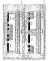
- FIGS. 9A-9Billustrate a 2D simulation of the doping profiles of structures utilizing several of the techniques of the present invention.
- FIG. 10provides a typical current vs. voltage (I-V) trace illustrating latch-up.
- FIG. 11illustrates I-V traces showing latch-up improvement associated with several of the techniques of the present invention.
- the devices and techniques described in the present applicationcan deliver a complete radiation solution, or in some cases a specialized radiation solution, by directly addressing one or more of the primary degradation radiation effects of ICs: Total Ionizing Dose (TID), Single Event Latch-up (SEL), and Single-Event Upset (SEU).
- TIDTotal Ionizing Dose
- SELSingle Event Latch-up
- SEUSingle-Event Upset
- the solutions to these degradation mechanismsare accomplished at the silicon process level with modifications to existing foundry baseline process.
- These unique approachescan be integrated into any CMOS process flow without affecting the performance of the underlying baseline technology.
- These approachescan further take advantage of a variety of different IC fabrication technologies, such as silicon-on-insulator (SOI) and the like.
- SOIsilicon-on-insulator
- the examples of the present applicationwill focus on MOS (and particularly CMOS) implementations, it will be understood by those having ordinary skill in the art that the devices and techniques disclosed herein can be extended to other semiconductor architecture
- This disclosuredescribes various structures and techniques that each generally provide some manner of protection from one or more of the degradation effects associated with radiation, and particularly ionizing radiation.
- these structures and techniquesprovide novel radiation hardened process isolation (RHPI) schemes.
- RHPIradiation hardened process isolation
- the RHPI structurescan significantly reduce the sensitivity of the silicon electrical devices to ionizing radiation, single event latch up, and single event soft error.
- the RHPI structurescan generally be applied to any MOS or BiCMOS silicon process and will directly improve radiation hardening properties of the integrated circuit both during and after exposure to a radiation environment. Moreover, this is accomplished with little or no penalty to circuit size and or electrical performance.
- the RHIP schemescan be used as an “add on” feature, which can be applied to existing MOS or BiCMOS process technology, improving radiation isolation properties without the need for extensive process or circuit changes.
- the RHPI structuresenable radiation hardening of commercial digital process by leveraging existing solid state processing technology and re-use of leading edge circuit IP for the creation of radiation hardened circuit product.
- Ionizing radiationoccurs naturally in the form of high-energy photons or charged particles that possess enough energy to break atomic bonds and create electron and hole pairs in an absorbing material. These particles can include protons, electrons, atomic ions, and photons with energies greater than a bandgap of the absorbing material.
- the ionizing radiationcan contribute to a total ionizing dose (TID).
- TIDtotal ionizing dose
- an ionizing particlepasses through a MOS device, it generates one or more electron-hole pairs which can be trapped in the gate oxides and the field oxides. Electrons in the semiconductor's valence band are raised to the conductor band.
- a fraction of the electron-hole pairswill undergo initial recombination and cause no damage, but such recombination decreases as the electric field increases, and the electrons and holes that survive it are free to diffuse and drift within the oxide where they will be swept from the insulator, recombine, or be trapped.
- Ionizing radiationalso boosts the interface trap density in MOS structures.
- Interface trapsare localized electronic states close to the interface between silicon and silicon dioxide and can exchange charge with the silicon conduction and valence bands. They shift threshold voltage and can also degrade mobility by acting as scattering centers. More specifically, the increase in interface states shifts the threshold voltages in the negative direction (more depletion V t ) for n-channel devices and in the positive direction (more enhancement V t ) for p-channel devices.
- threshold voltage shifts caused by ionizing radiationfurther affect parasitic MOS elements, giving rise, for example, to leakage currents that may cause parametric failure and/or functional failure.
- TIDEven more specialized devices can be susceptible to TID.
- SOI transistorscan also be affected by TID through charge buildup in the insulator such as a buried oxide.
- charge buildupcan invert the back surface causing a source-to-drain (back-channel) leakage current.
- this leakage currentrelatively unaffected by gate bias.
- back-channelsource-to-drain
- Positive oxide charge builduptends to deplete the back-channel interface causing a decrease in the threshold voltage of the front-channel gate oxide and increased back-channel leakage current.
- a wide variety of threshold voltage instabilitiescan result.
- the effects of ionizing radiationlead to the degradation of performance and ultimate failure of the CMOS devices.
- the additional radiation-induced interface statesdegrade the circuit performance by reducing the channel mobility, which as a result decreases channel conductance and transistor gain.
- the threshold voltages of the n-channel and p-channel devicesmay shift to such a degree where the n-channel transistors cannot be turned off and the drive capability of the p-channel transistors is not sufficient for the circuit to continue operating at the system clock rate.
- Such a shift in threshold voltages of either the n-channel or p-channel transistorscan cause a circuit to fail.
- FIGS. 1A-1Hillustrate one approach to addressing the parasitic effects associated with TID in a conventional MOS device.
- Transistor 100(shown in FIGS. 1 B and 1 D-H) differs from conventional MOS devices (shown in FIGS. 1A and 1C ) in that channel region 130 of transistor 100 includes two channel region extensions 135 .
- source ( 60 ), drain ( 70 ), and channel regions ( 80 )are typically fabricated to have approximately the same width as shown. However, as shown in FIGS.
- source region 110 and drain region 120have approximately the same widths while channel region 130 has a greater width leading to channel region extensions 135 that extend beyond the edges of the source and drain regions, i.e., beyond the channel region's typical interfaces with each of the source and drain regions.
- Channel region extensions 135are typically formed by an extension of the silicon active area from which the source, drain, and channel regions are formed, or by formation of mesa regions immediately adjacent to the channel region. Because of their role in reducing the parasitic effects associated with TID, these extended active area structures can be referred to as parasitic isolation devices (PIDs).
- PIDsparasitic isolation devices
- Each of channel region extensions 135have a width x and a length y ( FIG. 1E ). Although FIGS. 1 B and 1 D-H illustrate channel region extensions 135 having approximately the same dimensions as each other, this need not be the case.
- Channel region extension length yis typically smaller than the length of polysilicon gate 150 , while channel region extension width x can be selected to provide the desired device features.
- the increased length of the channel edge caused by the extensionsi.e., and increase from y to 2x+y, serves to increase the effective channel length of channel region 130 to a value greater than the case where the channel region terminates “flush” with source and drain regions 110 and 120 .
- channel region extensions 135lead to significantly reduced OFF state leakage due to the attenuation of parasitic transistor short channel effects.
- the PID structureeffectively increases the local channel length by more than a factor of two.
- the geometry of the PIDprovides for selective doping within specific regions 140 as shown in FIGS. 1F-1H .
- FIGS. 1F and 1Gshow top views of device 100 including channel extension impurity regions 140 , typically formed along the length of channel region extensions 135 .
- Channel extension impurity regions 140are typically formed to have relatively high impurity concentrations, and are introduced to overlap end portions of the channel region extensions so that the impurity concentration of these end portions is increased relative to the impurity concentration of those portions of the channel region 130 located between source region 110 and drain region 120 .
- channel extension impurity regions 140form a pair of p+ channel stops.
- This relatively high impurity concentration of the channel stopinsures that the parasitic sidewall threshold is higher than any negative threshold shift which might be induced by ionizing radiation.
- These more heavily doped extension impurity regionsare typically spaced apart from the endwall edges of source and drain regions 110 and 120 by respective portions of the extension regions of the same doping concentration as channel region 130 itself, so that the more heavily doped channel extension impurity regions do not form p+/n+ junctions with the source and drain regions 110 and 120 .
- Such junctionscan have very low breakdown voltages, thereby adversely effecting device performance.
- the extension width xis generally determined by the choice of doping ion and the manufacturing process's thermal diffusion exposure. For example, a boron doped PID structure would typically have a larger extension width x as compared to an Indium doped PID structure. Thus, extension width will typically be driven by concerns about excess back-diffusion and enhanced doping of the transistor active area. In general, either acceptor or donor impurities can be used to form channel extension impurity regions 140 . Variation of impurity type, implant energy, and dose will typically provide different types and/or levels of radiation isolation improvement.
- channel region extensions 135are located below (and hidden by) gate electrode 150 , which allows self aligned conventional processing to be used subsequent to PID formation.
- the channel region extensionswhen combined with impurity doping can be used to prevent unwanted electrical inversion (threshold voltage depletion) of the edges (or sides) of the n-channel transistor silicon channel area.
- This sensitive regiongenerally extends below the gate electrode between source region 110 and drain region 120 , as illustrated in FIG. 1H which shows an end view of the device.
- channel extension impurity regions 140are formed to extend to a depth greater than the depths of the source and drain regions.
- the PIDcan likewise be used in p-channel transistors to prevent threshold voltage enhancement (opposite of n-channel) caused by positive charge accumulation along the active area edge of the PMOS transistor active area.
- threshold voltage enhancementopposite of n-channel
- the PID structurecan increase the size of the transistors active area, gate capacitance may also increase. This can lead to reduced speed in operation of the transistor.
- various embodimentscan adjust different aspects of the device geometry. For example, in one embodiment the width of the PMOS can be increased to help reduce the gate capacitance.
- the PID structurereduces or eliminates parasitic field transistor inversion which reduces or eliminates a major source of I off leakage caused by charge build up at the silicon/SiO 2 ( 160 ) boundary.
- the PID structure doped regionprovides for local minority carrier lifetime reduction, reduced sensitivity to substrate noise and body voltage effects, and enhances the transistor snap-back voltage.
- the PID structures described hereincan be fabricated in both bulk silicon and silicon films, such as silicon-on-insulator (SOI).
- latch-upgenerally, and in the case of circuits in radiation environments SEL, is a serious failure mode in CMOS circuits. In the best case, latch-up results in soft failure with a loss of data or logic state. In the worst case, latch-up causes a destructive hard failure with permanent loss of the circuit. Thus, from a circuit reliability perspective, latch-up is to be avoided at all costs. As isolation widths shrink, device structures become even more susceptible to both latch-up failure modes. Prevention of both transient and destructive failures is very important in advanced CMOS IC's since most conventional CMOS technologies have largely converged on the use of p ⁇ bulk substrates. As noted above, radiation environments present special problems to CMOS circuits in that high-energy particles deposit significant electrical charge to the bulk substrate.
- the instantaneous appearance of static charge deposited by a high-energy particle passing through an ICcan immediately induce large displacement currents on the pico-second time scale accompanied with rapid potential shifts away from initial logic states.
- the deposition of energy by the particletypically causes diodes to forward bias, followed by large transient injection currents which reinforce the transient upset and can cause the CMOS circuit to latch-up.
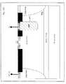
- FIG. 2shows a cross-section diagram of a CMOS inverter formed on a p ⁇ substrate. An equivalent circuit diagram is also shown in FIG. 2 overlaid on the CMOS inverter.
- the basic switching circuitis an inverter formed from a complementary pair of MOS transistors, one NMOS and one PMOS. Electrical isolation is achieved by using both dielectric and pn junction diodes. P-type doped regions (p-wells) isolate NMOS transistors, while n-typed doped regions (n-wells) isolate PMOS transistors.
- FIG. 2shows a cross-section diagram of a CMOS inverter formed on a p ⁇ substrate.
- An equivalent circuit diagramis also shown in FIG. 2 overlaid on the CMOS inverter.
- the basic switching circuitis an inverter formed from a complementary pair of MOS transistors, one NMOS and one PMOS. Electrical isolation is achieved by using both dielectric and pn junction diodes. P-type doped regions (p
- each MOSFET in the inverterforms bipolar emitters.
- the circuitmaintains a reverse bias of the diodes formed by the n-well/p-substrate, the p+/n ⁇ junction of the PMOS and the n+/p ⁇ junction of the NMOS.
- External factorssuch as leakage, circuit switching noise, particle upset, and transient overvoltage at the p+ diffusion or undervoltage at the n+ diffusion can trigger one of both of the parasitic bipolar devices into the active state. If either of the emitter or base junctions is forward biased, emitter currents will be sourced to corresponding base/collector regions, immediately shifting the local potential from its initial voltage state.
- the network parasitic devicesforms a pnpn silicon controlled rectifier (SCR) power device which can be unintentionally biased into a high current, low impedance state, thereby causing latch-up.
- the circuit elements R S1 , R S2 , and R S3are the net effective bulk p ⁇ substrate resistors, while R NW1 is the n-well series resistance and R PW1 is the p-well series resistance. In conventional technology substrate resistors would have resistances on the order of 1 k ⁇ or greater. In a typical example of CMOS circuit operation, the bulk substrate represents ground potential (0 volts) and is referred to as V SS .
- the local potential(within the p ⁇ substrate) will increase in magnitude above zero volts as function of the high value substrate resistance.
- forward biased p+/n ⁇ diffusion diodeswhich are located within the n-well isolation doping region that is caused by either an over voltage of the p+ diffusion or a transient under voltage condition existing within the n-well local potential, which typically equals the circuit supply voltage or terminal voltage (V DD , or V CC ).
- the network of series resistorsplays a direct role in the transient bias states of the different impurity doped regions, which then directly influences the bias and conduction state of the diodes. Latch-up can be prevented by keeping the diodes in their reversed bias (off) states.
- a first step in reducing or preventing latch-upis reducing the effective resistance of p ⁇ substrate resistors R S1 and R S2 .
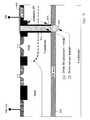
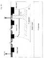
- the p ⁇ substrate resistancecan be reduced using a high-dose buried layer (HDBL) 300 as illustrated in FIG. 3 .
- HDBL layer 300is a heavily doped region of the same conductivity type as the p ⁇ substrate, and is placed beneath the active device regions of the device by ion implantation. In general, both the doping and damage characteristics of HDBL influence device performance.
- HDBL structuresare easily integrated into standard CMOS processing with the addition of typical steps such as, an implant step, a rapid thermal anneal (RTA), and an optional cleaning step in between the implant and anneal.
- RTArapid thermal anneal
- the process steps associated with the HDBLcan be performed either before or after dielectric isolation (SiO 2 ) formation either by LOCOS or the use of a shallow trench isolation (STI) structure common in many CMOS processes.
- SiO 2dielectric isolation
- STIshallow trench isolation
- Implanted dosestypically vary between 1 ⁇ 10 13 and 5 ⁇ 10 15 cm ⁇ 2 , which forms a highly doped and abrupt layer approximately 1.0-5.0 ⁇ m below the silicon surface.
- the buried layeris typically implanted sufficiently deep so that the final dopant profile (after all thermal processes) does not counterdope the retrograde well of opposite conductivity, which results in low well-substrate breakdown voltage.
- the deep p+ layerprovides a low resistance shunt 300 that significantly reduces the series resistance between the pnp subcollector (below the n-well) and the p+ collector (V SS ).
- Forming a p+ shunting layer 300 via implantationalso gives circuit designers the option of patterning the implant to independently optimize substrate resistivities in different areas, e.g., for a system-on-chip design.
- substrate resistors R S1 and R S2are now significantly reduced, typically by more than two orders of magnitude, because of the presence of HDBL 300 .
- the spreading resistance of the regioncan be lowered to less than 50 ⁇ as compared to 2 k ⁇ or more for conventional CMOS isolation.
- use of the HDBL alonedoes not effect other parasitic resistances such as R S3 and R PW1 . Consequently, significant vertical resistance continues to exist.
- a second step in addressing latch-up and other substrate current transientsis to reduce the significant vertical resistance.
- Addition of a vertical conductor 310 extending between the buried layer 300 and a p-well contact region (as shown) or some other substrate surface terminalsignificantly reduces this resistance.
- the vertical conductor 310is formed as a vertical impurity region having the same conductivity type as the substrate, but typically having an impurity concentration greater than that of the substrate.
- vertical conductor 310can be formed from one or more p+ implants into the region extending between p-well contact 320 and buried layer 300 .
- High-energy ion-implantation combined with photoresist masking and/or multiple energy implantationcan provide a vertical p+ doped region with high aspect ratio doping profile to bridge the uplink path from an ohmic V SS surface contact or Schottky diode to buried layer 300 or other p+ bulk layers as is typical fro p ⁇ epi on p+ bulk substrates.
- vertical conductor 310is formed by multiple ion-implant steps at one or more energy levels.
- a new structure referred to as a buried guard ringis formed.
- the BGRoffers several isolation attributes. Since the low resistance deep buried layer is now locally connected via a vertical doping region or other conductor: (1) minimum impedance is provided for most or all of the accumulated, deposited or injected charge occurring within the silicon substrate region; (2) transient times for charge termination are reduced thereby improving overall isolation by reducing or minimizing the duration of any n+/p ⁇ diode forward biasing which reduces injected currents; (3) the BGR forms a low-resistance circuit leg back to the p-well contact terminal, thereby creating a current divider which effectively shunts and sinks a majority of any injected or deposited current away from the R S4 and R S5 resistor legs, thereby significantly reducing base current feedback to the parasitic npn devices shown and limiting voltage transients for the p-bulk silicon region associated with the CMOS structure.
- the BGR structureby effectively shunting injected current or stray charge promptly to the V SS terminal, reduces or prevents voltage transients which could subsequently forward bias either or both of the n ⁇ /p ⁇ diodes (n-well/p-substrate diode inherent in CMOS twin well isolation) and the n+/p ⁇ diodes (inherent in NMOS transistor) and eliminates subsequent triggering of the pnpn SCR network. Latch-up the BGR isolation structure present then becomes difficult or impossible to initiate, thereby preserving the circuit from ever entering destructive latch-up.
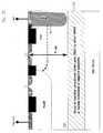
- FIG. 4illustrates and alternate implementation of the BGR structure.
- buried layer 400is connected to p-well contact 420 using an extended p-well area 410 as the vertical conductor.
- extended p-well area 410will typically extend well into buried layer 400 to ensure proper electrical contact.
- the vertical conductorcould be formed much the way vias or other vertical conductors are formed.
- a deep trench that terminates at or near the top of a buried layercould be used.
- silicide formation, and filling with polysilicon or metal, such a conductorcould extend to the substrate surface where it would be capped in a conventional manner and terminated as appropriate in a metallization scheme.
- Conductor formationcan also utilize emerging technologies, such as atomic layer deposition (ALD), or any other techniques as are well known by those having skill in the art.
- ALDatomic layer deposition
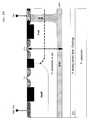
- FIG. 5illustrates an example of direct connection using a metallization scheme to contact HDBL horizontal layer 500 .
- shallow trench isolation (STI) structuresare used to insulate the vertical conductor from the surrounding p-well and substrate.
- STIshallow trench isolation
- a shallow trenchis etched into the substrate. The trench is then thermally oxidized and filled with a deposited oxide to make it non-conducting.
- Such a structureprovides good isolation between adjacent MOS devices.
- STI structure 505is extended down to buried layer 500 . Instead of filling STI structure with an insulative material, STI structure 505 includes an ohmic fill (e.g., polysilicon and/or metal) to proved the needed vertical conductor 510 .
- an ohmic fille.g., polysilicon and/or metal
- Ohmic contact implant 507is typically an ion implant extension extending from the bottom of the STI trench well into the buried layer.
- P-well contact 520is formed so as to be electrically coupled to vertical conductor 510 .
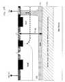
- FIGS. 6A-6Billustrate other implementations of the BGR structure.
- BGR structure 600formed using any of the structures/techniques described above
- the CMOS inverterare formed in p ⁇ epitaxial layer 630 which in turn is formed on n+ or n ⁇ bulk substrate 640 .
- various different techniquescan be used to form epitaxial layer 630 .
- FIG. 6Billustrates a BGR structure 650 (again, formed using any of the structures/techniques described above) formed along with the CMOS inverter in p ⁇ epitaxial layer 680 .
- Epitaxial layer 680is in turn formed on p+ bulk substrate 690 .
- FIGS. 7A-7Cillustrate still other embodiments and variations of the basic BGR structure.
- the BGR structureincludes only a vertical conductor 700 (e.g., a vertical doping structure, deposited conductor, etc.), and does not include the HDBL described above.
- a vertical conductor 700e.g., a vertical doping structure, deposited conductor, etc.
- Such an implementationcan provide adequate device benefits in some cases, particularly where the CMOS devices are very closely formed, such as in an SRAM implementation.
- BGR structure 700extends to the p+ or p ⁇ bulk silicon substrate 720 while passing through p ⁇ epi layer 710 , as would be used, for example, in a p-epi on p+ bulk wafer.
- Epitaxial layer 710is in turn formed on substrate 720 and contacted using only the vertical BGR extension 700 .
- FIG. 7Billustrates similar implementation, where vertical BGR component 730 is implemented into p ⁇ bulk silicon.
- FIG. 7Cshows an implementation where vertical BGR component 750 is formed in an epi layer 760 which in turn has beneath it a buried oxide layer 770 (or other SOI implementation) formed using well known SOI techniques.
- FIGS. 8A-8Eillustrate still other embodiments and variations of the basic BGR structure.
- BGR structure 800 and a corresponding CMOS inverterhave the same basic structure as that illustrated in FIG. 3 .
- the BGR structurecan in general be formed using any of the structures/techniques described above.
- an n-type doping layer 805is included beneath the buried layer portion of BGR 800 to act as a carrier recombination and/or gettering layer.
- Layer 805is typically left floating, i.e., it is not electrically coupled to ground or some other reference voltage. However, in other implementations, layer 805 can be coupled to a suitable potential.
- N-doped layer 805can be formed using any number of implant or diffusion techniques, as will be well known to those having ordinary skill in the art.
- devices using the BGR structurecan implemented in silicon on insulator (SOI) substrates in order to take advantage of the unique properties of such substrates.
- BGR structure 810 and its associated CMOS devicesare formed in epitaxial layer 815 .
- Buried oxide layer 820is formed in (e.g., using a separation by implantation of oxygen (SIMOX) process) or on (e.g., using a bonded wafer process) the bulk silicon wafer.
- SIMOXseparation by implantation of oxygen
- BGR devicescan further take advantage of the beneficial properties of SOI wafers including: reduced parasitic capacitance, additional SEU immunity, and in some cases simplified processing.
- FIG. 8Cillustrates an embodiment similar to that of FIG. 8B .
- BGR structure 825is formed from a single vertical conductive component as described above.
- BGR structure 825typically extends through the epi layer to approximately the depth of buried oxide layer 830 .
- BGR structure 825can stop well short of, or extend into buried oxide layer 830 .
- FIG. 8Dillustrates still another example where the BGR structure is used with a CMOS device that includes triple well isolation, common for many RF devices.
- BGR structure 835is formed within the p ⁇ substrate region 840 of the isolated p ⁇ well common to triple well isolation implementations, but still surrounded (on the sides) by the deep n-well structures and (below) by a buried n-layer used to provide the additional isolation.
- FIG. 8Eillustrates still another BGR embodiment where BGR structure 845 is formed from a single vertical conducting structure and no HDBL.
- BGR structure 845is implemented in the isolated p-well 850 of the triple well isolation structure.
- the final depth of the vertical BGR layeris consistent with the depth of the isolated p-well region and is typically less than 2 microns.
- FIGS. 9A-9Billustrate a 2D simulation (using the Taurus-Medici device simulation tool from Synopsys, Inc.) of the doping profile of a CMOS twin well structure with the heavily p+ doped region now extending below the V SS terminal to the p+ buried layer.
- FIG. 9Ashows the BGR structure emphasizing its connection to the V SS terminal, while FIG. 9B illustrates portions of the BGR structure under the device n-well.
- Contour 900shows the 1 ⁇ 10 18 cm 3 doping contour generally indicating the region of p+ doping that forms the BGR.
- Reference numbers 300 , 310 , and 320show the buried layer, vertical conductor, and p-well contact 320 respectively.
- the impurity concentration of the BGR regionsgenerally varies between 1 ⁇ 10 18 and 1 ⁇ 10 19 cm 3
- the p+ vertical doping regionis located only below the V SS terminal (the p-well connection region) so that it does not interfere with normal circuit operations.
- the improved contact to the HDBL shunt layeris shown to be extremely effective in preventing latch-up triggering.
- FIG. 10provides a typical current vs. voltage (I-V) trace illustrating latch-up as well as terms and features normally used in conjunction with a latch-up I-V trace.
- I-Vcurrent vs. voltage
- V BEFor overvoltages greater than 0.3 V higher than V DD , (V BE ) current is injected across the p+/n ⁇ emitter/base diode and collected in the base/collector junction. Once active, the pnp bipolar parasitic transistor actively injects current into the emitter base junction. The p+ emitter current is divided and flows to both the n-well base contact and the p+ collector (p-well). As the SCR trigger current is approached, pnp collector current is flowing to the V DD terminal within the n-well, and significant hole current is flowing to the V SS terminal which represents the pnp collector terminal.
- the n+/p ⁇ diode(which represents the emitter/base junction of the npn parasitic transistor) remains in the off state since, based on its local potential, it is still in a reversed biased blocking state.
- the vertical pnp(VPNP) will continue to inject holes into the p-substrate, which is terminated at the V SS (ground) body tie.
- the VPNP collector currentquickly drives the local potential in the p-well up from zero volts to +0.3 V above V SS , which then forward biases the n+/p ⁇ diode since the n+ diffusion potential is fixed at V SS .
- the electrons (minority carriers) injected into the p-wellwill be collected at the CMOS n-well, since this is the highest available local potential node.
- the n-wellis now acting as an npn sub-collector.
- the lateral npn (LNPN) collector currentnow provides significant current to the n-well base of the VPNP.
- LNPN collector currentflows across n-well series resistors ( FIG. 3 ). NPN collector current now flowing in the n-well forces an additional potential drop within the n-well (at the p+ diffusion) to some voltage below V DD . The point on the I-V plot in FIG.
- Trigger currentis a meaningful term by which to judge latchup resistance capability since it is a measure of the current necessary to shift the “net potential” to of the two independent diodes by +0.7 V. It is always desirable that the trigger current be as high as possible to prevent the pnpn from forward biasing to the low impedance non-blocking state.
- a transitional phase or negative resistanceoccurs once the trigger point is passed and the pnpn network transitions from the low current blocking state to the high current, low impedance state. Finally, the I-V curve reaches its minimum voltage value (vertical portion of FIG. 10 ). Just after the trigger point is passed, the current flowing between the two voltage rails (V DD and V SS ) moves from the substrate and n-well resistor to the surface, where the resistance is lowest. Even though the sheet resistances of the n-well and p-well regions along the edges of the STI are high, the spatial separation between the p+ diffusion (V DD ) and the n+ diffusions (V SS ) is small.
- the current flowing between V DD and V SShas now reached the lowest network resistance, and the associated voltage drop also reaches its minimum value.
- the aforementioned shunt resistorsdetermine how much current is retained in the network resistor legs, and any current remaining here is subtracted from the base currents of the VPNP and LNPN, decoupling the bipolar effectiveness. Latch-up that reaches this saturation stage will cause overheating and can melt both the silicon and metal regions from the heat generated by the large currents being passed.
- the holding voltageis the minimum voltage for which positive current feedback can be sustained by the VPNP and LNPN pair.
- FIG. 11illustrates the significant improvements made possible when BGR techniques are applied to a conventional CMOS isolation scheme.
- the lower curve 1100is a typical latch up I-V trace for an advanced CMOS technology with advanced n+/p+ spacing of 270 nm.
- the I-V traceshows that snap-back (latch-up failure) has occurred at approximately 200 ⁇ A/ ⁇ m, and the latch up holding voltage is approximately 1.2 V.
- the second curve 1110shows marked improvement associated with the presence of an HDBL, with snap-back now >500 ⁇ A/ ⁇ m and holding voltage approximately 1.4 V. However in both cases latch up has occurred with a holding voltage that is below the power supply of 1.5 V.
- the remaining curves 1120which represent IV characterization in the presence of a BGR structure show that no triggering event has occurred for even smaller n+/p+ spacing of 220 nm and with over voltage currents >1.6 mA/ ⁇ A/ ⁇ m.
- the lack of latch-up snap-back at these currentsmarks an improvement of more than 3 orders of magnitude.
- the simulation datashows the effectiveness of the BGR structure in preventing latch-up, even at extremely aggressive 220 nm n+/p+ spacing.
- the three dimensional heavily doped BGR layersextend both horizontally and vertically thus creating low ohmic regions of contiguous and/or connected to isolation doping regions which stand separated from the transistor doping regions.
- the BGR structurecan be integrated into any existing CMOS twin well isolation structure with no adverse impact to existing structures, thus enabling the improvements necessary to provide robust isolation for both conventional circuit noise initiated latch up and single event latch up.
- BGR structures and techniquescan be used to prevent latch-up in both radiation-hardened and conventional microelectronic circuits.
- BGR structures and techniquescan also be implemented on a variety of different process variations, such as epitaxial silicon on bulk silicon (either with or without a heavily doped substrate), SOI, SOS, and the like.
- the BGR structures and techniquescan also be used to reduce or eliminate both single-event upset (SEU) and single-event transient (SET) events.
- SEU and SETcan be caused by a high-energy particle, e.g., a single heavy ion or nuclear particle such as a neutron of alpha particle, passing through a critical node in an IC. Immediately after being struck by such a particle electrons and holes will be separated from the silicon lattice as a function of the particle's energy which is expressed as the linear energy transfer (LET Mev/mg-cm) of the particular particle. If the charge deposited and ultimately collected as free electrons and holes is greater than the critical charge of a memory cell or some other state-related device, a single-event upset can occur.
- a high-energy particlee.g., a single heavy ion or nuclear particle such as a neutron of alpha particle
- LET Mev/mg-cmlinear energy transfer
- the susceptibility of ICs to single-event upsetstypically depends on the amount of critical charge required to “flip” a bit and the probability that a particle with a LET large enough to deposit that critical charge will strike a sensitive node.
- the production of large numbers of electron/hole chargesalso creates a potential dipole within the particle track passing through the silicon material.
- the Hall effectsegregates the holes and electron charges to opposite sides of the electrostatic field.
- the positive chargescause the local potential of the p-substrate to increase in voltage to a positive value and continues to influence the local potential of the p ⁇ substrate positively for several nano-seconds after the high energy particle strike.
- SETsingle event transient
- CMOS logictypically uses inverter gates and cross coupled logic gates to store binary bits in any digital circuit
- the aforementioned BGR devices and techniqueswill prove useful in reducing SEU and SET.
- the BGR structureserves a similar role with regards to soft error as in the latch-up isolation. In both cases the BGR structure effectively sinks excess positive charge generated by the upset event, while maintaining node potential, and limiting the transient voltage swing and duration following an SEU, SEL, or SET event.
- Process and device simulationsare used to quantify the effectiveness of the BGR structure using what is known as mixed-mode simulation. Test cases for SEU upset have been simulated for heavy ions (krypton) with LET of 110 Mev/mg-cm.
- simulation studiesindicate that the BGR structure would significantly improve SEU and SET soft error when compared to conventional CMOS without BGR protection.
- the simulation studiesalso indicate that BGR effectiveness in reducing SEU events depends at least in part on the net resistance of the structure. For example, reducing the resistance of the HDBL in the BGR improved performance of the structure. Such resistance reduction can be optimized, for example, by using shallower HDBL implants, by increasing the implant dose, and/or by optimizing the vertical doping profile.
- any of several expressionsmay be equally well used when describing the operation of a circuit including the various signals and nodes within the circuit.
- Any kind of signalwhether a logic signal or a more general analog signal, takes the physical form of a voltage level (or for some circuit technologies, a current level) of a node within the circuit.
- Such shorthand phrases for describing circuit operation used hereinare more efficient to communicate details of circuit operation, particularly because the schematic diagrams in the figures clearly associate various signal names with the corresponding circuit blocks and nodes.
- IGFETinsulated gate field effect transistor
- IGFET transistorsare frequently discussed as having a drain, a gate, and a source, in most such devices the drain is interchangeable with the source. This is because the layout and semiconductor processing of the transistor is frequently symmetrical (which is typically not the case for bipolar transistors).
- the current handling terminal normally residing at the higher voltageis customarily called the drain.
- the current handling terminal normally residing at the lower voltageis customarily called the source.
- a sufficient voltage on the gatecauses a current to therefore flow from the drain to the source.
- the source voltage referred to in N-channel IGFET device equationsmerely refers to whichever drain or source terminal has the lower voltage at any given point in time.
- the “source” of the N-channel device of a bi-directional CMOS transfer gatedepends on which side of the transfer gate is at the lower voltage.
- the control terminalmay be deemed the gate
- the first current handling terminalmay be termed the “drain/source”
- the second current handling terminalmay be termed the “source/drain”.
- Such a descriptionis equally valid for a P-channel IGFET transistor, since the polarity between drain and source voltages, and the direction of current flow between drain and source, is not implied by such terminology.
- one current-handling terminalmay arbitrarily deemed the “drain” and the other deemed the “source”, with an implicit understanding that the two are not distinct, but interchangeable.
- IGFET transistorsare commonly referred to as MOSFET transistors (which literally is an acronym for “Metal-Oxide-Semiconductor Field Effect Transistor”), even though the gate material may be polysilicon or some material other than metal, and the dielectric may be oxynitride, nitride, or some material other than oxide.
- MOSFET transistorswhich literally is an acronym for “Metal-Oxide-Semiconductor Field Effect Transistor”
- MOSFET transistorswhich literally is an acronym for “Metal-Oxide-Semiconductor Field Effect Transistor”
- MOSFET transistorswhich literally is an acronym for “Metal-Oxide-Semiconductor Field Effect Transistor”
- MOSFET transistorswhich literally is an acronym for “Metal-Oxide-Semicon
- V DDa single positive power supply voltage (e.g., a 1.5 volt power supply) used to power a circuit is frequently named the “V DD ” power supply.
- transistors and other circuit elementsare actually connected to a V DD terminal or a V DD node, which is then operably connected to the V DD power supply.
- the colloquial use of phrases such as “tied to V DD ” or “connected to V DD ”is understood to mean “connected to the V DD node”, which is typically then operably connected to actually receive the V DD power supply voltage during use of the integrated circuit.
- V SSThe reference voltage for such a single power supply circuit is frequently called “V SS .”
- Transistors and other circuit elementsare actually connected to a V SS terminal or a V SS node, which is then operably connected to the V SS power supply during use of the integrated circuit.
- V SS terminalis connected to a ground reference potential, or just “ground.”
- the first power supply terminalis frequently named “V DD ”
- the second power supply terminalis frequently named “V SS .”
- V DDimplied a DC voltage connected to the drain terminal of an MOS transistor
- V SSimplied a DC voltage connected to the source terminal of an MOS transistor.
- V CCa historical term from bipolar circuits and frequently synonymous with a +5 volt power supply voltage, even when used with MOS transistors which lack collector terminals
- GNDground
- implementation of the disclosed devices and techniquesis not limited by CMOS technology, and thus implementations can utilize NMOS, PMOS, and various bipolar or other semiconductor fabrication technologies. While the disclosed devices and techniques have been described in light of the embodiments discussed above, one skilled in the art will also recognize that certain substitutions may be easily made in the circuits without departing from the teachings of this disclosure. Also, many circuits using NMOS transistors may be implemented using PMOS transistors instead, as is well known in the art, provided the logic polarity and power supply potentials are reversed. In this vein, the transistor conductivity type (i.e., N-channel or P-channel) within a CMOS circuit may be frequently reversed while still preserving similar or analogous operation. Moreover, other combinations of output stages are possible to achieve similar functionality.
Landscapes
- Engineering & Computer Science (AREA)
- Physics & Mathematics (AREA)
- Microelectronics & Electronic Packaging (AREA)
- General Physics & Mathematics (AREA)
- Computer Hardware Design (AREA)
- Condensed Matter Physics & Semiconductors (AREA)
- Power Engineering (AREA)
- Manufacturing & Machinery (AREA)
- Health & Medical Sciences (AREA)
- Electromagnetism (AREA)
- Toxicology (AREA)
- Metal-Oxide And Bipolar Metal-Oxide Semiconductor Integrated Circuits (AREA)
- Thin Film Transistor (AREA)
- Insulated Gate Type Field-Effect Transistor (AREA)
- Element Separation (AREA)
Abstract
Description
- This application claims the benefit, under 35 U.S.C. § 119 (e), of U.S. Provisional Application No. 60/545,271, filed Feb. 17, 2004, entitled “Buried Guard Ring And Radiation Hardened Isolation Structures And Fabrication Methods,” and naming Wesley H. Morris as the inventor. The above-referenced application is hereby incorporated by reference herein in their entirety.
- 1. Field of the Invention
- The present invention relates to integrated circuits, and particularly to integrated circuits with partial and/or complete immunity to failure modes associated with radiation exposure.
- 2. Description of the Related Art
- The high radiation environments, including the upper atmosphere, near-earth orbit, outer space, and certain terrestrial environments (e.g., proximity to devices producing significant amounts of radiation) provide the most hostile environments for reliable operation of microelectronic solid-state devices. Exposure to radiation causes electrical degradation of both transistors and circuit-isolation elements, which can lead to sporadic device behavior and/or complete destructive failure of integrated circuits (ICs). Because of the complexities of designing and fabricating integrated circuits tolerant of radiation environments, during the 1980s a number of large commercial semiconductor companies began to specialize in the production of radiation-hardened ICs, primarily for military and aerospace systems.
- At the same time, the high manufacturing costs of non-radiation-hardened commercial ICs has generally been offset by progress in high volume production, growing from less than $40B to more than $200B in 2004. To remain competitive, commercial IC manufacturers have deployed new state-of-the art silicon IC manufacturing facilities every 3-5 years.
- The more limited low-volume demand for radiation-hardened ICs cannot justify the expense of dedicated leading-edge manufacturing facilities, despite the very attractive margins in the military and aerospace electronics market. These financial constraints have severely limited the ability of radiation-hardened IC suppliers to utilize leading-edge IC manufacturing technology. Consequently, the number of companies producing radiation-hardened IC components has been dramatically reduced, and their capabilities have fallen far behind those of the commercial sector.
- During the 1990s, the combination of rising costs for new IC manufacturing facilities, military budget reductions, and a dwindling number of suppliers widened the technological disparity between commercial and radiation-hardened microelectronics. Commercial and military satellite manufacturers attempting to bridge this gap were forced to employ a new concept called “COTS” (commercial off-the-shelf) to procure the high-performance ICs required for building their electronic platforms.
- The COTS approach uses extensive laboratory testing of commodity (unhardened) commercial ICs to screen and “qualify” them for applications where they are likely to be exposed to damaging radiation. COTS was considered the only practical solution to obtain space-qualified high-performance ICs. Despite greatly diluted radiation standards, qualified product could not reliably be found using COTS. Therefore, those few nominally acceptable ICs typically offered no significant cost savings. Satellites manufactured using COTS ICs have suffered significant reductions in capability and mission lifetime due to destructive radiation exposure. The advancing miniaturization of CMOS technology increases sensitivity to certain forms of radiation, further widening the gap between COTS capabilities and space electronics market requirements. After more than ten years of system failures, the COTS approach has failed to provide a viable solution for the supply of radiation-hardened ICs.
- Accordingly, it is desirable to bring high-performance and cost-effective radiation-hardened integrated circuits (RHICs) to military, aerospace, and certain terrestrial electronics markets using the readily accessible leading-edge infrastructure of high-volume commercial microelectronics manufacturers. More specifically, it is further desirable to systematically address at the silicon process level each of the degradation mechanisms caused by radiation and to thereby develop new radiation hardened solutions that can be integrated into commercial microelectronic fabrication processes without impacting significantly the commercial baseline electrical spice parameters. This methodology offers the promise of circuit intellectual property (IP) re-use which would create new and distinct radiation hard circuit products from existing commercial circuit designs while avoiding costly circuit redesigns.
- It has been discovered that semiconductor devices can be fabricated using conventional designs and process but including specialized structures to reduce or eliminate detrimental effects caused by various forms of radiation. Such semiconductor devices can include the one or more parasitic isolation devices and/or buried guard ring structures disclosed in the present application. The introduction of design and/or process steps to accommodate these novel structures is compatible with conventional CMOS fabrication processes, and can therefore be accomplished at relatively low cost and with relative simplicity.
- Accordingly, one aspect of the present invention provides a semiconductor device including a substrate, a first well, a buried layer, and a vertical conductor. The substrate has a first conductivity type. The first well has the first conductivity type, and includes a first well contact region. The buried layer has the first conductivity type and is located beneath the first well. The buried layer further comprises a buried layer impurity concentration greater than a first substrate impurity concentration. The vertical conductor extends between the buried layer and one of the first well contact region and a substrate surface terminal.
- Another aspect of the present invention provides a method. A substrate having a first conductivity type is provided. The substrate includes a top surface. A layer is formed having the first conductivity type and located beneath the top surface of the substrate. The layer further comprises a layer impurity concentration greater than a first substrate impurity concentration. A first well region is formed between the layer and the top surface of the substrate. The first well region has the first conductivity type and includes a first well contact region. A vertical conductor is formed extending from the layer toward the top surface of the substrate.
- The foregoing is a summary and thus contains, by necessity, simplifications, generalizations and omissions of detail; consequently, those skilled in the art will appreciate that the summary is illustrative only and is not intended to be in any way limiting. As will also be apparent to one skilled in the art, the operations disclosed herein may be implemented in a number of ways, and such changes and modifications may be made without departing from this invention and its broader aspects. Other aspects, inventive features, and advantages of the present invention, as defined solely by the claims, will become apparent in the non-limiting detailed description set forth below.
- A more complete understanding of the present invention and advantages thereof may be acquired by referring to the following description and the accompanying drawings, in which like reference numbers indicate like features.
FIGS. 1A-1H illustrate simplified block diagrams of a transistor structure utilizing one of the techniques of the present invention.FIG. 2 shows a cross-section diagram of a CMOS inverter formed on a p-substrate.FIG. 3 illustrates a simplified block diagram of an inverter structure utilizing several of the techniques and devices of the present invention.FIG. 4 illustrates a simplified block diagram of an inverter structure utilizing additional techniques and devices of the present invention.FIG. 5 illustrates a simplified block diagram of an inverter structure utilizing still other techniques and devices of the present invention.FIGS. 6A-6B illustrate additional embodiments of the structure illustrated inFIG. 3 .FIGS. 7A-7C illustrate other embodiments of the present invention.FIGS. 8A-8E illustrate still other embodiments of the present invention.FIGS. 9A-9B illustrate a 2D simulation of the doping profiles of structures utilizing several of the techniques of the present invention.FIG. 10 provides a typical current vs. voltage (I-V) trace illustrating latch-up.FIG. 11 illustrates I-V traces showing latch-up improvement associated with several of the techniques of the present invention.- The following sets forth a detailed description of at least the best contemplated mode for carrying out the one or more devices and/or processes described herein. The description is intended to be illustrative and should not be taken to be limiting.
- The devices and techniques described in the present application can deliver a complete radiation solution, or in some cases a specialized radiation solution, by directly addressing one or more of the primary degradation radiation effects of ICs: Total Ionizing Dose (TID), Single Event Latch-up (SEL), and Single-Event Upset (SEU). Moreover, the solutions to these degradation mechanisms are accomplished at the silicon process level with modifications to existing foundry baseline process. These unique approaches can be integrated into any CMOS process flow without affecting the performance of the underlying baseline technology. These approaches can further take advantage of a variety of different IC fabrication technologies, such as silicon-on-insulator (SOI) and the like. Additionally, although the examples of the present application will focus on MOS (and particularly CMOS) implementations, it will be understood by those having ordinary skill in the art that the devices and techniques disclosed herein can be extended to other semiconductor architectures such as BiCMOS, etc.
- This disclosure describes various structures and techniques that each generally provide some manner of protection from one or more of the degradation effects associated with radiation, and particularly ionizing radiation. When combined, these structures and techniques provide novel radiation hardened process isolation (RHPI) schemes. When integrated into a CMOS process silicon structure, the RHPI structures can significantly reduce the sensitivity of the silicon electrical devices to ionizing radiation, single event latch up, and single event soft error. The RHPI structures can generally be applied to any MOS or BiCMOS silicon process and will directly improve radiation hardening properties of the integrated circuit both during and after exposure to a radiation environment. Moreover, this is accomplished with little or no penalty to circuit size and or electrical performance. As such, the RHIP schemes can be used as an “add on” feature, which can be applied to existing MOS or BiCMOS process technology, improving radiation isolation properties without the need for extensive process or circuit changes. The RHPI structures enable radiation hardening of commercial digital process by leveraging existing solid state processing technology and re-use of leading edge circuit IP for the creation of radiation hardened circuit product.
- Ionizing radiation occurs naturally in the form of high-energy photons or charged particles that possess enough energy to break atomic bonds and create electron and hole pairs in an absorbing material. These particles can include protons, electrons, atomic ions, and photons with energies greater than a bandgap of the absorbing material. When typical integrated circuits, such as the CMOS integrated circuits, are exposed to the charged particles over a period of months or even years, the ionizing radiation can contribute to a total ionizing dose (TID). For example, as an ionizing particle passes through a MOS device, it generates one or more electron-hole pairs which can be trapped in the gate oxides and the field oxides. Electrons in the semiconductor's valence band are raised to the conductor band. A fraction of the electron-hole pairs will undergo initial recombination and cause no damage, but such recombination decreases as the electric field increases, and the electrons and holes that survive it are free to diffuse and drift within the oxide where they will be swept from the insulator, recombine, or be trapped.
- Mobile electrons typically move through both gate and field oxides quickly, but the holes have a relatively low effective mobility and are easily trapped in gate oxides and field oxides. Because the trapped holes create a positive oxide charge, and the resulting space-charge fields cause negative shifts in the threshold voltages of corresponding transistors. As a threshold voltage shifts negatively, a transistor biased in the off-state lets more and more current pass. If enough holes are trapped, an n-channel transistor will remain fully conducting even with zero applied gate bias, causing, for example, an enhancement-mode device to become a depletion-mode device. In many cases, the edge or field region of the device becomes depletion-mode. Should that happen, leakage currents passing around a device (or from device to device) can cause parameter degradation and, ultimately, device and circuit failure.
- Ionizing radiation also boosts the interface trap density in MOS structures. Interface traps are localized electronic states close to the interface between silicon and silicon dioxide and can exchange charge with the silicon conduction and valence bands. They shift threshold voltage and can also degrade mobility by acting as scattering centers. More specifically, the increase in interface states shifts the threshold voltages in the negative direction (more depletion Vt) for n-channel devices and in the positive direction (more enhancement Vt) for p-channel devices. In addition to the positive oxide shift and the interface states shift described above with respect to n-channel and p-channel devices, threshold voltage shifts caused by ionizing radiation further affect parasitic MOS elements, giving rise, for example, to leakage currents that may cause parametric failure and/or functional failure.
- Even more specialized devices can be susceptible to TID. For example, SOI transistors can also be affected by TID through charge buildup in the insulator such as a buried oxide. For partially depleted transistors, charge buildup can invert the back surface causing a source-to-drain (back-channel) leakage current. Moreover, this leakage current relatively unaffected by gate bias. For fully-depleted transistors, there is significant sensitivity to radiation-induced oxide and interface-trap charge buildup. Positive oxide charge buildup tends to deplete the back-channel interface causing a decrease in the threshold voltage of the front-channel gate oxide and increased back-channel leakage current. Thus, a wide variety of threshold voltage instabilities can result.
- Thus, the effects of ionizing radiation lead to the degradation of performance and ultimate failure of the CMOS devices. The additional radiation-induced interface states degrade the circuit performance by reducing the channel mobility, which as a result decreases channel conductance and transistor gain. Over time, the threshold voltages of the n-channel and p-channel devices may shift to such a degree where the n-channel transistors cannot be turned off and the drive capability of the p-channel transistors is not sufficient for the circuit to continue operating at the system clock rate. Such a shift in threshold voltages of either the n-channel or p-channel transistors can cause a circuit to fail.
FIGS. 1A-1H illustrate one approach to addressing the parasitic effects associated with TID in a conventional MOS device. Transistor100 (shown in FIGS.1B and1D-H) differs from conventional MOS devices (shown inFIGS. 1A and 1C ) in thatchannel region 130 oftransistor 100 includes twochannel region extensions 135. In traditional MOS devices liketransistor 50, source (60), drain (70), and channel regions (80) are typically fabricated to have approximately the same width as shown. However, as shown in FIGS.1B and1D-H,source region 110 and drainregion 120 have approximately the same widths whilechannel region 130 has a greater width leading to channelregion extensions 135 that extend beyond the edges of the source and drain regions, i.e., beyond the channel region's typical interfaces with each of the source and drain regions.Channel region extensions 135 are typically formed by an extension of the silicon active area from which the source, drain, and channel regions are formed, or by formation of mesa regions immediately adjacent to the channel region. Because of their role in reducing the parasitic effects associated with TID, these extended active area structures can be referred to as parasitic isolation devices (PIDs).- Each of
channel region extensions 135 have a width x and a length y (FIG. 1E ). Although FIGS.1B and1D-H illustratechannel region extensions 135 having approximately the same dimensions as each other, this need not be the case. Channel region extension length y is typically smaller than the length ofpolysilicon gate 150, while channel region extension width x can be selected to provide the desired device features. The increased length of the channel edge caused by the extensions, i.e., and increase from y to 2x+y, serves to increase the effective channel length ofchannel region 130 to a value greater than the case where the channel region terminates “flush” with source and drainregions channel region extensions 135 lead to significantly reduced OFF state leakage due to the attenuation of parasitic transistor short channel effects. - In a typical implementation, the PID structure effectively increases the local channel length by more than a factor of two. The geometry of the PID provides for selective doping within
specific regions 140 as shown inFIGS. 1F-1H .FIGS. 1F and 1G show top views ofdevice 100 including channelextension impurity regions 140, typically formed along the length ofchannel region extensions 135. Channelextension impurity regions 140 are typically formed to have relatively high impurity concentrations, and are introduced to overlap end portions of the channel region extensions so that the impurity concentration of these end portions is increased relative to the impurity concentration of those portions of thechannel region 130 located betweensource region 110 and drainregion 120. For example, where the channel region has a p− impurity concentration, channelextension impurity regions 140 form a pair of p+ channel stops. This relatively high impurity concentration of the channel stop insures that the parasitic sidewall threshold is higher than any negative threshold shift which might be induced by ionizing radiation. These more heavily doped extension impurity regions are typically spaced apart from the endwall edges of source and drainregions channel region 130 itself, so that the more heavily doped channel extension impurity regions do not form p+/n+ junctions with the source and drainregions extension impurity regions 140. Variation of impurity type, implant energy, and dose will typically provide different types and/or levels of radiation isolation improvement. - As shown in
FIG. 1G ,channel region extensions 135 are located below (and hidden by)gate electrode 150, which allows self aligned conventional processing to be used subsequent to PID formation. In the case of n-channel devices, the channel region extensions when combined with impurity doping can be used to prevent unwanted electrical inversion (threshold voltage depletion) of the edges (or sides) of the n-channel transistor silicon channel area. This sensitive region generally extends below the gate electrode betweensource region 110 and drainregion 120, as illustrated inFIG. 1H which shows an end view of the device. Thus, in some embodiments, channelextension impurity regions 140 are formed to extend to a depth greater than the depths of the source and drain regions. The PID can likewise be used in p-channel transistors to prevent threshold voltage enhancement (opposite of n-channel) caused by positive charge accumulation along the active area edge of the PMOS transistor active area. Note that because the PID structure can increase the size of the transistors active area, gate capacitance may also increase. This can lead to reduced speed in operation of the transistor. To compensate for this effect, various embodiments can adjust different aspects of the device geometry. For example, in one embodiment the width of the PMOS can be increased to help reduce the gate capacitance. - Thus, the PID structure reduces or eliminates parasitic field transistor inversion which reduces or eliminates a major source of Ioffleakage caused by charge build up at the silicon/SiO2(160) boundary. Moreover, the PID structure doped region provides for local minority carrier lifetime reduction, reduced sensitivity to substrate noise and body voltage effects, and enhances the transistor snap-back voltage. The PID structures described herein can be fabricated in both bulk silicon and silicon films, such as silicon-on-insulator (SOI).
- Latch-up generally, and in the case of circuits in radiation environments SEL, is a serious failure mode in CMOS circuits. In the best case, latch-up results in soft failure with a loss of data or logic state. In the worst case, latch-up causes a destructive hard failure with permanent loss of the circuit. Thus, from a circuit reliability perspective, latch-up is to be avoided at all costs. As isolation widths shrink, device structures become even more susceptible to both latch-up failure modes. Prevention of both transient and destructive failures is very important in advanced CMOS IC's since most conventional CMOS technologies have largely converged on the use of p− bulk substrates. As noted above, radiation environments present special problems to CMOS circuits in that high-energy particles deposit significant electrical charge to the bulk substrate. The instantaneous appearance of static charge deposited by a high-energy particle passing through an IC can immediately induce large displacement currents on the pico-second time scale accompanied with rapid potential shifts away from initial logic states. The deposition of energy by the particle typically causes diodes to forward bias, followed by large transient injection currents which reinforce the transient upset and can cause the CMOS circuit to latch-up.
- Latch-up in a conventional CMOS inverter circuit is illustrated in
FIG. 2 .FIG. 2 shows a cross-section diagram of a CMOS inverter formed on a p− substrate. An equivalent circuit diagram is also shown inFIG. 2 overlaid on the CMOS inverter. In CMOS technology, the basic switching circuit is an inverter formed from a complementary pair of MOS transistors, one NMOS and one PMOS. Electrical isolation is achieved by using both dielectric and pn junction diodes. P-type doped regions (p-wells) isolate NMOS transistors, while n-typed doped regions (n-wells) isolate PMOS transistors.FIG. 2 illustrates the parasitic electrical elements, bipolar transistors, resistors and diodes, that co-exist within the CMOS structure. The source and drain regions of each MOSFET in the inverter form bipolar emitters. In normal operation, the circuit maintains a reverse bias of the diodes formed by the n-well/p-substrate, the p+/n− junction of the PMOS and the n+/p− junction of the NMOS. External factors such as leakage, circuit switching noise, particle upset, and transient overvoltage at the p+ diffusion or undervoltage at the n+ diffusion can trigger one of both of the parasitic bipolar devices into the active state. If either of the emitter or base junctions is forward biased, emitter currents will be sourced to corresponding base/collector regions, immediately shifting the local potential from its initial voltage state. - The network parasitic devices forms a pnpn silicon controlled rectifier (SCR) power device which can be unintentionally biased into a high current, low impedance state, thereby causing latch-up. The circuit elements RS1, RS2, and RS3are the net effective bulk p− substrate resistors, while RNW1is the n-well series resistance and RPW1is the p-well series resistance. In conventional technology substrate resistors would have resistances on the order of 1 kΩ or greater. In a typical example of CMOS circuit operation, the bulk substrate represents ground potential (0 volts) and is referred to as VSS. If current is injected from any source available to the p− substrate, the local potential (within the p− substrate) will increase in magnitude above zero volts as function of the high value substrate resistance. The n+/p− diffusion diodes located in the p-well, and which were previously undisturbed, would then enter a forward biased conduction as the P− substrate potential increases above approximately 0.3 volts. It is this second contribution by the previously undisturbed n+/p− diffusion diodes which now positively enhance the initial small signal upset event, and can lead to latch-up. Likewise the same event is possible starting with forward biased p+/n− diffusion diodes which are located within the n-well isolation doping region that is caused by either an over voltage of the p+ diffusion or a transient under voltage condition existing within the n-well local potential, which typically equals the circuit supply voltage or terminal voltage (VDD, or VCC).
- Thus, the network of series resistors plays a direct role in the transient bias states of the different impurity doped regions, which then directly influences the bias and conduction state of the diodes. Latch-up can be prevented by keeping the diodes in their reversed bias (off) states. A first step in reducing or preventing latch-up is reducing the effective resistance of p− substrate resistors RS1and RS2. The p− substrate resistance can be reduced using a high-dose buried layer (HDBL)300 as illustrated in
FIG. 3 . - In the example of
FIG. 3 ,HDBL layer 300 is a heavily doped region of the same conductivity type as the p− substrate, and is placed beneath the active device regions of the device by ion implantation. In general, both the doping and damage characteristics of HDBL influence device performance. HDBL structures are easily integrated into standard CMOS processing with the addition of typical steps such as, an implant step, a rapid thermal anneal (RTA), and an optional cleaning step in between the implant and anneal. The process steps associated with the HDBL can be performed either before or after dielectric isolation (SiO2) formation either by LOCOS or the use of a shallow trench isolation (STI) structure common in many CMOS processes. While a variety of different impurities can be used, the most common implants are boron implanted at 1.0-2.5 MeV (for p-type substrates), and phosphorus at 1.5-3.5 MeV (for n-type substrates). If a wafer-normal to ion implant beam angle of zero degrees is set during ion implantation, the necessary energy to achieve a desired depth of the ion implant can be significantly reduced. Implanted doses typically vary between 1×10¹³and 5×1015cm−2, which forms a highly doped and abrupt layer approximately 1.0-5.0 μm below the silicon surface. The buried layer is typically implanted sufficiently deep so that the final dopant profile (after all thermal processes) does not counterdope the retrograde well of opposite conductivity, which results in low well-substrate breakdown voltage. - For example, in the case of
FIG. 3 where the substrate is p− doped, the deep p+ layer provides alow resistance shunt 300 that significantly reduces the series resistance between the pnp subcollector (below the n-well) and the p+ collector (VSS). Forming ap+ shunting layer 300 via implantation also gives circuit designers the option of patterning the implant to independently optimize substrate resistivities in different areas, e.g., for a system-on-chip design. Thus, substrate resistors RS1and RS2are now significantly reduced, typically by more than two orders of magnitude, because of the presence ofHDBL 300. The spreading resistance of the region can be lowered to less than 50 Ω as compared to 2 kΩ or more for conventional CMOS isolation. However, use of the HDBL alone does not effect other parasitic resistances such as RS3and RPW1. Consequently, significant vertical resistance continues to exist. - A second step in addressing latch-up and other substrate current transients is to reduce the significant vertical resistance. Addition of a
vertical conductor 310 extending between the buriedlayer 300 and a p-well contact region (as shown) or some other substrate surface terminal significantly reduces this resistance. In one embodiment, thevertical conductor 310 is formed as a vertical impurity region having the same conductivity type as the substrate, but typically having an impurity concentration greater than that of the substrate. For example, where the substrate is a p− substrate,vertical conductor 310 can be formed from one or more p+ implants into the region extending between p-well contact 320 and buriedlayer 300. High-energy ion-implantation combined with photoresist masking and/or multiple energy implantation can provide a vertical p+ doped region with high aspect ratio doping profile to bridge the uplink path from an ohmic VSSsurface contact or Schottky diode to buriedlayer 300 or other p+ bulk layers as is typical fro p−epi on p+ bulk substrates. For example, in one implementationvertical conductor 310 is formed by multiple ion-implant steps at one or more energy levels. - When buried
layer 300 andvertical conductor 310 are used in conjunction with each other, a new structure referred to as a buried guard ring (BGR) is formed. The BGR offers several isolation attributes. Since the low resistance deep buried layer is now locally connected via a vertical doping region or other conductor: (1) minimum impedance is provided for most or all of the accumulated, deposited or injected charge occurring within the silicon substrate region; (2) transient times for charge termination are reduced thereby improving overall isolation by reducing or minimizing the duration of any n+/p− diode forward biasing which reduces injected currents; (3) the BGR forms a low-resistance circuit leg back to the p-well contact terminal, thereby creating a current divider which effectively shunts and sinks a majority of any injected or deposited current away from the RS4and RS5resistor legs, thereby significantly reducing base current feedback to the parasitic npn devices shown and limiting voltage transients for the p-bulk silicon region associated with the CMOS structure. The BGR structure, by effectively shunting injected current or stray charge promptly to the VSSterminal, reduces or prevents voltage transients which could subsequently forward bias either or both of the n−/p− diodes (n-well/p-substrate diode inherent in CMOS twin well isolation) and the n+/p− diodes (inherent in NMOS transistor) and eliminates subsequent triggering of the pnpn SCR network. Latch-up the BGR isolation structure present then becomes difficult or impossible to initiate, thereby preserving the circuit from ever entering destructive latch-up. FIG. 4 illustrates and alternate implementation of the BGR structure. In this example, buriedlayer 400 is connected to p-well contact 420 using an extended p-well area410 as the vertical conductor. Such an approach can potentially simplify device fabrication by making formation of the vertical conductor part of the normal p-well implant (or diffusion) process. Since the typical depth of buriedlayer 400 is from 1 to 5 μm, the p-well formation technique used should be capable of providing an adequately deep extended p-well. Moreover, extended p-well area410 will typically extend well into buriedlayer 400 to ensure proper electrical contact.- In still other examples, the vertical conductor could be formed much the way vias or other vertical conductors are formed. For example, a deep trench that terminates at or near the top of a buried layer could be used. With appropriate spacer formation, silicide formation, and filling with polysilicon or metal, such a conductor could extend to the substrate surface where it would be capped in a conventional manner and terminated as appropriate in a metallization scheme. Conductor formation can also utilize emerging technologies, such as atomic layer deposition (ALD), or any other techniques as are well known by those having skill in the art.
FIG. 5 illustrates an example of direct connection using a metallization scheme to contact HDBLhorizontal layer 500. In this example, shallow trench isolation (STI) structures are used to insulate the vertical conductor from the surrounding p-well and substrate. In a conventional STI structure, a shallow trench is etched into the substrate. The trench is then thermally oxidized and filled with a deposited oxide to make it non-conducting. Such a structure provides good isolation between adjacent MOS devices. However, in the example ofFIG. 5 ,STI structure 505 is extended down to buriedlayer 500. Instead of filling STI structure with an insulative material,STI structure 505 includes an ohmic fill (e.g., polysilicon and/or metal) to proved the needed vertical conductor510. Electrical contact between vertical conductor510 and buriedlayer 500 can be further enhanced using anohmic contact implant 507.Ohmic contact implant 507 is typically an ion implant extension extending from the bottom of the STI trench well into the buried layer. P-well contact 520 is formed so as to be electrically coupled to vertical conductor510.FIGS. 6A-6B illustrate other implementations of the BGR structure. InFIG. 6A , BGR structure600 (formed using any of the structures/techniques described above) and the CMOS inverter are formed in p−epitaxial layer 630 which in turn is formed on n+ or n−bulk substrate 640. As will be well known to those having ordinary skill in the art, various different techniques can be used to formepitaxial layer 630. Similarly,FIG. 6B illustrates a BGR structure650 (again, formed using any of the structures/techniques described above) formed along with the CMOS inverter in p−epitaxial layer 680.Epitaxial layer 680 is in turn formed onp+ bulk substrate 690.FIGS. 7A-7C illustrate still other embodiments and variations of the basic BGR structure. As shown inFIG. 7A , the BGR structure includes only a vertical conductor700 (e.g., a vertical doping structure, deposited conductor, etc.), and does not include the HDBL described above. Such an implementation can provide adequate device benefits in some cases, particularly where the CMOS devices are very closely formed, such as in an SRAM implementation. In this example,BGR structure 700 extends to the p+ or p−bulk silicon substrate 720 while passing through p− epi layer710, as would be used, for example, in a p-epi on p+ bulk wafer. Epitaxial layer710 is in turn formed onsubstrate 720 and contacted using only thevertical BGR extension 700.FIG. 7B illustrates similar implementation, wherevertical BGR component 730 is implemented into p− bulk silicon. Similarly,FIG. 7C shows an implementation wherevertical BGR component 750 is formed in anepi layer 760 which in turn has beneath it a buried oxide layer770 (or other SOI implementation) formed using well known SOI techniques.FIGS. 8A-8E illustrate still other embodiments and variations of the basic BGR structure. As shown inFIG. 8A ,BGR structure 800 and a corresponding CMOS inverter have the same basic structure as that illustrated inFIG. 3 . Note that in this example, as well as the examples ofFIGS. 8B-8E , the BGR structure can in general be formed using any of the structures/techniques described above. However, an n-type doping layer 805 is included beneath the buried layer portion ofBGR 800 to act as a carrier recombination and/or gettering layer.Layer 805 is typically left floating, i.e., it is not electrically coupled to ground or some other reference voltage. However, in other implementations,layer 805 can be coupled to a suitable potential. N-dopedlayer 805 can be formed using any number of implant or diffusion techniques, as will be well known to those having ordinary skill in the art.- As shown in
FIG. 8B , devices using the BGR structure can implemented in silicon on insulator (SOI) substrates in order to take advantage of the unique properties of such substrates. In this example, BGR structure810 and its associated CMOS devices are formed inepitaxial layer 815.Buried oxide layer 820 is formed in (e.g., using a separation by implantation of oxygen (SIMOX) process) or on (e.g., using a bonded wafer process) the bulk silicon wafer. Thus, BGR devices can further take advantage of the beneficial properties of SOI wafers including: reduced parasitic capacitance, additional SEU immunity, and in some cases simplified processing. FIG. 8C illustrates an embodiment similar to that ofFIG. 8B . However, in thiscase BGR structure 825 is formed from a single vertical conductive component as described above.BGR structure 825 typically extends through the epi layer to approximately the depth of buriedoxide layer 830. In some embodiments,BGR structure 825 can stop well short of, or extend into buriedoxide layer 830.FIG. 8D illustrates still another example where the BGR structure is used with a CMOS device that includes triple well isolation, common for many RF devices. Here,BGR structure 835 is formed within the p−substrate region 840 of the isolated p− well common to triple well isolation implementations, but still surrounded (on the sides) by the deep n-well structures and (below) by a buried n-layer used to provide the additional isolation.- Finally,
FIG. 8E illustrates still another BGR embodiment whereBGR structure 845 is formed from a single vertical conducting structure and no HDBL.BGR structure 845 is implemented in the isolated p-well850 of the triple well isolation structure. The final depth of the vertical BGR layer is consistent with the depth of the isolated p-well region and is typically less than 2 microns. FIGS. 9A-9B illustrate a 2D simulation (using the Taurus-Medici device simulation tool from Synopsys, Inc.) of the doping profile of a CMOS twin well structure with the heavily p+ doped region now extending below the VSSterminal to the p+ buried layer.FIG. 9A shows the BGR structure emphasizing its connection to the VSSterminal, whileFIG. 9B illustrates portions of the BGR structure under the device n-well.Contour 900 shows the 1×1018cm3doping contour generally indicating the region of p+ doping that forms the BGR.Reference numbers well contact 320 respectively. The impurity concentration of the BGR regions generally varies between 1×10¹⁸and 1×1019cm3In general, the p+ vertical doping region is located only below the VSSterminal (the p-well connection region) so that it does not interfere with normal circuit operations. As will be described below in connection withFIG. 11 , the improved contact to the HDBL shunt layer is shown to be extremely effective in preventing latch-up triggering.FIG. 10 provides a typical current vs. voltage (I-V) trace illustrating latch-up as well as terms and features normally used in conjunction with a latch-up I-V trace. In this example, the I-V characteristics of a p+ diffusion experiencing overvoltage are shown. The voltage at the p+ diffusion starts at VDD(1.5 V) and is ramped to higher voltage as would be the failure mode of an overvoltage condition. Since the p+ diffusion is diode isolated from the n-well, it can only block current up to the forward bias diode built-in potential of approximately +0.3 V before becoming active. For overvoltages greater than 0.3 V higher than VDD, (VBE) current is injected across the p+/n− emitter/base diode and collected in the base/collector junction. Once active, the pnp bipolar parasitic transistor actively injects current into the emitter base junction. The p+ emitter current is divided and flows to both the n-well base contact and the p+ collector (p-well). As the SCR trigger current is approached, pnp collector current is flowing to the VDDterminal within the n-well, and significant hole current is flowing to the VSSterminal which represents the pnp collector terminal. Note that prior to reaching the SCR trigger current, the n+/p− diode (which represents the emitter/base junction of the npn parasitic transistor) remains in the off state since, based on its local potential, it is still in a reversed biased blocking state.- If the overvoltage transient condition persists the vertical pnp (VPNP) will continue to inject holes into the p-substrate, which is terminated at the VSS(ground) body tie. The VPNP collector current quickly drives the local potential in the p-well up from zero volts to +0.3 V above VSS, which then forward biases the n+/p− diode since the n+ diffusion potential is fixed at VSS. This n+/p− diode, which has been inactive so far, now begins to inject electrons into the p− substrate as the potential of the p-well continues to increase. The electrons (minority carriers) injected into the p-well will be collected at the CMOS n-well, since this is the highest available local potential node. The n-well is now acting as an npn sub-collector. The lateral npn (LNPN) collector current now provides significant current to the n-well base of the VPNP. LNPN collector current flows across n-well series resistors (
FIG. 3 ). NPN collector current now flowing in the n-well forces an additional potential drop within the n-well (at the p+ diffusion) to some voltage below VDD. The point on the I-V plot inFIG. 10 that marks the transition of the pnpn from the high impedance (blocking) state to the negative differential resistance state is called the trigger current. Trigger current is a meaningful term by which to judge latchup resistance capability since it is a measure of the current necessary to shift the “net potential” to of the two independent diodes by +0.7 V. It is always desirable that the trigger current be as high as possible to prevent the pnpn from forward biasing to the low impedance non-blocking state. - A transitional phase or negative resistance occurs once the trigger point is passed and the pnpn network transitions from the low current blocking state to the high current, low impedance state. Finally, the I-V curve reaches its minimum voltage value (vertical portion of
FIG. 10 ). Just after the trigger point is passed, the current flowing between the two voltage rails (VDDand VSS) moves from the substrate and n-well resistor to the surface, where the resistance is lowest. Even though the sheet resistances of the n-well and p-well regions along the edges of the STI are high, the spatial separation between the p+ diffusion (VDD) and the n+ diffusions (VSS) is small. The current flowing between VDDand VSShas now reached the lowest network resistance, and the associated voltage drop also reaches its minimum value. The aforementioned shunt resistors determine how much current is retained in the network resistor legs, and any current remaining here is subtracted from the base currents of the VPNP and LNPN, decoupling the bipolar effectiveness. Latch-up that reaches this saturation stage will cause overheating and can melt both the silicon and metal regions from the heat generated by the large currents being passed. The holding voltage is the minimum voltage for which positive current feedback can be sustained by the VPNP and LNPN pair. - With this in mind,
FIG. 11 illustrates the significant improvements made possible when BGR techniques are applied to a conventional CMOS isolation scheme. Several curves are illustrated. Thelower curve 1100 is a typical latch up I-V trace for an advanced CMOS technology with advanced n+/p+ spacing of 270 nm. The I-V trace shows that snap-back (latch-up failure) has occurred at approximately 200 μA/μm, and the latch up holding voltage is approximately 1.2 V. Thesecond curve 1110 shows marked improvement associated with the presence of an HDBL, with snap-back now >500 μA/μm and holding voltage approximately 1.4 V. However in both cases latch up has occurred with a holding voltage that is below the power supply of 1.5 V. The remainingcurves 1120 which represent IV characterization in the presence of a BGR structure show that no triggering event has occurred for even smaller n+/p+ spacing of 220 nm and with over voltage currents >1.6 mA/μA/μm. The lack of latch-up snap-back at these currents marks an improvement of more than 3 orders of magnitude. The simulation data shows the effectiveness of the BGR structure in preventing latch-up, even at extremely aggressive 220 nm n+/p+ spacing. - The three dimensional heavily doped BGR layers extend both horizontally and vertically thus creating low ohmic regions of contiguous and/or connected to isolation doping regions which stand separated from the transistor doping regions. As can be seen in
FIGS. 3 and 9 A-9B, the BGR structure can be integrated into any existing CMOS twin well isolation structure with no adverse impact to existing structures, thus enabling the improvements necessary to provide robust isolation for both conventional circuit noise initiated latch up and single event latch up. Moreover, BGR structures and techniques can be used to prevent latch-up in both radiation-hardened and conventional microelectronic circuits. BGR structures and techniques can also be implemented on a variety of different process variations, such as epitaxial silicon on bulk silicon (either with or without a heavily doped substrate), SOI, SOS, and the like. - The BGR structures and techniques can also be used to reduce or eliminate both single-event upset (SEU) and single-event transient (SET) events. SEU and SET can be caused by a high-energy particle, e.g., a single heavy ion or nuclear particle such as a neutron of alpha particle, passing through a critical node in an IC. Immediately after being struck by such a particle electrons and holes will be separated from the silicon lattice as a function of the particle's energy which is expressed as the linear energy transfer (LET Mev/mg-cm) of the particular particle. If the charge deposited and ultimately collected as free electrons and holes is greater than the critical charge of a memory cell or some other state-related device, a single-event upset can occur. The susceptibility of ICs to single-event upsets typically depends on the amount of critical charge required to “flip” a bit and the probability that a particle with a LET large enough to deposit that critical charge will strike a sensitive node. The production of large numbers of electron/hole charges also creates a potential dipole within the particle track passing through the silicon material. The Hall effect segregates the holes and electron charges to opposite sides of the electrostatic field. Some electrons and holes can recombine in the lattice via SRH and Auger mechanisms. However, as a result of their higher mobility, electrons are quickly collected at the positive terminals, whereas the net concentration of holes, which have lower mobility and remain with the silicon body as static charge while unrecombined because of depleted electrons. The positive charges cause the local potential of the p-substrate to increase in voltage to a positive value and continues to influence the local potential of the p− substrate positively for several nano-seconds after the high energy particle strike. As a result of the potential upset within the p− substrate, other unstruck diodes are now activated which creates secondary currents and enhances the initial upset more significantly, an effect often referred to as single event transient (SET). While soft error results in data corruption, it is not destructive to the physical circuit.
- Since CMOS logic typically uses inverter gates and cross coupled logic gates to store binary bits in any digital circuit, the aforementioned BGR devices and techniques will prove useful in reducing SEU and SET. The BGR structure serves a similar role with regards to soft error as in the latch-up isolation. In both cases the BGR structure effectively sinks excess positive charge generated by the upset event, while maintaining node potential, and limiting the transient voltage swing and duration following an SEU, SEL, or SET event. Process and device simulations are used to quantify the effectiveness of the BGR structure using what is known as mixed-mode simulation. Test cases for SEU upset have been simulated for heavy ions (krypton) with LET of 110 Mev/mg-cm. In these simulations, where an inverter is brought to either a digital “one” state or a digital “zero” state and the mixed-mode SEU simulation is executed. In 21 different cases (21 different ion strike points, or angles of strike), the conventional CMOS inverter was shown to fail, i.e., an SEU occurred 9 times out of 21, or 43% of the time. In the simulations, the SEU charge transfer is completed within by 50 ps of the event, however the simulation was continued to 1 ns to observe charge recovery and circuit response.
- Results from the same simulations using a CMOS inverter with a similar structure but now including the aforementioned BGR structure show marked improvement. In this example, there are no failures in the same 21 cases. While the BGR structure demonstrated no failure in 21 SEU tests, the contrast with the bulk silicon simulations is even more significant. In several cases of the BGR structure simulations, significant improvement both in voltage stability and transient response were seen. The BGR structures, when compared to the bulk example, appear to “clamp” the node potential for certain SEU strikes and completely eliminates the possibility of secondary injection by the unstruck nodes since the p− substrate potential is maintained at or very near zero during SEU events. Moreover, simulation studies indicate that the BGR structure would significantly improve SEU and SET soft error when compared to conventional CMOS without BGR protection. The simulation studies also indicate that BGR effectiveness in reducing SEU events depends at least in part on the net resistance of the structure. For example, reducing the resistance of the HDBL in the BGR improved performance of the structure. Such resistance reduction can be optimized, for example, by using shallower HDBL implants, by increasing the implant dose, and/or by optimizing the vertical doping profile.
- Regarding terminology used herein, it will be appreciated by one skilled in the art that any of several expressions may be equally well used when describing the operation of a circuit including the various signals and nodes within the circuit. Any kind of signal, whether a logic signal or a more general analog signal, takes the physical form of a voltage level (or for some circuit technologies, a current level) of a node within the circuit. Such shorthand phrases for describing circuit operation used herein are more efficient to communicate details of circuit operation, particularly because the schematic diagrams in the figures clearly associate various signal names with the corresponding circuit blocks and nodes.
- An insulated gate field effect transistor (IGFET) may be conceptualized as having a control terminal which controls the flow of current between a first current handling terminal and a second current handling terminal. Although IGFET transistors are frequently discussed as having a drain, a gate, and a source, in most such devices the drain is interchangeable with the source. This is because the layout and semiconductor processing of the transistor is frequently symmetrical (which is typically not the case for bipolar transistors). For an N-channel IGFET transistor, the current handling terminal normally residing at the higher voltage is customarily called the drain. The current handling terminal normally residing at the lower voltage is customarily called the source. A sufficient voltage on the gate (relative to the source voltage) causes a current to therefore flow from the drain to the source. The source voltage referred to in N-channel IGFET device equations merely refers to whichever drain or source terminal has the lower voltage at any given point in time. For example, the “source” of the N-channel device of a bi-directional CMOS transfer gate depends on which side of the transfer gate is at the lower voltage. To reflect this symmetry of most N-channel IGFET transistors, the control terminal may be deemed the gate, the first current handling terminal may be termed the “drain/source”, and the second current handling terminal may be termed the “source/drain”. Such a description is equally valid for a P-channel IGFET transistor, since the polarity between drain and source voltages, and the direction of current flow between drain and source, is not implied by such terminology. Alternatively, one current-handling terminal may arbitrarily deemed the “drain” and the other deemed the “source”, with an implicit understanding that the two are not distinct, but interchangeable. It should be noted that IGFET transistors are commonly referred to as MOSFET transistors (which literally is an acronym for “Metal-Oxide-Semiconductor Field Effect Transistor”), even though the gate material may be polysilicon or some material other than metal, and the dielectric may be oxynitride, nitride, or some material other than oxide. The casual use of such historical legacy terms as MOS and MOSFET should not only be interpreted to literally specify a metal gate FET having an oxide dielectric.
- Regarding power supplies, a single positive power supply voltage (e.g., a 1.5 volt power supply) used to power a circuit is frequently named the “VDD” power supply. In an integrated circuit, transistors and other circuit elements are actually connected to a VDDterminal or a VDDnode, which is then operably connected to the VDDpower supply. The colloquial use of phrases such as “tied to VDD” or “connected to VDD” is understood to mean “connected to the VDDnode”, which is typically then operably connected to actually receive the VDDpower supply voltage during use of the integrated circuit. The reference voltage for such a single power supply circuit is frequently called “VSS.” Transistors and other circuit elements are actually connected to a VSSterminal or a VSSnode, which is then operably connected to the VSSpower supply during use of the integrated circuit. Frequently the VSSterminal is connected to a ground reference potential, or just “ground.” Generalizing somewhat, the first power supply terminal is frequently named “VDD”, and the second power supply terminal is frequently named “VSS.” Historically the nomenclature “VDD” implied a DC voltage connected to the drain terminal of an MOS transistor and VSSimplied a DC voltage connected to the source terminal of an MOS transistor. For example, old PMOS circuits used a negative VDDpower supply, while old NMOS circuits used a positive VDDpower supply. Common usage, however, frequently ignores this legacy and uses VDDfor the more positive supply voltage and VSSfor the more negative (or ground) supply voltage unless, of course, defined otherwise. Describing a circuit as functioning with a “VDDsupply” and “ground” does not necessarily mean the circuit cannot function using other power supply potentials. Other common power supply terminal names are “VCC” (a historical term from bipolar circuits and frequently synonymous with a +5 volt power supply voltage, even when used with MOS transistors which lack collector terminals) and “GND” or just “ground.”
- Moreover, implementation of the disclosed devices and techniques is not limited by CMOS technology, and thus implementations can utilize NMOS, PMOS, and various bipolar or other semiconductor fabrication technologies. While the disclosed devices and techniques have been described in light of the embodiments discussed above, one skilled in the art will also recognize that certain substitutions may be easily made in the circuits without departing from the teachings of this disclosure. Also, many circuits using NMOS transistors may be implemented using PMOS transistors instead, as is well known in the art, provided the logic polarity and power supply potentials are reversed. In this vein, the transistor conductivity type (i.e., N-channel or P-channel) within a CMOS circuit may be frequently reversed while still preserving similar or analogous operation. Moreover, other combinations of output stages are possible to achieve similar functionality.
- Although the present invention has been described with respect to a specific preferred embodiment thereof, various changes and modifications may be suggested to one skilled in the art and it is intended that the present invention encompass such changes and modifications that fall within the scope of the appended claims.
Claims (52)
Priority Applications (10)
| Application Number | Priority Date | Filing Date | Title |
|---|---|---|---|
| US10/951,283US7304354B2 (en) | 2004-02-17 | 2004-09-27 | Buried guard ring and radiation hardened isolation structures and fabrication methods |
| EP05713574AEP1716591A4 (en) | 2004-02-17 | 2005-02-15 | ENCAPED GUARD RING, RADIATION ISOLATION STRUCTURES, AND METHODS OF MANUFACTURING THE SAME |
| PCT/US2005/004740WO2005079400A2 (en) | 2004-02-17 | 2005-02-15 | Buried guard ring and radiation hardened isolation structures and fabrication methods |
| JP2006553340AJP2007523481A (en) | 2004-02-17 | 2005-02-15 | Embedded guard ring, radiation-resistant separation structure and manufacturing method thereof |
| US11/486,347US7804138B2 (en) | 2004-02-17 | 2006-07-13 | Buried guard ring and radiation hardened isolation structures and fabrication methods |
| US11/949,708US8093145B2 (en) | 2004-02-17 | 2007-12-03 | Methods for operating and fabricating a semiconductor device having a buried guard ring structure |
| US11/949,654US7629654B2 (en) | 2004-02-17 | 2007-12-03 | Buried guard ring structures and fabrication methods |
| US13/346,319US8497195B2 (en) | 2004-02-17 | 2012-01-09 | Method for radiation hardening a semiconductor device |
| JP2012129441AJP5607111B2 (en) | 2004-02-17 | 2012-06-07 | Embedded guard ring, radiation-resistant separation structure and manufacturing method thereof |
| US13/953,625US8729640B2 (en) | 2004-02-17 | 2013-07-29 | Method and structure for radiation hardening a semiconductor device |
Applications Claiming Priority (2)
| Application Number | Priority Date | Filing Date | Title |
|---|---|---|---|
| US54527104P | 2004-02-17 | 2004-02-17 | |
| US10/951,283US7304354B2 (en) | 2004-02-17 | 2004-09-27 | Buried guard ring and radiation hardened isolation structures and fabrication methods |
Related Child Applications (3)
| Application Number | Title | Priority Date | Filing Date |
|---|---|---|---|
| US11/486,347ContinuationUS7804138B2 (en) | 2004-02-17 | 2006-07-13 | Buried guard ring and radiation hardened isolation structures and fabrication methods |
| US11/949,708ContinuationUS8093145B2 (en) | 2004-02-17 | 2007-12-03 | Methods for operating and fabricating a semiconductor device having a buried guard ring structure |
| US11/949,654ContinuationUS7629654B2 (en) | 2004-02-17 | 2007-12-03 | Buried guard ring structures and fabrication methods |
Publications (2)
| Publication Number | Publication Date |
|---|---|
| US20050179093A1true US20050179093A1 (en) | 2005-08-18 |
| US7304354B2 US7304354B2 (en) | 2007-12-04 |
Family
ID=34841218
Family Applications (6)
| Application Number | Title | Priority Date | Filing Date |
|---|---|---|---|
| US10/951,283Expired - LifetimeUS7304354B2 (en) | 2004-02-17 | 2004-09-27 | Buried guard ring and radiation hardened isolation structures and fabrication methods |
| US11/486,347Active2027-07-08US7804138B2 (en) | 2004-02-17 | 2006-07-13 | Buried guard ring and radiation hardened isolation structures and fabrication methods |
| US11/949,708Active2027-09-03US8093145B2 (en) | 2004-02-17 | 2007-12-03 | Methods for operating and fabricating a semiconductor device having a buried guard ring structure |
| US11/949,654Expired - LifetimeUS7629654B2 (en) | 2004-02-17 | 2007-12-03 | Buried guard ring structures and fabrication methods |
| US13/346,319Expired - Fee RelatedUS8497195B2 (en) | 2004-02-17 | 2012-01-09 | Method for radiation hardening a semiconductor device |
| US13/953,625Expired - LifetimeUS8729640B2 (en) | 2004-02-17 | 2013-07-29 | Method and structure for radiation hardening a semiconductor device |
Family Applications After (5)
| Application Number | Title | Priority Date | Filing Date |
|---|---|---|---|
| US11/486,347Active2027-07-08US7804138B2 (en) | 2004-02-17 | 2006-07-13 | Buried guard ring and radiation hardened isolation structures and fabrication methods |
| US11/949,708Active2027-09-03US8093145B2 (en) | 2004-02-17 | 2007-12-03 | Methods for operating and fabricating a semiconductor device having a buried guard ring structure |
| US11/949,654Expired - LifetimeUS7629654B2 (en) | 2004-02-17 | 2007-12-03 | Buried guard ring structures and fabrication methods |
| US13/346,319Expired - Fee RelatedUS8497195B2 (en) | 2004-02-17 | 2012-01-09 | Method for radiation hardening a semiconductor device |
| US13/953,625Expired - LifetimeUS8729640B2 (en) | 2004-02-17 | 2013-07-29 | Method and structure for radiation hardening a semiconductor device |
Country Status (4)
| Country | Link |
|---|---|
| US (6) | US7304354B2 (en) |
| EP (1) | EP1716591A4 (en) |
| JP (2) | JP2007523481A (en) |
| WO (1) | WO2005079400A2 (en) |
Cited By (48)
| Publication number | Priority date | Publication date | Assignee | Title |
|---|---|---|---|---|
| US20060001121A1 (en)* | 2004-07-05 | 2006-01-05 | Dongbuanam Semiconductor Inc. | Phototransistor of CMOS image sensor and method for fabricating the same |
| US20060113599A1 (en)* | 2004-09-24 | 2006-06-01 | Jae-Hun Jeong | Semiconductor devices having self-aligned bodies and methods of forming the same |
| US20060150128A1 (en)* | 2005-01-06 | 2006-07-06 | Texas Instruments, Incorporated | Method of fabricating and integrated circuit to improve soft error performance |
| DE102005042868A1 (en)* | 2005-09-08 | 2007-03-29 | Infineon Technologies Ag | Field effect power component comprises a field effect element and an integral complementary metal oxide semiconductor structure surrounded by an outer trench structure |
| US20070096255A1 (en)* | 2004-04-12 | 2007-05-03 | System General Corp. | High resistance cmos resistor |
| WO2007061531A2 (en) | 2005-10-14 | 2007-05-31 | Silicon Space Technology Corporation | Radiation hardened isolation structures and fabrication methods |
| US20070164443A1 (en)* | 2005-09-29 | 2007-07-19 | Atmel Germany Gmbh | Semiconductor array and method for manufacturing a semiconductor array |
| US20070195841A1 (en)* | 2006-02-21 | 2007-08-23 | Aitken John M | Charge neutralization in semiconductor structures |
| US7298010B1 (en) | 2006-02-21 | 2007-11-20 | Sandia Corporation | Radiation-hardened transistor and integrated circuit |
| US20070278612A1 (en)* | 2006-05-31 | 2007-12-06 | Advanced Analogic Technologies, Inc. | Isolation structures for integrated circuits and modular methods of forming the same |
| US20080077376A1 (en)* | 2006-09-25 | 2008-03-27 | Iroc Technologies | Apparatus and method for the determination of SEU and SET disruptions in a circuit caused by ionizing particle strikes |
| WO2008019329A3 (en)* | 2006-08-04 | 2008-04-03 | Silicon Space Technology Corp | Improved radiation immunity of integrated circuits using backside die contact and electrically conductive layers |
| US20080197446A1 (en)* | 2002-08-14 | 2008-08-21 | Advanced Analogic Technologies, Inc. | Isolated diode |
| US20080197408A1 (en)* | 2002-08-14 | 2008-08-21 | Advanced Analogic Technologies, Inc. | Isolated quasi-vertical DMOS transistor |
| CN100416799C (en)* | 2005-11-30 | 2008-09-03 | 奇景光电股份有限公司 | Triple operating voltage device |
| US20080213972A1 (en)* | 2002-08-14 | 2008-09-04 | Advanced Analogic Technologies, Inc. | Processes for forming isolation structures for integrated circuit devices |
| US20080210980A1 (en)* | 2002-08-14 | 2008-09-04 | Advanced Analogic Technologies, Inc. | Isolated CMOS transistors |
| US20080217699A1 (en)* | 2002-08-14 | 2008-09-11 | Advanced Analogic Technologies, Inc. | Isolated Bipolar Transistor |
| US20080237782A1 (en)* | 2007-03-28 | 2008-10-02 | Advanced Analogic Technologies, Inc. | Isolated rectifier diode |
| US20080237704A1 (en)* | 2007-03-28 | 2008-10-02 | Advanced Analogic Technologies, Inc. | Isolated trench MOSFET |
| US20090072313A1 (en)* | 2007-09-19 | 2009-03-19 | International Business Machines Corporation | Hardened transistors in soi devices |
| US20090194843A1 (en)* | 2008-02-01 | 2009-08-06 | Infineon Technologies Ag | Integrated circuit arrangement including a protective structure |
| US20100034000A1 (en)* | 2008-07-04 | 2010-02-11 | Stmicroelectronics (Rousset) Sas | Electronic circuit having a diode-connected mos transistor with an improved efficiency |
| US20100133611A1 (en)* | 2002-08-14 | 2010-06-03 | Advanced Analogic Technologies, Inc. | Isolated transistor |
| US20100156511A1 (en)* | 2008-12-23 | 2010-06-24 | International Business Machines Corporation | Bias voltage generation circuit for an soi radio frequency switch |
| US20100237389A1 (en)* | 2009-03-20 | 2010-09-23 | International Business Machines Corporation | Design structure for heavy ion tolerant device, method of manufacturing the same and structure thereof |
| US20110102042A1 (en)* | 2007-09-19 | 2011-05-05 | International Business Machines Corporation | Apparatus and method for hardening latches in soi cmos devices |
| US7956391B2 (en) | 2002-08-14 | 2011-06-07 | Advanced Analogic Technologies, Inc. | Isolated junction field-effect transistor |
| US20110201171A1 (en)* | 2002-08-14 | 2011-08-18 | Advanced Analogic Technologies, Inc. | Processes For Forming Isolation Structures For Integrated Circuit Devices |
| US20120292733A1 (en)* | 2010-01-21 | 2012-11-22 | Fudan University | Mixed Schottky/P-N Junction Diode and Method of Making |
| US20130105904A1 (en)* | 2011-11-01 | 2013-05-02 | Texas Instruments Incorporated | Radiation hardened integrated circuit |
| US8587071B2 (en)* | 2012-04-23 | 2013-11-19 | Taiwan Semiconductor Manufacturing Co., Ltd. | Electrostatic discharge (ESD) guard ring protective structure |
| US8686531B2 (en) | 2007-11-19 | 2014-04-01 | Fairchild Korea Semiconductor, Ltd. | Structure and method for forming a guard ring to protect a control device in a power semiconductor IC |
| US20150222317A1 (en)* | 2014-02-05 | 2015-08-06 | Infineon Technologies Ag | Switching device, a communication device, and a method for processing a carrier |
| US9263447B2 (en)* | 2014-06-11 | 2016-02-16 | Nuvoton Technology Corporation | Semiconductor device |
| US20160343769A1 (en)* | 2013-05-14 | 2016-11-24 | Fermi Research Alliance LLC. | Monolithic active pixel radiation detector with shielding techniques |
| US10186514B1 (en) | 2017-09-06 | 2019-01-22 | Qualcomm Incorporated | Bi-stable static random access memory (SRAM) bit cells formed from III-V compounds and configured to achieve higher operating speeds |
| US10312244B2 (en)* | 2017-09-19 | 2019-06-04 | Qualcomm Incorporated | Bi-stable static random access memory (SRAM) bit cells that facilitate direct writing for storage |
| US10418402B2 (en)* | 2017-11-30 | 2019-09-17 | Stmicroelectronics (Research & Development) Limited | Near ultraviolet photocell |
| CN111739838A (en)* | 2020-06-23 | 2020-10-02 | 中国科学院上海微系统与信息技术研究所 | A kind of preparation method of radiation-resistant SOI material |
| US11037927B2 (en) | 2013-03-04 | 2021-06-15 | Seiko Epson Corporation | Circuit device and electronic apparatus |
| US11201245B2 (en)* | 2005-07-11 | 2021-12-14 | Psemi Corporation | Method and apparatus improving gate oxide reliability by controlling accumulated charge |
| US11206017B2 (en) | 2001-10-10 | 2021-12-21 | Psemi Corporation | Switch circuit and method of switching radio frequency signals |
| US20220093527A1 (en)* | 2019-01-10 | 2022-03-24 | Samsung Electronics Co., Ltd. | Integrated circuit chip, integrated circuit package and display apparatus including the integrated circuit chip |
| US20230118158A1 (en)* | 2020-02-18 | 2023-04-20 | Robert Bosch Gmbh | Vertical fin field effect transistor, vertical fin field effect transistor arrangement, and method for forming a vertical fin field effect transistor |
| CN116113309A (en)* | 2023-04-13 | 2023-05-12 | 南京邮电大学 | Low-offset Hall device adopting double protection rings and application method thereof |
| US11695407B2 (en) | 2005-07-11 | 2023-07-04 | Psemi Corporation | Circuit and method for controlling charge injection in radio frequency switches |
| US12074217B2 (en) | 2005-07-11 | 2024-08-27 | Psemi Corporation | Method and apparatus for use in improving linearity of MOSFETs using an accumulated charge sink-harmonic wrinkle reduction |
Families Citing this family (64)
| Publication number | Priority date | Publication date | Assignee | Title |
|---|---|---|---|---|
| US7304354B2 (en) | 2004-02-17 | 2007-12-04 | Silicon Space Technology Corp. | Buried guard ring and radiation hardened isolation structures and fabrication methods |
| US7605429B2 (en)* | 2005-04-15 | 2009-10-20 | International Business Machines Corporation | Hybrid crystal orientation CMOS structure for adaptive well biasing and for power and performance enhancement |
| US8110868B2 (en)* | 2005-07-27 | 2012-02-07 | Infineon Technologies Austria Ag | Power semiconductor component with a low on-state resistance |
| US8461648B2 (en)* | 2005-07-27 | 2013-06-11 | Infineon Technologies Austria Ag | Semiconductor component with a drift region and a drift control region |
| JP5003856B2 (en)* | 2005-10-21 | 2012-08-15 | セイコーエプソン株式会社 | Semiconductor device |
| US20070145367A1 (en)* | 2005-12-27 | 2007-06-28 | Taiwan Semiconductor Manufacturing Company, Ltd. | Three-dimensional integrated circuit structure |
| US7772648B1 (en)* | 2006-09-13 | 2010-08-10 | Rf Micro Devices, Inc. | Performance enhanced silicon-on-insulator technology |
| US7666750B2 (en)* | 2006-09-13 | 2010-02-23 | Agere Systems Inc. | Bipolar device having improved capacitance |
| US7462885B2 (en)* | 2006-11-30 | 2008-12-09 | Taiwan Semiconductor Manufacturing Co. | ESD structure for high voltage ESD protection |
| US7521776B2 (en)* | 2006-12-29 | 2009-04-21 | International Business Machines Corporation | Soft error reduction of CMOS circuits on substrates with hybrid crystal orientation using buried recombination centers |
| JP4420042B2 (en)* | 2007-02-28 | 2010-02-24 | セイコーエプソン株式会社 | Semiconductor device |
| US8168466B2 (en)* | 2007-06-01 | 2012-05-01 | Semiconductor Components Industries, Llc | Schottky diode and method therefor |
| JP2009158934A (en)* | 2007-12-04 | 2009-07-16 | Nec Electronics Corp | Semiconductor integrated circuit device and method for manufacturing the same |
| DE102008004682A1 (en)* | 2008-01-16 | 2009-09-10 | Infineon Technologies Ag | Integrated switching arrangement, has protection structure, whose one of semiconductor zones of conducting type is arranged in semiconductor substrate and attached at connecting zone in electrical conducting manner |
| JPWO2009101870A1 (en)* | 2008-02-12 | 2011-06-09 | 日本電気株式会社 | Semiconductor device |
| US7786504B2 (en)* | 2008-03-20 | 2010-08-31 | Amazing Microelectronic Corp. | Bidirectional PNPN silicon-controlled rectifier |
| US7782050B2 (en)* | 2008-04-11 | 2010-08-24 | Infineon Technologies Ag | Hall effect device and method |
| US7919817B2 (en)* | 2008-05-16 | 2011-04-05 | Alpha & Omega Semiconductor Ltd. | Electrostatic discharge (ESD) protection applying high voltage lightly doped drain (LDD) CMOS technologies |
| US7842969B2 (en)* | 2008-07-10 | 2010-11-30 | Semiconductor Components Industries, Llc | Low clamp voltage ESD device and method therefor |
| US8133774B2 (en)* | 2009-03-26 | 2012-03-13 | International Business Machines Corporation | SOI radio frequency switch with enhanced electrical isolation |
| US7812642B1 (en) | 2009-05-12 | 2010-10-12 | Xilinx, Inc. | Pass gate with improved latchup immunity |
| JP5546191B2 (en)* | 2009-09-25 | 2014-07-09 | セイコーインスツル株式会社 | Semiconductor device |
| US20110084324A1 (en)* | 2009-10-09 | 2011-04-14 | Texas Instruments Incorporated | Radiation hardened mos devices and methods of fabrication |
| JP5521751B2 (en)* | 2010-05-10 | 2014-06-18 | 株式会社デンソー | Semiconductor device |
| US8796731B2 (en) | 2010-08-20 | 2014-08-05 | International Business Machines Corporation | Low leakage, low capacitance electrostatic discharge (ESD) silicon controlled recitifer (SCR), methods of manufacture and design structure |
| US8906751B2 (en)* | 2011-01-06 | 2014-12-09 | International Business Machines Corporation | Silicon controlled rectifiers (SCR), methods of manufacture and design structures |
| US20120313173A1 (en)* | 2011-06-07 | 2012-12-13 | Rf Micro Devices, Inc. | Method for isolating rf functional blocks on silicon-on-insulator (soi) substrates |
| JP5724934B2 (en)* | 2011-07-05 | 2015-05-27 | 株式会社デンソー | Semiconductor device |
| US8742481B2 (en) | 2011-08-16 | 2014-06-03 | Micron Technology, Inc. | Apparatuses and methods comprising a channel region having different minority carrier lifetimes |
| US20130126508A1 (en)* | 2011-11-17 | 2013-05-23 | Texas Instruments Incorporated | Extending Radiation Tolerance By Localized Temperature Annealing Of Semiconductor Devices |
| WO2013078439A2 (en)* | 2011-11-22 | 2013-05-30 | Silicon Space Technology Corporation | Memory circuit incorporating radiation hardened memory scrub engine |
| US8614121B2 (en) | 2011-11-29 | 2013-12-24 | International Business Machines Corporation | Method of manufacturing back gate triggered silicon controlled rectifiers |
| US8723269B2 (en) | 2011-12-27 | 2014-05-13 | Leonard Richard Rockett | Buried power grid designs for improved radiation hardness in CMOS technologies |
| JP2014120609A (en)* | 2012-12-17 | 2014-06-30 | Fujitsu Semiconductor Ltd | Semiconductor device, and method of manufacturing the same |
| US9054155B2 (en)* | 2013-03-07 | 2015-06-09 | Freescale Semiconductor Inc. | Semiconductor dies having substrate shunts and related fabrication methods |
| US9268637B2 (en) | 2013-03-15 | 2016-02-23 | Silicon Space Technology Corporation | Memory circuit incorporating error detection and correction (EDAC), method of operation, and system |
| RU2539869C1 (en)* | 2013-12-24 | 2015-01-27 | Закрытое акционерное общество "Электронно-вычислительные информационные и инструментальные системы" (ЗАО "ЭЛВИИС") | Radiation-resistant complementary metal-oxide-semiconductor transistor based element library |
| JP5725230B2 (en)* | 2014-04-09 | 2015-05-27 | 株式会社デンソー | Semiconductor device |
| CN106415553B (en) | 2014-05-02 | 2020-06-02 | 美商新思科技有限公司 | 3D TCAD simulation |
| US9202859B1 (en)* | 2014-05-27 | 2015-12-01 | Texas Instruments Incorporated | Well resistors and polysilicon resistors |
| US9507897B2 (en)* | 2014-06-14 | 2016-11-29 | Taiwan Semiconductor Manufacturing Company Limited | Circuit arrangement for modeling transistor layout characteristics |
| US9702925B2 (en) | 2014-10-15 | 2017-07-11 | Nxp Usa, Inc. | Semiconductor device with upset event detection and method of making |
| US9899376B2 (en)* | 2016-03-04 | 2018-02-20 | Texas Instruments Incorporated | MOSFET transistors with robust subthreshold operations |
| KR101905445B1 (en) | 2016-04-27 | 2018-10-10 | 한국과학기술원 | Method for recovering damage of transistor and display apparatus using the same |
| US10038058B2 (en) | 2016-05-07 | 2018-07-31 | Silicon Space Technology Corporation | FinFET device structure and method for forming same |
| KR101801548B1 (en)* | 2016-06-16 | 2017-11-27 | 한국과학기술원 | Field effect transistor capable of self-repairing radiation damage and damage reparing system thereof |
| US10204906B2 (en)* | 2016-12-16 | 2019-02-12 | Intel Corporation | Memory with single-event latchup prevention circuitry |
| US10276457B2 (en)* | 2017-03-29 | 2019-04-30 | Taiwan Semiconductor Manufacturing Co., Ltd. | Method for measuring charge accumulation in fabrication process of semiconductor device and method for fabricating semiconductor device |
| US10319716B2 (en) | 2017-05-05 | 2019-06-11 | Newport Fab, Llc | Substrate isolation for low-loss radio frequency (RF) circuits |
| US10290631B2 (en)* | 2017-05-05 | 2019-05-14 | Newport Fab, Llc | Linearity and lateral isolation in a BiCMOS process through counter-doping of epitaxial silicon region |
| JP2017139503A (en)* | 2017-05-18 | 2017-08-10 | セイコーエプソン株式会社 | Circuit device and electronic device |
| DE102018114750A1 (en) | 2017-11-14 | 2019-05-16 | Taiwan Semiconductor Manufacturing Co., Ltd. | TRANSISTOR LAYOUT TO REDUCE THE KINK EFFECT |
| US10510855B2 (en)* | 2017-11-14 | 2019-12-17 | Taiwan Semiconductor Manufacturing Co., Ltd. | Transistor layout to reduce kink effect |
| US10468410B2 (en) | 2017-11-15 | 2019-11-05 | Taiwan Semiconductor Manufacturing Co., Ltd. | Metal gate modulation to improve kink effect |
| RU2674935C1 (en)* | 2018-02-27 | 2018-12-13 | Акционерное общество Научно-производственный центр "Электронные вычислительно-информационные системы" (АО НПЦ "ЭЛВИС") | Radiation-resistant element of memory for static operational memorizing devices on complimentary metal-oxide-semi-conductor of transistors |
| RU2692307C1 (en)* | 2018-07-24 | 2019-06-24 | Акционерное общество Научно-производственный центр "Электронные вычислительно-информационные системы" (АО НПЦ "ЭЛВИС") | Radiation-resistant memory element for static random-access memory devices on complementary metal-oxide-semiconductor transistors |
| US11239313B2 (en) | 2018-10-30 | 2022-02-01 | Taiwan Semiconductor Manufacturing Company, Ltd. | Integrated chip and method of forming thereof |
| US10825715B2 (en) | 2018-11-08 | 2020-11-03 | Silicon Space Technologies Corporation | Structures for improving radiation hardness and eliminating latch-up in integrated circuits |
| US11461531B2 (en)* | 2019-04-29 | 2022-10-04 | Silicon Space Technology Corporation | Learning-based analyzer for mitigating latch-up in integrated circuits |
| KR102233049B1 (en)* | 2019-07-24 | 2021-03-26 | 주식회사 키 파운드리 | Semiconductor Device with Controllable Channel Length and Manufacturing Method thereof |
| TWI756005B (en)* | 2021-01-04 | 2022-02-21 | 力晶積成電子製造股份有限公司 | Semiconductor device and method for manufacturing the same |
| US12100733B2 (en)* | 2021-09-02 | 2024-09-24 | Nanya Technology Corporation | Semiconductor device with leakage current guide path and method for fabricating the same |
| US11784250B1 (en) | 2023-02-02 | 2023-10-10 | Apogee Semiconductor, Inc. | Devices and methods for compact radiation-hardened integrated circuits |
| WO2025083086A1 (en)* | 2023-10-20 | 2025-04-24 | Melexis Technologies Sa | Semiconductor hall sensor structure |
Citations (40)
| Publication number | Priority date | Publication date | Assignee | Title |
|---|---|---|---|---|
| US4161417A (en)* | 1975-11-13 | 1979-07-17 | Siliconix Corporation | Method of making CMOS structure with retarded electric field for minimum latch-up |
| US4980747A (en)* | 1986-12-22 | 1990-12-25 | Texas Instruments Inc. | Deep trench isolation with surface contact to substrate |
| US5138420A (en)* | 1989-11-24 | 1992-08-11 | Mitsubishi Denki Kabushiki Kaisha | Semiconductor device having first and second type field effect transistors separated by a barrier |
| US5220192A (en)* | 1992-07-10 | 1993-06-15 | Lsi Logic | Radiation hardened CMOS structure using an implanted P guard structure and method for the manufacture thereof |
| US5376816A (en)* | 1992-06-24 | 1994-12-27 | Nec Corporation | Bi-cmos integrated circuit device having buried region use in common for bipolar and mos transistors |
| US5386136A (en)* | 1991-05-06 | 1995-01-31 | Siliconix Incorporated | Lightly-doped drain MOSFET with improved breakdown characteristics |
| US5501993A (en)* | 1994-11-22 | 1996-03-26 | Genus, Inc. | Method of constructing CMOS vertically modulated wells (VMW) by clustered MeV BILLI (buried implanted layer for lateral isolation) implantation |
| US5641982A (en)* | 1994-10-31 | 1997-06-24 | Nec Corporation | High voltage mosfet with an improved channel stopper structure |
| US5719733A (en)* | 1995-11-13 | 1998-02-17 | Lsi Logic Corporation | ESD protection for deep submicron CMOS devices with minimum tradeoff for latchup behavior |
| US5728612A (en)* | 1996-07-19 | 1998-03-17 | Lsi Logic Corporation | Method for forming minimum area structures for sub-micron CMOS ESD protection in integrated circuit structures without extra implant and mask steps, and articles formed thereby |
| US5821572A (en)* | 1996-12-17 | 1998-10-13 | Symbios, Inc. | Simple BICMOS process for creation of low trigger voltage SCR and zener diode pad protection |
| US5835986A (en)* | 1996-09-06 | 1998-11-10 | Lsi Logic Corporation | Electrostatic discharge (ESD) structure and buffer driver structure for providing ESD and latchup protection for integrated circuit structures in minimized I/O space |
| US5858828A (en)* | 1997-02-18 | 1999-01-12 | Symbios, Inc. | Use of MEV implantation to form vertically modulated N+ buried layer in an NPN bipolar transistor |
| US5880515A (en)* | 1996-09-30 | 1999-03-09 | Lsi Logic Corporation | Circuit isolation utilizing MeV implantation |
| US5894153A (en)* | 1993-09-29 | 1999-04-13 | At&T Global Information Solutions Company | Field implant for silicon controlled rectifier |
| US5904551A (en)* | 1996-04-12 | 1999-05-18 | Lsi Logic Corporation | Process for low energy implantation of semiconductor substrate using channeling to form retrograde wells |
| US5963801A (en)* | 1996-12-19 | 1999-10-05 | Lsi Logic Corporation | Method of forming retrograde well structures and punch-through barriers using low energy implants |
| US5966599A (en)* | 1996-05-21 | 1999-10-12 | Lsi Logic Corporation | Method for fabricating a low trigger voltage silicon controlled rectifier and thick field device |
| US5985705A (en)* | 1998-06-30 | 1999-11-16 | Lsi Logic Corporation | Low threshold voltage MOS transistor and method of manufacture |
| US6063672A (en)* | 1999-02-05 | 2000-05-16 | Lsi Logic Corporation | NMOS electrostatic discharge protection device and method for CMOS integrated circuit |
| US6069048A (en)* | 1998-09-30 | 2000-05-30 | Lsi Logic Corporation | Reduction of silicon defect induced failures as a result of implants in CMOS and other integrated circuits |
| US6136672A (en)* | 1998-04-17 | 2000-10-24 | Lucent Technologies Inc. | Process for device fabrication using a high-energy boron implant |
| US6144076A (en)* | 1998-12-08 | 2000-11-07 | Lsi Logic Corporation | Well formation For CMOS devices integrated circuit structures |
| US6171967B1 (en)* | 1996-07-13 | 2001-01-09 | Lg Semicon Co., Ltd. | Method for forming a self-aligned metal wire of a semiconductor device |
| US6309940B1 (en)* | 1998-12-30 | 2001-10-30 | Hyundai Electronics Industries Co., Ltd. | Latch-up resistant CMOS structure |
| US6333520B1 (en)* | 1996-06-28 | 2001-12-25 | Seiko Epson Corporation | Thin film transistor, manufacturing method thereof, and circuit and liquid crystal display device using the thin film transistor |
| US6395611B1 (en)* | 1998-11-04 | 2002-05-28 | Agere Systems Guardian Corp. | Inductor or low loss interconnect and a method of manufacturing an inductor or low loss interconnect in an integrated circuit |
| US6462378B1 (en)* | 1999-01-15 | 2002-10-08 | Fairchild Korea Semiconductor, Ltd. | Power MOSFET with decreased body resistance under source region |
| US6472715B1 (en)* | 2000-09-28 | 2002-10-29 | Lsi Logic Corporation | Reduced soft error rate (SER) construction for integrated circuit structures |
| US6476451B2 (en)* | 1998-12-09 | 2002-11-05 | Winbond Electronics Corporation | Buried guard rings for CMOS device |
| US6492270B1 (en)* | 2001-03-19 | 2002-12-10 | Taiwan Semiconductor Manufacturing Company | Method for forming copper dual damascene |
| US6501155B2 (en)* | 1997-12-04 | 2002-12-31 | Seiko Epson Corporation | Semiconductor apparatus and process for manufacturing the same |
| US6514824B1 (en)* | 1998-09-29 | 2003-02-04 | Lsi Logic Corporation | Semiconductor device with a pair of transistors having dual work function gate electrodes |
| US6673635B1 (en)* | 2002-06-28 | 2004-01-06 | Advanced Micro Devices, Inc. | Method for alignment mark formation for a shallow trench isolation process |
| US6706583B1 (en)* | 2001-10-19 | 2004-03-16 | Lsi Logic Corporation | High speed low noise transistor |
| US20040075144A1 (en)* | 2002-10-16 | 2004-04-22 | Motorola, Inc. | Carrier injection protection structure |
| US6847065B1 (en)* | 2003-04-16 | 2005-01-25 | Raytheon Company | Radiation-hardened transistor fabricated by modified CMOS process |
| US6864152B1 (en)* | 2003-05-20 | 2005-03-08 | Lsi Logic Corporation | Fabrication of trenches with multiple depths on the same substrate |
| US6885078B2 (en)* | 2001-11-09 | 2005-04-26 | Lsi Logic Corporation | Circuit isolation utilizing MeV implantation |
| US6940170B2 (en)* | 1998-10-01 | 2005-09-06 | Applied Materials, Inc. | Techniques for triple and quadruple damascene fabrication |
Family Cites Families (67)
| Publication number | Priority date | Publication date | Assignee | Title |
|---|---|---|---|---|
| US1435A (en)* | 1839-12-18 | George smith | ||
| US4054894A (en)* | 1975-05-27 | 1977-10-18 | Rca Corporation | Edgeless transistor |
| FR2498812A1 (en) | 1981-01-27 | 1982-07-30 | Thomson Csf | STRUCTURE OF TRANSISTORS IN AN INTEGRATED CIRCUIT AND METHOD OF MANUFACTURING THE SAME |
| JPS5943545A (en)* | 1982-09-06 | 1984-03-10 | Hitachi Ltd | Semiconductor integrated circuit device |
| US4639761A (en)* | 1983-12-16 | 1987-01-27 | North American Philips Corporation | Combined bipolar-field effect transistor resurf devices |
| JPH0770604B2 (en)* | 1985-04-17 | 1995-07-31 | ソニー株式会社 | Manufacturing method of complementary field effect transistor |
| US6740958B2 (en)* | 1985-09-25 | 2004-05-25 | Renesas Technology Corp. | Semiconductor memory device |
| JPH0793383B2 (en)* | 1985-11-15 | 1995-10-09 | 株式会社日立製作所 | Semiconductor device |
| US4936928A (en)* | 1985-11-27 | 1990-06-26 | Raytheon Company | Semiconductor device |
| GB2186117B (en)* | 1986-01-30 | 1989-11-01 | Sgs Microelettronica Spa | Monolithically integrated semiconductor device containing bipolar junction,cmosand dmos transistors and low leakage diodes and a method for its fabrication |
| JPS62250671A (en)* | 1986-04-24 | 1987-10-31 | Agency Of Ind Science & Technol | Semiconductor device |
| JPH01265555A (en)* | 1988-04-15 | 1989-10-23 | Ricoh Co Ltd | Semiconductor device having latch-up preventive means |
| JPH01273346A (en) | 1988-04-25 | 1989-11-01 | Nec Kansai Ltd | Semiconductor device |
| US5192993A (en)* | 1988-09-27 | 1993-03-09 | Kabushiki Kaisha Toshiba | Semiconductor device having improved element isolation area |
| JP2660056B2 (en)* | 1989-09-12 | 1997-10-08 | 三菱電機株式会社 | Complementary MOS semiconductor device |
| JP2991386B2 (en)* | 1990-01-11 | 1999-12-20 | 三菱電機株式会社 | Method for manufacturing semiconductor device |
| JPH04139758A (en)* | 1990-10-01 | 1992-05-13 | Toshiba Corp | Semiconductor device and its manufacturing method |
| JPH0567753A (en)* | 1991-04-17 | 1993-03-19 | Mitsubishi Electric Corp | Semiconductor device with dual structured well and manufacture thereof |
| USH1435H (en) | 1991-10-21 | 1995-05-02 | Cherne Richard D | SOI CMOS device having body extension for providing sidewall channel stop and bodytie |
| JP3285435B2 (en)* | 1993-07-07 | 2002-05-27 | 三菱電機株式会社 | Semiconductor device and manufacturing method thereof |
| WO1994025988A1 (en) | 1993-04-28 | 1994-11-10 | Seh America, Inc. | Epitaxial semiconductor wafer for cmos integrated circuits |
| JP3400181B2 (en)* | 1995-04-25 | 2003-04-28 | ローム株式会社 | Semiconductor device and manufacturing method thereof |
| JP3077592B2 (en)* | 1996-06-27 | 2000-08-14 | 日本電気株式会社 | Semiconductor integrated circuit device in which digital and analog circuits coexist and method of manufacturing the same |
| US7195960B2 (en)* | 1996-06-28 | 2007-03-27 | Seiko Epson Corporation | Thin film transistor, manufacturing method thereof, and circuit and liquid crystal display device using the thin film transistor |
| KR100233558B1 (en) | 1996-06-29 | 1999-12-01 | 김영환 | Manufacturing method of semiconductor device |
| JPH1065020A (en)* | 1996-08-21 | 1998-03-06 | Oki Electric Ind Co Ltd | Semiconductor device |
| SE512813C2 (en)* | 1997-05-23 | 2000-05-15 | Ericsson Telefon Ab L M | Method of producing an integrated circuit comprising a dislocation-free collector plug connected to a buried collector in a semiconductor component, which is surrounded by a dislocation-free trench and integrated circuit made according to the method |
| JP3003632B2 (en)* | 1997-06-27 | 2000-01-31 | 日本電気株式会社 | Semiconductor integrated circuit and method of manufacturing the same |
| US6165821A (en)* | 1998-02-09 | 2000-12-26 | International Rectifier Corp. | P channel radhard device with boron diffused P-type polysilicon gate |
| US6137142A (en)* | 1998-02-24 | 2000-10-24 | Sun Microsystems, Inc. | MOS device structure and method for reducing PN junction leakage |
| DE19821726C1 (en) | 1998-05-14 | 1999-09-09 | Texas Instruments Deutschland | Integrated CMOS circuit for high frequency applications, e.g. as a symmetrical mixer input stage or an impedance transformer |
| US6455893B1 (en)* | 1998-06-26 | 2002-09-24 | Elmos Semiconductor Ag | MOS transistor with high voltage sustaining capability and low on-state resistance |
| JP2000049237A (en)* | 1998-07-28 | 2000-02-18 | Mitsubishi Electric Corp | Semiconductor device and method of manufacturing the same |
| TW417307B (en)* | 1998-09-23 | 2001-01-01 | Koninkl Philips Electronics Nv | Semiconductor device |
| US6262472B1 (en)* | 1999-05-17 | 2001-07-17 | National Semiconductor Corporation | Bipolar transistor compatible with CMOS utilizing tilted ion implanted base |
| US6365932B1 (en)* | 1999-08-20 | 2002-04-02 | Denso Corporation | Power MOS transistor |
| DE19946201C1 (en)* | 1999-09-27 | 2000-12-14 | Infineon Technologies Ag | Voltage buffering arrangement in dynamic CMOS memory, i.e. DRAM |
| KR100350648B1 (en)* | 2000-01-17 | 2002-08-28 | 페어차일드코리아반도체 주식회사 | Mos transistor and method for manufacturing the same |
| US7575969B2 (en)* | 2000-03-02 | 2009-08-18 | Texas Instruments Incorporated | Buried layer and method |
| US6762128B2 (en) | 2000-06-09 | 2004-07-13 | Bae Systems | Apparatus and method for manufacturing a semiconductor circuit |
| US6355960B1 (en)* | 2000-09-18 | 2002-03-12 | Vanguard International Semiconductor Corporation | ESD protection for open drain I/O pad in integrated circuit with parasitic field FET devices |
| JP3950294B2 (en)* | 2000-11-16 | 2007-07-25 | シャープ株式会社 | Semiconductor device |
| JP4236848B2 (en)* | 2001-03-28 | 2009-03-11 | セイコーインスツル株式会社 | Manufacturing method of semiconductor integrated circuit device |
| US20020149067A1 (en)* | 2001-04-12 | 2002-10-17 | Mitros Jozef C. | Isolated high voltage MOS transistor |
| US6770952B2 (en)* | 2001-04-30 | 2004-08-03 | Texas Instruments Incorporated | Integrated process for high voltage and high performance silicon-on-insulator bipolar devices |
| US6909150B2 (en)* | 2001-07-23 | 2005-06-21 | Agere Systems Inc. | Mixed signal integrated circuit with improved isolation |
| US6593621B2 (en)* | 2001-08-23 | 2003-07-15 | Micrel, Inc. | LDMOS field effect transistor with improved ruggedness in narrow curved areas |
| FR2830123A1 (en)* | 2001-09-26 | 2003-03-28 | St Microelectronics Sa | HIGH VOLTAGE PERIPHERY |
| US6521952B1 (en)* | 2001-10-22 | 2003-02-18 | United Microelectronics Corp. | Method of forming a silicon controlled rectifier devices in SOI CMOS process for on-chip ESD protection |
| US6818528B2 (en) | 2001-10-24 | 2004-11-16 | International Business Machines Corporation | Method for multi-depth trench isolation |
| US6657255B2 (en)* | 2001-10-30 | 2003-12-02 | General Semiconductor, Inc. | Trench DMOS device with improved drain contact |
| US6664608B1 (en)* | 2001-11-30 | 2003-12-16 | Sun Microsystems, Inc. | Back-biased MOS device |
| JP2003197790A (en)* | 2001-12-28 | 2003-07-11 | Sanyo Electric Co Ltd | Semiconductor device and method of manufacturing the same |
| JP2003197792A (en)* | 2001-12-28 | 2003-07-11 | Sanyo Electric Co Ltd | Semiconductor device |
| US6894328B2 (en)* | 2002-08-13 | 2005-05-17 | Newport Fab, Llc | Self-aligned bipolar transistor having recessed spacers and method for fabricating same |
| FR2845522A1 (en)* | 2002-10-03 | 2004-04-09 | St Microelectronics Sa | INTEGRATED HIGHLY CONDUCTIVE LAYER CIRCUIT |
| US7067877B2 (en)* | 2003-03-10 | 2006-06-27 | Fuji Electric Device Technology Co., Ltd. | MIS-type semiconductor device |
| US6919598B2 (en)* | 2003-03-10 | 2005-07-19 | Zia Hossain | LDMOS transistor with enhanced termination region for high breakdown voltage with low on-resistance |
| KR100948139B1 (en)* | 2003-04-09 | 2010-03-18 | 페어차일드코리아반도체 주식회사 | Horizontal double-diffusion MOS transistor with multi-current travel path for high breakdown voltage and low on-resistance |
| US6710416B1 (en)* | 2003-05-16 | 2004-03-23 | Agere Systems Inc. | Split-gate metal-oxide-semiconductor device |
| US6940131B2 (en)* | 2003-06-30 | 2005-09-06 | Texas Instruments Incorporated | MOS ESD CDM clamp with integral substrate injection guardring and method for fabrication |
| US6927453B2 (en)* | 2003-09-30 | 2005-08-09 | Agere Systems Inc. | Metal-oxide-semiconductor device including a buried lightly-doped drain region |
| US6924531B2 (en)* | 2003-10-01 | 2005-08-02 | Taiwan Semiconductor Manufacturing Company, Ltd. | LDMOS device with isolation guard rings |
| US7304354B2 (en)* | 2004-02-17 | 2007-12-04 | Silicon Space Technology Corp. | Buried guard ring and radiation hardened isolation structures and fabrication methods |
| JP2005353703A (en)* | 2004-06-08 | 2005-12-22 | Nec Compound Semiconductor Devices Ltd | Field effect transistor |
| US8278719B2 (en)* | 2005-10-14 | 2012-10-02 | Silicon Space Technology Corp. | Radiation hardened isolation structures and fabrication methods |
| US20080142899A1 (en)* | 2006-08-04 | 2008-06-19 | Silicon Space Technology Corporation | Radiation immunity of integrated circuits using backside die contact and electrically conductive layers |
- 2004
- 2004-09-27USUS10/951,283patent/US7304354B2/ennot_activeExpired - Lifetime
- 2005
- 2005-02-15JPJP2006553340Apatent/JP2007523481A/enactivePending
- 2005-02-15WOPCT/US2005/004740patent/WO2005079400A2/enactiveApplication Filing
- 2005-02-15EPEP05713574Apatent/EP1716591A4/ennot_activeWithdrawn
- 2006
- 2006-07-13USUS11/486,347patent/US7804138B2/enactiveActive
- 2007
- 2007-12-03USUS11/949,708patent/US8093145B2/enactiveActive
- 2007-12-03USUS11/949,654patent/US7629654B2/ennot_activeExpired - Lifetime
- 2012
- 2012-01-09USUS13/346,319patent/US8497195B2/ennot_activeExpired - Fee Related
- 2012-06-07JPJP2012129441Apatent/JP5607111B2/ennot_activeExpired - Lifetime
- 2013
- 2013-07-29USUS13/953,625patent/US8729640B2/ennot_activeExpired - Lifetime
Patent Citations (45)
| Publication number | Priority date | Publication date | Assignee | Title |
|---|---|---|---|---|
| US4161417A (en)* | 1975-11-13 | 1979-07-17 | Siliconix Corporation | Method of making CMOS structure with retarded electric field for minimum latch-up |
| US4980747A (en)* | 1986-12-22 | 1990-12-25 | Texas Instruments Inc. | Deep trench isolation with surface contact to substrate |
| US5138420A (en)* | 1989-11-24 | 1992-08-11 | Mitsubishi Denki Kabushiki Kaisha | Semiconductor device having first and second type field effect transistors separated by a barrier |
| US5386136A (en)* | 1991-05-06 | 1995-01-31 | Siliconix Incorporated | Lightly-doped drain MOSFET with improved breakdown characteristics |
| US5376816A (en)* | 1992-06-24 | 1994-12-27 | Nec Corporation | Bi-cmos integrated circuit device having buried region use in common for bipolar and mos transistors |
| US5220192A (en)* | 1992-07-10 | 1993-06-15 | Lsi Logic | Radiation hardened CMOS structure using an implanted P guard structure and method for the manufacture thereof |
| US5894153A (en)* | 1993-09-29 | 1999-04-13 | At&T Global Information Solutions Company | Field implant for silicon controlled rectifier |
| US5641982A (en)* | 1994-10-31 | 1997-06-24 | Nec Corporation | High voltage mosfet with an improved channel stopper structure |
| US5501993A (en)* | 1994-11-22 | 1996-03-26 | Genus, Inc. | Method of constructing CMOS vertically modulated wells (VMW) by clustered MeV BILLI (buried implanted layer for lateral isolation) implantation |
| US5719733A (en)* | 1995-11-13 | 1998-02-17 | Lsi Logic Corporation | ESD protection for deep submicron CMOS devices with minimum tradeoff for latchup behavior |
| US5904551A (en)* | 1996-04-12 | 1999-05-18 | Lsi Logic Corporation | Process for low energy implantation of semiconductor substrate using channeling to form retrograde wells |
| US5966599A (en)* | 1996-05-21 | 1999-10-12 | Lsi Logic Corporation | Method for fabricating a low trigger voltage silicon controlled rectifier and thick field device |
| US6333520B1 (en)* | 1996-06-28 | 2001-12-25 | Seiko Epson Corporation | Thin film transistor, manufacturing method thereof, and circuit and liquid crystal display device using the thin film transistor |
| US6171967B1 (en)* | 1996-07-13 | 2001-01-09 | Lg Semicon Co., Ltd. | Method for forming a self-aligned metal wire of a semiconductor device |
| US5843813A (en)* | 1996-07-19 | 1998-12-01 | Lsi Logic Corporation | I/O driver design for simultaneous switching noise minimization and ESD performance enhancement |
| US5728612A (en)* | 1996-07-19 | 1998-03-17 | Lsi Logic Corporation | Method for forming minimum area structures for sub-micron CMOS ESD protection in integrated circuit structures without extra implant and mask steps, and articles formed thereby |
| US5835986A (en)* | 1996-09-06 | 1998-11-10 | Lsi Logic Corporation | Electrostatic discharge (ESD) structure and buffer driver structure for providing ESD and latchup protection for integrated circuit structures in minimized I/O space |
| US5880515A (en)* | 1996-09-30 | 1999-03-09 | Lsi Logic Corporation | Circuit isolation utilizing MeV implantation |
| US6319793B1 (en)* | 1996-09-30 | 2001-11-20 | Lsi Logic Corporation | Circuit isolation utilizing MeV implantation |
| US5821572A (en)* | 1996-12-17 | 1998-10-13 | Symbios, Inc. | Simple BICMOS process for creation of low trigger voltage SCR and zener diode pad protection |
| US5963801A (en)* | 1996-12-19 | 1999-10-05 | Lsi Logic Corporation | Method of forming retrograde well structures and punch-through barriers using low energy implants |
| US5858828A (en)* | 1997-02-18 | 1999-01-12 | Symbios, Inc. | Use of MEV implantation to form vertically modulated N+ buried layer in an NPN bipolar transistor |
| US6316817B1 (en)* | 1997-02-18 | 2001-11-13 | Lsi Logic Corporation | MeV implantation to form vertically modulated N+ buried layer in an NPN bipolar transistor |
| US6501155B2 (en)* | 1997-12-04 | 2002-12-31 | Seiko Epson Corporation | Semiconductor apparatus and process for manufacturing the same |
| US6136672A (en)* | 1998-04-17 | 2000-10-24 | Lucent Technologies Inc. | Process for device fabrication using a high-energy boron implant |
| US5985705A (en)* | 1998-06-30 | 1999-11-16 | Lsi Logic Corporation | Low threshold voltage MOS transistor and method of manufacture |
| US6525377B1 (en)* | 1998-06-30 | 2003-02-25 | Lsi Logic Corporation | Low threshold voltage MOS transistor and method of manufacture |
| US6514824B1 (en)* | 1998-09-29 | 2003-02-04 | Lsi Logic Corporation | Semiconductor device with a pair of transistors having dual work function gate electrodes |
| US6069048A (en)* | 1998-09-30 | 2000-05-30 | Lsi Logic Corporation | Reduction of silicon defect induced failures as a result of implants in CMOS and other integrated circuits |
| US6940170B2 (en)* | 1998-10-01 | 2005-09-06 | Applied Materials, Inc. | Techniques for triple and quadruple damascene fabrication |
| US6395611B1 (en)* | 1998-11-04 | 2002-05-28 | Agere Systems Guardian Corp. | Inductor or low loss interconnect and a method of manufacturing an inductor or low loss interconnect in an integrated circuit |
| US6144076A (en)* | 1998-12-08 | 2000-11-07 | Lsi Logic Corporation | Well formation For CMOS devices integrated circuit structures |
| US6476451B2 (en)* | 1998-12-09 | 2002-11-05 | Winbond Electronics Corporation | Buried guard rings for CMOS device |
| US6309940B1 (en)* | 1998-12-30 | 2001-10-30 | Hyundai Electronics Industries Co., Ltd. | Latch-up resistant CMOS structure |
| US6462378B1 (en)* | 1999-01-15 | 2002-10-08 | Fairchild Korea Semiconductor, Ltd. | Power MOSFET with decreased body resistance under source region |
| US6063672A (en)* | 1999-02-05 | 2000-05-16 | Lsi Logic Corporation | NMOS electrostatic discharge protection device and method for CMOS integrated circuit |
| US6472715B1 (en)* | 2000-09-28 | 2002-10-29 | Lsi Logic Corporation | Reduced soft error rate (SER) construction for integrated circuit structures |
| US6492270B1 (en)* | 2001-03-19 | 2002-12-10 | Taiwan Semiconductor Manufacturing Company | Method for forming copper dual damascene |
| US6706583B1 (en)* | 2001-10-19 | 2004-03-16 | Lsi Logic Corporation | High speed low noise transistor |
| US6885078B2 (en)* | 2001-11-09 | 2005-04-26 | Lsi Logic Corporation | Circuit isolation utilizing MeV implantation |
| US6673635B1 (en)* | 2002-06-28 | 2004-01-06 | Advanced Micro Devices, Inc. | Method for alignment mark formation for a shallow trench isolation process |
| US20040075144A1 (en)* | 2002-10-16 | 2004-04-22 | Motorola, Inc. | Carrier injection protection structure |
| US6787858B2 (en)* | 2002-10-16 | 2004-09-07 | Freescale Semiconductor, Inc. | Carrier injection protection structure |
| US6847065B1 (en)* | 2003-04-16 | 2005-01-25 | Raytheon Company | Radiation-hardened transistor fabricated by modified CMOS process |
| US6864152B1 (en)* | 2003-05-20 | 2005-03-08 | Lsi Logic Corporation | Fabrication of trenches with multiple depths on the same substrate |
Cited By (111)
| Publication number | Priority date | Publication date | Assignee | Title |
|---|---|---|---|---|
| US11206017B2 (en) | 2001-10-10 | 2021-12-21 | Psemi Corporation | Switch circuit and method of switching radio frequency signals |
| US20080210980A1 (en)* | 2002-08-14 | 2008-09-04 | Advanced Analogic Technologies, Inc. | Isolated CMOS transistors |
| US20080197446A1 (en)* | 2002-08-14 | 2008-08-21 | Advanced Analogic Technologies, Inc. | Isolated diode |
| US7902630B2 (en) | 2002-08-14 | 2011-03-08 | Advanced Analogic Technologies, Inc. | Isolated bipolar transistor |
| US20090236683A1 (en)* | 2002-08-14 | 2009-09-24 | Advanced Analogic Technologies, Inc. | Isolation structures for integrated circuits |
| US8089129B2 (en) | 2002-08-14 | 2012-01-03 | Advanced Analogic Technologies, Inc. | Isolated CMOS transistors |
| US20080213972A1 (en)* | 2002-08-14 | 2008-09-04 | Advanced Analogic Technologies, Inc. | Processes for forming isolation structures for integrated circuit devices |
| US8664715B2 (en) | 2002-08-14 | 2014-03-04 | Advanced Analogic Technologies Incorporated | Isolated transistor |
| US20100133611A1 (en)* | 2002-08-14 | 2010-06-03 | Advanced Analogic Technologies, Inc. | Isolated transistor |
| US8659116B2 (en) | 2002-08-14 | 2014-02-25 | Advanced Analogic Technologies Incorporated | Isolated transistor |
| US20080217699A1 (en)* | 2002-08-14 | 2008-09-11 | Advanced Analogic Technologies, Inc. | Isolated Bipolar Transistor |
| US7834421B2 (en) | 2002-08-14 | 2010-11-16 | Advanced Analogic Technologies, Inc. | Isolated diode |
| US8097522B2 (en) | 2002-08-14 | 2012-01-17 | Advanced Analogic Technologies, Inc. | Modular methods of forming isolation structures for integrated circuits |
| US20110201171A1 (en)* | 2002-08-14 | 2011-08-18 | Advanced Analogic Technologies, Inc. | Processes For Forming Isolation Structures For Integrated Circuit Devices |
| US20080042232A1 (en)* | 2002-08-14 | 2008-02-21 | Advanced Analogic Technologies, Inc. | Isolation structures for integrated circuits and modular methods of forming the same |
| US7956391B2 (en) | 2002-08-14 | 2011-06-07 | Advanced Analogic Technologies, Inc. | Isolated junction field-effect transistor |
| US20080197408A1 (en)* | 2002-08-14 | 2008-08-21 | Advanced Analogic Technologies, Inc. | Isolated quasi-vertical DMOS transistor |
| US7956437B2 (en) | 2002-08-14 | 2011-06-07 | Advanced Analogic Technologies, Inc. | Isolation structures for integrated circuits |
| US8513087B2 (en) | 2002-08-14 | 2013-08-20 | Advanced Analogic Technologies, Incorporated | Processes for forming isolation structures for integrated circuit devices |
| US7939420B2 (en) | 2002-08-14 | 2011-05-10 | Advanced Analogic Technologies, Inc. | Processes for forming isolation structures for integrated circuit devices |
| US10074716B2 (en) | 2002-09-29 | 2018-09-11 | Skyworks Solutions (Hong Kong) Limited | Saucer-shaped isolation structures for semiconductor devices |
| US20080048287A1 (en)* | 2002-09-29 | 2008-02-28 | Advanced Analogic Technologies, Inc. | Isolation structures for integrated circuits and modular methods of forming the same |
| US9905640B2 (en) | 2002-09-29 | 2018-02-27 | Skyworks Solutions (Hong Kong) Limited | Isolation structures for semiconductor devices including trenches containing conductive material |
| US9257504B2 (en) | 2002-09-29 | 2016-02-09 | Advanced Analogic Technologies Incorporated | Isolation structures for semiconductor devices |
| US8728904B2 (en) | 2002-09-29 | 2014-05-20 | Advanced Analogic Technologies (Hong Kong) Limited | Method of forming isolation structure in semiconductor substrate |
| US20070096255A1 (en)* | 2004-04-12 | 2007-05-03 | System General Corp. | High resistance cmos resistor |
| US7229878B2 (en)* | 2004-07-05 | 2007-06-12 | Dongbu Electronics Co., Ltd. | Phototransistor of CMOS image sensor and method for fabricating the same |
| US20060001121A1 (en)* | 2004-07-05 | 2006-01-05 | Dongbuanam Semiconductor Inc. | Phototransistor of CMOS image sensor and method for fabricating the same |
| US8084306B2 (en)* | 2004-09-24 | 2011-12-27 | Samsung Electronics Co., Ltd. | Methods of forming semiconductor devices having self-aligned bodies |
| US20090181511A1 (en)* | 2004-09-24 | 2009-07-16 | Jae Hun Jeong | Methods of forming semiconductor devices having self-aligned bodies |
| US20060113599A1 (en)* | 2004-09-24 | 2006-06-01 | Jae-Hun Jeong | Semiconductor devices having self-aligned bodies and methods of forming the same |
| US7234121B2 (en)* | 2005-01-06 | 2007-06-19 | Texas Instruments Incorporated | Method of fabricating an integrated circuit to improve soft error performance |
| US20060150128A1 (en)* | 2005-01-06 | 2006-07-06 | Texas Instruments, Incorporated | Method of fabricating and integrated circuit to improve soft error performance |
| US20070157349A1 (en)* | 2005-01-06 | 2007-07-05 | Texas Instruments Incorporated | Method of Fabricating an Integrated Circuit to Improve Soft Error Performance |
| US7523422B2 (en) | 2005-01-06 | 2009-04-21 | Texas Instruments Incorporated | Method of fabricating an integrated circuit to improve soft error performance |
| US11695407B2 (en) | 2005-07-11 | 2023-07-04 | Psemi Corporation | Circuit and method for controlling charge injection in radio frequency switches |
| US11901459B2 (en) | 2005-07-11 | 2024-02-13 | Psemi Corporation | Method and apparatus improving gate oxide reliability by controlling accumulated charge |
| US11201245B2 (en)* | 2005-07-11 | 2021-12-14 | Psemi Corporation | Method and apparatus improving gate oxide reliability by controlling accumulated charge |
| US12348221B2 (en) | 2005-07-11 | 2025-07-01 | Psemi Corporation | Circuit and method for controlling charge injection in radio frequency switches |
| US12074217B2 (en) | 2005-07-11 | 2024-08-27 | Psemi Corporation | Method and apparatus for use in improving linearity of MOSFETs using an accumulated charge sink-harmonic wrinkle reduction |
| DE102005042868B4 (en)* | 2005-09-08 | 2009-07-23 | Infineon Technologies Ag | Field effect power device with integrated CMOS structure and method of making the same |
| DE102005042868A1 (en)* | 2005-09-08 | 2007-03-29 | Infineon Technologies Ag | Field effect power component comprises a field effect element and an integral complementary metal oxide semiconductor structure surrounded by an outer trench structure |
| US20070164443A1 (en)* | 2005-09-29 | 2007-07-19 | Atmel Germany Gmbh | Semiconductor array and method for manufacturing a semiconductor array |
| WO2007061531A3 (en)* | 2005-10-14 | 2009-04-30 | Silicon Space Technology Corp | Radiation hardened isolation structures and fabrication methods |
| US20070141794A1 (en)* | 2005-10-14 | 2007-06-21 | Silicon Space Technology Corporation | Radiation hardened isolation structures and fabrication methods |
| EP1949425A4 (en)* | 2005-10-14 | 2010-08-18 | Silicon Space Technology Corp | ISOLATION STRUCTURES PROTECTED AGAINST RADIATION AND METHODS OF MAKING |
| US8278719B2 (en) | 2005-10-14 | 2012-10-02 | Silicon Space Technology Corp. | Radiation hardened isolation structures and fabrication methods |
| WO2007061531A2 (en) | 2005-10-14 | 2007-05-31 | Silicon Space Technology Corporation | Radiation hardened isolation structures and fabrication methods |
| CN100416799C (en)* | 2005-11-30 | 2008-09-03 | 奇景光电股份有限公司 | Triple operating voltage device |
| US20100237475A1 (en)* | 2006-02-21 | 2010-09-23 | International Business Machines Corporation | Neutralization of trapped charge in a charge accumulation layer of a semiconductor structure |
| US7298010B1 (en) | 2006-02-21 | 2007-11-20 | Sandia Corporation | Radiation-hardened transistor and integrated circuit |
| US20070195841A1 (en)* | 2006-02-21 | 2007-08-23 | Aitken John M | Charge neutralization in semiconductor structures |
| US7736915B2 (en)* | 2006-02-21 | 2010-06-15 | International Business Machines Corporation | Method for neutralizing trapped charge in a charge accumulation layer of a semiconductor structure |
| US8035200B2 (en) | 2006-02-21 | 2011-10-11 | International Business Machines Corporation | Neutralization of trapped charge in a charge accumulation layer of a semiconductor structure |
| US20080044978A1 (en)* | 2006-05-31 | 2008-02-21 | Advanced Analogic Technologies, Inc. | Isolation structures for integrated circuits and modular methods of forming the same |
| US20080290449A1 (en)* | 2006-05-31 | 2008-11-27 | Advanced Analogic Technologies, Inc. | Isolation structures for integrated circuits |
| US7825488B2 (en) | 2006-05-31 | 2010-11-02 | Advanced Analogic Technologies, Inc. | Isolation structures for integrated circuits and modular methods of forming the same |
| US20070278612A1 (en)* | 2006-05-31 | 2007-12-06 | Advanced Analogic Technologies, Inc. | Isolation structures for integrated circuits and modular methods of forming the same |
| US20080290451A1 (en)* | 2006-05-31 | 2008-11-27 | Advanced Analogic Technologies, Inc. | Isolation structures for integrated circuits |
| US7898060B2 (en)* | 2006-05-31 | 2011-03-01 | Advanced Analogic Technologies, Inc. | Isolation structures for integrated circuits |
| US8071462B2 (en) | 2006-05-31 | 2011-12-06 | Advanced Analogic Technologies, Inc. | Isolation structures for integrated circuits and modular methods of forming the same |
| US7800198B2 (en) | 2006-05-31 | 2010-09-21 | Advanced Analogic Technologies, Inc. | Isolation structures for integrated circuits |
| US20080142899A1 (en)* | 2006-08-04 | 2008-06-19 | Silicon Space Technology Corporation | Radiation immunity of integrated circuits using backside die contact and electrically conductive layers |
| WO2008019329A3 (en)* | 2006-08-04 | 2008-04-03 | Silicon Space Technology Corp | Improved radiation immunity of integrated circuits using backside die contact and electrically conductive layers |
| US20080077376A1 (en)* | 2006-09-25 | 2008-03-27 | Iroc Technologies | Apparatus and method for the determination of SEU and SET disruptions in a circuit caused by ionizing particle strikes |
| US20080237704A1 (en)* | 2007-03-28 | 2008-10-02 | Advanced Analogic Technologies, Inc. | Isolated trench MOSFET |
| US8030731B2 (en) | 2007-03-28 | 2011-10-04 | Advanced Analogic Technologies, Inc. | Isolated rectifier diode |
| JP2016167613A (en)* | 2007-03-28 | 2016-09-15 | アドバンスト・アナロジック・テクノロジーズ・インコーポレイテッドAdvanced Analogic Technologies Incorporated | Isolated integrated circuit device |
| US8138570B2 (en) | 2007-03-28 | 2012-03-20 | Advanced Analogic Technologies, Inc. | Isolated junction field-effect transistor |
| US8258575B2 (en) | 2007-03-28 | 2012-09-04 | Advanced Analogic Technologies, Inc. | Isolated drain-centric lateral MOSFET |
| US20080237783A1 (en)* | 2007-03-28 | 2008-10-02 | Advanced Analogic Technologies, Inc. | Isolated bipolar transistor |
| US20080237656A1 (en)* | 2007-03-28 | 2008-10-02 | Advanced Analogic Technologies, Inc. | Isolated junction field-effect transistor |
| US7737526B2 (en) | 2007-03-28 | 2010-06-15 | Advanced Analogic Technologies, Inc. | Isolated trench MOSFET in epi-less semiconductor sustrate |
| US20080237782A1 (en)* | 2007-03-28 | 2008-10-02 | Advanced Analogic Technologies, Inc. | Isolated rectifier diode |
| US7868414B2 (en) | 2007-03-28 | 2011-01-11 | Advanced Analogic Technologies, Inc. | Isolated bipolar transistor |
| US20110012196A1 (en)* | 2007-03-28 | 2011-01-20 | Advanced Analogic Technologies, Inc. | Isolated drain-centric lateral MOSFET |
| US8354858B2 (en)* | 2007-09-19 | 2013-01-15 | International Business Machines Corporation | Apparatus and method for hardening latches in SOI CMOS devices |
| US20110102042A1 (en)* | 2007-09-19 | 2011-05-05 | International Business Machines Corporation | Apparatus and method for hardening latches in soi cmos devices |
| US20090072313A1 (en)* | 2007-09-19 | 2009-03-19 | International Business Machines Corporation | Hardened transistors in soi devices |
| US8686531B2 (en) | 2007-11-19 | 2014-04-01 | Fairchild Korea Semiconductor, Ltd. | Structure and method for forming a guard ring to protect a control device in a power semiconductor IC |
| KR101418396B1 (en)* | 2007-11-19 | 2014-07-10 | 페어차일드코리아반도체 주식회사 | Power semiconductor device |
| US20090194843A1 (en)* | 2008-02-01 | 2009-08-06 | Infineon Technologies Ag | Integrated circuit arrangement including a protective structure |
| US7943960B2 (en)* | 2008-02-01 | 2011-05-17 | Infineon Technologies Ag | Integrated circuit arrangement including a protective structure |
| US8445947B2 (en)* | 2008-07-04 | 2013-05-21 | Stmicroelectronics (Rousset) Sas | Electronic circuit having a diode-connected MOS transistor with an improved efficiency |
| US20100034000A1 (en)* | 2008-07-04 | 2010-02-11 | Stmicroelectronics (Rousset) Sas | Electronic circuit having a diode-connected mos transistor with an improved efficiency |
| US8131225B2 (en)* | 2008-12-23 | 2012-03-06 | International Business Machines Corporation | BIAS voltage generation circuit for an SOI radio frequency switch |
| US20100156511A1 (en)* | 2008-12-23 | 2010-06-24 | International Business Machines Corporation | Bias voltage generation circuit for an soi radio frequency switch |
| WO2010075051A1 (en)* | 2008-12-23 | 2010-07-01 | International Business Machines Corporation | Bias voltage generation circuit for an soi radio frequency switch |
| US20100237389A1 (en)* | 2009-03-20 | 2010-09-23 | International Business Machines Corporation | Design structure for heavy ion tolerant device, method of manufacturing the same and structure thereof |
| US8890256B2 (en) | 2009-03-20 | 2014-11-18 | International Business Machines Corporation | Structure for heavy ion tolerant device, method of manufacturing the same and structure thereof |
| US20120292733A1 (en)* | 2010-01-21 | 2012-11-22 | Fudan University | Mixed Schottky/P-N Junction Diode and Method of Making |
| US20130105904A1 (en)* | 2011-11-01 | 2013-05-02 | Texas Instruments Incorporated | Radiation hardened integrated circuit |
| US8530298B2 (en)* | 2011-11-01 | 2013-09-10 | Texas Instruments Incorporated | Radiation hardened integrated circuit |
| US8587071B2 (en)* | 2012-04-23 | 2013-11-19 | Taiwan Semiconductor Manufacturing Co., Ltd. | Electrostatic discharge (ESD) guard ring protective structure |
| US8809961B2 (en) | 2012-04-23 | 2014-08-19 | Taiwan Semiconductor Manufacturing Co., Ltd. | Electrostatic discharge (ESD) guard ring protective structure |
| US11037927B2 (en) | 2013-03-04 | 2021-06-15 | Seiko Epson Corporation | Circuit device and electronic apparatus |
| US20160343769A1 (en)* | 2013-05-14 | 2016-11-24 | Fermi Research Alliance LLC. | Monolithic active pixel radiation detector with shielding techniques |
| US9923017B2 (en)* | 2013-05-14 | 2018-03-20 | Fermi Research Alliance, Llc | Monolithic active pixel radiation detector with shielding techniques |
| US9882600B2 (en)* | 2014-02-05 | 2018-01-30 | Infineon Technologies Ag | Switching device, a communication device, and a method for processing a carrier |
| US20150222317A1 (en)* | 2014-02-05 | 2015-08-06 | Infineon Technologies Ag | Switching device, a communication device, and a method for processing a carrier |
| US9263447B2 (en)* | 2014-06-11 | 2016-02-16 | Nuvoton Technology Corporation | Semiconductor device |
| US10186514B1 (en) | 2017-09-06 | 2019-01-22 | Qualcomm Incorporated | Bi-stable static random access memory (SRAM) bit cells formed from III-V compounds and configured to achieve higher operating speeds |
| US10312244B2 (en)* | 2017-09-19 | 2019-06-04 | Qualcomm Incorporated | Bi-stable static random access memory (SRAM) bit cells that facilitate direct writing for storage |
| US10418402B2 (en)* | 2017-11-30 | 2019-09-17 | Stmicroelectronics (Research & Development) Limited | Near ultraviolet photocell |
| US10748951B2 (en)* | 2017-11-30 | 2020-08-18 | Stmicroelectronics (Research & Development) Limited | Near ultraviolet photocell |
| US11721640B2 (en)* | 2019-01-10 | 2023-08-08 | Samsung Electronics Co., Ltd. | Integrated circuit chip, integrated circuit package and display apparatus including the integrated circuit chip |
| US20220093527A1 (en)* | 2019-01-10 | 2022-03-24 | Samsung Electronics Co., Ltd. | Integrated circuit chip, integrated circuit package and display apparatus including the integrated circuit chip |
| US20230118158A1 (en)* | 2020-02-18 | 2023-04-20 | Robert Bosch Gmbh | Vertical fin field effect transistor, vertical fin field effect transistor arrangement, and method for forming a vertical fin field effect transistor |
| US12396202B2 (en)* | 2020-02-18 | 2025-08-19 | Robert Bosch Gmbh | Vertical fin field effect transistor, vertical fin field effect transistor arrangement, and method for forming a vertical fin field effect transistor |
| CN111739838A (en)* | 2020-06-23 | 2020-10-02 | 中国科学院上海微系统与信息技术研究所 | A kind of preparation method of radiation-resistant SOI material |
| CN116113309A (en)* | 2023-04-13 | 2023-05-12 | 南京邮电大学 | Low-offset Hall device adopting double protection rings and application method thereof |
Also Published As
| Publication number | Publication date |
|---|---|
| US8093145B2 (en) | 2012-01-10 |
| EP1716591A2 (en) | 2006-11-02 |
| WO2005079400A2 (en) | 2005-09-01 |
| JP5607111B2 (en) | 2014-10-15 |
| US7804138B2 (en) | 2010-09-28 |
| EP1716591A4 (en) | 2010-10-20 |
| JP2012195604A (en) | 2012-10-11 |
| WO2005079400A3 (en) | 2005-12-15 |
| US8497195B2 (en) | 2013-07-30 |
| US20120108045A1 (en) | 2012-05-03 |
| JP2007523481A (en) | 2007-08-16 |
| US20080073725A1 (en) | 2008-03-27 |
| US20060249759A1 (en) | 2006-11-09 |
| US8729640B2 (en) | 2014-05-20 |
| US7304354B2 (en) | 2007-12-04 |
| US7629654B2 (en) | 2009-12-08 |
| US20130313620A1 (en) | 2013-11-28 |
| US20080188045A1 (en) | 2008-08-07 |
Similar Documents
| Publication | Publication Date | Title |
|---|---|---|
| US7304354B2 (en) | Buried guard ring and radiation hardened isolation structures and fabrication methods | |
| US8252642B2 (en) | Fabrication methods for radiation hardened isolation structures | |
| US20080142899A1 (en) | Radiation immunity of integrated circuits using backside die contact and electrically conductive layers | |
| US10615260B1 (en) | Method for forming FinFET device structure | |
| US9647069B2 (en) | Drain extended field effect transistors and methods of formation thereof | |
| US11587822B2 (en) | Structures for improving radiation hardness and eliminating latch-up in integrated circuits | |
| CN101326640A (en) | CMOS device with zero soft error rate | |
| Vandana | Study of floating body effect in SOI technology | |
| US10062681B2 (en) | SOI integrated circuit equipped with a device for protecting against electrostatic discharges | |
| Lewis et al. | Latchup performance of retrograde and conventional n-well CMOS technologies | |
| US20070170517A1 (en) | CMOS devices adapted to reduce latchup and methods of manufacturing the same | |
| Alles | Radiation hardening by process | |
| CN116978857A (en) | Isolation method of tunneling field effect transistor device | |
| KR19980078231A (en) | Complementary field effect transistor and its well forming method |
Legal Events
| Date | Code | Title | Description |
|---|---|---|---|
| AS | Assignment | Owner name:SILICON SPACE TECHNOLOGY CORPORATION, TEXAS Free format text:ASSIGNMENT OF ASSIGNORS INTEREST;ASSIGNOR:MORRIS, WESLEY H.;REEL/FRAME:016154/0142 Effective date:20050114 | |
| AS | Assignment | Owner name:SILICON SPACE TECHNOLOGY CORPORATION, TEXAS Free format text:ASSIGNMENT OF ASSIGNORS INTEREST;ASSIGNOR:MORRIS, WESLEY H.;REEL/FRAME:018762/0342 Effective date:20061214 | |
| STCF | Information on status: patent grant | Free format text:PATENTED CASE | |
| FPAY | Fee payment | Year of fee payment:4 | |
| FEPP | Fee payment procedure | Free format text:PAYER NUMBER DE-ASSIGNED (ORIGINAL EVENT CODE: RMPN); ENTITY STATUS OF PATENT OWNER: LARGE ENTITY Free format text:PAYOR NUMBER ASSIGNED (ORIGINAL EVENT CODE: ASPN); ENTITY STATUS OF PATENT OWNER: LARGE ENTITY | |
| REMI | Maintenance fee reminder mailed | ||
| FPAY | Fee payment | Year of fee payment:8 | |
| SULP | Surcharge for late payment | Year of fee payment:7 | |
| AS | Assignment | Owner name:SILICON SPACE TECHNOLOGY CORPORATION, D.B.A. VORAG Free format text:CHANGE OF NAME;ASSIGNOR:SILICON SPACE TECHNOLOGY CORPORATION;REEL/FRAME:037018/0728 Effective date:20150710 | |
| MAFP | Maintenance fee payment | Free format text:PAYMENT OF MAINTENANCE FEE, 12TH YEAR, LARGE ENTITY (ORIGINAL EVENT CODE: M1553); ENTITY STATUS OF PATENT OWNER: LARGE ENTITY Year of fee payment:12 |