US20050176254A1 - Pattern forming method and manufacturing method of semiconductor device - Google Patents
Pattern forming method and manufacturing method of semiconductor deviceDownload PDFInfo
- Publication number
- US20050176254A1 US20050176254A1US11/034,975US3497505AUS2005176254A1US 20050176254 A1US20050176254 A1US 20050176254A1US 3497505 AUS3497505 AUS 3497505AUS 2005176254 A1US2005176254 A1US 2005176254A1
- Authority
- US
- United States
- Prior art keywords
- film
- spin
- pattern
- photosensitive film
- substrate
- Prior art date
- Legal status (The legal status is an assumption and is not a legal conclusion. Google has not performed a legal analysis and makes no representation as to the accuracy of the status listed.)
- Granted
Links
Images


Classifications
- G—PHYSICS
- G03—PHOTOGRAPHY; CINEMATOGRAPHY; ANALOGOUS TECHNIQUES USING WAVES OTHER THAN OPTICAL WAVES; ELECTROGRAPHY; HOLOGRAPHY
- G03F—PHOTOMECHANICAL PRODUCTION OF TEXTURED OR PATTERNED SURFACES, e.g. FOR PRINTING, FOR PROCESSING OF SEMICONDUCTOR DEVICES; MATERIALS THEREFOR; ORIGINALS THEREFOR; APPARATUS SPECIALLY ADAPTED THEREFOR
- G03F7/00—Photomechanical, e.g. photolithographic, production of textured or patterned surfaces, e.g. printing surfaces; Materials therefor, e.g. comprising photoresists; Apparatus specially adapted therefor
- G03F7/004—Photosensitive materials
- G03F7/09—Photosensitive materials characterised by structural details, e.g. supports, auxiliary layers
- G03F7/094—Multilayer resist systems, e.g. planarising layers
- G—PHYSICS
- G03—PHOTOGRAPHY; CINEMATOGRAPHY; ANALOGOUS TECHNIQUES USING WAVES OTHER THAN OPTICAL WAVES; ELECTROGRAPHY; HOLOGRAPHY
- G03F—PHOTOMECHANICAL PRODUCTION OF TEXTURED OR PATTERNED SURFACES, e.g. FOR PRINTING, FOR PROCESSING OF SEMICONDUCTOR DEVICES; MATERIALS THEREFOR; ORIGINALS THEREFOR; APPARATUS SPECIALLY ADAPTED THEREFOR
- G03F7/00—Photomechanical, e.g. photolithographic, production of textured or patterned surfaces, e.g. printing surfaces; Materials therefor, e.g. comprising photoresists; Apparatus specially adapted therefor
- G03F7/004—Photosensitive materials
- G03F7/09—Photosensitive materials characterised by structural details, e.g. supports, auxiliary layers
- G03F7/11—Photosensitive materials characterised by structural details, e.g. supports, auxiliary layers having cover layers or intermediate layers, e.g. subbing layers
- G—PHYSICS
- G03—PHOTOGRAPHY; CINEMATOGRAPHY; ANALOGOUS TECHNIQUES USING WAVES OTHER THAN OPTICAL WAVES; ELECTROGRAPHY; HOLOGRAPHY
- G03F—PHOTOMECHANICAL PRODUCTION OF TEXTURED OR PATTERNED SURFACES, e.g. FOR PRINTING, FOR PROCESSING OF SEMICONDUCTOR DEVICES; MATERIALS THEREFOR; ORIGINALS THEREFOR; APPARATUS SPECIALLY ADAPTED THEREFOR
- G03F7/00—Photomechanical, e.g. photolithographic, production of textured or patterned surfaces, e.g. printing surfaces; Materials therefor, e.g. comprising photoresists; Apparatus specially adapted therefor
- G03F7/004—Photosensitive materials
- G03F7/0045—Photosensitive materials with organic non-macromolecular light-sensitive compounds not otherwise provided for, e.g. dissolution inhibitors
- G—PHYSICS
- G03—PHOTOGRAPHY; CINEMATOGRAPHY; ANALOGOUS TECHNIQUES USING WAVES OTHER THAN OPTICAL WAVES; ELECTROGRAPHY; HOLOGRAPHY
- G03F—PHOTOMECHANICAL PRODUCTION OF TEXTURED OR PATTERNED SURFACES, e.g. FOR PRINTING, FOR PROCESSING OF SEMICONDUCTOR DEVICES; MATERIALS THEREFOR; ORIGINALS THEREFOR; APPARATUS SPECIALLY ADAPTED THEREFOR
- G03F7/00—Photomechanical, e.g. photolithographic, production of textured or patterned surfaces, e.g. printing surfaces; Materials therefor, e.g. comprising photoresists; Apparatus specially adapted therefor
- G03F7/004—Photosensitive materials
- G03F7/039—Macromolecular compounds which are photodegradable, e.g. positive electron resists
- G03F7/0392—Macromolecular compounds which are photodegradable, e.g. positive electron resists the macromolecular compound being present in a chemically amplified positive photoresist composition
- G—PHYSICS
- G03—PHOTOGRAPHY; CINEMATOGRAPHY; ANALOGOUS TECHNIQUES USING WAVES OTHER THAN OPTICAL WAVES; ELECTROGRAPHY; HOLOGRAPHY
- G03F—PHOTOMECHANICAL PRODUCTION OF TEXTURED OR PATTERNED SURFACES, e.g. FOR PRINTING, FOR PROCESSING OF SEMICONDUCTOR DEVICES; MATERIALS THEREFOR; ORIGINALS THEREFOR; APPARATUS SPECIALLY ADAPTED THEREFOR
- G03F7/00—Photomechanical, e.g. photolithographic, production of textured or patterned surfaces, e.g. printing surfaces; Materials therefor, e.g. comprising photoresists; Apparatus specially adapted therefor
- G03F7/004—Photosensitive materials
- G03F7/09—Photosensitive materials characterised by structural details, e.g. supports, auxiliary layers
- G03F7/091—Photosensitive materials characterised by structural details, e.g. supports, auxiliary layers characterised by antireflection means or light filtering or absorbing means, e.g. anti-halation, contrast enhancement
- G—PHYSICS
- G03—PHOTOGRAPHY; CINEMATOGRAPHY; ANALOGOUS TECHNIQUES USING WAVES OTHER THAN OPTICAL WAVES; ELECTROGRAPHY; HOLOGRAPHY
- G03F—PHOTOMECHANICAL PRODUCTION OF TEXTURED OR PATTERNED SURFACES, e.g. FOR PRINTING, FOR PROCESSING OF SEMICONDUCTOR DEVICES; MATERIALS THEREFOR; ORIGINALS THEREFOR; APPARATUS SPECIALLY ADAPTED THEREFOR
- G03F7/00—Photomechanical, e.g. photolithographic, production of textured or patterned surfaces, e.g. printing surfaces; Materials therefor, e.g. comprising photoresists; Apparatus specially adapted therefor
- G03F7/16—Coating processes; Apparatus therefor
- G03F7/162—Coating on a rotating support, e.g. using a whirler or a spinner
- G—PHYSICS
- G03—PHOTOGRAPHY; CINEMATOGRAPHY; ANALOGOUS TECHNIQUES USING WAVES OTHER THAN OPTICAL WAVES; ELECTROGRAPHY; HOLOGRAPHY
- G03F—PHOTOMECHANICAL PRODUCTION OF TEXTURED OR PATTERNED SURFACES, e.g. FOR PRINTING, FOR PROCESSING OF SEMICONDUCTOR DEVICES; MATERIALS THEREFOR; ORIGINALS THEREFOR; APPARATUS SPECIALLY ADAPTED THEREFOR
- G03F7/00—Photomechanical, e.g. photolithographic, production of textured or patterned surfaces, e.g. printing surfaces; Materials therefor, e.g. comprising photoresists; Apparatus specially adapted therefor
- G03F7/16—Coating processes; Apparatus therefor
- G03F7/168—Finishing the coated layer, e.g. drying, baking, soaking
- G—PHYSICS
- G03—PHOTOGRAPHY; CINEMATOGRAPHY; ANALOGOUS TECHNIQUES USING WAVES OTHER THAN OPTICAL WAVES; ELECTROGRAPHY; HOLOGRAPHY
- G03F—PHOTOMECHANICAL PRODUCTION OF TEXTURED OR PATTERNED SURFACES, e.g. FOR PRINTING, FOR PROCESSING OF SEMICONDUCTOR DEVICES; MATERIALS THEREFOR; ORIGINALS THEREFOR; APPARATUS SPECIALLY ADAPTED THEREFOR
- G03F7/00—Photomechanical, e.g. photolithographic, production of textured or patterned surfaces, e.g. printing surfaces; Materials therefor, e.g. comprising photoresists; Apparatus specially adapted therefor
- G03F7/20—Exposure; Apparatus therefor
- G03F7/2002—Exposure; Apparatus therefor with visible light or UV light, through an original having an opaque pattern on a transparent support, e.g. film printing, projection printing; by reflection of visible or UV light from an original such as a printed image
- G03F7/2004—Exposure; Apparatus therefor with visible light or UV light, through an original having an opaque pattern on a transparent support, e.g. film printing, projection printing; by reflection of visible or UV light from an original such as a printed image characterised by the use of a particular light source, e.g. fluorescent lamps or deep UV light
- G03F7/2006—Exposure; Apparatus therefor with visible light or UV light, through an original having an opaque pattern on a transparent support, e.g. film printing, projection printing; by reflection of visible or UV light from an original such as a printed image characterised by the use of a particular light source, e.g. fluorescent lamps or deep UV light using coherent light; using polarised light
- G—PHYSICS
- G03—PHOTOGRAPHY; CINEMATOGRAPHY; ANALOGOUS TECHNIQUES USING WAVES OTHER THAN OPTICAL WAVES; ELECTROGRAPHY; HOLOGRAPHY
- G03F—PHOTOMECHANICAL PRODUCTION OF TEXTURED OR PATTERNED SURFACES, e.g. FOR PRINTING, FOR PROCESSING OF SEMICONDUCTOR DEVICES; MATERIALS THEREFOR; ORIGINALS THEREFOR; APPARATUS SPECIALLY ADAPTED THEREFOR
- G03F7/00—Photomechanical, e.g. photolithographic, production of textured or patterned surfaces, e.g. printing surfaces; Materials therefor, e.g. comprising photoresists; Apparatus specially adapted therefor
- G03F7/20—Exposure; Apparatus therefor
- G03F7/2022—Multi-step exposure, e.g. hybrid; backside exposure; blanket exposure, e.g. for image reversal; edge exposure, e.g. for edge bead removal; corrective exposure
- G—PHYSICS
- G03—PHOTOGRAPHY; CINEMATOGRAPHY; ANALOGOUS TECHNIQUES USING WAVES OTHER THAN OPTICAL WAVES; ELECTROGRAPHY; HOLOGRAPHY
- G03F—PHOTOMECHANICAL PRODUCTION OF TEXTURED OR PATTERNED SURFACES, e.g. FOR PRINTING, FOR PROCESSING OF SEMICONDUCTOR DEVICES; MATERIALS THEREFOR; ORIGINALS THEREFOR; APPARATUS SPECIALLY ADAPTED THEREFOR
- G03F7/00—Photomechanical, e.g. photolithographic, production of textured or patterned surfaces, e.g. printing surfaces; Materials therefor, e.g. comprising photoresists; Apparatus specially adapted therefor
- G03F7/20—Exposure; Apparatus therefor
- G03F7/2041—Exposure; Apparatus therefor in the presence of a fluid, e.g. immersion; using fluid cooling means
- G—PHYSICS
- G03—PHOTOGRAPHY; CINEMATOGRAPHY; ANALOGOUS TECHNIQUES USING WAVES OTHER THAN OPTICAL WAVES; ELECTROGRAPHY; HOLOGRAPHY
- G03F—PHOTOMECHANICAL PRODUCTION OF TEXTURED OR PATTERNED SURFACES, e.g. FOR PRINTING, FOR PROCESSING OF SEMICONDUCTOR DEVICES; MATERIALS THEREFOR; ORIGINALS THEREFOR; APPARATUS SPECIALLY ADAPTED THEREFOR
- G03F7/00—Photomechanical, e.g. photolithographic, production of textured or patterned surfaces, e.g. printing surfaces; Materials therefor, e.g. comprising photoresists; Apparatus specially adapted therefor
- G03F7/26—Processing photosensitive materials; Apparatus therefor
- G03F7/30—Imagewise removal using liquid means
- G03F7/32—Liquid compositions therefor, e.g. developers
- G—PHYSICS
- G03—PHOTOGRAPHY; CINEMATOGRAPHY; ANALOGOUS TECHNIQUES USING WAVES OTHER THAN OPTICAL WAVES; ELECTROGRAPHY; HOLOGRAPHY
- G03F—PHOTOMECHANICAL PRODUCTION OF TEXTURED OR PATTERNED SURFACES, e.g. FOR PRINTING, FOR PROCESSING OF SEMICONDUCTOR DEVICES; MATERIALS THEREFOR; ORIGINALS THEREFOR; APPARATUS SPECIALLY ADAPTED THEREFOR
- G03F7/00—Photomechanical, e.g. photolithographic, production of textured or patterned surfaces, e.g. printing surfaces; Materials therefor, e.g. comprising photoresists; Apparatus specially adapted therefor
- G03F7/26—Processing photosensitive materials; Apparatus therefor
- G03F7/38—Treatment before imagewise removal, e.g. prebaking
- H—ELECTRICITY
- H01—ELECTRIC ELEMENTS
- H01L—SEMICONDUCTOR DEVICES NOT COVERED BY CLASS H10
- H01L21/00—Processes or apparatus adapted for the manufacture or treatment of semiconductor or solid state devices or of parts thereof
- H01L21/02—Manufacture or treatment of semiconductor devices or of parts thereof
- H01L21/02041—Cleaning
- H01L21/02043—Cleaning before device manufacture, i.e. Begin-Of-Line process
- H01L21/02052—Wet cleaning only
- H—ELECTRICITY
- H01—ELECTRIC ELEMENTS
- H01L—SEMICONDUCTOR DEVICES NOT COVERED BY CLASS H10
- H01L21/00—Processes or apparatus adapted for the manufacture or treatment of semiconductor or solid state devices or of parts thereof
- H01L21/02—Manufacture or treatment of semiconductor devices or of parts thereof
- H01L21/027—Making masks on semiconductor bodies for further photolithographic processing not provided for in group H01L21/18 or H01L21/34
- H01L21/0271—Making masks on semiconductor bodies for further photolithographic processing not provided for in group H01L21/18 or H01L21/34 comprising organic layers
- H01L21/0273—Making masks on semiconductor bodies for further photolithographic processing not provided for in group H01L21/18 or H01L21/34 comprising organic layers characterised by the treatment of photoresist layers
- H01L21/0274—Photolithographic processes
- H01L21/0276—Photolithographic processes using an anti-reflective coating
- H—ELECTRICITY
- H01—ELECTRIC ELEMENTS
- H01L—SEMICONDUCTOR DEVICES NOT COVERED BY CLASS H10
- H01L21/00—Processes or apparatus adapted for the manufacture or treatment of semiconductor or solid state devices or of parts thereof
- H01L21/67—Apparatus specially adapted for handling semiconductor or electric solid state devices during manufacture or treatment thereof; Apparatus specially adapted for handling wafers during manufacture or treatment of semiconductor or electric solid state devices or components ; Apparatus not specifically provided for elsewhere
- H01L21/67005—Apparatus not specifically provided for elsewhere
- H01L21/67011—Apparatus for manufacture or treatment
- H01L21/67017—Apparatus for fluid treatment
- H01L21/67023—Apparatus for fluid treatment for general liquid treatment, e.g. etching followed by cleaning
- H—ELECTRICITY
- H01—ELECTRIC ELEMENTS
- H01L—SEMICONDUCTOR DEVICES NOT COVERED BY CLASS H10
- H01L21/00—Processes or apparatus adapted for the manufacture or treatment of semiconductor or solid state devices or of parts thereof
- H01L21/02—Manufacture or treatment of semiconductor devices or of parts thereof
- H01L21/027—Making masks on semiconductor bodies for further photolithographic processing not provided for in group H01L21/18 or H01L21/34
- H01L21/033—Making masks on semiconductor bodies for further photolithographic processing not provided for in group H01L21/18 or H01L21/34 comprising inorganic layers
- H01L21/0332—Making masks on semiconductor bodies for further photolithographic processing not provided for in group H01L21/18 or H01L21/34 comprising inorganic layers characterised by their composition, e.g. multilayer masks, materials
- H—ELECTRICITY
- H01—ELECTRIC ELEMENTS
- H01L—SEMICONDUCTOR DEVICES NOT COVERED BY CLASS H10
- H01L21/00—Processes or apparatus adapted for the manufacture or treatment of semiconductor or solid state devices or of parts thereof
- H01L21/02—Manufacture or treatment of semiconductor devices or of parts thereof
- H01L21/04—Manufacture or treatment of semiconductor devices or of parts thereof the devices having potential barriers, e.g. a PN junction, depletion layer or carrier concentration layer
- H01L21/18—Manufacture or treatment of semiconductor devices or of parts thereof the devices having potential barriers, e.g. a PN junction, depletion layer or carrier concentration layer the devices having semiconductor bodies comprising elements of Group IV of the Periodic Table or AIIIBV compounds with or without impurities, e.g. doping materials
- H01L21/30—Treatment of semiconductor bodies using processes or apparatus not provided for in groups H01L21/20 - H01L21/26
- H01L21/31—Treatment of semiconductor bodies using processes or apparatus not provided for in groups H01L21/20 - H01L21/26 to form insulating layers thereon, e.g. for masking or by using photolithographic techniques; After treatment of these layers; Selection of materials for these layers
- H01L21/3105—After-treatment
- H01L21/311—Etching the insulating layers by chemical or physical means
- H01L21/31144—Etching the insulating layers by chemical or physical means using masks
Definitions
- the present inventionrelates to a pattern forming method for use in processing a substrate such as a semiconductor substrate, a glass substrate, and a resin substrate.
- Jpn. Pat. Appln. KOKAI Publication No. 6-84787there has been a problem that an upper-layered resist pattern falls (is released) in a multilayer resist process.
- Jpn. Pat. Appln. KOKAI Publication No. 6-84787it has been reported that an SOG film surface is temporarily subjected to hydrophobic processing, and then, a chemically amplified resist is formed, thereby restricting release of the resist pattern.
- this methodhas proved insufficient, although a certain advantageous effect is attained in restricting the release of the resist pattern.
- a pattern forming methodcomprising: forming a spin on dielectric film on a substrate; washing the spin on dielectric film by using a washing liquid; drying a surface of the spin on dielectric film after the washing; forming a photosensitive film on the dried spin on dielectric film; emitting energy rays to a predetermined position of the photosensitive film in order to form a latent image on the photosensitive film; developing the photosensitive film in order to form a photosensitive film pattern which corresponds to the latent image; and processing the coating type insulation film with the photosensitive film pattern serving as a mask.
- a pattern forming methodcomprising: preparing a first substrate; forming a photosensitive film on the first substrate; washing the photosensitive film by using a first washing liquid; emitting energy rays to a predetermined position of the photosensitive film by using an immersion type exposure in order to form a latent image on the photosensitive film after washing the photosensitive film; developing the photosensitive film in order to form a photosensitive film pattern which corresponds to the latent image; and processing the first substrate with the photosensitive film pattern serving as a mask.
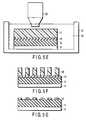
- FIGS. 1A to 1 Gare sectional views each showing procedures in a pattern forming method according to a first embodiment
- FIG. 2is a sectional view schematically showing a pattern release when a pattern has been formed in a conventional three-layer resist process
- FIGS. 3A to 3 Eare sectional views each showing procedures in a pattern forming method in a second embodiment
- FIG. 4is a view schematically showing a resist pattern breakage phenomenon which occurs due to shortage of resist strength
- FIGS. 5A to 5 Gare sectional views each showing procedures in a pattern forming method according to a third embodiment.
- the first embodimentdescribes a pattern forming method in a three-layer resist process.
- an anti-reflection film made of carbonis defined as a lower-layered film
- an SOG filmspin on dielectric film
- a chemically amplified resist filmphotosensitive film
- a pattern forming method for a chemically amplified resist film which is an upper-layered film in the three-layer resist processwill be specifically described.
- FIGS. 1A to 1 Gare sectional views each showing procedures in a pattern forming method according to a first embodiment of the present invention.
- a solution including an anti-reflection materialis coated on a substrate 11 with a spin coating technique. As shown in FIG. 1A , heating is carried out under a condition of 300° C. for 120 seconds, whereby an anti-reflection film 12 of 300 nm in film thickness is formed on the substrate 11 .
- spun-on C made of carbonfor example, is used for the anti-reflection film 12 .
- a spin on dielectric materialis coated on the anti-reflection film 12 with the spin coating technique. As shown in FIG. 1B , heating is carried out under a condition of 350° C. for 120 seconds, whereby an SOG film 13 of 50 nm in film thickness is formed on the anti-reflection film 12 .
- pure water (ultra-pure water) 15is supplied from a nozzle 14 onto the SOG film 13 while the substrate 11 is rotated. A washing process is carried out for 60 seconds. The surface of the SOG film 13 is dried with a spin drying technique.
- the substrate 11is placed on a hot plate 16 .
- the substrate 11is heated under a condition of 200° C. for 60 seconds, whereby a water molecule adsorbed onto the surface of the SOG film 13 is removed. This heating process may be omitted if there is no necessity.
- a coating material for ArF light (193 nm in wavelength) chemically amplified positive resist filmis coated onto the SOG film 13 with the spin coating technique. As shown in FIG. 1E , by heating at 120° C. for 60 seconds, a resist film 17 of 200 nm in film thickness is formed on the SOG film 13 .
- a pattern formed on an exposure reticle by using an ArF excimer laseris reduced, projected, and exposed to the resist film 17 , whereby a latent image is formed on the resist film 17 .
- the substrate 11is heat-treated under a condition of 130° C. for 60 seconds.
- the substrate 11is transported to a developing device. Due to a developing liquid being supplied onto the resist film 17 , a developing process is started. After 30 seconds, in order to stop the developing process and washing, pure water is supplied onto the substrate 11 . After stopping supply of the pure water, the surface of the resist film 17 is dried with a spin drying technique.
- a cross section of the resist pattern formed with the above processeswas observed by using a scanning electronic microscope (SEM).
- SEMscanning electronic microscope
- the SOG film 13is patterned with the line and space pattern 18 being a mask.
- the line and space pattern 18is eliminated while the SOG film 13 is etched.
- the anti-reflection film 12 and the substrate 11are sequentially etched and patterned.
- a chemically amplified resist filmwas formed on the SOG film 13 without carrying out a process of washing the SOG film with pure water, and then, a pattern was reduced, projected, exposed by using the ArF excimer laser, and developed, whereby a 1:1 line and space pattern 21 was formed.
- a cross section of the formed resist patternwas observed by using the scanning electronic microscope (SEM). In a pattern of 100 nm or less in dimensions of the 1:1 line and space pattern 21 , thinning was observed at a lower end of the pattern 21 , and much of the line and space pattern 21 was released on a boundary surface between the pattern 21 and the SOG film 13 ( FIG. 2 ).
- a subsidiary component other than a resinis contained for the purpose of enhancing preservation stability of the spin on dielectric material.
- segregation in which this subsidiary component has been segregatedis formed in the vicinity of the surface of the SOG film.
- the subsidiary component contained in the segregated layerdiffuses into the chemically amplified resist film, and a resist pattern bottom part is decomposed. In this manner, there occurs a resist pattern release on a boundary surface between the chemically amplified resist and the SOG as shown in FIG. 2 .
- the surfaceis washed by pure water, whereby the subsidiary component which is excessively segregated in the SOG film top layer can be eliminated.
- the degree of diffusion of the subsidiary component into the chemically amplified resistcan be restricted, and a resist pattern release on the boundary surface between the chemically amplified resist and the SOG film can be restricted.
- the wash chemicalis not limited to the pure water.
- itis more effective to use ozone water or hydrogen peroxide water. Since these chemicals have oxidization properties, the subsidiary component is oxidized and decomposed, whereby advantageous effect of eliminating the subsidiary component segregated on the SOG top layer is enhanced more significantly.
- ozone waterwas used for wash water, a resist pattern release produced on the boundary surface between the resist and the SOG film was not observed even in a fine 1:1 line and space pattern of 60 nm in dimension.
- a heating processis carried out under a condition of 200° C. for 60 seconds in order to eliminate a water molecule adsorbed to the SOG film top layer.
- the heating process conditionis not limited thereto. A heating temperature and a heating time will suffice if they can eliminate the water molecule adsorbed to the SOG film top layer.
- the subsidiary componentcan be removed by the washing process only in the vicinity of the SOG top layer. Therefore, there is a danger that, if the heating temperature is excessively high, the subsidiary component remaining in the SOG film is segregated again on the SOG film top layer during the heating process.
- the heating process temperature for eliminating the adsorbed waterbe equal to lower than at least the film forming temperature of the SOF film.
- the heating process conditionmay be properly selected according to type of the SOG film to be used. Further, this heating process may be omitted if there is no necessity.
- the present embodimenthas described a case of the SOG film, a material which is effective to the present embodiment is not limited thereto. Specifically, the embodiment is effective to a material classified into the publicly known spin-on dielectric (SOD) film.
- SODspin-on dielectric
- a chemically amplified resist which has reactivity with ArFwas used as a resist for use in the present embodiment, similar advantageous effect was attained for another alicyclic resin (acrylic based, cyclo olefin methyl adamantine (coma) based, and hybrid based resins) as well without being limited thereto.
- the embodimentis also effective to a resin having an aromatic compound.
- advantageous effectwas verified with respect to an i-beam or g-beam resist having a novolac resin; a KrF resist composed of a resin having a polyvinylphenol framework; an electron beam exposure resist; or a soft X-ray (EUV) exposure resist as well.
- EUVsoft X-ray
- a multi-layered film having a three-layer structureis formed on a substrate.
- an anti-reflection film made of carbonis defined as a lower-layered film;
- an SOG filmis defined as an intermediate film;
- a chemically amplified resist filmis defined as an upper-layered film.
- a specific descriptionwill be given with respect to a method for forming a pattern of a chemically amplified resist layer which is an upper-layered film in the three-layer structure.
- FIGS. 3A to 3 Eare sectional views each showing procedures in a pattern forming method according to a second embodiment of the present invention.
- an anti-reflection film 12 and an SOG film 13are formed on a substrate 11 .
- the substrate 11is processed to be heated under a condition of 100° C. for 60 seconds in a processing unit filled with hexamethyl disilazane steam.
- a water molecule adsorbed to the surface of the SOG film 13is removed by heating the substrate under a condition of 200° C. for 60 seconds.
- a line and space pattern 18is formed. Further, with the pattern 18 as a mask, the SOG film 13 and the substrate 11 are etched.
- a hydrophobic processing for the SOG top layeris carried out by exposure to hexamethylene disilazane steam.
- An organic film including an ArF chemically amplified positive resist filmis highly hydrophobic.
- the wash chemicalis not limited to the pure water.
- itis more effective to use ozone water or hydrogen peroxide water. Since these chemicals oxidize and decompose the subsidiary component, and the SOG resin itself is oxidized, a hydroxide group or a carboxylic group is produced on the surface of the SOG film 13 . In this manner, the surface of the SOG film 13 becomes hydrophilic, and there is a danger that some resist resins to be used lowers coherence with the SOG film.
- the hydroxide group or carboxylic group formed on the SOG resin top layercan be eliminated by carrying out the hydrophilic process after terminating the washing process, and the coherence with the SOG film can be maintained.
- the ozone waterwas used for wash water, even in a fine 1:1 line and space pattern of 55 nm in dimension, a resist pattern release produced on a boundary surface between the resist and the SOG film was not observed.
- FIG. 4in a pattern 31 of less than 60 nm, a pattern breakage phenomenon occurred due to breakage of the resist produced by insufficient strength of the resist ( FIG. 4 ).
- the hydrophobic processing for the SOG film top layeris carried out after washing the SOG film surface.
- a heating processis carried out under a condition of 100° C. for 60 seconds in a processing unit filled with hexamethylene disilazane steam.
- the heating process conditionis not limited thereto.
- An optimal processing conditionmay be properly selected such that a resist pattern does not break according to a material for a resist film or an intermediate film to be used.
- other silazanes, chlorosilanes, or alkoxysilanesbe selected for the hydrophobic processing without being limited to hexamethylene disilazane as long as it is properly optimal.
- a heating processis carried out under a condition of 200° C. for 60 seconds in order to remove a water component adsorbed to the SOG film top surface.
- the heating process conditionis not limited thereto.
- an optimal heating process conditionsuch as a temperature and time under which the water molecule adsorbed to the SOG film top layer and which is properly optimal according to the type of SOG film may be selected. Further, this heating process may be omitted if there is no necessity.
- the embodimenthas described a case of the SOG film, a material for which the processing described in the embodiment is efficient is not limited thereto. Specifically, the present embodiment is effective to a material classified into a publicly known SOD film.
- the present embodimentdescribes a pattern forming method when a resist pattern is formed by a liquid impregnation type projecting and exposure apparatus.
- a pattern forming method in a three-layer resist processwill be described.
- An anti-reflection film made of carbonis defined as a lower-layered film
- an SOG filmis defined as an intermediate film
- a chemically amplified resistis defined as an upper-layered film.
- FIGS. 5A to 5 Gare sectional views each showing procedures in a pattern forming method according to a third embodiment of the present embodiment.
- an anti-reflection film 12 and a SOG film 13are sequentially formed on a target substrate 11 .
- ArF light (193 nm in wavelength) chemically amplified positive resist materialis coated on the SOG film 13 in accordance with a spin coating technique, and then, heating is carried out at 120° C. for 60 seconds, thereby forming a chemically amplified positive resist film 17 of 200 nm in film thickness.
- the target substrate 11is placed on a hot plate 16 .
- the substrate 11is heated under a condition of 130° C. for 60 seconds.
- a desired pattern provided on a reticleis transferred to the positive resist film 17 by using an ArF excimer laser, and a latent image is formed on the positive resist film 17 .
- the substrate 11is placed in a liquid tank 31 , and a pattern is projected, and exposed on the positive resist film 17 via a water layer 33 formed in an optical path between the chemically amplified positive resist film 17 and an optical system 32 of the projecting and exposure apparatus.
- the substrate 11is heat-treated under a condition of 130° C. for 60 seconds.
- the substrate 11is transported to a developing device.
- the developing liquidis supplied onto the resist film 17 , whereby a developing process is started.
- pure wateris supplied onto the rotating target substrate 11 .
- the surface of the resist film 17is dried in accordance with the spin drying technique.
- the SOG film 13is patterned.
- the pattern 18is eliminated.
- the anti-reflection film 12 and the target substrate 11are sequentially etched and patterned.
- the uniformity of the dimensions in the substrate surface of the formed pattern 18was 3 nm in 3 ⁇ .
- 3 ⁇was 1.5 nm in a conventional method.
- the uniformity of the dimensions in the target substrate surface of the resist patternwas 7 nm in 3 ⁇ .
- the dispersion in line edge roughness of the resist patternwas 4 nm in 3 ⁇ .
- a semiconductor device fabricated by processing for a mask a resist pattern produced by using the method described in the present embodimentwas more successfully improved in yield than a semiconductor device fabricated without carrying out this processing, and device reliability was successfully enhanced.
- Some chemically amplified positive resist materialcontains an optical acid generating material or the like which is decomposed when light is emitted and which generates a strong acid, in addition to a resin which becomes a film framework. If a heating process is carried out after exposure, a resist resin is decomposed by an action of the acid produced from an optical acid generating material, whereby a light emitting portion becomes soluble to a developing liquid. As a result, a resist pattern is formed.
- the optical acid generating materialis segregated on the surface of the chemically amplified resist film when the chemically amplified resist film is coated to form an film on the substrate. However, during immersion exposure, the optical acid generating material is dissolved in the liquid contained in the liquid tank provided between the substrate and a projecting optical system.
- the optical acid generating material dissolved according to the liquid liquidationalso liquidates, and the optical acid generating material is localized on the chemically amplified resist film surface.
- the resist resin of the light emitting portionis dissolved according to the amount of the optical acid generating material localized on the surface of the substrate, and a resist pattern is formed.
- the dimensional uniformity in the substrate surface of the chemically amplified resist patterndeteriorates.
- the washing processis carried out with pure water after forming the chemically amplified resist film, the optical acid generating material excessively segregated in the top layer of the chemically amplified resist film can be removed.
- the dimensional uniformity or line edge roughness in the surface of the substrate of the chemically amplified resist patterncan be improved as compared with the conventional method.
- the present embodimenthas described a case in which the chemically amplified resist surface was washed before immersion exposure by using the immersion type projecting and exposure apparatus.
- the effectiveness of the present inventionis not limited to washing the surface of the chemically amplified resist.
- the liquid impregnation exposure processincludes a process for forming a protective film in a resist film in order to prevent water penetration into the chemically amplified resist or pattern deterioration due to dissolution of the substance included in the resist film into water.
- a protective filmcannot eliminate effect of water perfectly.
- the surface of the protection film formed on the chemically amplified resistis washed before immersion or exposure, whereby the dimensional uniformity or line edge roughness in the surface of the substrate can be improved as compared with a case in which no washing process has been carried out.
- the embodimenthas described a pattern forming method when a resist pattern is formed by using a immersion type projecting and exposure apparatus.
- the effectiveness of the present inventionis not limited to a case of using the immersion type exposure apparatus. Even in the case where a resist pattern is formed by using a general exposure apparatus and in the case where a desired pattern is reduced, projected, and exposed after carrying out the washing process after forming the chemically amplified resist film, the dimensional uniformity or line edge roughness in the surface of the substrate can be improved as compared with a case in which no washing process has been carried out.
- pure waterwas used as a washing chemical for the chemically amplified resist film
- the washing chemicalis not limited thereto.
- the present inventionis more effective in the case where ozone water or hydrogen peroxide water was used. Since these chemicals have oxidization properties, the subsidiary component is oxidized and decomposed, whereby advantageous effect of eliminating the subsidiary component segregated on the top layer of the chemically amplified resist is enhanced more significantly. The dimensional uniformity or line edge roughness in the surface of the target substrate is improved more significantly.
- a heating processis carried out under a condition of 130° C. for 60 seconds.
- the heating process conditionis not limited thereto. Any heating temperature or heating time may be used as long as it can remove the water molecule adsorbed to the top layer of the chemically amplified resist film.
- a material for which the present invention is effectiveis not limited thereto. Specifically, the invention is effective to a material classified into a publicly known SOD film.
- the chemically amplified resist having reactivity with ArF lightwas used as a resist for use in the present embodiment, a similar advantageous effect was attained for another alicyclic resin (acryl based, coma based, or hybrid based resin) without being limited thereto.
- the present inventionis also effective to a resin having an aromatic compound. Further, the advantageous effect was verified with respect to an i-beam or g-beam resist having a novolac resin; a KrF resist composed of a resin having a polyvinylphenol framework; an electron beam exposure resist; or a soft X-ray (EUV) exposure resist as well.
- EUVsoft X-ray
Landscapes
- Physics & Mathematics (AREA)
- General Physics & Mathematics (AREA)
- Engineering & Computer Science (AREA)
- Microelectronics & Electronic Packaging (AREA)
- Manufacturing & Machinery (AREA)
- Computer Hardware Design (AREA)
- Condensed Matter Physics & Semiconductors (AREA)
- Power Engineering (AREA)
- Architecture (AREA)
- Structural Engineering (AREA)
- Spectroscopy & Molecular Physics (AREA)
- Photosensitive Polymer And Photoresist Processing (AREA)
- Materials For Photolithography (AREA)
- Exposure Of Semiconductors, Excluding Electron Or Ion Beam Exposure (AREA)
Abstract
Description
- This application is based upon and claims the benefit of priority from prior Japanese Patent Application No. 2004-008290, filed Jan. 15, 2004, the entire contents of which are incorporated herein by reference.
- 1. Field of the Invention
- The present invention relates to a pattern forming method for use in processing a substrate such as a semiconductor substrate, a glass substrate, and a resin substrate.
- 2. Description of the Related Art
- In recent years, there has been a growing demand for highly integrated LSIs. Concurrently, there has been a demand for a processing technique with very high precision for forming a fine device pattern of 100 nm or less in a semiconductor lithography technique. Therefore, in a pattern exposure apparatus, high resolution is accelerated by producing short wavelengths with an excimer laser for use in KrF→ArF→F2. On the other hand, with more fining, pattern breakage of a resist film cannot be ignored. Therefore, a multilayer resist process for preventing pattern breakage by reducing the film thickness of a chemically amplified resist is used.
- For example, as described in Jpn. Pat. Appln. KOKAI Publication No. 6-84787, there has been a problem that an upper-layered resist pattern falls (is released) in a multilayer resist process. In Jpn. Pat. Appln. KOKAI Publication No. 6-84787, it has been reported that an SOG film surface is temporarily subjected to hydrophobic processing, and then, a chemically amplified resist is formed, thereby restricting release of the resist pattern. However, this method has proved insufficient, although a certain advantageous effect is attained in restricting the release of the resist pattern.
- As described above, in the multilayer resist process, there has been a problem that an upper-layered resist pattern is released/falls.
- According to an aspect of the present invention, there is provided a pattern forming method comprising: forming a spin on dielectric film on a substrate; washing the spin on dielectric film by using a washing liquid; drying a surface of the spin on dielectric film after the washing; forming a photosensitive film on the dried spin on dielectric film; emitting energy rays to a predetermined position of the photosensitive film in order to form a latent image on the photosensitive film; developing the photosensitive film in order to form a photosensitive film pattern which corresponds to the latent image; and processing the coating type insulation film with the photosensitive film pattern serving as a mask.
- According to another aspect of the present invention, there is provided a pattern forming method comprising: preparing a first substrate; forming a photosensitive film on the first substrate; washing the photosensitive film by using a first washing liquid; emitting energy rays to a predetermined position of the photosensitive film by using an immersion type exposure in order to form a latent image on the photosensitive film after washing the photosensitive film; developing the photosensitive film in order to form a photosensitive film pattern which corresponds to the latent image; and processing the first substrate with the photosensitive film pattern serving as a mask.
FIGS. 1A to1G are sectional views each showing procedures in a pattern forming method according to a first embodiment;FIG. 2 is a sectional view schematically showing a pattern release when a pattern has been formed in a conventional three-layer resist process;FIGS. 3A to3E are sectional views each showing procedures in a pattern forming method in a second embodiment;FIG. 4 is a view schematically showing a resist pattern breakage phenomenon which occurs due to shortage of resist strength; andFIGS. 5A to5G are sectional views each showing procedures in a pattern forming method according to a third embodiment.- Hereinafter, embodiments of the present invention will be described with reference to the accompanying drawings.
- The first embodiment describes a pattern forming method in a three-layer resist process. In this three-layered film, an anti-reflection film made of carbon is defined as a lower-layered film; an SOG film (spin on dielectric film) is defined as an intermediate film; or a chemically amplified resist film (photosensitive film) is defined as an upper-layered film. Hereinafter, a pattern forming method for a chemically amplified resist film which is an upper-layered film in the three-layer resist process will be specifically described.
FIGS. 1A to1G are sectional views each showing procedures in a pattern forming method according to a first embodiment of the present invention.- First, a solution including an anti-reflection material is coated on a
substrate 11 with a spin coating technique. As shown inFIG. 1A , heating is carried out under a condition of 300° C. for 120 seconds, whereby ananti-reflection film 12 of 300 nm in film thickness is formed on thesubstrate 11. In addition, spun-on C made of carbon, for example, is used for theanti-reflection film 12. - Next, in order to form an intermediate film, a spin on dielectric material is coated on the
anti-reflection film 12 with the spin coating technique. As shown inFIG. 1B , heating is carried out under a condition of 350° C. for 120 seconds, whereby anSOG film 13 of 50 nm in film thickness is formed on theanti-reflection film 12. - Next, as shown in
FIG. 1C , in order to wash a surface of theSOG film 13, pure water (ultra-pure water)15 is supplied from anozzle 14 onto theSOG film 13 while thesubstrate 11 is rotated. A washing process is carried out for 60 seconds. The surface of theSOG film 13 is dried with a spin drying technique. - Next, as shown in
FIG. 1D , thesubstrate 11 is placed on ahot plate 16. Thesubstrate 11 is heated under a condition of 200° C. for 60 seconds, whereby a water molecule adsorbed onto the surface of theSOG film 13 is removed. This heating process may be omitted if there is no necessity. - Next, a coating material for ArF light (193 nm in wavelength) chemically amplified positive resist film is coated onto the
SOG film 13 with the spin coating technique. As shown inFIG. 1E , by heating at 120° C. for 60 seconds, aresist film 17 of 200 nm in film thickness is formed on theSOG film 13. - Next, a pattern formed on an exposure reticle by using an ArF excimer laser is reduced, projected, and exposed to the
resist film 17, whereby a latent image is formed on theresist film 17. Thesubstrate 11 is heat-treated under a condition of 130° C. for 60 seconds. Thesubstrate 11 is transported to a developing device. Due to a developing liquid being supplied onto theresist film 17, a developing process is started. After 30 seconds, in order to stop the developing process and washing, pure water is supplied onto thesubstrate 11. After stopping supply of the pure water, the surface of the resistfilm 17 is dried with a spin drying technique. By carrying out these processes, as shown inFIG. 1F , a 1:1 line andspace pattern 18 is formed on thesubstrate 11. - A cross section of the resist pattern formed with the above processes was observed by using a scanning electronic microscope (SEM). In a pattern of 70 nm in dimensions of the 1:1 line and
space pattern 18 as well, a resist pattern fall/release was not observed on a boundary surface between the resistfilm 17 and theSOG film 13, and it was verified that a vertical pattern was formed. - Next, as shown in
FIG. 1G , theSOG film 13 is patterned with the line andspace pattern 18 being a mask. In general, the line andspace pattern 18 is eliminated while theSOG film 13 is etched. Then, with the SOG film as a mask, theanti-reflection film 12 and thesubstrate 11 are sequentially etched and patterned. - On the other hand, as carried out in a conventional three-layer resist process, a chemically amplified resist film was formed on the
SOG film 13 without carrying out a process of washing the SOG film with pure water, and then, a pattern was reduced, projected, exposed by using the ArF excimer laser, and developed, whereby a 1:1 line andspace pattern 21 was formed. A cross section of the formed resist pattern was observed by using the scanning electronic microscope (SEM). In a pattern of 100 nm or less in dimensions of the 1:1 line andspace pattern 21, thinning was observed at a lower end of thepattern 21, and much of the line andspace pattern 21 was released on a boundary surface between thepattern 21 and the SOG film13 (FIG. 2 ). - As has been described above, a semiconductor device fabricated by processing for a mask the
pattern 18 produced by using the method described in the first embodiment successfully processed a pattern which is finer than a semiconductor device fabricated without carrying out this process, and yield was successfully improved. - In a spin on dielectric material, in addition to a resin serving as a film framework, a subsidiary component other than a resin is contained for the purpose of enhancing preservation stability of the spin on dielectric material. When the spin on dielectric material is coated and sintered to form a film on the substrate, segregation in which this subsidiary component has been segregated is formed in the vicinity of the surface of the SOG film. Next, after a chemically amplified resist film has been formed on this segregated layer, when a desired pattern is reduced, projected, exposed, and developed, the subsidiary component contained in the segregated layer diffuses into the chemically amplified resist film, and a resist pattern bottom part is decomposed. In this manner, there occurs a resist pattern release on a boundary surface between the chemically amplified resist and the SOG as shown in
FIG. 2 . - Therefore, as in the present embodiment, after forming the SOG film, the surface is washed by pure water, whereby the subsidiary component which is excessively segregated in the SOG film top layer can be eliminated. In this manner, the degree of diffusion of the subsidiary component into the chemically amplified resist can be restricted, and a resist pattern release on the boundary surface between the chemically amplified resist and the SOG film can be restricted.
- Further, in the present embodiment, although pure water was used as a wash chemical for the SOG film, the wash chemical is not limited to the pure water. In particular, it is more effective to use ozone water or hydrogen peroxide water. Since these chemicals have oxidization properties, the subsidiary component is oxidized and decomposed, whereby advantageous effect of eliminating the subsidiary component segregated on the SOG top layer is enhanced more significantly. In the case where the ozone water was used for wash water, a resist pattern release produced on the boundary surface between the resist and the SOG film was not observed even in a fine 1:1 line and space pattern of 60 nm in dimension.
- Furthermore, in the present embodiment, after terminating the process of washing the SOG film, a heating process is carried out under a condition of 200° C. for 60 seconds in order to eliminate a water molecule adsorbed to the SOG film top layer. However, the heating process condition is not limited thereto. A heating temperature and a heating time will suffice if they can eliminate the water molecule adsorbed to the SOG film top layer. However, the subsidiary component can be removed by the washing process only in the vicinity of the SOG top layer. Therefore, there is a danger that, if the heating temperature is excessively high, the subsidiary component remaining in the SOG film is segregated again on the SOG film top layer during the heating process. Accordingly, it is desirable that the heating process temperature for eliminating the adsorbed water be equal to lower than at least the film forming temperature of the SOF film. In addition, the heating process condition may be properly selected according to type of the SOG film to be used. Further, this heating process may be omitted if there is no necessity.
- Although the present embodiment has described a case of the SOG film, a material which is effective to the present embodiment is not limited thereto. Specifically, the embodiment is effective to a material classified into the publicly known spin-on dielectric (SOD) film.
- Moreover, although a chemically amplified resist which has reactivity with ArF was used as a resist for use in the present embodiment, similar advantageous effect was attained for another alicyclic resin (acrylic based, cyclo olefin methyl adamantine (coma) based, and hybrid based resins) as well without being limited thereto. In addition, the embodiment is also effective to a resin having an aromatic compound. Further, advantageous effect was verified with respect to an i-beam or g-beam resist having a novolac resin; a KrF resist composed of a resin having a polyvinylphenol framework; an electron beam exposure resist; or a soft X-ray (EUV) exposure resist as well.
- In the second embodiment, as in the first embodiment, a description will be given with respect to a pattern forming method for forming a resist pattern even in a state in which a segregated layer has formed on an SOG film top layer. A multi-layered film having a three-layer structure is formed on a substrate. In this multi-layered film, an anti-reflection film made of carbon is defined as a lower-layered film; an SOG film is defined as an intermediate film; and a chemically amplified resist film is defined as an upper-layered film. Hereinafter, a specific description will be given with respect to a method for forming a pattern of a chemically amplified resist layer which is an upper-layered film in the three-layer structure.
FIGS. 3A to3E are sectional views each showing procedures in a pattern forming method according to a second embodiment of the present invention.- First, as shown in
FIG. 3A , as in the first embodiment, ananti-reflection film 12 and anSOG film 13 are formed on asubstrate 11. - Next, as shown in
FIG. 3B , in order to carry out a washing process of a surface of theSOG film 13,pure water 15 is supplied onto theSOG film 13 while thesubstrate 11 is rotated. The washing process is carried out for 60 seconds. After the washing process, theSOG film 13 is dried with a spin drying technique. - Next, as shown in
FIG. 3C , in order to carry out hydrophobic processing of the surface of theSOG film 13, thesubstrate 11 is processed to be heated under a condition of 100° C. for 60 seconds in a processing unit filled with hexamethyl disilazane steam. - Next, as shown in
FIG. 3D , a water molecule adsorbed to the surface of theSOG film 13 is removed by heating the substrate under a condition of 200° C. for 60 seconds. Through a process similar to that of the first embodiment, as shown inFIG. 3E , a line andspace pattern 18 is formed. Further, with thepattern 18 as a mask, theSOG film 13 and thesubstrate 11 are etched. - When a cross section of the
pattern 18 formed with the above processes was observed by using a scanning electronic microscope (SEM), even if dimensions of the 1:1 line andspace pattern 18 was 60 nm, a resist pattern release was not observed on a boundary surface between the resist film and the SOG film, and avertical pattern 18 was formed. - As has been described above, a semiconductor device fabricated by processing for a mask the resist pattern produced by using the method described in the second embodiment successfully processed a pattern which is finer than a semiconductor device fabricated without carrying out this process, and yield was successfully improved.
- In the present embodiment, after terminating the process of washing the SOG film, a hydrophobic processing for the SOG top layer is carried out by exposure to hexamethylene disilazane steam. An organic film including an ArF chemically amplified positive resist film is highly hydrophobic. By performing the hydrophobic processing for the SOG film after the subsidiary component has been removed in accordance with the washing process, when a next chemically amplified resist film is formed on the SOG film, coherence between the chemically amplified resist film and the SOG film is improved. Thus, the advantageous effect that a resist pattern release can be restricted more significantly. Moreover, with the present embodiment, hydrophobic process is performed after the washing and heating process is carried out after that. However, a processing order is not limited to this. For example, it is also possible to use as the order of washing processing, heating processing, and hydrophobic processing.
- In addition, in the present embodiment, although pure water was used as a wash chemical for the SOG film, the wash chemical is not limited to the pure water. In particular, it is more effective to use ozone water or hydrogen peroxide water. Since these chemicals oxidize and decompose the subsidiary component, and the SOG resin itself is oxidized, a hydroxide group or a carboxylic group is produced on the surface of the
SOG film 13. In this manner, the surface of theSOG film 13 becomes hydrophilic, and there is a danger that some resist resins to be used lowers coherence with the SOG film. Therefore, the hydroxide group or carboxylic group formed on the SOG resin top layer can be eliminated by carrying out the hydrophilic process after terminating the washing process, and the coherence with the SOG film can be maintained. For example, in the case where the ozone water was used for wash water, even in a fine 1:1 line and space pattern of 55 nm in dimension, a resist pattern release produced on a boundary surface between the resist and the SOG film was not observed. However, as shown inFIG. 4 , in apattern 31 of less than 60 nm, a pattern breakage phenomenon occurred due to breakage of the resist produced by insufficient strength of the resist (FIG. 4 ). - In the present embodiment, the hydrophobic processing for the SOG film top layer is carried out after washing the SOG film surface. Thus, a heating process is carried out under a condition of 100° C. for 60 seconds in a processing unit filled with hexamethylene disilazane steam. However, the heating process condition is not limited thereto. An optimal processing condition may be properly selected such that a resist pattern does not break according to a material for a resist film or an intermediate film to be used. In addition, other silazanes, chlorosilanes, or alkoxysilanes be selected for the hydrophobic processing without being limited to hexamethylene disilazane as long as it is properly optimal.
- In the present embodiment, after the hydrophobic processing for the SOG film, a heating process is carried out under a condition of 200° C. for 60 seconds in order to remove a water component adsorbed to the SOG film top surface. However, the heating process condition is not limited thereto. As in the first embodiment, an optimal heating process condition such as a temperature and time under which the water molecule adsorbed to the SOG film top layer and which is properly optimal according to the type of SOG film may be selected. Further, this heating process may be omitted if there is no necessity.
- Although the embodiment has described a case of the SOG film, a material for which the processing described in the embodiment is efficient is not limited thereto. Specifically, the present embodiment is effective to a material classified into a publicly known SOD film.
- In addition, although a chemically amplified resist which has reactivity with ArF was used as a resist for use in the present embodiment, similar advantageous effect was attained for another alicyclic resin (acryl based, coma based, or hybrid based resin). Further, advantageous effect was verified with respect to an i-beam or g-beam resist having a novolac resin; a KrF resist composed of a resin having a polyvinylphenol framework; an electron beam exposure resist; or a soft X-ray (EUV) exposure resist as well.
- The present embodiment describes a pattern forming method when a resist pattern is formed by a liquid impregnation type projecting and exposure apparatus. Here, as is the above-described embodiments, a pattern forming method in a three-layer resist process will be described. An anti-reflection film made of carbon is defined as a lower-layered film, an SOG film is defined as an intermediate film, and a chemically amplified resist is defined as an upper-layered film.
- In the first and second embodiments, after washing the SOG film surface, a resist film was formed. As in washing the SOG film, when a resist film surface before developing the resist film was washed, an advantageous effect was attained for improvement of dimensional uniformity of a pattern after developed or for restriction of line edge roughness. An embodiment of washing the surface of the resist film will be described below.
FIGS. 5A to5G are sectional views each showing procedures in a pattern forming method according to a third embodiment of the present embodiment.- As shown in
FIG. 5A , as in the first embodiment or the second embodiment, ananti-reflection film 12 and aSOG film 13 are sequentially formed on atarget substrate 11. - Then, as shown in
FIG. 5B , ArF light (193 nm in wavelength) chemically amplified positive resist material is coated on theSOG film 13 in accordance with a spin coating technique, and then, heating is carried out at 120° C. for 60 seconds, thereby forming a chemically amplified positive resistfilm 17 of 200 nm in film thickness. - Next, as shown in
FIG. 5C , in order to wash the surface of the chemically amplified positive resistfilm 17,pure water 15 is supplied onto the chemically amplified positive resistfilm 17 while thetarget substrate 11 is rotated. The washing process is carried out for 60 seconds. After the washing process, the surface of the chemically amplified positive resistfilm 17 is dried in accordance with a spin drying technique. - Subsequently, as shown in
FIG. 5D , thetarget substrate 11 is placed on ahot plate 16. In order to remove a water molecule adsorbed to the surface of the chemically amplified positive resistfilm 17, thesubstrate 11 is heated under a condition of 130° C. for 60 seconds. - Next, in a liquid impregnation type projecting and exposure apparatus described in Jpn. Pat. Appln. KOKAI Publication No. 6-124873, a desired pattern provided on a reticle is transferred to the positive resist
film 17 by using an ArF excimer laser, and a latent image is formed on the positive resistfilm 17. For example, as shown inFIG. 5E , thesubstrate 11 is placed in aliquid tank 31, and a pattern is projected, and exposed on the positive resistfilm 17 via awater layer 33 formed in an optical path between the chemically amplified positive resistfilm 17 and anoptical system 32 of the projecting and exposure apparatus. - The
substrate 11 is heat-treated under a condition of 130° C. for 60 seconds. Thesubstrate 11 is transported to a developing device. The developing liquid is supplied onto the resistfilm 17, whereby a developing process is started. After 30 seconds, in order to stop the developing process and washing, pure water is supplied onto therotating target substrate 11. After stopping supply of the pure water, the surface of the resistfilm 17 is dried in accordance with the spin drying technique. By carrying out this processing, as shown inFIG. 5F , a 1:1 line andspace pattern 18 of 90 nm in thickness is formed on thesubstrate 11. - Subsequently, as shown in
FIG. 5G , with thepattern 18 of the resist film being a mask, theSOG film 13 is patterned. In general, while theSOG film 13 is etched, thepattern 18 is eliminated. Then, with theSOG film 13 being a mask, theanti-reflection film 12 and thetarget substrate 11 are sequentially etched and patterned. - In accordance with the above process, the uniformity of the dimensions in the substrate surface of the formed
pattern 18 was 3 nm in 3σ. In addition, when dispersion in line edge roughness of thepattern 18 was measured, 3σ was 1.5 nm in a conventional method. On the other hand, as is carried out in a three-layer resist process using a conventional immersion exposure apparatus, when a 1:1 line and space pattern of 90 nm was formed by reducing, projecting, exposing, and developing a pattern without carrying out the washing process for the chemically amplified positive resist film with pure water, the uniformity of the dimensions in the target substrate surface of the resist pattern was 7 nm in 3σ. Further, the dispersion in line edge roughness of the resist pattern was 4 nm in 3σ. - As has been described above, a semiconductor device fabricated by processing for a mask a resist pattern produced by using the method described in the present embodiment was more successfully improved in yield than a semiconductor device fabricated without carrying out this processing, and device reliability was successfully enhanced.
- Some chemically amplified positive resist material contains an optical acid generating material or the like which is decomposed when light is emitted and which generates a strong acid, in addition to a resin which becomes a film framework. If a heating process is carried out after exposure, a resist resin is decomposed by an action of the acid produced from an optical acid generating material, whereby a light emitting portion becomes soluble to a developing liquid. As a result, a resist pattern is formed. The optical acid generating material is segregated on the surface of the chemically amplified resist film when the chemically amplified resist film is coated to form an film on the substrate. However, during immersion exposure, the optical acid generating material is dissolved in the liquid contained in the liquid tank provided between the substrate and a projecting optical system. As in a general exposure apparatus, when exposure was carried out by a step and repeat operation, liquidation occurs with the liquid. Thus, the optical acid generating material dissolved according to the liquid liquidation also liquidates, and the optical acid generating material is localized on the chemically amplified resist film surface. Next, when the heating process and developing process are carried out while the optical acid generating material is localized on the surface of the substrate, the resist resin of the light emitting portion is dissolved according to the amount of the optical acid generating material localized on the surface of the substrate, and a resist pattern is formed. Thus, the dimensional uniformity in the substrate surface of the chemically amplified resist pattern deteriorates.
- Therefore, as in the embodiment, the washing process is carried out with pure water after forming the chemically amplified resist film, the optical acid generating material excessively segregated in the top layer of the chemically amplified resist film can be removed. In this manner, the dimensional uniformity or line edge roughness in the surface of the substrate of the chemically amplified resist pattern can be improved as compared with the conventional method.
- The present embodiment has described a case in which the chemically amplified resist surface was washed before immersion exposure by using the immersion type projecting and exposure apparatus. However, the effectiveness of the present invention is not limited to washing the surface of the chemically amplified resist. The liquid impregnation exposure process includes a process for forming a protective film in a resist film in order to prevent water penetration into the chemically amplified resist or pattern deterioration due to dissolution of the substance included in the resist film into water. However, even such a protective film cannot eliminate effect of water perfectly. Therefore, as in the present invention, the surface of the protection film formed on the chemically amplified resist is washed before immersion or exposure, whereby the dimensional uniformity or line edge roughness in the surface of the substrate can be improved as compared with a case in which no washing process has been carried out.
- The embodiment has described a pattern forming method when a resist pattern is formed by using a immersion type projecting and exposure apparatus. However, the effectiveness of the present invention is not limited to a case of using the immersion type exposure apparatus. Even in the case where a resist pattern is formed by using a general exposure apparatus and in the case where a desired pattern is reduced, projected, and exposed after carrying out the washing process after forming the chemically amplified resist film, the dimensional uniformity or line edge roughness in the surface of the substrate can be improved as compared with a case in which no washing process has been carried out.
- Further, in the embodiment, pure water was used as a washing chemical for the chemically amplified resist film, the washing chemical is not limited thereto. In particular, the present invention is more effective in the case where ozone water or hydrogen peroxide water was used. Since these chemicals have oxidization properties, the subsidiary component is oxidized and decomposed, whereby advantageous effect of eliminating the subsidiary component segregated on the top layer of the chemically amplified resist is enhanced more significantly. The dimensional uniformity or line edge roughness in the surface of the target substrate is improved more significantly.
- Furthermore, in the embodiment, after terminating the process of washing the chemically amplified resist film, in order to remove the water molecule adsorbed to the top layer of the chemically amplified resist film, a heating process is carried out under a condition of 130° C. for 60 seconds. However, the heating process condition is not limited thereto. Any heating temperature or heating time may be used as long as it can remove the water molecule adsorbed to the top layer of the chemically amplified resist film.
- Although the present embodiment has described a case of the SOG film, a material for which the present invention is effective is not limited thereto. Specifically, the invention is effective to a material classified into a publicly known SOD film.
- Moreover, although the chemically amplified resist having reactivity with ArF light was used as a resist for use in the present embodiment, a similar advantageous effect was attained for another alicyclic resin (acryl based, coma based, or hybrid based resin) without being limited thereto. In addition, the present invention is also effective to a resin having an aromatic compound. Further, the advantageous effect was verified with respect to an i-beam or g-beam resist having a novolac resin; a KrF resist composed of a resin having a polyvinylphenol framework; an electron beam exposure resist; or a soft X-ray (EUV) exposure resist as well.
- Additional advantages and modifications will readily occur to those skilled in the art. Therefore, the invention in its broader aspects is not limited to the specific details and representative embodiments shown and described herein. Accordingly, various modifications may be made without departing from the spirit or scope of the general inventive concept as defined by the appended claims and their equivalents.
Claims (20)
Priority Applications (4)
| Application Number | Priority Date | Filing Date | Title |
|---|---|---|---|
| US12/926,134US8728943B2 (en) | 2004-01-15 | 2010-10-27 | Pattern forming method and manufacturing method of semiconductor device |
| US14/258,611US9202722B2 (en) | 2004-01-15 | 2014-04-22 | Pattern forming method and manufacturing method of semiconductor device |
| US14/919,919US9601331B2 (en) | 2004-01-15 | 2015-10-22 | Pattern forming method and manufacturing method of semiconductor device |
| US15/456,641US9897918B2 (en) | 2004-01-15 | 2017-03-13 | Pattern forming method and manufacturing method of semiconductor device |
Applications Claiming Priority (2)
| Application Number | Priority Date | Filing Date | Title |
|---|---|---|---|
| JP2004008290AJP3857692B2 (en) | 2004-01-15 | 2004-01-15 | Pattern formation method |
| JP2004-008290 | 2004-01-15 |
Related Child Applications (1)
| Application Number | Title | Priority Date | Filing Date |
|---|---|---|---|
| US12/926,134ContinuationUS8728943B2 (en) | 2004-01-15 | 2010-10-27 | Pattern forming method and manufacturing method of semiconductor device |
Publications (2)
| Publication Number | Publication Date |
|---|---|
| US20050176254A1true US20050176254A1 (en) | 2005-08-11 |
| US7851363B2 US7851363B2 (en) | 2010-12-14 |
Family
ID=34821693
Family Applications (5)
| Application Number | Title | Priority Date | Filing Date |
|---|---|---|---|
| US11/034,975Expired - LifetimeUS7851363B2 (en) | 2004-01-15 | 2005-01-14 | Pattern forming method and manufacturing method of semiconductor device |
| US12/926,134Active2025-12-26US8728943B2 (en) | 2004-01-15 | 2010-10-27 | Pattern forming method and manufacturing method of semiconductor device |
| US14/258,611Expired - LifetimeUS9202722B2 (en) | 2004-01-15 | 2014-04-22 | Pattern forming method and manufacturing method of semiconductor device |
| US14/919,919Expired - Fee RelatedUS9601331B2 (en) | 2004-01-15 | 2015-10-22 | Pattern forming method and manufacturing method of semiconductor device |
| US15/456,641Expired - LifetimeUS9897918B2 (en) | 2004-01-15 | 2017-03-13 | Pattern forming method and manufacturing method of semiconductor device |
Family Applications After (4)
| Application Number | Title | Priority Date | Filing Date |
|---|---|---|---|
| US12/926,134Active2025-12-26US8728943B2 (en) | 2004-01-15 | 2010-10-27 | Pattern forming method and manufacturing method of semiconductor device |
| US14/258,611Expired - LifetimeUS9202722B2 (en) | 2004-01-15 | 2014-04-22 | Pattern forming method and manufacturing method of semiconductor device |
| US14/919,919Expired - Fee RelatedUS9601331B2 (en) | 2004-01-15 | 2015-10-22 | Pattern forming method and manufacturing method of semiconductor device |
| US15/456,641Expired - LifetimeUS9897918B2 (en) | 2004-01-15 | 2017-03-13 | Pattern forming method and manufacturing method of semiconductor device |
Country Status (2)
| Country | Link |
|---|---|
| US (5) | US7851363B2 (en) |
| JP (1) | JP3857692B2 (en) |
Cited By (12)
| Publication number | Priority date | Publication date | Assignee | Title |
|---|---|---|---|---|
| US20060152693A1 (en)* | 2004-12-06 | 2006-07-13 | Dainippon Screen Mfg. Co., Ltd. | Substrate processing apparatus |
| US20070071439A1 (en)* | 2005-09-28 | 2007-03-29 | Koji Kaneyama | Substrate processing apparatus |
| US20090035705A1 (en)* | 2007-07-30 | 2009-02-05 | Shinichi Ito | Method of forming pattern, method of manufacturing semiconductor device, and cleaning apparatus |
| US20100129526A1 (en)* | 2004-12-06 | 2010-05-27 | Sokudo Co., Ltd. | Substrate processing apparatus |
| US20100136492A1 (en)* | 2004-12-06 | 2010-06-03 | Sokudo Co., Ltd. | Substrate processing apparatus and substrate processing method |
| US20100143849A1 (en)* | 2008-12-05 | 2010-06-10 | Tatsuhiko Ema | Semiconductor device manufacturing method |
| US20100190116A1 (en)* | 2004-11-10 | 2010-07-29 | Sokudo Co., Ltd. | Substrate processing apparatus and substrate processing method |
| US20100267233A1 (en)* | 2009-04-17 | 2010-10-21 | Tatsuhiko Koide | Method of manufacturing semiconductor device |
| US20110139192A1 (en)* | 2009-12-15 | 2011-06-16 | Tatsuhiko Koide | Surface treatment apparatus and method for semiconductor substrate |
| US9703199B2 (en) | 2004-12-06 | 2017-07-11 | Screen Semiconductor Solutions Co., Ltd. | Substrate processing apparatus |
| US10048593B2 (en) | 2004-03-24 | 2018-08-14 | Toshiba Memory Corporation | Resist pattern forming method, semiconductor apparatus using said method, and exposure apparatus thereof |
| US11029597B2 (en) | 2016-02-29 | 2021-06-08 | Fujifilm Corporation | Method for producing pattern laminate, method for producing reversal pattern, and pattern laminate |
Families Citing this family (13)
| Publication number | Priority date | Publication date | Assignee | Title |
|---|---|---|---|---|
| JP3857692B2 (en)* | 2004-01-15 | 2006-12-13 | 株式会社東芝 | Pattern formation method |
| JP2008028037A (en) | 2006-07-19 | 2008-02-07 | Nec Electronics Corp | Manufacturing method of semiconductor device |
| US7838425B2 (en) | 2008-06-16 | 2010-11-23 | Kabushiki Kaisha Toshiba | Method of treating surface of semiconductor substrate |
| JP5516931B2 (en)* | 2009-03-12 | 2014-06-11 | ルネサスエレクトロニクス株式会社 | Resist pattern forming method |
| JP5404361B2 (en) | 2009-12-11 | 2014-01-29 | 株式会社東芝 | Semiconductor substrate surface treatment apparatus and method |
| JP2011146535A (en)* | 2010-01-14 | 2011-07-28 | Renesas Electronics Corp | Pattern forming method for multilayer resist, method of manufacturing semiconductor device, and semiconductor device |
| JP2012084789A (en) | 2010-10-14 | 2012-04-26 | Toshiba Corp | Method for manufacturing semiconductor device and semiconductor manufacturing equipment |
| US9018089B2 (en)* | 2011-08-30 | 2015-04-28 | International Business Machines Corporation | Multiple step anneal method and semiconductor formed by multiple step anneal |
| JP5813604B2 (en)* | 2012-09-21 | 2015-11-17 | 株式会社東芝 | Pattern formation method |
| KR101649553B1 (en)* | 2014-11-07 | 2016-08-22 | 서울시립대학교 산학협력단 | Organic field-effect transistors, and method for preparing thereof |
| JP6236481B2 (en)* | 2016-02-17 | 2017-11-22 | 東京エレクトロン株式会社 | Pattern formation method |
| CN114424321A (en)* | 2019-09-25 | 2022-04-29 | 东京毅力科创株式会社 | patterned substrate |
| CN114114842B (en)* | 2021-11-25 | 2025-07-01 | 杭州福斯特电子材料有限公司 | A dry film resist laminate, resin composition and preparation method thereof |
Citations (11)
| Publication number | Priority date | Publication date | Assignee | Title |
|---|---|---|---|---|
| US5667922A (en)* | 1996-04-26 | 1997-09-16 | Allegro Microsystems, Inc. | Method of semiconductor fabrication utilizing rinse of polyimide film |
| US20010024765A1 (en)* | 1997-09-22 | 2001-09-27 | Hiroshi Okazaki | Novel process for preparing resists |
| US6372413B2 (en)* | 2000-06-30 | 2002-04-16 | Kabushiki Kaisha Toshiba | Method for cleaning the surface of substrate to which residues of resist stick |
| US6383723B1 (en)* | 1998-08-28 | 2002-05-07 | Micron Technology, Inc. | Method to clean substrate and improve photoresist profile |
| US20030064609A1 (en)* | 2001-10-03 | 2003-04-03 | Dainippon Screen Mfg. Co. , Ltd. | Substrate processing apparatus and substrate processing method |
| US20030062599A1 (en)* | 2001-09-21 | 2003-04-03 | Catalysts & Chemicals Industries Co., Ltd. | Process for producing semiconductor substrates and semiconductor substrates |
| US20040002784A1 (en)* | 2002-06-26 | 2004-01-01 | Dainippon Screen Mfg. Co., Ltd. | System for and method of processing substrate |
| US20040043310A1 (en)* | 2002-05-14 | 2004-03-04 | Tomoyuki Takeishi | Processing method, manufacturing method of semiconductor device, and processing apparatus |
| US6742944B2 (en)* | 2001-05-14 | 2004-06-01 | Kabushiki Kaisha Toshiba | Alkaline solution and manufacturing method, and alkaline solution applied to pattern forming method, resist film removing method, solution application method, substrate treatment method, solution supply method, and semiconductor device manufacturing method |
| US20040121606A1 (en)* | 2002-12-23 | 2004-06-24 | Motorola, Inc. | Flip-chip structure and method for high quality inductors and transformers |
| US6788477B2 (en)* | 2002-10-22 | 2004-09-07 | Taiwan Semiconductor Manufacturing Co., Ltd. | Apparatus for method for immersion lithography |
Family Cites Families (10)
| Publication number | Priority date | Publication date | Assignee | Title |
|---|---|---|---|---|
| JPH0682599B2 (en) | 1988-09-12 | 1994-10-19 | 三菱電機株式会社 | Method of applying resist film |
| JPH04206625A (en) | 1990-11-30 | 1992-07-28 | Citizen Watch Co Ltd | Formation of pattern |
| JPH04290012A (en) | 1991-03-19 | 1992-10-14 | Nec Corp | Data converter |
| JPH0684787A (en) | 1992-09-01 | 1994-03-25 | Fujitsu Ltd | Multi-layer resist pattern formation method |
| JPH06124873A (en) | 1992-10-09 | 1994-05-06 | Canon Inc | Immersion projection exposure system |
| JP3160832B2 (en) | 1994-08-08 | 2001-04-25 | 東京エレクトロン株式会社 | Method and apparatus for forming coating film |
| US6428894B1 (en)* | 1997-06-04 | 2002-08-06 | International Business Machines Corporation | Tunable and removable plasma deposited antireflective coatings |
| JP3620016B2 (en) | 1999-10-25 | 2005-02-16 | 東京エレクトロン株式会社 | Substrate processing equipment |
| JP4104426B2 (en)* | 2002-10-30 | 2008-06-18 | 富士通株式会社 | Manufacturing method of semiconductor device |
| JP3857692B2 (en)* | 2004-01-15 | 2006-12-13 | 株式会社東芝 | Pattern formation method |
- 2004
- 2004-01-15JPJP2004008290Apatent/JP3857692B2/ennot_activeExpired - Lifetime
- 2005
- 2005-01-14USUS11/034,975patent/US7851363B2/ennot_activeExpired - Lifetime
- 2010
- 2010-10-27USUS12/926,134patent/US8728943B2/enactiveActive
- 2014
- 2014-04-22USUS14/258,611patent/US9202722B2/ennot_activeExpired - Lifetime
- 2015
- 2015-10-22USUS14/919,919patent/US9601331B2/ennot_activeExpired - Fee Related
- 2017
- 2017-03-13USUS15/456,641patent/US9897918B2/ennot_activeExpired - Lifetime
Patent Citations (11)
| Publication number | Priority date | Publication date | Assignee | Title |
|---|---|---|---|---|
| US5667922A (en)* | 1996-04-26 | 1997-09-16 | Allegro Microsystems, Inc. | Method of semiconductor fabrication utilizing rinse of polyimide film |
| US20010024765A1 (en)* | 1997-09-22 | 2001-09-27 | Hiroshi Okazaki | Novel process for preparing resists |
| US6383723B1 (en)* | 1998-08-28 | 2002-05-07 | Micron Technology, Inc. | Method to clean substrate and improve photoresist profile |
| US6372413B2 (en)* | 2000-06-30 | 2002-04-16 | Kabushiki Kaisha Toshiba | Method for cleaning the surface of substrate to which residues of resist stick |
| US6742944B2 (en)* | 2001-05-14 | 2004-06-01 | Kabushiki Kaisha Toshiba | Alkaline solution and manufacturing method, and alkaline solution applied to pattern forming method, resist film removing method, solution application method, substrate treatment method, solution supply method, and semiconductor device manufacturing method |
| US20030062599A1 (en)* | 2001-09-21 | 2003-04-03 | Catalysts & Chemicals Industries Co., Ltd. | Process for producing semiconductor substrates and semiconductor substrates |
| US20030064609A1 (en)* | 2001-10-03 | 2003-04-03 | Dainippon Screen Mfg. Co. , Ltd. | Substrate processing apparatus and substrate processing method |
| US20040043310A1 (en)* | 2002-05-14 | 2004-03-04 | Tomoyuki Takeishi | Processing method, manufacturing method of semiconductor device, and processing apparatus |
| US20040002784A1 (en)* | 2002-06-26 | 2004-01-01 | Dainippon Screen Mfg. Co., Ltd. | System for and method of processing substrate |
| US6788477B2 (en)* | 2002-10-22 | 2004-09-07 | Taiwan Semiconductor Manufacturing Co., Ltd. | Apparatus for method for immersion lithography |
| US20040121606A1 (en)* | 2002-12-23 | 2004-06-24 | Motorola, Inc. | Flip-chip structure and method for high quality inductors and transformers |
Cited By (20)
| Publication number | Priority date | Publication date | Assignee | Title |
|---|---|---|---|---|
| US10048593B2 (en) | 2004-03-24 | 2018-08-14 | Toshiba Memory Corporation | Resist pattern forming method, semiconductor apparatus using said method, and exposure apparatus thereof |
| US20100190116A1 (en)* | 2004-11-10 | 2010-07-29 | Sokudo Co., Ltd. | Substrate processing apparatus and substrate processing method |
| US8496761B2 (en) | 2004-11-10 | 2013-07-30 | Sokudo Co., Ltd. | Substrate processing apparatus and substrate processing method |
| US8585830B2 (en) | 2004-12-06 | 2013-11-19 | Sokudo Co., Ltd. | Substrate processing apparatus and substrate processing method |
| US20100129526A1 (en)* | 2004-12-06 | 2010-05-27 | Sokudo Co., Ltd. | Substrate processing apparatus |
| US20100136492A1 (en)* | 2004-12-06 | 2010-06-03 | Sokudo Co., Ltd. | Substrate processing apparatus and substrate processing method |
| US8040488B2 (en)* | 2004-12-06 | 2011-10-18 | Sokudo Co., Ltd. | Substrate processing apparatus |
| US9703199B2 (en) | 2004-12-06 | 2017-07-11 | Screen Semiconductor Solutions Co., Ltd. | Substrate processing apparatus |
| US20060152693A1 (en)* | 2004-12-06 | 2006-07-13 | Dainippon Screen Mfg. Co., Ltd. | Substrate processing apparatus |
| US8540824B2 (en) | 2005-09-25 | 2013-09-24 | Sokudo Co., Ltd. | Substrate processing method |
| US20100239986A1 (en)* | 2005-09-25 | 2010-09-23 | Sokudo Co., Ltd. | Substrate processing apparatus |
| US20070071439A1 (en)* | 2005-09-28 | 2007-03-29 | Koji Kaneyama | Substrate processing apparatus |
| US20090035705A1 (en)* | 2007-07-30 | 2009-02-05 | Shinichi Ito | Method of forming pattern, method of manufacturing semiconductor device, and cleaning apparatus |
| US20100143849A1 (en)* | 2008-12-05 | 2010-06-10 | Tatsuhiko Ema | Semiconductor device manufacturing method |
| US20100267233A1 (en)* | 2009-04-17 | 2010-10-21 | Tatsuhiko Koide | Method of manufacturing semiconductor device |
| TWI399803B (en)* | 2009-04-17 | 2013-06-21 | Toshiba Kk | Semiconductor device manufacturing method |
| US8097538B2 (en) | 2009-04-17 | 2012-01-17 | Kabushiki Kaisha Toshiba | Method of manufacturing semiconductor device |
| US20110139192A1 (en)* | 2009-12-15 | 2011-06-16 | Tatsuhiko Koide | Surface treatment apparatus and method for semiconductor substrate |
| US10573508B2 (en) | 2009-12-15 | 2020-02-25 | Toshiba Memory Corporation | Surface treatment apparatus and method for semiconductor substrate |
| US11029597B2 (en) | 2016-02-29 | 2021-06-08 | Fujifilm Corporation | Method for producing pattern laminate, method for producing reversal pattern, and pattern laminate |
Also Published As
| Publication number | Publication date |
|---|---|
| US7851363B2 (en) | 2010-12-14 |
| US9601331B2 (en) | 2017-03-21 |
| JP3857692B2 (en) | 2006-12-13 |
| US20170184969A1 (en) | 2017-06-29 |
| US20140226137A1 (en) | 2014-08-14 |
| US9202722B2 (en) | 2015-12-01 |
| US20160042942A1 (en) | 2016-02-11 |
| US8728943B2 (en) | 2014-05-20 |
| JP2005203563A (en) | 2005-07-28 |
| US9897918B2 (en) | 2018-02-20 |
| US20110070680A1 (en) | 2011-03-24 |
Similar Documents
| Publication | Publication Date | Title |
|---|---|---|
| US9897918B2 (en) | Pattern forming method and manufacturing method of semiconductor device | |
| JP4476979B2 (en) | Method for forming immersion lithography of semiconductor substrate and method for processing semiconductor wafer | |
| US7527918B2 (en) | Pattern forming method and method for manufacturing a semiconductor device | |
| US5326672A (en) | Resist patterns and method of forming resist patterns | |
| US8268535B2 (en) | Pattern formation method | |
| CN104698746B (en) | The forming method of resist pattern | |
| US5374502A (en) | Resist patterns and method of forming resist patterns | |
| US7566525B2 (en) | Method for forming an anti-etching shielding layer of resist patterns in semiconductor fabrication | |
| TW201030454A (en) | Photomask manufacturing method, pattern transfer method, processing apparatus for a photomask substrate, and thin film patterning method | |
| JPWO2009041306A1 (en) | Semiconductor device manufacturing method and apparatus, and resist material | |
| US20100167213A1 (en) | Semiconductor device manufacturing method | |
| KR20250068652A (en) | Patterning of semiconductor workpieces | |
| US7851139B2 (en) | Pattern forming method | |
| US7944025B2 (en) | Semiconductor constructions | |
| JP3905890B2 (en) | Supercritical processing method | |
| US7709383B2 (en) | Film forming method, and substrate-processing apparatus | |
| JP3109462B2 (en) | Method for manufacturing semiconductor device | |
| JP2000112150A (en) | Treatment of resist film after pattern forming | |
| JPH04338960A (en) | How to form a resist pattern | |
| US20060292500A1 (en) | Cure during rinse to prevent resist collapse | |
| KR20080092154A (en) | Method of forming fine pattern of semiconductor device | |
| JP2007300042A (en) | Liquid immersion exposure device, and liquid immersion exposure method | |
| KR20070017061A (en) | Reduce immersion lithography watermark |
Legal Events
| Date | Code | Title | Description |
|---|---|---|---|
| AS | Assignment | Owner name:KABUSHIKI KAISHA TOSHIBA, JAPAN Free format text:ASSIGNMENT OF ASSIGNORS INTEREST;ASSIGNORS:TAKEISHI, TOMOYUKI;KATO, HIROKAZU;ITO, SHINICHI;SIGNING DATES FROM 20050124 TO 20050125;REEL/FRAME:016482/0857 Owner name:KABUSHIKI KAISHA TOSHIBA, JAPAN Free format text:ASSIGNMENT OF ASSIGNORS INTEREST;ASSIGNORS:TAKEISHI, TOMOYUKI;KATO, HIROKAZU;ITO, SHINICHI;REEL/FRAME:016482/0857;SIGNING DATES FROM 20050124 TO 20050125 | |
| STCF | Information on status: patent grant | Free format text:PATENTED CASE | |
| FPAY | Fee payment | Year of fee payment:4 | |
| AS | Assignment | Owner name:TOSHIBA MEMORY CORPORATION, JAPAN Free format text:ASSIGNMENT OF ASSIGNORS INTEREST;ASSIGNOR:KABUSHIKI KAISHA TOSHIBA;REEL/FRAME:043151/0011 Effective date:20170630 | |
| MAFP | Maintenance fee payment | Free format text:PAYMENT OF MAINTENANCE FEE, 8TH YEAR, LARGE ENTITY (ORIGINAL EVENT CODE: M1552) Year of fee payment:8 | |
| AS | Assignment | Owner name:K.K. PANGEA, JAPAN Free format text:MERGER;ASSIGNOR:TOSHIBA MEMORY CORPORATION;REEL/FRAME:055659/0471 Effective date:20180801 Owner name:TOSHIBA MEMORY CORPORATION, JAPAN Free format text:CHANGE OF NAME AND ADDRESS;ASSIGNOR:K.K. PANGEA;REEL/FRAME:055669/0401 Effective date:20180801 Owner name:KIOXIA CORPORATION, JAPAN Free format text:CHANGE OF NAME AND ADDRESS;ASSIGNOR:TOSHIBA MEMORY CORPORATION;REEL/FRAME:055669/0001 Effective date:20191001 | |
| MAFP | Maintenance fee payment | Free format text:PAYMENT OF MAINTENANCE FEE, 12TH YEAR, LARGE ENTITY (ORIGINAL EVENT CODE: M1553); ENTITY STATUS OF PATENT OWNER: LARGE ENTITY Year of fee payment:12 |