US20050174873A1 - Semiconductor memory device and method of operating same - Google Patents
Semiconductor memory device and method of operating sameDownload PDFInfo
- Publication number
- US20050174873A1 US20050174873A1US11/096,970US9697005AUS2005174873A1US 20050174873 A1US20050174873 A1US 20050174873A1US 9697005 AUS9697005 AUS 9697005AUS 2005174873 A1US2005174873 A1US 2005174873A1
- Authority
- US
- United States
- Prior art keywords
- memory cells
- row
- transistor
- random access
- dynamic random
- Prior art date
- Legal status (The legal status is an assumption and is not a legal conclusion. Google has not performed a legal analysis and makes no representation as to the accuracy of the status listed.)
- Granted
Links
Images


Classifications
- G—PHYSICS
- G11—INFORMATION STORAGE
- G11C—STATIC STORES
- G11C11/00—Digital stores characterised by the use of particular electric or magnetic storage elements; Storage elements therefor
- G11C11/21—Digital stores characterised by the use of particular electric or magnetic storage elements; Storage elements therefor using electric elements
- G11C11/34—Digital stores characterised by the use of particular electric or magnetic storage elements; Storage elements therefor using electric elements using semiconductor devices
- G11C11/40—Digital stores characterised by the use of particular electric or magnetic storage elements; Storage elements therefor using electric elements using semiconductor devices using transistors
- G11C11/401—Digital stores characterised by the use of particular electric or magnetic storage elements; Storage elements therefor using electric elements using semiconductor devices using transistors forming cells needing refreshing or charge regeneration, i.e. dynamic cells
- G11C11/403—Digital stores characterised by the use of particular electric or magnetic storage elements; Storage elements therefor using electric elements using semiconductor devices using transistors forming cells needing refreshing or charge regeneration, i.e. dynamic cells with charge regeneration common to a multiplicity of memory cells, i.e. external refresh
- G11C11/404—Digital stores characterised by the use of particular electric or magnetic storage elements; Storage elements therefor using electric elements using semiconductor devices using transistors forming cells needing refreshing or charge regeneration, i.e. dynamic cells with charge regeneration common to a multiplicity of memory cells, i.e. external refresh with one charge-transfer gate, e.g. MOS transistor, per cell
- G—PHYSICS
- G11—INFORMATION STORAGE
- G11C—STATIC STORES
- G11C11/00—Digital stores characterised by the use of particular electric or magnetic storage elements; Storage elements therefor
- G11C11/21—Digital stores characterised by the use of particular electric or magnetic storage elements; Storage elements therefor using electric elements
- G11C11/34—Digital stores characterised by the use of particular electric or magnetic storage elements; Storage elements therefor using electric elements using semiconductor devices
- G11C11/40—Digital stores characterised by the use of particular electric or magnetic storage elements; Storage elements therefor using electric elements using semiconductor devices using transistors
- G11C11/401—Digital stores characterised by the use of particular electric or magnetic storage elements; Storage elements therefor using electric elements using semiconductor devices using transistors forming cells needing refreshing or charge regeneration, i.e. dynamic cells
- G11C11/406—Management or control of the refreshing or charge-regeneration cycles
- G11C11/40618—Refresh operations over multiple banks or interleaving
- G—PHYSICS
- G11—INFORMATION STORAGE
- G11C—STATIC STORES
- G11C11/00—Digital stores characterised by the use of particular electric or magnetic storage elements; Storage elements therefor
- G11C11/21—Digital stores characterised by the use of particular electric or magnetic storage elements; Storage elements therefor using electric elements
- G11C11/34—Digital stores characterised by the use of particular electric or magnetic storage elements; Storage elements therefor using electric elements using semiconductor devices
- G11C11/40—Digital stores characterised by the use of particular electric or magnetic storage elements; Storage elements therefor using electric elements using semiconductor devices using transistors
- G11C11/401—Digital stores characterised by the use of particular electric or magnetic storage elements; Storage elements therefor using electric elements using semiconductor devices using transistors forming cells needing refreshing or charge regeneration, i.e. dynamic cells
- G11C11/4063—Auxiliary circuits, e.g. for addressing, decoding, driving, writing, sensing or timing
- G11C11/407—Auxiliary circuits, e.g. for addressing, decoding, driving, writing, sensing or timing for memory cells of the field-effect type
- G11C11/409—Read-write [R-W] circuits
- G11C11/4097—Bit-line organisation, e.g. bit-line layout, folded bit lines
- G—PHYSICS
- G11—INFORMATION STORAGE
- G11C—STATIC STORES
- G11C7/00—Arrangements for writing information into, or reading information out from, a digital store
- G11C7/18—Bit line organisation; Bit line lay-out
- G—PHYSICS
- G11—INFORMATION STORAGE
- G11C—STATIC STORES
- G11C8/00—Arrangements for selecting an address in a digital store
- G11C8/08—Word line control circuits, e.g. drivers, boosters, pull-up circuits, pull-down circuits, precharging circuits, for word lines
- H—ELECTRICITY
- H10—SEMICONDUCTOR DEVICES; ELECTRIC SOLID-STATE DEVICES NOT OTHERWISE PROVIDED FOR
- H10B—ELECTRONIC MEMORY DEVICES
- H10B12/00—Dynamic random access memory [DRAM] devices
- H10B12/01—Manufacture or treatment
- H—ELECTRICITY
- H10—SEMICONDUCTOR DEVICES; ELECTRIC SOLID-STATE DEVICES NOT OTHERWISE PROVIDED FOR
- H10B—ELECTRONIC MEMORY DEVICES
- H10B12/00—Dynamic random access memory [DRAM] devices
- H10B12/20—DRAM devices comprising floating-body transistors, e.g. floating-body cells
- H—ELECTRICITY
- H10—SEMICONDUCTOR DEVICES; ELECTRIC SOLID-STATE DEVICES NOT OTHERWISE PROVIDED FOR
- H10D—INORGANIC ELECTRIC SEMICONDUCTOR DEVICES
- H10D30/00—Field-effect transistors [FET]
- H10D30/60—Insulated-gate field-effect transistors [IGFET]
- H10D30/711—Insulated-gate field-effect transistors [IGFET] having floating bodies
- H—ELECTRICITY
- H10—SEMICONDUCTOR DEVICES; ELECTRIC SOLID-STATE DEVICES NOT OTHERWISE PROVIDED FOR
- H10D—INORGANIC ELECTRIC SEMICONDUCTOR DEVICES
- H10D86/00—Integrated devices formed in or on insulating or conducting substrates, e.g. formed in silicon-on-insulator [SOI] substrates or on stainless steel or glass substrates
- H10D86/01—Manufacture or treatment
- H—ELECTRICITY
- H10—SEMICONDUCTOR DEVICES; ELECTRIC SOLID-STATE DEVICES NOT OTHERWISE PROVIDED FOR
- H10D—INORGANIC ELECTRIC SEMICONDUCTOR DEVICES
- H10D86/00—Integrated devices formed in or on insulating or conducting substrates, e.g. formed in silicon-on-insulator [SOI] substrates or on stainless steel or glass substrates
- H10D86/201—Integrated devices formed in or on insulating or conducting substrates, e.g. formed in silicon-on-insulator [SOI] substrates or on stainless steel or glass substrates the substrates comprising an insulating layer on a semiconductor body, e.g. SOI
- G—PHYSICS
- G11—INFORMATION STORAGE
- G11C—STATIC STORES
- G11C2211/00—Indexing scheme relating to digital stores characterized by the use of particular electric or magnetic storage elements; Storage elements therefor
- G11C2211/401—Indexing scheme relating to cells needing refreshing or charge regeneration, i.e. dynamic cells
- G11C2211/4016—Memory devices with silicon-on-insulator cells
- G—PHYSICS
- G11—INFORMATION STORAGE
- G11C—STATIC STORES
- G11C2211/00—Indexing scheme relating to digital stores characterized by the use of particular electric or magnetic storage elements; Storage elements therefor
- G11C2211/401—Indexing scheme relating to cells needing refreshing or charge regeneration, i.e. dynamic cells
- G11C2211/406—Refreshing of dynamic cells
- G11C2211/4065—Low level details of refresh operations
Definitions
- This inventionrelates to a semiconductor dynamic random access memory (“DRAM”) cell, array and/or device and method of controlling and/or operating a semiconductor memory cell array and/or device; and more particularly, in one aspect, to a semiconductor dynamic random access memory (“DRAM”) cell, array and/or device wherein the memory cell includes an electrically floating body in which an electrical charge is stored.
- DRAMsemiconductor dynamic random access memory
- DRAM cellsThere are many different types and/or forms of DRAM cells, including, for example, a semiconductor memory cell consisting of an access transistor and a capacitor, which stores an electric charge representing a bi-stable memory state.
- the access transistorserves as a switch for controlling the charging and discharging of the capacitor as well as reading and writing of the logic states into the capacitor (i.e., charging or discharging the capacitor).
- DRAM devices employing one transistor—one capacitor memory cellstend to be fabricated using manufacturing processes that are different from and/or incompatible with manufacturing processes for logic devices (for example, microprocessors).
- logic devicesfor example, microprocessors
- integration of one transistor—one capacitor memory cells into logic devicesis often complicated and expensive.
- each memory cell 12consists of transistor 14 having gate 16 , body region 18 , which is electrically floating, source region 20 and drain region 22 .
- the body region 18is disposed between and adjacent to source region 20 and drain region 22 .
- Datais written into or read from a selected memory cell by applying suitable control signals to a selected word line(s) 24 , a selected source line(s) 26 and/or a selected bit line(s) 28 .
- charge carriersare accumulated in or emitted and/or ejected from electrically floating body region 18 wherein the data states are defined by the amount of carriers within electrically floating body region 18 .
- the memory cell of the Semiconductor Memory Device Patent Applicationoperates by accumulating in or emitting/ejecting majority carriers (electrons or holes) 30 from body region 18 of N-channel transistors.
- accumulating majority carriers (in this example, “holes”) 30 in body region 18 of memory cells 12 via, for example, impact ionization near source region 20 and/or drain region 22is representative of a logic high or “1” data state.
- Emitting or ejecting majority carriers 30 from body region 18 via, for example, forward biasing the source/body junction and/or the drain/body junctionis representative of a logic low or “0”. (See, FIG. 2B ).
- a current sense amplifier(not illustrated) may be employed to read the data stored in memory cells 12 .
- a current sense amplifiermay compare the memory cell current to a reference current, for example, the current of a reference cell (not illustrated). From that comparison, it may be determined whether memory cell 12 contained a logic high (relatively more majority carriers 30 contained within body region 18 ) or logic low data state (relatively less majority carriers 28 contained within body region 18 ).
- transistor 14may be a symmetrical or non-symmetrical device. Where transistor 14 is symmetrical, the source and drain regions are essentially interchangeable. However, where transistor 14 is a non-symmetrical device, the source or drain regions of transistor 14 have different electrical, physical, doping concentration and/or doping profile characteristics. As such, the source or drain regions of a non-symmetrical device are typically not interchangeable.
- the transistor 14may be controlled using a negative drain voltage on, for example, bit line 28 i , to remove holes from electrically floating body region 18 through drain 22 to write a logic low (i.e., binary state “0”). Under this circumstances, a negative voltage applied to gate 16 of the other (non-selected) memory cells in the memory array of device 10 may be necessary to avoid “leakage current” in other cells connected to the same bit line 28 i when the negative bit line voltage is applied during the write (logic low) operation.
- transistors 14 of device 10are periodically pulsed between a positive gate bias, which (1) drives majority carriers (holes for N-channel transistors) away from the interface between gate insulator 32 and body region 18 of transistor 14 and (2) causes minority carriers (electrons for N-channel transistors) to flow from source region 20 and drain region 22 into a channel formed below gate 16 , and a negative gate bias, which causes majority carriers (holes for N-channel transistors) to accumulate in or near the interface between gate 16 and body region 18 of transistor 14 .
- a positive gate biaswhich (1) drives majority carriers (holes for N-channel transistors) away from the interface between gate insulator 32 and body region 18 of transistor 14 and (2) causes minority carriers (electrons for N-channel transistors) to flow from source region 20 and drain region 22 into a channel formed below gate 16
- a negative gate biaswhich causes majority carriers (holes for N-channel transistors) to accumulate in or near the interface between gate 16 and body region 18 of transistor 14 .
- a positive voltage applied to gate 16provides a positive gate bias which causes (1) a channel of minority carriers 34 to form beneath gate 16 and (2) accumulation of majority carriers 30 in body region 18 in an area “opposite” the interface of gate 16 and body region 18 .
- minority carriersi.e., electrons in an N-channel transistor
- the gate biasis negative which substantially eliminates the channel of minority carriers 34 beneath gate 16 (and gate oxide 34 ). However, some of minority carriers may remain “trapped” in the interface defects (illustrated generally by electrons 36 ).
- Some of the trapped electrons 36recombine with majority carriers which are attracted to gate 16 (due to the negative gate bias), and, as such, the net charge of majority carriers 30 located in floating body region 18 may decrease over time (see, for example, FIG. 3C ).
- This phenomenonmay be characterized as charge pumping.
- pulsing between positive and negative gate biasesmay reduce the net quantity of charge in memory cell 12 , which, in turn, may gradually eliminate the data stored in memory cell 12 .
- the free electron concentration at the surface (n e ) in inversionshould be sufficiently large that the interface traps can capture electrons during the time the transistor is in inversion.
- the free hole concentration at the surface (n h )should be sufficiently large that holes can recombine with the captured electrons during the time transistor 14 is in accumulation.
- ⁇ n⁇ p , n h 2 ⁇ 10 17 cm ⁇ 3 at least may be required (i.e., the efficient charge pumping effect exists if the gate voltage in inversion accumulates at least 2 ⁇ 10 17 cm ⁇ 3 electrons at the surface and the gate voltage in accumulation accumulates at least 2 ⁇ 10 17 cm ⁇ 3 holes).
- the present inventionis a semiconductor memory array comprising a plurality of semiconductor dynamic random access memory cells arranged in a matrix of rows and columns.
- Each semiconductor dynamic random access memory cellincludes a transistor having a source region, a drain region, a electrically floating body region disposed between and adjacent to the source region and the drain region, and a gate spaced apart from, and capacitively coupled to, the body region.
- Each transistorincludes a first state representative of a first charge in the body region, and a second data state representative of a second charge in the body region.
- each row of semiconductor dynamic random access memory cellsincludes an associated source line which is connected to only the semiconductor dynamic random access memory cells of the associated row.
- each memory cell of each row of semiconductor dynamic random access memory cellsincludes a separate bit line which is connected to the drain region of the associated transistor.
- each memory cell of a first rowis programmed to a first data state by applying a control signal, having a first amplitude, to the gate of the transistor of each memory cell of the first row and a control signal, having a second amplitude, to the drain of each memory cell of the first row.
- a predetermined memory cell of the first rowmay be programmed to a second data state by applying a control signal, having a third amplitude, to the gate of the transistor of the predetermined memory cell, a control signal, having an fourth amplitude, to the drain of predetermined memory cell, and a control signal, having a fifth amplitude, to the source of predetermined memory cell of the row.
- unselected memory cell(s) of the first rowis/are maintained in the first data state, while the predetermined memory cell is programmed to a second data state, by applying a control signal, having a third amplitude, to the gate of the transistor of the predetermined memory cell and a control signal, having an sixth amplitude, to the drain of predetermined memory cell.
- the memory cells of the first rowmay be read by applying a control signal, having a seventh amplitude, to the gate of the transistor of the predetermined memory cell and a control signal, having an eighth amplitude, to the drain of predetermined memory cell.
- a control signalhaving a seventh amplitude
- all of the memory cells of a second roware maintained in an inhibit state while the memory cells of the first row are read.
- the memory cells of the second roware maintained in an inhibit state (while the memory cells of the first row are read) by applying a control signal having a ninth amplitude to the gate of the transistors of the memory cells of the second row.
- each memory cell of a first row of semiconductor dynamic random access memory cellsshares a drain region with a memory cell in a second row of semiconductor dynamic random access memory cells, wherein the first and second rows of memory cells are adjacent rows.
- each gate of each memory cell of a first row of semiconductor dynamic random access memory cellsis connected to a first gate line.
- the gate of each memory cell of the first row of semiconductor dynamic random access memory cellsis connected to the first gate line.
- the present inventionis a semiconductor memory array comprising a plurality of semiconductor dynamic random access memory cells arranged in a matrix of rows and columns.
- each semiconductor dynamic random access memory cellincludes a transistor having a source region, a drain region, a electrically floating body region disposed between and adjacent to the source region and the drain region, and a gate spaced apart from, and capacitively coupled to, the body region.
- Each transistorincludes a first state representative of a first charge in the body region, and a second data state representative of a second charge in the body region.
- the each row of semiconductor dynamic random access memory cellsincludes (1) an associated source line which is connected to only the semiconductor dynamic random access memory cells in the associated row and (2) a different gate line for each semiconductor dynamic random access memory cells in the associated row.
- each memory cell of each row of semiconductor dynamic random access memory cellsincludes a separate bit line which is connected to the drain region of the associated transistor.
- each memory cell of a first rowis programmed to a first data state by applying a control signal, having a first amplitude, to the gate of the transistor of each memory cell of the first row and a control signal, having a second amplitude, to the drain of each memory cell of the first row.
- a predetermined memory cell of the first rowmay be programmed to a second data state by applying a control signal, having a third amplitude, to the gate of the transistor of the predetermined memory cell, a control signal, having a fourth amplitude, to the drain of predetermined memory cell, and a control signal, having a fifth amplitude, to the source of predetermined memory cell of the row.
- unselected memory cell(s) of the first rowis/are maintained in the first data state, while the predetermined memory cell is programmed to a second data state, by applying a control signal, having a third amplitude, to the gate of the transistor of the predetermined memory cell and a control signal, having a sixth amplitude, to the drain of predetermined memory cell.
- the memory cells of the first rowmay be read by applying a control signal, having a seventh amplitude, to the gate of the transistor of the predetermined memory cell and a control signal, having an eighth amplitude, to the drain of predetermined memory cell.
- a control signalhaving a seventh amplitude
- all of the memory cells of a second roware maintained in an inhibit state while the memory cells of the first row are read.
- the memory cells of the second roware maintained in an inhibit state (while the memory cells of the first row are read) by applying a control signal having a ninth amplitude to the gate of the transistors of the memory cells of the second row.
- each memory cell of a first row of semiconductor dynamic random access memory cellsshares a drain region with a memory cell in a second row of semiconductor dynamic random access memory cells, wherein the first and second rows of memory cells are adjacent rows.
- each gate of each memory cell of a first row of semiconductor dynamic random access memory cellsis connected to a first gate line.
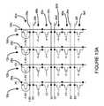
- FIG. 1Ais a schematic representation of a semiconductor DRAM array as illustrated (and described) in the Semiconductor Memory Device Patent Application;
- FIG. 1Billustrates a memory cell according to the Semiconductor Memory Device Patent Application
- FIGS. 2A and 2Bare exemplary schematic illustrations of the charge relationship, for a particular memory state, of the floating body, source and drain regions of a memory cell according to the Semiconductor Memory Device Patent Application;
- FIGS. 3A-3Care exemplary schematic and general illustrations of the charge relationship and charge pumping phenomenon caused by pulsing between positive and negative gate biases (during read and write operations) of the memory cell of FIG. 1B ;
- FIG. 4is a tabulation of exemplary voltage pulse levels that may be employed in a method of a first embodiment of the present invention
- FIG. 5is a tabulation of exemplary voltage pulse levels that may be employed in a method of a second embodiment of the present invention.
- FIG. 6is a tabulation of exemplary voltage pulse levels that may be employed in a method of a third embodiment of the present invention.
- FIG. 7is a tabulation of exemplary voltage pulse levels that may be employed in a method of an embodiment of the present invention.
- FIG. 8illustrates an exemplary word (gate) line voltage waveform to be used in a method of a fourth embodiment of the present invention
- FIG. 9illustrates an exemplary word (gate) line voltage waveform to be used in a method of a fifth embodiment of the present invention.
- FIG. 10illustrates a timing relationship between exemplary word (gate) line and the bit line voltage waveforms of the fourth embodiment of the present invention
- FIG. 11is a schematic representation of semiconductor DRAM memory device according to an aspect of present invention.
- FIG. 12is a schematic representation of column sense and refresh circuitry that may be employed in the semiconductor DRAM memory device of FIG. 11 ;
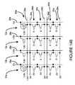
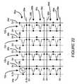
- FIGS. 13A, 13B , 14 A and 14 Billustrate a memory array including a plurality of memory cells having a separate source line array that define a particular row of memory cells, and exemplary writing and/or programming techniques (including exemplary programming voltage values), according to another aspect of the present invention
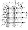
- FIGS. 15A and 15Billustrate read operations, including exemplary read operation voltage values, according to an embodiment of the present invention, for the memory array of FIGS. 13A, 13B , 14 A and 14 B;
- FIG. 16illustrates an exemplary layout of the memory array of FIGS. 13A, 13B , 14 A and 14 B;
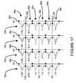
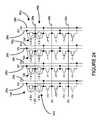
- FIGS. 17 and 18illustrate another memory array architecture including a plurality of memory cells having a common source line array, and writing and/or programming techniques (including exemplary programming voltage values), according to another aspect of the present invention
- FIG. 19illustrates exemplary read operation voltage values, according to an embodiment of the present invention, for the memory array of FIGS. 17 and 18 ;
- FIG. 20illustrates an exemplary layout of the memory array of FIGS. 17 and 18 ;
- FIG. 21illustrates a memory array including a plurality of memory cells having a separate source line array (that define a particular row of memory cells) and gates lines that are parallel to associated bit lines, and exemplary writing and/or programming techniques (including exemplary programming voltage values), according to another aspect of the present invention
- FIG. 22illustrates exemplary read operation voltage values, according to an embodiment of the present invention, for the memory array of FIG. 21 ;
- FIG. 23illustrates an exemplary layout of the memory array of FIGS. 21 and 22 ;
- FIGS. 24 and 25illustrate another memory array architecture including a plurality of memory cells having a common source line array, and writing and/or programming techniques (including exemplary programming voltage values), according to another aspect of the present invention
- FIG. 26illustrates exemplary read operation voltage values, according to an embodiment of the present invention, for a memory array of FIGS. 25 and 26 ;
- FIG. 27illustrates an exemplary layout of the memory array of FIGS. 24 and 25 ;
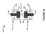
- FIG. 28illustrates an exemplary configuration of a dual-port or a multi-port memory cell, according to another aspect of the present invention.
- FIG. 29illustrates an exemplary layout of the dual-port or a multi-port memory cell of FIG. 28 .
- the present inventionis directed to a memory device and technique of reading data from and writing data into memory cells of the memory device.
- the memory device and technique for operating that devicethat minimizes, reduces and/or eliminates the debilitating affects of the charge pumping phenomenon.
- This embodiment of the present inventionemploys control signals that minimize, reduce and/or eliminate transitions of the amplitudes and/or polarities.
- transistor 14(a 0.25 micron N-channel MOSFET DRAM cell) may be operated using the exemplary voltage values.
- a write logic low (binary data state “0”) operationin one exemplary embodiment, may be written by applying a word line (i.e., gate bias) voltage of 2.9V, and the bit line (here, a drain bias) voltage of 2.3V. In this operation, the source line voltage is maintained at 0V. Under these conditions, the junction between body region 18 and source region 20 is forward biased, and excess holes are removed from body region 18 into source region 20 .
- a voltage of 0.6Vis applied to gate 16 (i.e., the gate bias is held at 0.6V) and a voltage of 2.3V is applied to drain 22 .
- an electric current between source region 20 and drain region 22providing impact ionization in body region 18 , which in turn generates excess majority carriers (holes) in body region 18 .
- the gate voltage of unselected cellsis kept at 0V. It is found that these exemplary voltages avoid strong accumulation of holes at the interface of gate oxide 32 and floating body region 18 wherein minority carriers 34 have a tendency to be “trapped” by or in defects within the semiconductor. In this way, disturbance of data caused by charge pumping is suppressed, reduced, minimized and/or eliminated.
- transistor 14(a 0.25 micron N-channel MOSFET DRAM cell) may be operated using the exemplary voltage values indicated.
- a logic highbinary data state “1”
- a strong accumulation of majority carriers at the interface of gate oxide 32 and floating body region 18is required.
- a voltage of ⁇ 1.7Vis applied to gate 16 and a voltage of 1.7V is applied to drain region 22 to provide the strong accumulation of majority carrier at the interface of gate oxide 32 and floating body region 18 .
- These control signalscause deformation of the valence and conduction bands at the interface between body region 18 and source region 20 .
- an inversion channelis created at the interface of gate oxide 32 and floating body region 18 . This may be achieved by applying a voltage of 0V to gate 16 and drain region 22 (i.e., a gate bias of 0V) and a voltage of ⁇ 0.5V to source region 20 .
- transistor 14(a 0.13 micron technology DRAM cell) may be programmed and/or operated using the exemplary voltages indicated.
- the voltages set forth in FIG. 6represent “ideal” conditions, in which the application of the voltage pulses does not disturb the data stored within the cell.
- the cellsare arranged in matrices in which some cells are accessed when others remain un-accessed, and column and row decoding are therefore necessary to enable the matrices to function. This results in voltage levels differing from the levels being applied during write, read and hold operations (in practice, all of the cells that share either the same column or row with the addressed memory cell), as a consequence of which disturbance of the data stored within those cells may occur.
- FIGS. 1 and 7An example of this is shown in FIGS. 1 and 7 , in which data state “0” is being written to memory cell 12 at the intersection of the selected word line and bit line. Since all cells in the same column of FIG. 1 share the same gate voltage and all cells in the same row as FIG. 7 share the same drain voltage, voltages different from the “ideal” holding voltages are applied to those memory cells, as a result of which charge may leak from the floating body regions of those cells.
- the number of word line drivers and/or sense amplifiersare reduced and/or minimized.
- a column decoderis disposed or arranged between the bit lines and the sense amplifiers to reduce and/or minimize the number of sense amplifiers and, in conjunction, while only one cell in a block (typically 8 or 16) is read.
- the memory cell on a column defined by an internal counter (for example, among 8 or 16) and on a row defined by user addressesis read and thereafter, refreshed. That cell then is available for user access (via read or write operation) at the same row and column defined by the user addresses.
- the variations or swings of the amplitude, as well as the polarity, of the gate voltagesare reduced and/or minimized in number and rising/falling edges.
- a read or write operation of a predetermined memory cellmay occur prior to the refresh operation. (See, for example, FIG. 9 ).
- the semiconductor DRAM memory device of this aspect of the present inventionincludes a plurality of matrices 40 a - n , each including a plurality of memory cells 12 (comprised of transistors 14 ).
- the memory cells 12are arranged in arrays having rows and columns, which may be addressed by content address memory (CAM) 42 and column refresh counter 44 .
- CAMcontent address memory
- the column address output from column refresh counter 44is applied to column address multiplexer 46 .
- the column address multiplexer 46receives the refresh address and the user address and provides one of the addresses to a column multiplexer 48 to select one of, for example, eight or sixteen bit lines (columns) 28 a.
- memory cell 12 at the intersection of a given or selected row and a given or selected columnis addressed by applying a signal on row address bus 50 to all of the interconnected gates of the row and a signal on column address bus 52 to all of the interconnected drains of the column.
- the row to be refreshedis identified by row refresh counter 54 , which is gated, via row address multiplexer 56 , with a row address from user address bus 58 .
- the column refresh counter 44supplies a column address of a column to be refreshed.
- the column addressis gated, via column address multiplexer 46 , with a column address from user address bus 58 .
- the column refresh counter 44may then increment in response to the same row being chosen, as a result of which the columns are sequentially addressed for each row, regardless of the order in which the rows are addressed. This provides the advantage of minimizing the risk that a memory cell 12 fails to be refreshed within the appropriate period.
- the column addressesare received from row refresh counter 44 or from user address bus 58 , and when, for example, the device (or portion thereof) is idle, the row addresses are provided by row refresh counter 54 .
- the refresh technique and circuitry of FIG. 11may be used with several arrays in parallel, as a result of which the number of sense amplifier 60 may be reduced and/or minimized (as is the area required for such circuitry on the die).
- the signal on WLDPW line 62provides a power supply voltage to word line drivers 62 a - x , according to the phase in the cycle waveform.
- the column multiplexer 48addresses the column (and therefore the selected memory cell) to be refreshed, and the data in the selected memory cell is read by sense amplifier 60 , the result being output (i.e., DATA signal) on signal line 66 .
- the write conditions applied to the word lineare as follows: During write “1” condition, if the DATA signal is “1”, XNOR logic gate 68 outputs, on signal line 68 , a logic high (i.e., binary “1”) which is amplified by write amplifier 72 and then applied to the selected memory cell in order to restore the data state in the selected memory cell. If the DATA signal is “0”, a logic low (i.e., “0”) is applied to the bit line, which represents a holding condition.
- the XNOR logic gate 68While writing data state “0”, on the other hand, if the DATA signal is “0”, the XNOR logic gate 68 outputs a logic high (i.e., binary “1”), which is amplified by write amplifier 72 and then applied to the memory cell to restore its data. If the DATA signal is “1”, a “0” is applied to the bit line, which again represents a holding condition.
- a two-step write operationmay be employed to program memory cell 12 with little to no disturbance to adjacent and/or neighboring cells (i.e., cells that share source lines, drain lines and/or gate lines).
- an entire row of memory cellsmay first be written to the same logic state and thereafter, individual bits are written to the opposite state in accordance with a desired data state (i.e., the individual bits are written to another state to reflect a desired data state).
- the write techniquemay be implemented where memory cells 12 a - d of each row 80 a - f of transistors have a dedicated source line to minimize, reduce and/or eliminate disturbance on adjacent rows (for example, row 80 b versus row 80 c ).
- a given row 80 a - fmay be written to by applying a clear operation followed by a selective write operation.
- a plurality of memory cells 100having gates that are connected to a common gate line, are arranged to form row 80 a .
- Exemplary voltages that implement a clear operation for row 80 a and maintain the remaining portion of the array (i.e., rows 80 b - f ) in a fixed state (i.e., unchanged in response to the clear operation)are indicated in FIGS. 13A and 13B .
- the same logic statefor example, logic high or binary “1”
- the state of memory cells 12 a - dare “cleared”.
- individual transistors of memory cells 12 a - d of row 80 aare written to a particular, desired and/or predetermined logic state (see, for example, FIGS. 14A and 14B ) in order to store the particular, desired and/or predetermined logic state in memory cells 12 a - d .
- memory cells 12 a - dare set to logic high (binary “1”) by the clear operation, and then memory cells 12 b and 12 d are written to logic low (binary “0”).
- the logic state of memory cells 12 a and 12 cremains logic high during the write operation (via applying an inhibit voltage to the associated bit lines 28 a and 28 c ( FIG. 14A ).
- memory cells 12 a - dare cleared to logic high (binary “1”) and then memory cells 12 a and 12 d are written to logic low (binary “0”).
- Memory cells 12 b and 12 cremain logic high via a write inhibit voltage applied to associated bit lines 28 b and 28 c.
- the datamay be read from memory cells 12 a - d of row 80 b by applying the exemplary voltages indicated.
- An exemplary holding voltage for the remaining portion of the array(including the memory cells of row 80 b - f ) is also indicated.
- the holding voltage/signalmaintains the unselected portion of the array in a fixed state (i.e., unchanged in response to the read operation).
- the exemplary read and holding voltages of FIGS. 15A and 15Bmay avoid, reduce and/or minimize charge pumping disturb.
- the first step of the write operationclears the memory cells having a common source line and the second step writes or stores new data or the previous data (in the event that the data did not change).
- Array architectures employing this write operation techniquemay have an advantage that the unselected memory cells of the array are not “disturbed” (or experience little and/or negligible disturbance) because “high” voltages are applied in the row direction (i.e., on source lines 26 ) but not in the column direction (i.e., on the drain or bit lines 28 ).
- This write techniquemay be performed as a page mode write where the page is first “cleared” and then individual bytes (or bits) in a page are written to a new state.
- FIGS. 13A, 13B , 14 A, 14 B, 15 A and 15 Bmay be implemented in conjunction with the embodiments of the device of FIGS. 11 and 12 .
- FIGS. 11 and 12For the sake of brevity, those discussions will not be repeated.
- FIGS. 17-20illustrate another memory array architecture in which a plurality of memory cells “share” a source line and employ the two-step write technique that may eliminate, minimize and/or reduce disturbance to memory cells when reading from and/or writing to adjacent memory cells.
- a given rowmay be written to by applying suitable voltages to implement a clear operation ( FIG. 17 ) followed by a selective write operation ( FIG. 18 ).
- a write inhibit signalis applied to the gates of memory cells that share a source line 26 (for example, a write inhibit signal may be applied to the gates of the memory cell of row 80 b ).
- any disturbance on unselected, adjacent row 80 bmay avoid, reduce and/or minimize by biasing word line 24 b to an intermediate value that balances write logic low (i.e., write “0”) and write logic high (i.e., write “1”) operation.
- exemplary voltages that implement a clear operation for row 80 a and maintain the neighboring memory cells (for example, memory cells of row 80 b ) remaining portion of the array in a fixed state (i.e., unchanged in response to the clear operation)are indicated in FIG. 17 .
- the memory cells 12 a - d of row 80 aare written to a particular, desired and/or predetermined logic state (see, for example, FIG. 18 (write “0”) in memory cell 12 a and memory cell 12 d and (write “1”) in memory cell 12 b and memory cell 12 c ) in order to store a particular, desired and/or predetermined logic state of memory cell 12 .
- the datamay be read from memory cells 12 a - d of row 80 a by applying the exemplary voltages indicated.
- an exemplary holding voltage for the remaining portion of the arrayis also indicated.
- the holding voltage/signalmaintains the unselected portion of the array in a fixed state (i.e., unchanged in response to the read or write operation).
- FIGS. 17-20may be implemented in conjunction with the embodiments of the device of FIGS. 11 and 12 .
- FIGS. 11 and 12For the sake of brevity, those discussions will not be repeated.
- FIGS. 21-23Another memory array architecture that may employ a one-step write technique that eliminates, minimizes and/or reduces disturbance to memory cells when reading from and/or writing to adjacent memory cells is illustrated in FIGS. 21-23 .
- source lines 26are separated for each row 80 a - e .
- word lines 24 a - dare arranged parallel to associated bit lines 28 a - d , respectively.
- a given rowmay be written to by applying suitable voltages to directly implement a write operation (see, memory cells 12 a - d of row 80 a ).
- a write inhibit signalis applied to source lines 26 b - e of rows 80 b - e , respectively.
- Exemplary voltages that implement the write operation (for memory cells 12 a - d ) and the inhibit state (for the memory cells of rows 80 b - e )are indicated in FIG. 21 .
- the memory cells 12 a and 12 d of row 80 aare maintained and/or written to a particular, desired and/or predetermined logic state (here, write “1”) and memory cells 12 b and 12 c are written to a different desired and/or predetermined logic state (here, write “0”).
- the datamay be read from memory cell 12 a of row 80 a by applying the exemplary voltages indicated.
- an exemplary read inhibit voltage for the remaining portion of the arrayis also indicated.
- the read inhibit voltage/signalmaintains the unselected portion of the array in a fixed state (i.e., unchanged in response to the read operation).
- FIGS. 21-23may be implemented in conjunction with the embodiments of the device of FIGS. 11 and 12 .
- FIGS. 11 and 12For the sake of brevity, those discussions will not be repeated.
- FIGS. 24-27Another memory array architecture that may employ the two-step write technique that eliminates, minimizes and/or reduces disturbance to memory cells when reading from and/or writing to adjacent memory cells is illustrated in FIGS. 24-27 .
- the source linesare shared but bit lines are separated so each memory cell on either side of a source line, for example memory cells 12 , has a dedicated bit line.
- the gates of transistors 12 a and 12 emay be connected together at the array boundary.
- memory cells 12 a and 12 eare located on separate rows with the gates of each transistor 12 a and 12 e connected at, for example, the array boundary.
- a given pair of rowsmay be written to by applying suitable voltage to implement a clear operation ( FIG. 24 ) followed by a selective write operation ( FIG. 25 ).
- the pair of rows(for example, rows 80 a and 80 b ) corresponding to memory cells 12 a and 12 e , on either side of a common source line, are written and read ( FIG. 26 ) simultaneously.
- FIGS. 24-27may be implemented in conjunction with the embodiments of the device of FIGS. 11 and 12 .
- those discussionswill not be repeated.
- the illustrated voltage levels to implement the write and read operationsare exemplary.
- the indicated voltage levelsmay be relative or absolute. That is, for example, a logic low may be written into transistor 102 a (see, for example, FIG. 13A ) using the voltages indicated therein.
- the voltages indicatedmay be relative in that each voltage level, for example, may be increased or decreased by a given voltage amount (for example, each voltage may be increased by 0.25 volts).
- the inventions (and embodiments thereof) described hereinare entirely applicable to P-channel transistors.
- majority carriers 30 in body region 18are electrons and minority carriers 34 are holes.
- the memory arrays of matrices 40 a - nmay be comprised of N-channel, P-channel and/or both types of transistors.
- the circuitry that is peripheral to the memory arraymay include P-channel and/or N-channel type transistors, including transistors like transistor 14 .
- memory cell(s) 12may also employ the structure, features, attributes, architectures, configurations, materials, techniques and advantages described and illustrated in non-provisional patent application entitled “Semiconductor Device”, which was filed on Feb. 18, 2004, by Fazan and Okhonin, and assigned Ser. No. 10/487,157 (hereinafter “Semiconductor Device Patent Application”).
- semiconductor Device Patent ApplicationThe entire contents of the Semiconductor Device Patent Application, including, for example, the inventions, features, attributes, architectures, configurations, materials, techniques and advantages described and illustrated therein, are hereby incorporated by reference herein.
- a dual port memory cell 12 amay include transistors 14 a and 14 b .
- a dual port memory arraymay include a plurality of dual port memory cells 12 arranged, for example, in a matrix of rows and columns. The data state defined by the amount of carriers in the common electrically floating body region 18 is common to the two transistors 14 a and 14 b.
- the read and write access operationsmay be performed independently for transistors 14 a or 14 b , using the respective independent word lines 24 , source line 26 and bit lines 28 .
- source line 26is common to the transistors 14 a and 14 b of memory cell 12 a .
- the source regions of transistors 14 a and 14 bmay be connected to separate source lines.
- dual port memory cell 12 aincludes a P+ floating body node 18 that “connects” a P ⁇ floating body region under gate 24 m of transistor 14 a with a P-floating body region under gate 24 n of transistor 14 b .
- the gates 24 m and 24 nare connected to word lines 24 m and 24 n , respectively.
- the source regions 20 a and 20 bare connected to respective source lines.
- the drain regions 22 a and 22 bare connected to drain lines.
- majority carriers in body region 18are electrons, and minority carriers are holes.
Landscapes
- Engineering & Computer Science (AREA)
- Microelectronics & Electronic Packaging (AREA)
- Computer Hardware Design (AREA)
- Manufacturing & Machinery (AREA)
- Dram (AREA)
- Semiconductor Memories (AREA)
Abstract
Description
- This application claims priority to: (1) U.S. Provisional Application Ser. No. 60/470,384, entitled “Method of Operating Semiconductor Memory Device”, filed May 13, 2003; and (2) U.S. Provisional Application Ser. No. 60/470,318, entitled “Dual Port One Transistor DRAM Memory Cell and Extension to Multi-Port Memory Cell”, filed May 13, 2003 (hereinafter collectively “the Provisional Applications”). The contents of the Provisional Applications are incorporated by reference herein in their entirety.
- This invention relates to a semiconductor dynamic random access memory (“DRAM”) cell, array and/or device and method of controlling and/or operating a semiconductor memory cell array and/or device; and more particularly, in one aspect, to a semiconductor dynamic random access memory (“DRAM”) cell, array and/or device wherein the memory cell includes an electrically floating body in which an electrical charge is stored.
- There are many different types and/or forms of DRAM cells, including, for example, a semiconductor memory cell consisting of an access transistor and a capacitor, which stores an electric charge representing a bi-stable memory state. The access transistor serves as a switch for controlling the charging and discharging of the capacitor as well as reading and writing of the logic states into the capacitor (i.e., charging or discharging the capacitor).
- Although significant integration densities can be achieved with DRAM devices employing one transistor—one capacitor memory cells, such devices tend to be limited or restricted with respect to the size of the memory cell. In this regard, conventional techniques employ stacked and/or trench capacitor approaches, whereby the capacitor is partially disposed above and/or below an access transistor.
- In addition, DRAM devices employing one transistor—one capacitor memory cells tend to be fabricated using manufacturing processes that are different from and/or incompatible with manufacturing processes for logic devices (for example, microprocessors). As a result, integration of one transistor—one capacitor memory cells into logic devices is often complicated and expensive.
- Another type of dynamic random access memory cell is described and illustrated in non-provisional patent application entitled “Semiconductor Device”, which was filed on Jun. 10, 2003, and assigned Ser. No. 10/450,238 (hereinafter “Semiconductor Memory Device Patent Application”). With reference to
FIGS. 1A and 1B , the Semiconductor Memory Device Patent Application discloses, among other things,semiconductor DRAM device 10 in which eachmemory cell 12 consists oftransistor 14 havinggate 16,body region 18, which is electrically floating,source region 20 anddrain region 22. Thebody region 18 is disposed between and adjacent tosource region 20 and drainregion 22. Data is written into or read from a selected memory cell by applying suitable control signals to a selected word line(s)24, a selected source line(s)26 and/or a selected bit line(s)28. In response, charge carriers are accumulated in or emitted and/or ejected from electrically floatingbody region 18 wherein the data states are defined by the amount of carriers within electrically floatingbody region 18. - In particular, in one embodiment, the memory cell of the Semiconductor Memory Device Patent Application operates by accumulating in or emitting/ejecting majority carriers (electrons or holes)30 from
body region 18 of N-channel transistors. (See,FIGS. 2A and 2B ). In this regard, accumulating majority carriers (in this example, “holes”)30 inbody region 18 ofmemory cells 12 via, for example, impact ionization nearsource region 20 and/ordrain region 22, is representative of a logic high or “1” data state. (See,FIG. 2A ). Emitting or ejectingmajority carriers 30 frombody region 18 via, for example, forward biasing the source/body junction and/or the drain/body junction, is representative of a logic low or “0”. (See,FIG. 2B ). - Various techniques may be employed to read the data stored in (or write the data into) a memory device of the Semiconductor Memory Device Patent Application. For example, a current sense amplifier (not illustrated) may be employed to read the data stored in
memory cells 12. In this regard, a current sense amplifier may compare the memory cell current to a reference current, for example, the current of a reference cell (not illustrated). From that comparison, it may be determined whethermemory cell 12 contained a logic high (relativelymore majority carriers 30 contained within body region18) or logic low data state (relativelyless majority carriers 28 contained within body region18). - Notably,
transistor 14 may be a symmetrical or non-symmetrical device. Wheretransistor 14 is symmetrical, the source and drain regions are essentially interchangeable. However, wheretransistor 14 is a non-symmetrical device, the source or drain regions oftransistor 14 have different electrical, physical, doping concentration and/or doping profile characteristics. As such, the source or drain regions of a non-symmetrical device are typically not interchangeable. - The
transistor 14 may be controlled using a negative drain voltage on, for example, bit line28i, to remove holes from electrically floatingbody region 18 throughdrain 22 to write a logic low (i.e., binary state “0”). Under this circumstances, a negative voltage applied togate 16 of the other (non-selected) memory cells in the memory array ofdevice 10 may be necessary to avoid “leakage current” in other cells connected to the same bit line28iwhen the negative bit line voltage is applied during the write (logic low) operation. - Other operations such as writing a logic high data state (binary “1”) and reading the data may be performed using positive voltages applied to
word lines 24. As such,transistors 14 ofdevice 10 are periodically pulsed between a positive gate bias, which (1) drives majority carriers (holes for N-channel transistors) away from the interface betweengate insulator 32 andbody region 18 oftransistor 14 and (2) causes minority carriers (electrons for N-channel transistors) to flow fromsource region 20 anddrain region 22 into a channel formed belowgate 16, and a negative gate bias, which causes majority carriers (holes for N-channel transistors) to accumulate in or near the interface betweengate 16 andbody region 18 oftransistor 14. - With reference to
FIG. 3A , a positive voltage applied togate 16 provides a positive gate bias which causes (1) a channel ofminority carriers 34 to form beneathgate 16 and (2) accumulation ofmajority carriers 30 inbody region 18 in an area “opposite” the interface ofgate 16 andbody region 18. Here, minority carriers (i.e., electrons in an N-channel transistor) may flow in the channel beneath the interface ofgate oxide 32 and floatingbody region 18 wherein some of theminority carriers 34 are “trapped” by or in defects within the semiconductor (typically created or caused by the transition from one material type to another). - With reference to
FIG. 3B , when a negative voltage is applied togate 16, the gate bias is negative which substantially eliminates the channel ofminority carriers 34 beneath gate16 (and gate oxide34). However, some of minority carriers may remain “trapped” in the interface defects (illustrated generally by electrons36). - Some of the trapped
electrons 36 recombine with majority carriers which are attracted to gate16 (due to the negative gate bias), and, as such, the net charge ofmajority carriers 30 located infloating body region 18 may decrease over time (see, for example,FIG. 3C ). This phenomenon may be characterized as charge pumping. Thus, pulsing between positive and negative gate biases (during read and write operations) may reduce the net quantity of charge inmemory cell 12, which, in turn, may gradually eliminate the data stored inmemory cell 12. - Notably, for the efficient charge pumping phenomenon to occur, the free electron concentration at the surface (ne) in inversion should be sufficiently large that the interface traps can capture electrons during the time the transistor is in inversion. The time constant for electron capture may be characterized as:
- Accordingly, in the case τe=3 ns (typical pulse duration in advanced DRAM memories), the thermal velocity νth=1×107cm/s and the capture cross section σ=2×10⁻¹⁶cm2, at least
n e2≈1017cm−3may be required. Analogously, in accumulation the free hole concentration at the surface (nh) should be sufficiently large that holes can recombine with the captured electrons during thetime transistor 14 is in accumulation. If σn=σp,n h2≈1017cm−3at least may be required (i.e., the efficient charge pumping effect exists if the gate voltage in inversion accumulates at least 2×1017cm−3electrons at the surface and the gate voltage in accumulation accumulates at least 2×1017cm−3holes). - Notably, the entire contents of the Semiconductor Memory Device Patent Application, including, for example, the features, attributes, architectures, configurations, materials, techniques and advantages described and illustrated therein, are incorporated by reference herein.
- There are many inventions described and illustrated herein. In a first principal aspect, the present invention is a semiconductor memory array comprising a plurality of semiconductor dynamic random access memory cells arranged in a matrix of rows and columns. Each semiconductor dynamic random access memory cell includes a transistor having a source region, a drain region, a electrically floating body region disposed between and adjacent to the source region and the drain region, and a gate spaced apart from, and capacitively coupled to, the body region. Each transistor includes a first state representative of a first charge in the body region, and a second data state representative of a second charge in the body region. Further, each row of semiconductor dynamic random access memory cells includes an associated source line which is connected to only the semiconductor dynamic random access memory cells of the associated row.
- In one embodiment of this aspect of the present invention, each memory cell of each row of semiconductor dynamic random access memory cells includes a separate bit line which is connected to the drain region of the associated transistor. In operation, each memory cell of a first row is programmed to a first data state by applying a control signal, having a first amplitude, to the gate of the transistor of each memory cell of the first row and a control signal, having a second amplitude, to the drain of each memory cell of the first row. Thereafter, a predetermined memory cell of the first row may be programmed to a second data state by applying a control signal, having a third amplitude, to the gate of the transistor of the predetermined memory cell, a control signal, having an fourth amplitude, to the drain of predetermined memory cell, and a control signal, having a fifth amplitude, to the source of predetermined memory cell of the row. Notably, unselected memory cell(s) of the first row is/are maintained in the first data state, while the predetermined memory cell is programmed to a second data state, by applying a control signal, having a third amplitude, to the gate of the transistor of the predetermined memory cell and a control signal, having an sixth amplitude, to the drain of predetermined memory cell.
- The memory cells of the first row may be read by applying a control signal, having a seventh amplitude, to the gate of the transistor of the predetermined memory cell and a control signal, having an eighth amplitude, to the drain of predetermined memory cell. Notably, all of the memory cells of a second row (an unselected row) are maintained in an inhibit state while the memory cells of the first row are read. In one embodiment, the memory cells of the second row are maintained in an inhibit state (while the memory cells of the first row are read) by applying a control signal having a ninth amplitude to the gate of the transistors of the memory cells of the second row.
- In one embodiment, the each memory cell of a first row of semiconductor dynamic random access memory cells shares a drain region with a memory cell in a second row of semiconductor dynamic random access memory cells, wherein the first and second rows of memory cells are adjacent rows. In another embodiment, each gate of each memory cell of a first row of semiconductor dynamic random access memory cells is connected to a first gate line. In yet another embodiment, the gate of each memory cell of the first row of semiconductor dynamic random access memory cells is connected to the first gate line.
- In another principal aspect, the present invention is a semiconductor memory array comprising a plurality of semiconductor dynamic random access memory cells arranged in a matrix of rows and columns. Again, each semiconductor dynamic random access memory cell includes a transistor having a source region, a drain region, a electrically floating body region disposed between and adjacent to the source region and the drain region, and a gate spaced apart from, and capacitively coupled to, the body region. Each transistor includes a first state representative of a first charge in the body region, and a second data state representative of a second charge in the body region.
- In this aspect, the each row of semiconductor dynamic random access memory cells includes (1) an associated source line which is connected to only the semiconductor dynamic random access memory cells in the associated row and (2) a different gate line for each semiconductor dynamic random access memory cells in the associated row.
- In one embodiment of this aspect of the present invention, each memory cell of each row of semiconductor dynamic random access memory cells includes a separate bit line which is connected to the drain region of the associated transistor. In operation, each memory cell of a first row is programmed to a first data state by applying a control signal, having a first amplitude, to the gate of the transistor of each memory cell of the first row and a control signal, having a second amplitude, to the drain of each memory cell of the first row. Thereafter, a predetermined memory cell of the first row may be programmed to a second data state by applying a control signal, having a third amplitude, to the gate of the transistor of the predetermined memory cell, a control signal, having a fourth amplitude, to the drain of predetermined memory cell, and a control signal, having a fifth amplitude, to the source of predetermined memory cell of the row. Notably, unselected memory cell(s) of the first row is/are maintained in the first data state, while the predetermined memory cell is programmed to a second data state, by applying a control signal, having a third amplitude, to the gate of the transistor of the predetermined memory cell and a control signal, having a sixth amplitude, to the drain of predetermined memory cell.
- The memory cells of the first row may be read by applying a control signal, having a seventh amplitude, to the gate of the transistor of the predetermined memory cell and a control signal, having an eighth amplitude, to the drain of predetermined memory cell. Notably, all of the memory cells of a second row (an unselected row) are maintained in an inhibit state while the memory cells of the first row are read. In one embodiment, the memory cells of the second row are maintained in an inhibit state (while the memory cells of the first row are read) by applying a control signal having a ninth amplitude to the gate of the transistors of the memory cells of the second row.
- In one embodiment, the each memory cell of a first row of semiconductor dynamic random access memory cells shares a drain region with a memory cell in a second row of semiconductor dynamic random access memory cells, wherein the first and second rows of memory cells are adjacent rows. In another embodiment, each gate of each memory cell of a first row of semiconductor dynamic random access memory cells is connected to a first gate line.
- Again, there are many inventions described and illustrated herein. This Summary of the Invention is not exhaustive of the scope of the present invention. Moreover, this Summary is not intended to be limiting of the invention and should not be interpreted in that manner. While certain embodiments, features, attributes and advantages of the inventions have been described in this Summary, it should be understood that many others, as well as different and/or similar embodiments, features, attributes and/or advantages of the present inventions, which are apparent from the description, illustrations and claims, which follow.
- In the course of the detailed description to follow, reference will be made to the attached drawings. These drawings show different aspects of the present invention and, where appropriate, reference numerals illustrating like structures, components, materials and/or elements in different figures are labeled similarly. It is understood that various combinations of the structures, components, materials and/or elements, other than those specifically shown, are contemplated and are within the scope of the present invention.
FIG. 1A is a schematic representation of a semiconductor DRAM array as illustrated (and described) in the Semiconductor Memory Device Patent Application;FIG. 1B illustrates a memory cell according to the Semiconductor Memory Device Patent Application;FIGS. 2A and 2B are exemplary schematic illustrations of the charge relationship, for a particular memory state, of the floating body, source and drain regions of a memory cell according to the Semiconductor Memory Device Patent Application;FIGS. 3A-3C are exemplary schematic and general illustrations of the charge relationship and charge pumping phenomenon caused by pulsing between positive and negative gate biases (during read and write operations) of the memory cell ofFIG. 1B ;FIG. 4 is a tabulation of exemplary voltage pulse levels that may be employed in a method of a first embodiment of the present invention;FIG. 5 is a tabulation of exemplary voltage pulse levels that may be employed in a method of a second embodiment of the present invention;FIG. 6 is a tabulation of exemplary voltage pulse levels that may be employed in a method of a third embodiment of the present invention;FIG. 7 is a tabulation of exemplary voltage pulse levels that may be employed in a method of an embodiment of the present invention;FIG. 8 illustrates an exemplary word (gate) line voltage waveform to be used in a method of a fourth embodiment of the present invention;FIG. 9 illustrates an exemplary word (gate) line voltage waveform to be used in a method of a fifth embodiment of the present invention;FIG. 10 illustrates a timing relationship between exemplary word (gate) line and the bit line voltage waveforms of the fourth embodiment of the present invention;FIG. 11 is a schematic representation of semiconductor DRAM memory device according to an aspect of present invention;FIG. 12 is a schematic representation of column sense and refresh circuitry that may be employed in the semiconductor DRAM memory device ofFIG. 11 ;FIGS. 13A, 13B ,14A and14B illustrate a memory array including a plurality of memory cells having a separate source line array that define a particular row of memory cells, and exemplary writing and/or programming techniques (including exemplary programming voltage values), according to another aspect of the present invention;FIGS. 15A and 15B illustrate read operations, including exemplary read operation voltage values, according to an embodiment of the present invention, for the memory array ofFIGS. 13A, 13B ,14A and14B;FIG. 16 illustrates an exemplary layout of the memory array ofFIGS. 13A, 13B ,14A and14B;FIGS. 17 and 18 illustrate another memory array architecture including a plurality of memory cells having a common source line array, and writing and/or programming techniques (including exemplary programming voltage values), according to another aspect of the present invention;FIG. 19 illustrates exemplary read operation voltage values, according to an embodiment of the present invention, for the memory array ofFIGS. 17 and 18 ;FIG. 20 illustrates an exemplary layout of the memory array ofFIGS. 17 and 18 ;FIG. 21 illustrates a memory array including a plurality of memory cells having a separate source line array (that define a particular row of memory cells) and gates lines that are parallel to associated bit lines, and exemplary writing and/or programming techniques (including exemplary programming voltage values), according to another aspect of the present invention;FIG. 22 illustrates exemplary read operation voltage values, according to an embodiment of the present invention, for the memory array ofFIG. 21 ;FIG. 23 illustrates an exemplary layout of the memory array ofFIGS. 21 and 22 ;FIGS. 24 and 25 illustrate another memory array architecture including a plurality of memory cells having a common source line array, and writing and/or programming techniques (including exemplary programming voltage values), according to another aspect of the present invention;FIG. 26 illustrates exemplary read operation voltage values, according to an embodiment of the present invention, for a memory array ofFIGS. 25 and 26 ;FIG. 27 illustrates an exemplary layout of the memory array ofFIGS. 24 and 25 ;FIG. 28 illustrates an exemplary configuration of a dual-port or a multi-port memory cell, according to another aspect of the present invention; andFIG. 29 illustrates an exemplary layout of the dual-port or a multi-port memory cell ofFIG. 28 .- There are many inventions described and illustrated herein. In a first aspect, the present invention is directed to a memory device and technique of reading data from and writing data into memory cells of the memory device. In this regard, in one embodiment of this aspect of the invention, the memory device and technique for operating that device that minimizes, reduces and/or eliminates the debilitating affects of the charge pumping phenomenon. This embodiment of the present invention employs control signals that minimize, reduce and/or eliminate transitions of the amplitudes and/or polarities.
- With reference to
FIGS. 1 and 4 , in one embodiment, transistor14 (a 0.25 micron N-channel MOSFET DRAM cell) may be operated using the exemplary voltage values. In this regard, a write logic low (binary data state “0”) operation, in one exemplary embodiment, may be written by applying a word line (i.e., gate bias) voltage of 2.9V, and the bit line (here, a drain bias) voltage of 2.3V. In this operation, the source line voltage is maintained at 0V. Under these conditions, the junction betweenbody region 18 andsource region 20 is forward biased, and excess holes are removed frombody region 18 intosource region 20. - To perform a write logic high (binary data state “1”) in
transistor 14, a voltage of 0.6V is applied to gate16 (i.e., the gate bias is held at 0.6V) and a voltage of 2.3V is applied to drain22. In response, an electric current betweensource region 20 and drainregion 22 providing impact ionization inbody region 18, which in turn generates excess majority carriers (holes) inbody region 18. Note that the gate voltage of unselected cells (holding voltage) is kept at 0V. It is found that these exemplary voltages avoid strong accumulation of holes at the interface ofgate oxide 32 and floatingbody region 18 whereinminority carriers 34 have a tendency to be “trapped” by or in defects within the semiconductor. In this way, disturbance of data caused by charge pumping is suppressed, reduced, minimized and/or eliminated. - In a second embodiment, with reference to
FIGS. 1 and 5 , transistor14 (a 0.25 micron N-channel MOSFET DRAM cell) may be operated using the exemplary voltage values indicated. In this regard, to write a logic high (binary data state “1”), a strong accumulation of majority carriers at the interface ofgate oxide 32 and floatingbody region 18 is required. In one exemplary embodiment, a voltage of −1.7V is applied togate 16 and a voltage of 1.7V is applied to drainregion 22 to provide the strong accumulation of majority carrier at the interface ofgate oxide 32 and floatingbody region 18. These control signals cause deformation of the valence and conduction bands at the interface betweenbody region 18 andsource region 20. As a result, minority carriers (here, electrons) are injected into the conduction band by means of a tunnel effect (an effect known as gate induced drain leakage (GIDL)), which in turn causes the generation of majority carriers (here, holes) inbody region 18. This operating technique has an advantage in that hole generation occurs in a non-conducting state oftransistor 14. In this way, majority carrier generation may be achieved at a relatively lower power consumption. - To perform a read data operation, in one embodiment, an inversion channel is created at the interface of
gate oxide 32 and floatingbody region 18. This may be achieved by applying a voltage of 0V togate 16 and drain region22 (i.e., a gate bias of 0V) and a voltage of −0.5V to sourceregion 20. - In a third embodiment, with reference to
FIGS. 1 and 6 , transistor14 (a 0.13 micron technology DRAM cell) may be programmed and/or operated using the exemplary voltages indicated. The voltages set forth inFIG. 6 represent “ideal” conditions, in which the application of the voltage pulses does not disturb the data stored within the cell. However, the cells are arranged in matrices in which some cells are accessed when others remain un-accessed, and column and row decoding are therefore necessary to enable the matrices to function. This results in voltage levels differing from the levels being applied during write, read and hold operations (in practice, all of the cells that share either the same column or row with the addressed memory cell), as a consequence of which disturbance of the data stored within those cells may occur. - An example of this is shown in
FIGS. 1 and 7 , in which data state “0” is being written tomemory cell 12 at the intersection of the selected word line and bit line. Since all cells in the same column ofFIG. 1 share the same gate voltage and all cells in the same row asFIG. 7 share the same drain voltage, voltages different from the “ideal” holding voltages are applied to those memory cells, as a result of which charge may leak from the floating body regions of those cells. - Similar arrangements occur when writing logic high (i.e., data state “1”) or reading the data from
memory cells 12. It is found (experimentally) that a worst case is represented by writing logic low (i.e., data state “0”), andmemory cells 14 may sustain a few hundred cycles of word line switching, and over 10,000 cycles of bit line switching. It can therefore be seen that fluctuations in the gate voltage may impose limitations on the architecture of the circuit, and in particular, if it is assumed that only 100 cycles of word line pulsing are permissible, this small number of cycles could either necessitate partitioning the rows to smaller length (e.g., 64) or refreshing all cells along the word line as frequently as on a prior art DRAM involving transistors and capacitors. - Both of these arrangements are extremely inefficient since they could significantly increase the number of word line drivers or sense amplifiers required to operate the circuit. Furthermore, because each data cell is smaller (4F2) than a conventional DRAM cell (8F2), the circuit layout may be either impossible or extremely expensive to achieve.
- With reference to
FIGS. 8, 11 and12, in one embodiment, the number of word line drivers and/or sense amplifiers are reduced and/or minimized. In this regard, a column decoder is disposed or arranged between the bit lines and the sense amplifiers to reduce and/or minimize the number of sense amplifiers and, in conjunction, while only one cell in a block (typically 8 or 16) is read. The memory cell on a column defined by an internal counter (for example, among 8 or 16) and on a row defined by user addresses is read and thereafter, refreshed. That cell then is available for user access (via read or write operation) at the same row and column defined by the user addresses. - From a signaling perspective, with reference to
FIG. 8 , the variations or swings of the amplitude, as well as the polarity, of the gate voltages are reduced and/or minimized in number and rising/falling edges. Notably, a read or write operation of a predetermined memory cell may occur prior to the refresh operation. (See, for example,FIG. 9 ). - With reference to
FIGS. 11 and 12 , the semiconductor DRAM memory device of this aspect of the present invention includes a plurality of matrices40a-n, each including a plurality of memory cells12 (comprised of transistors14). Thememory cells 12 are arranged in arrays having rows and columns, which may be addressed by content address memory (CAM)42 andcolumn refresh counter 44. The column address output fromcolumn refresh counter 44 is applied tocolumn address multiplexer 46. Thecolumn address multiplexer 46 receives the refresh address and the user address and provides one of the addresses to acolumn multiplexer 48 to select one of, for example, eight or sixteen bit lines (columns)28a. - In order to enable
memory cells 12 to be refreshed during, for example, idle periods (i.e., when there is no user access),memory cell 12 at the intersection of a given or selected row and a given or selected column is addressed by applying a signal onrow address bus 50 to all of the interconnected gates of the row and a signal oncolumn address bus 52 to all of the interconnected drains of the column. The row to be refreshed is identified byrow refresh counter 54, which is gated, viarow address multiplexer 56, with a row address fromuser address bus 58. - The
column refresh counter 44 supplies a column address of a column to be refreshed. As mentioned above, the column address is gated, viacolumn address multiplexer 46, with a column address fromuser address bus 58. As a result, the data state ofmemory cell 12 at the intersection of the selected row and column is determined and re-written tomemory cell 12. Thecolumn refresh counter 44 may then increment in response to the same row being chosen, as a result of which the columns are sequentially addressed for each row, regardless of the order in which the rows are addressed. This provides the advantage of minimizing the risk that amemory cell 12 fails to be refreshed within the appropriate period. Depending on the phase during access, the column addresses are received fromrow refresh counter 44 or fromuser address bus 58, and when, for example, the device (or portion thereof) is idle, the row addresses are provided byrow refresh counter 54. - Notably, the refresh technique and circuitry of
FIG. 11 may be used with several arrays in parallel, as a result of which the number ofsense amplifier 60 may be reduced and/or minimized (as is the area required for such circuitry on the die). - With reference to
FIG. 12 , when a column is selected, the signal onWLDPW line 62 provides a power supply voltage toword line drivers 62a-x, according to the phase in the cycle waveform. Thecolumn multiplexer 48 addresses the column (and therefore the selected memory cell) to be refreshed, and the data in the selected memory cell is read bysense amplifier 60, the result being output (i.e., DATA signal) on signal line66. - According to the signal logic levels on line62 (after conversion by voltage converter68) and line66, the write conditions applied to the word line are as follows: During write “1” condition, if the DATA signal is “1”,
XNOR logic gate 68 outputs, onsignal line 68, a logic high (i.e., binary “1”) which is amplified bywrite amplifier 72 and then applied to the selected memory cell in order to restore the data state in the selected memory cell. If the DATA signal is “0”, a logic low (i.e., “0”) is applied to the bit line, which represents a holding condition. While writing data state “0”, on the other hand, if the DATA signal is “0”, theXNOR logic gate 68 outputs a logic high (i.e., binary “1”), which is amplified bywrite amplifier 72 and then applied to the memory cell to restore its data. If the DATA signal is “1”, a “0” is applied to the bit line, which again represents a holding condition. - In certain embodiments, it may be advantageous to further reduce, minimize and/or eliminate any issues of disturbance (for example, issues of stored charge loss orgain within memory cells) of the data states of memory cells having common gate lines, drain lines and/or source lines with those memory cells that are being accessed (i.e., being read from or written to during, for example, a normal or refresh operation). In one embodiment, a two-step write operation may be employed to
program memory cell 12 with little to no disturbance to adjacent and/or neighboring cells (i.e., cells that share source lines, drain lines and/or gate lines). In this regard, an entire row of memory cells may first be written to the same logic state and thereafter, individual bits are written to the opposite state in accordance with a desired data state (i.e., the individual bits are written to another state to reflect a desired data state). - It is intended that such two step write technique may be employed using many different memory cells and many different memory array architectures, whether now known or later developed; and all such memory cells and different memory array architectures fall within the present invention. For example, the write technique may be implemented where
memory cells 12a-dof each row80a-fof transistors have a dedicated source line to minimize, reduce and/or eliminate disturbance on adjacent rows (for example,row 80bversusrow 80c). - With reference to
FIGS. 13A and 13B , in one embodiment, a given row80a-fmay be written to by applying a clear operation followed by a selective write operation. In this regard, a plurality of memory cells100, having gates that are connected to a common gate line, are arranged to formrow 80a. Exemplary voltages that implement a clear operation forrow 80aand maintain the remaining portion of the array (i.e.,rows 80b-f) in a fixed state (i.e., unchanged in response to the clear operation) are indicated inFIGS. 13A and 13B . In response, the same logic state (for example, logic high or binary “1”) is stored inmemory cells 12a-dofrow 80a. In this way, the state ofmemory cells 12a-dare “cleared”. - Thereafter, individual transistors of
memory cells 12a-dofrow 80aare written to a particular, desired and/or predetermined logic state (see, for example,FIGS. 14A and 14B ) in order to store the particular, desired and/or predetermined logic state inmemory cells 12a-d. In particular, with reference toFIG. 14A , as described above,memory cells 12a-dare set to logic high (binary “1”) by the clear operation, and thenmemory cells memory cells bit lines FIG. 14A ). With reference toFIG. 14B ,memory cells 12a-dare cleared to logic high (binary “1”) and thenmemory cells Memory cells bit lines - With reference to
FIGS. 15A and 15B , the data may be read frommemory cells 12a-dofrow 80bby applying the exemplary voltages indicated. An exemplary holding voltage for the remaining portion of the array (including the memory cells ofrow 80b-f) is also indicated. The holding voltage/signal maintains the unselected portion of the array in a fixed state (i.e., unchanged in response to the read operation). Notably, the exemplary read and holding voltages ofFIGS. 15A and 15B may avoid, reduce and/or minimize charge pumping disturb. - Thus, in this embodiment, the first step of the write operation clears the memory cells having a common source line and the second step writes or stores new data or the previous data (in the event that the data did not change). Array architectures employing this write operation technique may have an advantage that the unselected memory cells of the array are not “disturbed” (or experience little and/or negligible disturbance) because “high” voltages are applied in the row direction (i.e., on source lines26) but not in the column direction (i.e., on the drain or bit lines28). This write technique may be performed as a page mode write where the page is first “cleared” and then individual bytes (or bits) in a page are written to a new state.
- Notably, the memory architecture, write and/or programming techniques, and read techniques of
FIGS. 13A, 13B ,14A,14B,15A and15B may be implemented in conjunction with the embodiments of the device ofFIGS. 11 and 12 . For the sake of brevity, those discussions will not be repeated. FIGS. 17-20 illustrate another memory array architecture in which a plurality of memory cells “share” a source line and employ the two-step write technique that may eliminate, minimize and/or reduce disturbance to memory cells when reading from and/or writing to adjacent memory cells. In this regard, with reference toFIGS. 17 and 18 , in one embodiment, a given row may be written to by applying suitable voltages to implement a clear operation (FIG. 17 ) followed by a selective write operation (FIG. 18 ). In conjunction with applying suitable voltages to implement the clear operation, a write inhibit signal is applied to the gates of memory cells that share a source line26 (for example, a write inhibit signal may be applied to the gates of the memory cell ofrow 80b). Notably, any disturbance on unselected,adjacent row 80b(with respect to row80a), may avoid, reduce and/or minimize by biasingword line 24bto an intermediate value that balances write logic low (i.e., write “0”) and write logic high (i.e., write “1”) operation.- In particular, exemplary voltages that implement a clear operation for
row 80aand maintain the neighboring memory cells (for example, memory cells ofrow 80b) remaining portion of the array in a fixed state (i.e., unchanged in response to the clear operation) are indicated inFIG. 17 . Thememory cells 12a-dofrow 80aare written to a particular, desired and/or predetermined logic state (see, for example,FIG. 18 (write “0”) inmemory cell 12aandmemory cell 12dand (write “1”) inmemory cell 12bandmemory cell 12c) in order to store a particular, desired and/or predetermined logic state ofmemory cell 12. - With reference to
FIG. 19 , the data may be read frommemory cells 12a-dofrow 80aby applying the exemplary voltages indicated. Notably, an exemplary holding voltage for the remaining portion of the array (including the neighboring memory cells ofrow 80bas well as the memory cells ofrows 80c-f) is also indicated. The holding voltage/signal maintains the unselected portion of the array in a fixed state (i.e., unchanged in response to the read or write operation). - The memory architecture, write and/or programming techniques, and read techniques of
FIGS. 17-20 may be implemented in conjunction with the embodiments of the device ofFIGS. 11 and 12 . For the sake of brevity, those discussions will not be repeated. - Another memory array architecture that may employ a one-step write technique that eliminates, minimizes and/or reduces disturbance to memory cells when reading from and/or writing to adjacent memory cells is illustrated in
FIGS. 21-23 . In this architecture, source lines26 are separated for each row80a-e. In addition,word lines 24a-dare arranged parallel to associatedbit lines 28a-d, respectively. - With reference to
FIG. 21 , in one embodiment, a given row may be written to by applying suitable voltages to directly implement a write operation (see,memory cells 12a-dofrow 80a). In conjunction with applying suitable voltages to implement the write operation, a write inhibit signal is applied tosource lines 26b-eofrows 80b-e, respectively. Exemplary voltages that implement the write operation (formemory cells 12a-d) and the inhibit state (for the memory cells ofrows 80b-e) are indicated inFIG. 21 . Thememory cells row 80aare maintained and/or written to a particular, desired and/or predetermined logic state (here, write “1”) andmemory cells - With reference to
FIG. 22 , the data may be read frommemory cell 12aofrow 80aby applying the exemplary voltages indicated. Notably, an exemplary read inhibit voltage for the remaining portion of the array (including the other memory cells ofrow 80aand the memory cells ofrows 80d-e) is also indicated. The read inhibit voltage/signal maintains the unselected portion of the array in a fixed state (i.e., unchanged in response to the read operation). - The memory architecture, write and/or programming techniques, and read techniques of
FIGS. 21-23 may be implemented in conjunction with the embodiments of the device ofFIGS. 11 and 12 . For the sake of brevity, those discussions will not be repeated. - Another memory array architecture that may employ the two-step write technique that eliminates, minimizes and/or reduces disturbance to memory cells when reading from and/or writing to adjacent memory cells is illustrated in
FIGS. 24-27 . In this architecture, the source lines are shared but bit lines are separated so each memory cell on either side of a source line, forexample memory cells 12, has a dedicated bit line. The gates oftransistors - Notably,
memory cells transistor drain lines memory cell transistor - With reference to
FIGS. 24-27 , in one embodiment, a given pair of rows may be written to by applying suitable voltage to implement a clear operation (FIG. 24 ) followed by a selective write operation (FIG. 25 ). The pair of rows (for example,rows memory cells FIG. 26 ) simultaneously. - Notably, the memory architecture, write and/or programming techniques, and read techniques of
FIGS. 24-27 may be implemented in conjunction with the embodiments of the device ofFIGS. 11 and 12 . For the sake of brevity, those discussions will not be repeated. - There are many inventions described and illustrated herein. While certain embodiments, features, materials, configurations, attributes and advantages of the inventions have been described and illustrated, it should be understood that many other, as well as different and/or similar embodiments, features, materials, configurations, attributes, structures and advantages of the present inventions that are apparent from the description, illustration and claims. As such, the embodiments, features, materials, configurations, attributes, structures and advantages of the inventions described and illustrated herein are not exhaustive and it should be understood that such other, similar, as well as different, embodiments, features, materials, configurations, attributes, structures and advantages of the present inventions are within the scope of the present invention.
- For example, as mentioned above, the illustrated voltage levels to implement the write and read operations are exemplary. The indicated voltage levels may be relative or absolute. That is, for example, a logic low may be written into transistor102a(see, for example,
FIG. 13A ) using the voltages indicated therein. Alternatively, the voltages indicated may be relative in that each voltage level, for example, may be increased or decreased by a given voltage amount (for example, each voltage may be increased by 0.25 volts). - Moreover, while a significant portion of this description includes details (for example, clear, write, read and inhibit voltages) directed to N-channel transistors, the inventions (and embodiments thereof) described herein are entirely applicable to P-channel transistors. In such embodiments,
majority carriers 30 inbody region 18 are electrons andminority carriers 34 are holes. Indeed, the memory arrays of matrices40a-nmay be comprised of N-channel, P-channel and/or both types of transistors. Moreover, the circuitry that is peripheral to the memory array (for example, row and column address decoders, not illustrated herein, as well as comparators) may include P-channel and/or N-channel type transistors, including transistors liketransistor 14. - Notably, where P-channel type transistors are employed as
memory cells 12 in the memory array(s) of matrices40a-n, suitable clear, write, read and inhibit voltages are well known to those skilled in the art in light of this disclosure. Accordingly, for sake of brevity, these discussions will not be repeated. - Further, memory cell(s)12 (as well as memory array and matrices40a-n) may also employ the structure, features, attributes, architectures, configurations, materials, techniques and advantages described and illustrated in non-provisional patent application entitled “Semiconductor Device”, which was filed on Feb. 18, 2004, by Fazan and Okhonin, and assigned Ser. No. 10/487,157 (hereinafter “Semiconductor Device Patent Application”). The entire contents of the Semiconductor Device Patent Application, including, for example, the inventions, features, attributes, architectures, configurations, materials, techniques and advantages described and illustrated therein, are hereby incorporated by reference herein.
- Furthermore, the memory transistors and/or cells, and method of operating such transistors and/or cells, of the present invention may be implemented in many different configurations. For example, the floating body regions of two or more transistors may be shared to realize a dual-port or a multi-port memory cell. In this regard, with reference to
FIG. 28 , a dualport memory cell 12amay includetransistors port memory cells 12 arranged, for example, in a matrix of rows and columns. The data state defined by the amount of carriers in the common electrically floatingbody region 18 is common to the twotransistors - The read and write access operations may be performed independently for
transistors source line 26 and bit lines28. In the illustrative example,source line 26 is common to thetransistors memory cell 12a. Notably, the source regions oftransistors - With reference to
FIG. 29 , in an exemplary layout, dualport memory cell 12aincludes a P+ floatingbody node 18 that “connects” a P− floating body region undergate 24moftransistor 14awith a P-floating body region undergate 24noftransistor 14b. Thegates word lines source regions drain regions body region 18 are electrons, and minority carriers are holes.
Claims (22)
Priority Applications (1)
| Application Number | Priority Date | Filing Date | Title |
|---|---|---|---|
| US11/096,970US7085156B2 (en) | 2003-05-13 | 2005-04-01 | Semiconductor memory device and method of operating same |
Applications Claiming Priority (4)
| Application Number | Priority Date | Filing Date | Title |
|---|---|---|---|
| US47038403P | 2003-05-13 | 2003-05-13 | |
| US47031803P | 2003-05-13 | 2003-05-13 | |
| US10/840,009US20040228168A1 (en) | 2003-05-13 | 2004-05-06 | Semiconductor memory device and method of operating same |
| US11/096,970US7085156B2 (en) | 2003-05-13 | 2005-04-01 | Semiconductor memory device and method of operating same |
Related Parent Applications (1)
| Application Number | Title | Priority Date | Filing Date |
|---|---|---|---|
| US10/840,009DivisionUS20040228168A1 (en) | 2003-05-13 | 2004-05-06 | Semiconductor memory device and method of operating same |
Publications (2)
| Publication Number | Publication Date |
|---|---|
| US20050174873A1true US20050174873A1 (en) | 2005-08-11 |
| US7085156B2 US7085156B2 (en) | 2006-08-01 |
Family
ID=33425221
Family Applications (5)
| Application Number | Title | Priority Date | Filing Date |
|---|---|---|---|
| US10/840,009AbandonedUS20040228168A1 (en) | 2003-05-13 | 2004-05-06 | Semiconductor memory device and method of operating same |
| US11/079,590Expired - LifetimeUS7187581B2 (en) | 2003-05-13 | 2005-03-14 | Semiconductor memory device and method of operating same |
| US11/096,970Expired - LifetimeUS7085156B2 (en) | 2003-05-13 | 2005-04-01 | Semiconductor memory device and method of operating same |
| US11/713,284Expired - LifetimeUS7359229B2 (en) | 2003-05-13 | 2007-03-02 | Semiconductor memory device and method of operating same |
| US12/082,020Expired - LifetimeUS7733693B2 (en) | 2003-05-13 | 2008-04-08 | Semiconductor memory device and method of operating same |
Family Applications Before (2)
| Application Number | Title | Priority Date | Filing Date |
|---|---|---|---|
| US10/840,009AbandonedUS20040228168A1 (en) | 2003-05-13 | 2004-05-06 | Semiconductor memory device and method of operating same |
| US11/079,590Expired - LifetimeUS7187581B2 (en) | 2003-05-13 | 2005-03-14 | Semiconductor memory device and method of operating same |
Family Applications After (2)
| Application Number | Title | Priority Date | Filing Date |
|---|---|---|---|
| US11/713,284Expired - LifetimeUS7359229B2 (en) | 2003-05-13 | 2007-03-02 | Semiconductor memory device and method of operating same |
| US12/082,020Expired - LifetimeUS7733693B2 (en) | 2003-05-13 | 2008-04-08 | Semiconductor memory device and method of operating same |
Country Status (4)
| Country | Link |
|---|---|
| US (5) | US20040228168A1 (en) |
| EP (1) | EP1623430A4 (en) |
| JP (1) | JP5549899B2 (en) |
| WO (1) | WO2004102576A2 (en) |
Cited By (7)
| Publication number | Priority date | Publication date | Assignee | Title |
|---|---|---|---|---|
| WO2007028583A1 (en)* | 2005-09-07 | 2007-03-15 | Innovative Silicon S.A. | Memory cell and memory cell array having an electrically floating body transistor, and methods of operating same |
| US20070070759A1 (en)* | 2005-06-24 | 2007-03-29 | Monolithic System Technology, Inc. | Scalable embedded dram array |
| US20070109906A1 (en)* | 2005-06-24 | 2007-05-17 | Monolithic System Technology, Inc. | Word Line Driver For DRAM Embedded In A Logic Process |
| US20090086535A1 (en)* | 2007-06-04 | 2009-04-02 | Stmicroelectronics Sa | Semiconductor array |
| US20100085813A1 (en)* | 2007-06-29 | 2010-04-08 | Kabushiki Kaisha Toshiba | Method of driving a semiconductor memory device and a semiconductor memory device |
| CN102867540A (en)* | 2011-07-05 | 2013-01-09 | 复旦大学 | Operation method for raising multiport multichannel floating body memory performance |
| US10529395B2 (en) | 2012-04-10 | 2020-01-07 | Samsung Electronics Co., Ltd. | Memory system for access concentration decrease management and access concentration decrease method |
Families Citing this family (127)
| Publication number | Priority date | Publication date | Assignee | Title |
|---|---|---|---|---|
| US7085153B2 (en)* | 2003-05-13 | 2006-08-01 | Innovative Silicon S.A. | Semiconductor memory cell, array, architecture and device, and method of operating same |
| US20040228168A1 (en) | 2003-05-13 | 2004-11-18 | Richard Ferrant | Semiconductor memory device and method of operating same |
| KR100742063B1 (en)* | 2003-05-26 | 2007-07-23 | 가시오게산키 가부시키가이샤 | Electric current generation supply circuit and display device |
| JP4304585B2 (en)* | 2003-06-30 | 2009-07-29 | カシオ計算機株式会社 | CURRENT GENERATION SUPPLY CIRCUIT, CONTROL METHOD THEREOF, AND DISPLAY DEVICE PROVIDED WITH THE CURRENT GENERATION SUPPLY CIRCUIT |
| JP4103079B2 (en)* | 2003-07-16 | 2008-06-18 | カシオ計算機株式会社 | CURRENT GENERATION SUPPLY CIRCUIT, ITS CONTROL METHOD, AND DISPLAY DEVICE PROVIDED WITH CURRENT GENERATION SUPPLY CIRCUIT |
| US7301803B2 (en) | 2004-12-22 | 2007-11-27 | Innovative Silicon S.A. | Bipolar reading technique for a memory cell having an electrically floating body transistor |
| US7317641B2 (en)* | 2005-06-20 | 2008-01-08 | Sandisk Corporation | Volatile memory cell two-pass writing method |
| US7355916B2 (en) | 2005-09-19 | 2008-04-08 | Innovative Silicon S.A. | Method and circuitry to generate a reference current for reading a memory cell, and device implementing same |
| WO2007052649A1 (en)* | 2005-10-31 | 2007-05-10 | Sharp Kabushiki Kaisha | Radio transmitter, radio communication system, and radio transmission method |
| JP4373972B2 (en)* | 2005-11-14 | 2009-11-25 | 東芝メモリシステムズ株式会社 | Semiconductor memory device |
| FR2894708A1 (en)* | 2005-12-08 | 2007-06-15 | St Microelectronics Sa | MEMORY MEMORY CELL WITH MOS BODY TRANSISTOR |
| US7542345B2 (en) | 2006-02-16 | 2009-06-02 | Innovative Silicon Isi Sa | Multi-bit memory cell having electrically floating body transistor, and method of programming and reading same |
| US7492632B2 (en) | 2006-04-07 | 2009-02-17 | Innovative Silicon Isi Sa | Memory array having a programmable word length, and method of operating same |
| US7606098B2 (en) | 2006-04-18 | 2009-10-20 | Innovative Silicon Isi Sa | Semiconductor memory array architecture with grouped memory cells, and method of controlling same |
| US7933142B2 (en)* | 2006-05-02 | 2011-04-26 | Micron Technology, Inc. | Semiconductor memory cell and array using punch-through to program and read same |
| US7499352B2 (en)* | 2006-05-19 | 2009-03-03 | Innovative Silicon Isi Sa | Integrated circuit having memory array including row redundancy, and method of programming, controlling and/or operating same |
| US8069377B2 (en)* | 2006-06-26 | 2011-11-29 | Micron Technology, Inc. | Integrated circuit having memory array including ECC and column redundancy and method of operating the same |
| US7542340B2 (en) | 2006-07-11 | 2009-06-02 | Innovative Silicon Isi Sa | Integrated circuit including memory array having a segmented bit line architecture and method of controlling and/or operating same |
| US7608898B2 (en)* | 2006-10-31 | 2009-10-27 | Freescale Semiconductor, Inc. | One transistor DRAM cell structure |
| US8194451B2 (en) | 2007-11-29 | 2012-06-05 | Zeno Semiconductor, Inc. | Memory cells, memory cell arrays, methods of using and methods of making |
| US8159868B2 (en)* | 2008-08-22 | 2012-04-17 | Zeno Semiconductor, Inc. | Semiconductor memory having both volatile and non-volatile functionality including resistance change material and method of operating |
| US8547756B2 (en) | 2010-10-04 | 2013-10-01 | Zeno Semiconductor, Inc. | Semiconductor memory device having an electrically floating body transistor |
| US8077536B2 (en) | 2008-08-05 | 2011-12-13 | Zeno Semiconductor, Inc. | Method of operating semiconductor memory device with floating body transistor using silicon controlled rectifier principle |
| US9391079B2 (en) | 2007-11-29 | 2016-07-12 | Zeno Semiconductor, Inc. | Compact semiconductor memory device having reduced number of contacts, methods of operating and methods of making |
| US7760548B2 (en) | 2006-11-29 | 2010-07-20 | Yuniarto Widjaja | Semiconductor memory having both volatile and non-volatile functionality and method of operating |
| US9601493B2 (en) | 2006-11-29 | 2017-03-21 | Zeno Semiconductor, Inc | Compact semiconductor memory device having reduced number of contacts, methods of operating and methods of making |
| US8514622B2 (en) | 2007-11-29 | 2013-08-20 | Zeno Semiconductor, Inc. | Compact semiconductor memory device having reduced number of contacts, methods of operating and methods of making |
| US7724578B2 (en)* | 2006-12-15 | 2010-05-25 | Globalfoundries Inc. | Sensing device for floating body cell memory and method thereof |
| KR101277402B1 (en) | 2007-01-26 | 2013-06-20 | 마이크론 테크놀로지, 인코포레이티드 | Floating-body dram transistor comprising source/drain regions separated from the gated body region |
| US8518774B2 (en)* | 2007-03-29 | 2013-08-27 | Micron Technology, Inc. | Manufacturing process for zero-capacitor random access memory circuits |
| US7688660B2 (en)* | 2007-04-12 | 2010-03-30 | Qimonda Ag | Semiconductor device, an electronic device and a method for operating the same |
| US9230651B2 (en) | 2012-04-08 | 2016-01-05 | Zeno Semiconductor, Inc. | Memory device having electrically floating body transitor |
| US8064274B2 (en)* | 2007-05-30 | 2011-11-22 | Micron Technology, Inc. | Integrated circuit having voltage generation circuitry for memory cell array, and method of operating and/or controlling same |
| US8085594B2 (en) | 2007-06-01 | 2011-12-27 | Micron Technology, Inc. | Reading technique for memory cell with electrically floating body transistor |
| JP5217042B2 (en)* | 2007-07-06 | 2013-06-19 | ルネサスエレクトロニクス株式会社 | Semiconductor memory device |
| KR20090116088A (en)* | 2008-05-06 | 2009-11-11 | 삼성전자주식회사 | Capacitorless 1T Semiconductor Memory Devices with Improved Information Retention and Operational Characteristics |
| US7969808B2 (en)* | 2007-07-20 | 2011-06-28 | Samsung Electronics Co., Ltd. | Memory cell structures, memory arrays, memory devices, memory controllers, and memory systems, and methods of manufacturing and operating the same |
| US7813198B2 (en)* | 2007-08-01 | 2010-10-12 | Texas Instruments Incorporated | System and method for reading memory |
| WO2009039169A1 (en)* | 2007-09-17 | 2009-03-26 | Innovative Silicon S.A. | Refreshing data of memory cells with electrically floating body transistors |
| US20090078999A1 (en)* | 2007-09-20 | 2009-03-26 | Anderson Brent A | Semiconductor device structures with floating body charge storage and methods for forming such semiconductor device structures. |
| KR101308048B1 (en)* | 2007-10-10 | 2013-09-12 | 삼성전자주식회사 | Semiconductor memory device |
| US8059459B2 (en) | 2007-10-24 | 2011-11-15 | Zeno Semiconductor, Inc. | Semiconductor memory having both volatile and non-volatile functionality and method of operating |
| US8130547B2 (en) | 2007-11-29 | 2012-03-06 | Zeno Semiconductor, Inc. | Method of maintaining the state of semiconductor memory having electrically floating body transistor |
| US8264875B2 (en) | 2010-10-04 | 2012-09-11 | Zeno Semiconducor, Inc. | Semiconductor memory device having an electrically floating body transistor |
| US8536628B2 (en) | 2007-11-29 | 2013-09-17 | Micron Technology, Inc. | Integrated circuit having memory cell array including barriers, and method of manufacturing same |
| US8130548B2 (en)* | 2007-11-29 | 2012-03-06 | Zeno Semiconductor, Inc. | Semiconductor memory having electrically floating body transistor |
| US8174886B2 (en) | 2007-11-29 | 2012-05-08 | Zeno Semiconductor, Inc. | Semiconductor memory having electrically floating body transistor |
| US10403361B2 (en) | 2007-11-29 | 2019-09-03 | Zeno Semiconductor, Inc. | Memory cells, memory cell arrays, methods of using and methods of making |
| US8349662B2 (en)* | 2007-12-11 | 2013-01-08 | Micron Technology, Inc. | Integrated circuit having memory cell array, and method of manufacturing same |
| KR101003115B1 (en)* | 2007-12-12 | 2010-12-21 | 주식회사 하이닉스반도체 | Semiconductor memory device with floating body capacitor and manufacturing method thereof |
| KR20090075063A (en) | 2008-01-03 | 2009-07-08 | 삼성전자주식회사 | A semiconductor memory device having a memory cell array having a dynamic memory cell using a floating body transistor and a method of operating the device |
| US8773933B2 (en) | 2012-03-16 | 2014-07-08 | Micron Technology, Inc. | Techniques for accessing memory cells |
| US8014195B2 (en) | 2008-02-06 | 2011-09-06 | Micron Technology, Inc. | Single transistor memory cell |
| US8189376B2 (en)* | 2008-02-08 | 2012-05-29 | Micron Technology, Inc. | Integrated circuit having memory cells including gate material having high work function, and method of manufacturing same |
| US7772649B2 (en)* | 2008-02-25 | 2010-08-10 | International Business Machines Corporation | SOI field effect transistor with a back gate for modulating a floating body |
| JP2009205724A (en)* | 2008-02-27 | 2009-09-10 | Toshiba Corp | Semiconductor memory device |
| US7957206B2 (en) | 2008-04-04 | 2011-06-07 | Micron Technology, Inc. | Read circuitry for an integrated circuit having memory cells and/or a memory cell array, and method of operating same |
| US8014200B2 (en) | 2008-04-08 | 2011-09-06 | Zeno Semiconductor, Inc. | Semiconductor memory having volatile and multi-bit, non-volatile functionality and methods of operating |
| KR101442175B1 (en) | 2008-05-23 | 2014-09-18 | 삼성전자주식회사 | Semiconductor memory device and arrangement methode of memory cell array thereof |
| USRE47381E1 (en) | 2008-09-03 | 2019-05-07 | Zeno Semiconductor, Inc. | Forming semiconductor cells with regions of varying conductivity |
| US7947543B2 (en)* | 2008-09-25 | 2011-05-24 | Micron Technology, Inc. | Recessed gate silicon-on-insulator floating body device with self-aligned lateral isolation |
| JP4751432B2 (en)* | 2008-09-26 | 2011-08-17 | シャープ株式会社 | Semiconductor memory device |
| US7933140B2 (en) | 2008-10-02 | 2011-04-26 | Micron Technology, Inc. | Techniques for reducing a voltage swing |
| US7924630B2 (en)* | 2008-10-15 | 2011-04-12 | Micron Technology, Inc. | Techniques for simultaneously driving a plurality of source lines |
| US8223574B2 (en)* | 2008-11-05 | 2012-07-17 | Micron Technology, Inc. | Techniques for block refreshing a semiconductor memory device |
| US8213226B2 (en) | 2008-12-05 | 2012-07-03 | Micron Technology, Inc. | Vertical transistor memory cell and array |
| KR20100070158A (en)* | 2008-12-17 | 2010-06-25 | 삼성전자주식회사 | Semiconductor memory device comprising capacitor-less dynamic memory cells, and method of operating the same |
| KR101442177B1 (en)* | 2008-12-18 | 2014-09-18 | 삼성전자주식회사 | Processes for fabricating semiconductor devices with capacitorless one-transistor memory cells |
| US8639874B2 (en)* | 2008-12-22 | 2014-01-28 | International Business Machines Corporation | Power management of a spare DRAM on a buffered DIMM by issuing a power on/off command to the DRAM device |
| US20100162037A1 (en)* | 2008-12-22 | 2010-06-24 | International Business Machines Corporation | Memory System having Spare Memory Devices Attached to a Local Interface Bus |
| US8319294B2 (en)* | 2009-02-18 | 2012-11-27 | Micron Technology, Inc. | Techniques for providing a source line plane |
| US11908899B2 (en) | 2009-02-20 | 2024-02-20 | Zeno Semiconductor, Inc. | MOSFET and memory cell having improved drain current through back bias application |
| WO2016176248A1 (en) | 2015-04-29 | 2016-11-03 | Zeno Semiconductor, Inc. | A mosfet and memory cell having improved drain current through back bias application |
| KR101585615B1 (en)* | 2009-02-26 | 2016-01-14 | 삼성전자주식회사 | Semiconductor device |
| WO2010102106A2 (en)* | 2009-03-04 | 2010-09-10 | Innovative Silicon Isi Sa | Techniques for forming a contact to a buried diffusion layer in a semiconductor memory device |
| US8748959B2 (en)* | 2009-03-31 | 2014-06-10 | Micron Technology, Inc. | Semiconductor memory device |
| KR101080200B1 (en)* | 2009-04-14 | 2011-11-07 | 주식회사 하이닉스반도체 | Semiconductor Memory Apparatus and Refresh Control Method of the Same |
| US8139418B2 (en)* | 2009-04-27 | 2012-03-20 | Micron Technology, Inc. | Techniques for controlling a direct injection semiconductor memory device |
| US8508994B2 (en) | 2009-04-30 | 2013-08-13 | Micron Technology, Inc. | Semiconductor device with floating gate and electrically floating body |
| US8498157B2 (en) | 2009-05-22 | 2013-07-30 | Micron Technology, Inc. | Techniques for providing a direct injection semiconductor memory device |
| US8537610B2 (en)* | 2009-07-10 | 2013-09-17 | Micron Technology, Inc. | Techniques for providing a semiconductor memory device |
| US9076543B2 (en) | 2009-07-27 | 2015-07-07 | Micron Technology, Inc. | Techniques for providing a direct injection semiconductor memory device |
| US8199595B2 (en)* | 2009-09-04 | 2012-06-12 | Micron Technology, Inc. | Techniques for sensing a semiconductor memory device |
| US8174881B2 (en) | 2009-11-24 | 2012-05-08 | Micron Technology, Inc. | Techniques for reducing disturbance in a semiconductor device |
| US8310893B2 (en)* | 2009-12-16 | 2012-11-13 | Micron Technology, Inc. | Techniques for reducing impact of array disturbs in a semiconductor memory device |
| IN2012DN06399A (en) | 2010-02-07 | 2015-10-02 | Zeno Semiconductor Inc | |
| US8416636B2 (en)* | 2010-02-12 | 2013-04-09 | Micron Technology, Inc. | Techniques for controlling a semiconductor memory device |
| US9922981B2 (en) | 2010-03-02 | 2018-03-20 | Zeno Semiconductor, Inc. | Compact semiconductor memory device having reduced number of contacts, methods of operating and methods of making |
| US8507966B2 (en)* | 2010-03-02 | 2013-08-13 | Micron Technology, Inc. | Semiconductor cells, arrays, devices and systems having a buried conductive line and methods for forming the same |
| US9608119B2 (en) | 2010-03-02 | 2017-03-28 | Micron Technology, Inc. | Semiconductor-metal-on-insulator structures, methods of forming such structures, and semiconductor devices including such structures |
| US10461084B2 (en) | 2010-03-02 | 2019-10-29 | Zeno Semiconductor, Inc. | Compact semiconductor memory device having reduced number of contacts, methods of operating and methods of making |
| US10340276B2 (en) | 2010-03-02 | 2019-07-02 | Zeno Semiconductor, Inc. | Method of maintaining the state of semiconductor memory having electrically floating body transistor |
| US8513722B2 (en) | 2010-03-02 | 2013-08-20 | Micron Technology, Inc. | Floating body cell structures, devices including same, and methods for forming same |
| US8288795B2 (en)* | 2010-03-02 | 2012-10-16 | Micron Technology, Inc. | Thyristor based memory cells, devices and systems including the same and methods for forming the same |
| US9646869B2 (en) | 2010-03-02 | 2017-05-09 | Micron Technology, Inc. | Semiconductor devices including a diode structure over a conductive strap and methods of forming such semiconductor devices |
| US8576631B2 (en)* | 2010-03-04 | 2013-11-05 | Micron Technology, Inc. | Techniques for sensing a semiconductor memory device |
| US8411513B2 (en)* | 2010-03-04 | 2013-04-02 | Micron Technology, Inc. | Techniques for providing a semiconductor memory device having hierarchical bit lines |
| US8369177B2 (en)* | 2010-03-05 | 2013-02-05 | Micron Technology, Inc. | Techniques for reading from and/or writing to a semiconductor memory device |
| US8547738B2 (en) | 2010-03-15 | 2013-10-01 | Micron Technology, Inc. | Techniques for providing a semiconductor memory device |
| US8411524B2 (en) | 2010-05-06 | 2013-04-02 | Micron Technology, Inc. | Techniques for refreshing a semiconductor memory device |
| CN102376717B (en)* | 2010-08-05 | 2013-05-01 | 亿而得微电子股份有限公司 | EEPROM Array with Low Voltage Operation |
| US8305808B2 (en)* | 2010-08-12 | 2012-11-06 | Yield Microelectronics Corp. | Low-voltage EEPROM array |
| US8582359B2 (en) | 2010-11-16 | 2013-11-12 | Zeno Semiconductor, Inc. | Dual-port semiconductor memory and first-in first-out (FIFO) memory having electrically floating body transistor |
| US8598621B2 (en) | 2011-02-11 | 2013-12-03 | Micron Technology, Inc. | Memory cells, memory arrays, methods of forming memory cells, and methods of forming a shared doped semiconductor region of a vertically oriented thyristor and a vertically oriented access transistor |
| US8952418B2 (en) | 2011-03-01 | 2015-02-10 | Micron Technology, Inc. | Gated bipolar junction transistors |
| US8519431B2 (en) | 2011-03-08 | 2013-08-27 | Micron Technology, Inc. | Thyristors |
| US8957458B2 (en) | 2011-03-24 | 2015-02-17 | Zeno Semiconductor, Inc. | Asymmetric semiconductor memory device having electrically floating body transistor |
| US8531878B2 (en) | 2011-05-17 | 2013-09-10 | Micron Technology, Inc. | Techniques for providing a semiconductor memory device |
| US9559216B2 (en) | 2011-06-06 | 2017-01-31 | Micron Technology, Inc. | Semiconductor memory device and method for biasing same |
| US8772848B2 (en) | 2011-07-26 | 2014-07-08 | Micron Technology, Inc. | Circuit structures, memory circuitry, and methods |
| US20130033285A1 (en)* | 2011-08-02 | 2013-02-07 | Globalfoundries Inc. | Methods for reliability testing of semiconductor devices |
| US9025358B2 (en) | 2011-10-13 | 2015-05-05 | Zeno Semiconductor Inc | Semiconductor memory having both volatile and non-volatile functionality comprising resistive change material and method of operating |
| CN107331416B (en) | 2012-02-16 | 2020-11-10 | 芝诺半导体有限公司 | Memory cell including primary and secondary transistors |
| US9208880B2 (en) | 2013-01-14 | 2015-12-08 | Zeno Semiconductor, Inc. | Content addressable memory device having electrically floating body transistor |
| US9029922B2 (en) | 2013-03-09 | 2015-05-12 | Zeno Semiconductor, Inc. | Memory device comprising electrically floating body transistor |
| US9275723B2 (en) | 2013-04-10 | 2016-03-01 | Zeno Semiconductor, Inc. | Scalable floating body memory cell for memory compilers and method of using floating body memories with memory compilers |
| US9368625B2 (en) | 2013-05-01 | 2016-06-14 | Zeno Semiconductor, Inc. | NAND string utilizing floating body memory cell |
| US9281022B2 (en) | 2013-07-10 | 2016-03-08 | Zeno Semiconductor, Inc. | Systems and methods for reducing standby power in floating body memory devices |
| US9524771B2 (en)* | 2013-07-12 | 2016-12-20 | Qualcomm Incorporated | DRAM sub-array level autonomic refresh memory controller optimization |
| US9548119B2 (en) | 2014-01-15 | 2017-01-17 | Zeno Semiconductor, Inc | Memory device comprising an electrically floating body transistor |
| US9496053B2 (en) | 2014-08-15 | 2016-11-15 | Zeno Semiconductor, Inc. | Memory device comprising electrically floating body transistor |
| US10553683B2 (en) | 2015-04-29 | 2020-02-04 | Zeno Semiconductor, Inc. | MOSFET and memory cell having improved drain current through back bias application |
| US10079301B2 (en) | 2016-11-01 | 2018-09-18 | Zeno Semiconductor, Inc. | Memory device comprising an electrically floating body transistor and methods of using |
| TWI787498B (en) | 2018-04-18 | 2022-12-21 | 美商季諾半導體股份有限公司 | A memory device comprising an electrically floating body transistor |
| US11600663B2 (en) | 2019-01-11 | 2023-03-07 | Zeno Semiconductor, Inc. | Memory cell and memory array select transistor |
| US12439611B2 (en) | 2019-03-12 | 2025-10-07 | Zeno Semiconductor, Inc. | Memory cell and memory array select transistor |
| US11889680B2 (en)* | 2020-08-28 | 2024-01-30 | Micron Technology, Inc. | Integrated assemblies and methods of forming integrated assemblies |
Citations (92)
| Publication number | Priority date | Publication date | Assignee | Title |
|---|---|---|---|---|
| US3439214A (en)* | 1968-03-04 | 1969-04-15 | Fairchild Camera Instr Co | Beam-junction scan converter |
| US4032947A (en)* | 1971-10-20 | 1977-06-28 | Siemens Aktiengesellschaft | Controllable charge-coupled semiconductor device |
| US4250569A (en)* | 1978-11-15 | 1981-02-10 | Fujitsu Limited | Semiconductor memory device |
| US4262340A (en)* | 1978-11-14 | 1981-04-14 | Fujitsu Limited | Semiconductor memory device |
| US4371955A (en)* | 1979-02-22 | 1983-02-01 | Fujitsu Limited | Charge-pumping MOS FET memory device |
| US4527181A (en)* | 1980-08-28 | 1985-07-02 | Fujitsu Limited | High density semiconductor memory array and method of making same |
| US5388068A (en)* | 1990-05-02 | 1995-02-07 | Microelectronics & Computer Technology Corp. | Superconductor-semiconductor hybrid memory circuits with superconducting three-terminal switching devices |
| US5446299A (en)* | 1994-04-29 | 1995-08-29 | International Business Machines Corporation | Semiconductor random access memory cell on silicon-on-insulator with dual control gates |
| US5489792A (en)* | 1994-04-07 | 1996-02-06 | Regents Of The University Of California | Silicon-on-insulator transistors having improved current characteristics and reduced electrostatic discharge susceptibility |
| US5528062A (en)* | 1992-06-17 | 1996-06-18 | International Business Machines Corporation | High-density DRAM structure on soi |
| US5593912A (en)* | 1994-10-06 | 1997-01-14 | International Business Machines Corporation | SOI trench DRAM cell for 256 MB DRAM and beyond |
| US5606188A (en)* | 1995-04-26 | 1997-02-25 | International Business Machines Corporation | Fabrication process and structure for a contacted-body silicon-on-insulator dynamic random access memory |
| US5608250A (en)* | 1993-11-29 | 1997-03-04 | Sgs-Thomson Microelectronics S.A. | Volatile memory cell with interface charge traps |
| US5627092A (en)* | 1994-09-26 | 1997-05-06 | Siemens Aktiengesellschaft | Deep trench dram process on SOI for low leakage DRAM cell |
| US5631186A (en)* | 1992-12-30 | 1997-05-20 | Samsung Electronics Co., Ltd. | Method for making a dynamic random access memory using silicon-on-insulator techniques |
| US5740099A (en)* | 1995-02-07 | 1998-04-14 | Nec Corporation | Semiconductor memory device having peripheral circuit and interface circuit fabricated on bulk region out of silicon-on-insulator region for memory cells |
| US5778243A (en)* | 1996-07-03 | 1998-07-07 | International Business Machines Corporation | Multi-threaded cell for a memory |
| US5780908A (en)* | 1995-05-09 | 1998-07-14 | Matsushita Electric Industrial Co., Ltd. | Semiconductor apparatus with tungstein nitride |
| US5784311A (en)* | 1997-06-13 | 1998-07-21 | International Business Machines Corporation | Two-device memory cell on SOI for merged logic and memory applications |
| US5877978A (en)* | 1996-03-04 | 1999-03-02 | Mitsubishi Denki Kabushiki Kaisha | Semiconductor memory device |
| US5886385A (en)* | 1996-08-22 | 1999-03-23 | Kabushiki Kaisha Toshiba | Semiconductor device and manufacturing method thereof |
| US5888376A (en)* | 1996-08-23 | 1999-03-30 | Exxon Research And Engineering Co. | Conversion of fischer-tropsch light oil to jet fuel by countercurrent processing |
| US5897351A (en)* | 1997-02-20 | 1999-04-27 | Micron Technology, Inc. | Method for forming merged transistor structure for gain memory cell |
| US5930648A (en)* | 1996-12-30 | 1999-07-27 | Hyundai Electronics Industries Co., Ltd. | Semiconductor memory device having different substrate thickness between memory cell area and peripheral area and manufacturing method thereof |
| US5929479A (en)* | 1996-10-21 | 1999-07-27 | Nec Corporation | Floating gate type non-volatile semiconductor memory for storing multi-value information |
| US6018172A (en)* | 1994-09-26 | 2000-01-25 | Mitsubishi Denki Kabushiki Kaisha | Semiconductor memory device including memory cell transistors formed on SOI substrate and having fixed body regions |
| US6171923B1 (en)* | 1997-11-20 | 2001-01-09 | Vanguard International Semiconductor Corporation | Method for fabricating a DRAM cell structure on an SOI wafer incorporating a two dimensional trench capacitor |
| US6177300B1 (en)* | 1997-12-24 | 2001-01-23 | Texas Instruments Incorporated | Memory with storage cells having SOI drive and access transistors with tied floating body connections |
| US6177708B1 (en)* | 1998-08-07 | 2001-01-23 | International Business Machines Corporation | SOI FET body contact structure |
| US6214694B1 (en)* | 1998-11-17 | 2001-04-10 | International Business Machines Corporation | Process of making densely patterned silicon-on-insulator (SOI) region on a wafer |
| US6226158B1 (en)* | 1999-07-30 | 2001-05-01 | International Business Machines Corporation | High operating temperature gold leads for a read sensor |
| US6245613B1 (en)* | 1998-04-28 | 2001-06-12 | International Business Machines Corporation | Field effect transistor having a floating gate |
| US6252281B1 (en)* | 1995-03-27 | 2001-06-26 | Kabushiki Kaisha Toshiba | Semiconductor device having an SOI substrate |
| US6351428B2 (en)* | 2000-02-29 | 2002-02-26 | Micron Technology, Inc. | Programmable low voltage decode circuits with ultra-thin tunnel oxides |
| US6350653B1 (en)* | 2000-10-12 | 2002-02-26 | International Business Machines Corporation | Embedded DRAM on silicon-on-insulator substrate |
| US20020030214A1 (en)* | 2000-09-11 | 2002-03-14 | Fumio Horiguchi | Semiconductor device and method for manufacturing the same |
| US6359802B1 (en)* | 2000-03-28 | 2002-03-19 | Intel Corporation | One-transistor and one-capacitor DRAM cell for logic process technology |
| US20020034855A1 (en)* | 2000-09-08 | 2002-03-21 | Fumio Horiguchi | Semiconductor memory device and its manufacturing method |
| US20020036322A1 (en)* | 2000-03-17 | 2002-03-28 | Ramachandra Divakauni | SOI stacked dram logic |
| US20020051378A1 (en)* | 2000-08-17 | 2002-05-02 | Takashi Ohsawa | Semiconductor memory device and method of manufacturing the same |
| US6391658B1 (en)* | 1999-10-26 | 2002-05-21 | International Business Machines Corporation | Formation of arrays of microelectronic elements |
| US6403435B1 (en)* | 2000-07-21 | 2002-06-11 | Hyundai Electronics Industries Co., Ltd. | Method for fabricating a semiconductor device having recessed SOI structure |
| US20020070411A1 (en)* | 2000-09-08 | 2002-06-13 | Alcatel | Method of processing a high voltage p++/n-well junction and a device manufactured by the method |
| US20020072155A1 (en)* | 2000-12-08 | 2002-06-13 | Chih-Cheng Liu | Method of fabricating a DRAM unit |
| US20020076880A1 (en)* | 2000-06-12 | 2002-06-20 | Takashi Yamada | Semiconductor device and method of fabricating the same |
| US20020086463A1 (en)* | 2000-12-30 | 2002-07-04 | Houston Theodore W. | Means for forming SOI |
| US20020089038A1 (en)* | 2000-10-20 | 2002-07-11 | International Business Machines Corporation | Fully-depleted-collector silicon-on-insulator (SOI) bipolar transistor useful alone or in SOI BiCMOS |
| US6421269B1 (en)* | 2000-10-17 | 2002-07-16 | Intel Corporation | Low-leakage MOS planar capacitors for use within DRAM storage cells |
| US6424011B1 (en)* | 1997-04-14 | 2002-07-23 | International Business Machines Corporation | Mixed memory integration with NVRAM, dram and sram cell structures on same substrate |
| US6424016B1 (en)* | 1996-05-24 | 2002-07-23 | Texas Instruments Incorporated | SOI DRAM having P-doped polysilicon gate for a memory pass transistor |
| US20020098643A1 (en)* | 1997-02-28 | 2002-07-25 | Kabushiki Kaisha Toshiba | Method of manufacturing SOI element having body contact |
| US20030003608A1 (en)* | 2001-03-21 | 2003-01-02 | Tsunetoshi Arikado | Semiconductor wafer with ID mark, equipment for and method of manufacturing semiconductor device from them |
| US20030015757A1 (en)* | 2001-07-19 | 2003-01-23 | Takashi Ohsawa | Semiconductor memory device |
| US6518105B1 (en)* | 2001-12-10 | 2003-02-11 | Taiwan Semiconductor Manufacturing Company | High performance PD SOI tunneling-biased MOSFET |
| US20030035324A1 (en)* | 2001-08-17 | 2003-02-20 | Kabushiki Kaisha Toshiba | Semiconductor memory device |
| US6531754B1 (en)* | 2001-12-28 | 2003-03-11 | Kabushiki Kaisha Toshiba | Manufacturing method of partial SOI wafer, semiconductor device using the partial SOI wafer and manufacturing method thereof |
| US6538916B2 (en)* | 2001-02-15 | 2003-03-25 | Kabushiki Kaisha Toshiba | Semiconductor memory device |
| US20030057490A1 (en)* | 2001-09-26 | 2003-03-27 | Kabushiki Kaisha Toshiba | Semiconductor device substrate and method of manufacturing semiconductor device substrate |
| US20030057487A1 (en)* | 2001-09-27 | 2003-03-27 | Kabushiki Kaisha Toshiba | Semiconductor chip having multiple functional blocks integrated in a single chip and method for fabricating the same |
| US6544637B1 (en)* | 1999-11-16 | 2003-04-08 | Secretary Of Agency Of Industrial Science And Technology | Porous inorganic material having pore walls of crystalline titanium oxide and method of producing same |
| US6549450B1 (en)* | 2000-11-08 | 2003-04-15 | Ibm Corporation | Method and system for improving the performance on SOI memory arrays in an SRAM architecture system |
| US6548648B1 (en)* | 1999-07-14 | 2003-04-15 | Orient Chemical Industries, Ltd. | Process for preparing a monoazo metal complex salt compound for charge control agent and toner for developing electrostatic images |
| US6552398B2 (en)* | 2001-01-16 | 2003-04-22 | Ibm Corporation | T-Ram array having a planar cell structure and method for fabricating the same |
| US6556477B2 (en)* | 2001-05-21 | 2003-04-29 | Ibm Corporation | Integrated chip having SRAM, DRAM and flash memory and method for fabricating the same |
| US6566177B1 (en)* | 1999-10-25 | 2003-05-20 | International Business Machines Corporation | Silicon-on-insulator vertical array device trench capacitor DRAM |
| US20030102497A1 (en)* | 2001-12-04 | 2003-06-05 | International Business Machines Corporation | Multiple-plane finFET CMOS |
| US20030123279A1 (en)* | 2002-01-03 | 2003-07-03 | International Business Machines Corporation | Silicon-on-insulator SRAM cells with increased stability and yield |
| US6681042B1 (en)* | 2000-08-29 | 2004-01-20 | Eastman Kodak Company | Digital color image processing method |
| US20040021137A1 (en)* | 2001-06-18 | 2004-02-05 | Pierre Fazan | Semiconductor device |
| US6690259B2 (en)* | 2000-03-15 | 2004-02-10 | Texas Instruments Incorporated | Security system to enable authenticated access of an individual to a protected area |
| US20040041208A1 (en)* | 2002-08-30 | 2004-03-04 | Arup Bhattacharyya | One transistor SOI non-volatile random access memory cell |
| US20040041206A1 (en)* | 2002-08-30 | 2004-03-04 | Micron Technology, Inc. | One transistor SOI non-volatile random access memory cell |
| US20040042268A1 (en)* | 2002-08-30 | 2004-03-04 | Arup Bhattacharyya | One-device non-volatile random access memory cell |
| US20040052142A1 (en)* | 2002-09-18 | 2004-03-18 | Kabushiki Kaisha Toshiba | Semiconductor memory device and method of controlling the same |
| US6714436B1 (en)* | 2003-03-20 | 2004-03-30 | Motorola, Inc. | Write operation for capacitorless RAM |
| US6721222B2 (en)* | 2000-10-17 | 2004-04-13 | Intel Corporation | Noise suppression for open bit line DRAM architectures |
| US20040108532A1 (en)* | 2002-12-04 | 2004-06-10 | Micron Technology, Inc. | Embedded DRAM gain memory cell |
| US20050001269A1 (en)* | 2002-04-10 | 2005-01-06 | Yutaka Hayashi | Thin film memory, array, and operation method and manufacture method therefor |
| US6861689B2 (en)* | 2002-11-08 | 2005-03-01 | Freescale Semiconductor, Inc. | One transistor DRAM cell structure and method for forming |
| US20050064659A1 (en)* | 2002-02-06 | 2005-03-24 | Josef Willer | Capacitorless 1-transistor DRAM cell and fabrication method |
| US20050062088A1 (en)* | 2003-09-22 | 2005-03-24 | Texas Instruments Incorporated | Multi-gate one-transistor dynamic random access memory |
| US6888194B2 (en)* | 2002-02-27 | 2005-05-03 | Nec Electronics Corporation | Nonvolatile semiconductor memory device, manufacturing method thereof, and operating method thereof |
| US20050105342A1 (en)* | 2003-11-19 | 2005-05-19 | Intel Corporation | Floating-body dram with two-phase write |
| US6897098B2 (en)* | 2003-07-28 | 2005-05-24 | Intel Corporation | Method of fabricating an ultra-narrow channel semiconductor device |
| US20050111255A1 (en)* | 2003-11-26 | 2005-05-26 | Intel Corporation | Floating-body dynamic random access memory with purge line |
| US6903984B1 (en)* | 2003-12-31 | 2005-06-07 | Intel Corporation | Floating-body DRAM using write word line for increased retention time |
| US6909151B2 (en)* | 2003-06-27 | 2005-06-21 | Intel Corporation | Nonplanar device with stress incorporation layer and method of fabrication |
| US20050135169A1 (en)* | 2003-12-22 | 2005-06-23 | Intel Corporation | Method and apparatus to generate a reference value in a memory array |
| US20050141262A1 (en)* | 2003-12-26 | 2005-06-30 | Takashi Yamada | Semiconductor memory device for dynamically storing data with channel body of transistor used as storage node |
| US6913964B2 (en)* | 2002-03-11 | 2005-07-05 | Monolithic System Technology, Inc. | Method of fabricating a one transistor floating-body DRAM cell in bulk CMOS process with electrically isolated charge storage region |
| US20050145886A1 (en)* | 2003-12-31 | 2005-07-07 | Ali Keshavarzi | Asymmetric memory cell |
| US20050145935A1 (en)* | 2003-12-31 | 2005-07-07 | Ali Keshavarzi | Memory cell without halo implant |
Family Cites Families (144)
| Publication number | Priority date | Publication date | Assignee | Title |
|---|---|---|---|---|
| US2294076A (en)* | 1941-12-23 | 1942-08-25 | Charles W Deuter | Picture hanger |
| IT979035B (en) | 1972-04-25 | 1974-09-30 | Ibm | INTEGRATED CIRCUIT DEVICE FOR STORING BINARY INFORMATION WITH ELECTRO-LUMINESCENT EMISSION |
| FR2197494A5 (en) | 1972-08-25 | 1974-03-22 | Radiotechnique Compelec | |
| US3997799A (en) | 1975-09-15 | 1976-12-14 | Baker Roger T | Semiconductor-device for the storage of binary data |
| DE3065928D1 (en)* | 1979-01-25 | 1984-01-26 | Nec Corp | Semiconductor memory device |
| EP0030856B1 (en) | 1979-12-13 | 1984-03-21 | Fujitsu Limited | Charge-pumping semiconductor memory cell comprising a charge-storage region and memory device using such a cell |
| JPS5982761A (en) | 1982-11-04 | 1984-05-12 | Hitachi Ltd | semiconductor memory |
| JPS6070760A (en) | 1983-09-27 | 1985-04-22 | Fujitsu Ltd | Semiconductor memory device |
| JPS6177359A (en) | 1984-09-21 | 1986-04-19 | Fujitsu Ltd | semiconductor storage device |
| JPS61280651A (en) | 1985-05-24 | 1986-12-11 | Fujitsu Ltd | semiconductor storage device |
| JPH0671067B2 (en) | 1985-11-20 | 1994-09-07 | 株式会社日立製作所 | Semiconductor device |
| JPS62272561A (en) | 1986-05-20 | 1987-11-26 | Seiko Epson Corp | 1 transistor memory cell |
| JPS62275394A (en)* | 1986-05-23 | 1987-11-30 | Hitachi Ltd | semiconductor storage device |
| JPS6319847A (en) | 1986-07-14 | 1988-01-27 | Oki Electric Ind Co Ltd | Semiconductor memory device |
| US4816884A (en) | 1987-07-20 | 1989-03-28 | International Business Machines Corporation | High density vertical trench transistor and capacitor memory cell structure and fabrication method therefor |
| JP2582794B2 (en) | 1987-08-10 | 1997-02-19 | 株式会社東芝 | Semiconductor device and manufacturing method thereof |
| DE68926793T2 (en) | 1988-03-15 | 1997-01-09 | Toshiba Kawasaki Kk | Dynamic RAM |
| FR2629941B1 (en) | 1988-04-12 | 1991-01-18 | Commissariat Energie Atomique | MIS-TYPE STATIC MEMORY AND MEMORY CELL, MEMORY METHOD |
| JPH01296496A (en)* | 1988-05-25 | 1989-11-29 | Mitsubishi Electric Corp | Control system for non-volatile semiconductor memory |
| JPH0666443B2 (en) | 1988-07-07 | 1994-08-24 | 株式会社東芝 | Semiconductor memory cell and semiconductor memory |
| JP2732070B2 (en)* | 1988-07-12 | 1998-03-25 | 三菱電機株式会社 | Writing method for nonvolatile semiconductor memory device |
| US4910709A (en) | 1988-08-10 | 1990-03-20 | International Business Machines Corporation | Complementary metal-oxide-semiconductor transistor and one-capacitor dynamic-random-access memory cell |
| US5164805A (en) | 1988-08-22 | 1992-11-17 | Massachusetts Institute Of Technology | Near-intrinsic thin-film SOI FETS |
| US5144390A (en)* | 1988-09-02 | 1992-09-01 | Texas Instruments Incorporated | Silicon-on insulator transistor with internal body node to source node connection |
| US5258635A (en)* | 1988-09-06 | 1993-11-02 | Kabushiki Kaisha Toshiba | MOS-type semiconductor integrated circuit device |
| JPH02168496A (en) | 1988-09-14 | 1990-06-28 | Kawasaki Steel Corp | Semiconductor memory circuit |
| NL8802423A (en) | 1988-10-03 | 1990-05-01 | Imec Inter Uni Micro Electr | METHOD FOR OPERATING A MOSS STRUCTURE AND MOSS STRUCTURE SUITABLE FOR IT. |
| US4894697A (en) | 1988-10-31 | 1990-01-16 | International Business Machines Corporation | Ultra dense dram cell and its method of fabrication |
| JPH02294076A (en) | 1989-05-08 | 1990-12-05 | Hitachi Ltd | Semiconductor integrated circuit device |
| JPH03171768A (en)* | 1989-11-30 | 1991-07-25 | Toshiba Corp | semiconductor storage device |
| US5366917A (en) | 1990-03-20 | 1994-11-22 | Nec Corporation | Method for fabricating polycrystalline silicon having micro roughness on the surface |
| JPH07123145B2 (en) | 1990-06-27 | 1995-12-25 | 株式会社東芝 | Semiconductor integrated circuit |
| DE69111929T2 (en) | 1990-07-09 | 1996-03-28 | Sony Corp | Semiconductor device on a dielectric insulated substrate. |
| FR2667912B1 (en)* | 1990-10-16 | 1993-07-23 | Framatome Sa | OPTIMAL POSITIONING DEVICE OF AN EXTENDER ON A THREADED CONNECTION ELEMENT. |
| JPH04176163A (en) | 1990-11-08 | 1992-06-23 | Fujitsu Ltd | Semiconductor device and manufacture thereof |
| US5331197A (en) | 1991-04-23 | 1994-07-19 | Canon Kabushiki Kaisha | Semiconductor memory device including gate electrode sandwiching a channel region |
| US5424567A (en) | 1991-05-15 | 1995-06-13 | North American Philips Corporation | Protected programmable transistor with reduced parasitic capacitances and method of fabrication |
| US5355330A (en) | 1991-08-29 | 1994-10-11 | Hitachi, Ltd. | Capacitive memory having a PN junction writing and tunneling through an insulator of a charge holding electrode |
| EP0537677B1 (en) | 1991-10-16 | 1998-08-19 | Sony Corporation | Method of forming an SOI structure with a DRAM |
| EP0836194B1 (en) | 1992-03-30 | 2000-05-24 | Mitsubishi Denki Kabushiki Kaisha | Semiconductor device |
| DE69308753T2 (en) | 1992-11-17 | 1997-10-16 | Agfa Gevaert Nv | Thermal recording process |
| EP0599388B1 (en) | 1992-11-20 | 2000-08-02 | Koninklijke Philips Electronics N.V. | Semiconductor device provided with a programmable element |
| JPH06216338A (en) | 1992-11-27 | 1994-08-05 | Internatl Business Mach Corp <Ibm> | Semiconductor memory cell and its preparation |
| JPH0799251A (en) | 1992-12-10 | 1995-04-11 | Sony Corp | Semiconductor memory cell |
| JPH06268180A (en)* | 1993-03-17 | 1994-09-22 | Kobe Steel Ltd | Nonvolatile semiconductor memory device |
| JP3613594B2 (en) | 1993-08-19 | 2005-01-26 | 株式会社ルネサステクノロジ | Semiconductor element and semiconductor memory device using the same |
| US5448513A (en)* | 1993-12-02 | 1995-09-05 | Regents Of The University Of California | Capacitorless DRAM device on silicon-on-insulator substrate |
| JP3273582B2 (en) | 1994-05-13 | 2002-04-08 | キヤノン株式会社 | Storage device |
| JPH0832040A (en) | 1994-07-14 | 1996-02-02 | Nec Corp | Semiconductor device |
| FR2726935B1 (en) | 1994-11-10 | 1996-12-13 | Commissariat Energie Atomique | ELECTRICALLY ERASABLE NON-VOLATILE MEMORY DEVICE AND METHOD FOR PRODUCING SUCH A DEVICE |
| JP3315293B2 (en) | 1995-01-05 | 2002-08-19 | 株式会社東芝 | Semiconductor storage device |
| US6292424B1 (en)* | 1995-01-20 | 2001-09-18 | Kabushiki Kaisha Toshiba | DRAM having a power supply voltage lowering circuit |
| JP3274306B2 (en)* | 1995-01-20 | 2002-04-15 | 株式会社東芝 | Semiconductor integrated circuit device |
| JP3407232B2 (en) | 1995-02-08 | 2003-05-19 | 富士通株式会社 | Semiconductor memory device and operation method thereof |
| JPH08222648A (en) | 1995-02-14 | 1996-08-30 | Canon Inc | Storage device |
| EP0727820B1 (en) | 1995-02-17 | 2004-03-24 | Hitachi, Ltd. | Semiconductor memory device and method of manufacturing the same |
| JPH08274277A (en) | 1995-03-31 | 1996-10-18 | Toyota Central Res & Dev Lab Inc | Semiconductor memory device and manufacturing method thereof |
| JP3171768B2 (en) | 1995-04-13 | 2001-06-04 | 株式会社クボタ | Transmission braking system with HST |
| US5568356A (en)* | 1995-04-18 | 1996-10-22 | Hughes Aircraft Company | Stacked module assembly including electrically interconnected switching module and plural electronic modules |
| EP0739097B1 (en) | 1995-04-21 | 2004-04-07 | Nippon Telegraph And Telephone Corporation | MOSFET circuit and CMOS logic circuit using the same |
| JP2848272B2 (en) | 1995-05-12 | 1999-01-20 | 日本電気株式会社 | Semiconductor storage device |
| DE19519159C2 (en) | 1995-05-24 | 1998-07-09 | Siemens Ag | DRAM cell arrangement and method for its production |
| JP3878681B2 (en)* | 1995-06-15 | 2007-02-07 | 株式会社ルネサステクノロジ | Nonvolatile semiconductor memory device |
| CN1098249C (en)* | 1995-06-21 | 2003-01-08 | 国家医药管理局四川抗菌素工业研究所 | Application of Ubimec medicinal compsn. or containing ubimec for treatment virus hepatitis |
| US5629546A (en)* | 1995-06-21 | 1997-05-13 | Micron Technology, Inc. | Static memory cell and method of manufacturing a static memory cell |
| JPH0935490A (en)* | 1995-07-17 | 1997-02-07 | Yamaha Corp | Semiconductor memory device |
| JPH0946686A (en) | 1995-07-25 | 1997-02-14 | Toshiba Corp | Transmitter / receiver in bidirectional CATV system |
| JPH0946688A (en) | 1995-07-26 | 1997-02-14 | Fujitsu Ltd | Video information provision / reception system |
| JPH0982912A (en) | 1995-09-13 | 1997-03-28 | Toshiba Corp | Semiconductor memory device and manufacturing method thereof |
| US5585285A (en) | 1995-12-06 | 1996-12-17 | Micron Technology, Inc. | Method of forming dynamic random access memory circuitry using SOI and isolation trenches |
| DE19603810C1 (en) | 1996-02-02 | 1997-08-28 | Siemens Ag | Memory cell arrangement and method for its production |
| US5936265A (en)* | 1996-03-25 | 1999-08-10 | Kabushiki Kaisha Toshiba | Semiconductor device including a tunnel effect element |
| US6307236B1 (en) | 1996-04-08 | 2001-10-23 | Hitachi, Ltd. | Semiconductor integrated circuit device |
| EP0801427A3 (en) | 1996-04-11 | 1999-05-06 | Matsushita Electric Industrial Co., Ltd. | Field effect transistor, semiconductor storage device, method of manufacturing the same and method of driving semiconductor storage device |
| US5886376A (en)* | 1996-07-01 | 1999-03-23 | International Business Machines Corporation | EEPROM having coplanar on-insulator FET and control gate |
| US5811283A (en)* | 1996-08-13 | 1998-09-22 | United Microelectronics Corporation | Silicon on insulator (SOI) dram cell structure and process |
| US5776243A (en) | 1997-02-03 | 1998-07-07 | Goodson And Associates, Inc. | Permeable cellular concrete and structure |
| JP3161354B2 (en) | 1997-02-07 | 2001-04-25 | 日本電気株式会社 | Semiconductor device and manufacturing method thereof |
| EP0860878A2 (en) | 1997-02-20 | 1998-08-26 | Texas Instruments Incorporated | An integrated circuit with programmable elements |
| JPH11191596A (en) | 1997-04-02 | 1999-07-13 | Sony Corp | Semiconductor memory cell and method of manufacturing the same |
| AU718115B2 (en) | 1997-04-25 | 2000-04-06 | Masonite International Corporation | Method and device for the extrusion of wood fibre board |
| US5881010A (en) | 1997-05-15 | 1999-03-09 | Stmicroelectronics, Inc. | Multiple transistor dynamic random access memory array architecture with simultaneous refresh of multiple memory cells during a read operation |
| JPH1187649A (en) | 1997-09-04 | 1999-03-30 | Hitachi Ltd | Semiconductor storage device |
| JP4073525B2 (en)* | 1997-09-05 | 2008-04-09 | 株式会社ルネサステクノロジ | Nonvolatile semiconductor memory device |
| US5943581A (en) | 1997-11-05 | 1999-08-24 | Vanguard International Semiconductor Corporation | Method of fabricating a buried reservoir capacitor structure for high-density dynamic random access memory (DRAM) circuits |
| DE19752968C1 (en) | 1997-11-28 | 1999-06-24 | Siemens Ag | Memory cell arrangement and method for its production |
| US6147903A (en)* | 1997-12-12 | 2000-11-14 | Matsushita Electronics Corporation | Non-volatile semiconductor memory device and method for driving the same |
| JP3059145B2 (en)* | 1997-12-12 | 2000-07-04 | 松下電子工業株式会社 | Nonvolatile semiconductor memory device and driving method thereof |
| DE59814170D1 (en) | 1997-12-17 | 2008-04-03 | Qimonda Ag | Memory cell arrangement and method for its production |
| US6319774B1 (en)* | 1998-02-27 | 2001-11-20 | Micron Technology, Inc. | Method for forming a memory cell |
| US6225158B1 (en)* | 1998-05-28 | 2001-05-01 | International Business Machines Corporation | Trench storage dynamic random access memory cell with vertical transfer device |
| US6025627A (en)* | 1998-05-29 | 2000-02-15 | Micron Technology, Inc. | Alternate method and structure for improved floating gate tunneling devices |
| US6242304B1 (en)* | 1998-05-29 | 2001-06-05 | Micron Technology, Inc. | Method and structure for textured surfaces in floating gate tunneling oxide devices |
| JP4030198B2 (en) | 1998-08-11 | 2008-01-09 | 株式会社ルネサステクノロジ | Manufacturing method of semiconductor integrated circuit device |
| KR100268419B1 (en)* | 1998-08-14 | 2000-10-16 | 윤종용 | A high integrated semiconductor memory device and method fabricating the same |
| US6423596B1 (en) | 1998-09-29 | 2002-07-23 | Texas Instruments Incorporated | Method for two-sided fabrication of a memory array |
| US6096598A (en) | 1998-10-29 | 2000-08-01 | International Business Machines Corporation | Method for forming pillar memory cells and device formed thereby |
| KR100290787B1 (en) | 1998-12-26 | 2001-07-12 | 박종섭 | Manufacturing Method of Semiconductor Memory Device |
| WO2000042620A1 (en) | 1999-01-11 | 2000-07-20 | Ebara Corporation | Electron beam projection reaction device |
| JP3384350B2 (en) | 1999-03-01 | 2003-03-10 | 株式会社村田製作所 | Method for producing low-temperature sintered ceramic composition |
| DE19912108A1 (en) | 1999-03-18 | 2000-09-28 | Porsche Ag | Lubricant reservoir for an internal combustion engine |
| US6157216A (en) | 1999-04-22 | 2000-12-05 | International Business Machines Corporation | Circuit driver on SOI for merged logic and memory circuits |
| US6111778A (en)* | 1999-05-10 | 2000-08-29 | International Business Machines Corporation | Body contacted dynamic memory |
| US6333532B1 (en) | 1999-07-16 | 2001-12-25 | International Business Machines Corporation | Patterned SOI regions in semiconductor chips |
| JP2001044391A (en) | 1999-07-29 | 2001-02-16 | Fujitsu Ltd | Semiconductor memory device and manufacturing method thereof |
| US6350353B2 (en)* | 1999-11-24 | 2002-02-26 | Applied Materials, Inc. | Alternate steps of IMP and sputtering process to improve sidewall coverage |
| JP2001180633A (en) | 1999-12-27 | 2001-07-03 | Toshiba Tec Corp | Label printer |
| JP2002064150A (en) | 2000-06-05 | 2002-02-28 | Mitsubishi Electric Corp | Semiconductor device |
| DE10028424C2 (en) | 2000-06-06 | 2002-09-19 | Infineon Technologies Ag | Manufacturing process for DRAM memory cells |
| US6479862B1 (en) | 2000-06-22 | 2002-11-12 | Progressant Technologies, Inc. | Charge trapping device and method for implementing a transistor having a negative differential resistance mode |
| JP2002009081A (en) | 2000-06-26 | 2002-01-11 | Toshiba Corp | Semiconductor device and manufacturing method thereof |
| JP4011833B2 (en)* | 2000-06-30 | 2007-11-21 | 株式会社東芝 | Semiconductor memory |
| JP4226205B2 (en) | 2000-08-11 | 2009-02-18 | 富士雄 舛岡 | Manufacturing method of semiconductor memory device |
| US6492211B1 (en) | 2000-09-07 | 2002-12-10 | International Business Machines Corporation | Method for novel SOI DRAM BICMOS NPN |
| JP2002108845A (en) | 2000-09-26 | 2002-04-12 | Canon Inc | Information processing apparatus and method, computer readable memory |
| US6429477B1 (en)* | 2000-10-31 | 2002-08-06 | International Business Machines Corporation | Shared body and diffusion contact structure and method for fabricating same |
| US6440872B1 (en)* | 2000-11-03 | 2002-08-27 | International Business Machines Corporation | Method for hybrid DRAM cell utilizing confined strap isolation |
| US6441436B1 (en)* | 2000-11-29 | 2002-08-27 | United Microelectronics Corp. | SOI device and method of fabrication |
| US6441435B1 (en)* | 2001-01-31 | 2002-08-27 | Advanced Micro Devices, Inc. | SOI device with wrap-around contact to underside of body, and method of making |
| JP3884266B2 (en) | 2001-02-19 | 2007-02-21 | 株式会社東芝 | Semiconductor memory device and manufacturing method thereof |
| JP2002260381A (en)* | 2001-02-28 | 2002-09-13 | Toshiba Corp | Semiconductor memory device |
| JP4354663B2 (en) | 2001-03-15 | 2009-10-28 | 株式会社東芝 | Semiconductor memory device |
| US6548848B2 (en) | 2001-03-15 | 2003-04-15 | Kabushiki Kaisha Toshiba | Semiconductor memory device |
| US6462359B1 (en) | 2001-03-22 | 2002-10-08 | T-Ram, Inc. | Stability in thyristor-based memory device |
| JP4053738B2 (en) | 2001-04-26 | 2008-02-27 | 株式会社東芝 | Semiconductor memory device |
| CN1230905C (en) | 2001-04-26 | 2005-12-07 | 株式会社东芝 | Semiconductor device |
| JP4383718B2 (en)* | 2001-05-11 | 2009-12-16 | 株式会社東芝 | Semiconductor memory device and manufacturing method thereof |
| JP4104836B2 (en)* | 2001-05-17 | 2008-06-18 | 株式会社東芝 | Semiconductor memory device and manufacturing method thereof |
| JP2003132682A (en) | 2001-08-17 | 2003-05-09 | Toshiba Corp | Semiconductor memory device |
| JP4593066B2 (en) | 2001-10-26 | 2010-12-08 | 株式会社デンソー | Semiconductor device and manufacturing method thereof |
| US7365173B2 (en) | 2002-02-04 | 2008-04-29 | American National Red Cross | Method for the production of pure virally inactivated butyrylcholinesterase |
| JP2003243528A (en)* | 2002-02-13 | 2003-08-29 | Toshiba Corp | Semiconductor device |
| EP1357603A3 (en) | 2002-04-18 | 2004-01-14 | Innovative Silicon SA | Semiconductor device |
| EP1355316B1 (en) | 2002-04-18 | 2007-02-21 | Innovative Silicon SA | Data storage device and refreshing method for use with such device |
| JP3962638B2 (en) | 2002-06-18 | 2007-08-22 | 株式会社東芝 | Semiconductor memory device and semiconductor device |
| EP1394821A3 (en) | 2002-08-30 | 2006-06-14 | Nippon Telegraph and Telephone Corporation | Magnetic body, magnetic device using the same, and method of manufacturing the same |
| JP4044401B2 (en) | 2002-09-11 | 2008-02-06 | 株式会社東芝 | Semiconductor memory device |
| JP2004297048A (en)* | 2003-03-11 | 2004-10-21 | Semiconductor Energy Lab Co Ltd | Integrated circuit, semiconductor display unit having integrated circuit, and integrated circuit driving method |
| US7085153B2 (en)* | 2003-05-13 | 2006-08-01 | Innovative Silicon S.A. | Semiconductor memory cell, array, architecture and device, and method of operating same |
| US20040228168A1 (en) | 2003-05-13 | 2004-11-18 | Richard Ferrant | Semiconductor memory device and method of operating same |
| JP4342970B2 (en) | 2004-02-02 | 2009-10-14 | 株式会社東芝 | Semiconductor memory device and manufacturing method thereof |
| JP4028499B2 (en) | 2004-03-01 | 2007-12-26 | 株式会社東芝 | Semiconductor memory device |
| US7061806B2 (en) | 2004-09-30 | 2006-06-13 | Intel Corporation | Floating-body memory cell write |
| US8291500B1 (en) | 2012-03-29 | 2012-10-16 | Cyber Engineering Services, Inc. | Systems and methods for automated malware artifact retrieval and analysis |
- 2004
- 2004-05-06USUS10/840,009patent/US20040228168A1/ennot_activeAbandoned
- 2004-05-11EPEP04760984Apatent/EP1623430A4/ennot_activeWithdrawn
- 2004-05-11JPJP2006532947Apatent/JP5549899B2/ennot_activeExpired - Lifetime
- 2004-05-11WOPCT/US2004/014691patent/WO2004102576A2/enactiveApplication Filing
- 2005
- 2005-03-14USUS11/079,590patent/US7187581B2/ennot_activeExpired - Lifetime
- 2005-04-01USUS11/096,970patent/US7085156B2/ennot_activeExpired - Lifetime
- 2007
- 2007-03-02USUS11/713,284patent/US7359229B2/ennot_activeExpired - Lifetime
- 2008
- 2008-04-08USUS12/082,020patent/US7733693B2/ennot_activeExpired - Lifetime
Patent Citations (99)
| Publication number | Priority date | Publication date | Assignee | Title |
|---|---|---|---|---|
| US3439214A (en)* | 1968-03-04 | 1969-04-15 | Fairchild Camera Instr Co | Beam-junction scan converter |
| US4032947A (en)* | 1971-10-20 | 1977-06-28 | Siemens Aktiengesellschaft | Controllable charge-coupled semiconductor device |
| US4262340A (en)* | 1978-11-14 | 1981-04-14 | Fujitsu Limited | Semiconductor memory device |
| US4250569A (en)* | 1978-11-15 | 1981-02-10 | Fujitsu Limited | Semiconductor memory device |
| US4371955A (en)* | 1979-02-22 | 1983-02-01 | Fujitsu Limited | Charge-pumping MOS FET memory device |
| US4527181A (en)* | 1980-08-28 | 1985-07-02 | Fujitsu Limited | High density semiconductor memory array and method of making same |
| US5388068A (en)* | 1990-05-02 | 1995-02-07 | Microelectronics & Computer Technology Corp. | Superconductor-semiconductor hybrid memory circuits with superconducting three-terminal switching devices |
| US5528062A (en)* | 1992-06-17 | 1996-06-18 | International Business Machines Corporation | High-density DRAM structure on soi |
| US5631186A (en)* | 1992-12-30 | 1997-05-20 | Samsung Electronics Co., Ltd. | Method for making a dynamic random access memory using silicon-on-insulator techniques |
| US5608250A (en)* | 1993-11-29 | 1997-03-04 | Sgs-Thomson Microelectronics S.A. | Volatile memory cell with interface charge traps |
| US5489792A (en)* | 1994-04-07 | 1996-02-06 | Regents Of The University Of California | Silicon-on-insulator transistors having improved current characteristics and reduced electrostatic discharge susceptibility |
| US5446299A (en)* | 1994-04-29 | 1995-08-29 | International Business Machines Corporation | Semiconductor random access memory cell on silicon-on-insulator with dual control gates |
| US6384445B1 (en)* | 1994-09-26 | 2002-05-07 | Mitsubishi Denki Kabushiki Kaisha | Semiconductor memory device including memory cell transistors formed on SOI substrate and having fixed body regions |
| US6018172A (en)* | 1994-09-26 | 2000-01-25 | Mitsubishi Denki Kabushiki Kaisha | Semiconductor memory device including memory cell transistors formed on SOI substrate and having fixed body regions |
| US5627092A (en)* | 1994-09-26 | 1997-05-06 | Siemens Aktiengesellschaft | Deep trench dram process on SOI for low leakage DRAM cell |
| US5593912A (en)* | 1994-10-06 | 1997-01-14 | International Business Machines Corporation | SOI trench DRAM cell for 256 MB DRAM and beyond |
| US5740099A (en)* | 1995-02-07 | 1998-04-14 | Nec Corporation | Semiconductor memory device having peripheral circuit and interface circuit fabricated on bulk region out of silicon-on-insulator region for memory cells |
| US6252281B1 (en)* | 1995-03-27 | 2001-06-26 | Kabushiki Kaisha Toshiba | Semiconductor device having an SOI substrate |
| US5606188A (en)* | 1995-04-26 | 1997-02-25 | International Business Machines Corporation | Fabrication process and structure for a contacted-body silicon-on-insulator dynamic random access memory |
| US5780908A (en)* | 1995-05-09 | 1998-07-14 | Matsushita Electric Industrial Co., Ltd. | Semiconductor apparatus with tungstein nitride |
| US5877978A (en)* | 1996-03-04 | 1999-03-02 | Mitsubishi Denki Kabushiki Kaisha | Semiconductor memory device |
| US6081443A (en)* | 1996-03-04 | 2000-06-27 | Mitsubishi Denki Kabushiki Kaisha | Semiconductor memory device |
| US6424016B1 (en)* | 1996-05-24 | 2002-07-23 | Texas Instruments Incorporated | SOI DRAM having P-doped polysilicon gate for a memory pass transistor |
| US5778243A (en)* | 1996-07-03 | 1998-07-07 | International Business Machines Corporation | Multi-threaded cell for a memory |
| US5886385A (en)* | 1996-08-22 | 1999-03-23 | Kabushiki Kaisha Toshiba | Semiconductor device and manufacturing method thereof |
| US5888376A (en)* | 1996-08-23 | 1999-03-30 | Exxon Research And Engineering Co. | Conversion of fischer-tropsch light oil to jet fuel by countercurrent processing |
| US5929479A (en)* | 1996-10-21 | 1999-07-27 | Nec Corporation | Floating gate type non-volatile semiconductor memory for storing multi-value information |
| US5930648A (en)* | 1996-12-30 | 1999-07-27 | Hyundai Electronics Industries Co., Ltd. | Semiconductor memory device having different substrate thickness between memory cell area and peripheral area and manufacturing method thereof |
| US5897351A (en)* | 1997-02-20 | 1999-04-27 | Micron Technology, Inc. | Method for forming merged transistor structure for gain memory cell |
| US20020098643A1 (en)* | 1997-02-28 | 2002-07-25 | Kabushiki Kaisha Toshiba | Method of manufacturing SOI element having body contact |
| US6424011B1 (en)* | 1997-04-14 | 2002-07-23 | International Business Machines Corporation | Mixed memory integration with NVRAM, dram and sram cell structures on same substrate |
| US5784311A (en)* | 1997-06-13 | 1998-07-21 | International Business Machines Corporation | Two-device memory cell on SOI for merged logic and memory applications |
| US6171923B1 (en)* | 1997-11-20 | 2001-01-09 | Vanguard International Semiconductor Corporation | Method for fabricating a DRAM cell structure on an SOI wafer incorporating a two dimensional trench capacitor |
| US6177300B1 (en)* | 1997-12-24 | 2001-01-23 | Texas Instruments Incorporated | Memory with storage cells having SOI drive and access transistors with tied floating body connections |
| US6245613B1 (en)* | 1998-04-28 | 2001-06-12 | International Business Machines Corporation | Field effect transistor having a floating gate |
| US6177708B1 (en)* | 1998-08-07 | 2001-01-23 | International Business Machines Corporation | SOI FET body contact structure |
| US6214694B1 (en)* | 1998-11-17 | 2001-04-10 | International Business Machines Corporation | Process of making densely patterned silicon-on-insulator (SOI) region on a wafer |
| US6548648B1 (en)* | 1999-07-14 | 2003-04-15 | Orient Chemical Industries, Ltd. | Process for preparing a monoazo metal complex salt compound for charge control agent and toner for developing electrostatic images |
| US6226158B1 (en)* | 1999-07-30 | 2001-05-01 | International Business Machines Corporation | High operating temperature gold leads for a read sensor |
| US6566177B1 (en)* | 1999-10-25 | 2003-05-20 | International Business Machines Corporation | Silicon-on-insulator vertical array device trench capacitor DRAM |
| US6391658B1 (en)* | 1999-10-26 | 2002-05-21 | International Business Machines Corporation | Formation of arrays of microelectronic elements |
| US6544637B1 (en)* | 1999-11-16 | 2003-04-08 | Secretary Of Agency Of Industrial Science And Technology | Porous inorganic material having pore walls of crystalline titanium oxide and method of producing same |
| US6351428B2 (en)* | 2000-02-29 | 2002-02-26 | Micron Technology, Inc. | Programmable low voltage decode circuits with ultra-thin tunnel oxides |
| US6690259B2 (en)* | 2000-03-15 | 2004-02-10 | Texas Instruments Incorporated | Security system to enable authenticated access of an individual to a protected area |
| US20020036322A1 (en)* | 2000-03-17 | 2002-03-28 | Ramachandra Divakauni | SOI stacked dram logic |
| US6590258B2 (en)* | 2000-03-17 | 2003-07-08 | International Business Machines Corporation | SIO stacked DRAM logic |
| US6359802B1 (en)* | 2000-03-28 | 2002-03-19 | Intel Corporation | One-transistor and one-capacitor DRAM cell for logic process technology |
| US20020076880A1 (en)* | 2000-06-12 | 2002-06-20 | Takashi Yamada | Semiconductor device and method of fabricating the same |
| US6403435B1 (en)* | 2000-07-21 | 2002-06-11 | Hyundai Electronics Industries Co., Ltd. | Method for fabricating a semiconductor device having recessed SOI structure |
| US20020051378A1 (en)* | 2000-08-17 | 2002-05-02 | Takashi Ohsawa | Semiconductor memory device and method of manufacturing the same |
| US6681042B1 (en)* | 2000-08-29 | 2004-01-20 | Eastman Kodak Company | Digital color image processing method |
| US20020034855A1 (en)* | 2000-09-08 | 2002-03-21 | Fumio Horiguchi | Semiconductor memory device and its manufacturing method |
| US20020070411A1 (en)* | 2000-09-08 | 2002-06-13 | Alcatel | Method of processing a high voltage p++/n-well junction and a device manufactured by the method |
| US20020030214A1 (en)* | 2000-09-11 | 2002-03-14 | Fumio Horiguchi | Semiconductor device and method for manufacturing the same |
| US6350653B1 (en)* | 2000-10-12 | 2002-02-26 | International Business Machines Corporation | Embedded DRAM on silicon-on-insulator substrate |
| US20020064913A1 (en)* | 2000-10-12 | 2002-05-30 | Adkisson James W. | Embedded dram on silicon-on-insulator substrate |
| US6421269B1 (en)* | 2000-10-17 | 2002-07-16 | Intel Corporation | Low-leakage MOS planar capacitors for use within DRAM storage cells |
| US6721222B2 (en)* | 2000-10-17 | 2004-04-13 | Intel Corporation | Noise suppression for open bit line DRAM architectures |
| US20020089038A1 (en)* | 2000-10-20 | 2002-07-11 | International Business Machines Corporation | Fully-depleted-collector silicon-on-insulator (SOI) bipolar transistor useful alone or in SOI BiCMOS |
| US6549450B1 (en)* | 2000-11-08 | 2003-04-15 | Ibm Corporation | Method and system for improving the performance on SOI memory arrays in an SRAM architecture system |
| US20020072155A1 (en)* | 2000-12-08 | 2002-06-13 | Chih-Cheng Liu | Method of fabricating a DRAM unit |
| US20020086463A1 (en)* | 2000-12-30 | 2002-07-04 | Houston Theodore W. | Means for forming SOI |
| US6552398B2 (en)* | 2001-01-16 | 2003-04-22 | Ibm Corporation | T-Ram array having a planar cell structure and method for fabricating the same |
| US20030112659A1 (en)* | 2001-02-15 | 2003-06-19 | Kabushiki Kaisha Toshiba | Semiconductor memory device |
| US6538916B2 (en)* | 2001-02-15 | 2003-03-25 | Kabushiki Kaisha Toshiba | Semiconductor memory device |
| US20030003608A1 (en)* | 2001-03-21 | 2003-01-02 | Tsunetoshi Arikado | Semiconductor wafer with ID mark, equipment for and method of manufacturing semiconductor device from them |
| US6556477B2 (en)* | 2001-05-21 | 2003-04-29 | Ibm Corporation | Integrated chip having SRAM, DRAM and flash memory and method for fabricating the same |
| US20040021137A1 (en)* | 2001-06-18 | 2004-02-05 | Pierre Fazan | Semiconductor device |
| US20030015757A1 (en)* | 2001-07-19 | 2003-01-23 | Takashi Ohsawa | Semiconductor memory device |
| US20030035324A1 (en)* | 2001-08-17 | 2003-02-20 | Kabushiki Kaisha Toshiba | Semiconductor memory device |
| US6567330B2 (en)* | 2001-08-17 | 2003-05-20 | Kabushiki Kaisha Toshiba | Semiconductor memory device |
| US20030057490A1 (en)* | 2001-09-26 | 2003-03-27 | Kabushiki Kaisha Toshiba | Semiconductor device substrate and method of manufacturing semiconductor device substrate |
| US20030057487A1 (en)* | 2001-09-27 | 2003-03-27 | Kabushiki Kaisha Toshiba | Semiconductor chip having multiple functional blocks integrated in a single chip and method for fabricating the same |
| US20030102497A1 (en)* | 2001-12-04 | 2003-06-05 | International Business Machines Corporation | Multiple-plane finFET CMOS |
| US6518105B1 (en)* | 2001-12-10 | 2003-02-11 | Taiwan Semiconductor Manufacturing Company | High performance PD SOI tunneling-biased MOSFET |
| US6531754B1 (en)* | 2001-12-28 | 2003-03-11 | Kabushiki Kaisha Toshiba | Manufacturing method of partial SOI wafer, semiconductor device using the partial SOI wafer and manufacturing method thereof |
| US20030123279A1 (en)* | 2002-01-03 | 2003-07-03 | International Business Machines Corporation | Silicon-on-insulator SRAM cells with increased stability and yield |
| US20050064659A1 (en)* | 2002-02-06 | 2005-03-24 | Josef Willer | Capacitorless 1-transistor DRAM cell and fabrication method |
| US6888194B2 (en)* | 2002-02-27 | 2005-05-03 | Nec Electronics Corporation | Nonvolatile semiconductor memory device, manufacturing method thereof, and operating method thereof |
| US6913964B2 (en)* | 2002-03-11 | 2005-07-05 | Monolithic System Technology, Inc. | Method of fabricating a one transistor floating-body DRAM cell in bulk CMOS process with electrically isolated charge storage region |
| US20050001269A1 (en)* | 2002-04-10 | 2005-01-06 | Yutaka Hayashi | Thin film memory, array, and operation method and manufacture method therefor |
| US20040042268A1 (en)* | 2002-08-30 | 2004-03-04 | Arup Bhattacharyya | One-device non-volatile random access memory cell |
| US20040041206A1 (en)* | 2002-08-30 | 2004-03-04 | Micron Technology, Inc. | One transistor SOI non-volatile random access memory cell |
| US20040041208A1 (en)* | 2002-08-30 | 2004-03-04 | Arup Bhattacharyya | One transistor SOI non-volatile random access memory cell |
| US20040052142A1 (en)* | 2002-09-18 | 2004-03-18 | Kabushiki Kaisha Toshiba | Semiconductor memory device and method of controlling the same |
| US6861689B2 (en)* | 2002-11-08 | 2005-03-01 | Freescale Semiconductor, Inc. | One transistor DRAM cell structure and method for forming |
| US20040108532A1 (en)* | 2002-12-04 | 2004-06-10 | Micron Technology, Inc. | Embedded DRAM gain memory cell |
| US6714436B1 (en)* | 2003-03-20 | 2004-03-30 | Motorola, Inc. | Write operation for capacitorless RAM |
| US6909151B2 (en)* | 2003-06-27 | 2005-06-21 | Intel Corporation | Nonplanar device with stress incorporation layer and method of fabrication |
| US6897098B2 (en)* | 2003-07-28 | 2005-05-24 | Intel Corporation | Method of fabricating an ultra-narrow channel semiconductor device |
| US20050062088A1 (en)* | 2003-09-22 | 2005-03-24 | Texas Instruments Incorporated | Multi-gate one-transistor dynamic random access memory |
| US20050105342A1 (en)* | 2003-11-19 | 2005-05-19 | Intel Corporation | Floating-body dram with two-phase write |
| US20050111255A1 (en)* | 2003-11-26 | 2005-05-26 | Intel Corporation | Floating-body dynamic random access memory with purge line |
| US20050135169A1 (en)* | 2003-12-22 | 2005-06-23 | Intel Corporation | Method and apparatus to generate a reference value in a memory array |
| US20050141262A1 (en)* | 2003-12-26 | 2005-06-30 | Takashi Yamada | Semiconductor memory device for dynamically storing data with channel body of transistor used as storage node |
| US6903984B1 (en)* | 2003-12-31 | 2005-06-07 | Intel Corporation | Floating-body DRAM using write word line for increased retention time |
| US20050141290A1 (en)* | 2003-12-31 | 2005-06-30 | Intel Corporation | Floating-body dram using write word line for increased retention time |
| US20050145886A1 (en)* | 2003-12-31 | 2005-07-07 | Ali Keshavarzi | Asymmetric memory cell |
| US20050145935A1 (en)* | 2003-12-31 | 2005-07-07 | Ali Keshavarzi | Memory cell without halo implant |
Cited By (18)
| Publication number | Priority date | Publication date | Assignee | Title |
|---|---|---|---|---|
| US7791975B2 (en) | 2005-06-24 | 2010-09-07 | Mosys, Inc. | Scalable embedded DRAM array |
| US20070070759A1 (en)* | 2005-06-24 | 2007-03-29 | Monolithic System Technology, Inc. | Scalable embedded dram array |
| US20070109906A1 (en)* | 2005-06-24 | 2007-05-17 | Monolithic System Technology, Inc. | Word Line Driver For DRAM Embedded In A Logic Process |
| US20080158929A1 (en)* | 2005-06-24 | 2008-07-03 | Mosys, Inc. | Scalable Embedded DRAM Array |
| US20080159036A1 (en)* | 2005-06-24 | 2008-07-03 | Mosys, Inc. | Scalable Embedded DRAM Array |
| US7447104B2 (en) | 2005-06-24 | 2008-11-04 | Mosys, Inc. | Word line driver for DRAM embedded in a logic process |
| US7499307B2 (en) | 2005-06-24 | 2009-03-03 | Mosys, Inc. | Scalable embedded DRAM array |
| US7684229B2 (en) | 2005-06-24 | 2010-03-23 | Mosys, Inc. | Scalable embedded DRAM array |
| WO2007028583A1 (en)* | 2005-09-07 | 2007-03-15 | Innovative Silicon S.A. | Memory cell and memory cell array having an electrically floating body transistor, and methods of operating same |
| KR101290459B1 (en) | 2005-09-07 | 2013-07-26 | 마이크론 테크놀로지, 인코포레이티드 | Memory cell and memory cell array having an electrically floating body transistor, and methods of operating same |
| WO2008036729A3 (en)* | 2006-09-22 | 2008-05-15 | Mosys Inc | Scalable embedded dram array |
| US20090086535A1 (en)* | 2007-06-04 | 2009-04-02 | Stmicroelectronics Sa | Semiconductor array |
| US7817466B2 (en) | 2007-06-04 | 2010-10-19 | Stmicroelectronics (Crolles 2) Sas | Semiconductor array including a matrix of cells and a method of making a semiconductor array having a matrix of cells |
| US20100085813A1 (en)* | 2007-06-29 | 2010-04-08 | Kabushiki Kaisha Toshiba | Method of driving a semiconductor memory device and a semiconductor memory device |
| CN102867540A (en)* | 2011-07-05 | 2013-01-09 | 复旦大学 | Operation method for raising multiport multichannel floating body memory performance |
| US10529395B2 (en) | 2012-04-10 | 2020-01-07 | Samsung Electronics Co., Ltd. | Memory system for access concentration decrease management and access concentration decrease method |
| US11024352B2 (en)* | 2012-04-10 | 2021-06-01 | Samsung Electronics Co., Ltd. | Memory system for access concentration decrease management and access concentration decrease method |
| US11817174B2 (en) | 2012-04-10 | 2023-11-14 | Samsung Electronics Co., Ltd. | Memory system for access concentration decrease management and access concentration decrease method |
Also Published As
| Publication number | Publication date |
|---|---|
| JP2007503678A (en) | 2007-02-22 |
| US7359229B2 (en) | 2008-04-15 |
| US7733693B2 (en) | 2010-06-08 |
| US7085156B2 (en) | 2006-08-01 |
| US20050157580A1 (en) | 2005-07-21 |
| EP1623430A2 (en) | 2006-02-08 |
| JP5549899B2 (en) | 2014-07-16 |
| US20040228168A1 (en) | 2004-11-18 |
| US20080205114A1 (en) | 2008-08-28 |
| WO2004102576A2 (en) | 2004-11-25 |
| US7187581B2 (en) | 2007-03-06 |
| US20070159911A1 (en) | 2007-07-12 |
| WO2004102576A3 (en) | 2005-04-07 |
| EP1623430A4 (en) | 2007-02-21 |
Similar Documents
| Publication | Publication Date | Title |
|---|---|---|
| US7085156B2 (en) | Semiconductor memory device and method of operating same | |
| US7085153B2 (en) | Semiconductor memory cell, array, architecture and device, and method of operating same | |
| US6771546B2 (en) | Semiconductor memory device and method of controlling the same | |
| US7492632B2 (en) | Memory array having a programmable word length, and method of operating same | |
| US7924630B2 (en) | Techniques for simultaneously driving a plurality of source lines | |
| US8223574B2 (en) | Techniques for block refreshing a semiconductor memory device | |
| US8873283B2 (en) | Memory cell and memory cell array having an electrically floating body transistor, and methods of operating same | |
| US7542345B2 (en) | Multi-bit memory cell having electrically floating body transistor, and method of programming and reading same | |
| US9257155B2 (en) | Integrated circuit having voltage generation circuitry for memory cell array, and method of operating and/or controlling same | |
| US7023752B2 (en) | Semiconductor storage apparatus | |
| CN100517499C (en) | Semiconductor memory device and method of operating the same | |
| JP2020042878A (en) | Semiconductor memory device | |
| US7221608B1 (en) | Single NMOS device memory cell and array | |
| KR100327480B1 (en) | Fram |
Legal Events
| Date | Code | Title | Description |
|---|---|---|---|
| STCF | Information on status: patent grant | Free format text:PATENTED CASE | |
| FPAY | Fee payment | Year of fee payment:4 | |
| FEPP | Fee payment procedure | Free format text:PAYER NUMBER DE-ASSIGNED (ORIGINAL EVENT CODE: RMPN); ENTITY STATUS OF PATENT OWNER: LARGE ENTITY Free format text:PAYOR NUMBER ASSIGNED (ORIGINAL EVENT CODE: ASPN); ENTITY STATUS OF PATENT OWNER: LARGE ENTITY | |
| AS | Assignment | Owner name:MICRON TECHNOLOGY, INC., IDAHO Free format text:ASSIGNMENT OF ASSIGNORS INTEREST;ASSIGNOR:INNOVATIVE SILICON ISI S.A.;REEL/FRAME:025850/0798 Effective date:20101209 | |
| FPAY | Fee payment | Year of fee payment:8 | |
| AS | Assignment | Owner name:U.S. BANK NATIONAL ASSOCIATION, AS COLLATERAL AGENT, CALIFORNIA Free format text:SECURITY INTEREST;ASSIGNOR:MICRON TECHNOLOGY, INC.;REEL/FRAME:038669/0001 Effective date:20160426 Owner name:U.S. BANK NATIONAL ASSOCIATION, AS COLLATERAL AGEN Free format text:SECURITY INTEREST;ASSIGNOR:MICRON TECHNOLOGY, INC.;REEL/FRAME:038669/0001 Effective date:20160426 | |
| AS | Assignment | Owner name:MORGAN STANLEY SENIOR FUNDING, INC., AS COLLATERAL AGENT, MARYLAND Free format text:PATENT SECURITY AGREEMENT;ASSIGNOR:MICRON TECHNOLOGY, INC.;REEL/FRAME:038954/0001 Effective date:20160426 Owner name:MORGAN STANLEY SENIOR FUNDING, INC., AS COLLATERAL Free format text:PATENT SECURITY AGREEMENT;ASSIGNOR:MICRON TECHNOLOGY, INC.;REEL/FRAME:038954/0001 Effective date:20160426 | |
| AS | Assignment | Owner name:U.S. BANK NATIONAL ASSOCIATION, AS COLLATERAL AGENT, CALIFORNIA Free format text:CORRECTIVE ASSIGNMENT TO CORRECT THE REPLACE ERRONEOUSLY FILED PATENT #7358718 WITH THE CORRECT PATENT #7358178 PREVIOUSLY RECORDED ON REEL 038669 FRAME 0001. ASSIGNOR(S) HEREBY CONFIRMS THE SECURITY INTEREST;ASSIGNOR:MICRON TECHNOLOGY, INC.;REEL/FRAME:043079/0001 Effective date:20160426 Owner name:U.S. BANK NATIONAL ASSOCIATION, AS COLLATERAL AGEN Free format text:CORRECTIVE ASSIGNMENT TO CORRECT THE REPLACE ERRONEOUSLY FILED PATENT #7358718 WITH THE CORRECT PATENT #7358178 PREVIOUSLY RECORDED ON REEL 038669 FRAME 0001. ASSIGNOR(S) HEREBY CONFIRMS THE SECURITY INTEREST;ASSIGNOR:MICRON TECHNOLOGY, INC.;REEL/FRAME:043079/0001 Effective date:20160426 | |
| MAFP | Maintenance fee payment | Free format text:PAYMENT OF MAINTENANCE FEE, 12TH YEAR, LARGE ENTITY (ORIGINAL EVENT CODE: M1553) Year of fee payment:12 | |
| AS | Assignment | Owner name:JPMORGAN CHASE BANK, N.A., AS COLLATERAL AGENT, ILLINOIS Free format text:SECURITY INTEREST;ASSIGNORS:MICRON TECHNOLOGY, INC.;MICRON SEMICONDUCTOR PRODUCTS, INC.;REEL/FRAME:047540/0001 Effective date:20180703 Owner name:JPMORGAN CHASE BANK, N.A., AS COLLATERAL AGENT, IL Free format text:SECURITY INTEREST;ASSIGNORS:MICRON TECHNOLOGY, INC.;MICRON SEMICONDUCTOR PRODUCTS, INC.;REEL/FRAME:047540/0001 Effective date:20180703 | |
| AS | Assignment | Owner name:MICRON TECHNOLOGY, INC., IDAHO Free format text:RELEASE BY SECURED PARTY;ASSIGNOR:U.S. BANK NATIONAL ASSOCIATION, AS COLLATERAL AGENT;REEL/FRAME:047243/0001 Effective date:20180629 | |
| AS | Assignment | Owner name:MICRON TECHNOLOGY, INC., IDAHO Free format text:RELEASE BY SECURED PARTY;ASSIGNOR:MORGAN STANLEY SENIOR FUNDING, INC., AS COLLATERAL AGENT;REEL/FRAME:050937/0001 Effective date:20190731 | |
| AS | Assignment | Owner name:MICRON SEMICONDUCTOR PRODUCTS, INC., IDAHO Free format text:RELEASE BY SECURED PARTY;ASSIGNOR:JPMORGAN CHASE BANK, N.A., AS COLLATERAL AGENT;REEL/FRAME:051028/0001 Effective date:20190731 Owner name:MICRON TECHNOLOGY, INC., IDAHO Free format text:RELEASE BY SECURED PARTY;ASSIGNOR:JPMORGAN CHASE BANK, N.A., AS COLLATERAL AGENT;REEL/FRAME:051028/0001 Effective date:20190731 |