US20050173811A1 - Optically interactive device package array - Google Patents
Optically interactive device package arrayDownload PDFInfo
- Publication number
- US20050173811A1 US20050173811A1US11/103,019US10301905AUS2005173811A1US 20050173811 A1US20050173811 A1US 20050173811A1US 10301905 AUS10301905 AUS 10301905AUS 2005173811 A1US2005173811 A1US 2005173811A1
- Authority
- US
- United States
- Prior art keywords
- electronic device
- interactive electronic
- optically interactive
- device package
- layer
- Prior art date
- Legal status (The legal status is an assumption and is not a legal conclusion. Google has not performed a legal analysis and makes no representation as to the accuracy of the status listed.)
- Granted
Links
- 230000002452interceptive effectEffects0.000titleclaimsdescription42
- 239000000463materialSubstances0.000claimsabstractdescription92
- 239000000758substrateSubstances0.000claimsabstractdescription49
- 230000004888barrier functionEffects0.000claimsabstractdescription44
- 239000011159matrix materialSubstances0.000claimsabstractdescription10
- 239000000853adhesiveSubstances0.000claimsdescription29
- 230000001070adhesive effectEffects0.000claimsdescription29
- 239000004593EpoxySubstances0.000claimsdescription12
- 150000001875compoundsChemical class0.000claimsdescription10
- 229920005989resinPolymers0.000claimsdescription8
- 239000011347resinSubstances0.000claimsdescription8
- 238000004891communicationMethods0.000claimsdescription7
- 239000008393encapsulating agentSubstances0.000claimsdescription6
- 239000000945fillerSubstances0.000claimsdescription6
- 239000004033plasticSubstances0.000claimsdescription5
- 229920003023plasticPolymers0.000claimsdescription5
- 229920000642polymerPolymers0.000claimsdescription5
- 239000007787solidSubstances0.000claimsdescription4
- 239000005388borosilicate glassSubstances0.000claimsdescription3
- 239000011856silicon-based particleSubstances0.000claimsdescription3
- 239000004840adhesive resinSubstances0.000claimsdescription2
- 229920006223adhesive resinPolymers0.000claimsdescription2
- 239000011521glassSubstances0.000claimsdescription2
- 239000010453quartzSubstances0.000claimsdescription2
- VYPSYNLAJGMNEJ-UHFFFAOYSA-Nsilicon dioxideInorganic materialsO=[Si]=OVYPSYNLAJGMNEJ-UHFFFAOYSA-N0.000claimsdescription2
- 239000003522acrylic cementSubstances0.000claims2
- 229920006332epoxy adhesivePolymers0.000claims2
- 239000013464silicone adhesiveSubstances0.000claims1
- 238000000034methodMethods0.000abstractdescription26
- 239000007788liquidSubstances0.000abstractdescription15
- 238000000465mouldingMethods0.000abstractdescription8
- 238000000151depositionMethods0.000abstractdescription2
- 230000009969flowable effectEffects0.000abstractdescription2
- 238000004806packaging method and processMethods0.000description9
- 238000004519manufacturing processMethods0.000description6
- ONBQEOIKXPHGMB-VBSBHUPXSA-N1-[2-[(2s,3r,4s,5r)-3,4-dihydroxy-5-(hydroxymethyl)oxolan-2-yl]oxy-4,6-dihydroxyphenyl]-3-(4-hydroxyphenyl)propan-1-oneChemical compoundO[C@@H]1[C@H](O)[C@@H](CO)O[C@H]1OC1=CC(O)=CC(O)=C1C(=O)CCC1=CC=C(O)C=C1ONBQEOIKXPHGMB-VBSBHUPXSA-N0.000description5
- 230000015572biosynthetic processEffects0.000description5
- 229940126142compound 16Drugs0.000description5
- 229920001296polysiloxanePolymers0.000description5
- 229910000679solderInorganic materials0.000description5
- 238000013459approachMethods0.000description4
- 230000008569processEffects0.000description4
- 238000007789sealingMethods0.000description4
- 239000004065semiconductorSubstances0.000description4
- XUIMIQQOPSSXEZ-UHFFFAOYSA-NSiliconChemical compound[Si]XUIMIQQOPSSXEZ-UHFFFAOYSA-N0.000description3
- NIXOWILDQLNWCW-UHFFFAOYSA-Nacrylic acid groupChemical groupC(C=C)(=O)ONIXOWILDQLNWCW-UHFFFAOYSA-N0.000description3
- 239000000919ceramicSubstances0.000description3
- 230000005670electromagnetic radiationEffects0.000description3
- 239000011344liquid materialSubstances0.000description3
- 230000003287optical effectEffects0.000description3
- 230000005855radiationEffects0.000description3
- 239000010703siliconSubstances0.000description3
- 229910052710siliconInorganic materials0.000description3
- 238000001721transfer mouldingMethods0.000description3
- 238000007792additionMethods0.000description2
- 239000011324beadSubstances0.000description2
- 230000008901benefitEffects0.000description2
- 239000004020conductorSubstances0.000description2
- 238000004132cross linkingMethods0.000description2
- PCHJSUWPFVWCPO-UHFFFAOYSA-NgoldChemical compound[Au]PCHJSUWPFVWCPO-UHFFFAOYSA-N0.000description2
- 229910052737goldInorganic materials0.000description2
- 239000010931goldSubstances0.000description2
- 230000007246mechanismEffects0.000description2
- 239000000203mixtureSubstances0.000description2
- 239000011343solid materialSubstances0.000description2
- 229920001169thermoplasticPolymers0.000description2
- 239000012780transparent materialSubstances0.000description2
- 239000004642PolyimideSubstances0.000description1
- ATJFFYVFTNAWJD-UHFFFAOYSA-NTinChemical compound[Sn]ATJFFYVFTNAWJD-UHFFFAOYSA-N0.000description1
- 230000003213activating effectEffects0.000description1
- XAGFODPZIPBFFR-UHFFFAOYSA-NaluminiumChemical compound[Al]XAGFODPZIPBFFR-UHFFFAOYSA-N0.000description1
- 229910052782aluminiumInorganic materials0.000description1
- 239000007767bonding agentSubstances0.000description1
- 230000001413cellular effectEffects0.000description1
- 239000003795chemical substances by applicationSubstances0.000description1
- 230000002860competitive effectEffects0.000description1
- 230000000295complement effectEffects0.000description1
- 230000001010compromised effectEffects0.000description1
- 239000000470constituentSubstances0.000description1
- 238000010276constructionMethods0.000description1
- 238000005520cutting processMethods0.000description1
- 238000012217deletionMethods0.000description1
- 230000037430deletionEffects0.000description1
- 238000005137deposition processMethods0.000description1
- 230000006353environmental stressEffects0.000description1
- 238000001914filtrationMethods0.000description1
- 230000008570general processEffects0.000description1
- 239000003292glueSubstances0.000description1
- 238000010348incorporationMethods0.000description1
- 230000000977initiatory effectEffects0.000description1
- 238000001746injection mouldingMethods0.000description1
- 238000011031large-scale manufacturing processMethods0.000description1
- 229910044991metal oxideInorganic materials0.000description1
- 150000004706metal oxidesChemical class0.000description1
- 238000012986modificationMethods0.000description1
- 230000004048modificationEffects0.000description1
- 230000036961partial effectEffects0.000description1
- 229920001721polyimidePolymers0.000description1
- 230000002028prematureEffects0.000description1
- 230000009467reductionEffects0.000description1
- 230000004044responseEffects0.000description1
- 238000007493shaping processMethods0.000description1
- 239000000126substanceSubstances0.000description1
- 229920001187thermosetting polymerPolymers0.000description1
- 239000004416thermosoftening plasticSubstances0.000description1
- 239000003039volatile agentSubstances0.000description1
Images


Classifications
- H—ELECTRICITY
- H10—SEMICONDUCTOR DEVICES; ELECTRIC SOLID-STATE DEVICES NOT OTHERWISE PROVIDED FOR
- H10F—INORGANIC SEMICONDUCTOR DEVICES SENSITIVE TO INFRARED RADIATION, LIGHT, ELECTROMAGNETIC RADIATION OF SHORTER WAVELENGTH OR CORPUSCULAR RADIATION
- H10F39/00—Integrated devices, or assemblies of multiple devices, comprising at least one element covered by group H10F30/00, e.g. radiation detectors comprising photodiode arrays
- H10F39/011—Manufacture or treatment of image sensors covered by group H10F39/12
- H—ELECTRICITY
- H01—ELECTRIC ELEMENTS
- H01L—SEMICONDUCTOR DEVICES NOT COVERED BY CLASS H10
- H01L24/00—Arrangements for connecting or disconnecting semiconductor or solid-state bodies; Methods or apparatus related thereto
- H01L24/93—Batch processes
- H01L24/95—Batch processes at chip-level, i.e. with connecting carried out on a plurality of singulated devices, i.e. on diced chips
- H01L24/97—Batch processes at chip-level, i.e. with connecting carried out on a plurality of singulated devices, i.e. on diced chips the devices being connected to a common substrate, e.g. interposer, said common substrate being separable into individual assemblies after connecting
- H—ELECTRICITY
- H10—SEMICONDUCTOR DEVICES; ELECTRIC SOLID-STATE DEVICES NOT OTHERWISE PROVIDED FOR
- H10F—INORGANIC SEMICONDUCTOR DEVICES SENSITIVE TO INFRARED RADIATION, LIGHT, ELECTROMAGNETIC RADIATION OF SHORTER WAVELENGTH OR CORPUSCULAR RADIATION
- H10F39/00—Integrated devices, or assemblies of multiple devices, comprising at least one element covered by group H10F30/00, e.g. radiation detectors comprising photodiode arrays
- H10F39/80—Constructional details of image sensors
- H10F39/804—Containers or encapsulations
- B—PERFORMING OPERATIONS; TRANSPORTING
- B33—ADDITIVE MANUFACTURING TECHNOLOGY
- B33Y—ADDITIVE MANUFACTURING, i.e. MANUFACTURING OF THREE-DIMENSIONAL [3-D] OBJECTS BY ADDITIVE DEPOSITION, ADDITIVE AGGLOMERATION OR ADDITIVE LAYERING, e.g. BY 3-D PRINTING, STEREOLITHOGRAPHY OR SELECTIVE LASER SINTERING
- B33Y10/00—Processes of additive manufacturing
- B—PERFORMING OPERATIONS; TRANSPORTING
- B33—ADDITIVE MANUFACTURING TECHNOLOGY
- B33Y—ADDITIVE MANUFACTURING, i.e. MANUFACTURING OF THREE-DIMENSIONAL [3-D] OBJECTS BY ADDITIVE DEPOSITION, ADDITIVE AGGLOMERATION OR ADDITIVE LAYERING, e.g. BY 3-D PRINTING, STEREOLITHOGRAPHY OR SELECTIVE LASER SINTERING
- B33Y80/00—Products made by additive manufacturing
- H—ELECTRICITY
- H01—ELECTRIC ELEMENTS
- H01L—SEMICONDUCTOR DEVICES NOT COVERED BY CLASS H10
- H01L21/00—Processes or apparatus adapted for the manufacture or treatment of semiconductor or solid state devices or of parts thereof
- H01L21/02—Manufacture or treatment of semiconductor devices or of parts thereof
- H01L21/04—Manufacture or treatment of semiconductor devices or of parts thereof the devices having potential barriers, e.g. a PN junction, depletion layer or carrier concentration layer
- H01L21/50—Assembly of semiconductor devices using processes or apparatus not provided for in a single one of the groups H01L21/18 - H01L21/326 or H10D48/04 - H10D48/07 e.g. sealing of a cap to a base of a container
- H—ELECTRICITY
- H01—ELECTRIC ELEMENTS
- H01L—SEMICONDUCTOR DEVICES NOT COVERED BY CLASS H10
- H01L2224/00—Indexing scheme for arrangements for connecting or disconnecting semiconductor or solid-state bodies and methods related thereto as covered by H01L24/00
- H01L2224/01—Means for bonding being attached to, or being formed on, the surface to be connected, e.g. chip-to-package, die-attach, "first-level" interconnects; Manufacturing methods related thereto
- H01L2224/26—Layer connectors, e.g. plate connectors, solder or adhesive layers; Manufacturing methods related thereto
- H01L2224/31—Structure, shape, material or disposition of the layer connectors after the connecting process
- H01L2224/32—Structure, shape, material or disposition of the layer connectors after the connecting process of an individual layer connector
- H01L2224/321—Disposition
- H01L2224/32151—Disposition the layer connector connecting between a semiconductor or solid-state body and an item not being a semiconductor or solid-state body, e.g. chip-to-substrate, chip-to-passive
- H01L2224/32221—Disposition the layer connector connecting between a semiconductor or solid-state body and an item not being a semiconductor or solid-state body, e.g. chip-to-substrate, chip-to-passive the body and the item being stacked
- H01L2224/32225—Disposition the layer connector connecting between a semiconductor or solid-state body and an item not being a semiconductor or solid-state body, e.g. chip-to-substrate, chip-to-passive the body and the item being stacked the item being non-metallic, e.g. insulating substrate with or without metallisation
- H—ELECTRICITY
- H01—ELECTRIC ELEMENTS
- H01L—SEMICONDUCTOR DEVICES NOT COVERED BY CLASS H10
- H01L2224/00—Indexing scheme for arrangements for connecting or disconnecting semiconductor or solid-state bodies and methods related thereto as covered by H01L24/00
- H01L2224/01—Means for bonding being attached to, or being formed on, the surface to be connected, e.g. chip-to-package, die-attach, "first-level" interconnects; Manufacturing methods related thereto
- H01L2224/42—Wire connectors; Manufacturing methods related thereto
- H01L2224/44—Structure, shape, material or disposition of the wire connectors prior to the connecting process
- H01L2224/45—Structure, shape, material or disposition of the wire connectors prior to the connecting process of an individual wire connector
- H01L2224/45001—Core members of the connector
- H01L2224/45099—Material
- H01L2224/451—Material with a principal constituent of the material being a metal or a metalloid, e.g. boron (B), silicon (Si), germanium (Ge), arsenic (As), antimony (Sb), tellurium (Te) and polonium (Po), and alloys thereof
- H01L2224/45117—Material with a principal constituent of the material being a metal or a metalloid, e.g. boron (B), silicon (Si), germanium (Ge), arsenic (As), antimony (Sb), tellurium (Te) and polonium (Po), and alloys thereof the principal constituent melting at a temperature of greater than or equal to 400°C and less than 950°C
- H01L2224/45124—Aluminium (Al) as principal constituent
- H—ELECTRICITY
- H01—ELECTRIC ELEMENTS
- H01L—SEMICONDUCTOR DEVICES NOT COVERED BY CLASS H10
- H01L2224/00—Indexing scheme for arrangements for connecting or disconnecting semiconductor or solid-state bodies and methods related thereto as covered by H01L24/00
- H01L2224/01—Means for bonding being attached to, or being formed on, the surface to be connected, e.g. chip-to-package, die-attach, "first-level" interconnects; Manufacturing methods related thereto
- H01L2224/42—Wire connectors; Manufacturing methods related thereto
- H01L2224/47—Structure, shape, material or disposition of the wire connectors after the connecting process
- H01L2224/48—Structure, shape, material or disposition of the wire connectors after the connecting process of an individual wire connector
- H01L2224/4805—Shape
- H01L2224/4809—Loop shape
- H01L2224/48091—Arched
- H—ELECTRICITY
- H01—ELECTRIC ELEMENTS
- H01L—SEMICONDUCTOR DEVICES NOT COVERED BY CLASS H10
- H01L2224/00—Indexing scheme for arrangements for connecting or disconnecting semiconductor or solid-state bodies and methods related thereto as covered by H01L24/00
- H01L2224/01—Means for bonding being attached to, or being formed on, the surface to be connected, e.g. chip-to-package, die-attach, "first-level" interconnects; Manufacturing methods related thereto
- H01L2224/42—Wire connectors; Manufacturing methods related thereto
- H01L2224/47—Structure, shape, material or disposition of the wire connectors after the connecting process
- H01L2224/48—Structure, shape, material or disposition of the wire connectors after the connecting process of an individual wire connector
- H01L2224/481—Disposition
- H01L2224/48151—Connecting between a semiconductor or solid-state body and an item not being a semiconductor or solid-state body, e.g. chip-to-substrate, chip-to-passive
- H01L2224/48221—Connecting between a semiconductor or solid-state body and an item not being a semiconductor or solid-state body, e.g. chip-to-substrate, chip-to-passive the body and the item being stacked
- H01L2224/48225—Connecting between a semiconductor or solid-state body and an item not being a semiconductor or solid-state body, e.g. chip-to-substrate, chip-to-passive the body and the item being stacked the item being non-metallic, e.g. insulating substrate with or without metallisation
- H01L2224/48227—Connecting between a semiconductor or solid-state body and an item not being a semiconductor or solid-state body, e.g. chip-to-substrate, chip-to-passive the body and the item being stacked the item being non-metallic, e.g. insulating substrate with or without metallisation connecting the wire to a bond pad of the item
- H—ELECTRICITY
- H01—ELECTRIC ELEMENTS
- H01L—SEMICONDUCTOR DEVICES NOT COVERED BY CLASS H10
- H01L2224/00—Indexing scheme for arrangements for connecting or disconnecting semiconductor or solid-state bodies and methods related thereto as covered by H01L24/00
- H01L2224/73—Means for bonding being of different types provided for in two or more of groups H01L2224/10, H01L2224/18, H01L2224/26, H01L2224/34, H01L2224/42, H01L2224/50, H01L2224/63, H01L2224/71
- H01L2224/732—Location after the connecting process
- H01L2224/73251—Location after the connecting process on different surfaces
- H01L2224/73265—Layer and wire connectors
- H—ELECTRICITY
- H01—ELECTRIC ELEMENTS
- H01L—SEMICONDUCTOR DEVICES NOT COVERED BY CLASS H10
- H01L2224/00—Indexing scheme for arrangements for connecting or disconnecting semiconductor or solid-state bodies and methods related thereto as covered by H01L24/00
- H01L2224/93—Batch processes
- H01L2224/95—Batch processes at chip-level, i.e. with connecting carried out on a plurality of singulated devices, i.e. on diced chips
- H01L2224/97—Batch processes at chip-level, i.e. with connecting carried out on a plurality of singulated devices, i.e. on diced chips the devices being connected to a common substrate, e.g. interposer, said common substrate being separable into individual assemblies after connecting
- H—ELECTRICITY
- H01—ELECTRIC ELEMENTS
- H01L—SEMICONDUCTOR DEVICES NOT COVERED BY CLASS H10
- H01L23/00—Details of semiconductor or other solid state devices
- H01L23/48—Arrangements for conducting electric current to or from the solid state body in operation, e.g. leads, terminal arrangements ; Selection of materials therefor
- H01L23/488—Arrangements for conducting electric current to or from the solid state body in operation, e.g. leads, terminal arrangements ; Selection of materials therefor consisting of soldered or bonded constructions
- H01L23/498—Leads, i.e. metallisations or lead-frames on insulating substrates, e.g. chip carriers
- H01L23/49805—Leads, i.e. metallisations or lead-frames on insulating substrates, e.g. chip carriers the leads being also applied on the sidewalls or the bottom of the substrate, e.g. leadless packages for surface mounting
- H—ELECTRICITY
- H01—ELECTRIC ELEMENTS
- H01L—SEMICONDUCTOR DEVICES NOT COVERED BY CLASS H10
- H01L24/00—Arrangements for connecting or disconnecting semiconductor or solid-state bodies; Methods or apparatus related thereto
- H01L24/73—Means for bonding being of different types provided for in two or more of groups H01L24/10, H01L24/18, H01L24/26, H01L24/34, H01L24/42, H01L24/50, H01L24/63, H01L24/71
- H—ELECTRICITY
- H01—ELECTRIC ELEMENTS
- H01L—SEMICONDUCTOR DEVICES NOT COVERED BY CLASS H10
- H01L2924/00—Indexing scheme for arrangements or methods for connecting or disconnecting semiconductor or solid-state bodies as covered by H01L24/00
- H01L2924/01—Chemical elements
- H01L2924/01005—Boron [B]
- H—ELECTRICITY
- H01—ELECTRIC ELEMENTS
- H01L—SEMICONDUCTOR DEVICES NOT COVERED BY CLASS H10
- H01L2924/00—Indexing scheme for arrangements or methods for connecting or disconnecting semiconductor or solid-state bodies as covered by H01L24/00
- H01L2924/01—Chemical elements
- H01L2924/01006—Carbon [C]
- H—ELECTRICITY
- H01—ELECTRIC ELEMENTS
- H01L—SEMICONDUCTOR DEVICES NOT COVERED BY CLASS H10
- H01L2924/00—Indexing scheme for arrangements or methods for connecting or disconnecting semiconductor or solid-state bodies as covered by H01L24/00
- H01L2924/01—Chemical elements
- H01L2924/01013—Aluminum [Al]
- H—ELECTRICITY
- H01—ELECTRIC ELEMENTS
- H01L—SEMICONDUCTOR DEVICES NOT COVERED BY CLASS H10
- H01L2924/00—Indexing scheme for arrangements or methods for connecting or disconnecting semiconductor or solid-state bodies as covered by H01L24/00
- H01L2924/01—Chemical elements
- H01L2924/01033—Arsenic [As]
- H—ELECTRICITY
- H01—ELECTRIC ELEMENTS
- H01L—SEMICONDUCTOR DEVICES NOT COVERED BY CLASS H10
- H01L2924/00—Indexing scheme for arrangements or methods for connecting or disconnecting semiconductor or solid-state bodies as covered by H01L24/00
- H01L2924/01—Chemical elements
- H01L2924/01047—Silver [Ag]
- H—ELECTRICITY
- H01—ELECTRIC ELEMENTS
- H01L—SEMICONDUCTOR DEVICES NOT COVERED BY CLASS H10
- H01L2924/00—Indexing scheme for arrangements or methods for connecting or disconnecting semiconductor or solid-state bodies as covered by H01L24/00
- H01L2924/01—Chemical elements
- H01L2924/01079—Gold [Au]
- H—ELECTRICITY
- H01—ELECTRIC ELEMENTS
- H01L—SEMICONDUCTOR DEVICES NOT COVERED BY CLASS H10
- H01L2924/00—Indexing scheme for arrangements or methods for connecting or disconnecting semiconductor or solid-state bodies as covered by H01L24/00
- H01L2924/01—Chemical elements
- H01L2924/01082—Lead [Pb]
- H—ELECTRICITY
- H01—ELECTRIC ELEMENTS
- H01L—SEMICONDUCTOR DEVICES NOT COVERED BY CLASS H10
- H01L2924/00—Indexing scheme for arrangements or methods for connecting or disconnecting semiconductor or solid-state bodies as covered by H01L24/00
- H01L2924/01—Chemical elements
- H01L2924/01087—Francium [Fr]
- H—ELECTRICITY
- H01—ELECTRIC ELEMENTS
- H01L—SEMICONDUCTOR DEVICES NOT COVERED BY CLASS H10
- H01L2924/00—Indexing scheme for arrangements or methods for connecting or disconnecting semiconductor or solid-state bodies as covered by H01L24/00
- H01L2924/06—Polymers
- H01L2924/078—Adhesive characteristics other than chemical
- H01L2924/0781—Adhesive characteristics other than chemical being an ohmic electrical conductor
- H01L2924/07811—Extrinsic, i.e. with electrical conductive fillers
- H—ELECTRICITY
- H01—ELECTRIC ELEMENTS
- H01L—SEMICONDUCTOR DEVICES NOT COVERED BY CLASS H10
- H01L2924/00—Indexing scheme for arrangements or methods for connecting or disconnecting semiconductor or solid-state bodies as covered by H01L24/00
- H01L2924/10—Details of semiconductor or other solid state devices to be connected
- H01L2924/11—Device type
- H01L2924/12—Passive devices, e.g. 2 terminal devices
- H01L2924/1204—Optical Diode
- H01L2924/12041—LED
- H—ELECTRICITY
- H01—ELECTRIC ELEMENTS
- H01L—SEMICONDUCTOR DEVICES NOT COVERED BY CLASS H10
- H01L2924/00—Indexing scheme for arrangements or methods for connecting or disconnecting semiconductor or solid-state bodies as covered by H01L24/00
- H01L2924/10—Details of semiconductor or other solid state devices to be connected
- H01L2924/11—Device type
- H01L2924/12—Passive devices, e.g. 2 terminal devices
- H01L2924/1204—Optical Diode
- H01L2924/12042—LASER
- H—ELECTRICITY
- H01—ELECTRIC ELEMENTS
- H01L—SEMICONDUCTOR DEVICES NOT COVERED BY CLASS H10
- H01L2924/00—Indexing scheme for arrangements or methods for connecting or disconnecting semiconductor or solid-state bodies as covered by H01L24/00
- H01L2924/15—Details of package parts other than the semiconductor or other solid state devices to be connected
- H01L2924/151—Die mounting substrate
- H01L2924/153—Connection portion
- H01L2924/1531—Connection portion the connection portion being formed only on the surface of the substrate opposite to the die mounting surface
- H01L2924/15311—Connection portion the connection portion being formed only on the surface of the substrate opposite to the die mounting surface being a ball array, e.g. BGA
- H—ELECTRICITY
- H01—ELECTRIC ELEMENTS
- H01L—SEMICONDUCTOR DEVICES NOT COVERED BY CLASS H10
- H01L2924/00—Indexing scheme for arrangements or methods for connecting or disconnecting semiconductor or solid-state bodies as covered by H01L24/00
- H01L2924/15—Details of package parts other than the semiconductor or other solid state devices to be connected
- H01L2924/161—Cap
- H01L2924/1615—Shape
- H01L2924/16195—Flat cap [not enclosing an internal cavity]
- H—ELECTRICITY
- H01—ELECTRIC ELEMENTS
- H01L—SEMICONDUCTOR DEVICES NOT COVERED BY CLASS H10
- H01L2924/00—Indexing scheme for arrangements or methods for connecting or disconnecting semiconductor or solid-state bodies as covered by H01L24/00
- H01L2924/15—Details of package parts other than the semiconductor or other solid state devices to be connected
- H01L2924/181—Encapsulation
- H—ELECTRICITY
- H10—SEMICONDUCTOR DEVICES; ELECTRIC SOLID-STATE DEVICES NOT OTHERWISE PROVIDED FOR
- H10F—INORGANIC SEMICONDUCTOR DEVICES SENSITIVE TO INFRARED RADIATION, LIGHT, ELECTROMAGNETIC RADIATION OF SHORTER WAVELENGTH OR CORPUSCULAR RADIATION
- H10F77/00—Constructional details of devices covered by this subclass
- H10F77/50—Encapsulations or containers
Definitions
- the present inventionrelates to packaging of optically interactive electronic devices. More particularly, the present invention relates to a package for a solid-state image sensor and methods for simultaneously assembling a plurality of such packages.
- Solid-state image sensorsfor example, charge coupled device (CCD) or complementary metal-oxide semiconductor (CMOS) chips
- CCDcharge coupled device
- CMOScomplementary metal-oxide semiconductor
- CCDcharge coupled device
- CMOScomplementary metal-oxide semiconductor
- These image sensor chipshave been packaged within a discrete housing for protection from environmental stresses and to provide electrical communication with other components of the larger electronic device into which they are incorporated.
- the typical housingis a unitary ceramic or plastic shell having a cavity into which an image sensor chip is mounted.
- the chipis wire bonded to conductive elements within the cavity, and a window or at least partially optically transparent lid covers the cavity to allow light or other forms of electromagnetic radiation to pass through to sensing circuitry on the active surface of the chip.
- the transparent lidmay also be formed to provide an optical function such as focusing the light or other radiation and/or filtering selected wavelengths thereof.
- the materials and structure involved with this packaging techniquerequire a fabrication process that can be time consuming, costly and consist of several precision assembly steps. Due to the competitive nature of today's semiconductor industry, even a small reduction in packaging cost would be of great benefit, especially when considered in terms of the high volume of components being manufactured to meet growing demands.
- U.S. Pat. No. 6,351,027 to Giboney et al. and U.S. Pat. No. 6,285,064 to Fosterdisclose wafer-level packaging formed by laying a solid sidewall piece or an adhesive matrix over a wafer having an array of sensor devices and covering it with a transparent top piece. The wafer is then singulated to create discrete chip-scale packages. While this approach reduces material costs and assembly steps, it does not completely protect the semiconductor chips from the environment and requires attaching material directly to the wafer surface, which could damage the sensor devices.
- U.S. Pat. No. 5,811,799 to Wudiscloses an image sensor package formed by attaching a plurality of preformed or glue walls to an array of printed wiring frames having image sensors thereon and sealing the walls with transparent material. The printed wiring frames are then diced to form discrete packages. Once again, this arrangement may require the attachment or formation of multiple components during fabrication, and the disclosed printed wiring frames have a conductive via output arrangement that may not be suitable for certain high I/O image sensor chips.
- a plurality of packages for image sensors and other optically interactive electronic devicesare simultaneously fabricated to minimize assembly steps and reduce the cost associated with each individual package.
- a carrier substrateis provided with an array of image sensor chip or other optically interactive electronic device attachment areas.
- a layer of barrier material having apertures coinciding with the chip or device attachment areasis formed on, or secured to, the substrate surface to create an array of cavities, each sized and configured for containing an image sensor chip or other optically interactive electronic device.
- An image sensor chip or other optically interactive electronic deviceis mounted within each cavity and wire bonded to conductive traces on the carrier substrate.
- a unitary, at least partially optically transparent coveris then sealed in place over the unitary layer of barrier material.
- the assemblyis cut or otherwise divided along lines running between adjacent cavities to form a plurality of individual packages. If required, the packages may then proceed through additional fabrication steps such as solder ball attachment or castellated pad formation, or these steps may be completed prior to dividing the assembly into individual packages.
- optically interactiveas used herein is meant to encompass devices sensitive to various wavelengths of light or other forms of radiation, including, but not limited to, CCD and CMOS image sensors, EPROM's, and photodiodes, as well as light-emitting devices including semiconductor lasers and light-emitting diodes.
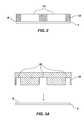
- FIG. 1is a top view of a carrier substrate according to the present invention having an array of image sensor chip attachment areas.
- FIG. 2is a side view of the carrier substrate of FIG. 1 having a layer of barrier material formed on its top surface.
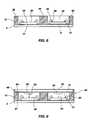
- FIGS. 3A through 3Care schematic sectional side views showing a first method for forming the layer of barrier material depicted in FIG. 2 by molding it onto the carrier substrate.
- FIG. 3Dis a top view of the carrier substrate depicted in FIG. 1 after the addition of the layer of barrier material.
- FIGS. 4A and 4Bare partial sectional side views showing a second method for forming the layer of barrier material depicted in FIG. 2 by depositing layers of a cure-hardened liquid onto the carrier substrate.
- FIGS. 5A and 5Bare sectional side views showing a third method for forming the layer of barrier material depicted in FIG. 2 by using stereolithography.
- FIGS. 6 and 7are perspective views showing a fourth method for forming the layer of barrier material depicted in FIG. 2 by attaching a preformed unitary frame to the carrier substrate.
- FIG. 8is a sectional side view showing image sensor chips mounted and wire bonded within chip cavities formed by the carrier substrate and the layer of barrier material.
- FIG. 9is a sectional side view showing a unitary transparent cover sealed to the assembly depicted in FIG. 8 .
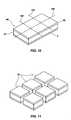
- FIG. 10is a perspective view of an image sensor array prior to singulation.
- FIG. 11is a perspective view of an individual image sensor package which has been separated from the image sensor array depicted in FIG. 10 .
- FIG. 12is a sectional side view of the image sensor package depicted in FIG. 11 , wherein castellated solder pads have been added to form a leadless chip carrier.
- FIG. 13is a side sectional view of the image sensor package depicted in FIG. 11 , wherein an array of discrete conductive elements has been added to form a ball grid array package.
- a carrier substrate 2shown in FIG. 1 , is provided with an array of image sensor chip attachment areas 4 formed on its top surface 6 .
- Broken section lines 100are shown running in mutually perpendicular horizontal and vertical directions on top surface 6 to indicate the boundary between adjacent image sensor chip attachment areas 4 .
- Carrier substrate 2may be a printed circuit board (PCB) having conductive traces 8 (see FIGS. 12 and 13 ) thereon, and may be formed using conventional PCB fabrication techniques.
- PCBprinted circuit board
- Carrier substrate 2may be constructed with common PCB materials such as a BT resin or FR-4 or FR-5 laminate in order to reduce cost, but other materials such as silicon, ceramics or plastics may be used as well.
- Each image sensor chip attachment area 4includes a chip adherence surface 9 bounded by a plurality of wire bonding locations 10 for wire bonding to conductive traces 8 , one of which is shown in broken lines in FIG. 1 , conductive traces 8 extending to locations for electrical connection of the completed image sensor package to higher-level packaging, such as a circuit board, for operation.
- the length, orientation and configuration of conductive traces 8may be as desired, depending on the I/O format used to connect the completed image sensor package, and so will not be discussed further at this juncture.
- a layer of barrier material 12 having apertures 14 therein coinciding with image sensor chip attachment areas 4is then formed on, or secured to, the carrier substrate top surface 6 , as illustrated in FIG. 2 .
- layer of barrier material 12is formed from a mold compound 16 which is molded directly onto top surface 6 .
- FIGS. 3A through 3CThis method is depicted in FIGS. 3A through 3C .
- a transfer molding tool or platen 18 including contiguous mold cavities 20is placed in sealing relationship against top surface 6 of carrier substrate 2 with mold cavities 20 positioned over the perimeter of carrier substrate 2 and over areas coinciding with, and preferably bisected by, section lines 100 defining boundaries between adjacent image sensor chip attachment areas 4 .
- FIG. 3Aa transfer molding tool or platen 18 including contiguous mold cavities 20 is placed in sealing relationship against top surface 6 of carrier substrate 2 with mold cavities 20 positioned over the perimeter of carrier substrate 2 and over areas coinciding with, and preferably bisected by, section lines 100 defining boundaries between adjacent image sensor chip attachment areas 4 .
- FIG. 3Bshows that a liquified or otherwise molten mold compound 16 , such as a thermoplastic, silicon-filled polymer, is rapidly transferred under pressure from a reservoir 22 into mold cavities 20 via a plurality of runners 24 , the general process of transfer molding being well known in the art.
- the mold compound 16then cures and hardens as it cools, and molding tool 18 is removed from the top surface 6 of carrier substrate 2 , leaving the structure as seen in FIG. 3C .
- the cured mold compound 16comprises a contiguous matrix of raised walls 26 that surround each image sensor chip attachment area 4 to define apertures 14 , leaving the portion of image sensor chip attachment areas 4 containing chip adherence surface 9 and wire bonding locations 10 exposed, creating an array of chip cavities 28 sized and configured for receiving image sensor chips 52 , which are described in further detail below.
- FIG. 3Dis a top view of carrier substrate 2 showing the arrangement of raised walls 26 surrounding chip attachment areas 4 .
- mold compound 16may be a thermoplastic polymer or other suitable encapsulant material as known in the art. Further, a filler material such as fine silicon particles may be incorporated within the mold compound to reduce cost, also as known in the art. It should also be understood that while the present invention is described in terms of transfer molding, other molding techniques such as injection molding or pot molding could be used with an appropriately formulated mold compound. Other suitable materials for mold compounds as known in the art include, without limitation, thermoset polymers and epoxy compounds.
- Another approach to forming a layer of barrier material 12 onto top surface 6includes disposing a flowable material on top surface 6 in one or more sequentially cured layers to build the contiguous matrix of raised walls 26 .
- a high-viscosity liquid or gel 30is dispensed from a nozzle 32 around the perimeter of carrier substrate 2 and along section lines 100 (not shown). The high-viscosity liquid or gel 30 is then cured to form a first hardened layer 34 .
- FIG. 4Ban additional layer of high-viscosity liquid or gel 30 is dispensed over first hardened layer 34 and cured to form second hardened layer 36 .
- Liquid or gel 30may comprise an activated epoxy or any other curable resin-type material that may be hardened by reaction of constituents thereof, application of heat thereto, or otherwise as known in the art.
- STLstereolithographic
- STLinvolves the formation of solid structures by selectively curing portions of volumes of a liquid polymer or resin material contained within a tank or reservoir. Depending on the liquid material composition, curing may he accomplished by exposure to irradiation with selected wavelengths of light or other electromagnetic radiation, for instance, when curing a material susceptible to initiation of cross-linking by exposure to ultraviolet (UV) radiation, such as through use of a UV laser beam.
- UVultraviolet
- FIGS. 5A and 5Billustrate this technique.
- carrier substrate 2is placed to a selected depth below the surface of a photocurable liquid 38 contained within a reservoir 40 .
- the use of a photocurable liquid 38is only exemplary, and liquid materials cured by other activating agents could also be used.
- a focused beam of lightsuch as a laser beam 42 is directed over the surface of photocurable liquid 38 in a pattern that coincides with the perimeter of carrier substrate 2 and section lines 100 between image sensor chip attachment areas 4 .
- FIG. 5Bshows that carrier substrate 2 may then be lowered another selected depth within reservoir 40 , and the beam of light 42 directed over the same pattern to form a second layer of cured material 46 on top of the first layer 44 .
- subsequent layersmay be added until the desired height for layer of barrier material 12 is reached.
- Complete and accelerated curing of the photocurable materialmay be effected by devoted temperatures after cross-linking is initiated.
- Suitable equipment for forming a barrier layer as describedis commercially available from 3D Systems, Inc. of Valencia, Calif.
- Suitable photocurable liquidswhich may be used with the 3D Systems, Inc. equipment is available from Ciba Specialty Chemicals Corporation.
- FIG. 6shows an exemplary preformed unitary frame 48 used for this purpose.
- Unitary frame 48may be preformed by one of the previously described molding techniques, or may be formed from a sheet of solid material such as a plastic, silicon or green ceramic by removal of selected portions thereof.
- the array of apertures 14may be directly molded into unitary frame 48 .
- apertures 14may be cut, stamped, milled or etched into a sheet of material, the process employed being dictated by the material selected.
- unitary frame 48may be secured to top surface 6 of carrier substrate 2 with an adhesive material 50 , as illustrated in FIG.
- Adhesive material 50may be in the form of an epoxy, a silicone, an acrylic or other liquid-type adhesive applied to top surface 6 and/or unitary frame 48 , or may comprise a double-sided adhesive-coated tape segment or film, such as a polyimide.
- a two-component resinmay be employed, with one component applied in an appropriate pattern to top surface 6 of carrier substrate 2 and the other to a surface of frame 48 to be placed in contact with top surface 6 to prevent premature component reaction and adhesion.
- an image sensor chip 52is mounted within each of the chip cavities 28 on chip adherence surface 9 .
- Image sensor chips 52are secured to chip adherence surface 9 with a layer of adhesive material 54 , as shown in FIG. 8 .
- the layer of adhesive material 54may be an epoxy, a silicone, an acrylic or other liquid-type adhesive, a two-component resin, or a double-sided adhesive-coated tape segment or film.
- adhesive material 54may comprise a conductive adhesive or bonding agent to ground or electrically bias the back side of image sensor chips 52 , in which instance a conductive or conductor-filled epoxy, a silver solder or a Z-axis anisotropic conductive adhesive may be employed. If a preformed frame 48 is used for layer of barrier material 12 and raised walls 26 , adhesive material 50 and the layer of adhesive material 54 may be applied to top surface 6 of carrier substrate 2 at the same time, in a single step, before preformed frame 48 is aligned with carrier substrate 2 and placed on top surface 6 .
- bond pads 56 on the active surface 58 of each image sensor chip 52are connected to wire bonding locations 10 on top surface 6 with gold or aluminum wire bonds 60 , as known in the art. It is contemplated that, if a preformed frame 48 is used for layer of barrier material 12 , image sensor chips 52 may be placed, wire bonds 60 formed, and then preformed frame 48 carrying adhesive on the surface thereof facing top surface 6 of carrier substrate 2 aligned and adhered to top surface 6 to provide enhanced clearance for a wire bonding capillary.
- Unitary transparent cover 62is configured to substantially conform to the configuration of carrier substrate 2 , so that it covers the entire array of chip cavities 28 and extends over the peripherally outer portions of the contiguous matrix of raised walls 26 . Stated another way, unitary transparent cover 62 is dimensioned substantially the same as carrier substrate 2 , such term including both slightly smaller and slightly larger dimensions. In FIG. 9 , unitary transparent cover 62 is aligned with carrier substrate 2 , placed on the top of the layer of barrier material 12 and continuously sealed in place along the tops of the matrix of raised walls 26 . Unitary transparent cover 62 may be formed of an at least partially optically transparent material such as borosilicate glass (BSG).
- BSGborosilicate glass
- unitary transparent cover 62may be formed to provide an optical function, for example, shaping its surface at locations corresponding to chip cavities 28 to act as focusing microlenses, as shown in broken lines 65 .
- a bead of epoxy, silicone gel or other liquid or gel adhesive 64may be applied to the tops of raised walls 26 of the layer of barrier material 12 , directly to unitary transparent cover 62 along selected lines, or both, prior to attachment.
- a two-component adhesive resinmay be employed, with one component applied to the tops of raised walls 26 and the other to unitary transparent cover 62 so that a cure will not commence until the two components are in contact.
- Other sealing mechanismssuch as the previously described double-sided adhesive-coated tape, may be used as well, as long as they provide a suitable hermetic bond.
- any adhesive usedbe of a type which does not outgas volatiles or other compounds when curing, so as not to compromise the properties of the image sensor chips 52 .
- a snap-cure epoxyas known in the art, may be suitable, as may an epoxy cured to a B-stage, or tacky state, prior to application of unitary transparent cover 62 .
- the layer of barrier material 12may be of a composition such that a thermal- or pressure-initiated bonding process may be used to adhere unitary transparent cover 62 directly to layer of barrier material 12 without the aid of an additional adhesive. As seen in FIG.
- a vertical gap 63exists between active surfaces 58 of image sensor chips 52 and unitary transparent cover 62 .
- active surface 58it is often a requirement that active surface 58 be free of contact from any covering material to prevent interference with sensing circuitry and unwanted refraction of light. Accordingly, when one of these high-end image sensor chips is packaged using the present invention, gap 63 will be left free of any filler material. Gap 63 also maintains unitary transparent cover 62 above the tops of wire bonds 60 . If an image sensor chip 52 not having the requirement of a material-free gap is used, a transparent encapsulant material 67 may be used to fill chip cavities 28 .
- Such transparent encapsulant material 67which is indicated by a broken lead line extending into chip cavity 28 in FIG. 9 , may also be used to provide a transitional index of refraction between the image sensor and the index of refraction of the unitary transparent cover 62 , if desired. This approach would also secure and protect wire bonds 60 , and the transparent encapsulant material 67 may also be used as the adhesive mechanism for securing unitary transparent cover 62 .
- Example materials for transparent encapsulant material 67may include clear epoxy, silicone, acrylic or other suitably transparent resin type materials.
- a raised lip 66may be formed around the perimeter of the layer of barrier material 12 , as shown in FIG. 9 .
- Raised lip 66may be formed integrally with, and at the same time as, forming the layer of barrier material 12 by any previously described technique.
- Unitary transparent cover 62may then be aligned with the layer of barrier material 12 by placement within raised lip 66 .
- FIG. 10is a perspective view of image sensor package array 68 , having the location of section lines 100 indicated above the top surface thereof.
- Carrier substrate 2 , the layer of barrier material 12 and unitary transparent cover 62are simultaneously cut along section lines 100 which run along the centers of raised walls 26 and divide image sensor package array 68 into individual image sensor packages 70 as shown in FIG. 11 .
- Thismay be accomplished, for example, by cutting or scribing (followed by snapping image sensor packages 70 apart along the scribe lines) with a conventional wafer saw.
- the individual image sensor packages 70may be singulated using a laser or other high energy beam.
- metallized pads or other contact interfaces for electrical communication of image sensor chip 52 through conductive traces 8are required.
- a plurality of castellated solder pads 72 in respective communication with different traces 8may be formed by techniques known in the art around the perimeter of a singulated image sensor package 70 to form a leadless chip-carrier (LCC) image sensor package.
- LCCleadless chip-carrier
- discrete conductive elements 74such as tin/lead solder balls, gold bumps or conductive or conductor-filled epoxy bumps, columns or pillars may be formed on or attached to the lower ends of vias 76 extending from conductive traces 8 in an array pattern on the bottom of singulated image sensor package 70 to form a ball-grid array (BGA)-type image sensor package, as illustrated by FIG. 13 .
- a redistribution layer (RDL) of conductive traces 78may also be applied to or formed on the bottom surface 80 of carrier substrate 2 in communication with the lower ends of selected vias 76 to configure a suitable pad array for formation or disposition of discrete conductive elements 74 thereon.
- discrete conductive elements 74be attached to image sensor package array 68 prior to its singulation into individual image sensor packages 70 . This would be advantageous as discrete conductive elements 74 may thus be formed on or applied to all of the image sensor packages 70 of a given image sensor package array in a single step.
- unitary transparent cover 62 and barrier material 12would then be secured to the top surface 6 of carrier substrate 2 after attachment and electrical connection of image sensor chips 52 to image sensor chip attachment areas 4 .
- securing and hermetic sealing of barrier material 12 to carrier substrate 2may be accomplished with a bead of epoxy, silicone or other liquid or gel adhesive, double-sided adhesive-coated tape or thermal or pressure initiated bonding.
Landscapes
- Engineering & Computer Science (AREA)
- Computer Hardware Design (AREA)
- Microelectronics & Electronic Packaging (AREA)
- Power Engineering (AREA)
- Solid State Image Pick-Up Elements (AREA)
Abstract
Description
- This application is a divisional of application Ser. No. 10/228,411, filed Aug. 26, 2002, pending.
- 1. Field of the Invention
- The present invention relates to packaging of optically interactive electronic devices. More particularly, the present invention relates to a package for a solid-state image sensor and methods for simultaneously assembling a plurality of such packages.
- 2. State of the Art
- Solid-state image sensors, for example, charge coupled device (CCD) or complementary metal-oxide semiconductor (CMOS) chips, are increasingly in demand for incorporation into electronic devices. They may be used for a variety of applications including consumer electronics like digital cameras, cellular telephones and hand-held scanners. Conventionally, these image sensor chips have been packaged within a discrete housing for protection from environmental stresses and to provide electrical communication with other components of the larger electronic device into which they are incorporated. The typical housing is a unitary ceramic or plastic shell having a cavity into which an image sensor chip is mounted. The chip is wire bonded to conductive elements within the cavity, and a window or at least partially optically transparent lid covers the cavity to allow light or other forms of electromagnetic radiation to pass through to sensing circuitry on the active surface of the chip. The transparent lid may also be formed to provide an optical function such as focusing the light or other radiation and/or filtering selected wavelengths thereof. The materials and structure involved with this packaging technique require a fabrication process that can be time consuming, costly and consist of several precision assembly steps. Due to the competitive nature of today's semiconductor industry, even a small reduction in packaging cost would be of great benefit, especially when considered in terms of the high volume of components being manufactured to meet growing demands.
- In response to large-scale production requirements, various attempts have been made to simplify the construction of image sensor packaging. U.S. Pat. No. 6,351,027 to Giboney et al. and U.S. Pat. No. 6,285,064 to Foster, for instance, disclose wafer-level packaging formed by laying a solid sidewall piece or an adhesive matrix over a wafer having an array of sensor devices and covering it with a transparent top piece. The wafer is then singulated to create discrete chip-scale packages. While this approach reduces material costs and assembly steps, it does not completely protect the semiconductor chips from the environment and requires attaching material directly to the wafer surface, which could damage the sensor devices. U.S. Pat. No. 6,266,197 to Glenn et al. discloses a method for forming image sensor packages wherein an array of image sensors is wire bonded to a carrier substrate, and a molded window array is placed over the array of image sensors. The substrate and attached molded window array are then singulated to form a plurality of individual image sensor packages. The molded window array of Glenn et al., however, still suffers from the fact that individual transparent windows must be formed within or later attached to the molded array, requiring additional assembly and alignment steps during fabrication. U.S. Pat. No. 5,811,799 to Wu discloses an image sensor package formed by attaching a plurality of preformed or glue walls to an array of printed wiring frames having image sensors thereon and sealing the walls with transparent material. The printed wiring frames are then diced to form discrete packages. Once again, this arrangement may require the attachment or formation of multiple components during fabrication, and the disclosed printed wiring frames have a conductive via output arrangement that may not be suitable for certain high I/O image sensor chips.
- As is evident from the foregoing description of the state of the art, what is needed is a simplified method for forming an image sensor package that is conducive to mass production while still offering suitable and robust protection for an image sensor chip.
- In accordance with the present invention, a plurality of packages for image sensors and other optically interactive electronic devices are simultaneously fabricated to minimize assembly steps and reduce the cost associated with each individual package. A carrier substrate is provided with an array of image sensor chip or other optically interactive electronic device attachment areas. A layer of barrier material having apertures coinciding with the chip or device attachment areas is formed on, or secured to, the substrate surface to create an array of cavities, each sized and configured for containing an image sensor chip or other optically interactive electronic device. An image sensor chip or other optically interactive electronic device is mounted within each cavity and wire bonded to conductive traces on the carrier substrate. A unitary, at least partially optically transparent cover is then sealed in place over the unitary layer of barrier material. Next, the assembly is cut or otherwise divided along lines running between adjacent cavities to form a plurality of individual packages. If required, the packages may then proceed through additional fabrication steps such as solder ball attachment or castellated pad formation, or these steps may be completed prior to dividing the assembly into individual packages.
- While described primarily in terms of an image sensor package, it is to be understood that the present invention may be used for packaging various other optically interactive electronic devices which require a window for access to a device surface. The term “optically interactive” as used herein is meant to encompass devices sensitive to various wavelengths of light or other forms of radiation, including, but not limited to, CCD and CMOS image sensors, EPROM's, and photodiodes, as well as light-emitting devices including semiconductor lasers and light-emitting diodes.
- Other and further features and advantages will be apparent from the following detailed description of the present invention when read in conjunction with the accompanying drawings. It should be understood that the described embodiments are provided for illustrative and exemplary purposes only, and that variations to, and combinations of, the several elements and features thereof are contemplated as being within the scope of the invention.
- In the drawings, which illustrate what is currently considered to be the best mode for carrying out the invention:
FIG. 1 is a top view of a carrier substrate according to the present invention having an array of image sensor chip attachment areas.FIG. 2 is a side view of the carrier substrate ofFIG. 1 having a layer of barrier material formed on its top surface.FIGS. 3A through 3C are schematic sectional side views showing a first method for forming the layer of barrier material depicted inFIG. 2 by molding it onto the carrier substrate.FIG. 3D is a top view of the carrier substrate depicted inFIG. 1 after the addition of the layer of barrier material.FIGS. 4A and 4B are partial sectional side views showing a second method for forming the layer of barrier material depicted inFIG. 2 by depositing layers of a cure-hardened liquid onto the carrier substrate.FIGS. 5A and 5B are sectional side views showing a third method for forming the layer of barrier material depicted inFIG. 2 by using stereolithography.FIGS. 6 and 7 are perspective views showing a fourth method for forming the layer of barrier material depicted inFIG. 2 by attaching a preformed unitary frame to the carrier substrate.FIG. 8 is a sectional side view showing image sensor chips mounted and wire bonded within chip cavities formed by the carrier substrate and the layer of barrier material.FIG. 9 is a sectional side view showing a unitary transparent cover sealed to the assembly depicted inFIG. 8 .FIG. 10 is a perspective view of an image sensor array prior to singulation.FIG. 11 is a perspective view of an individual image sensor package which has been separated from the image sensor array depicted inFIG. 10 .FIG. 12 is a sectional side view of the image sensor package depicted inFIG. 11 , wherein castellated solder pads have been added to form a leadless chip carrier.FIG. 13 is a side sectional view of the image sensor package depicted inFIG. 11 , wherein an array of discrete conductive elements has been added to form a ball grid array package.- Referring in general to the accompanying drawings, various aspects of the present invention are illustrated to show exemplary image sensor package structures and methods for assembly of a package for housing an image sensor chip. Common elements of the illustrated embodiments are designated with like reference numerals. It should be understood that the figures presented are not meant to be illustrative of actual views of any particular portion of a particular image sensor package structure, but are merely idealized schematic representations which are employed to more clearly and fully depict the invention. It should further be understood that while depicted in terms of an image sensor, the package embodiments and methods presented herein would work equally well for housing other types of optically interactive electronic devices as described above.
- Turning to
FIGS. 1 through 13 , methods for simultaneously assembling a plurality of image sensor packages according to the present invention are illustrated. Acarrier substrate 2, shown inFIG. 1 , is provided with an array of image sensorchip attachment areas 4 formed on itstop surface 6. Broken section lines100 are shown running in mutually perpendicular horizontal and vertical directions ontop surface 6 to indicate the boundary between adjacent image sensorchip attachment areas 4.Carrier substrate 2 may be a printed circuit board (PCB) having conductive traces8 (seeFIGS. 12 and 13 ) thereon, and may be formed using conventional PCB fabrication techniques.Carrier substrate 2 may be constructed with common PCB materials such as a BT resin or FR-4 or FR-5 laminate in order to reduce cost, but other materials such as silicon, ceramics or plastics may be used as well. Each image sensorchip attachment area 4 includes achip adherence surface 9 bounded by a plurality ofwire bonding locations 10 for wire bonding toconductive traces 8, one of which is shown in broken lines inFIG. 1 ,conductive traces 8 extending to locations for electrical connection of the completed image sensor package to higher-level packaging, such as a circuit board, for operation. The length, orientation and configuration ofconductive traces 8 may be as desired, depending on the I/O format used to connect the completed image sensor package, and so will not be discussed further at this juncture. - A layer of
barrier material 12 havingapertures 14 therein coinciding with image sensorchip attachment areas 4 is then formed on, or secured to, the carriersubstrate top surface 6, as illustrated inFIG. 2 . In a currently preferred embodiment of the present invention, layer ofbarrier material 12 is formed from amold compound 16 which is molded directly ontotop surface 6. This method is depicted inFIGS. 3A through 3C . As shown inFIG. 3A , a transfer molding tool orplaten 18 includingcontiguous mold cavities 20 is placed in sealing relationship againsttop surface 6 ofcarrier substrate 2 withmold cavities 20 positioned over the perimeter ofcarrier substrate 2 and over areas coinciding with, and preferably bisected by,section lines 100 defining boundaries between adjacent image sensorchip attachment areas 4.FIG. 3B shows that a liquified or otherwise moltenmold compound 16, such as a thermoplastic, silicon-filled polymer, is rapidly transferred under pressure from areservoir 22 intomold cavities 20 via a plurality ofrunners 24, the general process of transfer molding being well known in the art. Themold compound 16 then cures and hardens as it cools, andmolding tool 18 is removed from thetop surface 6 ofcarrier substrate 2, leaving the structure as seen inFIG. 3C . The curedmold compound 16 comprises a contiguous matrix of raisedwalls 26 that surround each image sensorchip attachment area 4 to defineapertures 14, leaving the portion of image sensorchip attachment areas 4 containingchip adherence surface 9 andwire bonding locations 10 exposed, creating an array ofchip cavities 28 sized and configured for receiving image sensor chips52, which are described in further detail below.FIG. 3D is a top view ofcarrier substrate 2 showing the arrangement of raisedwalls 26 surroundingchip attachment areas 4. - As noted above,
mold compound 16 may be a thermoplastic polymer or other suitable encapsulant material as known in the art. Further, a filler material such as fine silicon particles may be incorporated within the mold compound to reduce cost, also as known in the art. It should also be understood that while the present invention is described in terms of transfer molding, other molding techniques such as injection molding or pot molding could be used with an appropriately formulated mold compound. Other suitable materials for mold compounds as known in the art include, without limitation, thermoset polymers and epoxy compounds. - Another approach to forming a layer of
barrier material 12 ontotop surface 6 includes disposing a flowable material ontop surface 6 in one or more sequentially cured layers to build the contiguous matrix of raisedwalls 26. In one exemplary embodiment of this method shown inFIG. 4A , a high-viscosity liquid orgel 30 is dispensed from anozzle 32 around the perimeter ofcarrier substrate 2 and along section lines100 (not shown). The high-viscosity liquid orgel 30 is then cured to form a firsthardened layer 34. InFIG. 4B , an additional layer of high-viscosity liquid orgel 30 is dispensed over firsthardened layer 34 and cured to form secondhardened layer 36. Subsequent layers of liquid orgel 30 may be added, as desired, until the desired height for layer ofbarrier material 12 is reached. Liquid orgel 30 may comprise an activated epoxy or any other curable resin-type material that may be hardened by reaction of constituents thereof, application of heat thereto, or otherwise as known in the art. - Another exemplary embodiment of this layering approach exists in using a stereolithographic (STL) deposition process to form the contiguous matrix of raised
walls 26 ontop surface 6. As defined in the art, STL involves the formation of solid structures by selectively curing portions of volumes of a liquid polymer or resin material contained within a tank or reservoir. Depending on the liquid material composition, curing may he accomplished by exposure to irradiation with selected wavelengths of light or other electromagnetic radiation, for instance, when curing a material susceptible to initiation of cross-linking by exposure to ultraviolet (UV) radiation, such as through use of a UV laser beam. By curing one or more successive layers of the liquid material, intricate solid structures of almost any shape may be formed. It is also possible to add elements to an existing structure using STL, as would be the case with the present invention.FIGS. 5A and 5B illustrate this technique. InFIG. 5A ,carrier substrate 2 is placed to a selected depth below the surface of a photocurable liquid38 contained within areservoir 40. The use of a photocurable liquid38 is only exemplary, and liquid materials cured by other activating agents could also be used. A focused beam of light such as alaser beam 42 is directed over the surface of photocurable liquid38 in a pattern that coincides with the perimeter ofcarrier substrate 2 andsection lines 100 between image sensorchip attachment areas 4. The portions of the photocurable liquid38 exposed tolaser beam 42 cures to at least a semisolid state, forming a first layer of curedmaterial 44 ontop surface 6.FIG. 5B shows thatcarrier substrate 2 may then be lowered another selected depth withinreservoir 40, and the beam of light42 directed over the same pattern to form a second layer of curedmaterial 46 on top of thefirst layer 44. As with the previous dispensing embodiment, subsequent layers may be added until the desired height for layer ofbarrier material 12 is reached. Complete and accelerated curing of the photocurable material may be effected by devoted temperatures after cross-linking is initiated. Suitable equipment for forming a barrier layer as described is commercially available from 3D Systems, Inc. of Valencia, Calif. Suitable photocurable liquids which may be used with the 3D Systems, Inc. equipment is available from Ciba Specialty Chemicals Corporation. - In certain situations, it may be desirable to preform the layer of
barrier material 12 defined by raisedwalls 26 and then secure it tocarrier substrate 2.FIG. 6 shows an exemplary preformedunitary frame 48 used for this purpose.Unitary frame 48 may be preformed by one of the previously described molding techniques, or may be formed from a sheet of solid material such as a plastic, silicon or green ceramic by removal of selected portions thereof. In the case of molding, the array ofapertures 14 may be directly molded intounitary frame 48. When formed from a solid material,apertures 14 may be cut, stamped, milled or etched into a sheet of material, the process employed being dictated by the material selected. Once completed,unitary frame 48 may be secured totop surface 6 ofcarrier substrate 2 with anadhesive material 50, as illustrated inFIG. 7 .Adhesive material 50 may be in the form of an epoxy, a silicone, an acrylic or other liquid-type adhesive applied totop surface 6 and/orunitary frame 48, or may comprise a double-sided adhesive-coated tape segment or film, such as a polyimide. Alternatively, a two-component resin may be employed, with one component applied in an appropriate pattern totop surface 6 ofcarrier substrate 2 and the other to a surface offrame 48 to be placed in contact withtop surface 6 to prevent premature component reaction and adhesion. - After formation or attachment of the layer of
barrier material 12 ontop surface 6, animage sensor chip 52 is mounted within each of thechip cavities 28 onchip adherence surface 9. Image sensor chips52 are secured to chipadherence surface 9 with a layer ofadhesive material 54, as shown inFIG. 8 . As withadhesive material 50, the layer ofadhesive material 54 may be an epoxy, a silicone, an acrylic or other liquid-type adhesive, a two-component resin, or a double-sided adhesive-coated tape segment or film. If required or desired,adhesive material 54 may comprise a conductive adhesive or bonding agent to ground or electrically bias the back side of image sensor chips52, in which instance a conductive or conductor-filled epoxy, a silver solder or a Z-axis anisotropic conductive adhesive may be employed. If a preformedframe 48 is used for layer ofbarrier material 12 and raisedwalls 26,adhesive material 50 and the layer ofadhesive material 54 may be applied totop surface 6 ofcarrier substrate 2 at the same time, in a single step, before preformedframe 48 is aligned withcarrier substrate 2 and placed ontop surface 6. Onceimage sensor chips 52 are in place,bond pads 56 on theactive surface 58 of eachimage sensor chip 52 are connected to wirebonding locations 10 ontop surface 6 with gold oraluminum wire bonds 60, as known in the art. It is contemplated that, if a preformedframe 48 is used for layer ofbarrier material 12, image sensor chips52 may be placed,wire bonds 60 formed, and then preformedframe 48 carrying adhesive on the surface thereof facingtop surface 6 ofcarrier substrate 2 aligned and adhered totop surface 6 to provide enhanced clearance for a wire bonding capillary. - The resulting assembly is now ready to receive a unitary
transparent cover 62. Unitarytransparent cover 62 is configured to substantially conform to the configuration ofcarrier substrate 2, so that it covers the entire array ofchip cavities 28 and extends over the peripherally outer portions of the contiguous matrix of raisedwalls 26. Stated another way, unitarytransparent cover 62 is dimensioned substantially the same ascarrier substrate 2, such term including both slightly smaller and slightly larger dimensions. InFIG. 9 , unitarytransparent cover 62 is aligned withcarrier substrate 2, placed on the top of the layer ofbarrier material 12 and continuously sealed in place along the tops of the matrix of raisedwalls 26. Unitarytransparent cover 62 may be formed of an at least partially optically transparent material such as borosilicate glass (BSG). Of course, other types of glass, quartz or even plastic which allow the passage of a desired range of wavelengths of light or other forms of electromagnetic radiation may also be used. Furthermore, unitarytransparent cover 62 may be formed to provide an optical function, for example, shaping its surface at locations corresponding to chipcavities 28 to act as focusing microlenses, as shown inbroken lines 65. - To secure unitary
transparent cover 62 in place along the tops of raisedwalls 26 and hermetically seal theimage sensor chips 52 within eachrespective chip cavity 28, a bead of epoxy, silicone gel or other liquid or gel adhesive64 may be applied to the tops of raisedwalls 26 of the layer ofbarrier material 12, directly to unitarytransparent cover 62 along selected lines, or both, prior to attachment. If desired, a two-component adhesive resin may be employed, with one component applied to the tops of raisedwalls 26 and the other to unitarytransparent cover 62 so that a cure will not commence until the two components are in contact. Other sealing mechanisms, such as the previously described double-sided adhesive-coated tape, may be used as well, as long as they provide a suitable hermetic bond. It is desirable, so that the optical capabilities ofimage chip sensors 52 are not compromised, that any adhesive used be of a type which does not outgas volatiles or other compounds when curing, so as not to compromise the properties of the image sensor chips52. A snap-cure epoxy, as known in the art, may be suitable, as may an epoxy cured to a B-stage, or tacky state, prior to application of unitarytransparent cover 62. In some instances, the layer ofbarrier material 12 may be of a composition such that a thermal- or pressure-initiated bonding process may be used to adhere unitarytransparent cover 62 directly to layer ofbarrier material 12 without the aid of an additional adhesive. As seen inFIG. 9 , avertical gap 63 exists betweenactive surfaces 58 ofimage sensor chips 52 and unitarytransparent cover 62. For high-end image sensor chips52, it is often a requirement thatactive surface 58 be free of contact from any covering material to prevent interference with sensing circuitry and unwanted refraction of light. Accordingly, when one of these high-end image sensor chips is packaged using the present invention,gap 63 will be left free of any filler material.Gap 63 also maintains unitarytransparent cover 62 above the tops of wire bonds60. If animage sensor chip 52 not having the requirement of a material-free gap is used, atransparent encapsulant material 67 may be used to fillchip cavities 28. Suchtransparent encapsulant material 67, which is indicated by a broken lead line extending intochip cavity 28 inFIG. 9 , may also be used to provide a transitional index of refraction between the image sensor and the index of refraction of the unitarytransparent cover 62, if desired. This approach would also secure and protectwire bonds 60, and thetransparent encapsulant material 67 may also be used as the adhesive mechanism for securing unitarytransparent cover 62. Example materials fortransparent encapsulant material 67 may include clear epoxy, silicone, acrylic or other suitably transparent resin type materials. - In order to promote proper alignment of unitary
transparent cover 62, a raisedlip 66 may be formed around the perimeter of the layer ofbarrier material 12, as shown inFIG. 9 . Raisedlip 66 may be formed integrally with, and at the same time as, forming the layer ofbarrier material 12 by any previously described technique. Unitarytransparent cover 62 may then be aligned with the layer ofbarrier material 12 by placement within raisedlip 66. - Once unitary
transparent cover 62 is sealed in place, the assembly essentially comprises an imagesensor package array 68. Imagesensor package array 68 may now be cut or otherwise singulated to separate out individual image sensor packages.FIGS. 10 and 11 illustrate this process.FIG. 10 is a perspective view of imagesensor package array 68, having the location ofsection lines 100 indicated above the top surface thereof.Carrier substrate 2, the layer ofbarrier material 12 and unitarytransparent cover 62 are simultaneously cut alongsection lines 100 which run along the centers of raisedwalls 26 and divide imagesensor package array 68 into individual image sensor packages70 as shown inFIG. 11 . This may be accomplished, for example, by cutting or scribing (followed by snapping image sensor packages70 apart along the scribe lines) with a conventional wafer saw. Alternatively, the individual image sensor packages70 may be singulated using a laser or other high energy beam. - For attachment of an
image sensor package 70 to a higher-level packaging component such as an assembly substrate for communication with other components of an electronic device, metallized pads or other contact interfaces for electrical communication ofimage sensor chip 52 throughconductive traces 8 are required. In one exemplary embodiment of the present invention shown inFIG. 12 , a plurality ofcastellated solder pads 72 in respective communication withdifferent traces 8 may be formed by techniques known in the art around the perimeter of a singulatedimage sensor package 70 to form a leadless chip-carrier (LCC) image sensor package. In another exemplary embodiment shown inFIG. 13 , discreteconductive elements 74 such as tin/lead solder balls, gold bumps or conductive or conductor-filled epoxy bumps, columns or pillars may be formed on or attached to the lower ends ofvias 76 extending fromconductive traces 8 in an array pattern on the bottom of singulatedimage sensor package 70 to form a ball-grid array (BGA)-type image sensor package, as illustrated byFIG. 13 . A redistribution layer (RDL) ofconductive traces 78 may also be applied to or formed on thebottom surface 80 ofcarrier substrate 2 in communication with the lower ends of selected vias76 to configure a suitable pad array for formation or disposition of discreteconductive elements 74 thereon. It is also contemplated, and currently preferred with a BGA-type arrangement, that discreteconductive elements 74 be attached to imagesensor package array 68 prior to its singulation into individual image sensor packages70. This would be advantageous as discreteconductive elements 74 may thus be formed on or applied to all of the image sensor packages70 of a given image sensor package array in a single step. - All of the above-illustrated embodiments and variations thereof of the present invention provide image sensor packages that are simultaneously fabricated to minimize assembly steps and reduce the cost associated with each individual package. Although the present invention has been depicted and described with respect to the illustrated embodiments, various additions, deletions and modifications are contemplated within its scope. For instance, if so desired, it is also contemplated that the layer of
barrier material 12 may initially be formed on, or secured to, unitarytransparent cover 62 rather thancarrier substrate 2. Barrier material would be similarly formed on unitarytransparent cover 62 using one of the above described molding, deposited layering, or preform attach methods described above. The combination of unitarytransparent cover 62 andbarrier material 12 would then be secured to thetop surface 6 ofcarrier substrate 2 after attachment and electrical connection ofimage sensor chips 52 to image sensorchip attachment areas 4. In the same manner, securing and hermetic sealing ofbarrier material 12 tocarrier substrate 2 may be accomplished with a bead of epoxy, silicone or other liquid or gel adhesive, double-sided adhesive-coated tape or thermal or pressure initiated bonding. - Furthermore, as previously discussed, the present invention would be suitable for packaging various other types of optically interactive electronic devices. The scope of the invention is, therefore, indicated by the appended claims rather than the foregoing description. Further, all changes which may fall within the meaning and range of equivalency of the claims and elements and features thereof are to be embraced within their scope.
Claims (25)
Priority Applications (1)
| Application Number | Priority Date | Filing Date | Title |
|---|---|---|---|
| US11/103,019US7541658B2 (en) | 2002-08-26 | 2005-04-11 | Optically interactive device package array |
Applications Claiming Priority (2)
| Application Number | Priority Date | Filing Date | Title |
|---|---|---|---|
| US10/228,411US20040038442A1 (en) | 2002-08-26 | 2002-08-26 | Optically interactive device packages and methods of assembly |
| US11/103,019US7541658B2 (en) | 2002-08-26 | 2005-04-11 | Optically interactive device package array |
Related Parent Applications (1)
| Application Number | Title | Priority Date | Filing Date |
|---|---|---|---|
| US10/228,411DivisionUS20040038442A1 (en) | 2002-08-26 | 2002-08-26 | Optically interactive device packages and methods of assembly |
Publications (2)
| Publication Number | Publication Date |
|---|---|
| US20050173811A1true US20050173811A1 (en) | 2005-08-11 |
| US7541658B2 US7541658B2 (en) | 2009-06-02 |
Family
ID=31887611
Family Applications (2)
| Application Number | Title | Priority Date | Filing Date |
|---|---|---|---|
| US10/228,411AbandonedUS20040038442A1 (en) | 2002-08-26 | 2002-08-26 | Optically interactive device packages and methods of assembly |
| US11/103,019Expired - LifetimeUS7541658B2 (en) | 2002-08-26 | 2005-04-11 | Optically interactive device package array |
Family Applications Before (1)
| Application Number | Title | Priority Date | Filing Date |
|---|---|---|---|
| US10/228,411AbandonedUS20040038442A1 (en) | 2002-08-26 | 2002-08-26 | Optically interactive device packages and methods of assembly |
Country Status (1)
| Country | Link |
|---|---|
| US (2) | US20040038442A1 (en) |
Cited By (18)
| Publication number | Priority date | Publication date | Assignee | Title |
|---|---|---|---|---|
| US20040266063A1 (en)* | 2003-06-25 | 2004-12-30 | Montgomery Stephen W. | Apparatus and method for manufacturing thermal interface device having aligned carbon nanotubes |
| US20080020511A1 (en)* | 2006-07-19 | 2008-01-24 | Advanced Chip Engineering Technology Inc. | Structure of image sensor module and a method for manufacturing of wafer level package |
| US20080061300A1 (en)* | 2006-09-12 | 2008-03-13 | Yi-Shung Chaug | Flexible backplane and methods for its manufacture |
| US20080136012A1 (en)* | 2006-12-08 | 2008-06-12 | Advanced Chip Engineering Technology Inc. | Imagine sensor package and forming method of the same |
| US20080185610A1 (en)* | 2007-02-02 | 2008-08-07 | Kushimatsu Yuichiro | Resin-sealed semiconductor light receiving element, manufacturing method thereof and electronic device using the same |
| US20090115049A1 (en)* | 2007-11-06 | 2009-05-07 | Shinko Electric Industries Co., Ltd. | Semiconductor package |
| US20090321863A1 (en)* | 2008-06-25 | 2009-12-31 | Micron Technology, Inc. | Method and apparatus providing an imager module with a permanent carrier |
| US20110006412A1 (en)* | 2009-07-07 | 2011-01-13 | Hynix Semiconductor Inc. | Semiconductor chip package and method for manufacturing thereof and stack package using the same |
| US20110108870A1 (en)* | 2008-05-28 | 2011-05-12 | Osram Opto Semiconductors Gmbh | Optoelectronic semiconductor component and printed circuit board |
| US20110228390A1 (en)* | 2010-03-22 | 2011-09-22 | Chia-Sheng Lin | Optical cover plate with improved solder mask dam on galss for image sensor package and fabrication method thereof |
| US20120178213A1 (en)* | 2008-12-16 | 2012-07-12 | Stmicroelectronics Asia Pacific Pte Ltd (Singapore) | Chip scale package structure with can attachment |
| US20130327931A1 (en)* | 2012-06-06 | 2013-12-12 | Pixart Imaging Incorporation | Package structure of optical apparatus |
| CN107369722A (en)* | 2017-06-27 | 2017-11-21 | 上海集成电路研发中心有限公司 | A kind of sensor-packaging structure and preparation method thereof |
| US10319767B2 (en)* | 2016-05-19 | 2019-06-11 | Canon Kabushiki Kaisha | Electronic component including an optical member fixed with adhesive |
| US20190256349A1 (en)* | 2018-02-20 | 2019-08-22 | Denso Corporation | Physical quantity sensor and semiconductor device |
| TWI691041B (en)* | 2019-01-29 | 2020-04-11 | 矽品精密工業股份有限公司 | Electronic package and package substrate thereof and method for manufacturing same |
| US20220041436A1 (en)* | 2019-01-31 | 2022-02-10 | Robert Bosch Gmbh | Method for producing a plurality of sensor devices, and sensor device |
| US11302658B2 (en)* | 2018-08-20 | 2022-04-12 | Sj Semiconductor(Jiangyin) Corporation | Fan-out antenna package structure and packaging method |
Families Citing this family (102)
| Publication number | Priority date | Publication date | Assignee | Title |
|---|---|---|---|---|
| US6617175B1 (en)* | 2002-05-08 | 2003-09-09 | Advanced Technology Materials, Inc. | Infrared thermopile detector system for semiconductor process monitoring and control |
| US7129519B2 (en)* | 2002-05-08 | 2006-10-31 | Advanced Technology Materials, Inc. | Monitoring system comprising infrared thermopile detector |
| US6906403B2 (en)* | 2002-06-04 | 2005-06-14 | Micron Technology, Inc. | Sealed electronic device packages with transparent coverings |
| US6964881B2 (en)* | 2002-08-27 | 2005-11-15 | Micron Technology, Inc. | Multi-chip wafer level system packages and methods of forming same |
| US7274094B2 (en)* | 2002-08-28 | 2007-09-25 | Micron Technology, Inc. | Leadless packaging for image sensor devices |
| ITMI20022467A1 (en)* | 2002-11-20 | 2004-05-21 | St Microelectronics Srl | PROCESS FOR REALIZING A BYTE SELECTION TRANSISTOR FOR |
| US7176044B2 (en)* | 2002-11-25 | 2007-02-13 | Henkel Corporation | B-stageable die attach adhesives |
| US6930377B1 (en)* | 2002-12-04 | 2005-08-16 | National Semiconductor Corporation | Using adhesive materials as insulation coatings for leadless lead frame semiconductor packages |
| KR100548554B1 (en)* | 2003-03-04 | 2006-02-02 | 주식회사 하이닉스반도체 | Test Vehicle Ball Grid Array Package |
| WO2004088415A2 (en)* | 2003-03-28 | 2004-10-14 | Advanced Technology Materials Inc. | Photometrically modulated delivery of reagents |
| US7063097B2 (en)* | 2003-03-28 | 2006-06-20 | Advanced Technology Materials, Inc. | In-situ gas blending and dilution system for delivery of dilute gas at a predetermined concentration |
| US7365442B2 (en)* | 2003-03-31 | 2008-04-29 | Osram Opto Semiconductors Gmbh | Encapsulation of thin-film electronic devices |
| JP3898666B2 (en)* | 2003-04-28 | 2007-03-28 | 松下電器産業株式会社 | Solid-state imaging device and manufacturing method thereof |
| JP4106003B2 (en)* | 2003-09-03 | 2008-06-25 | 松下電器産業株式会社 | Method for manufacturing solid-state imaging device |
| US6953891B2 (en) | 2003-09-16 | 2005-10-11 | Micron Technology, Inc. | Moisture-resistant electronic device package and methods of assembly |
| US6934065B2 (en)* | 2003-09-18 | 2005-08-23 | Micron Technology, Inc. | Microelectronic devices and methods for packaging microelectronic devices |
| US7915085B2 (en) | 2003-09-18 | 2011-03-29 | Cree, Inc. | Molded chip fabrication method |
| US20050242341A1 (en)* | 2003-10-09 | 2005-11-03 | Knudson Christopher T | Apparatus and method for supporting a flexible substrate during processing |
| US7583862B2 (en)* | 2003-11-26 | 2009-09-01 | Aptina Imaging Corporation | Packaged microelectronic imagers and methods of packaging microelectronic imagers |
| US7253397B2 (en)* | 2004-02-23 | 2007-08-07 | Micron Technology, Inc. | Packaged microelectronic imagers and methods of packaging microelectronic imagers |
| TWI284398B (en)* | 2004-03-26 | 2007-07-21 | Xintec Inc | Chip package structure and its wafer level package method |
| US8092734B2 (en)* | 2004-05-13 | 2012-01-10 | Aptina Imaging Corporation | Covers for microelectronic imagers and methods for wafer-level packaging of microelectronics imagers |
| US7253957B2 (en)* | 2004-05-13 | 2007-08-07 | Micron Technology, Inc. | Integrated optics units and methods of manufacturing integrated optics units for use with microelectronic imagers |
| US20050275750A1 (en) | 2004-06-09 | 2005-12-15 | Salman Akram | Wafer-level packaged microelectronic imagers and processes for wafer-level packaging |
| JP5252770B2 (en)* | 2004-06-10 | 2013-07-31 | 三星電子株式会社 | Image sensor package assembly method |
| US7498647B2 (en) | 2004-06-10 | 2009-03-03 | Micron Technology, Inc. | Packaged microelectronic imagers and methods of packaging microelectronic imagers |
| US7199439B2 (en)* | 2004-06-14 | 2007-04-03 | Micron Technology, Inc. | Microelectronic imagers and methods of packaging microelectronic imagers |
| US7262405B2 (en)* | 2004-06-14 | 2007-08-28 | Micron Technology, Inc. | Prefabricated housings for microelectronic imagers |
| JP3801601B2 (en)* | 2004-06-15 | 2006-07-26 | シャープ株式会社 | Manufacturing method of semiconductor wafer provided with lid and manufacturing method of semiconductor device |
| US7232754B2 (en)* | 2004-06-29 | 2007-06-19 | Micron Technology, Inc. | Microelectronic devices and methods for forming interconnects in microelectronic devices |
| US7294897B2 (en)* | 2004-06-29 | 2007-11-13 | Micron Technology, Inc. | Packaged microelectronic imagers and methods of packaging microelectronic imagers |
| TWI236111B (en)* | 2004-06-30 | 2005-07-11 | Ind Tech Res Inst | Apparatus and method for wafer level packaging |
| US7416913B2 (en)* | 2004-07-16 | 2008-08-26 | Micron Technology, Inc. | Methods of manufacturing microelectronic imaging units with discrete standoffs |
| US7189954B2 (en)* | 2004-07-19 | 2007-03-13 | Micron Technology, Inc. | Microelectronic imagers with optical devices and methods of manufacturing such microelectronic imagers |
| US7402453B2 (en)* | 2004-07-28 | 2008-07-22 | Micron Technology, Inc. | Microelectronic imaging units and methods of manufacturing microelectronic imaging units |
| US20060023107A1 (en)* | 2004-08-02 | 2006-02-02 | Bolken Todd O | Microelectronic imagers with optics supports having threadless interfaces and methods for manufacturing such microelectronic imagers |
| US7364934B2 (en)* | 2004-08-10 | 2008-04-29 | Micron Technology, Inc. | Microelectronic imaging units and methods of manufacturing microelectronic imaging units |
| US7645635B2 (en) | 2004-08-16 | 2010-01-12 | Micron Technology, Inc. | Frame structure and semiconductor attach process for use therewith for fabrication of image sensor packages and the like, and resulting packages |
| US7223626B2 (en)* | 2004-08-19 | 2007-05-29 | Micron Technology, Inc. | Spacers for packaged microelectronic imagers and methods of making and using spacers for wafer-level packaging of imagers |
| US7397066B2 (en)* | 2004-08-19 | 2008-07-08 | Micron Technology, Inc. | Microelectronic imagers with curved image sensors and methods for manufacturing microelectronic imagers |
| US7425499B2 (en)* | 2004-08-24 | 2008-09-16 | Micron Technology, Inc. | Methods for forming interconnects in vias and microelectronic workpieces including such interconnects |
| US7429494B2 (en)* | 2004-08-24 | 2008-09-30 | Micron Technology, Inc. | Microelectronic imagers with optical devices having integral reference features and methods for manufacturing such microelectronic imagers |
| US7115961B2 (en)* | 2004-08-24 | 2006-10-03 | Micron Technology, Inc. | Packaged microelectronic imaging devices and methods of packaging microelectronic imaging devices |
| US7276393B2 (en)* | 2004-08-26 | 2007-10-02 | Micron Technology, Inc. | Microelectronic imaging units and methods of manufacturing microelectronic imaging units |
| US7511262B2 (en)* | 2004-08-30 | 2009-03-31 | Micron Technology, Inc. | Optical device and assembly for use with imaging dies, and wafer-label imager assembly |
| US20070148807A1 (en)* | 2005-08-22 | 2007-06-28 | Salman Akram | Microelectronic imagers with integrated optical devices and methods for manufacturing such microelectronic imagers |
| US7646075B2 (en)* | 2004-08-31 | 2010-01-12 | Micron Technology, Inc. | Microelectronic imagers having front side contacts |
| US7300857B2 (en) | 2004-09-02 | 2007-11-27 | Micron Technology, Inc. | Through-wafer interconnects for photoimager and memory wafers |
| KR100577430B1 (en) | 2004-09-03 | 2006-05-08 | 삼성전자주식회사 | Display device |
| US7217583B2 (en) | 2004-09-21 | 2007-05-15 | Cree, Inc. | Methods of coating semiconductor light emitting elements by evaporating solvent from a suspension |
| US7271482B2 (en) | 2004-12-30 | 2007-09-18 | Micron Technology, Inc. | Methods for forming interconnects in microelectronic workpieces and microelectronic workpieces formed using such methods |
| US7214919B2 (en)* | 2005-02-08 | 2007-05-08 | Micron Technology, Inc. | Microelectronic imaging units and methods of manufacturing microelectronic imaging units |
| US20060177999A1 (en)* | 2005-02-10 | 2006-08-10 | Micron Technology, Inc. | Microelectronic workpieces and methods for forming interconnects in microelectronic workpieces |
| US7303931B2 (en)* | 2005-02-10 | 2007-12-04 | Micron Technology, Inc. | Microfeature workpieces having microlenses and methods of forming microlenses on microfeature workpieces |
| JP2006228837A (en)* | 2005-02-15 | 2006-08-31 | Sharp Corp | Semiconductor device and manufacturing method thereof |
| US7190039B2 (en)* | 2005-02-18 | 2007-03-13 | Micron Technology, Inc. | Microelectronic imagers with shaped image sensors and methods for manufacturing microelectronic imagers |
| US20060197201A1 (en)* | 2005-02-23 | 2006-09-07 | Hsin Chung H | Image sensor structure |
| US20060290001A1 (en)* | 2005-06-28 | 2006-12-28 | Micron Technology, Inc. | Interconnect vias and associated methods of formation |
| US7795134B2 (en)* | 2005-06-28 | 2010-09-14 | Micron Technology, Inc. | Conductive interconnect structures and formation methods using supercritical fluids |
| CN100413042C (en)* | 2005-08-25 | 2008-08-20 | 矽格股份有限公司 | Method for packaging optical sensing semiconductor assembly |
| US7288757B2 (en) | 2005-09-01 | 2007-10-30 | Micron Technology, Inc. | Microelectronic imaging devices and associated methods for attaching transmissive elements |
| US7262134B2 (en)* | 2005-09-01 | 2007-08-28 | Micron Technology, Inc. | Microfeature workpieces and methods for forming interconnects in microfeature workpieces |
| US7622377B2 (en) | 2005-09-01 | 2009-11-24 | Micron Technology, Inc. | Microfeature workpiece substrates having through-substrate vias, and associated methods of formation |
| TWI276208B (en)* | 2005-10-21 | 2007-03-11 | Advanced Semiconductor Eng | Semiconductor package having an optical device and the method of making the same |
| KR20070045922A (en)* | 2005-10-28 | 2007-05-02 | 마츠시타 덴끼 산교 가부시키가이샤 | Manufacturing Method of Solid State Imaging Device and Solid State Imaging Device |
| WO2007075742A2 (en)* | 2005-12-21 | 2007-07-05 | Cree Led Lighting Solutions, Inc. | Lighting device |
| US8969908B2 (en) | 2006-04-04 | 2015-03-03 | Cree, Inc. | Uniform emission LED package |
| US20080006775A1 (en)* | 2006-06-22 | 2008-01-10 | Arno Jose I | Infrared gas detection systems and methods |
| US7943952B2 (en) | 2006-07-31 | 2011-05-17 | Cree, Inc. | Method of uniform phosphor chip coating and LED package fabricated using method |
| US10295147B2 (en) | 2006-11-09 | 2019-05-21 | Cree, Inc. | LED array and method for fabricating same |
| US9159888B2 (en) | 2007-01-22 | 2015-10-13 | Cree, Inc. | Wafer level phosphor coating method and devices fabricated utilizing method |
| US9024349B2 (en) | 2007-01-22 | 2015-05-05 | Cree, Inc. | Wafer level phosphor coating method and devices fabricated utilizing method |
| US8232564B2 (en) | 2007-01-22 | 2012-07-31 | Cree, Inc. | Wafer level phosphor coating technique for warm light emitting diodes |
| US20080197375A1 (en)* | 2007-02-15 | 2008-08-21 | Wen-Kung Sung | Lateral-type light-emitting diode and method of manufacture thereof |
| US10505083B2 (en) | 2007-07-11 | 2019-12-10 | Cree, Inc. | Coating method utilizing phosphor containment structure and devices fabricated using same |
| JP4091969B1 (en)* | 2007-07-12 | 2008-05-28 | 住友ベークライト株式会社 | Light receiving device and method for manufacturing light receiving device |
| US9041285B2 (en) | 2007-12-14 | 2015-05-26 | Cree, Inc. | Phosphor distribution in LED lamps using centrifugal force |
| US8167674B2 (en) | 2007-12-14 | 2012-05-01 | Cree, Inc. | Phosphor distribution in LED lamps using centrifugal force |
| US8637883B2 (en) | 2008-03-19 | 2014-01-28 | Cree, Inc. | Low index spacer layer in LED devices |
| US8240875B2 (en) | 2008-06-25 | 2012-08-14 | Cree, Inc. | Solid state linear array modules for general illumination |
| US20090321861A1 (en)* | 2008-06-26 | 2009-12-31 | Micron Technology, Inc. | Microelectronic imagers with stacked lens assemblies and processes for wafer-level packaging of microelectronic imagers |
| FR2940521B1 (en)* | 2008-12-19 | 2011-11-11 | 3D Plus | COLLECTIVE MANUFACTURING METHOD OF ELECTRONIC MODULES FOR SURFACE MOUNTING |
| US20100194465A1 (en)* | 2009-02-02 | 2010-08-05 | Ali Salih | Temperature compensated current source and method therefor |
| KR101815717B1 (en) | 2009-05-29 | 2018-01-05 | 엔테그리스, 아이엔씨. | Tpir apparatus for monitoring tungsten hexafluoride processing to detect gas phase nucleation, and method and system utilizing same |
| US10546846B2 (en) | 2010-07-23 | 2020-01-28 | Cree, Inc. | Light transmission control for masking appearance of solid state light sources |
| US8434951B2 (en)* | 2011-01-10 | 2013-05-07 | Apple Inc. | Systems and methods for coupling a cover to an enclosure |
| WO2012155984A1 (en)* | 2011-05-19 | 2012-11-22 | Osram Opto Semiconductors Gmbh | Optoelectronic device and method for producing optoelectronic devices |
| JP5892780B2 (en)* | 2011-12-19 | 2016-03-23 | 日東電工株式会社 | Manufacturing method of semiconductor device |
| JP2013145839A (en)* | 2012-01-16 | 2013-07-25 | Nitto Denko Corp | Hollow sealing resin sheet, manufacturing method of hollow sealing resin sheet, manufacturing method of hollow type electronic component apparatus, and hollow type electronic component apparatus |
| US9826316B2 (en) | 2013-05-31 | 2017-11-21 | Heptagon Micro Optics Pte. Ltd. | MEMS microphone modules and wafer-level techniques for fabricating the same |
| US9248611B2 (en)* | 2013-10-07 | 2016-02-02 | David A. Divine | 3-D printed packaging |
| JP6148160B2 (en)* | 2013-11-21 | 2017-06-14 | 株式会社ディスコ | Wafer processing method |
| JP6242668B2 (en)* | 2013-11-25 | 2017-12-06 | 株式会社ディスコ | Wafer processing method |
| US9627352B2 (en)* | 2014-05-12 | 2017-04-18 | Skyworks Solutions, Inc. | Devices and methods for processing singulated radio-frequency units |
| CN109424864B (en)* | 2017-08-31 | 2021-04-30 | 京东方科技集团股份有限公司 | Light source structure, electronic device and light source structure manufacturing method |
| CN107958915B (en)* | 2017-12-22 | 2024-01-19 | 南京先锋材料科技有限公司 | CMOS sensor packaging structure and packaging method thereof |
| DE102018200140A1 (en)* | 2018-01-08 | 2019-07-11 | Robert Bosch Gmbh | Environmental sensor, environmental sensor intermediate, and method of manufacturing a variety of environmental sensors |
| GB201817483D0 (en)* | 2018-10-26 | 2018-12-12 | Barco Nv | Led package |
| CN110473790B (en)* | 2019-07-31 | 2021-04-13 | 深圳宏芯宇电子股份有限公司 | Integrated circuit packaging method and semiconductor device |
| US12283491B2 (en) | 2019-12-19 | 2025-04-22 | Ev Group E. Thallner Gmbh | Method for producing singulated encapsulated components |
| CN112551480A (en)* | 2020-11-17 | 2021-03-26 | 瑞声新能源发展(常州)有限公司科教城分公司 | Manufacturing method of MEMS sensor |
| CN114497018A (en)* | 2022-01-24 | 2022-05-13 | 西安微电子技术研究所 | A kind of multi-cavity image acquisition and processing microsystem module and manufacturing method |
Citations (18)
| Publication number | Priority date | Publication date | Assignee | Title |
|---|---|---|---|---|
| US4601526A (en)* | 1983-10-28 | 1986-07-22 | Honeywell Inc. | Integrated circuit chip carrier |
| US4878043A (en)* | 1986-11-20 | 1989-10-31 | Guy Heusquin | Device for indicating hydroculture-related values |
| US5270491A (en)* | 1990-10-09 | 1993-12-14 | Eastman Kodak Company | Hermetically sealed microelectronic package |
| US5458716A (en)* | 1994-05-25 | 1995-10-17 | Texas Instruments Incorporated | Methods for manufacturing a thermally enhanced molded cavity package having a parallel lid |
| US5708960A (en)* | 1994-02-17 | 1998-01-13 | Hitachi, Ltd. | Subscription newspaper dispatching system |
| US5709960A (en)* | 1996-06-21 | 1998-01-20 | Motorola, Inc. | Mold compound |
| US5811799A (en)* | 1997-07-31 | 1998-09-22 | Wu; Liang-Chung | Image sensor package having a wall with a sealed cover |
| US5923958A (en)* | 1998-05-28 | 1999-07-13 | Pan Pacific Semiconductor Co., Ltd. | Method for semiconductor chip packaging |
| US6143588A (en)* | 1997-09-09 | 2000-11-07 | Amkor Technology, Inc. | Method of making an integrated circuit package employing a transparent encapsulant |
| US6266197B1 (en)* | 1999-12-08 | 2001-07-24 | Amkor Technology, Inc. | Molded window array for image sensor packages |
| US6285064B1 (en)* | 2000-03-28 | 2001-09-04 | Omnivision Technologies, Inc. | Chip scale packaging technique for optical image sensing integrated circuits |
| US6351027B1 (en)* | 2000-02-29 | 2002-02-26 | Agilent Technologies, Inc. | Chip-mounted enclosure |
| US20020037423A1 (en)* | 2000-08-08 | 2002-03-28 | Yoshifumi Yamamoto | Multi-layer resin films having excellent oxygen gas barrier properties and process for their production |
| US6545332B2 (en)* | 2001-01-17 | 2003-04-08 | Siliconware Precision Industries Co., Ltd. | Image sensor of a quad flat package |
| US20030186047A1 (en)* | 2001-12-21 | 2003-10-02 | Trouilhet Yves M. | Multilayer film |
| US20030222333A1 (en)* | 2002-06-04 | 2003-12-04 | Bolken Todd O. | Sealed electronic device packages with transparent coverings |
| US6809412B1 (en)* | 2002-02-06 | 2004-10-26 | Teravictu Technologies | Packaging of MEMS devices using a thermoplastic |
| US20050029549A1 (en)* | 2002-02-15 | 2005-02-10 | Micron Technology Inc. | Molded stiffener for thin substrates |
- 2002
- 2002-08-26USUS10/228,411patent/US20040038442A1/ennot_activeAbandoned
- 2005
- 2005-04-11USUS11/103,019patent/US7541658B2/ennot_activeExpired - Lifetime
Patent Citations (19)
| Publication number | Priority date | Publication date | Assignee | Title |
|---|---|---|---|---|
| US4601526A (en)* | 1983-10-28 | 1986-07-22 | Honeywell Inc. | Integrated circuit chip carrier |
| US4878043A (en)* | 1986-11-20 | 1989-10-31 | Guy Heusquin | Device for indicating hydroculture-related values |
| US5270491A (en)* | 1990-10-09 | 1993-12-14 | Eastman Kodak Company | Hermetically sealed microelectronic package |
| US5708960A (en)* | 1994-02-17 | 1998-01-13 | Hitachi, Ltd. | Subscription newspaper dispatching system |
| US5458716A (en)* | 1994-05-25 | 1995-10-17 | Texas Instruments Incorporated | Methods for manufacturing a thermally enhanced molded cavity package having a parallel lid |
| US5709960A (en)* | 1996-06-21 | 1998-01-20 | Motorola, Inc. | Mold compound |
| US5811799A (en)* | 1997-07-31 | 1998-09-22 | Wu; Liang-Chung | Image sensor package having a wall with a sealed cover |
| US6143588A (en)* | 1997-09-09 | 2000-11-07 | Amkor Technology, Inc. | Method of making an integrated circuit package employing a transparent encapsulant |
| US5923958A (en)* | 1998-05-28 | 1999-07-13 | Pan Pacific Semiconductor Co., Ltd. | Method for semiconductor chip packaging |
| US6266197B1 (en)* | 1999-12-08 | 2001-07-24 | Amkor Technology, Inc. | Molded window array for image sensor packages |
| US6351027B1 (en)* | 2000-02-29 | 2002-02-26 | Agilent Technologies, Inc. | Chip-mounted enclosure |
| US6285064B1 (en)* | 2000-03-28 | 2001-09-04 | Omnivision Technologies, Inc. | Chip scale packaging technique for optical image sensing integrated circuits |
| US20020037423A1 (en)* | 2000-08-08 | 2002-03-28 | Yoshifumi Yamamoto | Multi-layer resin films having excellent oxygen gas barrier properties and process for their production |
| US6545332B2 (en)* | 2001-01-17 | 2003-04-08 | Siliconware Precision Industries Co., Ltd. | Image sensor of a quad flat package |
| US20030186047A1 (en)* | 2001-12-21 | 2003-10-02 | Trouilhet Yves M. | Multilayer film |
| US6809412B1 (en)* | 2002-02-06 | 2004-10-26 | Teravictu Technologies | Packaging of MEMS devices using a thermoplastic |
| US20050029549A1 (en)* | 2002-02-15 | 2005-02-10 | Micron Technology Inc. | Molded stiffener for thin substrates |
| US20030222333A1 (en)* | 2002-06-04 | 2003-12-04 | Bolken Todd O. | Sealed electronic device packages with transparent coverings |
| US20060051892A1 (en)* | 2002-06-04 | 2006-03-09 | Bolken Todd O | Methods for packaging image sensitive electronic devices |
Cited By (33)
| Publication number | Priority date | Publication date | Assignee | Title |
|---|---|---|---|---|
| US20040266063A1 (en)* | 2003-06-25 | 2004-12-30 | Montgomery Stephen W. | Apparatus and method for manufacturing thermal interface device having aligned carbon nanotubes |
| US20060163622A1 (en)* | 2003-06-25 | 2006-07-27 | Montgomery Stephen W | Apparatus and method for manufacturing thermal interface device having aligned carbon nanotubes |
| US20080020511A1 (en)* | 2006-07-19 | 2008-01-24 | Advanced Chip Engineering Technology Inc. | Structure of image sensor module and a method for manufacturing of wafer level package |
| US20080061300A1 (en)* | 2006-09-12 | 2008-03-13 | Yi-Shung Chaug | Flexible backplane and methods for its manufacture |
| US8362488B2 (en)* | 2006-09-12 | 2013-01-29 | Sipix Imaging, Inc. | Flexible backplane and methods for its manufacture |
| US20080136012A1 (en)* | 2006-12-08 | 2008-06-12 | Advanced Chip Engineering Technology Inc. | Imagine sensor package and forming method of the same |
| US20080185610A1 (en)* | 2007-02-02 | 2008-08-07 | Kushimatsu Yuichiro | Resin-sealed semiconductor light receiving element, manufacturing method thereof and electronic device using the same |
| US20090115049A1 (en)* | 2007-11-06 | 2009-05-07 | Shinko Electric Industries Co., Ltd. | Semiconductor package |
| US7960820B2 (en)* | 2007-11-06 | 2011-06-14 | Shinko Electric Industries Co., Ltd. | Semiconductor package |
| US20110108870A1 (en)* | 2008-05-28 | 2011-05-12 | Osram Opto Semiconductors Gmbh | Optoelectronic semiconductor component and printed circuit board |
| US9397271B2 (en)* | 2008-05-28 | 2016-07-19 | Osram Opto Semiconductors Gmbh | UV- and heat-resistant optoelectronic semiconductor component |
| US20090321863A1 (en)* | 2008-06-25 | 2009-12-31 | Micron Technology, Inc. | Method and apparatus providing an imager module with a permanent carrier |
| US20110204462A1 (en)* | 2008-06-25 | 2011-08-25 | Swarnal Borthakur | Method and apparatus providing an imager module with a permanent carrier |
| US8048708B2 (en) | 2008-06-25 | 2011-11-01 | Micron Technology, Inc. | Method and apparatus providing an imager module with a permanent carrier |
| US8680634B2 (en) | 2008-06-25 | 2014-03-25 | Micron Technology, Inc. | Method and apparatus providing an imager module with a permanent carrier |
| US20120178213A1 (en)* | 2008-12-16 | 2012-07-12 | Stmicroelectronics Asia Pacific Pte Ltd (Singapore) | Chip scale package structure with can attachment |
| US8389335B2 (en)* | 2008-12-16 | 2013-03-05 | Stmicroelectronics Asia Pacific Pte Ltd | Chip Scale Package structure with can attachment |
| US20110006412A1 (en)* | 2009-07-07 | 2011-01-13 | Hynix Semiconductor Inc. | Semiconductor chip package and method for manufacturing thereof and stack package using the same |
| US9653500B2 (en)* | 2010-03-22 | 2017-05-16 | Xintec Inc. | Optical cover plate with improved solder mask dam on glass for image sensor package and fabrication method thereof |
| US20110228390A1 (en)* | 2010-03-22 | 2011-09-22 | Chia-Sheng Lin | Optical cover plate with improved solder mask dam on galss for image sensor package and fabrication method thereof |
| US20200081151A1 (en)* | 2012-06-06 | 2020-03-12 | Pixart Imaging Incorporation | Package structure of optical apparatus |
| US20170082734A1 (en)* | 2012-06-06 | 2017-03-23 | Pixart Imaging Incorporation | Package structure of optical apparatus |
| US9599745B2 (en)* | 2012-06-06 | 2017-03-21 | Pixart Imaging Incorporation | Package structure of optical apparatus |
| US10514477B2 (en)* | 2012-06-06 | 2019-12-24 | Pixart Imaging Incorporated | Package structure of optical apparatus |
| US20130327931A1 (en)* | 2012-06-06 | 2013-12-12 | Pixart Imaging Incorporation | Package structure of optical apparatus |
| US10816692B2 (en)* | 2012-06-06 | 2020-10-27 | Pixart Imaging Incorporation | Package structure of optical apparatus |
| US10319767B2 (en)* | 2016-05-19 | 2019-06-11 | Canon Kabushiki Kaisha | Electronic component including an optical member fixed with adhesive |
| CN107369722A (en)* | 2017-06-27 | 2017-11-21 | 上海集成电路研发中心有限公司 | A kind of sensor-packaging structure and preparation method thereof |
| US20190256349A1 (en)* | 2018-02-20 | 2019-08-22 | Denso Corporation | Physical quantity sensor and semiconductor device |
| US11302658B2 (en)* | 2018-08-20 | 2022-04-12 | Sj Semiconductor(Jiangyin) Corporation | Fan-out antenna package structure and packaging method |
| TWI691041B (en)* | 2019-01-29 | 2020-04-11 | 矽品精密工業股份有限公司 | Electronic package and package substrate thereof and method for manufacturing same |
| US20220041436A1 (en)* | 2019-01-31 | 2022-02-10 | Robert Bosch Gmbh | Method for producing a plurality of sensor devices, and sensor device |
| US12195330B2 (en)* | 2019-01-31 | 2025-01-14 | Robert Bosch Gmbh | Method for producing a plurality of sensor devices, and sensor device |
Also Published As
| Publication number | Publication date |
|---|---|
| US7541658B2 (en) | 2009-06-02 |
| US20040038442A1 (en) | 2004-02-26 |
Similar Documents
| Publication | Publication Date | Title |
|---|---|---|
| US7541658B2 (en) | Optically interactive device package array | |
| US8115296B2 (en) | Electronic device package | |
| US7419854B2 (en) | Methods for packaging image sensitive electronic devices | |
| US7169645B2 (en) | Methods of fabrication of package assemblies for optically interactive electronic devices | |
| JP3859318B2 (en) | Electronic circuit packaging method | |
| US7457490B2 (en) | Micro-optics on optoelectronics | |
| US5962810A (en) | Integrated circuit package employing a transparent encapsulant | |
| US20100052086A1 (en) | Electronic device packages and methods of fabricating electronic device packages | |
| US20070166867A1 (en) | Integrated circuit package system with image sensor system | |
| KR20100016402A (en) | Method for manufacturing optoelectronic device and optoelectronic device | |
| KR101681360B1 (en) | Method for Manufacturing Electronic Component Package | |
| US6873024B1 (en) | Apparatus and method for wafer level packaging of optical imaging semiconductor devices | |
| US20090239329A1 (en) | Method for manufacturing package structure of optical device | |
| JP2006179718A (en) | Blue optical-element package and manufacturing method for optical-element package | |
| CN100483747C (en) | Package structure of optical assembly and manufacturing method thereof | |
| KR101926721B1 (en) | Semiconductor package and method for manufacturing the same |
Legal Events
| Date | Code | Title | Description |
|---|---|---|---|
| FEPP | Fee payment procedure | Free format text:PAYOR NUMBER ASSIGNED (ORIGINAL EVENT CODE: ASPN); ENTITY STATUS OF PATENT OWNER: LARGE ENTITY | |
| STCF | Information on status: patent grant | Free format text:PATENTED CASE | |
| FPAY | Fee payment | Year of fee payment:4 | |
| AS | Assignment | Owner name:U.S. BANK NATIONAL ASSOCIATION, AS COLLATERAL AGENT, CALIFORNIA Free format text:SECURITY INTEREST;ASSIGNOR:MICRON TECHNOLOGY, INC.;REEL/FRAME:038669/0001 Effective date:20160426 Owner name:U.S. BANK NATIONAL ASSOCIATION, AS COLLATERAL AGEN Free format text:SECURITY INTEREST;ASSIGNOR:MICRON TECHNOLOGY, INC.;REEL/FRAME:038669/0001 Effective date:20160426 | |
| AS | Assignment | Owner name:MORGAN STANLEY SENIOR FUNDING, INC., AS COLLATERAL AGENT, MARYLAND Free format text:PATENT SECURITY AGREEMENT;ASSIGNOR:MICRON TECHNOLOGY, INC.;REEL/FRAME:038954/0001 Effective date:20160426 Owner name:MORGAN STANLEY SENIOR FUNDING, INC., AS COLLATERAL Free format text:PATENT SECURITY AGREEMENT;ASSIGNOR:MICRON TECHNOLOGY, INC.;REEL/FRAME:038954/0001 Effective date:20160426 | |
| FPAY | Fee payment | Year of fee payment:8 | |
| AS | Assignment | Owner name:U.S. BANK NATIONAL ASSOCIATION, AS COLLATERAL AGENT, CALIFORNIA Free format text:CORRECTIVE ASSIGNMENT TO CORRECT THE REPLACE ERRONEOUSLY FILED PATENT #7358718 WITH THE CORRECT PATENT #7358178 PREVIOUSLY RECORDED ON REEL 038669 FRAME 0001. ASSIGNOR(S) HEREBY CONFIRMS THE SECURITY INTEREST;ASSIGNOR:MICRON TECHNOLOGY, INC.;REEL/FRAME:043079/0001 Effective date:20160426 Owner name:U.S. BANK NATIONAL ASSOCIATION, AS COLLATERAL AGEN Free format text:CORRECTIVE ASSIGNMENT TO CORRECT THE REPLACE ERRONEOUSLY FILED PATENT #7358718 WITH THE CORRECT PATENT #7358178 PREVIOUSLY RECORDED ON REEL 038669 FRAME 0001. ASSIGNOR(S) HEREBY CONFIRMS THE SECURITY INTEREST;ASSIGNOR:MICRON TECHNOLOGY, INC.;REEL/FRAME:043079/0001 Effective date:20160426 | |
| AS | Assignment | Owner name:JPMORGAN CHASE BANK, N.A., AS COLLATERAL AGENT, ILLINOIS Free format text:SECURITY INTEREST;ASSIGNORS:MICRON TECHNOLOGY, INC.;MICRON SEMICONDUCTOR PRODUCTS, INC.;REEL/FRAME:047540/0001 Effective date:20180703 Owner name:JPMORGAN CHASE BANK, N.A., AS COLLATERAL AGENT, IL Free format text:SECURITY INTEREST;ASSIGNORS:MICRON TECHNOLOGY, INC.;MICRON SEMICONDUCTOR PRODUCTS, INC.;REEL/FRAME:047540/0001 Effective date:20180703 | |
| AS | Assignment | Owner name:MICRON TECHNOLOGY, INC., IDAHO Free format text:RELEASE BY SECURED PARTY;ASSIGNOR:U.S. BANK NATIONAL ASSOCIATION, AS COLLATERAL AGENT;REEL/FRAME:047243/0001 Effective date:20180629 | |
| AS | Assignment | Owner name:MICRON TECHNOLOGY, INC., IDAHO Free format text:RELEASE BY SECURED PARTY;ASSIGNOR:MORGAN STANLEY SENIOR FUNDING, INC., AS COLLATERAL AGENT;REEL/FRAME:050937/0001 Effective date:20190731 | |
| AS | Assignment | Owner name:MICRON TECHNOLOGY, INC., IDAHO Free format text:RELEASE BY SECURED PARTY;ASSIGNOR:JPMORGAN CHASE BANK, N.A., AS COLLATERAL AGENT;REEL/FRAME:051028/0001 Effective date:20190731 Owner name:MICRON SEMICONDUCTOR PRODUCTS, INC., IDAHO Free format text:RELEASE BY SECURED PARTY;ASSIGNOR:JPMORGAN CHASE BANK, N.A., AS COLLATERAL AGENT;REEL/FRAME:051028/0001 Effective date:20190731 | |
| MAFP | Maintenance fee payment | Free format text:PAYMENT OF MAINTENANCE FEE, 12TH YEAR, LARGE ENTITY (ORIGINAL EVENT CODE: M1553); ENTITY STATUS OF PATENT OWNER: LARGE ENTITY Year of fee payment:12 |